
Bottom-up fabrication approaches to novel plasmonic materials
8
© Science China Press and Springer-Verlag Berlin Heidelberg 2010 csb.scichina.com www.springerlink.com *Corresponding author (email: [email protected]) Review Plasmonics SPECIAL TOPIC August 2010 Vol.55 No.24: 2600–2607 doi: 10.1007/s11434-010-4030-6 Bottom-up fabrication approaches to novel plasmonic materials CHEN Zhuo 1 , ZHAN Peng 1 , DONG Wen 1,2 , LI YuanYuan 1 , TANG ChaoJun 1 , MIN NaiBen 1 & WANG ZhenLin 1* 1 Department of Physics and Nanjing National Laboratory of Microstructures, Nanjing University, Nanjing 210093, China; 2 Department of Physics, Suzhou University, Suzhou 2150006, China Received April 5, 2010; accepted May 6, 2010 Recent research effort towards developing novel metal nanoparticles (NPs) and their ordered arrays have been motivated by the emergence of plasmonics. In particular, tuning the size, morphology, composition and the separation of metal NPs has allowed us to engineer the collective properties of plasmonic crystals for specific applications. Here we present our recent development of bottom-up growth methods and demonstrate convenience for the preparation of such plasmonic materials. By implementation of physical, chemical, or electrochemical deposition of a metal in combination with micromolding on two-dimensional colloidal crystals, metallic NPs with a variety of morphologies can be created in an ordered lattice. The prepared novel plasmonic crystals could find applications in optics, optoelectronics, materials science, sensing and biophysics. surface plasmons, plasmonic crystal, colloidal crystal, transmission resonance, plasmonic sensor Citation: Chen Z, Zhan P, Dong W, et al. Bottom-up fabrication approaches to novel plasmonic materials. Chinese Sci Bull, 2010, 55: 2600−2607, doi: 10.1007/s11434-010-4030-6 Metal nanoparticles (NPs) have been the subject of many detailed studies because of their distinct optical properties [1–3], which in most cases are associated with localized surface plasmon (SP) resonances [4]. When forming a peri- odic lattice, plasmon coupling between individual metal NPs may dramatically modify the optical responses [5]. To date, plasmonic materials have been explored for use in a wide range of applications such as waveguides, micro- scopes, light sources, lithographic tools, solar cells and bio- sensors [6–9]. At present, plasmonic materials targeted for optical ap- plications have mostly been manufactured by electron-beam lithography or focused ion-beam milling. However, these nanofabrication methods suffer the disadvantages of high fabrication cost and relatively long fabrication time, espe- cially for large areas. Sophisticated chemical methods have been developed recently to routinely synthesize individual metallodielectric composite spheres with multi-shell struc- ture [10–13] and metal colloids with controlled morpholo- gies [14–17]. Nevertheless, it remains challenging to as- semble metal NPs into an ordered lattice [8,18–20] because of the difficulty in obtaining uniform NPs. Here, we sum- marize our recent development of bottom-up growth meth- ods for the fabrication of plasmonic materials and demon- strate how large scale two-dimensional (2D) arrays of me- tallic NPs with controllable morphologies can be fabricated through colloidal crystal (CC) templating. In addition, our ability to control the shape of local elements allows for tunability of the optical response of the created plasmonic materials over the near-infrared (NIR) and visible spectrum range. 1 Bottom-up nanomaterial fabrication tech- niques based on CC templating In this bottom-up growth approach, highly ordered CCs composed of silica or polystyrene nanospheres are first
Transcript of Bottom-up fabrication approaches to novel plasmonic materials

© Science China Press and Springer-Verlag Berlin Heidelberg 2010 csb.scichina.com www.springerlink.com
*Corresponding author (email: [email protected])
Review
Plasmonics SPECIAL TOPIC August 2010 Vol.55 No.24: 2600–2607
doi: 10.1007/s11434-010-4030-6
Bottom-up fabrication approaches to novel plasmonic materials
CHEN Zhuo1, ZHAN Peng1, DONG Wen1,2, LI YuanYuan1, TANG ChaoJun1, MIN NaiBen1 & WANG ZhenLin1*
1 Department of Physics and Nanjing National Laboratory of Microstructures, Nanjing University, Nanjing 210093, China;
2 Department of Physics, Suzhou University, Suzhou 2150006, China
Received April 5, 2010; accepted May 6, 2010
Recent research effort towards developing novel metal nanoparticles (NPs) and their ordered arrays have been motivated by the emergence of plasmonics. In particular, tuning the size, morphology, composition and the separation of metal NPs has allowed us to engineer the collective properties of plasmonic crystals for specific applications. Here we present our recent development of bottom-up growth methods and demonstrate convenience for the preparation of such plasmonic materials. By implementation of physical, chemical, or electrochemical deposition of a metal in combination with micromolding on two-dimensional colloidal crystals, metallic NPs with a variety of morphologies can be created in an ordered lattice. The prepared novel plasmonic crystals could find applications in optics, optoelectronics, materials science, sensing and biophysics.
surface plasmons, plasmonic crystal, colloidal crystal, transmission resonance, plasmonic sensor
Citation: Chen Z, Zhan P, Dong W, et al. Bottom-up fabrication approaches to novel plasmonic materials. Chinese Sci Bull, 2010, 55: 2600−2607, doi: 10.1007/s11434-010-4030-6
Metal nanoparticles (NPs) have been the subject of many detailed studies because of their distinct optical properties [1–3], which in most cases are associated with localized surface plasmon (SP) resonances [4]. When forming a peri-odic lattice, plasmon coupling between individual metal NPs may dramatically modify the optical responses [5]. To date, plasmonic materials have been explored for use in a wide range of applications such as waveguides, micro-scopes, light sources, lithographic tools, solar cells and bio-sensors [6–9].
At present, plasmonic materials targeted for optical ap-plications have mostly been manufactured by electron-beam lithography or focused ion-beam milling. However, these nanofabrication methods suffer the disadvantages of high fabrication cost and relatively long fabrication time, espe-cially for large areas. Sophisticated chemical methods have been developed recently to routinely synthesize individual metallodielectric composite spheres with multi-shell struc-
ture [10–13] and metal colloids with controlled morpholo-gies [14–17]. Nevertheless, it remains challenging to as-semble metal NPs into an ordered lattice [8,18–20] because of the difficulty in obtaining uniform NPs. Here, we sum-marize our recent development of bottom-up growth meth-ods for the fabrication of plasmonic materials and demon-strate how large scale two-dimensional (2D) arrays of me-tallic NPs with controllable morphologies can be fabricated through colloidal crystal (CC) templating. In addition, our ability to control the shape of local elements allows for tunability of the optical response of the created plasmonic materials over the near-infrared (NIR) and visible spectrum range.
1 Bottom-up nanomaterial fabrication tech-niques based on CC templating
In this bottom-up growth approach, highly ordered CCs composed of silica or polystyrene nanospheres are first
CHEN Zhuo, et al. Chinese Sci Bull August (2010) Vol.55 No.24 2601
prepared as templates. Typically, 2D and three-dimensional (3D) CCs with hexagonal close-packed (HCP) geometry were created using self-assembly of monodisperse colloidal spheres via capillary force [21,22], spincoating [23,24], electrophoretic deposition [25], or Langmuir–Blodgett deposition [26]. Very recently, we successfully grew centi-meter-sized single-domain 2D CCs using capillary forces in a wedge-shaped cell by minimizing the curvature of the drying front [27]. In addition, using a controlled convective self-assembly on one-dimensional grooves we have further successfully created square symmetric CCs [28]. The achievement of large area single-domain CCs is the key to successful implementation of a CC mask and templating, which would allow fabrication of uniform micro- and nano- structures for a wide range of potential applications.
1.1 Direct chemical deposition on CCs
Zhang et al. have demonstrated both theoretically and ex-perimentally that a multilayer structure consisting of spherical metal particles or metal-coated spherical dielectric particles can exhibit a wide complete photonic band gap in the microwave regime [29]. They further predicted that this photonic band gap could be sustained in the near infrared and optical frequencies using noble metals like silver or gold [30].
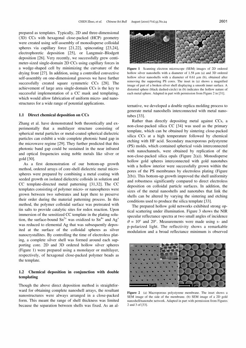
As a first demonstration of our bottom-up growth method, ordered arrays of core-shell dielectric metal micro- spheres were prepared by combining a metal coating with seeded growth on isolated dielectric colloids in solution and CC template-directed metal patterning [31,32]. The CC templates consisting of polymer micro- or nanospheres were grown between two substrates and kept there to preserve their order during the material patterning process. In this method, the polymer colloidal surface was pretreated with tin salts to provide catalytic sites for redox reaction. Upon immersion of the sensitized CC template in the plating solu-tion, the surface-bound Sn2+ was oxidized to Sn4+ and Ag+ was reduced to elemental Ag that was subsequently depos-ited at the surface of the colloidal spheres as silver nanocrystallites. By controlling the time of electroless plat-ing, a complete silver shell was formed around each sup-porting core. 2D and 3D ordered hollow silver spheres (Figure 1) were prepared using a monolayer or multilayer, respectively, of hexagonal close-packed polymer beads as the template.
1.2 Chemical deposition in conjunction with double templating
Though the above direct deposition method is straightfor-ward for obtaining complete nanoshell arrays, the resultant nanostructures were always arranged in a close-packed form. This meant the range of shell thickness was limited because the separation between shells was fixed. As an al-
Figure 1 Scanning electron microscope (SEM) images of 2D ordered hollow silver nanoshells with a diameter of 1.58 μm (a) and 3D ordered hollow silver nanoshells with a diameter of 0.61 μm (b), obtained after removing the supporting PS cores. The inset in (a) shows a magnified image of part of a broken silver shell displaying a smooth inner surface. A distorted sphere (black dashed-circle) in (b) indicates the hollow nature of each metal sphere. Adapted in part with permission from Figure 2 in [31].
ternative, we developed a double replica molding process to generate metal nanoshells interconnected with metal nano-tubes [33].
Rather than directly depositing metal against CCs, a non-close-packed silica CC [34] was used as the primary template, which can be obtained by sintering close-packed silica CCs at a high temperature followed by chemical etching with HF acid. Secondary macroporous polystyrene (PS) molds, which contained spherical voids interconnected with nanochannels, were obtained by replication of the non-close-packed silica opals (Figure 2(a)). Monodisperse hollow gold spheres interconnected with gold nanotubes with a hollow interior were successfully grown within the pores of the PS membranes by electroless plating (Figure 2(b)). This bottom-up growth improved the shell uniformity and robustness significantly compared to direct electroless deposition on colloidal particle surfaces. In addition, the sizes of the metal nanoshells and nanotubes that link the shells can be altered by varying the sintering and etching conditions used to produce the silica template [33].
The prepared hollow gold networks exhibited strong op-tical scattering under illumination. Figure 3 shows the NIR specular reflectance spectra at two small angles of incidence θ = 10° and 20°. Measurements were made using s- and p-polarized light. The reflectivity shows a remarkable modulation and a broad reflectance minimum is observed
Figure 2 (a) Macroporous polystyrene membrane. The inset shows a SEM image of the side of the membrane. (b) SEM image of a 2D gold nanoshell/nanotube network. Adapted in part with permission from Figures 2 and 3 of [33].

2602 CHEN Zhuo, et al. Chinese Sci Bull August (2010) Vol.55 No.24
Figure 3 NIR specular reflectance spectra of a 2D gold nanoshell/nanotube network under s-polarization (a) and p-polarization (b) at two off-normal inci-dence angles: θ = 10° and 20°. The sample is that shown in Figure 2(b). Reprinted with permission from Figure 5 of [33].
for both polarizations. The difference in the location of the minimum between both polarization states is minor at a small angle of incidence (θ = 10°), which is consistent with the hexagonal symmetry of the structure. However, this difference became significant between the two polarizations when the angle of incidence was increased to θ = 20°. It is also noted that a new weak reflectance band evolves at 1650 nm for the p state. The optical responses are related to the collective light scattering and propagation of surface plas-mons in these plasmonic microstructures. Numerical simu-lation that takes scattering and surface plasmons in gold nanoshells and nanotubes into account must be considered to explain the observed strong reflectivity modulations and their different responses to the angle of incidence.
1.3 Direct physical deposition on colloidal crystals
The simplest way to form ordered arrays of metal nanopar-ticles of a particular shape is to physically deposit a thin layer of metal directly onto the surface of a 2D CC template [35]. Using this process, each microbead will be hemi-spherically covered with metal and the resulting metal film consists of an array of metal half-shells. The shell size is dictated by the spheres in the template, which can be easily controlled from 200 nm to several micrometers. Figure 4(a) shows the SEM image of a typical sample made from gold.
In 1998, Ebbesen et al. [36] first reported extraordinary optical transmission (EOT) in an opaque metal film perfo-rated with a 2D array of subwavelength holes. This unusual
phenomenon is now commonly understood to occur as a result of diffractive coupling to evanescent surface plasmon polaritons (SPPs), which leads to a strong concentration of light at the metal surface. This light then tunnels through the holes in the film, reradiating by the inverse process on the exit side. The SPPs on the metal film patterned on the CC surfaces also displayed anomalous transmission but with unusual dispersion compared to that from metal films on a flat substrate [35].
Figure 4(b) shows the transmission spectra of thin gold layers deposited on silica and polystyrene CCs under nor-mal incidence of linearly polarized light. A strong, extraor-dinary transmission peak is observed for each case. This is compared to the negligible transmission observed for the homogeneous gold film deposited directly on a planar quartz substrate (dotted line in Figure 4(b)). The peak wavelength is dependent on the dielectric properties of the CC substrate. More importantly, the transmission features vary dramatically as the thickness of the gold film is in-creased. A transition from the excitation of localized SP resonance to extended SP propagation at a critical metal film thickness is apparent (Figure 5).
Our successful fabrication of centimeter-sized CCs [27] allowed us to further measure the dispersion properties of plasmonic crystals, which are shown in Figure 6. At small angles of incidence, the resonances show similar dispersion behavior even though the in-plane wavevector is aligned along different major axes of the first Brillouin zone. How-ever, the difference in the resonance dispersion becomes
Figure 4 (a) SEM image (tilted view) of a highly corrugated gold film deposited on a 2D CC. The thickness of the gold shells on top of the spheres is about 30 nm. (b) Transmission spectra of a textured gold film on different monolayer silica and polystyrene CCs. The silica and polystyrene spheres have a diameter dsilica = 1.58 μm and dPS = 1.59 μm, respectively. The dotted line shows the transmission spectrum of an unpatterned gold film on a flat quartz chip. Reprinted with permission from Figures 1 and 2 of [35].

CHEN Zhuo, et al. Chinese Sci Bull August (2010) Vol.55 No.24 2603
Figure 5 In situ transmission spectra of a series of gold-deposited 2D silica CCs (dsilica = 1.58 μm). The thickness of the gold shell was increased from 0 (curve A) to 48 nm (curve N). The grey solid lines in the bottom plane are the corresponding projections of the transmission spectra; their intersections with the shell-thickness axis show the thickness of the corre-sponding gold layer. Reprinted with permission from Figure 5 of [35].
noticeable when the incident angle is increased beyond θ = 8°, especially for the transmission spectrum in the short wavelength region. It is noted that a new mode in the long wavelength regime is observed only under p-polarization when θ is increased beyond 8° for both sample orientations (Figure 6(a) and (c)). This mode could be explained to oc-cur as a result of the excitation of a SP mode localized on the hemispherical gold shells [37,38].
1.4 Electrochemical deposition on a doubly templated mold
So far we have demonstrated how to manipulate physical or chemical methods using CCs as templates to prepare 2D arrays of metallic complete shells, non-close-packed nano-
Figure 6 Transmission spectra of a plasmonic crystal fabricated by sput-tering a gold layer with a thickness of 33 nm onto a single domain 2D polystyrene CC substrate. The diameter of the polystyrene colloidal beads is 1.58 μm. Reprinted with permission from Figure 5 of [27].
shells and half-shells. In this section, a doubly templated electrochemical deposition technique that allows for further shaping of the resultant half-shells is demonstrated, thus creating uniform metallic colloids in a 2D rigid format with controlled cavity sizes [39].
In a typical experiment, a metal film shaped like an egg carton was formed on the surface of a silica CC template via metal thermal evaporation that was then attached to a metal wire. A freestanding polymer macroporous membrane was double-templated against the silica CC template. The poly-mer structures, now containing the metal network, acted as a cathode for metal electrochemical deposition under a re-verse voltage with a rectangular wave pulse. The voltage is characterized by the cathode and anode potentials Ucath and Uanod, and the pulse width of each polarity τcath and τanod, respectively (Figure 7(a)). The technique allowed ordered arrays of metallic colloids to be electrochemically fabri-cated within the pores of the polymer molds.
We first demonstrated the fabrication of uniform hollow hemispheres with controlled wall thickness over a wide range. This was achieved through our observation that cop-per deposition was restricted radially on the mother Au half-shell array surface when the cathode potential was rela-tively low [40]. Figure 7(b) shows the SEM image of such a typical sample. In this case, the thickness of the Cu half-shells can be readily controlled by regulating the amount of transferred charge. Figure 7(c) shows the meas-ured thickness of the Cu shells as a function of the deposi-tion charge. The results agree well with the theoretical val-ues for wall thicknesses less than 310 nm when silica tem-plate spheres with a diameter of 1.6 µm were used.
In addition, we confirmed experimentally that further metal growth beyond the sides of the half-shells can be eas-ily initiated in our templating method by applying relatively high cathode voltages to the plating cells. In these cases, rigid arrays of monodisperse metallic colloids with cup- or funnel-shaped cavities can be prepared. Figure 8 shows SEM images of Cu arrays prepared under the conditions Ucath = −0.8 V, τcath = 80 ms, Uanod = 0.4 V, and τanod = 20 ms with different deposition times. Cup-shaped (Figure 8(a)) and funnel-shaped (Figure 8(b)) cavities can be ob-tained, as well as solid spheres when the PS pores were nearly filled (Figure 8(c)). Both the shape and size of the cavities in the metallic nanocups can be manipulated in our method by controlling the pulsed voltage or the total charge passed during Cu deposition.
Our recent theoretical study shows that light can tunnel through a monolayer of hexagonal-close-packed metallic shells with a dielectric core, through excitation of a variety of SPs [38]. Because the fabricated metal microstructures are freestanding in nature, they could allow light tunneling via the excitation of SP modes. This prediction has been partially confirmed experimentally, as demonstrated in Fig-ure 9(a), which shows the transmission spectrum measured

2604 CHEN Zhuo, et al. Chinese Sci Bull August (2010) Vol.55 No.24
Figure 7 (a) Schematic diagram of a two-electrode system for copper deposition under a reverse voltage with a rectangular wave pulse; (b) SEM image of rigid arrays of Cu half-shells; (c) Measured and predicted relationships between the shell thickness and deposition charge. Adapted in part with permission from Figure 1 of [39].
Figure 8 SEM images (tilted view) of rigid arrays of hollow Cu colloids with cup-shaped (a), funnel-shaped cavities (b) and solid Cu spheres (c). Reprinted with permission from Figure 2 of [39].
for the Cu hollow nanocups (Figure 8(a)) under normal in-cidence of light. The results from numerical simulation are plotted in Figure 9(b), which confirmed the main transmis-sion peak as well as the subpeaks observed in experiments. The distributions of the electric field amplitude at the transmission resonances were also calculated and are shown in the insets of Figure 9(b). The resonances predicted at 1050 nm were rationalized to result from a partially local-ized SP mode (cavity mode) because the remarkable field
enhancement is concentrated within the cavities [41]. The main peak at 2070 nm could arise from the excitation of a highly localized SP mode with its electric field tightly con-fined at the nanogaps between adjacent metallic colloidal particles [41]. In addition, the mode at 1250 nm predicted in the calculation for the nanocup array could be explained as contribution from a delocalized SP mode excited in the structure because the corresponding enhanced field is not tightly confined within the nanogaps, but instead extends into the surrounding medium (i.e. air) from the particle sur-face with multiple nodes [41].
2 Quasi-3D plasmonic materials as refractive index sensors
Because the properties of plasmonic crystals are closely re-lated to refractive index (RI) of the dielectric adjacent to the metal film, the transmission resonances in plasmonic crystals can be monitored to detect RI changes in the environment [42–46]. The advantages of the EOT effect based sensors include a simple measurement geometry and great promise for a significant increase in density of the detection array.
Figure 9 (a) Measured normal incidence transmission spectrum for the Cu hollow nanocup array (Figure 8(a)). Inset shows the top view of the nanocups. (b) Numerical simulation of the transmission spectrum. Insets show the calculated electric field amplitude distributions along the xoz-plane at the transmis-sion resonances. Adapted in part with permission from Figure 3 of [39].

CHEN Zhuo, et al. Chinese Sci Bull August (2010) Vol.55 No.24 2605
Motivated by the simplicity of our bottom-up fabrication method and the observed enhanced transmission character-istics (see Figure 4(b)), the quasi-3D metallic nanohole ar-rays were further studied to assess their potential for appli-cation as a SP sensor [47]. The sensitivity of the main transmission resonance of the metallic hollow half-shell array sensors can reach a value of 1192 nm/RIU change of the surrounding medium, which is a fivefold increase com-pared to that found before removal of the CC [48]. The sen-sitivity of the hollow Au half-shell array also outperforms previous individual or random ensembles of metallic nanoparticles including nanoprisms [49], half-coated col-loids [50], shells [51], nanorices [52], rings [53] and cres-cents [54], which instead rely on localized SP enhanced absorption and scattering.
Figure 10(a) and (b) shows the transmission spectra measured for the quasi-3D Au nanohole arrays, with and without a silica CC template, in three different host materi-als. The plasmonic crystals composed of a monolayer of interconnected hollow metal half-shells display the same transmission resonances in air as the as-prepared metallodi-electric structures containing the CC template [35,55]. For the hollow shell array, the main peak (located at 1251 nm in air) shifts substantially to longer wavelength as the RI of the surrounding environment increases. This change is accom-
panied with band broadening but without much variation in resonance amplitude. Unfortunately, this shift is quite small for the structure containing the CC template. The amplitude of the main peak also showed a substantial decrease as the matrix RI increased before removal of the CC. Figure 10(c) summarizes the change in wavelength of the main peak as a function of RI for both plasmonic crystals. The gradients give a sensitivity (defined as S = Δλ/Δn) of 1192 nm/RIU for the interlinked hollow half-shell array and 223 nm/RIU for the as-prepared structure.
The underlying physics that give rise to an enhanced sensitivity for the quasi-3D plasmonic crystal after removal of the CC can be understood as follows. For the plasmonic structure containing the CC, a large portion of the field is localized inside the dielectric spheres at the main resonance, as confirmed by our numerical simulations [47]. This ex-plains why a small change in transmission resonance wave-length was observed when the CC-supported plasmonic structure was immersed into solvents with different RI [48]. When the CC template is removed so that the half-shell ar-ray is supported directly on a planar substrate, the RI dif-ference across the metal films reduces to a minimum, thus enabling resonant coupling of SPs on the opposite surfaces of the hole array [56]. In this case, the maximum electric fields observed are exclusively distributed within the shells
Figure 10 Measured transmission spectra for the as-prepared plasmonic structure (a) and the quasi-3D metallic nanohole array after removal of the CC template (b) immersed in different host materials: air (solid line, n = 1.0), CCl4 (dashed line, n = 1.46) and CS2 (dotted line, n = 1.63). The insets show the magnified SEM images of the measured plasmonic structures. The template silica spheres had an initial diameter of 1.58 µm and the Au film has a nominal thickness of ~50 nm. (c) Plot of the shift of the main peak vs. RI for the as-prepared plasmonic structure (triangles) and the quasi-3D Au nanohole array (squares). Adapted in part with permission from Figure 3 of [47].
above the substrate. The sensitivity of our quasi-3D plas-monic crystals can be enhanced because this index-matching condition is guaranteed in liquids (or gases) with arbitrary RI, due to the hollow nature of the 3D plasmonic structure.
3 Conclusions
In summary, we have developed a variety of bottom-up growth templating approaches for the fabrication of novel plasmonic nanomaterials. Using physical, chemical or elec-
trochemical deposition of metal with the aid of 2D CC tem-plates, rigid arrays of metallic colloids with a constant morphology were obtained in exclusively a freestanding format. In addition, we investigated the optical properties of the metallic nanoparticle arrays and their dependence on geometry. The SP modes supported by these plasmonic structures were analyzed and confirmed numerically. This low-cost and efficient fabrication technique developed here substantially increases the attractiveness of using these plasmonic structures as nanophotonic elements in applica-tions, including SP enhanced optical sensing and spectros-

2606 CHEN Zhuo, et al. Chinese Sci Bull August (2010) Vol.55 No.24
copy [42–46,57–60]. We believe that these novel plasmonic crystals may find application in biosensing, imaging, sur-face enhanced Raman scattering and optoelectronics.
This work was supported by the State Key Program for Basic Research of China, NSFC and NCET (10734010, 50771054, 10804044, NCET-09- 0453). This work was also partially sponsored by NSFC under Excellent Youth Foundation and RFDP.
1 Kreibig U, Vollmer M. Optical Properties of Metal Clusters. Berlin: Springer, 1995
2 Yao H M, Li Z, Gong Q H. Coupling-induced excitation of a forbid-den surface plasmon mode of a gold nanorod. Sci China Ser G-Phys Mech Astron, 2009, 52: 1129–1138
3 Li Z, Gong Q H. The plasmonic coupling of metal nanoparticles and its implication for scanning near-field optical microscope characteri-zation. Chinese Sci Bull, 2009, 54: 3843–3843
4 Haynes C, Van Duyne R P. Nanosphere lithography: A versatile nanofabrication tool for studies of size-dependent nanoparticle optics. J Phys Chem B, 2001, 105: 5599–5611
5 Auguié B, Barnes W L. Collective resonances in gold nanoparticle arrays. Phys Rev Lett, 2008, 101: 143902
6 Maier S A, Brongersma M L, Kik P G, et al. Plasmonics-A route to nanoscale optical devices. Adv Mater, 2001, 13: 1501–1505
7 Barnes W L, Dereux A, Ebbesen T W. Surface plasmon subwave-length optics. Nature, 2003, 424: 824–830
8 Atwater H. The promise of plasmonics. Sci Am, 2007, 296: 56–63 9 Anker J N, Hall W P, Lyandres O, et al. Biosensing with plasmonic
nanosensors. Nat Mater, 2008, 7: 442–453 10 Liu J B, Dong W, Zhan P, et al. Synthesis of bimetallic nanoshells by
an improved electroless plating method. Langmuir, 2005, 21: 1683– 1686
11 Liu J B, Li N, Wang S Z, et al. A facile synthesis of silver-coated composite particles by swelling surface method. Chin Phys Lett, 2005, 22: 975–977
12 Chen Z, Wang Z L, Zhan P, et al. Preparation of metallodielectric composite particles with multi-shell structure. Langmuir, 2004, 20: 3042–3046
13 Chen Z, Zhan P, Zhang J H, et al. Preparation of silver-coated poly-styrene composite particles. Chin Phys Lett, 2003, 20: 1369–1371
14 Ahmadi T S, Wang Z L, Green T C, et al. Shape-controlled synthesis of colloidal platinum nanoparticles. Science, 1996, 272: 1924–1926
15 Sun Y, Xia Y. Shape-controlled synthesis of gold and silver nanopar-ticles. Science, 2002, 298: 2176–2179
16 Tao A, Sinsermsuksakul P, Yang P. Polyhedral silver nanocrystals with distinct scattering signatures. Angew Chem Int Ed, 2006, 45: 4597–4601
17 Glotzer S C, Solomon M J. Anisotropy of building blocks and their assembly into complex structures. Nat Mater, 2007, 6: 557–562
18 Kalsin A M, Fialkowski M, Paszewski M, et al. Electrostatic self-assembly of binary nanoparticle crystals with a diamond-like lat-tice. Science, 2006, 312: 420–424
19 Narayanan S, Wang J, Lin X M. Dynamical self-assembly of nanocrystal superlattices during colloidal droplet evaporation by in situ small angle X-ray scattering. Phys Rev Lett, 2004, 93: 135503
20 Tao A R, Ceperley D P, Sinsermsuksakul P, et al. Self-organized sil-ver nanoparticles for three-dimensional plasmonic crystals. Nano Lett, 2008, 8: 4033–4038
21 Kim E, Xia Y, Whitesides G M. Micromolding in capillaries: Appli-cations in materials science. J Am Chem Soc, 1996, 118: 5722–5731
22 Jiang P, Bertone J F, Hwang K S, et al. Single-crystal colloidal mul-tilayers of controlled thickness. Chem Mater, 1999, 11: 2132–2140
23 Jiang P, Prasad T, McFarland M J, et al. Two-dimensional non-close-packed colloidal crystals formed by spincoating. Appl Phys Lett, 2006, 89: 011908
24 Mihi A, Ocaña M, Míguez H. Oriented colloidal-crystal thin films by spin-coating microspheres dispersed in volatile media. Adv Mater, 2006, 18: 2244–2249
25 Zhang K Q, Liu X Y. In situ observation of colloidal monolayer nu-cleation driven by an alternating electric field. Nature, 2004, 429: 739–742
26 van Duffel B, Ras R H A, De Schryver F C, et al. Langmuir-Blodgett deposition and optical diffraction of two-dimensional opal. J Mater Chem, 2001, 11: 3333–3336
27 Sun J, Tang C J, Zhan P, et al. Fabrication of centimeter-sized sin-gle-domain two-dimensional colloidal crystals in a wedge-shaped cell under capillary forces. Langmuir, 2010, 26: 7859–7864
28 Sun J, Li Y Y, Dong H, et al. Fabrication and light transmission properties of monolayer square symmetric colloidal crystals via con-trolled convective self-assembly on 1D grooves. Adv Mater, 2008, 20: 123–128
29 Zhang W Y, Lei X Y, Wang Z L, et al. Robust photonic band gap from tunable scatterers. Phys Rev Lett, 2000, 84: 2853–2856
30 Wang Z L, Chan C T, Zhang W Y, et al. Three-dimensional self-assembly of metal nanoparticles: Possible photonic crystal with a complete gap below the plasma frequency. Phys Rev B, 2001, 64: 113108
31 Chen Z, Zhan P, Wang Z L, et al. Two- and three-dimensional ordered structures of hollow silver spheres prepared by colloidal crystal templating. Adv Mater, 2004, 16: 417–422
32 Zhan P, Liu J B, Dong W, et al. Reflectivity behavior of two-dimensional ordered array of metallodielectric composite parti-cles at large incidence angles. Appl Phys Lett, 2005, 86: 051108
33 Dong W, Dong H, Wang Z L, et al. Ordered array of gold nanoshells interconnected with gold nanotubes fabricated by double templating. Adv Mater, 2006, 18: 755–759
34 Fenollosa R, Meseguer F. Non-close-packed artificial opals. Adv Mater, 2003, 15: 1282–1285
35 Zhan P, Wang Z L, Dong H, et al. The anomalous infrared transmis-sion of gold films on two-dimensional colloidal crystals. Adv Mater, 2006, 18: 1612–1616
36 Ebbesen T W, Lezec H J, Ghaemi H F, et al. Extraordinary optical transmission through sub-wavelength hole arrays. Nature, 1998, 391: 667–669
37 Maaroof A I, Cortie M B, Harris N, et al. Mie and Bragg plasmons in subwavelength silver semi-shells. Small, 2008, 4: 2292–2299
38 Ye J, Verellen N, Van Roy W, et al. Plasmonic modes of metallic semishells in a polymer film. ACS Nano, 2010, 4: 1457–1464
39 Chen Z, Dong H, Zhan P, et al. Monolayer rigid arrays of cav-ity-controllable metallic mesoparticles: Electrochemical preparation and light transmission responances. Appl Phys Lett, 2010, 96: 051904
40 Yoo W C, Lee J K. Field-dependent growth patterns of metals elec-troplated in nanoporous alumina membranes. Adv Mater, 2004, 16: 1097–1101
41 Tang C J, Wang Z L, Zhang W Y, et al. Localized and delocalized surface-plasmon-mediated light tunneling through monolayer hex-agonal-close-packed metallic nanoshells. Phys Rev B, 2009, 80: 165401
42 Brolo A G, Gordon R, Kavanagh K L. Surface plasmon sensor based on the enhanced light transmission through arrays of nanoholes in gold films. Langmuir, 2004, 20: 4813–4815
43 Liu Y, Williams L, Blair S, et al. Biosensing based upon molecular confinement in metallic nanocavity arrays. Nanotechnology, 2004, 15: 1368–1374
44 Tetz K A, Pang L, Fainman Y. High-resolution surface plasmon resonance sensor based on linewidth-optimized nanohole array transmittance. Opt Lett, 2006, 31: 1528–1530
45 De Leebeeck A, Kumar L K, De Lange V, et al. On-chip sur-face-based detection with nanohole arrays. Anal Chem, 2007, 79: 4094–4100
46 Pang L, Hwang G M, Slutsky B, et al. Spectral sensitivity of two-dimensional nanohole array surface plasmon polariton resonance sensor. Appl Phys Lett, 2007, 91: 123112

CHEN Zhuo, et al. Chinese Sci Bull August (2010) Vol.55 No.24 2607
47 Li Y Y, Pan J, Zhan P, et al. Surface plasmon coupling enhanced di-electric environment sensitivity in a quasi-three-dimensional metallic nanohole array. Opt Express, 2010, 18: 3546–3555
48 Li Y Y, Sun J, Wang L, et al. Surface plasmon sensor with gold film deposited on two-dimensional colloidal crystals. Appl Phys A, 2008, 92: 291–294
49 Jensen T R, Schatz G C, Van Duyne R P. Nanosphere lithography: Surface plasmon resonance spectrum of a periodic array of silver nanoparticles by ultraviolet-visible extinction spectroscopy and elec-trodynamic modeling. J Phys Chem B, 1999, 103: 2394–2401
50 Himmelhaus M, Takei H. Cap shaped gold nanoparticles for an opti-cal biosensor. Sens Actuators B Chem, 2000, 63: 24–30
51 Tam F, Moran C, Halas N J. Geometrical parameters controlling sen-sitivity of nanoshell plasmon resonances to changes in dielectric en-vironment. J Phys Chem B, 2004, 108: 17290–17294
52 Wang H, Brandl D W, Le F, et al. Nanorice: A hybrid plasmonic nanostructure. Nano Lett, 2006, 6: 827–832
53 Larsson E M, Alegret J, Käll M, et al. Sensing characteristics of NIR localized surface plasmon resonances in gold nanorings for applica-
tion as ultrasensitive biosensors. Nano Lett, 2007, 7: 1256–1263 54 Bukasov R, Shumaker-Parry J S. Highly tunable infrared extinction
properties of gold nanocrescents. Nano Lett, 2007, 7: 1113–1118 55 Landström L, Brodoceanu D, Piglmayer K, et al. Infrared transmis-
sion through metalcoated lattices of microspheres. Appl Phys A, 2005, 81: 15–16
56 Krishnan A, Thio T, Kim T J, et al. Evanescently couples resonance in surface plasmon enhanced transmission. Opt Commun, 2001, 200: 1–7
57 Reilly T H, Chang S H, Corbman J D, et al. Quantitative evaluation of plasmon enhanced Raman scattering from nanoaperture arrays. J Phys Chem C, 2007, 111: 1689–1694
58 Brolo A, Arctander E, Gordon R, et al. Nanohole-enhanced Raman scattering. Nano Lett, 2004, 4: 2015–2018
59 Liu Y, Blair S. Fluorescence enhancement from an array of sub-wavelength metal apertures. Opt Lett, 2003, 28: 507–509
60 Brolo A G, Kwok S C, Moffitt M G, et al. Enhanced fluorescence from arrays of nanoholes in a gold film. J Am Chem Soc, 2005, 127: 14936–14941


![Enhancing the Angular Sensitivity of Plasmonic Sensors ...biotheory.phys.cwru.edu/PDF/AOM.pdf · ultrasensitive plasmonic biosensors.[29,30] A plasmonic nanorod metamaterial (Type](https://static.fdocuments.in/doc/165x107/5fcdd2c6db367d06a677e7be/enhancing-the-angular-sensitivity-of-plasmonic-sensors-ultrasensitive-plasmonic.jpg)

