
Book of Abstracts - IRAMISiramis.cea.fr/.../20081006AbstractBook.pdfsurfactant encapsulated crystals...
35
Book of Abstracts
Transcript of Book of Abstracts - IRAMISiramis.cea.fr/.../20081006AbstractBook.pdfsurfactant encapsulated crystals...

Book of Abstracts


Workshop Programme
Monday Oct 6
Inaugural Session (0900 – 1030hrs.) Welcoming Introduction by CEA/DSM Introduction to the Workshop by Dr. P. Boulanger/ DR. J. Yakhmi Introductory Talk by JP Bourgoin: "Nanoscience Programme at CEA"
Session I (1100 – 1230) Chairman : Dr. J.P Bourgoin 1. Dr. J.V. Yakhmi: "Device fabrication using self-assembly routes" 2. Dr. F. Cléri: "Self-assembly of molecules on Si: theoretical approaches"
Session II (1400 – 1730 hrs.) Chairman Dr. G. Bidan 1. Dr. R. Mallik: "Focussed Lasers, Mutant Flies and Hungry Cells: Understanding Nanoscale Machines designed by Nature". 2. Dr. K. Das: “Studies on Silica and metallic nanoparticles and their possible use for bio-medical applications” 3. Dr. Y. Roupioz: "Protein microarrays for living cell analysis" 4. Dr. P. Mailley: "Micro and nanoelectrochemistry: a versatile tool for the design of biosensors and biochips" 5. Dr. A. Filoramo: "Bio-directed assembly of carbon nanotubes for molecular electronics"
Tuesday Oct 7
Session III (0900 – 1230 hrs.) Chairman Prof. B. Bhushan 1. Dr. V. Saxena: “Poly(3-hexylthiophene) based Field Effect Transistors using SiO2 gate dielectric modified with 3-aminopropyltrimethoxysilane (APTMS) multilayers” 2. Dr. T. Melin: " Electrostatic properties of CNT and CNT based devices using Scanning Force Techniques" 3. Dr. F. Duclairoir: "Redox monolayers & bistable molecules for memory applications" 4. Dr. G. Robert: "Carbon nanotubes / Self-assembled monolayers hybrid devices"
Session IV (1400 – 1730 hrs.) Chairman Dr. D. Vuillaume 1. Prof. B. Bhushan (invited guest OHIO Univ.): “Nanotribology, Nanomechanics and Materials Characterization Studies: Applications to Bio/Nanotechnology & Biomimetics” 2. Dr. J. Philip: "Thermal properties of magnetic nanofluids". 3. Dr. D. Carrière: “Synthesis of nanoparticles at interfaces”. 4. Dr. S. Palacin: "Grafting organics on surfaces: methods and applications" 5. Dr. N. Clément: ""Measurement (1/f noise, RTS) in molecular junction"
Wednesday Oct 8
Session V (0900 – 1230 hrs.) Chairman Dr. P. Boulanger 1. Dr. M. Sanyal: "Low dimensional physics using soft nanomaterials" 2. Dr. J. Daillant: "Nanoparticles at the water-oil interface: emulsion stabilization and organisation" 3. Dr. S. Neogy : "Interfaces in nanocrystalline zirconium based alloys" 4. Dr. D.Khushalani: "Synthesis of functional oxide materials: manipulating morphology". 5. Dr. R. Demadrille: "Nanostructured Polymers and Composites for Applications in Organic Photovoltaic Devices"
Thursday Oct 9
Session VI (0900 – 1230 hrs.) Chairman Dr. M. Sanyal 1. Dr. S. Bhunia: "MOCVD & CVD growth of compound semiconductor nanostructures" 2. Dr. M. Mayne/M. Pinault: "Nucleation and growth mechanism of Carbon nanotubes, application in materials science" 3. Dr. Y. Coffinier: "Si nanowire: growth, functionalization and applications" 4. Dr. B. Jousselme: "Synthesis and grafting of n and p type σ-π-σ systems on substrates for molecular electronic applications". 5. Dr. G. Dambrine: "High-frequency behavior of CNT transistors"
Friday Oct 10
Session VII (0900 – 1230 hrs.) Chairman Dr. J.V. Yakhmi 1. Dr. S.N. Sahu: "Quantum dots and self-assembled Q.dot-DNA hybrids for device interface and biosensor applications" 2. Dr. N. Herlin-Boime: "Si Nanocrystals: synthesis & functionalisation for life science applications" 3. Dr. G. Carrot: "Nanoscale hybrid object: from 3D small angle neutron scattering study to tunable 2D arrays formation" 4. Dr. H. Perez: "Bottom up approach for the elaboration of nanocomposite model structures" based organically capped Pt Nanoparticles electrocatalyst”
Closing session : Dr. J.V. Yakhmi and Dr. P. Boulanger


Session I - 1 Device Fabrication using Self-assembly Routes
J.V. Yakhmi
Bhabha Atomic Research Centre, Mumbai – 400 0085, India
Self-assembly is uniquely advantageous for the development of molecular/organic electronic devices or sensors, which require precise control molecular arrangement in an active element. In the present talk, we highlight our recent attempts, at BARC, to prepare functional molecular materials, and their films (SAMs or LB), to fabricate devices based on them.
We shall describe the use of DNA, or a SAM, a surfactant monolayer at the air-water-
interface, or simply the liquid-liquid interface as templates for growth of functional materials, including single crystals of PANI. Towards the fabrication of sensors, we shall give typical examples of our attempts to prepare gas sensors from LB films of polymers, or K-ion sensors from LB films of surfactant encapsulated crystals of Prussian Blue Analogues.
In the field of molecular electronics, long alkyl chains consisting of � bonds can act as
dielectric, ��� molecules as rectifier and/or transistor, and ����� molecules as resonant tunnel diodes. Covalent electro-grafting of organic monolayers such as OTS or TPP-11, a porphyrin derivative, has been carried out in our lab for improved Si-hybrid electronics. We shall also touch upon our attempts to deposit SAMs of alkyl-chains having C atoms varying between 3-18 atoms, APTMS and FePc, on Si-substrates for device fabrication.

Session 1 - 2 Self-assembly of molecules on Si: theoretical approaches
Fabrizio CLERI
Institut d’Electronique, Microélectronique et Nanotechnologie (UMR Cnrs 8520)
Université des Sciences et Technologies de Lille Av. Poincaré, BP 60069, F-59652 Villeneuve d’Ascq (France)
[email protected] http://physique.iemn.univ-lille1.fr/
The rapid development of nanotechnology calls for precise information on the atomic-scale structure of modern devices constructed via molecule deposition on surfaces. Theory has to make this information accessible at extended space and temporal scale, with no loss of reliability. By proposing a multi-scale approach based on a combined use of density functional molecular dynamics, first-principles inspired interatomic potentials and statistical MonteCarlo methods we aim at fulfilling this goal. Selected systems (supramolecular structures on semiconductor surfaces, organic molecules for surface coating and hybrid nanostructures) are taken from those of current experimental interest at IEMN.
A realistic interpretation of the adsorption phenomena of molecules at a surface requires precise knowledge of three main factors: a) the physical and chemical interaction processes between the adsorbed species and the substrate, b) the structure and electronic states of the surface itself and c) the physical conditions under which the adsorption takes place. The recent focus of atomic-scale modeling has been typically on the chemical interaction between an isolated molecule and a perfect, defect free model surface. The methods employed include first principles electronic-structure calculations using the density-functional theory (DFT) and different levels of semiempirical approximations. To address such issues as morphology and thermal growth, with no loss of information and accuracy on chemical bonding, the above studies need to be recast within a multi-scale simulation strategy. The goal is to achieve a realistic description of the newly created molecules-surface systems at all length and time scales relevant to experimental observations.
Molecular dynamics (MD) simulations can give access to a large wealth of information on the local conditions of contact between molecule and surface, the adhesion and diffusion barriers at finite temperature, the vibrational spectra and collective modes of the aggregates, the reaction-dissociation equilibrium between the different adsorbed species, and so on. The inter-atomic forces necessary to perform MD simulations should be ideally provided by full-fledged, electronic-structure based first-principles calculations. However, due to the challenging computational effort of these applications, more approximate interaction schemes will continue to play a major role, provided their predictive power is accurately assessed. These can be either empirical force fields adjusted on experimental molecular data, or generic functional forms more specialized in the description of the condensed phases of materials. As far as the time scale is concerned, either coarse-grained MD with effective potentials, or the kinetic Monte Carlo (KMC) method can directly simulate the deposition and growth process over time scales inaccessible to standard MD. Input information to KMC models can be obtained from fitting of specific configurations to first-principles electronic structure reference calculations.

Session II - 1 Focussed Lasers, Mutant Flies and Hungry Cell
Understanding Nanoscale Machines designed by Nature
Virupakshi Soppina, Arpan Rai, Avin Ramaiya, Pradeep Barak, Roop Mallik
Department of Biological Sciences, Tata Institute of Fundamental Research, Mumbai, India ABSTRACT Molecular motors are remarkable and robust nanoscale machines designed by nature to transport cellular material as cargo within the cell. This transport is an active driven process, wherein a single motor generates forces of the order of pico Newtons to effect transport of micron sized cargoes within the highly viscoelastic cellular medium. The technique of optical tweezers is very well suited to measure the forces and nanometer steps taken by single motors, and such biophysical studies have been at the forefront of single molecule interdisciplinary research. Unfortunately, such “single molecule” experiments are always done under artificial conditions, and therefore do not reveal much about how motors function within cells. I will stress on the need to extend optical trapping techniques to motor driven transport under more complex and realistic conditions, and the difficulties in doing so. In this situation, the motors never function as single entities – instead, several motors with inclination to walk in different directions may be simultaneously present on a single cargo. Remarkably, the motors appear not to work against each other – instead, their relative activity is regulated precisely so that a desired intracellular distribution of the cargo can be attained. I will introduce an experimental system where we hope to adapt the techniques of single molecule measurements to look inside cells, and attempt to understand this regulation of Molecular motors. The goal is to experimentally probe how collective behaviour arises within a complex of interacting motor proteins. I will also introduce the high temporal (KHz) and spatial resolution (sub-nanometre) biophysical techniques and instrumentation that we are currently developing to address these questions.

Session II - 2 Studies on silica and metallic nanoparticles and their possible use for bio-medical applications
K. Das and P. K. Gupta
Laser Bio-Medical Applications & Instrumentation Division,
Raja Ramanna Center for Advanced Technology, Indore, M.P. 452013 India
[email protected] Several activities related to the use of lasers for biomedical applications like cancer diagnosis, optical imaging, optical micromanipulation and photodynamic therapy are being actively pursued at LBAID, RRCAT. Since nanoscience and nanotechnology are expected to play an important role in this area we have recently initiated an activity on the preparation of nanoparticles and exploration of their use for biomedical imaging, diagnosis and therapy. In this talk, I shall present a brief overview of the work being carried out at LBAID with a particular emphasis on the studies on silica and metallic nanoparticles and their possible use for bio-medical applications Silica based nanoparticles are currently being explored for imaging and drug delivery. Since this requires an understanding of the nature of the interaction between the dye/drug and the nanoparticle, we have studied the photophysical properties of different organic dyes and drugs in presence of organically modified silica nanoparticles. In particular, we have studied the binding of negatively charged photosensitizers, Merocyanine 540 and Chlorin-p6 with silica nanoparticles. Spectroscopic investigations suggest that the photoisomerization rate of Merocyanine 540 bound to silica nanoparticle is significantly reduced. Consistent with the expectation that a reduction in the photoisomerization rate should enhance the singlet oxygen yield of the dye via intersystem crossing, the light induced toxicity of the dye-nanoparticle complex (tested with MCF cells) was observed to be higher compared to the free dye. The interaction between Chlorin-p6 and silica nanoparticles show that the ionization equilibrium for drug that was shown to be a major reason responsible for the selective uptake of the drug in tumor is very different from that for free drug. It was observed that for acidic pH where the free drug exists as hydrophobic aggregates, the presence of SiNP results in the disruption of the aggregates by forming a stable drug-nanoparticle complex. The drug-nanoparticle binding is expected to affect the uptake and photodynamic efficacy of the drug. The size-dependent optical properties of metallic nanoparticles are currently being explored for biomedical diagnosis and therapy. We have studied the nonlinear optical properties of different silver nanostructures like spheres, aggregates of spheres and prisms. Possible use of these for biomedical imaging and sensing will be discussed.

Session II - 3 Protein microarrays for living cell analysis
Roupioz, Y., Mailley, P., Calemczuk, R. and Livache, T.
CREAB, SPrAM UMR CNRS-CEA-UJF 5819,
INAC/CEA-Grenoble, 38054 Grenoble, FRANCE Summary: Among all biological samples, blood is a major source of information for diagnostic purposes. It can be seen as a complex medium containing both dissolved biomolecules and micrometric particles (blood cells) suspended in a carrying liquid (plasma). In the course of designing new miniaturized tools to get access to biological information, we are working on surface functionalization dedicated to blood cell analysis. In the aim of both increasing the throughput and also decreasing the array size, many research groups have attempted to miniaturized the feature size on micro-arrays. We have shown in previous works that pyrrole coupling to biomolecules followed by electro-polymerisation of pyrrole into polypyrrole was an efficient way to functionalize gold covered electrodes. To increase the probe density on a biochip, we proposes new generations of micro-electrochemical reactors dedicated to biochips arraying. This was done using different techniques, such as microelectronics techniques (cf Dr Mailley’s talk). The arrayed biochips were analyzed either using fluorescence microscopy or Surface Plasmon Resonance imaging (SPRi). The strategy for non-adherent cell capture, the surface chemistry chosen for arraying on gold surfaces as well as some of our results on detection of living cells capture on biochips will be presented here.

Session II - 4 Micro and nanoelectrochemistry : a versatile tool for the design of biosensors and biochips
P. Mailley
CEA Grenoble / INAC / SPrAM /CREAB,
17 rue des Martyrs 38054 Grenoble cedex , France, [email protected]
These last years have seen an tremendous research effort on the design of biochips for genomic, proteomic or pharmaceutical applications. The first step in the fabrication of a biochip concerns the “writing” of different biological information onto solid interfaces. Surface modification techniques are thus mainly based on the transfer of pre-synthesised or extracted biological probes on homogeneous or functional surfaces. In such a context, the development of efficient immobilization techniques enabling the spatial control of the deposition process is a key step of biochip design. Moreover, the miniaturization of modified areas is the focus of numbers of research to allow the densification of biological information thus enabling enhanced sensitivity of the capturing and reading behaviours, complexification of the biological information (pharmaceutical screening and decreasing of the required quantities of probes to be immobilized. Furthermore, this size reduction is consistent with the utilization of DNA as templates for the design molecular electronic systems. In such a context, electrochemistry appears as a good candidate for surface modification owing to its addressing capabilities and to the versatility of the immobilization process (electrosorption, electrodeposition, electropolymerisation or electrografting)
Since few years, we developed at CREAB an immobilization strategy based on the electro-co-polymerization of pyrrole and pyrrole bearing biological entities (DNA, polysaccharides, peptides, proteins, biotine). This methodology enables the selective modification of microelectrode within an array with dedicated biological probes. Further developments of this methodology rely with the modification of bulk non-functional surfaces and on the densification of the written biological information in the view of pharmaceutical screening and molecular electronic. This involves the spatial localization of the elctrogenerated spots through either mechanical confinement of the electrolyte (mobile microcell) or electrical confinement of the applied electrodeposition field (scanning electrochemical microscopy, SECM, utilised in the direct mode). In parallel, we also involved such approaches on the electrochemical modification of boron doped diamond interfaces insensitive to electropolymerization through electrografting and on the electrochemically induced decoration of micropores created in insulative materials. Along this talk, an extensive review of these aforementioned works will be presented.

Session II - 5 Bio-directed assembly of carbon nanotubes for molecular electronics
Arianna FILORAMO
with Khoa Nguyen, Chia-Ling Chung, Sebastien Lyonnais, Miguel Monteverde, Stephane Streiff, Stephane Campidelli, Laurence Goux-Capes, Marcelo Goffman, Gael Robert, Vincent
Derycke, Diana Dulic, Christelle Bouchain-Gautier and Jean-Philippe Bourgoin Laboratoire d’Electronique Moléculaire, CEA Saclay, DSM/IRAMIS/SPEC, 91191 Gif-sur-Yvette, France
Thanks to their exceptional electrical, mechanical and chemical characteristics, carbon
nanotubes are very promising building blocks for future nanoelectronic technologies. However, the future of this class of SWNT-based devices is to a large extent related to the development of a bottom-up self-assembly technique. Indeed, at this scale self-assembly, and more generally, “bottom-up” approaches appear to be a more reasonable way to assemble nano-objects into circuits with a two-dimensional and/or three-dimensional layout.
Here, we will briefly present an overview of the current state of the fabrication of devices
made of carbon nanotubes by using self-assembly. In particular, we will discuss a chemical self-assembly route and its use for the realisation of nanotube-based electronic devices. Then, we will focus on DNA-directed approaches: construction of the DNA scaffold, DNA-nanotube chemistry and DNA metallisation. This bio-directed method constitutes a genuine and complete molecular-scale bottom-up method, since it relies on recognition properties inherent to biological entities and can be employed without using any standard nanolithography technique. Indeed, the exceptional recognition properties of DNA molecule make it an ideal candidate for realizing a site-controlled implementation of nanocomponents and its engineering is currently investigated to both create scaffolds and self-assemble nanomaterials.
In conclusion, despite the fact that the degree of maturity of the different nanofabrication
methods is variable, we will make a critical comparison of their perspectives and an analysis of the issues to be solved before they could be integrated to the real-world applications.

Session III - 1 Poly(3-hexylthiophene) based field effect transistors with SiO2 gate dielectric modified
by 3-aminopropyltrichlorosilane multi-layers
Vibha Saxena, A.K. Chauhan, S.P. Koiry, D.K.Aswal, S.K. Gupta, and J.V. Yakhmi
Technical Physics and Prototype Engineering Division, Bhabha Atomic Research Centre, Mumbai-400 085, INDIA.
e-mail: [email protected]
Organic field effect transistors (OFET) are potential candidates for low cost electronics and are therefore investigated for various kinds of applications such as integrated circuits and active-matrix flat-panel displays. In order to improve device characteristics, several methods have been reported employing top-gate OFET, different dielectric materials and buffer layers. Recently, we have demonstrated a process by which –NH2 terminated multilayers of 3-aminopropyltrimethoxysilane (APTMS) can be grafted on SiO2/Si substrates by a self-assembly process [1]. In this talk, the effect of APTMS layers on characteristics of OFET based on poly (3-hexylthiophene) (P3HT) will be discussed. The P3HT films have been prepared on unmodified and APTMS modified SiO2/Si substrates by spin casting method and characterized under ambient conditions. AFM images show that typical P3HT film on the APTMS-modified substrate is significantly smoother than the film deposited on the unmodified substrates. Further, films on APTMS-modified surface show good intergranular connectivity and uniformity and are therefore expected to provide better charge transport and mobility. The effect of substrate preparation on the structure of P3HT films was investigated by UV-Vis and FTIR spectroscopy. The FTIR results show an improved crystallinity and conjugation length of films prepared on the APTMS modified surface. This is supported by optical spectrum of P3HT films on APTMS modified substrates which indicate increase in conjugation length and crystalline order. To study the effect of APTMS interface on OFET, we fabricated and characterized devices with and without APTMS on highly doped p-type silicon substrates (resistivity ~ 1 m� cm). A thermally grown SiO2 layer of 200 nm thickness was used as gate dielectric. It has been demonstrated that the treatment of dielectric with APTMS enhances the field effect mobility (3.2×10⁻² cm2/Vs) as well as the on/off ratio of the devices by two orders of magnitude. This is attributed to conformational changes as well as to an improved uniformity of the spin coat P3HT films on the APTMS-modified substrate as revealed by atomic force microscopy (AFM) and Fourier transform infra red spectroscopy (FTIR) and UV-Vis measurements. REFERENCES
1. A. K. Chauhan, D. K. Aswal*, S. P. Koiry, N. Padma, V. Saxena, S. K. Gupta, and J. V. Yakhmi, Physica Status Solidi, 90 (2008) 581.
2. Vibha Saxena, A.K. Chauhan, N. Padma, D.K.Aswal, S.P. Koiry, Shashwati Sen, R.B. Tokas, S.K. Gupta, C. Sürgers and J.V. Yakhmi, Thin Solid Films (Communicated).
3. D.J. Gundlach, Nature mater., 6 (2007) 4.

Session III - 2 Electrostatic properties of carbon nanotubes and carbon nanotube devices
using scanning force techniques
D. Brunel, M. Zdrojek, H. Diesinger, D. Deresmes and T. Mélin
Institut d’Electronique de Microélectronique et de Nanotechnologie IEMN – CNRS UMR 8520, BP 60069, 59652 Villeneuve d’Ascq Cedex, FRANCE
I will describe in the first part of the talk the electrostatic properties of single-separated multiwalled and single-walled nanotubes (MWCNTs and SWCNTs) probed by charge injection and electric force microscopy (EFM) techniques. Delocalized charge patterns have been observed along nanotubes upon local injection from the EFM tip, corresponding to (i) charge storage in the nanotubes and to (ii) charge trapping in the oxide layer along the nanotubes. The two effects can be separated [1] for CNTs showing abrupt discharge processes in which the charge stored in the CNT is field emitted back to the EFM tip, while trapped oxide charge can subsequently be imaged by EFM, clearly revealing field-enhancement patterns at the CNT caps [2]. The electrostatic properties of individual MWCNT and SWCNTs have then been analyzed from their linear charge densities measured as a function of the nanotube diameters. Results differ from classical capacitive predictions by one order of magnitude, and are understood as a response to the external field generated at the EFM tip. The associated inner-shell charging in the case of MWCNTs is due to their finite transverse polarisability and the intercalation of semiconducting and metallic shells[3].
Iin a second part, I will address the electrostatic properties of CNT field effect transistors probed
by coupled Kelvin Force Microscopy (KFM) and transport measurements, when subjected to a local charge injected in the vicinity of the CNT. The delocalized response of the CNT-FET upon local gating will be discussed[4]. References : [1] M. Zdrojek et al., Phys. Rev. Lett. 96, 39703 (2006); [2] M. Zdrojek et al., Appl. Phys. Lett. 86, 213114 (2005) ; [3] M. Zdrojek et al., Phys. Rev. B, 77, 033404 (2008) ; [4] D. Brunel et al. in preparation.
(a) AFM topography and (b) EFM image of a MWCNT with 18nm diameter prior to charge injection. (c) and (d) are EFM images (20Hz scale) recorded after charging injection, and showing abrupt discharge events (labelled d1,d2 and d3) and halos of residual oxide charge.

Session III - 3 Redox monolayers and bistable molecules for memory applications
Florence Duclairoir
CEA-Grenoble - INAC/Service de Chimie inorganique et Biologique
In the field of microelectronics, miniaturization of components is a very important issue. However it seems that the industrial processes used for miniaturising electronic devices will soon reach their limits. Therefore, new fields of research are arising. One of them is molecular electronics that exploits the physico-chemical properties of molecules combined to Si technology in order to achieve components with enhanced specifications. The development of new memory devices is thus on its way and different technological approaches are followed:
- a few of them rely on the ability of redox active molecules to loose or gain an electron depending on the potential they are subjected to and thereby tuning the different electrical states of the transistor. At the CEA-Grenoble, one of our current research projects is to anchor redox-active molecules on Si samples for the fabrication of such type of hybrid devices. The molecules and methods developed to obtain these redox monolayers will be presented. - another approach relies on the use of photo- or electro- chemical switch. We are working on the development of a specific kind of bridled porphyrin that could display such bi-stablility behaviour. The researches conducted on these molecules will also be described.

Session III - 4 Carbon Nanotubes / Self-Assembled Monolayers Hybrid Devices
G. Robert1, F. Moggia
2, N. Lidgi-Guigui
1, S. Streiff
1, V. Derycke
1, A. Filoramo
1,
S. Campidelli1, M. F. Goffman
1, B. Jousselme
2, S. Palacin
2, S. Lenfant
3,
D. Vuillaume3, and J.-P. Bourgoin
1
1Laboratoire d’Electronique Moléculaire, SPEC (CNRS URA 2464), CEA-IRAMIS, 91191 Gif sur Yvette
(France) 2Laboratoire de Chimie des Surfaces et Interfaces, SPCSI, CEA-IRAMIS, 91191 Gif sur Yvette (France) 3Molecular Nanostructures and Devices Group, IEMN, CNRS, BP60069, Avenue Poincaré, 59652
Villeneuve d’Ascq (France)
While the use of molecules as building blocks for the development of new electronic devices has attracted a lot of attention for the past 25 years, one of the main challenges of the molecular electronics field remains the efficient connection of small assemblies of molecules.
In this context, using carbon nanotubes (CNTs) as electrodes to connect molecules is very attractive with respect to their intrinsic nanoscale size, exceptional electronic properties and compatibility with most fabrication processes and substrate types, including flexible ones.
An individual single wall CNT is used as top electrode in nanoscale metal-SAM-nanotube junctions. We first use a metallic CNT and compare the transport properties of a simple octadecanethiol (ODT) SAM with the more complex case of sigma-pi-sigma molecules with a terthiophene core (T3). The simple tunneling regime of the first case corresponds to a barrier height of ~2.4 eV, in strong contrast with the structured I-Vs of the second type of SAM, which show tunneling through molecular levels [1].
Most interestingly, when a semiconducting CNT is used, the proposed device geometry combined with the insulating character of the ODT SAM enables the study of carbon nanotube field-effect transistors, in which the SAM serves as ultrathin gate dielectric. These p-type transistors display excellent performances: very steep subthreshold slope, greatly reduced hysteresis and band-to-band tunnelling. When converted into n-type transistors, these devices show an absence of gate modulation, which emphasizes the key role of the electrical dipole of the SAM in controlling the device switching behaviour. The tunability of this parameter associated with the high level of performances open new ways towards the realization of fully organic nano-scale transistors [2]. [1] G. Robert, F. Moggia, V. Derycke, B. Jousselme, M. F. Goffman, S. Lenfant, D. Vuillaume, S. Palacin and J.-P. Bourgoin, to be submitted [2] G. Robert, V. Derycke, M. F. Goffman, S. Lenfant, D. Vuillaume and J.-P. Bourgoin, Applied Physics Letters, accepted

Session IV - 1 Nanotribology, Nanomechanics and Materials Characterization Studies
and Applications to Bio/Nanotechnology and Biomimetics
Bharat Bhushan
Ohio Eminent Scholar and The Howard D. Winbigler Professor Director, Nanoprobe Laboratory for Bio- & Nanotechnology and Biomimetics
The Ohio State University, 201 W. 19th Avenue Columbus, Ohio 43210-1142 USA
[email protected] http://www.mecheng.osu.edu/nlbb/
MEMS/NEMS and BioMEMS/BioNEMS include a variety of sensors, actuators, and complex micro/nanodevices for industrial, consumer, defense, and biomedical applications. MEMS/NEMS devices are made from single-crystal silicon, LPCVD polysilicon and other ceramic films, and polymers. BioMEMS/NEMS devices involve biomaterials; many use PDMS or PMMA polymers for their construction. Many devices involve relative motion, and in those cases tribology and mechanics are of importance1-3. The scale of operation and large surface-to-volume ratio of the devices result in very high retarding forces such as friction and adhesion that seriously undermine the performance and reliability of the devices4-7. For BioMEMS/BioNEMS, adhesion between biological molecular layers and the substrate, and friction and wear of biological layers may be important6-9. Materials used in various devices must exhibit desirable micro/nanoscale tribological and mechanical properties. There is a need to develop lubricants and identify lubrication methods that are suitable for these devices. Measurement and evaluation of mechanical properties of micro/nanoscale structures is also essential to help address reliability issues. Using atomic-force-microscopy-based techniques, we have performed nanotribological and nanomechanics studies of materials and devices and have explored the use of various surface coatings and surface treatments and lubrication approaches for silicon based and PDMS and PMMA surfaces. Scaling effects in adhesion, friction, and wear have been measured, and a comprehensive model for scale effects in friction and wear due to adhesion/deformation and meniscus effects has been developed. To improve adhesion between biomolecules and silicon-based surfaces, chemical conjugation as well as surface patterning have been used. In the area of biomimetics, we have measured surface roughness present on lotus and other leaves and characterized the surface films to understand the mechanisms responsible for superhydrophobicity (high contact angle). We have developed a model for surface-roughness-dependent contact angle, and optimum distributions have been developed for superhydrophobic surfaces. Nanopatterned surfaces have been fabricated which exhibit superhydrophobicity10-12. Geckos’ feet have a hierarchical structure capable of smart adhesion – the ability to cling to different smooth and rough surfaces and detach at will. An adhesion model for multilevel hierarchically structured spring systems in contact with rough surfaces has been developed to predict adhesion enhancement as a function of structure13. Device level devices on various devices including digital micromirror devices for optical projection displays have been carried out6-7.
In the area of nanomechanics, AFM-based techniques have been developed and used for measurements of mechanical properties of nanostructures made of silicon, silica and polymers, and scaling effects have been studied6. A finite element analysis has been used to model deformation of nanostructures to study the effect of surface roughness and scratches on stresses6.
1 Bhushan, B., Israelachvili, J.N., and Landman, U., “Nanotribology: Friction, Wear and Lubrication at the Atomic Scale,” Nature 374, 607-616 (1995). 2Bhushan, B., Handbook of Micro/Nanotribology, second ed., CRC Press, 1999.
3Bhushan, B., Nanotribology and Nanomechanics – An Introduction, Springer-Verlag, Heidelberg, Germany, 2005.
4Bhushan, B., Tribology Issues and Opportunities in MEMS, Kluwer Academic Publishers, Dordrecht, 1998.

5 Bhushan, B. et al., Applied Scanning Probe Methods, Vol. 1-10, Springer-Verlag, Heidelberg, 2004, 06, 07, 08.
6Bhushan, B., Springer Handbook of Nanotechnology, second ed., Springer-Verlag, Heidelberg, Germany, 2007.
7Bhushan, B., “Nanotribology and Nanomechanics of MEMS/NEMS and BioMEMS/BioNEMS Materials and Devices,” Microelectron. Eng. 84, 387-412 (2007). 8Bhushan, B., Tokachichu, D. R., Keener, M. T., and Lee, S. C., “Morphology and Adhesion of Biomolecules on Silicon Based Surfaces,” Acta Biomat. 1, 327-341 (2005).
9Bhushan, B., Tokachichu, D. R., Keener, M. T., and Lee, S. C., “Nanoscale Adhesion, Friction and Wear Studies of Biomolecules on Silicon Based Surfaces,” Acta Biomaterialia 2, 39-49 (2006). 10 Burton Z. and Bhushan, B., “Hydrophobicity, Adhesion, and Friction Properties of Nanopatterned Polymers and Scale Dependence for Micro- and Nanoelectromechanical Systems,” Nano Letters 5, 1607-1613 (2005). 11Bhushan, B., Nosonovsky, M., and Jung, Y. C., “Towards Optimization of Patterned Superhydrophobic Surfaces,” J. Roy. Soc. Interf. 4, 643-648 (2007).
12Nosonovsky, M. and Bhushan, B., “Multiscale Friction Mechanisms and Hierarchical Surfaces in Nano- and Bio-Tribology,” Mat. Sci. Eng.R 58, 162-193 (2007). 13 Bhushan, B., “Adhesion of Multi-level Hierarchical Attachment Systems in Gecko Feet,” (invited), J. Adh. Sci. Technol. 21, 1213-1258
(2007).

Session IV - 2 Thermal properties of magnetic Nanofluids
John Philip
SMARTS, NDED, Metallurgy and Materials Group
Indira Gandhi Centre for Atomic Research, Kalpakkam 603 102, Tamilnadu, India E-mail: [email protected]
Magnetic nanofluid is a unique material that has both the liquid and magnetic properties. Such fluids have been found to have several fascinating applications [1-2]. In addition, they are wonderful model system for fundamental studies [3-10]. Many reports in literature show unusually large thermal conductivities in nanofluids. Considering the prospects of nanofluids in cooling applications, the thermal properties of nanofluids have been a topic of intense research for the last several years. Although several new nanofluids with high thermal conductivity, k have been reported, many of the experimental data are remain non-reproducible. Two of the hotly debated mechanisms, for heat transport in nanofluids is the Brownian motion induced convection and local percolation behavior. To see the possible role of Brownian motion of nanoparticles and local percolation on heat transport, we have carried out systematic experimental studies of thermal conductivity in a stable colloidal suspension, which is magnetically polarizable. We observe an unusually large enhancement of thermal conductivity (k/kf ~4.0) observed in a nanofluid containing linear chain-like aggregates[11]. The nanofluid used was a stable colloidal suspension of magnetite (Fe3O4) nanoparticles[12]. The maximum enhancement is observed when chain-like aggregates are uniformly dispersed. Repeated magnetic cycling shows that the k enhancement is reversible. It has been confirmed that the large enhancement in k is due to the efficient transport of heat through percolating nanoparticle paths [13]. 1. J.Philip, C.B.Rao, T.J.Kumar & B.Raj; NDT&E International, 33 (2000) 289 2. J.Philip, P.D.Shima and B. Raj, Appl. Phys. Lett. 92, (2008) 043108 [Nature Nanotechnology Research highlight, 8 Feb.2008] 3. J.Philip, G.Prakash, T.J.Kumar, O.M.Monval & B. Raj, Langmuir 2002, 18, 4625 4. J.Philip, G.Prakash, T.J.Kumar, P.K.Sundaram & B. Raj Phys. Rev. Letts 89 (2002) 268301. 5. J.Philip, G.Prakash, T.J.Kumar & B. Raj, Macromolecule 36 (2003) 9230 6. J. Philip, J.M.Laskar & B. Raj Appl. Phys. Lett. 92, (2008) 221911 7. J.M.Laskar, J. Philip & B. Raj. Phys. Rev. E 78, 031404 (2008) 8. S.Ayyappan, J.Philip, B.Raj, J. Phys. Chem. C (2008) In Press 9. J.Philip et.al. J.Appl. Phys. 102, (2007) 054305. 10. G.Prakash, S.Ayyappan, T.Jayakumar, J. Philip & B. Raj, Nanotechnology 17 (2006) 5851 11. J.Philip, P.D.Shima and B. Raj, Appl. Phys. Lett. 91, (2007) 203108. 12. G. Prakash, J. Philip, B. Raj J. Phys. Chem. B 111 (2007) 7978 13. J.Philip, P.D.Shima and B. Raj, Nanotechnology 19 (2008) 305706

Session IV - 3 Synthesis of nanoparticles at interfaces
D. Carrière, A. Thill, D. Kopetzki, Y. Michina
Lab. Interdisciplinaire sur l’organisation Nanométrique et Supramoléculaire CEA, IRAMIS, LIONS
F-91191 Gif-sur-Yvette, France http://iramis.cea.fr/scm/lions/
P. Barboux
LCAES, UMR 7574 Ecole Nationale Supérieure de Chimie de Paris
75005 Paris We are exploring a new approach for the synthesis of nanoparticles in solution. It consists in separating the reactants in two different liquid phases, forcing the nucleation and growth of the nanoparticles to occur exclusively at the liquid/liquid interface. This type of syntheses has already been studied for instance at oil/water interfaces between a water-soluble and an organic reactant leading to the formation of metal or oxide planar nanostructures.1 More specifically, our aim is to exploit the presence of the interface to control and direct the growth of the nanoparticles, leading either to morphologies or compositions otherwise not achievable in bulk solution. The interface properties can be modified by the presence of surfactants, by the composition of the liquids themselves, or by the control of the hydrodynamic flows at the micron scale. These reactions between two separate liquid phases can be performed in a variety of systems, including three particular examples: reaction between the organic and the aqueous phases of a microemulsion, reaction between the internal compartment of a vesicle and the external phase, and reaction between two non-miscible reactive fluids in a microfluidic device.
1 Rao, C. N. R.; Vivekchand, S. R. C.; Biswasa, K. & Govindaraja, A. "Synthesis of inorganic nanomaterials", Dalton Transactions, 3728-3749 (2007)

Session IV - 4 Grafting organics on surfaces: methods and applications
G. Deniaua, L. Tessiera, S. Roussela, V. Mévellecb, A. Trenggonoa, S. Palacina
aCEA-Chemistry of Surfaces and Interfaces, CEA Saclay 91191 Gif sur Yvette, France
bALCHIMER 15, rue du Buisson aux Fraises, ZI de la Bonde F-91300 MASSY, France.
Electrografting of vinylic polymers onto conducting surfaces has historically been achieved via a direct electron transfer from the cathode to the electro-active monomers in solution [1]. The resulting radical-anion, together with the anions that allow the propagation of the growing grafted polymer chains, are highly sensitive to proton sources. The "classical" cathodic electrografting process thus requires strictly anhydrous conditions.
Radical polymerization does not suffer the same drawback and are easily performed in aqueous conditions. We thus demonstrated that cathodic electrografting on conducting surfaces can be achieved in protic conditions, provided the polymerization is radically initiated by an electro-active moiety. The best initiators are actually diazonium salts. Indeed, as shown by J. Pinson, diazonium salts can be easily electro-grafted on conducting substrates by cathodic reduction to phenyl radical species in mild conditions. However, when the applied potential is higher than the reduction potential of the diazonium salt, a significant part of the resulting phenyl radicals are diverted to the solution and may act as initiators of radical processes.
We demonstrated that this initiation is efficient and delivers polymer chains from vinylic monomers solubilized within the electrolyte (either directly or in micellar conditions). The resulting polymer chains normally grow in solution or within the micelles, and are eventually terminated by any radical or radical scavenger present in the medium. Among the termination processes, the most interesting is the reaction of the growing polymer chains with the already grafted aromatic rings coming from the direct electrografting of the diazonium initiator. Hence, the diazonium salts act both as an initiator for the radical polymerization in solution, and as a primer for the chemical grafting of the resulting polymer chains on the surface of the electrode. Angle-resolved XPS analysis confirmed that the polyphenylene grafted films arising from the direct electrografting of the diazonium moieties are actually located below the vinylic chains, in direct contact with the electrode.
That new grafting process we called SEEP (Surface Electroinitiated Emulsion Polymerization) allows the formation of truly grafted polymer films from aqueous media, provided suitable surfactants are used to solubilize the polymer precursors. From the mechanistic point of view, SEEP combines the ‘grafting to’ and ‘grafting from’ methods in one fast electrochemical step at room temperature [2,3].
More recently, we demonstrated that similar results can be obtained via a purely chemical initiation of the formation of phenyl radicals from diazonium salts. This latter process allows the true chemical grafting of various polymer on any surface, conducting or not, including for example the surface of nano-objects like carbon nanotubes [4].
[1] S. Palacin, C. Bureau, J. Charlier, G. Deniau, B. Mouanda, P. Viel. ChemPhysChem, 2004, 10, 1481. [2] G. Deniau, L. Azoulay, S. Palacin Chem. Mat., 2006, 18, 5421-5428. [3] G. Deniau, S. Palacin, brevet N° FR 06/01804 registered 02 28 2006. [4] V. Mévellec, S. Roussel, L. Tessier, G. Deniau, P. Viel and S. Palacin, Chem. Mat., 2007, 19, 6323.

Session IV - 5 Measurement (1/f noise, RTS) in molecular junction
Nicolas Clément1, Stéphane Pleutin1, Oliver Seitz2, David Guérin, Stéphane Lenfant1,
David Cahen2 and Dominique Vuillaume1
1 "Molecular Nanostructures and Devices" group, Institute for Electronics, Microelectronics and Nanotechnology, CNRS, BP60069, Avenue Poincaré, F-59652 cedex, Villeneuve d’Ascq, France
2 Department of Materials and Interfaces, Weizmann Institute of Science, Rehovot, Israel 2-0400. E-mail: [email protected]
Monolayers of organic molecules present one of the main systems studied in molecular electronics. Recently, very high quality alkyl monolayers on oxide-free silicon were reported to be a basic system, very reproducible to study the electrical transport through these molecules [1,2]. The low frequency tunnel current noise characteristics of the monolayer have been investigated for the first time [3]. Clear 1/f � power spectrum noise is observed with 1< � <1.2. We observe a slightly bias dependent background of the normalized power spectrum current noise (SI/I²). However, a local increase is observed at certain bias range, when V > 0.4 V in most of the devices, with an amplitude varying from device to device. We attribute this effect to an energy dependent trap induced tunnel current. The nature of the trap is discussed. A model is proposed with a dependence of the background SI in 2)/( VI ∂∂ , consistent with experimental data. The model qualitatively reproduces the experimental noise behavior. We also measured the random telegraph signal (RTS) and studied the admittance of these molecular junctions.
1 10 100
1E-23
1E-21
1E-19
1E-17
0.7 V
1/f0.02 V
0.1 V
0.9 V
0.3 V
0.5 V
Device C
Pow
er S
pect
rum
(A2 rm
s/H
z)
Frequency (Hz)
1/f1.2
Low frequency (1/f �) power spectrum current noise for device C. � varies from 1 at low voltages to 1.2 at 1 V.
Normalized power spectrum current noise SI/I2 as a function of bias V. A local increase of noise over the asymptotes is pointed out with Gaussian shape: (A) experiments, (B) model.
[1] A.Salomon, T.Boeking, C.K.Chan, F.Amy, O.Girshevitz, D.Cahen and A.Kahn, Phys.Rev.Lett. 95, 266807 (2005) [2] O.Seitz, T.Böcking, A.Salomon, J.J.Gooding and D.Cahen, Langmuir 22, 6915 (2006) [3] N.Clement, S.Pleutin, O.Seitz, S.Lenfant and D.Vuillaume, Phys.Rev.B. 76, 205407 (2007)

Session V - 1 Low-dimensional physics using soft nanomaterials
Milan K. Sanyal
Surface Physics Division, Saha Institute of Nuclear Physics, 1/AF Bidhannagar, Kolkata 700 064, India
Soft nanomaterials, formed through simple chemical routes, can be used very efficiently to carry out experimental research on fascinating one and two dimensional physics. These materials are also important for the future nanotechnology developments. We shall discuss here interesting structural and electronic properties of nanostructured materials that arise due to confinement along one, two or all three dimensions of a three-dimensional object. We shall use our recent results on ordering and formation of nanoparticles at liquid-liquid interface that provides two-dimensional confinement. Then we shall discuss a novel switching transition to highly conducting state observed in conducting polymer nanowires that give evidence in favor of Wigner crystallization.
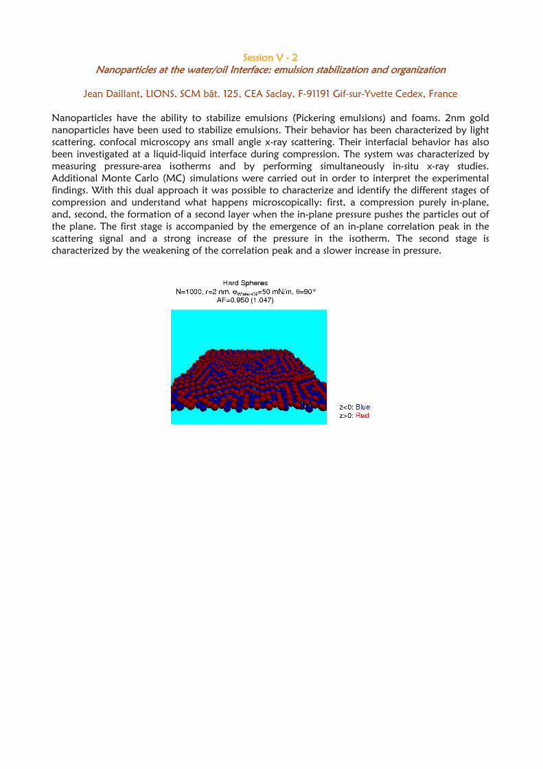
Session V - 2 Nanoparticles at the water/oil Interface: emulsion stabilization and organization
Jean Daillant, LIONS, SCM bât. 125, CEA Saclay, F-91191 Gif-sur-Yvette Cedex, France
Nanoparticles have the ability to stabilize emulsions (Pickering emulsions) and foams. 2nm gold nanoparticles have been used to stabilize emulsions. Their behavior has been characterized by light scattering, confocal microscopy ans small angle x-ray scattering. Their interfacial behavior has also been investigated at a liquid-liquid interface during compression. The system was characterized by measuring pressure-area isotherms and by performing simultaneously in-situ x-ray studies. Additional Monte Carlo (MC) simulations were carried out in order to interpret the experimental findings. With this dual approach it was possible to characterize and identify the different stages of compression and understand what happens microscopically: first, a compression purely in-plane, and, second, the formation of a second layer when the in-plane pressure pushes the particles out of the plane. The first stage is accompanied by the emergence of an in-plane correlation peak in the scattering signal and a strong increase of the pressure in the isotherm. The second stage is characterized by the weakening of the correlation peak and a slower increase in pressure.

Session V - 3 Interfaces in nanocrystalline zirconium based alloys
S. Neogy, R. Tewari, D. Srivastava, G. K. Dey and S. Banerjee
Materials Science Division, Bhabha Atomic Research Centre,
Trombay, Mumbai 400 085, India [email protected]
Nanocrystalline materials have been the subject matter of several investigations in recent
times because of their unusual properties. There are several techniques of producing nanocrystalline solids1. Crystallization of metallic glasses is an important route of producing nanocrystalline solids because the nanocrystal size can be easily controlled by this method2. The advent of bulk metallic glasses has opened up a new avenue of obtaining large solids having a nanocrystalline microstructure through the crystallization route3-5. The interfaces in nanocrystalline solids are important like in any other microstructure because of their very strong influence on the properties of the material. The nanograin boundary has been examined by many tools, which allow a direct or indirect insight into its structure6. The high-resolution transmission electron microscope (HREM) offers the possibility of observing these interfaces directly. Nanosized grains have been produced in Zr based bulk metallic glasses and rapidly solidified metallic glasses by crystallization. The various types of interfaces generated in these microstructures have been examined by high resolution transmission electron microscopy (HREM). The nanocrystals produced by the crystallization of Zr54.5Cu20Al10Ni8Ti7.5 and Zr52Ti6Al10Cu18Ni14 bulk glasses have been found to lie in the size range of 15 to 50 nm and comprised phases isostructural with tetragonal Zr2Cu and Zr2Ni. These observations are similar to those made by Xing et al7. HREM examination of nanograin boundaries showed the extension of the lattice fringes right up to the grain boundary. The lattice could be resolved simultaneously in some of the grains in view indicating that grain boundaries are parallel to low index planes in these grains8. Crystallographic defects like stacking fault and antiphase domain boundary could be noticed in many of the nanograins. Within the nanograin of Zr2Ni phase besides the fundamental lattice fringes a domain like structure could also be revealed. A number of faults could also be observed in this nanograin. A detailed analysis of these crystallographic faults has been carried out. The same alloys have been produced in the glassy state by rapid solidification. Crystallization of the rapidly solidified metallic glasses also led to the formation of nanocrystals where HREM examination revealed the presence of twins and twin-twin interaction.
1C. Suryanrayana, Int. Mat. Rev., 40 (1995) 41-64. 2G. K. Dey, R. T. Savalia, E. G. Baburaj, S. Banerjee, J. Mater. Res., 13 (1998) 504 - 517. 3A. Inoue, Mat. Sci. Eng., 304 A (2001) 1 – 10. 432. A. L. Greer, Nature, 368 (1994) 688-689. 534. A. L. Greer, Mater Sci Eng A, 304-306 (2001) 68-72. 6D. H. Ping, D. X. Li and H. Q. Ye, J. Mater. Sci. Lett., 14 (1995) 1536 - 1540. 7L.Q. Xing, J. Eckert, W. Loser, L. Schultz and D.M. Herlach, Philosophical Magazine A, 79 (1999) 1095-1108. 8D.B. Williams and C.B. Carter in “Transmission electron microscopy III”, (New York; Plenum Press) (1996) 459.

Session V - 4 Synthesis of functional oxide materials
Manipulating Morphology
Deepa Khushalani
Materials Chemistry Group, Department of Chemical Sciences, Tata Institute of Fundamental Research, Colaba, Mumbai- 400 005, India
[email protected] During the last decade or so, there has been a dramatic increase in the development of novel synthetic strategies for formation of structured materials which have features at the micron and sub-micron level. Routes involving the top-down or the bottom-up approach have provided a simple, versatile and cost-effective manner to form viable application based materials. One of the pivotal strategies of creating unique nanostructures available to a chemist is the use of templates to control the nucleation, growth and alignment of the inorganic crystals. Organic ‘scaffolding’ is employed such that it is able to exploit the principles of molecular recognition and site-specific interaction and therefore structure-direct, size-constrain and provide specific crystallographic orientation of growing nuclei. Potential organic scaffolds that are currently being studied are biologically derived amphiphiles, low molecular-weight surfactants (cationic, anionic, and neutral) and higher molecular-weight amphiphilic synthetic block co-polymers. The purpose of using such diversity of templating moieties is mainly to allow for improved interaction with the polymerizing/condensing inorganic building blocks and therefore to provide increased control of the resulting structure. The interaction between the organic scaffold and the inorganic building block can be either via hydrogen bonding, electrostatic or even through stronger linkages as ligation and direct covalent bonding. In addition, the deposition and growth of the inorganic replica is regulated by employing specific media such as organic gels or microemulsions. Presented here are some recent synthetic paradigms, under the umbrella of “soft condensed matter templating”, for growing a variety of inorganic structures. Furthermore, towards the aim of employing a synthetic approach to formation of functional materials (be they oxides, sulphides, phosphates etc), inevitably, researchers working the area of materials science tend to resort to commercially available reactive precursors for their synthesis. These are habitually alkoxide precursors as they afford simple, innocuous alcohol as by-products and the reagents are relatively easy to handle for either sol-gel synthesis for viable powders or spin-casting for thin film production. Recently, in our lab, we have been able to develop a generic, easy route to forming soluble, reactive precursors of a variety of elements such as titanium, zinc, bismuth, iron, vanadium and zirconium, all of which contain a simple polyol ligand. These ligands are facile in their formation; structures have now been elucidated and can function as sophisticated precursors for generation of functional ferroelectrics, multiferroics, semiconductors and catalysts. For this presentation, the details of their synthesis, characterization and use to produce advanced functional materials will also be detailed.

Session V - 5 Nanostructured Polymers and Composites for Applications
in Organic Photovoltaic Devices
R.Demadrille*,
F.Lincker, S.Berson, J.DeGirolamo, T.Jiu, D.Aldakov, P.Rannou, P.Reiss, B.Grévin, F.Chandezon, A.Pron.
UMR5819-SPrAM (CEA-CNRS-Univ.Grenoble I), CEA-DRFMC 17 rue des Martyrs 38054 Grenoble Cedex 9. (France)
S.Bailly, S.Guillerez, R.De Bettignies, CEA-DRT, INES, Savoie Technolac, BP 332, 50, avenue du lac Léman, 73377, le Bourget du Lac. (France)
corresponding author: R.Demadrille, [email protected]
Organic photovoltaic cells of nanostructured bulk-heterojunctions type, which consist of pi-conjugated polymers as electron donors and fullerenes as electron acceptors, are considered as very promising materials in view of their efficiency of ca. 4.4%, which has recently been achieved for P3HT/PCBM based devices. Further significant improvement in the cell performance is expected, provided that new polymers better matching the solar spectrum and more effectively converting the radiation to electricity are developed. In the first part of this lecture, we will discuss the synthesis and detailed characterization of new copolymers suitable for the use as active components of the organic solar cells. Their design is based on the concept of complementary conjugated chromophore units whose presence results in a significant extension of the absorption spectral range (typically up to 700nm). In particular we will describe new oligomers and regioregular alternate copolymers or terpolymers containing thienylene and fluorenone units. One of the advantages of these newly developed systems is the possibility of fine adjusting of the position and the width of their band gap either by appropriate substitution or by selecting an appropriate sequence of mers1. In the second part of the lecture we will discuss the use of the basic concepts of supramolecular chemistry for the fabrication of nanostructured molecular composites. We will present new strategies which can be applied for the preparation of nanostructured active layers in all organic2 and hybrid (organic/inorganic) solar cells containing semiconductor nanocrystals3. In addition to the synthetic part of the lecture, optical, electronic and self-organization properties of the composites will be described in detailed. Their performance in real devices of bulk-heterojunction configuration will also be discussed.
1. R. Demadrille, M. Firon, J.Leroy, P. Rannou, A. Pron, 15, Adv.Funct.Mater., (2005), 1547. 2. S. Berson, R. De Bettignies, S. Bailly, S. Guillerez, Adv.Func.Mater. 17. (2007) 1377 3. J. De Girolamo, P. Reiss, A. Pron, J.Phys.Chem.C (2008), 112, 8797.

Session VI - 1 MOCVD and CVD growth of compound semiconductor nanostructures
S. Bhunia
Saha Institute of Nuclear Physics
Kolkata, India [email protected]
Growth, characterization and application of semiconductor nanowires have drawn much attention in recent years. These structures are quasi one-dimensional in nature and could be modulated both longitudinally as well as radially by incorporating various functional elements into them. These functional structures, in combination with the unique quantum mechanical properties arising due to quantum confinement of the carriers in them, are considered to be the basic building blocks of nanowires on, InP, GaP and Si substrates employing Au nanoparticle assisted vapor-liquid-solid growth mechanism (Fig. 1). Nanowires grown on these substrates showed high structural quality and band edge photoluminescence with energy blue shift of the peak due to quantum confinement of the carriers. Finally I will report growth of InP nanowires on patterned Si substrates. Au nanoparticles were generated in the trenches of the pattern by in-situ thermal treatment under low energy electron microscope. Nanowires were then grown on the specific sites by MOCVD technique. In the second part of my talk, I will discuss our recent interesting results on CVD growth of ZnO nanostructures. ZnO have attracted lots of attention in recent years because of its large direct bandgap (3.37 eV) and free exciton binding energy (60 meV) at room temperature pertinent to use in optoelectronic and photovoltaic in the UV region of the spectrum. Also, due to its non-centrosymmetric hexagonal crystal structure and highly anisotropic growth behavior of different crystal directions, it can grow in different nanostructural form which is intriguing to crystal growth point of view. We have carried out systematic study to understand the influence of different controlling parameters of CVD on the growth of one dimensional ZnO nanowire structures. Various interesting structures, such as truncated icosahedrons, sphelurites, nanoflowers were obtained on the way of successful growth of ZnO nanowires (Fig.2). The nanowire structures could be arranged in a selforganized process to give three dimensional flower-like structures. The detailed optical and structural characterizations of the nanostructures were carried out and will be discussed.

Session VI - 2 Nucleation and growth mechanisms of multi-walled carbon nanotubes
application in material science
Mathieu Pinault, Célia Castro, Aurélien Gohier, Julien Glory, Michaël Helezen, Agnieszka Mierczynska, Sophie Barrau, Dominique Porterat,
Martine Mayne-L’Hermite, Cécile Reynaud
Laboratoire Francis Perrin CEA-CNRS URA 2453, DSM/IRAMIS/SPAM, CEA-Saclay, France
The excellent mechanical properties coupled with the high electrical and thermal conductivities of carbon nanotubes (CNTs) are the origin of greater consideration as a very promising nanomaterial. Such properties open up new avenues for a large variety of applications such as conductive materials, mechanical reinforcement, heat exchange devices, filtering [1-4], … The properties of nanotubes are strongly related to their characteristics such as their structure, size and arrangement. In this context, the motivation of the work presented here is to develop the synthesis of long and aligned multi-walled carbon nanotubes (A-CNTs) in order to subsequently take the benefit of such characteristics for the preparation of different types of materials (e.g. composites or membranes), nanofluids and sensors.
The aerosol-assisted catalytic chemical vapour deposition developed in LFP will be described [5]. This process enables to produce A-CNTs with a high catalytic yield and a high growth rate. MWNTs contain almost no by-products and their length can reach few mm. In order to get a better control of this synthesis process, nanotube growth mechanisms are studied from the aerosol precursors to the formation of aligned nanotube carpets. The approach is first, to study the initial stages of nanotube growth and second, to follow the chronology of nanotube growth during carpet formation. During the initial stages of growth, we demonstrate that catalyst nanoparticles are first formed on silicon substrate and are subsequently sites for nanotube growth through a base growth mechanism [6]. Then, we developed a sequential synthesis process giving rise to multilayered carpets of well aligned MWNTs. The analysis of these multi-layered carpets show that reactive Fe and C vapours are feeding continuously the substrate surface by diffusion through the whole carpet, and that nanotubes grow through a base-growth mechanism all along the formation of A-CNT carpets. Finally, we demonstrate the absolute need of the catalyst source for continuous growth of the carpet as well as for the growth of a new carpet at the base of a pre-existing one [5].
Regarding applications and, first of all, composites, two types of polymer-based composites according to the nanotube filler arrangement, either random or oriented in a unidirectional direction (1D), will be presented. Generally, their properties (electrical and mechanical) are strongly depending on the elaboration process [7]. Directly related to the 1D nanotube-based composite concept, it is possible to fabricate nanoporous membranes exhibiting a thickness of 100 to 200 �m, the hollow central channels of nanotubes constituting an aligned porous network. Through diffusion experiments, we will demonstrate that such membranes are permeable. Nanotube-based nanofluids (e.g. water-based suspensions of MWNT) can be prepared by dispersing the long A-CNTs in water based media. Measurements of their thermal properties reveal a significant enhancement of thermal conductivity as compared to water. MWNT weight content and length are found to play an important role on the thermal conductivity of nanofluids [8]. Finally, chemical resistive sensors were elaborated by dispersing A-CNTs and first results indicate the possibility to detect up to 25 ppb of chlorine which is very encouraging for future developments. References [1 - 4] J.K.W. Sandler et al., Polymer 44 (2003) 5893. E.T. Thostenson et al. , J. Phys. D 35 (2002) L77. J. A. Eastman, et al., Appl. Phys. Lett. 78, 718-720 (2001). B.J. Hinds, et al. Science, 303, 62, (2004) [5] M. Pinault, et al., Nano Lett., 5, 12, 2394-2398 (2005) [6] M. Pinault, et al. Carbon, 2005, 43, 2968-2976. [7] A. Mierczynska, et al., J. of App. Polymer Science, 2006. [8] J. Glory, et al. . J. Appl. Phys, 2008

Session VI - 3 SiNW : Growth, functionalization and applications
Yannick Coffinier, Gaelle Piret, Florian Lapierre, Phuong Nhung Nguyen, Vincent Thomy and
Rabah Boukherroub
Molecular Nanostructures and Devices Group, IEMN, CNRS, BP60069, Avenue Poincaré, 59652 Villeneuve d’Ascq (France)
Single-crystal silicon nanowires (SiNWs) have been the subject of extensive research in electronics, photonics, optoelectronics, sensing and other novel device applications. Here, I will present the synthesis of these nanostructures, their functionalization and some applications we’re developing in the laboratory. Silicon nanowires used in the present study were prepared by the so-called vapor-liquid-solid (VLS) mechanism. The fundamental of VLS process is based on metal catalyst directed chemical vapor deposition of silicon. Si nanowires were also synthesized by an aqueous electroless etching (EE) method. The technique is based on the galvanic displacement of Si by Ag+ to Ag0 reduction on the wafer surface. The reaction proceeds in an aqueous solution of AgNO3 and HF acid. Briefly, Ag+ reduces onto the Si wafer surface by injecting holes into the Si valence band and oxidizing the surrounding lattice, which is subsequently etched by HF. The initial reduction of Ag+ forms Ag nanoparticles on the wafer surface, thus delimiting the spatial extent of the oxidation and etching process. Further reduction of Ag+ occurs on the nanoparticles, not the Si wafer, which becomes the active cathode by electron transfer from the underlying wafer. These SiNW will be functionalized with different chemistries for different applications I’ll present suchs as: SiNW as inorganic matric for Desoprtion/Ionization of biomolecules for Mass spectrometry analysis SiNW as surface for electrowetting and digital actuation of droplets: Application to lab-on-chip. The last application of SiNW is the SiNW capping with silver nanoparticles for ultrasenstive SERS interface for detection of biomolecules.

Session VI - 4 Synthesis and grafting of n and p type σ-π-σ systems on substrates for molecular electronic applications.
Fabrice Moggia,a Bruno Jousselme,a Gaël Robert,b Nathalie Lidgi-Guigui,b Vincent Derycke,b Jean-
Philippe Bourgoinb and Serge Palacina
a) Laboratoire de Chimie des Surfaces et Interfaces, SPCSI
b) Laboratoire d’Electronique Moléculaire, SPEC (CNRS URA 2464) CEA-Saclay, 466, 91191 Gif-sur-Yvette Cedex, France.
Dinesh K. Aswal, J V. Yakhmi Technical Physics and Prototype Engineering Division, Bhabha Atomic Research Centre, Trombay,
Mumbai 400 085, India
The drive toward yet further miniaturization of silicon-based electronics has led to a revival of efforts to build devices with molecular-scale components. Self-assembly monolayer is a key concept in an important aspect of bottom-up approaches to Nanoelectronic to build active devices that can switch, store and retrieve information. It takes advantage of the size, the diversity, the quantum properties and the self-organization properties of organic molecules and their ease to the connection of the macroscopic world. In this general context, the collaboration between CEA-DAE and the ANR project "MEMO" (2005-2009) are devoted to study the integration of organic compounds in memories based on resonant tunnelling diodes (RTD) for hybrid molecular electronics. A proposed architecture of such molecular RTD device consists in a monolayer of σ-π-σ organic molecules sandwiched between two electrodes. The specific compounds present alkyl-chains acting as tunnel barriers, while a π-moiety acts as the potential well. The principle of this device is to bring a molecular level of the molecule in resonance with the Fermi level of an electrode to induce a negative differential resistance effect.
Hence, we will present the synthesis of several new σ-π-σ compounds with specific grafting functions with a Terthiophene or naphthalene tetracarboxydiimide cores. Different chemical or electrochemical strategies employed for grafting the self-assembled monolayers of thiols, alkenes or diazoniums salts on gold or on silicon terminated hydrogen will be reviewed as well as the morphology and the structural characterization of the grafted layers underwent by Infrared, contact angle, XPS, electrochemistry and STM. Also, the current-voltage (I-V) characteristics of the SAM devices along the direction vertical to substrate will be presented.

Session VI - 5 High-frequency behavior of CNT transistors
G. Dambrine
Molecular Nanostructures and Devices Group,
IEMN, CNRS, BP60069, Avenue Poincaré, 59652 Villeneuve d’Ascq (France) Since its discovery in 1991 Carbon NanoTubes (NTs) arouse an extensive research activity creating an extremely wide domain of applications in the field of materials but also of new class of electronics. NTs exhibit unusual physical, chemical, mechanical and electrical properties. Electrical characteristics of Single Wall carbon NanoTubes SWNTs such as electrons/holes motilities, long mean-free paths are favourable for high performance transistors performing high density of on-state current and transconductance. Besides, theoretical works showed the high potentiality of SWNTs in the high frequency (HF) range which in turn has generated an intensive study of NTs based transistors operating into multi-GHz regime. We will present the main results of high frequency Carbon-Nanotubes-based transistors fabricated by IEMN- CEA-IRAMIS-SPEC. In a first part, we will describe the technological process and secondly, we will discuss of the high frequency characterizations and electrical modelling of such devices.

Session VII - 1 Quantum Dots and Self-assembled Q.dots-DNA Hybrids for device
Interface and Biosensor Applications
S. N. Sahu Institute of Physics
Bhubaneswar 751006 e-mail : [email protected]
Semiconductor nanocrystals with size comparable to Bohr exciton radius exhibits size dependant structural, optical, electrical, thermodynamic and device properties. Such properties as a results of carrier confinement in different directions yield various applications in the areas of sensors, display devices and in nano- biotechnological applications. However, polydispercity and polycrystallinity in the semiconductor Nano- crystals limit their applications in various technologically important areas. On the contrary, biomolecules like DNA. with their sequence specificity and inherent electrostatic interaction with the cations are very useful as bio-templates to self-assemble and synthesize ordered nanoconstructs which find applications in biosensor/biomolecular recognition and imaging applications. With a motivation to study the above, we have synthesized various semiconductor nanostructure viz. CdS, CdSe, Porous Si, GaAs, PbS, HgS, and HgTe etc. CdS nanocrystals show UV sensor applications whereas the devices fabricated in the Schottky configuration show non ideal device behavior. The device interface states have been shown to be an important factor responsible for such non-ideal Schottky behavior as confirmed from devices fabricated using nanocrystals of CdSe, CdS and GaAs. Sequence specific semiconductor nanostructure-DNA hybrids(nanostars, nanobeads and nanowires) of HgTe and CdSe have been fabricated based on electrostatic interaction of DNA with multivalent cations leading to charge reversal process and then electrodeposition on a conducting substrate. Crystalline size and structure have been found to depend upon sequence specific properties of DNA as confirmed by the data analysis using different analytical tools. The DNA tag to the semiconductor nanocrystals as confirmed from FTIR measurements have resulted different optical properties viz. photoluminescence and optical absorption. Absorption quenching, red /blue shift as a result of DNA hybridization with semiconductor nanocrystals suggest that the technique can be very useful for biosensor applications compared to PCR based techniques.

Session VII - 2 Si Nanocrystals : Synthesis and functionnalization of for life science applications
V. Maurice, O. Sublemontier, O. Guillois, E. Doris*, N. Herlin-Boime
Service de Photons Atomes et Molécules, CEA/ DSM/IRAMIS/SPAM/LFP, CEA Saclay, 91191 Gif sur Yvette, France
* CEA/DSV/IBITECS, CEA Saclay, 91191 Gif sur Yvette, France [email protected]
Summary : Over the last years, the study of nanosized structures has become a very active field of research, due to the specific properties expected when the size is decreased down to the nanometric scale. Particular attention has been paid to the study of silicon quantum dots which are very attractive materials due to their photoluminescence (PL) emission that can be very strong at room temperature in the visible range under UV illumination. Weighable batches of high quality small Si nanocrystals (nc-Si) in terms of size control, purity and size distribution width are demanded for several applications in opto-electronic, photovoltaic, medicine, and so on. Nearly 10 years ago, CO2 laser pyrolysis of silane demonstrated its ability to produce light-emitting nc-Si with a very narrow size distribution with size in the range of few nanometers, but the production rate for the smallest particles was very low. Our work aimed to overcome this limitation. A precise size control of powders was obtained by way of CO2 laser pulse length adjustment while keeping the laser duty cycle and all the other synthesis parameters constant. This parameter can be considered as a new simple to use synthesis parameter for a fine size control of nc-Si in the 3-5 nm range with production rates of 200 mg/hour in this size range. For applications in the biomedical field, it is necessary to achieve stable colloidal solutions of non toxic, dispersed and highly photoluminescent nc-Si in bio-compatible media. Surface passivation and functionnalization are essential steps in order to achieve this aim. Results concerning the surface passivation in various liquid media and their consequences in terms of PL properties will be presented together with effects of grafting functions such as APTS (3-aminopropyltriéthoxysilane) at the surface. Information on the toxicity of these nanoparticles towards lung cells will also be given.

Session VII - 3 Nanoscale hybrid objects: from 3D Small angle neutron scattering study
to tunable 2D arrays formation
Géraldine Carrot CEA-Saclay- IRAMIS - Laboratoire Léon Brillouin
Nanohybrid objects based on polymer and inorganic nanoparticles are of great interest for
different reasons. Indeed, the polymer part can help first for the stability and the organization of the particles, second to increase the amount of chemical functions available in the organic corona and finally to improve or to mask the properties of the particles. SANS is a well-suited technique for the study of these objects particularly due to the possibility to use contrast matching to see either the particle or the polymer corona. Here we are interested in the synthesis of platinum nanoparticles grafted with polymers and/or biological molecules which may be used as probes for biological detection. Indeed, the combination of the catalytic properties of the platinum with the functionalities of the polymer makes these objects particularly attractive for this type of application.
The method to introduce the polymer consists in using both the "grafting from" technique and controlled radical polymerisation. These systems are exempt of free polymers so the characterization via SANS can lead to quantitative data such as the amount of chains in the polymer corona and the chains molecular weight. Contrast matching has been used to see only the polymer chains. In both cases, polymerization kinetics was followed by SANS and the polymer corona spectra show a plateau at small q which attests that the objects are individual and well-dispersed. We used different models to fit the form factor: corona or polymer star (chains connected together to a very small core) depending on the system. From these models, we can determine both the number of chains, the radius of gyration of the polymer corona and the chains molecular weight. Results obtained from SANS have been compared to other techniques such as NMR or TEM measurements. A good correlation has also been observed with the compression isotherms of Langmuir films obtained directly from the polymer-grafted nanoparticles. The next step is the characterization of the grafting of the proteins via activated ester based reaction.
Carrot G., El Harrak A., Oberdisse J., Jestin J., Boué F. Polymer grafting from 10-nm
individual particles: proving control by neutron scattering Soft Matter 2 (12): 1043-1047, 2006. Carrot G., Perez H. Controlled surface initiated polymerization from inorganic nanoparticles
Polymer Preprint: 827-828, 2006. G. Carrot, C. Cremona, F. Gal, J. Vinas, H. Perez, Polymer-grafted-platinum nanoparticles:
from 3D small-angle neutron scattering study to tunable 2D arrays formation, Langmuir (submitted)
Session VII - 4 Bottom-up approach for the elaboration of nanocomposite model structures
based organically capped platinum nanoparticles electrocatalyst
H.Perez1, B. Baret1, A. Etcheberry2
1- Laboratoire Francis Perrin, CEA/DSM/IRAMIS/SPAM-CNRS URA 2453, Bât. 522, 91191 Gif-sur-Yvette, France
2- Institut Lavoisier (IREM-CNRS, UMR 8637), Université de Versailles Saint Quentin en Yvelines, 45 avenue des Etats-Unis, 78035 Versailles Cedex, France
Platinum is still the reference material as electrocatalyst for oxygen reduction and hydrogen oxidation in Proton Exchange Membrane Polymer fuel Cells. The efficiency of the catalyst incorporated in the electrodes of fuel cells depends on the features of the catalyst itself (size and shape of the nanoparticules) and those of the active layer in which it is incorporated. With these respects the bottom-up approach which consists in pre-synthesizing nanoparticles with a known narrow size and shape distribution followed by their controlled organisation in an active layer is of particular interest. However, if such an approach can be found in the literature, most of the time an “activation step” (thermal or electrochemical) of the electrodes is performed before the evaluation of the performances of the electrocatalyst by electrochemistry or in real devices. Such treatments are performed to remove organic components present on the surface of the catalyst (for example the protecting shell which allowed the features of the nanoparticles to be controlled) and to measure an active surface area of the electrode related to the amount of catalyst. Such treatments actually modify the features of the catalyst and therefore reduce the interest of the bottom-up approach as a way to make model electrocatalyst structure. This paper presents our research on the synthesis and the study of organically capped platinum nanoparticles. These particles are synthesized from a mother functionalized particle which is further chemically derivatized in order to modify the features of the organic capping 1,2. The organization of these nanoparticles into solid nanostructures using the Langmuir-Blodgett method allows electrodes to be formed. The electrochemical activity of these structures can be studied without activation treatment 3 thus preserving the initial features of the catalyst. The evolution of the electrochemical responses can be studied as a function of parameters such as the environment of the nanoparticles or the amount of platinum involved 4.5. The interesting properties recorded on these original capped platinum catalysts led us to study the elaboration of porous nanocomposite electrodes by controlled combination with carbon nanotubes. The resulting electrodes can be viewed as model systems which can be characterized ex situ by cyclic voltammetry in a three-electrode cell and well as in situ in fuel cell devices. 1 Perez H., Pradeau J.P., Albouy P.-A.and Perez-Omil J, “Synthesis and Characterization of Functionalized Platinum Nanoparticles » Chem. Mater. 1999, 11, 3460-3463 2 Perez H., Noël V., Cavaliere-Jaricot S., §,†, Arnaud Etcheberry A., Pierre-Antoine Albouy P-A., “Nanocomposite LB films based on crown derivatized platinum nanoparticles: synthesis, characterization and electrical properties”, Thin solid films (in press) 3 Cavaliere S, Raynal F., Etcheberry,A., Herlem M. and Henri Perez H. “Direct Electrocatalytic Activity of Capped Platinum Nanoparticles toward Oxygen Reduction”, Electrochemical and Solid-State Letters, 7 10 A358-A360 2004 4 Cavaliere-Jaricot S, Etcheberry A., Noël V., Herlem M., Perez H. “Electronic transfer through Langmuir–Blodgett layers of capped platinum nanoparticles: An electrochemical approach”, Electrochimica Acta 51 (2006) 6076–6080 5 Cavaliere-Jaricot S., Haccoun J., Etcheberry A., Herlem M., Perez H. “Oxygen reduction of pre-synthesized organically capped platinum nanoparticles assembled in mixed Langmuir–Blodgett films: Evolutions with the platinum amount and leveling after fatty acid removal”, Electrochimica Acta 53 (2008) 5992–5999


![The Mechanism of the Interfacial Charge and Mass … Prussian Blue Analogues (PBAs)[13–15] electrochemically grown as thin films were used. Some of PBAs were also tested in organic](https://static.fdocuments.in/doc/165x107/5b0e3bd97f8b9a5d528b52d9/the-mechanism-of-the-interfacial-charge-and-mass-prussian-blue-analogues-pbas1315.jpg)