
Board Design Guide - startcev.spb.rustartcev.spb.ru/jz4725/Jz4730_Board_Design Guide_EN.pdf · This...
37
Ingenic ® Jz4730 Board Design Guide Revision: 1.0 Date: Feb. 2007
-
Upload
dinhkhuong -
Category
Documents
-
view
227 -
download
0
Transcript of Board Design Guide - startcev.spb.rustartcev.spb.ru/jz4725/Jz4730_Board_Design Guide_EN.pdf · This...
Ingenic® Jz4730Board Design Guide Revision: 1.0 Date: Feb. 2007

Ingenic Jz4730 Board Design Guide Copyright © Ingenic Semiconductor Co. Ltd 2007. All rights reserved. Release history
Date Revision Change Feb. 2007 1.0 First release
Disclaimer This documentation is provided for use with Ingenic products. No license to Ingenic property rights is granted. Ingenic assumes no liability, provides no warranty either expressed or implied relating to the usage, or intellectual property right infringement except as provided for by Ingenic Terms and Conditions of Sale. Ingenic products are not designed for and should not be used in any medical or life sustaining or supporting equipment. All information in this document should be treated as preliminary. Ingenic may make changes to this document without notice. Anyone relying on this documentation should contact Ingenicfor the current documentation and errata.
Ingenic Semiconductor Co., Ltd. Room 108, Information Center Block A Zhongguancun Software Park, 8 Dongbeiwang west Road, Haidian District, Beijing China, 100193 Tel: 86-10-82826661 Fax: 86-10-82825845 Http: //www.ingenic.cn

Content
Board Design Guide for Jz4730, Revision 1.0
Copyright® 2005-2007 Ingenic Semiconductor Co., Ltd. All rights reserved.
i
Content
1 Overview............................................................................................ 1
1.1 Introduction ............................................................................................................................. 1 1.2 Reference Platform ................................................................................................................. 1
2 Platform Stack-Up and Placement..................................................... 3
2.1 General Design Considerations.............................................................................................. 3 2.2 Nominal 4-Layer Board Stack-Up ........................................................................................... 3 2.3 PCB Technology Considerations ............................................................................................ 4
3 External Memory Interface Design Guidelines .................................. 7
3.1 Overview ................................................................................................................................. 7 3.2 Static Memory Interface .......................................................................................................... 7
3.2.1 Boot Memory ................................................................................................................... 7 3.2.2 SRAM/Flash Memory Connection................................................................................... 8 3.2.3 NAND Flash Connection ................................................................................................. 9 3.2.4 16-bit PC Card/CF Card Interface................................................................................. 10 3.2.5 Support IDE PIO Mode...................................................................................................11
3.3 SDRAM ................................................................................................................................. 12
4 AC97/I2S Design Guidelines ........................................................... 15
4.1 AC97 Implementation ........................................................................................................... 15 4.2 I2S Implementation ............................................................................................................... 16 4.3 Layout Guideline ................................................................................................................... 16
5 USB Design Guidelines ................................................................... 19
6 LCD Design Guidelines ................................................................... 21
7 Ethernet Design Guidelines ............................................................. 23
7.1 Jz4730 MII Connection ......................................................................................................... 23
8 Miscellaneous Peripheral Design Guidelines .................................. 25
8.1 SSI Design Guideline............................................................................................................ 25 8.2 UART/IrDA ............................................................................................................................ 26
8.2.1 UART Implementation ................................................................................................... 26 8.2.2 IrDA Implementation...................................................................................................... 26
8.3 I2C Bus ................................................................................................................................. 27 8.4 PWM ..................................................................................................................................... 28 8.5 GPIO ..................................................................................................................................... 28 8.6 Smart-Card ........................................................................................................................... 28

Content
Libra Development Board for Jz4730, Revision 1.0
Copyright® 2005-2007 Ingenic Semiconductor Co., Ltd. All rights reserved.
ii
8.7 RTC .......................................................................................................................................29 8.8 JTAG/Debug Port ..................................................................................................................29
9 Platform Clock Guidelines ................................................................31
10 Platform Power Guidelines...............................................................33
10.1 Digital Power Delivery and Decoupling .................................................................................33 10.2 Analog Power Delivery Decoupling.......................................................................................33

Overview
Board Design Guide for Jz4730, Revision 1.0
Copyright® 2005-2007 Ingenic Semiconductor Co., Ltd. All rights reserved.
1
1 Overview Jz4730 is a Multimedia Applications Processor designed by INGENIC®, which addresses the Mobile, Multimedia, Low power requirement electronic product. Jz4730 integrates a high performance 32-bits CPU, support many Embedded Operating Systems such as Linux™, WinCE™, etc. It also integrates SDRAM memory controller, MAC, LCD controller, AC’97/I2S controller, Camera controller, SCC, SD/MMC, I2C, USB1.1 Host/Device, four UARTs, IrDA, GPIO and so on.
1.1 Introduction This design guide provides recommendations for system designs based on the Jz4730 processor. Design issues (e.g., thermal considerations) should be addressed using specific design guides or application notes for the processor. The design guidelines in this document are used to ensure maximum flexibility for board designers while reducing the risk of board related issues. The design information provided in this document falls into two categories:
• Design Recommendations: Items based on INGENIC’s simulations and lab experience to date and are strongly recommended, if not necessary, to meet the timing and signal quality specifications.
• Design Considerations: Suggestions for platform design that provide one way to meet the design recommendations. Design considerations are based on the reference platforms designed by INGENIC. They should be used as an example, but may not be applicable to particular designs.
Note: In this manual, processor means the Jz4730 processor if not specified. The guidelines recommended in this manual are based on experience and simulation work completed by INGENIC while developing systems with Jz4730. This work is ongoing, and the recommendations and considerations are subject to change. Platform schematics can be obtained and are intended as a reference for board designers. While the schematics may cover a specific design, the core schematics remain the same for most platforms. The schematic set provides a reference schematic for each platform component, and common system board options. Additional flexibility is possible through other permutations of these options and components.
The document can help customer span doorstep, design product using existent software and
hardware resources. Your advice is the best encourage for us.
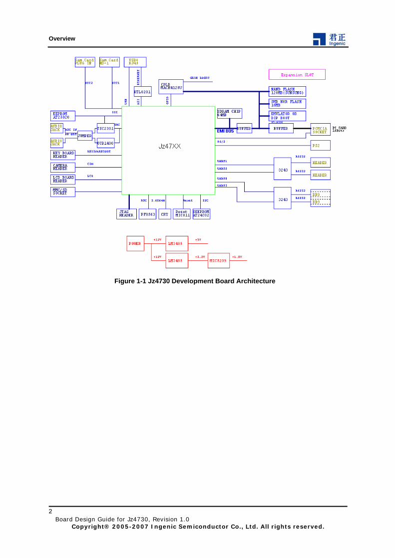
1.2 Reference Platform Figure 1-1 shows the Jz4730 Development Board Architecture.
Overview
Figure 1-1 Jz4730 Development Board Architecture
Board Design Guide for Jz4730, Revision 1.0 Copyright® 2005-2007 Ingenic Semiconductor Co., Ltd. All rights reserved.
2
Platform Stack-Up and Placement
2 Platform Stack-Up and Placement In this section, an example of a Jz4730 platform component placement and stack-up is presented for a PMP product.
2.1 General Design Considerations This section describes motherboard layout and routing guidelines for Jz4730 platforms. This section does not describe the functional of any bus, or the layout guidelines for an add-in device. If the guidelines listed in this manual are not followed, it is very important that thorough signal integrity and timing simulations are completed for each design. Even when the guidelines are followed, critical signals are recommended to be simulated to ensure proper signal integrity and flight time. Any deviation from the guidelines should be simulated. The trace impedance typically noted (i.e., 60Ω ± 15%) is the nominal trace impedance for a 5-mil wide trace. That is, the impedance of the trace when not subjected to the fields created by changing current in neighboring traces. When calculating flight times, it is important to consider the minimum and maximum impedance of a trace based on the switching of neighboring traces. Using wider spaces between the traces can minimize this trace-to-trace coupling. In addition, these wider spaces reduce settling time. Coupling between two traces is a function of the coupled length, the distance separating the traces, the signal edge rate, and the degree of mutual capacitance and inductance. To minimize the effects of trace-to-trace coupling, the routing guidelines documented in this section should be followed. Additionally, these routing guidelines are created using a PCB stack-up similar to that illustrated in Figure 2-1
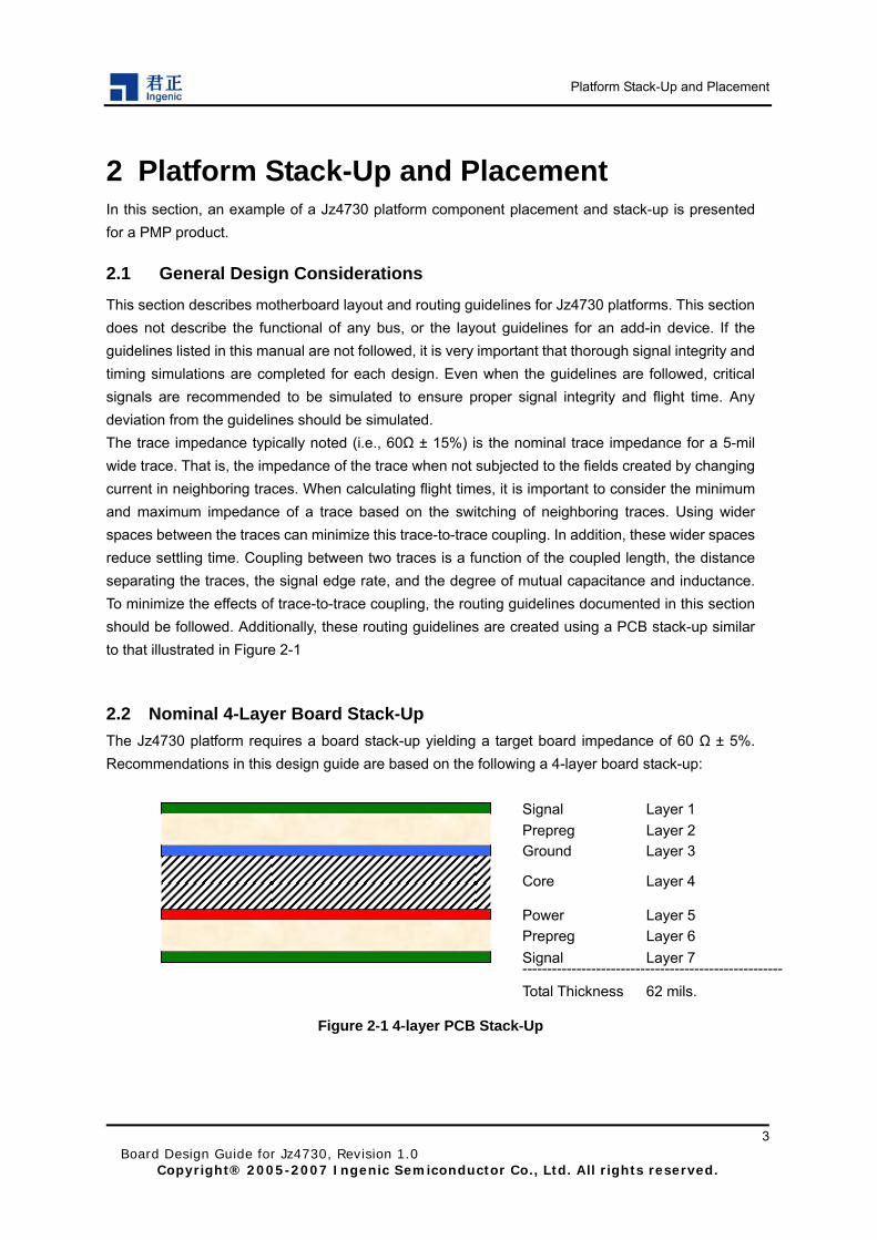
2.2 Nominal 4-Layer Board Stack-Up The Jz4730 platform requires a board stack-up yielding a target board impedance of 60 Ω ± 5%. Recommendations in this design guide are based on the following a 4-layer board stack-up:
Prepreg Layer 6
Ground Layer 3
Signal Layer 1 Prepreg Layer 2
Core Layer 4
Signal Layer 7 ----------------------------------------------------- Total Thickness 62 mils.
Power Layer 5
Figure 2-1 4-layer PCB Stack-Up
Board Design Guide for Jz4730, Revision 1.0
Copyright® 2005-2007 Ingenic Semiconductor Co., Ltd. All rights reserved.
3

Platform Stack-Up and Placement
Table 2-1 PCB Parameter
Description Nominal Value Tolerance Comments
Board Impedance Z0 60Ω ± 15% With nominal 5 mil trace width Dielectric Thickness 4.3 mils ± 0.5 mils 1 x 2116 Pre-Preg
Micro-stripline Er 4.1 ± 0.4 @ 100 MHz Trace Width 5.0 mils ± 0.5 mils Standard trace
Trace Thickness 2.1 mils ± 0.5 mils 0.5 oz foil + 1.0 oz plate Soldermask Er 4.0 ± 0.5 @ 100 MHz
Soldermask Thickness 1.0 mils ± 0.5 mils From top of trace
2.3 PCB Technology Considerations The following recommendation aids in the design of a Jz4730 based platform. Simulations and reference platform are based on the following technology, and we recommend that designers adhere to these guidelines.
Board Design Guide for Jz4730, Revision 1.0 Copyright® 2005-2007 Ingenic Semiconductor Co., Ltd. All rights reserved.
4
L1 Copper (pad)
L4
Finished Hole L2
Copper
Anti-Pad L3
Copper
Figure 2-2 PCB Technologies – Stack-Up

Platform Stack-Up and Placement
Board Design Guide for Jz4730, Revision 1.0
Copyright® 2005-2007 Ingenic Semiconductor Co., Ltd. All rights reserved.
5
Table 2-2 PCB Parameter for Vias
Number of Layers
Stack Up 4 Layer Cu Thickness 0.5 oz Outer (before plating); 1oz inner
Final Board Thickness 62 mils (- 5mils / +8mils) Material Fiberglass made of FR4
Signal and Power Via Stack Via Pad 26 mils
Via Anti-Pad 40 mils Via Finished Hole 14 mils

External Memory Interface Design Guidelines
Board Design Guide for Jz4730, Revision 1.0
Copyright® 2005-2007 Ingenic Semiconductor Co., Ltd. All rights reserved.
7
3 External Memory Interface Design Guidelines
The External Memory Controller (EMC) divides the off-chip memory space and outputs control signals complying with specifications of various types of memory and bus interfaces. It enables the connection of static memory, NAND flash memory, synchronous DRAM, etc., to this processor. It also supports the PCMCIA interface. This section is the design guidelines for the external memory interface.
3.1 Overview
3.2 Static Memory Interface The static memory controller provides a glue less interface to ROM, Burst ROM, SRAM, NOR Flash and NAND Flash. It support 6 chip selection CS5~0# and each bank can be configured separately. NAND flash interface is provided on CS3, sharing with static memory bank 3. Jz4730 support most types of NAND flashes, including 8-bit and 16-bit bus width, 512B and 2KB page size. It also support boot from NAND flash. The data bus width for each chip select region may be programmed to be 8-bit, 16-bit or 32-bit.
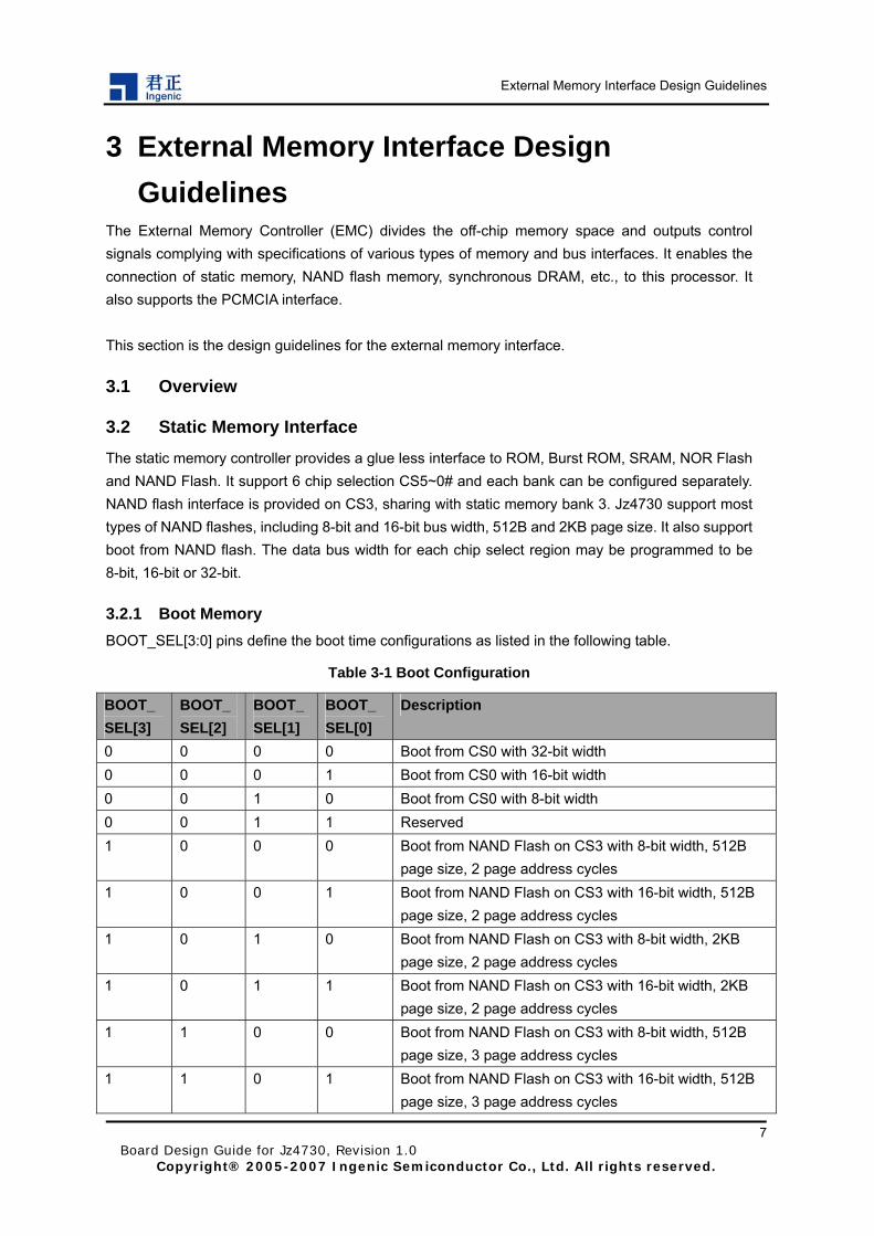
3.2.1 Boot Memory BOOT_SEL[3:0] pins define the boot time configurations as listed in the following table.
Table 3-1 Boot Configuration
BOOT_ SEL[3]
BOOT_ SEL[2]
BOOT_ SEL[1]
BOOT_ SEL[0]
Description
0 0 0 0 Boot from CS0 with 32-bit width 0 0 0 1 Boot from CS0 with 16-bit width 0 0 1 0 Boot from CS0 with 8-bit width 0 0 1 1 Reserved 1 0 0 0 Boot from NAND Flash on CS3 with 8-bit width, 512B
page size, 2 page address cycles 1 0 0 1 Boot from NAND Flash on CS3 with 16-bit width, 512B
page size, 2 page address cycles 1 0 1 0 Boot from NAND Flash on CS3 with 8-bit width, 2KB
page size, 2 page address cycles 1 0 1 1 Boot from NAND Flash on CS3 with 16-bit width, 2KB
page size, 2 page address cycles 1 1 0 0 Boot from NAND Flash on CS3 with 8-bit width, 512B
page size, 3 page address cycles 1 1 0 1 Boot from NAND Flash on CS3 with 16-bit width, 512B
page size, 3 page address cycles

External Memory Interface Design Guidelines
1 1 1 0 Boot from NAND Flash on CS3 with 8-bit width, 2KB page size, 3 page address cycles
1 1 1 1 Boot from NAND Flash on CS3 with 16-bit width, 2KB page size, 3 page address cycles
When boot from CS0, BOOT_SEL[1:0] is used to define the memory width which can be 8,16 or 32 bits. When boot from NAND flash, the data width of static memory bank 3 is defined by BOOT_SEL[0] pins which can be 8 or 16 bits. Data width of other static memory banks can be configured to 8, 16 or 32 bits by software.
3.2.2 SRAM/Flash Memory Connection
Chip Select
Address
Write Enable
Read Enable
Data
ADD[n:0]
CS[n]#
RD#
WE#
Data[7:0]
A[n:0]
CS#
OE#
WE#
I/O [7:0]
Jz4730 SRAM/Flash
Figure 3-1 8-bit SRAM/Flash Interconnection Example
Board Design Guide for Jz4730, Revision 1.0 Copyright® 2005-2007 Ingenic Semiconductor Co., Ltd. All rights reserved.
8
External Memory Interface Design Guidelines
Board Design Guide for Jz4730, Revision 1.0
Copyright® 2005-2007 Ingenic Semiconductor Co., Ltd. All rights reserved.
9
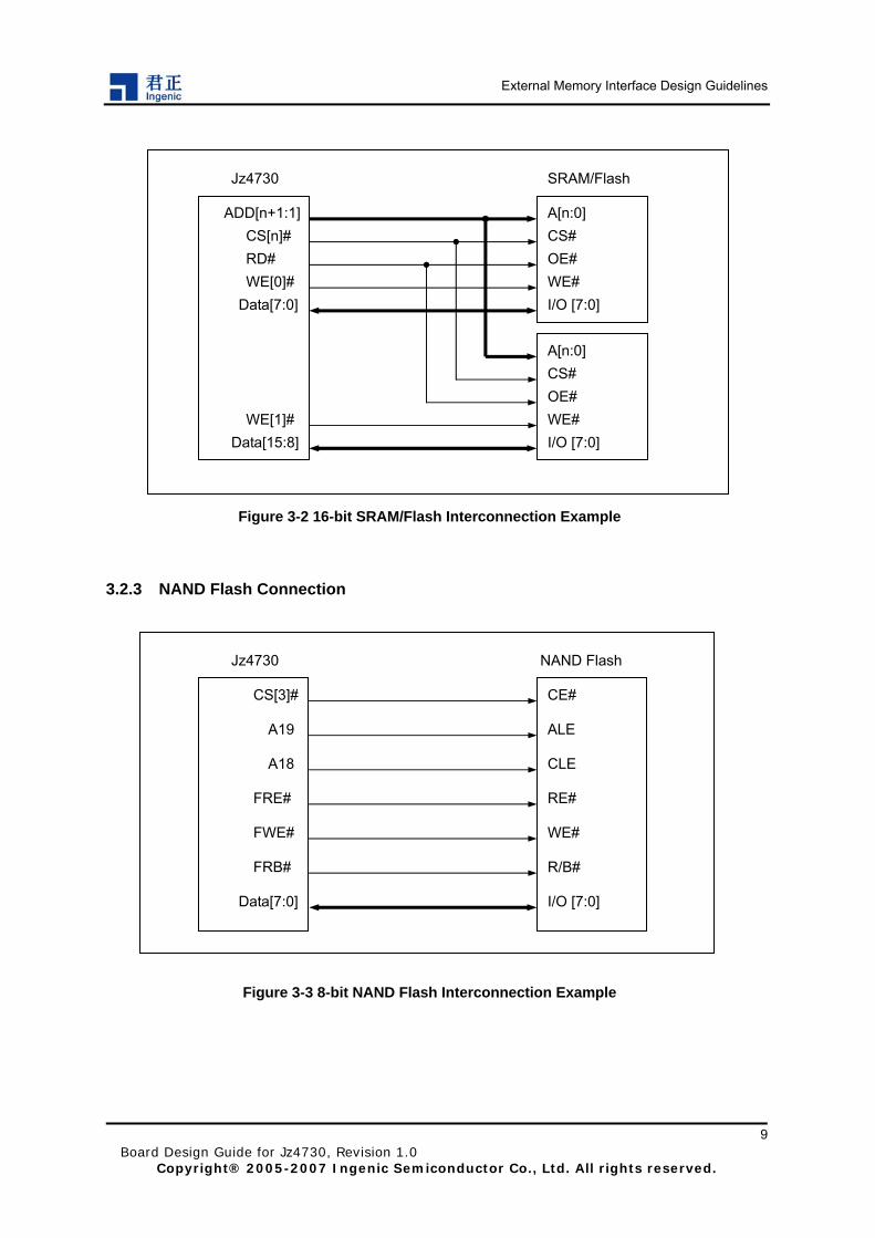
Figure 3-2 16-bit SRAM/Flash Interconnection Example
3.2.3 NAND Flash Connection
A[n:0] CS# OE# WE# I/O [7:0]
SRAM/Flash
A[n:0] CS# OE# WE# I/O [7:0]
ADD[n+1:1] CS[n]# RD# WE[0]#
Data[7:0]
Jz4730
Data[15:8] WE[1]#
CS[3]#
A19
A18
Data[7:0]
Jz4730
FRE#
FWE#
FRB#
CE#
ALE
CLE
I/O [7:0]
NAND Flash
RE#
R/B#
WE#
Figure 3-3 8-bit NAND Flash Interconnection Example

External Memory Interface Design Guidelines
3.2.4 16-bit PC Card/CF Card Interface
A[25::0]
REG#
D[15::0]
CE[2::1]#
OE#
WE#
IORD#
IOWR#
CD1
CD2
VS1#
VS2#
RESET
WAIT#
Socket
IOIS16#
DIR OE#
Jz4730
A[25::0]
PREG#
D[15::0]
PCE1#
PCE2#
WAIT#
IOIS16#
RD#
WE#
WE0/IOW#
WE1/IOR#
RD/WR#
GPIO[n]
GPIO[n]
GPIO[n]
GPIO[n]
GPIO[n]
GPIO[n]
Figure 3-4 16-bit PC Card Interconnection Example
Board Design Guide for Jz4730, Revision 1.0 Copyright® 2005-2007 Ingenic Semiconductor Co., Ltd. All rights reserved.
10

External Memory Interface Design Guidelines
3.2.5 Support IDE PIO Mode Socket Jz4730
Board Design Guide for Jz4730, Revision 1.0
Copyright® 2005-2007 Ingenic Semiconductor Co., Ltd. All rights reserved.
11
HD_A[2::0]
D[15::0]
HD_CS0#
HD_CS1#
OE#
WE#
IORD#
IOWR#
CD1
CD2
VS1#
VS2#
RESET
WAIT#
IOIS16#
DIR OE#
D[15::0]
RD/WR#
A[3::1]
HD_CS0#
HD_CS1#
RD#
WE#
WE0/IOW#
WE1/IOR#
IOIS16#
WAIT#
GPIO[n]
GPIO[n]
GPIO[n]
GPIO[n]
GPIO[n]
External Memory Interface Design Guidelines
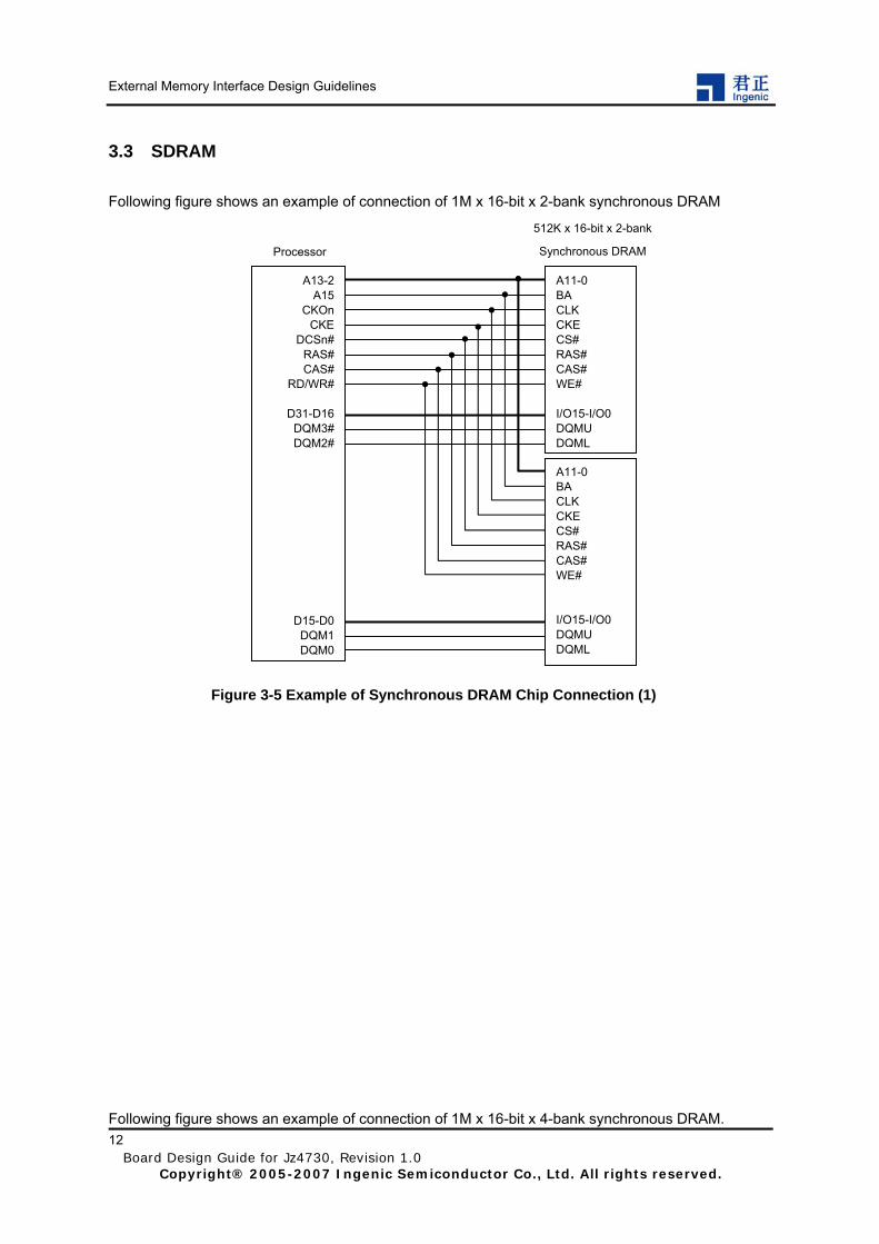
3.3 SDRAM Following figure shows an example of connection of 1M x 16-bit x 2-bank synchronous DRAM
A13-2 A15
CKOn CKE
DCSn# RAS# CAS#
RD/WR#
D31-D16 DQM3# DQM2#
D15-D0 DQM1 DQM0
A11-0 BA CLK CKE CS# RAS# CAS# WE# I/O15-I/O0 DQMU DQML
Processor
512K x 16-bit x 2-bank
Synchronous DRAM
A11-0 BA CLK CKE CS# RAS# CAS# WE# I/O15-I/O0 DQMU DQML
Figure 3-5 Example of Synchronous DRAM Chip Connection (1)
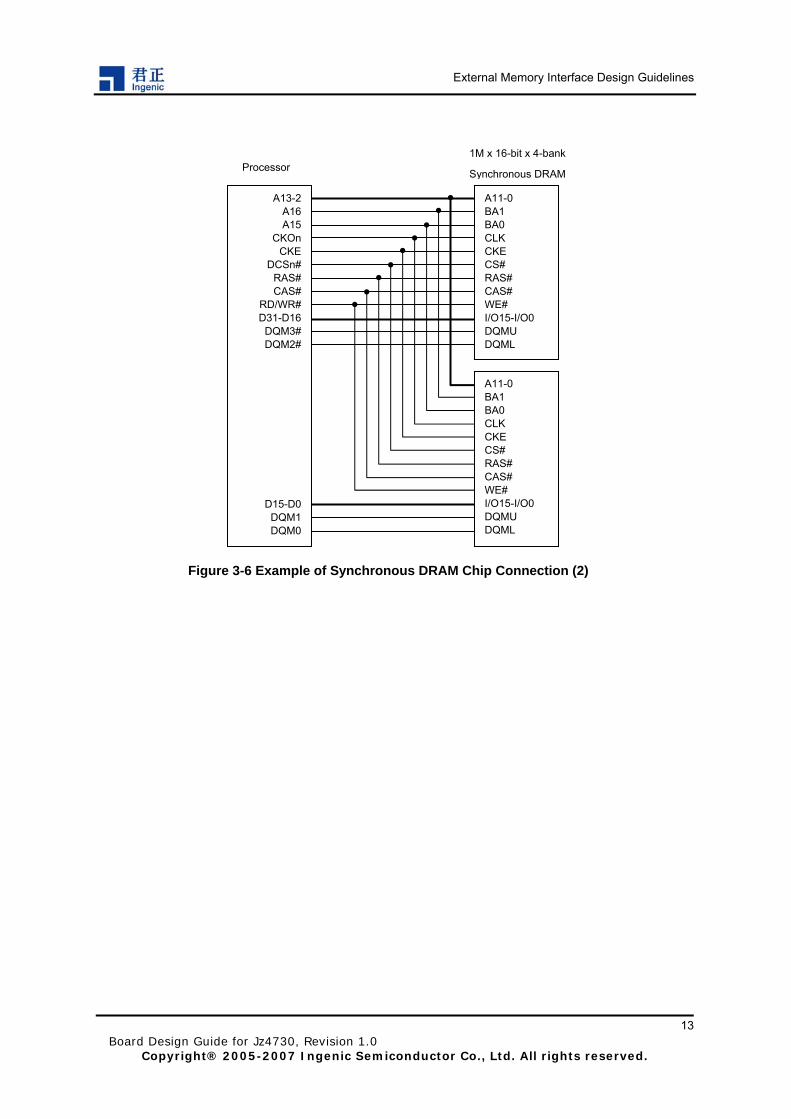
Following figure shows an example of connection of 1M x 16-bit x 4-bank synchronous DRAM.
Board Design Guide for Jz4730, Revision 1.0 Copyright® 2005-2007 Ingenic Semiconductor Co., Ltd. All rights reserved.
12
External Memory Interface Design Guidelines
A11-0 BA1 BA0 CLK CKE CS# RAS# CAS# WE# I/O15-I/O0 DQMU DQML
Processor 1M x 16-bit x 4-bank
Synchronous DRAM
A11-0 BA1 BA0 CLK CKE CS# RAS# CAS# WE# I/O15-I/O0 DQMU DQML
A13-2 A16 A15
CKOn CKE
DCSn# RAS# CAS#
RD/WR# D31-D16
DQM3# DQM2#
D15-D0 DQM1 DQM0
Figure 3-6 Example of Synchronous DRAM Chip Connection (2)
Board Design Guide for Jz4730, Revision 1.0
Copyright® 2005-2007 Ingenic Semiconductor Co., Ltd. All rights reserved.
13


AC97/I2S Design Guidelines
4 AC97/I2S Design Guidelines The AIC(AC’97 and I2S Controller) of Jz4730 supports the Audio Codec '97 Component Specification 2.3 for AC-link format and I2S or IIS (for inter-IC sound), a protocol defined by Philips Semiconductor. Both normal I2S and the MSB-justified I2S formats are supported by AIC. The AC-link is a synchronous, fixed-rate serial bus interface for transferring CODEC register control and status information in addition to digital audio. Where both normal I2S and MSB-justified-I2S work with a variety of clock rates, which can be obtained either by dividing the PLL clock by two programmable dividers or from an external clock source. For I2S systems that support the L3 control bus protocol, additional pins are required to control the external CODEC. CODECs that use an L3 control bus require 3 signals: L3_CLK, L3_DATA, and L3_MODE for writing bytes into the L3 bus register. The AIC supports the L3 bus protocol via software control of the general-purpose I/O (GPIO) pins. The AIC does not provide hardware control for the L3 bus protocol. The AC’97 interface and I2S interface can’t be used at the same time, and if the AIC function is disabled, its pins may be used for GPIO functions.
4.1 AC97 Implementation The AC-link is a bi-directional, serial PCM digital stream. It handles multiple input and output data streams, as well as control register accesses, employing a time division multiplexed (TDM) scheme. The AC-link architecture provides for data transfer through individual frames transmitted in a serial fashion. Each frame is divided into 12 outgoing and 12 incoming data streams, or slots.
Jz4730 AC’97 CODEC
AC_RST#
AC_SYNC
AC_DOUT
AC_DIN
BIT_CLK 33Ω
Figure 4-1 AC-Link Interconnection
Board Design Guide for Jz4730, Revision 1.0
Copyright® 2005-2007 Ingenic Semiconductor Co., Ltd. All rights reserved.
15

AC97/I2S Design Guidelines
4.2 I2S Implementation The following figure shows an connection example between Jz4730 and I2S Codec. The I2S Codec is a Master device and Jz4730 is a Slave device. MCLK is the master clock input for I2S Codec. For details please refer to the document: AN4730_002_i2s.pdf
SYNC
DOUT
DIN
BIT_CLK
SCC1 CLK
GPIO
Jz4730(Slave) I2S Codec(Master)
I2S_LRCLK
I2S_DIN
I2S_DOUT
I2S_BCLK
MCLK
L3 (Optional)
Figure 4-2 I2S Interconnection
4.3 Layout Guideline Using the assumed 4-layer stack-up, the AC97/I2S interface can be routed using 5 mil traces with 5-mil spacing between the traces. Maximum length between Jz4730 to CODEC is 15 inches. Trace impedance should be Z0 = 60 Ω ± 15%. To ensure the maximum performance of the codec, proper component placement and routing techniques are required. These techniques include properly isolating the codec, associated audio circuitry, analog power supplies, and analog ground planes, from the rest of the motherboard. This includes plane splits and proper routing of signals not associated with the audio section. Contact your vendor for device-specific recommendations. The basic recommendations are as follows:
• Special consideration must be given for the ground return paths for the analog signals. • Digital signals routed in the vicinity of the analog audio signals must not cross the power
plane split lines. Analog and digital signals should be located as far as possible from each other.
• Partition the board with all analog components grouped together in one area and all digital components in another.
• Separate analog and digital ground planes should be provided, with the digital components over the digital ground plane, and the analog components, including the analog power regulators, over the analog ground plane. The split between planes must be a minimum of 0.05 inch wide.
Board Design Guide for Jz4730, Revision 1.0 Copyright® 2005-2007 Ingenic Semiconductor Co., Ltd. All rights reserved.
16

AC97/I2S Design Guidelines
Board Design Guide for Jz4730, Revision 1.0
Copyright® 2005-2007 Ingenic Semiconductor Co., Ltd. All rights reserved.
17
• Keep digital signal traces, especially the clock, as far as possible from the analog input and voltage reference pins.
• Do not completely isolate the analog/audio ground plane from the rest of the board ground plane. There should be a single point (0.25 inch to 0.5 inch wide) where the analog/isolated ground plane connects to the main ground plane. The split between planes must be a minimum of 0.05 inch wide.
• Any signals entering or leaving the analog area must cross the ground split in the area where the analog ground is attached to the main motherboard ground. That is, no signal should cross the split/gap between the ground planes, which would cause a ground loop, thereby greatly increasing EMI emissions and degrading the analog and digital signal quality.
• Analog power and signal traces should be routed over the analog ground plane. • Digital power and signal traces should be routed over the digital ground plane. • Bypassing and decoupling capacitors should be close to the IC pins, or positioned for the
shortest connections to pins, with wide traces to reduce impedance. • All resistors in the signal path or on the voltage reference should be metal film. Carbon
resistors can be used for DC voltages and the power supply path, where the voltage coefficient, temperature coefficient, and noise are not factors.
• Regions between analog signal traces should be filled with copper, which should be electrically attached to the analog ground plane. Regions between digital signal traces should be filled with copper, which should be electrically attached to the digital ground plane.
• Locate the crystal or oscillator close to the codec.


USB Design Guidelines
Board Design Guide for Jz4730, Revision 1.0
Copyright® 2005-2007 Ingenic Semiconductor Co., Ltd. All rights reserved.
19
5 USB Design Guidelines Jz4730 integrates USB Host Controller (UHC), which is Open Host Controller Interface (OHCI)-compatible and USB Revision 1.1-compatible. It supports both low-speed (1.5 Mbps) and full-speed (12 Mbps) USB devices. Two downstream ports are provided. Jz4730 also integrates USB device controller (UDC), which is USB Revision 1.1-compliant full-speed device. Note: USB device port is multiplexed with USB host port 0 and is selected by SBA_CNTL.USBCFG register. The following are general guidelines for the USB interface:
• Unused USB ports should be terminated with 15 kΩ pull-down resistors on both D+/D- data lines.
• 15 Ω series resistors should be placed as close as possible to the Jz4730. These series resistors provide source termination of the reflected signal.
• 47-pF caps must be placed as close as possible to the Jz4730 as well as on the processor side of the series resistors on the USB data lines (D0±, D1±). These caps are for signal quality (rise/fall time) and to help minimize EMI radiation.
• 15 kΩ ± 5% pull-down resistors should be placed on the USB side of the series resistors on the USB data lines (D0±, D1±). They provide the signal termination required by the USB specification. The stub should be as short as possible.
• The trace impedance for the D0± and D1± signals should be 45 Ω (to ground) for each USB signal D+ or D-. This may be achieved with 9-mil-wide traces on the motherboard based on the stack-up recommended in Figure 3-1. The impedance is 90 Ω between the differential signal pairs D+ and D-, to match the 90 Ω USB twisted-pair cable impedance. Note that the twisted-pair characteristic impedance of 90 Ω is the series impedance of both wires, which results in an individual wire presenting 45Ω impedance. The trace impedance can be controlled by carefully selecting the trace width, trace distance from power or ground planes, and physical proximity of nearby traces.
• USB data lines should be routed as ‘critical signals’. (i.e., hand-routing preferred). The D+/D- signal pair should be routed together and not parallel to other signal traces, to minimize cross-talk. Doubling the space from the D+/D- signal pair to adjacent signal traces will help to prevent cross-talk. The D+/D- signal traces should also be the same length, which will minimize the effect of common mode current on EMI.

USB Design Guidelines
45 Ω
Driver
D+
Driver
D-
Motherboard Trace
Motherboard Trace
45 Ω
90 Ω
15 Ω
15 kΩ 47 pF
15 Ω
15 kΩ 47 pF
USB
Con
nect
or
Jz4730 Transmission Line USB Twisted-pair Cable
Figure 5-1 Recommend USB Host Schematic
Jz4730 Transmission Line USB Twisted-pair Cable
45 Ω
Driver
D+
Driver
D-
Motherboard Trace
Motherboard Trace
45 Ω
90 Ω
15 Ω
1.5 kΩ
47 pF
15 Ω
47 pF
USB
Con
nect
or
VCC
Figure 5-2 Recommend USB Device Schematic
Board Design Guide for Jz4730, Revision 1.0 Copyright® 2005-2007 Ingenic Semiconductor Co., Ltd. All rights reserved.
20

LCD Design Guidelines
6 LCD Design Guidelines The Jz4730 integrated LCD controller has the capabilities to driving the latest industry standard STN and TFT LCD panels. It also supports some special TFT panels used in consuming electronic products. The controller performs the basic memory based frame buffer and palette buffer to LCD panel data transfer through use of a dedicated DMA controller.
PCLK VSYNC HSYNC R7 R6 R5 R4 R3 R2 R1 R0 G7 G6 G5 G4 G3 G2 G1 G0 B7 B6 B5 B4 B3 B2 B1 B0 DE Other Signal
LCD Module
PCLK VSYNC HSYNC D[15] D[14] D[13] D[12] D[11] D[10] D[9] D[8] D[7] D[6] D[5] D[4] D[3] D[2] D[1] D[0] DE Other Signal
Jz4730
Figure 6-1 24-bit LCD Module Connection Example
Board Design Guide for Jz4730, Revision 1.0
Copyright® 2005-2007 Ingenic Semiconductor Co., Ltd. All rights reserved.
21


Ethernet Design Guidelines
7 Ethernet Design Guidelines The Jz4730 processor contains one Ethernet media access controller (MAC) that supporting 10/100Mbps Ethernet. The MAC provides the interface between the host application and the PHY layer through the media independent interface (MII). The PHY layer device is external to the processor. This section describes design guidelines for the LAN on board based Jz4730.
Jz4730 Magnetic Module
Phyceiver ConnectorMII
Figure 7-1 LAN On Board Implementation
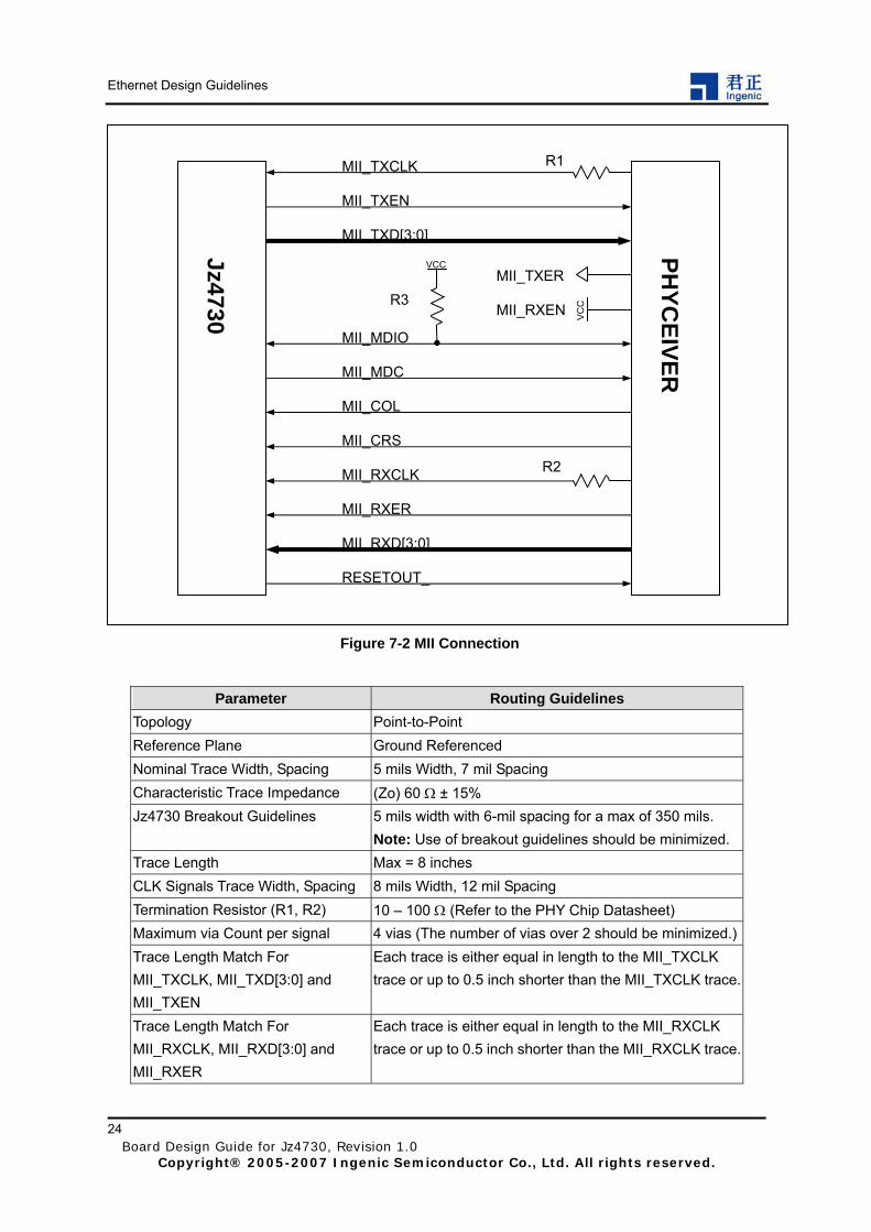
7.1 Jz4730 MII Connection Jz4730 MII interconnection example is shown as figure 7-2, the Ethernet PHY chip maybe varied for specific OEM design targets. Two source termination resistors (R1, R2) are recommended for better signal integrity for the two clock signals (MII_TXCLK and MII_RXCLK, 25MHz at 100M LAN), the value of R1 and R2 maybe 33 Ω (refer to the PHY chip datasheet) to compensate for minor the difference between the chip output and PCB trace impedance. The R1 and R2 should be placed as close as possible to the PHY chip. R3 is a 1.5K Ω pull-up resistor because the signal MII_MDIO is an open-drain pad for most phyceiver chip. Jz4730 RESETOUT_ drive the RESET# input to reset the PHY chip when power-up.
Board Design Guide for Jz4730, Revision 1.0
Copyright® 2005-2007 Ingenic Semiconductor Co., Ltd. All rights reserved.
23
Ethernet Design Guidelines
MII_TXEN
MII_TXD[3:0]
MII_COL
MII_CRS
MII_MDC
MII_MDIO
MII_RXER
MII_RXD[3:0]
RESETOUT_
Jz4730
PHYC
EIVER
MII_TXCLK R1
MII_TXER
MII_RXEN VC
C
VCC
R3
MII_RXCLK R2
Figure 7-2 MII Connection
Parameter Routing Guidelines
Topology Point-to-Point Reference Plane Ground Referenced Nominal Trace Width, Spacing 5 mils Width, 7 mil Spacing Characteristic Trace Impedance (Zo) 60 Ω ± 15% Jz4730 Breakout Guidelines 5 mils width with 6-mil spacing for a max of 350 mils.
Note: Use of breakout guidelines should be minimized.Trace Length Max = 8 inches CLK Signals Trace Width, Spacing 8 mils Width, 12 mil Spacing Termination Resistor (R1, R2) 10 – 100 Ω (Refer to the PHY Chip Datasheet) Maximum via Count per signal 4 vias (The number of vias over 2 should be minimized.)Trace Length Match For MII_TXCLK, MII_TXD[3:0] and MII_TXEN
Each trace is either equal in length to the MII_TXCLK trace or up to 0.5 inch shorter than the MII_TXCLK trace.
Trace Length Match For MII_RXCLK, MII_RXD[3:0] and MII_RXER
Each trace is either equal in length to the MII_RXCLK trace or up to 0.5 inch shorter than the MII_RXCLK trace.
Board Design Guide for Jz4730, Revision 1.0 Copyright® 2005-2007 Ingenic Semiconductor Co., Ltd. All rights reserved.
24

Miscellaneous Peripheral Design Guidelines
8 Miscellaneous Peripheral Design Guidelines 8.1 SSI Design Guideline The SSI is a full-duplex synchronous serial interface and can connect to a variety of external analog-to-digital (A/D) converters, audio and telecom codecs, and other devices that use serial protocols for transferring data. The SSI supports National’s Microwire, Texas Instruments Synchronous Serial Protocol (SSP), and Motorola’s Serial Peripheral Interface (SPI) protocol. The following figures show the connection example:
SSI_CE#
SSI_DR
SSI_DT
SSI_CLK
CS#
DO
DI
SK
Jz4730 Microwire Device
Figure 8-1 Microwire Interconnection
SSI_CE#
SSI_DR
SSI_DT
SSI_CLK
CS#
DO
DI
SCLK
Jz4730 SSP Device
Figure 8-2 SSP Interconnection
Board Design Guide for Jz4730, Revision 1.0
Copyright® 2005-2007 Ingenic Semiconductor Co., Ltd. All rights reserved.
25

Miscellaneous Peripheral Design Guidelines
SSI_CE#
SSI_DR
SSI_DT
SSI_CLK
SS#
MISO
MOSI
SCLK
Jz4730 SPI Device
Figure 8-3 SPI Interconnection
8.2 UART/IrDA The Jz4730 processor has four UARTs: All UARTs use the same programming model. Each of the serial ports can operate in interrupt based mode or DMA-based mode. The Universal asynchronous receiver/transmitter (UART) is compatible with the 16550 industry standard and can be used as slow infrared asynchronous interface that conforms to the Infrared Data Association (IrDA) serial infrared specification 1.1.
8.2.1 UART Implementation
Board Design Guide for Jz4730, Revision 1.0 Copyright® 2005-2007 Ingenic Semiconductor Co., Ltd. All rights reserved.
26
DB9-MALE
Figure 8-4 RS232 Serial Port Interconnection
8.2.2 IrDA Implementation The Slow Infrared (SIR) interface is used with the UART to support two-way wireless communication that uses infrared transmission. The SIR provides a transmit encoder and receive decoder to support a physical link that conforms to the IrDA Serial Infrared Specification Version 1.1.
RXD
RTS#
TXD
CTS#
R1_O R1_I
T1_I T1_O
T2_I T2_O
R2_O R2_I
Jz4730 RS232
Transceiver 1
6
2
7
3
8
4
9
5 GND
Miscellaneous Peripheral Design Guidelines
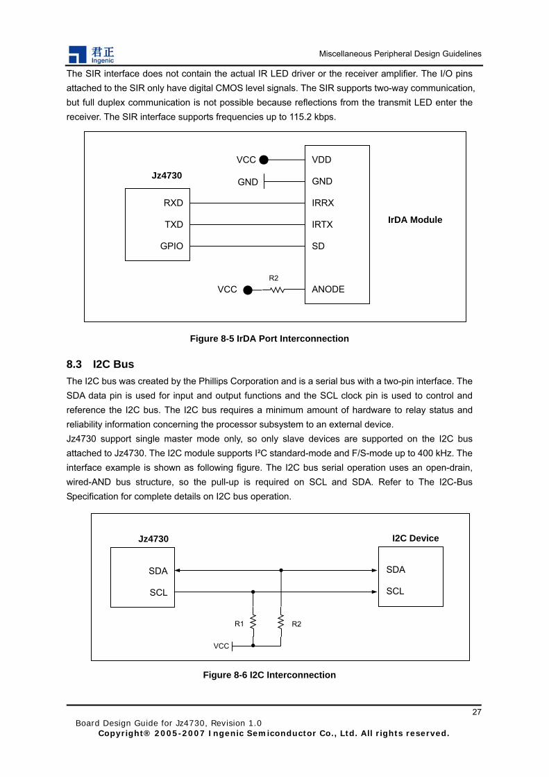
The SIR interface does not contain the actual IR LED driver or the receiver amplifier. The I/O pins attached to the SIR only have digital CMOS level signals. The SIR supports two-way communication, but full duplex communication is not possible because reflections from the transmit LED enter the receiver. The SIR interface supports frequencies up to 115.2 kbps.
Board Design Guide for Jz4730, Revision 1.0
Copyright® 2005-2007 Ingenic Semiconductor Co., Ltd. All rights reserved.
27
Figure 8-5 IrDA Port Interconnection
8.3 I2C Bus The I2C bus was created by the Phillips Corporation and is a serial bus with a two-pin interface. The SDA data pin is used for input and output functions and the SCL clock pin is used to control and reference the I2C bus. The I2C bus requires a minimum amount of hardware to relay status and reliability information concerning the processor subsystem to an external device. Jz4730 support single master mode only, so only slave devices are supported on the I2C bus attached to Jz4730. The I2C module supports I²C standard-mode and F/S-mode up to 400 kHz. The interface example is shown as following figure. The I2C bus serial operation uses an open-drain, wired-AND bus structure, so the pull-up is required on SCL and SDA. Refer to The I2C-Bus Specification for complete details on I2C bus operation.
RXD
TXD
GPIO
Jz4730 VDD
GND
IRRX
IRTX
SD
ANODE
IrDA Module
GND
VCC
R2 VCC
SDA
SCL
Jz4730
SDA
SCL
I2C Device
R2
VCC
R1
Figure 8-6 I2C Interconnection

Miscellaneous Peripheral Design Guidelines
8.4 PWM The Pulse Width Modulator (PWM) is used to control the back light inverter or adjust bright or contrast of LCD panel and also can be used to generate tone. PWM consists of a simple free-running counter with two compared registers, each compare register performs a particular task when it matches the count value. The period comparator causes the output pin to be set and the free-running counter to reset when it matches the period value. The width comparator causes the output pin to reset when the counter value matches. Jz4730 contains two pulse width modulators: PWM0 and PWM1.
8.5 GPIO The Jz4730 processor provides 120 multiplexed General Purpose I/O (GPIO) pins for use in generating and capturing application-specific input and output signals. Each pin can be programmed as an output, an input or function pin that serves certain peripheral. As input, pull up/down can be enabled/disabled for the pin and the pin also can be configured as level or edge tripped interrupt source. Note: If a GPIO is used as a wakeup source of HIBERNATE mode, it must be configured as an input in the GPIO Controller and either rising edge or falling edge must be selected in the HRER or HFER. Only GPIO16, 17, 21, 23 and GPIO96~103 can be used to wakeup HIBERNATE mode.
8.6 Smart-Card Smart Card Controller (SCC) interface is a primary device and communications interface for kinds of IC cards. The SCC interface supports communication with smart cards as specified in standard ISO7816-3. There are two SCC interfaces integrated in Jz4730. The following is a example of smart-card implementation.
VCC
CLK
RST#
IO
GND
SWB SWA
CLK_IN VCC_OUT
DATA CLK_OUT
RST_IN RST_OUT
M1 IO
M2 GND
C+
C-
SCC_CLK
SCC_DATA
GPIO
GPIO
GPIO
GPIO
Jz4730 LT1555L SOCKET
C1 R1 3.3V
C2
Figure 8-7 Smart Card implementation
Board Design Guide for Jz4730, Revision 1.0 Copyright® 2005-2007 Ingenic Semiconductor Co., Ltd. All rights reserved.
28
Miscellaneous Peripheral Design Guidelines
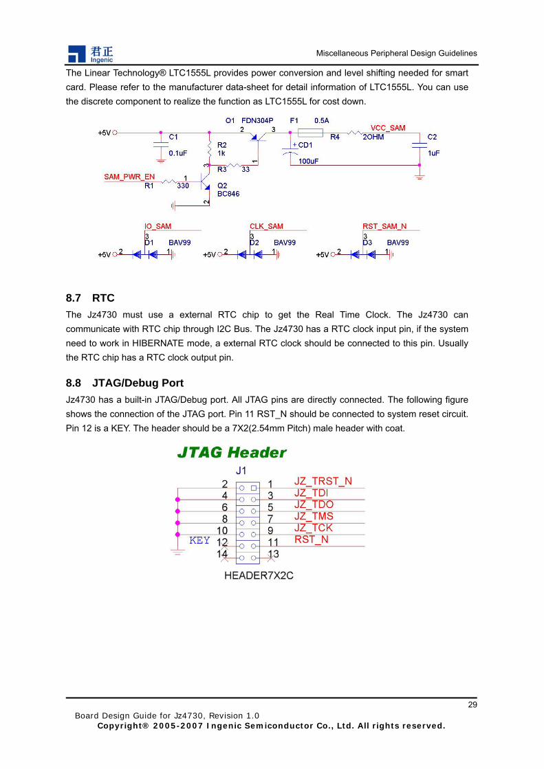
The Linear Technology® LTC1555L provides power conversion and level shifting needed for smart card. Please refer to the manufacturer data-sheet for detail information of LTC1555L. You can use the discrete component to realize the function as LTC1555L for cost down.
8.7 RTC The Jz4730 must use a external RTC chip to get the Real Time Clock. The Jz4730 can communicate with RTC chip through I2C Bus. The Jz4730 has a RTC clock input pin, if the system need to work in HIBERNATE mode, a external RTC clock should be connected to this pin. Usually the RTC chip has a RTC clock output pin.
8.8 JTAG/Debug Port Jz4730 has a built-in JTAG/Debug port. All JTAG pins are directly connected. The following figure shows the connection of the JTAG port. Pin 11 RST_N should be connected to system reset circuit. Pin 12 is a KEY. The header should be a 7X2(2.54mm Pitch) male header with coat.
Board Design Guide for Jz4730, Revision 1.0
Copyright® 2005-2007 Ingenic Semiconductor Co., Ltd. All rights reserved.
29

Platform Clock Guidelines
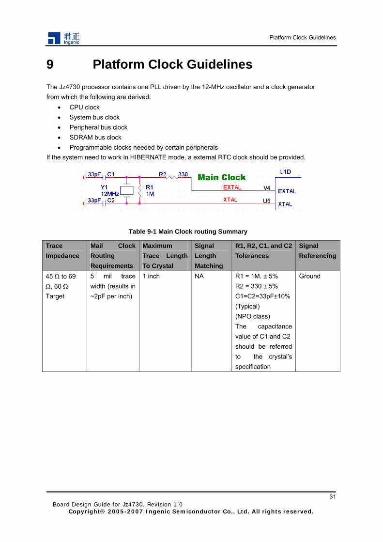
9 Platform Clock Guidelines The Jz4730 processor contains one PLL driven by the 12-MHz oscillator and a clock generator from which the following are derived:
• CPU clock • System bus clock • Peripheral bus clock • SDRAM bus clock • Programmable clocks needed by certain peripherals
If the system need to work in HIBERNATE mode, a external RTC clock should be provided.
Table 9-1 Main Clock routing Summary
Board Design Guide for Jz4730, Revision 1.0
Copyright® 2005-2007 Ingenic Semiconductor Co., Ltd. All rights reserved.
31
Trace Impedance
Mail Clock Routing Requirements
Maximum Trace Length
Signal R1, R2, C1, and C2 Signal Length Tolerances Referencing
To Crystal Matching 5 mil trace width (results in ~2pF per inch)
1 inch NA R1 = 1M. ± 5% Ground 45 Ω to 69 Ω, 60 Ω Target
R2 = 330 ± 5% C1=C2=33pF±10% (Typical) (NPO class) The capacitance value of C1 and C2 should be referred to the crystal’s specification

Platform Power Guidelines
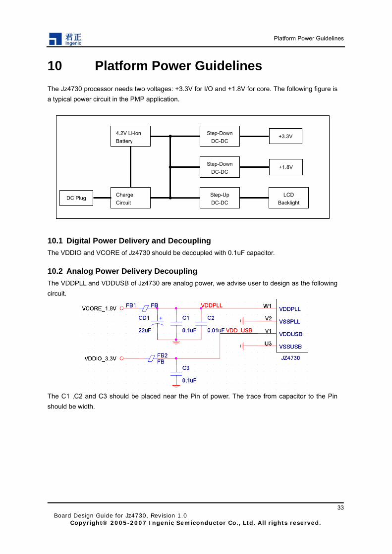
10 Platform Power Guidelines The Jz4730 processor needs two voltages: +3.3V for I/O and +1.8V for core. The following figure is a typical power circuit in the PMP application.
+3.3V Step-Down DC-DC
4.2V Li-ion Battery
+1.8V Step-Down DC-DC
Step-Up DC-DC
LCD Backlight
Charge Circuit
DC Plug
10.1 Digital Power Delivery and Decoupling The VDDIO and VCORE of Jz4730 should be decoupled with 0.1uF capacitor.
10.2 Analog Power Delivery Decoupling The VDDPLL and VDDUSB of Jz4730 are analog power, we advise user to design as the following circuit.
The C1 ,C2 and C3 should be placed near the Pin of power. The trace from capacitor to the Pin should be width.
Board Design Guide for Jz4730, Revision 1.0
Copyright® 2005-2007 Ingenic Semiconductor Co., Ltd. All rights reserved.
33