Blue Wavelength From A Diode Laser
4
ʕ 18 ʕ 160ɹɹಛɹRÜTERING and BRITTENɿBlue Wavelength From A Diode Laser ― New horizon for advanced laser processing ― ՃͷΊͷߴग़੨৭ಋମϨʔβ ಛɹɹ 1.ɹHigh power blue diode laser as enabler for copper material processing Continuous wave ʢcwʣ powered laser applications in the industrial field of welding, cladding, surface treatment, hardening, brazing, cutting and even more had been established since the late 70’s in the last century. Over time the field of applications has widened to pulsed, short pulsed and latest ultra- short pulsed lasers. Laser based applications can be rated next to cw or pulsed by the power applied and the wavelength used. The latter is related to the laser active material the laser is using to create the laser radiation. Well known materials to create a laser beam, powerful enough for industrial applications are i. Nd:YAG lasers using a solid state crystal from yittrium- aluminium-garnet, doped with Nd 3+ Ions. Next to YAG, there is other crystal which can be doped with the Nd 3+ Ions. ii. CO 2 -lasers using a gas mixture from helium, nitrogen and carbon-dioxide. iii. Yb:glass fiber lasers using quite thin glass fibers which are doped with Yb xx ions. iv. Yb:YAG disc lasers using a yittrium-aluminium-garnet doped with Yb xx ions. v. Semiconductor ʢor diodeʣ lasers using basically material in the GaAs field, sometime doped with additional ingredients. vi. Excimer lasers using a gas mixture of a halogen and an inert gas. The above named lasers are standing for the most common technologies in CW lasers and of course are not covering all available or used possibilities. All laser active materials must be supplied with energy to create the laser beam. This is called pumping. The energy source can be light ʢ1/3/4ʣ , can be a gas discharge ʢ2/6ʣ or electrical current ʢ5ʣ . From Fig. 1 it can be seen that the shortest wavelength in the UV regime is offered by the Excimer lasers, followed by several lasers in the area of around 1 μm in the near infrared and finally the CO 2 -laser in the far infrared. The latest developments of semiconductor materials allowed lasers based on GaN rather than GaAs. The outcome is a radiation with 450 nm in the visible and blue part of the spectrum. Fig. 1 shows the wavelength of the named laser active materials. Some of these lasers can be designed and build in a way to double or even triple their wavelengths, especially Nd:YAG-, Yb:YAG- and Yb:glass lasers are known for this. This is for example getting us to wavelengths like 515 and 532 nm which is in the visible green area of the electromagnetic spectrum. However, these laser sources are working based on a conversion process, in which a crystal is converting only a fraction of the pumped laser wavelength into the target wavelength. The conversion process leads to high power losses, complex cooling requirements and a sophisticated optical set-up. Nd:YAG lasers are mainly pulsed and don’t play any role in CW applications today. In marking, scribing, micro applications and pulsed cutting they are widely used but will not be further reviewed in this article. Same for Excimer lasers which play e.g. a big role in processing of OLED displays. As CO 2 -lasers with their far infrared wavelength have a very different approach to applications we as well rule them out for further review. This leaves us with lasers around 1μm, their frequency doubled spin- offs and the new developed diode lasers with blue radiation. Blue Wavelength From A Diode Laser ʕ New Horizon for Advanced Laser Processing ʕ RÜTERING Markus and BRITTEN Simon Laserline GmbHʢFraunhofer Straße, 56218 Mülheim-Kärlich, Germanyʣ ʢReceived June 25, 2018ʣ Key wordsɿ blue wavelength, 450 nm, diode laser, laser welding, laser cladding, copper, power electronics, battery joining, reliable welding, Laserline YAG frequency doubled CO2 VIS UV NIR Mid-IR FIR 400nm 700nm 3μm 30μm Excimer 100nm XRay Yb:YAG Nd:YAG Yb:Glas 1μm InGaAs Fig. 1 Main lasers in Materials Processing wavelengths [Source Wikipedia.org].
Transcript of Blue Wavelength From A Diode Laser

― 18―
160 特集 RÜTERING and BRITTEN:Blue Wavelength From A Diode Laser ―New horizon for advanced laser processing―
次世代加工のための高出力青色半導体レーザ特 集
1. High power blue diode laser as enabler for copper material processing
Continuous wave(cw)powered laser applications in the industrial field of welding, cladding, surface treatment, hardening, brazing, cutting and even more had been established since the late 70’s in the last century. Over time the field of applications has widened to pulsed, short pulsed and latest ultra-short pulsed lasers. Laser based applications can be rated next to cw or pulsed by the power applied and the wavelength used. The latter is related to the laser active material the laser is using to create the laser radiation. Well known materials to create a laser beam, powerful enough for industrial applications are
i. Nd:YAG lasers using a solid state crystal from yittrium-aluminium-garnet, doped with Nd3+ Ions. Next to YAG, there is other crystal which can be doped with the Nd3+ Ions.
ii. CO2-lasers using a gas mixture from helium, nitrogen and carbon-dioxide.
iii. Yb:glass fiber lasers using quite thin glass fibers which are doped with Ybxx ions.
iv. Yb:YAG disc lasers using a yittrium-aluminium-garnet doped with Ybxx ions.
v. Semiconductor(or diode)lasers using basically material in the GaAs field, sometime doped with additional ingredients.
vi. Excimer lasers using a gas mixture of a halogen and an inert gas.
The above named lasers are standing for the most common technologies in CW lasers and of course are not covering all available or used possibilities. All laser active materials must be supplied with energy to create the laser beam. This is called pumping. The energy source can be light(1/3/4), can be a gas discharge(2/6)or electrical current(5).
From Fig. 1 it can be seen that the shortest wavelength in the UV regime is offered by the Excimer lasers, followed by several lasers in the area of around 1 μm in the near infrared and finally
the CO2-laser in the far infrared. The latest developments of semiconductor materials allowed lasers based on GaN rather than GaAs. The outcome is a radiation with 450 nm in the visible and blue part of the spectrum.
Fig. 1 shows the wavelength of the named laser active materials.
Some of these lasers can be designed and build in a way to double or even triple their wavelengths, especially Nd:YAG-, Yb:YAG- and Yb:glass lasers are known for this. This is for example getting us to wavelengths like 515 and 532 nm which is in the visible green area of the electromagnetic spectrum. However, these laser sources are working based on a conversion process, in which a crystal is converting only a fraction of the pumped laser wavelength into the target wavelength. The conversion process leads to high power losses, complex cooling requirements and a sophisticated optical set-up.
Nd:YAG lasers are mainly pulsed and don’t play any role in CW applications today. In marking, scribing, micro applications and pulsed cutting they are widely used but will not be further reviewed in this article. Same for Excimer lasers which play e.g. a big role in processing of OLED displays. As CO2-lasers with their far infrared wavelength have a very different approach to applications we as well rule them out for further review. This leaves us with lasers around 1μm, their frequency doubled spin-offs and the new developed diode lasers with blue radiation.
Blue Wavelength From A Diode Laser―New Horizon for Advanced Laser Processing―
RÜTERING Markus and BRITTEN Simon
Laserline GmbH(Fraunhofer Straße, 56218 Mülheim-Kärlich, Germany)
(Received June 25, 2018)
Key words: blue wavelength, 450 nm, diode laser, laser welding, laser cladding, copper, power electronics, battery joining,reliable welding, Laserline
YAGfrequency doubled
CO2
VISUV NIR Mid-IR FIR400nm 700nm 3μm 30μm
Excimer
100nmXRay
Yb:YAGNd:YAGYb:Glas
1μm
InGaAs
Fig. 1 Main lasers in Materials Processing wavelengths [Source Wikipedia.org].

― 19―
レーザ加工学会誌 Vol. 25, No. 3 (2018) 161
2. Blue Laser Diode Motivation
The motivation to develop lasers with a wavelength in the blue regime is based on the absorption of laser radiation in specific materials. Fig. 2 shows the reflectance as complement to absorption at room temperature for certain materials in relation to the wavelength. It can easily be seen that copper and gold show a huge advantage for the blue wavelength. Processing these materials with near infrared wavelength is possible but requires a high average power and has further disadvantages as soon as the copper melts. Absorption and heat conductivity change substantially when melting copper making the process instable and often not fit for 24/7 production lines. To overcome this problem green wavelength had been investigated1), the results had been better than IR lasers, but still there had been issues left with thin materials as one example. In addition the conversion efficiency is less than 50% which drives the necessary invest and the cost of ownership is increased as well.
There is a slight decrease in reflectance for steel materials as well as aluminum for green and blue, but this moderate advantage is not paying off towards the invest cost. Summarizing the intention for the blue diode laser is processing copper and gold in the first step, whereas not all possible ideas have been reviewed yet.
Laserline, who established high power diode lasers more than 20 years ago, and is the market leader for such lasers has teamed up with OSRAM, Max-Born-Institute and Coherent | DILAS in a public funded project3). The actual ongoing project has set the goal to develop a blue diode laser with 1000 W of CW power. The recent results achieved over 700 W(Fig. 3)and were applied in some applications already
During the 2018 AKL conference in Aachen,(Germany, www.lasercongress.org)5) Laserline presented a comparison for copper and gold processing, in which the overall efficiency between infrared lasers and blue laser was discussed. The result showed a total energy saving in copper processing of 84% and for gold
it even summed to a saving of 92%, if the higher absorption for each material is used to reduce the necessary power from 10 kW to 1 kW respectively 500 W to achieve the same results. Next to the absorption we need to take into account, that the heat conduction is about 390 W/mK for copper compared to 15 W/mK for stainless steel. So overall it is not only difficult to place the energy into the specimen but also much harder to “use” it in the application rather than losing it into the material.
3. Blue Laser Diode Technology
The company OSRAM designed laser bars using GaN(Gallium Nitride)to create the wavelength of 450 nm. Laserline used its unique technology to mount, electrically connect and cool the blue laser bars on heat sinks. Each diode bar is actually creating a power level of up to 50 Watts. Using special optics it is possible to combine several mounted diode bars in a stack and even combine 2 stacks in one laser source(Fig. 4).
The standard fiber optic system can be used to carry the blue laser radiation to the workpiece and offer all the flexibility which is known from the standard diode lasers. In this actual case the fiber optic is a 600 μm fiber and the output is realized with a beam quality of approx. 60 mm mrad. The processing heads which are well known in the industry can be used as well for welding, cladding and soldering only the anti-reflective coating needs to be adapted for 450 nm. Otherwise there would be losses
Blue DiodeYb:YAG SHG
Yb:YAGCO2
100
80
60
40
20
00.2 1.0 10.0
Ref
lect
ance
[%] Cu
Au
Wavelength [μm]
Fig. 2 Main lasers wavelengths in materials processing2).
Table 1 Comparison of IR and blue radiation for processing high reflective materials.
Fig. 3 Laser performance curve of the 700W blue diode laser system4).

― 20―
162 特集 RÜTERING and BRITTEN:Blue Wavelength From A Diode Laser ―New horizon for advanced laser processing―
in power on every optical surface. So almost all of the basic tools in material processing are at hand already in this starting phase. Future development will as well cover scanning technologies and various hybrid technologies in applications.
4. Blue Laser Diode Applications
The resulting laser power of over 700 W with a wavelength of 450nm enables a reproducible processing of pure copper material with a precise energy deposition in the full power range. For conventional IR laser systems a stable process regime without the application of a deep penetration keyhole welding is not possible due to the low absorption and the high heat conductivity of copper. In direct comparison between the IR and the blue system, the IR depicts instable welding conditions resulting in a missing weld or a highly varying welding depth(Fig. 5 left). With the application of the wavelength of 450 nm, a melting of copper material in the heat conduction mode is possible for the first time, allowing the precise adjustment of the melt pool geometry also for thin copper materials(Fig. 5 right). The part in this picture is a bead on plate weld of a 0.3 mm thick copper foil. The welding speed was chosen at 2 m/min for this heat conduction welding, but could be varied with still good results.
A stable energy deposition and heat conduction process regime is especially important for applications, where the high pressure of a keyhole welding mode would lead to a cutting of the material or an undesirable spatter occurrence. This is can occur while welding stacked thin copper foils, which may be subject to an uncontrolled gap due to warping of the stacked foils.
While applying a butt welding approach with 580 W laser power and 2 m/min feeding speed on stacked copper foils, a weld bead width of more than 0.8 mm can be created with minimal porosity and low undercut(Fig. 6 left). For a fillet weld approach with an irradiation on the edge of the foil stack, the foil endings are molten into a high cross –section area with a complete attachment to the solid foils(Fig. 6 right). In both butt and edge welding the process results in a perfect mechanical joint as well as in a very good electrical conductivity.
Another perspective is the welding of dissimilar metals such as copper and aluminum. Due to the different melting temperatures of the materials and the low absorption of IR in
copper, an insufficient melting of the coppers occurs. This results in a joint which is similar to brazing instead of a high strength joint. With a high absorption of blue in the copper material, the melting of the copper can be controlled and both materials can be welded in butt weld configuration.
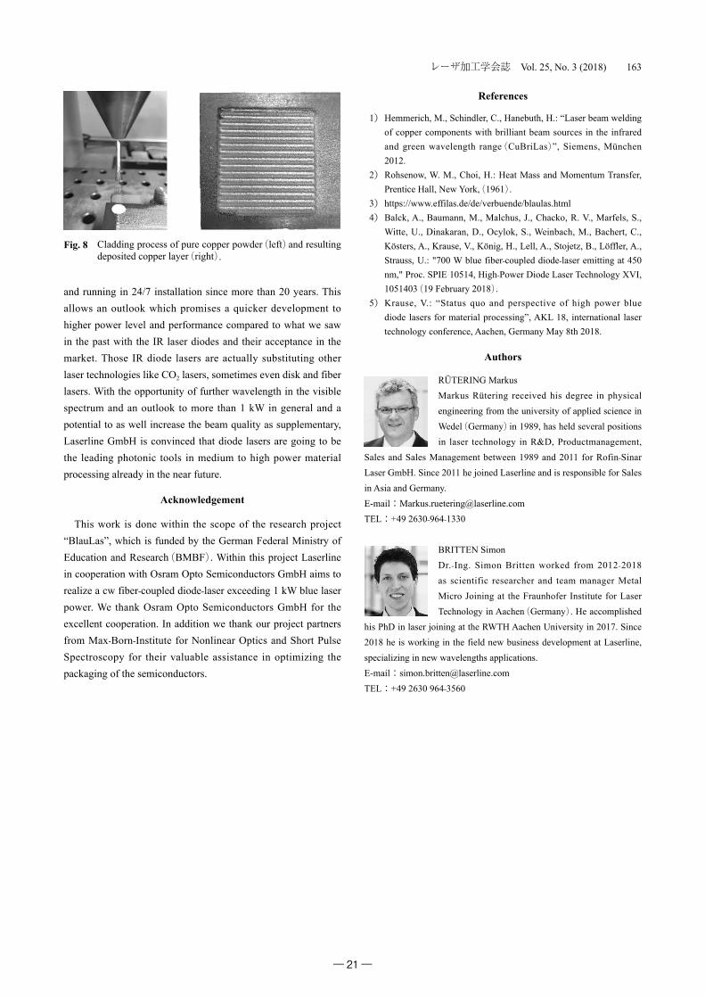
Finally the additive manufacturing of pure copper powder onto copper or other basic material requires a highly reproducible melting of the powder material. A blue cladding process can be applied for the selective coating of steel, nickel and aluminum base materials or for the cladding of complex shaped parts as in the printing of 3D components. First results as shown in Fig. 8 are very positive, more investigation is necessary to improve the powder efficiency and overall performance.
5. Conclusion
Having shown the motivation, technology and some results of a blue diode laser with cw high power output, it is obvious to push this technology into the market in the near future. The basic technology of cooling and electrically connecting and beam forming the blue diode bars is available since long, well matured
Fig. 4 Power scaling technology in the Laserline Blue Diode Laser.
Fig. 5 Comparison of welding results with IR and Blue laser on copper foil.
Fig. 6 Welding of 34 stacked copper foils(each 11μm)in butt welding(left)and edge welding configuration(right).
Fig. 7 Joint between an aluminum(0.8 mm)and copper sheet(0.4 mm)in butt weld configuration(Laser power 500 W, feeding velocity 1.5 m/min, focus ϕ0.6 mm).
― 21―
レーザ加工学会誌 Vol. 25, No. 3 (2018) 163
and running in 24/7 installation since more than 20 years. This allows an outlook which promises a quicker development to higher power level and performance compared to what we saw in the past with the IR laser diodes and their acceptance in the market. Those IR diode lasers are actually substituting other laser technologies like CO2 lasers, sometimes even disk and fiber lasers. With the opportunity of further wavelength in the visible spectrum and an outlook to more than 1 kW in general and a potential to as well increase the beam quality as supplementary, Laserline GmbH is convinced that diode lasers are going to be the leading photonic tools in medium to high power material processing already in the near future.
Acknowledgement
This work is done within the scope of the research project “BlauLas”, which is funded by the German Federal Ministry of Education and Research(BMBF). Within this project Laserline in cooperation with Osram Opto Semiconductors GmbH aims to realize a cw fiber-coupled diode-laser exceeding 1 kW blue laser power. We thank Osram Opto Semiconductors GmbH for the excellent cooperation. In addition we thank our project partners from Max-Born-Institute for Nonlinear Optics and Short Pulse Spectroscopy for their valuable assistance in optimizing the packaging of the semiconductors.
References
1) Hemmerich, M., Schindler, C., Hanebuth, H.: “Laser beam welding of copper components with brilliant beam sources in the infrared and green wavelength range(CuBriLas)”, Siemens, München 2012.
2) Rohsenow, W. M., Choi, H.: Heat Mass and Momentum Transfer, Prentice Hall, New York,(1961).
3) https://www.effilas.de/de/verbuende/blaulas.html4) Balck, A., Baumann, M., Malchus, J., Chacko, R. V., Marfels, S.,
Witte, U., Dinakaran, D., Ocylok, S., Weinbach, M., Bachert, C., Kösters, A., Krause, V., König, H., Lell, A., Stojetz, B., Löffler, A., Strauss, U.: "700 W blue fiber-coupled diode-laser emitting at 450 nm," Proc. SPIE 10514, High-Power Diode Laser Technology XVI, 1051403(19 February 2018).
5) Krause, V.: “Status quo and perspective of high power blue diode lasers for material processing”, AKL 18, international laser technology conference, Aachen, Germany May 8th 2018.
Authors
RÜTERING Markus Markus Rütering received his degree in physical engineering from the university of applied science in Wedel(Germany)in 1989, has held several positions in laser technology in R&D, Productmanagement,
Sales and Sales Management between 1989 and 2011 for Rofin-Sinar Laser GmbH. Since 2011 he joined Laserline and is responsible for Sales in Asia and Germany.E-mail:[email protected]:+49 2630-964-1330
BRITTEN SimonDr.-Ing. Simon Britten worked from 2012-2018 as scientific researcher and team manager Metal Micro Joining at the Fraunhofer Institute for Laser Technology in Aachen(Germany). He accomplished
his PhD in laser joining at the RWTH Aachen University in 2017. Since 2018 he is working in the field new business development at Laserline, specializing in new wavelengths applications.E-mail:[email protected]:+49 2630 964-3560
Fig. 8 Cladding process of pure copper powder(left)and resulting deposited copper layer(right).