
Bit-Serial Parallel Processing Systems - Kent State … · Bit-Serial Parallel Processing Systems ....
8
377 II:EE TR!\NS!\CTI01'.S or-: COMPL.;lERS. 1i 0L e-31 . ,"0. S. MAY 19 8 2 Bit-Serial Parallel Processing Systems KENNETH E. BATCHER Abstract-About a decade ago, a bit-serial parallel processing system STARAN® 1 was developed. It used standard integrated circuits that were available at that time. Now, with the availability of VLSI, a much greater processing capability can be packed in a unit volume. This has Jed to the recent development of two bit-serial parallel pro- cessing systems: an airborne associative processor and a ground based massively parallel processor. The airborne associative processor has about the same processing capability as a three cabinet STARA N system in a volume less than 0.5 cubic feet. The power required and weight ' are also reduced dra- matically for the airborne environment. The massively parallel processor has about 100 times tbe processing capability as STA RAN system in about the same volume. Floating point speeds are better than 100 MOPS (million operations per second). Integer arithmetic speeds depend on operand lengths-for 16 bit in- tegers the speed is better than 3000 MOPS for addition and 450 MOPS for multiplication. After presenting the basic rationale for bit-serial parallel processors, the organizations of the two recent systems are shown and some of their applications are outlined. . Index Terms-Airborne processors, bit-serial processors, custom VI.SI chips, image processing, multidimensional access, parallel processors, radar processing. I. INTRODUCTION L IKE other parallel processing systems, the systems we describe in this paper have a number of processing ele- ments (PE's) operating in parallel on separate data streams under the control of a single control unit. The systems have a large number of processing elements (in the thousands) and each element is very simple-operating on its data stream bit by bit. Thus, we call them bit-serial parallel processing systems. Given an array of 1000 16 bit items , a conventional computer would process the array item by item in 1000 steps, whereas a bit-serial parallel processor would process the array broadside in 16 steps with each processing element treating a bit of one item on each step . The array is acces' sed by bit-slices instead of by items. Since the number of items in a typical array is much larger than the number of bits per item, processing is much faster. A feature of bit-serial processing is its ability to handle data items of any length . There is no need to extend operands with filler bits to pack them into standard machine words as in a conventional computer. This raises the storage and processing Manuscript received June 4. 19!iL revised December 10 . 19K!. The author is with the Di!t ital Technology Department. Goodyear Acro- space Corporation. Akron. OH 443 IS. Registered Trademark, Goodyear Aerospace Corporation. Akron. OH 44315. efficiency. Suppose we have an array of M operands with N bits per operand. Any parallel processor suffers some loss in efficiency when M is less than the num ber of processing ele- ments . A conventional computer experiences a similar loss in efficiency when N is less than its word length . Parallel pro- cessors with processing elements of a standard word length suffer from both losses in efficiency when M is less than the number of PE's, and when N is less than the word length of a PE. Bit-serial parallel processors, like conventional computers, experience only one inefficiency. Another advantage of bit-serial parallel processors occurs when only a part of the operand needs treatment. For example, only one cycle is required to test the signs of all elements in an array. Associative processing where data items are addressed by content is easily performed by reading out the keys bit by bit and comparing their values to the bits of a comparand . Only the keys involved in the search need be accessed. While a data array would be accessed broadside by the set of processing elements, the same array would be read and written in the orthogonal direction (item by item) by input- output channels. This is the normal way data arrays are gen- erated, stored, output, and processed in conventional com- puters . We should accommodate the rest of the world rather than force it to transfer data arrays by bit-slices. Thus, we need a means of accessing data in two directions: item by item for input and output and bit-slice by bit-slice for the set of pro- cessing elements . In ST ARAN® processors, data arrays are stored in multi- dimensional access memories [1]. [2] so they can be accessed in either direction equally well. The memories use the same kind of random access memory integrated circuits as con- ventional solid-state stores. The locations of the data bits are scrambled a certain way so data arrays can be accessed many different ways including the orthogonal directions . The in- clusion of a few EXCLUSIVE-OR gates in the memory address bus genera tes the necessary addresses for the memory ele- ments. A network called the flip network [3] is included in the memory data bus to scramble data being written into storage. and to unscramble data being read from storage. This network is also used to route data between processing elements and is akin to a number of multistage interconnection networks [4]. The first ST ARAN was demonstrated in 1972. It used standard off-the-shelf integrated circuits that were available at that time . Now with the availability of VLSl , much greater packing densities can be obtained. This has led to the recent development of two bit-serial parallel processors: the airborne associative processor and the massively parallel processor. 0018-9340/82/0500-0377$00.75 © 1982 IEEE I
-
Upload
truongtruc -
Category
Documents
-
view
229 -
download
0
Transcript of Bit-Serial Parallel Processing Systems - Kent State … · Bit-Serial Parallel Processing Systems ....

377 IIEE TRNSCTI01S or- COMPLlERS 1i0L e-31 0 S MAY 19 8 2
Bit-Serial Parallel Processing Systems
KENNETH E BATCHER
Abstract-About a decade ago a bit-serial parallel processing system STARANreg 1 was developed It used standard integrated circuits that were available at that time Now with the availability of VLSI a much greater processing capability can be packed in a unit volume This has Jed to the recent development of two bit-serial parallel proshycessing systems an airborne associative processor and a ground based massively parallel processor
The airborne associative processor has about the same processing capability as a three cabinet STARA N system in a volume less than 05 cubic feet The power required and weight are also reduced drashymatically for the airborne environment
The massively parallel processor has about 100 times tbe processing capability as tb~ STA RAN system in about the same volume Floating point speeds are better than 100 MOPS (million operations per second) Integer arithmetic speeds depend on operand lengths-for 16 bit inshytegers the speed is better than 3000 MOPS for addition and 450 MOPS for multiplication
After presenting the basic rationale for bit-serial parallel processors the organizations of the two recent systems are shown and some of their applications are outlined
Index Terms-Airborne processors bit-serial processors custom VISI chips image processing multidimensional access parallel processors radar processing
I INTRODUCTION
L IKE other parallel processing systems the systems we describe in this paper have a number of processing eleshy
ments (PEs) operating in parallel on separate data streams under the control of a single control unit The systems have a large number of processing elements (in the thousands) and each element is very simple-operating on its data stream bit by bit Thus we call them bit-serial parallel processing systems Given an array of 1000 16 bit items a conventional computer would process the array item by item in 1000 steps whereas a bit-serial parallel processor would process the array broadside in 16 steps with each processing element treating a bit of one item on each step The array is accessed by bit-slices instead of by items Since the number of items in a typical array is much larger than the number of bits per item processing is much faster
A feature of bit-serial processing is its ability to handle data items of any length There is no need to extend operands with filler bits to pack them into standard machine words as in a conventional computer This raises the storage and processing
Manuscript received June 4 19iL revised December 10 19K The author is with the Dit ital Technology Department Goodyear Acroshy
space Corporation Akron OH 443 IS Registered Trademark Goodyear Aerospace Corporation Akron OH
44315
efficiency Suppose we have an array of M operands with N bits per operand Any parallel processor suffers some loss in efficiency when M is less than the num ber of processing eleshyments A conventional computer experiences a similar loss in efficiency when N is less than its word length Parallel proshycessors with processing elements of a standard word length suffer from both losses in efficiency when M is less than the number of PEs and when N is less than the word length of a PE Bit-serial parallel processors like conventional computers experience only one inefficiency
Another advantage of bit-serial parallel processors occurs when only a part of the operand needs treatment For example only one cycle is required to test the signs of all elements in an array Associative processing where data items are addressed by content is easily performed by reading out the keys bit by bit and comparing their values to the bits of a comparand Only the keys involved in the search need be accessed
While a data array would be accessed broadside by the set of processing elements the same array would be read and written in the orthogonal direction (item by item) by inputshyoutput channels This is the normal way data arrays are genshyerated stored output and processed in conventional comshyputers We should accommodate the rest of the world rather than force it to transfer data arrays by bit-slices Thus we need a means of accessing data in two directions item by item for input and output and bit-slice by bit-slice for the set of proshycessing elements
In STARANreg processors data arrays are stored in multishydimensional access memories [1] [2] so they can be accessed in either direction equally well The memories use the same kind of random access memory integrated circuits as conshyventional solid-state stores The locations of the data bits are scrambled a certain way so data arrays can be accessed many different ways including the orthogonal directions The inshyclusion of a few EXCLUSIVE-OR gates in the memory address bus genera tes the necessary addresses for the memory eleshyments A network called the flip network [3] is included in the memory data bus to scramble data being written into storage and to unscramble data being read from storage This network is also used to route data between processing elements and is akin to a number of multistage interconnection networks [ 4]
The first STARAN was demonstrated in 1972 It used standard off-the-shelf integrated circuits that were available at that time Now with the availability of VLSl much greater packing densities can be obtained This has led to the recent development of two bit-serial parallel processors the airborne associative processor and the massively parallel processor
0018-9340820500-0377$0075 copy 1982 IEEE
I
---378
II AIRBORNE ASSOCIATIVE PROCESSOR
During 1978 studies to determine the feasibility of an airshyborne version of a ST ARAN processor were conducted under company reseach and development programs and under US Navy contracts The studies culminated in the design of an airborne associative processor using VLSI [5] The architecshyture of the processor is shown in Fig I The five major blocks are as follows
I) the array unit containing over 2000 PEs and over I Mbyte of data storage
2) the array control unit which supplies the control signals for the array unit
3) the register and arithmetic section which controls the input and output of array unit data and generates array adshydresses
4) the program execution control unit which executes the application program and drives the array control unit and the register and arithmetic section and
5) the control memory which stores the application proshygram and buffers data between the airborne associative proshycessor and a host computer
A Array Unit
The array unit comprises 17 array modules 16 for the apshyplication and a spare module to replace any other array module found to be in error Each array module contains 128 PEs and four 32 X 4096 bit arrays of multidimensional access storage Thus the array unit contains 2048 PEs (plus spare) and one Mbyte of data storage (plus spare)
Fig 2 depicts one array module The module contains four custom design VLSI chips with each chip containing the regshyisters for 32 PEs a 32 line nip network and a resolver (Fig 3) The multidimensional access memories for one array module are packaged in eight hybrid packages with each hyshybrid containing 16 1 K X 4 random access memory (RAM) chips The 32 PEs of one VLS[ chip access the storage of two memory hybrid circuits through the 32 line nip network on the VLSI chip The arrangement is akin to one STARAN array module except that the nip network is only 32 lines wide inshystead of 256 lines wide [I] [3] The multidimensional access memories allow the register and arithmetic section to input or output all bits of a 32 bit operand in one memory cycle and the set of PEs to access one bit-slice from all operands in one memory cycle
The processing elements are much like the PEs of STARshyAN Each PE contains a one bit X-register and a one bit Yshyregister which perform the bulk of the bit-serial arithmetic [6] The one-bit mask register holds a mask bit which governs writing of PE data into the multidimensional access storage in masked-write operations Each PE also has a one bit hold register for masked-write operations This register was not needcd in ST ARAN systems because they performed masked writes by selectively setting the write-enable pins of the memory chips In the airborne associative processor the memory chips are four bit wide so individual masking is not possible at the memory chips Masked write operations are performed by rcading the memory data into the hold register
IEEE TRANSACTIONS ON COMPUTERS VOL C-]I NO 5 MAY 1982
+
DATA MEMORY BUS A
CO~T ROL DATAI--- shyMEMORY MEMORY
BU S B
OAT A III STR t t
ARRAY CONT ROL
INS T R PROGRAM EXECUTIO~
CONT ROL
CONTROL REG amp
AR ITH
DATA amp t CO~HROL ADDRESSES
~RRAY UNIT
Fig I BlOCK diagram of the airborne associative processor
I~EMJRY
HI BR I 0
VL S I I-- shyr-- shy CH I P
ME MD R Y
MY BR IJ
I I
r~E~ORY
HYBRID I-- shyVL S I
CHIP I-- shyEMORY
HYBRID
f- shyCOMMON
J 0
ME~ORY
HYBRID -VL S I
CHIP I-- shyHE MO R Y
HY BR 10
I [
MEMORY
HY SR I 0 I-- shyVL S I
CHI P r-- shyMEMORY
HY8RJo
Fig 2 One airborne associative processor array module
ARRAY ADORE SS
TOI FRO COMMON REG 15 TE A
Fig 3 Custom PEjnip network chip
IIE~ORY Bi))
changing those data bits where the mask register is set and then writing the data back into the multidimensional access memory
The resolver on each PEl Flip network chip tests the 32 bit data bus for the presence of one or more I-states The SUM-OR
output is an INCLUSIVE-OR of the 32 data lines The position of a I-state is output on a 5 bit wide resolver address bus The resolver is used after associative searches After each PE has checked its associated storage for the presence or absence of data satisfying the search criteria the match bits are fed to the resolver which locates the position of onc Item matching the
379
criteri a Thc resolver outputs of the PE chips are collected together in a 5uper rC50lver to see if any of the 2048 PEs in the system have matching data and to generate the address of one match
The PE Flip network chip is a custom VlSI chip using CMOSSOS technol ogy Cycle times are longer than the STARA] cycle times which used ECl technology The set of 2048 PEs in the airborne associative processor has about the same processing power as the set of 1024 PEs in a fourshyarray STARAN system
B Array Control Unit
The array control unit broadcasts control signals to all PEs in the array unit Several basic array operations are possible using the PE registers multidimensional ac(ess storage or the common rcgister in the control unit as operands
1) the X andor Y registers can be loaded or logically combined with data from the common register the multidi shymensiona I access storage or the PE registers
2) the mask register can be loaded from the common regshyister the multidimensional access storage or the PE regisshyters
3) the multidimensional access storage can be written (eishyther masked or unmasked) with data from the common register or the PE registers and
4) the common register ca n be loaded with data from the PE registers or the multidimensional access storage
C Register and Arithmetic Section
The register and arithmetic section generates the addresses for the array unit operations and controls the input and output of array unit data It contains 24 16 bit registers two 32 bit registers an Arithmetic and Logic Unit (ALU) and a number of selection gates (Fig 4)
D Program Execution Control
The program execution control unit executes the application program Conditional branching is provided to any instruction in the control memory Instruction fetching is overlapped with execution for faster processing Besides the program counter and the instruction register the program control unit contains a stack to store up to 16 return addresses and logic to allow prioritized interrupts
E Control Memory
The control memory has three types of storage program memory holding the application program buffer memory to buffer data to and from the host computer and a read-only memory to store routines for certain essential operations such as the data transfer program and the basic built-in test roushytines The host computer is a dual processor and the buffer memory communicates with each host processor over its memory bus It has two banks each holding 819232 bit words To the host computer the buffer memory appears as one of its own memory banks (the whole airborne associative processor occupies a memory bank space in the host computer)
10 CO TR0 L ~CMORY
I I e+lt TO ARRAY I I CONTROL
I I
lftmiddot_middotshy
T O ARRPY PROCESSOR
Fig 4 Register and arit hmeti c section
F Applications
The airborne associative processor was designed to upgrade early warning radar surveillance and command and control processing aboard the Navys E-2C aircraft The E-2C is a carrier-based aircraft that receives target data from its own radar and track data from data links Targets are processed and correlated to form track data which are output to three operator displays The airborne associative processor fits inside the existing computer as an easily replaceable unit The high-speed content addressability of the airborne associative processor is used to correlate radar reports with each other and with existing tracks The software required to maintain the surveillance database is simplified as well
With suitable modifications the airborne associative proshycessor could be adapted to other uses in airborne environments or to other applications where a large amount of specialized processing power must be packed into a small volu~e
Ill MASSIVELY PARALLEL PROCESSOR
Jn 1971 the NASA Goddard Space Flight Center initia ted a program to develop high-speed image processing systems They will be required to process the large amount of image data that will come from satellites that NASA will orbit during the 1980s These systems use thousa nds of PEs operating simultaneously to achieve their speed (massive parallelism) A typical satellite image contains millions of picture elements (pixels) that can generally be processed in parallel In 1979 a contract was awarded to construct a massively parallel proshycessor to be delivered in 1982 [7] The processor has 16 896 PEs arranged in a 128 row X 132 column rectangular array The PEs are in the array unit (Fig 5) Other major blocks in the massively parallel processor are the array control unit the staging memory the program and data management unit and the interface to a host computer
A Array Unit Logically the array unit contains 16 384 PEs arranged in
a 128 row X 128 column square array Physically the array unit contains an extra 128 row X 4 column rectangle of PEs
JxO
t
PR OGRAM I OATA MAHAGEI~[NT UNIT
( POU )
Fig 5 Block diagram of the massively para ll el processor
for redundancy Each PE communicates with its four nearest neighbors north south east and west Each PE is a bit-serial processor With a 10 MHz clock rate and 16384 PEs opershyating in parallel the system has a very high processing rate Each PE can read two 16 bit integers generate their sum and store the 17 bit sum in 49 clock cycles so that 16 384 additions are performed in less than 5 JLS (more than 3000 MOPS) Floating-point operations are performed at a fast rate even though they are not particularly suited for bit-serial processing Many different noating-point formats are possible With a 32 bit format (I bit sign 7 bit base-J6 exponent and 24 bit fraction) the floating-point addition is better than 400 MOPS and multiplication is better than 200 MOPS
I) Array Topology The major application of the massively parallel processor is image processing Since most of the proshycessing is conducted between neighboring pixels it is natural to connect the thousands of PEs together in a square array with each PE communicating with its nearest neighbors We investigated the use of other interconnection networks like the multistage SIMD interconnection networks [4] but with over 16000 PEs they become unwieldy The layout of a square array is very simple with no long runs to slow down the transfer
rate Certain image processing operations like the fast Fourier
transform (FIT) require communication between pixels or points located far apart in the image If we store one point in each PE then the routing time would be severe in a nearest neighbor square array topology But this is not the best way to do FFTs on the MPP Each PE can store several points in its RAM so that the number of PEs required to do an FIT can be reduced to a small compact subarray of the array unit The processing power of the other PEs is not wasted since if we want to do one FIT we will invariably want to do many FITs so lhat we can divide the array unit up into many compact subarrays each doing one FFT For example suppose we want to do many 5120 point FITs Ten points can be packed into each PE so each FFT can be performed in a 16 row X 32 colshyumn subarray of the array unit Thirty-two such subarrays can do 32 FFTs in parallel The longest communication path in eac h FFT is half the width of the subarray (J 6 columns) so the routing time can be reduced to a fraction of the computashytion ti me
IEEE TRANSACTIONS ON COMPUTERS VOL cmiddot31 NO 5 MAY 1982
One may ask the question of how the data clln be input and output effectively especially when they have a peculiar layout like in the FIT example A 5120 point FIT is most easily performed by combining 1024 five point FITs with five 1024 point FITs where the position of any point is a function of its index modulo 5 and 1024 The 5120 points of one FIT have a scrambled layout The permutations required are akin to the permutations required to change a data array from an item by item fonnat to a bit-slice fonnat Some kind of buffer memory will be required in the array unit input-output path to convert data arrays to and from the bit-slice format If it is properly designed the same buffer memory could perform other pershymuta tions as well such as those required by the 5120 point FIT example
Thus in the massively parallel processor we use a simple square array topology in the array unit and insert a buffer memory (the staging memory) in its input-output path to perform the permutations required by particular application programs The staging memory transforms the bit-serial forshymat of the array unit to the item by item format of the outside world With 16000 PEs this is a better solution to the problem than the solution used in STARAN where a common multi shydimensional access memory was used for both PE random access storage and input-output transformation Because of the planar nature of the array unit in the massively parallel processor we will refer to accesses as bit-plane accesses instead of bit-slice accesses
Given a square array with 128 rows and 128 columns what do we do around the edges Some application programs would like to see a planar-topology where for example the PEs on the north edge see zero when data items are routed to the south Other programs would like to see a cylindrical-topology where the PEs on the north edge see data from PEs on the south edge when data items are routed to the south Also some programs would rather have the 16384 PEs connected in one long linear string rather than in a 128 X 128 plane Thus the edge conshynections should be a programmable function
A topology register is included in the array control unit to allow programming of the edge connections Between the north and south edges of the array unit one can either stitch them together to make the array look like a cylinder or separate them to ma ke the array look like a plane (Fig 6) Similarly the east and west edges can independently be stitched together or separated (if both pairs of edges are stitched together the array looks like a torus) When the east and west edges are stitched to get her one can either stitch corresponding rows together or -L
(UL ( shyslide the stitching by one row so the WS5t- PE of row i comshymunicates with the _ PE of row i + I If one slides the wlt~f stitching the rows are connected together in spiral fashion so that the array of PEs looks like a long linear string
2) Redundancy One advantage of the rectangular nearest neighbor connection network is the easy way it allows faulty PEs to be bypassed When a faulty PE is discovered one byshypasses all the PEs in its column (or row) so the topology is not disturbed We have found no similar technique for bypa ssing faults in a multistage SIMD interconnection network To add redundancy to the array unit we implement more than 128 columns and insert bypass gates in the east - west routing paths
JH I
D E W
Fig 6 MPP array topologies
The array is reduced to 128 columns logically by bypassing some columns I f a faulty PE is discovered we bypass its colshyumn and use one of the spare columns instead Logically the array will still have 128 columns Of course the physical poshysition of many data items will be shifted when the bypassed columns are shifted but this presents no problem if we do not try to save the data when a fault is discovered Since the disshycovery of a fault usually implies the presence of faulty data in the faulty PE andor its neighbors we should not try to save the data anyway After the array unit is reconligured recovery is accomplished by restarting the application program from the last checkpoint
We could just add one redundant column of PEs and bypass the 129 columns individually Instead we divide the array up into 32 four-column groups and add a redundant four-column group so only 33 sets of bypass gates are required instead of 129 When a faulty PE is discovered we bypass all PEs in its four-column group All outputs from the group are disabled and the east-west routing paths of its two neighboring groups are stitched together The red undancy of 3 percent (4128) is a small price to pay for the ability to reconfigure around any single faulty PE The scheme does not handle the case of multiple PEs failing but the probability of this event within a reasonable service interval is miniscule
3 ) Processing Elements Each PE is a bit-serial element Initially the PEs had down-shifting bina ry cou nters for arithmetic [8] [9] The PE design was modified to use a full adder and a shift register for arithmetic The modified design performs the basic arithmetic functions faster Each PE has six I bit registers (A B C G P and S ) a shift register with programmable length a RAM a data-bus (D) a full-adder and some combinatorial logic (see Fig 7) The nominal clock rate of the PEs is 10 MHz In each clock cycle all PEs perform the sa me operations on their respective data streams (except where masked) The basic PE operations are microsleps of the
Fig 7 One M PP process in g element
array instruction set The control signals come from the PE control unit of the array control unit which reads the microcode from a writable control store As long as there are no conflicts many PE operations can be combined into one 100 ns clock cycle
a) Data-Bus Source Selection The source of the data bus can be the state of the B- C- P- or S-register the state of a selected bit from the RAM or the output of the equivashylence function between P and G(P == G equals 1 if and only if P and G are in the same state) The data bus state (D) feeds a number of other parts of the PE
b) Logic and Routing The P-register is used for logic and routing operations A logic operation combines the state of the P-register with the state of the data bus (D) to form the new state of the P-register Any of the 16 Boolean functions of P and D can be selected A routing operation reads the state of the P-register in a neighboring PE (north south east or west ) and stores the state in the P-register When routing ocshycurs the 128 X 128 plane of P-registers is shifted synchroshynously in any of the four cardinal directions
A logic or routing operation can be unmasked or masked An unmasked operation is performed in all J6 384 PEs A masked operation is performed in only those PEs where G = I-the P-register is not disturbed in those PEs where G = O
c) Arithmetic The full adder the shift register and registers A B and C are used for bit-serial arithmetic operashytions A full-add operation sums the bits in the A P and C registers to form a 2 bit sum which is placed in the Band C registers with B receiving the least significant bit and C reshyceiving the most significant bit A half-add operation is similar except that only the bits in registers A and C contribute to the sum
The shift register has a programmable length Its length can be set to 2 6 10 14 18 2226 or 30 bits A shift operation shifts the register one place to the right with the state of the B-register entering at the left end of the shift register If regshyister A is shifted simultaneously then it reads the rightmost bit in the shift register An operand of length 4n where n is an integer from I to 8 can be recirculated around the path formed by register B the shift register register A and the full adder the shift register length is set to 4n - 2
Register A has three operations clear A load A with the data-bus state D or load A with the rightmost bit in the shift
38 2
register (shift A) Register C receives the carry bit in full-add and half-add operations and has two other operations clear C and set C
These microarithmetic operations are combined to perform the array arithmetic instruction set The addition of two arrays of n bit integers is performed with each PE treating one pair of integers Corresponding bits of the integers are fed to the P and A registers respectively starting with the least signifshyicant bits They are added with full-add operations with the carry bits recirculating through register C and the sum bits being formed in register B and stored back in the RAM It requires 3n + I cycles to read the two n bit integers from memory and store the (n + I) bit sum back into memory Subtraction is performed similarly except that the Is comshyplement of the subtrahend is loaded into the P register instead of its true value Twos complement subtraction is done by initializing the C-register to I instead ofO Note that the add and subtract operations we described read two operands from storage and put the result back in storage so they are equivashylent to a sequence of three instructions (load accumulator add or subtract and store accumulator) executed 16384 times
The result of an arithmetic operation can be sent to the shift register instead of storing it to memory M ultiplica tion is performed by recirculating the partial product through the shift register and adding the multiplicand to it with appropriate shifts A multiplier bit in the G-register controls the loading of the P-register Multiplication of an array of n bit integers by corresponding elements of an array of m bit integers to produce an array of (m + n) bit integers requires (m - I)p + 2(m + n) cycles where p is a multiple of 4 equal to n n + I n + 2 or n + 3
Division uses a non restoring algorithm where the partial dividend is recirculated through the shift register and the dishyvisor or its complement is added for each quotient bit
Floating-point multiplication is an addition of the exponents and a rounded multiplication of the fractions Floating-point addition is a comparison of the values followed by an alignment of the fractions addition of the fractions and then a normalshyization of the result
d) Other PE Operations Other PE operations include loading the G-register from the data bus writing the data bus to a selected bit of the RAM loading the S-register from the data bus feeding the SUM-OR tree from the data bus and clearing the memory parity error indicator
The SUM-OR tree is a tree of INCLUSIVE-OR gates with inputs from all 16384 PEs The output is fed to the array control unit which can test and store the result The SUM-OR
tree is used in maximum value and minimum value searches and in other operations where it is necessary to get a global result from the set of PEs
The memory parity error indicator senses a parity error in the RAM and latches in the I-state until cleared The state of all indicators feeds the SUM-OR tree when the tree is not being used for a SUM-OR operation so the control unit will sense the presence of an error in any PE memory and take appropriate action
e) Input-Output The S-register in all PEs is used for input and output of array data Columns of input data are shifted into the S-registers at the west edge of the array unit a nd across the array until all 16384 S -registers are load ed
IFEE TRANSACTIONS ON COMPUTERS VOL C-31 NO 5 MAY 1982
Then the PE processing is interrupted for one machine cycle while the S -register plane is transferred to a selected bit-plane of the RAMs S-register shifting can run at a 0 MHz rate so data can be input at a rate of 160 Mbytess (128 bits every 100 ns) Note that PE processing is only interrupted once every 128 columns or less than I percent of the time
Data output is similar The PE processing is interrupted for one cycle and a bit-plane of data is transferred from the RAMs to the S-registers Processing resumes while the output plane is shifted across the array to the east edge where it is output column by column Each column is 128 bits long and can be shifted out at a 10 MHz rate so that the output rate is also 160 Mbytess Note that while an output plane is being shifted out an input plane can be shifted into the array unit so input and output can proceed simultaneously
At first glance an I0 rate of 320 Mbytess (160 in and 160 out) would seem to be more than adequate But the processing rate is so high that some applications may still become I0 bound One can see an indication of this from the fact that running I0 at a full rate slows the processing down by only a few percent When such an application arises (and when fast enough peripherals are available) the array unit I0 scheme can be modified to input and output data at several places in the array instead of just at the east and west edges
e) Random Access Memories (RAM s) Each PE has a RAM storing 1024 bits The address lines of all PEs are tied together so the memories are accessed by bit-planes with one bit of a bit-plane accessed by each PE Conventional RAM integrated circuits are used to make it easy to expand storage when advances in solid-state memory technology allow it Four PEs share one I K X 4 RAM chip with an access time of about 50 ns The address bus can be expanded up to 16 address lines so PE memory can be expanded to 65 536 bits per PE or 128 Mbytes total The array unit clock system has enough flexishybility to accommodate a wide variety of memory speeds so the massively parallel processor can be tailored to other applicashytions which may require more memory at a slower speed
4) Packaging The PE RAMs use standard RAM inteshygrated-circuits All other components of eight PEs are put on a custom VLSI chip The chip holds a 2 row X 4 column subshyarray of PEs and 2112 such chips are used in the array unit The chip pinout is 52 pins and the complexity is about 8000 transistors
A 16 row X 12 column subarray of 192 PEs is packaged on one 22 cm X 36 cm printed circuit board The board contains 24 VLSJ chips 54 memory elements (48 for data plus 6 for parity) and some support circuitry Eleven boards make up an array slice of 16 rows X 132 columns Eight array slices (88 boards) make up the array unit and eight other boards hold the topology switches the control signal fan-out and other support circuitry The 96 boards are packaged in one cabinet and cooled by forced air
B Array Control Unit
The array control unit has three subunits the PE control unit to control processing in the array unit PEs the I0 control unit to manage the flow of inputoutput data through the array unit and the main control unit which runs the apshyplication program performs any necessary scalar processing and controls the other two subunits ( Fig 8) Thi s divis ion of
383 S AT C HER PIRILl [l PROC ESS IN G S YST EMS
P [ P[ CO~R Ol AR UCO ROlPDMU UN IT~E M ORY
MA I P ~MU (011 ROl
M[MO R Y
1 0 CONTROL ARU UN IT
Qut upound
Fig 8 Block diagram of the M PP array control unit
responsibility allows array processing scalar processing and I O to proceed simultaneously A queue between the main control unit and the PE control unit can hold up to 16 calls to array processing routines
I) PE Control Unit The PE control unit generates all PE control signals except those associated with I 0 and the Sshyregisters The control unit reads 64 bit wide microinstructions from the PE control memory The PE control memory holds the standard library of array processing routines plus any user - generated routines so it is like the writable control store in other computers When the PE control unit receives a call from the queue it reads the calling parameters and jumps to the entry point of the called array processing routine After executing the routine the PE control unit then processes the nex t ca II from the queue
The PE control unit conta ins a 64 bit wide common register to hold the scalar values required by routines that combine scalars with arrays (eg add scalar to array) search arrays for values (eg find all the elements of an array greater than a scalar) or generate a scalar from an array (eg find the minimum value in an array)
There are eight 16 bit index registers in the PE control unit One index register holds the index of a selected bit in the common register Since array processing is bit-serial the common register scalar is also usually treated bit by bit The selected common-register bit (W) can be tested by branch instructions used to select a P-register logic function in all PEs and loaded by the SUM-OR tree output Note that using the common register bit (W) to select a P-register logic funcshytion allows one to select any of the 256 logic functions of three variables-in every PE the selected function between register P the da ta bus sta te (D) and the common register bit (W) is stored in register P This is the mechanism used to broadcast common register value to all PEs
The other seven index registers can hold the addresses of array bit-planes in the PE RAMs An array is usually proshycessed by stepping through its bit-planes either from the most significant bit to least significant bit or vice versa Any of the eight index registers can be used to hold the length of an array Many or the array processing routines are of variable length so they use an index register to hold a loop count and decreshyment it once for each bit-plane treated
Other registers in PE control include the topology register
to select the array unit topology a program counter holding the location of the current microinstruction in the PE control memory and a subroutine return stack to facilitate using some array processing routines as subroutines to other routines
The instruction register is 64 bits wide Most instructions are executed at a nominal 10 MHz rate Several operations can be merged into one instruction eg several PE operations modification of several index registers and conditional branching Merging allows most of the control unit overhead to be absorbed so the PEs are doing useful work on every machine cycle
2) I O Control Unit The I O control unit shifts the PE S-registers managesthe flow of data in and out of the array unit interrupts PE control to transfer data between the Sshyregisters and the PE memory elements and can also control the staging memory Once initiated by main control or the program and data management unit the I 0 control unit chains through a sequence of I0 commands in main control memory
3) Main Control Unit Main control reads and executes the application program from the main control memory It pershyforms all scalar processing itself and sends all array processing calls to the queue for processing by the PE control unit Input and outpu t operat ions for the I 0 control unit are either sent directly to the I O control unit or sent to the program and data management unit for coordination with its peripheral transshyfers
The main control has 16 general-purpose registers some registers to enter calling parameters into the PE control unit queue and other registers to receive scalars generated by certa in array processing routines
C Staging Memory
The staging memory is in the I 0 path of the array unit Besides acting as a buffer between the array unit and the outside world the staging memory reformats data so that both the array unit and the outside world can transfer data in the optimum format The array unit sees data in a bit-plane format (one bit from 16384 different items) while the outside world sees data in an item format (all bits of one item) The staging memory can also rearrange data to match the scrambled layouts of some application programs The 5120 point FFT example (Section III-A I) is one such program
The staging memory comprises a main stager memory an input substager and an output substager (Fig 9) The main stager memory can have 4 8 16 or 32 banks of storage with 16K 64K or 256K words per bank Each word holds 64 data bits plus 8 error correction bits for single error correction and double error detection A fully implemented main stager would hold 67 Mbytes of data Each bank contains 72 dynamic MOS RAM elements Initially-+6-bit elements are used When~W 64K bit elements are readily available the storage in each bank Nibgt can be quadrupled to 64K words and when 256K bit elements are feasible the storage per bank can be quadrupled again Each bank can accept a 64 bit word and present a 64 bit word every 16 Jls cycle time (the cycle time also includes any memory refresh required) so that each bank hasa 10 Mbyte s IO rate (5 Mbytes s input and 5 Mbytes s output) A 32 bank main stager can accept and present data at the 160 Mbyte s rate of the array unit I 0 ports
FRQ ARU 10 ARU
FRO FROM HOST PtIU
~ j1
STAGE R
OU TPUT
SU[- STAr ER
T) TO PD1IJ HOS T
Fig 9 Block diagram of the staging memory
The substagers are fast 128 bit X 1024 bit ECL multidishymensional access memories [I] The input substager accepts data in the format of the source (array unit program and data management unit or the host) and rearranges the data to agree with the main stager format The output substager performs the complementary function of rearranging data from the main stager format to the format of the destination
Many different main stager formats are possible-a main stager word may contain one bit of 64 different elements two bits from 32 different elements etc The main stager format is selected based on the data formats in the source and the destination A software module in the program and data management unit can be used to select the main stager format and program the internal transfers of the staging memory
D Program and Data Management Unit
The program and data management unit can control the overall flow of programs and data in and out of the massively parallel processor It acts as a small-scale host when the normal host is not available The program and data management units is a DEC PDP-II minicomputer with a number of terminals a line printer disk storage and a tape unit operating under DECs RSX-ll M real-time multiprogramming system Custom interfaces provide communication with the array control unit and the staging memory
The program development software package for the masshysively parallel processor is executed in the program and data managment unit The package includes an assembler for the PE control unit to facilitate developing array processing roushytines an assembler for the main control unit to develop apshyplication programs a linker to form load modules for the array control unit and a control and debug module to load execute and debug programs Much of the software development package is written in Fortran using a Ratfor preprocessor to ease the transporting of the package to the host computer
pound Host Interface
The massively parallel processor to be delivered to NASA will use a DEC VAX-II 780 for a host computer The staging memory is connected to a DEC DR-780 high-speed interface of the VAX which can transfer data at a rate of 6 Mbytess The staging memory inttrface is designed to accommodate other devices such as high-speed disks To allow control of the massively parallel processor by the host the array control inshyterface can be switched from the program and data manage-
IEEE TRANSACTIONS ON COMPUTERS VOL cmiddotJI ~O S MAY 1982
ment unit to the host computer Transfer of the software is simplified by writing much of it in Fortran
F Applications
The massively parallel processor is designed for high speed processing of satellite imagery The typical operations may include radiometric and geometric corrections and multisshypectral classification Preliminary application studies indicate that the processor may also be useful for other image proshycessing tasks weather simulation aerodynamic studies radar processing reactor diffusion analysis and computer image generation
The modular nature of the processor allows the number of processing elements and the ca pacities of its memories to be scaled up or down to match the requirements of the applicashytion
IV CONCLUStONS
Bit-serial parallel processors can perform certain tasks much faster than other architectures The use of VLSI allows a large amount of processing power to be packed in a small volume The airborne associative processor illustrates the use of bitshyserial parallel processors in an airborne environment while the massively parallel processor is an illustration of a ground-based system
REFERENCES
[I J K E Batcher The multidimensional access memory in STARAN IEEE Trans Comput vol C-26 pp 174-177 Feb 1977
(2J -- STARAN series E in Proc 1977 Int ConI Parallel Processing Aug 1977 pp 140-143
PJ -- The Flip network in STARAN in Proc 19761nt Conf Parallel Processing Aug 1976 pp 65-71
(4] H J Siegel and S D Smith Study of multistage SIMD intcrconnect ion networks in Proc 5th Annu Symp Comput Architecture Apr 1978 pp 223-229
[5] T DiGiacinto Airborne associative processor (AS PRO) in Proc AIAA Comput in Aerosp III ConI Oct 1981 pp 202- 205
[6] K E Batcher STARAN parallel processor system hardware in Proc 1974 Nat Comput Con May 1974 pp 405-410
[7] -- Design of a massively parallel processor IEEE Trans Compul vol C-29 pp ~36-840 Sept 1980
[8] L W Fung A massively paraliel processing computer in High-Speed Computer and Algorithm Organization D J Kuck et al Eds New York Academic 1977 pp 203-204
(9] ~- MPPC A massively parallel processing computer Goddard Space Flight Cen Greenbelt M D GSFC I mage Syst Section Rep Sept 1976
Kenneth E Batcher received the BS degree in electrical engineering from Iowa State University Ames in 1957 and the MS and PhD degrees from the Universily of Illinois Urbana in 1962 and 1964 respectively
In 1957 he was a trainee at Goodvear At omic Corporation Portsmouth OH and in 1958 he joined the Goodyear Aerospace Corporation Akron OH where he is now an Engineer Princishypal in the Digit ia l Technology Department His main field of interest is paraliel processing He deshy
veloped the odd -even and bitonic orting networks and was Ihe chief architect on the STARA Nand STA RA Nmiddot E pa rallel processors Currently he is the chief architect on the Massively Parallel Processor
Dr Batcher is a member of the Association for Comruting Machinery Phi Eta Sigma Phi Kappa Phi and Sigma Xi
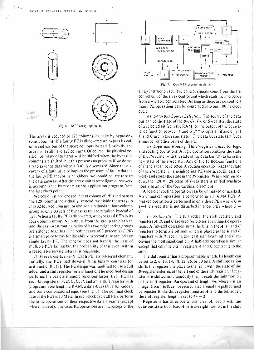


