Bipolar Transistor Operation - Carleton Universitytjs/16-bjtop.pdf · • Recall ideal diode...
25
Bipolar Transistor Operation 97.398*, Physical Electronics, Lecture 16
Transcript of Bipolar Transistor Operation - Carleton Universitytjs/16-bjtop.pdf · • Recall ideal diode...
Bipolar Transistor Operation
97.398*, Physical Electronics, Lecture 16

David J. Walkey 97.398*, Physical Electronics: Bipolar Operation (16) Page 2
Lecture Outline
• Last lecture discussed the structure and fabrication of a double diffused bipolar transistor
• Now examine current transfer in the bipolar structure in a qualitative way– Regions of operation: forward and reverse active, saturation and
cutoff – definitions, minority carrier density and current flow from quantitative point of view
– Calculate current components explicitly from minority carrier slopes (recall diffusion, lecture 7) – develop quantitative model equations next lecture
– Transistor Action: the basic mechanism which makes a bipolar useful in amplification
• Next lecture will derive quantitative relationships

David J. Walkey 97.398*, Physical Electronics: Bipolar Operation (16) Page 3
BJT Regions of Operation• The bipolar transistor has four
distinct regions of operation:– Forward Active– Reverse Active– Saturation– Cutoff

David J. Walkey 97.398*, Physical Electronics: Bipolar Operation (16) Page 4
pn-Junction Review• Recall that the boundary condition for the electron and hole minority
densities at the depletion region edges were npoeqVD/kT and pnoeqVD/kT
respectively, and that the minority density variation with distance is linear for a neutral region which is short compared to the minority diffusion length

David J. Walkey 97.398*, Physical Electronics: Bipolar Operation (16) Page 5
Forward Active Operation - Potentials• When the base-emitter junction
is forward biased and the base collector junction is reverse biased (implying VCE > VBE), the device is in the forward active region of operation

David J. Walkey 97.398*, Physical Electronics: Bipolar Operation (16) Page 6
Forward Active Operation - Minority Carriers• VBE > 0 raises pE(x) and nB(x) at the BE depletion region edges• VBC < 0 lowers pC(x) and nB(x) at the BC depletion region edges• Since all regions are short compared to the minority diffusion lengths,
the minority densities change linearly over all regions

David J. Walkey 97.398*, Physical Electronics: Bipolar Operation (16) Page 7
Forward Active Operation - Current Components• Three current components in forward active operation, all of which can
be characterised from the appropriate minority gradient:– “Linking current” due to electron transport from collector to emitter (1)– “Back injection” due to hole injection from base to emitter (2)– small component due to injection of holes from collector to base (3)

David J. Walkey 97.398*, Physical Electronics: Bipolar Operation (16) Page 8
Example 16.1: Current Calculations
• Calculate the electron and hole current densities flowing across the base-emitter junction for the device structure and bias condition shown below, using only the boundary conditions and the diffusion equation. The neutral widths were calculated in an earlier example.

David J. Walkey 97.398*, Physical Electronics: Bipolar Operation (16) Page 9
Example 16.1: Solution
• The required equations are the diffusion current density expressions
• and the minority carrier boundary conditions at the depletion edges of a pn-junction
J qDdn x
dxJ qD
dp xdxn n p p= = −
( ) ( )
p p e n n en noqV kT
p poqV kTD D
depl edge depl edge= =

David J. Walkey 97.398*, Physical Electronics: Bipolar Operation (16) Page 10
Example 16.1: Solution (con’t)• Applying these equations to the neutral emitter region gives
J qDdp x
dxqD
p p eW
e
p p pEo Eo
qV kT
E
BE
= − = −−
= − × ⋅ ⋅−
=−−
( )
. . .. .
16 10 12 221 21
1011219
0 8 0 026
4 A / cm2

David J. Walkey 97.398*, Physical Electronics: Bipolar Operation (16) Page 11
Example 16.1: Solution (con’t)• Applying the appropriate equations to the base neutral region with
VBC = -0.7V gives (note error in second gradient term in notes)
J qDdn x
dxqD
n e n eW
e e
n n nBo
qV kTBo
qV kT
B
BE BC
= =−
= × ⋅ ⋅× ⋅ − × ⋅
×= ×−
−
−
( )
. .. .
..
. . . .
16 10 34 921 10 21 10
14 102 28 1019
3 0 8 0 026 3 0 7 0 026
43 A / cm2

David J. Walkey 97.398*, Physical Electronics: Bipolar Operation (16) Page 12
Example 16.1: Solution (con’t)• Note that Jn, the electron injection (linking current) component, is
much larger than Jp, the hole (back) injection component
J Jn p= × =2 28 10 1123. . A / cm A / cm2 2

David J. Walkey 97.398*, Physical Electronics: Bipolar Operation (16) Page 13
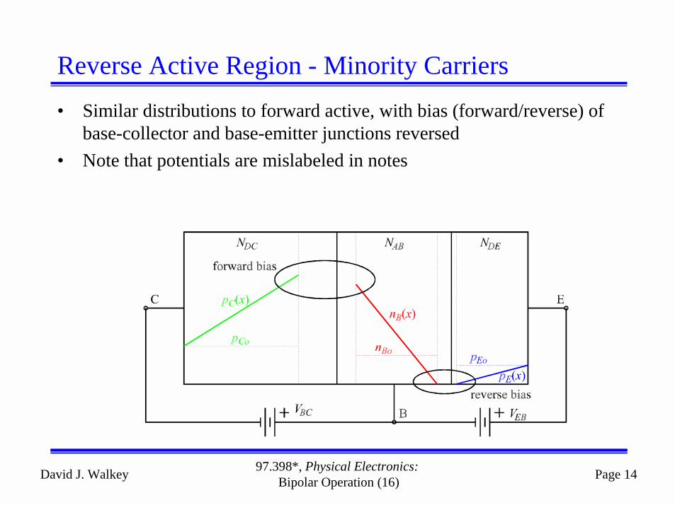
Reverse Active Region - Potentials• When the base collector
junction is forward biased and the base emitter junction is reverse biased (implying VEC > VBC), the device is in the reverse active region of operation
• Basically the forward active region with roles of emitter and collector reversed
David J. Walkey 97.398*, Physical Electronics: Bipolar Operation (16) Page 14
Reverse Active Region - Minority Carriers• Similar distributions to forward active, with bias (forward/reverse) of
base-collector and base-emitter junctions reversed• Note that potentials are mislabeled in notes

David J. Walkey 97.398*, Physical Electronics: Bipolar Operation (16) Page 15
Reverse Active Region - Current Components• Three current components in reverse active operation:
– “Linking current” due to electron transport from emitter to collector (1)– small component due to injection of holes from emitter to base (2)– “Back injection” due to hole injection from base to collector (3)

David J. Walkey 97.398*, Physical Electronics: Bipolar Operation (16) Page 16
Saturation Region - Potentials• The saturation region of
operation is characterised by forward bias potentials on both the base-emitter and base-collector junctions (implying VBE ≥ VCE)

David J. Walkey 97.398*, Physical Electronics: Bipolar Operation (16) Page 17
Saturation Region - Minority Carriers• With both junctions forward biased, the minority carrier densities are
raised above their equilibrium values throughout the device• The values of nB(x) on either side of the neutral base region (nBoeqVBE/kT
and nBoeqVBC/kT) determine the slope of nB(x) - depending on the relative values of VBE and VBC, the slope may be +ve, -ve or zero

David J. Walkey 97.398*, Physical Electronics: Bipolar Operation (16) Page 18
Saturation Region - Current Components• Three current components in saturation operation:
– “Linking current” due to electron transport (1) - can be from emitter to collector (VBE < VBC), collector to emitter (VBE > VBC), or zero (VBE = VBC)
– component due to injection of holes from base to emitter (2)– component due to injection from base to collector (3)

David J. Walkey 97.398*, Physical Electronics: Bipolar Operation (16) Page 19
Cutoff Region - Potentials• When both junctions are reverse
biased (implying VBE negative and VBE ≥ VCE) the device is in the cutoff region of operation

David J. Walkey 97.398*, Physical Electronics: Bipolar Operation (16) Page 20
Cutoff Region - Minority Carriers
• With VBE and VBC reverse biased, the minority carrier densities are small at all depletion region edges
• This implies that nB(x) is zero over the entire neutral base region, since the distribution must be linear

David J. Walkey 97.398*, Physical Electronics: Bipolar Operation (16) Page 21
Cutoff Region - Current Components• Only two current components in saturation operation - “linking
current” is zero because gradient of nB(x) is zero – small component due to injection of holes from emitter to base (2)– small component due to injection from collector to base (3)

David J. Walkey 97.398*, Physical Electronics: Bipolar Operation (16) Page 22
pn-Junction - Current Components• Recall ideal diode equation saturation current density for p+n diode
• When one doping is much higher than the other, injection into the more lightly doped side dominates (equilibrium density much higher)
JqD n
wqD p
LS p n
n po
p
p no
p+ = +

David J. Walkey 97.398*, Physical Electronics: Bipolar Operation (16) Page 23
Transistor Action
• The term transistor action refers to the control of the large collector-emitter (linking) current by the smaller base (back injection) current in forward active operation, the origin of “current gain” in a BJT
• Two features of the device are essential for transistor action– a narrow base, which forces all electrons injected from the emitter
to travel across the base neutral region to the collector– a high emitter doping compared to the base doping, making base
(electron) injection the dominant term

David J. Walkey 97.398*, Physical Electronics: Bipolar Operation (16) Page 24
Transistor Action in Forward Active Operation• Current components across base-emitter junction are related by relative
doping• Large collector to emitter current controlled by small (back injection)
base current due to requirement for relation across BE junction• Narrow base prevents flow of injected electrons out base lead
David J. Walkey 97.398*, Physical Electronics: Bipolar Operation (16) Page 25
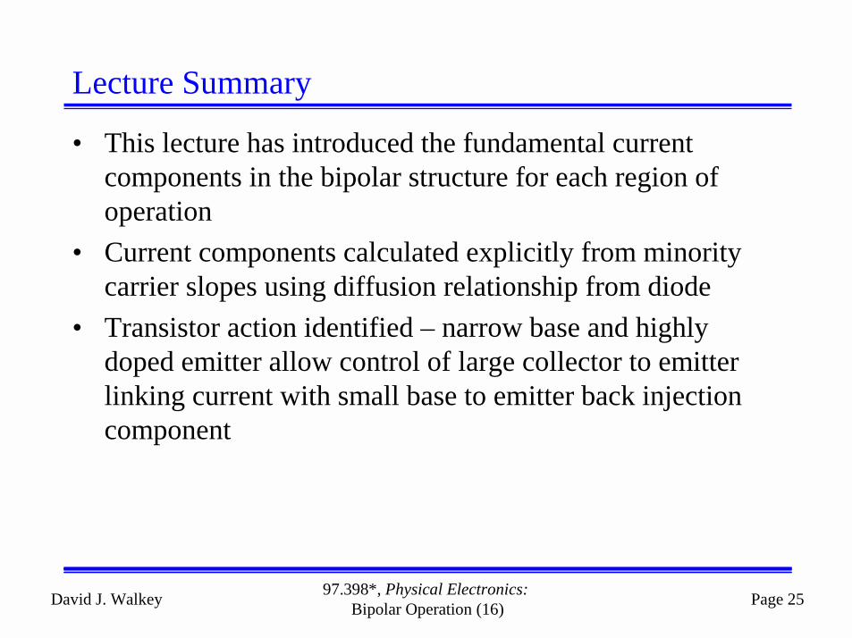
Lecture Summary
• This lecture has introduced the fundamental current components in the bipolar structure for each region of operation
• Current components calculated explicitly from minority carrier slopes using diffusion relationship from diode
• Transistor action identified – narrow base and highly doped emitter allow control of large collector to emitter linking current with small base to emitter back injection component