Bipolar Resistive Switching of Bi-Layered Pt/Ta O /TaO /Pt ...
153
DEPARTMENT OF ELECTRICAL AND ELECTRONIC ENGINEERING Bipolar Resistive Switching of Bi-Layered Pt/Ta 2 O 5 /TaO x /Pt RRAM – Physics-based Modelling, Circuit Design and Testing. Ph.D Candidate Firas Odai Hatem Supervisor Dr. T. Nandha Kumar Co-Supervisor Prof. Haider Abbas Mohammed Almurib DATE OCTOBER 2016 A PhD thesis submitted in part fulfilment of the requirements for the degree of Doctor of Philosophy (Ph.D) [Electrical and Electronic Engineering], The University of Nottingham.
Transcript of Bipolar Resistive Switching of Bi-Layered Pt/Ta O /TaO /Pt ...
DEPARTMENT OF ELECTRICAL AND ELECTRONIC ENGINEERING
Bipolar Resistive Switching of Bi-Layered Pt/Ta2O5/TaOx/Pt RRAM – Physics-based Modelling, Circuit Design and Testing.
Ph.D Candidate Firas Odai Hatem Supervisor Dr. T. Nandha Kumar Co-Supervisor Prof. Haider Abbas Mohammed Almurib DATE OCTOBER 2016
A PhD thesis submitted in part fulfilment of the requirements for the degree of Doctor of Philosophy (Ph.D)
[Electrical and Electronic Engineering], The University of Nottingham.
I
TABLE OF CONTENTS
1. Chapter One: Introduction .......................................................................................................................................... 1
1.1. Resistive Random Access Memory Devices ................................................................................................. 1
1.2. Research Gap in the Field of RRAM Devices .............................................................................................. 3
1.3. Motivation and Contributions to Develop a Mathematical Bi-Layered Ta2O5/TaOx RRAM Model–Research First Stage ................................................................................................................................................... 5
1.3.1. Modelling of TPF ................................................................................................................................. 5 1.3.2. Modelling the Continuous Charging and Discharging of the Interface Traps ..................................... 6 1.3.3. Modelling of Electric Field and Ions Migration Mechanism ............................................................... 7
1.4. Motivation and Contributions to Develop a SPICE Ta2O5/TaOx bi-layered RRAM Model – Research Second Stage .............................................................................................................................................................. 7
1.5. Aims and Objectives of the Research ........................................................................................................... 9 1.5.1. Aims and Objectives of the First Stage ................................................................................................ 9 1.5.2. Aims and Objectives of the Second Stage .......................................................................................... 10
1.6. Methodology ............................................................................................................................................... 11 1.6.1. Mathematical and SPICE Modelling .................................................................................................. 11 1.6.2. Model Validation and Evaluation Steps ............................................................................................. 12
2. Chapter Two: Preliminaries on the Memristor / RRAM Devices ........................................................................ 14
2.1. The First fabricated memristor (HP Labs memristor) and its Operating Mechanism ................................. 14
2.2. Pre-Resistive Switching Process (Electroforming Process) and the Resistive Switching Mechanism of the MIM RRAM Devices ............................................................................................................................................... 19
2.3. The Effect of the Device Area on the Produced Gas Bubbles and The Physical Deformation .................. 21
2.4. The Effect of the Asymmetry of the Metal/Oxide interfaces on the Forming Voltage .............................. 25
2.5. Overall Summary of the Electroforming Step ............................................................................................. 26 2.5.1. Electroforming the RRAM Device into ON Initial State ................................................................... 26 2.5.2. Electroforming the RRAM Device into OFF Initial State .................................................................. 26
3. Chapter Three: Literature Review on the MIM and MISM RRAM Models ....................................................... 28
3.1. MIM Mathematical and SPICE RRAM Models ......................................................................................... 28
3.2. Bi-layered RRAM ANALYTICAL AND SPICE Models .......................................................................... 35
4. Chapter Four: Mathematical Modelling of the Pt/Ta2O5/TaOx/Pt Bi-Layered RRAM ....................................... 47
4.1. The Structure and the Semiconductor Properties of the Pt/Ta2O5/TaOx/Pt RRAM Proposed Model ........ 49 4.1.1. The Structure of the Proposed Model ................................................................................................. 49 4.1.2. The Bipolar Resistive Switching Mechanism of the Proposed Model ............................................... 49
4.2. Modelling Of The un-Doped Region Evolution Stages .............................................................................. 51 4.2.1. Modelling of Oxygen Ion Migration for Ta2O5/TaOx RRAM ........................................................... 51 4.2.2. Modelling of the Un-Doped Region Dynamics During the Simulation ............................................. 53 4.2.3. Electric Field Modelling for the Proposed Model .............................................................................. 54 4.2.4. The Electric Field Threshold and the Self-limiting Effect During Switching Into LRS .................... 55 4.2.5. The Electric Field Threshold and the Self-limiting Effect During Switching Into HRS ................... 57
4.3. Current–Voltage Behaviour ........................................................................................................................ 58 4.3.1. Current Transport Process in the Proposed Mathematical Model ...................................................... 58
II
4.3.2. Adding the Effect of the Insulator Layer–TPF ................................................................................... 59 4.3.3. The Effect of the Continuous Charging–Discharging of the Interface Traps on the I–V Behaviour . 62 4.3.4. Adding the Effect of the Image Force Lowering Factor and the Doping Level Variation on Schottky Barrier 66
4.4. Temperature Modelling ............................................................................................................................... 68
4.5. Bi-Layered RRAM Device Simulation and Results Discussion ................................................................. 69 4.5.1. Relationship and the Agreement with the LRS/HRS Switching Behaviour ...................................... 69
4.5.1.1. Non-Linear Ionic Drift Mechanism ............................................................................................... 69 4.5.1.2. Ideal State – Linear Dopant Drift ................................................................................................... 72
4.5.2. The Complete Evolution of w, ∅b–V, and Rseries–V ....................................................................... 73 4.5.3. Electric Field Effect ............................................................................................................................ 74 4.5.4. The Effect of Adding TPF to the RRAM I–V Characteristic Equation ............................................. 77 4.5.5. The Agreement of the Proposed Model to the Attributes of the Zero-Crossing Behaviour for the Memristive System .............................................................................................................................................. 78
5. Chapter Five: SPICE Modelling of Ta2O5/TaOx Bi-Layered RRAM .................................................................. 79
5.1. The Structure of the Proposed Model and its Bipolar Resistive Switching Mechanism ............................ 82
5.2. SPICE Model Implementation .................................................................................................................... 84 5.2.1. Current Path SPICE Subcircuit .......................................................................................................... 87 5.2.2. w and E Evolution Dynamics SPICE Subcircuit ................................................................................ 88
5.3. Model Evaluation and Simulation Studies .................................................................................................. 89 5.3.1. The Agreement with the I–V Characteristics for Different Values of D ........................................... 89 5.3.2. The Dependency of HSV and LSV on D ........................................................................................... 93 5.3.3. The Effects of Changing D on the Values of LRS and HRS .............................................................. 94 5.3.4. The Intrinsic Schottky Barrier and its Effect on the HRS During SET Switching ............................ 96 5.3.5. Testing the Model under Different Types of Input Signals ................................................................ 98 5.3.6. RRAM-Based Non-Volatile D-Latch ............................................................................................... 102 5.3.7. Computational Efficiency ................................................................................................................. 105 5.3.8. Testing the Applicability of the Proposed Model for simulation of RS Behaviour ......................... 105
6. Chapter Six: A Predictive Compact SPICE Model of TaOx-Based MIM RRAM ............................................. 108
6.1. The Structure and the RS Mechanism of the Proposed MIM SPICE Model ............................................ 109
6.2. Modelling of the Dynamic Behavior – SET and RESET Processes ......................................................... 110
6.3. Modelling of the Static Behavior – Current Conduction Process ............................................................. 112
6.4. SPICE Model Implementation .................................................................................................................. 113
6.5. Model Evaluation and Simulation Studies ................................................................................................ 116
7. Conclusion and Future Work ............................................................................................................................. 119
8. References .......................................................................................................................................................... 121
9. Appendix A ........................................................................................................................................................ 126
9.1. MATLAB Scripts for the Proposed MISM Mathematical RRAM Model Presented in Chapter Four ..... 126 9.1.1. MATLAB Script for D = 4 nm ......................................................................................................... 126 9.1.2. MATLAB Script for D = 3 nm ......................................................................................................... 131
9.2. SPICE Subcircuits for the Proposed MISM SPICE RRAM Model Presented in Chapter Five. .............. 135 9.2.1. SPICE Subcircuit for D = 4 nm. ....................................................................................................... 135 9.2.2. SPICE Subcircuit for D = 3 nm. ....................................................................................................... 137
III
LIST OF FIGURES
Figure 1.1. TEM image of (a) Pt/Ta2O5/TaOx/Pt bi-layered RRAM film and (b) Pt/TaOx/Pt MIM RRAM film. ......... 4
Figure 2.1. The four two-terminal fundamental circuit elements and their related six equations [9]. ......................... 15
Figure 2.2. (a) The memristor I–V characteristics loops for two different frequencies (b) The memristor applied
sinusoidal voltage v0sin(w0t) and the resulting current as a function of time for the memristor device in [9]. ............ 16
Figure 2.3. A simple equivalent circuit of the variable-resistor model of HP memristor. ............................................ 18
Figure 2.4. The ideal reversible BRS process and the required forming voltage polarity. ........................................... 20
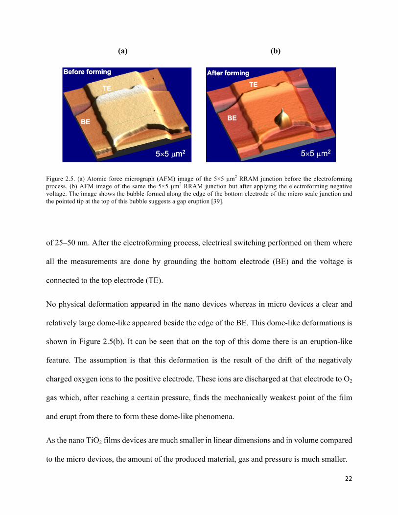
Figure 2.5. (a) AFM image of the 5×5 µm2 RRAM junction before the electroforming process. (b) AFM image of the
same the 5×5 µm2 RRAM junction but after applying the electroforming negative voltage.. ..................................... 22
Figure 2.6. The behaviour of the gas bubbles during electroforming process and under different bias polarities ....... 23
Figure 2.7. Electroforming dependency of the applied bias polarity on the TE ........................................................... 24
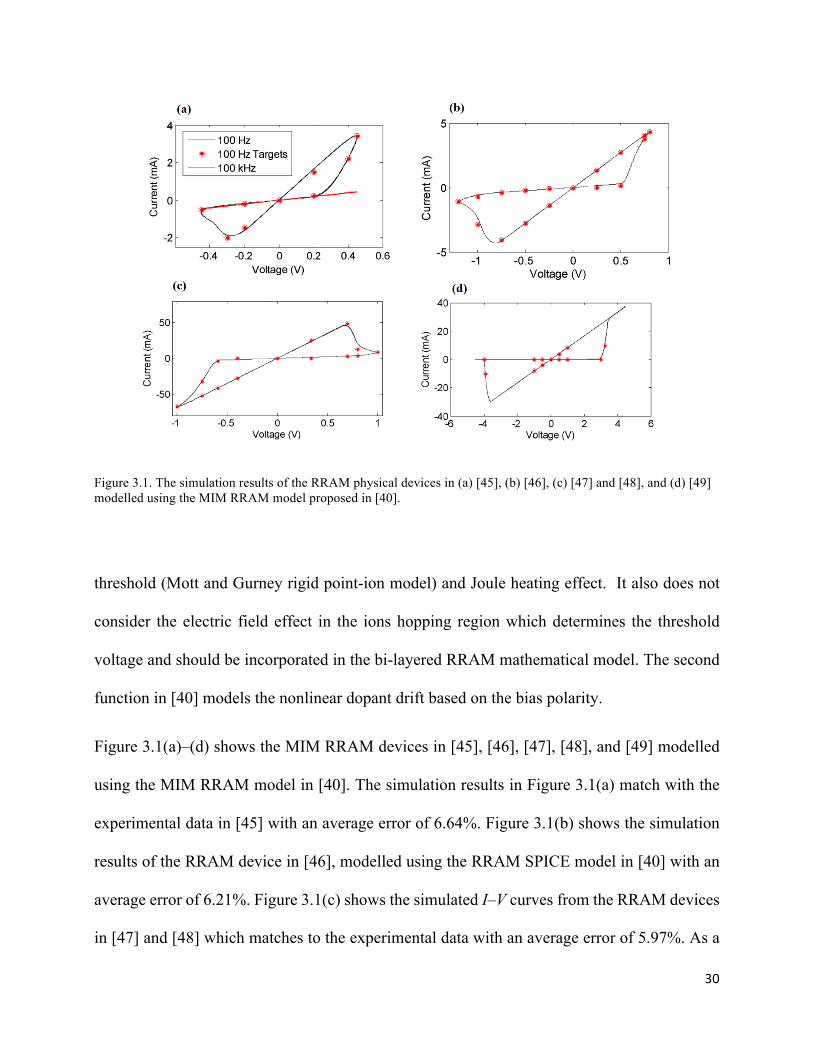
Figure 3.1. The simulation results of the RRAM physical devices in (a) [45], (b) [46], (c) [47] and [48], and (d) [49]
modelled using the MIM RRAM model proposed in [40]. .......................................................................................... 30
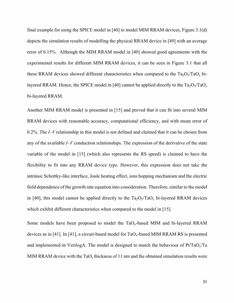
Figure 3.2. The Equivalent circuit model and the cell structure of the Pt/TaOx/Ta MIM RRAM model in [41]. ....... 32
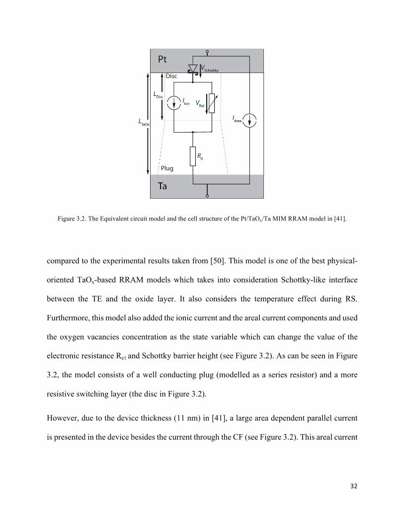
Figure 3.3. The measured I–V characteristics from [50] and the simulation results in [41] for the Pt/TaOx/Ta MIM
RRAM device with TaOx thickness of 11 nm .............................................................................................................. 33
Figure 3.4. The typical I–V characteristics of the HfOx/AlOx RRAM measured by DC sweep. ................................ 35
Figure 3.5. 3-D Evolution dynamics of the SET and RESET process of the model in [25]. ....................................... 36
Figure 3.6. (a) The current conduction mechanism in the CF and the gap regions of the model in [25]. (b) The simulation
results and the measured data of TiN/HfOx/AlOx/Pt bi-layered RRAM from [24]. .................................................... 37
Figure 3.7. (a) Cross-sectional field-emission TEM of the AlOx/WOx bi-layered RRAM device in [22]. (b) I–V
characteristics of different resistance state .................................................................................................................. 38
Figure 3.8. (a) Cross-sectional TEM image of the RRAM device in [22]. (b) AES depth analysis of the bi-layered
RRAM in [22]. .............................................................................................................................................................. 39
Figure 3.9. (a) Cross section of the bi-layered RRAM cell simulated in [18]. (b) The simulation results and the measured
I–V characteristics as reported in [18] .......................................................................................................................... 42
IV
Figure 3.10. (a) The equivalent circuit used in the model in [16]. (b) The doped region thickness w normalized to D in
response to a sinewave signal. ...................................................................................................................................... 43
Figure 3.11. (a) The simulation results and (b) the measured data of the model in [16]. ............................................. 45
Figure 4.1. A schematic representation of the proposed mathematical RRAM model and its BRS mechanism. (a) The
LRS and (b) the HRS. ................................................................................................................................................... 50
Figure 4.2. Experimental measurements [16] and the semi-log scale plot of the modelling results I–V characteristics
with D = 4 nm. .............................................................................................................................................................. 70
Figure 4.3. Semi-log scale plot of the I–V characteristics of the proposed RRAM model using linear dopant drift .. 71
Figure 4.4. Calculated w normalized to D and the total applied bias as a functions of time [16]. ............................... 72
Figure 4.5. The simulation results of (a) The voltage dependence plot of 𝑅𝑠𝑒𝑟𝑖𝑒𝑠 (b) The barrier height against V. 73
Figure 4.6. Simulated 𝐸–𝑉 characteristics in semi-log scale plot for the complete evolution of 𝐸 and (inset) 𝐸–𝑤
simulation in linear scale. ............................................................................................................................................. 75
Figure 4.7. (a) Simulation results of I–V curve in semi-log scale plot and (b) Simulated linear I–V and 𝑤–𝑉 curves for
the LRS→HRS switching stage. ................................................................................................................................... 76
Figure 4.8. Experimental measurements [17] and the semi-log scale plot of the modelling results I–V characteristics
with D = 3 nm. .............................................................................................................................................................. 77
Figure 5.1. A schematic representation of the proposed SPICE model and its switching mechanism. (a) The LRS and
(b) the HRS. .................................................................................................................................................................. 82
Figure 5.2. LTSPICE implementation of the proposed SPICE model. (a) The two terminal (current path) SPICE
implementation. (b) The SPICE subcircuit implementation of 𝑤 evolution, 𝐸, and the self-limiting effect. .............. 85
Figure 5.3. LTSPICE subcircuit implementation of the proposed bi-layered RRAM SPICE model. .......................... 86
Figure 5.4. Experimental measurements [16] and the semi-log scale plot of the SPICE model simulation I–V
characteristics ................................................................................................................................................................ 90
Figure 5.5. Experimental measurements [17] and the semi-log scale plot of the SPICE model simulation I–V
characteristics ............................................................................................................................................................... 91
Figure 5.6. Experimental measurements [16] and the linear scale plot of the SPICE model simulation I–V
characteristics ................................................................................................................................................................ 92
V
Figure 5.7. The semi-log scale plot of the SPICE model simulation I–V characteristics with D = 3 nm, ∅𝐵𝑛0 = 0.45𝑒𝑉
(blue line) and D = 4 nm, ∅𝐵𝑛0 = 0.6𝑒𝑉 (red line). ................................................................................................... 93
Figure 5.8. (a) The SPICE model simulation of the device total resistance 𝑅𝑠𝑒𝑟𝑖𝑒𝑠 + 𝑉𝑆/𝐼 (blue line) and the total
current 𝐼 (purple line) as a function of time for the 4 nm Ta2O5 layer thickness (b) The corresponding variation in ∅𝑏,
TPF, 𝑉𝑆, and 𝑉. ............................................................................................................................................................. 96
Figure 5.9. The SPICE model simulation of the device total resistance 𝑅𝑠𝑒𝑟𝑖𝑒𝑠 + 𝑉𝑆/𝐼 (blue line) and the applied
voltage 𝑉 (red dashed line) as a function of time for D = 4 nm. (b) 3/-2 V with a period of 10 ms rectangular wave bias
signal. ............................................................................................................................................................................ 99
Figure 5.10. (a) Experimental measurements of the Ta2O5/TaOx bi-layered RRAM [17] and simulation results of the
proposed SPICE model for RESET pulse switching operation with D = 3 nm. (b) Time domain response simulation of
the current compared with the measured current at HRS (IHRS) (c) Time domain response simulation of the resistance
compared with the experimental resistance at HRS. .................................................................................................. 101
Figure 5.11. Schematic of the RRAM-based NV D-Latch with the Ta2O5/TaOx RRAM SPICE model integrated. . 103
Figure 5.12. The SPICE simulation of the RRAM-based NV D-Latch (a) with the Ta2O5/TaOx RRAM SPICE model
integrated and (b) without the RRAM connected. ...................................................................................................... 104
Figure 5.13. Sweep rate dependency of the I–V characteristic of the proposed SPICE model. ................................. 106
Figure 6.1. Schematic representation of the Ta/TaOx/Pt MIM RRAM cell modelled .............................................. 109
Figure 6.2. LTSPICE implementation of the proposed MIM SPICE model. (a) The two terminal (current path) SPICE
implementation (b) The SPICE subcircuit implementation of 𝑦 evolution. ............................................................... 115
Figure 6.3. LTSPICE subcircuit implementation of the proposed MIM SPICE model. ............................................ 116
Figure 6.4. The linear scale plot of the MIM SPICE model simulation I–V characteristics ...................................... 117
VI
LIST OF TABLES
Table 5-1. The equations used in the SPICE RRAM model, extracted from the RRAM mathematical model . ......... 83
Table 5-2. Parameters used in the proposed SPICE RRAM model simulation for D = 4 nm and 3 nm. ..................... 84
Table 6-1. Parameters used in the proposed MIM SPICE RRAM model simulation. ............................................... 114

VII
LIST OF ABBREVIATIONS
Acronym Description NVM Non-Volatile Memory
MRAM Magnetic Random Access Memory PRAM Phase-Change Random Access Memory FRAM Ferroelectric Random Access Memory SRAM Static Random Access Memory DRAM Dynamic Random Access Memory RRAM Resistive Random Access Memory
RS Resistive Switching BRS Bipolar Resistive Switching NV Non-Volatile
MIM Metal-Insulator-Metal MISM Metal-Insulator-Semiconductor-Metal HRS High Resistance State LRS Low Resistance State TEM Transmission Electron Microscopy TPF Tunnelling Probability Factor CF Conductive Filament
HSV High Resistance State Switching Voltage BE Bottom Electrode TE Top Electrode
AFM Atomic Force Micrograph LSV Low Resistance State Switching Voltage
VCCS Voltage-Controlled Current Source VCVS Voltage-Controlled Voltage Source OCF Outside the CF
VIII
LIST OF PUBLICATIONS
Peer Reviewed Journal Articles
1. F. O. Hatem, T. N. Kumar, and H. A. F. Almurib, “A SPICE Model of the Ta2O5/TaOx Bi-Layered RRAM,” IEEE Transactions on Circuits and Systems I: Regular Papers, vol. 63, no. 9, pp. 1487–1498, Sept. 2016.
2. F. O. Hatem, P. W. C. Ho, T. N. Kumar, and H. A. F. Almurib, “Modeling of bipolar resistive switching of a nonlinear MISM memristor,” Semiconductor Science and Technology, vol. 30, no. 11, p. 115009, Oct. 2015.
3. P. W. C. Ho, F. O. Hatem, T. N. Kumar, and H. A. F. Almurib, “Comparison between Pt/TiO2/Pt and Pt/TaOX/TaOY/Pt based Bipolar Resistive Switching Devices,” J. Semicond., vol. 37, no. 6, p. 064001, June 2016.
Peer Reviewed Conference Proceedings
4. P. W. C. Ho, F. O. Hatem, T. N. Kumar, and H. A. F. Almurib, “Enhanced SPICE memristor model with dynamic ground,” in Proc. IEEE Int. Circuits and Syst. Symposium, Sep. 2015, pp. 130-132.
5. P. W. C. Ho, F. O. Hatem, T. N. Kumar, and H. A. F. Almurib, “Comparison on TiO2 and TaO2 based bipolar resistive switching devices,” in Proc. 2014 2nd Int. Conference on Electronic Design, Aug. 2014, pp. 249-254.
PeerReviewedPosterPresentations6. F. O. Hatem, T. N. Kumar, and H. A. F. Almurib, “Ph.D Thesis: Bipolar Resistive
Switching ofBi-LayeredPt/Ta2O5/TaOx/PtRRAM–Physics-basedModelling, CircuitDesignandTesting,”inDesign,Automation&TestinEuropeConferenceandExhibition(DATE),Lausanne,Switzerland,Mar.2017.
Publications in Preparation
7. A journal paper titled “Compact SPICE Model of Ta/TaOx/Pt MIM RRAM” is currently in preparation and will be submitted to one of the related journals.
8. A conference paper based on using the proposed bi-layered RRAM SPICE model developed during this research in a RRAM-based circuit application. The paper will be submitted for presentation to an IEEE related conference.
IX
LIST OF AWARDS

X
ACKNOWLEDGMENT
First and foremost, I am thankful to Almighty Allah for blessing, protecting and guiding me to complete this Ph.D
Thesis. I could never have finished this work without the faith I have in the Allah.
I would like to express my special appreciation and thanks to my supervisors: Dr. T. Nandha Kumar and Prof. Haider
Abbas Almurib who introduced me to this interesting field of Resistive Random Access Memories and provided me
this invaluable opportunity to work under their kind supervision. They have been a tremendous mentor for me and I
am thankful to them for all their guidance throughout the four years’ period that I spent doing this research. Their
constructive comments and proposed solutions during the various research stages and also during the publication stage
resulted in the success of this Ph.D research and in publishing it in a reputed peer reviewed journals. I will always
remember Dr. Nandha for his patience with me at the difficult times, and for treating me not like a student, but like his
brother and friend and for introducing me to his lovely family. I could not have imagined having a better experienced
supervisor for my Ph.D study. Also, I will always remember Prof. Haider’s words: “There is nothing impossible in this
life!”. The advices that Dr. Nandha and Prof. Haider gave me during the time I spent with them have been priceless
and will help me a lot during my future career.
Also, I would like to thank my thesis moderator and internal examiner: Dr. Anandan Shanmugam for meeting me and
giving me some of his valuable time and for his questions which helped me to widen my research from various
perspectives. I also thank him for his understanding when my research nearly stopped for few months due to
unexpected visa issues.
Most importantly, none of this work would have been possible without my family, to whom this thesis is dedicated.
My deepest gratitude goes to my wonderful parents and my two beloved sisters for their endless love, constant support,
patient and motivation at all times in my life. Mama and Papa, Ghada and Marwa, a million thanks to you. I love you
so much.
Finally, I would like to give my love and my heartiest thanks to my beloved fiancée, Marwa, for her love, prayers and
encouragement. She was always there stood by me through the good and bad times. I have no suitable word to describe
my everlasting love to her and words cannot express how grateful I am for her being with me all the time. I would like
to express my love to her for spending sleepless nights with me and was always my support in the moments when there
was no one around. One of the biggest motivations that helped me to finish this research is to meet her and plan my
life together with her. Marwa, I love you.
Firas Odai Hatem, October 2016.
XI
ABSTRACT
Over the last few years, the non-volatile memories (NVM) have been dominating the research of
the storage elements. The resistance random-access memory (RRAM) and the memristor that
employs the resistive switching (RS) mechanism appear to be potential candidates for NVM.
Among the RS materials that were reported is the TaOx which showed surprising RS performance.
This oxide material has been widely used to construct a metal-insulator-semiconductor-metal
(MISM) RRAM which can be referred to as bi-layered RRAM. This bi-layered RRAM consists of
TaOx as a bulk material and Ta2O5 as an insulator layer, sandwiched between two platinum
electrodes to form Pt/Ta2O5/TaOx/Pt RRAM. However, a physics-based mathematical model of
this RRAM is required to further study the detailed physics behind its conduction mechanism and
the RS process. In addition to the mathematical model, a SPICE model is also required to
understand the behaviour of this bi-layered RRAM device when integrated in memory design for
the future generation storage devices or when used in RRAM-based circuit applications.
This doctoral research presents novel mathematical and SPICE models of a bipolar resistive
switching (BRS) of the Pt/Ta2O5/TaOx/Pt bi-layered RRAM. For this purpose, MATLAB and
LTSPICE are used to design the mathematical and the SPICE bi-layered RRAM models,
respectively, and the obtained simulation results for both models are compared with the
experimental data from SAMSUNG labs.
The novelty of the mathematical model lies in incorporating the tunnelling probability factor (TPF)
between the semiconductor and the metal layers and therefore, demonstrating its effect on the
conduction mechanism. In addition, the effect of continuous variation of the interface traps
densities and the ideality factor during BRS is modelled using the semiconductor properties and
XII
the characteristics of the metal-insulator-semiconductor (MIS) system. Thus, the model
emphasizes the dependency of the device current on the physical characteristics of the insulator
layer. Moreover, the electric field equation for the active region is derived for the MISM structure
which is used together with Mott and Gurney rigid point-ion model and Joule heating effect to
model the oxygen ion migration mechanism. Finally, the model also demonstrates the self-limiting
growth of the doped region.
The proposed SPICE model emphasizes the impact of the change in the switching layer thickness
on the device behaviour at low resistance state (LRS), high resistance state (HRS), and the
transitional period. The validity of the SPICE model is verified through using three different sets
of experimental data from Pt/Ta2O5/TaOx/Pt RRAM with switching layer thickness smaller than 5
nm. The SPICE model reproduced all the major features from the experimental results for the SET
and RESET processes and also the asymmetric and the symmetric characteristics in HRS and LRS,
respectively. The SPICE model matches the measured experimental results with an average error
of < 11%. It also showed stable behaviour for its HRS and LRS regions under different types of
input signals. The model is parameterized in order to fit into Ta2O5/TaOx RRAM devices with
switching layer thickness smaller than 5 nm, thus, facilitating the model usage. The SPICE model
can be included in the SPICE-compatible circuit simulation and is suitable for the exploration of
the Ta2O5/TaOx bi-layered RRAM device performance at circuit level.
At the end of the research, a metal-insulator-metal (MIM) RRAM SPICE model of Ta/TaOx/Pt is
developed which can be used in the future work to compare between the MISM and MIM TaOx-
based RRAM devices.
1
1. Chapter One
INTRODUCTION
1.1. Resistive Random Access Memory Devices
Over the last few years, the non-volatile memories (NVM) have been dominating the research
of the storage elements [1], [2]. Examples of such memories are the magnetoresistive random-
access memory (MRAM) [3], phase-change random-access memory (PRAM) [4], and
ferroelectric random-access memory (FRAM) [5]. These candidates aim for the replacement
of the conventional semiconductor memories such as Si charge-based flash memory, static
random-access memory (SRAM), and dynamic random-access memory (DRAM) [6].
However, considering the future NVM at nanoscale range requires switching mechanism to be
operating in the range of at least 10–30 nm technology with switching current in the range of
10–100 µA [1], PRAM has a problem with the switching current condition [4] while FRAM
and MRAM appear to have limitations with the scaling [5]. At the same time, the flash memory
has also been lacking in achieving some of the important future NVM requirements (e.g.,
switching speed, retention time, and the number of WRITE–ERASE cycles) [1].
2
Alternatively, metal-oxide bipolar resistive random-access memory (RRAM) and the
memristor that employs resistive switching (RS) mechanism appear to be a potential candidates
for the next generation NVM [1], [7], [8], [9] and their applications [10], [11], [12], [13].
RRAM devices can be considered as a specific type of the memristors which can describe the
bipolar resistive switching (BRS) behaviour [9], [14]. RRAM devices demonstrate various
characteristics and attributes which make it useful element for logic circuit design,
neuromorphic systems, and memory applications such as high density cross bar memories. For
example, RRAM provide non-volatile (NV) characteristics, fast write and read time and it has
a non-destructive reading mechanism where the stored data is ideally not altered (or slightly
altered) during the reading mechanism [15]. RRAM devices exhibit the non-destructive
behaviour because its state variable change slightly in the case of low current (reading current)
while the change due to high current is significantly larger. In other words, the RRAM state
variable has a nonlinear dependence on the charge [15]. In addition, RRAM provides high
ROFF/RON ratio in order to store distinct Boolean data where ROFF and RON are the RRAM
resistances at high resistance state (HRS) and low resistance state (LRS), respectively. In
general, when storing a digital state into a certain memory device, it is important for the stored
data to be distinct. This means that the differences between the stored data are considerably
large. By doing this, we guarantee that the digital stored state is not sensitive to the changes in
both the operating conditions and the parameters [15]. In addition to these characteristics,
RRAM devices demonstrate a good scalability and low power consumption.
Knowing that the RRAM devices exhibit all these useful characteristics which makes it an
important device for the potential circuits applications, especially NVM, a great appreciation
3
and interest has been developed in this field which led to the start of this doctoral research.
Also, knowing that the leading companies in the field (SAMSUNG, Hewlett Packard, Micron,
IBM, Panasonic…etc.) are currently carrying out research and developments on these
promising memory candidates, an excellent research opportunity arises for conducting more
explorations and experiments in this promising field.
1.2. Research Gap in the Field of RRAM Devices
Based on their structure, RRAM devices can be classified into metal-insulator-metal (MIM)
[7] and metal-insulator-semiconductor-metal (MISM) RRAM devices [1], [8] hereafter will be
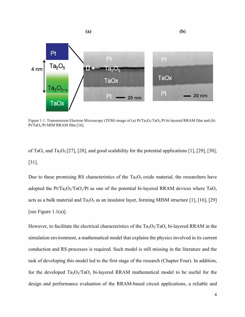
referred to as bi-layered RRAM. A typical tantalum oxide-based MISM and MIM RRAM
physical devices are shown in Figure 1.1(a) and (b), respectively [16].
Recently, the bi-layered RRAM has been extensively studied as one of the promising
candidates for the NVM [1], [8], [16], [17], [18], [19], [20], [21], [22], [23], [24], [25], [26].
As can be seen in Figure 1.1(a), typical bi-layered RRAM device comprises a bulk layer and a
more RS oxide layer, sandwiched between two metal electrodes [8]. Different RS oxide
materials have been reported for the bi-layered RRAM devices such as: AlOx/WOx [22],
CuO/ZnO [23], HfOx/AlOx [24] and [25], TiOx/HfOx [26], and Ta2O5/TaOx [1], [8], [16], [17],
[18], [19], [20], [21]. Among these materials, Ta2O5 is considered as one of theprospective RS
materials which attracted increasing research interest and showed surprising performance. In
particular, it exhibited an extreme cycling endurance of over 1012, an improved retention time
of more than 10 years, an abrupt switching time (< 1 ns), multilevel states, two stable phases
4
(a) (b)
Figure 1.1. Transmission Electron Microscopy (TEM) image of (a) Pt/Ta2O5/TaOx/Pt bi-layered RRAM film and (b) Pt/TaOx/Pt MIM RRAM film [16].
of TaOx and Ta2O5 [27], [28], and good scalability for the potential applications [1], [29], [30],
[31].
Due to these promising RS characteristics of the Ta2O5 oxide material, the researchers have
adopted the Pt/Ta2O5/TaOx/Pt as one of the potential bi-layered RRAM devices where TaOx
acts as a bulk material and Ta2O5 as an insulator layer, forming MISM structure [1], [16], [29]
[see Figure 1.1(a)].
However, to facilitate the electrical characteristics of the Ta2O5/TaOx bi-layered RRAM in the
simulation environment, a mathematical model that explains the physics involved in its current
conduction and RS processes is required. Such model is still missing in the literature and the
task of developing this model led to the first stage of the research (Chapter Four). In addition,
for the developed Ta2O5/TaOx bi-layered RRAM mathematical model to be useful for the
design and performance evaluation of the RRAM-based circuit applications, a reliable and
5
predictive SPICE model of this device is required which also still missing in the available
literatures. The task of developing this RRAM SPICE model led to the second stage of this
research (Chapter Five).
1.3. Motivation and Contributions to Develop a Mathematical Bi-Layered Ta2O5/TaOx RRAM Model–Research First Stage
Despite the advances in the Ta2O5/TaOx bi-layered RRAM models [8], [16], [17], [18], [19],
[20] and other bi-layered RRAM models based on different materials (e.g. Al/AlOx/WOx/W)
[22], a new physics-based mathematical model is required to further study the detailed physics
behind the conduction mechanism (static behaviour) and the evolution of the doped region
(dynamic behaviour) in the Ta2O5/TaOx bi-layered RRAM. In the first stage of this research, a
novel physics-based model that describes the BRS behaviour in the Ta2O5/TaOx bi-layered
RRAM is presented (Chapter Four). The proposed model is developed based on the MIS system
behaviour. It also comprises the physical characteristics of the Ta2O5 insulator layer by
considering: (1) The tunnelling probability factor (TPF) and (2) The continuous charging and
discharging of the interface traps. In addition, the proposed model also (3) derives the electric
field equation for the ions hopping switching region in order to predict the oxygen ion
migration mechanism. The main three contributions of the first stage are listed below.
1.3.1. Modelling of TPF
At high field, the presence of the insulator layer in the MIS system has certain effects on the
device behaviour. First, it leads to the modification the TPF: a term in the current conduction
6
equation of the MIS system which is used to determine the tunnelling current probability in the
device and was reported in [32]. TPF will depart from 1 (indicates ideal Schottky barrier
conduction) to smaller value to emphasize the occurrence of tunnelling [32]. It has been
theorized in [32] that the tunnelling can occur in an insulator layer of few nanometer thickness
only. According to [17], the usual thickness of the insulator layer in the Ta2O5/TaOx RRAM is
2–5 nm which is in the reasonable range for the tunnelling to occur [32].TPF has not been
considered by the previous Ta2O5/TaOx bi-layered RRAM models and also the bi-layered
RRAM models based on other materials. As TPF reduces the RRAM current significantly,
including it in the current equation becomes vital. Therefore, in the mathematical model
developed in the first stage of this research, a different approach than the one presented in the
previously reported Ta2O5/TaOx RRAM models is used. It is developed by assuming that the
carriers can penetrate and pass through the potential barrier (known as tunnelling conduction
process) [32], [33].
1.3.2. Modelling the Continuous Charging and Discharging of the Interface Traps
Besides the effect of TPF term, the mathematical model developed in this research exhibits the
physical mechanism of the continuous charging and discharging of the interface traps which
was reported in [32]. The current–voltage (I–V) behaviour in this model is based on the
continuous variation in the interface traps density and hence, demonstrates the impact of the
continuously changing value of the ideality factor η along RS cycles.
7
1.3.3. Modelling of Electric Field and Ions Migration Mechanism
The third task in the first stage is to derive the average electric field equation for the Ta2O5/TaOx
bi-layered RRAM and use it together with Mott-Gurney rigid-point ion model and Joule
heating effect to model the actual nonlinear ionic drift behaviour of the oxygen ions. This is
achieved by modelling the actual voltage drop on the active region of ions hopping in the
Ta2O5/TaOx bi-layered RRAM. Due to the modelling of the electric field and the doped region
dynamics, the self-limiting growth of the doped region has also been demonstrated in the bi-
layered RRAM mathematical model developed during this research.
To the best of the researcher’s knowledge, this is the first physics-based bi-layered RRAM
mathematical model (of Ta2O5/TaOx or other material) that considers all these physics
phenomena at the same time during its current conduction and doped region evolution
mechanisms. The results obtained in the first stage of this research show that the proposed
mathematical model depicted a good agreement with the experimental data and predicted most
of the Ta2O5/TaOx bi-layered RRAM attributes and properties which further support the
correctness of our model. At the end of the first stage, all the MATLAB modelling steps and
the obtained results were published in [21].
1.4. Motivation and Contributions to Develop a SPICE Ta2O5/TaOx bi-layered RRAM Model – Research Second Stage
In order for the bi-layered RRAM mathematical model developed in the first stage of the
research to be useful for the design and performance evaluation of the RRAM-based circuit
8
applications, a reliable and predictive SPICE model that can fit into the measured properties of
this device is required.
However, for a truly predictive and accurate RRAM SPICE model, the design should be based
(whenever possible) on the accurate physics involved in the device operation. The physics-
based modelling approach has been applied to different NVM candidates such as MRAM [34],
[35], [36] and RRAM [18], [21], [25]. However, due to the complexity of the physical processes
involved in the device operation, coming up with a physics-based model that reproduces the
widest set of the device behaviour is very difficult and the final model is less computationally
efficient compared to other modelling approaches. The main advantage of the physics-based
modelling compared to the other modelling approaches is highly predictive models that do not
fail for operation outside the measured data window.
In the second stage of this research (Chapter Five), a physics-based SPICE model that can
simulate and match the characteristics of the Ta2O5/TaOx bi-layered RRAM with Ta2O5
insulator layer thickness (D) smaller than 5 nm has been developed. The proposed SPICE
model is based on the Ta2O5/TaOx RRAM mathematical model developed in Chapter Four.
The current conduction in the developed SPICE model is based on Schottky barrier modulation
and the tunnelling mechanism. This mechanism reflects the effects of changing D on the current
conduction process and can only be used when D is thin enough to allow tunnelling [21], [32].
This is attributed to the change of the conduction mechanism in the RRAM devices based on
the oxide layer thickness, which makes it very challenging to develop a universal SPICE model
that is suitable for a Ta2O5 layer of any given thickness. Besides the conduction process, the
RS mechanism in the proposed SPICE model also accounts for the variation of D by using the
9
electric field of the un-doped region of the conductive filament (CF) in its growth rate equation.
The un-doped region is the CF region with low/high concentration of oxygen vacancies/ions
(the high resistance region of the CF). At the end of the second stage, all the SPICE modelling
steps and the obtained results were published in [37].
1.5. Aims and Objectives of the Research
The aims and objectives of this research are divided into two separate stages where each stage
has its investigation lines and objectives as shown below.
1.5.1. Aims and Objectives of the First Stage
The investigation lines of the first stage of the research can be summarized in the following
objectives:
1- Literature review on the recent developments and researches in the field of RRAM
analytical and SPICE modelling, especially, Ta2O5/TaOx bi-layered RRAM models.
2- During literature review stage, a comparison between the existing RRAM models (MIM
and bi-layered) and the modelling approach proposed in this research is to be conducted
in order to show why a solid mathematical model of the Ta2O5/TaOx bi-layered RRAM
is required.
3- The research is then oriented to consider the physics involved in the RS and the current
conduction mechanisms of the of the Ta2O5/TaOx bi-layered RRAM device and come
with the physics-based equations that can represent this RRAM device behaviour.
10
4- Develop a physics-based mathematical model that can simulate and match the
characteristics of the Ta2O5/TaOx bi-layered RRAM with insulator layer thickness
smaller than 5 nm.
5- Verify the obtained simulation results with the experimental results published by SAMSUNG labs for D = 4nm.
1.5.2. Aims and Objectives of the Second Stage
The investigation lines of the second stage of this research can be summarized in the following
objectives:
1- Develop a physics-based BRS SPICE model of the Ta2O5/TaOx bi-layered RRAM. The
model can emphasize the impact of the change in the switching layer thickness on the
device behaviour at LRS, HRS, and the transitional period. This is achieved by
integrating the physics involved when Ta2O5 layer thickness is changed. i.e. integrating
𝐷 and/or 𝑤 into the electric field equation, Schottky barrier height equation, TPF
equation, and the ideality factor equation where w refers to the length of the un-doped
region of the CF.
2- Design the circuit model in such a way to be parameterized in order to fit into
Ta2O5/TaOx bi-layered RRAM with switching layer thickness smaller than 5 nm, thus,
facilitating the model usage.
11
3- Verify the obtained simulation results with the experimental results from SAMSUNG
labs for three different sets of experimental data: D = 3 nm, D = 4 nm and also using
different pulse amplitude signals.
4- The designed SPICE model is then used for RRAM-based circuit application, providing
more flexibility in the used device thickness and the bias signal.
5- Developing a SPICE model for the Ta/TaOx/Pt MIM RRAM based on an existing
analytical model. This model can then be used in the future together with the bi-layered
SPICE model developed in the second stage to compare the performances between the
TaOx-based MIM and MISM RRAM devices.
1.6. Methodology
1.6.1. Mathematical and SPICE Modelling
1- A physics-based mathematical Pt/Ta2O5/TaOx/Pt RRAM model will be developed
based on its physics and semiconductor properties.
2- Modelling the current conduction using Schottky barrier modulation and the tunnelling
mechanism in MATLAB.
3- Modelling the effect of continuous variation of the interface traps densities and the
ideality factor during BRS using MATLAB.
4- Modelling the average ionic drift velocity of the oxygen ions by deriving the electric
field equation for the un-doped region for the bi-layered RRAM and using Mott and
12
Gurney rigid point-ion model and Joule heating effect. This equation accounts for the
variation of D by using the electric field of the un-doped region. This modelling step is
also to be done using MATLAB.
5- Modelling the self-limiting growth of the doped region using MATLAB.
6- After the initial MATLAB design is implemented and verified, a SPICE model is
developed and the simulation results are verified using LTSPICE.
7- Modelling the current conduction and the RS behaviour of the Ta/TaOx/Pt MIM RRAM
based on an existing analytical model. The modelling step is done using LTSPICE.
1.6.2. Model Validation and Evaluation Steps
The validity of the bi-layered RRAM SPICE model is verified using three different sets of
experimental data from Pt/Ta2O5/TaOx/Pt RRAM with switching layer thickness smaller than
5 nm. The SPICE model should successfully demonstrate four intrinsic features extracted from
the experimental observations in which the first three features are related directly to the change
in D.
1- The bi-layered RRAM SPICE model is first verified that it can produce the correct I–V
behaviour when D is changed from 4 to 3 nm.
2- The model proves that it can demonstrate the dependency of the high resistance state
switching voltage (HSV) on D where HSV is the required voltage for the device to
switch into HRS.
13
3- The ability of the SPICE model to demonstrate the effect of changing D on its LRS and
HRS is also explored.
4- The model is examined and verified that it can successfully capture the temporal
increase in the HRS during SET switching.
5- Pulse switching simulation with different RESET pulse amplitudes is conducted and the
obtained results show that the model can demonstrate the change in the current with
regards to RESET pulse amplitude.
6- The SPICE model is also tested to show a stable behaviour for its HRS and LRS regions
under different types of input signals.
7- The integration capability of the proposed SPICE model with the CMOS technology is
tested by simulating a non-volatile D-Latch circuit.
14
2. Chapter Two: Preliminaries on the Memristor / RRAM Devices
PRELIMINARIES ON THE MEMRISTOR /
RRAM DEVICES
2.1. The First fabricated Memristor (HP Labs Memristor) and its Operating Mechanism
In general, there are three fundamental electronic circuit elements: the resistor, the inductor
and the capacitor. In 1971, Leon Chua argued that there is another missing fundamental element
and he called it the memristor (memory resistor) [38].
Chua based his assumption about the memristor on the following analysis. The pairs of the four
basic electronic circuit variables (current, voltage, charge, and magnetic flux) are related to
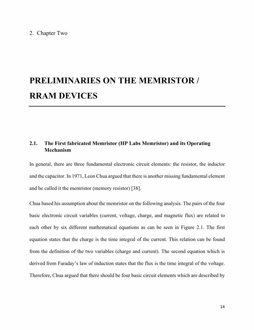
each other by six different mathematical equations as can be seen in Figure 2.1. The first
equation states that the charge is the time integral of the current. This relation can be found
from the definition of the two variables (charge and current). The second equation which is
derived from Faraday’s law of induction states that the flux is the time integral of the voltage.
Therefore, Chua argued that there should be four basic circuit elements which are described by
15
Figure 2.1. The four two-terminal fundamental circuit elements and their related six equations [9].
the remaining four equations between the circuit variable and the memristor is one of these
four elements [9]. These six equations and their related elements are shown in Figure 2.1. In
Figure 2.1, it is clear that the only missing circuit element is the one between the two variables,
the charge and the flux. This missing element is the memristor. The memristor is a two terminal
nonlinear circuit element with a memristance 𝑀 that relates the charge and the flux according
to the following equation:
𝑑𝜑 = 𝑀𝑑𝑞 (1)
where 𝜑 is the magnetic flux and 𝑞 is the electric charge.
The value of M is not constant but a function of the charge q. This results in a nonlinear relation
between the charge and the flux. The I–V characteristic of this nonlinear memristor under
16
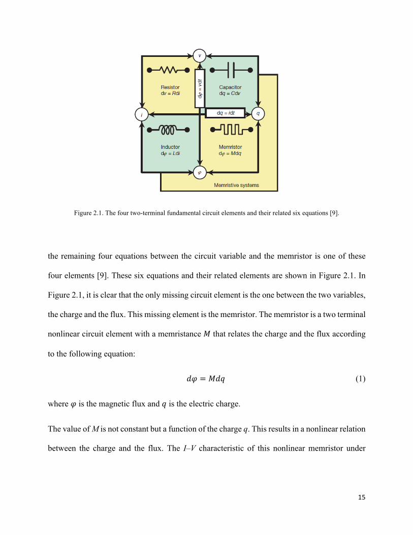
Figure 2.2. (a) The memristor I–V characteristics loops for two different frequencies where the hysteresis loop collapses when the sweep frequency is increased. (b) The memristor applied sinusoidal voltage v0sin(w0t) (in blue) and the resulting current (in green) as a function of time for the memristor device in [9] where v0 is the magnitude of the applied voltage and w0 is the frequency [9].
sinusoidal input signal is similar to Lissajous figures with a frequency dependent property as
shown in Figure 2.2(a). Figure 2.2(a) shows the ideal I–V characteristic loops of the MIM
memristor as reported by HP in [9] for two different frequencies where the hysteresis loop
collapses when the sweep frequency is increased. Figure 2.2(b) shows the applied input signal
to the two terminal memristor device together with the resulted current [9]. However, there is
no combination of any nonlinear basic circuit elements which can reproduce the circuit
behaviour of the memristor. Since the memristor has this nonlinear behaviour, it can be used
in the integrated circuits to provide a unique function such as resistance switching with high
densities devices [9].
17
Until 2008, Chua’s idea about the memristor has not been explored and no physical model has
been fabricated to show the actual operation of the memristor. However, in 2008, a research
group from HP labs announced for the first time that the memristor element exists naturally in
the nanometer scale electronic systems where both the ionic conduction mechanism and the
solid state electronic are used (under external bias) to describe the memristor equations [9].
The first memristor cell structure announced by HP labs consists of two layers of TiO2
sandwiched between two platinum electrodes. A schematic diagram of this memristor is shown
in Figure 2.3. The first layer is highly doped with oxygen vacancies (behave as a
semiconductor) while the second one is an un-doped layer with a higher resistivity (behave as
an insulator layer). In Figure 2.3, D is the total length of the oxide layer and 𝑤 is the length of
the doped region. However, depending on the amount of the electric charge flowing in the cell
(under an external applied stimulus voltage 𝑉), the boundary between the two regions in Figure
2.3 is moving in the same direction of the passing current 𝐼 [9]. This movement is caused by
the oxygen ions/vacancies movement. The flow of mobile dopants increases and decreases the
state variable width 𝑤 of the doped region. Therefore, the resulted memristor total resistance
equals to the sum of the series resistances of the doped and undoped regions and is given by
[9]:
𝑉 = 𝑅GHIJ+ 𝑅GKK 1 − I
J𝐼 (2)
where 𝑅GH and 𝑅GKK are the resistances of the semiconductor layer for the memristor when 𝑤
=1 and 0, respectively.
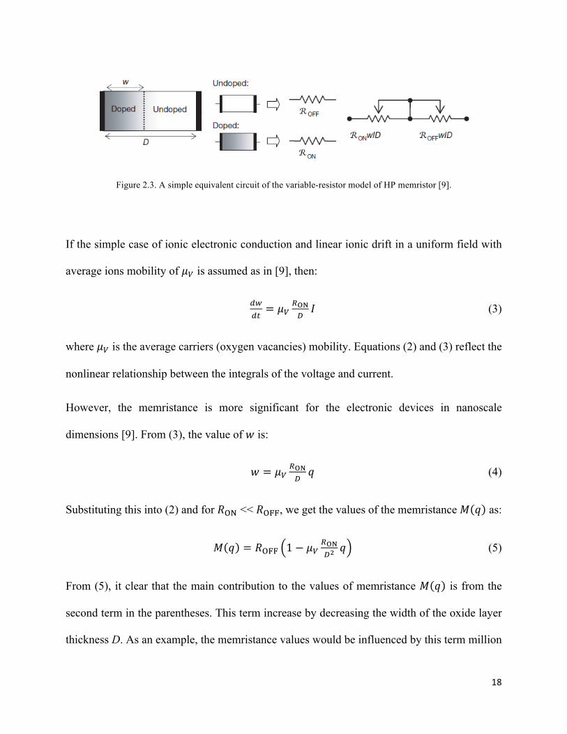
18
Figure 2.3. A simple equivalent circuit of the variable-resistor model of HP memristor [9].
If the simple case of ionic electronic conduction and linear ionic drift in a uniform field with
average ions mobility of 𝜇O is assumed as in [9], then:
PIPQ= 𝜇O
RSTJ𝐼 (3)
where 𝜇O is the average carriers (oxygen vacancies) mobility. Equations (2) and (3) reflect the
nonlinear relationship between the integrals of the voltage and current.
However, the memristance is more significant for the electronic devices in nanoscale
dimensions [9]. From (3), the value of 𝑤 is:
𝑤 = 𝜇ORSTJ𝑞 (4)
Substituting this into (2) and for 𝑅GH << 𝑅GKK, we get the values of the memristance 𝑀 𝑞 as:
𝑀 𝑞 = 𝑅GKK 1 − 𝜇ORSTJU
𝑞 (5)
From (5), it clear that the main contribution to the values of memristance 𝑀 𝑞 is from the
second term in the parentheses. This term increase by decreasing the width of the oxide layer
thickness D. As an example, the memristance values would be influenced by this term million
19
time more significantly when switching from microscale to nanoscale dimensions. This
comparison reflects the fact that the memristor does not have a noticeable effect in the
micrometre scale devices while in nanometre scale it has a much greater influence on the
electronic circuit devices [9]. This is the reason for the memristor being uncovered during the
last three decades. However, in order to understand the RS mechanism of the memristor,
hereafter will be referred to as RRAM devices, it is essential to understand how the RRAM
device is formed prior to the RS mechanism.
2.2. Pre-Resistive Switching Process (Electroforming Process) and the Resistive Switching Mechanism of the MIM RRAM Devices
The metal oxides electrical switching mechanism depends on the coupled motion of the ions
and electrons in the oxide material [39]. This electrical switching behaviour is considered as
one of the first examples of the memristor/RRAM which was predicted by Chua in 1971 [39].
However, the RRAM devices need an irreversible one step (electroforming) process prior to
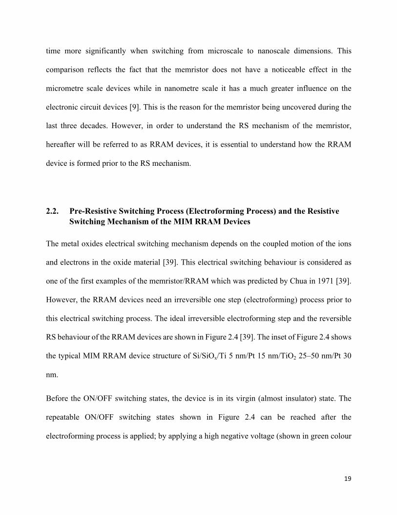
this electrical switching process. The ideal irreversible electroforming step and the reversible
RS behaviour of the RRAM devices are shown in Figure 2.4 [39]. The inset of Figure 2.4 shows
the typical MIM RRAM device structure of Si/SiOx/Ti 5 nm/Pt 15 nm/TiO2 25–50 nm/Pt 30
nm.
Before the ON/OFF switching states, the device is in its virgin (almost insulator) state. The
repeatable ON/OFF switching states shown in Figure 2.4 can be reached after the
electroforming process is applied; by applying a high negative voltage (shown in green colour
20
Figure2.4.The ideal reversible BRS process and the required forming voltage polarity [39].
in Figure 2.4) or high positive voltage (shown in red colour in Figure 2.4). At the
electroforming voltage, the device characteristics will change abruptly to a Higher/Lower
current and Lower/Higher voltage for negative and positive forming voltages, respectively. The
abrupt change in the current indicates the occurrence of the forming and a decrease in the
resistance of the device (several orders in the magnitude). After electroforming process, the
initial switching state depends on the polarity of the voltage of the electroforming state. The
device can then be switched ON and OFF by applying a negative and positive voltages on the
TE, respectively. These switching polarities depend on the asymmetry of the interfaces after
the device fabrication. In the device shown in Figure 2.4, the top interface is Schottky-like
interface while the bottom interface is ohmic [39].
The physics behind the electroforming process can be explained as follows.
21
The electroforming process in insulator oxides changes the conductivity properties of the
insulator (change the behaviour) by applying a high voltage or current (and can be enhanced
by electrical Joule heating effect). This high field results in an electro-reduction process
together with a vacancy creation in the oxide. The oxygen vacancies are formed and then drift
to the cathode (the negatively charged electrode), doping the semiconducting TiO2 oxide to
high conductivities and forming a localized conducting channel through the oxide layer [39].
At the same time, the oxygen ions (O2-) will drift to the anode (the positively charge electrode)
and change into oxygen gas. Subsequent to this one-time step, the device will operate in its RS
(ON/OFF) mode. The oxygen gas formed at the anode could cause a physical deformation in
the junctions which in turn results in large variance in the properties of the final device.
Therefore, it is highly desirable to eliminate the electroforming process completely. This
problem can be reduced by switching the junction area size and the oxide layer thickness into
nanometer scale and controlling the polarity of the electroforming process. Engineering the
device structure can result in an interface controlled electronics switching which replaces the
bulk oxide effect and hence avoid the need for the electroforming process [39].
2.3. The Effect of the Device Area on the Produced Gas Bubbles and The Physical Deformation
The physical deformation problem is related to the area size of the junction of the RRAM
device. In [39], two RRAM samples with 5 µm x 5 µm micro junction and 50 nm x 50 nm nano
junction are formed. The oxide layer TiO2 thickness is the same for both cells, in the range
22
(a) (b)
Figure 2.5. (a) Atomic force micrograph (AFM) image of the 5×5 µm2 RRAM junction before the electroforming process. (b) AFM image of the same the 5×5 µm2 RRAM junction but after applying the electroforming negative voltage. The image shows the bubble formed along the edge of the bottom electrode of the micro scale junction and the pointed tip at the top of this bubble suggests a gap eruption [39].
of 25–50 nm. After the electroforming process, electrical switching performed on them where
all the measurements are done by grounding the bottom electrode (BE) and the voltage is
connected to the top electrode (TE).
No physical deformation appeared in the nano devices whereas in micro devices a clear and
relatively large dome-like appeared beside the edge of the BE. This dome-like deformations is
shown in Figure 2.5(b). It can be seen that on the top of this dome there is an eruption-like
feature. The assumption is that this deformation is the result of the drift of the negatively
charged oxygen ions to the positive electrode. These ions are discharged at that electrode to O2
gas which, after reaching a certain pressure, finds the mechanically weakest point of the film
and erupt from there to form these dome-like phenomena.
As the nano TiO2 films devices are much smaller in linear dimensions and in volume compared
to the micro devices, the amount of the produced material, gas and pressure is much smaller.
23
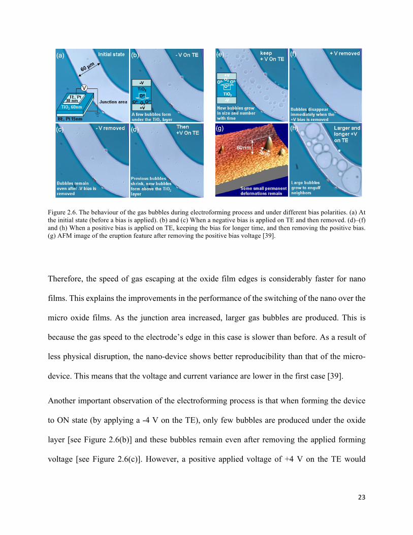
Figure 2.6.The behaviour of the gas bubbles during electroforming process and under different bias polarities. (a) At the initial state (before a bias is applied). (b) and (c) When a negative bias is applied on TE and then removed. (d)–(f) and (h) When a positive bias is applied on TE, keeping the bias for longer time, and then removing the positive bias. (g) AFM image of the eruption feature after removing the positive bias voltage [39].
Therefore, the speed of gas escaping at the oxide film edges is considerably faster for nano
films. This explains the improvements in the performance of the switching of the nano over the
micro oxide films. As the junction area increased, larger gas bubbles are produced. This is
because the gas speed to the electrode’s edge in this case is slower than before. As a result of
less physical disruption, the nano-device shows better reproducibility than that of the micro-
device. This means that the voltage and current variance are lower in the first case [39].
Another important observation of the electroforming process is that when forming the device
to ON state (by applying a -4 V on the TE), only few bubbles are produced under the oxide
layer [see Figure 2.6(b)] and these bubbles remain even after removing the applied forming
voltage [see Figure 2.6(c)]. However, a positive applied voltage of +4 V on the TE would
24
Figure 2.7. Electroforming dependency of the applied bias polarity on the TE (a) Forming the RRAM device into ON state with negative bias. (b) Forming the RRAM device into OFF state with positive bias [39]. The insets in (a) and (b) show the deformation in the RRAM cell after electroforming for both, negative and positive bias polarities, respectively [39].
remove any bubbles under the TiO2 layer and produces more bubbles above this layer and
below the TE layer [see Figure 2.6(d) and (e)]. Increasing the applied voltage would make the
bubbles merge with each other and producing larger bubbles. Once the positive applied voltage
is removed; all the gas bubbles are disappeared in a few seconds [see Figure 2.6(h) and (f)].
These observations are explained as follow [39]: In the first case (negative bias on TE), the
number of gas bubbles is fewer because forming a bubble under the two layers of TiO2 and TE
required more gas pressure than forming the bubbles under only TE layer. Also, the bubbles in
the case of the negative voltage don’t disappear until a positive is applied on the TE which
causes an electrochemical action that reincorporates the gas back to the film. However, in the
case of the bubbles formed above the TiO2 layer (positive bias on TE), they can easily escape
through the edges of the electrodes or through an eruption features through the TE [39].
25
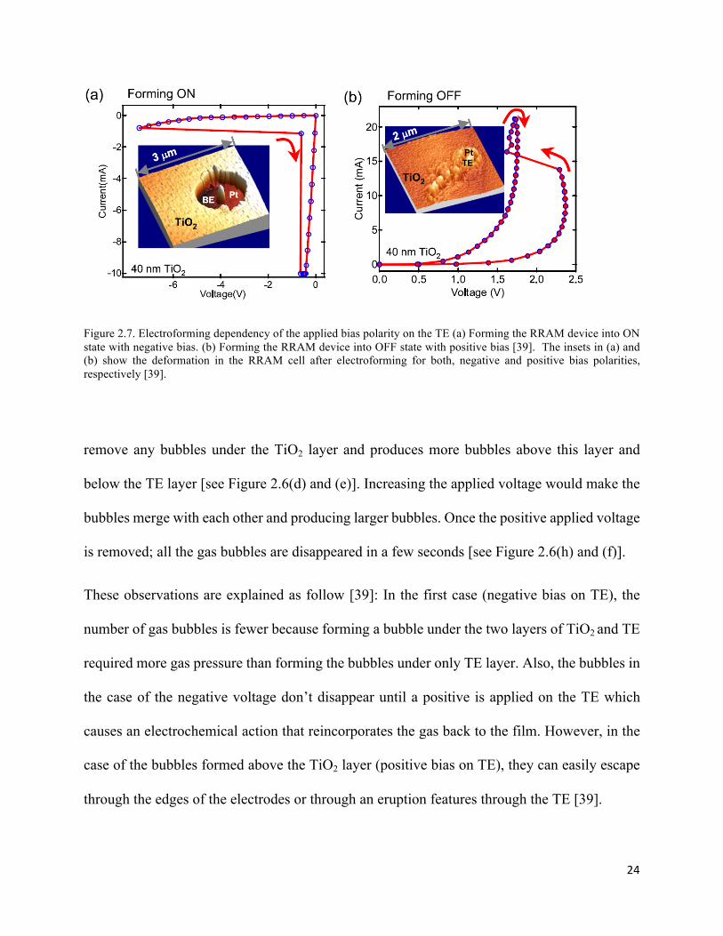
2.4. The Effect of the Asymmetry of the Metal/Oxide interfaces on the Forming Voltage
During the electroforming process, the asymmetry of the two metal/oxide interfaces play a
major role in determining the voltage level (the electric field strength) required for the device
forming. Figure 2.7 [39] shows the MIM RRAM two devices (with 40 nm TiO2) are being
formed by a negative bias [Figure 2.7(a)] and positive bias [Figure 2.7(b)] to reach the ON and
OFF final states, respectively. It can be seen that the average electric field required to form the
device to OFF state (+2.3 V) is much smaller (a round one third) compared to the electric field
required to form the device to the ON state (-7.8 V) [39]. This can be explained by knowing
that the Schottky-like interface between the TE and the oxide TiO2 layer is forward biased
during the forming/switching to the OFF state (positive bias on the TE). Therefore, the current
is higher during this switching stage compared to forming/switching the device to ON state
with a negative bias (reversed biased Schottky barrier). Hence, the possibility of Joule heating
effect is high (the temperature can reach several hundred degrees in this case [39]). Due to the
high temperature, oxygen vacancies mobility can increase by around seven order of magnitude
at 240 0C compared to the mobility at room temperature [39]. This shows that the
electroforming process is first triggered by the applied electric field and then enhanced by the
electrical heating (the oxygen ions/vacancies are created at the region of the high electric field
and then drift into the positive/negative electrode [39]).
26
2.5. Overall Summary of the Electroforming Step
2.5.1. Electroforming the RRAM Device into ON Initial State
1- Electroforming by negative voltage on the TE results in an initial ON state (SET).
2- During SET electroforming, the negative voltage on TE results in a large voltage drop
on the reverse-biased Schottky-like interface. The oxygen vacancies will be generated
at the interface region and stay there until their doping effect reduces the electronic
barrier into conductive and the electric field at that area will drop [39].
3- The current increases but will be limited the by insulating bulk layer which is considered
now as the high electric field region of the RRAM device [39].
4- As more oxygen vacancies are created and drift across the bulk layer to create a CF, the
resistive Schottky-like interface and the resistive bulk layer will both be penetrated by
conducting channel and the RRAM device reach its LRS (ON state).
5- The inset of Figure 2.7(a) shows the device after removing the TE. It can be seen that a
round hole is formed in the oxide layer, indicating that the oxygen gas bubbles are likely
formed under the oxide layer.
2.5.2. Electroforming the RRAM Device into OFF Initial State
1- Electroforming by positive voltage on the TE results in an initial OFF state (RESET).
2- During this stage, the forward-biased Schottky-like interface will be relatively
conductive. Hence, the voltage drop will be concentrated on the bulk layer [39].
27
3- Oxygen ions will drift toward TE and discharge there to form oxygen gas on the top of
the oxide layer and below TE. At the same time, oxygen vacancies will drift away from
the top interface, toward BE which form CF through the oxide film [39].
4- However, due to the polarity of the electric field in this case (positive voltage on TE),
the electric field will repel away the vacancy channels from touching the TE and hence,
Schottky-like interface will not be heavily doped by the oxygen vacancies and the initial
state after forming is OFF state. According to [39], the CF penetrates the bulk layer but
it doesn’t do the same at Schottky-like interface region.
5- The inset of Figure 2.7(b) shows that the oxide layer is less physically deformed by the
produced gas bubbles when compared to electroforming by negative bias (because the
gas bubbles were formed on top of the oxide layer and under TE). The deformation has
mainly affected the TE/oxide layer interface.
6- According to [39], the bubbles are formed in the centre of the junction area and the
position of the conducting channels is adjacent to the bubble area.
28
3. Chapter Three: Literature Review on the MIM and MISM RRAM Models
LITERATURE REVIEW ON THE MIM AND
MISM RRAM MODELS
Summary
Several RRAM models have been presented in the literatures. These models can be divided
into MIM RRAM models and MISM (bi-layered) RRAM models. In this chapter, a literature
review on both types of RRAM models will be conducted to further explain why the available
models cannot be used directly to reproduce the behaviour of the Ta2O5/TaOx bi-layered
RRAM devices.
3.1. MIM Mathematical and SPICE RRAM Models
From the literature, it can be seen that a great progress has been made on the analytical and
SPICE modelling of the MIM RRAM devices [15], [40], [41], [42], [43]. Also, evaluation
criteria have been introduced in [44] which can be used to check the applicability of these
models to simulate the RS behaviour.
29
Some models aim to have the flexibility to fit into different physical MIM RRAM models [15],
[40]. The model in [40] is correlated against several MIM RRAM devices with an average error
of 6.04%. It was also tested in a relatively large circuit of 256 RRAM devices and showed
better results when compared to the available MIM RRAM devices (caused less convergence
errors). In this model, a hyperbolic sinusoid equation of the MIM tunnel barrier for electron
tunnelling is used to model the MIM junction conduction which showed the best fit with the
experimental data. However, in the Ta2O5/TaOx bi-layered RRAM, the conduction equation is
based on Schottky barrier modulation and tunnelling mechanism in the MIS structure. The
model in [40] uses fitting parameters to show that the RRAM is more conductive in the positive
region than the negative region whereas the Ta2O5/TaOx bi-layered RRAM exhibit this
behaviour due to its Schottky barrier being forward biased and reversed biased for positive and
negative bias, respectively, which should be taken into account when developing a Ta2O5/TaOx
bi-layered RRAM model.
The state variable in [40] is based on two mathematical functions: the first function accounts
for the threshold voltage required for the state change. This function uses fitting parameters to
determine how quickly the state change once the threshold voltage is reached. Although this
function can provide different threshold voltages based on the bias polarity, it doesn’t reflect
the physics involved in the Ta2O5/TaOx bi-layered RRAM devices. The state variable in [40]
does not take into consideration the ions hopping mechanisms in the Ta2O5/TaOx bi-layered
RRAM which is the responsible mechanism for the change in the resistance during the RS
process and can be modelled using the ions hopping hyperbolic sinusoidal programming
30
Figure 3.1. The simulation results of the RRAM physical devices in (a) [45], (b) [46], (c) [47] and [48], and (d) [49] modelled using the MIM RRAM model proposed in [40].
threshold (Mott and Gurney rigid point-ion model) and Joule heating effect. It also does not
consider the electric field effect in the ions hopping region which determines the threshold
voltage and should be incorporated in the bi-layered RRAM mathematical model. The second
function in [40] models the nonlinear dopant drift based on the bias polarity.
Figure 3.1(a)–(d) shows the MIM RRAM devices in [45], [46], [47], [48], and [49] modelled
using the MIM RRAM model in [40]. The simulation results in Figure 3.1(a) match with the
experimental data in [45] with an average error of 6.64%. Figure 3.1(b) shows the simulation
results of the RRAM device in [46], modelled using the RRAM SPICE model in [40] with an
average error of 6.21%. Figure 3.1(c) shows the simulated I–V curves from the RRAM devices
in [47] and [48] which matches to the experimental data with an average error of 5.97%. As a
31
final example for using the SPICE model in [40] to model MIM RRAM devices, Figure 3.1(d)
depicts the simulation results of modelling the physical RRAM device in [49] with an average
error of 6.15%. Although the MIM RRAM model in [40] showed good agreements with the
experimental results for different MIM RRAM devices, it can be seen in Figure 3.1 that all
these RRAM devices showed different characteristics when compared to the Ta2O5/TaOx bi-
layered RRAM. Hence, the SPICE model in [40] cannot be applied directly to the Ta2O5/TaOx
bi-layered RRAM.
Another MIM RRAM model is presented in [15] and proved that it can fit into several MIM
RRAM devices with reasonable accuracy, computational efficiency, and with mean error of
0.2%. The I–V relationship in this model is not defined and claimed that it can be chosen from
any of the available I–V conduction relationships. The expression of the derivative of the state
variable of the model in [15] (which also represents the RS speed) is claimed to have the
flexibility to fit into any RRAM device type. However, this expression does not take the
intrinsic Schottky-like interface, Joule heating effect, ions hopping mechanism and the electric
field dependence of the growth rate equation into consideration. Therefore, similar to the model
in [40], this model cannot be applied directly to the Ta2O5/TaOx bi-layered RRAM devices
which exhibit different characteristics when compared to the model in [15].
Some models have been proposed to model the TaOx-based MIM and bi-layered RRAM
devices as in [41]. In [41], a circuit-based model for TaOx-based MIM RRAM RS is presented
and implemented in VerilogA. The model is designed to match the behaviour of Pt/TaOx/Ta
MIM RRAM device with the TaOx thickness of 11 nm and the obtained simulation results were
32
Figure 3.2. The Equivalent circuit model and the cell structure of the Pt/TaOx/Ta MIM RRAM model in [41].
compared to the experimental results taken from [50]. This model is one of the best physical-
oriented TaOx-based RRAM models which takes into consideration Schottky-like interface
between the TE and the oxide layer. It also considers the temperature effect during RS.
Furthermore, this model also added the ionic current and the areal current components and used
the oxygen vacancies concentration as the state variable which can change the value of the
electronic resistance Re1 and Schottky barrier height (see Figure 3.2). As can be seen in Figure
3.2, the model consists of a well conducting plug (modelled as a series resistor) and a more
resistive switching layer (the disc in Figure 3.2).
However, due to the device thickness (11 nm) in [41], a large area dependent parallel current
is presented in the device besides the current through the CF (see Figure 3.2). This areal current
33
Figure 3.3. The measured I–V characteristics from [50] and the simulation results in [41] for the Pt/TaOx/Ta MIM RRAM device with TaOx thickness of 11 nm plotted on logarithmic scale [41].
is the dominant current during HRS. For this areal current, Poole-Frenkel-type conduction
mechanism showed good fitting for the 11 nm TaOx-based MIM RRAM. Besides that, Fowler-
Nordheim tunnelling mechanism showed good fitting when used for the negative bias.
However, it is expected that the current of the RRAM devices has a great relevance for the
oxide thickness (especially at HRS) which implies that different conduction mechanisms exist
for RRAM devices with different oxide thickness [32], [50]. For example, Shcottky barrier
modulation and tunnelling mechanism showed good fitting for the Ta2O5/TaOx bi-layered
RRAM with switching layer thickness in the range of 3–4 nm while the conduction mechanism
used in [41] (Poole-Frenkel-type conduction and Fowler-Nordheim tunnelling mechanism) did
not fit into the same RRAM with oxide thickness 3–4 nm. This behaviour agrees with the
physics of these conduction mechanisms, where each current mechanism is valid under certain
range of thicknesses only. Therefore, the model in [41] is limited to the devices with a relatively
thick oxide layers and cannot be applied directly or modified to fit the Ta2O5/TaOx bi-layered
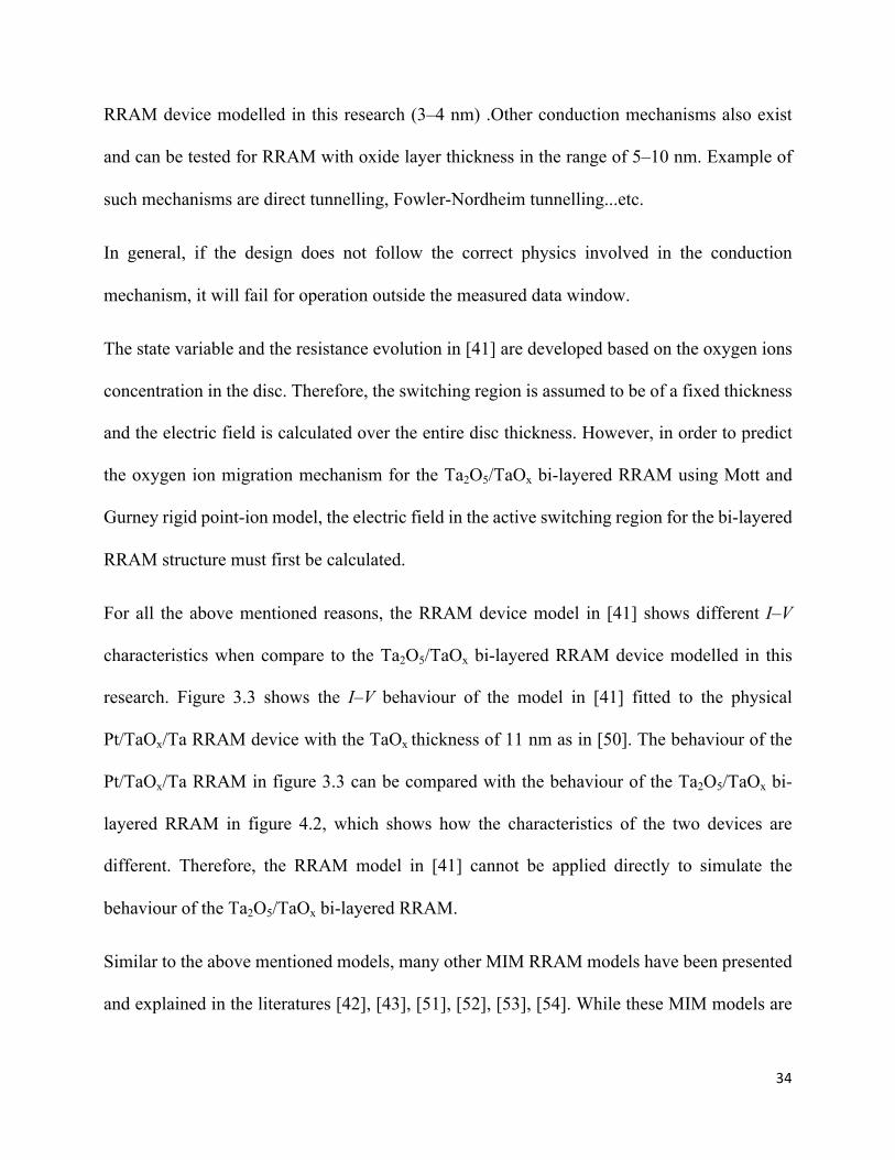
34
RRAM device modelled in this research (3–4 nm) .Other conduction mechanisms also exist
and can be tested for RRAM with oxide layer thickness in the range of 5–10 nm. Example of
such mechanisms are direct tunnelling, Fowler-Nordheim tunnelling...etc.
In general, if the design does not follow the correct physics involved in the conduction
mechanism, it will fail for operation outside the measured data window.
The state variable and the resistance evolution in [41] are developed based on the oxygen ions
concentration in the disc. Therefore, the switching region is assumed to be of a fixed thickness
and the electric field is calculated over the entire disc thickness. However, in order to predict
the oxygen ion migration mechanism for the Ta2O5/TaOx bi-layered RRAM using Mott and
Gurney rigid point-ion model, the electric field in the active switching region for the bi-layered
RRAM structure must first be calculated.
For all the above mentioned reasons, the RRAM device model in [41] shows different I–V
characteristics when compare to the Ta2O5/TaOx bi-layered RRAM device modelled in this
research. Figure 3.3 shows the I–V behaviour of the model in [41] fitted to the physical
Pt/TaOx/Ta RRAM device with the TaOx thickness of 11 nm as in [50]. The behaviour of the
Pt/TaOx/Ta RRAM in figure 3.3 can be compared with the behaviour of the Ta2O5/TaOx bi-
layered RRAM in figure 4.2, which shows how the characteristics of the two devices are
different. Therefore, the RRAM model in [41] cannot be applied directly to simulate the
behaviour of the Ta2O5/TaOx bi-layered RRAM.
Similar to the above mentioned models, many other MIM RRAM models have been presented
and explained in the literatures [42], [43], [51], [52], [53], [54]. While these MIM models are
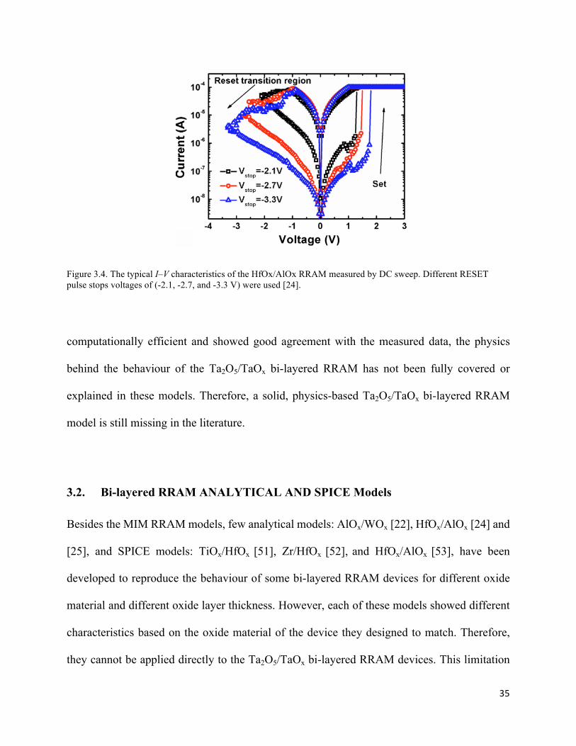
35
Figure 3.4. The typical I–V characteristics of the HfOx/AlOx RRAM measured by DC sweep. Different RESET pulse stops voltages of (-2.1, -2.7, and -3.3 V) were used [24].
computationally efficient and showed good agreement with the measured data, the physics
behind the behaviour of the Ta2O5/TaOx bi-layered RRAM has not been fully covered or
explained in these models. Therefore, a solid, physics-based Ta2O5/TaOx bi-layered RRAM
model is still missing in the literature.
3.2. Bi-layered RRAM ANALYTICAL AND SPICE Models
Besides the MIM RRAM models, few analytical models: AlOx/WOx [22], HfOx/AlOx [24] and
[25], and SPICE models: TiOx/HfOx [51], Zr/HfOx [52], and HfOx/AlOx [53], have been
developed to reproduce the behaviour of some bi-layered RRAM devices for different oxide
material and different oxide layer thickness. However, each of these models showed different
characteristics based on the oxide material of the device they designed to match. Therefore,
they cannot be applied directly to the Ta2O5/TaOx bi-layered RRAM devices. This limitation
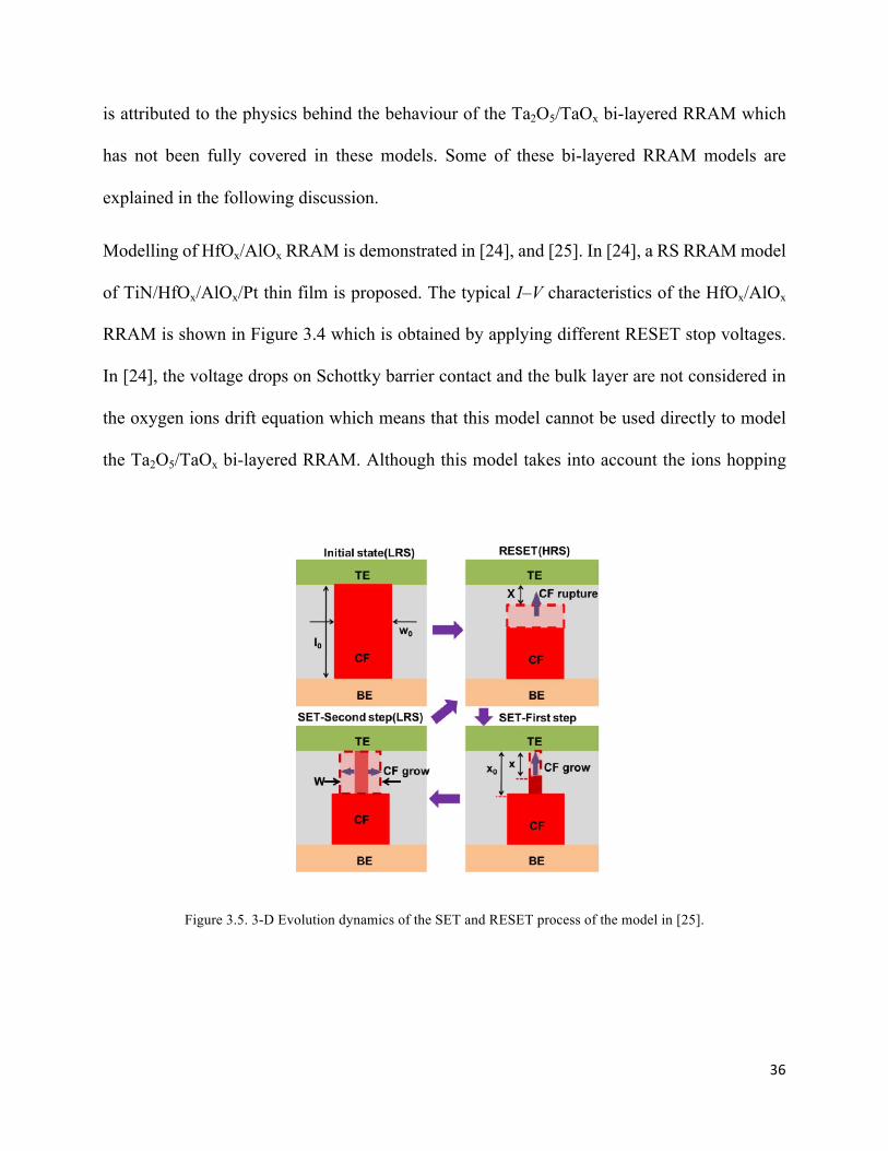
36
is attributed to the physics behind the behaviour of the Ta2O5/TaOx bi-layered RRAM which
has not been fully covered in these models. Some of these bi-layered RRAM models are
explained in the following discussion.
Modelling of HfOx/AlOx RRAM is demonstrated in [24], and [25]. In [24], a RS RRAM model
of TiN/HfOx/AlOx/Pt thin film is proposed. The typical I–V characteristics of the HfOx/AlOx
RRAM is shown in Figure 3.4 which is obtained by applying different RESET stop voltages.
In [24], the voltage drops on Schottky barrier contact and the bulk layer are not considered in
the oxygen ions drift equation which means that this model cannot be used directly to model
the Ta2O5/TaOx bi-layered RRAM. Although this model takes into account the ions hopping
Figure 3.5. 3-D Evolution dynamics of the SET and RESET process of the model in [25].
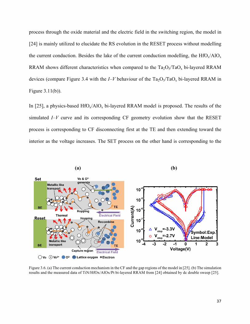
37
process through the oxide material and the electric field in the switching region, the model in
[24] is mainly utilized to elucidate the RS evolution in the RESET process without modelling
the current conduction. Besides the lake of the current conduction modelling, the HfOx/AlOx
RRAM shows different characteristics when compared to the Ta2O5/TaOx bi-layered RRAM
devices (compare Figure 3.4 with the I–V behaviour of the Ta2O5/TaOx bi-layered RRAM in
Figure 3.11(b)).
In [25], a physics-based HfOx/AlOx bi-layered RRAM model is proposed. The results of the
simulated I–V curve and its corresponding CF geometry evolution show that the RESET
process is corresponding to CF disconnecting first at the TE and then extending toward the
interior as the voltage increases. The SET process on the other hand is corresponding to the
(a) (b)
Figure 3.6. (a) The current conduction mechanism in the CF and the gap regions of the model in [25]. (b) The simulation results and the measured data of TiN/HfOx/AlOx/Pt bi-layered RRAM from [24] obtained by dc double sweep [25].
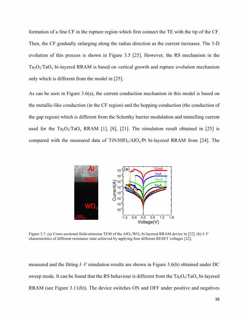
38
formation of a fine CF in the rupture region which first connect the TE with the tip of the CF.
Then, the CF gradually enlarging along the radius direction as the current increases. The 3-D
evolution of this process is shown in Figure 3.5 [25]. However, the RS mechanism in the
Ta2O5/TaOx bi-layered RRAM is based on vertical growth and rupture evolution mechanism
only which is different from the model in [25].
As can be seen in Figure 3.6(a), the current conduction mechanism in this model is based on
the metallic-like conduction (in the CF region) and the hopping conduction (the conduction of
the gap region) which is different from the Schottky barrier modulation and tunnelling current
used for the Ta2O5/TaOx RRAM [1], [8], [21]. The simulation result obtained in [25] is
compared with the measured data of TiN/HfOx/AlOx/Pt bi-layered RRAM from [24]. The
Figure 3.7. (a) Cross-sectional field-emission TEM of the AlOx/WOx bi-layered RRAM device in [22]. (b) I–V characteristics of different resistance state achieved by applying four different RESET voltages [22].
measured and the fitting I–V simulation results are shown in Figure 3.6(b) obtained under DC
sweep mode. It can be found that the RS behaviour is different from the Ta2O5/TaOx bi-layered
RRAM (see Figure 3.11(b)). The device switches ON and OFF under positive and negatives
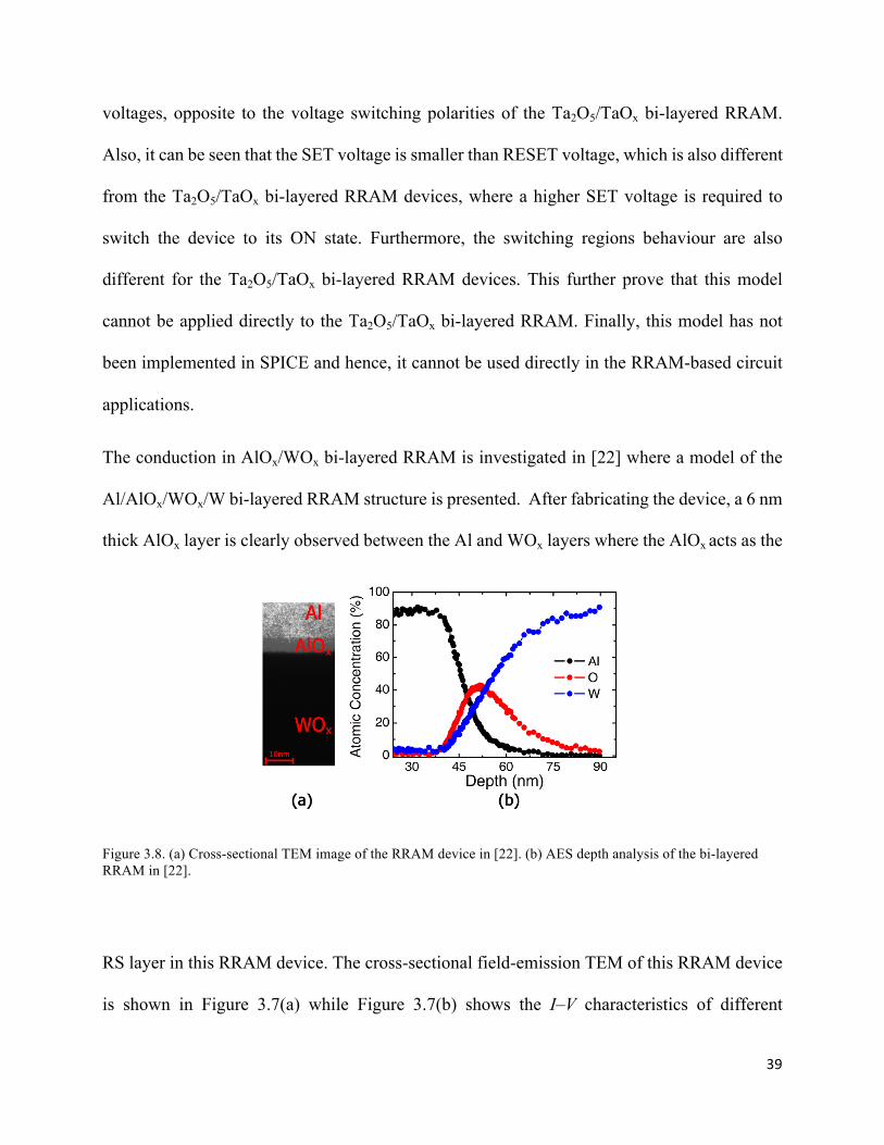
39
voltages, opposite to the voltage switching polarities of the Ta2O5/TaOx bi-layered RRAM.
Also, it can be seen that the SET voltage is smaller than RESET voltage, which is also different
from the Ta2O5/TaOx bi-layered RRAM devices, where a higher SET voltage is required to
switch the device to its ON state. Furthermore, the switching regions behaviour are also
different for the Ta2O5/TaOx bi-layered RRAM devices. This further prove that this model
cannot be applied directly to the Ta2O5/TaOx bi-layered RRAM. Finally, this model has not
been implemented in SPICE and hence, it cannot be used directly in the RRAM-based circuit
applications.
The conduction in AlOx/WOx bi-layered RRAM is investigated in [22] where a model of the
Al/AlOx/WOx/W bi-layered RRAM structure is presented. After fabricating the device, a 6 nm
thick AlOx layer is clearly observed between the Al and WOx layers where the AlOx acts as the
Figure 3.8. (a) Cross-sectional TEM image of the RRAM device in [22]. (b) AES depth analysis of the bi-layered RRAM in [22].
RS layer in this RRAM device. The cross-sectional field-emission TEM of this RRAM device
is shown in Figure 3.7(a) while Figure 3.7(b) shows the I–V characteristics of different
40
resistance state achieved by applying four different RESET voltages. The first imperative
remark that can be observed in Figure 3.7 is that the device shows opposite switching polarity
when compared to the Ta2O5/TaOx bi-layered RRAM where SET process occurs when a
positive bias is applied on the TE. This behaviour can be explained as follows.
Figure 3.8(b) shows the AES depth analysis which confirms the existence of W, Al, and O
elements in the AlOx switching layer. This means that this layer could have AlOx, WOx (oxygen
could form bonds with either Al or W atoms), and free Al and W metals. However, during SET
process, the metal-O bonds break and then the oxygen ions diffuse to the top Al electrode (due
to the effect of the electric field) [22], which leave metal atoms in the interface layer. The metal
atoms form metal CF. According to [22], it is expected that it is easier for the oxygen to break
away from W-O bond than from Al-O bonds in the AlOx layer. This is because the W-O bond
is much weaker than Al-O bond (Gibbs energies are -506.63 kJ/mol and -1582.3 kJ/mol for W-
O and Al-O bonds, respectively). As a result, W contributes more to the metal filament than
Al. However, the RS process in the Ta2O5/TaOx bi-layered RRAM is different, where the CF
is formed due to oxygen ions hopping and the doping effect of their corresponding oxygen
vacancies, not due to the metal atoms as in the AlOx/WOx bi-layered RRAM.
The current conduction mechanism in [22] at HRS is assumed to follow Schottky emission at
the Al- AlOx interface which showed good fitting with the experimental data. The conduction
mechanism at LRS is assumed to be ohmic conduction while the conduction between LRS and
HRS (medium resistance) is assumed to be electron hopping conduction mechanism. However,
Schottky emission model in [22] is different from that in Ta2O5/TaOx bi-layered RRAM [21].
It does not take into account the possible tunnelling, the effect of the continuous variation of
the interface traps, and the image force lowering [32]. The image force is an induced charge on
41
the metal electrode surface due to the presence of an electron/hole on the semiconductor
interface. This charge is equal to the carrier charge at the semiconductor but with opposite
polarity. This leads to the formation of an attraction force between the carrier charge and its
image charge, inducing a potential energy on the carriers. The potential associated with the
charge carriers together with the potential energy due to the applied field reduce the effective
Schottky barrier height [32]. The difference in the conduction mechanism could be attributed
to the thicker switching layer in the model in [22] (6 nm) when compared to that of the
Ta2O5/TaOx RRAM (3 and 4 nm) [32], [50]. It can also be attributed to the difference in the
switching interface material (Al-AlOx for the model in [22] and Pt-Ta2O5 for the model in this
research). In addition to the difference in the conduction mechanism, the model [22] does not
model the RS dynamic behaviour.
In addition to these bi-layered RRAM models, several analytical and physical Ta2O5/TaOx bi-
layered RRAM models have been illustrated in the literature [1], [8], [16], [17], [18], [19], [20],
[21], and some of these models have been explained in [21]. However, to the best of the
researcher knowledge, these models have not been automated through a computer aided design
tool and the SPICE model to predict the Ta2O5/TaOx bi-layered RRAM device behaviour in the
circuit level is not yet available.
In [18], an electro-thermal RS model for the Ta2O5/TaOx bi-layered RRAM is presented. The
model is based on the temperature and field accelerated migration of oxygen vacancies. The
model predicts the temperature inside the doped region and it is one of the best models that
investigate the thermal effect of the oxygen ions during RS in the Ta2O5/TaOx RRAM. The RS
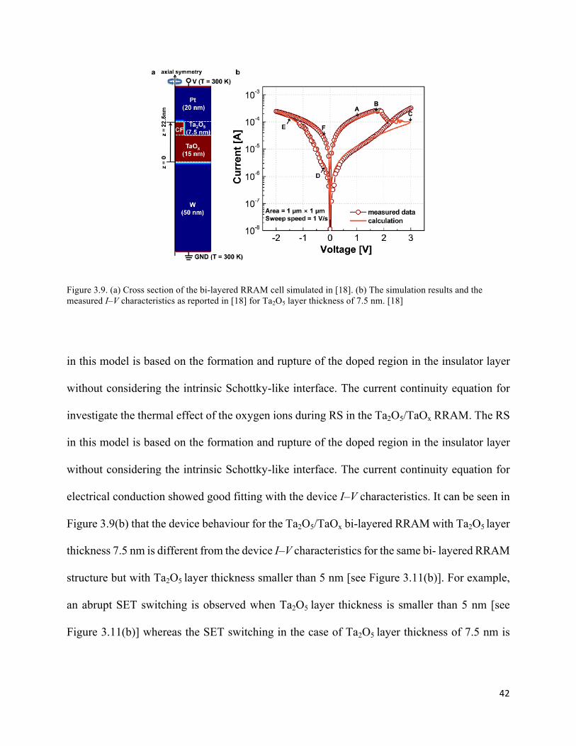
42
Figure 3.9. (a) Cross section of the bi-layered RRAM cell simulated in [18]. (b) The simulation results and the measured I–V characteristics as reported in [18] for Ta2O5 layer thickness of 7.5 nm. [18]
in this model is based on the formation and rupture of the doped region in the insulator layer
without considering the intrinsic Schottky-like interface. The current continuity equation for
investigate the thermal effect of the oxygen ions during RS in the Ta2O5/TaOx RRAM. The RS
in this model is based on the formation and rupture of the doped region in the insulator layer
without considering the intrinsic Schottky-like interface. The current continuity equation for
electrical conduction showed good fitting with the device I–V characteristics. It can be seen in
Figure 3.9(b) that the device behaviour for the Ta2O5/TaOx bi-layered RRAM with Ta2O5 layer
thickness 7.5 nm is different from the device I–V characteristics for the same bi- layered RRAM
structure but with Ta2O5 layer thickness smaller than 5 nm [see Figure 3.11(b)]. For example,
an abrupt SET switching is observed when Ta2O5 layer thickness is smaller than 5 nm [see
Figure 3.11(b)] whereas the SET switching in the case of Ta2O5 layer thickness of 7.5 nm is
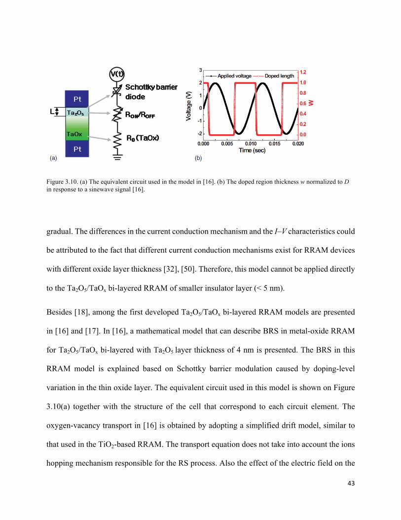
43
Figure 3.10. (a) The equivalent circuit used in the model in [16]. (b) The doped region thickness w normalized to D in response to a sinewave signal [16].
gradual. The differences in the current conduction mechanism and the I–V characteristics could
be attributed to the fact that different current conduction mechanisms exist for RRAM devices
with different oxide layer thickness [32], [50]. Therefore, this model cannot be applied directly
to the Ta2O5/TaOx bi-layered RRAM of smaller insulator layer (< 5 nm).
Besides [18], among the first developed Ta2O5/TaOx bi-layered RRAM models are presented
in [16] and [17]. In [16], a mathematical model that can describe BRS in metal-oxide RRAM
for Ta2O5/TaOx bi-layered with Ta2O5 layer thickness of 4 nm is presented. The BRS in this
RRAM model is explained based on Schottky barrier modulation caused by doping-level
variation in the thin oxide layer. The equivalent circuit used in this model is shown on Figure
3.10(a) together with the structure of the cell that correspond to each circuit element. The
oxygen-vacancy transport in [16] is obtained by adopting a simplified drift model, similar to
that used in the TiO2-based RRAM. The transport equation does not take into account the ions
hopping mechanism responsible for the RS process. Also the effect of the electric field on the
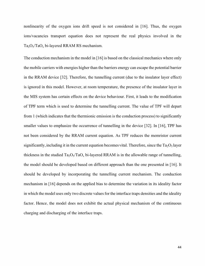
44
nonlinearity of the oxygen ions drift speed is not considered in [16]. Thus, the oxygen
ions/vacancies transport equation does not represent the real physics involved in the
Ta2O5/TaOx bi-layered RRAM RS mechanism.
The conduction mechanism in the model in [16] is based on the classical mechanics where only
the mobile carriers with energies higher than the barriers energy can escape the potential barrier
in the RRAM device [32]. Therefore, the tunnelling current (due to the insulator layer effect)
is ignored in this model. However, at room temperature, the presence of the insulator layer in
the MIS system has certain effects on the device behaviour. First, it leads to the modification
of TPF term which is used to determine the tunnelling current. The value of TPF will depart
from 1 (which indicates that the thermionic emission is the conduction process) to significantly
smaller values to emphasize the occurrence of tunnelling in the device [32]. In [16], TPF has
not been considered by the RRAM current equation. As TPF reduces the memristor current
significantly, including it in the current equation becomes vital. Therefore, since the Ta2O5 layer
thickness in the studied Ta2O5/TaOx bi-layered RRAM is in the allowable range of tunnelling,
the model should be developed based on different approach than the one presented in [16]. It
should be developed by incorporating the tunnelling current mechanism. The conduction
mechanism in [16] depends on the applied bias to determine the variation in its ideality factor
in which the model uses only two discrete values for the interface traps densities and the ideality
factor. Hence, the model does not exhibit the actual physical mechanism of the continuous
charging and discharging of the interface traps.
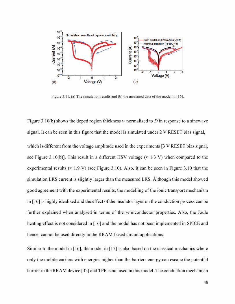
45
Figure 3.11. (a) The simulation results and (b) the measured data of the model in [16].
Figure 3.10(b) shows the doped region thickness w normalized to D in response to a sinewave
signal. It can be seen in this figure that the model is simulated under 2 V RESET bias signal,
which is different from the voltage amplitude used in the experiments [3 V RESET bias signal,
see Figure 3.10(b)]. This result in a different HSV voltage (≈ 1.3 V) when compared to the
experimental results (≈ 1.9 V) (see Figure 3.10). Also, it can be seen in Figure 3.10 that the
simulation LRS current is slightly larger than the measured LRS. Although this model showed
good agreement with the experimental results, the modelling of the ionic transport mechanism
in [16] is highly idealized and the effect of the insulator layer on the conduction process can be
further explained when analysed in terms of the semiconductor properties. Also, the Joule
heating effect is not considered in [16] and the model has not been implemented in SPICE and
hence, cannot be used directly in the RRAM-based circuit applications.
Similar to the model in [16], the model in [17] is also based on the classical mechanics where
only the mobile carriers with energies higher than the barriers energy can escape the potential
barrier in the RRAM device [32] and TPF is not used in this model. The conduction mechanism
46
in [17] is using a constant ideality factor. Hence, similar to the RRAM model in [16], the model
does not exhibit the actual physical mechanism of the continuous charging and discharging of
the interface traps. In addition, Joule heating effect is not considered during the RS process in
[17] and the temperature is assumed to be at room temperature. Although the model in [17]
showed good agreement with the experimental results, the modelling of the effect of the
insulator layer on the conduction process can be further explained when analysed in terms of
the semiconductor properties. Most importantly, this model has not been implemented as
SPICE subcircuit. Therefore, it cannot be used in RRAM-based circuit applications.
47
4. Chapter Four: Mathematical Modelling of the Pt/Ta2O5/TaOx/Pt Bi-Layered RRAM
MATHEMATICAL MODELING OF THE
Pt/Ta2O5/TaOX/Pt BI-LAYERED RRAM
Related Publications: F. O. Hatem, P. W. C. Ho, T. N. Kumar, and H. A. F. Almurib, “Modeling of bipolar resistive switching of a nonlinear MISM memristor,” Semicond. Sci. Technol., vol. 30, no. 11, 2015.
Related Awards: ThisjournalarticlehasbeenselectedbyIOPPublishingEditorialBoardasoneofthe"SemiconductorScienceandTechnology"Highlightsof2015.
Links to this award: http://iopscience.iop.org/0268-1242/page/Highlights-of-2015 https://blogs.nottingham.ac.uk/malaysiaknowledgetransfer/2016/06/21/66762/
48
Summary
This chapter presents a deep theoretical discussion of the Ta2O5/TaOx bi-layered RRAM and
propose a novel and accurate mathematical model of a BRS of the bi-layered Pt/Ta2O5/TaOx/Pt
RRAM. The proposed model describes the BRS behaviour based on the fundamentals and
physical characteristics of the MIS system. It also includes the physical characteristics of the
insulator layer. When compared to the existing models with the same cell structure, the novelty
of the proposed model lies in incorporating TPF term between the semiconductor and the metal
layers and therefore, demonstrating its effect on the conduction mechanism. In addition, the
effect of continuous variation of the interface traps densities and the ideality factor during BRS
is explained and modelled using the semiconductor properties and the characteristics of the
MIS system. Thus, the model emphasizes the dependency of the RRAM current on the physical
characteristics of the insulator layer. This overcomes the previous assumption that the interface
traps in the MISM RRAM are fixed during the switching time and only changes once the
polarity of the RRAM input signal is changed. Moreover, the electric field equation for the
active region is derived for the bi-layered RRAM structure which is used together with Mott
and Gurney rigid point-ion model and Joule heating effect to model the oxygen ion migration
mechanism. Finally, the model also demonstrates the self-limiting growth of the doped region.
The modelling steps are introduced in details throughout the chapter sections and the final
model is correlated against the experimental results of the published devices which have the
same bi-layered RRAM structure and same material. Extensive simulation is carried out on the
proposed model which show that the proposed model is in good agreement with the physical
characteristics of the Pt/Ta2O5/TaOx/Pt RRAM.
49
4.1. The Structure and the Semiconductor Properties of the Pt/Ta2O5/TaOx/Pt RRAM Proposed Model
4.1.1. The Structure of the Proposed Model
The structure of the oxide-based Pt/Ta2O5/TaOx/Pt RRAM cell modelled in this chapter is
shown in Figure 4.1, which consists of a high resistivity oxide layer (top layer) fixed on a metal-
rich less resistive layer (base layer) sandwiched between two metal electrodes. The TaOx layer
is highly doped with oxygen vacancies (𝑉V) which behave like n-type semiconductor and its
resistance is assumed to be 𝑅X. This resistance is assumed to be constant during the whole
switching cycles. 𝐷 is the thickness of the Ta2O5 layer and its resistance 𝑅Y. The resistance of
the Ta2O5 oxide layer is variable due to the drifting of oxygen vacancies in and out of the layer
during the RS mechanism. The thickness of these layers varies from 2-5 nm and 10-50 nm for
the top and base layers, respectively [17]. In this chapter, the thickness of the insulating layer
Ta2O5 is 4-nm which can be changed to fit the different available bi-layered RRAM models of
the same structure. The term 𝑤 is used to refer to the length of the un-doped region in the CF.
The doped region is the CF region with high concentration of donor-like oxygen vacancies (the
low resistance region of the CF). Similar to the previous work [1], [16] the Pt BE will be
grounded and all the applied voltages and simulation measurements will take place on the TE
which is an independent metal layer that is unaffected by the switching mechanism [30].
4.1.2. The Bipolar Resistive Switching Mechanism of the Proposed Model
Low Resistance State: LRS is reached when a negative voltage is applied as in Figure 4.1(a).
In this case, oxygen ions in the Ta2O5 layer and in the vicinity of the interface region will be
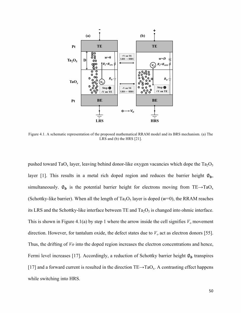
50
Figure 4.1. A schematic representation of the proposed mathematical RRAM model and its BRS mechanism. (a) The LRS and (b) the HRS [21].
pushed toward TaOx layer, leaving behind donor-like oxygen vacancies which dope the Ta2O5
layer [1]. This results in a metal rich doped region and reduces the barrier height ∅𝒃,
simultaneously. ∅𝒃 is the potential barrier height for electrons moving from TE→TaOx
(Schottky-like barrier). When all the length of Ta2O5 layer is doped (𝑤=0), the RRAM reaches
its LRS and the Schottky-like interface between TE and Ta2O5 is changed into ohmic interface.
This is shown in Figure 4.1(a) by step 1 where the arrow inside the cell signifies Vo movement
direction. However, for tantalum oxide, the defect states due to Vo act as electron donors [55].
Thus, the drifting of Vo into the doped region increases the electron concentrations and hence,
Fermi level increases [17]. Accordingly, a reduction of Schottky barrier height ∅𝒃 transpires
[17] and a forward current is resulted in the direction TE→TaOx. A contrasting effect happens
while switching into HRS.
Pt
Pt
Ta2O5
TaOx
BE
TE
+
D𝒘=0
HRS LRS
VO
-
RB
RI=RON
BE
TE
VO
RB
RI=ROFF
(b)(a)
Step ❶
-V on TEStep ❷
+V on TE-V on TE
LRS ← HRS
+V on TELRS → HRS 𝒘=D
VO
51
High Resistance State: When a positive voltage is exerted [Figure 4.1(b)], oxygen ions migrate
from the bulk layer toward Ta2O5 layer and the interface region (the oxygen vacancies are
repelled away from Ta2O5 layer) which un-dope the Ta2O5 layer and increases the barrier height
(the ohmic interface is changed back to Schottky-like interface). Consequently, the RRAM
state is changed into HRS when all the length of the Ta2O5 layer is un-doped (𝑤=1). This state
change is indicated in Figure 4.1(b) by step 2.
4.2. Modelling Of The un-Doped Region Evolution Stages
4.2.1. Modelling of Oxygen Ion Migration for Ta2O5/TaOx RRAM
The doped region evolution for the Ta2O5/TaOx RRAM is believed to be based on the ionic
drift mechanism [1] which can be explained using Mott and Gurney rigid point-ion model [56],
[57]. According to Mott, oxygen ions hop in the net potential of constituent ions where the
migration of an ion between two sites requires a certain amount of energy in order to overcome
a potential barrier. The degree of barrier lowering and the oxygen ions migration rate are
proportional to the electric field in the ions hopping active region (un-doped region) E [18],
[58]. However, under no bias, the chance per unit time that an oxygen ion can hop over the
barrier into an oxygen vacancy position is given by [56]:
𝑐 ∙ exp(`abc) (1)
where 𝑐 is the attempt-to-escape frequency, 𝑈 is the intrinsic barrier for ion hopping, and 𝐾𝑇
is the thermal energy. When a field is applied, 𝑈 is lowered by gh𝑞𝑎𝐸 for oxygen ions moving
52
in the opposite direction of the field [56]. Thus, oxygen ions movement probability in that
direction increases to:
𝑐 ∙ exp`aklUmno
bc (2)
where a is the effective hopping distance and 𝑞 is the electron charge. Simultaneously, ions
hopping probability in the opposite direction decreases by the same amount. For the proposed
model to be in consistent with Mott-Gurney model, the ionic drift equation derived in this work
is assumed to be for oxygen ions (instead of vacancies). The growth rate of 𝑤 is then given by
the average ionic drift velocity of oxygen ions 𝑣(𝑡):
PIPQ= 𝑣(𝑡) = 𝑣`s − 𝑣s (3)
= 𝑎 ∙ 𝑐 ∙ exp(`abc) exp
lUmnobc − exp
`lUmnobc
≈ 𝑎 ∙ 𝑐 ∙ exp ` abc ∙ sinh s
sw (4)
where 𝐸x =hyz|
, 𝑣s and 𝑣`s are ionic drift velocity along and opposite to the direction of the
field, respectively. The complete evolution of 𝑤 along the RS cycle is assumed to be
proportional to 𝑣 𝑡 . Thus, (4) is assumed to describe the kinetics of the SET/RESET processes
in the RS. Also, different from Ta/TaOx structure [59], any lateral evolution of oxygen ions is
assumed to be ignored. However, for 𝑣(𝑡) to be used in the simulation, the dynamics of𝑤 are
initially modelled.
53
4.2.2. Modelling of the Un-Doped Region Dynamics During the Simulation
The change in 𝑤 is calculated by assuming that 𝑣 𝑡 represents the growth rate over the time
span [𝑏g, 𝑏h] where 𝑏g is the bias starting time and 𝑏h = 𝑁/𝑓. 𝑁 is the number of the bias
cycles and 𝑓 is the frequency. By dividing [𝑏g, 𝑏h] into P time intervals [t0,t1,…tP] of equal
length ∆𝑡 (5), where [𝑏g=0=t0<t1<t2,…tP=𝑏h], then 𝑣 𝑡`g represents the growth rate at the
beginning of the 𝑖Q interval where 𝑖 = 1,2, … , 𝑃.
∆𝑡 = U`l
=
. (5)
For small ∆𝑡, good approximation of the change in 𝑤 over 𝑖Q time interval is obtained as
follows:
𝑣 𝑡`g ∙ ∆𝑡. (6)
Therefore, the approximate total changes in 𝑤 over the time period i=1–i=𝑃 is given by:
𝑤 ≈ 𝑣 𝑡`g ∙ ∆𝑡g
= 𝑎 ∙ 𝑐 ∙ exp ` abc ∙ sinh s
sw∙ ∆𝑡
g . (7)
If 𝐸 < 𝐸x, the sinh term is reduced to ssw
and 𝑣 𝑡`g drops significantly. Thus, 𝑤 stops
changing. Similarly, at 𝐸 > 𝐸x, the sinh term is reduced to −exp ssw
and exp ssw
for the
switching stages (HRS→LRS) and (LRS→HRS), respectively and hence, 𝐸 contributes
significantly to 𝑣(𝑡`g) and 𝑤 value starts shifting. This dynamic is in agreement with the
physics of thin film RRAM where the ionic drift velocity is not proportional to the applied
field; instead, it has a nonlinear relationship with the field [57]. The acquisition of 𝐸 in (7) is
explained in the next section.
54
4.2.3. Electric Field Modelling for the Proposed Model
The electric field 𝐸 is estimated by using the voltage drop on the un-doped region 𝑉 as follows:
𝐸 = OaI
. (8)
Assuming the voltage across Ta2O5 layer 𝑉J comprises two variable voltages across the doped
and un-doped parts and using a voltage division [9], 𝑉 can be estimated as follows:
𝑉 = 𝑉JRa
RaR
= 𝑉JRS∙I J
RS∙I JRST∙(J`I) J (9)
where 𝑅 and 𝑅J are assumed to be the variable resistances of the un-doped and doped regions
of the insulator layer, respectively. In (9), the resistance of Ta2O5 layer is assumed to be 𝑅GH
and 𝑅GKK for the LRS and HRS, respectively (see Figure 4.1). Also, it is assumed that 𝑅 and
𝑅J change in accordance to the change in 𝑤 (because the change in 𝑤 is proportional to the
change in the density of oxygen ions in the Ta2O5 layer which in turn reflects the change in the
resistance). Substituting (9) into (8) yields:
𝐸 = OIR(J`I)
(10)
where 𝑅 =RSTRS
.
To find 𝑉J, all voltage drops across the cell are considered. An intrinsic Schottky barrier exists
between TE and Ta2O5 layers while in HRS and its height is reduced until the contact is changed
into ohmic at LRS [1]. The contact voltage is assumed to be 𝑉. Thus, the contact and the Ta2O5
layer can then be modelled as a variable Schottky diode (represent a variable Schottky barrier)
connected in series with a variable resistor 𝑅Y = 𝑅 + 𝑅J, as in Figure 4.1. Finally, since the
55
RS is based on the rupture/formation of the doped region within the Ta2O5 layer then, the bulk
layer is assumed to behave as a series constant resistor 𝑅X and its voltage is 𝐼𝑅X (see Figure
4.1). Thus, 𝑉J is given by:
𝑉J = 𝑉 − 𝐼𝑅X − 𝑉. (11)
= 𝑅GH 1 − IJ+ 𝑅GKK ∙
IJ∙ 𝐼 = 𝑅Y ∙ 𝐼. (12)
The contact voltage 𝑉 is given by:
𝑉 = 𝑉 − 𝐼 𝑅 (13)
where 𝑅 = 𝑅Y + 𝑅X is the total resistance in series with Schottky contact. In (10), the
nanoscale nature of 𝑤 reflects the high electric field which contributes to the intrinsic
nonlinearity of 𝑣(𝑡). Other intrinsic features of the threshold and the self-limiting effect are
explained for both, switching into LRS and HRS in the next two sections.
4.2.4. The Electric Field Threshold and the Self-limiting Effect During Switching Into LRS
During the switching stage (HRS→LRS), 𝐸 increases with 𝑉J, following (10). Eventually, the
sinh term in (7) is reduced to −exp ssw
when 𝐸 > 𝐸x and 𝑤 starts decreasing after that as
follows:
𝑤 = −𝑎 ∙ 𝑐 ∙ exp ` abc ∙ exp l s
sw∙ ∆𝑡
g . (14)
where 𝑥g is the enhancement fitting factor of the electric field 𝐸 dependence.
At certain value of the field (𝐸→¡) in the region 𝐸 > 𝐸x, 𝑣(𝑡) will be high enough (has a
56
significant contribution on the nanoscale term 𝑤) to trigger the abrupt switching property and
𝑤 reaches 0, abruptly. The required voltage to reach this value is called LRS switching voltage
(LSV) as can be seen in Figure 4.2. Simultaneously, the depleted gap at the un-doped region is
refilled by oxygen vacancies when LRS is reached (𝑤 = 0). Thus, 𝐸 is no longer applied on
the active region [18]. This effect leads to the self-limiting of set transition by suppression of
oxygen ions migration and hence, limiting the generation of its corresponding oxygen
vacancies. At 𝑤 = 0, 𝐸 reaches its LRS value 𝐸¡ as in (15) which can be further increase if
the bias kept increasing after the switching.
𝐸¡ =ORJ
. (15)
This reveals the high 𝑣(𝑡) that the device reaches at LRS, which if used directly in our model,
𝑤 will drop below 0 when the cell remains under bias. However, since the permissible physical
values of 𝑤 is limited to [0, D], (7) is modified by forcing 𝑣 𝑡`g value to be identical to zero
once the cell reaches its LRS physical limit (𝑤 = 0) as follows:
𝑣 𝑡`g ≈ 0 when 𝑤 ≤ 0. (16)
The field that is experienced by ions migration is the local electric field. However, since it is
difficult to estimate the exact value of the local field strength, the proposed model used the
average field where 𝑥g in (14) accounts for the ion hopping dependency on the electric field.
57
4.2.5. The Electric Field Threshold and the Self-limiting Effect During Switching Into HRS
Similar to the switching into LRS, during the switching stage (LRS→HRS) and when 𝐸 > 𝐸x,
𝑤 starts increasing, following (14) but with the negative sign is neglected and the enhancement
fitting factor is changed to 𝑥h. Following the same explanation in the previous stage, the voltage
required to trigger the switching is called the HSV (see Figure 4.2). This is the voltage required
for the field to reach a high enough value (𝐸→¡) that drive 𝑣(𝑡) to have significant
influence on the nanoscale term 𝑤. Eventually, 𝐸 decreases to its HRS value 𝐸 when 𝑤 =
𝐷 as follows:
𝐸 =OJ
. (17)
Although 𝐸 is smaller than 𝐸¡ and 𝑣(𝑡) drops significantly compared to its value when
𝑤=0, 𝑣(𝑡) still can forces 𝑤 to keep increasing but at a smaller growth rate. Thus, (7) is further
modified to reflect the permissible physical value of 𝑤 [0, D] as follows:
𝑣 𝑡`g ≈ 0 when 𝑤 ≥ 𝐷. (18)
Therefore, for all the values of V, the growth rate of the un-doped region is given by:
𝑣 𝑡`g ≈ 𝑣g,h ∙ 𝑎 ∙ 𝑐 ∙ exp` abc ∙ sinh l,Us¤
sw, 0 < w < 𝐷0, 0 ≥ w ≥ 𝐷
(19)
where 𝑣g and 𝑣h are fitting parameters account for the vertical growth/dissolution velocity. By
substituting (10) and (19) in (7), we get 𝑤.
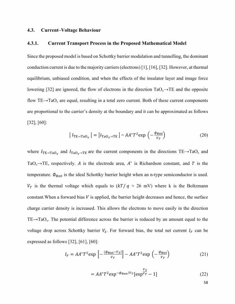
58
4.3. Current–Voltage Behaviour
4.3.1. Current Transport Process in the Proposed Mathematical Model
Since the proposed model is based on Schottky barrier modulation and tunnelling, the dominant
conduction current is due to the majority carriers (electrons) [1], [16], [32]. However, at thermal
equilibrium, unbiased condition, and when the effects of the insulator layer and image force
lowering [32] are ignored, the flow of electrons in the direction TaOx→TE and the opposite
flow TE→TaOx are equal, resulting in a total zero current. Both of these current components
are proportional to the carrier’s density at the boundary and it can be approximated as follows
[32], [60]:
𝐼¥¦→¥§G¨ = 𝐼¥§G¨→¥¦ =𝐴𝐴∗𝑇hexp − «¬w
Oc (20)
where 𝐼¥¦→¥§G¨ and 𝐼¥§G¨→¥¦are the current components in the directions TE→TaOx and
TaOx→TE, respectively. 𝐴 is the electrode area, 𝐴∗ is Richardson constant, and 𝑇 is the
temperature. ∅®¯x is the ideal Schottky barrier height when an n-type semiconductor is used.
𝑉z is the thermal voltage which equals to (𝑘𝑇/𝑞 ≈ 26 mV) where k is the Boltzmann
constant.When a forward bias 𝑉 is applied, the barrier height decreases and hence, the surface
charge carrier density is increased. This allows the electrons to move easily in the direction
TE→TaOx. The potential difference across the barrier is reduced by an amount equal to the
voltage drop across Schottky barrier 𝑉. For forward bias, the total net current 𝐼± can be
expressed as follows [32], [61], [60]:
𝐼± = 𝐴𝐴∗𝑇hexp − («¬w`O²)Oc
− 𝐴𝐴∗𝑇hexp − «¬wOc
(21)
= 𝐴𝐴∗𝑇hexp`«¬w/Oc[exp³²³c − 1] (22)
59
where 𝑉 is given in (13). The first and second terms in (21) are the current components in the
direction TE→TaOx and the opposite direction, respectively. The reverse current can be
obtained using the same expression in (22) but with reversing the polarity of 𝑉 and the
direction of the current [60].
4.3.2. Adding the Effect of the Insulator Layer–TPF
In thin insulators, and under high electric field, the tunnelling process can be the common
carrier conduction mechanism [32], [60]. This is a result of quantum mechanics where the
electron wave function can penetrate through the potential barrier. The insulator between the
metal and semiconductor layers reduces the majority-carriers current and also results in a
higher ideality factor [32] which leads to the deviation from the ideal thermionic emission
mechanism. The proposed mathematical model emphasizes these two deviation effects by
considering the quantum tunnelling in the insulator layer [32], [61], [62]. This tunnelling
mechanism relies on the thickness of the insulator layer as follows.
Very Thin Insulator Layer (<1nm): The carriers do not encounter resistance in the
transporting process and the conduction follows the ideal Schottky contact equation (22).
An Insulator Layer Thickness (>1nm): Tunnelling starts when Ta2O5 thickness is > 1 nm
and the conduction can be assumed to follow the tunnelling process in the MIS system. This
approximation is valid for MISM devices with high electric field and an insulator layer of a
specific thickness only.
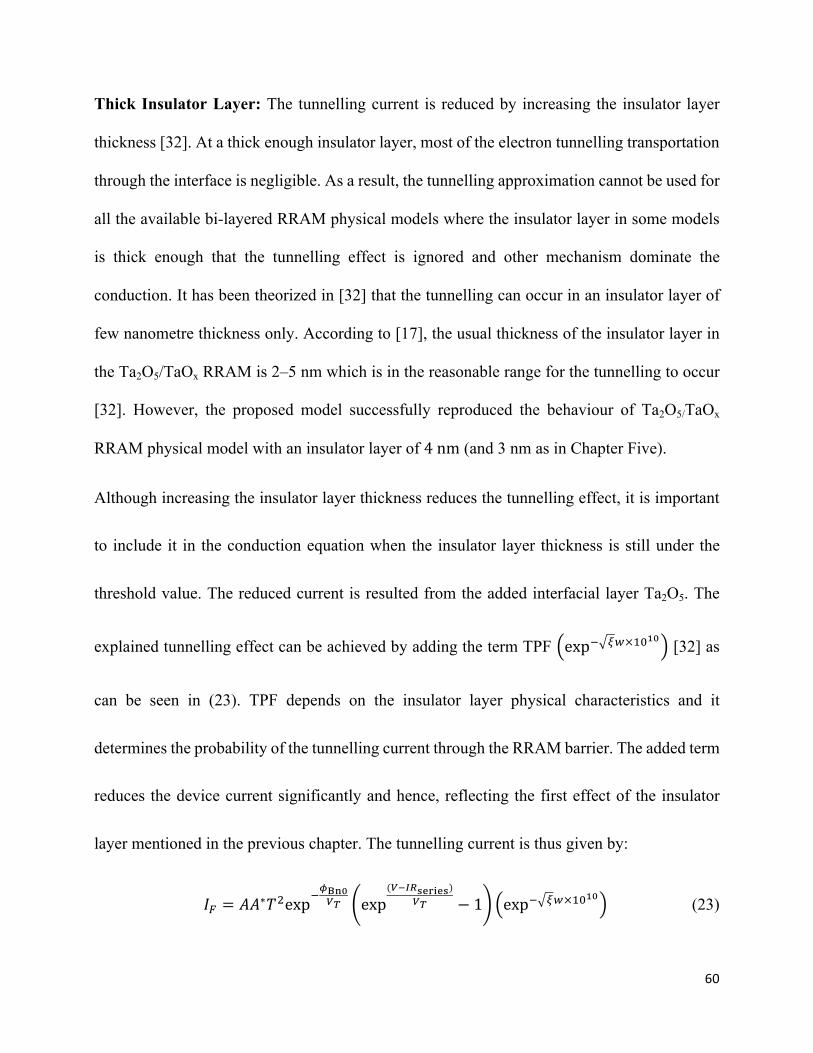
60
Thick Insulator Layer: The tunnelling current is reduced by increasing the insulator layer
thickness [32]. At a thick enough insulator layer, most of the electron tunnelling transportation
through the interface is negligible. As a result, the tunnelling approximation cannot be used for
all the available bi-layered RRAM physical models where the insulator layer in some models
is thick enough that the tunnelling effect is ignored and other mechanism dominate the
conduction. It has been theorized in [32] that the tunnelling can occur in an insulator layer of
few nanometre thickness only. According to [17], the usual thickness of the insulator layer in
the Ta2O5/TaOx RRAM is 2–5 nm which is in the reasonable range for the tunnelling to occur
[32]. However, the proposed model successfully reproduced the behaviour of Ta2O5/TaOx
RRAM physical model with an insulator layer of 4nm (and 3 nm as in Chapter Five).
Although increasing the insulator layer thickness reduces the tunnelling effect, it is important
to include it in the conduction equation when the insulator layer thickness is still under the
threshold value. The reduced current is resulted from the added interfacial layer Ta2O5. The
explained tunnelling effect can be achieved by adding the term TPF exp` µI×gxlw [32] as
can be seen in (23). TPF depends on the insulator layer physical characteristics and it
determines the probability of the tunnelling current through the RRAM barrier. The added term
reduces the device current significantly and hence, reflecting the first effect of the insulator
layer mentioned in the previous chapter. The tunnelling current is thus given by:
𝐼± = 𝐴𝐴∗𝑇hexp`·¬w³c exp
(³k¸¹º»¼¤»º)³c − 1 exp` µI×gxlw (23)
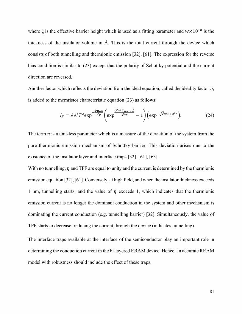
61
where ξ is the effective barrier height which is used as a fitting parameter and 𝑤×10gx is the
thickness of the insulator volume in Å. This is the total current through the device which
consists of both tunnelling and thermionic emission [32], [61]. The expression for the reverse
bias condition is similar to (23) except that the polarity of Schottky potential and the current
direction are reversed.
Another factor which reflects the deviation from the ideal equation, called the ideality factor 𝜂,
is added to the memristor characteristic equation (23) as follows:
𝐼± = 𝐴𝐴∗𝑇hexp`·¬w³c exp
(³k¸¹º»¼¤»º)¾³c − 1 exp` µI×gxlw . (24)
The term 𝜂 is a unit-less parameter which is a measure of the deviation of the system from the
pure thermionic emission mechanism of Schottky barrier. This deviation arises due to the
existence of the insulator layer and interface traps [32], [61], [63].
With no tunnelling, 𝜂 and TPF are equal to unity and the current is determined by the thermionic
emission equation [32], [61]. Conversely, at high field, and when the insulator thickness exceeds
1 nm, tunnelling starts, and the value of 𝜂 exceeds 1, which indicates that the thermionic
emission current is no longer the dominant conduction in the system and other mechanism is
dominating the current conduction (e.g. tunnelling barrier) [32]. Simultaneously, the value of
TPF starts to decrease; reducing the current through the device (indicates tunnelling).
The interface traps available at the interface of the semiconductor play an important role in
determining the conduction current in the bi-layered RRAM device. Hence, an accurate RRAM
model with robustness should include the effect of these traps.
62
4.3.3. The Effect of the Continuous Charging–Discharging of the Interface Traps on the I–V Behaviour
Forming of the Interface Traps: The interface traps in the MIS devices are a property of the
semiconductor layer [62]. However, before going through the modelling of the interface traps
effect in the bi-layered RRAM, it is important to understand how these traps are originally
being formed in the MIS device. The atoms at the surface of the semiconductor layer have
neighbours on one side only and their valence electrons at the vacuum side have no partners
which can be used to form covalent bonds. Instead, these atoms have one unpaired electron
situated in a localized orbital (dangling bond) directed away from the surface [62]. The
interface traps are the electronic states which have been formed by these dangling bonds. The
dangling bonds act as traps and can behave as donors or acceptor by giving up or accepting an
electron, respectively. If the interface traps are occupied up to a certain energy level called the
neutral level (the electrically neutral trapping potential well which can bind only 1 electron or
a hole [61], [64]) and all the states above it are empty, then the semiconductor surface is
electrically neutral. This is considered as a very rare case that seldom occurs in the experimental
results. Thus, usually there are some charges in the interface traps of the RRAM as described
next [62].
The Effect of the Thickness of the Insulator Layer on the Interface Traps Density: As in
the MIS system, for the MISM RRAM studied in this research, the interface traps can be
divided into two groups. The first group can communicate readily with the semiconductor while
the other one communicates with the metal. Hereafter, these groups will be referred to as type
63
1 and 2, respectively. The densities of the groups are function of the insulator layer thickness
(δ). According to this classification, the Ideality factor is given as follows [32], [61]:
𝜂 = 1 + À ÁÂ ÁÃ ÄJlg À ÁÂ JU
(25)
where 𝜀Æ is the dielectric constant of the insulator, 𝜀Ç is the dielectric constant of the bulk layer,
𝑊 is the depletion layer thickness, and 𝐷g and 𝐷h are the interface traps densities of type 1 and
2, respectively. However, the thickness of the insulator layer can alter the interface traps density
and leads to the deviation from the ideal Schottky barrier conduction equation. By knowing
that all the traps are located at the insulator-semiconductor interface, the communication
between 𝐷h and the metal increases for smaller insulator layer while that of 𝐷g increases for
thicker 𝛿. If 𝛿 is thick enough (≥ 3nm), then the value of 𝜂 is largely determined by 𝐷g and
thus, 𝐷h ≈ 0 [32], [61] Equation (25) is reduced to:
𝜂JUx = 1 + 𝛿 𝜀Æ 𝜀Ç 𝑊 + 𝑞𝐷g . (26)
The term 𝛿𝜀Ç 𝑊𝜀Æcan be neglected [61] which would eventually yield a rigorous
interpretation of the interface traps density term 𝜂JUx as follows:
𝜂JUx = 1 + 𝛿 𝜀Æ 𝑞𝐷g . (27)
Since the main contribution to the variation in 𝜂JUx is attributed to the change in 𝐷g, either
(26) or (27) can be used which would eventually lead to the similar approximation. In this case,
𝐷g tends to increase the value of 𝜂JUx [32]. Similarly, if 𝛿 is below 3 nm, most of the interface
traps become in equilibrium with the metal which means that 𝐷g ≈ 0. Equation (25) becomes:
𝜂Jl→x = 1 + À ÁÂ ÁÃ Äg À ÁÂ JU
. (28)
64
In this case, 𝐷h does not have a momentous impact on the value of 𝜂. This can clearly reflect
the fact that when 𝛿 is very small, the value of 𝜂 approaches unity, which represents an ideal
Schottky barrier conduction mechanism. However, since 𝛿 in the proposed RRAM model is
assumed to be 4 nm (the experimental data in [16] is based on 4 nm insulator layer), 𝜂 is
assumed to follow 𝜂JUx.
The Continuous Charging–Discharging of the Interface Traps: The most crucial feature of
the interface traps equation given in (26) is the continuous changing values of 𝐷g and 𝜂JUx
along the RS cycles. When a bias is applied for RS, Fermi level moves continuously up or
down with respect to the interface traps levels where the degree of bending is proportional to
the applied bias [32]. This movement results in a continuous change of the charge of the
interface traps [61] which in turn affects the magnitude of the interface traps density on the
semiconductor, continuously.
During RS, the surface charge carrier density is continuously increased or decreased. However,
since the density of the interface traps 𝐷g increases by increasing the number of mobile charge
carriers moving into the interface [61], [65] which is the case of a forward bias, thereupon, the
values of 𝐷g and hence, 𝜂JUx, continuously increase and decrease as the state is switched to
LRS and HRS, respectively. The values of 𝐷g and 𝜂JUx will reach their maximum value at
LRS (𝑤 = 0) and will start decreasing again toward smaller values once a reverse bias is
applied. These two parameters will reach their minimum values when 𝑤 = 1 at HRS. This
continuous changing mechanism can be modelled as a function of the state variable as follows:
𝜂 = 𝜂JUx,Jl ËÌÍ (1 − IJ) + 𝜂JUx,Jl ÎÌÍ
IJ
(29)
65
where:
𝜂JUx,Jl ËÌÍ = 1 + 𝛿 𝜀Æ 𝑞𝐷g(¡) (30-a)
and
𝜂JUx,Jl ÎÌÍ = 1 + 𝛿 𝜀Æ 𝑞𝐷g (30-b)
where 𝐷g(¡) and 𝐷g() are the interface traps densities at LRS and HRS, respectively.
Nevertheless, there is uncertainty about the value of 𝜀Æ which depends on 𝛿 [61]. Therefore, a
model using the whole equation of𝜂 is difficult to be achieved. The values of 𝜂 at the two
limiting cases of LRS (𝜂¡) and HRS (𝜂) can be estimated by fitting 𝜂 into (24) to get the
best I–V fitting when compared to the measured data in [16] or in other physical model. These
values can then be used in (29) to get the best I–V behaviour for the proposed RRAM when
compared to the experimental results. To get the best fitting results, a fitting parameter m is
added to (29) as follows:
𝜂 = m[ 𝜂¡ (1 −IJ) + 𝜂
IJ] (31)
In this section, it has been shown the impact of the continuous changing of the interface traps
densities located at the semiconductor interface on the bi-layered RRAM current conduction
process during RS cycles. This was achieved by employing the physics of the semiconductor
of the RRAM layers and by relating the thickness of the active oxide layer in the RRAM to the
interface traps densities. The values of the trapped charges are changing as long as the applied
voltage is varying. However, only two discrete values of the interface charges densities and 𝜂
66
do not reflect the actual situation. It is incorrect to assume only two discrete values for these
two parameters at the forward and reverse bias operation.
4.3.4. Adding the Effect of the Image Force Lowering Factor and the Doping Level Variation on Schottky Barrier
The barrier height ∅®¯x is lowered owing to image force lowering [32] and the presence of the
electric field..The image force lowering factor ∆∅ is small compared to the barrier height itself
(𝑞∅®¯x ≈ 0.6𝑒𝑉) and it does not have large impact on the I–V behaviour. The value of ∆∅is
given by [32]:
∆∅ = ÏÐÃÑÒUÁÃÏ
g/Ó (32)
where N is the bulk layer charge density. The value of 𝜑Ç is given by the following equation
[32], [61]:
𝜑Ç = ∅®¯ − ∅Ô ± 𝑉 (33)
where ∅®¯ is the variable Schottky barrier and ∅Ô term has a significantly small value that can
be ignored.
Another factor which influences Schottky barrier in the bi-layered RRAM is the lengths of the
doped and un-doped regions. The resistance of the switching layer decreases/increases by
increasing/decreasing the number of oxygen vacancies in it. As a result, Schottky barrier will
have a variable height and reaches its maximum value at HRS when the number of oxygen
vacancies in the Ta2O5 layer reaches its minimum value. After that, it decreases again during
switching to LRS until it disappears when Ta2O5 layer is fully doped (ohmic contact). Since
67
the doped and un-doped regions of the Ta2O5 layer are corresponding to 𝑤 variation when it is
approaching 0 and 1 respectively, their effect can be modelled as in the following equations:
∅®¯ = ∅®¯xIJ
. (34)
Therefore, Schottky barrier height is reduced by two different factors simultaneously. The main
reduction is determined by the doped and un-doped regions whereby the other factor of image
force lowering involves a significantly smaller effect. These two parameters are combined in
the following equation:
∅ = ∅®¯ − ∆∅. (35)
∅ = ∅®¯xIJ
- ÏÐÃÑÒUÁÃÏ
g/Ó. (36)
In (33), since ∅Ôis significantly smaller than the other two parameters in the equation [7], it
can be ignored. In addition to that, (33) was stated in [32] and [60] to represent the potential
barrier for an MIS system in which Schottky barrier height depends on the applied voltage.
However, in the proposed model, since Schottky barrier value is changing according to the
doped and un-doped regions which in turn depends on the voltage, then the effect of the applied
voltage is already being incorporated and can be ignored in (33). Thus:
𝜑Ç ≈ ∅®¯. (37)
After introducing Schottky barrier lowering effects and the ideality factor into (24), the
Ta2O5/TaOx RRAM I–V equation becomes:
𝐼 = 𝐴𝐴∗𝑇hexp`(Ôl,U∅Ö)/Oc exp(³k¸¹º»¼¤»º)
¾³c − 1 exp` µI×gxlw . (38)
68
Equation (38) represent the electronic current not the ionic current (which only has a very
specific transient current during the switching event). However, for the simplification of the
model, we assumed that 𝑇0 is the device temperature when it is not in the switching stage (at
LRS or HRS) and hence, 𝑇0 is used in (38). 𝑛1 and 𝑛2 are fitting parameters that determine the
influence of ∅𝑏 on 𝐼.
4.4. Temperature Modelling
During RS process, the formation and rupture of the CF are sensitive to the temperature. Thus,
the temperature effect is important during the RS behaviour and should be considered in the
CF growth rate equation. The temperature in the simulation is the local temperature around the
doped region which can be raised during the RS due to Joule heating effect [66]. This enhances
the ions migration process and thus, it should be used in the growth rate equation. For the
simplification of the model and since the current work focuses on other physics aspects, the
approximate value of the temperature used in this model is based on the simple analysis in [58]
and [66]. A complete electro-thermal analysis has already presented in the literature and can
be used in the future work. The doped region temperature is given by [66]:
𝑇 = 𝑇x + 𝐼h ∙ 𝑅 ∙ 𝑅×Ø (39)
where 𝑇x is the ambient temperature, 𝑅×Ø is the effective thermal resistance, 𝑅 is the doped
region electrical resistance, and I is the current through that region.
69
4.5. Bi-Layered RRAM Device Simulation and Results Discussion
The RRAM equations provided in sections 4.2–4.4 have been evaluated by simulation using
MATLAB. The full MATLAB code is provided in Appendix A. The device coefficients used
during the simulation includes the following:𝑅GH = 1.7kΩ,𝑅X = 12kΩ, 𝑅GKK = 40kΩs,
𝐷 = 4nm, 𝐴 = 9×10`Ýcmh, 𝐴∗ = 120×10ÓA ∙ m`h ∙ K`h, ∅®¯x = 0.6eV, 𝑐 = 1×
10gáHz, 𝑈 = 1eV, 𝑥g = 175, 𝑥h = 0.4, 𝑇x = 300K, and 𝑎 = 1nm [67] which can be used as
fitting parameter to account for the un-doped region growth velocity. The initial conditions
presumed that the RRAM state is at LRS with an initial resistance 𝑅 = 𝑅GH + 𝑅X and
𝑤 = 0nm. The proposed model is correlated against several published characteristics of the
Pt/Ta2O5/TaOx/Pt RRAM and a number of different insights and matched features emerged.
4.5.1. Relationship and the Agreement with the LRS/HRS Switching Behaviour
4.5.1.1. Non-Linear Ionic Drift Mechanism
Figure 4.2 shows the measured data for the fabricated Pt/Ta2O5/TaOx/Pt [16] compared with
the simulated semi-log scale plot of the I–V characteristic of the BRS mathematical proposed
model for both SET and RESET processes. It can be seen that the device is switching to LRS
and HRS periodically by a 100 Hz sine wave, SET voltage of -2 V and 3 V RESET voltages
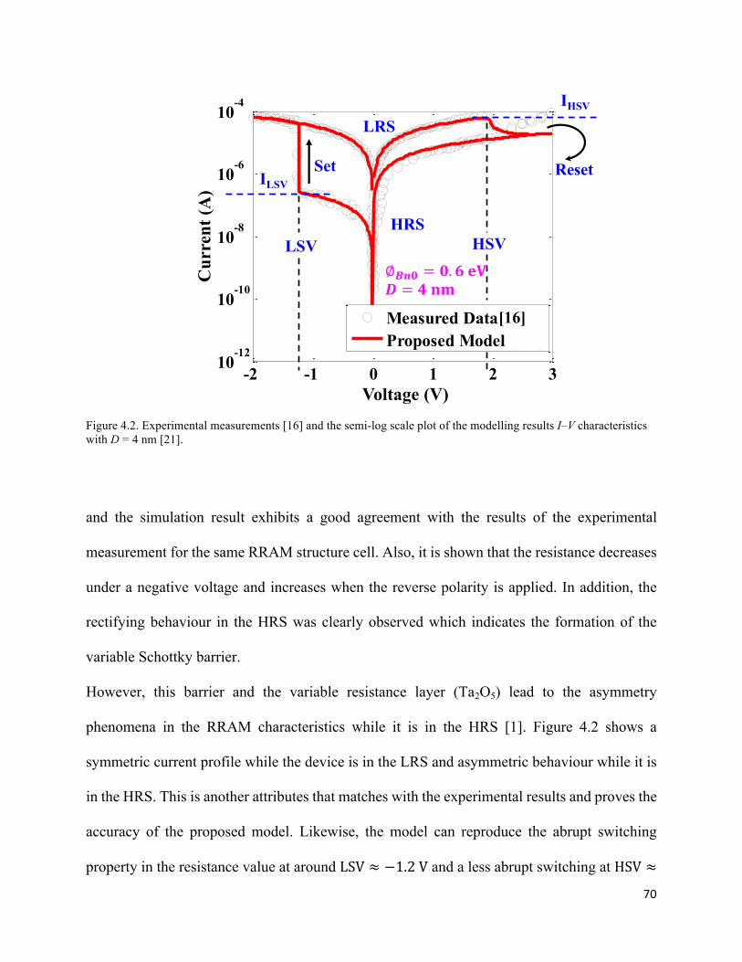
70
Figure 4.2. Experimental measurements [16] and the semi-log scale plot of the modelling results I–V characteristics with D = 4 nm [21].
and the simulation result exhibits a good agreement with the results of the experimental
measurement for the same RRAM structure cell. Also, it is shown that the resistance decreases
under a negative voltage and increases when the reverse polarity is applied. In addition, the
rectifying behaviour in the HRS was clearly observed which indicates the formation of the
variable Schottky barrier.
However, this barrier and the variable resistance layer (Ta2O5) lead to the asymmetry
phenomena in the RRAM characteristics while it is in the HRS [1]. Figure 4.2 shows a
symmetric current profile while the device is in the LRS and asymmetric behaviour while it is
in the HRS. This is another attributes that matches with the experimental results and proves the
accuracy of the proposed model. Likewise, the model can reproduce the abrupt switching
property in the resistance value at around LSV ≈ −1.2V and a less abrupt switching at HSV ≈
-2 -1 0 1 2 310
-12
10-10
10-8
10-6
10-4
Measured DataProposed Model [ ]
Voltage (V)
HSVLSV
Set Reset
LRS
HRSC
urre
nt (A
)
∅𝑩𝒏𝟎 = 𝟎. 𝟔𝐞𝐕𝑫 = 𝟒𝐧𝐦
IHSV
ILSV
[16]
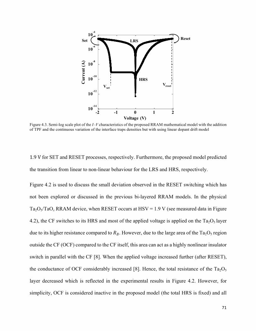
71
Figure 4.3. Semi-log scale plot of the I–V characteristics of the proposed RRAM mathematical model with the addition of TPF and the continuous variation of the interface traps densities but with using linear dopant drift model
1.9V for SET and RESET processes, respectively. Furthermore, the proposed model predicted
the transition from linear to non-linear behaviour for the LRS and HRS, respectively.
Figure 4.2 is used to discuss the small deviation observed in the RESET switching which has
not been explored or discussed in the previous bi-layered RRAM models. In the physical
Ta2O5/TaOx RRAM device, when RESET occurs at HSV = 1.9 V (see measured data in Figure
4.2), the CF switches to its HRS and most of the applied voltage is applied on the Ta2O5 layer
due to its higher resistance compared to 𝑅𝐵. However, due to the large area of the Ta2O5 region
outside the CF (OCF) compared to the CF itself, this area can act as a highly nonlinear insulator
switch in parallel with the CF [8]. When the applied voltage increased further (after RESET),
the conductance of OCF considerably increased [8]. Hence, the total resistance of the Ta2O5
layer decreased which is reflected in the experimental results in Figure 4.2. However, for
simplicity, OCF is considered inactive in the proposed model (the total HRS is fixed) and all
0 0.02 0.04 0.060
0.2
0.4
0.6
0.8
1
Time (sec)
W(t)
/D
W/D
0 0.02 0.04 0.06-2
-1.5
-1
-0.5
0
0.5
1
1.5
2V-t curve
T[Sec]
V[Vo
lts]
0 0.02 0.04 0.06-4
-3
-2
-1
0
1
2
3
4x 10⁻⁵ I-t curve
T[Sec]
I[Am
ps]
-2 -1 0 1 2-4
-2
0
2
4x 10⁻⁵
Voltage (V)
Cur
rent
(A)
-2 -1 0 1 210
-14
10-12
10-10
10-8
10-6
10-4
Voltage (V)
Cur
rent
(A)
0 0.02 0.04 0.060
20
40
60
80
100Eta-Time curve
[Sec]
Eta
0 0.02 0.04 0.06-1
-0.5
0
0.5
1
1.5
2x 10⁹ V./Itun-t curve
T[Sec]
V./It
un[O
hm]
-2 -1 0 1 2-0.1
0
0.1
0.2
0.3
0.4
0.5
0.6V-PhiB
V[Volts]
Phi B[e
V]
VresetVset
Set ResetLRS
HRS
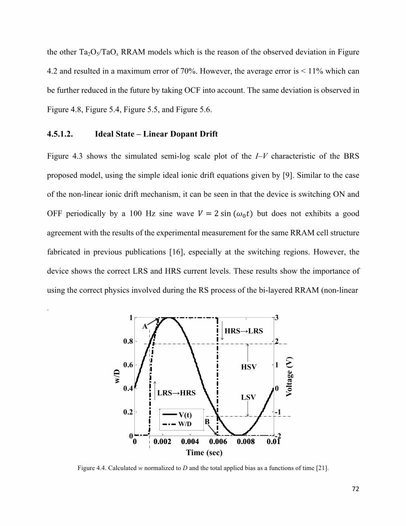
72
the other Ta2O5/TaOx RRAM models which is the reason of the observed deviation in Figure
4.2 and resulted in a maximum error of 70%. However, the average error is < 11% which can
be further reduced in the future by taking OCF into account. The same deviation is observed in
Figure 4.8, Figure 5.4, Figure 5.5, and Figure 5.6.
4.5.1.2. Ideal State – Linear Dopant Drift Figure 4.3 shows the simulated semi-log scale plot of the I–V characteristic of the BRS
proposed model, using the simple ideal ionic drift equations given by [9]. Similar to the case
of the non-linear ionic drift mechanism, it can be seen in that the device is switching ON and
OFF periodically by a 100 Hz sine wave 𝑉 = 2sin(𝜔x𝑡) but does not exhibits a good
agreement with the results of the experimental measurement for the same RRAM cell structure
fabricated in previous publications [16], especially at the switching regions. However, the
device shows the correct LRS and HRS current levels. These results show the importance of
using the correct physics involved during the RS process of the bi-layered RRAM (non-linear
.
Figure 4.4. Calculated w normalized to D and the total applied bias as a functions of time [21].
0 0.002 0.004 0.006 0.008 0.010
0.2
0.4
0.6
0.8
1
W(t)
/D
0 0.002 0.004 0.006 0.008 0.01-2
-1
0
1
2
3
Vol
tage
(V)
V(t)W(t)/D
HSV
LSV
WR
CF/
D
W/D
HRS→LRS
LRS→HRS
B
A
Time (sec)
w/D
Volta
ge (V
)
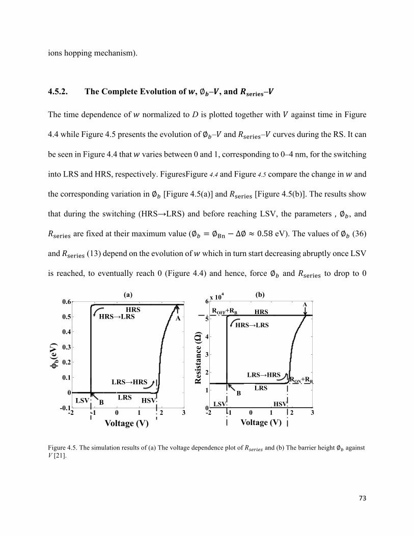
73
ions hopping mechanism).
4.5.2. The Complete Evolution of 𝒘, ∅𝒃–𝑽, and 𝑹𝐬𝐞𝐫𝐢𝐞𝐬–𝑽
The time dependence of 𝑤 normalized to D is plotted together with 𝑉 against time in Figure
4.4 while Figure 4.5 presents the evolution of ∅–𝑉 and 𝑅–𝑉 curves during the RS. It can
be seen in Figure 4.4 that 𝑤 varies between 0 and 1, corresponding to 0–4 nm, for the switching
into LRS and HRS, respectively. FiguresFigure 4.4 and Figure 4.5 compare the change in 𝑤 and
the corresponding variation in ∅ [Figure 4.5(a)] and 𝑅 [Figure 4.5(b)]. The results show
that during the switching (HRS→LRS) and before reaching LSV, the parameters , ∅, and
𝑅 are fixed at their maximum value (∅ = ∅®¯ − ∆∅ ≈ 0.58 eV). The values of ∅ (36)
and 𝑅 (13) depend on the evolution of 𝑤 which in turn start decreasing abruptly once LSV
is reached, to eventually reach 0 (Figure 4.4) and hence, force ∅ and 𝑅 to drop to 0
Figure 4.5. The simulation results of (a) The voltage dependence plot of 𝑅ÇïïÇ and (b) The barrier height ∅ against V [21].
-2 -1 0 1 2 30
1
2
3
4
5
6 x 10⁴
Voltage (V)
Res
ista
nce(W)
HRS
LRS
ROFF+RB
RON+RB
HSVLSV
A
B
HRS→LRS
LRS→HRS
Res
ista
nce
(Ω)
Voltage (V)-2 -1 0 1 2 3
-0.1
0
0.1
0.2
0.3
0.4
0.5
0.6
Voltage (V)
b (e
V)
f
HRS
LRS HSVLSV
A
B
HRS→LRS
LRS→HRS
Voltage (V)
ϕ b(e
V)
(a) (b)
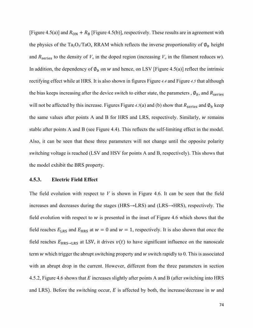
74
[Figure 4.5(a)] and 𝑅GH + 𝑅® [Figure 4.5(b)], respectively. These results are in agreement with
the physics of the Ta2O5/TaOx RRAM which reflects the inverse proportionality of ∅ height
and 𝑅 to the density of Vo in the doped region (increasing Vo in the filament reduces 𝑤).
In addition, the dependency of ∅ on 𝑤 and hence, on LSV [Figure 4.5(a)] reflect the intrinsic
rectifying effect while at HRS. It is also shown in figures Figure 4.4 and Figure 4.5 that although
the bias keeps increasing after the device switch to either state, the parameters , ∅, and 𝑅
will not be affected by this increase. Figures Figure 4.5(a) and (b) show that 𝑅 and ∅ keep
the same values after points A and B for HRS and LRS, respectively. Similarly, 𝑤 remains
stable after points A and B (see Figure 4.4). This reflects the self-limiting effect in the model.
Also, it can be seen that these three parameters will not change until the opposite polarity
switching voltage is reached (LSV and HSV for points A and B, respectively). This shows that
the model exhibit the BRS property.
4.5.3. Electric Field Effect
The field evolution with respect to V is shown in Figure 4.6. It can be seen that the field
increases and decreases during the stages (HRS→LRS) and (LRS→HRS), respectively. The
field evolution with respect to 𝑤 is presented in the inset of Figure 4.6 which shows that the
field reaches 𝐸¡ and 𝐸 at 𝑤 = 0 and 𝑤 = 1, respectively. It is also shown that once the
field reaches 𝐸→¡ at LSV, it drives 𝑣(𝑡) to have significant influence on the nanoscale
term 𝑤 which trigger the abrupt switching property and 𝑤 switch rapidly to 0. This is associated
with an abrupt drop in the current. However, different from the three parameters in section
4.5.2, Figure 4.6 shows that 𝐸 increases slightly after points A and B (after switching into HRS
and LRS). Before the switching occur, 𝐸 is affected by both, the increase/decrease in 𝑤 and
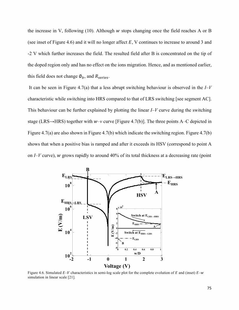
75
the increase in V, following (10). Although 𝑤 stops changing once the field reaches A or B
(see inset of Figure 4.6) and it will no longer affect 𝐸, V continues to increase to around 3 and
-2 V which further increases the field. The resulted field after B is concentrated on the tip of
the doped region only and has no effect on the ions migration. Hence, and as mentioned earlier,
this field does not change ∅, and 𝑅.
It can be seen in Figure 4.7(a) that a less abrupt switching behaviour is observed in the I–V
characteristic while switching into HRS compared to that of LRS switching [see segment AC].
This behaviour can be further explained by plotting the linear I–V curve during the switching
stage (LRS→HRS) together with 𝑤–v curve [Figure 4.7(b)]. The three points A–C depicted in
Figure 4.7(a) are also shown in Figure 4.7(b) which indicate the switching region. Figure 4.7(b)
shows that when a positive bias is ramped and after it exceeds its HSV (correspond to point A
on I–V curve), 𝑤 grows rapidly to around 40% of its total thickness at a decreasing rate (point
Figure 4.6. Simulated 𝐸–𝑉 characteristics in semi-log scale plot for the complete evolution of 𝐸 and (inset) 𝐸–𝑤 simulation in linear scale [21].
-2 -1 0 1 2 3102
104
106
108
Voltage (V)
E (V
/m)
HSV
LSV
EHRS
ELRS
B
EHRS→LRS
ELRS→HRS
A
E(V
/m)
Voltage (V)
0 0.2 0.4 0.6 0.8 1-8
-6
-4
-2
0
2
4
6
8 x 10⁸
W/D
E (V
/m)
w/D
ELRS
Switch at ELRS→HRS
B
EHRSA
E(V
/m)
Switch at EHRS→LRS
76
B on I–V curve) before its growth rate continues dropping further at a higher rate for the
remaining length (correspond to segment BC in I–V curve). This mechanism is reflected in the
proposed model in the sinh dependency of 𝑣(𝑡) on the evolution of 𝐸. As the doped region
length decreases due to oxygen ions migration into Ta2O5 layer, 𝐸 on the increasing length of
𝑤 keeps dropping, following (10), and strongly slowing down 𝑣(𝑡). This behaviour explains
the corresponding drop in the current during this switching stage. It also can explain the reason
of using a higher RESET voltage compared to the SET process to avoid self-limiting effect due
to the small remaining 𝐸 and to rupture the whole CF during the required time.
The observed small deviation during the switching stage LRS→HRS (see Figure 4.2) can be
attributed to different possible factors. Some oxygen ions might come from the sides of the
Figure 4.7. (a) Simulation results of I–V curve in semi-log scale plot and (b) Simulated linear I–V and 𝑤–𝑉 curves for the LRS→HRS switching stage [21].
doped region [18] during the RS. Besides that, the ionic drift in the oxides may include a
complex interplay of drift, diffusion, and thermophoresis [7].
w/D
0 1 2 30
0.5
1x 10⁻⁴
0 1 2 30
0.5
1Current
Cur
rent
(A)
Voltage (V)
w/D
B
HSV
C
A
0 1 2 310-9
10-8
10-7
10-6
10-5
10-4
HSV
LRS→HRS
BA
C
Cur
rent
(A)
Voltage (V)
(a) (b)
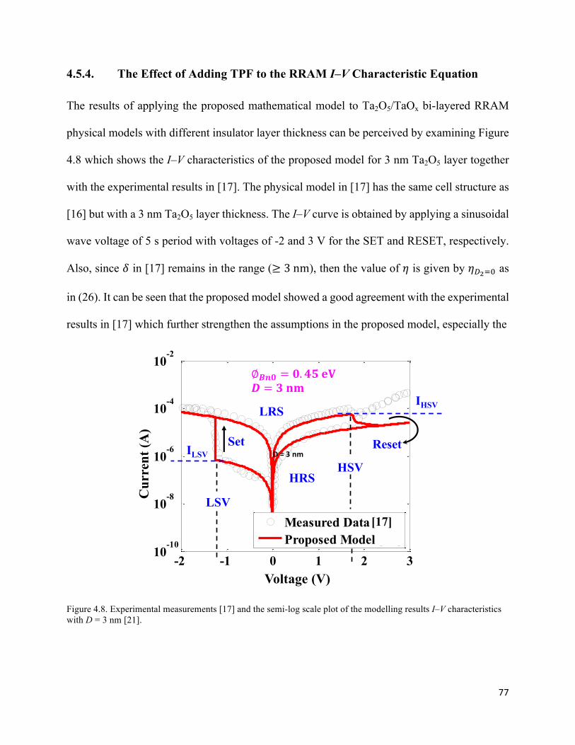
77
4.5.4. The Effect of Adding TPF to the RRAM I–V Characteristic Equation
The results of applying the proposed mathematical model to Ta2O5/TaOx bi-layered RRAM
physical models with different insulator layer thickness can be perceived by examining Figure
4.8 which shows the I–V characteristics of the proposed model for 3 nm Ta2O5 layer together
with the experimental results in [17]. The physical model in [17] has the same cell structure as
[16] but with a 3 nm Ta2O5 layer thickness. The I–V curve is obtained by applying a sinusoidal
wave voltage of 5 s period with voltages of -2 and 3 V for the SET and RESET, respectively.
Also, since 𝛿 in [17] remains in the range (≥ 3nm), then the value of 𝜂 is given by 𝜂JUx as
in (26). It can be seen that the proposed model showed a good agreement with the experimental
results in [17] which further strengthen the assumptions in the proposed model, especially the
Figure 4.8. Experimental measurements [17] and the semi-log scale plot of the modelling results I–V characteristics with D = 3 nm [21].
-2 -1 0 1 2 310
-10
10-8
10-6
10-4
10-2
Measured DataProposed Model [ ]
Voltage (V)
HSV
LSV
Reset
LRS
HRS
Cur
rent
(A)
∅𝑩𝒏𝟎 = 𝟎. 𝟒𝟓𝐞𝐕𝑫 = 𝟑𝐧𝐦
IHSV
ILSVSet
[17]
D=3nm
78
TPF approximation. Thus, significant improvement to the proposed model is achieved by
adding TPF term. When the RRAM model is developed by taking into account the insulator
layer thickness and tunnelling current, TPF emphasizes the dependency of the RRAM current
values on the physical characteristics of the insulator layer. Without adding TPF, the current
equation follows the standard Schottky barrier conduction equation for metal-semiconductor
system, which leads to considerably larger values than the corresponding experimental results.
4.5.5. The Agreement of the Proposed Model to the Attributes of the Zero-Crossing Behaviour for the Memristive System
The proposed RRAM model elucidated another important property of the memristive devices
identified in [9] and [16] which is the zero-crossing behaviour. This means that, regardless of
the RRAM resistance, the frequency of the applied input signal, or the state variable values 𝑤,
the RRAM output current is always zero when the input voltage reaches zero. As it can be
clearly seen in figures Figure 4.2 and Figure 4.8 for the applied periodical input voltages, the
attained property is satisfied in the I–V characteristics of the proposed RRAM model, regardless
of the values of the three parameters mentioned above.
79
5. Chapter Five: SPICE Modelling of Ta2O5/TaOx Bi-Layered RRAM
SPICE MODELLING OF Ta2O5/TaOx Bi-Layered
RRAM
Related Publications: F. O. Hatem, T. N. Kumar, and H. A. F. Almurib, “A SPICE Model of the Ta2O5/TaOx Bi-Layered RRAM,” IEEE Transactions on Circuits and Systems I: Regular Papers, vol. 63, no. 9, pp. 1487-1498. 2016.
80
Summary
Designing a SPICE model is a critical step toward understanding the behaviour of the RRAM
devices when integrated in memory design for the future generation storage devices. In this
chapter, a SPICE model is developed for the Ta2O5/TaOx bi-layered RRAM. The proposed
model emphasizes the impact of the change in the switching layer thickness on the device
behaviour at LRS, HRS, and the transitional period. The validity of the proposed model is
verified through using three different sets of experimental data from Pt/Ta2O5/TaOx/Pt RRAM
with switching layer thickness smaller than 5 nm. The SPICE model reproduced all the major
features from the experimental results for the SET and RESET processes and also the
asymmetric and the symmetric characteristics in HRS and LRS, respectively. The proposed
SPICE model matches the measured experimental results with an average error of < 11% and
a maximum error of < 70%. It also showed stable behaviour for its HRS and LRS regions under
different types of input signals. The model is parameterized in order to fit into Ta2O5/TaOx
RRAM devices with switching layer thickness smaller than 5 nm, thus, facilitating the model
usage. The model can be included in the SPICE-compatible circuit simulation and is suitable
for the exploration of the Ta2O5/TaOx bi-layered RRAM device performance at circuit level.
The obtained simulation results show that the proposed SPICE model can successfully
demonstrate four intrinsic features extracted from the experimental observations of the
Ta2O5/TaOx RRAM in which the first three features are related directly to the change in D. 1)
The model is first verified that it can produce the correct I–V behaviour when D is changed
from 4 to 3 nm. 2) The model is then proved that it can demonstrate the dependency of the
HSV on D where HSV is the required voltage for the device to switch into HRS. 3) The ability
of the SPICE model to demonstrate the effect of changing D on its LRS and HRS is also
81
explored. 4) The model is examined and verified that it can successfully capture the temporal
increase in the HRS during SET switching; an important intrinsic feature of the P/Ta2O5
interface which has been reported in [1]. To further verify the validity of the proposed SPICE
model, pulse switching simulation with different RESET pulse amplitudes is conducted. The
simulation results match with the measured data and show that the model can successfully
demonstrate the change in the current with regards to RESET pulse amplitude. Also, the SPICE
model is tested for predicting the correct RS behaviour for different types of the conventional
voltage signals. The proposed model provided full RS switching with the same LRS and HRS
value despite the type of the stimulus signal. As a final verification step, the integration
capability of the proposed SPICE model with the CMOS technology is tested by simulating a
non-volatile D-Latch circuit.
To the best of the researcher’s knowledge, this is the first Ta2O5/TaOx bi-layered RRAM
physics-based model that has been implemented as SPICE subcircuit, correlated to more than
one thickness, successfully verified using the above intrinsic features, and proved to show a
stable behaviour for sinusoidal, rectangular, and triangular inputs. This SPICE model can be
used for the bi-layered RRAM-based circuit applications, providing more flexibility in the used
device thickness and the bias signal. The proposed model can be considered as a first step
approach into finding a more universal SPICE model that can predict the behaviour of the bi-
layered RRAM devices with different oxide materials and thicker switching layers (thicker
than 4 nm).
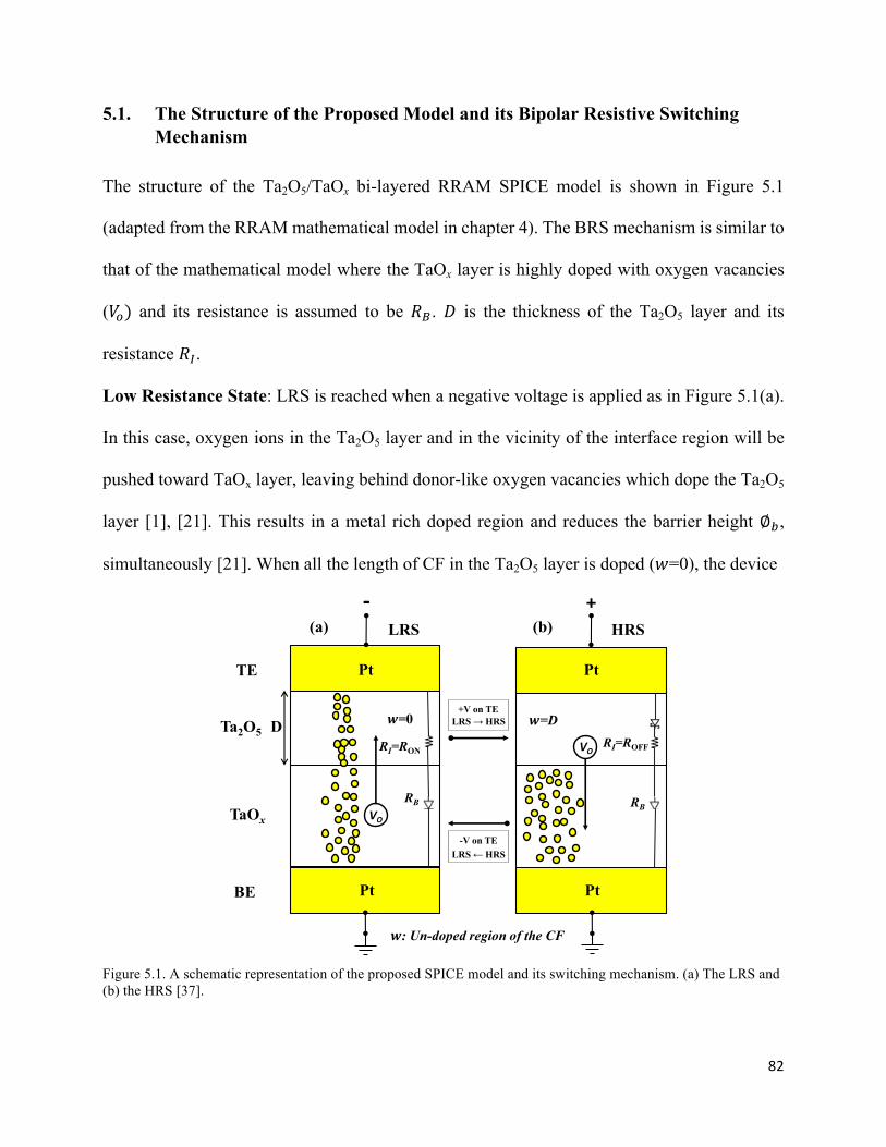
82
5.1. The Structure of the Proposed Model and its Bipolar Resistive Switching Mechanism
The structure of the Ta2O5/TaOx bi-layered RRAM SPICE model is shown in Figure 5.1
(adapted from the RRAM mathematical model in chapter 4). The BRS mechanism is similar to
that of the mathematical model where the TaOx layer is highly doped with oxygen vacancies
(𝑉Æ) and its resistance is assumed to be 𝑅X. 𝐷 is the thickness of the Ta2O5 layer and its
resistance 𝑅Y.
Low Resistance State: LRS is reached when a negative voltage is applied as in Figure 5.1(a).
In this case, oxygen ions in the Ta2O5 layer and in the vicinity of the interface region will be
pushed toward TaOx layer, leaving behind donor-like oxygen vacancies which dope the Ta2O5
layer [1], [21]. This results in a metal rich doped region and reduces the barrier height ∅,
simultaneously [21]. When all the length of CF in the Ta2O5 layer is doped (𝑤=0), the device
Figure 5.1. A schematic representation of the proposed SPICE model and its switching mechanism. (a) The LRS and (b) the HRS [37].
TE
BE
Ta2O5
TaOx
Pt
Pt
+
D 𝒘=0
HRS LRS
VO
-
RB
RI=RON
Pt
Pt
VO
RB
RI=ROFF
(b)(a)
-V on TELRS ← HRS
+V on TELRS → HRS 𝒘=D
𝒘: Un-doped region of the CF
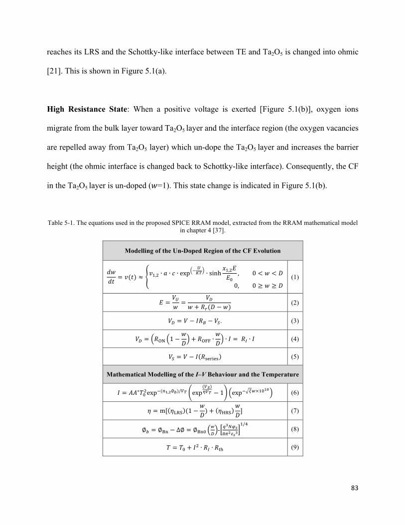
83
reaches its LRS and the Schottky-like interface between TE and Ta2O5 is changed into ohmic
[21]. This is shown in Figure 5.1(a).
High Resistance State: When a positive voltage is exerted [Figure 5.1(b)], oxygen ions
migrate from the bulk layer toward Ta2O5 layer and the interface region (the oxygen vacancies
are repelled away from Ta2O5 layer) which un-dope the Ta2O5 layer and increases the barrier
height (the ohmic interface is changed back to Schottky-like interface). Consequently, the CF
in the Ta2O5 layer is un-doped (𝑤=1). This state change is indicated in Figure 5.1(b).
Table 5-1. The equations used in the proposed SPICE RRAM model, extracted from the RRAM mathematical model in chapter 4 [37].
Modelling of the Un-Doped Region of the CF Evolution
𝑑𝑤𝑑𝑡
= 𝑣(𝑡) ≈ 𝑣g,h ∙ 𝑎 ∙ 𝑐 ∙ exp` yz ∙ sinh
𝑥g,h𝐸𝐸x
, 0 < 𝑤 < 𝐷
0, 0 ≥ 𝑤 ≥ 𝐷 (1)
𝐸 =𝑉𝑤=
𝑉J𝑤 + 𝑅(𝐷 − 𝑤)
(2)
𝑉J = 𝑉 − 𝐼𝑅X − 𝑉. (3)
𝑉J = 𝑅GH 1 −𝑤𝐷
+ 𝑅GKK ∙𝑤𝐷
∙ 𝐼 = 𝑅Y ∙ 𝐼 (4)
𝑉 = 𝑉 − 𝐼 𝑅 (5)
Mathematical Modelling of the I–V Behaviour and the Temperature
𝐼 = 𝐴𝐴∗𝑇xhexp`(Ôl,U∅Ö)/Oc exp(O²)ðOc − 1 exp` µI×gxlw (6)
𝜂 = m[ 𝜂¡ (1 −𝑤𝐷) + 𝜂
𝑤𝐷] (7)
∅ = ∅®¯ − ∆∅ = ∅®¯xIJ
- ÏÐÃÑÒUÁÃÏ
g/Ó (8)
𝑇 = 𝑇x + 𝐼h ∙ 𝑅Y ∙ 𝑅×Ø (9)
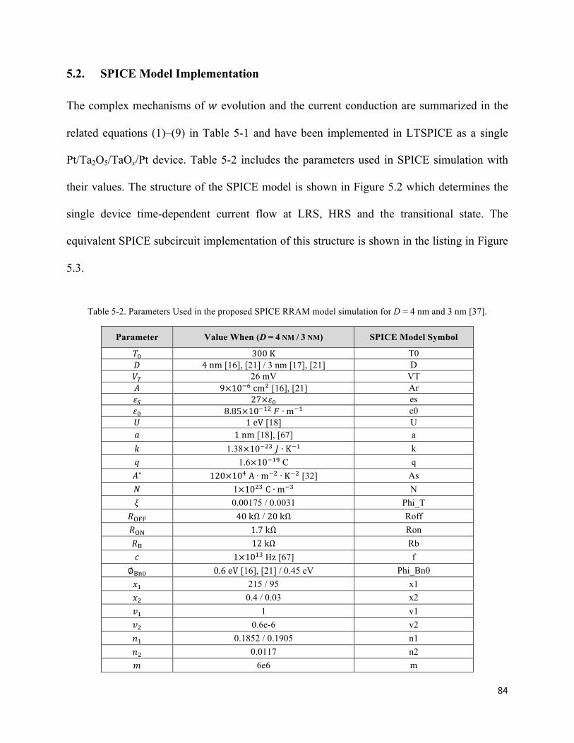
84
5.2. SPICE Model Implementation
The complex mechanisms of 𝑤 evolution and the current conduction are summarized in the
related equations (1)–(9) in Table 5-1 and have been implemented in LTSPICE as a single
Pt/Ta2O5/TaOx/Pt device. Table 5-2 includes the parameters used in SPICE simulation with
their values. The structure of the SPICE model is shown in Figure 5.2 which determines the
single device time-dependent current flow at LRS, HRS and the transitional state. The
equivalent SPICE subcircuit implementation of this structure is shown in the listing in Figure
5.3.
Table 5-2. Parameters Used in the proposed SPICE RRAM model simulation for D = 4 nm and 3 nm [37].
Parameter Value When (D = 4 NM / 3 NM) SPICE Model Symbol
𝑇x 300K T0 𝐷 4nm [16], [21] / 3 nm [17], [21] D 𝑉z 26 mV VT 𝐴 9×10`Ýcmh [16], [21] Ar 𝜀 27×𝜀x es 𝜀x 8.85×10`gh𝐹 ∙ m`g e0 𝑈 1eV [18] U 𝑎 1nm [18], [67] a 𝑘 1.38×10`há 𝐽 ∙ K`g k 𝑞 1.6×10`gó C q 𝐴∗ 120×10ÓA ∙ m`h ∙ K`h [32] As 𝑁 1×10há C ∙ m`á N 𝜉 0.00175 / 0.0031 Phi_T
𝑅GKK 40kΩ / 20kΩ Roff 𝑅GH 1.7kΩ Ron 𝑅® 12kΩ Rb 𝑐 1×10gáHz [67] f
∅®¯x 0.6eV [16], [21] / 0.45 eV Phi_Bn0 𝑥g 215 / 95 x1 𝑥h 0.4 / 0.03 x2 𝑣g 1 v1 𝑣h 0.6e-6 v2 𝑛g 0.1852 / 0.1905 n1 𝑛h 0.0117 n2 𝑚 6e6 m
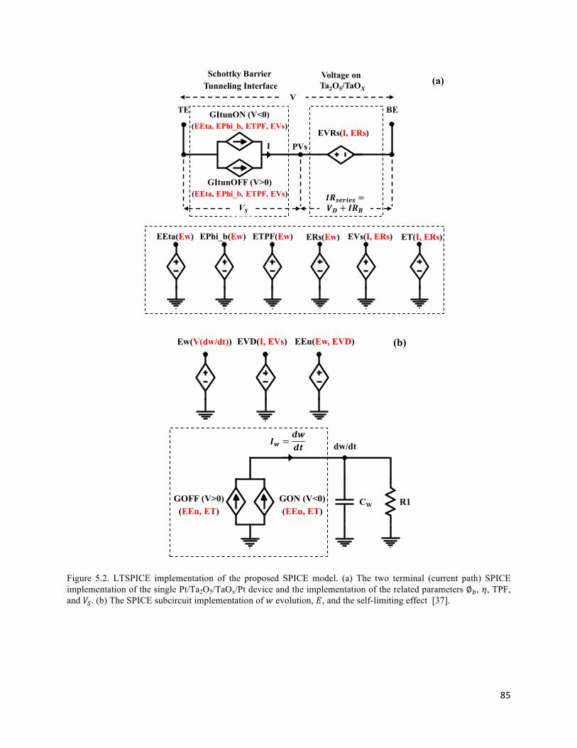
85
Figure 5.2. LTSPICE implementation of the proposed SPICE model. (a) The two terminal (current path) SPICE implementation of the single Pt/Ta2O5/TaOx/Pt device and the implementation of the related parameters ∅, 𝜂, TPF, and 𝑉. (b) The SPICE subcircuit implementation of 𝑤 evolution, 𝐸, and the self-limiting effect [37].
GItunON (V<0)(EEta, EPhi_b, ETPF, EVs)
GItunOFF (V>0)(EEta, EPhi_b, ETPF, EVs)
TE BE
EVRs(I, ERs)PVs
Schottky BarrierTunneling Interface
VS
V
𝑰𝑹𝒔𝒆𝒓𝒊𝒆𝒔 =𝑽𝑫 + 𝑰𝑹𝑩
Voltage on Ta2O5/TaOX
I
EVs(I, ERs)ETPF(Ew)EPhi_b(Ew)EEta(Ew) ERs(Ew) ET(I, ERs)
(a)
GON (V<0)(EEu, ET)
EEu(Ew, EVD)
dw/dt
CW R1GOFF (V>0)(EEu, ET)
𝑰𝒘 =𝒅𝒘𝒅𝒕
EVD(I, EVs) (b)Ew(V(dw/dt))
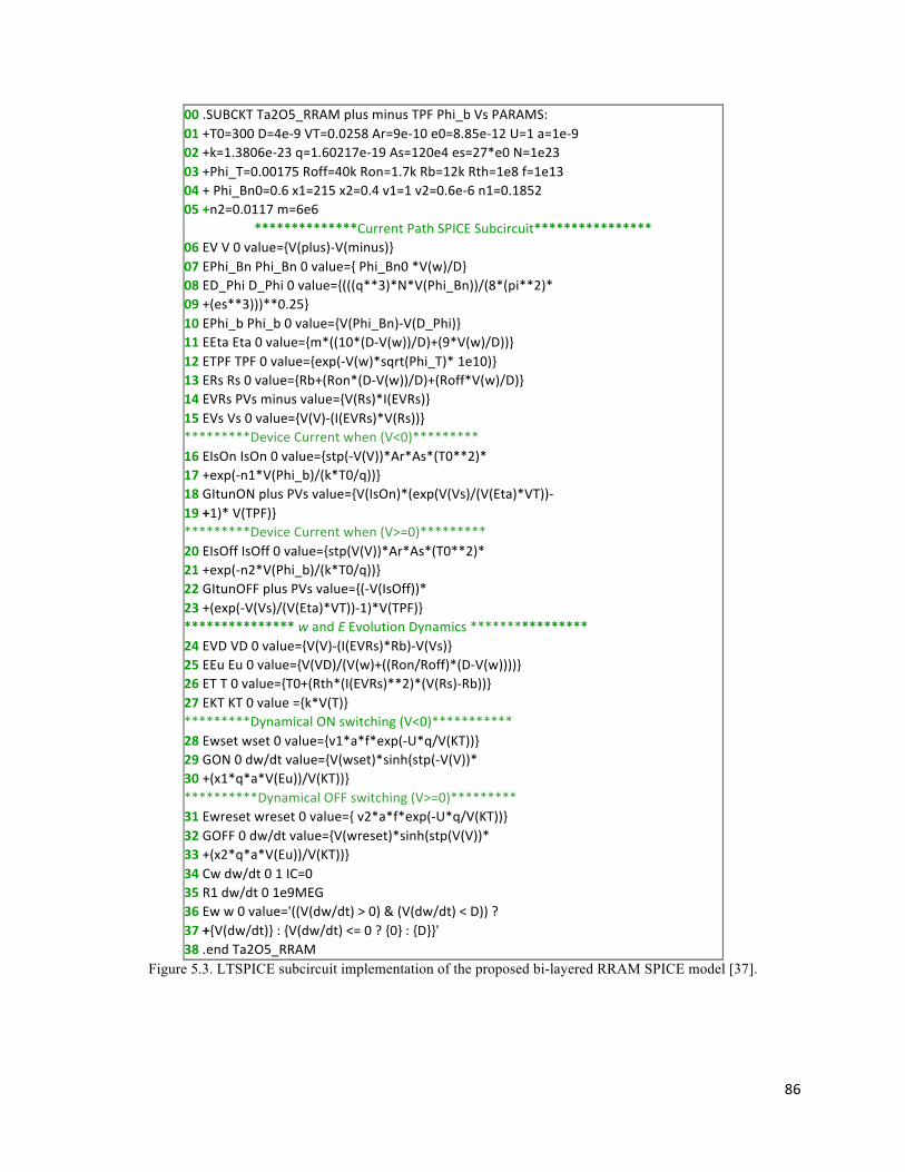
86
00.SUBCKTTa2O5_RRAMplusminusTPFPhi_bVsPARAMS:01+T0=300D=4e-9VT=0.0258Ar=9e-10e0=8.85e-12U=1a=1e-902+k=1.3806e-23q=1.60217e-19As=120e4es=27*e0N=1e2303+Phi_T=0.00175Roff=40kRon=1.7kRb=12kRth=1e8f=1e1304+Phi_Bn0=0.6x1=215x2=0.4v1=1v2=0.6e-6n1=0.185205+n2=0.0117m=6e6
**************CurrentPathSPICESubcircuit****************06EVV0value=V(plus)-V(minus)07EPhi_BnPhi_Bn0value=Phi_Bn0*V(w)/D08ED_PhiD_Phi0value=(((q**3)*N*V(Phi_Bn))/(8*(pi**2)*09+(es**3)))**0.2510EPhi_bPhi_b0value=V(Phi_Bn)-V(D_Phi)11EEtaEta0value=m*((10*(D-V(w))/D)+(9*V(w)/D))12ETPFTPF0value=exp(-V(w)*sqrt(Phi_T)*1e10)13ERsRs0value=Rb+(Ron*(D-V(w))/D)+(Roff*V(w)/D)14EVRsPVsminusvalue=V(Rs)*I(EVRs)15EVsVs0value=V(V)-(I(EVRs)*V(Rs))*********DeviceCurrentwhen(V<0)*********16EIsOnIsOn0value=stp(-V(V))*Ar*As*(T0**2)*17+exp(-n1*V(Phi_b)/(k*T0/q))18GItunONplusPVsvalue=V(IsOn)*(exp(V(Vs)/(V(Eta)*VT))-19+1)*V(TPF)*********DeviceCurrentwhen(V>=0)*********20EIsOffIsOff0value=stp(V(V))*Ar*As*(T0**2)*21+exp(-n2*V(Phi_b)/(k*T0/q))22GItunOFFplusPVsvalue=(-V(IsOff))*23+(exp(-V(Vs)/(V(Eta)*VT))-1)*V(TPF)***************wandEEvolutionDynamics****************24EVDVD0value=V(V)-(I(EVRs)*Rb)-V(Vs)25EEuEu0value=V(VD)/(V(w)+((Ron/Roff)*(D-V(w))))26ETT0value=T0+(Rth*(I(EVRs)**2)*(V(Rs)-Rb))27EKTKT0value=k*V(T)*********DynamicalONswitching(V<0)***********28Ewsetwset0value=v1*a*f*exp(-U*q/V(KT))29GON0dw/dtvalue=V(wset)*sinh(stp(-V(V))*30+(x1*q*a*V(Eu))/V(KT))**********DynamicalOFFswitching(V>=0)*********31Ewresetwreset0value=v2*a*f*exp(-U*q/V(KT))32GOFF0dw/dtvalue=V(wreset)*sinh(stp(V(V))*33+(x2*q*a*V(Eu))/V(KT))34Cwdw/dt01IC=035R1dw/dt01e9MEG36Eww0value='((V(dw/dt)>0)&(V(dw/dt)<D))?37+V(dw/dt):V(dw/dt)<=0?0:D'38.endTa2O5_RRAM
Figure 5.3. LTSPICE subcircuit implementation of the proposed bi-layered RRAM SPICE model [37].
87
5.2.1. Current Path SPICE Subcircuit
It can be seen in Figure 5.2(a) and the listing in Figure 5.3 that the single Ta2O5/TaOx RRAM
device is represented by the two terminals SPICE subcircuit. The current port equation of the
subcircuit is composed of two elements connected in series as shown in the top part of Figure
5.2(a). The Schottky barrier tunnelling element (the upper-left corner of Figure 5.2(a) and code
lines 15–23) contains a parallel connection of two voltage-controlled current sources (VCCS)
GItunON and GItunOFF (G-type source in LTSPICE) which model the tunnelling current when
𝑉 < 0 (code lines 16–19) and 𝑉 > 0 (code lines 20–23), respectively. The correct VCCS is
selected by using the applied bias 𝑉 (code line 6) as a parameter in the STP function in code
lines 16 and 20. In this case, GItunON will be delivering a charge into the point PVs when 𝑉 <
0 whereas GItunOFF is activated when 𝑉 > 0. The function STP(x) is a unit step that returns
1 and 0 for 𝑥 ≥ 0 and 𝑥 < 0, respectively. The current 𝐼 passing through the point PVs is the
total current through the RRAM device as given by (6). The expression for the reverse bias
condition GItunOFF is similar to GItunON except that the polarity of Schottky potential and
the current direction are reversed. The voltage drop 𝑉𝑆 on the tunneling element represents
Schottky barrier voltage as shown in Figure 5.2(a). The second element in the port equation
(the upper-right corner of Figure 5.2(a) and code line 14) is a voltage-controlled voltage source
(VCVS) EVRs (E-type source in LTSPICE) which represents the total voltage drop on the
device (𝐼𝑅 or 𝑉𝐷 + 𝐼𝑅𝐵) except that of 𝑉𝑆 where 𝑉𝐷 is given in code line 24. However, in
order to produce the total output current 𝐼 from GItunON and GItunOFF, four parameters ∅𝑏
[given by (8)], 𝜂 [given by (7)], TPF [given by (6)], and 𝑉𝑆 [given by (5)] are modeled using
VCVSs: EPhi_b (line 10), EEta (line 11), ETPF (line 12), and EVs (line 15), respectively. The
88
terminal voltage of the first three voltage sources is controlled by the instantaneous value of 𝑤.
The value of 𝑤 is produced using the VCVS Ew [Figure 5.2(b)] which is discussed in the next
section. The forth VCVS source EVs is implemented based on the device current and the value
of 𝑅series. The resistance 𝑅series is implemented as ERs as shown in Figure 5.2(a) and code line
13.
It can be seen that the proposed SPICE model depends mainly on VCVSs instead of the same
parameters values being lumped directly into different locations in the SPICE listing. This
portability makes it easy to modify any of these parameters for future enhancements. Also, it
allows the use of these parameters in the external circuit (for further analysis of the model) by
adding extra output pin (e.g. TPF in code line 01). The rest of the code in the first part of the
listing is explained as follows. In lines 1–5, the model simulation parameters are defined which
can be changed based on the physical device. Code lines 7 and 8 correspond to ∅®¯ and ∆∅,
respectively which are used to obtain ∅ in code line 10.
5.2.2. w and E Evolution Dynamics SPICE Subcircuit
In the second part of the SPICE listing, code lines 24–37 depict the implementation of the
circuit structure in Figure 5.2(b) which includes the modelling of𝑤 and 𝐸 evolution dynamic.
In lines 24 and 25, two VCVS, EEu and EVD are used to calculate 𝐸 based on 𝑉𝐷 as in (2) and
(3). EEu is used in lines 28–33 to implement two VCCSs, GON and GOFF which are used to
produce the current 𝐼𝑤 = 𝑑𝑤𝑑𝑡
using (1) [see Figure 5.2(b)]. Based on the applied bias polarity,
the function STP is used to switch-on GON (𝐼𝑤 = GON) when 𝑉 < 0 (switching into LRS)
89
while GOFF is used (𝐼𝑤 = GOFF) when 𝑉 > 0 (switching into HRS). Code lines 36 and 37
implement a VCVS Ew which is used to calculate the instantaneous value of 𝑤. This is
achieved by integrating 𝐼𝑤 inside a nested ternary function. The integration is performed by
taking the voltage V(dw/dt) across the capacitor 𝐶𝑤 [see Figure 5.2(b)]. The capacitor 𝐶𝑤 has
a value of 1 F in order to keep the units of 𝑤 unchanged (in nanometer). The nested ternary
function is also used to model the self-Limiting effect of the device as in (1). The first ternary
expression checks if 𝑤 is still within the physical allowable region of (0–D nm). If this is the
case, Ew keeps changing (increasing or decreasing), following the voltage on 𝐶𝑤 otherwise,
another nested ternary function is implemented to account for the self-limiting effect. In the
second ternary function, the first and second conditions in the IF clause guarantee the correct
𝑤 thickness limitation when switching into LRS (True IF clause) and HRS (False IF clause),
respectively. The initial state of the device is assumed to be in the ON states. This is
implemented in line 34 by setting the initial voltage on 𝐶𝑤 to 0 and hence, initial 𝑤 value is
also 0 nm. Furthermore, in order for the simulation to determine the initial DC operating point,
a dc path from point 𝑑𝑤/𝑑𝑡 to the ground is provided using a resistor R1 with a very large
value as in code line 35.
5.3. Model Evaluation and Simulation Studies
5.3.1. The Agreement with the I–V Characteristics for Different Values of D
The validity and the quality of the SPICE model are first verified by comparing the obtained
simulation results in LTSPICE with the experimental data from Pt/Ta2O5/TaOx/Pt RRAM
devices with D = 4 and 3 nm where 𝐷 is decided during the device fabrication process (by more
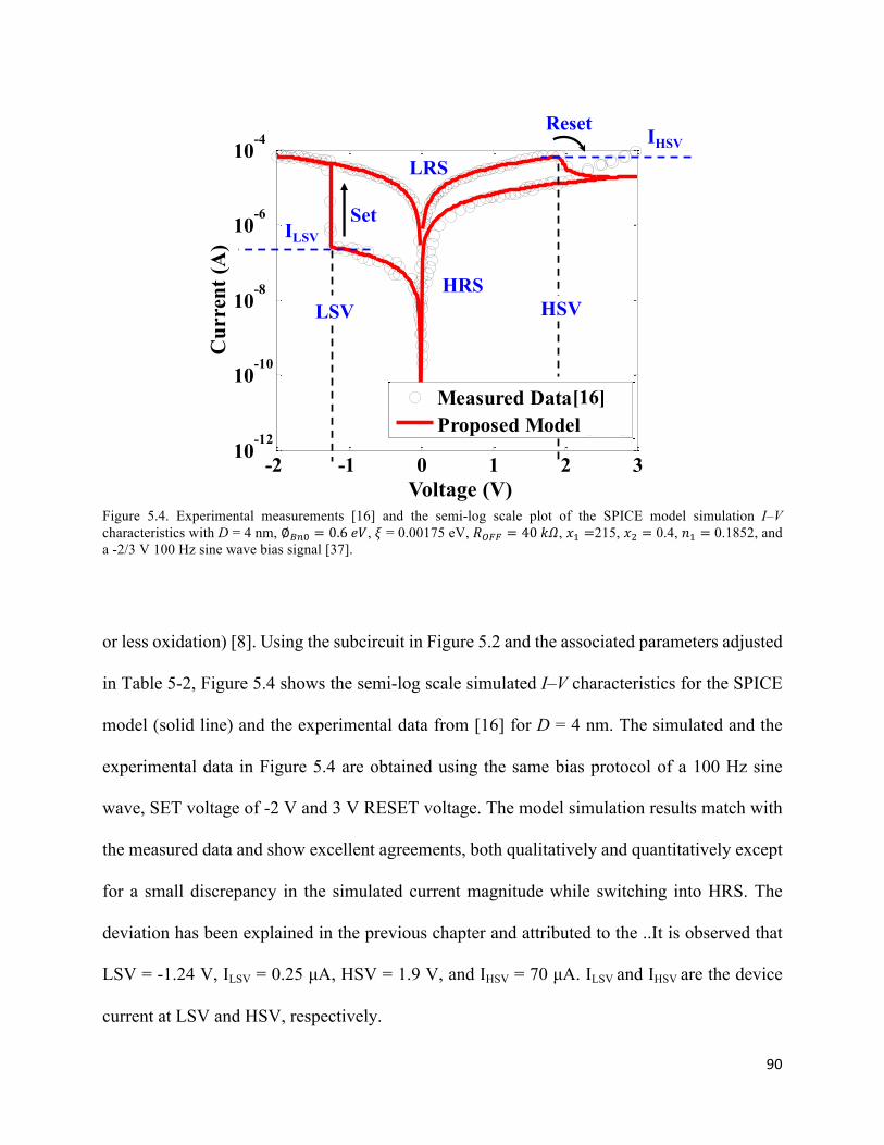
90
Figure 5.4. Experimental measurements [16] and the semi-log scale plot of the SPICE model simulation I–V characteristics with D = 4 nm, ∅XÔx = 0.6𝑒𝑉, 𝜉 = 0.00175 eV, 𝑅V±± = 40𝑘𝛺, 𝑥g =215, 𝑥h = 0.4, 𝑛g = 0.1852, and a -2/3 V 100 Hz sine wave bias signal [37].
or less oxidation) [8]. Using the subcircuit in Figure 5.2 and the associated parameters adjusted
in Table 5-2, Figure 5.4 shows the semi-log scale simulated I–V characteristics for the SPICE
model (solid line) and the experimental data from [16] for D = 4 nm. The simulated and the
experimental data in Figure 5.4 are obtained using the same bias protocol of a 100 Hz sine
wave, SET voltage of -2 V and 3 V RESET voltage. The model simulation results match with
the measured data and show excellent agreements, both qualitatively and quantitatively except
for a small discrepancy in the simulated current magnitude while switching into HRS. The
deviation has been explained in the previous chapter and attributed to the ..It is observed that
LSV = -1.24 V, ILSV = 0.25 µA, HSV = 1.9 V, and IHSV = 70 µA. ILSV and IHSV are the device
current at LSV and HSV, respectively.
-2 -1 0 1 2 310
-12
10-10
10-8
10-6
10-4
Measured DataProposed Model [ ]
Voltage (V)
HSVLSV
Set
LRS
HRS
Cur
rent
(A)
IHSV
ILSV
[16]
Reset
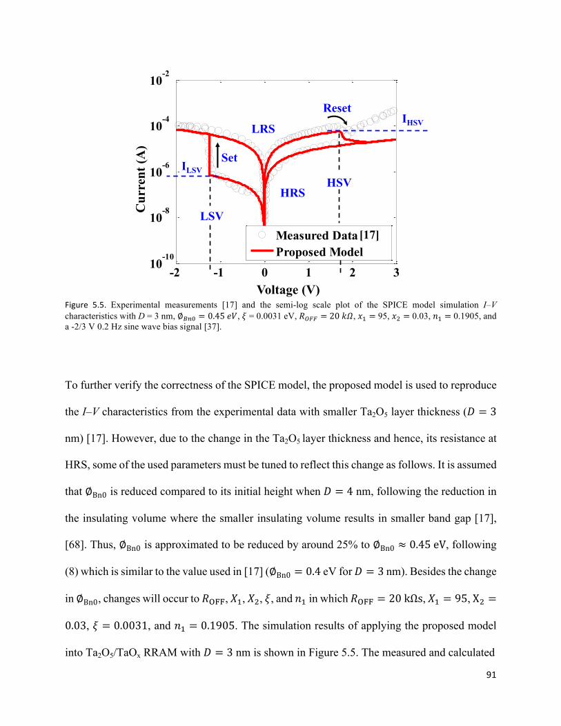
91
Figure 5.5. Experimental measurements [17] and the semi-log scale plot of the SPICE model simulation I–V characteristics with D = 3 nm, ∅XÔx = 0.45𝑒𝑉, 𝜉 = 0.0031 eV, 𝑅V±± = 20𝑘𝛺, 𝑥g = 95, 𝑥h = 0.03, 𝑛g = 0.1905, and a -2/3 V 0.2 Hz sine wave bias signal [37].
To further verify the correctness of the SPICE model, the proposed model is used to reproduce
the I–V characteristics from the experimental data with smaller Ta2O5 layer thickness (𝐷 = 3
nm) [17]. However, due to the change in the Ta2O5 layer thickness and hence, its resistance at
HRS, some of the used parameters must be tuned to reflect this change as follows. It is assumed
that ∅Bn0 is reduced compared to its initial height when 𝐷 = 4 nm, following the reduction in
the insulating volume where the smaller insulating volume results in smaller band gap [17],
[68]. Thus, ∅Bn0 is approximated to be reduced by around 25% to ∅Bn0 ≈ 0.45eV, following
(8) which is similar to the value used in [17] (∅Bn0 = 0.4 eV for 𝐷 = 3 nm). Besides the change
in ∅Bn0, changes will occur to 𝑅GKK, 𝑋g, 𝑋h, 𝜉, and 𝑛g in which 𝑅GKK = 20kΩs, 𝑋g = 95, Xh =
0.03, 𝜉 = 0.0031, and 𝑛g = 0.1905. The simulation results of applying the proposed model
into Ta2O5/TaOx RRAM with 𝐷 = 3 nm is shown in Figure 5.5. The measured and calculated
-2 -1 0 1 2 310
-10
10-8
10-6
10-4
10-2
Measured DataProposed Model [ ]
Voltage (V)
HSV
LSV
LRS
HRS
Cur
rent
(A)
IHSV
ILSVSet
Reset
[17]
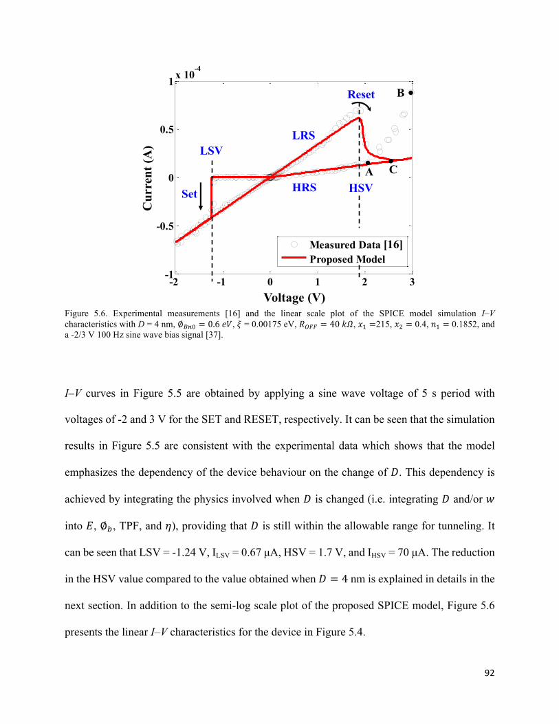
92
Figure 5.6. Experimental measurements [16] and the linear scale plot of the SPICE model simulation I–V characteristics with D = 4 nm, ∅XÔx = 0.6𝑒𝑉, 𝜉 = 0.00175 eV, 𝑅V±± = 40𝑘𝛺, 𝑥g =215, 𝑥h = 0.4, 𝑛g = 0.1852, and a -2/3 V 100 Hz sine wave bias signal [37].
I–V curves in Figure 5.5 are obtained by applying a sine wave voltage of 5 s period with
voltages of -2 and 3 V for the SET and RESET, respectively. It can be seen that the simulation
results in Figure 5.5 are consistent with the experimental data which shows that the model
emphasizes the dependency of the device behaviour on the change of 𝐷. This dependency is
achieved by integrating the physics involved when 𝐷 is changed (i.e. integrating 𝐷 and/or 𝑤
into 𝐸, ∅, TPF, and 𝜂), providing that 𝐷 is still within the allowable range for tunneling. It
can be seen that LSV = -1.24 V, ILSV = 0.67 µA, HSV = 1.7 V, and IHSV = 70 µA. The reduction
in the HSV value compared to the value obtained when 𝐷 = 4 nm is explained in details in the
next section. In addition to the semi-log scale plot of the proposed SPICE model, Figure 5.6
presents the linear I–V characteristics for the device in Figure 5.4.
-2 -1 0 1 2 3-1
-0.5
0
0.5
1 x 10⁻⁴
Measured DataProposed Model
Voltage (V)
HSV
LSV
Set
LRS
HRS
Cur
rent
(A)
[16]
Reset B
A C
.
. .
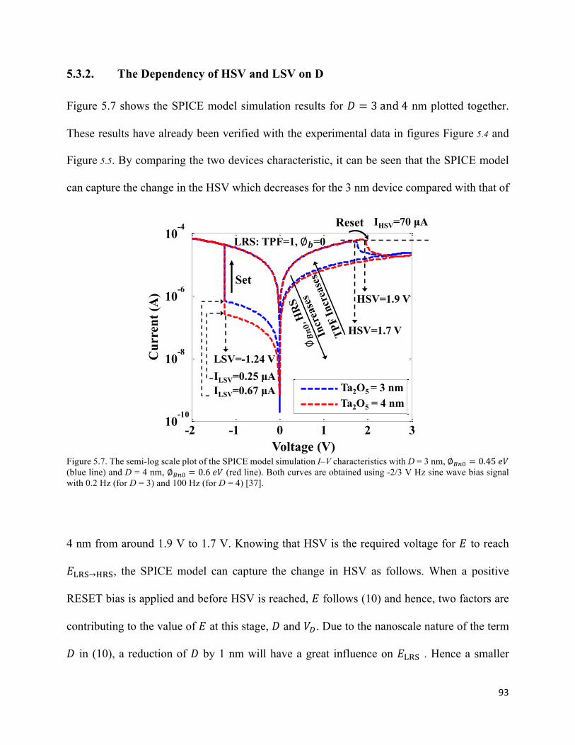
93
5.3.2. The Dependency of HSV and LSV on D
Figure 5.7 shows the SPICE model simulation results for 𝐷 = 3and4 nm plotted together.
These results have already been verified with the experimental data in figures Figure 5.4 and
Figure 5.5. By comparing the two devices characteristic, it can be seen that the SPICE model
can capture the change in the HSV which decreases for the 3 nm device compared with that of
Figure 5.7. The semi-log scale plot of the SPICE model simulation I–V characteristics with D = 3 nm, ∅XÔx = 0.45𝑒𝑉 (blue line) and D = 4 nm, ∅XÔx = 0.6𝑒𝑉 (red line). Both curves are obtained using -2/3 V Hz sine wave bias signal with 0.2 Hz (for D = 3) and 100 Hz (for D = 4) [37].
4 nm from around 1.9 V to 1.7 V. Knowing that HSV is the required voltage for 𝐸 to reach
𝐸¡→, the SPICE model can capture the change in HSV as follows. When a positive
RESET bias is applied and before HSV is reached, 𝐸 follows (10) and hence, two factors are
contributing to the value of 𝐸 at this stage, 𝐷 and 𝑉J. Due to the nanoscale nature of the term
𝐷 in (10), a reduction of 𝐷 by 1 nm will have a great influence on 𝐸¡ . Hence a smaller
-2 -1 0 1 2 310
-10
10-8
10-6
10-4
Voltage (V)
LSV=-1.24 V
LRS: TPF=1, ∅𝒃=0
Cur
rent
(A)
IHSV=70 µA
Ta2O5 = 3 nmTa2O5 = 4 nm
HSV=1.9 V
HSV=1.7 V
ILSV=0.67 µAILSV=0.25 µA
Set
Reset
94
voltage 𝑉 is required to reach 𝐸¡→ when 𝐷 is reduced from 4 to 3 nm, which explain the
smaller HSV obtained in Figure 5.7. It can be seen in Figure 5.7 that during LRS, the parameters
TPF and ∅ maintain their maximum and minimum values (1 and around 0, respectively),
irrespective of the value of 𝐷. Thus, HSV is not affected by these two parameters when 𝐷 is
changed.
𝐸¡ =ORJ
= O`YR#`O²RJ
. (10)
Besides HSV, the SPICE model can also demonstrate the correct LSV when 𝐷 is changed.
According to the experiments in [8], [17], and [16] (see figures Figure 5.4 and Figure 5.5), the
Ta2O5/TaOx RRAM maintains its LSV despite the change in 𝐷. Figure 5.7 shows that the
SPICE model simulation captures this intrinsic feature and show the same LSV when D is
changed from 3 to 4 nm. These results verify that due to the correct modelling of 𝐸 in (2) and
(3), the SPICE model can successfully demonstrate the dependency of HSV and LSV on 𝐷.
5.3.3. The Effects of Changing D on the Values of LRS and HRS
The SPICE model can successfully demonstrate the change in LRS and HRS values when 𝐷
and the value of 𝑅OFF are changed. According to the experiments in [8], [17], and [16] (see
figure. Figure 5.4 and Figure 5.5), the HRS for Ta2O5/TaOx RRAM decreases by decreasing 𝐷
while the LRS is insensitive to the change in 𝐷. Figure 5.7 shows that the SPICE model can
successfully capture this feature where HRS is lowered when 𝐷 is decreased from 4 to 3 nm
whereas LRS remains unchanged. The SPICE model can predict this intrinsic phenomenon as
follows.
95
HRS: While at HRS, the device resistance is determined by 𝑅X + 𝑅GKK + 𝑉/𝐼 [21]. The
interface resistance 𝑉/𝐼 at HRS is influenced by TPF and ∅. At HRS, TPF and ∅ are
proportional to 𝑤 = 𝐷[(6) and (8)] where decreasing 𝐷 results in larger and smaller values of
TPF and ∅ (∅®¯x is smaller), respectively. As a result, 𝐼 is increased according to (6) and the
interface voltage 𝑉 is decreased (5). Consequently, the resistance 𝑉/𝐼 is reduced for smaller
𝐷. Besides 𝑉/𝐼, 𝑅GKK is also reduced for smaller 𝐷 (due to the smaller insulating volume). It
is found that 𝑅GKK = 20kΩs provides the best fitting to the experimental results when 𝐷 = 3
nm. Therefore, the reduction in 𝑉/𝐼and 𝑅GKK when 𝐷 is reduced leads to smaller HRS.
However, the resistance 𝑅X is insensitive to the change in 𝐷.
LRS: Following the same explanation for HRS, the device resistance at LRS is determined by:
𝑅X + 𝑅GH + 𝑉/𝐼. TPF and ∅ at LRS have the values of 1 and around 0, respectively,
regardless of the value of 𝐷 (see Figure 5.7) which makes the resistance 𝑉/𝐼 at LRS insensitive
to these two parameters (𝑉/𝐼 reaches its minimum value at LRS). Also, 𝑅X and 𝑅GH are
selected to satisfy the condition 𝑅X ≫ 𝑅GH as in [1]. Hence, the small change in 𝑅GH due to
the change of 𝐷 is negligible (𝑅GH is assumed to be fixed in the SPICE model) and the total
current while at LRS is limited by the relatively large 𝑅X. This explains why the change in 𝐷
has no effect on the LRS. These results show that by integrating TPF and ∅, the proposed
SPICE model can manifest the dependency of LRS and HRS on D.
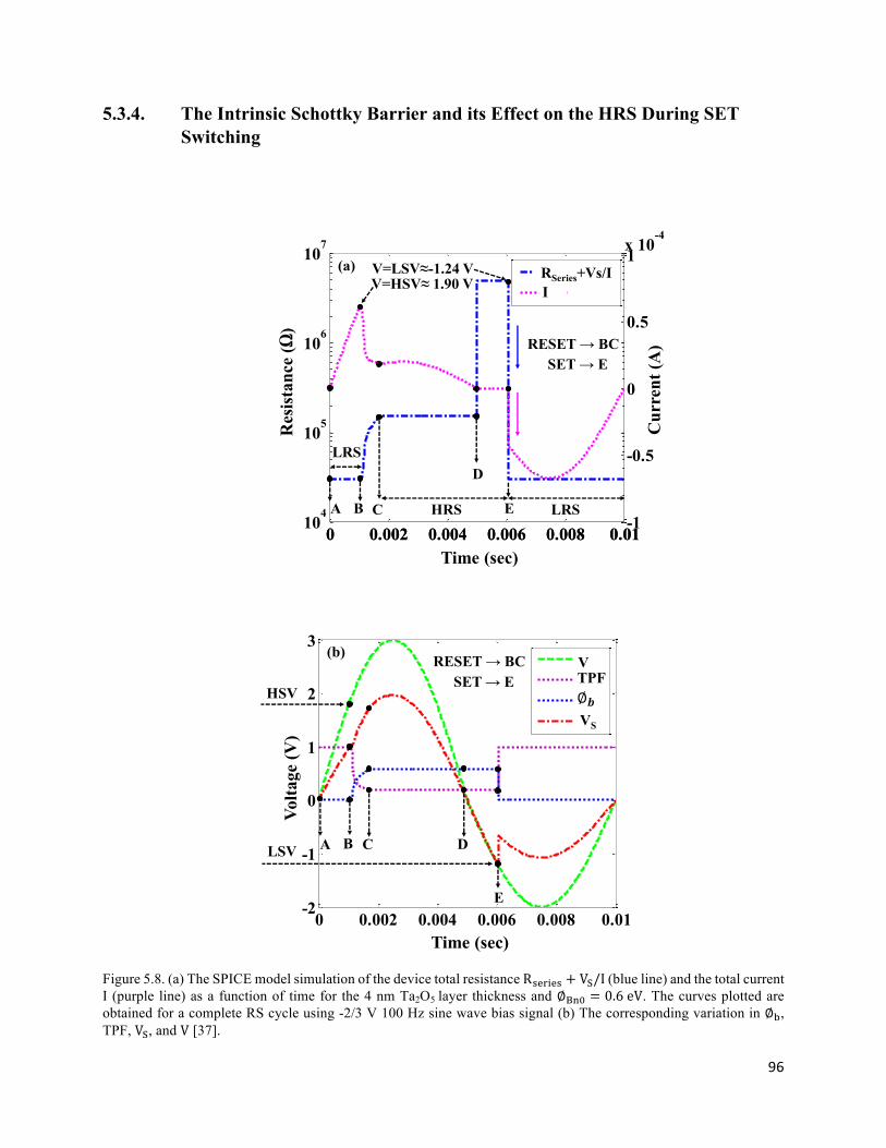
96
5.3.4. The Intrinsic Schottky Barrier and its Effect on the HRS During SET Switching
Figure 5.8. (a) The SPICE model simulation of the device total resistance R + V/I (blue line) and the total current I (purple line) as a function of time for the 4 nm Ta2O5 layer thickness and ∅®¯x = 0.6eV. The curves plotted are obtained for a complete RS cycle using -2/3 V 100 Hz sine wave bias signal (b) The corresponding variation in ∅&, TPF, V, and V [37].
0 0.002 0.004 0.006 0.008 0.01-2
-1
0
1
2
3
∅𝒃
B CA
Time (sec)
Volta
ge (V
)
HSVSET → E
LSV
VTPF
VS
D
RESET → BC
E
(b)
0 0.002 0.004 0.006 0.008 0.0110
4
105
106
107
0 0.002 0.004 0.006 0.008 0.01-1
-0.5
0
0.5
1x 10⁻⁴
Time (sec)
Res
ista
nce
(Ω)
Cur
rent
(A)
IRSeries+Vs/I
BA C
D
E LRSHRS
LRS
V=HSV≈ 1.90 VV=LSV≈-1.24 V
SET → ERESET → BC
(a)
97
Using the proposed SPICE model, a comprehensive analysis and simulation of Schottky-like
tunnelling interface (Pt/Ta2O5) reveal that the device resistance during HRS is not fixed, but
depends on the bias polarity.
Figure 5.8(a) shows the simulated device resistance 𝑅 + 𝑉/𝐼 and the current 𝐼 as a
function of time for 𝐷 = 4 nm for a complete RS cycle while
Figure 5.8(b) compares the corresponding variation in ∅, TPF, 𝑉, and 𝑉. Assuming LRS as
the initial state (point A), it can be seen that the device first starts switching into HRS when
HSV=1.9 V is reached (point B). The device reaches its HRS at the end of the switching period
(end of BC). However, the imperative remark that can be observed is that once a negative SET
bias is applied (point D), the resistance switches from few hundreds of Kilo Ohms (HRS value)
to few Mega Ohms and the current tends to align with 0 A. The device maintains this very high
resistance until LSV=-1.24 V is reached (point E) where the resistance drops significantly and
an abrupt increase in the current is observed, indicating LRS. This behaviour is attributed to
the coexistence of the reversed-biased Schottky barrier associated with TPF as explained next.
The device current is determined by the multiplication of three terms T1, T2, and TPF as
follows:
𝐼 = 𝐴𝐴∗𝑇xhexp`(∅Ö)/Oczg
exp³²¾³c − 1
zh
exp`gxlw× µI
z±
. (11)
1) While at LRS (AB), 𝐼 is mainly influenced by T2 and varies according to 𝑉. TPF equals 1
and has no effect on suppressing 𝐼 at LRS (no tunneling current). Similarly, ∅ ≈ 0 at LRS
(ohmic contact) and T1 is fixed at its maximum value and does not reduce 𝐼. 2) Overtime, HSV
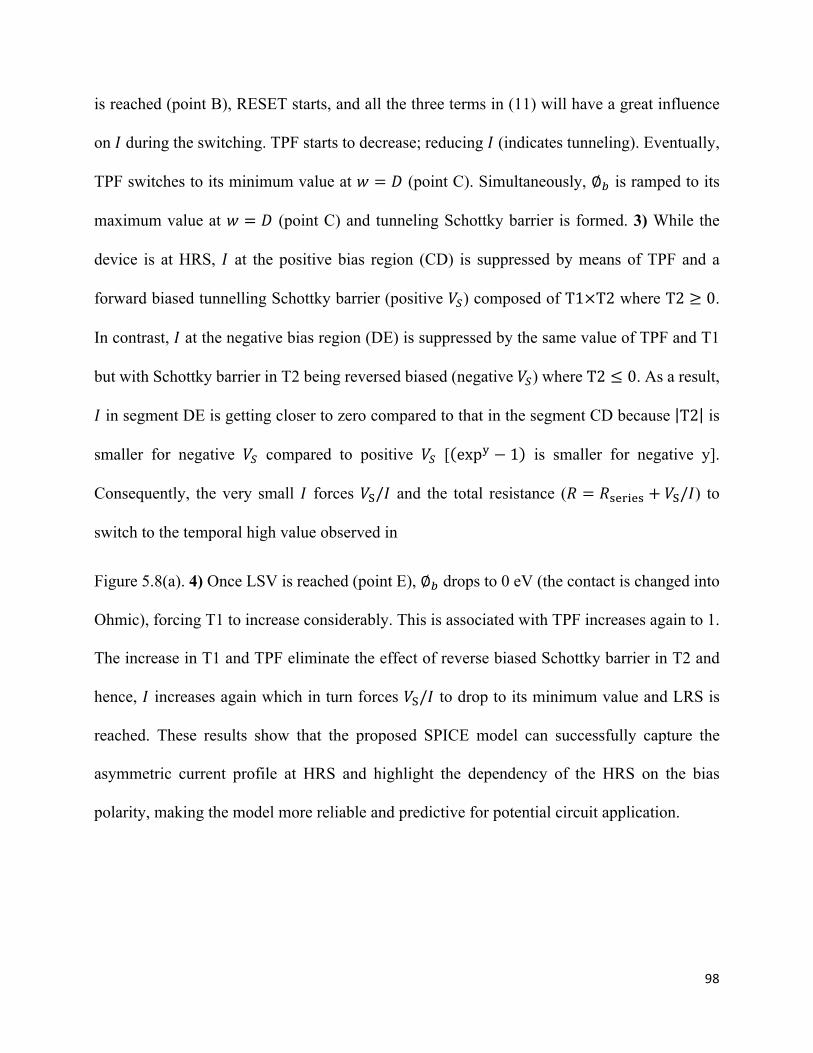
98
is reached (point B), RESET starts, and all the three terms in (11) will have a great influence
on 𝐼 during the switching. TPF starts to decrease; reducing 𝐼 (indicates tunneling). Eventually,
TPF switches to its minimum value at 𝑤 = 𝐷 (point C). Simultaneously, ∅ is ramped to its
maximum value at 𝑤 = 𝐷 (point C) and tunneling Schottky barrier is formed. 3) While the
device is at HRS, 𝐼 at the positive bias region (CD) is suppressed by means of TPF and a
forward biased tunnelling Schottky barrier (positive 𝑉) composed of T1×T2 where T2 ≥ 0.
In contrast, 𝐼 at the negative bias region (DE) is suppressed by the same value of TPF and T1
but with Schottky barrier in T2 being reversed biased (negative 𝑉) where T2 ≤ 0. As a result,
𝐼 in segment DE is getting closer to zero compared to that in the segment CD because T2 is
smaller for negative 𝑉 compared to positive 𝑉 [ exp( − 1 is smaller for negative y].
Consequently, the very small 𝐼 forces 𝑉/𝐼 and the total resistance (𝑅 = 𝑅 + 𝑉/𝐼) to
switch to the temporal high value observed in
Figure 5.8(a). 4) Once LSV is reached (point E), ∅ drops to 0 eV (the contact is changed into
Ohmic), forcing T1 to increase considerably. This is associated with TPF increases again to 1.
The increase in T1 and TPF eliminate the effect of reverse biased Schottky barrier in T2 and
hence, 𝐼 increases again which in turn forces 𝑉/𝐼 to drop to its minimum value and LRS is
reached. These results show that the proposed SPICE model can successfully capture the
asymmetric current profile at HRS and highlight the dependency of the HRS on the bias
polarity, making the model more reliable and predictive for potential circuit application.
99
5.3.5. Testing the Model under Different Types of Input Signals
The use of the conventional voltage quantities (e.g. sinusoidal, rectangular, and triangular
waveforms) is common in many potential memory applications. Therefore, in order to increase
the number of the bi-layered RRAM-based circuit applications, a SPICE model that has a stable
behaviour (same levels of LRS and HRS) under changing its input stimulus type is essential
(providing the input signal is large enough to provide the required LSV and HSV). After the
proposed SPICE model matches the experimental results for a sinusoidal signal, it is tested
under the same -2 V SET and 3 V RESET voltages but for a triangular and rectangular signals
Figure 5.9. The SPICE model simulation of the device total resistance 𝑅ÇïïÇ + 𝑉/𝐼 (blue line) and the applied voltage 𝑉 (red dashed line) as a function of time for D = 4 nm. The curves plotted are obtained for a complete RS cycle using
0 0.002 0.004 0.006 0.008 0.01104
105
106
107
0 0.002 0.004 0.006 0.008 0.01-2
-1
0
1
2
3
Time (sec)
Res
ista
nce
(Ω)
Volta
ge (V
)
VRSeries+Vs/I
LRS
HRSLRS
SET
RESET
(a)
𝑫 = 𝟒𝐧𝐦HSV≈ 1.90 V
LSV≈ -1.24 V
0 2 4 6 8 10x 10-3
104
105
106
107
0 2 4 6 8 10x 10-3
-2
0
2
4
Time (sec)
Res
ista
nce
(Ω)
Volta
ge (V
)
LRS
SET
RESET
(b)
𝑫 = 𝟒𝐧𝐦
0 0.002 0.004 0.006 0.008 0.01104
105
106
107
0 0.002 0.004 0.006 0.008 0.01-2
-1
0
1
2
3
HRS
0 0.002 0.004 0.006 0.008 0.01104
105
106
107
0 0.002 0.004 0.006 0.008 0.01-2
-1
0
1
2
3RSeries+Vs/IV
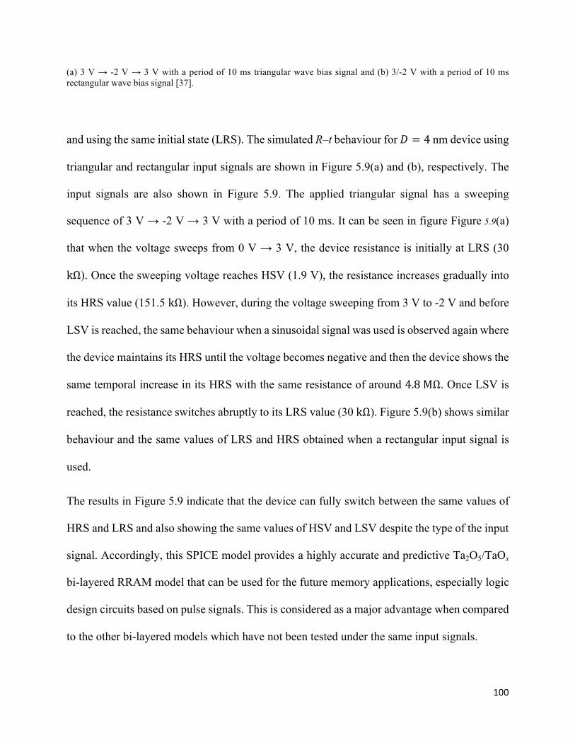
100
(a) 3 V → -2 V → 3 V with a period of 10 ms triangular wave bias signal and (b) 3/-2 V with a period of 10 ms rectangular wave bias signal [37].
and using the same initial state (LRS). The simulated R–t behaviour for 𝐷 = 4 nm device using
triangular and rectangular input signals are shown in Figure 5.9(a) and (b), respectively. The
input signals are also shown in Figure 5.9. The applied triangular signal has a sweeping
sequence of 3 V → -2 V → 3 V with a period of 10 ms. It can be seen in figure Figure 5.9(a)
that when the voltage sweeps from 0 V → 3 V, the device resistance is initially at LRS (30
kΩ). Once the sweeping voltage reaches HSV (1.9 V), the resistance increases gradually into
its HRS value (151.5 kΩ). However, during the voltage sweeping from 3 V to -2 V and before
LSV is reached, the same behaviour when a sinusoidal signal was used is observed again where
the device maintains its HRS until the voltage becomes negative and then the device shows the
same temporal increase in its HRS with the same resistance of around 4.8MΩ. Once LSV is
reached, the resistance switches abruptly to its LRS value (30 kΩ). Figure 5.9(b) shows similar
behaviour and the same values of LRS and HRS obtained when a rectangular input signal is
used.
The results in Figure 5.9 indicate that the device can fully switch between the same values of
HRS and LRS and also showing the same values of HSV and LSV despite the type of the input
signal. Accordingly, this SPICE model provides a highly accurate and predictive Ta2O5/TaOx
bi-layered RRAM model that can be used for the future memory applications, especially logic
design circuits based on pulse signals. This is considered as a major advantage when compared
to the other bi-layered models which have not been tested under the same input signals.
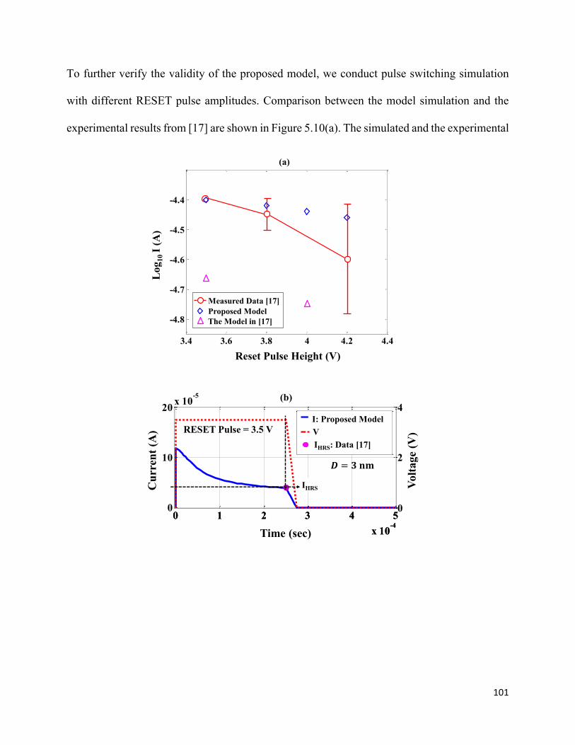
101
To further verify the validity of the proposed model, we conduct pulse switching simulation
with different RESET pulse amplitudes. Comparison between the model simulation and the
experimental results from [17] are shown in Figure 5.10(a). The simulated and the experimental
Reset Pulse Height (V)
Log
10 I
(A)
3.4 3.6 3.8 4 4.2 4.4
-4.8
-4.7
-4.6
-4.5
-4.4
Measured Data [17]Proposed ModelThe Model in [17]
(a)
0 1 2 3 4 5x 10⁻⁴
0
10
20 x 10-5
0 1 2 3 4 5x 10⁻⁴
0
2
4
Time (sec)
Cur
rent
(A)
Volta
ge (V
)RESET Pulse = 3.5 V
(b)
𝑫 = 𝟑𝐧𝐦
0 0.002 0.004 0.006 0.008 0.01104
105
106
107
0 0.002 0.004 0.006 0.008 0.01-2
-1
0
1
2
3I: Proposed ModelVIHRS: Data [17]
IHRS
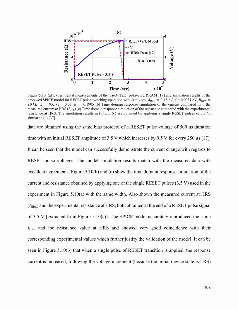
102
Figure 5.10. (a) Experimental measurements of the Ta2O5/TaOx bi-layered RRAM [17] and simulation results of the proposed SPICE model for RESET pulse switching operation with D = 3 nm, ∅XÔx = 0.45𝑒𝑉, 𝜉 = 0.0031 eV, 𝑅V±± = 20𝑘𝛺, 𝑥g = 95, 𝑥h = 0.03, 𝑛g = 0.1905 (b) Time domain response simulation of the current compared with the measured current at HRS (IHRS) (c) Time domain response simulation of the resistance compared with the experimental resistance at HRS. The simulation results in (b) and (c) are obtained by applying a single RESET pulses of 3.5 V, similar to (a) [37].
data are obtained using the same bias protocol of a RESET pulse voltage of 500 ns duration
time with an initial RESET amplitude of 3.5 V which increases by 0.5 V for every 250 µs [17].
It can be seen that the model can successfully demonstrate the current change with regards to
RESET pulse voltages. The model simulation results match with the measured data with
excellent agreements. Figure 5.10(b) and (c) show the time domain response simulation of the
current and resistance obtained by applying one of the single RESET pulses (3.5 V) used in the
experiment in Figure 5.10(a) with the same width. Also shown the measured current at HRS
(IHRS) and the experimental resistance at HRS, both obtained at the end of a RESET pulse signal
of 3.5 V [extracted from Figure 5.10(a)]. The SPICE model accurately reproduced the same
IHRS and the resistance value at HRS and showed very good coincidence with their
corresponding experimental values which further justify the validation of the model. It can be
seen in Figure 5.10(b) that when a single pulse of RESET transition is applied, the response
current is increased, following the voltage increment (because the initial device state is LRS)
0 1 2 3 4 5x 10⁻⁴
0
5
10 x 104
0 1 2 3 4 5x 10⁻⁴
0
2
4
Time (sec)
Res
ista
nce
(Ω)
Volta
ge (V
)
(c)
𝑫 = 𝟑𝐧𝐦
0 0.002 0.004 0.006 0.008 0.01104
105
106
107
0 0.002 0.004 0.006 0.008 0.01-2
-1
0
1
2
3RSeries+Vs/I: Model
VHRS: Data [17]
HRS
RESET Pulse = 3.5 V
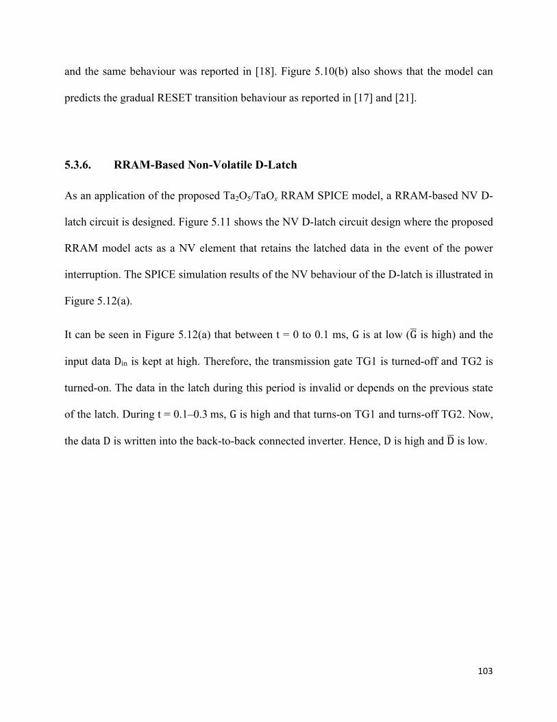
103
and the same behaviour was reported in [18]. Figure 5.10(b) also shows that the model can
predicts the gradual RESET transition behaviour as reported in [17] and [21].
5.3.6. RRAM-Based Non-Volatile D-Latch
As an application of the proposed Ta2O5/TaOx RRAM SPICE model, a RRAM-based NV D-
latch circuit is designed. Figure 5.11 shows the NV D-latch circuit design where the proposed
RRAM model acts as a NV element that retains the latched data in the event of the power
interruption. The SPICE simulation results of the NV behaviour of the D-latch is illustrated in
Figure 5.12(a).
It can be seen in Figure 5.12(a) that between t = 0 to 0.1 ms, G is at low (G is high) and the
input data Din is kept at high. Therefore, the transmission gate TG1 is turned-off and TG2 is
turned-on. The data in the latch during this period is invalid or depends on the previous state
of the latch. During t = 0.1–0.3ms, G is high and that turns-on TG1 and turns-off TG2. Now,
the data D is written into the back-to-back connected inverter. Hence, D is high and D is low.
104
Figure 5.11. Schematic of the RRAM-based NV D-Latch with the Ta2O5/TaOx RRAM SPICE model integrated [37].
At the same duration, the data is also written into the RRAM. It can be observed from the
simulation results in Figure 5.12(a) that the current I flowing through the RRAM decreases
from 80 µA (at 0.1 ms) to 18 µA (at 0.3 ms) and this is due to the resistance of the RRAM
which is initially at LRS and then changes to HRS. At t = 0.3 ms, G goes to low, hence, TG2
is turned-on and TG1 is turned-off. This retains the data in the latch and the HRS in the RRAM.
When a power interruption occurs at t = 0.4 ms (VDD = 0 V), it can be observed that D, D, and
the current through the RRAM are low. Then at t = 0.42 ms, when the power resumes (VDD =
3 V), the current through the high resistance RRAM (18 µA), retains the original value of D (to
high) and D (to low). Thus, the data is successfully retained in the latch.
Ta2O5TaOx
VDD
𝐃$
RRAM
𝐆$
𝐆$
I
TG1
VDD
𝐃𝐃𝐆
𝐆
𝐃in
TG2
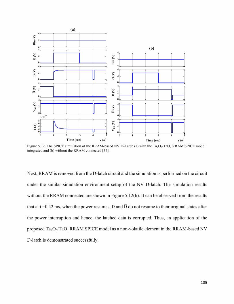
105
Figure 5.12. The SPICE simulation of the RRAM-based NV D-Latch (a) with the Ta2O5/TaOx RRAM SPICE model integrated and (b) without the RRAM connected [37].
Next, RRAM is removed from the D-latch circuit and the simulation is performed on the circuit
under the similar simulation environment setup of the NV D-latch. The simulation results
without the RRAM connected are shown in Figure 5.12(b). It can be observed from the results
that at t =0.42 ms, when the power resumes, D and D do not resume to their original states after
the power interruption and hence, the latched data is corrupted. Thus, an application of the
proposed Ta2O5/TaOx RRAM SPICE model as a non-volatile element in the RRAM-based NV
D-latch is demonstrated successfully.
0 0.2 0.4 0.6 0.8 1
x 10-3
2
3
4
0 1 2 3 4 5
x 10-4
0
2
4
0 1 2 3 4 5
x 10-4
0
2
4
0 1 2 3 4 5
x 10-4
0
2
4
0 1 2 3 4 5
x 10-4
0
2
4
0 1 2 3 4 5
x 10-4
02468
x 10-5
0 0.2 0.4 0.6 0.8 1
x 10-3
2
3
4
0 1 2 3 4 5
x 10-4
0
2
4
0 1 2 3 4 5
x 10-4
0
2
4
0 1 2 3 4 5
x 10-4
0
2
4
0 1 2 3 4 5
x 10-4
0
2
4
0 1 2 3 4 5
x 10-4
02468
x 10-5
0 0.2 0.4 0.6 0.8 1
x 10-3
2
3
4
0 1 2 3 4 5
x 10-4
0
2
4
0 1 2 3 4 5
x 10-4
0
2
4
0 1 2 3 4 5
x 10-4
0
2
4
0 1 2 3 4 5
x 10-4
0
2
4
0 1 2 3 4 5
x 10-4
02468
x 10-5
0 0.2 0.4 0.6 0.8 1
x 10-3
2
3
4
0 1 2 3 4 5
x 10-4
0
2
4
0 1 2 3 4 5
x 10-4
0
2
4
0 1 2 3 4 5
x 10-4
0
2
4
0 1 2 3 4 5
x 10-4
0
2
4
0 1 2 3 4 5
x 10-4
02468
x 10-5
0 0.2 0.4 0.6 0.8 1
x 10-3
2
3
4
0 1 2 3 4 5
x 10-4
0
2
4
0 1 2 3 4 5
x 10-4
0
2
4
0 1 2 3 4 5
x 10-4
0
2
4
0 1 2 3 4 5
x 10-4
0
2
4
0 1 2 3 4 5
x 10-4
02468
x 10-5
0 0.2 0.4 0.6 0.8 1
x 10-3
2
3
4
0 1 2 3 4 5
x 10-4
0
2
4
0 1 2 3 4 5
x 10-4
0
2
4
0 1 2 3 4 5
x 10-4
0
2
4
0 1 2 3 4 5
x 10-4
0
2
4
0 1 2 3 4 5
x 10-4
02468
x 10-5
I (A
)D
in (V
)
Time (sec)
G (V
)D
(V)
𝐃"(V
)V
DD
(V)
(a)
0 1 2 3 4 5
x 10-4
2
3
4
0 1 2 3 4 5
x 10-4
0
2
4
0 1 2 3 4 5
x 10-4
0
2
4
0 1 2 3 4 5
x 10-4
0
1
2
0 1 2 3 4 5
x 10-4
0
2
4
0 1 2 3 4 5
x 10-4
2
3
4
0 1 2 3 4 5
x 10-4
0
2
4
0 1 2 3 4 5
x 10-4
0
2
4
0 1 2 3 4 5
x 10-4
0
1
2
0 1 2 3 4 5
x 10-4
0
2
4
0 1 2 3 4 5
x 10-4
2
3
4
0 1 2 3 4 5
x 10-4
0
2
4
0 1 2 3 4 5
x 10-4
0
2
4
0 1 2 3 4 5
x 10-4
0
1
2
0 1 2 3 4 5
x 10-4
0
2
4
0 1 2 3 4 5
x 10-4
2
3
4
0 1 2 3 4 5
x 10-4
0
2
4
0 1 2 3 4 5
x 10-4
0
2
4
0 1 2 3 4 5
x 10-4
0
1
2
0 1 2 3 4 5
x 10-4
0
2
4
0 1 2 3 4 5
x 10-4
2
3
4
0 1 2 3 4 5
x 10-4
0
2
4
0 1 2 3 4 5
x 10-4
0
2
4
0 1 2 3 4 5
x 10-4
0
1
2
0 1 2 3 4 5
x 10-4
0
2
4
Din
(V)
Time (sec)
G (V
)D
(V)
𝐃"(V
)V
DD
(V)
(b)
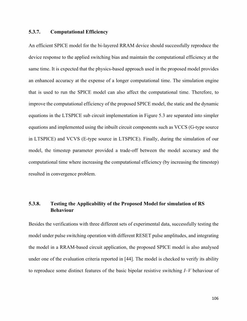
106
5.3.7. Computational Efficiency
An efficient SPICE model for the bi-layered RRAM device should successfully reproduce the
device response to the applied switching bias and maintain the computational efficiency at the
same time. It is expected that the physics-based approach used in the proposed model provides
an enhanced accuracy at the expense of a longer computational time. The simulation engine
that is used to run the SPICE model can also affect the computational time. Therefore, to
improve the computational efficiency of the proposed SPICE model, the static and the dynamic
equations in the LTSPICE sub circuit implementation in Figure 5.3 are separated into simpler
equations and implemented using the inbuilt circuit components such as VCCS (G-type source
in LTSPICE) and VCVS (E-type source in LTSPICE). Finally, during the simulation of our
model, the timestep parameter provided a trade-off between the model accuracy and the
computational time where increasing the computational efficiency (by increasing the timestep)
resulted in convergence problem.
5.3.8. Testing the Applicability of the Proposed Model for simulation of RS Behaviour
Besides the verifications with three different sets of experimental data, successfully testing the
model under pulse switching operation with different RESET pulse amplitudes, and integrating
the model in a RRAM-based circuit application, the proposed SPICE model is also analysed
under one of the evaluation criteria reported in [44]. The model is checked to verify its ability
to reproduce some distinct features of the basic bipolar resistive switching I–V behaviour of
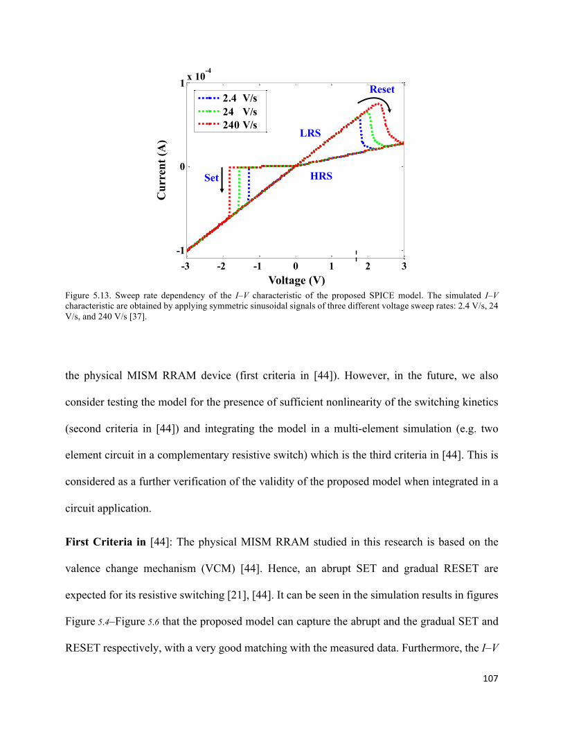
107
Figure 5.13. Sweep rate dependency of the I–V characteristic of the proposed SPICE model. The simulated I–V characteristic are obtained by applying symmetric sinusoidal signals of three different voltage sweep rates: 2.4 V/s, 24 V/s, and 240 V/s [37].
the physical MISM RRAM device (first criteria in [44]). However, in the future, we also
consider testing the model for the presence of sufficient nonlinearity of the switching kinetics
(second criteria in [44]) and integrating the model in a multi-element simulation (e.g. two
element circuit in a complementary resistive switch) which is the third criteria in [44]. This is
considered as a further verification of the validity of the proposed model when integrated in a
circuit application.
First Criteria in [44]: The physical MISM RRAM studied in this research is based on the
valence change mechanism (VCM) [44]. Hence, an abrupt SET and gradual RESET are
expected for its resistive switching [21], [44]. It can be seen in the simulation results in figures
Figure 5.4–Figure 5.6 that the proposed model can capture the abrupt and the gradual SET and
RESET respectively, with a very good matching with the measured data. Furthermore, the I–V
-3 -2 -1 0 1 2 3-1
0
1 x 10⁻⁴
2.4 V/s24 V/s240 V/s
Voltage (V)
Set
LRS
HRSC
urre
nt (A
)
Reset
108
characteristics of the physical MISM RRAM are asymmetric with respect to the origin which
can also be successfully reproduced by the proposed model (See figures Figure 5.4–Figure 5.6).
The model can also demonstrate the general trend of a higher SET and RESET voltages for
increasing voltage sweep rate as reported in [44]. Figure 5.13 shows the simulation results
achieved by applying three symmetric sinusoidal signals with different sweep rates of 2.4, 24,
and 240 V/s. The obtained simulation results show that the model depicts higher SET and
RESET voltage for increasing sweep rate, in agreement with the previous results of VCM [44].
109
6. Chapter Six: A Predictive Compact SPICE Model of TaOx-Based MIM RRAM
A PREDECTIVE COMPACT SPICE MODEL OF
TaOx-BASED MIM RRAM
Summary
Among the available RS materials, Tantalum oxide demonstrated encouraging RS behaviour
and properties. As mentioned in this thesis report, this material showed favourable endurance,
RS speed, multilevel property, and stable phases. However, in order to have a complete library
for a Tantalum-oxide-based RRAM SPICE models, an MIM RRAM SPICE model is also
required besides the MISM RRAM model developed in chapter 5. In this chapter, a predictive
compact MIM SPICE model for RS in Tantalum-oxide-based RRAM is developed. The
proposed compact model is developed based on the analytical predictive MIM model of
Pt/TaOx/Ta RRAM in [42] which is compatible with SPICE. Although this model is not based
on all the physics involved in the device RS and current conduction mechanisms (like the bi-
layered RRAM model developed in this thesis report), it is considered an important first step
toward understanding the physical insight behind these mechanisms.
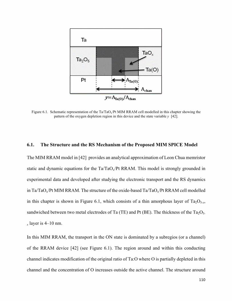
110
Figure 6.1. Schematic representation of the Ta/TaOx/Pt MIM RRAM cell modelled in this chapter showing the pattern of the oxygen depletion region in this device and the state variable y [42].
6.1. The Structure and the RS Mechanism of the Proposed MIM SPICE Model
The MIM RRAM model in [42] provides an analytical approximation of Leon Chua memristor
static and dynamic equations for the Ta/TaOx/Pt RRAM. This model is strongly grounded in
experimental data and developed after studying the electronic transport and the RS dynamics
in Ta/TaOx/Pt MIM RRAM. The structure of the oxide-based Ta/TaOx/Pt RRAM cell modelled
in this chapter is shown in Figure 6.1, which consists of a thin amorphous layer of Ta2O5-x,
sandwiched between two metal electrodes of Ta (TE) and Pt (BE). The thickness of the Ta2O5-
x layer is 4–10 nm.
In this MIM RRAM, the transport in the ON state is dominated by a subregios (or a channel)
of the RRAM device [42] (see Figure 6.1). The region around and within this conducting
channel indicates modification of the original ratio of Ta:O where O is partially depleted in this
channel and the concentration of O increases outside the active channel. The structure around
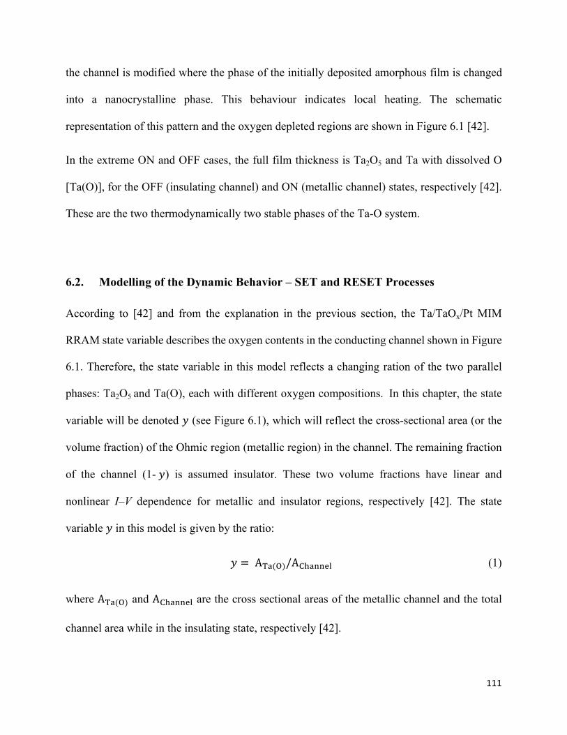
111
the channel is modified where the phase of the initially deposited amorphous film is changed
into a nanocrystalline phase. This behaviour indicates local heating. The schematic
representation of this pattern and the oxygen depleted regions are shown in Figure 6.1 [42].
In the extreme ON and OFF cases, the full film thickness is Ta2O5 and Ta with dissolved O
[Ta(O)], for the OFF (insulating channel) and ON (metallic channel) states, respectively [42].
These are the two thermodynamically two stable phases of the Ta-O system.
6.2. Modelling of the Dynamic Behavior – SET and RESET Processes
According to [42] and from the explanation in the previous section, the Ta/TaOx/Pt MIM
RRAM state variable describes the oxygen contents in the conducting channel shown in Figure
6.1. Therefore, the state variable in this model reflects a changing ration of the two parallel
phases: Ta2O5 and Ta(O), each with different oxygen compositions. In this chapter, the state
variable will be denoted 𝑦 (see Figure 6.1), which will reflect the cross-sectional area (or the
volume fraction) of the Ohmic region (metallic region) in the channel. The remaining fraction
of the channel (1-𝑦) is assumed insulator. These two volume fractions have linear and
nonlinear I–V dependence for metallic and insulator regions, respectively [42]. The state
variable 𝑦 in this model is given by the ratio:
𝑦 = A¥§(G)/A+ا¯¯, (1)
where A¥§(G) and A+ا¯¯, are the cross sectional areas of the metallic channel and the total
channel area while in the insulating state, respectively [42].
112
The RESET switching in this MIM RRAM is obtained by applying negative bias on TE. The
RESET switching dynamics showed best fitting when an exponential voltage-controlled
switching behaviour is used. It also showed additional dependence on the power (Joule heating
effect) which slow down the RESET process. The RESET switching dynamic model used in
[42] is given by equation (2) which showed best fitting to the experimental data.
P-PQ= 𝐴 ∙ sinh O
.S∙ exp[− -S
-
h] ∙ exp[1/(1 + (1 + 𝛽𝑝)](V < 0) (2)
where 𝐴, 𝜎GKK, 𝑦GKK, and 𝛽 are fitting parameters. The value of these parameters are provided
in Table 6-1. 𝑝 is the power which shows that Joule heating slow down RESET process. The
SET switching dynamics of the Ta/TaOx/Pt MIM RRAM in [42] is given by the following
equation [42]:
P-PQ= 𝐵 ∙ sinh O
.ST∙ exp[− -
-ST
h] ∙ exp[𝑝/𝜎2](V < 0) (3)
where 𝐵, 𝜎GH, 𝑦GH, and 𝜎2 are fitting parameters.
The value of these parameters are provided in Table 6-1. It can be seem that the SET process
has opposite dependence on the power 𝑝 when compared to the RESET process where Joule
heating speeds up the SET process. Although this equation showed good agreement with the
experimental data when the applied voltage is above the threshold voltage, it resulted in an
inadequate results at the near-threshold voltage (around 0.5 V) [42].
By comparing equations (2) and (3), it can be seen that the SET and RESET switching
dynamics have the same form of voltage dependence [42]. Both have an exponential
dependence on the applied voltage where a very small increase in the applied voltage results in
113
orders of magnitude faster switching process, which is in agreement with the characteristics of
the Tantalum-Oxide RRAM [42].
6.3. Modelling of the Static Behavior – Current Conduction Process
According to [42], the conduction during LRS for this MIM RRAM model is metallic whereas
the conduction during HRS showed good fitting using the nonlinear Frenkel-Poole equation
[42]. The conduction equation of the device in Figure 6.1 is giving be the following equation
[42]:
𝐼 = 𝑉[𝑦𝐺4 + (1 − 𝑦)𝑎 ∙ exp(𝑏 𝑉 )] (4)
where 𝐼 is the current through the device, 𝑉 is the total voltage across the RRAM device, 𝑎, 𝑏,
and 𝐺4 are constants depends on the material of the conduction channel and can be used a
fitting parameters in the SPICE model. These constants are fixed for a particular cell despite of
its state.
The expression [𝑦𝐺4 + (1 − 𝑦)𝑎 ∙ exp(𝑏 𝑣 )] represents the parallel combination of the two
phases shown in Figure 6.1. When a positive voltage is applied on TE (SET switching), the
linear metallic phase Ta(O) fills the channel (A¥§ G = A+ا¯¯,) and the state variable 𝑦
reaches 1. Hence, from equation (4), the conductance of the RRAM become 𝐺4. Conversely,
when a negative voltage is applied on TE (RESET process), the device reaches its HRS when
the insulating oxide fills the entire channel (A¥§ G = 0) and state variable 𝑦 become 0. As a
results, the conductance in equation (4) become 𝑎 ∙ exp(𝑏 𝑣 ) which describes the nonlinear
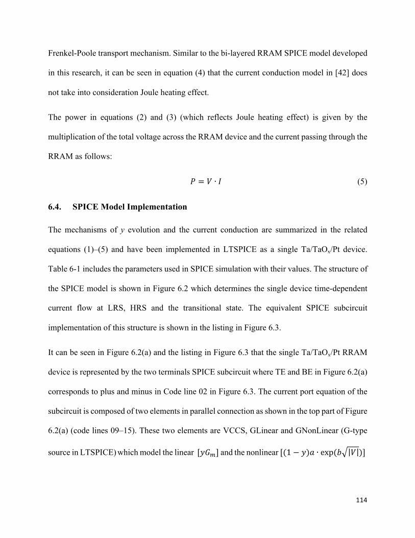
114
Frenkel-Poole transport mechanism. Similar to the bi-layered RRAM SPICE model developed
in this research, it can be seen in equation (4) that the current conduction model in [42] does
not take into consideration Joule heating effect.
The power in equations (2) and (3) (which reflects Joule heating effect) is given by the
multiplication of the total voltage across the RRAM device and the current passing through the
RRAM as follows:
𝑃 = 𝑉 ∙ 𝐼 (5)
6.4. SPICE Model Implementation
The mechanisms of y evolution and the current conduction are summarized in the related
equations (1)–(5) and have been implemented in LTSPICE as a single Ta/TaOx/Pt device.
Table 6-1 includes the parameters used in SPICE simulation with their values. The structure of
the SPICE model is shown in Figure 6.2 which determines the single device time-dependent
current flow at LRS, HRS and the transitional state. The equivalent SPICE subcircuit
implementation of this structure is shown in the listing in Figure 6.3.
It can be seen in Figure 6.2(a) and the listing in Figure 6.3 that the single Ta/TaOx/Pt RRAM
device is represented by the two terminals SPICE subcircuit where TE and BE in Figure 6.2(a)
corresponds to plus and minus in Code line 02 in Figure 6.3. The current port equation of the
subcircuit is composed of two elements in parallel connection as shown in the top part of Figure
6.2(a) (code lines 09–15). These two elements are VCCS, GLinear and GNonLinear (G-type
source in LTSPICE) which model the linear [𝑦𝐺4] and the nonlinear [(1 − 𝑦)𝑎 ∙ exp(𝑏 𝑉 )]
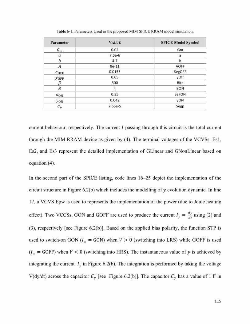
115
Table 6-1. Parameters Used in the proposed MIM SPICE RRAM model simulation.
Parameter VALUE SPICE Model Symbol
𝐺4 0.02 Gm 𝑎 7.5e-6 a 𝑏 4.7 b 𝐴 8e-11 AOFF
𝜎GKK 0.0155 SegOFF 𝑦GKK 0.05 yOff 𝛽 500 Bita 𝐵 4 BON 𝜎GH 0.35 SegON 𝑦GH 0.042 yON 𝜎2 2.65e-5 Segp
current behaviour, respectively. The current 𝐼 passing through this circuit is the total current
through the MIM RRAM device as given by (4). The terminal voltages of the VCVSs: Es1,
Es2, and Es3 represent the detailed implementation of GLinear and GNonLinear based on
equation (4).
In the second part of the SPICE listing, code lines 16–25 depict the implementation of the
circuit structure in Figure 6.2(b) which includes the modelling of𝑦 evolution dynamic. In line
17, a VCVS Epw is used to represents the implementation of the power (due to Joule heating
effect). Two VCCSs, GON and GOFF are used to produce the current 𝐼𝑦 = 𝑑𝑦𝑑𝑡
using (2) and
(3), respectively [see Figure 6.2(b)]. Based on the applied bias polarity, the function STP is
used to switch-on GON (𝐼𝑤 = GON) when 𝑉 > 0 (switching into LRS) while GOFF is used
(𝐼𝑤 = GOFF) when 𝑉 < 0 (switching into HRS). The instantaneous value of 𝑦 is achieved by
integrating the current 𝐼𝑦 in Figure 6.2(b). The integration is performed by taking the voltage
V(dy/dt) across the capacitor 𝐶𝑦 [see Figure 6.2(b)]. The capacitor 𝐶𝑦 has a value of 1 F in
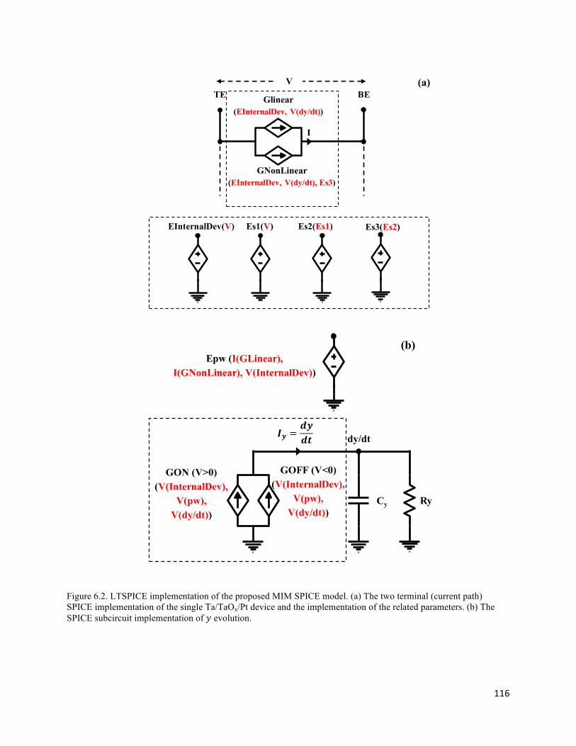
116
Figure 6.2. LTSPICE implementation of the proposed MIM SPICE model. (a) The two terminal (current path) SPICE implementation of the single Ta/TaOx/Pt device and the implementation of the related parameters. (b) The SPICE subcircuit implementation of 𝑦 evolution.
Glinear(EInternalDev, V(dy/dt))
GNonLinear(EInternalDev, V(dy/dt), Es3)
TE BEV
I
Es1(V)EInternalDev(V) Es2(Es1)
(a)
Es3(Es2)
GOFF (V<0)(V(InternalDev),
V(pw),V(dy/dt))
dy/dt
Cy Ry
GON (V>0)(V(InternalDev),
V(pw),V(dy/dt))
𝑰𝒚 =𝒅𝒚𝒅𝒕
(b)Epw (I(GLinear),
I(GNonLinear), V(InternalDev))
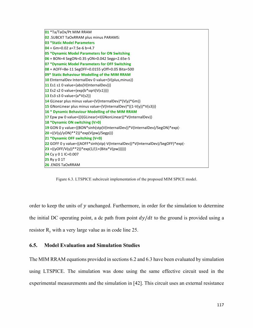
117
01*Ta/TaOx/PtMIMRRAM02.SUBCKTTaOxRRAMplusminusPARAMS:03*StaticModelParameters04+Gm=0.02a=7.5e-6b=4.705*DynamicModelParametersforONSwitching06+BON=4SegON=0.35yON=0.042Segp=2.65e-507*DynamicModelParametersforOFFSwitching08+AOFF=8e-11SegOFF=0.0155yOff=0.05Bita=50009*StaticBehaviourModellingoftheMIMRRAM10EInternalDevInternalDev0value=V(plus,minus)11Es1s10value=abs(V(InternalDev))12Es2s20value=exp(b*sqrt(V(s1)))13Es3s30value=a*V(s2)14GLinearplusminusvalue=V(InternalDev)*(V(y)*Gm)15GNonLinearplusminusvalue=V(InternalDev)*((1-V(y))*V(s3))16*DynamicBehaviourModellingoftheMIMRRAM17Epwpw0value=(I(GLinear)+I(GNonLinear))*V(InternalDev)18*DynamicONswitching(V>0)19GON0yvalue=(BON*sinh(stp(V(InternalDev))*V(InternalDev)/SegON)*exp(-20+((V(y)/yON)**2))*exp(V(pw)/Segp))21*DynamicOFFswitching(V<0)22GOFF0yvalue=(AOFF*sinh(stp(-V(InternalDev))*V(InternalDev)/SegOFF)*exp(-23+((yOFF/V(y))**2))*exp(1/(1+(Bita*V(pw)))))24Cyy01IC=0.00725Ryy01T26.ENDSTaOxRRAM
Figure 6.3. LTSPICE subcircuit implementation of the proposed MIM SPICE model.
order to keep the units of 𝑦 unchanged. Furthermore, in order for the simulation to determine
the initial DC operating point, a dc path from point 𝑑𝑦/𝑑𝑡 to the ground is provided using a
resistor Ry with a very large value as in code line 25.
6.5. Model Evaluation and Simulation Studies
The MIM RRAM equations provided in sections 6.2 and 6.3 have been evaluated by simulation
using LTSPICE. The simulation was done using the same effective circuit used in the
experimental measurements and the simulation in [42]. This circuit uses an external resistance
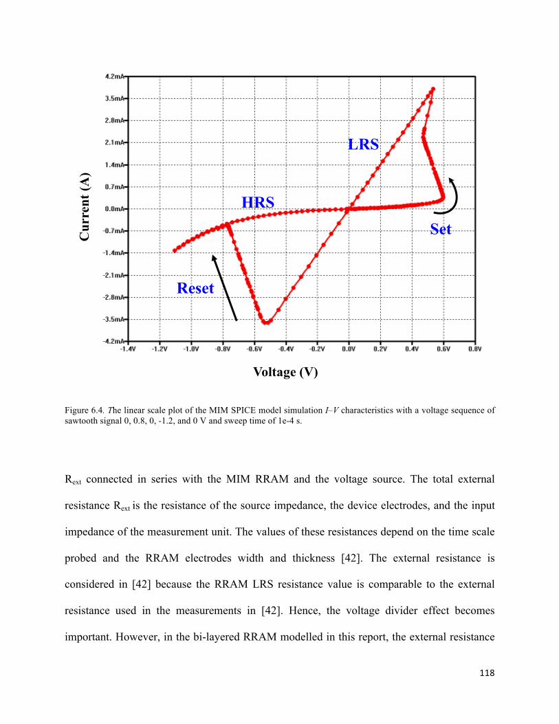
118
Figure 6.4. The linear scale plot of the MIM SPICE model simulation I–V characteristics with a voltage sequence of sawtooth signal 0, 0.8, 0, -1.2, and 0 V and sweep time of 1e-4 s.
Rext connected in series with the MIM RRAM and the voltage source. The total external
resistance Rext is the resistance of the source impedance, the device electrodes, and the input
impedance of the measurement unit. The values of these resistances depend on the time scale
probed and the RRAM electrodes width and thickness [42]. The external resistance is
considered in [42] because the RRAM LRS resistance value is comparable to the external
resistance used in the measurements in [42]. Hence, the voltage divider effect becomes
important. However, in the bi-layered RRAM modelled in this report, the external resistance
Voltage (V)
Set
LRS
HRS
Cur
rent
(A)
Reset
119
of the circuit containing the RRAM device is assumed to be neglected during the experimental
measurement which is why it was not considered in the proposed model in chapters 4 and 5.
Figure 6.4 show the simulation results of the proposed MIM SPICE model obtained using
sawtooth voltage cycle. The voltage sequence of the sawtooth signal is 0, 0.8, 0, -1.2, and 0 V
and the sweep time is 1e-4 s [42]. The value of Rext is 70 Ω. The proposed model is correlated
against several published characteristics of the Ta//TaOx/Pt RRAM and a number of different
insights and matched features emerged. Similar to the simulation results of the analytical MIM
RRAM model obtained in [42], the simulation results in Figure 6.4 show that the device is
switching to LRS and HRS by positive and negative voltage, respectively. Also, the
nonlinearity of the dynamics can be easily observed by abrupt increase and decrease in the
device current as the applied bias reach its positive and negative switching voltages,
respectively, which is in agreement with the characteristic of the MIM RRAM device reported
in [42]. The model also reproduced well most of the I–V characteristics reported in the
experiments in [42]. However, this model is still under developments and more physics-based
insights will be added to the model in the future in order to increase its accuracy and the
reproducibility of the experimental results of the Ta/TaOx/Pt MIM RRAM devices.
120
7. Conclusion and Future Work
CONCLUSION AND FUTURE WORK
In this research, a physics-based mathematical and SPICE models for the Ta2O5/TaOx bi-
layered RRAM have been developed. A new term TPF which manifests the dependency of the
Ta2O5/TaOx bi-layered RRAM current on the physical characteristics of the insulator layer is
used. The proposed models emphasize the effect of the continuous variation of the interface
traps density and the ideality factor on the current conduction. In addition, the oxygen ion
migration mechanism is predicted by deriving the electric field equation for the active region
in the MISM structure. Moreover, the self-limiting growth of the doped region has also been
demonstrated.
The proposed SPICE model offers different adjustable parameters which make it easy to fit the
model into different Ta2O5/TaOx bi-layered RRAM devices with switching layer thickness
smaller than 5 nm (3 and 4 nm). The SPICE model has successfully reproduced all the main
aspects from experimental results for the SET and RESET processes and also the asymmetric
and the symmetric current profiles in HRS and LRS, respectively. The SPICE model can also
demonstrate the current change with regards to RESET pulse signal of different amplitudes.
The developed SPICE model has showed a stable behaviour for its HRS and LRS regions under
three different types of the conventional voltage input signals. Finally, an application of the
121
proposed Ta2O5/TaOx bi-layered RRAM SPICE model as a non-volatile element in the RRAM-
based NV D-latch is demonstrated successfully.
Future work would include more effort on enhancing the proposed models behaviour in HRS
region by taking OCF region into account when designing the model. In addition, future work
involves investigating the possibility to extend the model to represent Ta2O5/TaOx bi-layered
RRAM devices with thicker switching layers and also other bi-layered RRAM physical devices
based on different oxide material. This can be done by verifying the structural models of bi-
layered RRAM devices of different materials using device simulator (e.g. Synopys TCAD). It
also includes studying the temperature dependence, the statistical variability, and the noise
characteristics of the Ta2O5/TaOx bi-layered RRAM devices.
The future work also considers testing the models for the presence of sufficient nonlinearity of
the switching kinetics (second criteria in [44]) and integrating the model in a multi-element
simulation (e.g. two element circuit in a complementary resistive switch) which is the third
criteria in [44]. This is considered as a further verification of the validity of the proposed
models when integrated in a RRAM-based circuit application.
Future work would also include developing a Velilog-A model of the Ta2O5/TaOx bi-layered
RRAM which can also be used in SPICE-based circuit simulations.
122
8. References
References
[1] M.-J. Lee et al., “A fast, high-endurance and scalable non-volatile memory device made from
asymmetric Ta2O5−x/TaO2−x bilayer structures,” Nat. Mater., vol. 10, no. 8, pp. 625–630, 2011.
[2] K. Eshraghian et al., “Memristive device fundamentals and modeling: Applications to circuits and
systems simulation,” in Proceedings of the IEEE, 2012, vol. 100, no. 6, pp. 1991–2007.
[3] H. Liu, D. Bedau, D. Backes, J. A. Katine, J. Langer, and A. D. Kent, “Ultrafast switching in
magnetic tunnel junction based orthogonal spin transfer devices,” Appl. Phys. Lett., vol. 97, no. 24,
pp. 1–3, 2010.
[4] H. F. Hamann, M. O’Boyle, Y. C. Martin, M. Rooks, and H. K. Wickramasinghe, “Ultra-high-
density phase-change storage and memory.,” Nat. Mater., vol. 5, no. May, pp. 383–387, 2006.
[5] N. Setter et al., “Ferroelectric thin films: Review of materials, properties, and applications,” J. Appl.
Phys., vol. 100, no. 5, 2006.
[6] K. Kim and G. Koh, “The prospect on semiconductor memory in nano era,” Proceedings. 7th Int.
Conf. Solid-State Integr. Circuits Technol. 2004., vol. 1, pp. 662–667, 2004.
[7] M. D. Pickett et al., “Switching dynamics in titanium dioxide memristive devices,” J. Appl. Phys.,
vol. 106, no. 7, 2009.
[8] K. M. Kim, S. R. Lee, S. Kim, M. Chang, and C. S. Hwang, “Self-Limited switching in Ta2 O5
/TaOx memristors exhibiting uniform multilevel changes in resistance,” Adv. Funct. Mater., vol. 25,
no. 10, pp. 1527–1534, 2015.
[9] D. B. Strukov, G. S. Snider, D. R. Stewart, and R. S. Williams, “The missing memristor found.,”
Nature, vol. 453, no. 7191, pp. 80–3, 2008.
[10] X. Tang, G. Kim, P.-E. Gaillardon, and G. De Micheli, “A Study on the Programming Structures for
RRAM-Based FPGA Architectures,” IEEE Trans. Circuits Syst. I Regul. Pap., vol. 63, no. 4, pp.
503–516, Apr. 2016.
[11] Y. Xie et al., “A Logic Resistive Memory Chip for Embedded Key Storage With Physical Security,”
IEEE Trans. Circuits Syst. II Express Briefs, vol. 63, no. 4, pp. 336–340, Apr. 2016.
123
[12] P. Stoliar et al., “Nonvolatile Multilevel Resistive Switching Memory Cell: A Transition Metal
Oxide-Based Circuit,” IEEE Trans. Circuits Syst. II Express Briefs, vol. 61, no. 1, pp. 21–25, Jan.
2014.
[13] Y. Zhang, Y. Shen, X. Wang, and L. Cao, “A Novel Design for Memristor-Based Logic Switch and
Crossbar Circuits,” IEEE Trans. Circuits Syst. I Regul. Pap., vol. 62, no. 5, pp. 1402–1411, May
2015.
[14] L. Chua, “Resistance switching memories are memristors,” Appl. Phys. A, vol. 102, no. 4, pp. 765–
783, Mar. 2011.
[15] S. Kvatinsky et al., “TEAM : ThrEshold Adaptive Memristor Model,” Circuits Syst. I Regul. Pap.
IEEE Trans., vol. 60, no. 1, pp. 211–221, 2013.
[16] J. H. Hur, M. J. Lee, C. B. Lee, Y. B. Kim, and C. J. Kim, “Modeling for bipolar resistive memory
switching in transition-metal oxides,” Phys. Rev. B - Condens. Matter Mater. Phys., vol. 82, no. 15,
pp. 1–5, 2010.
[17] J.-H. Hur et al., “Modeling for multilevel switching in oxide-based bipolar resistive memory.,”
Nanotechnology, vol. 23, no. 22, p. 225702, 2012.
[18] S. Kim et al., “Physical electro-thermal model of resistive switching in bi-layered resistance-change
memory.,” Sci. Rep., vol. 3, p. 1680, 2013.
[19] Y. Zhang, N. Deng, H. Wu, Z. Yu, J. Zhang, and H. Qian, “Metallic to hopping conduction transition
in Ta2O5−x/TaOy resistive switching device,” Appl. Phys. Lett., vol. 105, no. 2014, p. 63508, 2014.
[20] J. H. Hur, S. Ryul Lee, M. J. Lee, S. H. Cho, and Y. Park, “Theoretical studies on distribution of
resistances in multilevel bipolar oxide resistive memory by Monte Carlo method,” Appl. Phys. Lett.,
vol. 103, no. 11, pp. 2011–2015, 2013.
[21] F. O. Hatem, P. W. C. Ho, T. N. Kumar, and H. A. F. Almurib, “Modeling of bipolar resistive
switching of a nonlinear MISM memristor,” Semicond. Sci. Technol., vol. 30, no. 11, 2015.
[22] Y. Zhang et al., “Study of conduction and switching mechanisms in Al/AlOx/WOx/W resistive
switching memory for multilevel applications,” Appl. Phys. Lett., vol. 102, no. 23, pp. 1–5, 2013.
[23] F. Yang, M. Wei, and H. Deng, “Bipolar resistive switching characteristics in CuO/ZnO bilayer
structure,” J. Appl. Phys., vol. 114, no. 13, 2013.
[24] S. Yu, Y. Wu, and H. S. P. Wong, “Investigating the switching dynamics and multilevel capability
of bipolar metal oxide resistive switching memory,” Appl. Phys. Lett., vol. 98, no. 10, pp. 2009–
2012, 2011.
[25] P. Huang et al., “A Physics-Based Compact Model of Metal-Oxide-Based RRAM DC and AC
Operations,” IEEE Trans. Electron Devices, vol. 60, no. 12, pp. 4090–4097, Dec. 2013.
[26] M. H. Chiang, K. H. Hsu, W. W. Ding, and B. R. Yang, “A Predictive Compact Model of Bipolar
124
RRAM Cells for Circuit Simulations,” IEEE Trans. Electron Devices, pp. 1–8, 2015.
[27] T. H. Park et al., “Thickness effect of ultra-thin Ta2O5 resistance switching layer in 28 nm-diameter
memory cell,” Sci. Rep., vol. 5, p. 15965, Nov. 2015.
[28] T. H. Park et al., “Thickness-dependent electroforming behavior of ultra-thin Ta2O5 resistance
switching layer,” Phys. status solidi - Rapid Res. Lett., vol. 9, no. 6, pp. 362–365, Jun. 2015.
[29] S. B. Lee et al., “Forming mechanism of the bipolar resistance switching in double-layer memristive
nanodevices,” Nanotechnology, vol. 23, no. 31, p. 315202, 2012.
[30] J. J. Yang et al., “High switching endurance in TaOx memristive devices,” Appl. Phys. Lett., vol. 97,
no. 23, 2010.
[31] A. C. Torrezan, J. P. Strachan, G. Medeiros-Ribeiro, and R. S. Williams, “Sub-nanosecond switching
of a tantalum oxide memristor,” Nanotechnology, vol. 22, no. 48, p. 485203, 2011.
[32] S. M. Sze and K. K. Ng, Physics of Semiconductor Devices: Third Edition. 2006.
[33] H. C. Card et al., “Studies of tunnel MOS diodes I. Interface effects in silicon Schottky diodes,” J.
Phys. D. Appl. Phys., vol. 4, no. 10, p. 319, Oct. 1971.
[34] M. Kazemi, G. E. Rowlands, E. Ipek, R. A. Buhrman, and E. G. Friedman, “Compact Model for
Spin–Orbit Magnetic Tunnel Junctions,” IEEE Trans. Electron Devices, vol. 63, no. 2, pp. 848–855,
Feb. 2016.
[35] G. D. Panagopoulos, C. Augustine, and K. Roy, “Physics-Based SPICE-Compatible Compact Model
for Simulating Hybrid MTJ/CMOS Circuits,” IEEE Trans. Electron Devices, vol. 60, no. 9, pp.
2808–2814, Sep. 2013.
[36] M. Kazemi, E. Ipek, and E. G. Friedman, “Adaptive Compact Magnetic Tunnel Junction Model,”
IEEE Trans. Electron Devices, vol. 61, no. 11, pp. 3883–3891, Nov. 2014.
[37] F. O. Hatem, T. N. Kumar, and H. A. F. Almurib, “A SPICE Model of the Ta2O5/TaOx Bi-Layered
RRAM,” IEEE Trans. Circuits Syst. I Regul. Pap., vol. 63, no. 9, pp. 1487–1498, Sept. 2016.
[38] L. O. Chua, “Memristor—The Missing Circuit Element,” IEEE Trans. Circuit Theory, vol. 18, no.
5, pp. 507–519, 1971.
[39] J. Joshua Yang et al., “The mechanism of electroforming of metal oxide memristive switches.,”
Nanotechnology, vol. 20, no. 21, p. 215201, 2009.
[40] C. Yakopcic, “Generalized Memristive Device SPICE Model and its Application in Circuit Design,”
IEEE Trans. Comput. Des. Integr. Circuits Syst., vol. 32, no. 8, pp. 1201–1214, 2013.
[41] A. Siemon, S. Menzel, A. Marchewka, Y. Nishi, R. Waser, and E. Linn, “Simulation of TaOx-based
complementary resistive switches by a physics-based memristive model,” Proc. - IEEE Int. Symp.
Circuits Syst., no. Iwe Ii, pp. 1420–1423, 2014.
[42] J. P. Strachan et al., “State dynamics and modeling of tantalum oxide memristors,” Electron Devices,
125
IEEE Trans., vol. 60, no. 7, pp. 2194–2202, 2013.
[43] S. Larentis, F. Nardi, S. Balatti, D. C. Gilmer, and D. Ielmini, “Resistive switching by voltage-driven
ion migration in bipolar RRAMPart II: Modeling,” IEEE Trans. Electron Devices, vol. 59, no. 9, pp.
2468–2475, 2012.
[44] E. Linn, A. Siemon, R. Waser, and S. Menzel, “Applicability of well-established memristive models
for simulations of resistive switching devices,” IEEE Trans. Circuits Syst. I Regul. Pap., vol. 61, no.
8, pp. 2402–2410, 2014.
[45] A. S. Oblea, A. Timilsina, D. Moore, and K. A. Campbell, “Silver chalcogenide based memristor
devices,” in The 2010 International Joint Conference on Neural Networks (IJCNN), 2010, pp. 1–3.
[46] F. Miao et al., “Anatomy of a Nanoscale Conduction Channel Reveals the Mechanism of a High-
Performance Memristor,” Adv. Mater., vol. 23, no. 47, pp. 5633–5640, Dec. 2011.
[47] K. Miller, K. S. Nalwa, A. Bergerud, N. M. Neihart, and S. Chaudhary, “Memristive Behavior in
Thin Anodic Titania,” IEEE Electron Device Lett., vol. 31, no. 7, pp. 737–739, Jul. 2010.
[48] K. Miller, “Fabrication and modeling of thin-film anodic titania memristors,” Grad. Theses Diss.,
2010.
[49] S. H. Jo and W. Lu, “CMOS compatible nanoscale nonvolatile resistance switching memory.,” Nano
Lett., vol. 8, no. 2, pp. 392–7, Feb. 2008.
[50] Y. Nishi, S. Schmelzer, U. Bottger, and R. Waser, “Weibull analysis of the kinetics of resistive
switches based on tantalum oxide thin films,” in 2013 Proceedings of the European Solid-State
Device Research Conference (ESSDERC), 2013, pp. 174–177.
[51] H. Li, P. Huang, B. Gao, B. Chen, X. Liu, and J. Kang, “A SPICE model of resistive random access
memory for large-scale memory array simulation,” IEEE Electron Device Lett., vol. 35, no. 2, pp.
211–213, 2014.
[52] N. Jinwoo et al., “Development of a Semiempirical Compact Model for DC/AC Cell Operation of
<formula formulatype=‘inline’> <img src=‘/images/tex/21093.gif’ alt=‘\rm HfO_\rmx’>
</formula>-Based ReRAMs,” Electron Device Lett. IEEE, vol. 34, no. 9, pp. 1133–1135, 2013.
[53] X. Guan, S. Yu, and H.-S. P. Wong, “A SPICE Compact Model of Metal Oxide Resistive
Switching Memory With Variations,” IEEE Electron Device Lett., vol. 33, no. 10, pp. 1405–1407,
2012.
[54] S. Lv, H. Wang, J. Zhang, J. Liu, L. Sun, and S. Member, “An Analytical Model for the Forming
Process of Random-Access Memory,” IEEE Trans. Electron Devices, vol. 61, no. 9, pp. 3166–3171,
2014.
[55] R. Ramprasad, “First principles study of oxygen vacancy defects in tantalum pentoxide,” J. Appl.
Phys., vol. 94, no. 9, pp. 5609–5612, 2003.
126
[56] N. Cabrera and N. F. Mott, “Theory of the oxidation of metals,” Reports Prog. Phys., vol. 12, no. 1,
pp. 163–184, 2002.
[57] D. B. Strukov and R. S. Williams, “Exponential ionic drift: Fast switching and low volatility of thin-
film memristors,” Appl. Phys. A Mater. Sci. Process., vol. 94, no. 3, pp. 515–519, 2009.
[58] S. Yu and H. S. P. Wong, “Compact modeling of conducting-bridge random-access memory
(CBRAM),” IEEE Trans. Electron Devices, vol. 58, no. 5, pp. 1352–1360, 2011.
[59] P. R. Mickel et al., “A physical model of switching dynamics in tantalum oxide memristive devices,”
Appl. Phys. Lett., vol. 102, no. 22, 2013.
[60] S. M. Sze and M. K. Lee, Semiconductor devices, physics and technology. Wiley, 2012.
[61] H. C. Card and E. H. Rhoderick, “Studies of tunnel MOS diodes I. Interface effects in silicon
Schottky diodes,” J. Phys. D. Appl. Phys., vol. 4, no. 10, pp. 1589–1601, 2002.
[62] E. H. ,R. H. W. Rhoderick, “Metal-semiconductor contacts,” Phys. Technol., vol. 5, no. 4, pp. 223–
223, 1988.
[63] J. Bardeen, “Surface states and rectification at a metal semi-conductor contact,” Phys. Rev., vol. 71,
no. 10, pp. 717–727, 1947.
[64] Z. Chen, B. B. Jie, and C.-T. Sah, “Effects of energy distribution of interface traps on recombination
dc current-voltage line shape,” J. Appl. Phys., vol. 100, no. 11, p. 114511, 2006.
[65] J. G. Hwu, C. M. Lin, and W. S. Wang, “Effect of interface traps related to mobile charges on silicon
n-channel metal/oxide/semiconductor field effect transistors determined by a charge-temperature
technique,” Thin Solid Films, vol. 142, no. 2, pp. 183–191, 1986.
[66] U. Russo, D. Ielmini, C. Cagli, and A. L. Lacaita, “Self-accelerated thermal dissolution model for
reset programming in unipolar resistive-switching memory (RRAM) devices,” IEEE Trans. Electron
Devices, vol. 56, no. 2, pp. 193–200, 2009.
[67] N. Mott, Electronic processes in ionic crystals. New York NY: Dover, 1964.
[68] Z. Wei et al., “Highly reliable TaOx ReRAM and direct evidence of redox reaction mechanism,”
2008 IEEE Int. Electron Devices Meet., pp. 1–4, 2008.
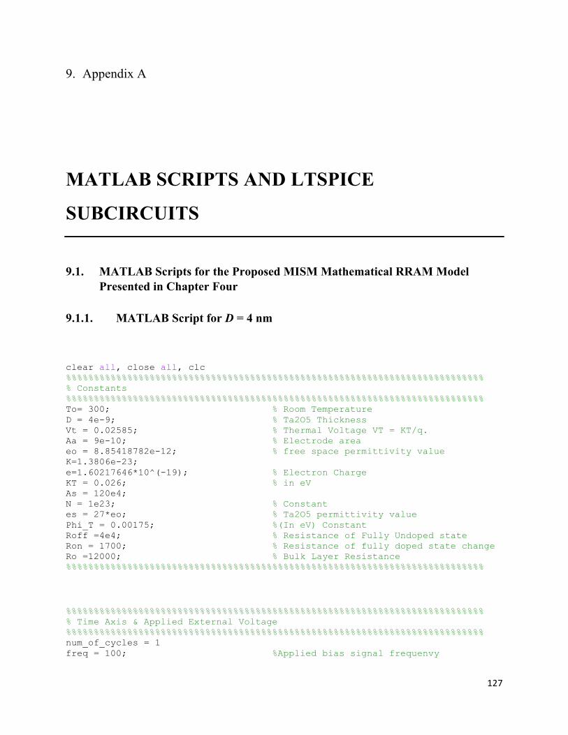
127
9. Appendix A
MATLAB SCRIPTS AND LTSPICE
SUBCIRCUITS
9.1. MATLAB Scripts for the Proposed MISM Mathematical RRAM Model Presented in Chapter Four
9.1.1. MATLAB Script for D = 4 nm
clear all, close all, clc %%%%%%%%%%%%%%%%%%%%%%%%%%%%%%%%%%%%%%%%%%%%%%%%%%%%%%%%%%%%%%%%%%%%%%%%%%% % Constants %%%%%%%%%%%%%%%%%%%%%%%%%%%%%%%%%%%%%%%%%%%%%%%%%%%%%%%%%%%%%%%%%%%%%%%%%%% To= 300; % Room Temperature D = 4e-9; % Ta2O5 Thickness Vt = 0.02585; % Thermal Voltage VT = KT/q. Aa = 9e-10; % Electrode area eo = 8.85418782e-12; % free space permittivity value K=1.3806e-23; e=1.60217646*10^(-19); % Electron Charge KT = 0.026; % in eV As = 120e4; N = 1e23; % Constant es = 27*eo; % Ta2O5 permittivity value Phi_T = 0.00175; %(In eV) Constant Roff =4e4; % Resistance of Fully Undoped state Ron = 1700; % Resistance of fully doped state change Ro =12000; % Bulk Layer Resistance %%%%%%%%%%%%%%%%%%%%%%%%%%%%%%%%%%%%%%%%%%%%%%%%%%%%%%%%%%%%%%%%%%%%%%%%%%% %%%%%%%%%%%%%%%%%%%%%%%%%%%%%%%%%%%%%%%%%%%%%%%%%%%%%%%%%%%%%%%%%%%%%%%%%%% % Time Axis & Applied External Voltage %%%%%%%%%%%%%%%%%%%%%%%%%%%%%%%%%%%%%%%%%%%%%%%%%%%%%%%%%%%%%%%%%%%%%%%%%%% num_of_cycles = 1 freq = 100; %Applied bias signal frequenvy
128
tspan=[0 num_of_cycles/freq]; points=2e4; tspan_vector = linspace(tspan(1),tspan(2),points); amp =2; % Applied bias voltage amplitude V=zeros(size((tspan_vector))); V = amp*sin(freq*2*pi*tspan_vector); %The applied external voltage %%%%%%%%%%%%%%%%%%%%%%%%%%%%%%%%%%%%%%%%%%%%%%%%%%%%%%%%%%%%%%%%%%%%%%%%%%% %%%%%%%%%%%%%%%%%%%%%%%%%%%%%%%%%%%%%%%%%%%%%%%%%%%%%%%%%%%%%%%%%%%%%%%%%%% %RRAM Initial Values - Initial State %%%%%%%%%%%%%%%%%%%%%%%%%%%%%%%%%%%%%%%%%%%%%%%%%%%%%%%%%%%%%%%%%%%%%%%%%%% W=zeros(size((tspan_vector))); W_dot=zeros(size((tspan_vector))); D_Phi=zeros(size((tspan_vector))); Phi_s=zeros(size((tspan_vector))); Eta=zeros(size((tspan_vector))); Phi_B = zeros(size((tspan_vector))); Phi_Bo = zeros(size((tspan_vector))); Is= zeros(size((tspan_vector))); E= zeros(size((tspan_vector))); Vsch=zeros(size((tspan_vector))); VD=zeros(size((tspan_vector))); T=zeros(size((tspan_vector))); R=zeros(size((tspan_vector))); % The initial state of the RRAM is the fully doped state w=0 (LRS) w_init = 0.0; W0=w_init*D; delta_t=tspan_vector(2)-tspan_vector(1); W(1)=W0; R(1) = Ron+Ro; Itun(1) = V(1)/R(1); T(1)=300; Vsch(1)=(V(1)-(Itun(1).*R(1))); %%%%%%%%%%%%%%%%%%%%%%%%%%%%%%%%%%%%%%%%%%%%%%%%%%%%%%%%%%%%%%%%%%%%%%%%%%% %%%%%%%%%%%%%%%%%%%%%%%%%%%%%%%%%%%%%%%%%%%%%%%%%%%%%%%%%%%%%%%%%%%%%%%%%%% %Schottky Barrier and tunneling equations %%%%%%%%%%%%%%%%%%%%%%%%%%%%%%%%%%%%%%%%%%%%%%%%%%%%%%%%%%%%%%%%%%%%%%%%%%% f=1e13; a=1e-9; U=1; Rth=1e8; for i=2:length(tspan_vector) Phi_Bo(i-1)=0.6.*((W(i-1)./D)); D_Phi(i-1) = ((((e^3).*N.*Phi_Bo(i-1))/((8.*(pi^2)).*es^3))^.25); Phi_B(i-1) = Phi_Bo(i-1) - D_Phi(i-1); R(i-1)=(Ro+(Ron*(D-W(i-1))/D)+(Roff*W(i-1)/D)); Eta(i-1)=60000*((1000*(D-W(i-1))/D)+(900*W(i-1)/D)); if V(i-1) < 0
129
Is(i-1)=Aa*As*(To^2)*exp(-Phi_B(i-1)./(5.35*K*To/e)); Itun(i)=Is(i-1).*(exp(Vsch(i-1)./(Eta(i-1).*Vt))-1).*exp(-W(i-1)*1e10*sqrt(Phi_T)); elseif V(i-1) >= 0 Is(i-1)=Aa*As*(To^2)*exp(-Phi_B(i-1)./(85*K*To/e)); Itun(i)=-Is(i-1).*(exp(-Vsch(i-1)./(Eta(i-1).*Vt))-1).*exp(-W(i-1)*1e10*sqrt(Phi_T)); end; if V(i) <= 0 Vsch(i)=(V(i)-(Itun(i).*R(i-1))); VD(i)=(V(i)-(Itun(i).*Ro)-Vsch(i)); E(i)=VD(i)./(W(i-1)+((Ron/Roff)*(D-W(i-1)))); T(i)=To+(Rth*(Itun(i)^2*(R(i-1)-Ro))); W_dot(i)=a*f.*exp(-U*e/(K*T(i))).*sinh((163*e*a*E(i))/(1*K*T(i))); elseif V(i)>0 V(i) = 3*sin(freq*2*pi*tspan_vector(i)); Vsch(i)=(V(i)-(Itun(i).*R(i-1))); VD(i)=(V(i)-(Itun(i).*Ro)-Vsch(i)); E(i)=VD(i)./(W(i-1)+((Ron/Roff)*(D-W(i-1)))); T(i)=To+(Rth*(Itun(i)^2*(R(i-1)-Ro))); W_dot(i)=.6e-6*a*f.*exp(-U*e/(K*T(i))).*sinh((.4*e*a*E(i))/(1*K*T(i))); end; W(i)=W(i-1)+W_dot(i)*delta_t; if W(i) <= 0 W(i) = 0; W_dot(i)=0; elseif W(i) > D W(i) = D; W_dot(i)=D; end end %%%%%%%%%%%%%%%%%%%%%%%%%%%%%%%%%%%%%%%%%%%%%%%%%%%%%%%%%%%%%%%%%%%%%%%%%%% %Simulation Plots %%%%%%%%%%%%%%%%%%%%%%%%%%%%%%%%%%%%%%%%%%%%%%%%%%%%%%%%%%%%%%%%%%%%%%%%%%% subplot(2,4,1) plot(tspan_vector,W/D,'r'); subplot(2,4,2) plot(tspan_vector,V); title('V-t curve'); xlabel('T[Sec]'); ylabel('V[Volts]'); subplot(2,4,3) plot(W/D,E); title('V-E curve'); xlabel('W/D'); ylabel('E (V/m)');
130
subplot(2,4,4) plot(tspan_vector,Itun); title('I-t curve'); xlabel('T[Sec]'); ylabel('I[Amps]'); subplot(2,4,5) plot(V,Itun); title('It-V1 Linear curve'); xlabel('V1[volt]'); ylabel('It[amp]'); subplot(2,4,6) plot(tspan_vector,Vsch) title('Vsch'); xlabel('T[Sec]'); ylabel('Vsch[volt]'); subplot(2,4,7) plot(V,R); % title(''); xlabel('Voltage(V)'); ylabel('Resistance(?)'); subplot(2,4,8) plot(V, Phi_B); xlabel('Voltage(V)'); ylabel('Phi_b[eV]'); %Matlab model Results - I-V data=xlsread('D4nm_ExpData.xlsx'); xAxis=data(:,1); yAxis=data(:,2); figure(2); semilogy(V,abs(Itun)); hold; semilogy(xAxis,abs(yAxis)); xlabel('Voltage (V)'); ylabel('Current (V)'); % SPICE model Results - Semilog I-V data1=xlsread('SPICE_D4nm.xlsx'); xAxis1=data1(:,1); yAxis1=data1(:,2); xAxis2=data1(:,3); yAxis2=data1(:,4); figure(3); semilogy(xAxis1,abs(yAxis1)); hold; semilogy(xAxis2,abs(yAxis2)); % plot(xAxis1,yAxis1,xAxis2,yAxis2); xlabel('Bias Voltage (V)'); ylabel('Current (A)'); %SPICE model Results - Linear I-V data1=xlsread('SPICE_D4nm_ForLinearIV.xlsx');
131
xAxis1=data1(:,1); yAxis1=data1(:,2); xAxis2=data1(:,3); yAxis2=data1(:,4); figure(4); plot(xAxis1,(yAxis1)); hold; plot(xAxis2,(yAxis2)); xlabel('Bias Voltage (V)'); ylabel('Current (A)'); figure(5); semilogy(V,abs(E)); xlabel('Voltage (V)'); ylabel('E (V/m)'); figure(6); plot(tspan_vector,VD,'g'); hold; plot(tspan_vector,Itun*Ro,'b',tspan_vector,Vsch,'r'); title('VD-Itun*Ro-Vsch'); xlabel('T[Sec]'); ylabel('V[volt]'); figure(7); plotyy(tspan_vector,VD,tspan_vector,R-Ro,'plot','plot'); xlabel('T[Sec]'); ylabel('Ri'); %SPICE model Results - The temporal increase in HRS data2=xlsread('Temp_Incr_HRS.xlsx'); yAxis01=data2(:,1); yAxis02=data2(:,2); yAxis03=data2(:,3); yAxis04=data2(:,4); yAxis05=data2(:,5); yAxis06=data2(:,6); yAxis07=data2(:,7); yAxis08=data2(:,8); figure(8); plot(yAxis01,yAxis02,'g'); hold; plot(yAxis01,yAxis03,'b',yAxis01,yAxis04,yAxis01,yAxis05); figure(9); plotyy(yAxis01,yAxis07,yAxis01,yAxis08,'plot','plot'); %SPICE model Results - Triangular data3=xlsread('Tria_Input.xlsx'); yAxis001=data3(:,1); yAxis002=data3(:,2); yAxis003=data3(:,3); figure(10); plotyy(yAxis001,yAxis003,yAxis001,yAxis002,'plot','plot'); %SPICE model Results - Rectangular
132
data4=xlsread('Rect_Input.xlsx'); yAxis0001=data4(:,1); yAxis0002=data4(:,2); yAxis0003=data4(:,3); figure(11); plotyy(yAxis0001,yAxis0003,yAxis0001,yAxis0002,'plot','plot'); %SPICE model Results - SinglePulseReset_SAMSUNG data5=xlsread('Single_RESET_Pulse.xlsx'); yAxis0000001=data5(:,1); yAxis0000002=data5(:,2); yAxis0000003=data5(:,3); yAxis0000004=data5(:,4); yAxis0000005=data5(:,5); yAxis0000006=data5(:,6); yAxis0000007=data5(:,7); figure(12); plotyy(yAxis0000001,yAxis0000003,yAxis0000001,yAxis0000002,'plot','plot'); hold plot(yAxis0000005,yAxis0000007); figure(13); plotyy(yAxis0000001,yAxis0000004,yAxis0000001,yAxis0000002,'plot','plot'); hold plot(yAxis0000005,yAxis0000006);
9.1.2. MATLAB Script for D = 3 nm.
clear all, close all, clc %%%%%%%%%%%%%%%%%%%%%%%%%%%%%%%%%%%%%%%%%%%%%%%%%%%%%%%%%%%%%%%%%%%%%%%%%%% % Constants %%%%%%%%%%%%%%%%%%%%%%%%%%%%%%%%%%%%%%%%%%%%%%%%%%%%%%%%%%%%%%%%%%%%%%%%%%% To= 300; % Room Temperature D = 3e-9; % Ta2O5 Thickness Vt = 0.02585; % Thermal Voltage VT = KT/q. Aa = 9e-10; % Electrode area eo = 8.85418782e-12; % free space permittivity value K=1.3806e-23; e=1.60217646*10^(-19); % Electron Charge KT = 0.026; % in eV As = 120e4; N = 1e23; % Constant es = 27*eo; % Ta2O5 permittivity value Phi_T = 0.0031; %(Phi_T In eV) Constant Roff =2e4; Ron = 1700; Ro =12000; %%%%%%%%%%%%%%%%%%%%%%%%%%%%%%%%%%%%%%%%%%%%%%%%%%%%%%%%%%%%%%%%%%%%%%%%%%% %%%%%%%%%%%%%%%%%%%%%%%%%%%%%%%%%%%%%%%%%%%%%%%%%%%%%%%%%%%%%%%%%%%%%%%%%%% % Time Axis & Applied External Voltage
133
%%%%%%%%%%%%%%%%%%%%%%%%%%%%%%%%%%%%%%%%%%%%%%%%%%%%%%%%%%%%%%%%%%%%%%%%%%% num_of_cycles = 1 freq = .2; %Applied bias signal frequenvy tspan=[0 num_of_cycles/freq]; points=2e4; %Increase this for high indurance results tspan_vector = linspace(tspan(1),tspan(2),points); amp =2; % Applied bias voltage amplitude V=zeros(size((tspan_vector))); V = amp*sin(freq*2*pi*tspan_vector); %The applied external voltage %%%%%%%%%%%%%%%%%%%%%%%%%%%%%%%%%%%%%%%%%%%%%%%%%%%%%%%%%%%%%%%%%%%%%%%%%%% %%%%%%%%%%%%%%%%%%%%%%%%%%%%%%%%%%%%%%%%%%%%%%%%%%%%%%%%%%%%%%%%%%%%%%%%%%% %RRAM Initial Values - Initial State %%%%%%%%%%%%%%%%%%%%%%%%%%%%%%%%%%%%%%%%%%%%%%%%%%%%%%%%%%%%%%%%%%%%%%%%%%% W=zeros(size((tspan_vector))); W_dot=zeros(size((tspan_vector))); D_Phi=zeros(size((tspan_vector))); Phi_s=zeros(size((tspan_vector))); Eta=zeros(size((tspan_vector))); Phi_B = zeros(size((tspan_vector))); Phi_Bo = zeros(size((tspan_vector))); Is= zeros(size((tspan_vector))); E= zeros(size((tspan_vector))); Vsch=zeros(size((tspan_vector))); VD=zeros(size((tspan_vector))); T=zeros(size((tspan_vector))); R=zeros(size((tspan_vector))); % The initial state of the RRAM is the fully doped state w=0 (LRS) w_init = 0.0; W0=w_init*D; delta_t=tspan_vector(2)-tspan_vector(1); W(1)=W0; R(1) = Ron+Ro; Itun(1) = V(1)/R(1); T(1)=300; Vsch(1)=(V(1)-(Itun(1).*R(1))); %%%%%%%%%%%%%%%%%%%%%%%%%%%%%%%%%%%%%%%%%%%%%%%%%%%%%%%%%%%%%%%%%%%%%%%%%%% %%%%%%%%%%%%%%%%%%%%%%%%%%%%%%%%%%%%%%%%%%%%%%%%%%%%%%%%%%%%%%%%%%%%%%%%%%% %Schottky Barrier and tunneling equations %%%%%%%%%%%%%%%%%%%%%%%%%%%%%%%%%%%%%%%%%%%%%%%%%%%%%%%%%%%%%%%%%%%%%%%%%%% f=1e13; a=1e-9; Ea=1; Rth=1e8; for i=2:length(tspan_vector) Phi_Bo(i-1)=0.45.*((W(i-1)./D)); D_Phi(i-1) = ((((e^3).*N.*Phi_Bo(i-1))/((8.*(pi^2)).*es^3))^.25); Phi_B(i-1) = Phi_Bo(i-1) - D_Phi(i-1);
134
R(i-1)=(Ro+(Ron*(D-W(i-1))/D)+(Roff*W(i-1)/D)); Eta(i-1)=60000*((1000*(D-W(i-1))/D)+(900*W(i-1)/D)); if V(i-1) < 0 Is(i-1)=Aa*As*(To^2)*exp(-Phi_B(i-1)./((5.25*K*To/e))); Itun(i)=Is(i-1).*(exp(Vsch(i-1)./(Eta(i-1).*Vt))-1).*exp(-W(i-1)*1e10*sqrt(Phi_T)); elseif V(i-1) >= 0 Is(i-1)=Aa*As*(To^2)*exp(-Phi_B(i-1)./(2000*(K*To/e))); Itun(i)=-Is(i-1).*(exp(-Vsch(i-1)./(Eta(i-1).*Vt))-1).*exp(-W(i-1)*1e10*sqrt(Phi_T)); end; if V(i) <= 0 Vsch(i)=(V(i)-(Itun(i).*R(i-1))); VD(i)=(V(i)-(Itun(i).*Ro)-Vsch(i)); E(i)=VD(i)./(W(i-1)+((Ron/Roff)*(D-W(i-1)))); T(i)=To+(Rth*(Itun(i)^2*(R(i-1)-Ro))); W_dot(i)=a*f.*exp(-Ea*e/(K*T(i))).*sinh((55*e*a*E(i))/(1*K*T(i))); elseif V(i)>0 V(i) = 3*sin(freq*2*pi*tspan_vector(i)); Vsch(i)=(V(i)-(Itun(i).*R(i-1))); VD(i)=(V(i)-(Itun(i).*Ro)-Vsch(i)); E(i)=VD(i)./(W(i-1)+((Ron/Roff)*(D-W(i-1)))); T(i)=To+(Rth*(Itun(i)^2*(R(i-1)-Ro))); W_dot(i)=.6e-6*a*f.*exp(-Ea*e/(K*T(i))).*sinh((0.02*e*a*E(i))/(1*K*T(i))); end; W(i)=W(i-1)+W_dot(i)*delta_t; if W(i) <= 0 W(i) = 0; W_dot(i)=0; elseif W(i) > D W(i) = D; W_dot(i)=D; end end %%%%%%%%%%%%%%%%%%%%%%%%%%%%%%%%%%%%%%%%%%%%%%%%%%%%%%%%%%%%%%%%%%%%%%%%%%% %Simulation Plots %%%%%%%%%%%%%%%%%%%%%%%%%%%%%%%%%%%%%%%%%%%%%%%%%%%%%%%%%%%%%%%%%%%%%%%%%%% subplot(2,4,1) plot(tspan_vector,W/D,'r'); subplot(2,4,2) plot(tspan_vector,V); title('V-t curve'); xlabel('T[Sec]'); ylabel('V[Volts]'); subplot(2,4,3) plot(W/D,E); title('V-E curve'); xlabel('W/D'); ylabel('E (V/m)');
135
subplot(2,4,4) plot(tspan_vector,Itun); title('I-t curve'); xlabel('T[Sec]'); ylabel('I[Amps]'); subplot(2,4,5) plot(V,Itun); xlabel('V1[volt]'); ylabel('It[amp]'); subplot(2,4,6) plot(W/D,Vsch); title('Vsch'); xlabel('T[Sec]'); ylabel('Vsch[volt]'); subplot(2,4,7) plot(V,R); % title(''); xlabel('Voltage(V)'); ylabel('Resistance(?)'); subplot(2,4,8) plot(V, Phi_B); xlabel('Voltage(V)'); ylabel('?_b[eV]'); %Matlab model Results data=xlsread('D3nm_ExpData.xlsx'); xAxis=data(:,1); yAxis=data(:,2); figure(2); semilogy(V,abs(Itun)); hold; semilogy(xAxis,abs(yAxis)); % title('It-V1 semilogy curve'); xlabel('Voltage (V)'); ylabel('Current (V)'); %SPICE model Results data1=xlsread('SPICE_D3nm.xlsx'); xAxis1=data1(:,1); yAxis1=data1(:,2); xAxis2=data1(:,3); yAxis2=data1(:,4); figure(3); semilogy(xAxis1,abs(yAxis1)); hold; semilogy(xAxis2,abs(yAxis2)); xlabel('Bias Voltage (V)'); ylabel('Current (A)'); figure(4); semilogy(V,abs(E)); xlabel('Voltage (V)');
136
ylabel('E (V/m)'); %SPICE model Results-Pulse data2=xlsread('SPICE_D3nm_Pulse.xlsx'); xAxis3=data2(:,1); yAxis3=data2(:,2); xAxis4=data2(:,3); yAxis4=data2(:,4); figure(5); plot(xAxis3,yAxis3); hold; plot(xAxis4,yAxis4); xlabel('Bias Voltage (V)'); ylabel('Current (A)'); % Linear I-V curve (Matlab Result) figure(6); plot(V,Itun); xlabel('V1[volt]'); ylabel('It[amp]'); %SPICE model Results - Different Sweep Rates (SPICE Model Results) % Make amp =3; freq = 0.2, 2, and 20 Hz data3=xlsread('SPICE_D3nm_DifferentSweepRates.xlsx'); xAxis5=data3(:,1); yAxis5=data3(:,2); xAxis6=data3(:,3); yAxis6=data3(:,4); xAxis7=data3(:,5); yAxis7=data3(:,6); figure(7); plot(xAxis5,yAxis5, 'b',xAxis6,yAxis6, 'g'); hold; plot(xAxis7,yAxis7,'r'); xlabel('Bias Voltage (V)'); ylabel('Current (A)');
9.2. SPICE Subcircuit for the Proposed MISM SPICE RRAM Model Presented in Chapter Five
9.2.1. SPICE Subcircuit for D = 4 nm
.SUBCKTTaOxRRAMplusminusTPFPhi_bVsPARAMS:
+T0=300D=4e-9VT=0.02585Ar=9e-10e0=8.85418782e-12
+k=1.3806e-23q=1.60217646e-19As=120e4es=27*e0N=1e23
+Phi_T=0.00175Roff=40kRon=1.7kRo=12kf=1e13a=1e-9U=1Rth=1e8
+x1=215x2=0.4v1=1v2=0.6e-6n1=0.1852n2=0.0117m=6e6
137
EVV0value=V(plus)-V(minus)
EPhi_BnPhi_Bn0value=0.6*V(w)/D
ED_PhiD_Phi0value=(((q**3)*N*V(Phi_Bn))/(8*(pi**2)*(es**3)))**0.25
EPhi_bPhi_b0value=V(Phi_Bn)-V(D_Phi)
EEtaEta0value=m*((10*(D-V(w))/D)+(9*V(w)/D))
ETPFTPF0value=exp(-V(w)*sqrt(Phi_T)*1e10)
ERsRs0value=Ro+(Ron*(D-V(w))/D)+(Roff*V(w)/D)
EVRsPVsminusvalue=V(Rs)*I(EVRs)
EVsVs0value=V(V)-(I(EVRs)*V(Rs))
*ONswitchingCurrect(V<0)
EIsOnIsOn0value=stp(-V(V))*Ar*As*(T0**2)*exp(-n1*V(Phi_b)/(k*T0/q))
GItunONplusPVsvalue=V(IsOn)*(exp(V(Vs)/(V(Eta)*VT))-1)*V(TPF)
*Eaa1aa10value=(exp(V(Vs)/(V(Eta)*Vt))-1)
*OFFswitchingCurrent(V>=0)
EIsOffIsOff0value=stp(V(V))*Ar*As*(T0**2)*exp(-n2*V(Phi_b)/(k*T0/q))
GItunOFFplusPVsvalue=(-V(IsOff))*(exp(-V(Vs)/(V(Eta)*VT))-1)*V(TPF)
************************************************
*DynamicalModel-Differentialequationmodeling*
************************************************
EVDVD0value=V(V)-(I(EVRs)*Ro)-V(Vs)
EEuEu0value=V(VD)/(V(w)+((Ron/Roff)*(D-V(w))))
ETT0value=T0+(Rth*(I(EVRs)**2)*(V(Rs)-Ro))
EKTKT0value=k*V(T)
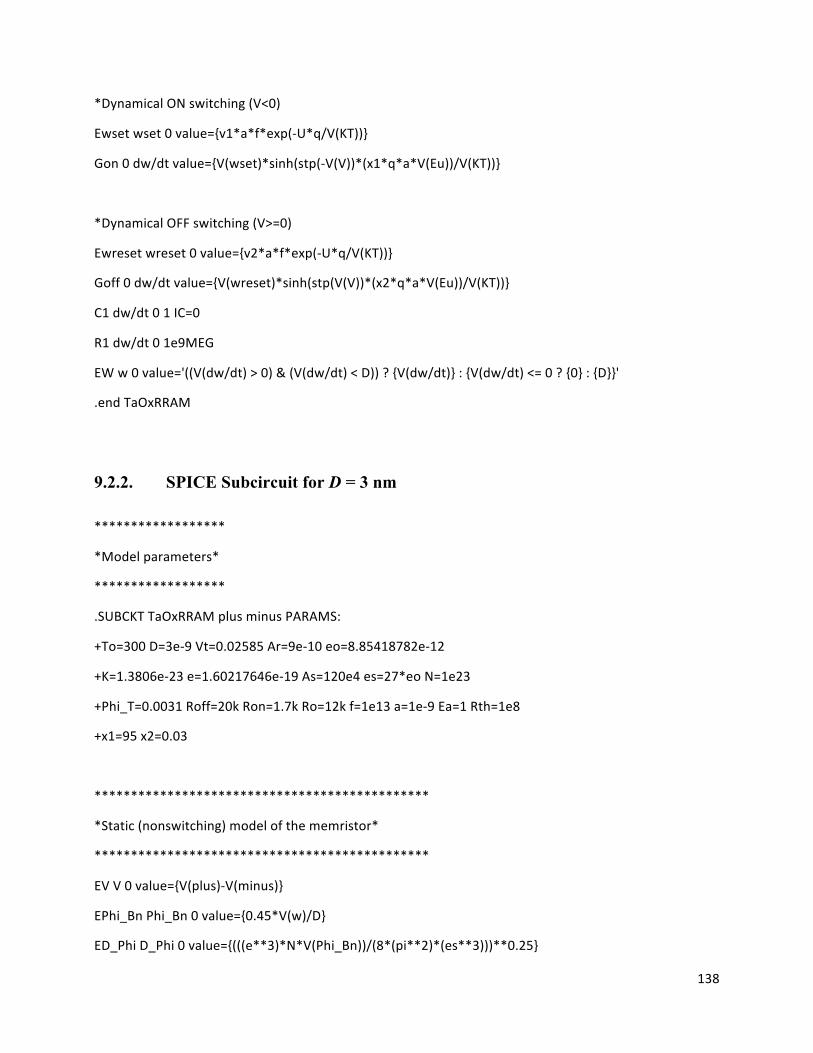
138
*DynamicalONswitching(V<0)
Ewsetwset0value=v1*a*f*exp(-U*q/V(KT))
Gon0dw/dtvalue=V(wset)*sinh(stp(-V(V))*(x1*q*a*V(Eu))/V(KT))
*DynamicalOFFswitching(V>=0)
Ewresetwreset0value=v2*a*f*exp(-U*q/V(KT))
Goff0dw/dtvalue=V(wreset)*sinh(stp(V(V))*(x2*q*a*V(Eu))/V(KT))
C1dw/dt01IC=0
R1dw/dt01e9MEG
EWw0value='((V(dw/dt)>0)&(V(dw/dt)<D))?V(dw/dt):V(dw/dt)<=0?0:D'
.endTaOxRRAM
9.2.2. SPICE Subcircuit for D = 3 nm
******************
*Modelparameters*
******************
.SUBCKTTaOxRRAMplusminusPARAMS:
+To=300D=3e-9Vt=0.02585Ar=9e-10eo=8.85418782e-12
+K=1.3806e-23e=1.60217646e-19As=120e4es=27*eoN=1e23
+Phi_T=0.0031Roff=20kRon=1.7kRo=12kf=1e13a=1e-9Ea=1Rth=1e8
+x1=95x2=0.03
**********************************************
*Static(nonswitching)modelofthememristor*
**********************************************
EVV0value=V(plus)-V(minus)
EPhi_BnPhi_Bn0value=0.45*V(w)/D
ED_PhiD_Phi0value=(((e**3)*N*V(Phi_Bn))/(8*(pi**2)*(es**3)))**0.25
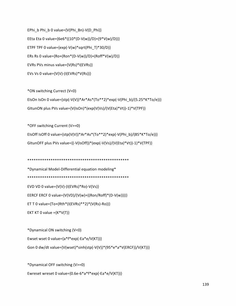
139
EPhi_bPhi_b0value=V(Phi_Bn)-V(D_Phi)
EEtaEta0value=6e6*((10*(D-V(w))/D)+(9*V(w)/D))
ETPFTPF0value=exp(-V(w)*sqrt(Phi_T)*30/D)
ERsRs0value=Ro+(Ron*(D-V(w))/D)+(Roff*V(w)/D)
EVRsPVsminusvalue=V(Rs)*I(EVRs)
EVsVs0value=V(V)-(I(EVRs)*V(Rs))
*ONswitchingCurrect(V<0)
EIsOnIsOn0value=stp(-V(V))*Ar*As*(To**2)*exp(-V(Phi_b)/(5.25*K*To/e))
GItunONplusPVsvalue=V(IsOn)*(exp(V(Vs)/(V(Eta)*Vt))-1)*V(TPF)
*OFFswitchingCurrent(V>=0)
EIsOffIsOff0value=stp(V(V))*Ar*As*(To**2)*exp(-V(Phi_b)/(85*K*To/e))
GItunOFFplusPVsvalue=(-V(IsOff))*(exp(-V(Vs)/(V(Eta)*Vt))-1)*V(TPF)
************************************************
*DynamicalModel-Differentialequationmodeling*
************************************************
EVDVD0value=V(V)-(I(EVRs)*Ro)-V(Vs)
EERCFERCF0value=V(VD)/(V(w)+((Ron/Roff)*(D-V(w))))
ETT0value=To+(Rth*(I(EVRs)**2)*(V(Rs)-Ro))
EKTKT0value=K*V(T)
*DynamicalONswitching(V<0)
Ewsetwset0value=a*f*exp(-Ea*e/V(KT))
Gon0dw/dtvalue=V(wset)*sinh(stp(-V(V))*(95*e*a*V(ERCF))/V(KT))
*DynamicalOFFswitching(V>=0)
Ewresetwreset0value=0.6e-6*a*f*exp(-Ea*e/V(KT))

140
Goff0dw/dtvalue=V(wreset)*sinh(stp(V(V))*(0.03*e*a*V(ERCF))/V(KT))
C1dw/dt01IC=0
R1dw/dt01e9MEG
EWw0value='((V(dw/dt)>0)&(V(dw/dt)<D))?V(dw/dt):V(dw/dt)<=0?0:D'
.endTaOxMemristor


![Resistive switching in Pt/TiO 2/Pt - COnnecting REpositories · 2016. 5. 26. · Resistive switching of transition metal oxide (TMO) materials including TiO2[1 3], NiO[4, 5], and](https://static.fdocuments.in/doc/165x107/60c06d4ba8da2d61d21f28d3/resistive-switching-in-pttio-2pt-connecting-repositories-2016-5-26-resistive.jpg)