Biofunctionalized AlGaN/GaN high electron mobility transistor for DNA hybridization detection
5
Biofunctionalized AlGaN/GaN high electron mobility transistor for DNA hybridization detection Resham Thapa, Siddharth Alur, Kyusang Kim, Fei Tong, Yogesh Sharma et al. Citation: Appl. Phys. Lett. 100, 232109 (2012); doi: 10.1063/1.4727895 View online: http://dx.doi.org/10.1063/1.4727895 View Table of Contents: http://apl.aip.org/resource/1/APPLAB/v100/i23 Published by the American Institute of Physics. Related Articles Silicon-based reproducible and active surface-enhanced Raman scattering substrates for sensitive, specific, and multiplex DNA detection Appl. Phys. Lett. 100, 203104 (2012) Cantilever deflection associated with hybridization of monomolecular DNA film J. Appl. Phys. 111, 074310 (2012) Integrated microfluidic chip for rapid DNA digestion and time-resolved capillary electrophoresis analysis Biomicrofluidics 6, 012818 (2012) Rapid multi sample DNA amplification using rotary-linear polymerase chain reaction device (PCRDisc) Biomicrofluidics 6, 014119 (2012) Artificial DNA nanostructure detection using solution-processed In-Ga-Zn-O thin-film transistors Appl. Phys. Lett. 100, 103702 (2012) Additional information on Appl. Phys. Lett. Journal Homepage: http://apl.aip.org/ Journal Information: http://apl.aip.org/about/about_the_journal Top downloads: http://apl.aip.org/features/most_downloaded Information for Authors: http://apl.aip.org/authors Downloaded 13 Jun 2012 to 131.204.47.119. Redistribution subject to AIP license or copyright; see http://apl.aip.org/about/rights_and_permissions
description
AlGaN/GaN HEMT, HEMT Transistor, DNA, DNA Hybridization, Sensor
Transcript of Biofunctionalized AlGaN/GaN high electron mobility transistor for DNA hybridization detection
Biofunctionalized AlGaN/GaN high electron mobility transistor for DNAhybridization detectionResham Thapa, Siddharth Alur, Kyusang Kim, Fei Tong, Yogesh Sharma et al. Citation: Appl. Phys. Lett. 100, 232109 (2012); doi: 10.1063/1.4727895 View online: http://dx.doi.org/10.1063/1.4727895 View Table of Contents: http://apl.aip.org/resource/1/APPLAB/v100/i23 Published by the American Institute of Physics. Related ArticlesSilicon-based reproducible and active surface-enhanced Raman scattering substrates for sensitive, specific, andmultiplex DNA detection Appl. Phys. Lett. 100, 203104 (2012) Cantilever deflection associated with hybridization of monomolecular DNA film J. Appl. Phys. 111, 074310 (2012) Integrated microfluidic chip for rapid DNA digestion and time-resolved capillary electrophoresis analysis Biomicrofluidics 6, 012818 (2012) Rapid multi sample DNA amplification using rotary-linear polymerase chain reaction device (PCRDisc) Biomicrofluidics 6, 014119 (2012) Artificial DNA nanostructure detection using solution-processed In-Ga-Zn-O thin-film transistors Appl. Phys. Lett. 100, 103702 (2012) Additional information on Appl. Phys. Lett.Journal Homepage: http://apl.aip.org/ Journal Information: http://apl.aip.org/about/about_the_journal Top downloads: http://apl.aip.org/features/most_downloaded Information for Authors: http://apl.aip.org/authors
Downloaded 13 Jun 2012 to 131.204.47.119. Redistribution subject to AIP license or copyright; see http://apl.aip.org/about/rights_and_permissions
Biofunctionalized AlGaN/GaN high electron mobility transistor for DNAhybridization detection
Resham Thapa,1 Siddharth Alur,1 Kyusang Kim,1 Fei Tong,1 Yogesh Sharma,1 Moonil Kim,2
Claude Ahyi,1 Jing Dai,3 Jong Wook Hong,3 Michael Bozack,1 John Williams,1
Ahjeong Son,4 Amir Dabiran,5 and Minseo Park1,a)
1Department of Physics, Auburn University, Auburn, Alabama 36849, USA2Department of Pathobiology, Tuskegee University, Tuskegee, Alabama 36088, USA3Materials Research and Education Center, Auburn University, Auburn, Alabama 36849, USA4Department of Civil Engineering, Auburn University, Auburn, Alabama 36849, USA5SVT Associates, Inc., Eden Prairie, Minnesota 55344, USA
(Received 4 January 2012; accepted 18 May 2012; published online 7 June 2012)
Label-free electrical detection of deoxyribonucleic acid (DNA) hybridization was demonstrated
using an AlGaN/GaN high electron mobility transistor (HEMT) based transducer with a
biofunctionalized gate. The HEMT DNA sensor employed the immobilization of amine-modified
single strand DNA on the self-assembled monolayers of 11-mercaptoundecanoic acid. The sensor
exhibited a substantial current drop upon introduction of complimentary DNA to the gate well,
which is a clear indication of the hybridization. The application of 3 base-pair mismatched target
DNA showed little change in output current characteristics of the transistor. Therefore, it can be
concluded that our DNA sensor is highly specific to DNA sequences. VC 2012 American Institute ofPhysics. [http://dx.doi.org/10.1063/1.4727895]
Current trends for the sensors are toward the simpler,
faster, and miniature devices that do not require costly
reagents, bulky instrumentation setups, operating skills, etc.
At present, deoxyribonucleic acid (DNA) sequencing and
detection are essentially associated with the semi-automated
laboratory settings and are mainly available to the central-
ized locations.1 Considering the commercial demands, cur-
rent capabilities for the DNA sequencing are limited. Most
of the existing methods involve pre-labeling of the molecule
analytes. Associated costs and technology requirements of-
ten make the current commercial detection schemes unsuit-
able for large screening programs.2
With the advancement in the semiconductor material
growth and sophisticated device fabrication technology, fully
electronic biosensors are the potential successors to a wide
range of analytical sensors. In this regard, hybridization
based electrical DNA detection techniques implementing
field-effect transistors (FET) are very convenient for diag-
nostic and comparative sequencing.3–6 Aluminum gallium
nitride/gallium nitride (AlGaN/GaN) heterostructure with
their superior material characteristics such as non-toxicity to
the living cells, higher chemical and thermal stability, higher
sensitivity, higher energy bandgap, etc. presents an attractive
platform for the fabrication of the FET based biosensor.7,8
Fabricating an array of suitably spaced transistors permits
the multi-parameter detection without using markers and
labels as used in conventional DNA detection schemes. In
addition, AlGaN/GaN high electron mobility transistor
(HEMT) based DNA sensor can be operated without the ref-
erence electrode, which greatly reduces volume of the
reagents necessary for the detection and also simplifies the
experimental setup.
Among many strategies for the probe DNA immobiliza-
tion, attachment of thiolated probe DNA on the gold gate
electrode of the FET has been used widely.3–6,9,10 Though
very sensitive, this immobilization chemistry involves the
substantial rearrangement of DNA film structure (possibly
changing from virtually flat to the tethering by one or two
bases, in addition to the thiol-Au bonding on the Au gate
electrode of the FET (Ref. 11)), thereby arbitrarily changing
the surface potential over the time. Kang et al.4 reported the
increase in the drain current while Wang and Lu12 and Alur
et al.6 showed the decrease in the drain current upon immo-
bilization of the thiolated probe on the HEMT. In addition,
this approach potentially presents higher possibility of non-
specific binding due to the charged biomolecules interacting
very closely with metal surface. In order to minimize the
non-specific binding while retaining its sensitivity, we func-
tionalize gate electrode of the HEMT with self-assembled
monolayers (SAMs) of alkanethiols to covalently bind the
aminated probe DNA. Electrical characterization of the mer-
captoundecanoic acid (MUA) SAM onto the gold surface
and its biofunctionalization application has been discussed in
details elsewhere.13–16 In addition to providing the alterna-
tive route for the probe DNA immobilization, we believe
that this surface chemistry results in better specificity. Cova-
lent attachment of DNA probe to the SAM provides a better
control over the site where the attachment occurs and also
prohibits the physisorption of the probe on the gate metal by
enhancing the coverage of the immobilized probe DNA.
Specificity of the detection is of great importance in order to
avoid the misdiagnosis and the some trade-off between spec-
ificity and the sensitivity is beneficial.
For the experiment, we have used the HEMT wafer with
AlGaN/GaN heterostructure grown on Si(111) substrate. The
HEMT structure was grown at SVT Associates, Inc. and the
structure was consisted of 0.3 lm thick resistive AlN buffera)Electronic mail: [email protected].
0003-6951/2012/100(23)/232109/4/$30.00 VC 2012 American Institute of Physics100, 232109-1
APPLIED PHYSICS LETTERS 100, 232109 (2012)
Downloaded 13 Jun 2012 to 131.204.47.119. Redistribution subject to AIP license or copyright; see http://apl.aip.org/about/rights_and_permissions
layer, 1.2 lm thick resistive GaN layer, 20 nm thick
Al0.25Ga0.75N layer, and 2 nm thick GaN cap layer. After
cleaning the sample for removal of any contaminants, mesa
isolation was achieved with a reactive ion etching (RIE)/F�
implantation in fluorine plasma. Mo/Ni was used as a sacrifi-
cial mask and H2O2 was used to etch the Mo after RIE. For
ohmic contacts, Ti (30 nm)/Al (150 nm)/Ni (24 nm) multi-
layers were deposited and the sample was subsequently
annealed at 750 �C for 30 s in N2 ambient. This process helps
to reduce the contact resistance and also assists for better ad-
hesion between metal and semiconductor. Thin layers of Cr
(15 nm)/Au (60 nm) were deposited on top of the annealed
ohmic contact. Schottky contact was then made by depositing
Ni (15 nm) and Au (20 nm). All of these processes were per-
formed with a standard lithography, sputtering, and lift-off
techniques. After the wire bonding, photopatternable spin-on
silicone (Dow Corning, WL-5150) was used to encapsulate
the device except for the active gate region with a dimension
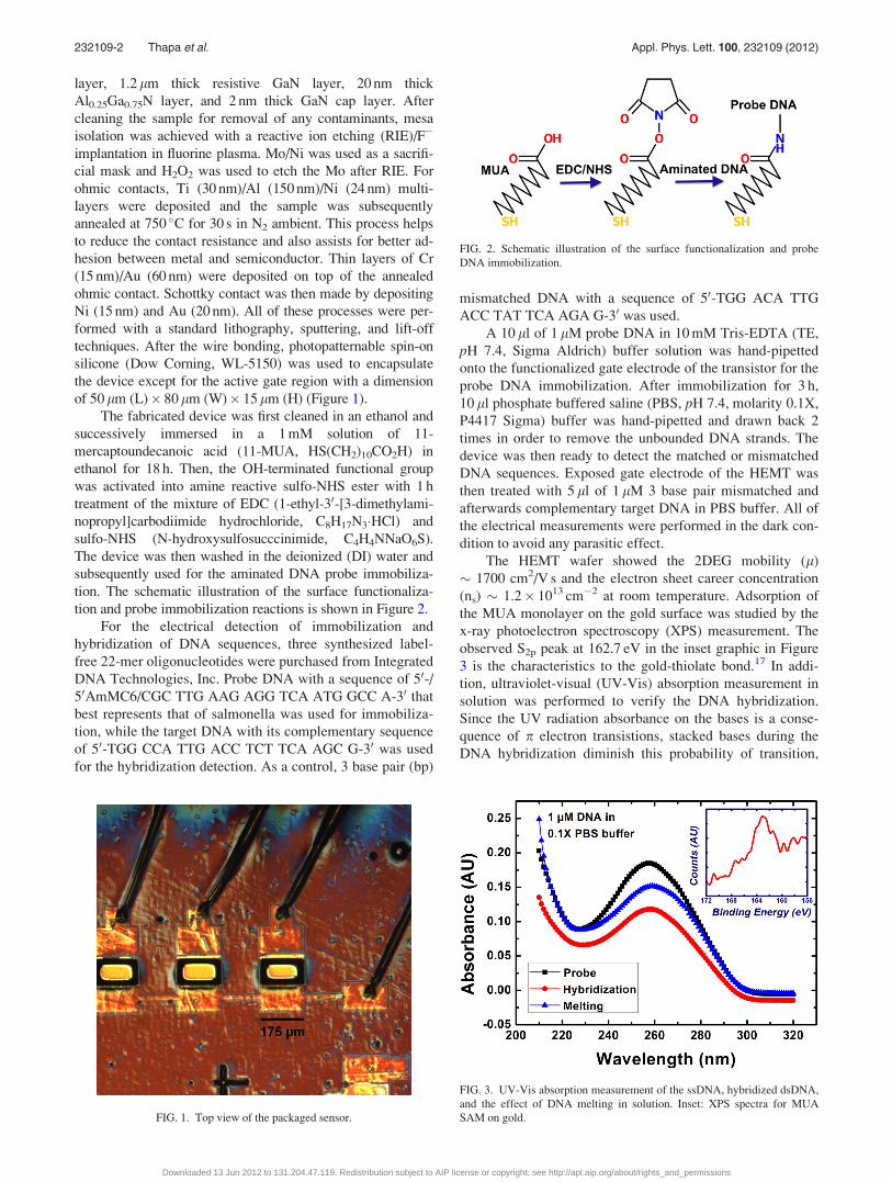
of 50 lm (L)� 80 lm (W)� 15 lm (H) (Figure 1).
The fabricated device was first cleaned in an ethanol and
successively immersed in a 1 mM solution of 11-
mercaptoundecanoic acid (11-MUA, HS(CH2)10CO2H) in
ethanol for 18 h. Then, the OH-terminated functional group
was activated into amine reactive sulfo-NHS ester with 1 h
treatment of the mixture of EDC (1-ethyl-30-[3-dimethylami-
nopropyl]carbodiimide hydrochloride, C8H17N3�HCl) and
sulfo-NHS (N-hydroxysulfosucccinimide, C4H4NNaO6S).
The device was then washed in the deionized (DI) water and
subsequently used for the aminated DNA probe immobiliza-
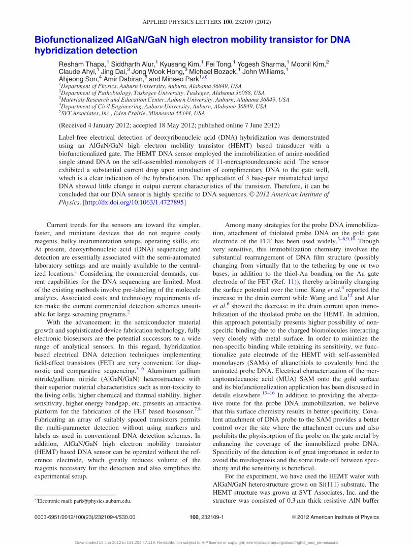
tion. The schematic illustration of the surface functionaliza-
tion and probe immobilization reactions is shown in Figure 2.
For the electrical detection of immobilization and
hybridization of DNA sequences, three synthesized label-
free 22-mer oligonucleotides were purchased from Integrated
DNA Technologies, Inc. Probe DNA with a sequence of 50-/50AmMC6/CGC TTG AAG AGG TCA ATG GCC A-30 that
best represents that of salmonella was used for immobiliza-
tion, while the target DNA with its complementary sequence
of 50-TGG CCA TTG ACC TCT TCA AGC G-30 was used
for the hybridization detection. As a control, 3 base pair (bp)
mismatched DNA with a sequence of 50-TGG ACA TTG
ACC TAT TCA AGA G-30 was used.
A 10 ll of 1 lM probe DNA in 10 mM Tris-EDTA (TE,
pH 7.4, Sigma Aldrich) buffer solution was hand-pipetted
onto the functionalized gate electrode of the transistor for the
probe DNA immobilization. After immobilization for 3 h,
10 ll phosphate buffered saline (PBS, pH 7.4, molarity 0.1X,
P4417 Sigma) buffer was hand-pipetted and drawn back 2
times in order to remove the unbounded DNA strands. The
device was then ready to detect the matched or mismatched
DNA sequences. Exposed gate electrode of the HEMT was
then treated with 5 ll of 1 lM 3 base pair mismatched and
afterwards complementary target DNA in PBS buffer. All of
the electrical measurements were performed in the dark con-
dition to avoid any parasitic effect.
The HEMT wafer showed the 2DEG mobility (l)
� 1700 cm2/V s and the electron sheet career concentration
(ns) � 1.2� 1013 cm�2 at room temperature. Adsorption of
the MUA monolayer on the gold surface was studied by the
x-ray photoelectron spectroscopy (XPS) measurement. The
observed S2p peak at 162.7 eV in the inset graphic in Figure
3 is the characteristics to the gold-thiolate bond.17 In addi-
tion, ultraviolet-visual (UV-Vis) absorption measurement in
solution was performed to verify the DNA hybridization.
Since the UV radiation absorbance on the bases is a conse-
quence of p electron transistions, stacked bases during the
DNA hybridization diminish this probability of transition,
FIG. 1. Top view of the packaged sensor.
FIG. 2. Schematic illustration of the surface functionalization and probe
DNA immobilization.
FIG. 3. UV-Vis absorption measurement of the ssDNA, hybridized dsDNA,
and the effect of DNA melting in solution. Inset: XPS spectra for MUA
SAM on gold.
232109-2 Thapa et al. Appl. Phys. Lett. 100, 232109 (2012)
Downloaded 13 Jun 2012 to 131.204.47.119. Redistribution subject to AIP license or copyright; see http://apl.aip.org/about/rights_and_permissions
reducing absorbance. This effect is known as hypochromic
effect.18 On the other hand, increased temperature disrupts
the hydrogen bond and denatures the DNA duplex. This
unstacking of DNA base pairs results in an increase in the
UV absorbance at 260 nm, which is known as hyperchromic
effect.19 The characteristic maxima near 260 nm in Figure 3
shows the hybridization and denaturation of the DNA strands
depicting corresponding hypochromic and hyperchromic
effects, respectively.
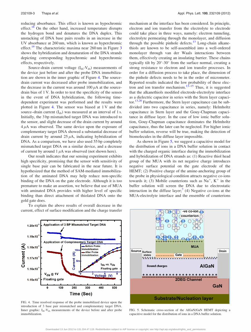
Source-drain current voltage (Ids-Vds) measurements of
the device just before and after the probe DNA immobiliza-
tion are shown in the inner graphic of Figure 4. The source-
drain current was decreased after probe immobilization, and
the decrease in the current was around 100 lA at the source-
drain bias of 1 V. In order to test the specificity of the sensor
in the event of DNA hybridization, the following time-
dependent experiment was performed and the results were
plotted in Figure 4. The sensor was biased at 1 V and the
source–drain current (Ids) was measured at an interval of 1 s.
Initially, the 3 bp mismatched target DNA was introduced to
the sensor, and slight decrease of the drain current by around
4 lA was observed. The same device upon the exposure of
complementary target DNA showed a substantial decrease of
drain current by around 25 lA, indicating hybridization of
DNA. As a comparison, we have also used 55 bp completely
mismatched target DNA on a similar device, and a decrease
of current by around 1 lA was observed (not shown here).
Our result indicates that our sensing experiment exhibits
high specificity, promising that the sensor with sensitivity of
single base pair can be fabricated in the near future. It is
hypothesized that the method of SAM-mediated immobiliza-
tion of the aminated DNA may help reduce non-specific
binding of the DNA on the gate electrode. Although it is too
premature to make an assertion, we believe that use of MUA
with aminated DNA provides with higher level of specific
binding than direct attachment of thiolated DNA onto the
gold gate does.
To explain the above results of overall decrease in the
current, effect of surface modification and the charge transfer
mechanism at the interface has been considered. In principle,
electron and ion transfer from the electrolyte to electrode
could take place in three ways, namely: electron tunneling,
electrolyte permeating through the monolayer, and diffusion
through the possible pinhole defects.13 Long-chain alkane-
thiols are known to be self-assembled into a well-ordered
monolayer through van der Waals interactions between
them, effectively creating an insulating barrier. These chains
typically tilt by 20�-30� from the surface normal, creating a
strong resistance to electron and ion transfer processes. In
order for a diffusion process to take place, the dimension of
the pinhole defects needs to be in the order of micrometer.
Reported results indicated the low probability of these elec-
tron and ion transfer mechanism.13–15 Thus, it is suggested
that the alkanethiols modified electrode-electrolyte interface
as a dielectric capacitor in series with the Stern layer capaci-
tor.13,20 Furthermore, the Stern layer capacitance can be sub-
divided into two capacitance in series, namely: Helmholtz
capacitance in Stern layer and the Gouy-Chapman capaci-
tance in diffuse layer. In the case of low ionic buffer solu-
tion, Gouy-Chapman capacitance dominates the Helmholtz
capacitance, thus the later can be neglected. For higher ionic
buffer solution, reverse will be true, making the detection of
biomolecules in the diffuse layer impossible.
As shown in Figure 5, we suggest a capacitive model for
the distribution of ions in a DNA buffer solution in contact
with the charged organic interface during the immobilization
and hybridization of DNA strands as: (1) Reactive thiol head
group of the MUA with its net negative charge introduces
negative surface potential on the gate electrode of the
HEMT; (2) Positive charge of the amine-anchoring group of
the probe in physiological condition attracts negative co-ions
towards it; (3) Mobile counterions such as Naþ, Kþ in the
buffer solution will screen the DNA due to electrostatic
interaction in the diffuse layer;7 (4) Negative co-ions at the
MUA-electrolyte interface and the ensemble of counterions
FIG. 4. Time resolved response of the probe immobilized device upon the
introduction of 3 base pair mismatched and complementary target DNA.
Inner graphic: Ids-Vds measurements of the device before and after probe
immobilization.
FIG. 5. Schematic cross-section of the AlGaN/GaN HEMT depicting a
capacitive model for the distribution of ions in a DNA buffer solution.
232109-3 Thapa et al. Appl. Phys. Lett. 100, 232109 (2012)
Downloaded 13 Jun 2012 to 131.204.47.119. Redistribution subject to AIP license or copyright; see http://apl.aip.org/about/rights_and_permissions
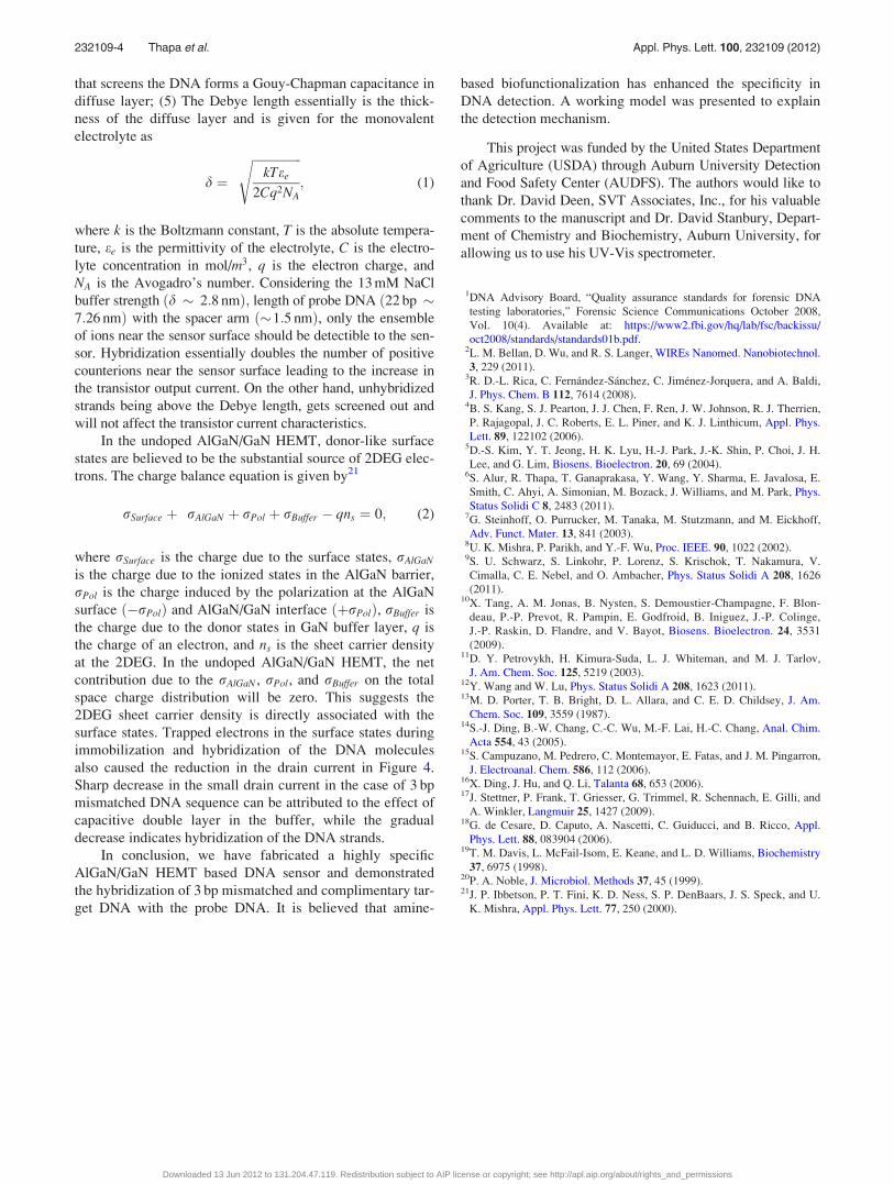
that screens the DNA forms a Gouy-Chapman capacitance in
diffuse layer; (5) The Debye length essentially is the thick-
ness of the diffuse layer and is given for the monovalent
electrolyte as
d ¼ffiffiffiffiffiffiffiffiffiffiffiffiffiffiffiffi
kTee
2Cq2NA
s; (1)
where k is the Boltzmann constant, T is the absolute tempera-
ture, ee is the permittivity of the electrolyte, C is the electro-
lyte concentration in mol/m3, q is the electron charge, and
NA is the Avogadro’s number. Considering the 13 mM NaCl
buffer strength ðd � 2:8 nmÞ; length of probe DNA ð22 bp �7:26 nmÞ with the spacer arm ð�1:5 nmÞ, only the ensemble
of ions near the sensor surface should be detectible to the sen-
sor. Hybridization essentially doubles the number of positive
counterions near the sensor surface leading to the increase in
the transistor output current. On the other hand, unhybridized
strands being above the Debye length, gets screened out and
will not affect the transistor current characteristics.
In the undoped AlGaN/GaN HEMT, donor-like surface
states are believed to be the substantial source of 2DEG elec-
trons. The charge balance equation is given by21
rSurface þ rAlGaN þ rPol þ rBuffer � qns ¼ 0; (2)
where rSurface is the charge due to the surface states, rAlGaN
is the charge due to the ionized states in the AlGaN barrier,
rPol is the charge induced by the polarization at the AlGaN
surface ð�rPolÞ and AlGaN/GaN interface ðþrPolÞ, rBuffer is
the charge due to the donor states in GaN buffer layer, q is
the charge of an electron, and ns is the sheet carrier density
at the 2DEG. In the undoped AlGaN/GaN HEMT, the net
contribution due to the rAlGaN , rPol, and rBuffer on the total
space charge distribution will be zero. This suggests the
2DEG sheet carrier density is directly associated with the
surface states. Trapped electrons in the surface states during
immobilization and hybridization of the DNA molecules
also caused the reduction in the drain current in Figure 4.
Sharp decrease in the small drain current in the case of 3 bp
mismatched DNA sequence can be attributed to the effect of
capacitive double layer in the buffer, while the gradual
decrease indicates hybridization of the DNA strands.
In conclusion, we have fabricated a highly specific
AlGaN/GaN HEMT based DNA sensor and demonstrated
the hybridization of 3 bp mismatched and complimentary tar-
get DNA with the probe DNA. It is believed that amine-
based biofunctionalization has enhanced the specificity in
DNA detection. A working model was presented to explain
the detection mechanism.
This project was funded by the United States Department
of Agriculture (USDA) through Auburn University Detection
and Food Safety Center (AUDFS). The authors would like to
thank Dr. David Deen, SVT Associates, Inc., for his valuable
comments to the manuscript and Dr. David Stanbury, Depart-
ment of Chemistry and Biochemistry, Auburn University, for
allowing us to use his UV-Vis spectrometer.
1DNA Advisory Board, “Quality assurance standards for forensic DNA
testing laboratories,” Forensic Science Communications October 2008,
Vol. 10(4). Available at: https://www2.fbi.gov/hq/lab/fsc/backissu/
oct2008/standards/standards01b.pdf.2L. M. Bellan, D. Wu, and R. S. Langer, WIREs Nanomed. Nanobiotechnol.
3, 229 (2011).3R. D.-L. Rica, C. Fernandez-Sanchez, C. Jimenez-Jorquera, and A. Baldi,
J. Phys. Chem. B 112, 7614 (2008).4B. S. Kang, S. J. Pearton, J. J. Chen, F. Ren, J. W. Johnson, R. J. Therrien,
P. Rajagopal, J. C. Roberts, E. L. Piner, and K. J. Linthicum, Appl. Phys.
Lett. 89, 122102 (2006).5D.-S. Kim, Y. T. Jeong, H. K. Lyu, H.-J. Park, J.-K. Shin, P. Choi, J. H.
Lee, and G. Lim, Biosens. Bioelectron. 20, 69 (2004).6S. Alur, R. Thapa, T. Ganaprakasa, Y. Wang, Y. Sharma, E. Javalosa, E.
Smith, C. Ahyi, A. Simonian, M. Bozack, J. Williams, and M. Park, Phys.
Status Solidi C 8, 2483 (2011).7G. Steinhoff, O. Purrucker, M. Tanaka, M. Stutzmann, and M. Eickhoff,
Adv. Funct. Mater. 13, 841 (2003).8U. K. Mishra, P. Parikh, and Y.-F. Wu, Proc. IEEE. 90, 1022 (2002).9S. U. Schwarz, S. Linkohr, P. Lorenz, S. Krischok, T. Nakamura, V.
Cimalla, C. E. Nebel, and O. Ambacher, Phys. Status Solidi A 208, 1626
(2011).10X. Tang, A. M. Jonas, B. Nysten, S. Demoustier-Champagne, F. Blon-
deau, P.-P. Prevot, R. Pampin, E. Godfroid, B. Iniguez, J.-P. Colinge,
J.-P. Raskin, D. Flandre, and V. Bayot, Biosens. Bioelectron. 24, 3531
(2009).11D. Y. Petrovykh, H. Kimura-Suda, L. J. Whiteman, and M. J. Tarlov,
J. Am. Chem. Soc. 125, 5219 (2003).12Y. Wang and W. Lu, Phys. Status Solidi A 208, 1623 (2011).13M. D. Porter, T. B. Bright, D. L. Allara, and C. E. D. Childsey, J. Am.
Chem. Soc. 109, 3559 (1987).14S.-J. Ding, B.-W. Chang, C.-C. Wu, M.-F. Lai, H.-C. Chang, Anal. Chim.
Acta 554, 43 (2005).15S. Campuzano, M. Pedrero, C. Montemayor, E. Fatas, and J. M. Pingarron,
J. Electroanal. Chem. 586, 112 (2006).16X. Ding, J. Hu, and Q. Li, Talanta 68, 653 (2006).17J. Stettner, P. Frank, T. Griesser, G. Trimmel, R. Schennach, E. Gilli, and
A. Winkler, Langmuir 25, 1427 (2009).18G. de Cesare, D. Caputo, A. Nascetti, C. Guiducci, and B. Ricco, Appl.
Phys. Lett. 88, 083904 (2006).19T. M. Davis, L. McFail-Isom, E. Keane, and L. D. Williams, Biochemistry
37, 6975 (1998).20P. A. Noble, J. Microbiol. Methods 37, 45 (1999).21J. P. Ibbetson, P. T. Fini, K. D. Ness, S. P. DenBaars, J. S. Speck, and U.
K. Mishra, Appl. Phys. Lett. 77, 250 (2000).
232109-4 Thapa et al. Appl. Phys. Lett. 100, 232109 (2012)
Downloaded 13 Jun 2012 to 131.204.47.119. Redistribution subject to AIP license or copyright; see http://apl.aip.org/about/rights_and_permissions