Bio-Data - cecri.res.in · 39 years R&D (Research and development) experience in the field of...
80
- 1 - Bio-Data 1. Name : Dr. M. Jayachandran 2. Date of Birth : 04-02-1954 3. Current position and address : Chief Scientist Head Electrochemical Materials Science Division CSIR-Central Electrochemical Research Institute Karaikudi – 630 006, India Contact details : 91-4565-241539 (Off.) Mobile Number : 0091-9443619470 Fax Number : 91-4565 -227713 Email address : [email protected] [email protected] www.cecri.res.in/mj 4. Educational Qualifications : Degree Subject / Specialization Year University Class Ph.D., Industrial Chemistry 2002 Alagappa University, Karaikudi Commendable M.Sc., Physics 1976 Annamalai University, Chidambaram First B.Sc., Physics 1974 (First Prize) Madurai Kamaraj University, Madurai First 5. Chronological career progression details: Sl. No From To Name of Organization Position held 1. 1983 1988 CSIR - CECRI, Karaikudi Scientist – B 2. 1988 1993 CSIR - CECRI, Karaikudi Scientist – C 3. 1993 1998 CSIR - CECRI, Karaikudi Scientist – EI 4. 1998 2003 CSIR - CECRI, Karaikudi Scientist – EII 5. 2003 2009 CSIR - CECRI, Karaikudi Scientist – F 6. 2009 Till date CSIR - CECRI, Karaikudi Chief Scientist 6. Total Research Experience/Area of Specialization (ANNEXURE-1) 6(a). Research Experience 39 years R&D (Research and development) experience in the field of electrochemical science and technology and Materials Science at CSIR- CECRI, Karaikudi. Classified into three major areas of Research .
Transcript of Bio-Data - cecri.res.in · 39 years R&D (Research and development) experience in the field of...

- 1 -
Bio-Data
1. Name : Dr. M. Jayachandran
2. Date of Birth : 04-02-1954
3. Current position and address : Chief Scientist
Head
Electrochemical Materials Science Division
CSIR-Central Electrochemical Research
Institute
Karaikudi – 630 006, India
Contact details : 91-4565-241539 (Off.)
Mobile Number : 0091-9443619470
Fax Number : 91-4565 -227713
Email address : [email protected]
www.cecri.res.in/mj
4. Educational Qualifications :
Degree Subject /
Specialization
Year University Class
Ph.D., Industrial
Chemistry
2002 Alagappa University,
Karaikudi
Commendable
M.Sc., Physics 1976 Annamalai
University,
Chidambaram
First
B.Sc., Physics 1974
(First Prize)
Madurai Kamaraj
University, Madurai
First
5. Chronological career progression details:
Sl. No From To Name of Organization Position held
1. 1983 1988 CSIR - CECRI, Karaikudi Scientist – B
2. 1988 1993 CSIR - CECRI, Karaikudi Scientist – C
3. 1993 1998 CSIR - CECRI, Karaikudi Scientist – EI
4. 1998 2003 CSIR - CECRI, Karaikudi Scientist – EII
5. 2003 2009 CSIR - CECRI, Karaikudi Scientist – F
6. 2009 Till date CSIR - CECRI, Karaikudi Chief Scientist
6. Total Research Experience/Area of Specialization (ANNEXURE-1)
6(a). Research Experience
39 years R&D (Research and development) experience in the field of
electrochemical science and technology and Materials Science at CSIR-
CECRI, Karaikudi. Classified into three major areas of Research .

- 2 -
6(b). Field of specialisation
Research experience in Physical Chemistry, Electrochemical Materials
Science & Nanotechnology.
Preparation of nano crystalline metal oxide and composite
powders/films using Electrochemical, chemical, sol-gel and combustion
synthesis routes for gas sensors and catalysis for waste effluent
treatment.
Deposition of metal oxide thin films using various physical, vacuum and
sputtering, electro chemical, pulsed laser techniques useful for solid
state, Photo Electrochemical and dye sensitized solar cells.
Characterization of physical and Chemical, Electrochemical properties
of Nano semiconductor powders/hard coatings/metal oxide films (XRD,
TEM, XPS, AFM, SEM, FTIR, Raman shift, NMR, ESR, Uv-Vis,
Electrochemical impedance characterization techniques).
Societal Mission Solar Energy projects: Solar Street lights in villages,
Solar power plants, Awareness programmes
7. Research and Development Activities
7(a). Research Publications and Patents (Details given in Annexures separately)
Research Papers in International SCI Journals/National/Scopus: 220 Annexure– II
Papers presented in Conference/Published in Proceedings : 68 Annexure– III
Honors, Awards, Fellowship, Editorship received : 28 Annexure– IV
National /International events organized as Co-ordinator /
National Organizing Committee Member : 09 Annexure– V
7(b). Graduation/Inaugural/Validictory Addresses, Invited talk / Plenary
Lectures delivered
Talks on Solar Energy / Nano materials/devices/Hard coatings
/Thin film and preparation techniques/characterisation techniques/addresses
in Engineering/Arts & Science colleges/Universities : 72
7(c). Dissertations supervised Total: 101
M.Phil.,(Physics) : 37
M.Sc., (Physics) : 23
M.Sc., (Chemistry) : 07
M.Sc.,(Industrial chemistry) : 01
M.Sc., (Materials Science & Technology) : 09
M.Tech., (Electronics) : 01
M.Tech., (Nanoscience) : 04
M.Tech., (Mechanical) : 02
B.Tech., (Chemical & Electrochemical Engineering) : 04
M.E. ( Materials Science) : 01
B.E. (Bachelor of Engineering) EIE, IT, CSE : 12

- 3 -
8. Contribution to CFE (B.Tech course) CECRI, AcSIR, Academic Institutions
8(a). Contribution to CFE (B.Tech course) CECRI, AcSIR
Handled Physics Classes and Labs.
8(b). Contribution as Board of studies member/Ph.D. evaluation in academic
institutions (Science/Engineering Colleges and Universities of
Tamilnadu)
Sl.No. Year Role Institution
1. 2015-2013 Member Board of Adjudicators for Ph.D., and
M.Phil.,Avinashilingam University for
Women, Coimbatore
2. 2014-2010 Member Board of Adjudicators for Ph.D.,
Thiruvananthapuram, University of Kerala,
Kerala
3. 2015-2013 Member Acadamic Council, Sethu Institute of
Technology, Kariapatti, Madurai, Tamilnadu
4. 2013-2010 Member Ph.D. evaluation committee, Bharathiyar
University, Coimbatore, Tamilnadu
5. 2012 Member Ph.D. evaluation committee, Madurai
Kamaraj University, Madurai, Tamilnadu
6. 2011 Member Ph.D. evaluation committee. Anna University
of Technology, Thiruchirapalli, Tamilnadu
7. 2012-2011 Member Research Advisory Committee, Sethu
Institute of Technology, Kariapatti, Madurai,
Tamilnadu
8. 2009-2008 Member Board of studies, Sri Nandhanam college of
Engineering, Tiruppatur, Tamilnadu.
9. 2008 – 2006 Member Board of studies, M.Sc (Post Graduate)
Physics, Bishop Heber College, Trichy,
Tamilnadu.
10. 2006 – 2005 Member Board of studies, B.Tech. (Bachelor of
Technology) School of Engineering and
Technology, Bharathidasan University,
Trichy, Tamilnadu.
11. 2006 – 2004 Member Board of studies, M.Sc (Post Graduate)
Materials Science & Technology, Thiagarajar
College of Engineering, Madurai, Tamilnadu.
12. 2006 – 2004 Member Board of studies, M.Sc (Post Graduate)
Physics, Bishop Heber College, Trichy,
Tamilnadu.
13. 2002 – 2000 Member Board of studies, M.Sc (Post Graduate)
Materials Science & Technology, Thiagarajar
College of Engineering, Madurai, Tamilnadu.

- 4 -
9. Administrative/Organizational Contributions in CSIR-CECRI, Karaikudi.
9(a). Administrative Affiliation in CECRI
No. Year Role Committee
1. till date -
October 2014
Acting
Director
2. 2015-2012 Chairman ERP implementation Committee
3. March 2013-
October 2012
Acting
Director
4. 2015 -2011 Member CECRI Administrative collegium
5. 2015-2011 Chairman Funding/Monitoring Start-up Projects for
Young scientists/QHS/Inter divisional
Projects
6. 2015-2011 Member Empower Committee
7. 2014-2012 Member Consultative Mechanism for redressal of
the employees grievances at the Institute
level
8. 2015-2001 Liaison
Officer
for OBC
CECRI, Karaikudi
9. 2013-2012 Chairman CECRI Website validation Committee
10. 2013-2012 Chairman Compassionate Appointment Committee
11. 2014-2012 Chairman Guest House Management Committee
12. 2013-2012 Member Lab Level Task Force Committee
13. 2013-2012 Chairman Lab Level Implementation Team
14. March 2013-
October 2012
Vice-
President
CECRI Staff Club
15. 2012-2011 Chairman Outstanding Balance (OB) Clearance
Committee
16. 2010-2009 Member Local Grievances Committee
17. 2007-2004 Chairman Dept. Canteen Management Committee,
CECRI
18. 2005-2003 Member Library Committee
19. 2004-2002 Member Outstanding Balance (OB) Clearance
Committee
20. 2000-1998 Secretary CECRI Staff Club
21. 1999-1998 Member CSIR Foundation day organizing
Committee
22. 1988-1986 Secretary Dept. Canteen Management Committee,
CECRI
(9b). Contribution as Chairman/Nominee/Member in S&T Organizational
Committees in CECRI, Karaikudi
1. 2015, 2014 Directors’ Recruitment & Assessment Board (RAB)

- 5 -
Nominee Selection Committee, CSIR
2. 2015-2012 Chairman 140 kw Solar Power Plant Committee
3. 2013-2012 Directors’
Nominee
Scientist Selection Committee, CECRI
4. 2013-2012 Chairman Project Assistant Selection Committee
5. 2013-2012 Member Medical Officer Selection Committee
6. 2013-2012 Chairman Apprentice Selection Committee
7. 2013-2012 Chairman Anti ragging Committee for Centre For Education
(CFE)
8. 2011-2010 Member Quick Hire Fellow Selection committee
9. 2010-2009 Member Project Monitoring committee, CECRI
10. 2010-2009 Member Prioritization committee for Procurement of
Equipments,
11. 2010-2008 Member Scientist Selection Committees (B,C & EI),
CECRI
12. 2007 Member Screening committee for recruitment &
assessment promotion of scientists
13. 2007 Directors’
Nominee
Assessment committee for Technical staff
14. 2007-1998 Member
Various Recruitment Committees for project
staffs/ Apprentices
15. 2003-2000 Member Deputation Committee for Seminars/ Training/
Foreign
16. 2002 Member Committee to Prioritize In-house projects
17. 2002 Member Assessment Committee for Group II Staff
18. 2002 Member Selection Committee for LDC under casual
workers absorption scheme of CSIR
19. 2002-1998 Member Standing Committee for Technical Service
20. 2002-1998 Member Stores Committee
10. Professional Membership in Scientific Societies
1. . 2005 Life Member
(LM – 122)
Electrochemical Society of India (ECSI),
Bangalore, India
2. 2004 Life Member
(LM – 48)
Indian Society for Electroanalytical Chem.
(ISEAC), BARC, Mumbai.
3. 2003 Life Member
(LM – 1096)
Instrument Society of India, Bangalore
4. 2000 Life Member
(LM – 225)
Indian Thermal Analysis Society, BARC Mumbai.
5. 2000 Life Member
(LM – B314)
Materials Research Society of India, Bangalore
6. 1997 Life Member
(LM – 0727)
Solar Energy Society of India, New Delhi.
7. 1995 Life Member
(LF – 412)
Society for Advancement of Electrochemical
Science and Technology (SAEST), Karaikudi.

- 6 -
11. Total Career Profile:- Major Research Projects ongoing and completed
Funding received from
Council of Scientific and Industrial Research (CSIR), New Delhi
Board of Research in Nuclear Sciences (BRNS), Mumbai
Department of Science and Technology (DST), New Delhi
All India Council for Technical Education (AICTE), New Delhi
Presently involved R&D Ongoing projects:
11.1. CSC0134-CSIR- 12th FYP Project, New Delhi: Co- Investigator:
Development of bioactive glassy metals coated implants and
antimicrobial active immobilized fabrics for human healthcare (M2D),
2012 – 2017 (Rs. 1.66 Crores) Objectives: To develop Zirconium based glassy metals of Zr–Cu–Ag–Al
systems by reactive magnetron sputtering and Pulsed laser deposition which
would be applied on the surfaces of bio medical implants made of stainless
steel (AISI 316L), titanium and titanium alloys (Ti-6Al-4V) and to investigate
the microstructural, mechanical properties. In vitro bio corrosion studies will
be done using SVET, DC polarization and AC impedance. Biocompatibility
will be evaluated by thrombogenecity and cytotoxicity studies. Synthesis of
inorganic nano-particles and their nano-composites as anti-microbial agents to
prevent undesirable effects such as degradation, staining and deterioration of
fibers in textiles. A wide range of nanoparticles with various structures will be
immobilized on the fibers, which will bring new and medicinal properties to
the final textile product.
The following inorganic nano-structured anti-microbial agents will be studied:
TiO2 nano-particles, Metallic and non-metallic TiO2 nano-composites, Titania
nanotubes (TNTs), Zinc oxide nano-particles and nano-rods, Copper oxide
nano-particles. Techniques such as sol-gel method, electrospinning, chemical
and photocatalytic reduction process, sonochemical irradiation and magnetron
sputtering will be used. The antibacterial activities of the nano-structured
materials will be tested against Escherichia coli (Gram negative) and
Staphylococcus aureus (Gram positive) cultures. Zr48Cu36Al8Ag8 (at.%) thin
film metallic glasses were deposited on 316L stainless steel substrates by
magnetron sputtering as thin homogeneous layers. Potentiodynamic
polarization and AC impedance analysis in SBF showed that the as sputtered
Zr48Cu36Al8Ag8 on 316L SS specimen had higher corrosion resistance without
any localized pitting compared to the crystalline base alloy.
11.2. CSC 0101-12th FYP Project - CSIR- Network Project, New Delhi: Member
with Corrosion Group: Corrosion and monitoring structures: Smart
sensors and on-line monitoring (MULTIFUN), 2012 - 2017 (Rs. 2.00
Crores) Metallic Oxide coated cylindrical and flat plate sensor electrodes have been
prepared with various thickness. Their corrosion related parameters and
sensing behavior in concrete structures will be studied. Sensors are to be
embedded in concrete structures and multifunctional parameters such as half-

- 7 -
cell potential, chloride level, resistivity, alkalinity and corrosion rate of
reinforcements to be monitored. The integrated sensor along with online
monitoring sensor platform to be the expected outcome of the project.
11.3. GAP–17/12-Department of Atomic Energy, BRNS, Mumbai: Co-
Investigator :- Development of nanocomposite Ti-X-N (where X=B, Si, V, C
and Cr) coatings by pulsed magnetron sputtering for multiple applications,
2012 – 2015. Rs. 23.908 Lakhs)
The main objective is to prepare the transition metal nitride composite
coatings such as Ti–X–N (where X=B, Si, V, C and Cr) by reactive pulsed
magnetron sputtering after optimizing the process parameters such as substrate
temperature, pressure, power, Ar/N2 flow rate variation etc. The structural
properties of these coatings will be studied in detail. The mechanical strength
of the coatings will be tested by measuring hardness, adhesion and abrasion
wear. Scanning Vibrating Electrode Technique (SVET) will be used to
investigate localized electrochemistry and corrosion phenomena
Electrochemical Noise (EN) measurements Microstructure of the coatings will
be studied before and after the corrosion tests.
Chromium nitride films were coated on D9 steel substrates by reactive DC
magnetron sputtering process. The XRD pattern confirmed the grown films
have polycrystalline nature and exhibited CrN and Cr2N phases. The coated
D9 steel showed higher charge transfer resistance values compared to bare
substrate. The corrosion current density (Icorr) was found to decrease from 1.31
x10-7A for bare substrate to 1.88 x 10⁻⁸ A for CrN coated D9 steel specimen. A
decrease in the porosity value was noticed for coated substrate. The
polarisation resistance was found to be higher for the coated specimens. From
electrochemical noise analysis, the current transient was found to decrease
with increasing the immersion time for CrN coated substrate and potential
noise shifted to the positive direction. The noise resistance was found to be
higher for coated specimen than bare substrate.
-7.00E-07
-3.00E-07
1.00E-07
5.00E-07
0 500 1000 1500 2000
Time (s)
Cu
rre
nt
(A)
(c)
(a)
(b)
0.00E+00
4.00E+05
8.00E+05
1.20E+06
1.60E+06
0 500 1000 1500 2000 2500
Immersion time (s)
No
ise
re
sis
tan
ce
(o
hm
)
D9
Cr/D9
CrN/D9
Current noise as a function of time of Noise resistance as a function of immersion
(a) D9 steel (b) Cr/D9 (c) CrN/D9. time for the blank D9 steel, Cr/D9 and CrN/D9
11.4. GAP-03/12-MNRE-Network Project, New Delhi: Co Investi-gator:-Dye-
Sensitize and Quantum Dot Sensitized Solar Cells (DSSC, QDSSC) (TAP-
SUN), 2012-2017 (Rs. 2.036 Crores)

- 8 -
Optimization of the process parameters of titanium dioxide (TiO2), Zinc Oxide
using magnetron sputtering is performed. Titanium dioxide (TiO2) thin films
as block layers are prepared by DC reactive magnetron sputtering at a
substrate temperature of 450°C. X-ray diffraction (XRD) and TEM-(SAED)
analyses of the films reveal that they are polycrystalline in nature and have
tetragonal structure with preferred orientation along the (101) direction. The
presence of characteristic Raman peaks is observed along 173, 200, 400, 517,
640 cm-1 corresponding to anatase structure.
TEM-SAED Pattern of TiO2 Raman spectrum for TiO2 block layer
The surface morphological studies by FESEM, AFM reveal the uniform
surface coverage of the grains on the surface of the films. An optical
transmittance value of 80% in the visible light region with the optical band
gap value of 3.2 eV is measured. These sputtered TiO2 thin film is used as
blocking layer over which thick layer of TiO2 of about 10µm is prepared using
TiO2 paste and this stack is used as photoanode of DSSC cell. Electron beam
evaporated platinum thin film on FTO coated glass substrate is used as counter
electrode. The cell stack is shown below. The performance of the cell with an
efficiency of 4.15% is achieved.
Representative DSSC stacks
The dye-sensitized photoelectrodes with block layers displayed improved Voc
and Jsc without lowering the FF, which improved the device performance.
Studies are underway to further enhance the performance of DSSCs that
include a compact nitrogen doped TiO2 layer using newly developed working
electrode, and a report will be forthcoming.
R&D/Consultancy Projects Completed
11.5. NWP–10-CSIR-Network Project, New Delhi:CECRI Co-ordinator:
Development of Speciality inorganic materials for diverse applications,
2007 – 2012 (Rs.1.185 Crores)
Oxide semiconductor thin films with nanostructure, as porous silicon matrix,
transition metal oxides in thin film form and in powder were developed,
through chemical routes. Various techniques such as RF sputtering, electron
beam evaporation, electrochemical techniques, spray pyrolysis, were engaged

- 9 -
for device development like; gas sensors, electrochromic windows,
photoluminescent devices and batteries.
Important achievements:
Chemically stable and highly crystalline MgIn2O4 films was prepared using
spray pyrolysis deposition technique on quartz substrate.Low resistivity NiO
films, possessing anodic electrochromic properties, was deposited by the
electron beam evaportation technique.Titanium nitride(TiN) films were
deposited on AISI 316L stainless steel substrate by reactive magnetron
sputtering using a Ti target. Corrosion resistance and hemocompatibility of
TiN coated AISI 316L SS were studied for clinical applications.Deposition of
nanocrystalline Indium TinOxide (ITO) was carried out using Radio frequency
(RF) sputtering and spray pyrolysis technique.
Fabrication of Next generation TiO2-Lithium ion batteries:
Recently TiO2 based materials have also been demonstrated as potential anode
material in rechargeable lithium ion batteries. TiO2 has a lithium insertion
voltage around 1.5 V which is far above the lithium plating voltage thus
leading to safer lithium (/-ion) batteries when compared to carbonaceous
materials. Also of importance TiO2 is chemically stable, environmentally
benign and low effective cost. By virtue of its exceptionally fast Li insertion
and extraction kinetics, TiO2- based materials (anatase) have drawn the
research interest as anode materials for next-generation lithium ion batteries.
Charge- discharge curves of TiO2 electrode at different conditions
The potential plateaus at 1.73 and 1.88V correspond to Li-ion insertion into
and extraction from the interstitial octahedral sites of the TiO2 nanotubes, and
these Li ions are easily reversible. The lithium insertion/ extraction reaction in
TiO2 electrode can be written as
LixTiO2 ↔ xLi+ +x e- +TiO2
The maximum value of the insertion coefficient x has been determined to be
about 0.5 that corresponds to a theoretical capacity of 167 mAh g-1. Figure
shows the charge- discharge curves of TiO2 electrode at C/10, C/5 and C-rates.
0 5 10 15 20 25 30 35 40 45 500
20
40
60
80
100
120
140
160
TiO2_FS_450
C
1C
C/5
C/10
Sp
ecif
ic C
ap
aci
ty (
mA
hg
-1)
Cycle number
Charge
Discharge

- 10 -
11.6. GAP 19/08- DST project, New Delhi: Dy. Project Co-ordinator:-
Development of Nanoscale Multilayered and nano composite super hard
coatings by reactive magnetron sputtering for biomedical applications,
2009–2011 (Rs. 14.00 lakhs)
The structural, mechanical, corrosion properties and biocompatibility of
TiN/TiAlN, TiN/NbN, TiN/VN multilayer and Ti-Si-N nanocomposite coatings
prepared by reactive dc magnetron sputtering in an Ar-N2 gas mixture was
studied. Morphological study showed uniform coatings with columnar surface
morphology.
The characteristic peaks were observed from Laser Raman spectrum of Ti-Si-
N. The lower friction coefficient and wear rate observed for the multilayer
coated sample indicated that the better wear resistance.
A maximum hardness value of 39GPa was observed for Ti-Si-N.Multilayer
coatings and had better hemocompatability than single layer and bare AISI
316LSS substrates. The attachment of bacteria on multilayer coatings was
found to be very minimum and without colonization. The multilayer coated
316L surfaces showed a significant reduction of the presence of bacteria, and
this fact could probably be important in the decrease of the inflammation of the
peri-implant soft tissues. It is concluded that by using the transition metal
nitride based multilayer coated 316L SS as a human body implant,
improvement of corrosion resistance as an indication of biocompatibility could
be obtained.
11.7. GAP 19/06- Department of Atomic Energy, BRNS, Mumbai: Dy. Project
Co-ordinator:-Development of Magnetron Sputtered Transition Metal
nitride coatings (CrN, ZrN, AlN) and evaluation of their structural,
mechanical and corrosion properties, 2006–2009) (Rs.13.39 Lakhs)
Hard coating of transition metal nitrides was developed by magnetron
sputtering technique to have high mechanical strength and high corrosion
resistance.
11.8. DU 10 OLP 0038-CSIR-Non-net work Project, New Delhi: Member:-Solar
Battery- Research, Development and Demonstration of Prudent Lead-acid
batteries for solar photovoltaic stand alone systems, 2005-2007 (Rs.25.00
Lakhs)
At present, solar lighting systems employ LMLA lead-acid batteries to store the
electrical energy during daytime, which is retrieved on demand during night.
These batteries have poor energy densities and are prone to
sulphonation/stratification due to the large electrolyte volume. Besides, these
batteries require periodic maintenance. Hence, new type of batteries like,
VRLA-AGM, VRLA-GEL and Hybrid-AGM/GEL-VRLA batteries were
assembled and tested with the objective to develop the most prudent
maintenance-free solar lighting system.
11.9. SSP 11/05-Alagappa University, Karaikudi: Project Co-ordinator:- Spin
coater- pulse console, 2005–2007,(Rs.3.5 lakhs)

- 11 -
Computer controlled spin coating unit and a pulse console was fabricated to
make semiconductor thin films. Spin coater unit can be used for making oxide
thin films using sol-gel precursors. Pulse console can be used to electrodeposit
semiconductor films by using ON and OFF pulses of varying current density.
11.10.Task Force 1C-Net work Project, New Delhi: Group Co-ordinator:
Development of different semiconductor nanoclusters like oxides,
chalcogenides etc.,doped glassy films, 2002-2007 (Rs.85.00 Lakhs)
WO3, MoO3, SnO2, In2O3 oxide films and their ternary compounds were
prepared by the electrochemical, spray pyrolysis, vacuum evaporation and
electron beam evaporation techniques for electrochromic devices and for use
as transparent electrodes. Porous silicon (PSi) structure with nano Si pillars
was formed on P-Si wafer by electrochemical route.
11.11.GAP 20/00)-DST project, New Delhi-Dy.Principal Investigator: Surface
Chemistry and Electronic structure of impurity doped nanocrystals,
2001-2003 (Rs.8.88 Lakhs)
SrAl2O4:Eu2+, Dy3+ phosphors were synthesized using the solid state reaction
of Sr, Al, Eu and Dy carbonates/oxides taken in desired molar
ratio.ZnS:xMn2+ & ZnS:xTb3+ nanoparticle powders were prepared by sol-
gel and combustion synthesis routes.
11.12.GAP 02/00-AICTE project, New Delhi-Member:-Material Preparation and
characterization of Cu and Cr substituted Mn spinels for lithium based
batteries, 2000-2002 (Rs.9.00 Lakhs)
Copper, Chromium, cobalt and zinc substituted spinel were synthesized by
solid state reaction and sol gel methods. The powders were characterized by
XRD, FTIR, DTA, TGA, SEM and impedance studies.
11.13.GAP 15/96-DST project, New Delhi-Dy. Principal Investigator:-
Fundamental and developmental studies on transparent oxide
conductors, 1997-2000 (Rs.6.01 Lakhs)
MgIn2O4, MgSnO3 and MgSn2O4 powders and thin films were prepared by
different routes and their opto electronic properties were studied. Thin films of
MgIn2O4 were also prepared by oxidizing evaporated Mg+In alloy.MgIn2O4
have been synthesized adopting different precursor routes by solid state
reaction. Indates of Mg, Cd and Zn were synthesized both by solid state
reaction route (SSR) and combustion synthesis. Zinc gallate was synthesized
by SSR, Combustion synthesis (CS) and sol-gel routes. Monophase powders
could be obtained only by SSR and CS only. ZnGa2O4 and MgIn2O4 have very
high potentiality as transparent conducting oxide materials in electronic
industries
11.14.SSP 12/99-AICTE Collaborative project with Alagappa University,
Karaikudi Dy.Principal Collaborator–Material preparation and
characterization of layered semiconductor thin film for solar cells, 1999-
2000 (Rs.2.45 Lakhs)
Principal Collaborator :- (CNP 0999) (Rs.0.90 Lakhs)

- 12 -
Sn (S, Se) is a layered compound semiconductor. It is also a very good
material for solar energy conversion. These materials were prepared in the
form of thin film through electrodeposition techniques.
11.15. CNP 05/11–“Advice on Sputter Coating of Titanium Nitride onto Nickel
or Chrome Plated Stainless Steel Needles” to Nano Marker’s Trichy,
2012 (Rs.1.08 Lakhs)
In this consultancy work, initially we did some feasibility studies on sputter
coating of Titanium Nitride on needles and blades made of stainless steel and
mild steel by optimizing the process parameters. After the satisfactory results,
we have advised Nano Marker’s Trichy to purchase DC Magnetron sputtering
facility with the complete required specifications. A DC magnetron sputtering
equipment with a 4” dia cathode assembly was purchased from VR
Technologies, Bangalore and installed it at Nano Marker’s Trichy. We
performed few experiments in front of the client and trained them. Thereafter,
we have made few visits to their company and discussed with them on the
results of the experiments. They are advised to use the equipment for doing
other coatings such as Silver, Sn, Chromium, Copper and Brass. It is
understood from the discussion that they are able to fabricate successfully
these coatings now. The work has been completed to the satisfaction of the
client. The photographs of the products are shown here.
TiN coated needles TiN coated blades
12. Societal Mission Projects received from Government of Tamilnadu for
Non-Conventional Energy and Popularization
Conducted awareness program on utilization of solar energy. Solar lighting
systems were installed in many villages of Ramanathapuram, Pudukottai and
Sivaganga districts. Hands- on training and motivation programs were
conducted for panchayat officials, village people, and students from schools,
polytechnic and engineering colleges.
12.1. SSP 20/01-Solar Project, TN State Govt.–Project Co-ordinator: Design,
Fabrication and Installation of Solar powered street lights in village
panchayats of Pudukkottai Districts, 2002 - 2005, (Rs.14.26 Lakhs)
Solar street lighting systems have been installed in various panchayats.
Training was given to the village youths and women in the self help groups for
the maintenance of batteries, solar panel and control systems. Non-
conventional energy awareness programs were conducted for the village
people, students and panchayat officials.

- 13 -
12.2. SSP 06/06-TN State Government Project: Project Co-ordinator:
Installation of solar lighting systems and conducting hands-on training
programmes for village youths and women self help groups of Sivaganga
Dt. 2006–2008, (Rs.1.40 Lakhs)
Solar street lighting systems have been installed in Aranmanaippatti
panchayat. Training will be given to the village youths and women in the self
help groups for the maintenance of batteries, solar panel and control systems.
Non-conventional awareness programs will be conducted for the village
people, students and panchayat officials.
12.3. CNP 0108-TN State Government Project: Project Co-ordinator:
Installation of solar street lights to Anna Marumalarchi Thittam in
villages in Ramnad district, Practical classes and maintenance, 2001-2003
(Rs.5.952 Lakhs)
Solar street lighting systems have been installed in various panchayats of
Ramnad District. Training was given to the village youths and women in the
self help groups for the maintenance of batteries, solar panel and control
systems.
12.4. CNP 0136-TN State Government Project:Project Co-ordinator:-
Installation of solar lamp systems in Collector’s Camp Office at
Pudukkottai, maintenance & providing training, 2002-2003, (Rs.1.55
Lakhs)
Solar street lighting systems have been installed in Collector’s Camp Office at
Pudukkottai.
12.5. SSP 06/03-TN State Government Project:Project Co-ordinator:- Design,
Fabrication and Installation of Solar street lights and home lighting
systems in woman sanitary complex and self help group buildings in the
habitation of village panchayats in Pudukkottai District, 2003 – 2005,
(Rs. 7.31 lakhs)
Solar street lights were installed in various villages and training programme
for maintenance of batteries and solar panels.
12.6. CNP 0130-TN State Government Project: Project Co-ordinator:-
Fabrication and installation of solar street lights to Singuvalaikurichi
village in Ramnad district, Training & maintenance, 2002 – 2003 (Rs.0.93
Lakh)
Solar street lighting systems were installed in Singuvalaikurichi village in
Ramnad district. Training was given to the village youths and women in the
self help groups for the maintenance of batteries, solar panel and control
systems. Non-conventional energy awareness programs were conducted in the
Village.
12.7. GAP 13/03-Skill Development Training programme, Department of Science
& Technology: Co-ordinator:- 2005- 2006 (Rs.2.00 Lakhs)

- 14 -
Training programme are trained for the un-employed women and men for
repair of cell phones, TVs, CVDs etc so that they can be self-employed to earn
their living.
13. List of Nineteen Best papers published in last 5 years
1. Well-Aligned Graphene Oxide Nanosheets Decorated with zinc Oxide
Nanocrystals for High Performance Photocatalytic Application, K.
Kaviyarasu, C. Maria Magdalane, E. Manikandan, M. Jayachandran, R.
Ladchumananandasivam, S. Neelamani, M. Maaza, International Journal of
Nanoscience Vol. 14, No.3 (2015) 1550007 (8 pages).
2. Antimicrobial activity of sputtered nanocrystalline CuO impregnated fabrics,
B. Subramanian*, K. Anu Priya, S. Thanka Rajan, P.Dhandapani, M.
Jayachandran, Materials Letters 128 (2014) 1-4.
3. 3D Hierarchically assembled porous wrinkled paper-
like structure of ZnCo2O4 and Co-ZnO@C as anode materials for lithium-ion
batteries. Giri Arnab, Pal Provas, A. Ramadoss, M. Jayachandran Mahanty
sourindra, A. Panda, Crystal Growth and Design, Cg-2014-00282n. (2014)
4. Studies of calcium-precipitating oral bacterial adhesionon TiN, TiO2 single
layer, and TiN/TiO2 multilayer- coated 316L SS, G. S.Kaliaraj, A.Ramadass,
M.Sundaram, B.Ssubramanian, M.Jayachandran, J. Master. Sci, DOI
10.1007/s10853-014-8425-7 (2014).
5. Organic Free Low Temperature direct Synthesis of Hierarchical Protonated
layered Titanates/anatase TiO2 hollow spheres and their task specific
applications, Narottam Sutradhar, Sandip Kumar Pahari, Muthirulandi
Jayachandran, A Manuel stephan, J.R.Nair, Balasubramanian Subramanian,
Hari.C.Bajaj, Haresh M, Journal of Materials Chemistry A1 (2013) 9122-
9131
6. CeO2 nanowires with high aspect ratio and excellent catalytic activity for
selective oxidation of styrene by molecular oxygen, Provas Pal, Sandip Kumar
Pahari, Apurba Sinhamahapatra, Muthirulandi Jayachandran, G.V.
Manohar Kiruthika, Hari C. Bajaj, Asit Baran Panda, RSC Advances 3(2013)
10837-10847.
7. Suitability evaluation of plasma ion beam sputtered TiN/TiOxNy multilayers
on steel for bio implants, B. Subramanian, R. Ananthakumar, S.
Yugeswaran,M. Jayachandran, M. Takahashi, Akira Kobayashi., Vacuum 88
(2013) 108-113
8. Facile fabrication of dye-sensitized solar cells utilizing carbon nanotubes
grown over 2D hexagonal bimetallic ordered mesoporous materials, J.
Balamurugan, Thangamuthu, A.Pandurangan, M.Jayachandran, J.Power
Sources 225 (2013) 364-373.
9. Shape-selective synthesis of non-micellar cobalt oxide (CoO) nanomaterials
by microwave irradiations. Subrata Kundu, M. Jayachandran, J. Nanopart
Res 15(4) (2013) 1-13
10. Fabrication of amorphous Zr48Cu36Al8Ag8 thin films by ion beam sputtering
and their corrosion behavior in SBF for bio implants. B. Subramanian, S.
Yugeswaran, Akira Kobayashi, M.Jayachandran, Journal of Alloys and
Compounds 572(2013)163-169.

- 15 -
11. Formation of shape-selective magnetic cobalt oxide nanowires: environmental
application in catalysis studies. Subrata Kundu, M. D. Mukadam, S. M.
Yusuf,M. Jayachandran, Cryst. Eng Comm, 15 (2013) 482-497.
12. Fabrication of Catalytically active nanocrystalline samarium (Sm)-doped
cerium oxide (CeO2) thin films using electron beam evaporation. Subrata
Kundu, Narottam Sutradhar, R. Thangamuthu, B. Subramanian,Asit Baran
Panda, M. Jayachandran, J. Nanopart. Res 14 (2012) 1040
13. Bio synthesis of calcium hydroxyl apatite coating on sputtered Ti/TiN nano
multi layers and their corrosion behavior in simulated bodily solution.
B.Subramanian,P.Dhandapani, S.Maruthamuthu and M.Jayachandran,
Journal of Biomat. Applications 26 (2012) 687-705
14. Nanocomposite Ti-Si-N coatings deposited by reactive dc Magnetron
sputtering for biomedical applications. B.Subramanian, R.Ananthakumar,
Akira Kobayashi and M.Jayachandran. J. American Ceramic Society 205
(2012) 5014.
15. Facile Low-Temperatu re Synthesis of Ceria and Samarium-Doped Ceria
Nanoparticles and Catalytic Allylic Oxidation of Cyclohexene. Sutradhar,
A.Sinhamahapatra, SK.Pahari, M.Jayachandran, B.Subramanian, HC.Bajaj,
A.B.Panda., Journal of Physical Chemistry C 115 (2011) 7628–7637.
16. Structural and tribological properties of DC reactive magnetron sputtered
titanium/titanium nitride (Ti/TiN) multilayered coatings. B. Subramanian,
R.Ananthakumar,M.Jayachandran, Surface & Coatings Technology 205
(2011) 3485–3492
17. Review of material properties of (Mo/W)Se2-layered compound
semiconductors useful for photoelectrochemical solar cells.
S.M.Delphine,M.Jayachandran, C.Sanjeeviraja., Current Applied Physics 11
(2011) 43-49
18. Magnesium Indium Oxide (MgIn2O4)spinel thin films: chemical spray
pyrolysis (CSP) growth and materials characterizations. A. Moses Ezhil Raj,
G. Selvan, M.Jayachandran, C.Sanjeeviraja., J. of Colloid and Interface
Science.328 (2008) 396-401
19. High temperature grown transition metal oxide thin films tuning physical
properties by MeV N+ -ion bombardment R.Sivakumar, C.Saneeviraja,
M.Jayachandran, R.Gopalakrishnan, S.N.Sarangi, D.Paramanik, T.Som,
J.Phys.D:Appl.Phys.41 (2008) art. No.125304 467 – 473.
14. Editor of National Workshop Books/Proceedings:
1. Principles and practice of Powder X-ray Diffraction (2005), SAEST,
Karaikudi.
2. Thin film preparation and characterization techniques for energy conversion
(2004), SAEST, Karikudi.
3. Income generation through solar energy utilization and corrosion prevention
measures (2003), CECRI, Karaikudi.
4. Materials and characterization (1998), CECRI, Karaikudi.

- 16 -
15. List of Patents /Copyrights/ Processes
15.1. Patents:
1. Patent No. 184732 (540/DEL/91/19.6.1991): An improved process on the
preparation of photoconductive cadmium sulphide powder useful for
xerographic applications
2. Patent No. 186024 (07/DEL/93/28.1.1993): An improved process for the
preparation of a novel semiconductor oxide powder useful for the
preparation of a negative electrode for rechargeable batteries
3. Patent No. 186154 (335/DEL/93/31.3.1993) An improved process for the
preparation of a novel semiconductor negative electrode for rechargeable
batteries
4. Patent No. 189943 (161/DEL/94/14.12.1994): A process for the preparation
of cadmium tin mixed oxide semiconductor powder
5. Patent No. NF/355/99/PAT/600/SIL Computer controlled pulse console for
semiconductor plating
6. Patent filed (2005): Rechargeable dry cell using conducting polyaniline
7. Patents filed (2006): Process for the preparation of tin sulfo selenide
semiconductor thin film electrodes useful for photo electrochemical (PEC)
cells.
8. Patent filed (2011): A novel method of depositing corrosion resistant metal
nitride hard coatings with nano particle strengthened nickel-based composite
coatings as interlayer on steel substrates. (Ref No.0013NF2011)
9. Patent filed (2013): Porous Metal Oxide/Composite Anode Materials for
High Energy Li-ion Battery Applications.(Ref.No. 0067NF2013)
15.2. Copyright:
10. Copy-right No. L-15706/96/12.8.96: Software package for performance
optimization of solar cells and panels
11. Copy-right No.029/CR/2005/24.02.2006:Software package for development
of virtual instrumentation for a PC based potentiostatic and galvanostatic
unit.
15.3. Processes:
12. Process on Sputtering of metallic nitrides and metals on synthetic chemical
stones for ornaments usage (2008).
13. Process on Sputter etching of Brass valves for bonding to rubber (2008).
14. Process for manufacturing PC based pulse console for semiconductor
deposition (2001).
(M.Jayachandran)

- 17 -
ANNEXURE – I
Dr.M.Jayachandran
Chief Scientist & Head
Electrochemical Materials Science Division
My research contribution can be classified under three major fields as:
I) Energy conversion/Energy conservation Devices: Development of Transparent
Conducting Oxide films
II) Materials for Environmental Pollution control and Gas sensors
III) Materials for Affordable Health Care: Self healing fabrics, Biomedical,
Dental, Orthopedic implants
The details of the work done under the above fields are given below.
(I) Energy conversion/Energy conservation Devices: Development of
Transparent Conducting Oxide films
ITO film preparation by Sputtering technique
Deposition of nanocrystalline Indium Tin Oxide (ITO) using Radio frequency
(RF) sputtering technique: ITO films were deposited on quartz substrates at room
temperature using 13.56 MHz radio frequency magnetron sputtering system with
99.99% tin doped indium oxide (90:10 at%) ceramic target (5 cm diameter, 5 mm
thickness) in argon atmosphere without the addition of oxygen. The RF power was
varied between 50 and 350 W in steps of 50 W and the deposition was carried out for
20- 30 min. Film thickness was maintained in the range 450-500 nm by adjusting the
time.
ITO films deposited at 200 – 250 W showed resistivity values of 10-2 – 10-3
ohm cm. The transmittance is about 85% in the visible region (Fig.1). Structural
studies by XRDanalysis showed cubic bixtyite structure with In3+ and Sn4+ ions
located at In1 and In2 octahedral sites and TEM analysis showed nano crystalline
nature as shown in Fig. 2.
Fig.1. Transmission spectra of ITO films deposited at various RF powers

- 18 -
Fig.2. Schematic representation of doping of Sn into In2O3 matrix:a)In2O3 structure
b)Sn-In2O3
ITO/ MgIn2O4 films by a Jet Nebulizer Spray (JNS) and Spray Pyrolysis
technique
Nanocryastalline ITO thin films were deposited on glass substrates by a Novel
and new spray pyrolysis route, Jet nebulizer spray (JNS) pyrolysis technique, for the
first time at different substrate temperatures varying from 350 to 450°C using a
precursor containing indium and tin solution with 90:10 at % concentration. The
structural, optical and electrical properties have been investigated as a function of
temperature. X-ray diffraction analysis showed that the deposited films were well
crystallized and polycrystalline with cubic structure having (222) preferred
orientation. The optical band gap values calculated from the transmittance spectra of
all the ITO films showed a blue shift of the absorbance edge from 3.60 to 3.76 eV
revealing the presence of
nanocrystalline particles. AFM analysis showed uniform surface morphology with
very low surface roughness values. XPS results showed the formation of ITO films
with In3+ and Sn4+ states. SEM and TEM results showed the nanocrystalline nature
with grain size about 12-15 nm and SAED pattern confirmed cubic structure of the
ITO films (Fig.3). The electrical parameters like the resistivity, mobility and carrier
concentration are found as 1.82x10⁻³ Ωcm, 8.94 cm2/Vs and 4.72x1020 cm-3,
respectively for the ITO film deposited at 400°C. These results show that the ITO
films, prepared using the new JNS pyrolysis technique, have the device quality
optoelectronic properties useful for solar cells fabrication when deposited under the
proposed conditions at 400°C.
Fig. 3. SEM and TEM image and SAED pattern of ITO film deposited at 400°C.
MgIn2O4 films with 1:1 ratio of MgO:In2O3 in equal ratio have been already
deposited by spray pyrolysis technique. XRD studies showed cubic structure Fig.4. It
showed high resistivity values of about 10-1 – 10-2 ohm cm with transmittance of 70%
in the visible region. Chemically stable and highly crystalline MgIn2O4 films have
been prepared using spray pyrolysis deposition technique on quartz substrates.

- 19 -
The XRD studies revealed the cubic structure with a lattice constant of 0.88 nm
which is very close to the standard value. The atomic ratio of magnesium and
indium in the film is 0.46 which is nearly the same as present in the precursor (Mg/In
= 0.5). Stoichiometric MgIn2O4 film shows an absorption edge at 310 nm
corresponding to an optical band gap of 3.82 eV.
.
AFM image (Fig.5) shows a pore-free morphology with spherical grains of
uniform size distributed all over the surface. From the observed electrical, optical
and surface morphological properties, it can be concluded that the magnesium
indium oxide films fabricated by the chemical spray pyrolysis technique under
the optimized conditions are suitable for opto-electronic applications.
Low resistivity NiO films, possessing anodic electrochromic properties, have
been deposited by the electron beam evaporation technique. The less crystalline
NiO film was changed to have highly crystalline nature with FCC structure, after
annealing the film at 500 oC. Uniform surface morphology with fine grain structure
was evident from AFM analysis. The anodic color change of the NiO film, from
transparent to brown color, was observed by cyclic voltammetric studies (Fig.6),
which exhibits its usefulness for Electrochromic device fabrication for energy
conservation.
Fig.6. Cyclic voltammograms of NiO films for different cycles (a) 100 cycles (b) 200 cycles
(c) 300 cycles (d) 400 cycles and (e) 500 cycles
Fig.5. AFM micrographs of
the MgIn2O4 films deposited at
(a) 400 oC and (b) 450 oC.
Fig. 4.XRD of (a)MgIn2O4 powder
sample (b) Mg/In=0.35 (c) 0.40 (d)
0.45 (e) 0.50.

- 20 -
ZnO and Ga doped ZnO films were deposited by pulsed laser deposition
technique using KrF excimer laser wavelength of 248 nm and 300 mJ power.
Wurtzite-Hexagonal structure was identified and photoluminescence studies
confirmed Ga doping.
Nanocrystalline semiconductor oxide films as photoanodes in Dye Sensitized
Solar Cells
Nanocrystalline ZnO thin films were potentiostatically electrodeposited at -1.0
V (vs Ag/AgCl) on transparent tin oxide conducting glass substrates in the presence
of the ionic liquid (IL) 1-butyl-3-methylimidazolium methylsulfate, [bmim] [CH3SO4]
and sodium dodecyl sulphate (SDS). X-ray diffraction and scanning electron
microscopy studies of the deposited ZnO film confirm the presence of nanocrystalline
morphology and stoichiometric ZnO with wurtzite structure. The observed strong
photoluminescence peak in the Uv region at room temperature also confirmed the
formation of ZnO films with nanograins. The large micellar formations by the
complexation of bmim+ with SDS anions provide a template for the formation of
nanocrystalline ZnO films thereby the grain size of the deposited ZnO film is reduced
from 85 to 28 nm. Therefore, addition of IL to the deposition bath containing a
surfactant is a promising approach to achieve nanocrystalline as well as porous ZnO
films with controlled morphology. It can be used as nanostructured transparent
conducting electrodes for dye-sensitized solar cells (DSSC) (Fig.7) and as an efficient
large surface area sensing element in hazardous gas sensors.
ZnO/dye electrode Counter electrode
Fig.7. Simple fabrication of DSSC
Next generation TiO2-Iithium ion batteries for energy storage
Recently TiO2 based materials have also been demonstrated as potential anode
material in rechargeable lithium ion batteries. TiO2 has a lithium insertion voltage
around 1.5 V which is far above the lithium plating voltage thus leading to safer
lithium (/-ion) batteries when compared to carbonaceous materials. Also of
importance TiO2 is chemically stable, environmentally benign and low effective cost.
By virtue of its exceptionally fast Li insertion and extraction kinetics, TiO2- based
materials (anatase) have drawn the research interest as anode materials for next-
generation lithium ion batteries.
Fig.8. Charge- discharge curves of TiO2 electrodes at different conditions
0 5 10 15 20 25 30 35 40 45 500
20
40
60
80
100
120
140
160
TiO2_FS_450
C
1C
C/5
C/10
Sp
ecif
ic C
ap
acit
y (
mA
hg
-1)
Cycle number
Charge
Discharge
0 10 20 30 40 50 60 700
102030405060708090
100110120130140150160170
2C1C
C/20
C/2
C/5
TiO2 - 450C/RT
Composizione elettrodo 70:20:10
Measured at RT
C/20 to 2C
C/10
TiO2 - 450C/RT
Sp
ecif
ic C
ap
acit
y (
mA
hg
-1)
Cycle number
Charge
Discharge
0 5 10 15 20 25 30 35 40 45 500
102030405060708090
100110120130140150160170
TiO2 Reflux_450
C
1C
C/5
C/10
Sp
ecif
ic C
ap
acit
y (
mA
hg
-1)
Cycle number
Charge
Discharge
d e m o d e m o d e m o d e m o d e m o
d e m o d e m o d e m o d e m o d e m o
d e m o d e m o d e m o d e m o d e m o
d e m o d e m o d e m o d e m o d e m o
d e m o d e m o d e m o d e m o d e m o
d e m o d e m o d e m o d e m o d e m o

- 21 -
The potential plateaus at 1.73 and 1.88V correspond to Li-ion insertion into
and extraction from the interstitial octahedral sites of the TiO2 nanotubes, and these Li
ions are easily reversible. The lithium insertion/ extraction reaction in TiO2 electrode
can be written as
LixTiO2 ↔ xLi+ +x e- +TiO2
The maximum value of the insertion coefficient x has been determined to be
about 0.5 that corresponds to a theoretical capacity of 167 mAh g-1. Fig.8 shows the
charge- discharge curves of TiO2 electrodes at C/20, C/10, C/5, C and 2C-rates
synthesized at different conditions. The high rate cycling capability of lithium cells is
one of the most important electrochemical characterizations which are required for
high power storage applications.
(II) Materials for Environmental Pollution control and Gas
sensors Porous Silicon preparation by Electrochemical Anodization for Gas sensors
Non-anodized silicon wafer showed a very sharp peak at 2 = 69.2o
demonstrating its single crystalline (c-Si) nature. A PSi sample showed broader XRD
peak depending on its porosity. A single peak at 2θ = 69.2o is observed corresponding
to the (400) orientation of the p-type silicon (Fig.9). When the current density
increased, the peak width (FWHM) was also increased. This is expected since higher
current density produces PSi sample with higher porosity, hence smaller crystallite
size.
Fig.9 Fig.10
The Raman spectra for crystalline silicon consist of one sharp peak situated at
520.5 cm-1. As the size of nanocrystal decreases, the silicon optical phonon line shifts
to lower frequency and becomes broader asymmetrically (Fig.10). Photoluminesence
shows very intense emission peak at around 638 nm (Fig.11). Intensity of the peak
increases with increasing porosity due to increasing etching time and reduction in
silicon nano crystal size. AFM picture shows porous and pillared Si surface
morphology as shown in (Fig.12).

- 22 -
Fig.11. PL spectra of PSi structure Fig.12. AFM surface of PSi
ZnO/PSi– Pulse Laser Deposition
Fig.13. XPS spectra of ZnO/PSi films. Fig.14. SEM pictures of ZnO/PSi films
XPS studies were conducted (Fig.13) on ZnO/PSi heterostructure. Zn
2p3/2 and Zn 2p1/2 peaks are located at 1021.7 and 1044.7 eV. O 1s and Si 2p1/2
peak positions are observed at 531.9 and 101.3 eV. From the SEM picture (Fig.14), it
was obvious that the ZnO thin film was closely connected with the PSi substrate.
These morphology makes porous silicon an adhesive surface for accommodating ZnO
into its pores. ZnO thin film, prepared by PLD technique, acted as a transparent
capping, providing a good coverage of the crystalline surface on the PSi surface,
which could improve the structural stability of the PSi substrate.
PSi-ZnO by Pulse Electrodeposition
ZnO thin films were deposited on Porous silicon (PSi) by the Pulsed
electrodeposition (PED) process, using Zinc nitrate as precursors and KNO3 as
supporting electrolyte. The Porous silicon substrates were formed by electrochemical
anodization on p type (100) silicon wafer. The Raman Spectroscopy revealed that the
good quality of the Porous silicon substrate. The Structure of the films was studied
using XRD. The XRD analysis shows that the films have hexagonal crystal structure
(Zincite). The surface morphologies were determined using Scanning electron
microscopy (SEM) and the grain size of the ZnO is around 10 to 30nm (Fig.15). The
appearance of Zn-O stretching mode at 456 cm-1 in FTIR spectra of these films
confirmed the formation of ZnO. Optical measurements were made on samples
deposited on ITO showing a band gap of 3.3.eV , refractive index of 2.004 and the
film was found to have 80% of transmittance in the wavelength range of 400-2000 nm
which is in agreement with the reported values of ZnO. This Psi-ZnO structure has
500 550 600 650 700 750 8000
500
1000
1500
2000
2500
3000
3500
60 mA/cm2
45 mA/cm2
30 mA/cm2
PL I
nte
nsity
Wavelength (nm)
10 mA/cm2
0 200 400 600 800 1000 12000
1x10⁵
2x10⁵
3x10⁵
4x10⁵
5x10⁵
6x10⁵
7x10⁵
Si 2
p
O 1
s
C 1
s
Zn
2p
1/2
Co
un
ts/s
Binding energy (eV)
Zn
2p
3/2

- 23 -
large surface area and was tested as Gas sensing gadjet for sensing
methanol/ethanol/NH4 gases.
Fig.15. SEM images of the ZnO thin films on PSi by PED
CeO2 thin films for Mineralization of Dyes in Chemical Industry
Thin Cerium oxide thin films (CeO2) were prepared on different substrates by
electron beam evaporation (EBE) technique. The CeO2 thin films were post annealed
at different temperature ranging from 100°C to 500°C in dry air for 1 hrs. The effect
of annealing temperature on the structural and microstructural properties of CeO2 thin
films was studied using X-ray diffraction (XRD) Fig.16. The polycrystalline nature
of the annealed CeO2 films was identified and the structural parameters were
calculated, from XRD pattern. Uniform surface coverage by fine grained morphology
of annealed CeO2 film was observed from AFM Fig.17. The band gap value (Eg) was
found to be around 3.5 eV.
Fig.16. XRD of CeO2 films.

- 24 -
Fig.17. Surface morphology of CeO2 films by AFM
Preparation of Samarium (Sm) doped Cerium Oxide (CeO2) thin films for
catalytic application
Sm doped CeO2 thin films was fabricated by electron beam evaporation
techniques. The optical property and other morphological studies were done by UV-
Vis, XRD, XPS, SEM, EDS, and FT-IR analysis. XRD, XPS, and FT-IR analysis
which clearly confirmed the presence of Sm in the ceria site (Fig.18). From the SEM
study it was found that after annealing at high temperature (~300 °C or 500 °C), the
particles size reduced due to breakdown of larger particles. This was matched with the
results from UV-Vis, XRD, and XPS analyses. FT-IR study proves the presence of –
COO-, -OH or ammonium group on the particles surface. The deposition of Sm doped
CeO2 nanomaterials was found more feasible on ITO substrate compared to glass in
terms of stability and depth of film thickness. This present process might give an idea
for the easy fabrication of other doped oxide materials with different morphology.
The fabricated Sm doped CeO2 thin films show excellent catalytic activity for
the reduction of different organic dye molecules in presence of NaBH4 (Fig.19). The
Sm doped CeO2 nanomaterials participate during the electron transfer process from
the BH4- ions to the oxidized form of the dye molecules. The synthesised thin films
might find wide variety of applications like solid oxide fuel cells (SOFC), oxygen
sensor or as catalyst in different organic and inorganic catalytic reactions. The
fabrication process is very simple, straightforward, less time consuming, and cost
effective.
Fig. 18. Characterization of Sm doped CeO2 thin films
20 30 40 50 60 70 80
2 (deg)
RT
(202)(105)
300o
C
Sm
ITO
ITO
Sm
CeO2
(033)
(033)
(111)
Inte
nsi
ty (
a.u
)
500o
C
1200 1000 800 600 400 200
0.0
2.0x10⁵
4.0x10⁵
6.0x10⁵
Ce4+
3d
Ce3+
3d
Sm 3d
O 1s
C 1s
XPS survey spectrum of
Sm doped CeO2
Cou
nts
/s
Binding Energy (eV)
500 1000 1500 2000 2500
0
20
40
60
80
100
C
BA
A = RT
B = 300oC
C = 500oC
Wavelength (nm)
% T

- 25 -
Fig. 19. Catalytic application of Sm-doped CeO2 thin films
(III) Materials for Affordable Health Care: Self healing fabrics,
Biomedical, Dental, Orthopedic implants
Titanium based Hard coatings for Biocompatible implants
Highly adherent and hard (Fig.20) TiN, TiAlN and TiOxNy coatings, as seen in
the scratch test (Fig. 20), were deposited onto CP-Ti (Commercially Pure) substrates
by DC reactive magnetron sputtering method using a combination of Ti, Ti-Al
targets and an Ar-N2 mixture discharge gas. The presence of different phases like
TiN, TiAlN, Ti-Al-O-N and TiON were identified by XRD (Fig.21) XPS analyses.
The XPS survey spectra on the etched surfaces of TiN film exhibited the
characteristic Ti2p, N1s, O1s peaks at the corresponding binding energies 454.5,
397.0, and 530.6eV respectively.
Stroke ( nm)
(TiAlN)
(TiN)
(TiON)
Fig.20 Scratch test on TiN, TiON and TiAlN Fig.21 XRD pattern for TiN, TiON and TiAlN
The surface morphology and topography of these coatings were studied using
scanning electron microscopy (SEM) and atomic force microscopy (AFM)
respectively. The characteristic Raman peaks at 226, 544 cm-1 for the TiN film and at
249, 659cm-1 for the TiAlN film were observed from the Laser Raman spectrometer.
The Potentiodynamic polarization studies in simulated bodily fluid were performed
and the results showed superior corrosion resistance of TiON and TiAlN coated
specimen over TiN coated specimen and bare CP-Ti substrates (Fig. 22).

- 26 -
CP Ti
(a)
(b)
(c)
(d)
-0.400
-0.300
-0.200
-0.100
0
0.100
1.000x10 -9 1.000x10 -8 1.000x10 -7 1.000x10 -6 1.000x10 -5 1.000x10 -4 1.000x10 -3 1.000x10 -2
E /
V
i / A
CP Ti
(a)
(b)
(c)
(d)
0 3K 5K 8K 10K 13K 15K 18K 20K 23K0
1K
2K
3K
4K
5K
6K
7K
8K
Z' / ohm
-Z'' / o
hm
Fig.22. Potentiodynamic polarization and EIS analysis
Platelet adhesion experiments were done to examine the interaction between
blood and the materials in vitro. On uncoated control samples (CP-Ti), platelets were
seen as aggregates, whereas on coated samples, platelets were seen as singles, without
any significant spreading. Cytocompatibility studies of coated samples were carried
out with bare titanium (CP Ti – ASTM B 348) as controls. L-929 mouse fibroblast
cells were used for analysis. It is found that the entire coated specimen was found to
be noncytotoxic (Fig.23).
Fig.23. Fibroblasts with (a) Cp Ti (b)TiN
Biosynthesis of Calcium Hydroxylapatite Coating on Sputtered Ti/TiN
NanoMultilayers and their Corrosion Behavior in Simulated Body Solution
Titanium/titanium nitride (Ti/TiN) nanoscale multilayered films were
deposited onto 316L stainless steel substrates by reactive magnetron sputtering using
a Ti target. Coatings characterized by X-ray diffraction showed that the stack
possesses body centered cubic structure. The X-ray photoelectron spectroscopy
survey spectra on the etched surfaces of the stack film on steel exhibited the
characteristic Ti2p, N1s, and O1s peaks at the corresponding binding energies 454.5,
397.0, and 530.6 eV, respectively. Platelet adhesion experiments were carried out to
examine the interaction between blood and these materials in vitro (Fig. 24).
Fig. 24. SEM micrograph showing the morphology of the adherent blood platelets on
the substrate, TiN coating, and Ti/TiN coating.
TiN-Direct Ti-Direct

- 27 -
The results indicated that the smoothness and lower isoelectric point
contribute to better hemocompatibility of the Ti/TiN nanoscale multilayered coating.
The biomediated synthesis of calcium hydroxylapatite (HA) was carried out on coated
substrates using calcium-depositing bacteria.
The observation of low corrosion current density (Icorr) for the calcium HA-
coated Ti/TiN specimens in simulated body fluid confirmed their highly resistive
nature under the testing condition.
Development of nanoscale multilayered and nanocomposite super hard coatings
by reactive magnetron sputtering for biomedical applications
Studies on Properties of TiN/TiAlN
Structure, microstructure and compositional analysis
Typical X-ray diffraction pattern of single layer TiN (Fig.25.), TiAlN
(Fig.25.) and TiN/TiAlN (Fig.25.) multilayered coatings deposited on steel substrate
at substrate temperature of 400 °C is shown in Fig.25. TiN and TiAlN single layers
are polycrystalline exhibiting diffraction peaks with the preferred orientation along
(111) plane. Both TiN and TiAlN showed a single-phase fcc structure. It is noted that
the cubic TiAlN B1 NaCl structure has the same bravais lattice (crystal structure) of
the cubic TiN structure. The peak positions of TiAlN coatings are shifted to the higher
angles with respect to TiN peaks owing to lattice constant decreases arise from the
partial replacement of the titanium atoms in the TiN lattice by the aluminium. The
TiN/TiAlN multilayer coating also exhibited the B1-NaCl crystal structure.
Diffraction peaks of (111), (200), (220) and (222) for TiN and (111) (220) and (222)
for TiAlN peaks respectively, were observed in the XRD pattern.
Fig.25 XRD patterns of TiN/TiAlN multilayers prepared by magnetron sputtering
The analysis of XPS survey spectra indicates that Ti, Al, N, O and C elements
coexist in the deposited TiN/TiAlN films. The peak associated with Ti2p consists of
two peaks centered at 457.7 (Ti 2p3/2) and 462.7 eV (2p1/2). Gauss fitting of Ti
2p3/2 peak indicated that it consisted of two peak centered at 456.1 and 457.9 eV
which can be attributed to chemical bonds of TiON and TiO2 respectively Moreover,
the 2p1/2 envelopes are in 461.1 eV for TiN and 463.5 eV for TiO2 compound.
The microstructure and morphology of the films have been observed by
scanning electron microscopy (SEM), transmission electron microscope (TEM) and
atomic force spectroscopy (AFM). Figure 26a presents the morphology of the
coatings prepared at 400 °C. It can be seen that the film exhibits a cell-like surface
appearance with an average grain size of about 60 nm. A close look at the micrograph

- 28 -
indicates that the cells are composed of tiny grains. High resolution cross sectional
TEM analysis (Fig.26b) showed the columnar growth of the coating. The
polycrystalline diffraction pattern (Fig.26c) confirms the information provided by X-
ray diffraction.
From Fig.26d the growth model of TiN/TiAlN multilayered coatings appears
as the island growth. The growth orientation of grain shows uprightness to the
substrate surface. The surface of TiN/TiAlN coatings is very smooth. The average
RMS roughness value of 4.8 nm was observed.
Fig.26 (a) FESEM image of TiN/TiAlN coatings (b) Cross sectional TEM image of
TiN/TiAlN coatings (c) Typical 3D AFM image of TiN/TiAlN multilayered coatings (d)
SAED pattern of TiN/TiAlN coatings
Wear and Electrochemical corrosion properties
The frictional behavior of the coatings under a normal load of 3.924 N at room
temperature is shown in Fig.27a. Sliding friction for TiN/TiAlN coated films shows a
relatively lower value of about 0.25 compared to the 0.40 and 0.45for the single layer
coatings and bare substrate. TiN/TiAlN multilayered coatings show the lowest
coefficient of friction compared to single layer and bare substrate. In Fig.27b a large
difference can be seen in wear rate and found to be the lowest for the TiN/TiAlN
multilayer coatings.
Fig.27 Friction coefficient of the TiN/TiAlN multilayer coatings and (b) Wear
rate for TiN/TiAlN multilayer coatings.
XPS survey spectra of TiN/NbN multilayered coatings grown at 400°C
indicated the presence of Ti, Nb, N, O and C characteristics lines and the
corresponding binding energies are 458.2, 207.3, 396.6, 530.1 and 285.1eV
respectively.
The X-ray diffraction pattern of as deposited TiN, NbN single layer and
TiN/NbN multilayered coatings at substrate temperature of 400 °C is shown in Fig.28.
(a) (a)
(c)
(a) (b)
(b)

- 29 -
XRD analysis of the TiN coatings (bottom) showed the existence of cubic structure
with (200) orientation. NbN coatings showed (middle) the hexagonal structure with
(101) orientation. In the form of multilayer coatings (top) were crystallized in the
cubic structure of TiN and hexagonal structure of NbN coatings. The d values of XRD
reflections were compared with standard d values taken from JCPDS data file (NbN:
01-089-4757 and TiN: 03-065-0970).
Fig.28. XRD patterns of TiN/NbN multilayer coatings prepared by magnetron sputtering.
The films have (200) and (101) preferential orientation for TiN and NbN
layers respectively. There are six NbN and two TiN peaks appearing in the spectrum,
which indicate the presence of both phase in this coating. Their crystal planes are
(101), (103), (106), (114), (201) and (204) for NbN and (200) and (220) for TiN
phase. The indexed pattern confirms the cubic structure for TiN and hexagonal
structure for NbN. This result is in good agreement with the XRD.
Fig.29. shows the typical load vs. displacement for the 316L substrate, TiN,
NbN single layer, and TiN/NbN multilayer coatings at a load of 5 mN. The area
formed by the loading and the unloading curves, defined as plastic deformation work,
can be used to assess the resistance of plastic deformation and the wear resistance of
the multilayer coatings which exhibit the hardness anomaly.
Fig.29. Load vs. displacement curve for multilayer coatings
The hardness of the coating, calculated from the load vs. displacement plot,
was about 37 GPa for TiN/NbN multilayer coatings with an indentation depth of 120
nm. TiN and NbN single layer coatings deposited under similar conditions showed
hardness of about 23 and 20 GPa, with an indentation depth of 142 and 150 nm
respectively. A 316L stainless steel substrate showed a low hardness of about 12 GPa
with maximum indentation depth of 175 nm. From this result, the TiN/NbN

- 30 -
multilayer coatings showed the smallest plastic deformation work and the largest
resistance to plastic deformation as compared to the TiN and NbN single layer
coatings and the bare substrate.
Bacterial attachment studies
The bacterial adhesion onto implant surfaces is a critical issue in recent days.
A bacterial adhesion to implant surfaces s a first stage of peri-implant muscositis and
peri-implantitis; in fact, a positive correlation has been found between oral hygiene
and marginal bone loss around implants in the edentulous mandible. The surface
modification and the use of different materials have been shown to play a relevant
role in the bacterial adhesion to implant surfaces. The present study has showed the
significant difference exist in bacterial adhesion between TiN, NbN single layer,
TiN/NbN multilayer coatings and bare AISI 316L substrate.
Properties of TiN/VN
Structural and compositional analysis
The X-ray diffraction patern of TiN/VN nanoscale multilayer coatings
prepared by reactive dc magnetron sputtering is shown in Figure.30. The observed d
values are in good agreement with the standard values with JCPDS card no 089-5265
for VN and 087-0633 for TiN coatings. They crystallized in cubic structure with
lattice parameter of 4.16A° and the peaks corresponding to (111), (200), (220), (311)
and (222) planes were observed.
Fig.30. XRD patterns of TiN/VN multilayers prepared by magnetron sputtering.
Platelet adhesion test
Fig.31 Morphology of platelet adherent on (a) Steel Substrate (b) TiN (c) VN and (d)
TiN/VN multilayeres.
(a)
(d) (c)
(b)

- 31 -
Fig.31 shows the morphology of the platelets adhering to the TiN/VN
nanoscale multilayer, VN, TiN single layer coatings and on AISI 316LS substrates
after incubation for 60 min. The number of adherent platelets on the surface of the
TiN/VN multilayer, VN, TiN single layer coating exhibit fewer aggregation and
pseudopodium compared to AISI 316LS substrates. Fig.30 also indicates that
adherent platelets on the TiN/VN multilayer coatings are even lesser than those on the
single layer VN and TiN coatings. Our experiments demonstrate that the scalar and
active levels of adhered platelets on coated samples are lower than those on stainless
steel substrate. Here, denaturing and aggregation of the platelets are observed to be
impeded, and platelet adhesion is also reduced on the coated surface.
Bacterial Attachment Studies
Fig. 32 shows the typical epi-fluorescence microscope images of the TiN/VN
multilayer, TiN, VN single layer coatings and bare AISI 316L stainless steel
substrates after bacterial adhesions test.
The results of the present study show that the implants coated with TiN/VN
multilayer presented a minor quantity of the surface covered by bacteria. The attached
bacteria were higher on uncoated substrates with higher roughness than on coated
substrates. As bacteria accumulated on the uncoated 316L stainless steel, they
exhibited typical phenotypic properties of biofilm formation. Rough surface is one of
the requirements for improved cell attachment and integration. Visual observation
showed that TiN and VN single layer coatings had lesser bacterial cells compared to
the substrate. Of all the coatings, the attachment of bacteria on TiN/VN multilayer
coatings was found to be very minimum and without colonization because the
multilayer coating surface had very smooth surface. Also, the film composition would
have been responsible for the large variation in bacterial adhesion as it would have
mediated the bacterial adhesion through charge transfer interactions.
Fig.32. Bacterial adhesion image on (a) Steel Substrate (b) TiN film (c) VN film and
(d) TiN/VN multilayered film.
(a) (b)
(c) (d)

- 32 -
Properties of Ti-Si-N
Structural and microstructural analysis
The XRD spectrum of TiN single layer coating is shown in Fig.33. They are
crystallized in cubic structure with preferential orientation along (200) plane. The X-
ray diffraction pattern of single phase Si3N4 coating showed no peaks, indicating its
amorphous nature. The pattern shows only diffraction peaks due to crystalline TiN,
with no indication of the presence of crystalline Si3N4 phases, suggesting that Si is
present in amorphous state. The observed d values are in good agreement with the
standard values with JCPDS card no 087-0633 for TiN coatings. XRD patterns
revealed the presence of only one phase that can be assigned to the cubic B1 NaCl
structure, typical for TiN and the peaks corresponding to (111), (200), (220), (311)
and (400) planes were observed. The pattern shows only diffraction peaks with a TiN
(2 0 0) preferred orientation. It is probably a solid solution (Ti, Si) N by a substitution
of Si for Ti in TiN lattice, because the ionic radius of Si4+ ion (0.041nm) is smaller
than that of Ti3+ (0.075 nm) ion. The average grain size value was calculated to be
about 30-40 nm. The grain size reductions to the nanometer range result in
considerable improvement in their resistance to localized corrosion.
Fig.33. X-ray diffraction sprectra of nanocomposite coatings (a) TiN, (b) Si3N4 and
(c) Ti-Si-N.
Nanohardness
Fig.34. Typical load vs. displacement curves for 316LSS, Si3N4, TiN
and Ti-Si-N nanocomposite coatings at 3 mN load.

- 33 -
Fig.34. compares the load–indentation depth curves for the steel substrate,
single-layer TiN, Si3N4 as well as Ti-Si-N nanocomposite coatings. The indentation
depth at a maximum load of 3mN decreases from 140 nm for the 316L SS substrate to
80 nm for Ti-Si-N nanocomposite coatings. The hardness of the 316L SS substrate
was approximately 15 GPa. The indenter penetration depth of the Si3N4 single layer
was approximately 110 nm at a hardness of approximately 21 GPa. When compared,
the penetration depth in the TiN layer was approximately 93 nm and the hardness was
25 GPa whereas the Ti-Si-N nanocomposite coatings was approximately 81 nm and
the hardness was 39 GPa. The hard coating layer formed on the steel surface
increased the hardness. In particular, TiSiN film showed considerably enhanced
hardness which could be attributed to the crystal size refinement due to the
incorporation of Si in accordance with the Hall–Petch relationship. A strong tendency
of decreasing the intensity and broadening the width of the TiN (111) peak was also
observed indicating the diminution of the grain size or the residual stress induced in
the crystal lattice. It could be confirmed that the Si incorporation reduced the crystal
size and the residual stress and hence the higher hardness observed for these films.
Corrosion studies in simulated body fluid
Implant materials used inside a human body are generally exposed to a
aqueous environment containing various anions (Cl−, HCO3−, HPO4
2−), cations (Na+,
K+, Ca2+, Mg2+), organic substances, and dissolved oxygen. Hence metallic implant
materials are prone towards aqueous corrosion. Electrochemical impedance
spectroscopy is a powerful technique to study the electrochemical properties of the
PVD coatings system due to its high sensitivity to the coating structure. The Bode and
Nyquist plots in Fig.35 and Fig.36 respectively show the EIS spectra of coatings at
open-circuit potential during the immersion in SBF solution. When the sample is
immersed in the electrolyte the defects in the coating provide the direct diffusion path
for the corrosive media. In this process the galvanic corrosion cells are formed and the
localized corrosion dominates the corrosion process. The electrochemical interface
can be divided into two sub-interfaces: electrolyte/coating and electrolyte/substrate.
The single semicircle behavior obtained for the samples is believed to be due to the
short exposure time (60 min), which is not sufficient to reveal the degradation of the
substrat. The Rct increases in the following order: Substrate <TiN < Si3N4 < Ti-Si-N.
Fig.35. Bode plot for (a) 316L, (b) TiN, (c) Si3N4 and (d)Ti-Si-N coatings in
SBF solution.

- 34 -
Fig.36. Potentiodynamic polarization curve for (a) 316L, (b) TiN, (c)
Si3N4 and (d) Ti-Si-N coatings in SBF solution.
For the nanocomposite coatings, the TiSiN layers were deposited wherein the
growth of the columnar structure of the individual TiN layer, which is detrimental to
coatings used in severe corrosion environments, has been suppressed markedly.
Therefore, the formation of through-coating pinhole channels is eliminated, which
means that the possibility of the corrosive solution contacting the substrate is highly
reduced. The comparative study of the impedance spectra of the specimens elicited
that the TiSiN nanocomposite coatings had higher impedance values in the high
frequency, indicative of a good protective effectiveness of the coating. In contrast, the
total impedance of single layered TiN and Si3N4 coatings markedly changed with
prolonged exposure to physiological solution due to degradation of the coating owing
to pitting.
Typical potentiodynamic polarization curves of the coatings in deaerated SBF
at 37 °C are shown in Fig.36. It can be seen the polarization curve for TiSiN
nanocomposite samples had a significantly higher corrosion potential (−0.182 V) than
that for samples (−0.355V for TiN and – 0.315V for Si3N4). The results confirmed
that nanocomposite TiSiN coatings exhibited a better electrochemical behavior than
TiN and Si3N4 coatings by virtue of more noble corrosion potential, although both
curves were characterized by a very similar trend. The corrosion current density and
polarization resistance (Rp) of the specimens were determined from the
potentiodynamic polarization curves using Tafel extrapolation method. The
polarization resistance is a parameter correlated to the corrosion rate. The higher the
polarization resistance, the lower the corrosion rate was on the coating when exposed
to SBF.
Preparation of amorphous Zr48Cu36Al8Ag8 thin films by ion beam sputtering and
their corrosion behavior in SBF for bio implants
Thin film metallic glasses were prepared by plasma ion beam sputtering
technique using HOUEI vacuum system on to AISI 316L stainless steel substrates.
Fig.1 shows the schematic of ion beam sputtering unit. The layers were sputtered in
pure Ar for a sputtering time of 5hrs.

- 35 -
Fig.37. Schematic of Ion Beam Sputtering unit
X-ray diffractometry was employed to investigate the structural characteristics
of the Zr- metallic glass thin film samples. The pattern as shown in Fig.38a
demonstrates that the films are in an amorphous state featured by broad bumps at 2θ =
38° consistent with those of Zr-based bulk metallic glasses. The amorphous alloys
consist of a single glassy phase, as evidenced by a main halo peak with no detectable
peaks corresponding to crystalline phases. Micro XRD pattern shown in Fig.38b and
the corresponding electron diffraction pattern (Fig.38c) also reveal a broad halo
without a sharp peak for a crystalline peak indicating that they are fully amorphous.
Fig.38. AFM surface of PSi (a) XRD pattern (b) Micro XRD pattern
(c) Electron diffraction pattern of Zr48Cu36Al8Ag8 TFMG
The SEM images of Zr48Cu36Al8Ag8 TFMG onto 316L stainless steel surface
is shown in Fig.39. It shows a smooth surface with few particles distributed in the
amorphous matrix. No visible pores or micro cracks could be observed thereby
showing good quality film deposition using ion beam sputtering.

- 36 -
Fig.39. Surface morphology of Zr48Cu36Al8Ag8 TFMG a) SEM b) 3D AFM image
The as-sputtered Zr – based TFMG presents a smooth and featureless surface
as shown by AFM analysis in Fig.3b revealing that the film deposition can improve
the surface finish of the 316 L stainless steel substrate. The root-mean-square (rms)
surface roughness of the substrate decreases from 5.2 nm to 0.4 nm after the
deposition of the glass-forming film. Therefore, the surface roughness of the coated
substrates can be reduced, which will decrease the stress-concentration sites and
increase the fatigue resistance of the coated materials.
Fig.40. TEM image of Zr48Cu36Al8Ag8 TFMG
The high resolution TEM image of an as-deposited film with maze-like
patterns indicates the amorphous nature of the materials. Furthermore, the selected
area electron diffraction (SAED) pattern (Fig.40) does not show any diffraction spots
which confirms that the films are amorphous. As-deposited glass-forming thin films
are dense and uniform, with nano-crystalline phases in the size range of 10–20 nm
dispersed in the amorphous matrix.
Compositional analysis
In order to avoid the substrate effect on the measurement of the elastic
modulus and nanohardness of the thin film, 160 nm deep indents are produced on the
1.5m thick film as shown in Fig.41.
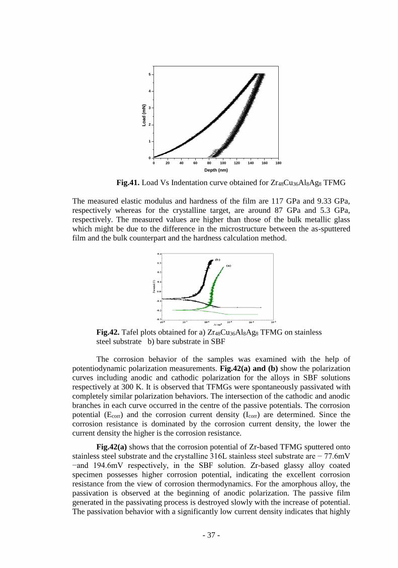
- 37 -
0 20 40 60 80 100 120 140 160 180
0
1
2
3
4
5
Lo
ad
(m
N)
Depth (nm)
Fig.41. Load Vs Indentation curve obtained for Zr48Cu36Al8Ag8 TFMG
The measured elastic modulus and hardness of the film are 117 GPa and 9.33 GPa,
respectively whereas for the crystalline target, are around 87 GPa and 5.3 GPa,
respectively. The measured values are higher than those of the bulk metallic glass
which might be due to the difference in the microstructure between the as-sputtered
film and the bulk counterpart and the hardness calculation method.
Fig.42. Tafel plots obtained for a) Zr48Cu36Al8Ag8 TFMG on stainless
steel substrate b) bare substrate in SBF
The corrosion behavior of the samples was examined with the help of
potentiodynamic polarization measurements. Fig.42(a) and (b) show the polarization
curves including anodic and cathodic polarization for the alloys in SBF solutions
respectively at 300 K. It is observed that TFMGs were spontaneously passivated with
completely similar polarization behaviors. The intersection of the cathodic and anodic
branches in each curve occurred in the centre of the passive potentials. The corrosion
potential (Ecorr) and the corrosion current density (Icorr) are determined. Since the
corrosion resistance is dominated by the corrosion current density, the lower the
current density the higher is the corrosion resistance.
Fig.42(a) shows that the corrosion potential of Zr-based TFMG sputtered onto
stainless steel substrate and the crystalline 316L stainless steel substrate are − 77.6mV
−and 194.6mV respectively, in the SBF solution. Zr-based glassy alloy coated
specimen possesses higher corrosion potential, indicating the excellent corrosion
resistance from the view of corrosion thermodynamics. For the amorphous alloy, the
passivation is observed at the beginning of anodic polarization. The passive film
generated in the passivating process is destroyed slowly with the increase of potential.
The passivation behavior with a significantly low current density indicates that highly

- 38 -
protective and uniform surface films have been formed on the surface of the TFMGs
exposed to the SBF solution. By contrast, there is no passivation in the procedure of
anodic polarization for the crystalline base metal alloy, and corrosion rate is found to
increase with the increase of potential. The structural and chemical homogenization is
thought to be responsible for the better corrosion resistance of the amorphous alloys
compared with the crystalline substrate in SBF solution. A porosity value of 0.067
was calculated using the relation for the Zr48Cu36Al8Ag8 TFMG on stainless steel
substrate indicating the good coverage of materials without imperfections in
corroboration to SEM analysis.
Electrochemical impedance spectra
Fig.43. AC impedance studies on Zr48Cu36Al8Ag8 TFMG on stainless steel
substrate and equivalent circuit (insert)
Fig.43. shows the electrochemical impedance spectra (EIS) of samples in SBF
solution. A lower polarization resistance value is observed for the crystalline 316L
stainless steel substrate compared to the Zr- based amorphous film coated specimen.
The Nyquist plots of the tested alloys present only one capacitive loop. The fitting
model can be represented by the equivalent circuit composed of one parallel
arrangement in series with the ohmic resistance and the result is shown Fig.43
(insert), where the CPE is constant phase element instead of pure capacitance, taking
account of the deviations of the system from the ideal state due to surface
heterogeneities; Rs is solution resistance; Rct is the electrochemical transfer
resistance. In general, observation of semi-circle in the Nyquist plot is very much
dependent on the resistance of the passive layer. According to our results, it is clearly
seen that the amorphous alloy coated specimen has larger polarization resistance
value than that of as sputtered glassy alloy specimen and the crystalline 316 L
stainless steel substrate, which is in accordance with the lower passive current density.
From the aforementioned analysis, the amorphous alloys present higher corrosion
resistance compared with the crystalline substrate in the SBF solution. The result from
electrochemical impedance spectra is consistent with that obtained by polarization
curves.
Cytotoxicity
Cytotoxicity test for the Zr48Cu36Al8Ag8 TFMG specimen and bare 316L
stainless steel substrate samples were assessed by MTT (3-[4, 5-dimethylthiazol-2-
yl]-2, 5-diphenyltetrazolium bromide) assay. Briefly 2×10⁴ cells/ml of HeLa cells
were directly seeded in 24 well plates containing samples coated on metal plates. It
was incubated for 24 hours at 37˚C in a humidified incubator supplied with 5% CO2.
After incubation, the growth medium was removed and the samples were washed
- 39 -
once with Phosphate buffer saline (PBS, pH 7.4). The metabolic activity was assessed
by incubating the samples with MTT solution (1mg/ml) at 37˚C for 3 hours. After
incubation, hundred microlitre of DMSO was added to dissolve the formazan crystals
(which gives purple colour if the cells are metabolically active). The absorbance was
measured at 540 nm using multi well plate reader (Spectra Max M3). The percentage
of viability was calculated by using the following formula
100x Control theof Absorbance
Test of AbsorbanceViability of %
An uncoated 316L stainless steel with 100 % viability was used as control. It was
found that the percentage of viability was 99.2 for Zr48Cu36Al8Ag8 sample which
indicates the non-cytotoxic nature of the sample.
Antimicrobial activity of sputtered nanocrystalline CuO immobilized fabrics
Structural analysis
The XRD spectra of sputtered copper oxide fabric of both woven and non-
woven kinds along with uncoated fabric were shown in Fig.44(a, b). The peaks
obtained on the uncoated fabric at 15.8, 23, 35 corresponds to woven type
(Fig.44c) and peaks at 17.9, 22.7 and 25 of non-woven type (Fig.44d) represent
the presence of cellulose in those fabrics. The peaks at 35.6 and 38.7 both belongs
to copper oxide (CuO) that was indexed to be (11-1) and (111) planes (JCPDS card
48-1548) respectively. The monoclinic crystal structure with average crystallite size
of 15nm was obtained.
Fig.44. XRD pattern of sputtered copper oxide on (a) woven (b) non-
woven fabrics; (c) uncoated woven fabrics (d) uncoated non woven
fabrics.
Antimicrobial studies
The activity against both gram negative and gram positive bacteria revealed
that copper oxide nanoparticles are dynamic antimicrobial agent by the measure of
zones in agar plates. The presence of bacterial colonies on the agar plate inoculated
with the test and control fabrics were shown in Fig.45 for E.coli and S.aureus.

- 40 -
Fig.45 Zone of inhibition produced by copper oxide nanocrystals
impregnated fabrics against E.coli bacteria (a) woven fabrics, (b)
non woven fabrics and S.aureus bacteria (c) woven fabrics, (d) non
woven fabrics
Clear transparent rings were obtained around the samples against the
background of agar medium, showing the killing effect of bacterial cells. At the same
time, the control fabric shows no symbol of inhibition against E.coli (Fig.45a, b) and
S.aureus (Fig.4c, d). The zone of inhibition for both woven and non-woven fabrics
give better results for E.coli and S.aureus are (15, 16mm) and (21, 20mm)
respectively.
Bacterial attachment on fabrics
Fig.46 FESEM image taken on woven fabrics (a) control (uncoated)
fabric with E.coli attachment (b) CuO Coated fabric (c) CuO coated fabric
showing E.coli cell wall shrinkage and (d) control (uncoated) fabric with
S.aureus attachment (e) CuO Coated fabric (f) CuO coated fabric showing
S.aureus cell wall shrinkage.
The morphology of the E.coli and S.aureus bacterial attachment and copper
oxide sputtered on woven and non-woven fabric was studied with the help of FESEM
as shown in Fig.46 and Fig.47. Cell wall damage of those bacteria was also noticed.
The rod shaped structure of the E.coli bacteria on woven and non woven fabrics was
confirmed as in Fig. (46a and 47a). The size of the bacteria was about 2-3µm. The
round shaped structure with an average size of about 2 µm of the S.aureus bacteria
was also confirmed as in Fig.(46d and 47d). The cotton fiber showed twisted ribbon
like structure with grooves, fibrils and the bacterial attachment was also found. The
presence of bacterial colonies was dense in the control fabric. Fig.(46b, 46e, 47b,
47e) represents the CuO coated onto the woven and non woven fabrics revealing the
uniform nature coating on the surface of the fiber.

- 41 -
Fig.47 FESEM image taken on non woven fabrics (a) control
(uncoated) fabric with E.coli attachment (b) CuO Coated fabric (c)
CuO coated fabric showing E.coli cell wall shrinkage and (d) control
(uncoated) fabric with S.aureus attachment (e) CuO Coated fabric (f)
CuO coated fabric showing S.aureus cell wall shrinkage.
Copper oxide nanocrystals which act as antimicrobial agent damages E.coli
bacteria by the effect of cell wall shrinkage and results in structural change from its
regular rod shape to irregular structure as shown in Fig. (46c and 46f). The circular
shaped S.aureus changes to irregular cubic structure as in Fig (47c and 47f) by the
effect of antimicrobial agent Copper oxide nanocrystals. Shallow hole like depression
also was seen on the bacterial cell.
The antimicrobial activity was further evaluated by measuring the killing
efficiency of bacteria (E.coli / S.aureus) against various time intervals. The copper
oxide sputtered test fabrics shows gradual increase in bacterial reduction efficiency
with respect to time interval. The total viable count of bacterial colonies decreases
progressively and reaches 100% within 10hours for S.aureus and 12 hours for E.coli
bacteria. In all these cases, both copper oxide sputtered woven and non-woven fabric
show better antimicrobial activity against both gram negative and gram positive
bacteria.
The antimicrobial activity against both gram positive and gram negative
bacterium showed good results for CuO sputtered fabric. The killing efficiency for
E.coli and S.aureus strains suggest that the sputtered CuO impregnated fabrics can be
used as promising antibacterial agents in medical applications.

- 42 -
Consultancy to Small Scale Inustry: Nano Markers, Trichy,
Tamilnadu
“Advice on Sputter Coating of Titanium Nitride onto Nickel or Chrome Plated
Stainless Steel Needles” to Nano Markers, Trichy –CNP 05/11
Date of Start : 02.12.2011 Date of Completion : 31.07.2012
Sputtering is the viable method over chemical methods like electroless
deposition and is a eco-friendly process which can be a good substitute for chemical
methods which cause severe environmental pollution problems. It is an advantageous
method for preparing adherent, uniform, thick and mirror reflection coatings for
multiple usage.
In this consultancy work, initially we did some feasibility studies on sputter
coating of Titanium Nitride on needles and blades made of stainless steel and mild
steel by optimizing the process parameters. After the satisfactory results, we have
advised Nano Marker’s Trichy to purchase DC Magnetron sputtering facility with the
complete required specifications. A DC magnetron sputtering equipment with a 4” dia
cathode assembly was purchased from VR Technologies, Bangalore and installed it at
Nano Marker’s Trichy. We performed few experiments in front of the client and
trained them. Thereafter, we have made few visits to their company and discussed
with them on the results of the experiments. They are advised to use the equipment for
doing other coatings such as Silver, Sn, Chromium, Copper and Brass. It is
understood from the discussion that they are able to fabricate successfully these
coatings now. The work has been completed to the satisfaction of the client. The
photographs of the facility created at their end with the products are shown under.
Photograph of Sputtering facility at Nano Markers, Photograph of Sputtering –Ar plasma,
Ar +N2 plasma
TiN coated needles TiN coated blades

- 43 -

- 44 -
ANNEXURE – II
Total Papers Published: 220 (International SCI Journals/Natioinal Journals/Cited
in SCOPUS)-188/23/9 Papers published in International SCI Journals/Natioinal Journals on various subject areas like: Electrochemical Science & Technology, Physical Sciences, Chemical
Science, and Nano Science & Technology.
List of Research Publications
Sl.
No.
Title of the Paper Authors Journal Name IF Citati
on
220. Antibacterial Activity
Studies of Ni and SnO2
loaded chitosan Beads
A.Ayesmariam
G.V.Sankaracharyulu,
M.Kashif,
S.Hussian,
M.Bououdina, and
M. Jayachandran
Materials Science
Forum 832(2015)
110-122
219. Enhanced Violet
Photomission of nano
crystline fluorine doped Zinc
oxide (FZO) thin filims
Anusha Muthukumar,
D.Arivuoli,
E.M.Manikandan,
M.Jayachandran
Optical Materials
47(2015)88-94
218 Synthesis, Structural and
Electrical Characterizations
of SnO2 Nanoparticles
N.Manjula, G.Selvan,
R.Perumalsamy, R.
Thirumamagal,
A.Ayeshamariam,
M. Jayachandran
International
Journal of
Nanoelectronsics
and Materials
8(2015),Accepted
217 Well aligned Graphene oxide
Nanosheets decorated with
Zinc Oxide Nanocrystals for
high Performance
Photocatalytic
Aapplication
K.Kaviyarasu,
C.Maria Magdalane,
E.Manikandan,
M.Jayachandran,
R.Ladchumananandasi
vam, S.Neellamani,
M.Maaza
International
Journal of
Nanoscience
14,
(2015)1550007(8
pages).
1.82
216 Studies on growth
mechanism of annealed
graphite powder and gas-
sensor application
P.Pounsuria,
Sahid hussian,
B.H.Abbas Sahul
Hameed,
R.Permalsamy,
R.Thirumamagal,
M.Jayachandran and
A.Ayeshamarimam
Materialls Science
Forum
832(2015)102-105
215
Structural,morphological and
optical characterization of
electroposited ZnSe thin
filims
A.Ayeshmariam,
M.kashif,
D.saravanakumar,
S.muthuraj
J.Indian Chem
Soc.,92(2015)
747754

- 45 -
M. Jayachandran M.Bououdina
214 Review on the materials
properties and
photoelectrochemical(Pec)
solar cells of CdSe,Cd1-X Znx
Se,Cd1-x Inx Se, thin films
S.Rani,
J.Shanthi,
S.Thangarajan
Ayeshamariam, and
M.Jayachandran
Material Science
Forum 832 (2015)
1-27
213 Biosynthesis of ZnO In2O3-
A.vera)Nanocomposites and
Antibacterial- al/Antifungal
Studies
A. Ayeshamariam, M.
Kashif, V.S Vidhya
,M.G.V.
Sankaracharyulu,
V.Swaminathan
M.Bououdia
M. Jayachandran
International
Journal of
Nanoelectronsics
and Materials
8(2015),Accepted
212 Properties of SnO2-Tio2
composite films deposited
using jet nebulizer Spary
Pyrolysis for gas sensor
N.Manjula,
G.Selvan,S.Thangaraj
an,,Ayeshamariam,S.
Muthuraja and
M. Jayachandran
Material Science
Forum 832(2015)
94-101
211 Studies on jet nebulizer
pyrolysed indium oxide thin
films and its
characterizations
S. Marikkannu, M.
Kashif, A.
Ayeshamariam, V. S.
Vidhya, N. Sethupathi,
Shakkthivel Piraman,
M. Jayachandran
International
Journal of
Nanoelectronics
and Materials
8(2015)99-110
210 Studies on the influence of
in and Zn doping on the
CdSe based photo electro
chemical(PEC) solar cells
using electron beam
evaporation technique
S.Rani,J.Shanthi,
S.Thangarajan,
Ayeshamariam, and
M.Jayachandran
Material Science
Forum 832(2015)
84-93
1.82
209 Multilayer and
Nanocomposite Hard
Coatings for Biomedical
Applications
M. Jayachandran Powder
Metallurgy &
Mining J. Powder
Metall Min 2014,
3:1
208. Bio-Synthesis of NiO and Ni
Nanoparticles and their
characterization
A.Ayeshamariam, M.
Kashif, S. Muthu raja,
S. Jagadeswari,
D. Saravanankumar,
N.M.I. Alhaji, A.
Uduman Mohideen,
M.Bououdina,
M. Jayachandran.
Digest Journal of
Nanomaterials and
Biostructures
9 (2014) 1007-
1019
207. Antimicrobial activity of
sputtered nanocrystalline
CuO impregnated fabrics.
B. Subramanian*, K.
Anu Priya,
S. Thanka Rajan,
.Dhandapani,
Materials Letters
128(2014) 1-4
2.367
1

- 46 -
M. Jayachandran.
206. 3D Hierarchically assembled
porous wrinkled paper-like
structure of ZnCo2O4 and
Co-ZnO@C as anode
materials for lithium-ion
batteries.
Giri Arnab, Pal
Provas, A. Ramadoss,
M. Jayachandran, Mahanty sourindra,
A. Panda.
Crystal Growth
and Design
14 (2014)3352-
3359
4.558
3
205. Studies of calcium-
precipitating oral bacterial
adhesion on TiN, TiO2
single layer, and TiN/TiO2
multilayer- coated 316L SS.
G. S.Kaliaraj,
A.Ramadass,
M.Sundaram,
B.subramanian,
M. Jayachandran.
J. Master. Sci
49 (2014) 7172-
7180
2.26
204.
Biosynthesis of ZnO-A.vera)
Nanocomposites and
Antibacteri-al/Antifungal
Studies
A. Ayeshamariam, M.
Kashif, V.S. Vidhya,
M.G. V.
Sankaracharyulu,
V. Swaminathan,
M. Bououdina,
M. Jayachandran
Journal of
Optoelectronics
and Biomedical
Materials
6(2014)85-99
2
203. Effect of Substrate
temperature on Indium Tin
Oxide (ITO) thin films
deposited by jet Nebulizer
Spray.
S.K Marikkannu,
Kashiff, Sethupathi,
V.S Vidya, A.P.
Sakthivel, M.
Bououdina,
M. Jayachandran
Materials Science
in Semiconductor
Processing 27
(2014) 562-568
3
202. Studies on jet nebulizer
pyrolysed indium oxide thin
flims
S.Marikannu,
M.Kasif,
A.Ayeshamariam,
N.Sethupathi, V.S.
Vidhya, S.Piraman,
M.Jayachandran
Journal of Ovonic
Research
10 (2014) 115-125
201. Optical Characterisation of
ZnSe Thin Flims by Using
Electro Deposition
Technique.
A.Ayeshamariam,
M. Kashif,
S. Muthu raja,
S. Jagadeswari,
D. Saravanankumar,
N.M.I. Alhaji,
A. Uduman Mohideen,
M.Bououdina,
M. Jayachandran
IJETAE 4, (2014)
584-590
200. Quantum confinement and
photoluminescence of well-
aligned CdO nanofibers by
solvothermal route
K. Kaviyarasu,
E. Manikandan,
J. Kennedy,
M. Jayachandran
Materials Letters
120(2014)243-245
2.28
199. Fabrication of nanowires of
Al-doped ZnO using
Thanka Rajan S.,
Subramanian B.,
J. Alloys and
Compounds,
2.13

- 47 -
nanoparticle assisted pulsed
laser deposition (NAPLD)
for device applications
Nandakumar A.K.,
Jayachandran M.,
Ramachandra Rao
M.S.
584(2014) 611-
616.
8
198. Preparation and
characterizations of SnO2
nanopowder and
spectroscopic (FT-IR, FT-
Raman, UV-Visible and
NMR) analysis using HF and
DFT calculations,
A.Ayeshamariam
A. Ramalingam S.
Bououdina
M. Jayachandran
Spectrochemica
Acta Part A:
Molecular and
Biomolecular
Spectroscopy,
118(2014)1135-
1143.
2.16
6
197. Morphological, structural,
and gas-sensing
characterization
of tin-doped indium oxide
nanoparticles
A. Ayeshamariam, M.
Kashif, M. Bououdina,
U. Hashim,
M. Jayachandran, M.E. Ali
Ceramics
International 40
(2014) 1321–1328
2.110
196. Organic Free Low
Temperature direct Synthesis
of Hierarchical Protonated
layered Titanates /anatase
TiO2 hollow spheres and
their task specific
applications
Narottam Sutradhar,
Sandip Kumar Pahari,
Muthirulandi
Jayachandran,
A Manuel stephan,
J.R.Nair,
Balasubramanian
Subramanian,
Hari.C.Bajaj, Haresh
M. Mody, Asit Baran
Panda
Journal of
Materials
Chemistry A1
(2013)
9122-9131.
6.101
195. Shape-selective synthesis of
non-micellar cobalt oxide
(CoO) nanomaterials by
microwave irradiations
Subrata Kundu,
M. Jayachandran
J. Nanopart Res
15(4) (2013) 1-13
3.287
11
194. Facile fabrication of dye-
sensitized solar cells utilizing
carbon nano tubes grown
over 2D hexagonal bimetallic
ordered mesoporous
materials
J. Balamurugan,
R. Thangamuthu,
A. Pandurangan,
M. Jayachandran
J.Power Sources
225 (2013) 364-
373
4.951
2
193. Formation of shape-selective
magnetic cobalt oxide
nanowires: environmental
application in catalysis
studies
Subrata Kundu,
M. D. Mukadam, S.
M. Yusuf,
M. Jayachandran
Crystal
Engineering
Communicatons
15 (2013) 482-497
3.842
10
192. CeO2 nanowires with high
aspect ratio and excellent
catalytic activity for selective
oxidation of styrene by
molecular oxygen
Provas Pal, Sandip
Kumar Pahari, Apurba
Sinhamahapatra,
Muthirulandi
Jayachandran, G.V.
Manohar Kiruthika,
Hari C. Bajaj, Asit
RSC Advances
3(2013) 10837-
10847.
2.56
5

- 48 -
Baran Panda
191. Fabrication of amorphous
Zr48Cu36Al8Ag8 thin films by
ion beam sputtering and their
corrosion behavior in SBF
for bio implants
B. Subramanian,
S. Yugeswaran,
Akira Kobayashi,
M. Jayachandran
Journal of Alloys
and Compounds
572(2013)163-169
2.13
5
190. Self-assembling of DNA-
Templated Au Nanoparticles
into Nanowires and their
enhanced SERS and
Catalytic Applications
S.Kundu,
M. Jayachandran
RSC Advancs
3 (2013)
16486-16498
2.56
14
189. Suitability evaluation of
plasma ion beam sputtered
TiN/TiOxNy multilayers on
steel for bio implants
B. Subramanian,
R. Ananthakumar,
S. Yugeswaran,
M. Jayachandran,
M. Takahashi,
Akira Kobayashi
Vacuum 88 (2013)
108-113
1.426
5
188. Nanoparticles of
In2O3/SnO2 (90/10) and
(80/20) at Two Different
Proportions and Its
Properties
Abbas Ayeshamariam,
Vinodh Sundar
Vidhya, Thangavel
Sivakumar,
Ramasamy
Mahendran,
Ramasamy
Perumalsamy,
Nallasamy
Sethupathy,
Muthurulandi
Jayachandran
Open Journal of
Metal, 3(2013)1-7
187. Green Synthesis of
Nanostructured Materials for
Antibacterial and Antifungal
activities
A. Ayeshamaraim
Tajun Meera Begum,
M.Jayachandran G.Praveen Kumar
M. Bououdina
Int. J. Bioassays
02 (01) (2013)
304-311
-
2
186. Compositional & surface
morphological analysis on
indium tin oxide thin films
prepared by radio frequency
sputtering
V. Malathy,
M. Jayachandran
Asian Journal of
Chemistry Vol.25,
Issue SUPPL,
(2013) S279-S282
185. Synthesis and
Characterizations of SnO2
Nanoparticles
A. Ayeshamariam,
V.S. Vidhya,
S. Sivaranjani, M.
Bououdina,
R. PerumalSamy,
M. Jayachandran
Journal of
Nanoelectronics
and Optoelectronic
8, (2013)273-280
184. Anodic corrosion behavior of
nanostructured TiN,
TiO2 single layer and
TiN/TiO2 multilayer coated
S.H.Gopi,R.Aanantha
kumar,B.Subramanian
, S Maruthamuthu,
M. Jayachandran
IEEE
Eplore,Advanced
Nanomaterials and
Emerging

- 49 -
316L SS
Engineering
Technologies
(ICANMEET),
(2013)331-334
183. Electrochemical Noise
analysis on Sputtered
Chromium Nitride Coated
D9 Steels
B.Subramanian,
K.Prabakaran,
V.V.Anusha Thampi
and
M. Jayachandran
Int. J.
Electrochem. Sci.,
8 (2013)12015-
12027
182. Size-controllable synthesis of
ITO nanoparticles and
application in gas sensor
A. Ayeshamariam,
R.Perumalsamy,
M. Jayachandran
Journal on
Photonics and
Spintronics
08/2013; 2(3):4.
181. Fabrication of Catalytically
active nanocrystalline
samarium (Sm)-doped
cerium oxide (CeO2) thin
films using electron beam
evaporation
Subrata Kundu,
Narottam Sutradhar,
R. Thangamuthu,
B. Subramanian,
Asit Baran Panda,
M. Jayachandran
J. Nanopart Res
14 (2012) 1040
3.287
6
180. Microstructural, Tribological
and Electrochem. Corrosion
Studies on Reactive DC
Magnetron Sputtered
Zirconium Nitride films with
Zr Interlayer on Steel
B. Subramanian,
V. Swaminathan
M. Jayachandran
Metals &
Materials
International
18 (2012)957-964
1.183
1
179. Influence of nitrogen flow
rates on the materials
properties of CrNx films
grown by reactive magnetron
sputtering
B. Subramanian
K. Prabakaran
M. Jayachandran
Bulletin of
Materials
Science35
(2012)505-511
0.88
5
178. Effect of substrate
temperature on structural,
morphological and optical
properties of crystalline
titanium dioxide films
prepared by DC reactive
magnetron sputtering
R. Ananthakumar
B. Subramanian
S. Yugeswaran
M. Jayachandran
Journal of
Materials Science:
Materials in
Electronics
23 (2012)
1898-1904
1.076
4
177. Deposition and
optoelectronic properties of
ITO (In2O3:Sn) thin films by
Jet Nebulizer Spray (JNS)
pyrolysis Technique
N. Sethupathi, P.
Thirunavukkarasu,
V.S. Vidhya, R.
Thangamuthu, G.V.M.
Kiruthika, K. Perumal,
Hari C. Bajaj and
M.Jayachandran
J.Materials
Science:Material
in Electronics
23 (2012)
1087 - 1093
1.076
5
176. Bio synthesis of calcium
hydroxyl apatite coating on
sputtered Ti/TiN nano
multilayers and their
corrosion behavior in
B.Subramanian,
P.Dhandapani,
S.Maruthamuthu and
M. Jayachandran
Journal of
Biomaterials
Applications 26
(2012) 687-705
2.246

- 50 -
simulated bodily solution
175. Surface modification of 316L
stainless steel with
magnetron sputtered TiN/VN
nanoscale multi layers for
bio implant applications
B.Subramanian,
R.Ananthakumar,
Akira Kobayashi and
M. Jayachandran
Journal of
Materials Science:
Materials in
Medicine 23
(2012) 329-338
1.076
11
174. Nanocomposite Ti-Si-N
coatings deposited by
reactive dc Magnetron
sputtering for biomedical
applications
B.Subramanian
R.Ananthakumar,
Akira Kobayashi and
M.Jayachandran
J.American.
Ceramic. Society
205 (2012) 5014-
5020
2.272
173. Electrochemical corrosion &
materials properties of
reactively sputtered
TiN/TiAlN multilayer
coatings
B. Subramanian,
R.Anandakumar,
Akira Kobayashi
M. Jayachandran
Ceramics
International 38
(2012) 477-485
1.751
16
172. Morphology and optical
measurements of
nanostructured In2O3: SnO2
nanoparticles
Ayeshamariam
C.Sanjeeviraja,
M.Jayachandran
M. Tajun Meera
Begam
World J. NanoSci.
Eng. 2 (2012) 6-12
1
171. A comparative study of
titanium nitride (TiN),
titanium oxy nitride (TiON)
and titanium aluminium
nitride (TiAlN), as surface
coatings for bio implants
B. Subramanian,
C.V. Muralidharan,
R.Ananda
kumar,
M. Jayachandran
Surface &
Coatings
Technology 205
(2011) 5014-5020
2.135
46
170. Effect of substrate
temperature on the properties
of reactively sputtered
TiN/NbN multilayers
B. Subramanian,
R.Ananthakumar,
M.Jayachandran
Crystal.Res.Tech
46 (2011) 1273-
1282
0.95
1
169. Preparation of chromium
oxynitride and chromium
nitride films by DC reactive
magnetron sputtering and
their material properties
B. Subramanian,
M. Jayachandran
Corros.Eng.Sci.
Technol 46 (2011)
554 – 561
0.50
168. Allylic and benzylic
oxidation over Cr (III) –
incorporated mesoporous
zirconium phosphate with
100% selectivity
A.Sinhamahapatra,
N.Sutradhar,
SK.Pahari, P.Pal,
HC.Bajaj,
M.Jayachandran A.B.Panda
Chem. Cat. Chem.
3 (2011) 1447-
1450
3.35
2
167. Study on (Mo/W) Se2
layered compound
semiconductors useful for
photoelectrochemical solar
cells
S.Mary Delphine,
M. Jayachandran C.Sanjeeviraja,
AW.Almusallam
Int.J.Chem. Tech.
Res.
3 (2011) 846-852
-
4
166. Facile Low-Temperature
Synthesis of Ceria and
.Sutradhar,
A.Sinhamahapatra, ,
Journal of Physical
Chemistry C

- 51 -
Samarium-Doped Ceria
Nanoparticles & Catalytic
Allylic Oxidation of
Cyclohexene
SK.Pahari,
M.Jayachandran B.Subramanian,
HC.Bajaj, A.B.Panda
115 (2011) 7628–
7637
4.52 26
165. Structural and
electrochemical impedance
spectro-scopic studies on
reactive magnetron sputtered
Ti oxynitride (TiON) thin
films
P. Padmavathy,
R. Ananthakumar,
B. Subramanian,
C. Ravidhas,
M. Jayachandran
Journal of Applied
Electrochemistry
41(2011) 751-756
1.49
4
164. Effect of nitrogen ion
implantation on structural
and microstructural
properties of reactive
magnetron sputtered TiN thin
films
B. Subramanian,
R.Ananthakumar,
N.Kobayashi,
M.Jayachandran
Transactions of the
Institute of Metal
Finishing
89 (2011) 28-32
1.62
1
163. Influence of RF power on the
growth mechanism,
preferential orientation and
optoelectronic properties of
nano crystalline ITO films
V.S. Vidhya, V.
Malathy,
T. Balasubramanian,
V. Saminathan,
C.Sanjeeviraja,
M. Jayachandran
Current Applied
Physics
11 (2011) 286-294
1.74
8
162. Structural and tribological
properties of DC reactive
magnetron sputtered titanium
/titanium nitride (Ti/TiN)
multilayered coatings
B. Subramanian,
R.Ananthakumar,
M. Jayachandran
Surface &
Coatings
Technology
205 (2011) 3485–
3492
2.135
20
161. Development of porous
silicon matrix and
characteristics of porous
silicon/ tin oxide structures
V.S.Vidya,
P.Padmavathy,
K.R.Murali,
C.Sanjeeviraja,
P.Manisankar,
M. Jayachandran
J.Non Crystalline
Solids
357(2011) 1522 -
1526
1.483
160. Photoluminescence studies
on porous silicon/ tin oxide
heterostructures
V.S.Vidya,
K.R.Murali,
B.Subramanian
P.Manisamkar,
C.Sanjeeviraja,
M. Jayachandran
J.Alloys and
Compounds
509(2011) 2842-
2845
2.13
1
159. Structural, optical, electrical
and luminescent properties of
electron beam evaporated
CdSe:In films
M.G.S.A.Basheer,K.S.
Rajni,
V.S.Vidya,
K.R.Murali,
M. Jayachandran
Crystal Research
and Technology
46(2011) 261- 266
0.95
12
158. Electrodeposition and
properties of nanocrystalline
ZnO films prepared in the
presence of anionic
surfactantSDS and ionic
V.S.Vidya, J.V.Rani,
A.R.Kumar
R.Thangamuth,
K.R.Murali,
M. Jayachandran
J.Materials
Science:Materials
in Electronics
22 (2011) 1460 -
65
0.93
3
- 52 -
liquid 1- butyl- 3
methylimidazolium methyl
sulfate
157. Photoluminescence studies
on ZnSe1-xTex films
K.Vijayakumar,
V.S.Vidya,
L.Amalraj,
K.R.Murali,
M. Jayachandran
J.Materials
Science:Materials
in
Electronics
22 (2011) 785 -
789
0.93
156. Structural, optical and
electrical properties of
ZnTe1-xSex thin films
V.S.Nagarathinam,
M.G.S.B.Ahamed
K.Vijayakumar,
L.Amalraj, A.R.Balu,
A.Thayumanavan
K.R.Murali,
M. Jayachandran
J.Materials
Science:Materials
in Electronics
22 (2011) 607 -
613
0.93
2
155. Characterization of Tin
disulphide thin films prepared
at different substrate
temperature using spray
pyrolysis technique
K. Vijayakumar,
C. Sanjeeviraja,
M. JayachandranL.
Amalraj
J. Mater Sci:
Mater Electronics
22 (2011) 929-935
0.93
3
154. Synthesization,
characterization and gas
sensing properties of SnO2
nanoparticles
A.Ayeshamariam,
C.Sanjeeviraja
M. Jayachandran
Int. J Chemical
and Analytical
Science
2 (2011) 54-61
-
1
153. Influence of substrate
temperature on the materials
properties of reactive DC
magnetron sputtered Ti/TiN
multilayered thin films
B.Subramanian,
R.Ananthakumar,
VS.Vidhya,
M. Jayachandran
Mat. Sci. and Eng.
B: Solid State
Materials for
Advanced
Technology
176 (2011) 1-7
1.715
19
152. Micro-structural and optical
properties of reactive
magnetron sputtered
Aluminum Nitride (AlN)
nano structured thin films
B. Subramanian,
V. Swaminathan,
M. Jayachandran
Current Applied
Physics
11 (2011) 43-49
1.90
7
151. Review of material
properties of (Mo/W)Se2-
layered compound
semiconductors useful for
photoelectrochemical solar
cells
S.M.Delphine,
M. Jayachandran C.Sanjeeviraja
Crystallography
Reviews
17 (2011) 281-301
4.091
7
150. Synthesis and
characterization of LiMVO4
cathode material produced by
sol-gel method
D. Prakash,
M. Jayachandran C.Sanjeeviraja
American Institute
of Physics
Conference
Proceedings(PAR
T A) 1349 (2011)
1.029

- 53 -
233-234
149. Nanomaterials preparations
by microwave-assisted
solution combustion method
and material properties of
SnO2 powder – A status
review
L.C. Nehru,V.
Swaminathan
M. Jayachandran C.Sanjeeviraja
Materials Science
Forum
671 (2011) 69-120
0.399
1
148. Review on gallium zinc
oxide films: Materials
Properties and preparation
techniques
S. Nagarani,
M. Jayachandran C.Sanjeeviraja
Materials Science
Forum
671(2011) 47-68
0.399
3
147. Influence of thickness on the
microstructural,
optoelectronic and
morphological properties of
nano crystalline ZnSe films.
M.G.S.A.Basheer,
V.S.Nagarathinam,
A.Thayumanvan,
K,R.Murali,
C.Sanjeeviraja,
M. Jayachandran
Materials Science
and Engineering B
171 (2010) 93-98
1.715
8
146. Effect of thickness on the
microstructural,
Optoelectronic,
morphological properties of
electron beam evaporated
ZnTe films
A.R.Balu,V.S.Nagarat
hinam,M.G.S.A.Bashe
er
A.Thayumanavan
K.R.Murali,
C.Sanjeeviraja,
M. Jayachandran
Journal of Alloys
and Compounds
502 (2010) 434–
438
2.135
10
145. Influence of substrate
temperature on the properties
of electron beam evaporated
ZnSe films
A.R.Balu,
V.S.Nagarathinam
A.Thayumanavan
K.R.Murali,C.Sanjeevi
raja,
M. Jayachandran
Cryst. Res.
Technol
45 (2010) 421 -
426
0.95
5
144. Structural, optical and
electrical properties of
electron beam evaporated
CdSe thin films
M.G.S.A.Basheer
V.S.Nagarathinam,
A.R.Balu, K,R.Murali,
A.Thayumanvan,C.Sa
njeeviraja,
M. Jayachandran
Cryst. Res.
Technol.
45 (2010) 387 -
392
0.95
8
143. Structural, optical, electrical
and morphological properties
of ZnTe films deposited by
electron beam evaporation
M.G.S.A.Basheer
V.S.Nagarathinam,
A.R.Balu,A.Thayuma
nvan, K,R.Murali,
C.Sanjeeviraja,
M. Jayachandran
J.Materials
Science:Materials
in Electronics
21 (2010)1229 -
1234
0.93
4
142. Thermal and optical
properties of Cd2SnO4 thin
films using photoacoustic
spectroscopy
K. Jeyadheepan,
Palanichamy,
V.Swaminathan,
M. Jayachandran, C.Sanjeeviraja
Appl Phys A: Mat.
Sci. and
Processing
98 (2010) 919
1.595
15
141. XRD and XPS
characterization of
A. Moses Ezhil Raj, S.
Grace Victoria, V.
Applied Surface
Science
1.616

- 54 -
mixed valence Mn3O4
hausmannite thin films
prepared by chemical
spray pyrolysis technique
Bena Jothy,
C. Ravidhas, Joachim
Wollschlaer,
M. Suendorf,
M. Neumann,
M. Jayachandran,
C.Sanjeeviraja
256 (2010) 2920–
2926
59
140. Thickness Dependence of
Structural, Electrical &
Optical Properties of
Sputter Deposited Indium
Tin Oxide Films
S. Sivaranjani, V.
Malathy, Prince, B.
Subramanian,
T. Balasubramanian,
C. anjeeviraja,
M,Jayachandran,
V.Swaminathan
Advanced Science
Letters
3 (2010) 434–441
1.253
2
139. Structural and electrical
studies of nano structured
Sn1-x SbxO2 (x = 0.0, 1,
2.5, 4.5 and 7 at%)
prepared by co-
precipitation method
V. Senthilkumar, P.
Vickraman,
C. Sanjeeviraja,
M. Jayachandran
J. Mater Sci:
Mater Electron
21 (2010) 343–348
0.93
17
138. Defect engineering and
opto electronic property
modifications by 1.5
MeV Li+ implantation on
nano crystalline MgIn2O4
thin films
A. Moses Ezhil Raj,
T. Som,
C. Sanjeeviraja,
M. Jayachandran
Radiation Effects
& Defects in
Solids:
Incorporating
Plasma Sci. &
Plasma Tech.
165 (2010) 265–
276
0.55
2
137. Structural and optical
properties of indium tin
oxide (ITO) thin films
with different
compositions prepared by
electron beam
evaporation
V. Senthilkumar, P.
Vickraman,
M. Jayachandran,
C. Sanjeeviraja,
Vacuum
84 (2010) 864–869
0.975
35
136. Spray deposition and
property analysis of
anatase phase titania
(TiO2) nanostructures
A. Moses Ezhil Raj,
V.Agnes, V. Bena
Jothy, C. Ravidhas,
Joachim Wollschlaer,
M. Suendorf,
M. Neumann,
M. Jayachandran,
C.Sanjeeviraja
Thin Solid Films
519 (2010) 129–
135
1.727
11
135. Growth of ZnSe thin
layers on different
substrates and their
structural connsequences
with bath temperature
A. Moses Ezhil Raj, S.
Mary Delphine, C.
Sanjeeviraja,
M. Jayachandran
Physica B:
Condensed Matter
405 (2010) 2485-
2491
1.056
18
134. Role of substrate V. Malathy, S. J Mater Sci: Mater

- 55 -
temperature on the
structural, optoelectronic
and morphological
properties of (400)
oriented indium tin oxide
thin films deposited using
RF sputtering technique
Sivaranjani, V. S.
Vidhya,
T. Balasubramanian,
Joseph Prince,
C. Sanjeeviraja,
M. Jayachandran
Electron.
21 (2010) 1299–
1307
0.93
5
133. Microstructura, mechanical
and electrochemical
corrosion properties of
sputtered Titanium –Al-
Nitride films for bio implants
B. Subramanian,
R.Ananthakumar,
M. Jayachandran
Vacuum
85 (2010) 601-609
1.431
13
132. Synthesis and
characterization of SnO2
nanopowder prepared by
precipitation method
V.Senthil kumar,
P.Vickraman,
M. Jayachandran,
C.Sanjeeviraja
Journal of
Dispersion Science
and Technology
31 (2010) 1178-
1181
0.628
3
131. Effects of deposition
temperature on materials
properties of magnetron
sputtered titanium nitride
coatings on mild steel
substrates with Ni
interlayer
B. Subramanian ,
K.Ashok,G.Selvan,
V.S.Kumar,
M. Jayachandran
Surface
Engineering
26 (2010) 555-561
0.432
7
130. Preparation of anatase TiO2
thin films for dye-sensitized
solar cells by DC reactive
magnetron sputtering
technique
V.Senthil kumar,
M. Jayachandran,
C.Sanjeeviraja
Thin Solid Films
519 (2010) 991-
994
1.727
18
129. Effects of annealing
temperature on structural,
optical, and electrical
properties of antimony-
doped Tin oxide thin
films
V.Senthil kumar,
P.Vickraman,
JJ.Prince,
M. Jayachandran,
C. Sanjeeviraja
Philosophical
Magazine Letters
90 (2010) 337-347
1.262
14
128. Fabrication techniques and
materials properties of
dielectric MgO thin films- A
status review
A.M.E Raj
M. Jayachandran,
C. Sanjeeviraja
CIRP Journal of
Manuf. Sci.
Technol.
2 (2010) 92-113
14
127. Structural, optoelectronic and
electrochemical properties of
nickel oxide films
B.Subramanian,
Mohammed Ibrahim,
K.R.Murali,
V.S.Vidya,
C.Sanjeeviraja,
M. Jayachandran
J.Materials
Science:Materials
in Electronics
20 (2009) 953-957
0.93
9
126. Crystal Structure and thermal
characterization of Cadmium
oxalate [CdC2O4.3H2O] and
A. Moses Ezhil Raj,
D.Deva Jayanthi,
V.Bena Jothy,
Inorganica
Chimical Acta

- 56 -
barium doped cadmium
oxalate
[Ba0.5Cd0.5(C2O4).5H2O]
single crystals grown in silica
gel
M. Jayachandran,
C.Sanjeeviraja
362 (2009) 1535-
1540
1.899 6
125. Optimized deposition and
characterization of
nanocrystalline Mg-In Oxide
thin films for Opto-electronic
applications
A. Moses Ezhil Raj,
C.Ravidhas,
R.Ravishankar,
A.Rathish Kumar, G.
Selvan,
M. Jayachandran,
C.Sanjeeviraja
Materials Research
Bulletin
44 (2009) 1051-
1057
0.944
5
124. Effect of Substrate
Temperature on structural
and material properties of
Zirconium nitride films on
D9 steel substrates
K.Ashok,
B.Subramanian,
P.Kuppusamy,
M. Jayachandran
Cryst. Res.
Technol.
44 (2009) 511-516
0.95
9
123. Polyvinylidenefluoride
(PVdF) based novel polymer
electrolytes complexed with
Mg(ClO4)2
P.Vickraman,
V.Aravindan,
T.Srinivasan,
M. Jayachandran
Eur. Phys. J. Appl
Phys
45 (2009) 11101
(pp.1-5)
0.899
1
122. Evaluation of Corrosion and
wear resistance Titanium
Nitride coated on mild steel
(MS) with brush plated
nickel interlayer
B.Subramanian,
K.Ashok,
K.Subramanian,
D.Sastikumar,
M. Jayachandran
Surface
Engineering
25 (2009) 890-895
0.633
10
121. Molybdenum oxide (MoO3)
thin films based
electrochromic cell
characterization in 0.1 M
LiClO4.PC electrolyte
R.Sivakumar,
K.Shanthakumari,
A.Thayumanavan
M. Jayachandran,
C..Sanjeeviraja
Surface
Engineering
25 (2009) 548-554
0.633
120. Ultrasonic study on binary
mixture containing dimethyl
formamide and methanol
over the entire miscibility
range (0<x<1) at
temperatures 303-323
A. Moses Ezhil Raj,
L.B.Reshmi,
V.Bena Jothy,
M. Jayachandran,
C.Sanjeeviraja
Fluid Phase
Equlibria
281 (2009) 78-86
17
119. Amorphous to crystalline
transition and optoelectronic
properties of nanocrystalline
ITO films sputtered with high
RF power at room
temperature
V. Malathy, S.
Sivaranjani,
VS.Vidhya,
J. Joseph Prince,
T. Balasubramanian,
C. Sanjeeviraja ,
M. Jayachandran
J. Non Cryst.
Solids
355 (2009) 1508-
1516
1.252
17
118. Effect of embedded lithium A. Moses Ezhil Raj, Radiation Physics

- 57 -
nanoclusters on structural,
optical and electrical
characteristics of MgO thin
films
V. Bena Jothy, C.
Ravidhas, T. Som,
M. Jayachandran,
C.Sanjeeviraja
and Chemistry
78 (2009) 914-921
1.149 5
117. Materials properties of
electrodeposited NiFe and
NiCoFe coatings
B.Subramanian,
K.Govindan,
V.Swaminathan,
M. Jayachandran
Trans. of the Inst.
of Metal Finishing
87 (2009) 325-
1.62
2
116. Magnesium Indium Oxide
(MgIn2O4)spinel thin films:
chemical spray pyrolysis
(CSP) growth and materials
characterizations
A. Moses Ezhil Raj,
G. Selvan,
M. Jayachandran,
C.Sanjeeviraja
J. of Colloid and
Interface Science
328 (2008) 396-
401
3.019
5
115. Effect of substrate
temperature on the structural
properties of magnetron
sputtered titanium nitride
thin films with brush plated
nickel interlayer on MS
B. Subramanian,
K.Ashok,
M. Jayachandran
Applied Surface
Science
255 (2008) 2133-
2138
1.616
21
114. The influence of substrate
temperature on the electrical
properties of ZnO films
prepared by the RF
magnetron sputtering
technique
K.Saravanakumar,
V.Senthilkumar,
M. Jayachandran,
C.Sanjeeviraja,
V.Ganesan, Raushan
B. Kaizhaiganova,
T.Vasudevan,
M.S.Lee
Nano: Brief
Reports and
Reviews
3 (2008) 469-476
1
113. Studies on transparent spinel
magnesium indium oxide
thin films prepared by
chemical spray pyrolysis
A. Moses Ezhil Raj,
V.Senthikumar,
V.Swaminathan,
Joachim Wollschlager,
M.Suendorf,
.Neumann,
M. Jayachandran,
C.Sanjeeviraja
Thin Solid Films
517 (2008) 510-
516
1.727
11
112. Synthesis and
characterization of spray
pyrolysed MgIn2O4 spinel
thin films for novel
applications
A.Moses Ezhil raj,
B.Subramanian,
V.Senthil kumar,
M. Jayachandran,
C.Sanjeeviraja
Physica E: Low
Dimen. Systems
and Nano
structures
40 (2008) 467 –
473
1.177 1
111. High temperature grown
transition metal oxide thin
films tuning physical
properties by MeV N+ -ion
bombardment
R.Sivakumar,
C.Saneeviraja,
M. Jayachandran R.Gopalakrishnan,
S.N.Sarangi,
D.Paramanik, T.Som
J.Phys.D:Appl.Phy
s.
41 (2008) art.
No.125304 467 -
473
2.083
5
110. Growth mechanism and
optoelectronic properties of
A.Moses ezhil raj,
K.C.Lalithambika,
Physica B:
Condensed Matter.

- 58 -
nanocrystalline In2O3 films
prepared by chemical spray
pyrolysis of metal-organic
precursor
V.S.Vidhya,
G.Rajagopal,
A.Thayumanavan
M. Jayachandran,
C.Sanjeeviraja
403 (2008) 544-
554
1.056 42
109. Influence of metal organic
and inorganic precursors on
spray pyrolyzed ceramic
MgO (200) thin films for
epitaxial over layers
A.Moses Ezhil Raj,
K.Vijayalakshmi,
G.Selvan,
M. Jayachandran,
C.Sanjeeviraja
J. Non Cryst.
Solids
354 (2008) 3773 –
3779
1.252
4
108. Growth aspects of barium
oxalate monohydrate single
crystals in gel medium
A.MosesEzhil raj,
D.Deva
Jayanthi,V.Bena
Jothy,
M. Jayachandran,
C.Sanjeeviraja
Cryst. Res.
Technol.
43 (2008) 1307 –
1313
0.896
3
107. Characterization of reactive
DC magnetron sputtered
TiAlN thin films
B.Subramanian,
K.Ashok,
P.Kuppusamy,
C.Sanjeeviraja,
M. Jayachandran
Cryst. Res.
Technol.
43 (2008) 1078 –
1082
0.896
7
106. Reactive DC Magnetron
Sputtered Zirconium Nitride
(ZrN) thin film and its
characterization
B.Subramanian,
K.Ashok,
P.Kuppusamy,
C.Sanjeeviraja,
M. Jayachandran
J. of Physics:
Conference Series
114 (2008) 012039
(9 pp)
2
105. Materials properties of
nanostructured titanium
nitride thin films synthesized
by DC reactive magnetron
sputtering
B.Subramanian,
M. Jayachandran
Trans. Insti. Metal
Finishing
86 (2008) 62 - 65
1.736
104. Structure, Mechanical and
Corrosion properties of DC
reactive magnetron sputtered
Aluminium Nitride (AlN)
hard coatings on mild steel
substrates
B. Subramanian,
K.Ashok,
M. Jayachandran
J.Applied
Electrochemistry
38 (2008) 619 –
625
1.697
2
103. Electrochemical corrosion
behavior of magnetron
sputtered TiN coated steel in
simulated bodily fluid and its
hemocompatibility
B. Subramanian,
M. Jayachandran
Materials Letters
62 (2008) 1727 –
1730
1.94
13
102. Optoelectronic and
electrochemical properties of
NiO films deposited by DC
magnetron sputtering
technique
B.Subramanian,
M.Mohamed Ibrahim,
V.Senthil
Kumar,K.R.Murali,
C.Sanjeeviraja,
M. Jayachandran
Physica.B:
Condensed Matter.
402 (2008) 4104 -
4110
1.056
48
101. Properties of ZnSe films K.R.Murali, Ionics 14 (2008) 0.899

- 59 -
pulse electrodeposited in the
presence of phosphotungstic
acid
V.S.Vidya,
M. Jayachandran
569 – 575
100. Synthesis and
characterization of copper
substituted lithium
manganate spinels
K.R.Murali,
T.Saravanan,
M. Jayachandran
J.Materials
Science:Materials
in Electronics
19 (2008) 533 –
537
0.93
8
99. Tailoring optical and
electrical properties of MgO
thin films by 1.5 MeV H+
implantation to fluences
A.Moses Ezhil Raj,
T.Som, V.Ganesan,
M. Jayachandran,
G.Selvan,
V.Swaminathan,
C.Sanjeeviraja
Nucl. Instr and
Methods in Phys.
Research B
266 (2008) 2564 -
2571
1.156
9
98. Effect of phosphotungstic
acid on the properties of
pulse electrodeposited ZnSe
films
K.R.Murali,
V.S.Vidya,
M. Jayachandran
Mat. Sci. Semi.
Proc.10 (2007)
155 - 158
0.388
2
97. Structural and optical
properties of electron beam
evaporated CdSe thin
J.Suthan
Kissinger,
M.Jayachandra,
K.Perumal,
C.Sanjeeviraja
Bull.Mater.Sci
30 (2007) 547-551
0.51
60
96. Spray pyrolysis deposition
and characterization of
highly (100) oriented
magnesium oxide thin films
A.Moses Ezhil Raj,
L.C.Nehru,
M. Jayachandran,
C.Sanjeeviraja
Cryst. Res.
Technol.
42 (2007) 867-875
0.896
46
95. Coloration and bleaching
mechanism of tungsten oxide
thin films in different
electrolytes
R.Sivakumar,
K.Shanthakumari,
A.Thayumanavan,
M. Jayachandran,
C.Sanjeeviraja
Surf.Engg.
23 (2007) 373-379
0.432
3
94. Synthesis and materials
properties of transparent
conducting In2O3 films
prepared by sol-gel-spin
coating technique
E.Savarimuthu,
K.C.Lalithambika,
A.Moses Ezhil Raj,
L.C.Nehru,
S.Ramamurthy,
A.Thayumanavan,
M. Jayachandran,
C.Sanjeeviraja
J.Phys.Chem.
Solids
68 (2007) 1380-
1389
1.189
25
93. Optoelectronic properties of
nano crystalline F-doped
SnO2 (FTO) films prepared
by sol-gel spin technique
N.Sankarasubramania
n, K.Shanthakumari,
V.S.Vidhya,
L.C.Nehru,
B.Subramanian,
A.Thayumanavan,
S.Ramamurthy,
C.Sanjeeviraja,
M. Jayachandran
Optoelectronics
and advanced
materials Rapid
communications
1 (2007) 417-424
0.451
1

- 60 -
92. Characterization of reactive
magnetron sputtered
nanocrystalline Titanium
Nitride (TiN) thin films with
Brush plated Ni interlayer
B. Subramanian,
M. Jayachandran
J.Applied
Electrochemistry
37 (2007) 1069-
1075
1.697
16
91. Properties and corrosion
behavior of reactive
magnetron sputtered TiAlN
coatings on AISI 316 LSS in
simulated bodily fluid
B. Subramanian,
G.Umamaheswari
M. Jayachandran
Corrosion
Engg.Sci & Tech.
42 (2007) 349-355
0.632
4
90. Structural and
electrochemical
characterization of Ni
nanostructure films on steels
with brush plating and
sputter deposition
B.Subramanian,
S.Mohan, Sobha
Jayakrishnan,
M. Jayachandran
Current Applied
Physics
7 (2007) 305-313
1.586
16
89. Photoacoustic studies on
optical and thermal
properties of p-type and n
type nanostructured porous
silicon for (100) and (111)
orientations
R.Srinivasan,
M. Jayachandran
Ramachandran
Cryst. Res.
Technol.
42 (2007) 266-274
0.896
15
88. MeV N+-ion irradiation
effects on α-MoO3 thin films
R.Sivakumar,
C.Sanjeeviraja,
M. Jayachandran R.Gopalakrishnan,
S.N.Sarangi,
D.Paramanik, T.Som
J. Appl. Physics
101 (2007)
034913-(1-5)
2.072
16
87. Modification of WO3 thin
films by MeV N+-ion beam
irradiation
R.Sivakumar,
C.Sanjeeviraja,
M. Jayachandran,
R.Gopalakrishnan,
S.N.Sarangi,
D.Paramanik, T.Som
J.Phys.Condense
Matter
19 (2007) 186204
(9pp)
0.964
12
86. Characterization on electron
beam evaporated α-MoO3
thin films by the influence of
substrate temperature
R.Sivakumar,
R.Gopalakrishnan,
M. Jayachandran C.Sanjeeviraja
Current Applied
Physics
7 (2007) 51 - 59
1.586
36
85. An Electrochromic device
(ECD) cell characterization
on electron beam evaporated
MoO3 films by intercalating/
deintercalating the H+ ions
R.Sivakumar,
C.S.Gopinath,
M. Jayachandran,
C.Sanjeeviraja,
Current Applied
Physics
7 (2007) 76 – 86
1.586
25
84. Preparation and
characterization of electron
beam evaporated WO3 thin
films
R.Sivakumar,
R.Gopalakrishnan
M. Jayachandran,
Optical Materials
29 (2007) 679-687
1.728
62
83. Biodiesel production from
vegetable oils by alkali
D. Jayaperumal,
S.T.Selvamani,
Bull.
Electrochemistry
-

- 61 -
catalyzed methanolysis
method
T. Selvaganapathy ,A.
Madhava Mayandi,
M. Jayachandran
23 (2007) 231-236
82. Production of biodiesel from
different vegetable oils by
alkali catalyzed
transesterification
D. Jayaperumal,
S.T.selvamani,
T.Selvaganapathy, A.
Madhava Mayandi,
M. Jayachandran
Bull.
Electrochemistry
23 (2007) 217-222
81. Development of a novel high
optical quality ZnO thin
films by PLD for III–V opto-
electronic devices
K.Ramamoorthy,
C.Sanjeeviraja,
M. Jayachandran,
K.Sankaranarayanan,
Pankaj Misra,
L.M. Kukreja
Current Applied
Physics
6 (2006) 103-108
1.586
63
80. Preparation and
characterization of
nanostructured Tin oxide
(SnO2) films by sol-gel spin
coating technique
E.Savarimuthu,
N.Sankarasubramania
n, B.Subramanian,
M. Jayachandran,
C.Sanjeeviraja,
S.Ramamoorthi
Surface
Engineering
22 (2006) 268-276
0.432
8
79. Surface characterization
studies of nickel-chromium
PVD:EB evaporated on low
carbon steel samples
B.Subramanian,
M. Jayachandran S.Jayakrishnan
Surface
Engineering
22 (2006) 447-451
0.432
2
78. Investigation on the X-Ray
Photoelectron Spectroscopic
(XPS), cyclic voltammetric
analyses of WO3 films and
their electrochromic response
in FTO/EC/ Electrolyte/FTO
cells
R.Sivakumar,
M. Jayachandran, V.
Vijayan,
C. Sanjeeviraja
Smart Materials
and Structures
15 (2006) 877-888
0.432
33
77. Intercalation studies on
electron beam evaporated
MoO3
films for
electrochemical devices
R.Sivakumar,
P.Manisankar
M. Jayachandran,
C..Sanjeeviraja
Solar Energy Mat.
and Solar Cells 90
(2006) 2438-2448
3.858
21
76. Particle size analysis of
Barium Titanate powder by
slow-rate sol-gel process
route
R. Balachandran,
H.K. Yow,
M. Jayachandran ,
W.Y.W. Yusof,
V. Saaminathan
IEEE IntL. Conf.
on Semi conductor
Elec., proc., ICSE,
art. No. 4266641,
(2006) 406-409
1
75. Characterization of WO3
films prepared at different
deposition currents on CTO
substrates
R.Vijayalakshmi,
M. Jayachandran C.Sanjeeviraja
Synthesis &
Reactivity in
Inorg.,Metal Org.
& Nanometal
chem..
36 (2006) 89-94
0.569
4
74. Sequential deposition of Cu-
Ni by Electron beam
evaporation and its
B.Subramanian,
M. Jayachandran Sobha Jayakrishnan
Transaction of the
Institute of Metal
Finishing
1.376

- 62 -
characterization 84 (2006) 52–55
73. Pulsed electrodeposition and
characterization of
molybdenum diselenide thin
film
S.Mary Delphine,
M. Jayachandran C.Sanjeeviraja
Mater. Res. Bull
40 (2005) 135-147
22
72. Particle induced X-ray
emission spectroscopic
(PIXE) and surface
morphological (AFM)
studies on electron beam
evaporated WO3 films
R.Sivakumar,
V.Ganesan
V.Vijayan
M. Jayachandran C.Sanjeeviraja
Surface
Engineering
21 (2005) 315-319
1.879
2
71. A novel nano-architecture for
ZnO thin films on <100> Si,
GaAs and InP single crystal
wafers by L-MBE as value in
nano-robotic(machining)
device fabrication efforts
K.Ramamoorthy,
C.Sanjeeviraja
M. Jayachandran K.Sankaranarayanan
V. Ganesan, Pankaj
Misra
L.M. Kukreja
Materials Science
in Semiconductor
Processing
8 (2005) 555 - 563
0.388
9
70. Electron beam evaporated
Mo Oxide Films: a study of
elemental and surface
morphological properties
R. Sivakumar, V.
Vijayan, V.Ganesan
M. Jayachandran C.Sanjeeviraja
Smart Materials
and Structures
14 (2005) 1204-
1209
0.432
11
69. Studies on nickel
electrodeposits on dc
magnetron sputtered copper
substrates
B.Subramanian,
S.Jayakumar
M. Jayachandran Sobha Jayakrishnan
Surface
Engineering
21 (2005) 151-155
0.432
1
68. Characterization of Brush
plated Sn and SnSe
B.Subramanian,
S.Jayakumar
M. Jayachandran S.Mohan, Sobha
Jayakrishnan
Indian Surface
Finishing
2 (2005) 64-68
67. Review on WO3 thin films:
Materials properties,
preparation techniques and
electrochromic devices
M. Jayachandran, R.
Vijayalakshmi,
Visalakshi Ravindran,
C.Sanjeeviraja
Transactions of the
SAEST
40 (2005) 42-61
2
66. Development of a novel high
speed (electron-mobility)
epi-ZnO thin films by L-
MBE for III-V opto-
electronic devices
K.Ramamoorthy,
M. Jayachandran K.Sankaranarayanan ,
Pankaj Misra,
L M Kukreja,
C.Sanjeeviraja
Current Applied
Physics
4 (2004) 679-684
1.74
9
65. Epitaxial lattice matching
between epi-n-IZO thin films
and <100> Si, GaAs and InP
wafers with out any buffer
layers by L-MBE technique a
novel development for III-V
opto - electronic devices
K.Ramamoorthy,
C.Sanjeeviraja
M. Jayachandran K.Sankaranarayanan ,
Pankaj Misra
L M Kukreja,
Materials
Chemistry and
Physics
84 (2004) 14 – 19
10

- 63 -
64. Fabrication of novel nano-
architecture for IZO thin
flims on <100> Si, GaAs and
InP single crystal wafers by
L-MBE
K.Ramamoorthy,
C.Sanjeeviraja
M. Jayachandran K.Sankaranarayanan ,
Pankaj Misra,L M
Kukreja,
Surface
Engineering
20 (2004) 205-210
0.633
1
63. Preparation and
characterization of spray
deposited n-type WO3 thin
films for electrochromic
devices
R.Sivakumar,A.Moses
Ezhil Raj,
B.Subramanian,
M. Jayachandran D.C.Trivedi,
C.Sanjeeviraja
Materials Research
Bulletin
39 (2004) 1479-89
71
62. Effect of annealing on
structural surface and optical
properties of - MoO3 thin
films by PVD:EBE for
electrochromic devices
R.Sivakumar,
M. Jayachandran C.Sanjeeviraja
Surface
Engineering
20 (2004) 385-390
0.633
8
61. Study of the potassium ion
insertion of the
electrodeposited
electrochromic tungsten
trioxide thin films
R.Vijayalakshmi,
M. Jayachandran,
D.C.Trivedi,
C.Sanjeeviraja
Ionics
10 (2004) 151-154
6
60. Studies on the effect of
substrate temperature on (VI-
VI) textured tungsten oxide
(WO3) thin films on glass,
SnO2:F substrates by
PVD:EBE technique for
electrochomic devices
R.Sivakumar
M. Jayachandran C.Sanjeeviraja
Materials
Chemistry and
Physics
87 (2004) 439-445
31
59. Epi-n-IZO thin films/<100>
Si, GaAs and InP by L-MBE
– a novel feasibility study
for SIS type Solar cells
K.Ramamoorthy,
C.Sanjeeviraja
M. Jayachandran K.Sankaranarayanan ,
Pankaj Misra,.L M.
Kukreja,
Solar Energy
77 (2004) 193-201
9
58. SrAl4O7:Eu2+ nanocrystals:
synthesis and fluorescence
properties
K.R.Sophya Preethi,
Chung-Hsin Lu,
J.Thirumalai, R
Jagannathan, T S
Natarajan N.Nayak,
I Radhakrishna,
M. Jayachandran,
D C Trivedi
J. Phys. D: Appl.
Phys
37 (2004) 2664-
2669
15
57. Preparation and
characterization of tin
diselenide thin film by spray
pyrolysis technique
L.Amalraj
M. Jayachandran C.Sanjeeviraja
Materials Research
Bulletin
39 (2004) 2193-
2201
19
56. A study of sequentially
evaporated Nickel
B.Subramanian,
M. Jayachandran,
Electrochemical
Society of India 53

- 64 -
Aluminum coatings Sobha Jayakrishnan (2004) 75
55. Photoelectrochemical
characteristics of brush
plated tin sulfide thin films
B.Subramanian,
M. Jayachandran,
C.Sanjeeviraja
Solar Energy
Materials and
Solar Cells 79
(2003) 57-65
38
54. Epi-n-ZnO/<100> Si, GaAs
and InP by L-MBE: a novel
approach for III– V devices
K.Ramamoorthy,
C.Sanjeeviraja
M. Jayachandran K.Sankaranarayanan ,
Pankaj Misra
L M Kukreja,
Materials Sci. in
Semiconductor
Processing 6
(2003) 219-224
14
53. Pulsed electrodeposition and
characterisation of tungsten
diselenide thin films
S.Mary Delphine,
M. Jayachandran C.Sanjeeviraja
Materials
Chemistry and
Physics 81 (2003)
78-83
28
52. Materials properties of
electrodeposited SnS0.5Se0.5
films and characterization of
photoelectrochemical solar
cells
B.Subramanian,
M. Jayachandran,
C.Sanjeeviraja
Materials Research
Bulletin 38 (2003)
899-908
13
51. Structural, electrochromic
and FT-IR studies on
electrodeposited tungsten
trioxide films
R.Vijayalakshmi,
M. Jayachandran,
C.Sanjeeviraja
Current Applied
Physics 3 (2003)
171-175
41
50. Influence of alloying
additives on the performance
of commercial grade
aluminium as galvanic anode
in alkaline zincate solution
for use in primary alkaline
batteries
M.Paramasivam,
M. Jayachandran,
S.Venkatakrishna Iyer
Journal of Applied
Electrochemistry
33 (2003) 303-309
25
49. Electrosynthesis and
characterisation of n-WSe2
thin films
J.Jebaraj Devadasan,
C.Sanjeeviraja
M. Jayachandran
Materials
Chemistry and
Physics 77 (2003)
397-401
21
48. Spray pyrolysis growth and
material properties of In2O3
films
J.Joseph Prince,
S.Ramamurthy
B.Subramanian,
C.Sanjeeviraja
M. Jayachandran
Journal of Crystal
Growth
240 (2002) 142-
151
88
47. Spray pyrolysised tin
disulphide thin film and
characterization
L.Amalraj,
C.Sanjeeviraja,
M. Jayachandran
Journal of Crystal
Growth
234 (2002) 683-
689
35
46. Brush plating of tin(II)
selenide thin films
B.Subramanian,
M. Jayachandran,
C.Sanjeeviraja
Journal of Crystal
Growth
234 (2002) 421-
426
75
45. Review on materials B.Subramanian, Bull.

- 65 -
properties of Sn(S, Se)
compound semiconductors
useful for
photoelectrochemical solar
cells
C.Sanjeeviraja,
M. Jayachandran
Electrochemistry
18 (2002) 349-366
10
44. Ce3+ doped stillwellites: a
new luminescence system
with strong ion lattice
coupling
L.C.Nehru,
K.Marimuthu,
M. Jayachandran,
Chung-Hsin Lu,
R.Jagannathan
J. Physics D:
Applied Physics
34 (2001) 2599-
2605
17
43. Cathodic electrodeposition
and analysis of SnS films for
photoelectrochemical cells
B.Subramanian,
C.Sanjeeviraja,
M. Jayachandran
Mat. Chem. and
Phys.
71 (2001) 40-46
82
42. Electrodeposition of p-WS2
thin film and characterization
T.Joseph Sahaya
Anand , C.
Sanjeeviraja,
M. Jayachandran
J. of Crystal
Growth 226
(2001) 67-72
22
41. Synthesis of porous silicon
Nanostructures for
photoluminescence
M. Jayachandran,
M.Paramasiam,
K.R.Murali,
D.C.Trivedi,
M.Raghavan
Materials Physics
and Mechanics 4
(2001) 143-147
44
40. Preparation and
characterization of ZnO thin
films on InP by laser-
molecular beam epitaxy
technique for solar cells
K.Ramamoorthy,
C.Sanjeeviraja,
M.Jayachandran, K.Sankaranarayanan,P
ijush Bhattacharya,
L.M.Kukreja
Journal of Crystal
Growth
226 (2001) 281-
286
36
39. Studies on the brush plated
SnS thin films
M. Jayachandran,
S.Mohan,
B.Subramanian, C.
Sanjeeviraja
J. Mater. Sci. Lett.
20 (2001) 381-383
21
38. Galvanostatic deposition and
characterization of cuprous
oxide thin films
T.Mahalingam,
J.S.P.Chitra,
S.Rajendran,
M. Jayachandran,
Mary Juliana
Chockalingam
Journal of Crystal
Growth
216 (2000) 304-
310
68
37. Preparation of layered
semiconductor (MoSe2) by
electrosynthesis
T.Joseph Sahaya
Anand,
C.Sanjeeviraja,
M. Jayachandran
Vacuum 60 (2000)
431-435
0.975
25
36. Electrodeposition of Sn, Se,
SnSe and the material
properties of SnSe films
B.Subramanian,
T.Mahalingam,
C.Sanjeeviraja,
M. Jayachandran,
Mary Juliana
Chockkalingam
Thin Solid Films
357 (1999) 119 -
124
1.727
71
35. Electrochemical synthesis of B. Subramanian, Proc. of SPIE –

- 66 -
SnS thin films for
photoelectrochemical cells
C. Sanjeeviraja,
M. Jayachandran
Chockalingam,Mary
Juliana
The Intl. Soc. for
Optical Engg
(1999) 3896,
pp.474-482
2
34. Studies on molybdenum
diselenide thin films
prepared by
electrodeposition technique
Sahaya Anand, T.
Joseph,
T. Mahalingam, C.
Sanjeeviraja,
M. Jayachandran,
Chockalingam,Mary
Juliana
Proceedings of
SPIE- The
International
Soceityfor Optical
Engineering
(1999) 3789,
pp.125-130
1
33. New transparent electronic
conductor MgIn2O4 spinel
E.Dali,
M. Jayachandran,
Mary Juliana
Chockalingam
J. Mat. Sci. Lett.
18 (1999) 915-917
13
32. Electrodeposition of Sn, Se,
SnSe and the materials
properties of SnSe films
B Subramanian,
T Mahalingam,
C Sanjeeviraja,
M. Jayachandran,
Mary Juliana
Chockkalingam
Bull.
Electrochemistry
14 (1998) 398-
401
11
31. Electrosynthesis and
characterization of Zn1-
xCdxSe thin films
R.Chandramohan,
C.Sanjeeviraja,
S.Rajendran,
T.Mahalingam,
M. Jayachandran,
Mary Juliana
Chockkalingam
Bull.
Electrochemistry
14 (1998) 402-406
1
30. Synthesis and
characterization of
semiconducting oxide
MgIn2O4 powder
M. Jayachandran,
E.Dali, Mary Juliana
Chockalingam
Bull.
Electrochemistry
14 (1998) 283 –
285
29. Galvanostatic deposition of
Cu2O layers through the
electrogeneration of base
route
T.Mahalingam,
C.Sanjeeviraja,
M. Jayachandran,
Mary Juliana
Chockalingam
J. Mat. Sci. Letters
17 (1998) 603-605
3
28. Synthesis and
characterization of AIn2 O4
indates, A = Mg, Ca, Sr, Ba.
E.Dali,
M. Jayachandran,
Mary Juliana
Chockalingam
J.Mater. Sci. Lett.
17 (1998) 619 –
623
28
27. Materials properties of
transparent conducting
MgIn2O4 powder
M. Jayachandran,
S.E.Dali,
M.J. Chockalingam,
A.S.Lakshmanan
Proc. of SPIE- The
Int. Society for
Optical Eng.
(1997) 3138,
pp.173-179.
1
26. Electrochemical preparation
and charcterization of copper
R.Jeyakumar,
S. Ramamurthy,
Materials Research
Bulletin

- 67 -
indium diselenide thin films M. Jayachandran,
Mary Juliana
Chockalingam
29 (1994) 195-202
9
25. Properties of Cd2SnO4
conducting powder for ohmic
contacts
M. Jayachandran,
Mary Juliana
Chockalingam,
A.S. Lakshmanan
J. Materials
Science Letters
13 (1994) 618-620
24. Studies on Cd2SnO4 thick
layers prepared by the
squeezing and sintered
technique
M. Jayachandran,
Mary Juliana
Chockalingam,
A.S. Lakshmanan
J. Materials
Science Letters
13 (1994) 386-388
23. Cd2SnO4 – its sol-gel
preparation and materials
properties
M. Jayachandran, B.
Subramanian, Mary
Juliana Chockalingam,
A.S.Lakshmanan
Bull. Mater. Sci.
17 (1994) 989-997
8
22. Cd2SnO4 – A new
semiconductor oxide
negative active material for
secondary rechargeable
batteries
M. Jayachandran,
S.Jagannathan, Mary
Juliana Chockalingam,
A.S. Lakshmanan
Bull.
Electrochemistry
9 (1993) 290-292
1
21. CuInSe2 for photovoltaics -
A critical assessment
M. Jayachandran,
Mary Juliana
Chockalingam,
K.R. Murali,
A.S. Lakshmanan
Mater. Chem.
Phys.
34 (1993) 1-13
12
20. X-ray and scanning electron
microscope studies on
electrodeposited ZnCdS
semiconductor alloys
M. Jayachandran
V.K. Venkatesan
Proc. of SPIE-The
International
Societyfor Optical
Engineering
(1990) 1284,
pp.260-266
1
19. Electrodeposition and optical
properties of ZnxCd(1-x)S thin
films useful for solar cells
M. Jayachandran,
V.Vinni, Mary Juliana
Chockalingam,
V. Subramanian,
T.Mahalingam
Bull.
Electrochemistry
6 (1990) 433-434
18. Computer simulation of the
deposition behaviour of
CdTe films
R.Ravi,
M. Jayachandran,
Mary Juliana
Chockalingam
Bull.
Electrochemistry
6 (1990) 534-535
17. Computer aided
characterisation of CdS
based photoelectrochemical
solar cells
M. Jayachandran R. Ravi,
Y. Ramprakash,
V. Subramanian,
Mary Juliana
Chockalingam,
A.S.Lakshmanan
Bull
Electrochemistry
6 (1990) 536-537
16. Electrodeposition and M. Jayachandran, J. Mat. Sci. Letters

- 68 -
materials characterisation of
CdS thin films on Ti, Al and
SnO2 conducting glass
Mary Juliana
Chockalingam,
V.K. Venkatesan
8 (1989) 563-565
9
15. Characteristic of
electrodeposited SnO2-
CdS/Au Schottky devices
M. Jayachandran,
Mary Juliana
Chockalingam,
V.K. Venkatesan
Physica Status
Solidi (a)
113 (1989) K 217-
221
14. PC based test system for
online characterization of
solar cell modules
M. Jayachandran,
G.Radahakrishnan,
Thirumalai Parthiban,
R.Kalidoss,
A.Sundaraja,
Mary Juliana
chockalingam,
Proceedings of
SPIE-The
International
Society for Optical
Engineering
1149(1989)15-21
13. Electrodeposition of CdS
thin films from aqueous
solution on Pt, Ti, Al and
SnO2 substrates
M. Jayachandran,
Mary Juliana
Chockalingam,
V.K. Venkatesan
Bull
Electrochemistry
5 (1989) 848
12. Role of Cu-In-Se and Cd-Zn
and Zn-In alloys in the film
semiconductor Technology
used in solar energy
conversion
M. Jayachandran,
Mary Juliana
Chockalingam,
V.K. Venkatesan
Bull
Electrochemistry
5 (1989) 498-501
11. Characterization of Indium
Tin Oxide Film
K.R.Murali,
V.Sambasivam,
M. Jayachandran,
Mary Juliana
Chockalingam,
N.Rangarajan,
V.K.Venkatesan
Surface and
coatings
Technology
35 (1988) 207-213
8
10. Computer aided
characterization of solar cell
from a single illuminated
current (I) voltage (V) curve
M. Jayachandran,
S.P. Manoharan, Mary
Juliana Chockalingam
BullElectrochemis
try
4 (1988) 281-283
9. Growth morphology and
optical properties of flash
evaporated zinc phosphide
films
K.R. Murali,
M. Jayachandran
Mater. Chem.
Phys.
16 (1987) 561-567
8. Optimization of screen
printing technique for CdS
layer formation of solar cells
M. Jayachandran,
Mary Juliana
Chockalingam,
K.R. Murali,
K. Nagaraja Rao,
I.Radhakrishna,
N.Rangarajan
j. Solar Energy
Society of India 1
(1987) 1-7
7. Review of Techniques on
growth of GaAs and related
compounds
K.R. Murali,
M. Jayachandran N.Rangarajan
BullElectrochemis
try
3 (1987) 261
6

- 69 -
6. Optical characterisation of
chemically deposited Cu2S
layer for thin film CdS/Cu2S
solar cells
M. Jayachandran,
Mary Juliana
Chockalingam,
K.Nagarja Rao,
I.Radhakrishna,
N.Rangarajan
BullElectrochemis
try
2 (1986) 303-304
5. Fabrication of Cu2S-CdS
solar cell using screen
printed CdS layers
M. Jayachandran,
Mary Juliana
Chockalingam,
K.Nagaraja Rao,
I.Radhakrishna,
N.Rangarajan
BullElectrochemis
try
2 (1986) 181-183
3
4. Logarithmic I-V plotter for
solar cell characterization
K.R.Ramakrishnan,
S.Panjali,
M. Jayachandran,
Mary Juliana
Chockalingam, Y.
Mahadeva Iyer
Bull.
lectrochemistry
2 (1986) 515-518
3. Design and optimisation of a
contact grid pattern for
circular Cu2S/CdS solar cells
– A Case Study
M. Jayachandran,
Mary Juliana
Chockalingam
Bull
lectrochemistry
2 (1986) 83-86
2. Spectroelectrochemistry of
aqueous solutions M. Jayachandran CorrosionBull.4
(1984) 241-250
1. Brightness, polarization and
electron density of the solar
corona of 1980 February 16
K.R. Sivaraman,
M. Jayachandran,
KK. Skaria,
G.S.D. Baba,
SP. Bangare,
AP. Jayarajan
J.Astrophysics
andAstronomy 5,
pp 561-5671984

- 70 -
ANNEXURE – III
Papers Presented in Conferences/Published in Proceedings: 68
68 Synthesis of ZnO-TiO2 and its photo activity for degradation of RhB
N. Geetha, M. Kashif. S. Sivaranjani, D. Saravanakkumar, A. Ayeshariam, M.
Jayachandran
International Conference on recent Trends in Materials (ICRTM-2014) held at
Devanga Arts College, Aruppukottai during Dec.22 & 23, 2014
67 Physical and Optical properties of Annealed Electron Beam Evaporated CdSe
Thin Films
S. Rani, J. Shanthi, <. Kashif, Sahid Hussain, A. Ayeshariam, M. Jayachandran
International Conference on recent Trends in Materials (ICRTM-2014) held at
Devanga Arts College, Aruppukottai during Dec.22 & 23, 2014
66 Pulsed Magnetron sputtered TiCrN Superhard coatings on steels for cutting tool
applications
R. Muralikrishnan, V.V.Anusha Thampi, B. Subramanian, M. Jayachandran
International Conference on recent Trends in Materials (ICRTM-2014) held at
Devanga Arts College, Aruppukottai during Dec.22 & 23, 2014
65 Bio Synthesis of SnO2 Nanostructured Materials for bacterial and fungal
activities
R. Thirumamagal, M. Jayachandran, M. Bououdina, A. Ayeshamariam
International Conference on recent Trends in Materials (ICRTM-2014) held at
Devanga Arts College, Aruppukottai during Dec.22 & 23, 2014
64 Fabrication and characterization of pulsed magnetron sputtered Ti-Si-N
nanosuperhard coatings on steels
J.Balaraman, V.V.Anusha Thampi, B. Subramanian, M. Jayachandran
International Conference on recent Trends in Materials (ICRTM-2014) held at
Devanga Arts College, Aruppukottai during Dec.22 & 23, 2014
63 Evaluation of ZnO based DSSC with blocking layer by pulsed laser deposition
and porous layer by chemical method
Vijayalakshmy S, B.Subramanian, M.Jayachandran
2nd TAPSUN meeting, Chennai during Sept. 13-14, 2013
62 Characterization of Ti-Si-N nanocomposites super hard thin films on bio
implantable substrates by reactive dc magnetron sputtering
V.V.Anusha
Thampi, M.Jayachandran, B.Subramanian
2nd International Conference on Advanced Functional Materials –ICAFM 2014,
Thiruvananthapuram during 19-21 February 2014
61 Sputtered Zr–Cu–Al–Ag Thin Film Metallic Glass on SS 316 L and its
Characterization for Implants
B.Subramanian, S.ThankaRajan, A.K.Nandakumar, A. Kobayashi, S.
Yugeswaran,
M. Jayachandran
Proc. The 7th International Workshop on Plasma Application and Hybrid
Functionally Materials, Hong Kong during March 7 - 10, 2014
60 Shape-selective magnetic Cobalt Oxide Nanowires: Environmental Application
in Catalysis Studies
S. Kundu and M. Jayachandran

- 71 -
National Convention of Electrochemists (NCE-17) held at B.S.Abdur Rahman
University, Chennai during September 14-15, 2012
59 Nano structured SnO2 thin film electrodes by Sol-gel method for Dye Sensitized
Solar Cells
B. Subramanian, V.S. Vidhya, M. Jayachandran
International Conference on Recent Advances in Textile and Electrochemical
Sciences-2013 (RATE 2013) held at Alagappa University, Karaikudi during
March 21-23, 2013 (p.120).
58 Size and Shape-selective formation of catalytically active cobalt oxide
nanomaterials by microwave heating
M. Jayachandran, Subrata Kundu
International Conference on Recent Advances in Textile and Electrochemical
Sciences-2013 (RATE 2013) held at Alagappa University, Karaikudi during
March 21-23, 2013 (p.15).
57 Enhanced catalytic SERS activities of DNA template Au nanowires synthesized
using Self-assemble Au Nanoparticles
Subrata Kundu, M. Jayachandran
International Conference on Recent Advances in Textile and Electrochemical
Sciences-2013 (RATE 2013) held at Alagappa University, Karaikudi during
March 21-23, 2013 (p.92).
56 Synthesis and Characterization of ZnO-Aloevera nanocomposites useful for
Antibacterial activities
V.S. Vidhya, R. Perumal Samy, A. Ayeshamariam, M, Jayachandran
International Conference on Recent Advances in Textile and Electrochemical
Sciences-2013 (RATE 2013) held at Alagappa University, Karaikudi during
March 21-23, 2013 (p.141).
55 Synthesis of carbon nanotubes (CNTS) using novel bimetallic catalyst for
DSSC and cobalt oxide (CoO) nanowires using microwave heating for dye
mineralization
M. Jayachandran
10th International Symposium on Advances in Electrochemical Science and
Technology (ISAEST-10) held at Hotel Green Park, Chennai organized by
SAEST and CSIR-CECRI, Karaikudi during 28-30th January 2013 (p.33).
54 Development of high performance counter electrodes using carbon nanotubes
grown over novel 3D cubic bimetallic Fe-Co-KIT-6 for dye sensitized solar
cells
J. Balamurugan, R. Thangamuthu, A. Pandurangan, M. Jayachandran
10th International Symposium on Advances in Electrochemical Science and
Technology (ISAEST-10) held at Hotel Green Park, Chennai organized by
SAEST and CSIR-CECRI, Karaikudi during 28-30th January 2013 (p.100).
53 Fabrication of TiO2/FTO electrodes by reactive magnetron sputtering for dye
sensitized solar cells
S. Vijayalakshmi, B. Subramanian, M. Jayachandran
10th International Symposium on Advances in Electrochemical Science and
Technology (ISAEST-10) held at Hotel Green Park, Chennai organized by
SAEST and CSIR-CECRI, Karaikudi during 28-30th January 2013 (p.100).
52 DNA template self-assembled aggregated Au nanoparticles with superior
catalytic and SERs activity
Subrata Kundu, M. Jayachandran

- 72 -
10th International Symposium on Advances in Electrochemical Science and
Technology (ISAEST-10) held at Hotel Green Park, Chennai organized by
SAEST and CSIR-CECRI, Karaikudi during 28-30th January 2013 (p.115).
51 Fabrication of Ti40Cu36Pd14Zr10 thin film metallic glasses by sputtering and their
characterization for bio implant applications
B. Subramanian, S. Mohan, M. Jayachandran
10th International Symposium on Advances in Electrochemical Science and
Technology (ISAEST-10) held at Hotel Green Park, Chennai organized by
SAEST and CSIR-CECRI, Karaikudi during 28-30th January 2013 (p.140).
50 Characterization of ZnO/PSi heterostructures formed by electrochemical
etching and sol-gel spin coating technique
V.S.Vidhya, B.Subramanian, R. Thangamuthu, M.Jayachandran
10th International Symposium on Advances in Electrochemical Science and
Technology (iSAEST-10) held at Hotel Green Park, Chennai organized by
SAEST and CSIR-CECRI, Karaikudi during 28-30th January 2013.
49 Studies on nanocrystalline SnO2 films prepared by the sol-gel spin coating
technique
V.S.Vidhya , B.Subramanian, M.Jayachandran
National Seminar on Current Trends in Material Science & Nanostructured
Materials (CTMN 2013) held at Cauvery College For Women, Annamalai
Nagar, Tiruchirappalli during 23rd and 24th January 2013.
48 Sputtered Zr48Cu36Al8Ag8 glassy metals on steels for bio implants
B.Subramanian, S.Silveriya and M.Jayachandran
National Convention of Electrochemists (NCE-17) held at B.S.Abdur Rahman
University, Chennai during September 14-15, 2012
47 Size-Controllable Synthesis of ITO Nanoparticles and Application in Gas
sensor devices
A.Ayeshamariam, C.Sanjeeviraja and M.Jayachandran
International Conference on Recent Trends in Advanced Materials (ICRAM-
2012) held at School of Advanced Sciences, VIT University, Vellore during 20-
22, February 2012.
46 Tribological properties and bioactivity of plasma sprayed YSZ reinforced
hydroxyapatite coatings on steels for implants B.Subramanian
M.Jayachandran S. Yugeswaran A.Kobayashi 16th National Congress on
Corrosion Control, Kolkata during August 23-25 , 2012.
45 "Microstructural and electrochemical properties of reactive magnetron
sputtered vanadium nitride thin films",
B.Subramanian, R.Ananthakumar, M.Jayachandran and Akira Kobayashi, 3rd
International Workshop on Plasma Application & Hybrid Functionally
Materials (IAPS’10) - Institute of Applied Plasma Science in Frontier of
Applied Plasma Technology 4 (2011) pp.25-30.
44 Structural and Morphological Studies of Nanostructured ITO Nanoparticle
A.Ayeshamariam, C.Sanjeeviraja, M.Jayachandran and L.C.Nehru
International Conference on Advanced Materials (ICAM – 2011), Department
of Physics, PSG College of Technology, Coimbatore during 12–16 December
2011.
43 Synthesization and Characterization of ITO Nanoparticles
A. Ayeshamariam, C.Sanjeeviraja and M.Jayachandran
2nd National Conference on Recent Advancements in Science and Humanities

- 73 -
(RASH 11), Department of Science and Humanities, United Institute of
Technology, Coimbatore, during 18 –19, March 2011.
42 Materials Properties TiN/TiOXNY Multilayers prepared by plasma ion beam
sputtering on 316L SS for bio medical implants
B. Subramanian, R. Ananthakumar, S. Yugewaran, M.Jayachandran and
Akira Kobayashi,8th International Symposium on Applied Plasma Science -
ISAPS-11 – September , 26-30, 2011- Advances In Applied Plasma Science ,
Hakkone JAPAN Vol.8,Year 2011 Pages 133-134 (Received paper Award)
41 Nanocomposite Ti-Si-N coatings deposited by reactive dc magnetron sputtering
for biomedical applications
R.Ananthakumar,B.Subramanian, R.Thangamuthu, Subrata
Kundu,M.Jayachandran
International Conference on Biomaterials and Implants: Prospects and
possibilities in the new Millennium (BIO 2011) CGCRI Kolkata July 21-
23,2011
40 Nanocrystalline ITO particles from Combustion Synthesis and its Optical
Characterization
A.Ayeshamariam, C.Sanjeeviraja and M.Jayachandran
International conference on Advanced materials and its Applications (ICAMA –
2011), Department of Physics and Department of Chemistry, Kalasalingam
University, Krishnankoil, during March 4-5, 2011.
39 An Amazing Resource entitled on “Recent Advances in Solar Renewable
Energy – the Photovoltaic Challenge”
A.Ayeshamariam, C.Sanjeeviraja and M.Jayachandran
National Seminar on Renewable Energy, ADM College for Women,
Nagapattinam, during January 20 and 21 2011.
38 Application of indium oxide nanoparticles
A.Ayeshamariam, C.Sanjeeviraja and M.Jayachandran
National Conference on Perspectives in LASER Optics Spectroscopy, Bishop
Heber College, Tiruchirappalli on 14th February 2011.
37 Structural and Optical characterization of Combustion synthesized indium oxide
Nanopowders
A.Ayeshamariam, C.Sanjeeviraja and M.Jayachandran
International Conference (ICWNMDP- 2011), School of Physics, Madurai
Kamaraj University, Madurai and won the second prize for presentation during
10-12 February, 2011
36 Surface characterization and bio compatibility studies on reactive magnetron
sputtered TiN/NbN nanostructured multilayer thin films,
B.Subramanian, R.Ananthakumar, C.V.Muraleedharan and M.Jayachandran,
"Biomedical Applications of Nanostructured Materials", V. Rajendran, B.
Hillbrands, P. Prabu and G.E. Geckeler (Eds.), Macmillan Publishers India
Limited, New Delhi (2010), pp.3-8.
35 Polyaniline-based low-cost counter electrode for dye-sensitized solar cells
R. Thangamuthu, B. Subramanian, VS. Vidhya, P. Chithra lekha, K.R. Murali,
M. Jayachandran, "Nanostructured Materials for Electronics, Energy and
Environmental Applications", V. Rajendran, B. Hillbrands, K. Thyagarajaiah
and G.E. Geckeler (Eds.), Macmillan Publishers India Limited, New Delhi
(2010), pp.301-306.
34 B. Subramanian, C.V.Muraleedharan R.Ananthakumar, and M. Jayachandran,

- 74 -
"Cytotoxicity, Hemocompatibility and corrosion behavior in SBF on Magnetron
sputtered Titanium dioxide (TiO2) coated Bio implants" in the “Proceedings of
International Conference on Recent Trends in Materials Science and
Technology (ICMST-2010)", (2010) pp.2.31 - 2.35.
33 VS.Vidhya, J.Vatsala Rani, R.Ravi kumar, R. Thangamuthu, B.Subramanian,
M.Jayachandran, "Effect of ionic liquid on the electrodeposition mechanism
and properties of nanocrystalline ZnO films" in the “Proceedings of
International Conference on Recent Trends in Materials Science and
Technology (ICMST-2010)", (2010) pp.1.44 - 1.46.
32 Preparation and Characterization of indium oxide nanoparticles
A.Ayeshamariam, C.Sanjeeviraja and M.Jayachandran
International Conference Advancement of Nanoscience and Technology,
Alagappa University Karaikudi during March 1-3, 2010.
31 Structural and spectroscopic characterization of electrodeposited Tin doped
Zinc oxide thin films
VS.Vidhya, R.Ananthakumar, B.Subramanian, R.Thangamuthu,
M.Jayachandran
International conference on Recent Frontiers in Applied Spectroscopy
(ICORFAS- 2010) held at Department of Physics, Annamalai University
30 Studies on Nano-Crystalline Porous Silicon Structure useful for Sensor
Development
VS.Vidhya, KR.Murali, B.Subramanian, M.Jayachandran
International Conference on Recent Trends in Sensor-Development for
theAssessment and Management of the Environment held at Loyola College,
Chennai during 8-10 January 2009
29 Optoelectronic properties of nanostructured In2O3:Sn (ITO) films deposited by
RF sputtering at room temperature
VS.Vidhya, B.Subramanian, P.Manisankar, C.Sanjeeviraja, M.Jayachandran
National Conference on Recent Advances in Surface Engineering (RASE09)
held at National Aerospace Laboratories, Bangalore during 26-27 February
2009
28 Effect of current density on the morphological properties of Porous Silicon (PS)
prepared by electrochemical anodic etching technique
VS.Vidhya, P.Manisankar, C.Sanjeeviraja, M.Jayachandran
3rd National Seminar on Advances in Materials Science (NSAMS-2009) held at
Department of Physics, Manonmaniam Sundaranar University, Tirunelveli
during 16-17 March 2009
27 Studies on Nanocrystalline Silicon Pillars formed on Porous Silicon Matrix
VS.Vidhya, P.Manisankar, C.Sanjeeviraja, M.Jayachandran
National Conference on Nanomaterials for Energy Conversion and
Conservation (NMECC-09), Bishop Heber College, Tiruchirappalli on 26
March, 2009.
26 Characterization of Indium Tin Oxide Powdered Particles
A.Ayeshamariam, C.Sanjeeviraja and M.Jayachandran
National seminar on Nano Materials – Preparation, Characterisation and
Devices, Bishop Heber College, Trichy on 28th March 2009.
25 Electrodeposition of nanocrystalline and optically transparent ZnO thin films
J.Vatsala rani,VS.Vidhya, P.Manisankar, C.Sanjeeviraja, M.Jayachandran
National Conference on Nanomaterials for Energy Conversion and

- 75 -
Conservation (NMECC-09), Bishop Heber College, Tiruchirappalli on 26
March, 2009.
24 Studies on porous silicon (PSi) structure prepared by electrochemical anodic
etching
VS.Vidhya, P.Manisankar, C.Sanjeeviraja, M.Jayachandran
RATES 2009, Department of Industrial Chemistry, Alagappa University, Dec
2009
23 Zinc Oxide (ZnO) nano crystalline films deposited by pulse plating technique
VS. Vidhya, S.Vincent, K.R.Murali, M.Jayachandran
National Conference on Corrosion Assessment and its Control, Organized by
Thiyagaraja College of Engineering, Madurai on 21-22, Dec 2009
22 The influence of substrate temperature on the optical properties of ZnO films
prepared by RF Magnetron sputtering technique
K.Saravanakumar, M.Jayachandran, C.Sanjeeviraja,
Proceedings Asian Conference on Solid State Ionics –Bharathiar University 9-
12 June 2008, Ed.B.V.R.Chowdari et. al. (2008) 925-931.
21 Effect of substrate temperature on nanocrystalline Cd2SnO4 thin films
K.Jeyadheepan, M.Thamilselvan, M.Jayachandran, C.Sanjeeviraja
Proceedings Asian Conference on Solid State Ionics –Bharathiar University 9-
12, June 2008, Ed.B.V.R.Chowdari et. al. (2008) 917-923.
20 Characterization of RF Magnetron sputtered MgIn2O4 thin films
B.Anuradha, M.Jayachandran, C.Sanjeeviraja
Proceedings Asian Conference on Solid State Ionics –Bharathiar University 9-
12 June 2008, Ed.B.V.R.Chowdari et. al. (2008) 941-943.
19 XRD and AFM studies on DC magnetron sputtered nanocrystalline TiO2 thin
film
V.Senthilkumar, B.Subramanian, M.Jayachandran, C.Sanjeeviraja
Proceedings of the 53rd DAE Solid State Physics Symposium 53(2008)731-732
18 Effect of RF power on the characterization of Indium Tin Oxide films
S.Sivaranjani, V.Malathy, J.Joseph Prince, T.Balasubramanian,
M.Jayachandran, C.Sanjeeviraja
Proceedings of the 53rd DAE Solid State Physics Symposium 53(2008)731-732
17 Mathematical modeling for thickness optimization of spin coated films
N.Sankara Subramanian, M.Jayachandran, S.Ramamurthy,
R.Krishnamoorthy, S.Srivatsan, B.Santhi.
Proceedings of International conference on Optoelectronic Materials and Thin
Films for Advanced Technology (OMTAT-2005), Ed M.K.Jayaraj, Cochin
University of Science and Technology, Kochi (2005) 541-553
16 Preparation of SnSe and SnS thin film electrodes by brush plating and its
characterization for PEC solar cells.
B.Subramanian, C.Sanjeeviraja, Sobha Jayakrishnan M.Jayachandran
Physics of Semiconductor Devices Eds.K.N.Bhat and A.DasGupta, Narosa
Publishing House, New Delhi (2004) 250-252.
15 Study of hydrogen diffusion in the electrodeposited tungsten trioxide thin films
R.Vijayalakshmi, M.Jayachandran, C.Sanjeeviraja
Physics of Semiconductor Devices Eds.K.N.Bhat and A.DasGupta, Narosa
Publishing House, New Delhi (2004) 250-252.
14 Characterization of spray pyrolysised electrochromic WO3 thin films
R.Sivakumar, M.Jayachandran, C.Sanjeeviraja

- 76 -
Inorganic Materials Recent Advances Eds. Dhirendra Bhadur, Satish Vitta and
Om Prakash, Narosa Publishing House, New Delhi (2004) 215-217.
13 A novel economical electrochromic device based on the (VI-VI) well textured,
transition metal oxide of WO3 thin films prepared by PVD:EBE technique
R.Sivakumar, M.Jayachandran, C.Sanjeeviraja
Solid State Ionics: The science and technology of ionics in motion Ed.:
B.V.R.Chowdari (2004) 737-744.
12 Electrochromic characterization of electrodeposited WO3 thin films
R.Vijayalakshmi, M.Jayachandran, C.Sanjeeviraja
Proceedings of the 8th Asian Conference on Solid State Ionics: Trends in the
new millennium (2002) pp 445-452.
11 Materials properties of SnS0.5Se0.5 thin films synthesized by brush plating
B.Subramanian, C.Sanjeeviraja, S.Mohan, RM.Krishnan, M.Jayachandran
Seventh International Symposium on Advances in Electrochemical Science and
Technology (ISAEST – VII),1 (2002), D126-128.
10 Electrodeposition of MoSe2 thin film and characterization
T.Joseph Sahaya Anand , C. Sanjeeviraja, M.Jayachandran
The 198th Meeting of The Electrochemical Society, Oct 22-27,Vol 2000-2
(2000) 1013
9 Preparation and characterization of spray pyrolysised SnS2 thin films
L.Amalraj, C.Sanjeeviraja, M.Jayachandran
The 198th Meeting of The Electrochemical Society, Oct 22-27,Vol 2000-2
(2000)1014
8 Characterization of semiconductor materials by fabrication of Schottky diodes
and photoelectrochemical solar cells.
M.Jayachandrn, K.R. Murali, T.Saravanan and V. Swaminathan
Lecture Notes – Workshop on Materials and Charactrization, July 14-17, 1998,
Karaikudi, pp.137-145.
7 Studies on cuprous oxide films for solar cell applications.
T.Mahalingam, M.Jayachandran, C. Sanjeeviraja, S. Rajendran, J.S.P.Chitra
Proc. DAE Solid Stte Physics Symp., 40C (1997) 175.
6 Electrochemical Synthesis of thick Cu2O films.
T.Mahalingam, C.Sanjeeviraja, S.Esther Dali, M.Jayachandran,
M.J.Chockalingam
The Electrochemical Society, Extended Abstracts (USA) 1996.
5 Physicochemical properties of screen-printed Cd2SnO4 semiconductor layers.
M.Jayachandran, Mary Juliana Chockalingam and A.S. Lakshmanan
The Electrochemical Society (USA) Extended Abstract 92 (1992) 694-695.
4 Thermal studies on Cd2SnO4 material useful for electrochromic and secondary
battery devices.
M.Jayachandran, Mary Juliana, V. Sundaram , A.S. Lakshmanan
Solid State Ionics – Materials and Applications (1992) 629-633.
3 Materials properties of pulse plated Cd1-xZnxS films for CuInSe2 based solar
cells.
M.Jayachandran, Mary Juliana Chockalingam, A.S. Lakshmanan
6th Inter. Photo. Scien. And Engg. Conf. (PVSEC-6) Proceeding (1992) 1045-
1049.
2 X-ray and Scanning Electron Microscope Studies on Electrodeposited ZnCdS

- 77 -
semiconductor alloys.
M.Jayachandran, V. Vinni, T. Mahalingam, V.K.Venkatesan
SPIE-Inter. Soc. Opt. Eng. (USA) 1284 (1990) 260-266.
1 Electrodeposition and characterisation of CdS thin film on transparent
conducting SnO2 substrates
M.Jayachandran, Mary Juliana Chockalingam, N. Karuppiah
Renewable Energy for Rural Development, Tata McGraw Hill, New Delhi
(1989) 158-162.

- 78 -
ANNEXURE – IV
List of Honors/Awards/Fellowship/Editorship Received
1. 2013: Received Best Poster Award (Third Prize) 10th International Symposium
on Advances in Electrochemical Science and Technology (I SAEST 10) held at
Chennai during 28-30 January 2013
2. 2012-2006: Directros’ Nominee, Bureau of Indian Standards, Manak Bavan,
New Delhi
3. 2011: Recevied paper award in the Eighth International Symposium on Applied
Plasma Science, Hakkone, Japan during September 26-30, 2011.
4. 2010: Recevied 1 prize for both the oral and poster presentstion in the National
conference on fifteenth national congress on corrosion control held at Chennai,
16-18, September 2010.
5. 2008: Directors’ Nominee to attend workshop related to Solar Energy “EnTech
Study Group” 22nd November, CSIR, New Delhi.
6. 2009-2008: Member - Board of studies, Sri Nandhanam college of Engineering,
Tiruppatur, Tamilnadu.
7. 2008 - 2006: Member - Board of studies, M.Sc (Post Graduate) Physics, Bishop
Heber College, Trichy, Tamilnadu.
8. 2007: Sampath Award for contribution in Electrochemical Science &
Technology, ECSI, I.I.Sc Campus, Bangalore
9. 2006 – 2005: Member - Board of studies, B.Tech. (Bachelor of Technology)
School of Engineering and Technology, Bharathidasan University, Trichy,
Tamilnadu.
10. 2006 – 2004: Member - Board of studies, M.Sc (Post Graduate) Materials
Science & Technology, Thiagarajar College of Engineering, Madurai,
Tamilnadu.
11. 2006 – 2004: Member - Board of studies, M.Sc (Post Graduate) Physics, Bishop
Heber College, Trichy, Tamilnadu.
12. 2005: Director’s representative, Brainstorming session on “ Mainstreaming of
Renewable Energy in the Country and Attaining Global leadership” , 16 – 17
June, Vigyan Bhawan, New Delhi.
13. 2005: Best Oral presentation award, Symposium on Non-linear optical crystals
and modeling in Crystal Growth, Chennai, Tamilnadu.
14. 2002 - 2000: Member - Board of studies, M.Sc., Materials Science
&Technology, Thiagarajar College of Engineering, Madurai, Tamilnadu.
15. 1987: Best Oral presentation award, National Symposium on Solar Energy held
by Solar Energy Research Society of India (SESI), Madurai, Tamilnadu.
16. 1979-1976 CSIR Fellowship, Annamalai University, Annamalinagar, Tamilnadu
17. 1974: First prize - Top Student in Physics, Raja Duraisingam Memorial College,
Sivagangai, Madurai (Kamaraj) University, Tamilnadu.

- 79 -
(a) International contributions: Editorship in Journals
Editor-in-Chief
18. Editor-in-Chief: Open Journal of Metals, Scientific Research Publishing Inc., (
January 2013- till date), International, Open Access Journal (ISSN :2164-
2761, ISSN:Online: 2164-277X)
19. Associate Editor
Associate Editor: Nanotechnology and Nanoscience, Bioinfo Publications, (July
2013-till date) International, Print/online (ISSN: 0976-7630 Print, E-
ISSN:0976-7649 online)
Editorial Board Member
20. Editorial Member: Geomaterials, Scientific Research Publishing Inc., (March
2011- till date), International, Open Access Journal (ISSN :2161-7538,
ISSN:Online: 2161-7546)
21. Editorial Member: Open Journal of Metals, Scientific Research Publishing Inc.,
( September 2011- December 2012), International, Open Access Journal
(ISSN :2164-2761, ISSN:Online: 2164-277X)
21. Editorial Member: Journal of Powder Metallurgy & Mining, OMICS Publishing
Group, (November 2011- till date), International, Open Access Journal (ISSN:
2168-9806)
(b) National contributions
22. Joint Editor: Journal of Bulletin of Electrochemistry, CECRI In-house Journal,
Karaikudi (2001-03)
23. Editor: Transaction of SAEST, Electrochemical Society (SAEST) Journal,
Karaikudi (2003-05)
24. Editor: Current Titles in Electrochemistry, Electrochemical Society (SAEST)
Journal, Karaikudi (2003-05)
(c) Office Bearer in Scientific Societies
25. Vice-President: Society for Advancement of Electrochemical Science &
Technology SAEST), Karaikudi, India (2011- 2013)
26. Governing Council: Electrochemical Society of India, I.I.Sc., Bangaluru, India
(2007-08)
27. Secretary : Society for Advancement of Electrochemical Science & Technology
(SAEST), Karaikudi, India (2003 - 05)
28. Joint Secretary: Society for Advancement of Electrochemical Science &
Technology (SAEST), Karaikudi, India (2001-03)

- 80 -
ANNEXURE – V
Natioanl /International events organized as Co-ordinator / Natioanal Organizing
Committee Member
National Workshops organized 1. Principles and practice of Powder X-ray Diffraction (May 30- June 2005),
(Convenor)
2. Thin film preparation and characterization techniques for energy conversion
(14-17 November, 2004), (Convenor)
3. Income generation through solar energy utilization and corrosion prevention
measurements (22 March 2003), (Coordinator)
International conference Organized 4. International conference on Electrochemical Power Systems (ICEPS -2)
December 20-21, 2004, Hyderabad, India (Organizing Secrtetary)
5. Tenth International Symposium on Advances in Electrochemical Science and
Technology (i SAEST 10), January 28-30,2013, India (National organizing
Committee), (Vice-President)
National Conference Organized 6. Twelfth National Convention of Electrochemists (NCE -12), 18-19 February
2005, Madurai, India (Organizing Secrtetary)
7. Eleventh National Convention of Electrochemists (NCE -11) 26-27 December
2003, Tiruchirappalli, India (Organizing Secrtetary)
8. 17th National Convention of Electrochemists (NCE -17) 14-15, September
2012 at BS.Abdur Rahman University, Chennai ( Natioanl organizing
Committee), (Vice-President)
9. 16th National Convention of Electrochemists (NCE -16) 26-27 December
2011, Tiruchirappalli, India (organizing Secrtetary) at P.S.G.R Krishnammal
College for Women, Coimbatore (Natioanl organizing Committee), (Vice-
President)