BIDIRECTIONAL DC-DC CONVERTERS FOR HYBRID...
268
FEDERAL UNIVERSITY OF TECHNOLOGY OF PARANÁ - UTFPR DEPARTMENT OF ELECTRONIC ENGINEERING GRADUATE PROGRAM IN ELECTRICAL ENGINEERING GABRIEL RENAN BRODAY BIDIRECTIONAL DC-DC CONVERTERS FOR HYBRID ENERGY STORAGE SYSTEMS IN ELECTRIC VEHICLE APPLICATIONS MASTER’S THESIS PONTA GROSSA 2016
Transcript of BIDIRECTIONAL DC-DC CONVERTERS FOR HYBRID...

FEDERAL UNIVERSITY OF TECHNOLOGY OF PARANÁ - UTFPR
DEPARTMENT OF ELECTRONIC ENGINEERING
GRADUATE PROGRAM IN ELECTRICAL ENGINEERING
GABRIEL RENAN BRODAY
BIDIRECTIONAL DC-DC CONVERTERS FOR HYBRID ENERGY
STORAGE SYSTEMS IN ELECTRIC VEHICLE APPLICATIONS
MASTER’S THESIS
PONTA GROSSA
2016

GABRIEL RENAN BRODAY
BIDIRECTIONAL DC-DC CONVERTERS FOR HYBRID ENERGY
STORAGE SYSTEMS IN ELECTRIC VEHICLE APPLICATIONS
Master’s Thesis presented as partial requirement for obtaining a Master’s Degree in Electrical Engineering from the Department of Electronic Engineering at Federal University of Technology of Paraná-UTFPR.
Advisor: Prof. Dr. Claudinor Bitencourt Nascimento
Co-Advisor: Prof. Dr. Eloi Agostini Jr.
PONTA GROSSA
2016

Ficha catalográfica elaborada pelo Departamento de Biblioteca da Universidade Tecnológica Federal do Paraná, Campus Ponta Grossa n.05/17
B864 Broday, Gabriel Renan
Bidirectional DC-DC converters for hybrid energy storage systems in electric vehicle applications / Gabriel Renan Broday. -- 2017.
267 f. : il. ; 30 cm.
Orientador: Prof. Dr. Claudinor Bitencourt Nascimento Coorientador: Prof. Dr. Eloi Agostini Junior
Dissertação (Mestrado em Engenharia Elétrica) - Programa de Pós-Graduação em Engenharia Elétrica. Universidade Tecnológica Federal do Paraná. Ponta Grossa, 2017.
1. Veículos elétricos. 2. Energia - Armazenamento. 3. Capacitadores. 4. Baterias elétricas. 5. Conversores de corrente elétrica. I. Nascimento, Claudinor Bitencourt. II. Agostini Junior, Eloi. III. Universidade Tecnológica Federal do Paraná. IV. Título.
CDD 621.3
Universidade Tecnológica Federal do Paraná Campus de Ponta Grossa
Diretoria de Pesquisa e Pós-Graduação PROGRAMA DE PÓS-GRADUAÇÃO EM
ENGENHARIA ELÉTRICA UNIVERSIDADE TECNOLÓGICA FEDERAL DO PARANÁ
PR
FOLHA DE APROVAÇÃO
Título de Dissertação Nº 23/2016
BIDIRECTIONAL DC-DC CONVERTERS FOR HYBRID ENERGY STORAGE SYSTEMS IN ELETRIC VEHICLE APPLICATIONS
por
Gabriel Renan Broday
Esta dissertação foi apresentada às 10 horas do dia 15 de dezembro de 2016 como
requisito parcial para a obtenção do título de MESTRE EM ENGENHARIA ELÉTRICA, com
área de concentração em Controle e Processamento de Energia, Programa de Pós-
Graduação em Engenharia Elétrica. O candidato foi arguido pela Banca Examinadora
composta pelos professores abaixo assinados. Após deliberação, a Banca Examinadora
considerou o trabalho aprovado.
Prof. Dr. Luiz Antonio Correa Lopes (Concordia University)
Prof. Dr. Marcio Mendes Casaro (UTFPR)
Prof. Dr. Claudinor Bitencourt Nascimento (UTFPR)
Orientador
Prof. Dr. Claudinor Bitencourt Nascimento
Coordenador do PPGEE
- A Folha de Aprovação assinada encontra-se arquivada na Secretaria Acadêmica –

To my parents and brothers.

ACKNOWLEDGEMENTS
First, I would like to thank my parents for supporting me in all the way, for
sharing my happiness and my fears, for making me who I am. This work would not be
possible without you!
To my brothers Geovani and Sérgio for making my life more fun.
To my advisor Prof. Dr. Claudinor Bitencourt Nascimento for putting his trust in
me, for believing in me when others did not believe. A person who I hope to take with
me for the rest of my life.
To my co-advisor Prof. Dr. Eloi Agostini Jr. for all his contribution in this work.
Always punctual in his placements, sharing knowledge in an unique way.
To Prof. PhD Luiz A. C. Lopes for all the moments spend in Montreal, for his
technical contribution, experience, good talks and, most important, for his friendship.
Also, I would like to extend this acknowledgment to his wife Mylene and his daughter
Carol, a family that received me so well in Montreal that made me feel at home.
To my friends Marlon Lessing, Remei Haura Jr. and William Kremes for the
technical discussions, friendship and good moments.
To all my friends from the P. D. Ziogas Power Electronics Laboratory at
Concordia University, in special to Arvynd Vias, for the good moments and help when
I was in Montreal.
To the Brazilian and Canadian governments that through their development
agencies could finance this work.
To my better half Lays, for her love and comprehension.
Anyway, to all that somehow helped me in the development of this work.

“Train while they sleep,
Study while they have fun,
Persist while they rest,
And then
Live what they dream”
(Japanese proverb)
RESUMO
BRODAY, G. R. Conversores CC-CC Bidirecionais para Sistemas Híbridos de Armazenamento de Energia em Aplicações de Veículos Elétricos. 2016. 267 p.
Dissertação (Mestrado em Engenharia Elétrica) - Universidade Tecnológica Federal do Paraná. Ponta Grossa, 2016.
Em um momento em que questões ambientais e a segurança energética estão numa posição de destaque, Veículos Elétricos (VEs) estão no centro das atenções. Entretanto, ainda é difícil para eles substituir os tradicionais veículos de combustão interna e a razão principal para isso é o seu sistema de energia. Normalmente, devido a suas características, baterias são usadas como banco de energia para VEs. No entanto, baterias também apresentam algumas limitações para essa aplicação e o problema no sistema de energia é relacionado a essas limitações. Uma das soluções propostas é se colocar baterias e supercapacitores (SC) em paralelo, resultando em um Sistema Híbrido de Armazenamento de Energia (SHAE). Para fazer essa configuração possível e o fluxo de potência controlável em um SHAE, um conversor CC-CC bidirecional interfaceando a bateria e o SC é necessário. Levando isso em consideração, o estudo de topologias CC-CC bidirecionais é apresentado nessa Dissertação de Mestrado. Primeiro, o estudo de um conversor CC-CC bidirecional com indutor dividido, envolvendo sua análise teórica em regime permanente, análise dinâmica e uma metodologia de projeto com resultados de simulação, é apresentado, resultando na construção de um protótipo experimental com as seguintes especificações de projeto: Fonte de tensão 1 de 300 V, fonte de tensão 2 de 96 V, frequência de comutação de 20 kHz e potência nominal de 1000 W. Então, o estudo de uma segunda topologia, um conversor CC-CC Buck-Boost ZVS bidirecional, envolvendo sua análise em regime permanente e uma metodologia de projeto com resultados de simulação, também é apresentado.
Palavras-Chave: Conversores CC-CC Bidirecionais, Baterias, Supercapacitores, Veículos Elétricos, Sistemas Híbridos de Armazenamento de Energia.

ABSTRACT
BRODAY, G. R. Bidirectional DC-DC Converters for Hybrid Energy Storage Systems in Electric Vehicle Applications. 2016. 267 pp. Master’s Thesis (Master’s
Degree in Electrical Engineering) - Federal University of Technology of Paraná. Ponta Grossa, 2016.
In an era where environmental issues and the energetic safety are in an outstanding position, Electric Vehicles (EVs) are in the spotlight. However, it is difficult for them to replace the ICE vehicles and the main reason for that it is their energy system. Normally, due to some of their characteristics, batteries are used as energy bank in Electric Vehicles. Nevertheless, batteries also present some limitations for this application and the energy system problem is related to these limitations. One of the proposed solutions is to place batteries and Supercapacitors (SC) in parallel, resulting in a Hybrid Energy Storage System (HESS). To make this configuration possible and the power flow controllable in the HESS, a bidirectional DC-DC converter interfacing the battery and the SC is necessary. Taking this into account, the study of bidirectional DC-DC topologies is presented in this Master’s Thesis. First, a study of a bidirectional DC-DC converter with tapped inductor, involving its theoretical steady state analysis, dynamic analysis and design methodology with simulation results, is presented, resulting in the design of an experimental prototype with the following design specifications: Voltage source 1 of 300 V, voltage source 2 of 96 V, switching frequency of 20 kHz and rated power of 1000 W. Then, the study of a second topology, a bidirectional ZVS Buck-Boost DC-DC converter, involving the steady state analysis and a design methodology with simulation results, is also presented.
Keywords: Bidirectional DC-DC Converters, Batteries, Supercapacitors, Electric Vehicles, Hybrid Energy Storage Systems.
LIST OF FIGURES
Figure 1.1 – Electric Vehicle by William Morrison......................................................32
Figure 1.2 – Hybrid Vehicle Toyota Prius...................................................................34
Figure 1.3 – Inside view of a PHEV............................................................................35
Figure 1.4 – Electric Vehicle FIAT/Itaipu Binacional Palio Weekend.........................37
Figure 1.5 – First electric accumulator.......................................................................39
Figure 1.6 – Batteries arrangement in EVs................................................................40
Figure 1.7 – Commercial Lead-acid battery...............................................................42
Figure 1.8 – Nickel-metal hydride battery bank for EVs............................................42
Figure 1.9 – Lithium-ion battery module for EVs........................................................43
Figure 1.10 – Commercial Maxwell Supercapacitors.................................................45
Figure 1.11 – Battery/Supercapacitor HESS in EVs applications...............................47
Figure 2.1 – Traditional DC-DC converters: (a) Buck (b) Boost (c) Buck-Boost.........50
Figure 2.2 – Traditional isolated DC-DC converters: (a) Flyback (b) Forward...........51
Figure 2.3 – Traditional bidirectional DC-DC converters: (a) Buck/Boost (b) Boost/Buck (c) Buck-Boost.........................................................................................52
Figure 2.4 – Traditional isolated bidirectional DC-DC converters: (a) Flyback (b) Forward......................................................................................................................52
Figure 2.5 – Integrated bidirectional Buck/Boost/Buck-Boost DC-DC converter........53
Figure 2.6 – Operating stages of the Forward mode: (a) Buck 1 (b) Buck 2 (c) Boost 1 (d) Boost 2 (e) Buck-Boost 1 (f) Buck-Boost 2…………………………………………..54
Figure 2.7 – Operating stages of the Reverse mode: (a) Buck 1 (b) Buck 2 (c) Boost 1 (d) Boost 2 (e) Buck-Boost 1 (f) Buck-Boost 2........................................................54
Figure 2.8 – Bidirectional Boost/Buck DC-DC converter............................................55
Figure 2.9 – Operating stages of the bidirectional Boost/Buck DC-DC converter: (a) Forward Boost 1 (b) Forward Boost 2 (c) Reverse Buck 1 (d) Reverse Buck 2…56
Figure 2.10 – Bidirectional ZVS Boost/Buck DC-DC converter..................................57
Figure 3.1 – Bidirectional DC-DC converter with tapped inductor..............................59
Figure 3.2 – Equivalent circuit of the bidirectional DC-DC converter with tapped inductor.......................................................................................................................60
Figure 3.3 – Forward Buck: Gate signals...................................................................61
Figure 3.4 – Forward Buck: Fist operating stage........................................................62
Figure 3.5 – Forward Buck: Second operating stage.................................................63
Figure 3.6 – Forward Buck: Theoretical voltage waveforms in the switches S1 and S3................................................................................................................................64
Figure 3.7 – Forward Buck: Theoretical voltage waveforms in the tapped inductor……………………………………………………………………………………....65
Figure 3.8 – Forward Buck: Theoretical waveforms in the magnetizing inductance..................................................................................................................65
Figure 3.9 – Forward Buck: Theoretical waveforms of the currents I1 and I2.............65
Figure 3.10 – Forward Buck: Theoretical current waveforms in the switches............66
Figure 3.11 – Forward Buck: Voltage conversion characteristic................................67
Figure 3.12 – Forward Boost: Gate signals................................................................71
Figure 3.13 – Forward Boost: First operating stage...................................................71
Figure 3.14 – Forward Boost: Second operating stage..............................................73
Figure 3.15 – Forward Boost: Theoretical voltage waveforms in the switches S2 and S3................................................................................................................................73
Figure 3.16 – Forward Boost: Theoretical voltage waveforms in the tapped inductor.......................................................................................................................73
Figure 3.17 – Forward Boost: Theoretical waveforms in the magnetizing inductance..................................................................................................................74
Figure 3.18 – Forward Boost: Theoretical waveforms of the currents I1 and I2..........74
Figure 3.19 – Forward Boost: Theoretical current waveforms in the switches……....74
Figure 3.20 – Forward Boost: Voltage conversion characteristic…………………......75
Figure 3.21 – Forward Buck-Boost: Gate signals.......................................................78
Figure 3.22 – Forward Buck-Boost: First operating stage..........................................79
Figure 3.23 – Forward Buck-Boost: Second operating stage.....................................79
Figure 3.24 – Forward Buck-Boost: Theoretical voltage waveforms in the switches S1 and S2.........................................................................................................................80
Figure 3.25 – Forward Buck-Boost: Theoretical voltage waveforms in the tapped inductor.......................................................................................................................80
Figure 3.26 – Forward Buck-Boost: Theoretical waveforms in the magnetizing inductance………………………………………………………………………………...…80
Figure 3.27 – Forward Buck-Boost: Theoretical waveforms of the currents I1 and I2………………………………………………………………………………………………81
Figure 3.28 – Forward Buck-Boost: Theoretical current waveforms in the switches......................................................................................................................81
Figure 3.29 – Forward Buck-Boost: Voltage conversion characteristic……………....82
Figure 3.30 – Reverse Buck: Gate signals.................................................................85
Figure 3.31 – Reverse Buck: First operating stage....................................................85
Figure 3.32 – Reverse Buck: Second operating stage...............................................86
Figure 3.33 – Reverse Buck: Theoretical voltage waveforms in the switches S2 and S3................................................................................................................................86
Figure 3.34 – Reverse Buck: Theoretical voltage waveforms in the tapped inductor.......................................................................................................................86
Figure 3.35 – Reverse Buck: Theoretical waveforms in the magnetizing inductance..................................................................................................................87
Figure 3.36 – Reverse Buck: Theoretical waveforms of the currents I1 and I2...........87
Figure 3.37 – Reverse Buck: Theoretical current waveforms in the switches............87
Figure 3.38 – Reverse Buck: Voltage conversion characteristic................................88
Figure 3.39 – Reverse Boost: Gate signals................................................................91
Figure 3.40 – Reverse Boost: First operating stage...................................................92
Figure 3.41 – Reverse Boost: Second operating stage..............................................92
Figure 3.42 – Reverse Boost: Theoretical voltage waveforms in the switches S1 and S3................................................................................................................................93
Figure 3.43 – Reverse Boost: Theoretical voltage waveforms in the tapped inductor……………………………………………………………………………………....93
Figure 3.44 – Reverse Boost: Theoretical waveforms in the magnetizing inductance..................................................................................................................93
Figure 3.45 – Reverse Boost: Theoretical waveforms of the currents I1 and I2..........94
Figure 3.46 – Reverse Boost: Theoretical current waveforms in the switches...........94
Figure 3.47 – Reverse Boost: Voltage conversion characteristic...............................95
Figure 3.48 – Reverse Buck-Boost: Gate signals.......................................................98
Figure 3.49 – Reverse Buck-Boost: First operating stage..........................................98
Figure 3.50 – Reverse Buck-Boost: Second operating stage....................................99
Figure 3.51 – Reverse Buck-Boost: Theoretical voltage waveforms in the switches S1 and S2……………………………………………………………………………………......99
Figure 3.52 – Reverse Buck-Boost: Theoretical voltage waveforms in the tapped inductor……………………………………………………………………………………..100
Figure 3.53 – Reverse Buck-Boost: Theoretical waveforms in the magnetizing inductance................................................................................................................100
Figure 3.54 – Reverse Buck-Boost: Theoretical waveforms of the current I1 and I2...............................................................................................................................100
Figure 3.55 – Reverse Buck-Boost: Theoretical current waveforms in the switches....................................................................................................................101
Figure 3.56 – Reverse Buck-Boost: Voltage conversion characteristic....................102
Figure 4.1 – Bidirectional ZVS Buck-Boost DC-DC converter..................................106
Figure 4.2 – Equivalent circuit of the bidirectional ZVS Buck-Boost Converter........106
Figure 4.3 – Forward mode: First stage...................................................................108
Figure 4.4 – Forward mode: Second stage..............................................................110
Figure 4.5 – Forward mode: Theoretical voltage waveforms in the switches S1 and S2……………………………………………………………………………………………112
Figure 4.6 – Forward Mode: Theoretical voltage waveforms in the transformer......112
Figure 4.7 – Forward mode: Theoretical waveforms in the magnetizing inductance................................................................................................................113
Figure 4.8 – Forward Mode: Theoretical waveforms in the auxiliary inductance (a) n>1 (b) n<1..........................................................................................................113
Figure 4.9 – Forward mode: Theoretical current waveforms in the voltage source V1
(a) n>1 (b) 0<n<=0.5 (c) 0.5<n<1.............................................................................114
Figure 4.10 – Forward mode: Theoretical current waveforms in the voltage source V2 (a) n>1 (b) 0<n<=0.5 (c) 0.5<n<1............................................................................114
Figure 4.11 – Forward mode: Theoretical current waveforms in the switches (a) n>1 (b) n<1......................................................................................................................114
Figure 4.12 – Reverse mode: Theoretical voltage waveforms in the switches S1 and S2..............................................................................................................................119
Figure 4.13 – Reverse mode: Theoretical voltage waveforms in the transformer....119
Figure 4.14 – Reverse mode: Theoretical waveforms in the magnetizing inductance................................................................................................................119
Figure 4.15 – Reverse mode: Theoretical waveforms in the auxiliary inductance (a) n>1 (b) n<1..........................................................................................................120
Figure 4.16 – Reverse mode: Theoretical current waveforms in the voltage source V1 (a) n>1 (b) 0<n<=0.5 (c) 0.5<n<1.............................................................................120
Figure 4.17 – Reverse mode: Theoretical current waveforms in the voltage source V2 (a) n>1 (b) 0<n<=0.5 (c) 0.5<n<1.............................................................................120
Figure 4.18 – Reverse mode: Theoretical current waveforms in the switches (a) n>1 (b) n<1......................................................................................................................121
Figure 6.1 – Block diagram for the control design....................................................139
Figure 6.2 – Bode diagram of the uncompensated system......................................140
Figure 6.3 – Step response of the compensated system.........................................141
Figure 6.4 – Bode diagram of the compensated system..........................................141
Figure 6.5 – Circuit implemented in PSIM®: Power schematic................................142
Figure 6.6 – Circuit implemented in PSIM®: Control schematic..............................142
Figure 6.7 – Step response: Comparison Converter x Transfer function.................142
Figure 6.8 – Forward Buck: Simulated voltage waveforms in the switches S1 and S3…………………………………………………………………………………………...143
Figure 6.9 – Forward Buck: Simulated voltage waveforms in the tapped inductor.....................................................................................................................144
Figure 6.10 – Forward Buck: Simulated waveforms in the magnetizing inductance LM..............................................................................................................................144
Figure 6.11 – Forward Buck: Simulated current waveform in switch S1...................145
Figure 6.12 – Forward Buck: Simulated current waveform in switch S2...................145
Figure 6.13 – Forward Buck: Simulated current waveform in switch S3...................145
Figure 6.14 – Forward Buck: Simulated waveforms of the currents I1 and I2...........146
Figure 6.15 – Forward Buck: Current control...........................................................146
Figure 6.16 – Forward Buck-Boost: Simulated voltage waveforms in the switches S1 and S2.......................................................................................................................148
Figure 6.17 – Forward Buck-Boost: Simulated voltage waveforms in the tapped inductor.....................................................................................................................148
Figure 6.18 – Forward Buck-Boost: Simulated waveforms in the magnetizing inductance LM……………………………………………………………………………...149
Figure 6.19 – Forward Buck-Boost: Simulated current waveform in switch S1........149
Figure 6.20 – Forward Buck-Boost: Simulated current waveform in switch S2..............................................................................................................................150
Figure 6.21 – Forward Buck-Boost: Simulated current waveform in switch S3........150
Figure 6.22 – Forward Buck-Boost: Simulated waveforms of the currents I1 and I2...............................................................................................................................151
Figure 6.23 – Forward Buck-Boost: Current control.................................................151
Figure 6.24 – Reverse Boost: Simulated voltage waveforms in the switches S1 and S3…………………………………………………………………………………………...153
Figure 6.25 – Reverse Boost: Simulated voltage waveforms in the tapped inductor.....................................................................................................................153
Figure 6.26 – Reverse Boost: Simulated waveforms in the magnetizing inductance LM..............................................................................................................................153
Figure 6.27 – Reverse Boost: Simulated current waveform in switch S1.................154
Figure 6.28 – Reverse Boost: Simulated current waveform in switch S2.................154
Figure 6.29 – Reverse Boost: Simulated current waveform in switch S3.................155
Figure 6.30 – Reverse Boost: Simulated waveforms of the currents I1 and I2...............................................................................................................................155
Figure 6.31 – Reverse Boost: Current control..........................................................156
Figure 6.32 – Reverse Buck-Boost: Simulated voltage waveforms in the switches S1 and S2………………………………………………………………………………………157
Figure 6.33 – Reverse Buck-Boost: Simulated voltage waveforms in the tapped inductor.....................................................................................................................157
Figure 6.34 – Reverse Buck-Boost: Simulated waveforms in the magnetizing inductance LM...........................................................................................................158
Figure 6.35 – Reverse Buck-Boost: Simulated current waveform in switch S1..............................................................................................................................158
Figure 6.36 – Reverse Buck-Boost: Simulated current waveform in switch S2..............................................................................................................................159
Figure 6.37 – Reverse Buck-Boost: Simulated current waveform in switch S3..............................................................................................................................159
Figure 6.38 – Reverse Buck-Boost: Simulated waveforms of the currents I1 and I2...............................................................................................................................159
Figure 6.39 – Reverse Buck-Boost: Current control.................................................160
Figure 6.40 – Unified controller: Forward Buck to Reverse Boost............................162
Figure 6.41 – Unified controller: Forward Buck-Boost to Reverse Buck-Boost........................................................................................................................162
Figure 7.1 – RMS current in switch S1 for different values of n................................166
Figure 7.2 – RMS current in switch S2 for different values of n................................167
Figure 7.3 – Forward mode: Schematic of simulation..............................................168
Figure 7.4 – Forward mode: Voltage across the RC load........................................169
Figure 7.5 – Forward mode: Simulated Voltage waveform in each turn of the transformer...............................................................................................................170
Figure 7.6 – Forward mode: Simulated waveforms in the magnetizing inductance LM..............................................................................................................................170
Figure 7.7 – Forward mode: Simulated waveforms in the auxiliary inductance LL..............................................................................................................................171
Figure 7.8 – Forward mode: Simulated waveforms in the switch S1........................171
Figure 7.9 – Forward mode: Simulated waveforms in the switch S2........................172
Figure 7.10 – Forward mode: Simulated current waveforms in the voltage sources.....................................................................................................................172
Figure 7.11 – Reverse mode: Schematic of simulation............................................173
Figure 7.12 – Reverse mode: Voltage across the RC load......................................174
Figure 7.13 – Reverse mode: Simulated Voltage waveform in each turn of the transformer...............................................................................................................175
Figure 7.14 – Reverse mode: Simulated waveforms in the magnetizing inductance LM..............................................................................................................................175
Figure 7.15 – Reverse mode: Simulated waveforms in the auxiliary inductance LL..............................................................................................................................176
Figure 7.16 – Reverse mode: Simulated waveforms in the switch S1......................176
Figure 7.17 – Reverse mode: Simulated waveforms in the switch S2......................177
Figure 7.18 – Reverse mode: Simulated current waveforms in the voltage sources.....................................................................................................................177
Figure 8.1 – Clamping circuits: (a) Passive clamping (b) Active clamping...............182
Figure 8.2 – Experimental prototype........................................................................184
Figure 8.3 – Tapped inductor…………………………………………………………….184
Figure 8.4 – Schematic of the experimental setup...................................................186
Figure 8.5 – Forward Buck: Gate signals (10 V/div).................................................186
Figure 8.6 – Forward Buck: Voltage (200 V/div) and current (7 A/div) in the switch S1…………………………………………………………………………………………...187
Figure 8.7 – Forward Buck: Voltage (200 V/div) and current (7 A/div) in the switch S1..............................................................................................................................187
Figure 8.8 – Forward Buck: Turning-on of the switch S1..........................................188
Figure 8.9 – Forward Buck: Turning-off of the switch S1……...................................188
Figure 8.10 – Forward Buck: Voltage (200 V/div) and current (7 A/div) in the switch S3..............................................................................................................................189
Figure 8.11 – Forward Buck: Voltage (200 V/div) and current (10 A/div) in the switch S3..............................................................................................................................189
Figure 8.12 – Forward Buck: Turning-on of the switch S3…….................................190
Figure 8.13 – Forward Buck: Turning-off of the switch S3........................................190
Figure 8.14 – Forward Buck: Voltage (100 V/div) and current (7 A/div) in the voltage source 1....................................................................................................................191
Figure 8.15 – Forward Buck: Voltage (30 V/div) and current (7 A/div) in the voltage source 2…................................................................................................................191
Figure 8.16 – Forward Buck: Voltage (100 V/div) and current (10 A/div) in magnetizing inductance............................................................................................192
Figure 8.17 – Forward Buck: Currents (10 A/div) through each switch....................192
Figure 8.18 – Forward Buck: Voltage (100 V/div) and current (7 A/div) in the primary ……..........................................................................................................................193
Figure 8.19 – Forward Buck: Voltage (100 V/div) and current (7 A/div) in the secondary.................................................................................................................193
Figure 8.20 – Forward Buck: Voltage (100 V/div) and current (2 A/div) for the current control of I1...............................................................................................................194
Figure 8.21 – Forward Buck: Current I1 in the voltage source …….........................194
Figure 8.22 – Forward Buck: Efficiency curve..........................................................195
Figure 8.23 – Forward Buck-Boost: Gate signals (10 V/div)....................................196
Figure 8.24 – Forward Buck-Boost: Voltage (300 V/div) and current (10 A/div) in the switch S1……............................................................................................................197
Figure 8.25 – Forward Buck-Boost: Voltage (300 V/div) and current (10 A/div) in the switch S1...................................................................................................................197
Figure 8.26 – Forward Buck-Boost: Turning-on of the switch S1..............................198
Figure 8.27 – Forward Buck-Boost: Turning-off of the switch S1……......................198
Figure 8.28 – Forward Buck-Boost: Voltage (300 V/div) and current (10 A/div) in the switch S2...................................................................................................................199
Figure 8.29 – Forward Buck-Boost: Voltage (300 V/div) and current (10 A/div) in the switch S2...................................................................................................................199
Figure 8.30 – Forward Buck-Boost: Turning-on of the switch S2……......................200
Figure 8.31 – Forward Buck-Boost: Turning-off of the switch S2..............................200
Figure 8.32 – Forward Buck-Boost: Voltage (100 V/div) and current (10 A/div) in V1..............................................................................................................................201
Figure 8.33 – Forward Buck-Boost: Voltage (30 V/div) and current (10 A/div) in V2..............................................................................................................................201
Figure 8.34 – Forward Buck-Boost: Voltage (200 V/div) and current (10 A/div) in the magnetizing inductance..................................................................................202
Figure 8.35 – Forward Buck-Boost: Currents (20 A/div) through each switch..........202
Figure 8.36 – Forward Buck-Boost: Voltage (200 V/div) and current (10 A/div) in the primary……..............................................................................................................203
Figure 8.37 – Forward Buck-Boost: Voltage (200 V/div) and current (10 A/div) in the primary......................................................................................................................203
Figure 8.38 – Forward Buck-Boost: Voltage (100 V/div) and current (2 A/div) for the current control of I1...................................................................................................204
Figure 8.39 – Forward Buck-Boost: Efficiency curve……........................................204
Figure 8.40 – Reverse Boost: Gate signals (10 V/div).............................................206
Figure 8.41 – Reverse Boost: Voltage (200 V/div) and current (7 A/div) in the switch S1..............................................................................................................................207
Figure 8.42 – Reverse Boost: Voltage (200 V/div) and current (7 A/div) in the switch S1…….......................................................................................................................207
Figure 8.43 – Reverse Boost: Turning-on of the switch S1.......................................208
Figure 8.44 – Reverse Boost: Turning-off of the switch S1.......................................208
Figure 8.45 – Reverse Boost: Voltage (200 V/div) and current (10 A/div) in the switch S3…..........................................................................................................................209
Figure 8.46 – Reverse Boost: Voltage (200 V/div) and current (10 A/div) in the switch S3..............................................................................................................................209
Figure 8.47 – Reverse Boost: Turning-on of the switch S3.......................................210
Figure 8.48 – Reverse Boost: Turning-off of the switch S3……...............................210

Figure 8.49 – Reverse Boost: Voltage (100 V/div) and current (10 A/div) in the voltage sources V1 and V2..............................................................................211
Figure 8.50 – Reverse Boost: Voltage (100 V/div) and current (10 A/div) in the magnetizing inductance..................................................................................211
Figure 8.51 – Reverse Boost: Voltage (100 V/div) and current (10 A/div) in the primary…..................................................................................................................212
Figure 8.52 – Reverse Boost: Voltage (100 V/div) and current (10 A/div) in the secondary.................................................................................................................212
Figure 8.53 – Reverse Boost: Voltage (100 V/div) and current (5 A/div) for the current control of I1...............................................................................................................213
Figure 8.54 – Reverse Boost: Efficiency curve….....................................................214
Figure 8.55 – Reverse Buck-Boost: Gate signals (10 V/div)....................................215
Figure 8.56 – Reverse Buck-Boost: Voltage (300 V/div) and current (10 A/div) in the switch S1...................................................................................................................216
Figure 8.57 – Reverse Buck-Boost: Voltage (300 V/div) and current (10 A/div) in the switch S1…...............................................................................................................216
Figure 8.58 – Reverse Buck-Boost: Turning-on of the switch S1.............................217
Figure 8.59 – Reverse Buck-Boost: Turning-off of the switch S1.............................217
Figure 8.60 – Reverse Buck-Boost: Voltage (300 V/div) and current (10 A/div) in the switch S2…...............................................................................................................218
Figure 8.61 – Reverse Buck-Boost: Voltage (300 V/div) and current (10 A/div) in the switch S2...................................................................................................................218
Figure 8.62 – Reverse Buck-Boost: Turning-on of the switch S2.............................219
Figure 8.63 – Reverse Buck-Boost: Turning-off of the switch S2…..........................219
Figure 8.64 – Reverse Buck-Boost: Voltage (100 V/div) and current (10 A/div) in V1..............................................................................................................................220
Figure 8.65 – Reverse Buck-Boost: Voltage (30 V/div) and current (10 A/div) in V2..............................................................................................................................220
Figure 8.66 – Reverse Buck-Boost: Voltage (200 V/div) and current (10 A/div) in the magnetizing inductance……...........................................................................221
Figure 8.67 – Reverse Buck-Boost: Currents (20 A/div) through each switch.........221
Figure 8.68 – Reverse Buck-Boost: Voltage (200 V/div) and current (10 A/div) in the primary......................................................................................................................222
Figure 8.69 – Reverse Buck-Boost: Voltage (200 V/div) and current (10 A/div) in the secondary….............................................................................................................222
Figure 8.70 – Reverse Buck-Boost: Voltage (100 V/div) and current (7 A/div) for the current control of I1........................................................................................223
Figure 8.71 – Reverse Buck-Boost: Efficiency curve...............................................223
LIST OF TABLES
Table 1.1 – Characteristics of different types of batteries..........................................40
Table 1.2 – Comparison between batteries...............................................................44
Table 2.1 – Integrated bidirectional Buck/Boost/Buck-Boost DC-DC converter: Switching Logic...........................................................................................................53
Table 2.2 – Bidirectional Boost/Buck DC-DC converter: Switching Logic..................56
Table 6.1 – Battery bank in the traction system of commercial EVs and HEVs.......136
Table 6.2 – Design specifications for the bidirectional DC-DC converter with tapped inductor.....................................................................................................................138
Table 6.3 – Components sizing for the bidirectional DC-DC converter with tapped inductor.....................................................................................................................139
Table 6.4 – Forward Buck: Comparison Theoretical x Simulated............................147
Table 6.5 – Forward Buck-Boost: Comparison Theoretical x Simulated..................152
Table 6.6 – Reverse Boost: Comparison Theoretical x Simulated...........................156
Table 6.7 – Reverse Buck-Boost: Comparison Theoretical x Simulated..................160
Table 7.1 – Design specifications for the bidirectional ZVS Buck-Boost DC-DC converter...................................................................................................................164
Table 7.2 – Components sizing for the bidirectional ZVS Buck-Boost DC-DC converter...................................................................................................................168
Table 7.3 – Forward mode: Comparison Theoretical x Simulated...........................173
Table 7.4 – Reverse mode: Comparison Theoretical x Simulated...........................178
Table 8.1 – Constructive aspects of the tapped inductor.........................................181
Table 8.2 – Components used in the prototype………………………………………..183
Table 8.3 – Forward Buck: Comparison Theoretical x Simulated x Experimental…195
Table 8.4 – Forward Buck-Boost: Comparison Theoretical x Simulated x Experimental……………………………………………………………………………....205
Table 8.5 – Reverse Boost: Comparison Theoretical x Simulated x Experimental..214
Table 8.6 – Reverse Buck-Boost: Comparison Theoretical x Simulated x Experimental……………………………………………………………………………….224

LIST OF ABBREVIATIONS
B.C. before Christ
CARB California Air Resources Board
CrCM Critical Conduction Mode
CCM Continuous Conduction Mode
CNPq-BR Brazilian National Council of Technological and Scientific Development
DC-DC Direct Current to Direct Current
DCM Discontinuous Conduction Mode
DSP Digital Signal Processor
EV Electric Vehicle
Finep Brazilian Financier of Studies and Projects
HESS Hybrid Energy Storage System
HEV Hybrid Electric Vehicle
ICE Internal Combustion Engine
IEA International Energy Agency
IGBT Insulated-Gate Bipolar Transistor
Li-Ion Lithium-Ion
LiOH Lithium Hydroxide
Li3CO3 Lithium Carbonate
LFP Lithium-Iron-Phosphate
MOSFET Metal-Oxide-Field Effect Transistor
Ni-Cd Nickel-Cadmium
Ni-Fe Nickel-Iron
Ni-Metal Nickel-Metal
NCA Nickel-Cobalt-Aluminum
NMC Nickel-Manganese-Cobalt
NiMH Nickel-Metal Hydride
Pb-Acid Lead-Acid
PCB Printed Circuit Board
PHEV Plug-In Hybrid Electric Vehicle
PWM Pulse Width Modulation
RTI Real-Time Interface

SC Supercapacitor
UPS Uninterruptible Power Supply
VRLA Valve-Regulated Lead-Acid
ZCS Zero-Current Switching
ZEV Zero Emission Vehicle
ZVS Zero-Voltage Switching

LIST OF SYMBOLS
∆IM Magnetizing current ripple
∆t Time interval
C1 Decoupling capacitor in parallel with voltage source 1
C2 Decoupling capacitor in parallel with voltage source 2
CC Clamping capacitor
Cf1 Capacitive filter 1
Cf2 Capacitive filter 2
D Duty cycle
D1 Duty cycle from switch 1
D2 Duty cycle from switch 2
D3 Duty cycle from switch 3
DC Clamping diode
fs Switching frequency
IL Inductor current
ILT1 Current in the primary
ILT2 Current in the secondary
IS1 Current through switch 1
IS1_MIN Minimum value of the current through switch 1
IS1_MAX Maximum value of the current through switch 1
Is1_AVG Average current through switch 1
Is1_RMS RMS current through switch 1
IS2 Current through switch 2
IS2_MIN Minimum value of the current through switch 2
IS2_MAX Maximum value of the current through switch 2
Is2_AVG Average current through switch 2
Is2_RMS RMS current through switch 2
IS3 Current through switch 3
Is3_AVG Average current through switch 3
Is3_RMS RMS current through switch 3
I1 Current in the voltage source 1
I1_AVG Average current in the voltage source 1

I2 Current in the voltage source 2
I2_AVG Average current in the voltage source 2
ILL Auxiliary inductance current
IM Magnetizing current
IM1 Instant value 1 of the magnetizing current
IM2 Instant value 2 of the magnetizing current
IM_AVG Average magnetizing current
LL Auxiliary inductance
LM Magnetizing inductance
LT Tapped inductor
n Turn ration
Converter efficiency
NP Turns in the primary of the tapped inductor
NS Turns in the secondary of the tapped inductor
PC Rated power
PV1 Power in the voltage source 1
PV2 Power in the voltage source 2
RC Clamping resistor
RC Parallel resistor/capacitor
S1 Switch 1
S2 Switch 2
S3 Switch 3
S4 Switch 4
to Time interval 0
t1 Time interval 1
t2 Time interval 2
ton Time where the controlled switch is turned-on
toff Time where the controlled switch is turned-off
TS Switching period
V1 Voltage source 1
V2 Voltage source 2
VgS1 Gate signal for switch 1
VgS2 Gate signal for switch 2
VgS3 Gate signal for switch 3
VS1 Voltage across switch 1
VS1_MAX Maximum voltage across switch 1
VS2 Voltage across switch 2
VS2_MAX Maximum voltage across switch 2
VS3 Voltage across switch 3
VS3_MAX Maximum voltage across switch 3
VLL Voltage across the auxiliary inductance
VLL_1st Voltage across the auxiliary inductance in the first operating stage
VLL_2nd Voltage across the auxiliary inductance in the second operating stage
VLM Voltage across the magnetizing inductance
VLM_1st Voltage across the magnetizing inductance in the first operating stage
VLM_2nd Voltage across the magnetizing inductance in the second operating stage
VLT1 Voltage across the primary
VLT1_1st Voltage across the primary in the first operating stage
VLT1_2nd Voltage across the primary in the second operating stage
VLT2 Voltage across the secondary
VLT2_1st Voltage across the secondary in the first operating stage
VLT2_2nd Voltage across the secondary in the second operating stage
1d Small signal perturbation in the duty cycle from switch 1
2d Small signal perturbation in the duty cycle from switch 2
3d Small signal perturbation in the duty cycle from switch 3
1i Small signal perturbation in the current I1
ˆMi Small signal perturbation in the magnetizing current
SUMMARY
INTRODUCTION........................................................................................................27
THESIS STRUCTURE……........................................................................................28
1 ELECTRIC VEHICLES AND HYBRID ENERGY STORAGE SYSTEMS: AN OVERVIEW…….........................................................................................................30
1.1 CHAPTER INTRODUCTION................................................................................30
1.2 ELECTRIC VEHICLES.........................................................................................30
1.2.1 History and Evolution.........................................................................................32
1.2.2 Current Prospects..............................................................................................35
1.2.3 EVs in Brazil......................................................................................................36
1.3 BATTERIES.........................................................................................................38
1.3.1 Batteries and EVs.............................................................................................40
1.3.2 Lead-Acid Batteries...........................................................................................41
1.3.3 Nickel-Metal Hydride Batteries..........................................................................42
1.3.3 Lithium-Ion Batteries.........................................................................................43
1.4 SUPERCAPACITORS.........................................................................................44
1.5 HYBRID ENERGY STORAGE SYSTEMS..........................................................46
1.5.1 Battery/Supercapacitor Hybrid Energy Storage System………………………...47
1.6 CHAPTER CONCLUSION...................................................................................48
2 BIDIRECTIONAL DC-DC CONVERTERS..............................................................49
2.1 CHAPTER INTRODUCTION................................................................................49
2.2 DC-DC CONVERTERS........................................................................................49
2.3 BIDIRECTIONAL DC-DC CONVERTERS...........................................................51
2.3.1 Integrated Bidirectional Buck/Boost/Buck-Boost DC-DC Converter..................52
2.3.2 Bidirectional Boost/Buck DC-DC Converter......................................................55
2.4 CHAPTER CONCLUSION…................................................................................57
3 BIDIRECTIONAL DC-DC CONVERTER WITH TAPPED INDUCTOR: STEADY STATE ANALYSIS...………………………………………………………………………59
3.1 CHAPTER INTRODUCTION................................................................................59
3.2 BIDIRECTIONAL DC-DC CONVERTER WITH TAPPED INDUCTOR................59
3.2.1 Forward Buck....................................................................................................61
3.2.2 Forward Boost...................................................................................................71
3.2.3 Forward Buck-Boost..........................................................................................78
3.2.4 Reverse Buck....................................................................................................84
3.2.5 Reverse Boost...................................................................................................91
3.2.6 Reverse Buck-Boost..........................................................................................98
3.3 CHAPTER CONCLUSION.................................................................................104
4 BIDIRECTIONAL ZVS BUCK-BOOST DC-DC CONVERTER: STEADY STATE ANALYSIS…………………………………………………………………………………105
4.1 CHAPTER INTRODUCTION..............................................................................105

4.2 BIDIRECTIONAL ZVS BUCK-BOOST DC-DC CONVERTER...........................105
4.2.1 Forward Mode.................................................................................................108
4.2.2 Reverse Mode.................................................................................................118
4.3 CHAPTER CONCLUSION.................................................................................124
5 BIDIRECTIONAL DC-DC BUCK-BOOST DC-DC CONVERTER: DYNAMIC ANALYSIS…..…………………………………………………………………………….125
5.1 CHAPTER INTRODUCTION..............................................................................125
5.2 SMALL-SIGNAL ANALYSIS...............................................................................125
5.2.1 Forward Buck..................................................................................................127
5.2.2 Forward Boost.................................................................................................128
5.2.3 Forward Buck-Boost........................................................................................129
5.2.4 Reverse Buck..................................................................................................131
5.2.5 Reverse Boost.................................................................................................132
5.2.6 Reverse Buck-Boost........................................................................................133
5.3 CHAPTER CONCLUSION.................................................................................134
6 BIDIRECTIONAL DC-DC CONVERTER WITH TAPPED INDUCTOR: DESIGN METHODOLOGY AND SIMULATION RESULTS...................................................136
6.1 CHAPTER INTRODUCTION..............................................................................136
6.2 DESIGN METHODOLOGY................................................................................136
6.2.1 Sizing of Components.....................................................................................138
6.2.1.1 Magnetizing inductance LM...........................................................................138
6.2.1.2 Capacitors C1 and C2....................................................................................139
6.3 CONTROL DESIGN...........................................................................................139
6.4 SIMULATION RESULTS....................................................................................141
6.4.1 Forward Buck..................................................................................................143
6.4.2 Forward Buck-Boost........................................................................................147
6.4.3 Reverse Boost.................................................................................................152
6.4.4 Reverse Buck-Boost........................................................................................157
6.5 UNIFIED CONTROLLER....................................................................................161
6.6 CHAPTER CONCLUSION.................................................................................163
7 BIDIRECTIONAL ZVS BUCK-BOOST DC-DC CONVERTER: DESIGN METHODOLOGY AND SIMULATION RESULTS...................................................164
7.1 CHAPTER INTRODUCTION..............................................................................164
7.2 DESIGN METHODOLOGY…………..................................................................164
7.2.1 Sizing of Components.....................................................................................165
7.2.1.1 Magnetizing inductance LM……………………………………………………...165
7.2.1.2 Auxiliary inductance LL and number of turns ratio n……...............………….165
7.2.1.3 Capacitors Cf1 and Cf2…….……………………………………………………..168
7.3 SIMULATION RESULTS....................................................................................168
7.3.1 Forward Mode.................................................................................................168
7.3.2 Reverse Mode.................................................................................................174
7.4 CHAPTER CONCLUSION.................................................................................179
8 BIDIRECTIONAL DC-DC CONVERTER WITH TAPPED INDUCTOR: EXPERIMENTAL RESULTS....................................................................................180
8.1 CHAPTER INTRODUCTION..............................................................................180
8.2 EXPERIMENTAL PROTOTYPE.........................................................................180
8.2.1 Choice of Components………………………………………………………….…180
8.2.2 Tapped Inductor ……………………………………………………………………181
8.2.3 RCD Clamping……………………………………………………………………...181
8.3 EXPERIMENTAL SETUP……………………………………………………………185
8.4 EXPERIMENTAL RESULTS………………………………………………………...186
8.4.1 Forward Buck……………………………………………………………………….186
8.4.2 Forward Buck-Boost........................................................................................196
8.4.3 Reverse Boost.................................................................................................206
8.4.4 Reverse Buck-Boost........................................................................................215
8.5 CHAPTER CONCLUSION.................................................................................225
CONCLUSION.........................................................................................................226
REFERENCES.........................................................................................................228
APENDIX A..............................................................................................................234
APENDIX B..............................................................................................................239
APENDIX C..............................................................................................................245
APENDIX D..............................................................................................................250
APENDIX E..............................................................................................................255
APENDIX F..............................................................................................................258
APENDIX G..............................................................................................................261

27
INTRODUCTION
Since the past centuries until nowadays, people have the necessity to move
from a place to other. Looking for food or a place to live as the first civilizations, or
just making the way from home to work every day, people have used different ways
over the history to go wherever they want/need.
In the last century, due their easy access and operation, cars with internal
combustion engine became the most popular transport mean worldwide. However,
with the energy crisis in the world and the environmental issues, some alternatives
are being searched.
Considering that, Electric Vehicles (EVs) are being studied and considered a
key element against this scenario. However, the fundamental problem in EVs, and
what makes difficult for them to replace the traditional vehicles with internal
combustion engines, is their energy system. Because their high energy density,
batteries are widely used as EVs energy bank, but their low power density, low
charge/discharge rates, and the fact of certain loads requires high starting current
(which is not good for battery lifetime) represents some limitations for the system.
To deal with this problem, Hybrid Energy Storage Systems (HESS) are
implemented. Usually, HESS combines different energy sources, and the main
reason to this is to combine benefits and features from different power sources. For
those reasons, batteries and Supercapacitors (SC) are combined as HESS in EVs
where the SC can act like a buffer against large magnitudes and rapid fluctuations in
power, improving the system performance.
There are many advantages over SCs that make them good options for some
power applications, like high power density, high charge/discharge rates and
extended lifetime. But, in EVs, such as the batteries, they cannot fully supply all the
system for two main reasons.
The energy density in SC is low;
The price of a SC bank is high.
In summary, Battery/SC HESS provides, among others, advantages such as:
28
Improvement of the battery lifetime;
Reduction of the stress on battery;
Reduction in the battery size and cost;
Improvement in power management (generation/demand);
SC can recover more energy from the regenerative braking;
Battery supports slow transients and the SC fast transients.
To interface the battery and the SC in a HESS, the use of DC-DC converter has
shown in the literature to be the best way. This converter must be capable to allow
both directions of the power flow and increase or decrease the voltage in each power
flow direction. In other words, this converter needs to be a bidirectional converter,
and act like a Buck or Boost in both directions.
This way, this Master’s Thesis presents the study of 2 bidirectional DC-DC
topologies for HESS. For the first topology, all its theoretical study, involving the
steady state and dynamic analyzes, is presented in details. Also, a design
methodology subsequently verified by digital simulation is proposed and, finally, an
experimental prototype for laboratory implementation is built. Then, for the second
topology, just the theoretical analysis and a design methodology is presented and
verified by a digital simulation.
THESIS STRUCTURE
This present Master´s Thesis is composed, in addition to the appendices, by a
general introduction, eight chapters and a general conclusion, where each chapter
presents its own introduction and conclusion.
First, the purpose of the present section, the general introduction, is to place the
reader in the context of this work, justifying the motivations about the realization of
this research.
In Chapter 1, a brief presentation of the topics that support this work are
presented, focusing in EVs and their elements, covering from their historical
development to their current stage and discussing the role of the power electronics in
this scenario.

29
In Chapter 2, a review of some concepts involving DC-DC converters and their
applications is presented.
In Chapter 3, the theoretical steady state analysis of the first topology presented
in this Master´s Thesis, the bidirectional DC-DC converter with tapped inductor, is
performed and presented in details, providing fundamental knowledge for the
following chapters.
In Chapter 4, the theoretical steady state analysis of the second topology
presented in this Master´s Thesis, the bidirectional ZVS Buck-Boost DC-DC
converter, is performed and presented in details.
In Chapter 5, the dynamic analysis of the bidirectional DC-DC converter with
tapped inductor is performed, leading to all the equations for the control design of the
converter.
In Chapter 6, with the knowledge provided by the theoretical analyses made in
the previous chapters, a design methodology for the bidirectional DC-DC converter
with tapped inductor is proposed, and, to support the design methodology, simulation
results are presented.
In Chapter 7, as well as in Chapter 6, a design methodology and simulation
results for the bidirectional ZVS Buck-Boost DC-DC converter is presented.
Then, the experimental results of the bidirectional DC-DC Converter with tapped
inductor are presented, analyzed and discussed in Chapter 8.
After completing all the stages of this Master´s Thesis, and after the conclusion
of all the chapters, the final conclusions and considerations about this work are
summarized in a general conclusion.
Finally, from Appendix A to Appendix F, documents and files that were
developed in this work, and which are of interest to the reader, are presented.

30
CHAPTER 1
ELECTRIC VEHICLES AND HYBRID ENERGY STORAGE SYSTEMS:
AN OVERVIEW
1.1 CHAPTER INTRODUCTION
In this chapter, the topics that hold the proposal of this work are discussed.
First, a brief presentation of Electric Vehicles (EVs), covering from their historical
development to their actual stage is presented. Then, some important elements of
this technology are presented and discussed.
1.2 ELECTRIC VEHICLES
In an era where the environmental issues and the energetic safety are in an
outstanding position, EVs are increasing their popularity. By definition, an EV is a
vehicle which is pulled by, at least, one electric motor. In other words, it is a vehicle
where the electric motor is directly or indirectly linked to the traction of the vehicle
(CASTRO, B. and FERREIRA, T., 2010).
In EVs, there is no Internal Combustion Engines (ICEs) and the vehicle is fully
powered by electrical energy. This energy can be provided, among others, by fuel
cells and solar panels. However, in most of the cases, it is a battery which makes this
function.
When analyzing this rising appeal for EVs, Emadi (2005) and Baran and Legey
(2010) attribute that especially to the EVs characteristics, and, when punctual those
characteristics, highlight the following points:
Performance Increasing: Electric Motors are more efficient than ICEs. They
show performances in the region of 90% while the ICEs show in a region of
40%;
Better robustness: Electric Motors are reliable, require less maintenance and
work silent and smoothly;
31
Energetic safety: According the International Energy Agency (IEA), from
2007 to 2030, the annual increase of energy demand is 1.5%, whereas the
oil offer, at the same period, is 1%. In accumulated terms, the energy
demand will increase about 40% and the oil offer just 25%. As electricity is a
“home energy” and can be produced independent of the oil, EVs are
independent of the oil volatility and scarcity;
Environmental issues: They are “clean”, with no gas emissions. Even if the
electricity for their recharge is generated by fossil fuels, the regulation in the
generator sources is easier than in EVs costumers.
Nevertheless, EVs also present some limitations, and are those limitations
(normally related to their energy system) that do not allow to them a comprehensive
market conquest. Thus, if the main problem of EVs is related to their energy system
and the same is basically formed by batteries, it is possible to contend that the most
part of the EVs limitations are battery limitations. In summary, those limitations are
based in 4 main topics:
High cost: It is estimated that the battery represents more than 50% of the
EV final cost (CASTRO, B. and FERREIRA, T., 2010);
Battery lifetime: With a lot of charge/discharge cycles, and an inefficient
recharging method, the lifetime of a battery can be reduced significantly.
Even with the care needed, actually, the batteries available do not present an
extended lifetime (BARAN, R. and LEGEY, L., 2010);
Battery recharging: There is no satisfactory infrastructure for this process,
and, depending on the battery type, the recharging process can take a
considerable amount of time (EMADI, A., 2005);
Autonomy: The autonomy of a vehicle is directly related to the energy density
of the energy source. To make a comparison, gasoline presents an energy
density of 12500 Wh/Kg, whereas the Lead-acid (Pb-acid) battery (commonly
used in EVs) presents an energy density of 25 Wh/Kg. That is, to have the
same density, it is needed an implementation of an expressive number of
batteries, making, from the point of view of weight/volume and cost,
impracticable the use of EVs.
32
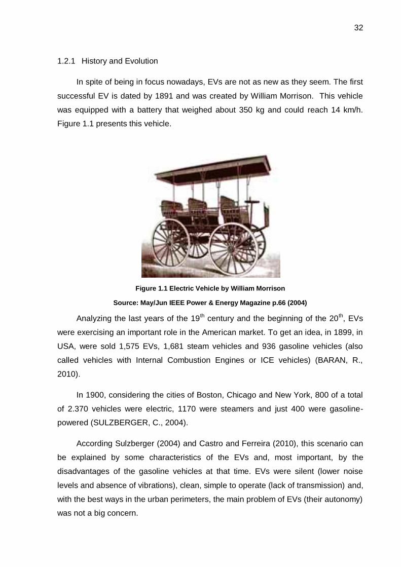
1.2.1 History and Evolution
In spite of being in focus nowadays, EVs are not as new as they seem. The first
successful EV is dated by 1891 and was created by William Morrison. This vehicle
was equipped with a battery that weighed about 350 kg and could reach 14 km/h.
Figure 1.1 presents this vehicle.
Figure 1.1 Electric Vehicle by William Morrison
Source: May/Jun IEEE Power & Energy Magazine p.66 (2004)
Analyzing the last years of the 19th century and the beginning of the 20th, EVs
were exercising an important role in the American market. To get an idea, in 1899, in
USA, were sold 1,575 EVs, 1,681 steam vehicles and 936 gasoline vehicles (also
called vehicles with Internal Combustion Engines or ICE vehicles) (BARAN, R.,
2010).
In 1900, considering the cities of Boston, Chicago and New York, 800 of a total
of 2.370 vehicles were electric, 1170 were steamers and just 400 were gasoline-
powered (SULZBERGER, C., 2004).
According Sulzberger (2004) and Castro and Ferreira (2010), this scenario can
be explained by some characteristics of the EVs and, most important, by the
disadvantages of the gasoline vehicles at that time. EVs were silent (lower noise
levels and absence of vibrations), clean, simple to operate (lack of transmission) and,
with the best ways in the urban perimeters, the main problem of EVs (their autonomy)
was not a big concern.
33
On the other hand, even the gasoline vehicles presenting some advantages
(they could travel fast, could be equipped with powerful engines and had a great
range due to the easy access to gasoline), they were noisy, smelly and polluting. To
start them, they had to be cranked by hand, process that required a strong arm and
often resulted in injuries to the handler (SULZBERGER, C., 2004).
However, this scenario changed quickly. From 1899 to 1909, gasoline vehicles
sales grew 120 times, whereas the EVs sales just doubled. With that, in 1912 the
fleet of gasoline vehicles was already 30 times bigger than the EVs fleet in New York
(BARAN, R., 2012).
For Baran (2012), the EVs fast decline occurred, mainly, due to the following
factors:
In 1912, with the invention of the electric starting and, consequently, the
abolishing of the manual starting in gasoline vehicles, the starting process on
those vehicles was not a problem anymore;
The discovery of oil reserves dropped the gasoline price;
In 1920, the roads in USA already interconnected a lot of cities, then,
vehicles capable to travel long distances were necessaries;
The production series system, idealized by Henry Ford, allowed the reduction
of the gasoline vehicles price, becoming them very much cheaper than EVs.
With the fast technological development of gasoline vehicles and with the EVs
still stuck to the slow development of batteries, the industry of gasoline vehicles
continued to grow, and EVs were almost forgotten. Their production was reduced
drastically and their use was limited just a few applications, such as trash collecting
and delivery service (BARAN, R., 2012).
Thus, the EVs remained neglected until the 1970s, when, with the oil crises and
the public opinion starting to concern about the environmental and the use of
renewable energies, the major automakers looked back to EVs. However, the
technological development in EVs was still a big impediment, preventing the
developed prototypes to achieve a satisfactory stage and, consequently, the
production lines.
34
Nevertheless, in the early of the 1990s, with the sustainable development
concept even bigger than in the 1970s and with the progress of the batteries
development, the attention came back to EVs. In USA, authorities from California
decided that the automakers from that state should provide EVs to the costumers
and the California Air Resources Board (CARB), government sector responsible for
monitoring the air quality, defined a quota of Zero Emission Vehicles (ZEV) sales of
2% in 1998, increasing to 5% in 2001 and 10% in 2003, with bonus to the
automakers for achieving this goal (BARAN, R., 2012). Even so, some sectors,
specially the major oil companies, were still reluctant to the EVs implementation.
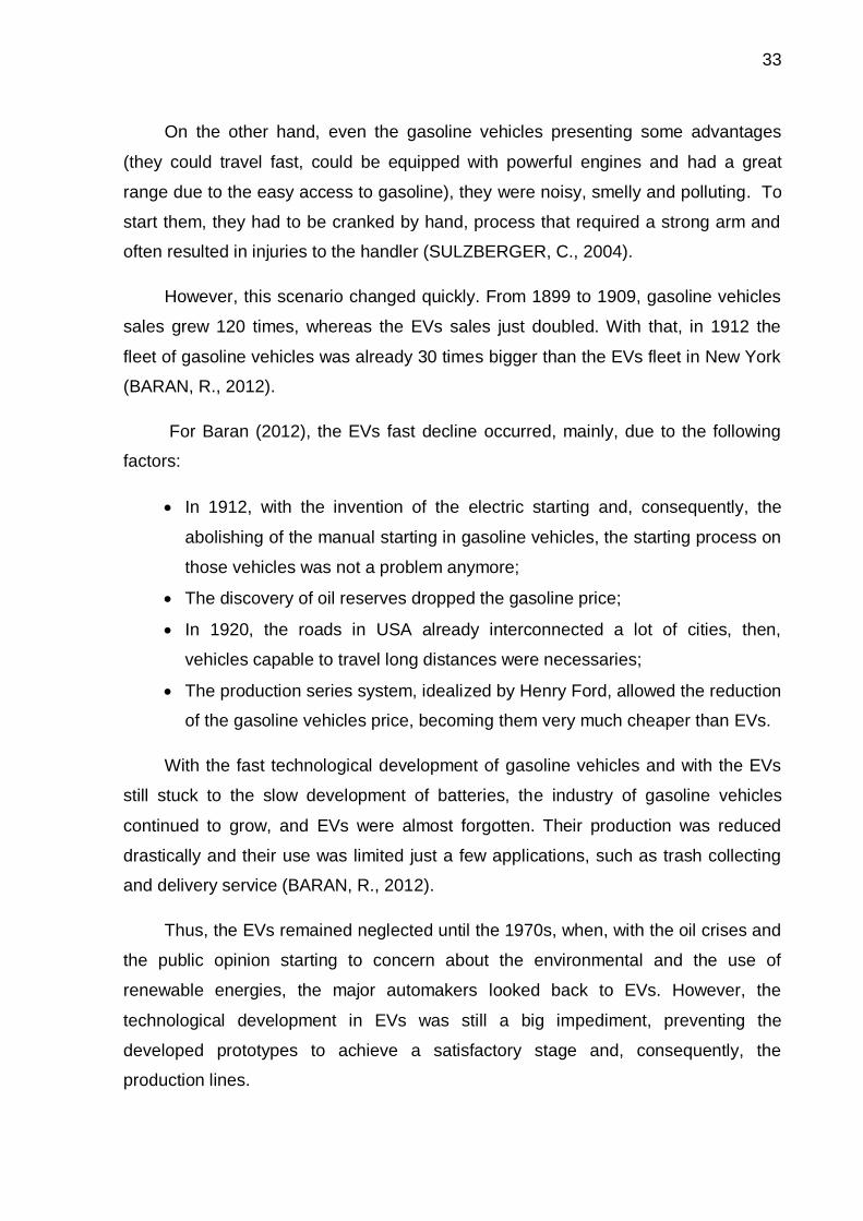
Combining these 2 situations, the Hybrid Electric Vehicles (HEVs) came to the
spotlight. Hybrid vehicles combine, at the same time, an electric motor and an ICE.
This way, the advantages from each technology can be combined, remediating the
previous problems from each one. Then, in 1997, the Toyota launched to the market
the HEV Toyota Prius. In 2000, the Toyota Prius arrived to USA, reaching high sales
rates, confirming the importance of investments and researches in this area.
Figure 1.2 Hybrid Vehicle Toyota Prius
Source: Internet image
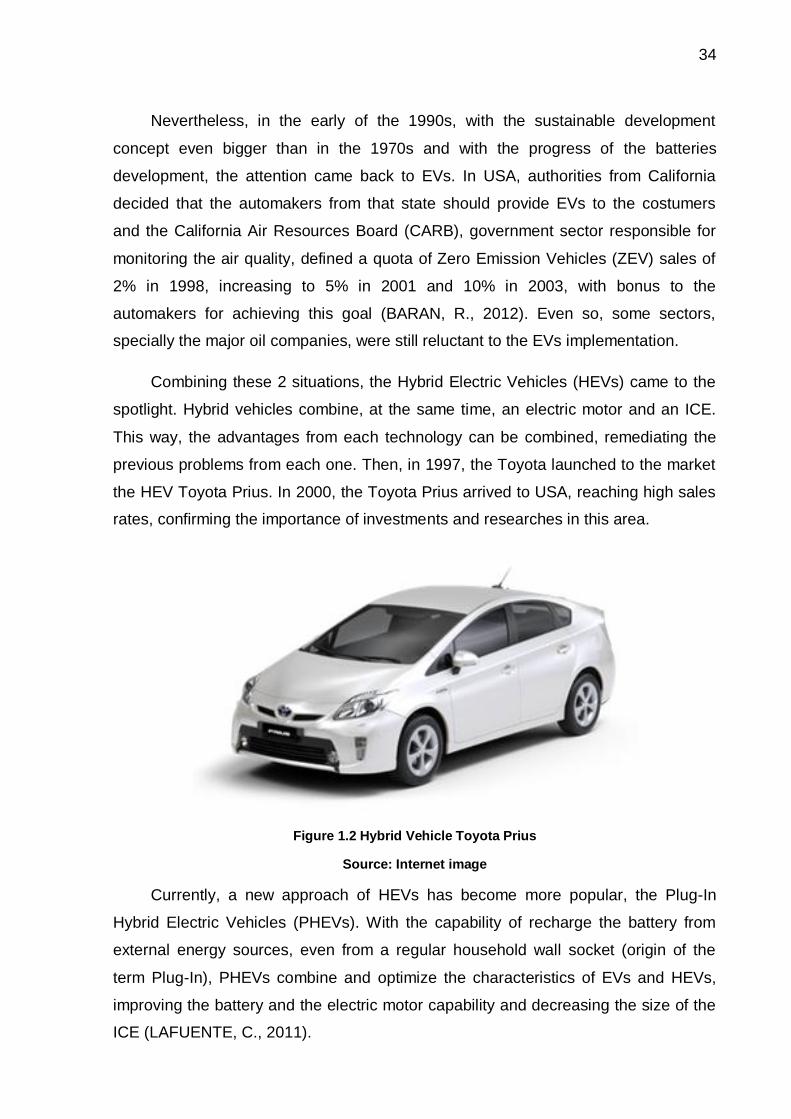
Currently, a new approach of HEVs has become more popular, the Plug-In
Hybrid Electric Vehicles (PHEVs). With the capability of recharge the battery from
external energy sources, even from a regular household wall socket (origin of the
term Plug-In), PHEVs combine and optimize the characteristics of EVs and HEVs,
improving the battery and the electric motor capability and decreasing the size of the
ICE (LAFUENTE, C., 2011).
35
Electric
Motor
ICE
Battery
Bank
Gas
Tank
Power
Electronics
Figure 1.3 Inside view of a PHEV
Source: Adapted from Lafuente, C. (2011), p. 6
1.2.2 Current Prospects
Even EVs not being a recent technology, the new generation of costumers sees
them as a novelty. However, they still suffer some distrust from costumers and,
added to questions like lack of infrastructure and technological development, their
insertion in the market is difficult.
Castro and Ferreira (2010) point another factor that has a huge influence in the
EVs insertion in the market: the size and the profile of the vehicles fleet from a
country is directly related to its economical development. That is, when a country
faces low development levels, the vehicular fleet grows slowly and the costumers
keep conservatives. Whereas the personal income of this country rises, the fleet will
grow significantly and the costumers are more open to new possibilities (change the
conventional vehicles for EVs).
Taking these situations into account, to enable the insertion of EVs and
consequently their acceptance and success in the market, government actions are
essential.
According Castro and Ferreira (2010), countries like USA, Canada, China,
Japan and Germany, among others, are investing in five basic incentives to raise the
interest for EVs. They are:
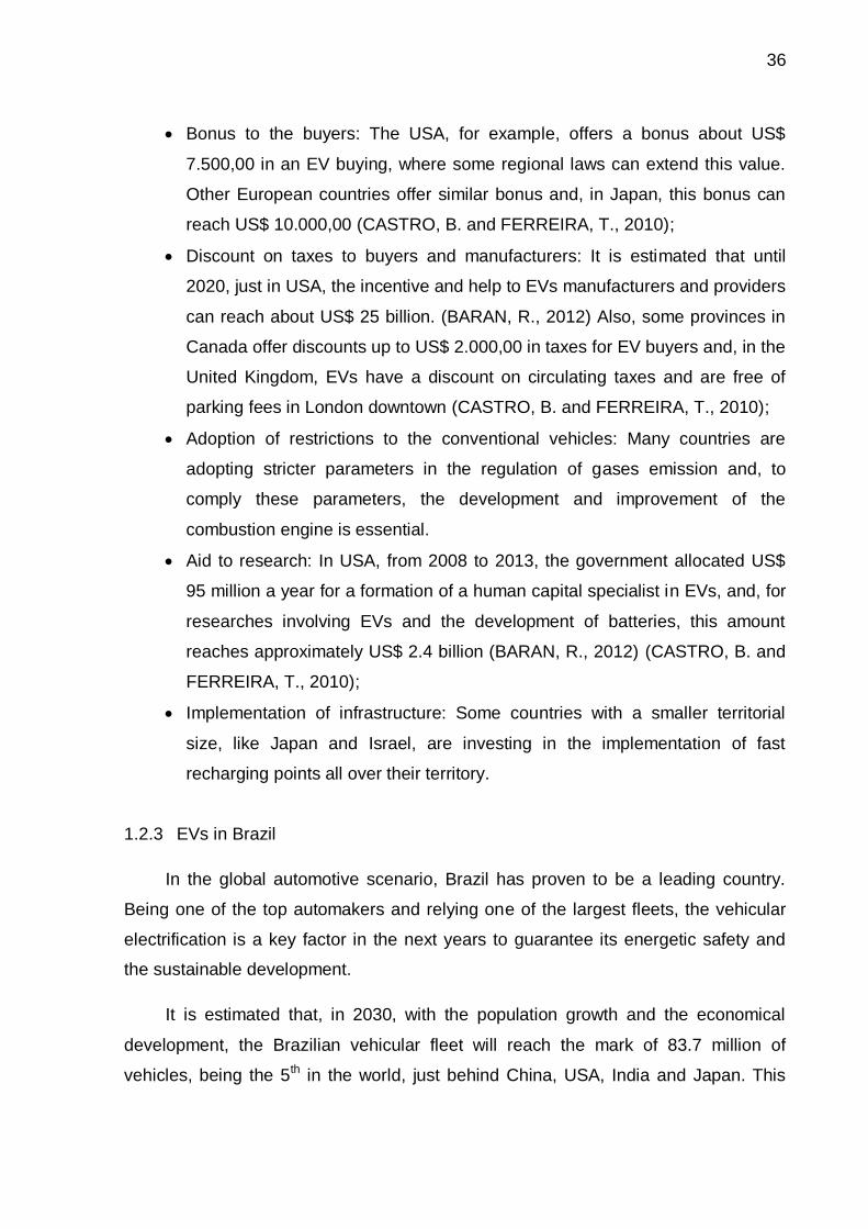
36
Bonus to the buyers: The USA, for example, offers a bonus about US$
7.500,00 in an EV buying, where some regional laws can extend this value.
Other European countries offer similar bonus and, in Japan, this bonus can
reach US$ 10.000,00 (CASTRO, B. and FERREIRA, T., 2010);
Discount on taxes to buyers and manufacturers: It is estimated that until
2020, just in USA, the incentive and help to EVs manufacturers and providers
can reach about US$ 25 billion. (BARAN, R., 2012) Also, some provinces in
Canada offer discounts up to US$ 2.000,00 in taxes for EV buyers and, in the
United Kingdom, EVs have a discount on circulating taxes and are free of
parking fees in London downtown (CASTRO, B. and FERREIRA, T., 2010);
Adoption of restrictions to the conventional vehicles: Many countries are
adopting stricter parameters in the regulation of gases emission and, to
comply these parameters, the development and improvement of the
combustion engine is essential.
Aid to research: In USA, from 2008 to 2013, the government allocated US$
95 million a year for a formation of a human capital specialist in EVs, and, for
researches involving EVs and the development of batteries, this amount
reaches approximately US$ 2.4 billion (BARAN, R., 2012) (CASTRO, B. and
FERREIRA, T., 2010);
Implementation of infrastructure: Some countries with a smaller territorial
size, like Japan and Israel, are investing in the implementation of fast
recharging points all over their territory.
1.2.3 EVs in Brazil
In the global automotive scenario, Brazil has proven to be a leading country.
Being one of the top automakers and relying one of the largest fleets, the vehicular
electrification is a key factor in the next years to guarantee its energetic safety and
the sustainable development.
It is estimated that, in 2030, with the population growth and the economical
development, the Brazilian vehicular fleet will reach the mark of 83.7 million of
vehicles, being the 5th in the world, just behind China, USA, India and Japan. This
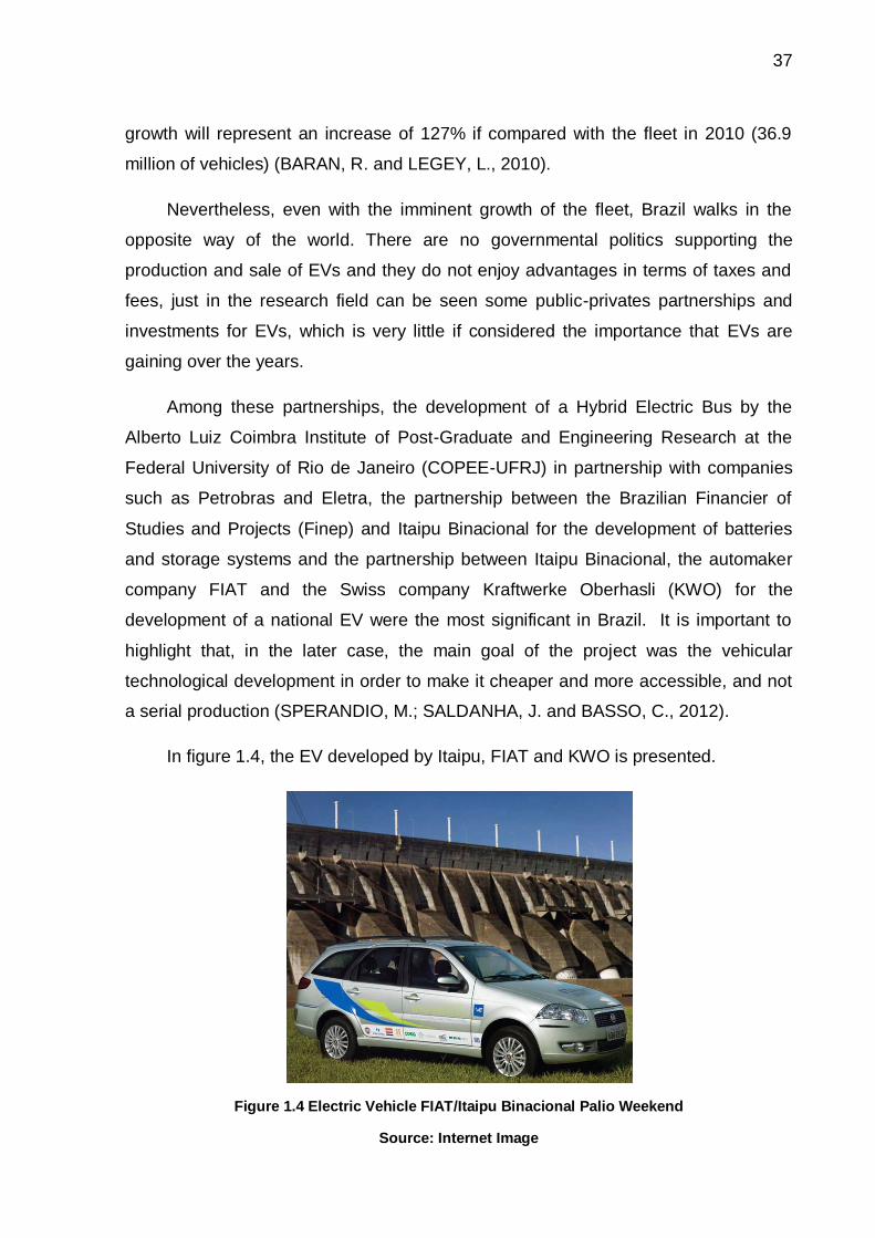
37
growth will represent an increase of 127% if compared with the fleet in 2010 (36.9
million of vehicles) (BARAN, R. and LEGEY, L., 2010).
Nevertheless, even with the imminent growth of the fleet, Brazil walks in the
opposite way of the world. There are no governmental politics supporting the
production and sale of EVs and they do not enjoy advantages in terms of taxes and
fees, just in the research field can be seen some public-privates partnerships and
investments for EVs, which is very little if considered the importance that EVs are
gaining over the years.
Among these partnerships, the development of a Hybrid Electric Bus by the
Alberto Luiz Coimbra Institute of Post-Graduate and Engineering Research at the
Federal University of Rio de Janeiro (COPEE-UFRJ) in partnership with companies
such as Petrobras and Eletra, the partnership between the Brazilian Financier of
Studies and Projects (Finep) and Itaipu Binacional for the development of batteries
and storage systems and the partnership between Itaipu Binacional, the automaker
company FIAT and the Swiss company Kraftwerke Oberhasli (KWO) for the
development of a national EV were the most significant in Brazil. It is important to
highlight that, in the later case, the main goal of the project was the vehicular
technological development in order to make it cheaper and more accessible, and not
a serial production (SPERANDIO, M.; SALDANHA, J. and BASSO, C., 2012).
In figure 1.4, the EV developed by Itaipu, FIAT and KWO is presented.
Figure 1.4 Electric Vehicle FIAT/Itaipu Binacional Palio Weekend
Source: Internet Image

38
Also, some public calls from the Brazilian National Council of Technological and
Scientific Development (CNPq-Brazil) for projects related to the development of EVs
technology were relevant in the research field.
Another factor that is directly related to the successful insertion of EVs in the
Brazilian market is the support of the National Bank for Economic and Social
Development (BNDES), the main long-term credit provider in Brazil. Actions such as
a massive marketing for EVs as the technological solution for environmental and
transportation issues, support for technological development and production line
implementation would be a first step in the EVs expansion (CASTRO, B. and
FERREIRA, T., 2010).
Also, the influence of the BNDES in the Flex Fuel Vehicles development can be
used as parameter for EVs, where, with the implementation of the actions mentioned
above in the beginning of their development, they were able to structure themselves
and become the most popular vehicular technology in Brazil.
1.3 BATTERIES
Basically, batteries, also called electric accumulators, are devices that convert
chemical energy in electrical energy through a phenomenon known as electrolysis.
The first record of an electric accumulator is dated by 250 B.C., in Syria, where
a ceramic container with an iron bar surrounded by a copper cylinder could produce
around 1.1 Vdc when full of vinegar (LAFUENTE, C., 2011). Figure 1.5 presents this
device.
However, the landmark of the batteries’ history occurred just in 1800, when
Alessandro Volta, based on the work of Luigi Galvani about animal electricity,
discovered the electrolysis principle and developed the first battery.
In 1859, the French physicist Gastón Plante developed the first Pb-acid
rechargeable battery (LAFUENTE, C., 2011). However, according Sulzberger (2004),
early Pb-acid batteries were heavy, difficult to recharge, very corrosive, and
presented a low power density, around 4 – 6 W/h, requiring approximately between
56 and 80 kg of battery for 0.745 kW/h at the battery terminals. Since then, the Pb-
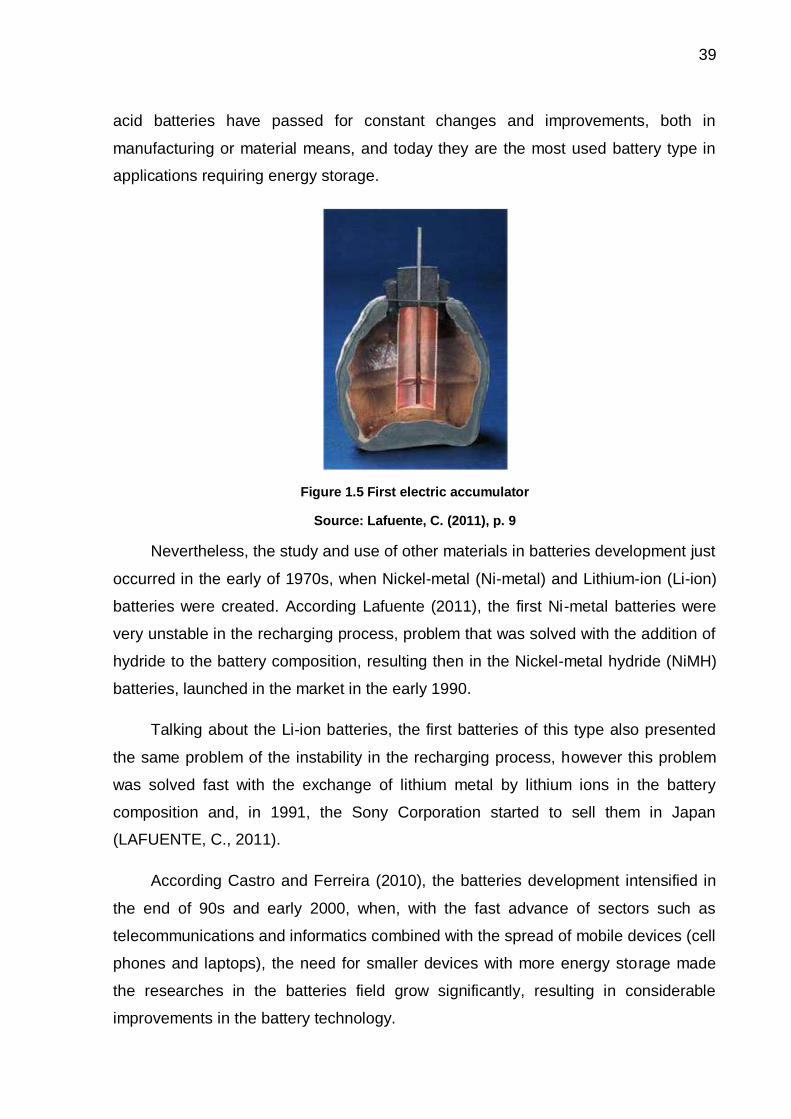
39
acid batteries have passed for constant changes and improvements, both in
manufacturing or material means, and today they are the most used battery type in
applications requiring energy storage.
Figure 1.5 First electric accumulator
Source: Lafuente, C. (2011), p. 9
Nevertheless, the study and use of other materials in batteries development just
occurred in the early of 1970s, when Nickel-metal (Ni-metal) and Lithium-ion (Li-ion)
batteries were created. According Lafuente (2011), the first Ni-metal batteries were
very unstable in the recharging process, problem that was solved with the addition of
hydride to the battery composition, resulting then in the Nickel-metal hydride (NiMH)
batteries, launched in the market in the early 1990.
Talking about the Li-ion batteries, the first batteries of this type also presented
the same problem of the instability in the recharging process, however this problem
was solved fast with the exchange of lithium metal by lithium ions in the battery
composition and, in 1991, the Sony Corporation started to sell them in Japan
(LAFUENTE, C., 2011).
According Castro and Ferreira (2010), the batteries development intensified in
the end of 90s and early 2000, when, with the fast advance of sectors such as
telecommunications and informatics combined with the spread of mobile devices (cell
phones and laptops), the need for smaller devices with more energy storage made
the researches in the batteries field grow significantly, resulting in considerable
improvements in the battery technology.
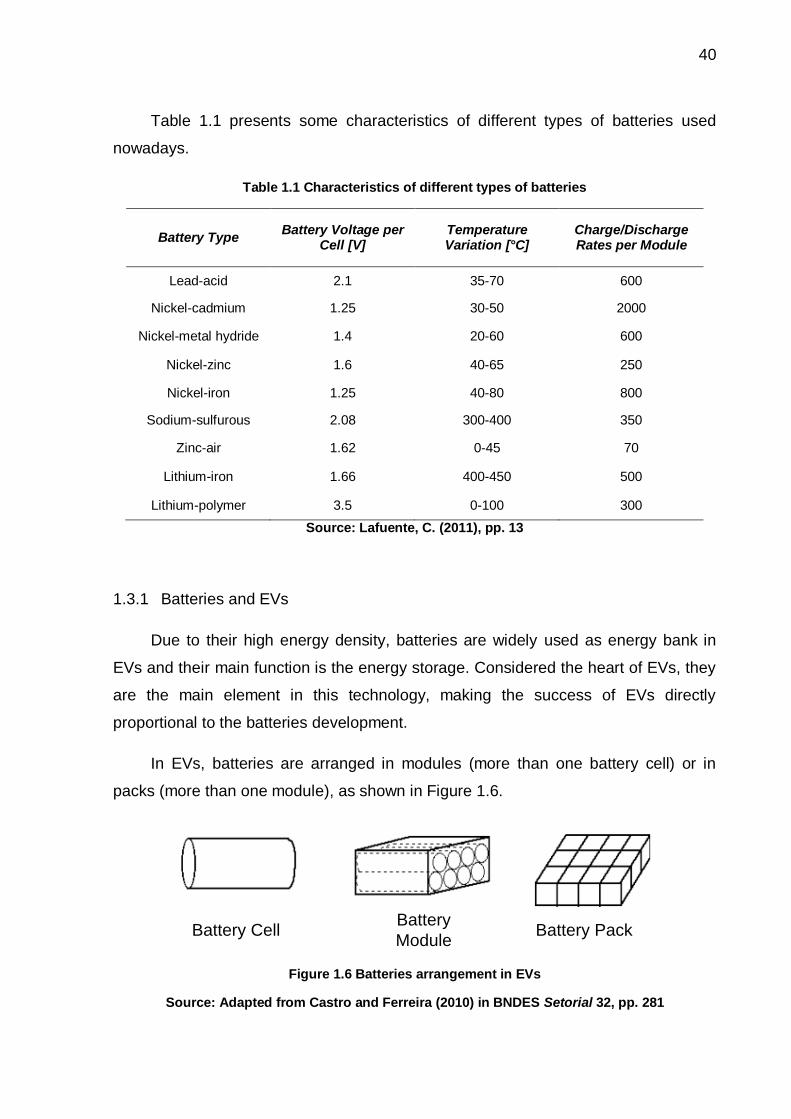
40
Table 1.1 presents some characteristics of different types of batteries used
nowadays.
Table 1.1 Characteristics of different types of batteries
Battery Type Battery Voltage per
Cell [V] Temperature Variation [°C]
Charge/Discharge Rates per Module
Lead-acid 2.1 35-70 600
Nickel-cadmium 1.25 30-50 2000
Nickel-metal hydride 1.4 20-60 600
Nickel-zinc 1.6 40-65 250
Nickel-iron 1.25 40-80 800
Sodium-sulfurous 2.08 300-400 350
Zinc-air 1.62 0-45 70
Lithium-iron 1.66 400-450 500
Lithium-polymer 3.5 0-100 300
Source: Lafuente, C. (2011), pp. 13
1.3.1 Batteries and EVs
Due to their high energy density, batteries are widely used as energy bank in
EVs and their main function is the energy storage. Considered the heart of EVs, they
are the main element in this technology, making the success of EVs directly
proportional to the batteries development.
In EVs, batteries are arranged in modules (more than one battery cell) or in
packs (more than one module), as shown in Figure 1.6.
Battery CellBattery
ModuleBattery Pack
Figure 1.6 Batteries arrangement in EVs
Source: Adapted from Castro and Ferreira (2010) in BNDES Setorial 32, pp. 281
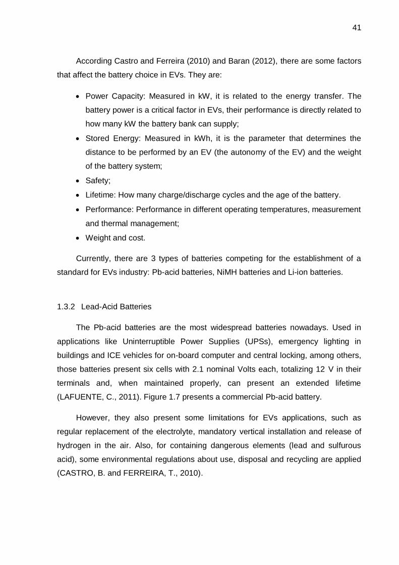
41
According Castro and Ferreira (2010) and Baran (2012), there are some factors
that affect the battery choice in EVs. They are:
Power Capacity: Measured in kW, it is related to the energy transfer. The
battery power is a critical factor in EVs, their performance is directly related to
how many kW the battery bank can supply;
Stored Energy: Measured in kWh, it is the parameter that determines the
distance to be performed by an EV (the autonomy of the EV) and the weight
of the battery system;
Safety;
Lifetime: How many charge/discharge cycles and the age of the battery.
Performance: Performance in different operating temperatures, measurement
and thermal management;
Weight and cost.
Currently, there are 3 types of batteries competing for the establishment of a
standard for EVs industry: Pb-acid batteries, NiMH batteries and Li-ion batteries.
1.3.2 Lead-Acid Batteries
The Pb-acid batteries are the most widespread batteries nowadays. Used in
applications like Uninterruptible Power Supplies (UPSs), emergency lighting in
buildings and ICE vehicles for on-board computer and central locking, among others,
those batteries present six cells with 2.1 nominal Volts each, totalizing 12 V in their
terminals and, when maintained properly, can present an extended lifetime
(LAFUENTE, C., 2011). Figure 1.7 presents a commercial Pb-acid battery.
However, they also present some limitations for EVs applications, such as
regular replacement of the electrolyte, mandatory vertical installation and release of
hydrogen in the air. Also, for containing dangerous elements (lead and sulfurous
acid), some environmental regulations about use, disposal and recycling are applied
(CASTRO, B. and FERREIRA, T., 2010).
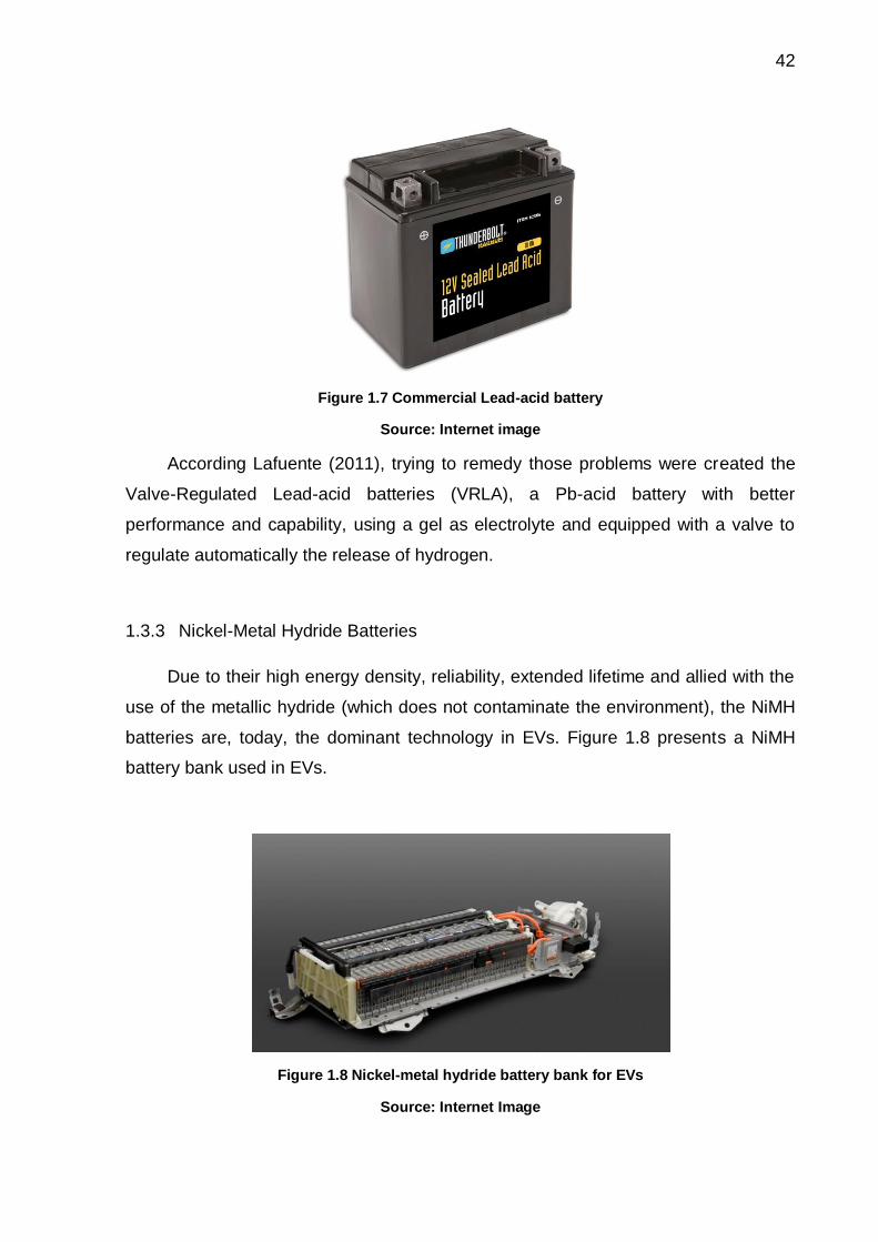
42
Figure 1.7 Commercial Lead-acid battery
Source: Internet image
According Lafuente (2011), trying to remedy those problems were created the
Valve-Regulated Lead-acid batteries (VRLA), a Pb-acid battery with better
performance and capability, using a gel as electrolyte and equipped with a valve to
regulate automatically the release of hydrogen.
1.3.3 Nickel-Metal Hydride Batteries
Due to their high energy density, reliability, extended lifetime and allied with the
use of the metallic hydride (which does not contaminate the environment), the NiMH
batteries are, today, the dominant technology in EVs. Figure 1.8 presents a NiMH
battery bank used in EVs.
Figure 1.8 Nickel-metal hydride battery bank for EVs
Source: Internet Image

43
Nevertheless, limitations such as high cost (due to the elevated use of nickel),
weight, heat losses causing a decrement in the efficiency and periodic maintenance
are some factors that do not allow these batteries a more significant market
conquest.
It is important to highlight that, according Baran (2012), there is no expectation
of a growth in the use and technological development of NiMH batteries, while they
have practically reached their maximum point of development.
1.3.4 Lithium-Ion Batteries
Nowadays, due to the potential and success already presented in the electronic
industry, telecommunication applications and mobile devices, the Li-ion batteries are
the biggest bet for the development and future of EVs. Besides, the lithium is not
toxic and is a cheap raw material.
The Li-ion batteries are formed, basically, by an anode (negative electrode)
usually made of graphite and a cathode (positive electrode) usually derived from
Lithium Carbonate (Li3CO3) or Lithium Hydroxide (LiOH). It is estimated that the
cathodes represent 40% of the battery cost. Among the different types of Lithium
batteries, some can be highlighted: the Lithium-Nickel-Cobalt-Aluminum batteries
(NCA); the Lithium-Nickel-Manganese-Cobalt batteries (NMC) and the Lithium-Iron-
Phosphate batteries (LFP) (CASTRO, B. and FERREIRA, T., 2010).
Figure 1.9 presents a Li-ion battery module for EVs.
Figure 1.9 Lithium-ion battery module for EVs
Source: Lafuente, C. (2011), pp. 17
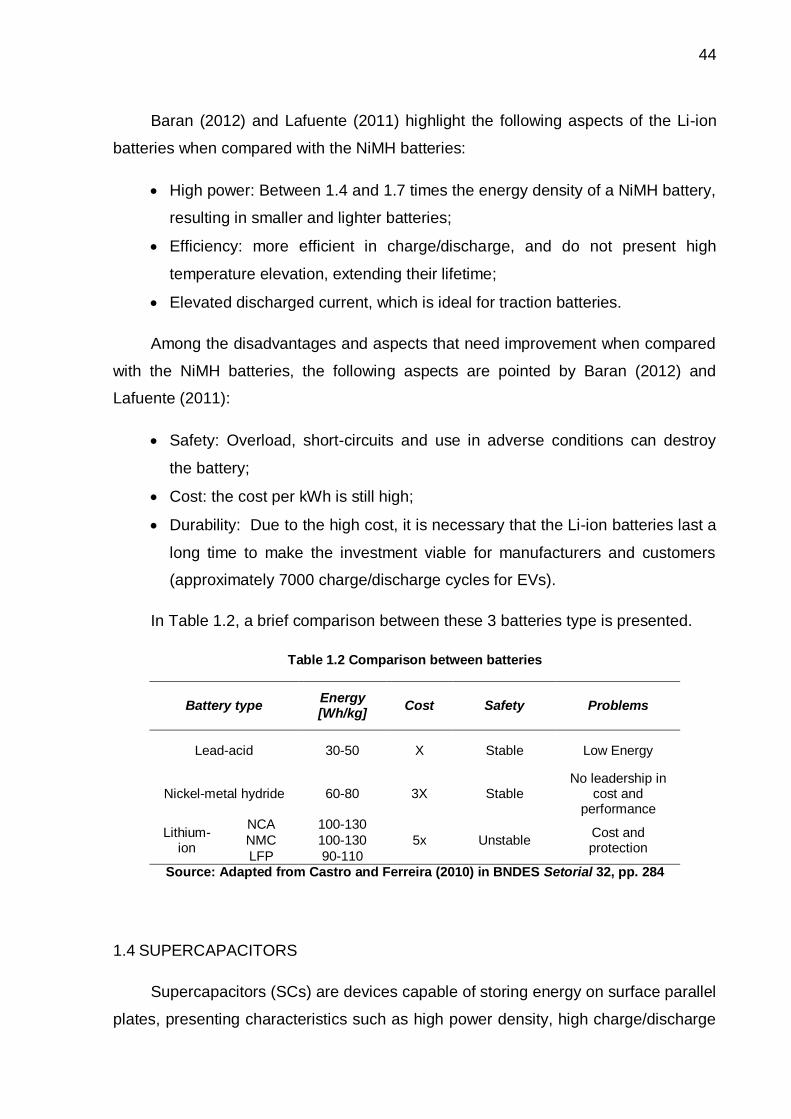
44
Baran (2012) and Lafuente (2011) highlight the following aspects of the Li-ion
batteries when compared with the NiMH batteries:
High power: Between 1.4 and 1.7 times the energy density of a NiMH battery,
resulting in smaller and lighter batteries;
Efficiency: more efficient in charge/discharge, and do not present high
temperature elevation, extending their lifetime;
Elevated discharged current, which is ideal for traction batteries.
Among the disadvantages and aspects that need improvement when compared
with the NiMH batteries, the following aspects are pointed by Baran (2012) and
Lafuente (2011):
Safety: Overload, short-circuits and use in adverse conditions can destroy
the battery;
Cost: the cost per kWh is still high;
Durability: Due to the high cost, it is necessary that the Li-ion batteries last a
long time to make the investment viable for manufacturers and customers
(approximately 7000 charge/discharge cycles for EVs).
In Table 1.2, a brief comparison between these 3 batteries type is presented.
Table 1.2 Comparison between batteries
Battery type Energy [Wh/kg]
Cost Safety Problems
Lead-acid 30-50 X Stable Low Energy
Nickel-metal hydride 60-80 3X Stable No leadership in
cost and performance
Lithium-ion
NCA 100-130
5x Unstable Cost and protection
NMC 100-130
LFP 90-110 Source: Adapted from Castro and Ferreira (2010) in BNDES Setorial 32, pp. 284
1.4 SUPERCAPACITORS
Supercapacitors (SCs) are devices capable of storing energy on surface parallel
plates, presenting characteristics such as high power density, high charge/discharge
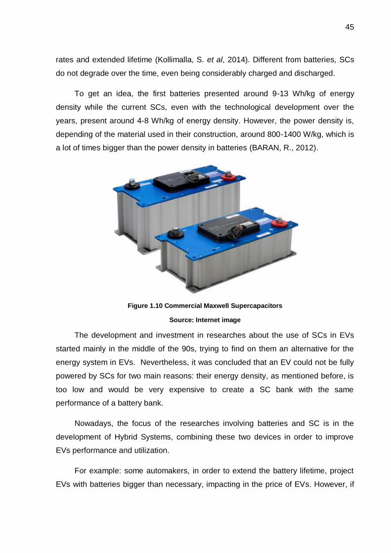
45
rates and extended lifetime (Kollimalla, S. et al, 2014). Different from batteries, SCs
do not degrade over the time, even being considerably charged and discharged.
To get an idea, the first batteries presented around 9-13 Wh/kg of energy
density while the current SCs, even with the technological development over the
years, present around 4-8 Wh/kg of energy density. However, the power density is,
depending of the material used in their construction, around 800-1400 W/kg, which is
a lot of times bigger than the power density in batteries (BARAN, R., 2012).
Figure 1.10 Commercial Maxwell Supercapacitors
Source: Internet image
The development and investment in researches about the use of SCs in EVs
started mainly in the middle of the 90s, trying to find on them an alternative for the
energy system in EVs. Nevertheless, it was concluded that an EV could not be fully
powered by SCs for two main reasons: their energy density, as mentioned before, is
too low and would be very expensive to create a SC bank with the same
performance of a battery bank.
Nowadays, the focus of the researches involving batteries and SC is in the
development of Hybrid Systems, combining these two devices in order to improve
EVs performance and utilization.
For example: some automakers, in order to extend the battery lifetime, project
EVs with batteries bigger than necessary, impacting in the price of EVs. However, if
46
used in conjunction with SCs, the battery bank size can be reduced and, at the same
time, it is allowed better energy storage for the batteries.
1.5 HYBRID ENERGY STORAGE SYSTEMS
According Bocklisch (2015), a Hybrid Energy Storage System (HESS) can be
characterized by a beneficial combination of two or more different energy sources
with supplementary operating characteristics (energy and power density, self-
discharge rate, efficiency, lifetime, etc). On simpler words, a HESS combines
different energy sources in order to create a new system capable to provide the
benefits of each energy source.
In a HESS, one of the energy sources must be characterized by fast response
time, high efficiency and lifetime, being responsible to supply the high power
demand, transients and the fast load fluctuations of the system. On the other hand,
the other energy source will be responsible to supply the high energy demand of the
system, commonly presenting characteristics like low self-discharge rates (Bocklisch,
T., 2015).
According Bocklisch (2015), a HESS presents the following main advantages:
Reduction of total investment costs if compared to a single storage system;
Efficiency increasing of the system;
Increase of energy storage and lifetime.
Currently, HESS are being strongly used in applications like renewable energy
systems, smart grids and EVs, employing different energy sources such as batteries,
SCs and fuel cells, among others.
To make the implementation of a HESS possible, there are different ways to
make the coupling of the storage units. The simplest way is the direct coupling of the
storages, presenting the simplicity and low costs of implementation as the main
advantage of this configuration. However, the possibilities of power flow control
become reduced, resulting in an ineffective utilization of the storage units.
Another energy storage coupling architecture possible is via a bidirectional DC-
DC converter interfacing the storage units. In this case, the bidirectional DC-DC

47
converter will allow the power flow control in the HESS, resulting in an optimization of
the power management in the HESS, protecting the high-energy storage unit against
peak power and fast load fluctuations. The drawback of this solution, according
Bocklisch (2015), is the fluctuation of the DC Bus voltage.
Talking specifically about EVs, the later architecture with a bidirectional DC-DC
converter interfacing a battery bank and a SC is the most common nowadays, being
the focus of different researches for the EVs energy system.
1.5.1 Battery/Supercapacitor Hybrid Energy Storage System
As mentioned before, the Battery/SC HESS with a bidirectional DC-DC
converter interfacing the battery and the SC is the most recent focus of research
involving EVs energy bank. Figure 1.11 presents the schematic of the
implementation of a Battery/SC HESS in EVs.
DC BUS
Icond ISC
IBatteryBidirectional
DC-DC
ConverterVB VSC
Motor
DC-AC
Converter
Traction
System
HESS
Figure 1.11 Battery/Supercapacitor HESS in EVs applications
Source: Self Authorship
In this configuration, the SC can act like a buffer against large magnitudes and
rapid fluctuations in the power, improving the system performance. Among some
characteristics of the Battery/SC HESS, the following can be highlighted:
Improvement of the battery lifetime;
Reduction of the stress on batteries;
Reduction in the battery size/cost;
48
Improvement in power management (generation/demand);
Battery supports slow transients whereas the SC supports the fast;
SC can recover more energy from the regenerative breaking.
Currently, there are different topologies of bidirectional DC-DC converters and
control modes for a HESS implementation, themes that are going to be discussed in
the next chapter.
1.6 CHAPTER CONCLUSION
In this chapter, the topics that hold the proposal of application addressed in this
work, such as EVs and some of their energy system elements, were presented and
discussed.
As shown in chapter 1, EVs are not a recent technology as many people believe
they are and even them presenting considerable advantages when compared to ICE
vehicles, issues such as lack of infrastructure, distrust of costumers and
technological barriers are some of the reasons why EVs do not achieve a significant
market conquest.
In this scenario, government actions and massive support to research have
been shown to be essential for breaking down these barriers and, consequently, to
allow the growth and expansion of EVs.
49
CHAPTER 2
BIDIRECTIONAL DC-DC CONVERTERS
2.1 CHAPTER INTRODUCTION
In this chapter, a brief review of DC-DC converters is presented. Considering
the fact that the unidirectional DC-DC converters are a key element in the
development and understanding of bidirectional DC-DC converters, a review
involving the concepts and applications of those converters is carried out.
Then, bidirectional DC-DC converters are presented, discussing their role in the
power electronics scenario nowadays, presenting some concepts and applications
where they are needed. In the end, the two topologies that are references to this
work are discussed.
2.2 DC-DC CONVERTERS
Conceptually, a DC-DC converter can be defined as a system formed by power
devices, such as diodes, Metal-Oxide Field-Effect Transistors (MOSFETs) and
Insulated-Gate Bipolar Transistors (IGBTs) and passive elements, such as capacitors
and inductors (BARBI, I. and MARTINS, D., 2000).
In a DC-DC converter, a DC voltage or current level is applied in the input
terminals and, with a command strategy for the turning-on/off of the power devices,
these levels can be adjusted to desired parameters in the output terminals. In other
words, the function of a DC-DC converter is to convert energy from a DC energy
source to a DC load, where high conversion efficiency is a key factor.
The traditional DC-DC converters are characterized by having a transistor
(operating as a switch), a diode and one or more capacitors and inductors. They also
work with fixed switching frequency and variable duty cycle, presenting voltage step-
down function (Buck) or voltage step-up function (Boost) and, in some cases, both
functions (Buck-Boost).

50
Figure 2.1 presents the traditional DC-DC converters known in the literature.
V2V1 V2
++++
- -
C1 C2
L
S1
D+ +
V1
- -
C1 C2
L
S1
D
+ +
V1 V2
-+
S1
C1 C2L
D
+
+
- +
(a) (b)
(c)
Figure 2.1 Traditional DC-DC converters: (a) Buck (b) Boost (c) Buck-Boost
Source: Self Authorship
The operating principle of the topologies presented in Figure 2.1 is based on the
fact that never the transistor and the diode conduct at the same time: when the
transistor is conducting, the diode will be blocked, and when the transistor blocks the
diode starts to conduct.
DC-DC converters may also present three different operation modes, which are
characterized by the inductor current behavior: the Continuous Conduction Mode
(CCM), where the inductor current never reaches zero; the Discontinuous
Conduction Mode (DCM), where the inductor current reaches zero in more than one
instant of time and the Critical Conduction Mode (CrCM), where the current will reach
zero in a single instant of time.
DC-DC converters can also be isolated or non-isolated. The isolated converters
have a transformer on their topology, providing galvanic isolation between the source
and the load. Figure 2.2 presents some of the traditional isolated DC-DC converters.
Furthermore, the switching method is another important factor for DC-DC
converters, where they can operate with hard-switching or soft-switching. Nowadays,
with the increase appeal for high-efficiency systems, the most part of the converters
work with soft-switching.
In the soft-switching, the addition of components to the circuit or the use of
parasitic elements makes the switches of the system achieve a Zero-Voltage

51
Switching (ZVS) or a Zero-Current Switching (ZCS), increasing the efficiency of the
system. Also, with the implementation of the soft-switching, the size, weight and
volume of the system can be reduced, since with soft-switching the switching
frequency can be elevated, reducing the size of the magnetic elements (BELLUR, D.
and KAZIMIERCZUK, M., 2007).
V1
+
V2
+
V1
+
V2
+
C2C1
--
D
(a)
Tr
+ +
-
C2C1++
-
Tr D2
D3
L1
(b)
S1 D1S1
Figure 2.2 Traditional isolated DC-DC converters: (a) Flyback (b) Forward
Source: Self Authorship
2.3 BIDIRECTIONAL DC-DC CONVERTERS
Analyzing the topologies presented in Figures 2.1 and 2.2, the energy flows just
in one direction, from the voltage source 1 (V1) to the voltage source 2 (V2), and the
opposite direction is not possible. In this case, the converters are called unidirectional
converters.
Nevertheless, an increasing number of applications requiring a constant
exchange of energy from a source to a load (as motor drives, renewable energy
systems, electric vehicles, hybrid energy systems, among others), and vice versa,
makes impossible the use of unidirectional converters. In those cases, bidirectional
converters are needed, where is the bidirectional converter that will allow the energy
exchange and the power flow control in the system.
Usually, bidirectional DC-DC converters are current controlled by a PWM signal,
where the direction of the current will represent the direction of the power flow.
Because of that, they always work in CCM and there is no DCM or CrCM operation
for bidirectional DC-DC converters (CARDOSO, R., 2007).
According Khan et al (2016), the simplest and easiest way of obtaining
bidirectional DC-DC converters is to replace the diodes of the unidirectional
converters with switches having unidirectional current blocking and bidirectional

52
voltage blocking capability. Figures 2.3 and 2.4 present the bidirectional DC-DC
converters derived from unidirectional topologies.
V2V1 V2
++++
- -
C1 C2
L
S1
(a)
+ +V1
- -
C1 C2
L
S1+ +
(b)
V1 V2
-+S1
C1 C2L+
+
- +
(c)
S2
S2
S2
Figure 2.3 Traditional bidirectional DC-DC converters: (a) Buck/Boost (b) Boost/Buck (c) Buck-Boost
Source: Self Authorship
V1
+
V2
+
V1
+
V2
+
C2C1
--
(a)
Tr
+ +
-
C2C1++
-
Tr
S1
L1
(b)
S1
S2
S4
S3
S2
Figure 2.4 Traditional isolated bidirectional DC-DC converters: (a) Flyback (b) Forward
Source: Self Authorship
Over the years, more bidirectional DC-DC topologies have been studied, always
aiming to meet the demand of applications, preferably presenting high-efficiency and
different modes of operation. Following, the two topologies that are reference
topologies for the topologies addressed in this thesis are presented.
2.3.1 Integrated Bidirectional Buck/Boost/Buck-Boost DC-DC Converter
In Figure 2.5, an integrated version of the Buck, Boost and Buck-Boost
converters is presented.

53
D1 D2L
V2
+
-
V1
+
-
C1+
C2+
S1 S2
S3 D3 D4 S4
Figure 2.5 Integrated bidirectional Buck/Boost/Buck-Boost DC-DC converter
Source: Self Authorship
Introduced by Caracchi et al (1998), this topology is nowadays one of the most
used topologies when a bidirectional DC-DC converter is required, being
implemented in a wide range of applications. The main advantage of this topology is
that it can operate like a Buck, Boost or Buck-Boost for each direction of the power
flow, facilitating its application since the mentioned operations are already widely
known and studied in the literature.
With the current control of the inductor L, the power flow in the converter can be
controlled, making the exchange of energy between V1 and V2 possible. Considering
the direction of the power flow, when the converter is sending energy from V1 to V2 it
will be considered as a Forward converter and, when operating in the opposite way,
as a Reverse converter.
In Table 2.1, the switching logic for each operation mode is presented.
Table 2.1 Integrated bidirectional Buck/Boost/Buck-Boost DC-DC converter: Switching Logic
Operation Mode S1 S2 S3 S4
Forward Buck PWM OFF OFF OFF
Forward Boost ON OFF OFF PWM
Forward Buck-Boost PWM OFF OFF PWM
Reverse Buck OFF PWM OFF OFF
Reverse Boost OFF ON PWM OFF
Reverse Buck-Boost OFF PWM PWM OFF
Source: Self Authorship
Considering the switching logic presented in Table 2.1, in Figures 2.6 and 2.7
are presented the operating stages of the integrated bidirectional Buck/Boost/Buck-
Boost converter for each power flow direction.
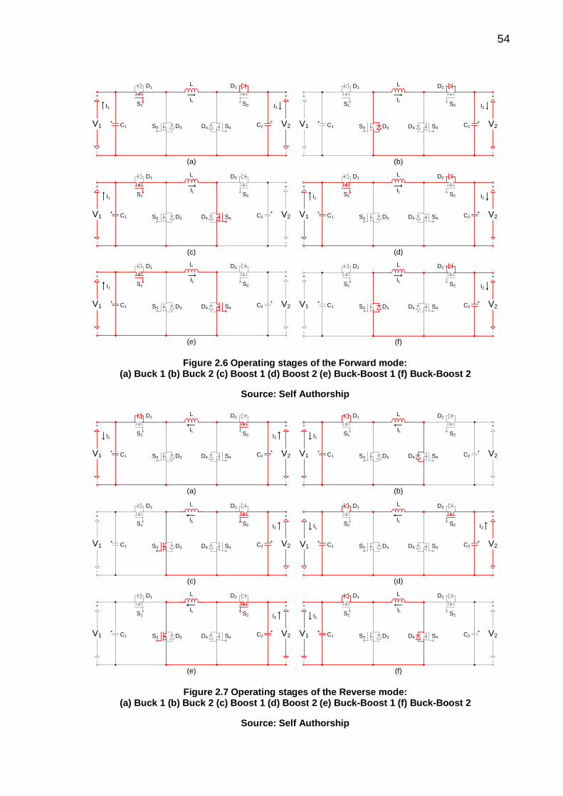
54
D1 D2L
V2
+
-
V1
+
-
C1+
C2+
S1 S2
S3 D3 D4 S4
(a)
ILI2I1
D1 D2L
V2
+
-
V1
+
-
C1+
C2+
S1 S2
S3 D3 D4 S4
(d)
ILI2I1
D1 D2L
V2
+
-
V1
+
-
C1+
C2+
S1 S2
S3 D3 D4 S4
(c)
ILI1
D1 D2L
V2
+
-
V1
+
-
C1+
C2+
S1 S2
S3 D3 D4 S4
(e)
ILI1
D1 D2L
V2
+
-
V1
+
-
C1+
C2+
S1 S2
S3 D3 D4 S4
(b)
ILI2
D1 D2L
V2
+
-
V1
+
-
C1+
C2+
S1 S2
S3 D3 D4 S4
(f)
ILI2
Figure 2.6 Operating stages of the Forward mode: (a) Buck 1 (b) Buck 2 (c) Boost 1 (d) Boost 2 (e) Buck-Boost 1 (f) Buck-Boost 2
Source: Self Authorship
V1
+
D1 D2L
V2
+
--
C1+
C2+
S1 S2
S3 D3 D4 S4
(a)
ILI2I1
D1 D2L
V2
+
--
C1+
C2+
S1 S2
S3 D3 D4 S4
(d)
ILI2I1
D1 D2L
V2
+
-
V1
+
-
C1+
C2+
S1 S2
S3 D3 D4 S4
(c)
ILI2
D1 D2L
V2
+
-
V1
+
-
C1+
C2+
S1 S2
S3 D3 D4 S4
(e)
ILI2
D1 D2L
V2
+
-
V1
+
-
C1+
C2+
S1 S2
S3 D3 D4 S4
(b)
ILI1
D1 D2L
V2
+
-
V1
+
-
C1+
C2+
S1 S2
S3 D3 D4 S4
(f)
ILI1
V1
Figure 2.7 Operating stages of the Reverse mode: (a) Buck 1 (b) Buck 2 (c) Boost 1 (d) Boost 2 (e) Buck-Boost 1 (f) Buck-Boost 2
Source: Self Authorship
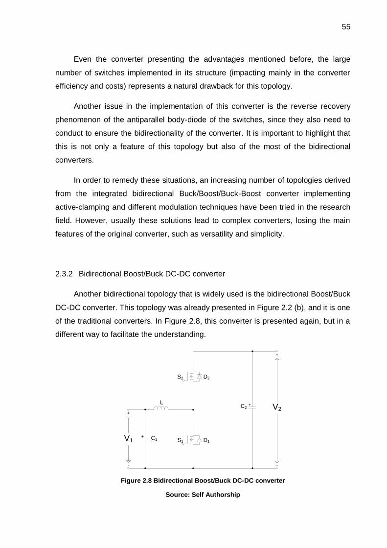
55
Even the converter presenting the advantages mentioned before, the large
number of switches implemented in its structure (impacting mainly in the converter
efficiency and costs) represents a natural drawback for this topology.
Another issue in the implementation of this converter is the reverse recovery
phenomenon of the antiparallel body-diode of the switches, since they also need to
conduct to ensure the bidirectionality of the converter. It is important to highlight that
this is not only a feature of this topology but also of the most of the bidirectional
converters.
In order to remedy these situations, an increasing number of topologies derived
from the integrated bidirectional Buck/Boost/Buck-Boost converter implementing
active-clamping and different modulation techniques have been tried in the research
field. However, usually these solutions lead to complex converters, losing the main
features of the original converter, such as versatility and simplicity.
2.3.2 Bidirectional Boost/Buck DC-DC converter
Another bidirectional topology that is widely used is the bidirectional Boost/Buck
DC-DC converter. This topology was already presented in Figure 2.2 (b), and it is one
of the traditional converters. In Figure 2.8, this converter is presented again, but in a
different way to facilitate the understanding.
V1
-
+
+C2 V2
-
S1 D1
S2 D2
L
+
+ C1
Figure 2.8 Bidirectional Boost/Buck DC-DC converter
Source: Self Authorship

56
Due to its simple arrangement and employing few power elements, this
converter is considered one of the most reliable bidirectional DC-DC converters,
being used in different applications and power levels (MAYER, R. et al, 2015).
In the same way of the converter presented in Figure 2.5, with the current
control of the inductor L, the power flow in the system becomes controllable.
Nevertheless, this converter can only work like a Boost in the Forward mode (V1 to
V2) and like a Buck in the Reverse mode (V2 to V1). In Table 2.2, the switching logic
of the bidirectional Boost/Buck DC-DC converter is presented, where the two
switches S1 and S2 work in a complementary way.
Table 2.2 Bidirectional Boost/Buck DC-DC converter: Switching Logic
Operation Mode S1 S2
Forward Boost PWM OFF
Reverse Buck OFF PWM
Source: Self Authorship
In Figure 2.9, the operating stages for each operation mode of the bidirectional
Boost/Buck DC-DC converter are presented.
V1
-
+
+C2 V2
-
S1 D1
S2 D2
L
+
+ C1
(b)
I1IL
I2
V1
-
+
+C2 V2
-
S1 D1
S2 D2
L
+
+ C1
(a)
I1IL
V1
-
+
+C2 V2
-
S1 D1
S2 D2
L
+
+ C1
(d)
I1IL
V1
-
+
+C2 V2
-
S1 D1
S2 D2
L
+
+ C1
(c)
I1IL
I2
Figure 2.9 Operating stages of the bidirectional Boost/Buck DC-DC converter: (a) Forward Boost 1 (b) Forward Boost 2 (c) Reverse Buck 1 (d) Reverse Buck 2
Source: Self Authorship
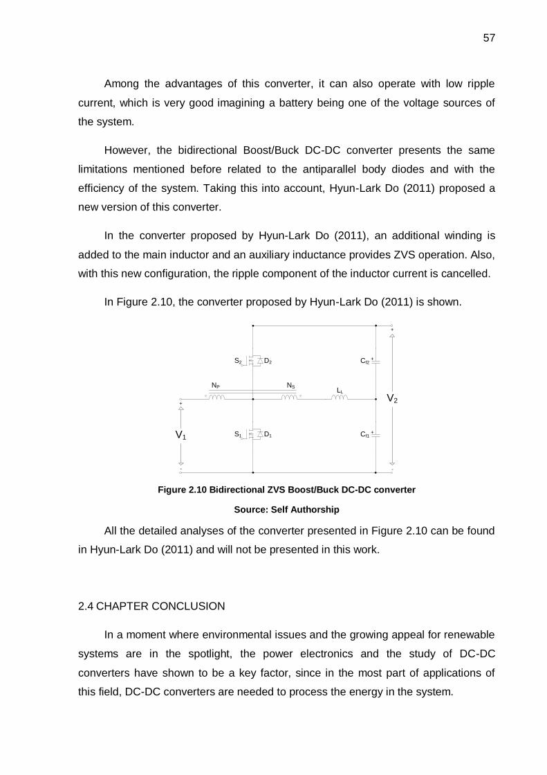
57
Among the advantages of this converter, it can also operate with low ripple
current, which is very good imagining a battery being one of the voltage sources of
the system.
However, the bidirectional Boost/Buck DC-DC converter presents the same
limitations mentioned before related to the antiparallel body diodes and with the
efficiency of the system. Taking this into account, Hyun-Lark Do (2011) proposed a
new version of this converter.
In the converter proposed by Hyun-Lark Do (2011), an additional winding is
added to the main inductor and an auxiliary inductance provides ZVS operation. Also,
with this new configuration, the ripple component of the inductor current is cancelled.
In Figure 2.10, the converter proposed by Hyun-Lark Do (2011) is shown.
S2 D2
S1 D1
V2
-
+
V1
-
+
+
+
Cf2
Cf1
LL
NP NS
Figure 2.10 Bidirectional ZVS Boost/Buck DC-DC converter
Source: Self Authorship
All the detailed analyses of the converter presented in Figure 2.10 can be found
in Hyun-Lark Do (2011) and will not be presented in this work.
2.4 CHAPTER CONCLUSION
In a moment where environmental issues and the growing appeal for renewable
systems are in the spotlight, the power electronics and the study of DC-DC
converters have shown to be a key factor, since in the most part of applications of
this field, DC-DC converters are needed to process the energy in the system.

58
Taking this into account, in this chapter, a brief review involving concepts and
applications of DC-DC converters was presented. First, in order to provide a previous
knowledge and consequently a better understanding about bidirectional DC-DC
converters, unidirectional DC-DC converters were addressed and discussed.
Then, bidirectional DC-DC converters were presented. Also, the two topologies
that are reference for the topologies presented in this thesis were presented,
providing fundamental knowledge for the continuation of this work.

59
CHAPTER 3
BIDIRECTIONAL DC-DC CONVERTER WITH TAPPED INDUCTOR:
STEADY STATE ANALYSIS
3.1 CHAPTER INTRODUCTION
In this chapter, the first converter presented in this thesis is discussed and
analyzed in details. This topology is an improvement of the topology presented in
Figure 2.5 and was introduced for the first time by Yunmao Ye et al (2013).
This converter can provide three different operating modes in each direction of
the power flow: Buck, Boost or Buck-Boost. Besides, a tapped inductor is proposed
with the goal of remove one of the switches of the original topology and improve the
device utilization adjusting the duty cycle of the converter to a desirable value at a
certain operating point by just using the turn ratio of the tapped inductor.
3.2 BIDIRECTIONAL DC-DC CONVERTER WITH TAPPED INDUCTOR
The bidirectional DC-DC converter with tapped inductor is shown in Figure 3.1.
V1 V2C1 C2
+
-
+
+ +S3
S1 S2
D3
D2D1LT
-
Figure 3.1 Bidirectional DC-DC converter with tapped inductor
Source: Self Authorship
The equivalent circuit of the converter considered in the analysis is shown in
Figure 3.2. The tapped inductor LT is modeled as an ideal transformer that has turn
ratio of NP: NS (=n: 1) and a magnetizing inductance LM. It is important to highlight
that, for the steady state analysis, the leakage inductances of the transformer are
disregarded but its effects are considered further in the design of the converter.

60
V1 V2
+ +
S3
S1 S2
D3
D2
+
+
+ + -
+
- -
-
-
- +
LM
VLT1 VLT2
- -
IM
I1 I2D1
: 1nILT1 ILT2
Figure 3.2 Equivalent circuit of the bidirectional DC-DC converter with tapped inductor
Source: Self Authorship
For the correct analysis, the equations of the ideal transformer must be
considered. Those equations are given by (3.1) and (3.2).
1
2
LT P
LT S
V Nn
V N (3.1)
1 1 2 2LT LT LT LTV I V I (3.2)
As mentioned before, considering NP / NS= n and replacing (3.2) in (3.1), it is
possible to find the relationship between VLT1 and VLT2.
1 2LT LTV nV (3.3)
Considering that VLM and VLT1 are in parallel and have the same voltage:
1LT LMV V (3.4)
Then, replacing (3.4) in (3.3), VLM can be rewritten as function of VLT2 and n.
2LM
LT
VV
n (3.5)
Finally, replacing (3.3) in (3.2) the relationship between ILT1 and ILT2 is found.
2 1LT LTI nI (3.6)
In the analysis, a switching period TS will be considered.
As the switching period TS is the sum of the time where the controlled switch is
turned-on and turned-off, the switching period TS can be written as the equation (3.7).
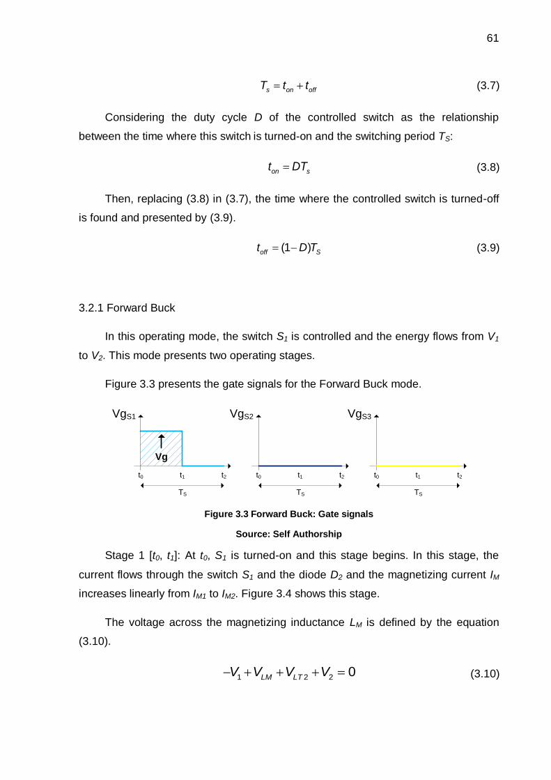
61
s on offT t t (3.7)
Considering the duty cycle D of the controlled switch as the relationship
between the time where this switch is turned-on and the switching period TS:
on st DT (3.8)
Then, replacing (3.8) in (3.7), the time where the controlled switch is turned-off
is found and presented by (3.9).
(1 )off St D T (3.9)
3.2.1 Forward Buck
In this operating mode, the switch S1 is controlled and the energy flows from V1
to V2. This mode presents two operating stages.
Figure 3.3 presents the gate signals for the Forward Buck mode.
VgS2
t0 t1 t2
VgS1
t0 t1 t2
TSTS
VgS3
t0 t1 t2
TS
Vg
Figure 3.3 Forward Buck: Gate signals
Source: Self Authorship
Stage 1 [t0, t1]: At t0, S1 is turned-on and this stage begins. In this stage, the
current flows through the switch S1 and the diode D2 and the magnetizing current IM
increases linearly from IM1 to IM2. Figure 3.4 shows this stage.
The voltage across the magnetizing inductance LM is defined by the equation
(3.10).
1 2 2 0LM LTV V V V (3.10)
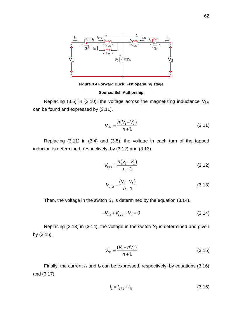
62
+
V1 V2
+
S3
S1 S2
D3
D2
+
+
+ + -
+
- -
-
-
- +
LM
VLT1 VLT2
- -
IM
I1 I2D1
: 1nILT1 ILT2
Figure 3.4 Forward Buck: Fist operating stage
Source: Self Authorship
Replacing (3.5) in (3.10), the voltage across the magnetizing inductance VLM
can be found and expressed by (3.11).
1 2
1LM
n V VV
n (3.11)
Replacing (3.11) in (3.4) and (3.5), the voltage in each turn of the tapped
inductor is determined, respectively, by (3.12) and (3.13).
1 2
11
LT
n V VV
n (3.12)
1 2
21
LT
V VV
n (3.13)
Then, the voltage in the switch S3 is determined by the equation (3.14).
3 2 2 0S LTV V V (3.14)
Replacing (3.13) in (3.14), the voltage in the switch S3 is determined and given
by (3.15).
1 2
31
S
V nVV
n (3.15)
Finally, the current I1 and I2 can be expressed, respectively, by equations (3.16)
and (3.17).
1 1LT MI I I (3.16)

63
2 2LTI I (3.17)
For this stage, the relationship between I1 and I2 can be expressed by (3.18).
1 2I I (3.18)
Replacing (3.6) in (3.17) and considering the relationship in (3.18), the current
ILT1 can be rewritten as (3.19).
11LT
II
n (3.19)
Replacing (3.19) in (3.16) and considering the relationship in (3.18), the current
I1 and I2 are determined, respectively, by (3.20) and (3.21).
11
MnII
n (3.20)
21MnI
In
(3.21)
Stage 2 [t1, t2]: At t1, S1 is turned-off and this stage begins. When S1 in turned-
off at t1, the current finds a path through the diodes D3 and D2 and the magnetizing
current IM decreases linearly from IM2 to IM1. Figure 3.5 shows this stage.
V1 V2
+ +
S3
S1 S2
D3
D2
+
+
+ + -
+
- -
-
-
- +
LM
VLT1 VLT2
- -
IM
I1 I2D1
: 1nILT1 ILT2
Figure 3.5 Forward Buck: Second operating stage
Source: Self Authorship
For this mode, the voltage VLT2 across the secondary of the tapped inductor is
determined by the equation (3.22).
2 2LTV V (3.22)

64
Replacing (3.22) in (3.3) it is possible to find the voltage VLT1 in the primary of
the tapped inductor. Equation (3.23) expresses that.
1 2LTV nV (3.23)
As mentioned before, VLM and VLT1 are in parallel and have the same voltage,
then:
2LMV nV (3.24)
The voltage across the switch S1 can be expressed by (3.25).
1 1 1 0S LTV V V (3.25)
Replacing (3.23) in (3.25), the voltage in the switch S1 is represented by (3.26).
1 1 2SV V nV (3.26)
In this stage, as the switch S1 is off, there is no current I1:
1 0I (3.27)
Then, replacing (3.27) in (3.16), the current in the primary of tapped inductor is
determined and given by (3.28).
1LT MI I (3.28)
Substituting (3.28) into (3.6) and considering (3.17), the current I2 can be
expressed by (3.29).
2 MI nI (3.29)
Analyzed the two stages, the theoretical waveforms for the Forward Buck mode
can be drawn. Figure 3.6 presents the voltage in the switches.

65
VS3
t0 t1 t2
VS1
t0 t1 t2
V1+nV2V1+nV2
n+1
TS TS
Figure 3.6 Forward Buck: Theoretical voltage waveforms in the switches S1 and S3
Source: Self Authorship
Figure 3.7 presents the voltage in the tapped inductor.
VLT2VLT1
n(V1-V2)n+1
(V1-V2)n+1
t0 t1 t2t0 t1 t2
-nV2 -V2
TSTS
Figure 3.7 Forward Buck: Theoretical voltage waveforms in the tapped inductor
Source: Self Authorship
Figure 3.8 presents the theoretical waveforms of the voltage VLM and the
magnetizing current IM in the magnetizing inductance LM.
IM
t0 t1 t2
TS
VLM
n(V1-V2)n+1
t0 t1 t2
-nV2
TS
IM2
IM1
Figure 3.8 Forward Buck: Theoretical waveforms in the magnetizing inductance
Source: Self Authorship
Then, figure 3.9 shows the waveforms of the current I1 and the current I2.
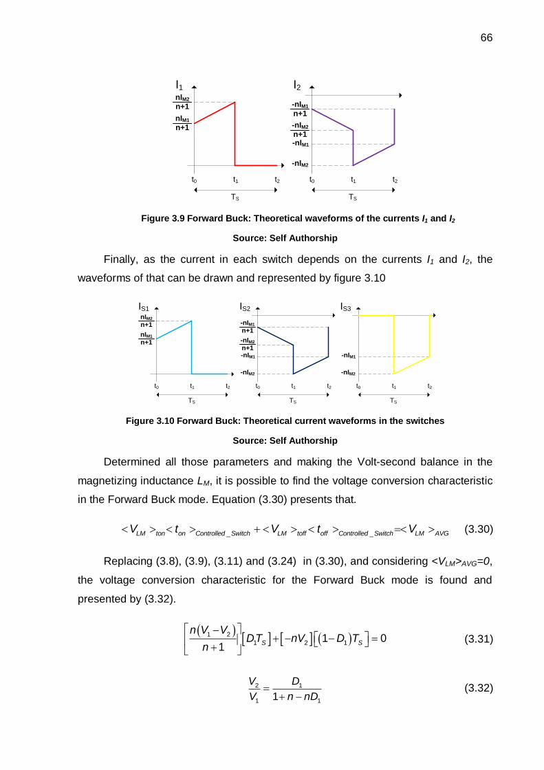
66
I1
t0 t1 t2
TS
nIM1
n+1
nIM2
n+1
I2
t0 t1 t2
TS
-nIM2
n+1
-nIM1
n+1
-nIM1
-nIM2
Figure 3.9 Forward Buck: Theoretical waveforms of the currents I1 and I2
Source: Self Authorship
Finally, as the current in each switch depends on the currents I1 and I2, the
waveforms of that can be drawn and represented by figure 3.10
IS1
t0 t1 t2
TS
nIM1
n+1
nIM2
n+1
IS2
t0 t1 t2
TS
-nIM2
n+1
-nIM1
n+1
-nIM1
-nIM2
IS3
t0 t1 t2
TS
-nIM1
-nIM2
Figure 3.10 Forward Buck: Theoretical current waveforms in the switches
Source: Self Authorship
Determined all those parameters and making the Volt-second balance in the
magnetizing inductance LM, it is possible to find the voltage conversion characteristic
in the Forward Buck mode. Equation (3.30) presents that.
_ _LM ton on Controlled Switch LM toff off Controlled Switch LM AVGV t V t V (3.30)
Replacing (3.8), (3.9), (3.11) and (3.24) in (3.30), and considering <VLM>AVG=0,
the voltage conversion characteristic for the Forward Buck mode is found and
presented by (3.32).
1 2
1 2 11 01
S S
n V VDT nV D T
n (3.31)
2 1
1 11
V D
V n nD (3.32)
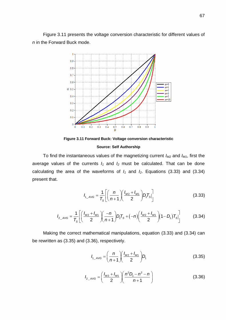
67
Figure 3.11 presents the voltage conversion characteristic for different values of
n in the Forward Buck mode.
Figure 3.11 Forward Buck: Voltage conversion characteristic
Source: Self Authorship
To find the instantaneous values of the magnetizing current IM2 and IM1, first the
average values of the currents I1 and I2 must be calculated. That can be done
calculating the area of the waveforms of I1 and I2. Equations (3.33) and (3.34)
present that.
2 11_ 1
1
1 2M M
AVG S
S
I InI DT
T n (3.33)
2 1 2 12 _ 1 1
11
2 1 2M M M M
AVG S S
S
I I I InI DT n D T
T n (3.34)
Making the correct mathematical manipulations, equation (3.33) and (3.34) can
be rewritten as (3.35) and (3.36), respectively.
2 11_ 1
1 2M M
AVG
I InI D
n (3.35)
2 2
2 1 12 _
2 1M M
AVG
I I n D n nI
n (3.36)

68
Considering equation (3.37) and analyzing the magnetizing inductance in the
first stage, it is possible to find the first relationship between IM1 and IM2. This
relationship is presented by (3.38).
MLM M
IV L
t (3.37)
1 2 1
2 11
M M
S M
n V V DI I
f L n (3.38)
Considering the ideal converter, the power processed PC by the converter must
be the same in the voltage source V1 and V2. This can be expressed by the equation
(3.39).
1 2C V VP P P (3.39)
Then, the power PV1 in the source V1 can be represented by (3.40).
1 1 1_V AVGP VI (3.40)
Replacing (3.35) and (3.39) in (3.40), and making the correct mathematical
manipulations, the second relationship between IM1 and IM2 can be found. This
relation is presented by (3.41).
2 1
1 1
2 1C
M M
P nI I
V D n (3.41)
Now, summing equations (3.38) and (3.41) the value of the magnetizing current
IM2 is found and given by equation (3.42).
2 2 2
1 1 1 2
2
1 1
2 1
2 1
C S M
M
S M
P f L n V D n V VI
V D f L n n (3.42)
Then, replacing (3.42) in (3.41), IM1 can be found and determined by (3.43).
2 2 2
1 1 1 2
1
1 1
2 1
2 1
C S M
M
S M
P f L n V D n V VI
V D f L n n (3.43)

69
Specified the values of IM1 and IM2, the RMS value of the current in the
semiconductors can be calculated. Equation (3.44) represents the RMS current for
the switch S1.
2
1_ 1
0
1( )
ST
S RMS S
S
I I t dtT
(3.44)
Considering the function of IS1(t) given by (3.45).
2 11 1
1 1
1
, 0( ) 1 1
0,
M MM S
S S
S S
I In nt I t DT
I t n D T n
DT t T
(3.45)
Then, replacing (3.45) in (3.44), equation (3.44) can be rewritten as (3.46).
1
1
2
22 11_ 1
10
10
1 1
S S
S
D T T
M MS RMS M
S S D T
I In nI t I dt dt
T n DT n (3.46)
Replacing (3.42) and (3.43) in (3.46) and solving the equation, IS1_RMS is found
and given by (3.47).
24 2 4
1 1 1 2
1_ 2 42 2 211
1 1
32 1 12 1S RMS
M s M C S
D V n V VI
DV L f n L P f n (3.47)
The same procedure can be applied to switches S2 and S3. Equation (3.48)
expresses the RMS current for the switch S2.
2
2 _ 2
0
1( )
ST
S RMS S
S
I I t dtT
(3.48)
Considering the function of IS2(t) given by (3.49).
2 11 1
1
2
2 1 1 1 2 1
1 1
, 01 1
( )
,1 1
M MM S
S
S
M M M M S S
S
I In nt I t DT
n DT nI t
n nI I t D I I DT t T
D T D
(3.49)

70
Then, replacing (3.49) in (3.48), equation (3.48) can be rewritten as (3.50).
1
1
2
2 11
10
2
2 _ 2 1
1
1 1 2
1
1 1
1
1
1
S
S
S
D T
M MM
S
S RMS M MTS S
D T
M M
I In nt I dt
n DT n
nI I I tT D T
dtn
D I ID
(3.50)
Substituting (3.42) and (3.43) into (3.50), and solving the equation, IS2_RMS is
found and given by (3.51).
2 22 4 4
1 1 1 2 1
62 2 2 6 5 4 3 2
1
2 _ 2
1 1
3 1 2
36 1 6 14 16 9 2
6 1
M C S
S RMS
M S
V D n V V n D n n
L P f n D n n n n n nI
V D L f n (3.51)
Finally, equation (3.52) expresses the RMS current in the switch S3
2
3 _ 3
0
1( )
ST
S RMS S
S
I I t dtT
(3.52)
Considering the function of IS3(t) given by (3.53).
1
3
2 1 1 1 2 1
1 1
0, 0
( ),
1 1
S
S
M M M M S S
S
t DT
I t n nI I t D I I DT t T
D T D
(3.53)
This way, replacing (3.53) in (3.52), equation (3.52) can be rewritten as (3.54).
1
1
2
2 12
1
3 _
0
1 1 2
1
110
1
S S
S
M MD T TS
S RMS
S D T
M M
nI I t
D TI dt dt
T nD I I
D
(3.54)

71
Then, replacing (3.42) and (3.43) in (3.54), and solving the equation, IS3_RMS is
found and given by (3.55).
24 2 4
1 1 1 21
3 _ 42 2 21 1
11
2 1 3 12 1S RMS
M sM C S
D V n V VDI
DV L f n L P f n (3.55)
3.2.2 Forward Boost
In this operating mode the switch S3 is controlled whereas the switch S1 is
always turned-on. The energy flows from V1 to V2 and this mode presents two
operating stages.
Figure 3.12 presents the gate signals for the Forward Boost mode.
VgS2
t0 t1 t2
VgS1
t0 t1 t2
TSTS
VgS3
t0 t1 t2
TS
VgVg
Figure 3.12 Forward Boost: Gate signals
Source: Self Authorship
Stage 1 [t0, t1]: At t0, S1 is already on and S3 is turned-on. In this moment this
stage begins. In this stage, the current flows through the switch S1 and the switch S3
and the magnetizing current IM increases linearly from IM1 to IM2. Figure 3.13 shows
this stage.
V1 V2
+ +
S3
S1 S2
D3
D2
+
+
+ + -
+
- -
-
-
- +
LM
VLT1 VLT2
- -
IM
I1 I2D1
: 1nILT1 ILT2
Figure 3.13 Forward Boost: First operating stage
Source: Self Authorship
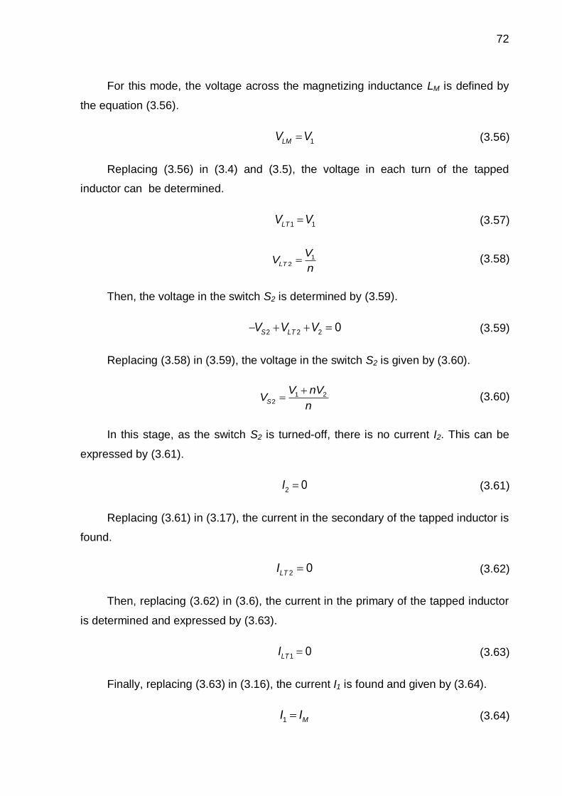
72
For this mode, the voltage across the magnetizing inductance LM is defined by
the equation (3.56).
1LMV V (3.56)
Replacing (3.56) in (3.4) and (3.5), the voltage in each turn of the tapped
inductor can be determined.
1 1LTV V (3.57)
12LT
VV
n (3.58)
Then, the voltage in the switch S2 is determined by (3.59).
2 2 2 0S LTV V V (3.59)
Replacing (3.58) in (3.59), the voltage in the switch S2 is given by (3.60).
1 22S
V nVV
n (3.60)
In this stage, as the switch S2 is turned-off, there is no current I2. This can be
expressed by (3.61).
2 0I (3.61)
Replacing (3.61) in (3.17), the current in the secondary of the tapped inductor is
found.
2 0LTI (3.62)
Then, replacing (3.62) in (3.6), the current in the primary of the tapped inductor
is determined and expressed by (3.63).
1 0LTI (3.63)
Finally, replacing (3.63) in (3.16), the current I1 is found and given by (3.64).
1 MI I (3.64)
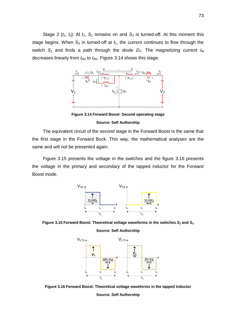
73
Stage 2 [t1, t2]: At t1, S1 remains on and S3 is turned-off. At this moment this
stage begins. When S3 in turned-off at t1, the current continues to flow through the
switch S1 and finds a path through the diode D2. The magnetizing current IM
decreases linearly from IM2 to IM1. Figure 3.14 shows this stage.
V1 V2
+ +
S3
S1 S2
D3
D2
+
+
+ + -
+
- -
-
-
- +
LM
VLT1 VLT2
- -
IM
I1 I2D1
: 1nILT1 ILT2
Figure 3.14 Forward Boost: Second operating stage
Source: Self Authorship
The equivalent circuit of the second stage in the Forward Boost is the same that
the first stage in the Forward Buck. This way, the mathematical analyses are the
same and will not be presented again.
Figure 3.15 presents the voltage in the switches and the figure 3.16 presents
the voltage in the primary and secondary of the tapped inductor for the Forward
Boost mode.
VS3
t0 t1 t2
V1+nV2
n+1
VS2
t0 t1 t2
V1+nV2
n
TSTS
Figure 3.15 Forward Boost: Theoretical voltage waveforms in the switches S2 and S3
Source: Self Authorship
VLT2VLT1
n(V1-V2)n+1
(V1-V2)n+1
t0 t1 t2
V1 nV1
t0 t1 t2
TSTS
Figure 3.16 Forward Boost: Theoretical voltage waveforms in the tapped inductor
Source: Self Authorship

74
Figure 3.17 presents the theoretical waveforms of the voltage VLM and the
magnetizing current IM in the magnetizing inductance LM.
t0 t1 t2
TS
IM
t0 t1 t2
TS
VLM
IM2
IM1
n(V1-V2)n+1
V1
Figure 3.17 Forward Boost: Theoretical waveforms in the magnetizing inductance
Source: Self Authorship
Figure 3.18 shows the waveforms of the currents I1 and I2.
I1
t0 t1 t2
TS
nIM1
n+1
nIM2
n+1
I2
t0 t1 t2
TS
-nIM2
n+1
-nIM1
n+1
IM2
IM1
Figure 3.18 Forward Boost: Theoretical waveforms of the currents I1 and I2
Source: Self Authorship
Figure 3.19 presents the current in the switches for the Forward Boost mode.
IS1
t0 t1 t2
TS
nIM1
n+1
nIM2
n+1
IS2
t0 t1 t2
TS
-nIM2
n+1
-nIM1
n+1
IM2
IM1
IS3
t0 t1 t2
TS
IM2
IM1
Figure 3.19 Forward Boost: Theoretical current waveforms in the switches
Source: Self Authorship
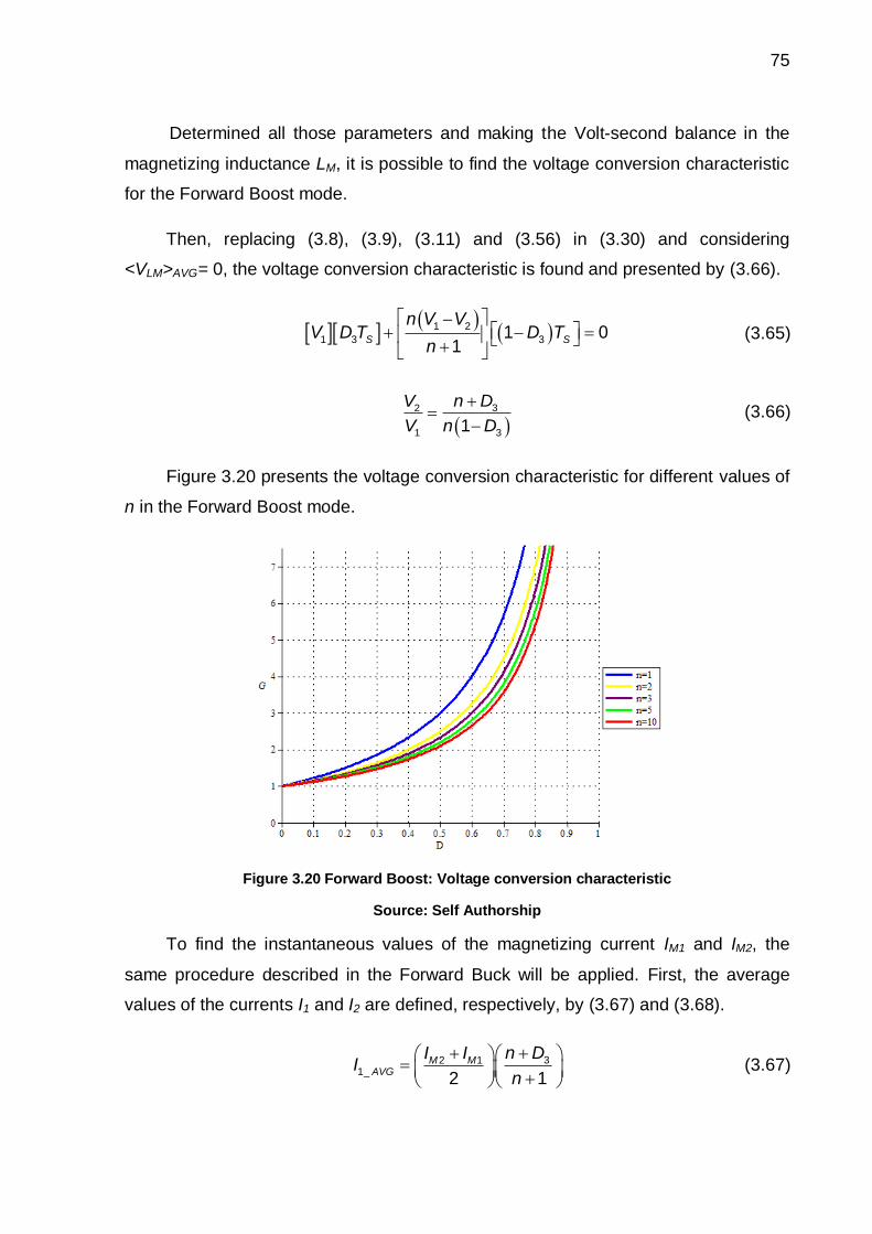
75
Determined all those parameters and making the Volt-second balance in the
magnetizing inductance LM, it is possible to find the voltage conversion characteristic
for the Forward Boost mode.
Then, replacing (3.8), (3.9), (3.11) and (3.56) in (3.30) and considering
<VLM>AVG= 0, the voltage conversion characteristic is found and presented by (3.66).
1 2
1 3 31 01
S S
n V VV D T D T
n (3.65)
32
1 31
n DV
V n D (3.66)
Figure 3.20 presents the voltage conversion characteristic for different values of
n in the Forward Boost mode.
Figure 3.20 Forward Boost: Voltage conversion characteristic
Source: Self Authorship
To find the instantaneous values of the magnetizing current IM1 and IM2, the
same procedure described in the Forward Buck will be applied. First, the average
values of the currents I1 and I2 are defined, respectively, by (3.67) and (3.68).
32 11_
2 1M M
AVG
n DI II
n (3.67)
76
2 12 _ 31
2 1M M
AVG
I I nI D
n (3.68)
Then, analyzing the magnetizing inductance LM, the first relationship between
IM1 and IM2 is found and represented by (3.69).
1 32 1M M
S M
V DI I
f L (3.69)
Making the power balance in the voltage source V1, the second relationship
between IM1 and IM2 is found and presented by (3.70).
2 1
1 3
2 1C
M M
P nI I
V n D (3.70)
Summing equations (3.69) and (3.70), the instantaneous value of the
magnetizing current IM2 can be defined by (3.71).
2
1 3 3
2
1 3
2 1
2
C S M
M
S M
P f L n V D n DI
V f L n D (3.71)
Then, replacing (3.71) in (3.70), the instantaneous value of the magnetizing
current IM1 can be represented by (3.72).
2
1 3 3
1
1 3
2 1
2
C S M
M
S M
P f L n V D n DI
V f L n D (3.72)
Defined the values of IM1 and IM2, the RMS current in the semiconductors can be
calculated.
Considering the function of IS1(t) given by (3.73).
2 11 3
3
1
2 1 32 13
3 3
, 0
( )
,1 1 1 1
M MM S
S
S
M MM MS S
S
I It I t D T
D TI t
I I DI In nt D T t T
n D T n D
(3.73)
Replacing (3.73) in (3.44), equation (3.44) can be rewritten as (3.74).
77
3
3
2
2 11
30
1_ 2
2 1 32 1
3 3
1
1 1 1 1
S
S
S
D T
M MM
S
S RMST
SM MM M
SD T
I It I dt
D TI
TI I DI In n
t dtn D T n D
(3.74)
Replacing (3.71) and (3.72) in (3.74), and solving the equation, IS1_RMS is found
and given by (3.75).
4 2 3 2 2 3 4 3 2 2
1 3 3 3 3 3
2 2 2 3 4 2 3 2
3 3 3 3
1_
1 3
3 2 5 4 2
36 2 5 2 4
6 1
M C S
S RMS
M S
V D D n D n D n n D D n Dn
L P f D n n D n n D n n DI
V L f D n n (3.75)
Now, considering the function of IS2(t) given by (3.76):
3
2 2 1 32 13
3 3
0, 0
( ),
1 1 1 1
S
S M MM MS S
S
t D T
I t I I DI In nt D T t T
n D T n D
(3.76)
Replacing (3.76) in (3.48), equation (3.48) can be rewritten as (3.77).
3
3
2
2 12
3
2 _
0 2 1 3
3
1 110
1 1
S S
S
M M
D T TS
S RMS
S D T M M
I Int
n D TI dt dt
T I I Dn
n D
(3.77)
Substituting (3.71) and (3.72) into (3.77), and solving the equation, IS2_RMS is
found and given by (3.78).
22 4
3 1 3
2 _ 3 22 2 21 3
3 16 1 12 1
S RMS
M sM C S
D V n DnI D
V L f n n D L P f n (3.78)
Finally, considering the function of IS3(t) given by (3.79):
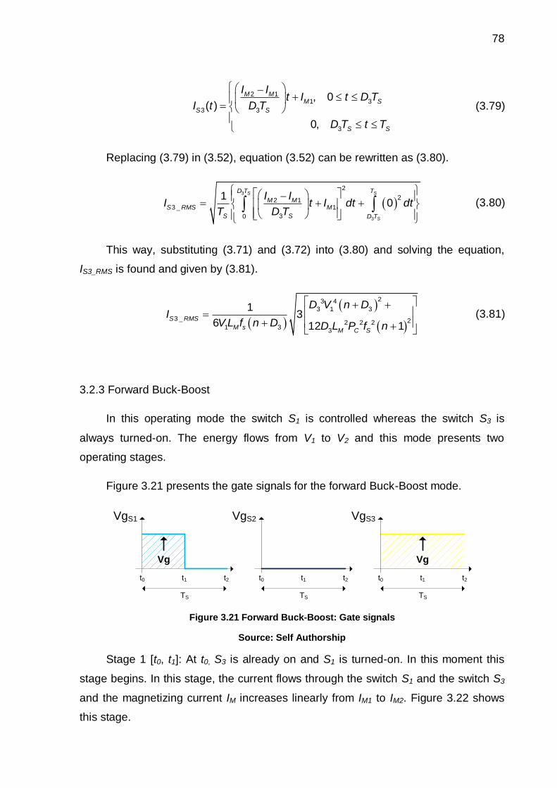
78
2 11 3
3 3
3
, 0( )
0,
M MM S
S S
S S
I It I t D T
I t D T
D T t T
(3.79)
Replacing (3.79) in (3.52), equation (3.52) can be rewritten as (3.80).
3
3
2
22 13 _ 1
30
10
S S
S
D T T
M MS RMS M
S S D T
I II t I dt dt
T D T (3.80)
This way, substituting (3.71) and (3.72) into (3.80) and solving the equation,
IS3_RMS is found and given by (3.81).
23 4
3 1 3
3 _ 22 2 21 3
3
13
6 12 1S RMS
M sM C S
D V n DI
V L f n D D L P f n (3.81)
3.2.3 Forward Buck-Boost
In this operating mode the switch S1 is controlled whereas the switch S3 is
always turned-on. The energy flows from V1 to V2 and this mode presents two
operating stages.
Figure 3.21 presents the gate signals for the forward Buck-Boost mode.
TSTS TS
Vg
VgS2
t0 t1 t2
VgS1
t0 t1 t2
VgS3
t0 t1 t2
Vg
Figure 3.21 Forward Buck-Boost: Gate signals
Source: Self Authorship
Stage 1 [t0, t1]: At t0, S3 is already on and S1 is turned-on. In this moment this
stage begins. In this stage, the current flows through the switch S1 and the switch S3
and the magnetizing current IM increases linearly from IM1 to IM2. Figure 3.22 shows
this stage.

79
V1 V2
+ +
S3
S1 S2
D3
D2
+
+
+ + -
+
- -
-
-
- +
LM
VLT1 VLT2
- -
IM
I1 I2D1
: 1nILT1 ILT2
Figure 3.22 Forward Buck-Boost: First operating stage
Source: Self Authorship
The equivalent circuit of the first stage in the Forward Buck-Boost is the same
that the first stage in the Forward Boost. Then, the mathematical analyses are the
same and will not be presented again.
Stage 2 [t1, t2]: At t1, S3 remains on and S1 is turned off. At this moment, this
stage begins. The current continues to flow through the switch S3 and finds a path
through the diode D2. For this stage, the magnetizing current decreases linearly from
IM2 to IM1. Figure 3.23 shows this stage.
V1 V2
+ +
S3
S1 S2
D3
D2
+
+
+ + -
+
- -
-
-
- +
LM
VLT1 VLT2
- -
IM
I1 I2D1
: 1nILT1 ILT2
Figure 3.23 Forward Buck-Boost: Second operating stage
Source: Self Authorship
The equivalent circuit of the second stage in the Forward Buck-Boost is the
same that the second stage in the Forward Buck. Then, the mathematical analyses
are the same and will not be presented again.
Figure 3.24 presents the voltage in the switches and the figure 3.25 presents
the voltage in the primary and secondary of the tapped inductor for the Forward
Buck-Boost mode.
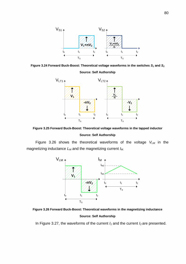
80
VS1
t0 t1 t2
V1+nV2
TS
VS2
t0 t1 t2
V1+nV2
n
TS
Figure 3.24 Forward Buck-Boost: Theoretical voltage waveforms in the switches S1 and S2
Source: Self Authorship
VLT2VLT1
V1
t0 t1 t2t0 t1 t2
V1
TSTS
-nV2 -V2
n
Figure 3.25 Forward Buck-Boost: Theoretical voltage waveforms in the tapped inductor
Source: Self Authorship
Figure 3.26 shows the theoretical waveforms of the voltage VLM in the
magnetizing inductance LM and the magnetizing current IM.
t0 t1 t2
TS
IM
t0 t1 t2
TS
VLM
IM2
IM1V1
-nV2
Figure 3.26 Forward Buck-Boost: Theoretical waveforms in the magnetizing inductance
Source: Self Authorship
In Figure 3.27, the waveforms of the current I1 and the current I2 are presented.
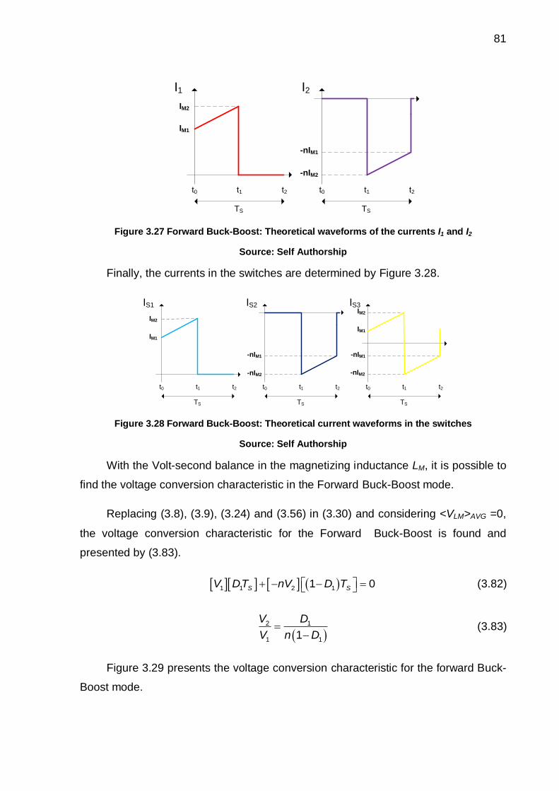
81
I1
t0 t1 t2
TS
I2
t0 t1 t2
TS
-nIM2
-nIM1
IM2
IM1
Figure 3.27 Forward Buck-Boost: Theoretical waveforms of the currents I1 and I2
Source: Self Authorship
Finally, the currents in the switches are determined by Figure 3.28.
IS1
t0 t1 t2
TS
IS2
t0 t1 t2
TS
-nIM2
-nIM1
IM2
IM1
IS3
t0 t1 t2
TS
-nIM1
-nIM2
IM2
IM1
Figure 3.28 Forward Buck-Boost: Theoretical current waveforms in the switches
Source: Self Authorship
With the Volt-second balance in the magnetizing inductance LM, it is possible to
find the voltage conversion characteristic in the Forward Buck-Boost mode.
Replacing (3.8), (3.9), (3.24) and (3.56) in (3.30) and considering <VLM>AVG =0,
the voltage conversion characteristic for the Forward Buck-Boost is found and
presented by (3.83).
1 1 2 11 0S SV DT nV D T (3.82)
2 1
1 11
V D
V n D (3.83)
Figure 3.29 presents the voltage conversion characteristic for the forward Buck-
Boost mode.
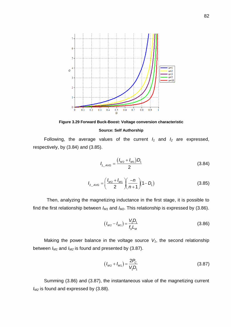
82
Figure 3.29 Forward Buck-Boost: Voltage conversion characteristic
Source: Self Authorship
Following, the average values of the current I1 and I2 are expressed,
respectively, by (3.84) and (3.85).
2 1 1
1_2
M M
AVG
I I DI (3.84)
2 12 _ 11
2 1M M
AVG
I I nI D
n (3.85)
Then, analyzing the magnetizing inductance in the first stage, it is possible to
find the first relationship between IM1 and IM2. This relationship is expressed by (3.86).
1 12 1M M
S M
V DI I
f L (3.86)
Making the power balance in the voltage source V1, the second relationship
between IM1 and IM2 is found and presented by (3.87).
2 1
1 1
2 CM M
PI I
V D (3.87)
Summing (3.86) and (3.87), the instantaneous value of the magnetizing current
IM2 is found and expressed by (3.88).

83
2 2
1 12
1 1
2
2C S M
M
S M
P f L V DI
V D f L (3.88)
Replacing (3.88) in (3.87), the instantaneous value of the magnetizing current
IM1 is determined by (3.89).
2 2
1 11
1 1
2
2C S M
M
S M
P f L V DI
V D f L (3.89)
Defined the values of IM1 and IM2, the RMS current in the semiconductors can be
calculated.
Considering the function of IS1(t) given by (3.90):
2 11 1
1 1
1
, 0( )
0,
M MM S
S S
S S
I It I t DT
I t DT
DT t T
(3.90)
Replacing (3.90) in (3.44), equation (3.44) can be rewritten as (3.91).
1
1
2
22 11_ 1
10
10
S S
S
D T T
M MS RMS M
S S D T
I II t I dt dt
T DT (3.91)
Substituting (3.88) and (3.89) into (3.91), and solving the equation, IS1_RMS is
found and determined by (3.92).
4 4 2 2 2
1 11_
1 1
1213
6M C S
S RMS
M s
D V L P fI
V L f D (3.92)
Then, considering the function of IS2(t) given by (3.93).
1
2 2 1 12 11
1 1
0, 0
( ),
1 1
S
S M MM MS S
S
t DT
I t I I DI In t n DT t T
D T D
(3.93)
Replacing (3.93) in (3.48), equation (3.48) can be rewritten as (3.94).
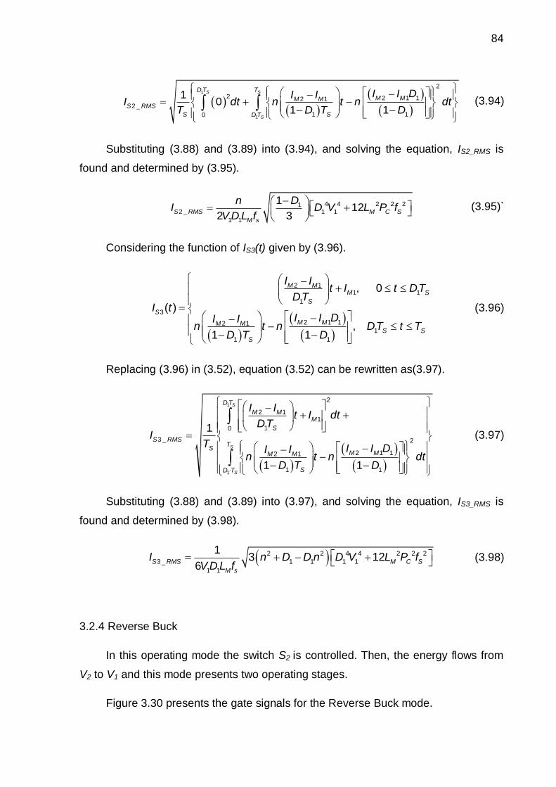
84
1
1
2
2 2 1 12 12 _
1 10
10
1 1
S S
S
D T T
M MM MS RMS
S SD T
I I DI II dt n t n dt
T D T D (3.94)
Substituting (3.88) and (3.89) into (3.94), and solving the equation, IS2_RMS is
found and determined by (3.95).
4 4 2 2 212 _ 1 1
1 1
112
2 3S RMS M C S
M s
DnI D V L P f
V D L f (3.95)`
Considering the function of IS3(t) given by (3.96).
2 11 1
1
3
2 1 12 11
1 1
, 0
( )
,1 1
M MM S
S
S
M MM MS S
S
I It I t DT
DTI t
I I DI In t n DT t T
D T D
(3.96)
Replacing (3.96) in (3.52), equation (3.52) can be rewritten as(3.97).
1
1
2
2 11
10
3 _ 2
2 1 12 1
1 1
1
1 1
S
S
S
D T
M MM
S
S RMST
SM MM M
SD T
I It I dt
DTI
T I I DI In t n dt
D T D
(3.97)
Substituting (3.88) and (3.89) into (3.97), and solving the equation, IS3_RMS is
found and determined by (3.98).
2 2 4 4 2 2 2
3 _ 1 1 1 1
1 1
13 12
6S RMS M C S
M s
I n D D n D V L P fV D L f
(3.98)
3.2.4 Reverse Buck
In this operating mode the switch S2 is controlled. Then, the energy flows from
V2 to V1 and this mode presents two operating stages.
Figure 3.30 presents the gate signals for the Reverse Buck mode.
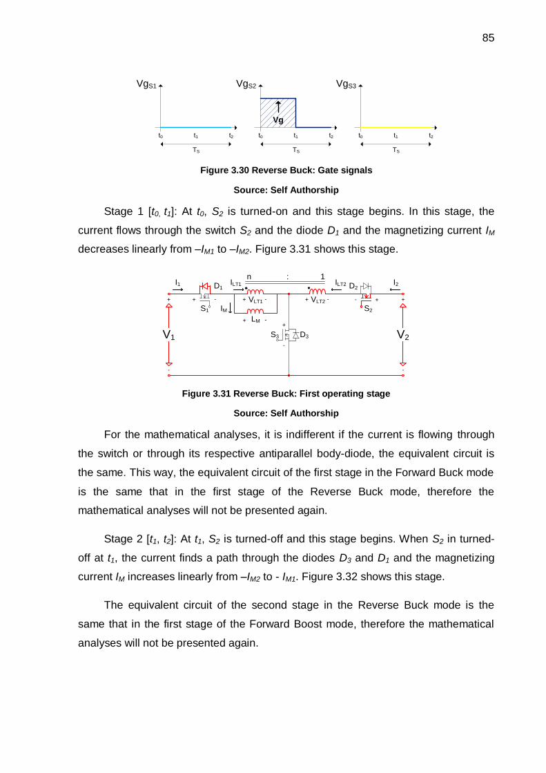
85
VgS2
t0 t1 t2
VgS1
t0 t1 t2
TSTS
VgS3
t0 t1 t2
TS
Vg
Figure 3.30 Reverse Buck: Gate signals
Source: Self Authorship
Stage 1 [t0, t1]: At t0, S2 is turned-on and this stage begins. In this stage, the
current flows through the switch S2 and the diode D1 and the magnetizing current IM
decreases linearly from –IM1 to –IM2. Figure 3.31 shows this stage.
V1 V2
+ +
S3
S1 S2
D3
D2
+
+
+ + -
+
- -
-
-
- +
LM
VLT1 VLT2
- -
IM
I1 I2D1
: 1nILT1 ILT2
Figure 3.31 Reverse Buck: First operating stage
Source: Self Authorship
For the mathematical analyses, it is indifferent if the current is flowing through
the switch or through its respective antiparallel body-diode, the equivalent circuit is
the same. This way, the equivalent circuit of the first stage in the Forward Buck mode
is the same that in the first stage of the Reverse Buck mode, therefore the
mathematical analyses will not be presented again.
Stage 2 [t1, t2]: At t1, S2 is turned-off and this stage begins. When S2 in turned-
off at t1, the current finds a path through the diodes D3 and D1 and the magnetizing
current IM increases linearly from –IM2 to - IM1. Figure 3.32 shows this stage.
The equivalent circuit of the second stage in the Reverse Buck mode is the
same that in the first stage of the Forward Boost mode, therefore the mathematical
analyses will not be presented again.

86
V1 V2
+ +
S3
S1 S2
D3
D2
+
+
+ + -
+
- -
-
-
- +
LM
VLT1 VLT2
- -
IM
I1 I2D1
: 1nILT1 ILT2
Figure 3.32 Reverse Buck: Second operating stage
Source: Self Authorship
Figure 3.33 presents the voltage in the switches and Figure 3.34 presents the
voltage in the primary and secondary of the tapped inductor for the Reverse Buck
mode.
VS3
t0 t1 t2
V1+nV2
n+1
VS2
t0 t1 t2
V1+nV2
n
TSTS
Figure 3.33 Reverse Buck: Theoretical voltage waveforms in the switches S2 and S3
Source: Self Authorship
VLT2VLT1
n(V1-V2)n+1
(V1-V2)n+1
t0 t1 t2t0 t1 t2
V1 nV1
TSTS
Figure 3.34 Reverse Buck: Theoretical voltage waveforms in the tapped inductor
Source: Self Authorship
Figure 3.35 shows the theoretical waveforms of the voltage VLM in the
magnetizing inductance LM and the magnetizing current IM for the Reverse Buck
mode.
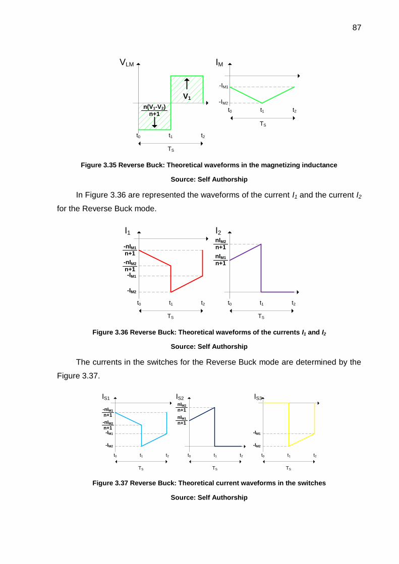
87
VLM
n(V1-V2)n+1
t0 t1 t2
V1
TS
IM
t0 t1 t2
-IM2
-IM1
TS
Figure 3.35 Reverse Buck: Theoretical waveforms in the magnetizing inductance
Source: Self Authorship
In Figure 3.36 are represented the waveforms of the current I1 and the current I2
for the Reverse Buck mode.
I1
t0 t1 t2
TS
-nIM2
n+1
-nIM1
n+1
-IM1
-IM2
I2
t0 t1 t2
TS
nIM1
n+1
nIM2
n+1
Figure 3.36 Reverse Buck: Theoretical waveforms of the currents I1 and I2
Source: Self Authorship
The currents in the switches for the Reverse Buck mode are determined by the
Figure 3.37.
TS
IS2
t0 t1 t2
nIM1
n+1
nIM2
n+1
TS
IS1
t0 t1 t2
-nIM2
n+1
-nIM1
n+1
-IM1
-IM2
IS3
TS
t0 t1 t2
-IM1
-IM2
Figure 3.37 Reverse Buck: Theoretical current waveforms in the switches
Source: Self Authorship
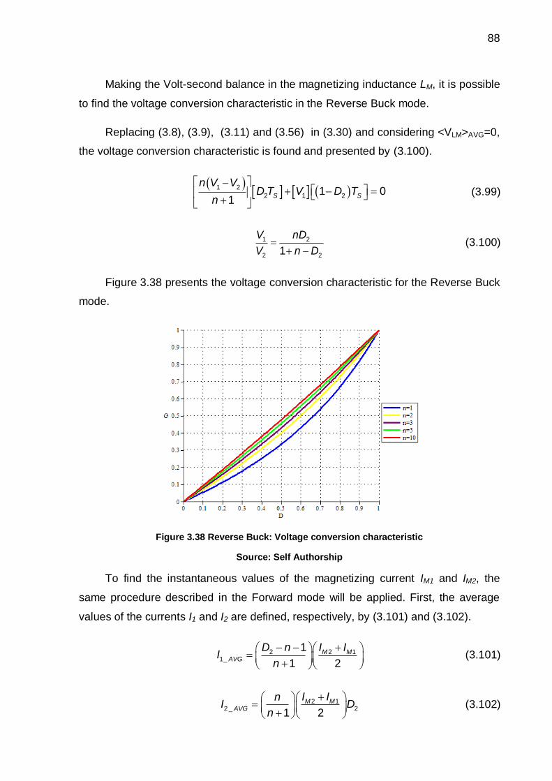
88
Making the Volt-second balance in the magnetizing inductance LM, it is possible
to find the voltage conversion characteristic in the Reverse Buck mode.
Replacing (3.8), (3.9), (3.11) and (3.56) in (3.30) and considering <VLM>AVG=0,
the voltage conversion characteristic is found and presented by (3.100).
1 2
2 1 21 01
S S
n V VD T V D T
n (3.99)
1 2
2 21
V nD
V n D (3.100)
Figure 3.38 presents the voltage conversion characteristic for the Reverse Buck
mode.
Figure 3.38 Reverse Buck: Voltage conversion characteristic
Source: Self Authorship
To find the instantaneous values of the magnetizing current IM1 and IM2, the
same procedure described in the Forward mode will be applied. First, the average
values of the currents I1 and I2 are defined, respectively, by (3.101) and (3.102).
2 2 11_
1
1 2M M
AVG
D n I II
n (3.101)
2 12 _ 2
1 2M M
AVG
I InI D
n (3.102)

89
Analyzing the magnetizing inductance in the first stage, it is possible to find the
first relationship between IM1 and IM2. This relationship is expressed by (3.103).
2 1 2
1 21
M M
S M
D n V VI I
f L n (3.103)
To guarantee the correct power balance in the converter, for the Reverse mode
the power PV1 in the voltage source V1 will be considered negative. This can be
expressed by (3.104).
1V CP P (3.104)
This way, making the power balance in the voltage source V1, the second
relationship between IM1 and IM2 is found and presented by (3.105).
1 2
1 2
2 1
1
C
M M
P nI I
V n D (3.105)
Summing (3.103) and (3.105), the instantaneous value of the magnetizing
current IM1 is found and expressed by (3.106).
2
1 2 1 2 2
1
1 2
2 1 1
2 1 1
C S M
M
S M
P n f L nV D V V n DI
V f L n D n (3.106)
Then, replacing (3.106) in (3.105), the instantaneous value of the magnetizing
current IM2 is determined by (3.107).
2
1 2 1 2 2
2
1 2
2 1 1
2 1 1
C S M
M
S M
P n f L nV D V V n DI
V f L n D n (3.107)
Defined the values of IM1 and IM2, the RMS current in the semiconductors can be
calculated.
Considering the function of IS1(t) given by (3.108):
2 11 2
2
1
1 2 22 12
2 2
, 01 1
( )
,1 1
M MM S
S
S
M MM MS S
S
I I n nt I t D T
D T n nI t
I D II It D T t T
D T D
(3.108)
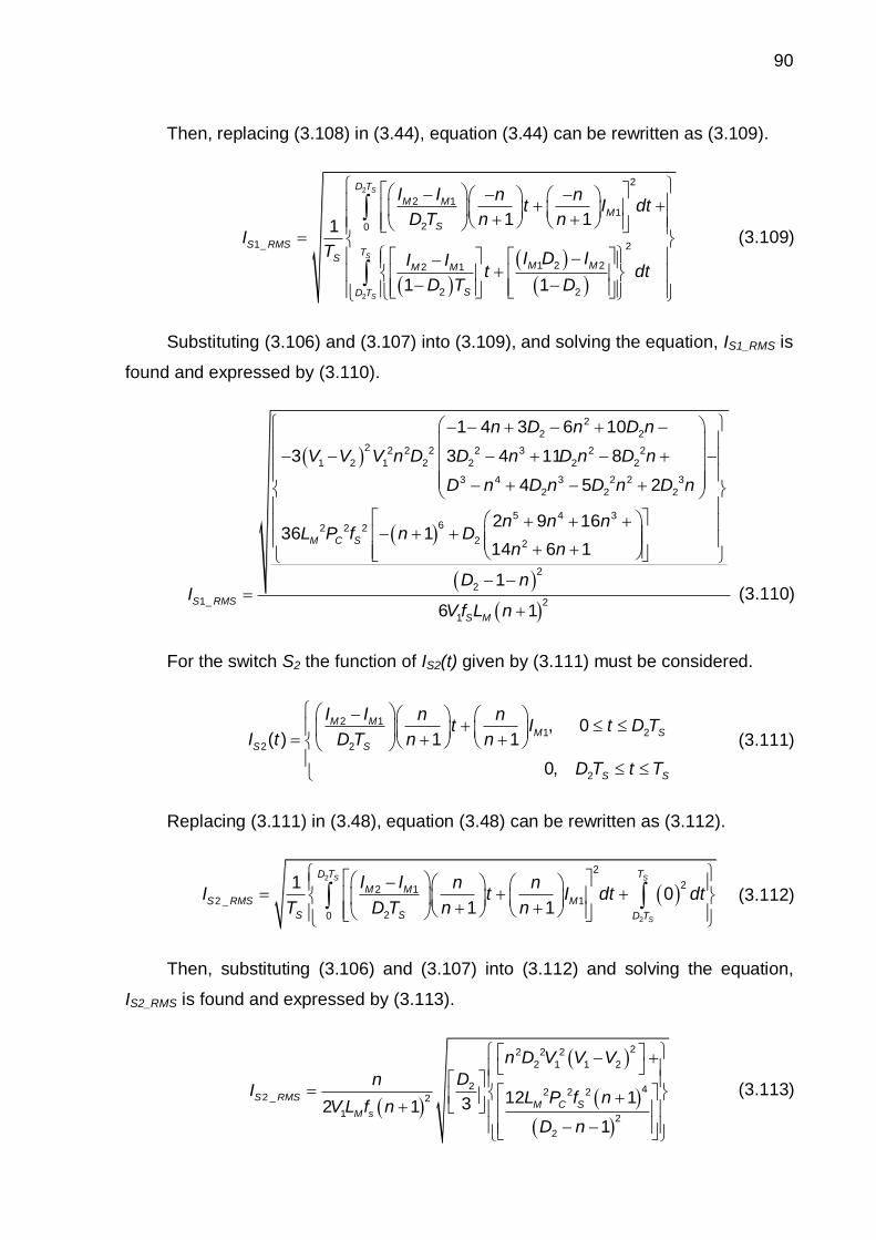
90
Then, replacing (3.108) in (3.44), equation (3.44) can be rewritten as (3.109).
2
2
2
2 11
20
1_ 2
1 2 22 1
2 2
1 11
1 1
S
S
S
D T
M MM
S
S RMST
SM MM M
SD T
I I n nt I dt
D T n nI
T I D II It dt
D T D
(3.109)
Substituting (3.106) and (3.107) into (3.109), and solving the equation, IS1_RMS is
found and expressed by (3.110).
2
2 2
2 2 2 2 2 3 2 2
1 2 1 2 2 2 2
3 4 3 2 2 3
2 2 2
5 4 362 2 2
2 2
2
2
1_ 2
1
1 4 3 6 10
3 3 4 11 8
4 5 2
2 9 1636 1
14 6 1
1
6 1
M C S
S RMS
S M
n D n D n
V V V n D D n D n D n
D n D n D n D n
n n nL P f n D
n n
D nI
V f L n (3.110)
For the switch S2 the function of IS2(t) given by (3.111) must be considered.
2 11 2
2 2
2
, 0( ) 1 1
0,
M MM S
S S
S S
I I n nt I t D T
I t D T n n
D T t T
(3.111)
Replacing (3.111) in (3.48), equation (3.48) can be rewritten as (3.112).
2
2
2
22 12 _ 1
20
10
1 1
S S
S
D T T
M MS RMS M
S S D T
I I n nI t I dt dt
T D T n n (3.112)
Then, substituting (3.106) and (3.107) into (3.112) and solving the equation,
IS2_RMS is found and expressed by (3.113).
22 2 2
2 1 1 2
2 42 2 22 _ 2
1 2
2
12 132 11
S RMSM C S
M s
n D V V V
DnI L P f n
V L f nD n
(3.113)
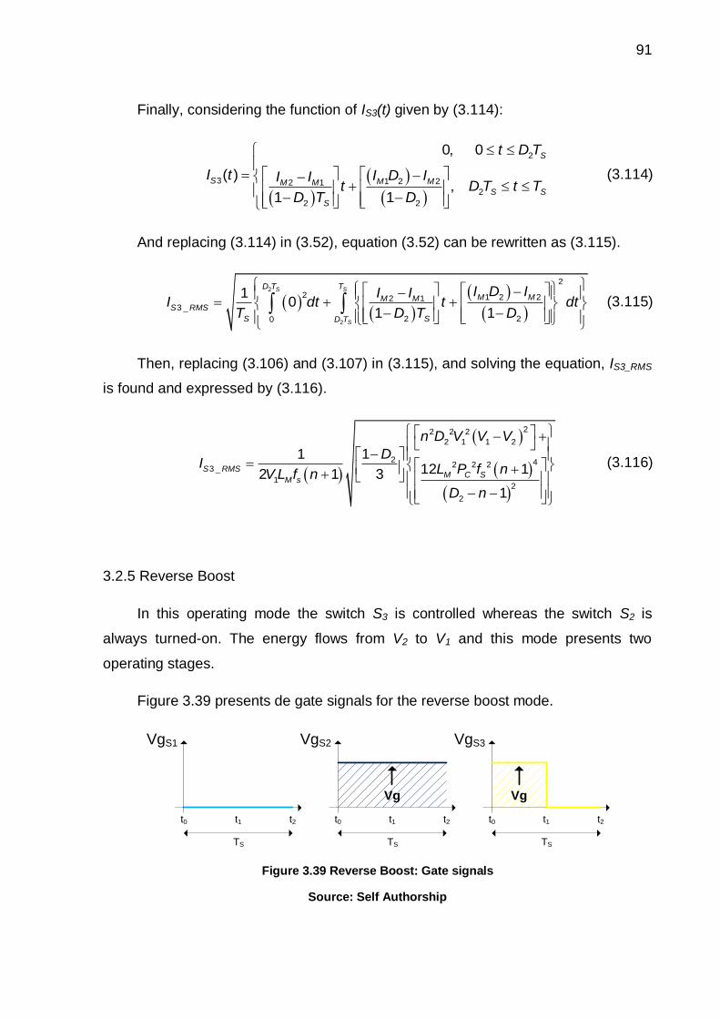
91
Finally, considering the function of IS3(t) given by (3.114):
2
3 1 2 22 12
2 2
0, 0
( ),
1 1
S
S M MM MS S
S
t D T
I t I D II It D T t T
D T D
(3.114)
And replacing (3.114) in (3.52), equation (3.52) can be rewritten as (3.115).
2
2
2
2 1 2 22 13 _
2 20
10
1 1
S S
S
D T T
M MM MS RMS
S SD T
I D II II dt t dt
T D T D (3.115)
Then, replacing (3.106) and (3.107) in (3.115), and solving the equation, IS3_RMS
is found and expressed by (3.116).
22 2 2
2 1 1 2
2 42 2 23 _
12
2
1112 12 1 3
1
S RMSM C S
M s
n D V V V
DI L P f nV L f n
D n
(3.116)
3.2.5 Reverse Boost
In this operating mode the switch S3 is controlled whereas the switch S2 is
always turned-on. The energy flows from V2 to V1 and this mode presents two
operating stages.
Figure 3.39 presents de gate signals for the reverse boost mode.
VgS2
t0 t1 t2
VgS1
t0 t1 t2
TSTS
VgS3
t0 t1 t2
TS
VgVg
Figure 3.39 Reverse Boost: Gate signals
Source: Self Authorship

92
Stage 1 [t0, t1]: At t0, S2 is already on and S3 is turned-on. In this moment this
stage begins. In this stage, the current flows through the switch S2 and the switch S3
and the magnetizing current IM decreases linearly from –IM1 to –IM2. Figure 3.40
shows this stage.
V1 V2
+ +
S3
S1 S2
D3
D2
+
+
+ + -
+
- -
-
-
- +
LM
VLT1 VLT2
- -
IM
I1 I2D1
: 1nILT1 ILT2
Figure 3.40 Reverse Boost: First operating stage
Source: Self Authorship
The equivalent circuit of the first stage in the Reverse Boost mode is the same
that in the second stage of the Forward Buck mode. Then, the mathematical
analyses will not be presented again.
Stage 2 [t1, t2]: At t1, S2 remains on and S3 is turned-off. At this moment this
stage begins. When S3 in turned-off at t1, the current continues to flow through the
switch S2 and finds a path through the diode D1. In this stage, the magnetizing
current IM increases linearly from –IM2 to –IM1. Figure 3.41 shows this stage.
V1 V2
+ +
S3
S1 S2
D3
D2
+
+
+ + -
+
- -
-
-
- +
LM
VLT1 VLT2
- -
IM
I1 I2D1
: 1nILT1 ILT2
Figure 3.41 Reverse Boost: Second operating stage
Source: Self Authorship
The equivalent circuit of the second stage in the Reverse Boost mode is the
same that in the first stage of the Forward Buck mode. Then, the mathematical
analyses will not be presented again.
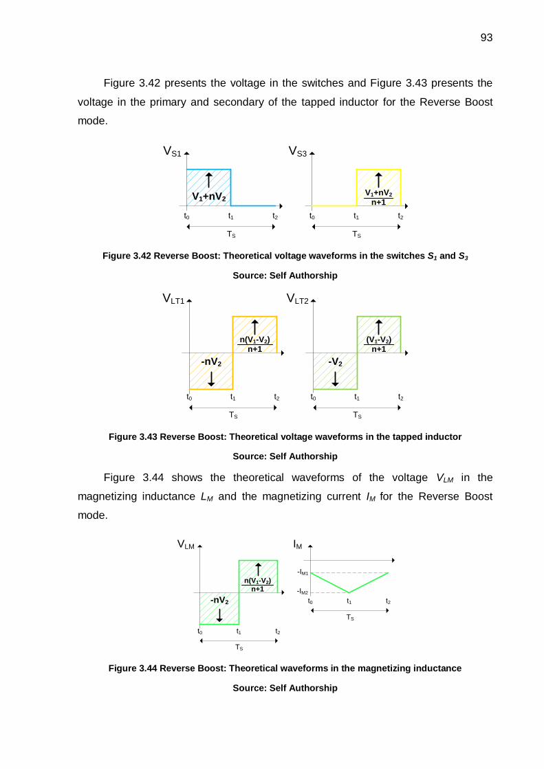
93
Figure 3.42 presents the voltage in the switches and Figure 3.43 presents the
voltage in the primary and secondary of the tapped inductor for the Reverse Boost
mode.
VS1
t0 t1 t2
VS3
t0 t1 t2
TS TS
V1+nV2
n+1V1+nV2
Figure 3.42 Reverse Boost: Theoretical voltage waveforms in the switches S1 and S3
Source: Self Authorship
VLT2VLT1
t0 t1 t2t0 t1 t2
TSTS
(V1-V2)n+1
-nV2 -V2
n(V1-V2)n+1
Figure 3.43 Reverse Boost: Theoretical voltage waveforms in the tapped inductor
Source: Self Authorship
Figure 3.44 shows the theoretical waveforms of the voltage VLM in the
magnetizing inductance LM and the magnetizing current IM for the Reverse Boost
mode.
VLM
t0 t1 t2
TS
IM
t0 t1 t2
-IM2
-IM1
TS
-nV2
n(V1-V2)n+1
Figure 3.44 Reverse Boost: Theoretical waveforms in the magnetizing inductance
Source: Self Authorship

94
In Figure 3.45 the waveforms of the current I1 and the current I2 for the Reverse
Boost mode are represented.
I1
t0 t1 t2
TS
-nIM2
n+1
-nIM1
n+1
I2
t0 t1 t2
TS
nIM1
nIM2
nIM1
n+1
nIM2
n+1
Figure 3.45 Reverse Boost: Theoretical waveforms of the currents I1 and I2
Source: Self Authorship
The currents in the switches for the Reverse Boost mode are determined by
Figure 3.46.
IS1
t0 t1 t2
TS
-nIM2
n+1
-nIM1
n+1
IS2
t0 t1 t2
TS
nIM1
nIM2
nIM1
n+1
nIM2
n+1
TS
t0 t1 t2
IS3
nIM1
nIM2
Figure 3.46 Reverse Boost: Theoretical current waveforms in the switches
Source: Self Authorship
Making the Volt-second balance in the magnetizing inductance LM, it is possible
to find the voltage conversion characteristic in the Reverse Boost mode.
This way, replacing (3.8), (3.9), (3.11) and (3.24) in (3.30) and considering
<VLM>AVG=0, the voltage conversion characteristic for the Reverse Boost Mode is
found and presented by (3.118).
1 2
2 3 31 01
S S
n V VnV D T D T
n (3.117)
31
2 3
1
1
nDV
V D (3.118)
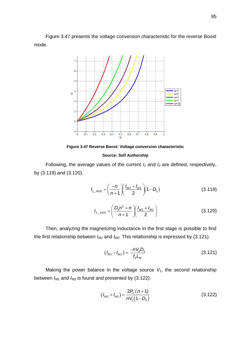
95
Figure 3.47 presents the voltage conversion characteristic for the reverse Boost
mode.
Figure 3.47 Reverse Boost: Voltage conversion characteristic
Source: Self Authorship
Following, the average values of the current I1 and I2 are defined, respectively,
by (3.119) and (3.120).
2 11_ 31
1 2M M
AVG
I InI D
n (3.119)
2
3 2 12 _
1 2M M
AVG
D n n I II
n (3.120)
Then, analyzing the magnetizing inductance in the first stage is possible to find
the first relationship between IM1 and IM2. This relationship is expressed by (3.121).
2 31 2M M
S M
nV DI I
f L (3.121)
Making the power balance in the voltage source V1, the second relationship
between IM1 and IM2 is found and presented by (3.122).
2 1
1 3
2 1
1
C
M M
P nI I
nV D (3.122)
96
Summing (3.121) and (3.122), the instantaneous value of the magnetizing
current IM1 is found and expressed by (3.123).
2
1 2 3 3
1
1 3
2 1 1
2 1
C S M
M
S M
P n f L n VV D DI
V f L D n (3.123)
Then, replacing (3.123) in (3.122), the instantaneous value of the magnetizing
current IM2 is determined by(3.107)
2
1 2 3 3
2
1 3
2 1 1
2 1
C S M
M
S M
P n f L n VV D DI
V f L D n (3.124)
Defined the values of IM1 and IM2, the RMS current in the semiconductors can be
calculated.
Considering the function of IS1(t) given by (3.125):
3
1 3 1 22 13
3 3
0, 0
( ),
1 1 1 1
S
S M MM MS S
S
t D T
I t D I II I n nt D T t T
D T n D n
(3.125)
And replacing (3.125) in (3.44), equation (3.44) can be rewritten as (3.126).
3
3
2
2 1
2 3
1_
0 3 1 2
3
1 110
1 1
S S
S
M M
D T TS
S RMS
S D T M M
I I nt
D T nI dt dt
T D I I n
D n
(3.126)
Then, substituting (3.123) and (3.124) into (3.126), and solving the equation,
IS1_RMS is found and expressed by (3.127).
24 2 2 2
3 1 2 3
1_ 22 2 21 3
11 3
6 1 1 12 1S RMS
M sM C S
n D V V DI
V L f n D L P f n (3.127)
For the switch S2, function of IS2(t) given by (3.128) must be considered.
97
2 1
1 3
3
2
3 1 22 13
3 3
, 0
( )
,1 1 1 1
M M
M S
S
S
M MM MS S
S
n I It nI t D T
D TI t
D I II I n nt D T t T
D T n D n
(3.128)
Now, replacing (3.128) in (3.48), equation (3.48) can be rewritten as (3.129).
3
3
2
2 1
1
30
2 _ 2
3 1 22 1
3 3
1
1 1 1 1
S
S
S
D T
M M
M
S
S RMST
SM MM M
SD T
n I It nI dt
D TI
TD I II I n n
t dtD T n D n
(3.129)
This way, substituting (3.123) and (3.124) into (3.129), and solving the equation,
IS2_RMS is found and expressed by (3.130).
22 2 2 4 2
3 1 2 3 3 3
22 2 2 3 2
3
2
3
2 _
1
3 1 1 2
36 1 4 5 2
1
6 1
M C S
S RMS
M S
D V V n D D n D n
L P f n D n n n n
DI
V L f n (3.130)
Finally, considering the function of IS3(t) given by (3.131):
2 1
1 3
3 3
3
, 0( )
0,
M M
M S
S S
S S
n I It nI t D T
I t D T
D T t T
(3.131)
And replacing (3.131) in (3.52), equation (3.52) can be rewritten as (3.132).
3
3
2
22 1
3 _ 1
30
10
S S
S
D T T
M M
S RMS M
S S D T
n I II t nI dt dt
T D T (3.132)
Then, replacing (3.123) and (3.124) in (3.132), and solving the equation, IS3_RMS
is found and expressed by (3.133).
98
24 2 2 2
3 1 2 33
3 _ 2 22 2 21 3
131
6 1 12 1S RMS
M sM C S
n D V V DD
IV L f D L P f n
(3.133)
3.2.6 Reverse Buck-Boost
In this operating mode, the switch S2 is controlled whereas the switch S3 is
always turned-on. The energy flows from V2 to V1 and this mode presents two
operating stages.
Figure 3.48 presents the gate signal for the Reverse Buck-Boost mode.
TSTS TS
Vg
VgS2
t0 t1 t2
VgS1
t0 t1 t2
VgS3
t0 t1 t2
Vg
Figure 3.48 Reverse Buck-Boost: Gate signals
Source: Self Authorship
Stage 1 [t0, t1]: At t0, S3 is already on and S2 is turned-on. In this moment this
stage begins. In this stage, the current flows through the switch S2 and the switch S3
and the magnetizing current IM decreases linearly from –IM1 to –IM2. Figure 3.49
shows this stage.
V1 V2
+ +
S3
S1 S2
D3
D2
+
+
+ + -
+
- -
-
-
- +
LM
VLT1 VLT2
- -
IM
I1 I2D1
: 1nILT1 ILT2
Figure 3.49 Reverse Buck-Boost: First operating stage
Source: Self Authorship
99
The equivalent circuit of the first stage in the Reverse Buck-Boost mode is the
same that in the second stage of the Forward Buck mode. Then, the mathematical
analyses will not be presented again.
Stage 2 [t1, t2]: At t1, S3 remains on and S2 is turned-off. At this moment, this
stage begins. The current continues to flow through the switch S3 and finds a path
through the diode D1. The magnetizing current increases linearly from –IM2 to –IM1.
Figure 3.50 shows this stage.
V1 V2
+ +
S3
S1 S2
D3
D2
+
+
+ + -
+
- -
-
-
- +
LM
VLT1 VLT2
- -
IM
I1 I2D1
: 1nILT1 ILT2
Figure 3.50 Reverse Buck-Boost: Second operating stage
Source: Self Authorship
The equivalent circuit of the second stage in the Reverse Buck-Boost mode is
the same that in the first stage of the Forward Boost mode. Then, the mathematical
analyses will not be presented again.
Figure 3.51 presents the voltage in the switches and figure 3.52 presents the
voltage in the primary and secondary of the tapped inductor for the Reverse Buck-
Boost mode.
VS2
t0 t1 t2
V1+nV2
n
VS1
t0 t1 t2
V1+nV2
TSTS
Figure 3.51 Reverse Buck-Boost: Theoretical voltage waveforms in the switches S1 and S2
Source: Self Authorship

100
VLT2VLT1
t0 t1 t2t0 t1 t2
V1 nV1
TSTS
-nV2 V2
Figure 3.52 Reverse Buck-Boost: Theoretical voltage waveforms in the tapped inductor
Source: Self Authorship
Figure 3.53 shows the theoretical waveforms of the voltage VLM in the
magnetizing inductance LM and the magnetizing current IM for the Reverse Buck-
Boost mode.
VLM
t0 t1 t2
TS
IM
t0 t1 t2
-IM2
-IM1
TS
-nV2
V1
Figure 3.53 Reverse Buck-Boost: Theoretical waveforms in the magnetizing inductance
Source: Self Authorship
In Figure 3.54 are represented the waveforms of the current I1 and the current I2
for the Reverse Buck-Boost mode.
I1
t0 t1 t2
TS
-IM2
-IM1
I2
t0 t1 t2
TS
nIM1
nIM2
Figure 3.54 Reverse Buck-Boost: Theoretical waveforms of the current I1 and I2
Source: Self Authorship
101
Finally, the currents in the switches for the Reverse Buck-Boost mode are
determined by the figure 3.55.
IS3
t0 t1 t2
TS
IS1
t0 t1 t2
TS
-IM2
-IM1
IS2
t0 t1 t2
TS
nIM1
nIM2
nIM1
nIM2
-IM2
-IM1
Figure 3.55 Reverse Buck-Boost: Theoretical current waveforms in the switches
Source: Self Authorship
Making the Volt-second balance in the magnetizing inductance LM, it is possible
to find the voltage conversion characteristic in the Reverse Buck-Boost mode.
This way, replacing (3.8), (3.9), (3.24) and (3.56) in (3.30) and considering
<VLM>AVG=0, the voltage conversion characteristic is found and presented by (3.135).
2 2 1 21 0S SnV D T V D T (3.134)
1 2
2 21
V nD
V D (3.135)
Figure 3.56 presents the voltage conversion characteristic for the Reverse
Buck-Boost mode.
Then, the average values of the currents I1 and I2 are defined, respectively, by
(3.136) and (3.137).
2 11_ 21
2M M
AVG
I II D (3.136)
2 12 _ 2
2M M
AVG
I II nD (3.137)
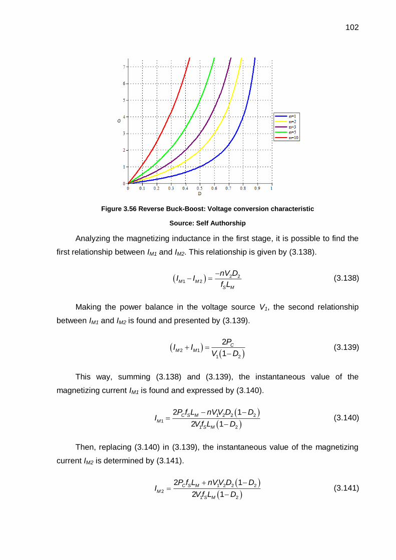
102
Figure 3.56 Reverse Buck-Boost: Voltage conversion characteristic
Source: Self Authorship
Analyzing the magnetizing inductance in the first stage, it is possible to find the
first relationship between IM1 and IM2. This relationship is given by (3.138).
2 21 2M M
S M
nV DI I
f L (3.138)
Making the power balance in the voltage source V1, the second relationship
between IM1 and IM2 is found and presented by (3.139).
2 1
1 2
2
1C
M M
PI I
V D (3.139)
This way, summing (3.138) and (3.139), the instantaneous value of the
magnetizing current IM1 is found and expressed by (3.140).
1 2 2 2
1
1 2
2 1
2 1
C S M
M
S M
P f L nVV D DI
V f L D (3.140)
Then, replacing (3.140) in (3.139), the instantaneous value of the magnetizing
current IM2 is determined by (3.141).
1 2 2 2
2
1 2
2 1
2 1
C S M
M
S M
P f L nVV D DI
V f L D (3.141)

103
Defined the values of IM1 and IM2, the RMS current in the semiconductors can be
calculated.
Considering the function of IS1(t) given by (3.142):
2
1 1 2 22 12
2 2
0, 0
( ),
1 1
S
S M MM MS S
S
t D T
I t I D II It D T t T
D T D
(3.142)
And replacing (3.142) in (3.44), equation (3.44) can be rewritten as (3.143).
2
2
2
2 1 2 22 11_
2 20
10
1 1
S S
S
D T T
M MM MS RMS
S SD T
I D II II dt t dt
T D T D (3.143)
Then, substituting (3.140) and (3.141) into (3.143), and solving the equation,
IS1_RMS is found and given by (3.144).
22 2 2 2
2 1 2 2
1_2 2 2
1 2
11 3
6 1 12S RMS
M s M C S
n D V V DI
V L f D L P f (3.144)
For the switch S2 the function of IS2(t) given by (3.145) must be considered.
2 11 2
2 2
2
, 0( )
0,
M MM S
S S
S S
I In t nI t D T
I t D T
D T t T
(3.145)
Replacing (3.145) in (3.48), equation (3.48) can be rewritten as (3.146).
2
2
2
22 12 _ 1
20
10
S S
S
D T T
M MS RMS M
S S D T
I II n t nI dt dt
T D T (3.146)
Then, substituting (3.140) and (3.141) into (3.146), and solving the equation,
IS2_RMS is found and expressed by (3.147).
2 2 22 2 2 22
2 _ 2 1 2 2
1 2
12
2 3 1
M C SS RMS
M s
L P fDnI n D V V
V L f D (3.147)
104
Finally, considering the function of IS3(t) given by (3.148):
2 11 2
2
3
1 2 22 12
2 2
, 0
( )
,1 1
M MM S
S
S
M MM MS S
S
I In t nI t D T
D TI t
I D II It D T t T
D T D
(3.148)
And replacing (3.148) in (3.52), equation (3.52) can be rewritten as (3.149).
2
2
2
2 2 1
2 12
3 _ 2
0 1 2 21
2
11
1
S S
S
M M
D T TM MS
S RMS S
S D T M MM
I ItI I
D Tn tI dt dtD T
T I D InI
D
(3.149)
Then, replacing (3.140) and (3.141) in (3.149) and solving the equation, IS3_RMS
is found and determined by (3.150).
2 2 2 2 3 2 2 2 3 2 2
2 1 2 2 2 2 2 2 2
2 2 2 2
2 2
2
2
3 _
1
3 2 3 3 1
36 1
1
6
M C S
S RMS
M S
D V V n D n D n D D n D D
L P f D n D
DI
V L f (3.150)
3.3 CHAPTER CONCLUSION
In this chapter, all the theoretical steady state analysis of the bidirectional DC-
DC converter with tapped inductor was presented.
Thinking in an experimental converter implementation, the analysis made in the
present chapter is essential, since with the knowledge provided all the parameters of
the converter become known and, consequently, a design methodology can be
proposed.

105
CHAPTER 4
BIDIRECTIONAL ZVS BUCK-BOOST DC-DC CONVERTER:
STEADY STATE ANALYSIS
4.1 CHAPTER INTRODUCTION
In this chapter, the second topology presented in this thesis is analyzed in
details. As well as the topology presented in chapter 3, this converter is also a
modification of a well-know topology, topology that was presented in Figure 2.10
As mentioned before, the converter presented in Figure 2.10 can just work with
one operation mode for each power flow direction, Buck or Boost, making this
converter unfeasible for applications where one of the voltage sources can present a
wide variation on its value, becoming higher or lower than the other voltage source.
For situations like the one described, in this chapter, a Buck-Boost operation for
both power flow directions is proposed. This operation is allowed just with the
reallocation of the voltage source V2 from the original topology.
Working with the Buck-Boost operation, the converter retains the characteristics
of the original converter. Nevertheless, the proposed converter becomes
conceptually different from the original: in the original converter the voltage sources
are in parallel, whereas in the Buck-Boost operation the voltage sources are in
series.
With this conceptual change, the Buck-Boost converter becomes inappropriate
for applications where the voltage sources are working independent, as, for example,
when they are supplying independent DC buses. However, for applications where the
voltage sources work in conjunction, as a Battery/SC HESS where the SC acts just
like a buffer for the battery, this converter can be used without any restriction.
4.2 BIDIRECTIONAL ZVS BUCK-BOOST DC-DC CONVERTER
Figure 4.1 presents the converter discussed in this chapter.
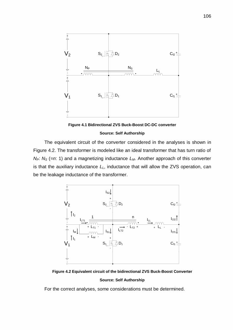
106
S2 D2
S1 D1
V2
-
+
V1
-
+
+
+
Cf2
Cf1
LL
NP NS
Figure 4.1 Bidirectional ZVS Buck-Boost DC-DC converter
Source: Self Authorship
The equivalent circuit of the converter considered in the analyses is shown in
Figure 4.2. The transformer is modeled like an ideal transformer that has turn ratio of
NP: NS (=n: 1) and a magnetizing inductance LM. Another approach of this converter
is that the auxiliary inductance LL, inductance that will allow the ZVS operation, can
be the leakage inductance of the transformer.
V2
V1
S2 D2
S1 D1
-
+
-
+
+
+
Cf2
Cf1
1 n
+ -LM
IM
ILT1
+ -LT1 - +LT2 + -LL
+
-
+
-
ILT2
ILL
IS1
IS2
ICf1
ICf2
I1
I2
Figure 4.2 Equivalent circuit of the bidirectional ZVS Buck-Boost Converter
Source: Self Authorship
For the correct analyses, some considerations must be determined.

107
As the average voltage across an inductor in steady state is equal to zero,
the voltage VCf1 and VCf2 in the capacitors Cf1 and Cf2 will be, respectively,
according to Kirchhoff Voltage Law (KVL), the values of V1 and V2
1 1CfV V (4.1)
2 2CfV V (4.2)
As the average current through a capacitor in steady state is equal to zero
and the inductance LL is connected in a point with two capacitors, the current
ILL is divided equally between Cf1 and Cf2 and has average value equal to
zero.
1 22LL
Cf Cf
II I (4.3)
_ 0LL AVGI (4.4)
The equations of the ideal transformer
1
2
LT P
LT S
V N
V N (4.5)
1 1 2 2LT LT LT LTV I V I (4.6)
Considering NP=1 and NS=n, equations (4.5) and (4.6) can be rewritten,
respectively, as (4.7) and (4.8).
2 1LT LTV nV (4.7)
1 2LT LTI nI (4.8)
As the magnetizing inductance LM is in parallel with the primary of the
transformer, they have the same voltage. Then:
1LT LMV V (4.9)
2LT LMV nV (4.10)

108
4.2.1 Forward Mode
In the forward mode, the energy flows from V1 to V2. The proposed converter
presents 6 stages within one switching period TS for each power flow direction, being
4 operating stages and 2 commutation stages. In the static analysis, as the
commutation stages are very fast they are disregarded for not presenting a
considerable influence in the converter operation. On the other hand, the 4 operating
stages are condensed in just 2 due to the fact that the equivalent circuit when the
current is flowing through the switch or through its antiparallel body diode is the
same, making the mathematical analyses equal for both cases.
Stage 1 [t0, t1]: In this stage, the switch S2 is always turned-off, then, the current
IS2 is equal to zero. The time of this stage is determined by the duty cycle D1 from the
switch S1. The current IS1 flows through the switch S1 or the diode D1. Considering
the direction of the current determined in the equivalent circuit, when the current is
flowing through the diode D1, IS1 is negative. This double direction of the current IS1
will allow the ZVS operation in the converter. Figure 4.3 shows this stage.
V2
V1
S2 D2
S1 D1
-
+
-
+
+
+
Cf2
Cf1
1 n
+ -LM
IM
ILT1
+ -LT1 - +LT2 + -LL
+
-
+
-
ILT2
ILL
IS1
IS2
ICf1
ICf2
I1
I2
Figure 4.3 Forward mode: First stage
Source: Self Authorship
The voltage VLM across the magnetizing inductance LM is determined by
equation (4.11).
1LMV V (4.11)
109
Replacing (4.11) in (4.9) and (4.10), the voltage in each turn of the transformer
is found and determined by (4.12) and (4.13).
1 1LTV V (4.12)
2 1LTV nV (4.13)
The voltage VLL across the auxiliary inductance LL can be determined by (4.14).
1 1 2 1 0LT LT LL CfV V V V V (4.14)
Substituting (4.1), (4.12) and (4.13) into (4.14), VLL is found and given by (4.15).
1 1LLV V n (4.15)
Then, the voltage VS2 in the switch S2 is determined by (4.16).
2 1 2 0S LTV V V (4.16)
Replacing (4.12) in (4.16), VS2 is represented by (4.17).
2 1 2SV V V (4.17)
Analyzing the currents in the equivalent circuit, some relationships can be
found. As the secondary of the transformer LT2 and the inductance LL are in series,
they have the same current, then:
2LT LLI I (4.18)
Replacing (4.18) in (4.8), the current ILT1 in the primary of the transformer is
found and determined by (4.19).
1LT LLI nI (4.19)
The current I2 in the voltage source V2 can be expressed by (4.20).
2 2CfI I (4.20)
Substituting (4.3) into (4.20), I2 can be expressed as function of ILL.
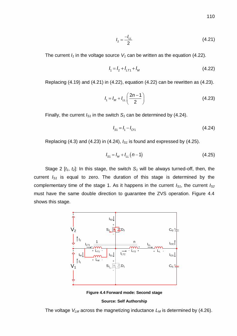
110
22LLI
I (4.21)
The current I1 in the voltage source V1 can be written as the equation (4.22).
1 2 1LT MI I I I (4.22)
Replacing (4.19) and (4.21) in (4.22), equation (4.22) can be rewritten as (4.23).
1
2 1
2M LL
nI I I (4.23)
Finally, the current IS1 in the switch S1 can be determined by (4.24).
1 1 1S CfI I I (4.24)
Replacing (4.3) and (4.23) in (4.24), IS1 is found and expressed by (4.25).
1 1S M LLI I I n (4.25)
Stage 2 [t1, t2]: In this stage, the switch S1 will be always turned-off, then, the
current IS1 is equal to zero. The duration of this stage is determined by the
complementary time of the stage 1. As it happens in the current IS1, the current IS2
must have the same double direction to guarantee the ZVS operation. Figure 4.4
shows this stage.
V2
V1
S2 D2
S1 D1
-
+
-
+
+
+
Cf2
Cf1
1 n
+ -LM
IM
ILT1
+ -LT1 - +LT2 + -LL
+
-
+
-
ILT2
ILL
IS1
IS2
ICf1
ICf2
I1
I2
Figure 4.4 Forward mode: Second stage
Source: Self Authorship
The voltage VLM across the magnetizing inductance LM is determined by (4.26).
111
2LMV V (4.26)
Replacing (4.26) in (4.9) and (4.10), the voltage in each turn of the transformer
is found and determined by equations (4.27) and (4.28).
1 2LTV V (4.27)
2 2LTV nV (4.28)
The voltage VLL across the auxiliary inductance LL can be determined by (4.29).
2 2 0LT LL CfV V V (4.29)
Substituting (4.2) and (4.28) into (4.29), VLL is found and given by (4.30).
2 1LLV V n (4.30)
The voltage VS1 in the switch S1 is determined by equation (4.31).
1 1 1 0LT SV V V (4.31)
Replacing (4.27) in (4.31), VS1 is represented by (4.32).
1 1 2SV V V (4.32)
The current I1 in the voltage source V1 can be expressed by (4.33).
1 1CfI I (4.33)
Substituting (4.3) into (4.33), I1 can be rewritten as (4.34).
12LLI
I (4.34)
The current I2 in the voltage source V2 can be determined by equation (4.35).
2 1 1M LTI I I I (4.35)
Replacing (4.19) and (4.34) in (4.35), I2 is found and presented by (4.36).
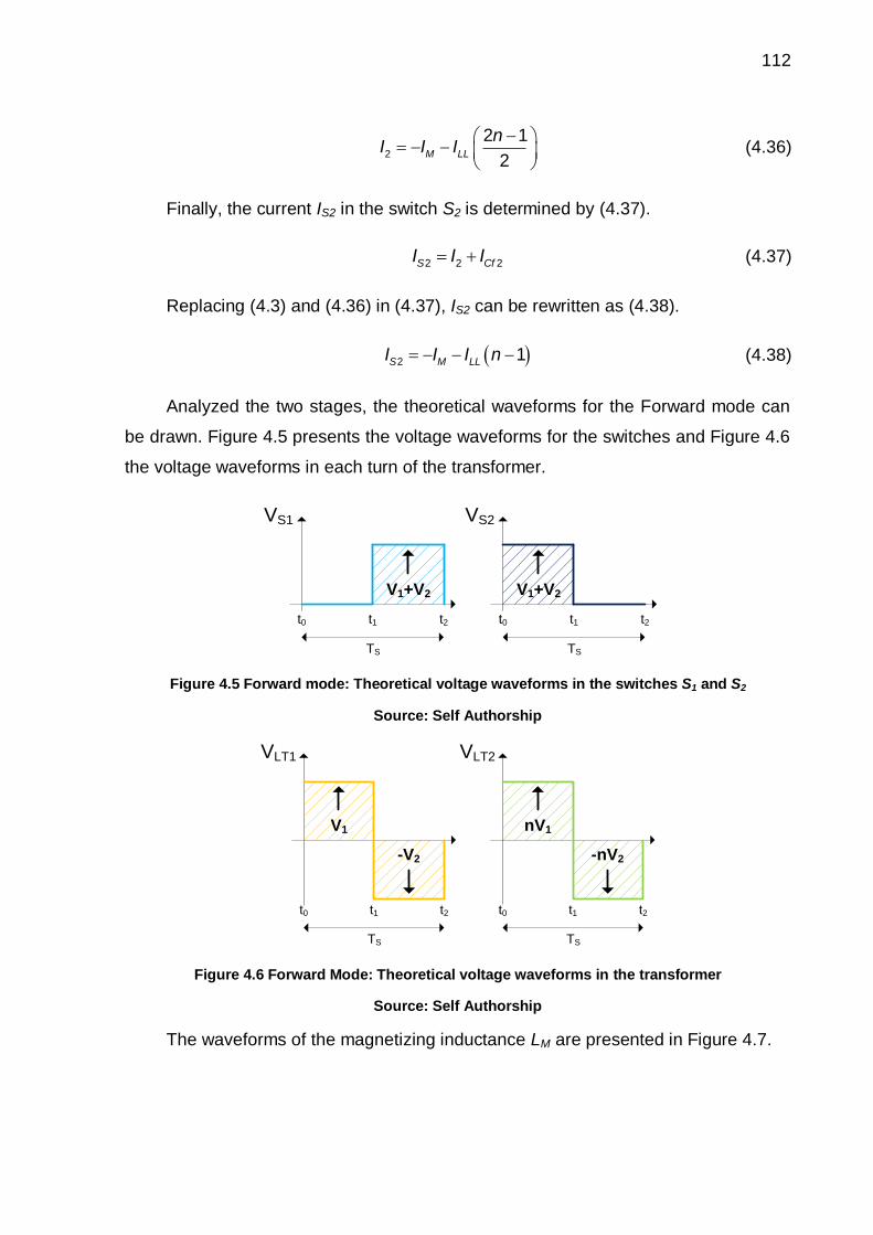
112
2
2 1
2M LL
nI I I (4.36)
Finally, the current IS2 in the switch S2 is determined by (4.37).
2 2 2S CfI I I (4.37)
Replacing (4.3) and (4.36) in (4.37), IS2 can be rewritten as (4.38).
2 1S M LLI I I n (4.38)
Analyzed the two stages, the theoretical waveforms for the Forward mode can
be drawn. Figure 4.5 presents the voltage waveforms for the switches and Figure 4.6
the voltage waveforms in each turn of the transformer.
VS2
t0 t1 t2
TS
V1+V2
VS1
t0 t1 t2
TS
V1+V2
Figure 4.5 Forward mode: Theoretical voltage waveforms in the switches S1 and S2
Source: Self Authorship
VLT2VLT1
t0 t1 t2t0 t1 t2
V1
TSTS
-V2
nV1
-nV2
Figure 4.6 Forward Mode: Theoretical voltage waveforms in the transformer
Source: Self Authorship
The waveforms of the magnetizing inductance LM are presented in Figure 4.7.

113
t0 t1 t2
TS
IM
t0 t1 t2
TS
VLM
IM2
IM1V1
-V2
Figure 4.7 Forward mode: Theoretical waveforms in the magnetizing inductance
Source: Self Authorship
The expected waveforms of the auxiliary inductance LL are presented in Figure
4.8. It is important to note that the behavior of the waveforms will be directly related
with the value of n. When n is bigger than 1, in the first stage the voltage across this
inductance will be positive, consequently, the current ILL will increase linearly in this
stage, and decrease in the second stage.
The opposite happens when n is smaller than 1. In this case, the voltage across
this inductance will be negative in the first stage, consequently the current will
decrease linearly, and increase in the second stage.
t0 t1 t2
TS
ILL
t0 t1 t2
TS
VLL
ILL
-ILL
(n-1)V1
(1-n)V2
(a)
t0 t1 t2
TS
ILL
t0 t1 t2
TS
VLL
ILL
-ILL
(n-1)V1
(1-n)V2
(b)
Figure 4.8 Forward Mode: Theoretical waveforms in the auxiliary inductance (a) n>1 (b) n<1
Source: Self Authorship
Determined the currents IM and ILL, the currents in the voltage sources and in
the switches can be drawn. Figure 4.9 and 4.10 present, respectively, the currents I1
and I2 in the voltage sources V1 and V2 for different values of n.
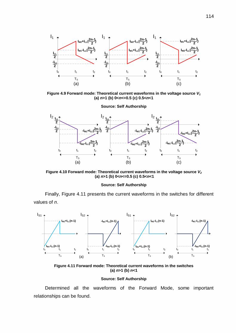
114
I1
t0 t1 t2
TS
(a)
ILL
2
-ILL
2
IM1-ILL( )2n-1
2
IM2+ILL( )2n-1
2
I1
t0 t1 t2
TS
(b)
ILL
2
-ILL
2
IM1+ILL( )2n-1
2
IM2-ILL( )2n-1
2
I1
t0 t1 t2
TS
(c)
ILL
2
-ILL
2
IM2-ILL( )2n-1
2
IM1+ILL( )2n-1
2
Figure 4.9 Forward mode: Theoretical current waveforms in the voltage source V1
(a) n>1 (b) 0<n<=0.5 (c) 0.5<n<1
Source: Self Authorship
I2
t0 t1 t2
TS
(a)
ILL
2
-ILL
2
I2
t0 t1 t2
TS
(b)
ILL
2
-ILL
2
I2
t0 t1 t2
TS
(c)
ILL
2
-ILL
2
-IM2-ILL( )2n-1
2
-IM1+ILL( )2n-1
2-IM1-ILL( )
2n-12
-IM2+ILL( )2n-1
2-IM1-ILL( )
2n-12
-IM2+ILL( )2n-1
2
Figure 4.10 Forward mode: Theoretical current waveforms in the voltage source V2 (a) n>1 (b) 0<n<=0.5 (c) 0.5<n<1
Source: Self Authorship
Finally, Figure 4.11 presents the current waveforms in the switches for different
values of n.
IM2+ILL(n-1)
IS2
t0 t1
TS
IS1
t0 t1 t2
TS (a)
t2
IM1-ILL(n-1)
-IM1+ILL(n-1)
-IM2-ILL(n-1)
IS2
t0 t1
TS
IS1
t0 t1 t2
TS (b)
t2
IM2-ILL(n-1)
IM1+ILL(n-1) -IM2+ILL(n-1)
-IM1-ILL(n-1)
Figure 4.11 Forward mode: Theoretical current waveforms in the switches (a) n>1 (b) n<1
Source: Self Authorship
Determined all the waveforms of the Forward Mode, some important
relationships can be found.
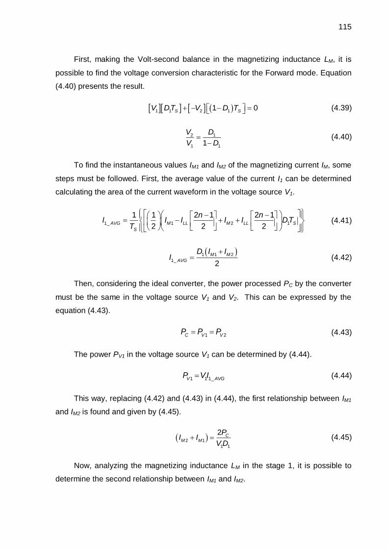
115
First, making the Volt-second balance in the magnetizing inductance LM, it is
possible to find the voltage conversion characteristic for the Forward mode. Equation
(4.40) presents the result.
1 1 2 11 0S SV DT V D T (4.39)
2 1
1 11
V D
V D (4.40)
To find the instantaneous values IM1 and IM2 of the magnetizing current IM, some
steps must be followed. First, the average value of the current I1 can be determined
calculating the area of the current waveform in the voltage source V1.
1_ 1 2 1
1 1 2 1 2 1
2 2 2AVG M LL M LL S
S
n nI I I I I DT
T (4.41)
1 1 2
1_2
M M
AVG
D I II (4.42)
Then, considering the ideal converter, the power processed PC by the converter
must be the same in the voltage source V1 and V2. This can be expressed by the
equation (4.43).
1 2C V VP P P (4.43)
The power PV1 in the voltage source V1 can be determined by (4.44).
1 1 1_V AVGP VI (4.44)
This way, replacing (4.42) and (4.43) in (4.44), the first relationship between IM1
and IM2 is found and given by (4.45).
2 1
1 1
2 CM M
PI I
V D (4.45)
Now, analyzing the magnetizing inductance LM in the stage 1, it is possible to
determine the second relationship between IM1 and IM2.
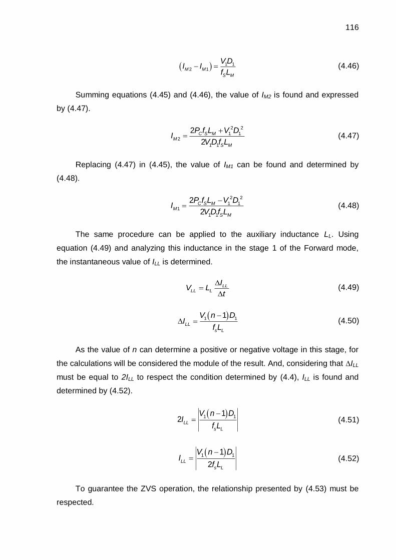
116
1 12 1M M
S M
V DI I
f L (4.46)
Summing equations (4.45) and (4.46), the value of IM2 is found and expressed
by (4.47).
2 2
1 12
1 1
2
2C S M
M
S M
P f L V DI
V D f L (4.47)
Replacing (4.47) in (4.45), the value of IM1 can be found and determined by
(4.48).
2 2
1 11
1 1
2
2C S M
M
S M
P f L V DI
V D f L (4.48)
The same procedure can be applied to the auxiliary inductance LL. Using
equation (4.49) and analyzing this inductance in the stage 1 of the Forward mode,
the instantaneous value of ILL is determined.
LLLL L
IV L
t (4.49)
1 11
LL
s L
V n DI
f L (4.50)
As the value of n can determine a positive or negative voltage in this stage, for
the calculations will be considered the module of the result. And, considering that ∆ILL
must be equal to 2ILL to respect the condition determined by (4.4), ILL is found and
determined by (4.52).
1 11
2 LL
s L
V n DI
f L (4.51)
1 11
2LL
s L
V n DI
f L (4.52)
To guarantee the ZVS operation, the relationship presented by (4.53) must be
respected.

117
1 1 0M LLI I n (4.53)
Replacing (4.48) and (4.52) in (4.53), equation (4.54) is found.
2 21 11 1
1 1
121 0
2 2C S M
S M s L
V n DP f L V Dn
V D f L f L (4.54)
Making the correct mathematical manipulations in (4.54), the value of the
auxiliary inductance that guarantee the ZVS operation is found and determined by
(4.56).
22 2 2 2
1 1 1 12 1 0C S M L L MP f L L V D L V D L n (4.55)
22 2
1 1
2 2
1 1
1
2
M
L
C S M
V D L nL
P f L V D (4.56)
Finally, the RMS value of the currents IS1 and IS2 can be determined.
2
1_ 1
0
1( )
ST
S RMS S
S
I I t dtT
(4.57)
2
2 _ 2
0
1( )
ST
S RMS S
S
I I t dtT
(4.58)
Where the values of IS1 and IS2 can be determined, respectively, by (4.59) and
(4.60).
2 1
1 1
1 1
1
2 11 , 0
( )
0,
M M LL
M LL S
S S
S S
I I I nt I I n t DT
I t DT
DT t T
(4.59)
1
2 1
2
1
2 1
1 1
1
0, 0
2 1( )
1
2 11 ,
1
S
M M LL
S
S
M M LL
M LL S S
t DT
I I I nI t t
D T
I I I nI I n DT t T
D
(4.60)

118
Replacing (4.59) in (4.57) and (4.60) in (4.58), equations (4.57) and (4.58) can
be rewritten, respectively, as (4.61) and (4.62).
1
2
2 1
1_ 1
10
2 111
SD T
M M LL
S RMS M LL
S S
I I I nI t I I n dt
T DT (4.61)
1
2
2 1
1
2 _
2 1
1
1
2 1
11
2 11
1
S
S
M M LL
TS
S RMS
S D T M M LL
M LL
I I I nt
D TI dt
T I I I nI I n
D
(4.62)`
Finally, the RMS values of IS1 and IS2 are determined, respectively, by (4.63)
and (4.64).
4 24 4 2 2
1 1
2 2 2 2
1_
1
1 2 13
1 12
6
M L M L
M L C S
S RMS
S M L
D V L n L L L n
D L L P fI
f L L V (4.63)
4 24 4 2 2
1 1
12 2 2 2
2 _
1 1
1 2 13 1
12
6
M L M L
M L C S
S RMS
S M L
D V L n L L L nD
L L P fI
f L L V D (4.64)
4.2.2 Reverse Mode
In the Reverse mode, the energy flows from V2 to V1 and the controlled switch is
the switch S2. Exactly as the Forward mode, the Reverse mode presents six stages,
being 2 commutation stages and 4 operating stages condensed in just two for the
same reason presented before.
This mode will present inverted stages if compared with the forward mode, that
is, the first stage of the Forward mode will be the second stage in the Reverse mode,
and the second stage of the Forward mode will be the first stage in the Reverse
mode.
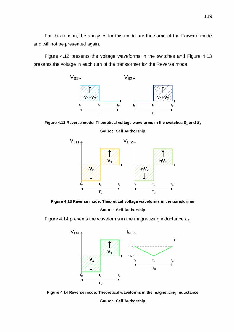
119
For this reason, the analyses for this mode are the same of the Forward mode
and will not be presented again.
Figure 4.12 presents the voltage waveforms in the switches and Figure 4.13
presents the voltage in each turn of the transformer for the Reverse mode.
VS2
t0 t1 t2
VS1
t0 t1 t2
TSTS
V1+V2 V1+V2
Figure 4.12 Reverse mode: Theoretical voltage waveforms in the switches S1 and S2
Source: Self Authorship
VLT2VLT1
t0 t1 t2t0 t1 t2
V1
TSTS
-V2
nV1
-nV2
Figure 4.13 Reverse mode: Theoretical voltage waveforms in the transformer
Source: Self Authorship
Figure 4.14 presents the waveforms in the magnetizing inductance LM.
VLM
t0 t1 t2
TS
IM
t0 t1 t2
-IM2
-IM1
TS
-V2
V1
Figure 4.14 Reverse mode: Theoretical waveforms in the magnetizing inductance
Source: Self Authorship

120
Figure 4.15 presents the waveforms in the auxiliary inductance LL.
t0 t1 t2
TS
ILL
t0 t1 t2
TS
VLL
ILL
-ILL
(1-n)V2
(n-1)V1
(a)
t0 t1 t2
TS
ILL
t0 t1 t2
TS
VLL
ILL
-ILL
(1-n)V2
(n-1)V1
(b)
Figure 4.15 Reverse mode: Theoretical waveforms in the auxiliary inductance (a) n>1 (b) n<1
Source: Self Authorship
Figures 4.16 and 4.17 present, respectively, the waveforms of the current I1 and
I2.
I1
t0 t1 t2
TS
(a)
ILL
2
-ILL
2
I1
t0 t1 t2
TS
(b)
ILL
2
-ILL
2
I1
t0 t1 t2
TS
(c)
ILL
2
-ILL
2
-IM2-ILL( )2n-1
2
-IM1+ILL( )2n-1
2-IM1-ILL( )
2n-12
-IM2+ILL( )2n-1
2-IM1-ILL( )
2n-12
-IM2+ILL( )2n-1
2
Figure 4.16 Reverse mode: Theoretical current waveforms in the voltage source V1 (a) n>1 (b) 0<n<=0.5 (c) 0.5<n<1
Source: Self Authorship
I2
t0 t1 t2
TS
(a)
ILL
2
-ILL
2
I2
t0 t1 t2
TS
(b)
ILL
2
-ILL
2
I2
t0 t1 t2
TS
(c)
ILL
2
-ILL
2
IM2+ILL( )2n-1
2
IM1-ILL( )2n-1
2
IM2-ILL( )2n-1
2IM1+ILL( )
2n-12
IM2-ILL( )2n-1
2IM1+ILL( )
2n-12
Figure 4.17 Reverse mode: Theoretical current waveforms in the voltage source V2 (a) n>1 (b) 0<n<=0.5 (c) 0.5<n<1
Source: Self Authorship
Finally, the current in the switches S1 and S2 are presented by Figure 4.18.
121
IM2+ILL(n-1)
IS1
t0 t1
TS
IS2
t0 t1 t2
TS(a)
t2
IM1-ILL(n-1)
-IM1+ILL(n-1)
-IM2-ILL(n-1)
IS1
t0 t1
TS
IS2
t0 t1 t2
TS(b)
t2
IM2-ILL(n-1)
IM1+ILL(n-1)-IM2+ILL(n-1)
-IM1-ILL(n-1)
Figure 4.18 Reverse mode: Theoretical current waveforms in the switches (a) n>1 (b) n<1
Source: Self Authorship
Making the Volt-second balance in the magnetizing inductance LM, the voltage
conversion characteristic for the Reverse mode is determined by (4.66).
2 2 1 21 0S SV D T V D T (4.65)
1 2
2 21
V D
V D (4.66)
The same procedure used in the Forward mode to find the instantaneous
values of IM1 and IM2 is followed in the reverse mode. First, the average value of the
current I1 is determined by (4.67).
2 1 2
1_
1
2
M M
AVG
D I II (4.67)
To guarantee the correct power balance in the converter, for the Reverse mode
the power PV1 in the voltage source V1 will be considered negative. This can be
expressed by (4.68).
1V CP P (4.68)
Then, making the power balance in the voltage source V1:
1 1 1_V AVGP VI (4.69)
And replacing (4.67) and (4.68) in (4.69), the first relationship between IM1 and
IM2 is found and determined by (4.70).
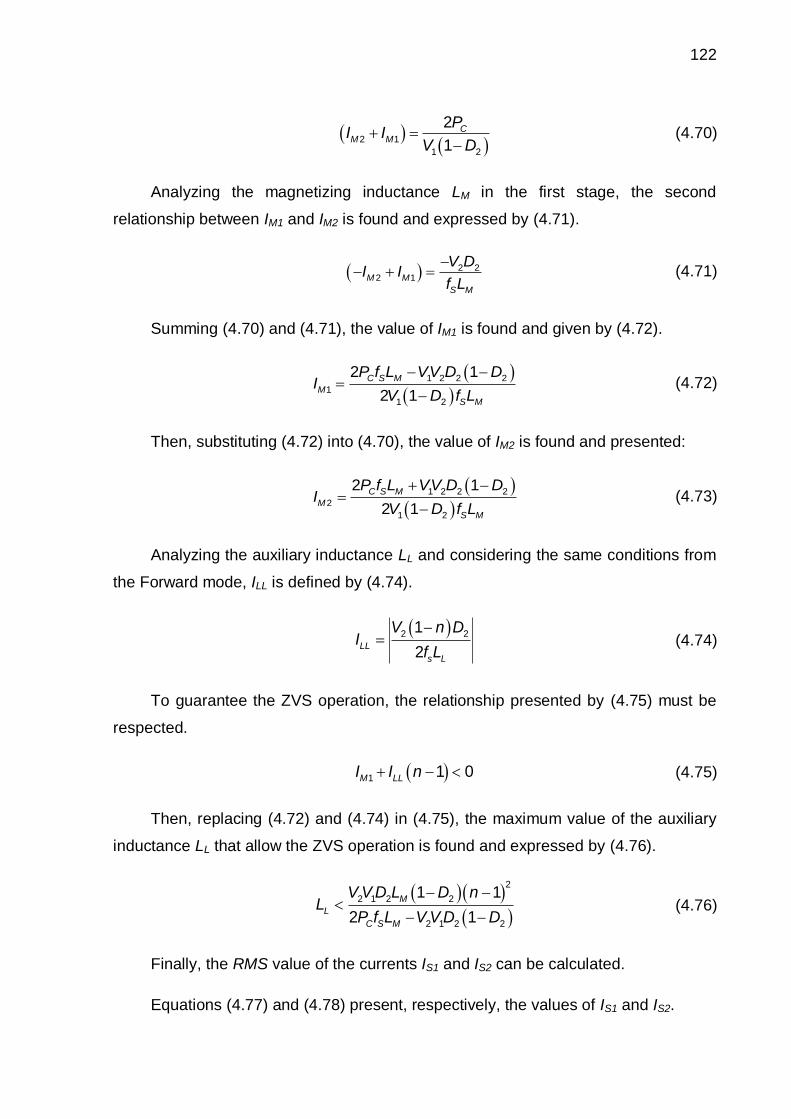
122
2 1
1 2
2
1C
M M
PI I
V D (4.70)
Analyzing the magnetizing inductance LM in the first stage, the second
relationship between IM1 and IM2 is found and expressed by (4.71).
2 22 1M M
S M
V DI I
f L (4.71)
Summing (4.70) and (4.71), the value of IM1 is found and given by (4.72).
1 2 2 2
1
1 2
2 1
2 1
C S M
M
S M
P f L VV D DI
V D f L (4.72)
Then, substituting (4.72) into (4.70), the value of IM2 is found and presented:
1 2 2 2
2
1 2
2 1
2 1
C S M
M
S M
P f L VV D DI
V D f L (4.73)
Analyzing the auxiliary inductance LL and considering the same conditions from
the Forward mode, ILL is defined by (4.74).
2 21
2LL
s L
V n DI
f L (4.74)
To guarantee the ZVS operation, the relationship presented by (4.75) must be
respected.
1 1 0M LLI I n (4.75)
Then, replacing (4.72) and (4.74) in (4.75), the maximum value of the auxiliary
inductance LL that allow the ZVS operation is found and expressed by (4.76).
2
2 1 2 2
2 1 2 2
1 1
2 1
M
L
C S M
V V D L D nL
P f L V V D D (4.76)
Finally, the RMS value of the currents IS1 and IS2 can be calculated.
Equations (4.77) and (4.78) present, respectively, the values of IS1 and IS2.
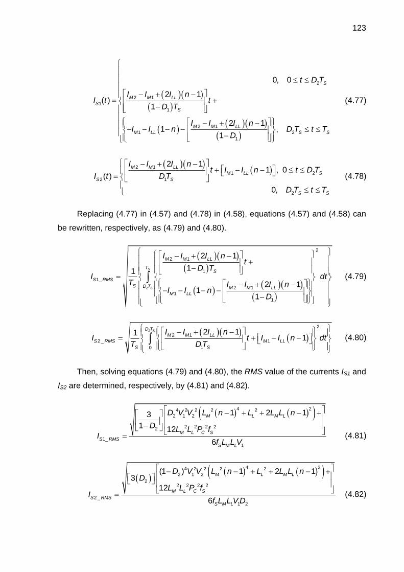
123
2
2 1
1
1
2 1
1 2
1
0, 0
2 1( )
1
2 11 ,
1
S
M M LL
S
S
M M LL
M LL S S
t D T
I I I nI t t
D T
I I I nI I n D T t T
D
(4.77)
2 1
1 2
2 1
2
2 11 , 0
( )
0,
M M LL
M LL S
S S
S S
I I I nt I I n t D T
I t DT
D T t T
(4.78)
Replacing (4.77) in (4.57) and (4.78) in (4.58), equations (4.57) and (4.58) can
be rewritten, respectively, as (4.79) and (4.80).
2
2
2 1
1
1_
2 1
1
1
2 1
11
2 11
1
S
S
M M LL
TS
S RMS
S D T M M LL
M LL
I I I nt
D TI dt
T I I I nI I n
D
(4.79)
2
2
2 1
2 _ 1
10
2 111
SD T
M M LL
S RMS M LL
S S
I I I nI t I I n dt
T DT (4.80)
Then, solving equations (4.79) and (4.80), the RMS value of the currents IS1 and
IS2 are determined, respectively, by (4.81) and (4.82).
4 24 2 2 2 2
2 1 2
2 2 2 22
1_
1
1 2 13
1 12
6
M L M L
M L C S
S RMS
S M L
D V V L n L L L n
D L L P fI
f L L V
(4.81)
4 24 2 2 2 2
2 1 2
22 2 2 2
2 _
1 2
(1 ) 1 2 13
12
6
M L M L
M L C S
S RMS
S M L
D V V L n L L L nD
L L P fI
f L L V D
(4.82)

124
4.3 CHAPTER CONCLUSION
In the present chapter, all the theoretical steady state analysis of the
bidirectional ZVS Buck-Boost DC-DC converter was presented.
As well as in chapter 3, the knowledge provided by this chapter is essential for
an experimental implementation, since all the converter parameters become known
and, consequently, a design methodology can be proposed.
125
CHAPTER 5
BIDIRECTIONAL DC-DC CONVERTER WITH TAPPED INDUCTOR:
DYNAMIC ANALYSIS
5.1 CHAPTER INTRODUCTION
As mentioned earlier in this thesis, in bidirectional DC-DC converters is the
current control that will allow the power flow exchange in the system. However, to
make it possible, a relationship between the current to be controlled and the duty
cycle of the controlled switch must be found.
In order to find this relationship, in this chapter, the dynamic analysis of the
bidirectional DC-DC converter with tapped inductor is presented. Using the instant
average value concept and the small signal approach, the transfer function of each
operation mode of the converter is determined.
5.2 SMALL-SIGNAL ANALYSIS
Considering a Battery/SC HESS in EVs applications, the battery current must
respect some constraints and it is function of the control to guarantee that. Taking
into account the equivalent circuit of the bidirectional DC-DC converter with tapped
inductor presented by Figure 3.2 and imagining a battery as the voltage source 1(V1),
a relationship between the current I1 and the controlled switch for each operation
mode must be found. Nevertheless, before starting the equation method for the
converter, the instant average value concept must be introduced.
According Erickson and Maksimovic (2001), the instant average value concept
can be understood as the average value of a magnitude in a switching period TS.
In this concept, the starting hypothesis is that the time constants of a converter
are much higher than the switching period TS. This way, it is possible to realize the
average of the converter waveforms in a short period of time if compared with the
converter time constant, without significant influence in the system response
(ERICKSON, R. and MAKSIMOVIC, D., 2001).
126
In summary, the resulting average model represents the low frequency behavior
of the converter, disregarding the high frequency harmonics produced by
commutations. The equations that represent the average values of the magnetizing
voltage VLM and the current I1 through the voltage source V1 are given, respectively,
by equations (5.1) and (5.2).
_ _SLM T LM ton on Controlled Switch LM toff off Controlled SwitchV V t V t (5.1)
1 1 _ 1 _ST ton on Controlled Switch toff off Controlled SwitchI I t I t (5.2)
Another important factor for the correct dynamic model of the converter is the
small-signal approach.
Many systems are non-linear, making difficult the use of known control
techniques in their control. However, applying the small signal analysis, linear models
are found by the linearization around an operating point. In this technique, a small
perturbation is applied in the input signal and this perturbation will cause a
perturbation in the output signal, which is already considered linearized (ERICKSON,
R. and MAKSIMOVIC, D., 2001).
In the small signal analysis, a signal can be written as its average value plus a
small perturbation, where the average value is so much bigger than the perturbation.
From equation (5.3) to (5.7), the signals involved for the control of the converter are
rewritten in the small signal form. Assuming that in this work the goal of the control is
the current control of the system and as the voltage across the voltage sources will
not present a significant variation and will not be controlled, for the analyses will not
be considered perturbations on the two voltage sources.
( )M M MI t I i t
(5.3)
1 1 1I t I i t
(5.4)
1 1 1( )D t D d t
(5.5)
2 2 2( )D t D d t
(5.6)

127
3 3 3( )D t D d t
(5.7)
Following, the analyses for each operation mode of the converter are
presented.
5.2.1 Forward Buck
Considering the analyses made in chapter 3, the values of the magnetizing
voltage VLM for each operation stage are already known. This way, for the Forward
Buck, equation (5.1) can be rewritten as (5.8).
1 21 2 1
(V V )1
1
M
M
d I t nL D t nV D t
dt n
(5.8)
Replacing equations (5.3) and (5.5) in (5.8), equation (5.9) is found.
1 21 1 2 1 1
( )(V V )
( ) 1 ( )1
M M
M
d I i tn
L D d t nV D d tdt n
(5.9)
Then, separating the first order terms of (5.9) and applying the Laplace
Transform, the transfer function of the magnetizing current by the controlled duty
cycle of the Forward Buck is found and presented by (5.10).
2 1
1
( )
1( )
M
M
n nV Vi s
n L sd s
(5.10)
The same method is used to find the transfer function of the current I1 through
the voltage source V1 by the duty cycle. First, with the analyses made in chapter 3,
equation (5.2) can be rewritten as (5.11) for the Forward Buck.
1 11
MnI tI t D t
n
(5.11)
Replacing equations (5.4) and (5.5) in (5.11), equation (5.12) is found.
1 1 1 1( ) ( )1
M M
nI i t I i t D d t
n
(5.12)

128
Separating the first order terms and applying the Laplace Transform in (5.12),
(5.13) is found.
1 11
( ) ( )( )
1M MnI d s nD i s
i sn
(5.13)
For the Forward Buck, the value of the magnetizing current can be determined
by (5.14).
1 1
1C
M
P nI
nDV
(5.14)
Finally, replacing (5.10) and (5.14) in (5.13), the transfer function of the current
I1 by the duty cycle is found and presented by (5.15).
2 2 2
1 1 2 11
2
1 11
1( )
1( )
C M
M
P n L s n D V nV Vi s
DV n L sd s
(5.15)
5.2.2 Forward Boost
For the Forward Boost, equation (5.1) can be rewritten as (5.16).
1 21 3 3
(V V )1
1
M
M
d I t nL V D t D t
dt n
(5.16)
Replacing equations (5.3) and (5.7) in (5.16), equation (5.17) is found.
1 21 3 3 3 3
( )(V V )
( ) 1 ( )1
M M
M
d I i tn
L V D d t D d tdt n
(5.17)
Then, separating the first order terms of (5.17) and applying the Laplace
Transform, the transfer function of the magnetizing current by the controlled duty
cycle of the Forward Boost is found and presented by (5.18).
2 1
3
( )
1( )
M
M
i s nV V
n L sd s
(5.18)

129
Doing the same for the current I1 through the voltage source V1, equation (5.2)
can be rewritten as (5.19) for the Forward Boost.
1 3 311
M
M
nI tI t I t D t D t
n
(5.19)
Replacing equations (5.4) and (5.7) in (5.19), equation (5.20) is found.
1 1 3 3 3 3( ) ( ) ( ) 1 ( )1
M M M M
nI i t I i t D d t I i t D d t
n
(5.20)
Then, separating the first order terms and applying the Laplace Transform in
(5.20), (5.21) can be determined.
3 3
1
( ) ( )( )
1
M MI d s n D i si s
n
(5.21)
For the Forward Boost, the value of the magnetizing current can be determined
by (5.22).
1 3
1C
M
P nI
V n D
(5.22)
Finally, replacing (5.18) and (5.22) in (5.21), the transfer function of the current
I1 by the controlled duty cycle for the Forward Boost is given and presented by (5.23).
2 2
1 3 2 11
2
1 33
1( )
1( )
C M
M
P n L s V n D nV Vi s
V n D n L sd s
(5.23)
5.2.3 Forward Buck-Boost
For the Forward Buck-Boost, equation (5.1) can be rewritten as (5.24).
1 1 2 11M
M
d I tL V D t nV D t
dt (5.24)
Then, replacing equations (5.3) and (5.5) in (5.24), equation (5.25) is found.
130
1 1 1 2 1 1
( )
( ) 1 ( )M M
M
d I i t
L V D d t nV D d tdt
(5.25)
Separating the first order terms of (5.25) and applying the Laplace Transform,
the transfer function of the magnetizing current by the duty cycle of the Forward
Buck-Boost is found and presented by (5.26).
2 1
1
( )
( )
M
M
i s nV V
L sd s
(5.26)
Doing the same for the current I1 through the voltage source V1, equation (5.2)
can be rewritten as (5.27) for the Forward Buck-Boost.
1 1MI t I t D t (5.27)
Replacing equations (5.4) and (5.5) in (5.27), equation (5.28) is found.
1 1 1 1( ) ( )M MI i t I i t D d t
(5.28)
Then, separating the first order terms and applying the Laplace Transform in
(5.28), (5.29) can be determined.
1 1 1( ) ( ) ( )M Mi s I d s D i s
(5.29)
For the Forward Buck-Boost, the value of the magnetizing current can be
determined by (5.30).
1 1
CM
PI
V D (5.30)
Finally, replacing (5.26) and (5.30) in (5.29), the transfer function of the current
I1 by the duty cycle for the Forward Buck-Boost is found and presented by (5.31).
2
1 1 2 11
1 11
( )
( )
C M
M
P L s D V nV Vi s
DV L sd s
(5.31)
131
5.2.4 Reverse Buck
For the Reverse Buck, equation (5.1) can be rewritten as (5.32).
1 22 1 2
(V V )1
1
M
M
d I t nL D t V D t
dt n
(5.32)
Replacing equations (5.3) and (5.6) in (5.32), equation (5.33) is found.
1 22 2 1 2 2
( )(V V )
( ) 1 ( )1
M M
M
d I i tn
L D d t V D d tdt n
(5.33)
Separating the first order terms of (5.33) and applying the Laplace Transform,
the transfer function of the magnetizing current by the duty cycle of the Reverse Buck
is found and presented by (5.34).
2 1
2
( )
1( )
M
M
nV Vi s
n L sd s
(5.34)
Doing the same for the current I1 through the voltage source V1, equation (5.2)
can be rewritten as (5.35) for the Reverse Buck.
1 2 211
M
M
nI tI t D t I t D t
n
(5.35)
Then, replacing equations (5.4) and (5.6) in (5.35), equation (5.36) is found.
1 1 2 2 2 2( ) ( ) ( ) 1 ( )1
M M M M
nI i t I i t D d t I i t D d t
n
(5.36)
Separating the first order terms and applying the Laplace Transform in (5.36),
(5.37) can be determined.
2 2
1
( ) 1 ( )( )
1
M MI d s n D i si s
n
(5.37)
For the Reverse Buck, the value of the magnetizing current can be determined
by (5.38).

132
1 2
1
1
C
M
P nI
V n D
(5.38)
This way, replacing (5.34) and (5.38) in (5.37), the transfer function of the
current I1 by the duty cycle for the Reverse Buck is found and presented by (5.39).
2 2
1 2 2 11
2
1 22
1 1( )
1 1( )
C M
M
P n L s V n D nV Vi s
V n D n L sd s
(5.39)
5.2.5 Reverse Boost
For the Reverse Boost, equation (5.1) can be rewritten as (5.40).
1 22 3 3
(V V )1
1
M
M
d I t nL nV D t D t
dt n
(5.40)
Replacing equations (5.3) and (5.7) in (5.40), equation (5.41) is found.
1 22 3 3 3 3
( )(V V )
( ) 1 ( )1
M M
M
d I i tn
L nV D d t D d tdt n
(5.41)
Separating the first order terms of (5.41) and applying the Laplace Transform,
the transfer function of the magnetizing current by the duty cycle of the Reverse
Boost is found and presented by (5.42).
2 1
3
( )
1( )
M
M
n nV Vi s
n L sd s
(5.42)
Doing the same for the current I1 through the voltage source V1, equation (5.2)
can be rewritten as (5.43) for the Reverse Boost.
1 311
MnI tI t D t
n
(5.43)
Replacing equations (5.4) and (5.7) in (5.43), equation (5.44) is found.

133
1 1 3 3( ) 1 ( )1
M M
nI i t I i t D d t
n
(5.44)
Then, separating the first order terms and applying the Laplace Transform in
(5.44), (5.45) can be determined.
3 3
1
( ) 1 ( )( )
1
M MnI d s n D i si s
n
(5.45)
For the Reverse Boost, the value of the magnetizing current can be determined
by (5.46).
1 3
1
1
C
M
P nI
nV D
(5.46)
Then, replacing (5.42) and (5.46) in (5.45), the transfer function of the current I1
by the duty cycle for the Reverse Boost is found and presented by (5.47).
2 22
3 1 2 11
2
3 13
1 1( )
1 1( )
C M
M
P n L s n D V nV Vi s
D V n L sd s
(5.47)
5.2.6 Reverse Buck-Boost
For the Reverse Buck-Boost, equation (5.1) can be rewritten as (5.48).
2 2 1 21M
M
d I tL nV D t V D t
dt (5.48)
Replacing equations (5.3) and (5.6) in (5.48), equation (5.49) is found.
2 2 2 1 2 2
( )
( ) 1 ( )M M
M
d I i t
L nV D d t V D d tdt
(5.49)
Separating the first order terms of (5.49) and applying the Laplace Transform,
the transfer function of the magnetizing current by the duty cycle of the Reverse
Buck-Boost is found and presented by (5.50).
134
2 1
2
( )
( )
M
M
nV Vi s
L sd s
(5.50)
Doing the same for the current I1 through the voltage source V1, equation (5.2)
can be rewritten as (5.51) for the Reverse Buck-Boost.
1 21MI t I t D t (5.51)
Replacing equations (5.4) and (5.6) in (5.51), equation (5.52) is found.
1 1 2 2( ) 1 ( )M MI i t I i t D d t
(5.52)
Then, separating the first order terms and applying the Laplace Transform in
(5.52), (5.53) can be determined.
1 2 2( ) ( ) 1 ( )M Mi s I d s D i s
(5.53)
For the Reverse Buck-Boost, the value of the magnetizing current can be
determined by (5.54).
1 21
CM
PI
V D
(5.54)
Finally, replacing (5.50) and (5.54) in (5.53), the transfer function of the current
I1 by the duty cycle for the Reverse Buck-Boost is found and presented by (5.55).
2
2 1 2 11
2 12
1( )
1( )
C M
M
P L s D V nV Vi s
D V L sd s
(5.55)
5.3 CHAPTER CONCLUSION
As it is well-known in the literature, different kinds of systems are required to
respect certain operating parameters, and it is function of the control to guarantee
that. However, to make it possible, a relationship, in the form of an equation, between
the parameter to be controlled and the controlled device must be found.

135
Then, in this chapter, all the dynamic analysis of the bidirectional DC-DC
converter with tapped inductor was presented. The dynamic analysis of the system is
a key factor in the system implementation, since it is the dynamic model which will
make possible to find the equations for the control design.
With the equations performed in this chapter, it is possible to design the control
of the converter, since the equations performed are a relationship between the
current to be controlled and the duty cycle from the controlled switches.

136
CHAPTER 6
BIDIRECTIONAL DC-DC CONVERTER WITH TAPPED INDUCTOR:
DESIGN METHODOLOGY AND SIMULATION RESULTS
6.1 CHAPTER INTRODUCTION
In order to prove the veracity of the analyses made in chapter 3, in this chapter
a design methodology for the bidirectional DC-DC converter with tapped inductor is
proposed. Then, using the power electronics simulation software PSIM®, the
theoretical results are validated with a digital simulation.
6.2 DESIGN METHODOLOGY
To start a design methodology, the design specifications must be determined.
These specifications are determined to fit the needs of a given application, in the
case of this thesis a Battery/SC HESS for EVs.
As determined in chapter 5 the voltage source V1 corresponds to the battery
bank voltage. In order to determine the value of V1, it is necessary to know the
battery voltage levels in some commercial vehicles, as presented in Table 6.1
Table 6.1 Battery bank in the traction system of commercial EVs and HEVs
Vehicle/Year Battery Type Battery Voltage
HEV Toyota Prius 3rd
generation NiMH 201.6 V
HEV Toyota Camry 2012 NiMH 244.8 V
HEV Ford Fusion 2012 NiMH 275 V
EV Honda Fit 2013 Li-ion 331 V
EV Nissan Leaf 2012 Li-ion 360 V
EV BMW i3 2013 Li-ion 360 V
Source: Self Authorship
Analyzing the values presented in Table 6.1, it was chosen a value of 300 V for
the voltage source V1.

137
As this research is a partnership between UTFPR-PG and Concordia
University, to determine the value of the voltage source V2 (SC side) was considered
the availability of SCs in the P. D. Ziogas Power Electronics Laboratory at Concordia
University. Considering the availability of two 48 V SCs at Concordia University and
thinking in a future implementation using those SCs, it was decided to use the value
of 96 V for the voltage source V2.
The rated power PC of the converter was determined in 1000 W due to some
limitations of implementation, such as availability of components for the experimental
setup in the UTFPR-PG Research Center.
About the switching frequency of the converter, the first idea of this project was
the implementation of the converter using the Real-Time Interface (RTI) DSPACE®
for its control, and then the switching frequency fs was determined in 20 kHz
(maximum switching frequency to a good performance of the DSPACE®). Later, it
was decided to change the DSPACE® for a Digital Signal Processor (DSP), but the
switching frequency was maintained the same.
To determine the value of the turn ratio n of the converter, it was considered the
value of the duty cycle to the maximum efficiency of the converter. As it is well-known
that Buck-Boost converters present the maximum efficiency when operating with a
duty cycle of 0.5, rewriting equation (3.32) and applying this concept, it is possible to
find the turn ratio n for the maximum efficiency of the converter.
1 1 2
2 1
300 0.5 961.125
1 96 1 0.5
V D Vn
V D
(6.1)
However, it was decided to sacrifice a bit the efficiency of the converter and
reduce the turn ratio n to 1, mainly to facilitate the building of the tapped inductor,
since with a turn ratio of 1 the turns of the inductor can be made together.
Finally, due to the availability of cores and wires in the UTFPR Research Center
for the building of the tapped inductor, it was determined a magnetizing current ripple
of 35%.
In Table 6.2 the design specifications determined in this section are
summarized.
138
Table 6.2 Design specifications for the bidirectional DC-DC converter with tapped inductor
Specification Symbol Value
Voltage Source 1 V1 300 V
Voltage Source 2 V2 96 V
Rated Power PC 1000 W
Switching Frequency fs 20 kHz
Turn ratio n 1
Magnetizing Current Ripple
∆IM 35%
Source: Self Authorship
6.2.1 Sizing of Components
Considering the values determined in Table 6.2, the bidirectional DC-DC
converter with tapped inductor can operate with 4 of the 6 operating modes: Buck
and Buck-Boost in the Forward mode; Boost and Buck-Boost in the Reverse mode.
Nevertheless, it would be unfeasible to make a sizing of components for each mode
since it would remove one of the main features of this converter, its versatility.
Taking this into account, to the sizing of components it was decided to use the
Forward Buck mode. In equation (6.2), the duty cycle of switch S1 for this mode that
fits the design specifications is determined.
2
1
1 2
1 96 1 10.4848
300 1 96
V nD
V nV
(6.2)
6.2.1.1 Magnetizing inductance LM
With the design specifications determined in Table 6.1 and the value found by
(6.2), the value of the magnetizing inductance LM for the correct working of the
converter can be determined. For this, the value of the average magnetizing current
must be calculated first, as given by (6.3):
_
1 1
1 1000 1 113.75A
1 300 0.4848
C
M AVG
P nI
nDV
(6.3)
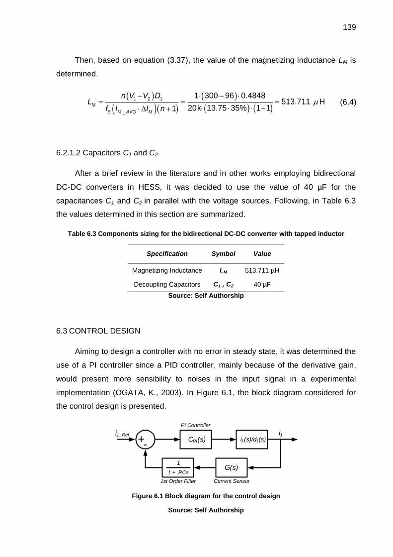
139
Then, based on equation (3.37), the value of the magnetizing inductance LM is
determined.
1 2 1
_
1 300 96 0.4848513.711 H
20k 13.75 35% 1 11M
S M AVG M
n V V DL
f I I n
(6.4)
6.2.1.2 Capacitors C1 and C2
After a brief review in the literature and in other works employing bidirectional
DC-DC converters in HESS, it was decided to use the value of 40 µF for the
capacitances C1 and C2 in parallel with the voltage sources. Following, in Table 6.3
the values determined in this section are summarized.
Table 6.3 Components sizing for the bidirectional DC-DC converter with tapped inductor
Specification Symbol Value
Magnetizing Inductance LM 513.711 µH
Decoupling Capacitors C1 , C2 40 µF
Source: Self Authorship
6.3 CONTROL DESIGN
Aiming to design a controller with no error in steady state, it was determined the
use of a PI controller since a PID controller, mainly because of the derivative gain,
would present more sensibility to noises in the input signal in a experimental
implementation (OGATA, K., 2003). In Figure 6.1, the block diagram considered for
the control design is presented.
Current Sensor
+-CPI(s)
G(s)
i1_Refi1(s)/d1(s)
i1
PI Controller
1st Order Filter
1 + RCs
1
Figure 6.1 Block diagram for the control design
Source: Self Authorship

140
Replacing the values determined by Tables 6.1 and 6.2 in (5.15), the transfer
function of the converter working as the Forward Buck is found and given by (6.5).
41
1
2.055 2.7927 10
0.2989
i s s
d s s
(6.5)
In Figure 6.2, the Bode Diagram of the transfer function presented in (6.5) is
shown.
102
103
104
105
106
-90
-60
-30
0P.M.: inf
Freq: NaN
Frequency (rad/s)
Ph
ase
(d
eg)
15
20
25
30
35
40
45
50
55
G.M.: inf
Freq: NaN
Stable loop
Bode Diagram
Ma
gn
itu
de
(d
B)
Figure 6.2 Bode diagram of the uncompensated system
Source: Self Authorship
Using the SISOTOOL function of the software MatLab®, the controller is
designed. The main goal of the control design is to find a controller with a fast settling
time (less than 5 ms) and little overshoot (around 10%) when applied a step in the
input signal. Besides, for the control design the influence of the current sensor can be
disregarded since it will just represent a gain in the system, and this gain can be
compensated later in the DSP programming. For the 1st Order Filter, a resistor of 10
kΩ and a capacitor of 2.2 nF were considered.
In equation (6.6), the transfer function of the PI controller is presented.
0.05 70
PI
sC s
s
(6.6)
Then, in Figure 6.3, the step response of the compensated system is presented.
Analyzing the Figure 6.3, it was possible to conclude that the controller was designed
in a satisfactory way, where the settling was 2.35 ms and the overshoot 12.1%.

141
Time (ms)
Am
plit
ud
e (
A)
0 0.5 1 1.5 2 2.5 3 3.5
1
1.33
1.67
2
2.33
2.67
3
3.33
3.66
4
Figure 6.3 Step response of the compensated system
Source: Self Authorship
-20
0
20
40
60
80
100
120
Ma
gn
itu
de
(d
B)
101
102
103
104
105
106
-180
-135
-90
-45
0
Ph
ase
(d
eg
)
Bode Diagram
Frequency (rad/s)
Figure 6.4 Bode diagram of the compensated system
Source: Self Authorship
6.4 SIMULATION RESULTS
Before starting the simulation of each mode, it is important first to check if the
control is working, and if the equation (6.5) used for the control design was correctly
developed. First, the circuits implemented in PSIM® for the simulation are presented
in Figures 6.5 and 6.6, where all the elements used are ideal elements.
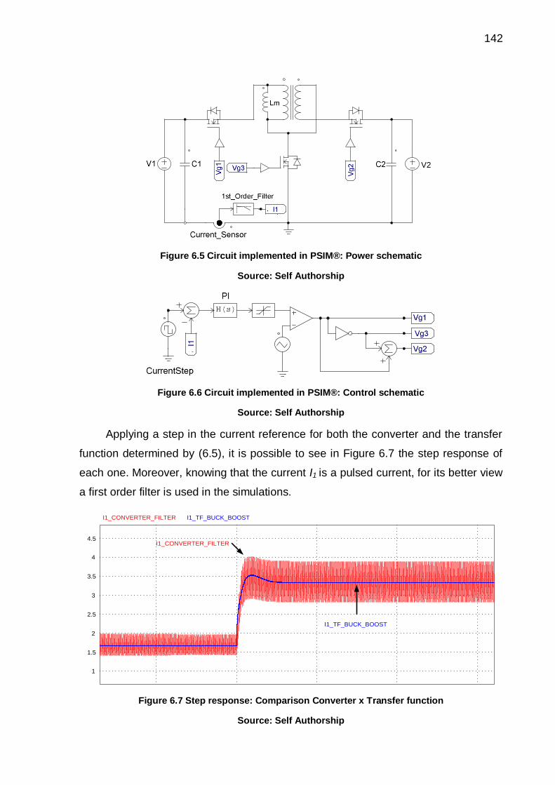
142
V2
Figure 6.5 Circuit implemented in PSIM®: Power schematic
Source: Self Authorship
Figure 6.6 Circuit implemented in PSIM®: Control schematic
Source: Self Authorship
Applying a step in the current reference for both the converter and the transfer
function determined by (6.5), it is possible to see in Figure 6.7 the step response of
each one. Moreover, knowing that the current I1 is a pulsed current, for its better view
a first order filter is used in the simulations.
1
1.5
2
2.5
3
3.5
4
4.5I1_CONVERTER_FILTER
I1_TF_BUCK_BOOST
I1_CONVERTER_FILTER I1_TF_BUCK_BOOST
Figure 6.7 Step response: Comparison Converter x Transfer function
Source: Self Authorship
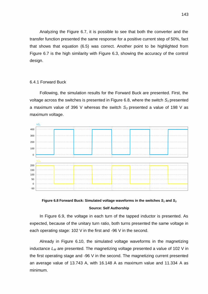
143
Analyzing the Figure 6.7, it is possible to see that both the converter and the
transfer function presented the same response for a positive current step of 50%, fact
that shows that equation (6.5) was correct. Another point to be highlighted from
Figure 6.7 is the high similarity with Figure 6.3, showing the accuracy of the control
design.
6.4.1 Forward Buck
Following, the simulation results for the Forward Buck are presented. First, the
voltage across the switches is presented in Figure 6.8, where the switch S1 presented
a maximum value of 396 V whereas the switch S3 presented a value of 198 V as
maximum voltage.
0
100
200
300
400
VS1
0
-50
50
100
150
200
VS3
Figure 6.8 Forward Buck: Simulated voltage waveforms in the switches S1 and S3
Source: Self Authorship
In Figure 6.9, the voltage in each turn of the tapped inductor is presented. As
expected, because of the unitary turn ratio, both turns presented the same voltage in
each operating stage: 102 V in the first and -96 V in the second.
Already in Figure 6.10, the simulated voltage waveforms in the magnetizing
inductance LM are presented. The magnetizing voltage presented a value of 102 V in
the first operating stage and -96 V in the second. The magnetizing current presented
an average value of 13.743 A, with 16.148 A as maximum value and 11.334 A as
minimum.
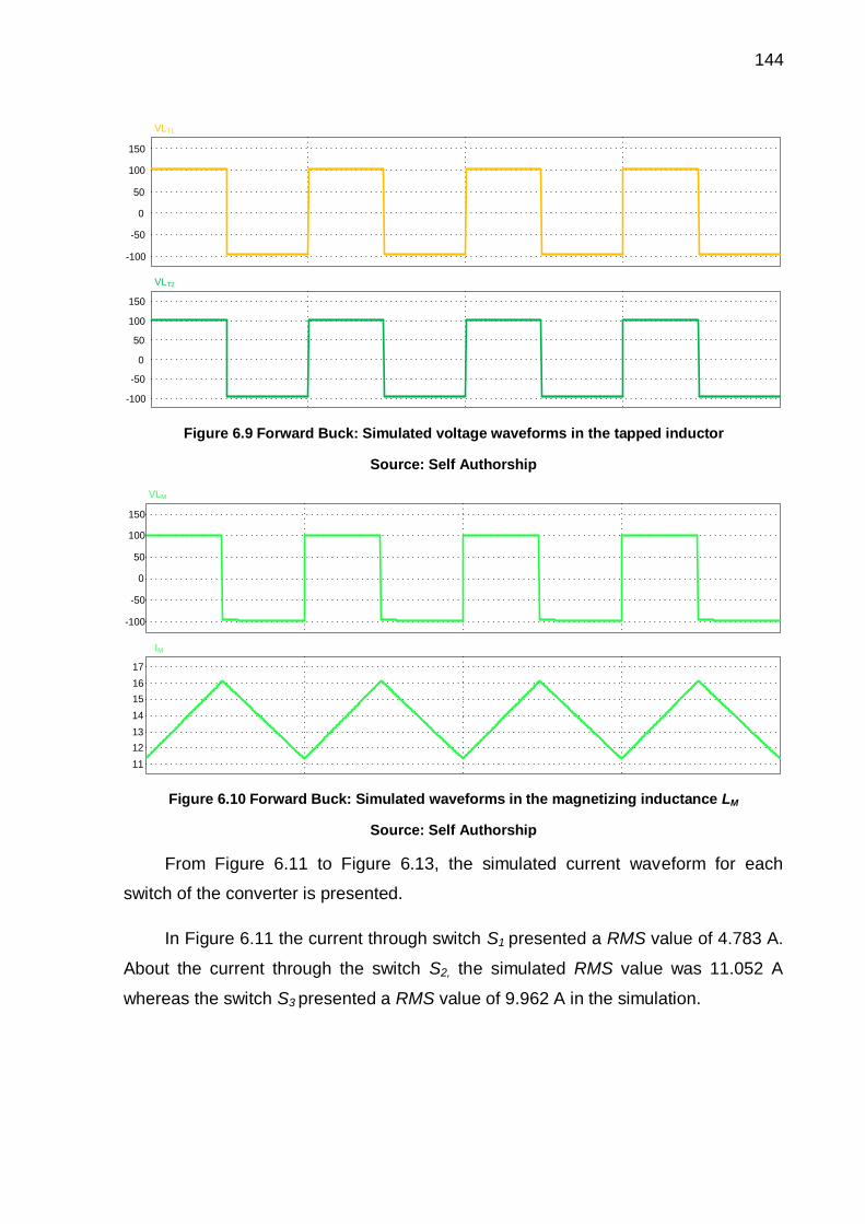
144
0
-50
-100
50
100
150
VLT1
0
-50
-100
50
100
150
VLT2
Figure 6.9 Forward Buck: Simulated voltage waveforms in the tapped inductor
Source: Self Authorship
0
-50
-100
50
100
150
VLM
11
12
13
14
15
16
17
IM
Figure 6.10 Forward Buck: Simulated waveforms in the magnetizing inductance LM
Source: Self Authorship
From Figure 6.11 to Figure 6.13, the simulated current waveform for each
switch of the converter is presented.
In Figure 6.11 the current through switch S1 presented a RMS value of 4.783 A.
About the current through the switch S2, the simulated RMS value was 11.052 A
whereas the switch S3 presented a RMS value of 9.962 A in the simulation.

145
0
2
4
6
8
10
IS1
Figure 6.11 Forward Buck: Simulated current waveform in switch S1
Source: Self Authorship
-18
-16
-14
-12
-10
-8
-6
-4
-2
IS2
Figure 6.12 Forward Buck: Simulated current waveform in switch S2
Source: Self Authorship
0
-5
-10
-15
-20
IS3
Figure 6.13 Forward Buck: Simulated current waveform in switch S3
Source: Self Authorship

146
Next, in Figure 6.14, the current waveforms in the voltage sources are shown.
The current I1 presented a simulated average value of 3.327 A and for the current I2
this value was -10.415 A.
0
2
4
6
8
10
I1
-18
-16
-14
-12
-10
-8
-6
-4
-2
I2
Figure 6.14 Forward Buck: Simulated waveforms of the currents I1 and I2
Source: Self Authorship
To see the current control on the converter, Figure 6.15 is presented. Applying
steps in the current reference from 50% to 100% of the rated power (from 1.665 A to
3.333 A), and vice versa, it is possible to see the action of the control taking the
current from one value to another.
0.1 0.2 0.3 0.4 0.5 0.6 0.7Time (s)
0
1
2
3
4
5I1_CONVERTER_FILTER
I1_CONVERTER_FILTER
I1_REF
I1_REF
Figure 6.15 Forward Buck: Current control
Source: Self Authorship

147
Following, a comparison between the theoretical and the simulated values for
the Forward Buck is presented in Table 6.4. This comparison is important to check if
both theoretical analyses and simulation were performed correctly and, in some
cases, to help to find and solve a possible problem.
Table 6.4 Forward Buck: Comparison Theoretical x Simulated
Symbol Theoretical Simulated Error (%)
VS1_MAX 396 V 396 V -
VS3_MAX 198 V 198 V -
VLT1_1st 102 V 102 V -
VLT1_2nd -96 V -96 V -
VLT2_1st 102 V 102 V -
VLT2_2nd -96 V -96 V -
VLM_1st 102 V 102 V -
VLM_2nd -96 V -96 V -
IM1 11.343 A 11.334 A -0.079
IM2 16.157 A 16.148 A -0.055
IM_AVG 13.75 A 13.743 A -0.050
I1_AVG 3.333 A 3.327 A -0.180
I2_AVG -10.417 A -10.415 A +0.019
IS1_RMS 4.812 A 4.783 A -0.602
IS2_RMS 11.024 A 11.052 A +0.253
IS3_RMS 9.919 A 9.962A +0.443
Source: Self Authorship
6.4.2 Forward Buck-Boost
Just as for the Forward Buck, the simulation results for the Forward Buck-Boost
mode are presented next.
In Figure 6.16, the maximum voltage across the switches is presented, where
both switches presented the maximum value of 396 V.
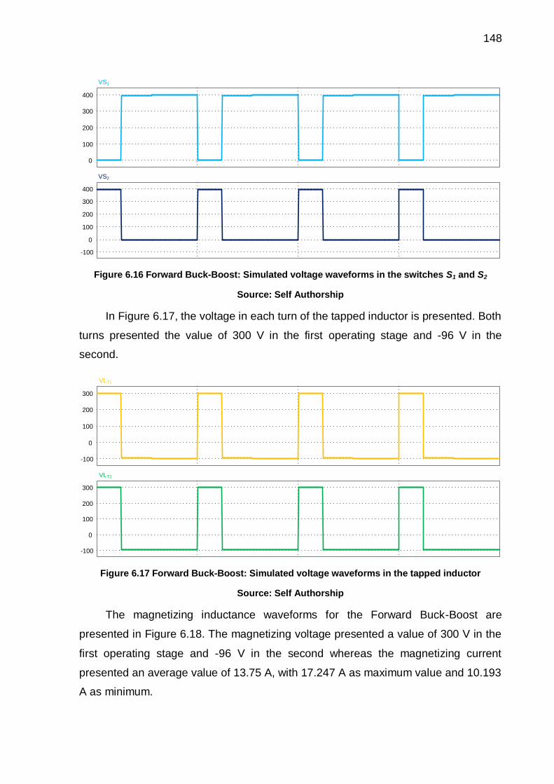
148
0
100
200
300
400
VS1
0
-100
100
200
300
400
VS2
Figure 6.16 Forward Buck-Boost: Simulated voltage waveforms in the switches S1 and S2
Source: Self Authorship
In Figure 6.17, the voltage in each turn of the tapped inductor is presented. Both
turns presented the value of 300 V in the first operating stage and -96 V in the
second.
0
-100
100
200
300
VLT1
0
-100
100
200
300
VLT2
Figure 6.17 Forward Buck-Boost: Simulated voltage waveforms in the tapped inductor
Source: Self Authorship
The magnetizing inductance waveforms for the Forward Buck-Boost are
presented in Figure 6.18. The magnetizing voltage presented a value of 300 V in the
first operating stage and -96 V in the second whereas the magnetizing current
presented an average value of 13.75 A, with 17.247 A as maximum value and 10.193
A as minimum.
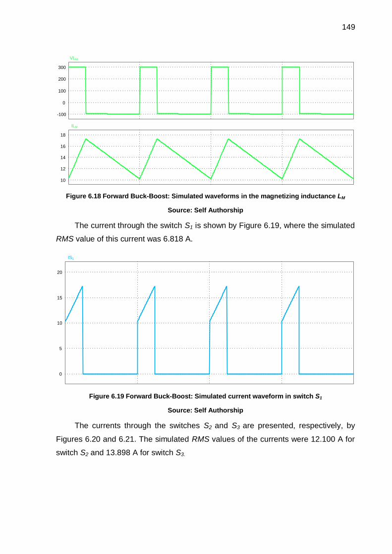
149
0
-100
100
200
300
VLM
10
12
14
16
18
ILM
Figure 6.18 Forward Buck-Boost: Simulated waveforms in the magnetizing inductance LM
Source: Self Authorship
The current through the switch S1 is shown by Figure 6.19, where the simulated
RMS value of this current was 6.818 A.
0
5
10
15
20
IS1
Figure 6.19 Forward Buck-Boost: Simulated current waveform in switch S1
Source: Self Authorship
The currents through the switches S2 and S3 are presented, respectively, by
Figures 6.20 and 6.21. The simulated RMS values of the currents were 12.100 A for
switch S2 and 13.898 A for switch S3.

150
0
-5
-10
-15
-20
IS2
Figure 6.20 Forward Buck-Boost: Simulated current waveform in switch S2
Source: Self Authorship
0
-10
-20
10
20
IS3
Figure 6.21 Forward Buck-Boost: Simulated current waveform in switch S3
Source: Self Authorship
In Figure 6.22, the simulated current waveforms through the voltage sources
are presented.
The current I1 presented an average value of 3.305 A and the current I2 an
average value of -10.432 A.

151
0
5
10
15
20
I1
0
-5
-10
-15
-20
5
I2
Figure 6.22 Forward Buck-Boost: Simulated waveforms of the currents I1 and I2
Source: Self Authorship
Then, in Figure 6.23 it is possible to see the action of the control for the Forward
Buck-Boost mode. As can be seen in Figure 6.23, even the control being designed
for a different operation mode, the control worked well, with no overshoot and
responding fast to a reference change.
0.1 0.2 0.3 0.4 0.5 0.6 0.7Time (s)
0
1
2
3
4
5I1_CONVERTER_FILTER I1_REF
I1_REF
I1_CONVERTER_FILTER
Figure 6.23 Forward Buck-Boost: Current control
Source: Self Authorship
Finally, the comparison between the theoretical values and the simulated values
for the Forward Buck-Boost is presented in Table 6.5.
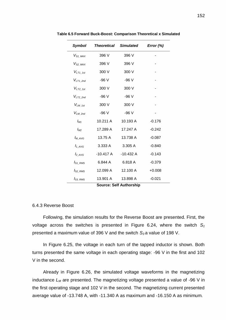
152
Table 6.5 Forward Buck-Boost: Comparison Theoretical x Simulated
Symbol Theoretical Simulated Error (%)
VS1_MAX 396 V 396 V -
VS2_MAX 396 V 396 V -
VLT1_1st 300 V 300 V -
VLT1_2nd -96 V -96 V -
VLT2_1st 300 V 300 V -
VLT2_2nd -96 V -96 V -
VLM_1st 300 V 300 V -
VLM_2nd -96 V -96 V -
IM1 10.211 A 10.193 A -0.176
IM2 17.289 A 17.247 A -0.242
IM_AVG 13.75 A 13.738 A -0.087
I1_AVG 3.333 A 3.305 A -0.840
I2_AVG -10.417 A -10.432 A -0.143
IS1_RMS 6.844 A 6.818 A -0.379
IS2_RMS 12.099 A 12.100 A +0.008
IS3_RMS 13.901 A 13.898 A -0.021
Source: Self Authorship
6.4.3 Reverse Boost
Following, the simulation results for the Reverse Boost are presented. First, the
voltage across the switches is presented in Figure 6.24, where the switch S1
presented a maximum value of 396 V and the switch S3 a value of 198 V.
In Figure 6.25, the voltage in each turn of the tapped inductor is shown. Both
turns presented the same voltage in each operating stage: -96 V in the first and 102
V in the second.
Already in Figure 6.26, the simulated voltage waveforms in the magnetizing
inductance LM are presented. The magnetizing voltage presented a value of -96 V in
the first operating stage and 102 V in the second. The magnetizing current presented
average value of -13.748 A, with -11.340 A as maximum and -16.150 A as minimum.
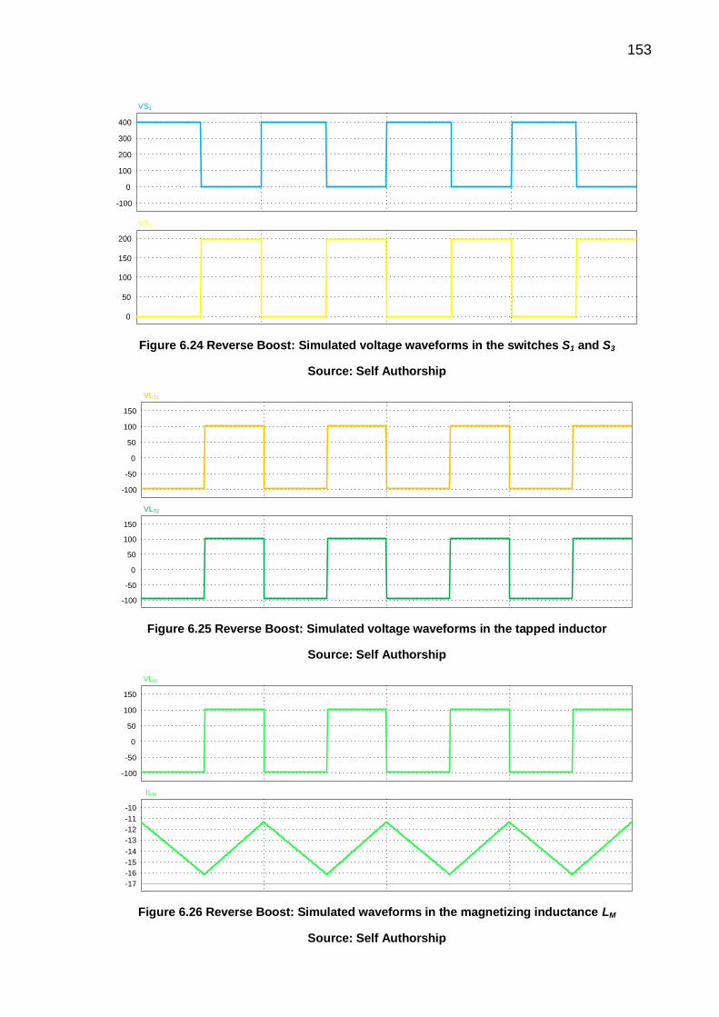
153
0
-100
100
200
300
400
VS1
0
50
100
150
200
VS3
Figure 6.24 Reverse Boost: Simulated voltage waveforms in the switches S1 and S3
Source: Self Authorship
0
-50
-100
50
100
150
VLT1
0
-50
-100
50
100
150
VLT2
Figure 6.25 Reverse Boost: Simulated voltage waveforms in the tapped inductor
Source: Self Authorship
0
-50
-100
50
100
150
VLM
-17
-16
-15
-14
-13
-12
-11
-10
ILM
Figure 6.26 Reverse Boost: Simulated waveforms in the magnetizing inductance LM
Source: Self Authorship

154
The simulated current waveforms for the switches S1 and S2 are presented,
respectively, by Figures 6.27 and 6.28.
0
-2
-4
-6
-8
-10
IS1
Figure 6.27 Reverse Boost: Simulated current waveform in switch S1
Source: Self Authorship
4
6
8
10
12
14
16
18
IS2
Figure 6.28 Reverse Boost: Simulated current waveform in switch S2
Source: Self Authorship
The switch S1 presented a simulated RMS value of 4.803 A whereas in the
switch S2 the RMS current in the simulation was 11.032 A.
In Figure 6.29, the current in switch S3 is shown. This current presented a
simulated RMS value of 9.932 A.

155
0
5
10
15
20
IS3
Figure 6.29 Reverse Boost: Simulated current waveform in switch S3
Source: Self Authorship
Next, in Figure 6.30, the current waveforms in the voltage sources are shown.
The current I1 presented a simulated average value of -3.328 A and for the current I2
this value was 10.420 A.
0
-2
-4
-6
-8
-10
2
I1
4
6
8
10
12
14
16
18
I2
Figure 6.30 Reverse Boost: Simulated waveforms of the currents I1 and I2
Source: Self Authorship
Then, in Figure 6.31 the current control for the Reverse Boost is presented.
Now, as the converter is working in the Reverse mode, negative values are set in the
current reference, but in the same way as the Forward mode, from 50% to 100% of
the rated power (-1.665 A to -3.333A). Again, the control showed a good working,
only presenting an overshoot a way higher than in the Forward mode, but nothing to
concern in the converter operation.

156
0.1 0.2 0.3 0.4 0.5 0.6 0.7Time (s)
0
-1
-2
-3
-4
-5
I1_CONVERTER_FILTER I1_REF
I1_CONVERTER_FILTER
I1_REF
Figure 6.31 Reverse Boost: Current control
Source: Self Authorship
Then, the comparison between the theoretical values and the simulated values
for the Reverse Boost is presented in Table 6.6.
Table 6.6 Reverse Boost: Comparison Theoretical x Simulated
Symbol Theoretical Simulated Error (%)
VS1_MAX 396 V 396 V -
VS3_MAX 198 V 198 V -
VLT1_1st -96 V -96 V -
VLT1_2nd 102 V 102 V -
VLT2_1st -96 V -96 V -
VLT2_2nd 102 V 102 V -
VLM_1st -96 V -96 V -
VLM_2nd 102 V 102 V -
IM1 -11.343 A -11.340 A +0.026
IM2 -16.157 A -16.152 A +0.030
IM_AVG -13.75 A -13.748 A +0.014
I1_AVG -3.333 A -3.328 A +0.150
I2_AVG 10.417 A 10.420 A +0.028
IS1_RMS 4.812 A 4.803 A -0.187
IS2_RMS 11.024 A 11.032 A +0.072
IS3_RMS 9.919 A 9.932 A +0.131
Source: Self Authorship
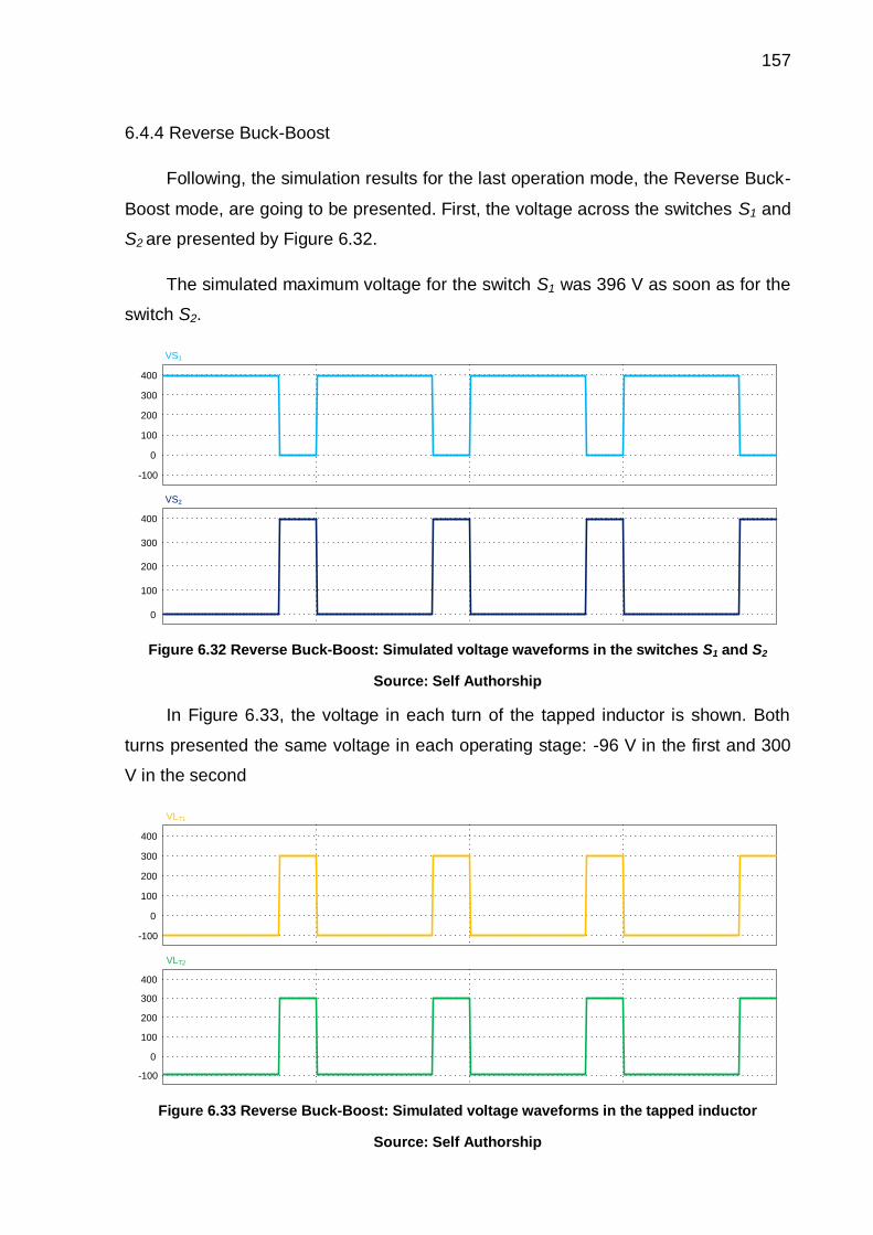
157
6.4.4 Reverse Buck-Boost
Following, the simulation results for the last operation mode, the Reverse Buck-
Boost mode, are going to be presented. First, the voltage across the switches S1 and
S2 are presented by Figure 6.32.
The simulated maximum voltage for the switch S1 was 396 V as soon as for the
switch S2.
0
-100
100
200
300
400
VS1
0
100
200
300
400
VS2
Figure 6.32 Reverse Buck-Boost: Simulated voltage waveforms in the switches S1 and S2
Source: Self Authorship
In Figure 6.33, the voltage in each turn of the tapped inductor is shown. Both
turns presented the same voltage in each operating stage: -96 V in the first and 300
V in the second
0
-100
100
200
300
400
VLT1
0
-100
100
200
300
400
VLT2
Figure 6.33 Reverse Buck-Boost: Simulated voltage waveforms in the tapped inductor
Source: Self Authorship

158
The waveforms of the Reverse Buck-Boost are presented in Figure 6.34. The
magnetizing voltage presented a value of -96 V in the first operating stage and 300 V
in the second. About the magnetizing current, this current presented an average
value of -13.75 A, with -10.207 A as maximum value and -17.261 A as minimum.
0
-100
100
200
300
400
VLM
-18
-16
-14
-12
-10
-8
ILM
Figure 6.34 Reverse Buck-Boost: Simulated waveforms in the magnetizing inductance LM
Source: Self Authorship
The current in switch S1 for the Reverse Buck-Boost mode is shown in Figure
6.35 where the simulated RMS value was 6.864 A.
0
-5
-10
-15
-20
IS1
Figure 6.35 Reverse Buck-Boost: Simulated current waveform in switch S1
Source: Self Authorship
The currents through the switches S2 and S3 are presented, respectively, by
Figures 6.36 and 6.37. The simulated RMS values of the currents were 12.084 A for
switch S2 and 13.897 A for switch S3. In Figure 6.38 the current I1 presented a
simulated average value of -3.353 A and for the current I2 this value was 10.397 A.
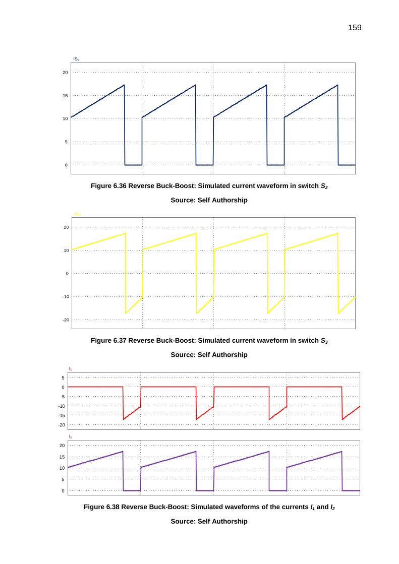
159
0
5
10
15
20
IS2
Figure 6.36 Reverse Buck-Boost: Simulated current waveform in switch S2
Source: Self Authorship
0
-10
-20
10
20
IS3
Figure 6.37 Reverse Buck-Boost: Simulated current waveform in switch S3
Source: Self Authorship
0
-5
-10
-15
-20
5
I1
0
5
10
15
20
I2
Figure 6.38 Reverse Buck-Boost: Simulated waveforms of the currents I1 and I2
Source: Self Authorship
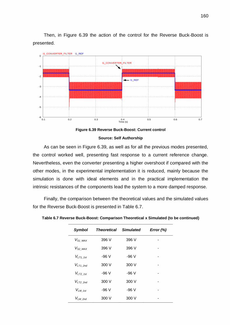
160
Then, in Figure 6.39 the action of the control for the Reverse Buck-Boost is
presented.
0.1 0.2 0.3 0.4 0.5 0.6 0.7Time (s)
0
-1
-2
-3
-4
-5
-6
I1_CONVERTER_FILTER I1_REF
I1_REF
I1_CONVERTER_FILTER
Figure 6.39 Reverse Buck-Boost: Current control
Source: Self Authorship
As can be seen in Figure 6.39, as well as for all the previous modes presented,
the control worked well, presenting fast response to a current reference change.
Nevertheless, even the converter presenting a higher overshoot if compared with the
other modes, in the experimental implementation it is reduced, mainly because the
simulation is done with ideal elements and in the practical implementation the
intrinsic resistances of the components lead the system to a more damped response.
Finally, the comparison between the theoretical values and the simulated values
for the Reverse Buck-Boost is presented in Table 6.7.
Table 6.7 Reverse Buck-Boost: Comparison Theoretical x Simulated (to be continued)
Symbol Theoretical Simulated Error (%)
VS1_MAX 396 V 396 V -
VS2_MAX 396 V 396 V -
VLT1_1st -96 V -96 V -
VLT1_2nd 300 V 300 V -
VLT2_1st -96 V -96 V -
VLT2_2nd 300 V 300 V -
VLM_1st -96 V -96 V -
VLM_2nd 300 V 300 V -
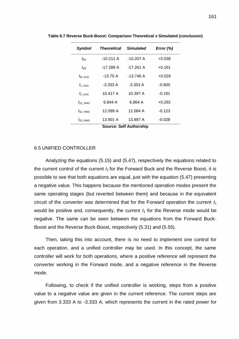
161
Table 6.7 Reverse Buck-Boost: Comparison Theoretical x Simulated (conclusion)
Symbol Theoretical Simulated Error (%)
IM1 -10.211 A -10.207 A +0.039
IM2 -17.289 A -17.261 A +0.161
IM_AVG -13.75 A -13.746 A +0.029
I1_AVG -3.333 A -3.353 A -0.600
I2_AVG 10.417 A 10.397 A -0.191
IS1_RMS 6.844 A 6.864 A +0.292
IS2_RMS 12.099 A 12.084 A -0.123
IS3_RMS 13.901 A 13.897 A -0.028
Source: Self Authorship
6.5 UNIFIED CONTROLLER
Analyzing the equations (5.15) and (5.47), respectively the equations related to
the current control of the current I1 for the Forward Buck and the Reverse Boost, it is
possible to see that both equations are equal, just with the equation (5.47) presenting
a negative value. This happens because the mentioned operation modes present the
same operating stages (but reverted between them) and because in the equivalent
circuit of the converter was determined that for the Forward operation the current I1
would be positive and, consequently, the current I1 for the Reverse mode would be
negative. The same can be seen between the equations from the Forward Buck-
Boost and the Reverse Buck-Boost, respectively (5.31) and (5.55).
Then, taking this into account, there is no need to implement one control for
each operation, and a unified controller may be used. In this concept, the same
controller will work for both operations, where a positive reference will represent the
converter working in the Forward mode, and a negative reference in the Reverse
mode.
Following, to check if the unified controller is working, steps from a positive
value to a negative value are given in the current reference. The current steps are
given from 3.333 A to -3.333 A, which represents the current in the rated power for
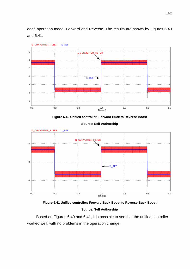
162
each operation mode, Forward and Reverse. The results are shown by Figures 6.40
and 6.41.
0.1 0.2 0.3 0.4 0.5 0.6 0.7Time (s)
0
-2
-4
-6
2
4
6
I1_CONVERTER_FILTER I1_REF
I1_REF
I1_CONVERTER_FILTER
Figure 6.40 Unified controller: Forward Buck to Reverse Boost
Source: Self Authorship
0.1 0.2 0.3 0.4 0.5 0.6 0.7Time (s)
0
-5
5
I1_CONVERTER_FILTER I1_REF
I1_REF
I1_CONVERTER_FILTER
Figure 6.41 Unified controller: Forward Buck-Boost to Reverse Buck-Boost
Source: Self Authorship
Based on Figures 6.40 and 6.41, it is possible to see that the unified controller
worked well, with no problems in the operation change.
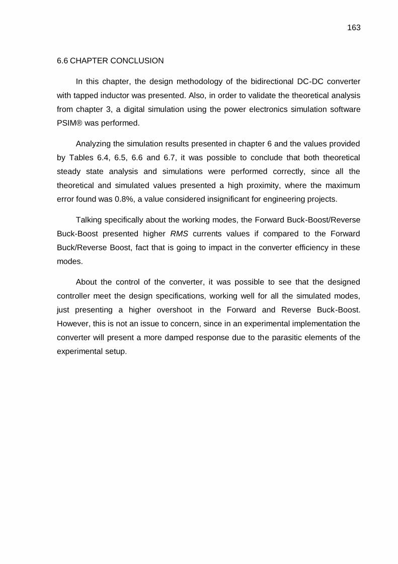
163
6.6 CHAPTER CONCLUSION
In this chapter, the design methodology of the bidirectional DC-DC converter
with tapped inductor was presented. Also, in order to validate the theoretical analysis
from chapter 3, a digital simulation using the power electronics simulation software
PSIM® was performed.
Analyzing the simulation results presented in chapter 6 and the values provided
by Tables 6.4, 6.5, 6.6 and 6.7, it was possible to conclude that both theoretical
steady state analysis and simulations were performed correctly, since all the
theoretical and simulated values presented a high proximity, where the maximum
error found was 0.8%, a value considered insignificant for engineering projects.
Talking specifically about the working modes, the Forward Buck-Boost/Reverse
Buck-Boost presented higher RMS currents values if compared to the Forward
Buck/Reverse Boost, fact that is going to impact in the converter efficiency in these
modes.
About the control of the converter, it was possible to see that the designed
controller meet the design specifications, working well for all the simulated modes,
just presenting a higher overshoot in the Forward and Reverse Buck-Boost.
However, this is not an issue to concern, since in an experimental implementation the
converter will present a more damped response due to the parasitic elements of the
experimental setup.
164
CHAPTER 7
BIDIRECTIONAL ZVS BUCK-BOOST DC-DC CONVERTER:
DESIGN METHODOLOGY AND SIMULATION RESULTS
7.1 CHAPTER INTRODUCTION
In order to prove the veracity of the analyses made in chapter 4, in this chapter
a design methodology for the bidirectional ZVS Buck-Boost DC-DC converter is
proposed. Then, using the power electronics simulation software PSIM®, the
theoretical results are validated with a digital simulation.
7.2 DESIGN METHODOLOGY
In Table 7.1, the specifications for the design of the proposed converter are
presented.
Table 7.1 Design specifications for the bidirectional ZVS Buck-Boost DC-DC converter
Specification Symbol Value
Voltage Source 1 V1 300 V
Voltage Source 2 V2 96 V
Rated Power PC 1000 W
Switching Frequency fs 100 kHz
Magnetizing Current Ripple
∆IM 40%
Source: Self Authorship
Considering that both converters presented in this work are a solution for the
same application, the values of the voltage sources V1 and V2 and the rated power
PC are the same that were used in chapter 6.
Nevertheless, for being a soft-switching converter, the switching frequency fs for
the bidirectional ZVS Buck-Boost DC-DC converter is raised to 100 kHz. Also,
thinking in an experimental implementation and mainly because of the availability of
cores and wires in the UTFPR-PG Research Center, the value of the magnetizing
current ripple is readjusted to 40%.

165
7.2.1 Sizing of Components
With the values determined in Table 7.1, it is possible to calculate the values of
the elements that fit the project needs. However, first the duty cycle values from each
switch must be known.
Based on equation (4.40), the value of the duty cycle D1 is given by (7.1)
21
1 2
960.2424
396
VD
V V
(7.1)
As the switches S1 and S2 work complementarily, the duty cycle D2 can be
determined by (7.2).
2 11 1 0.2424 0.7576D D (7.2)
7.2.1.1 Magnetizing inductance LM
With the design specifications determined in Table 7.1 and the values provided
by (7.1) and (7.2), the value of the magnetizing inductance LM for the correct working
of the converter can be determined. For this, the value of the average magnetizing
current must be calculated first.
_
1 1
100013.75 A
300 0.2424C
M AVG
PI
V D
(7.3)
Then, based on equation (4.46), the value of the magnetizing inductance LM can
be calculated by (7.4).
1 1
_
300 0.2424132.231 H
13.75 40% 100M
M AVG M S
V DL
kI I f
(7.4)
7.2.1.2 Auxiliary inductance LL and number of turns ratio n
As mentioned in chapter 4, the ZVS operation is directly related to the correct
choice of the inductance LL.

166
To determine the value of this inductance, there are two possible approaches:
Setting a randomly value for the turn ratio n and with equation (4.56) find the
maximum value for the inductance LL that allows the ZVS operation;
Setting a randomly value for the inductance LL and with the manipulation of
equation (4.56) find a maximum value for the turn ratio n that allows the ZVS
operation.
In this work, the second one was chosen and a value of 6 µH was determined
for the auxiliary inductance LL.
6LL H (7.5)
Determined the value of the inductance LL, the next step is to determine the
value of the number of turns ratio n. Nevertheless, it is important first to observe the
influence of this parameter on the switches currents.
Figures 7.1 and 7.2 present, respectively, the behavior of the currents IS1_RMS
and IS2_RMS in function of n.
0 0.5 1 1.5 2 2.5 35
9.5
14
18.5
23
27.5
32
36.5
41
45.5
50
IS1RMS n( )
n
Figure 7.1 RMS current in switch S1 for different values of n
Source: Self Authorship
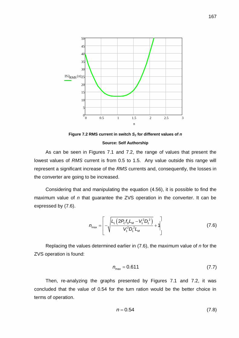
167
0 0.5 1 1.5 2 2.5 30
5
10
15
20
25
30
35
40
45
50
IS2RMS n( )
n
Figure 7.2 RMS current in switch S2 for different values of n
Source: Self Authorship
As can be seen in Figures 7.1 and 7.2, the range of values that present the
lowest values of RMS current is from 0.5 to 1.5. Any value outside this range will
represent a significant increase of the RMS currents and, consequently, the losses in
the converter are going to be increased.
Considering that and manipulating the equation (4.56), it is possible to find the
maximum value of n that guarantee the ZVS operation in the converter. It can be
expressed by (7.6).
2 2
1 1
max 2 2
1 1
21
L C S M
M
L P f L V Dn
V D L
(7.6)
Replacing the values determined earlier in (7.6), the maximum value of n for the
ZVS operation is found:
max 0.611n (7.7)
Then, re-analyzing the graphs presented by Figures 7.1 and 7.2, it was
concluded that the value of 0.54 for the turn ration would be the better choice in
terms of operation.
0.54n (7.8)
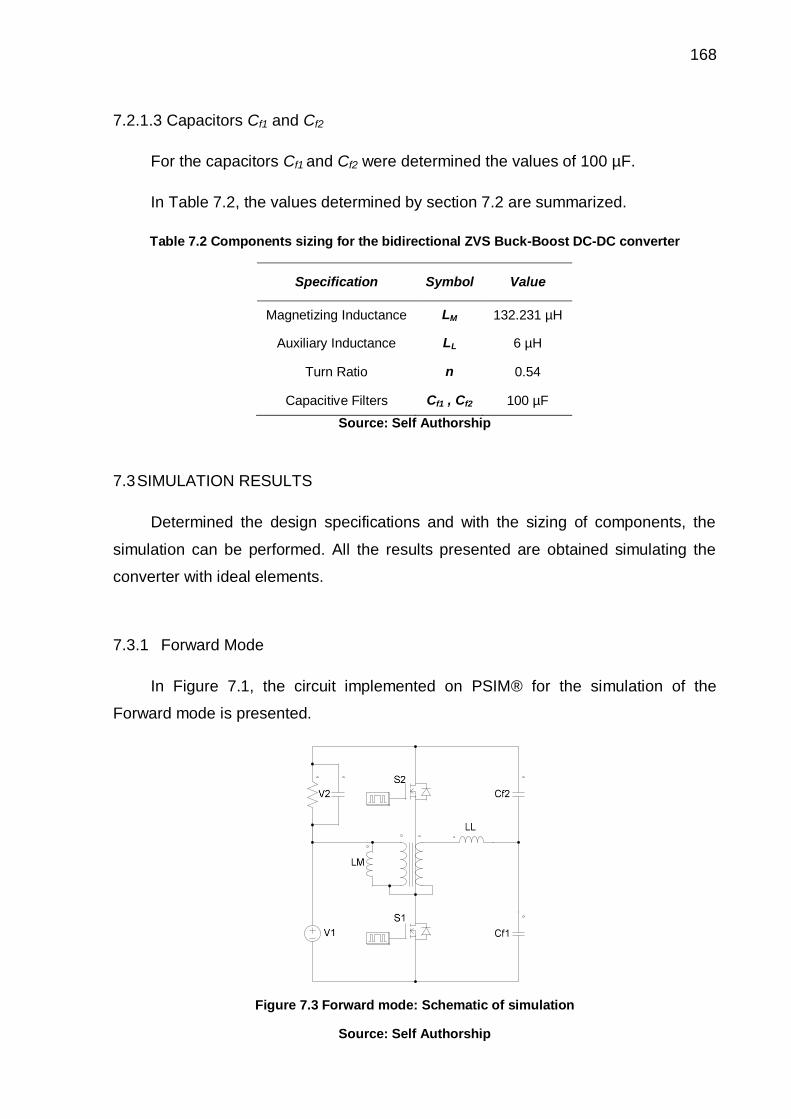
168
7.2.1.3 Capacitors Cf1 and Cf2
For the capacitors Cf1 and Cf2 were determined the values of 100 µF.
In Table 7.2, the values determined by section 7.2 are summarized.
Table 7.2 Components sizing for the bidirectional ZVS Buck-Boost DC-DC converter
Specification Symbol Value
Magnetizing Inductance LM 132.231 µH
Auxiliary Inductance LL 6 µH
Turn Ratio n 0.54
Capacitive Filters Cf1 , Cf2 100 µF
Source: Self Authorship
7.3 SIMULATION RESULTS
Determined the design specifications and with the sizing of components, the
simulation can be performed. All the results presented are obtained simulating the
converter with ideal elements.
7.3.1 Forward Mode
In Figure 7.1, the circuit implemented on PSIM® for the simulation of the
Forward mode is presented.
Figure 7.3 Forward mode: Schematic of simulation
Source: Self Authorship

169
As the simulation is performed in open loop, it is impossible to simulate the
converter with two voltage sources. Taking this into account, for the Forward mode
the voltage source V2 is replaced by a parallel RC load in order to emulate a voltage
source behavior in this side of energy, where the value of the resistance is
determined by equation (7.9) whereas for the capacitance is set a value of 100 µF.
2 2
2 969.216
1000C
VR
P (7.9)
In Figure 7.4, the voltage across the RC load is presented. The voltage
presented the expected value of 96 V, making the simulation possible.
60
80
100
120
V2
Figure 7.4 Forward mode: Voltage across the RC load
Source: Self Authorship
In Figure 7.5, the voltage in each turn of the transformer is presented. The
voltage VLT1 in the primary presented a value of 300 V in the first operating stage and
-96.057 V in the second stage whereas the voltage VLT2 on the secondary presented
the values of 162 V and -51.871 V.
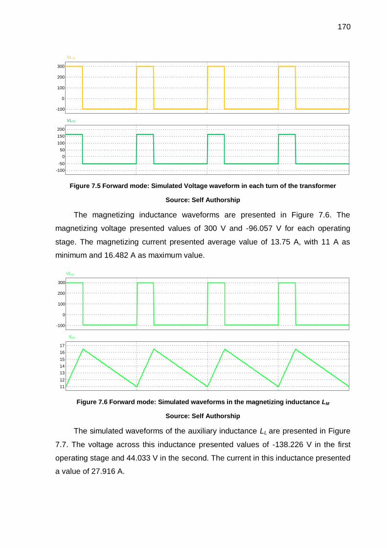
170
0
-100
100
200
300
VLT1
0
-50
-100
50
100
150
200
VLT2
Figure 7.5 Forward mode: Simulated Voltage waveform in each turn of the transformer
Source: Self Authorship
The magnetizing inductance waveforms are presented in Figure 7.6. The
magnetizing voltage presented values of 300 V and -96.057 V for each operating
stage. The magnetizing current presented average value of 13.75 A, with 11 A as
minimum and 16.482 A as maximum value.
0
-100
100
200
300
VLM
11
12
13
14
15
16
17
ILM
Figure 7.6 Forward mode: Simulated waveforms in the magnetizing inductance LM
Source: Self Authorship
The simulated waveforms of the auxiliary inductance LL are presented in Figure
7.7. The voltage across this inductance presented values of -138.226 V in the first
operating stage and 44.033 V in the second. The current in this inductance presented
a value of 27.916 A.
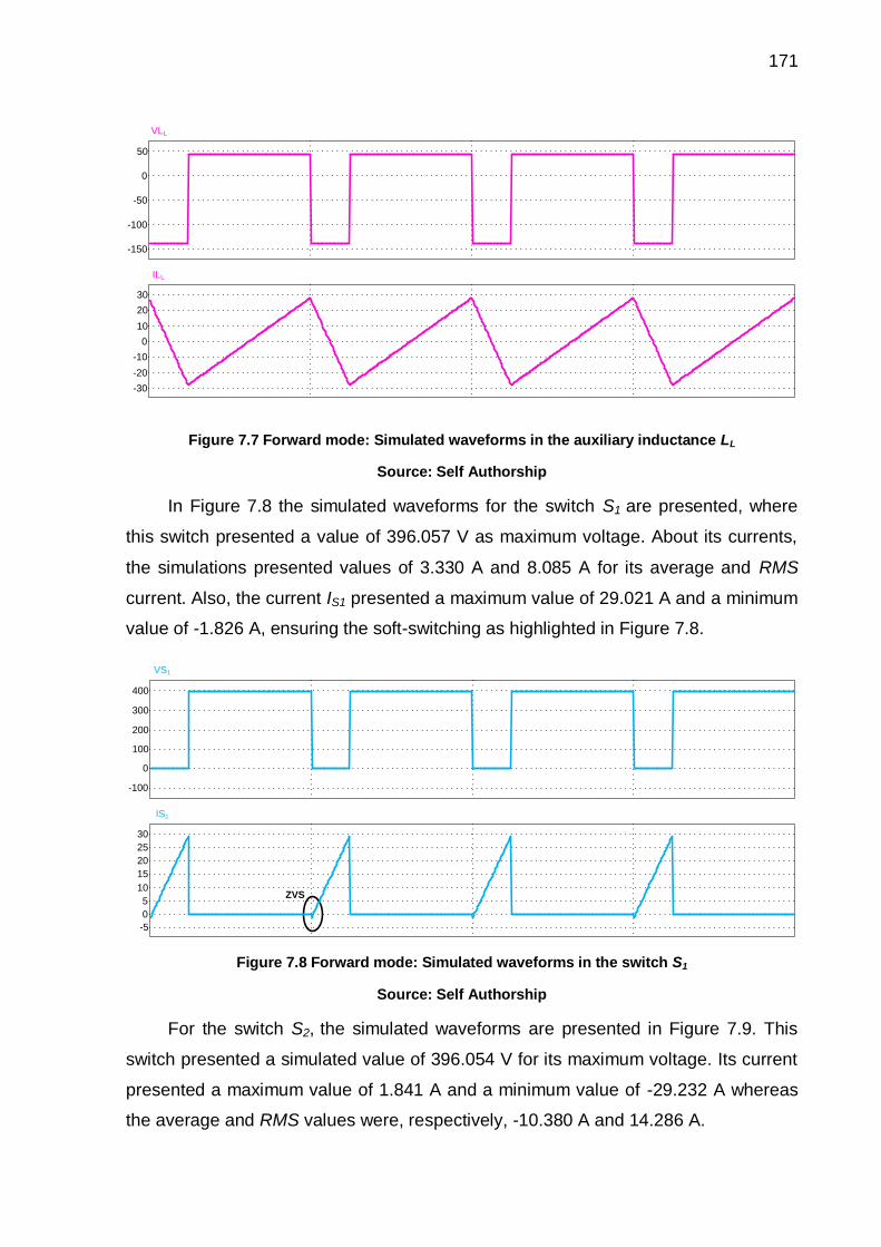
171
0
-50
-100
-150
50
VLL
0
-10
-20
-30
10
20
30
ILL
Figure 7.7 Forward mode: Simulated waveforms in the auxiliary inductance LL
Source: Self Authorship
In Figure 7.8 the simulated waveforms for the switch S1 are presented, where
this switch presented a value of 396.057 V as maximum voltage. About its currents,
the simulations presented values of 3.330 A and 8.085 A for its average and RMS
current. Also, the current IS1 presented a maximum value of 29.021 A and a minimum
value of -1.826 A, ensuring the soft-switching as highlighted in Figure 7.8.
0
-100
100
200
300
400
VS1
0
-5
5
10
15
20
25
30
IS1
ZVS
Figure 7.8 Forward mode: Simulated waveforms in the switch S1
Source: Self Authorship
For the switch S2, the simulated waveforms are presented in Figure 7.9. This
switch presented a simulated value of 396.054 V for its maximum voltage. Its current
presented a maximum value of 1.841 A and a minimum value of -29.232 A whereas
the average and RMS values were, respectively, -10.380 A and 14.286 A.
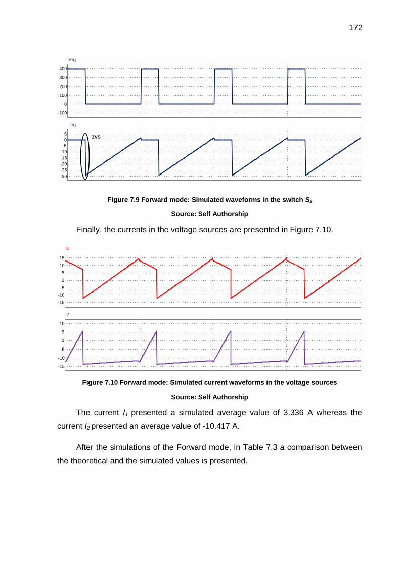
172
ZVS
0
-100
100
200
300
400
VS2
0
-5
-10
-15
-20
-25
-30
5
IS2
Figure 7.9 Forward mode: Simulated waveforms in the switch S2
Source: Self Authorship
Finally, the currents in the voltage sources are presented in Figure 7.10.
0
-5
-10
-15
5
10
15
I1
0
-5
-10
-15
5
10
I2
Figure 7.10 Forward mode: Simulated current waveforms in the voltage sources
Source: Self Authorship
The current I1 presented a simulated average value of 3.336 A whereas the
current I2 presented an average value of -10.417 A.
After the simulations of the Forward mode, in Table 7.3 a comparison between
the theoretical and the simulated values is presented.
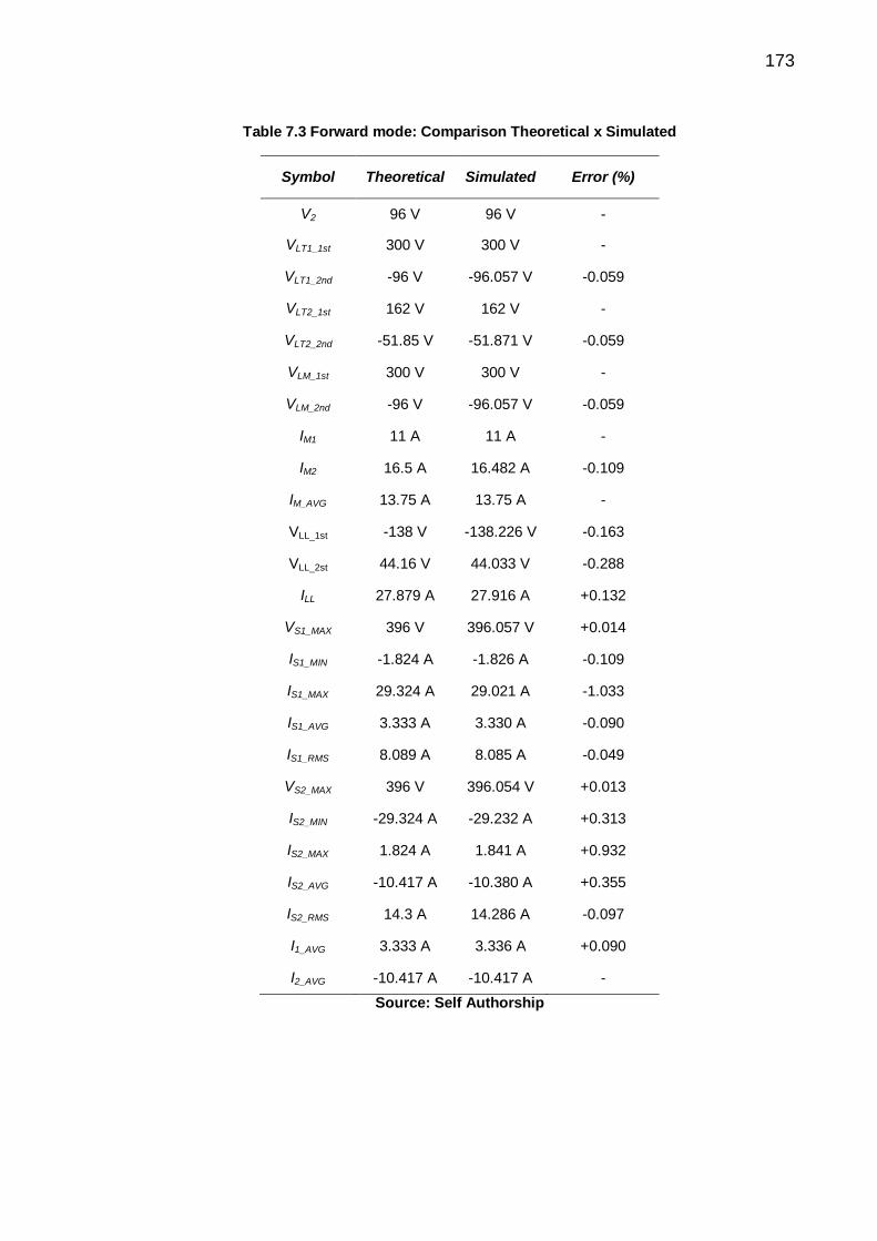
173
Table 7.3 Forward mode: Comparison Theoretical x Simulated
Symbol Theoretical Simulated Error (%)
V2 96 V 96 V -
VLT1_1st 300 V 300 V -
VLT1_2nd -96 V -96.057 V -0.059
VLT2_1st 162 V 162 V -
VLT2_2nd -51.85 V -51.871 V -0.059
VLM_1st 300 V 300 V -
VLM_2nd -96 V -96.057 V -0.059
IM1 11 A 11 A -
IM2 16.5 A 16.482 A -0.109
IM_AVG 13.75 A 13.75 A -
VLL_1st -138 V -138.226 V -0.163
VLL_2st 44.16 V 44.033 V -0.288
ILL 27.879 A 27.916 A +0.132
VS1_MAX 396 V 396.057 V +0.014
IS1_MIN -1.824 A -1.826 A -0.109
IS1_MAX 29.324 A 29.021 A -1.033
IS1_AVG 3.333 A 3.330 A -0.090
IS1_RMS 8.089 A 8.085 A -0.049
VS2_MAX 396 V 396.054 V +0.013
IS2_MIN -29.324 A -29.232 A +0.313
IS2_MAX 1.824 A 1.841 A +0.932
IS2_AVG -10.417 A -10.380 A +0.355
IS2_RMS 14.3 A 14.286 A -0.097
I1_AVG 3.333 A 3.336 A +0.090
I2_AVG -10.417 A -10.417 A -
Source: Self Authorship

174
7.3.2 Reverse Mode
In Figure 7.11, the circuit implemented on PSIM® for the simulation of the
Reverse mode is presented.
Figure 7.11 Reverse mode: Schematic of simulation
Source: Self Authorship
In the same way as the Forward mode, one of the voltage sources must be
replaced by a parallel RC load to make the simulation possible. In the Reverse mode,
the voltage source 1 is replaced by a 90 Ω resistance and the same 100 µF
capacitance.
In Figure 7.12, the voltage across the RC load is presented. The voltage
presented the expected value of 300 V, making the simulation possible.
280
290
300
310
320
V1
Figure 7.12 Reverse mode: Voltage across the RC load
Source: Self Authorship
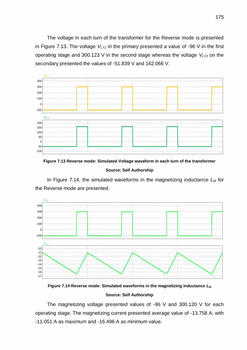
175
The voltage in each turn of the transformer for the Reverse mode is presented
in Figure 7.13. The voltage VLT1 in the primary presented a value of -96 V in the first
operating stage and 300.123 V in the second stage whereas the voltage VLT2 on the
secondary presented the values of -51.839 V and 162.066 V.
0
-100
100
200
300
400
VLT1
0
-50
-100
50
100
150
200
VLT2
Figure 7.13 Reverse mode: Simulated Voltage waveform in each turn of the transformer
Source: Self Authorship
In Figure 7.14, the simulated waveforms in the magnetizing inductance LM for
the Reverse mode are presented.
0
-100
100
200
300
400
VLM
-17
-16
-15
-14
-13
-12
-11
-10
ILM
Figure 7.14 Reverse mode: Simulated waveforms in the magnetizing inductance LM
Source: Self Authorship
The magnetizing voltage presented values of -96 V and 300.120 V for each
operating stage. The magnetizing current presented average value of -13.758 A, with
-11.051 A as maximum and -16.496 A as minimum value.
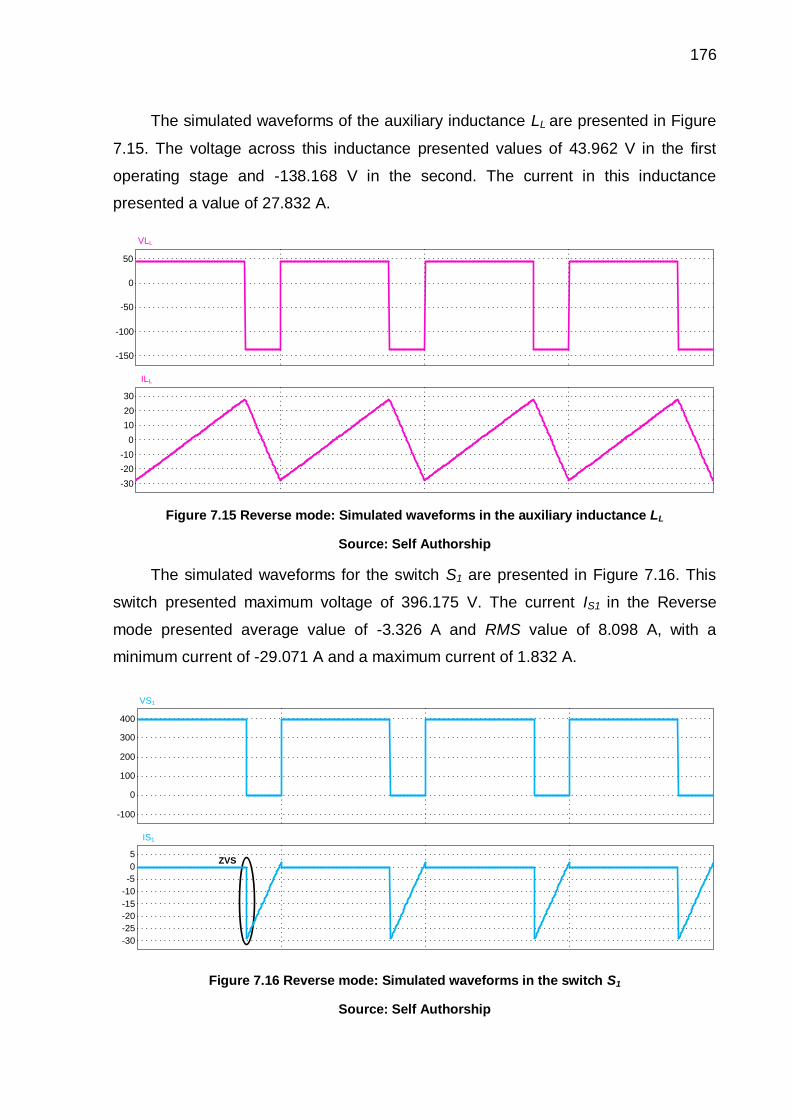
176
The simulated waveforms of the auxiliary inductance LL are presented in Figure
7.15. The voltage across this inductance presented values of 43.962 V in the first
operating stage and -138.168 V in the second. The current in this inductance
presented a value of 27.832 A.
0
-50
-100
-150
50
VLL
0
-10
-20
-30
10
20
30
ILL
Figure 7.15 Reverse mode: Simulated waveforms in the auxiliary inductance LL
Source: Self Authorship
The simulated waveforms for the switch S1 are presented in Figure 7.16. This
switch presented maximum voltage of 396.175 V. The current IS1 in the Reverse
mode presented average value of -3.326 A and RMS value of 8.098 A, with a
minimum current of -29.071 A and a maximum current of 1.832 A.
0
-100
100
200
300
400
VS1
0
-5
-10
-15
-20
-25
-30
5
IS1
ZVS
Figure 7.16 Reverse mode: Simulated waveforms in the switch S1
Source: Self Authorship

177
For the switch S2 the simulated waveforms are presented in Figure 7.17. This
switch presented simulated maximum voltage of 396.123 V. Its current presented a
maximum value of 29.272 A and a minimum value of -1.830 A whereas the average
and RMS values were, respectively, 10.410 A and 14.308 A.
ZVS
0
-100
100
200
300
400
VS2
0
-5
5
10
15
20
25
30
IS2
Figure 7.17 Reverse mode: Simulated waveforms in the switch S2
Source: Self Authorship
Finally, the currents in the voltage sources are presented in Figure 7.18. The
current I1 presented a simulated average value of -3.344 A whereas the current I2
presented an average value of 10.438 A.
0
-5
-10
-15
5
10
I1
0
-5
-10
5
10
15
20
I2
Figure 7.18 Reverse mode: Simulated current waveforms in the voltage sources
Source: Self Authorship
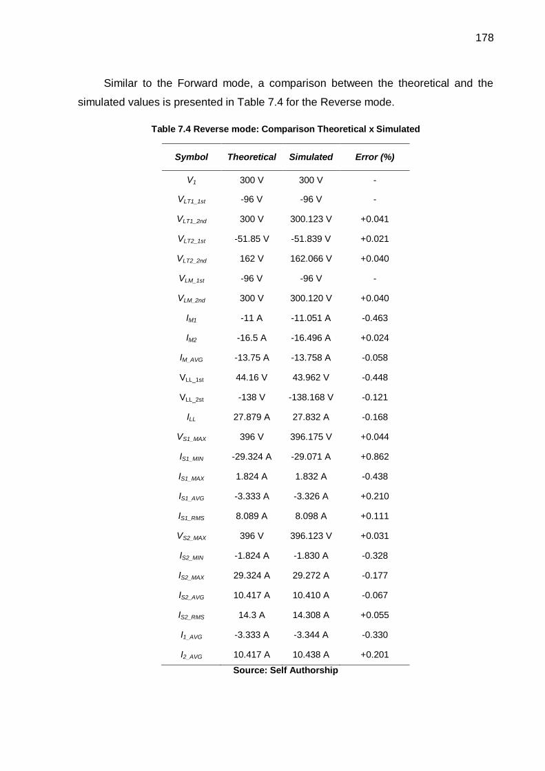
178
Similar to the Forward mode, a comparison between the theoretical and the
simulated values is presented in Table 7.4 for the Reverse mode.
Table 7.4 Reverse mode: Comparison Theoretical x Simulated
Symbol Theoretical Simulated Error (%)
V1 300 V 300 V -
VLT1_1st -96 V -96 V -
VLT1_2nd 300 V 300.123 V +0.041
VLT2_1st -51.85 V -51.839 V +0.021
VLT2_2nd 162 V 162.066 V +0.040
VLM_1st -96 V -96 V -
VLM_2nd 300 V 300.120 V +0.040
IM1 -11 A -11.051 A -0.463
IM2 -16.5 A -16.496 A +0.024
IM_AVG -13.75 A -13.758 A -0.058
VLL_1st 44.16 V 43.962 V -0.448
VLL_2st -138 V -138.168 V -0.121
ILL 27.879 A 27.832 A -0.168
VS1_MAX 396 V 396.175 V +0.044
IS1_MIN -29.324 A -29.071 A +0.862
IS1_MAX 1.824 A 1.832 A -0.438
IS1_AVG -3.333 A -3.326 A +0.210
IS1_RMS 8.089 A 8.098 A +0.111
VS2_MAX 396 V 396.123 V +0.031
IS2_MIN -1.824 A -1.830 A -0.328
IS2_MAX 29.324 A 29.272 A -0.177
IS2_AVG 10.417 A 10.410 A -0.067
IS2_RMS 14.3 A 14.308 A +0.055
I1_AVG -3.333 A -3.344 A -0.330
I2_AVG 10.417 A 10.438 A +0.201
Source: Self Authorship
179
7.4 CHAPTER CONCLUSION
In this chapter, the design methodology of the bidirectional ZVS Buck-Boost
DC-DC converter was presented. Also, in order to validate the theoretical analysis
from chapter 4, a digital simulation using the power electronics simulation software
PSIM® was performed.
Analyzing the simulation results presented in chapter 7 and the values provided
by Tables 7.3 and 7.4, it was possible to conclude that both theoretical steady state
analysis and simulations were performed correctly, since all the theoretical and
simulated values presented a high proximity, where the maximum error found was
1.033%, a value considered insignificant for engineering projects.
Also, with the ZVS operation the problem related to the reverse recovery
phenomenon of the antiparallel-body diodes from switches is solved and the
converter efficiency is increased, which is essential when thinking in an experimental
implementation.

180
CHAPTER 8
BIDIRECTIONAL DC-DC CONVERTER WITH TAPPED INDUCTOR:
EXPERIMENTAL RESULTS
8.1 CHAPTER INTRODUCTION
In this chapter, after all the knowledge provided by the previous chapters, the
experimental prototype of the bidirectional DC-DC converter with tapped inductor is
built. Then, experimental results for the 4 simulated modes in chapter 6 are
presented and discussed.
8.2 EXPERIMENTAL PROTOTYPE
With the values determined and verified by chapter 6, the choice of components
and the design of the tapped inductor may be done. Nevertheless, it is important to
highlight that as the converter can operate in different operating modes, the
requirements considered for the choice of components must attend the worst
scenario of the operations.
8.2.1 Choice of Components
For the choice of the switches to be used, the requirements considered were
their maximum voltage and the maximum current reached in steady state by any
point of the converter. As determined in chapter 6, the maximum voltage across the
switches is 396 V and the maximum current reached in the converter is 17.261 A.
Then, in a first moment, it was decided the use of the MOSFET SPW47N60C3 (650
V / 47 A).
However, after the first experimental tests, due to the high overvoltage in the
switches caused by the influence of the leakage inductance of the tapper inductor, it
was concluded to be unfeasible the use of the mentioned MOSFETs. Then, for

181
presenting a higher maximum voltage and a better antiparallel body-diode, the IGBT
IRGP20B120UD-EP (1200 V/ 40 A) was implemented in the experimental prototype.
Also, three 10 kΩ/ 0.25 W resistors were used as gate resistor for the switches,
and for their driving system 2 drivers from the company Supplier were selected: one
double isolated driver (Supplier DRO100D25A) and one simple isolated driver
(Supplier DRO100S25A).
About the decoupling capacitors C1 and C2, because of the reliability and
extended lifetime of polypropylene capacitors, two 40 µF/450 V polypropylene
capacitors were used.
For the current sensor, the sensor LEM LA 25-NP was selected, mainly
because of its reliability, accuracy and good linearity, factors that facilitate an
experimental implementation.
8.2.2 Tapped Inductor Design
In Table 8.1, the constructive aspects of the tapped inductor are presented. All
the design methodology of the tapped inductor may be seen in the Appendix D.
Table 8.1 Constructive aspects of the Tapped inductor
Component Specification
Tapped inductor
Magnetizing Inductance: LM = 513.711 µH Turns in the primary: 29
Turns in the secondary: 29 Wire in the primary: 23 x 25 AWG
Wire in the secondary: 10 x 25 AWG Core: EE-76 Thornton IP12R
Source: Self Authorship
8.2.3 RCD Clamping
One of the recurring issues in power converters implementing tapped inductors
and transformers is the influence of the leakage inductance in the system. When in
series with switches, these inductances can cause even the destruction of the power
elements.
182
This happens because the leakage inductance accumulates energy during the
time period where the switch in turned-on, and when this switch is turned-off the
current on this inductance is abruptly interrupted and the energy is consequently
suddenly discharged, resulting in an overvoltage to the switches.
In order to remedy that, clamping circuits are commonly implemented. The idea
behind clamping circuits is to provide an alternative path for the leakage inductance
energy when the switch is turned-off, preventing the overvoltage effect and the
destruction of the power switches. In Figure 8.1, the two classical clamping circuits
are presented.
Dc
Cc CcRc
Sc
(a) (b)
Figure 8.1 Clamping circuits: (a) Passive clamping (b) Active clamping
Source: Self Authorship
In this work, it was determined the use of the passive clamping circuit for each
switch, mainly because the implementation of an active clamping would lead to a
very complex circuit and the addition of 3 more switches would counter one of the
main appeals of the converter, the use of the tapped inductor for reducing switches
from the original topology.
In the passive clamping, the energy from the leakage inductance is transferred
to the clamping capacitor Cc by the clamping diode Dc, and it is completely dissipated
in the clamping resistor Rc.
Then, assuming the specifications determined earlier in this chapter, the
components of the clamping circuit may be determined. As all the switches
implemented are the same and are under very close conditions, the same elements
were used in all 3 switches.

183
First, the clamping diode must attend the same voltage parameter than the
switch selected. As the switch chosen presents a maximum voltage of 1200 V, for
presenting a close value of maximum voltage, it was chosen the diode MUR 1100
(1000 V/ 1 A) for the clamping circuit.
The clamping capacitors were selected to support the maximum voltage of the
clamping circuit with a very small ripple. For this, due to the availability of
components in the UTFPR-PG Research Center and after some initial tests using
arbitrary capacitances, it was determined the use of two 470 nF/ 400 V polyester
capacitors in series as the best choice in terms of operation.
Finally, it is function of the clamping resistor to limit the clamping voltage and
reduce the dissipated power by the clamping circuit. Then, to determine the value of
this resistor, tests were performed to find the resistance which would combine the
best relationship between converter performance and clamping voltage. After that,
the use of two 56 kΩ / 3 W resistance in series for each switch proved to be the best
solution for the converter operation.
Then, all the components determined in this section and implemented in the
prototype are summarized in Table 8.2.
Table 8.2 Components used in the prototype
Component Specification
Switches S1, S2 and S3 3 x IRGP20B120UD-EP (1200 V/ 40 A)
Decoupling capacitors C1 and C2 2 x Polypropylene 40 µF / 450 V
Clamping capacitors 6 x 470 nF / 400 V
(3 x 235 nF / 800 V)
Clamping diodes 3 x MUR 1100 (1000 V/ 1 A)
Clamping resistors 6 x 56 kΩ / 3W
(3 x 112 kΩ / 6W )
Current sensor LEM LA 25-NP
Gate resistors 3 x 10 kΩ / 0.25 W
Drivers 1 x Supplier DRO100D25A 1 x Supplier DRO100S25A
Source: Self Authorship
Following, the experimental prototype is presented in Figure 8.2 whereas the
tapped inductor is shown by Figure 8.3.

184
16.75 cm16 c
m
Figure 8.2 Experimental prototype
Source: Self Authorship
7.5 cm7.
5 cm
Figure 8.3 Tapped inductor
Source: Self Authorship
185
8.3 EXPERIMENTAL SETUP
Due to the lack of a battery bank and SCs or any bidirectional DC power source
in the UTFPR-PG Research Center, the experimental tests were performed with the
converter working unidirectionally, that is, with a DC power source supplying a RC
load.
When the converter is tested operating in the Forward mode, the DC power
source is placed as the voltage source V1 and the RC load is placed as the voltage
source V2. Already for the Reverse mode, the opposite is done, the DC power source
is placed as the voltage source V2 and the RC load is placed as the voltage source
V1.
Following, all the elements used in the experimental setup implemented in
laboratory are described:
The Bidirectional DC-DC converter with tapped inductor;
1 DSP Texas Instruments TMS320F28335 Experimenter Kit : Used for the
control of the converter;
1 Voltage gain circuit: Implemented to adapt the gate signals for the switches
from the DSP level (3.3 V) to the Drivers level (15 V) (Schematic and PCB
layout available in the Appendix E);
1 Signal treatment circuit: Implemented to adapt the power measurements to
DSP level signals (Schematic and PCB layout available in the Appendix F);
1 Supplier DC Power Source: to supply the converter as one of the voltage
sources;
1 parallel RC load: Used to emulate the remaining voltage source, where the
value of the resistance is adjusted according the desired power and the
capacitance is a capacitor bank of 2.82 mF / 400 V.
1 Digital Phosphor Oscilloscope Tektronix DPO7254C: Used to obtain all the
waveforms from the experimental prototype;
1 Power Analyzer Yokogawa WT500: Used to obtain all the efficiency results
from the experimental prototype;
This way, a schematic of the experimental setup implemented in laboratory is
presented in Figure 8.4.

186
DSPDC-DC
CONVERTER
OPEN LOOP
CLOSED LOOP
SIGNAL
TREATMENT
15V
PWM SIGNAL
3.3V
PWM SIGNAL
VOLTAGE
GAIN
V1
V2
I1
Figure 8.4 Schematic of the experimental setup
Source: Self Authorship
8.4 EXPERIMENTAL RESULTS
In this section, all the closed loop experimental results of the bidirectional DC-
DC converter with tapped inductor are going to be presented.
8.4.1 Forward Buck
First, the gate signals for the Forward Buck are presented in Figure 8.5.
t = 20 µs/div
VgS2
VgS3
VgS1
Figure 8.5 Forward Buck: Gate signals (10 V/div)
Source: Self Authorship
187
As can be seen in Figure 8.5, switches S1 and S3 are receiving complementary
PWM signals with amplitude of 15 V whereas the switch S2 is receiving a continuous
15 V signal. This configuration of signals is important to guarantee, when the
converter is operating bidirectionally, the possibility of the direct change from the
Forward to the Reverse mode (and vice versa) just changing the current reference.
Then, in Figures 8.6 and 8.7, the voltage and the current in switch S1 are
presented, where the maximum voltage reached in this switch was 543.2 V and the
RMS value of the current was 4.862 A. However, after the initial voltage spike, it is
possible to see that the voltage across this switch stabilizes in approximately 400 V.
t = 20 µs/div
VS1
IS1
Figure 8.6 Forward Buck: Voltage (200 V/div) and current (7 A/div) in the switch S1
Source: Self Authorship
t = 20 µs/div
VS1
IS1
Figure 8.7 Forward Buck: Voltage (200 V/div) and current (7 A/div) in the switch S1
Source: Self Authorship
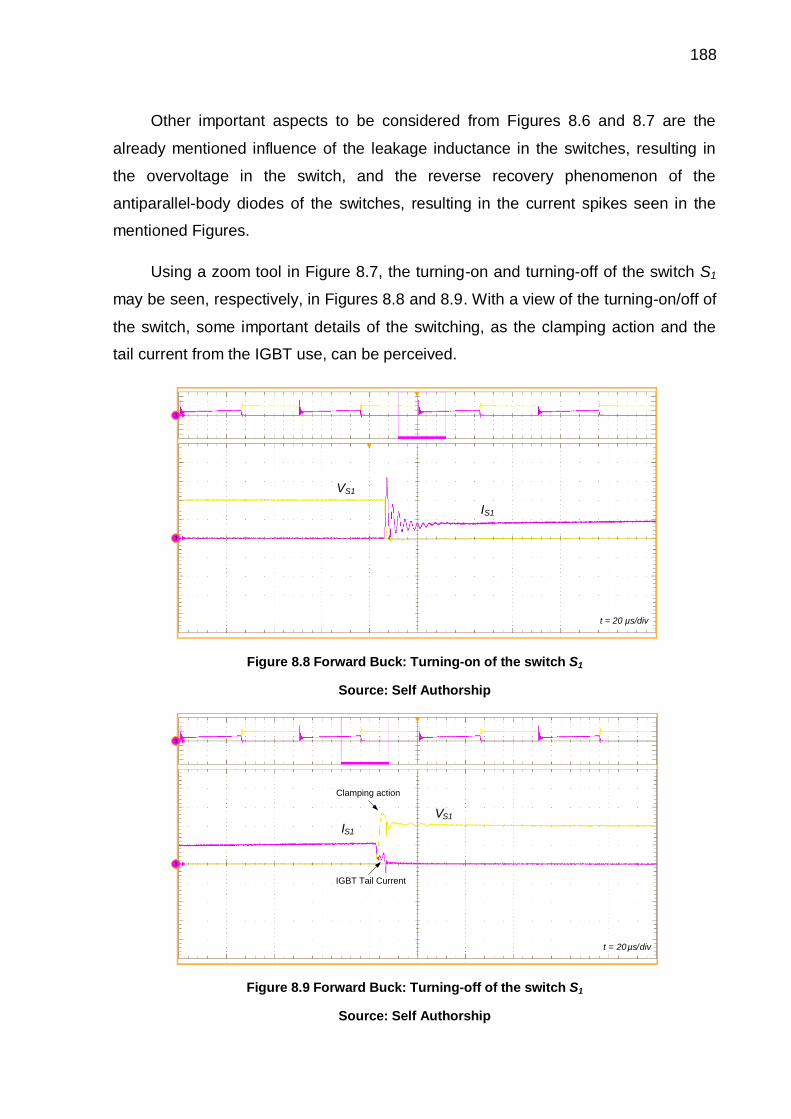
188
Other important aspects to be considered from Figures 8.6 and 8.7 are the
already mentioned influence of the leakage inductance in the switches, resulting in
the overvoltage in the switch, and the reverse recovery phenomenon of the
antiparallel-body diodes of the switches, resulting in the current spikes seen in the
mentioned Figures.
Using a zoom tool in Figure 8.7, the turning-on and turning-off of the switch S1
may be seen, respectively, in Figures 8.8 and 8.9. With a view of the turning-on/off of
the switch, some important details of the switching, as the clamping action and the
tail current from the IGBT use, can be perceived.
t = 20 µs/div
VS1
IS1
Figure 8.8 Forward Buck: Turning-on of the switch S1
Source: Self Authorship
t = 20 µs/div
VS1
IS1
Clamping action
IGBT Tail Current
Figure 8.9 Forward Buck: Turning-off of the switch S1
Source: Self Authorship
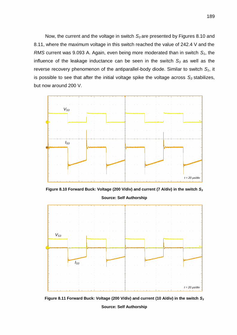
189
Now, the current and the voltage in switch S3 are presented by Figures 8.10 and
8.11, where the maximum voltage in this switch reached the value of 242.4 V and the
RMS current was 9.093 A. Again, even being more moderated than in switch S1, the
influence of the leakage inductance can be seen in the switch S3 as well as the
reverse recovery phenomenon of the antiparallel-body diode. Similar to switch S1, it
is possible to see that after the initial voltage spike the voltage across S3 stabilizes,
but now around 200 V.
t = 20 µs/div
IS3
VS3
Figure 8.10 Forward Buck: Voltage (200 V/div) and current (7 A/div) in the switch S3
Source: Self Authorship
t = 20 µs/div
VS3
IS3
Figure 8.11 Forward Buck: Voltage (200 V/div) and current (10 A/div) in the switch S3
Source: Self Authorship

190
Then, in the same way as for the switch S1, the turning-on and the turning-off of
the switch S3 can be seen with a zoom in Figure 8.11 and are presented,
respectively, by Figures 8.12 and 8.13.
t = 20 µs/div
VS3
IS3
Figure 8.12 Forward Buck: Turning-on of the switch S3
Source: Self Authorship
t = 20 µs/div
VS3
IS3
Figure 8.13 Forward Buck: Turning-off of the switch S3
Source: Self Authorship
In Figures 8.14 and 8.15, the voltage and current waveforms in the voltage
sources are presented. In the voltage source 1, the average current was 3.344 A
whereas in the voltage source 2 this value was -9.635 A. About the voltage in each
voltage source, both presented the expected values, 300 V in V1 and 96 V in V2.
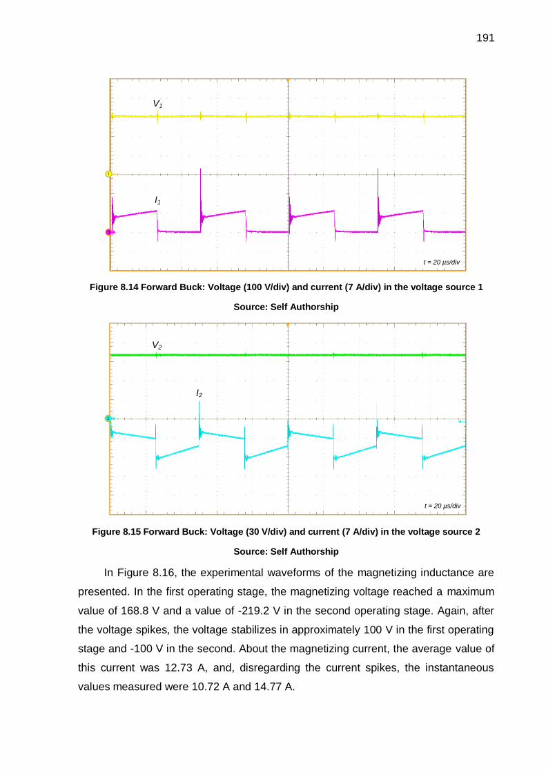
191
t = 20 µs/div
V1
I1
Figure 8.14 Forward Buck: Voltage (100 V/div) and current (7 A/div) in the voltage source 1
Source: Self Authorship
t = 20 µs/div
V2
I2
Figure 8.15 Forward Buck: Voltage (30 V/div) and current (7 A/div) in the voltage source 2
Source: Self Authorship
In Figure 8.16, the experimental waveforms of the magnetizing inductance are
presented. In the first operating stage, the magnetizing voltage reached a maximum
value of 168.8 V and a value of -219.2 V in the second operating stage. Again, after
the voltage spikes, the voltage stabilizes in approximately 100 V in the first operating
stage and -100 V in the second. About the magnetizing current, the average value of
this current was 12.73 A, and, disregarding the current spikes, the instantaneous
values measured were 10.72 A and 14.77 A.
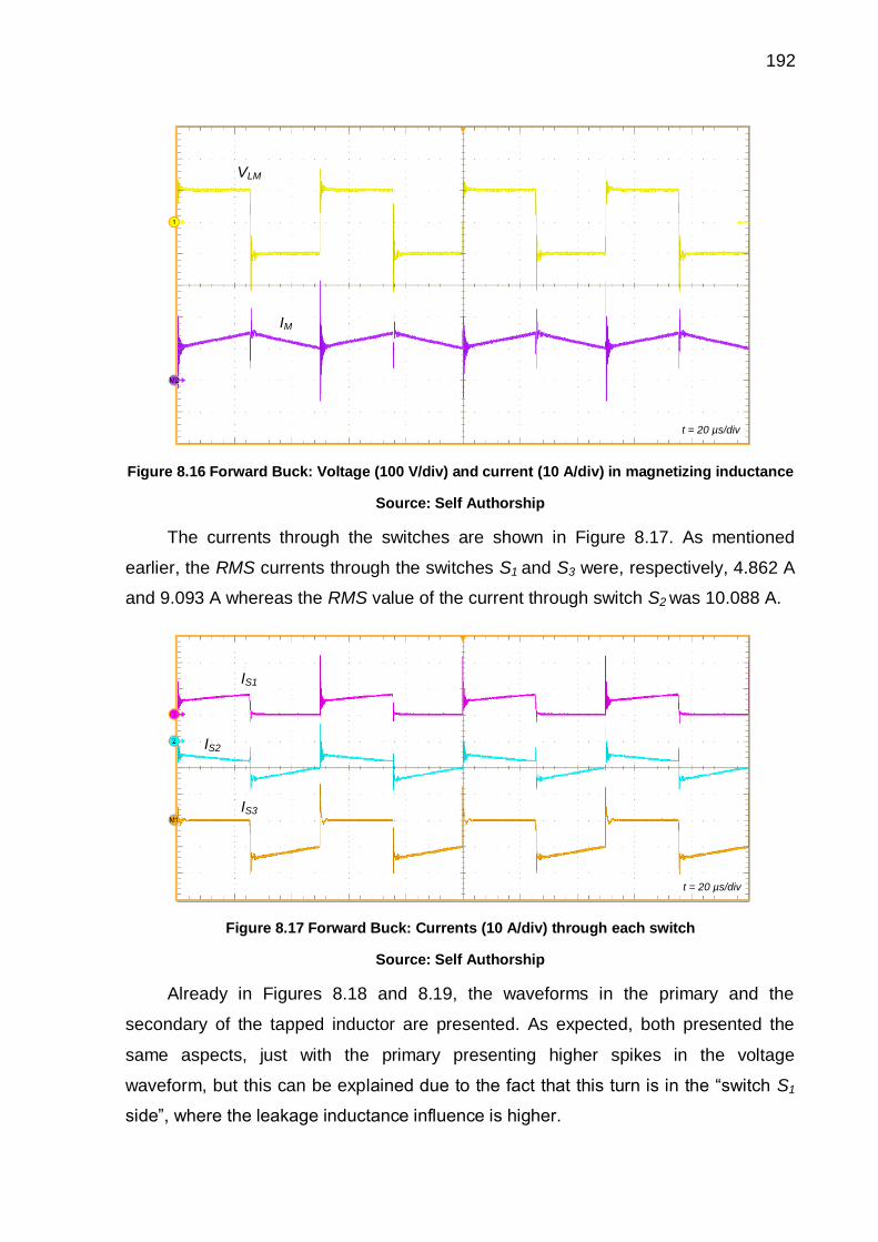
192
t = 20 µs/div
VLM
IM
Figure 8.16 Forward Buck: Voltage (100 V/div) and current (10 A/div) in magnetizing inductance
Source: Self Authorship
The currents through the switches are shown in Figure 8.17. As mentioned
earlier, the RMS currents through the switches S1 and S3 were, respectively, 4.862 A
and 9.093 A whereas the RMS value of the current through switch S2 was 10.088 A.
t = 20 µs/div
IS1
IS2
IS3
Figure 8.17 Forward Buck: Currents (10 A/div) through each switch
Source: Self Authorship
Already in Figures 8.18 and 8.19, the waveforms in the primary and the
secondary of the tapped inductor are presented. As expected, both presented the
same aspects, just with the primary presenting higher spikes in the voltage
waveform, but this can be explained due to the fact that this turn is in the “switch S1
side”, where the leakage inductance influence is higher.

193
t = 20 µs/div
VLT1
ILT1
Figure 8.18 Forward Buck: Voltage (100 V/div) and current (7 A/div) in the primary
Source: Self Authorship
t = 20 µs/div
VLT2
ILT2
Figure 8.19 Forward Buck: Voltage (100 V/div) and current (7 A/div) in the secondary
Source: Self Authorship
Then, the current control action of the system is presented in Figure 8.20. As
well as in the simulations made in chapter 6, the control was tested with a step from
50% to 100% of the rated power (1.667 A – 3.335 A) in the current reference. As can
be seen in 8.20, the control worked well, where the current provided by the DC power
source changed properly with the reference steps, with no variations in the voltage
V1. Another important aspect to be seen in Figure 8.21 is that, even without the use
of a filter in the input, just using the decoupling capacitor C1 and the inductance of the
wires used in the experimental setup, that is, just with the experimental setup
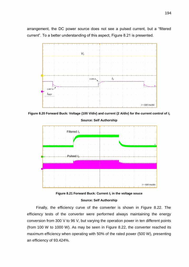
194
arrangement, the DC power source does not see a pulsed current, but a “filtered
current”. To a better understanding of this aspect, Figure 8.21 is presented.
t = 500 ms/div
V1
I1
1.667 A
3.335 A
IREF
Figure 8.20 Forward Buck: Voltage (100 V/div) and current (2 A/div) for the current control of I1
Source: Self Authorship
Filtered I1
t = 500 ms/div
Pulsed I1
Figure 8.21 Forward Buck: Current I1 in the voltage souce
Source: Self Authorship
Finally, the efficiency curve of the converter is shown in Figure 8.22. The
efficiency tests of the converter were performed always maintaining the energy
conversion from 300 V to 96 V, but varying the operation power in ten different points
(from 100 W to 1000 W). As may be seen in Figure 8.22, the converter reached its
maximum efficiency when operating with 50% of the rated power (500 W), presenting
an efficiency of 93.424%.

195
50 150 250 350 450 550 650 750 850 950 1050
90.25
90.75
91.25
91.75
92.25
92.75
93.25
93.75
Power (W)
Effic
ien
cy (
%)
Figure 8.22 Forward Buck: Efficiency curve
Source: Self Authorship
With the experimental results of the Forward Buck presented, a comparison
with the theoretical and simulated values is proposed in Table 8.3.
Table 8.3 Forward Buck: Comparison Theoretical x Simulated x Experimental
Symbol Theoretical Simulated Experimental
Stabilized Value Peak Value
VS1_MAX 396 V 396 V 400 V 543.2 V
VS3_MAX 198 V 198 V 200 V 242.4 V
VLT1_1st 102 V 102 V 100 V 170.8 V
VLT1_2nd -96 V -96 V -100 V -221.6 V
VLT2_1st 102 V 102 V 100 V 156.8 V
VLT2_2nd -96 V -96 V -100 V -135.6 V
VLM_1st 102 V 102 V 100 V 168.8 V
VLM_2nd -96 V -96 V -100 V -219.2 V
IM1 11.343 A 11.334 A 10.72 A
IM2 16.157 A 16.148 A 14.77 A
IM_AVG 13.75 A 13.743 A 12.73 A
I1_AVG 3.333 A 3.327 A 3.344 A
I2_AVG -10.417 A -10.415 A -9.635 A
IS1_RMS 4.812 A 4.783 A 4.862 A
IS2_RMS 11.024 A 11.052 A 10.088 A
IS3_RMS 9.919 A 9.962 A 9.093 A
Source: Self Authorship
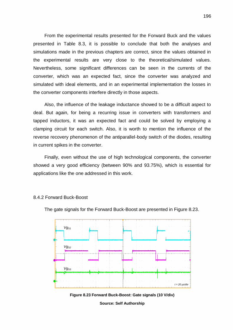
196
From the experimental results presented for the Forward Buck and the values
presented in Table 8.3, it is possible to conclude that both the analyses and
simulations made in the previous chapters are correct, since the values obtained in
the experimental results are very close to the theoretical/simulated values.
Nevertheless, some significant differences can be seen in the currents of the
converter, which was an expected fact, since the converter was analyzed and
simulated with ideal elements, and in an experimental implementation the losses in
the converter components interfere directly in those aspects.
Also, the influence of the leakage inductance showed to be a difficult aspect to
deal. But again, for being a recurring issue in converters with transformers and
tapped inductors, it was an expected fact and could be solved by employing a
clamping circuit for each switch. Also, it is worth to mention the influence of the
reverse recovery phenomenon of the antiparallel-body switch of the diodes, resulting
in current spikes in the converter.
Finally, even without the use of high technological components, the converter
showed a very good efficiency (between 90% and 93.75%), which is essential for
applications like the one addressed in this work.
8.4.2 Forward Buck-Boost
The gate signals for the Forward Buck-Boost are presented in Figure 8.23.
VgS1
t = 20 µs/div
VgS2
VgS3
Figure 8.23 Forward Buck-Boost: Gate signals (10 V/div)
Source: Self Authorship
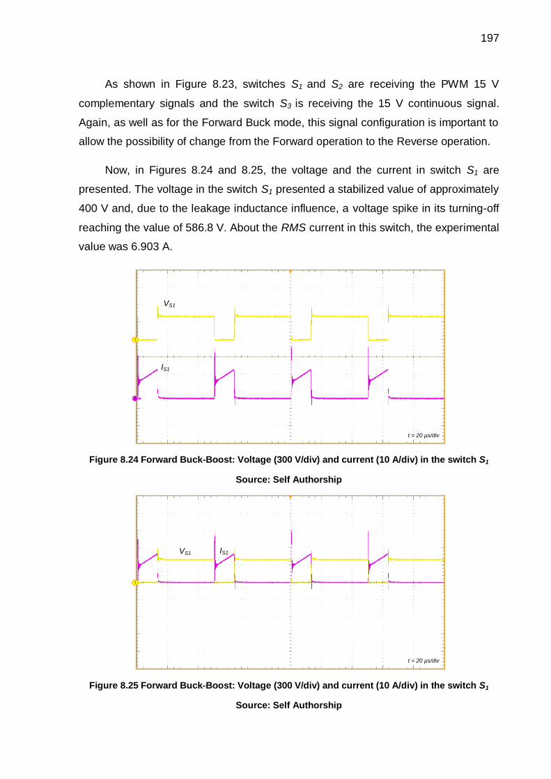
197
As shown in Figure 8.23, switches S1 and S2 are receiving the PWM 15 V
complementary signals and the switch S3 is receiving the 15 V continuous signal.
Again, as well as for the Forward Buck mode, this signal configuration is important to
allow the possibility of change from the Forward operation to the Reverse operation.
Now, in Figures 8.24 and 8.25, the voltage and the current in switch S1 are
presented. The voltage in the switch S1 presented a stabilized value of approximately
400 V and, due to the leakage inductance influence, a voltage spike in its turning-off
reaching the value of 586.8 V. About the RMS current in this switch, the experimental
value was 6.903 A.
t = 20 µs/div
VS1
IS1
Figure 8.24 Forward Buck-Boost: Voltage (300 V/div) and current (10 A/div) in the switch S1
Source: Self Authorship
t = 20 µs/div
VS1 IS1
Figure 8.25 Forward Buck-Boost: Voltage (300 V/div) and current (10 A/div) in the switch S1
Source: Self Authorship
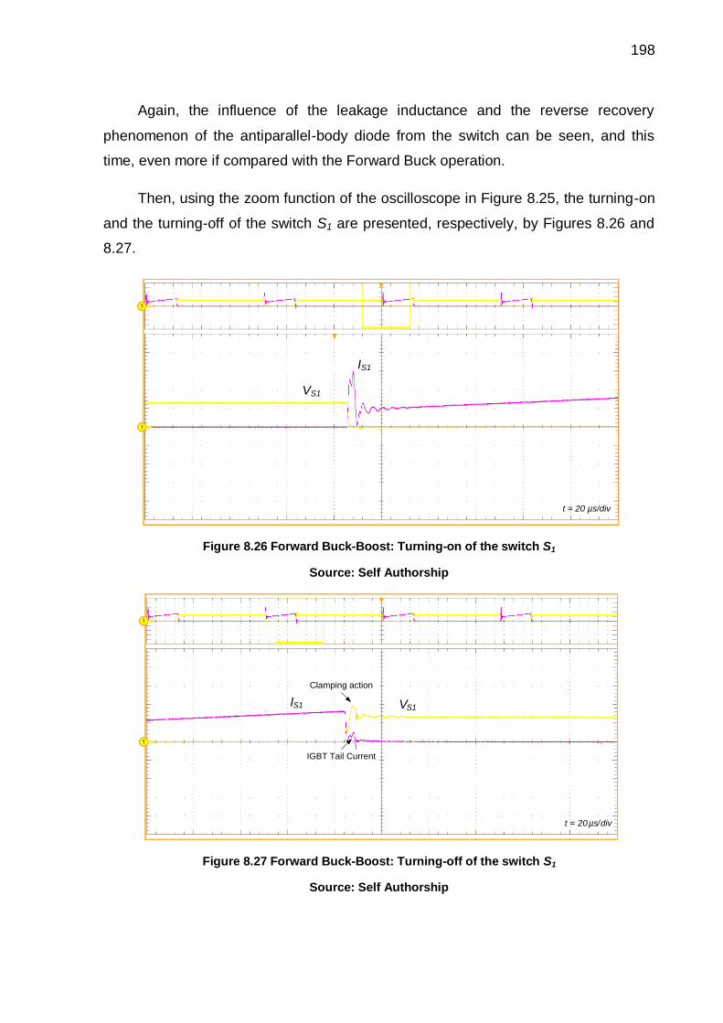
198
Again, the influence of the leakage inductance and the reverse recovery
phenomenon of the antiparallel-body diode from the switch can be seen, and this
time, even more if compared with the Forward Buck operation.
Then, using the zoom function of the oscilloscope in Figure 8.25, the turning-on
and the turning-off of the switch S1 are presented, respectively, by Figures 8.26 and
8.27.
t = 20 µs/div
VS1
IS1
Figure 8.26 Forward Buck-Boost: Turning-on of the switch S1
Source: Self Authorship
IGBT Tail Current
t = 20 µs/div
VS1IS1
Clamping action
Figure 8.27 Forward Buck-Boost: Turning-off of the switch S1
Source: Self Authorship
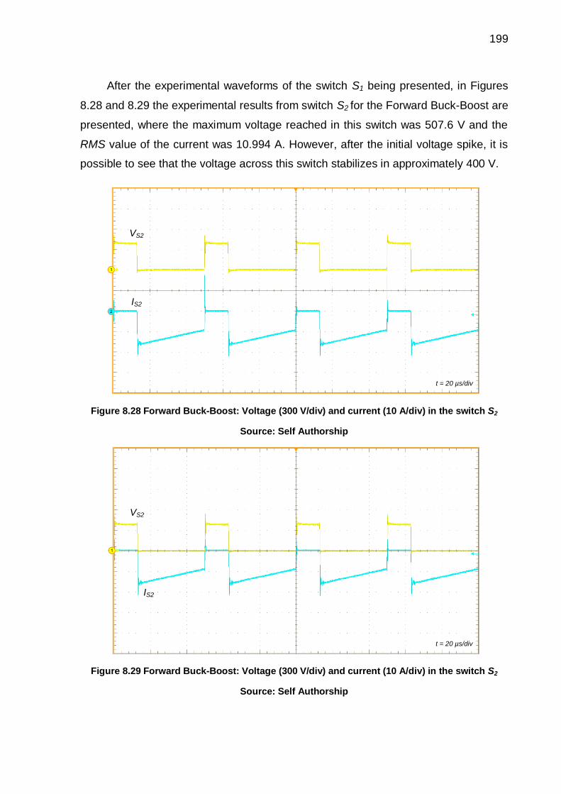
199
After the experimental waveforms of the switch S1 being presented, in Figures
8.28 and 8.29 the experimental results from switch S2 for the Forward Buck-Boost are
presented, where the maximum voltage reached in this switch was 507.6 V and the
RMS value of the current was 10.994 A. However, after the initial voltage spike, it is
possible to see that the voltage across this switch stabilizes in approximately 400 V.
t = 20 µs/div
VS2
IS2
Figure 8.28 Forward Buck-Boost: Voltage (300 V/div) and current (10 A/div) in the switch S2
Source: Self Authorship
t = 20 µs/div
VS2
IS2
Figure 8.29 Forward Buck-Boost: Voltage (300 V/div) and current (10 A/div) in the switch S2
Source: Self Authorship

200
In the same way as the switch S1, using the zoom function of the oscilloscope in
Figure 8.29, the turning-on of the switch S2 is presented by Figure 8.30 whereas the
turning-off is shown in Figure 8.31.
t = 20 µs/div
VS2
IS2
Figure 8.30 Forward Buck-Boost: Turning-on of the switch S2
Source: Self Authorship
t = 20 µs/div
VS2
IS2
Clamping action
IGBT Tail Current
Figure 8.31 Forward Buck-Boost: Turning-off of the switch S2
Source: Self Authorship
In Figures 8.32 and 8.33, the voltage and current waveforms in the voltage
sources are presented. In the voltage source 1, the average current was 3.362 A
whereas in the voltage source 2 this value was -9.249 A. About the voltage in each
voltage source, both presented the expected values, 300 V in V1 and 96 V in V2.

201
V1
I1
t = 20 µs/div
Figure 8.32 Forward Buck-Boost: Voltage (100 V/div) and current (10 A/div) in V1
Source: Self Authorship
t = 20 µs/div
V2
I2
Figure 8.33 Forward Buck-Boost: Voltage (30 V/div) and current (10 A/div) in V2
Source: Self Authorship
The experimental waveforms of the magnetizing inductance are presented in
Figure 8.34. In the first operating stage, the magnetizing voltage presented a
stabilized value around 300 V and -100 V in the second. However, considering the
voltage spikes in the magnetizing voltage, the maximum value reached was 365.6 V
and the minimum was -300 V. About the magnetizing current, the average value of
this current was 12.51 A, and, disregarding the current spikes, the instantaneous
values measured were 9.889 A and 16.147 A.

202
t = 20 µs/div
VLM
IM
Figure 8.34 Forward Buck-Boost: Voltage (200 V/div) and current (10 A/div) in the magnetizing inductance
Source: Self Authorship
Then, in Figure 8.35 the currents through the switches are shown. The switches
S1, S2 and S3 presented, respectively, the RMS values of 6.903 A, 10.994 A and
12.324 A.
t = 20 µs/div
IS1
IS2
IS3
Figure 8.35 Forward Buck-Boost: Currents (20 A/div) through each switch
Source: Self Authorship
In Figures 8.36 and 8.37, the waveforms in each turn of the tapped inductor are
presented. Again, due to the turn ratio n=1, the waveforms presented the same
aspects, presenting a stabilized value of 300 V in the first operating stage and -100 V
in the second. About the voltage spikes, the maximum value reached was 420 V and
the minimum -300.8 V.

203
t = 20 µs/div
VLT1
ILT1
Figure 8.36 Forward Buck-Boost: Voltage (200 V/div) and current (10 A/div) in the primary
Source: Self Authorship
t = 20 µs/div
VLT2
ILT2
Figure 8.37 Forward Buck-Boost: Voltage (200 V/div) and current (10 A/div) in the primary
Source: Self Authorship
The experimental results of the control for the Forward Buck-Boost are
presented by Figure 8.38. The control tests were performed with the same
methodology of the Forward Buck, applying steps in the current I1 reference and
checking its behavior after that. Again, the control showed to be working well and, as
well as the Forward Buck, the experimental setup arrangement worked as a filter for
the current seen by the DC power source. Nevertheless, it is important to highlight
that as this feature of the experimental setup was already presented in Figure 8.21, it
will not be presented again for the next operating modes.
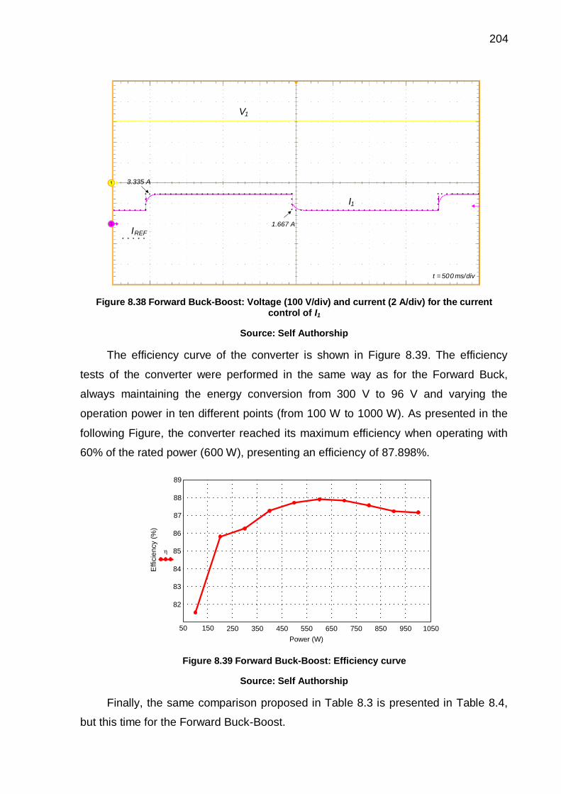
204
t = 500 ms/div
V1
I1
IREF
1.667 A
3.335 A
Figure 8.38 Forward Buck-Boost: Voltage (100 V/div) and current (2 A/div) for the current control of I1
Source: Self Authorship
The efficiency curve of the converter is shown in Figure 8.39. The efficiency
tests of the converter were performed in the same way as for the Forward Buck,
always maintaining the energy conversion from 300 V to 96 V and varying the
operation power in ten different points (from 100 W to 1000 W). As presented in the
following Figure, the converter reached its maximum efficiency when operating with
60% of the rated power (600 W), presenting an efficiency of 87.898%.
50 150 250 350 450 550 650 750 850 950 1050
82
83
84
85
86
87
88
89
Power (W)
Effic
ien
cy (
%)
Figure 8.39 Forward Buck-Boost: Efficiency curve
Source: Self Authorship
Finally, the same comparison proposed in Table 8.3 is presented in Table 8.4,
but this time for the Forward Buck-Boost.
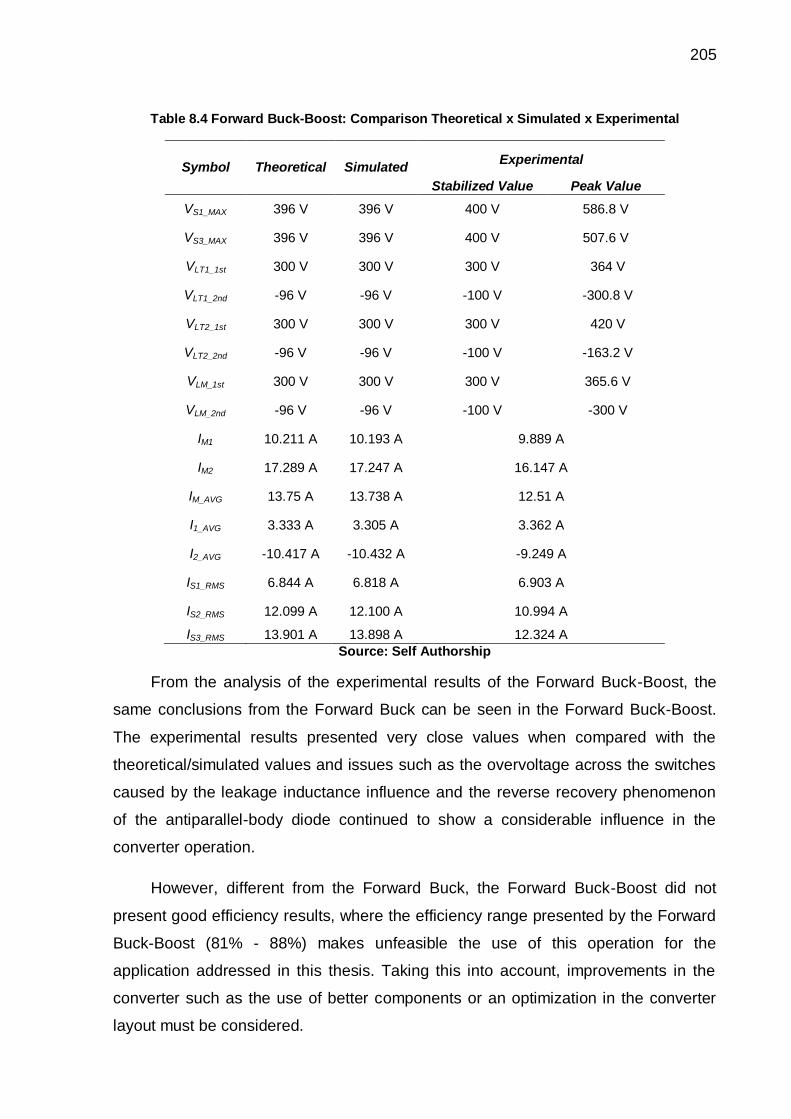
205
Table 8.4 Forward Buck-Boost: Comparison Theoretical x Simulated x Experimental
Symbol Theoretical Simulated Experimental
Stabilized Value Peak Value
VS1_MAX 396 V 396 V 400 V 586.8 V
VS3_MAX 396 V 396 V 400 V 507.6 V
VLT1_1st 300 V 300 V 300 V 364 V
VLT1_2nd -96 V -96 V -100 V -300.8 V
VLT2_1st 300 V 300 V 300 V 420 V
VLT2_2nd -96 V -96 V -100 V -163.2 V
VLM_1st 300 V 300 V 300 V 365.6 V
VLM_2nd -96 V -96 V -100 V -300 V
IM1 10.211 A 10.193 A 9.889 A
IM2 17.289 A 17.247 A 16.147 A
IM_AVG 13.75 A 13.738 A 12.51 A
I1_AVG 3.333 A 3.305 A 3.362 A
I2_AVG -10.417 A -10.432 A -9.249 A
IS1_RMS 6.844 A 6.818 A 6.903 A
IS2_RMS 12.099 A 12.100 A 10.994 A
IS3_RMS 13.901 A 13.898 A 12.324 A
Source: Self Authorship
From the analysis of the experimental results of the Forward Buck-Boost, the
same conclusions from the Forward Buck can be seen in the Forward Buck-Boost.
The experimental results presented very close values when compared with the
theoretical/simulated values and issues such as the overvoltage across the switches
caused by the leakage inductance influence and the reverse recovery phenomenon
of the antiparallel-body diode continued to show a considerable influence in the
converter operation.
However, different from the Forward Buck, the Forward Buck-Boost did not
present good efficiency results, where the efficiency range presented by the Forward
Buck-Boost (81% - 88%) makes unfeasible the use of this operation for the
application addressed in this thesis. Taking this into account, improvements in the
converter such as the use of better components or an optimization in the converter
layout must be considered.
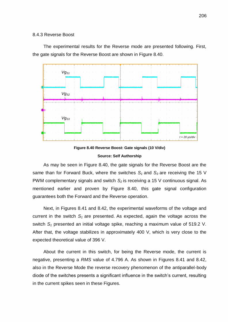
206
8.4.3 Reverse Boost
The experimental results for the Reverse mode are presented following. First,
the gate signals for the Reverse Boost are shown in Figure 8.40.
t = 20 µs/div
VgS1
VgS3
VgS2
Figure 8.40 Reverse Boost: Gate signals (10 V/div)
Source: Self Authorship
As may be seen in Figure 8.40, the gate signals for the Reverse Boost are the
same than for Forward Buck, where the switches S1 and S3 are receiving the 15 V
PWM complementary signals and switch S2 is receiving a 15 V continuous signal. As
mentioned earlier and proven by Figure 8.40, this gate signal configuration
guarantees both the Forward and the Reverse operation.
Next, in Figures 8.41 and 8.42, the experimental waveforms of the voltage and
current in the switch S1 are presented. As expected, again the voltage across the
switch S1 presented an initial voltage spike, reaching a maximum value of 519.2 V.
After that, the voltage stabilizes in approximately 400 V, which is very close to the
expected theoretical value of 396 V.
About the current in this switch, for being the Reverse mode, the current is
negative, presenting a RMS value of 4.796 A. As shown in Figures 8.41 and 8.42,
also in the Reverse Mode the reverse recovery phenomenon of the antiparallel-body
diode of the switches presents a significant influence in the switch’s current, resulting
in the current spikes seen in these Figures.
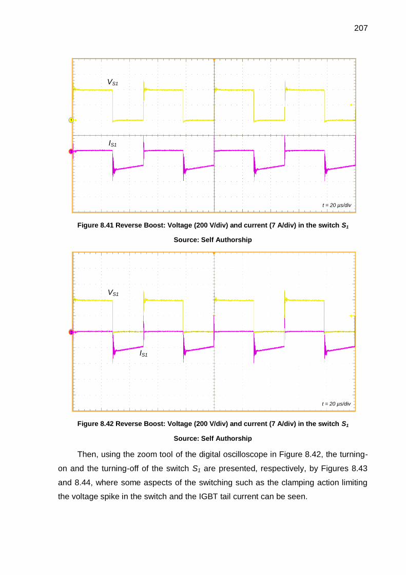
207
t = 20 µs/div
VS1
IS1
Figure 8.41 Reverse Boost: Voltage (200 V/div) and current (7 A/div) in the switch S1
Source: Self Authorship
t = 20 µs/div
VS1
IS1
Figure 8.42 Reverse Boost: Voltage (200 V/div) and current (7 A/div) in the switch S1
Source: Self Authorship
Then, using the zoom tool of the digital oscilloscope in Figure 8.42, the turning-
on and the turning-off of the switch S1 are presented, respectively, by Figures 8.43
and 8.44, where some aspects of the switching such as the clamping action limiting
the voltage spike in the switch and the IGBT tail current can be seen.

208
t = 20 µs/div
VS1
IS1
Figure 8.43 Reverse Boost: Turning-on of the switch S1
Source: Self Authorship
t = 20 µs/div
IS1
VS1
Clamping Action
IGBT Tail Current
Figure 8.44 Reverse Boost: Turning-off of the switch S1
Source: Self Authorship
Now, the current and the voltage in switch S3 are presented by Figures 8.45
and 8.46, where the voltage in this switch presented a stabilized value of
approximately 200 V, with a peak value of 221.6 V.
About the current in this switch, the experimental RMS value measured was
10.933 A.
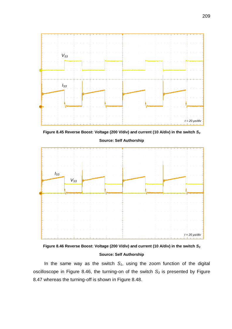
209
t = 20 µs/div
VS3
IS3
Figure 8.45 Reverse Boost: Voltage (200 V/div) and current (10 A/div) in the switch S3
Source: Self Authorship
t = 20 µs/div
VS3
IS3
Figure 8.46 Reverse Boost: Voltage (200 V/div) and current (10 A/div) in the switch S3
Source: Self Authorship
In the same way as the switch S1, using the zoom function of the digital
oscilloscope in Figure 8.46, the turning-on of the switch S3 is presented by Figure
8.47 whereas the turning-off is shown in Figure 8.48.
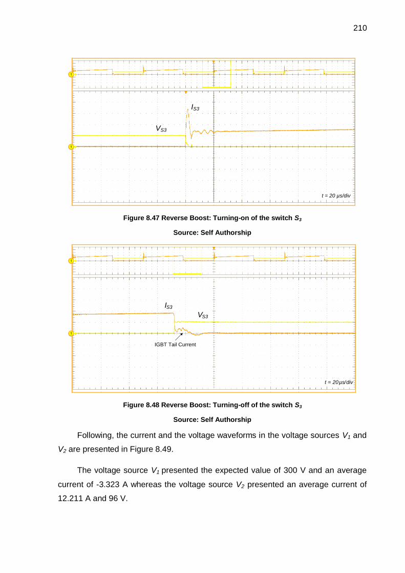
210
t = 20 µs/div
VS3
IS3
Figure 8.47 Reverse Boost: Turning-on of the switch S3
Source: Self Authorship
t = 20 µs/div
VS3
IS3
IGBT Tail Current
Figure 8.48 Reverse Boost: Turning-off of the switch S3
Source: Self Authorship
Following, the current and the voltage waveforms in the voltage sources V1 and
V2 are presented in Figure 8.49.
The voltage source V1 presented the expected value of 300 V and an average
current of -3.323 A whereas the voltage source V2 presented an average current of
12.211 A and 96 V.

211
t = 20 µs/div
V1
V2
I1
I2
Figure 8.49 Reverse Boost: Voltage (100 V/div) and current (10 A/div) in the voltage sources V1 and V2
Source: Self Authorship
In Figure 8.50, the experimental waveforms of the magnetizing inductance for
the Reverse Boost are presented. In the first operating stage, the magnetizing
voltage reached a value of -226.4 V and a value of 208.4 V in the second operating
stage. Again, after the initial voltage spikes, the voltage stabilizes in approximately -
100 V in the first operating stage and 100 V in the second. About the magnetizing
current, the average value of this current was -14.352 A, and, disregarding the
current spikes, the instantaneous values measured were -17.872 A and -11.936 A.
t = 20 µs/div
IM
VLM
Figure 8.50 Reverse Boost: Voltage (100 V/div) and current (10 A/div) in the magnetizing inductance
Source: Self Authorship
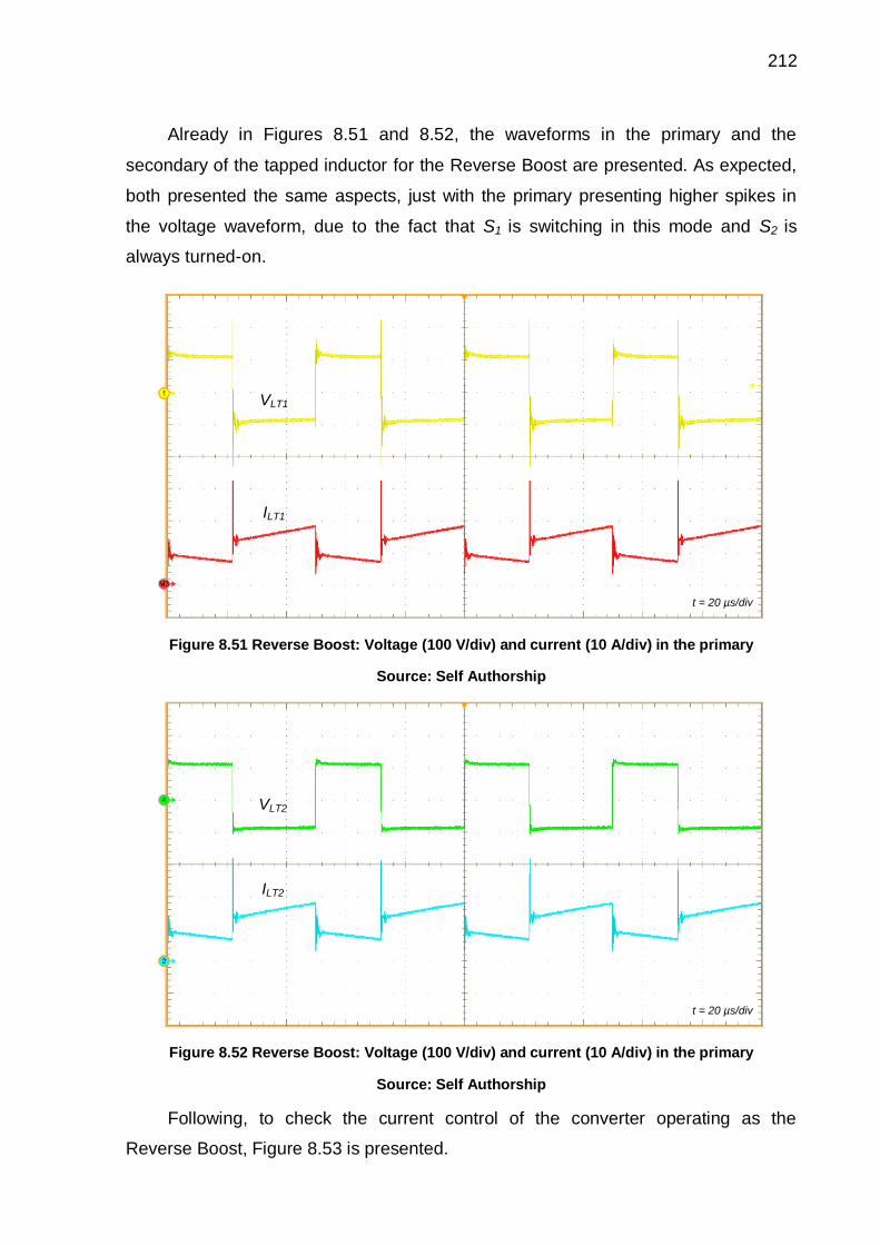
212
Already in Figures 8.51 and 8.52, the waveforms in the primary and the
secondary of the tapped inductor for the Reverse Boost are presented. As expected,
both presented the same aspects, just with the primary presenting higher spikes in
the voltage waveform, due to the fact that S1 is switching in this mode and S2 is
always turned-on.
ILT1
VLT1
t = 20 µs/div
Figure 8.51 Reverse Boost: Voltage (100 V/div) and current (10 A/div) in the primary
Source: Self Authorship
t = 20 µs/div
VLT2
ILT2
Figure 8.52 Reverse Boost: Voltage (100 V/div) and current (10 A/div) in the primary
Source: Self Authorship
Following, to check the current control of the converter operating as the
Reverse Boost, Figure 8.53 is presented.
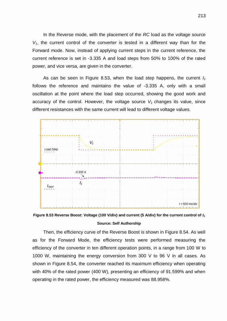
213
In the Reverse mode, with the placement of the RC load as the voltage source
V1, the current control of the converter is tested in a different way than for the
Forward mode. Now, instead of applying current steps in the current reference, the
current reference is set in -3.335 A and load steps from 50% to 100% of the rated
power, and vice versa, are given in the converter.
As can be seen in Figure 8.53, when the load step happens, the current I1
follows the reference and maintains the value of -3.335 A, only with a small
oscillation at the point where the load step occurred, showing the good work and
accuracy of the control. However, the voltage source V1 changes its value, since
different resistances with the same current will lead to different voltage values.
t = 500 ms/div
IREF
I1
V1
Load Step
-3.335 A
Figure 8.53 Reverse Boost: Voltage (100 V/div) and current (5 A/div) for the current control of I1
Source: Self Authorship
Then, the efficiency curve of the Reverse Boost is shown in Figure 8.54. As well
as for the Forward Mode, the efficiency tests were performed measuring the
efficiency of the converter in ten different operation points, in a range from 100 W to
1000 W, maintaining the energy conversion from 300 V to 96 V in all cases. As
shown in Figure 8.54, the converter reached its maximum efficiency when operating
with 40% of the rated power (400 W), presenting an efficiency of 91.599% and when
operating in the rated power, the efficiency measured was 88.958%.
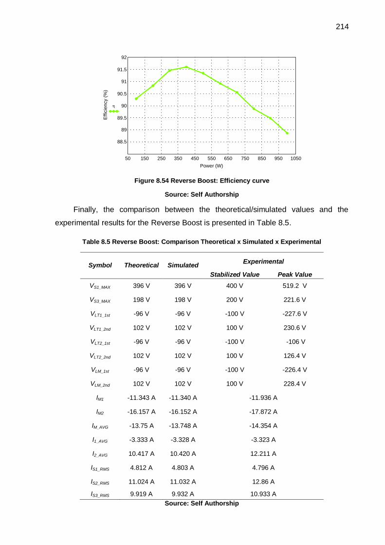
214
50 150 250 350 450 550 650 750 850 950 1050
88.5
89
89.5
90
90.5
91
91.5
92
Power (W)
Effic
ien
cy (
%)
Figure 8.54 Reverse Boost: Efficiency curve
Source: Self Authorship
Finally, the comparison between the theoretical/simulated values and the
experimental results for the Reverse Boost is presented in Table 8.5.
Table 8.5 Reverse Boost: Comparison Theoretical x Simulated x Experimental
Symbol Theoretical Simulated Experimental
Stabilized Value Peak Value
VS1_MAX 396 V 396 V 400 V 519.2 V
VS3_MAX 198 V 198 V 200 V 221.6 V
VLT1_1st -96 V -96 V -100 V -227.6 V
VLT1_2nd 102 V 102 V 100 V 230.6 V
VLT2_1st -96 V -96 V -100 V -106 V
VLT2_2nd 102 V 102 V 100 V 126.4 V
VLM_1st -96 V -96 V -100 V -226.4 V
VLM_2nd 102 V 102 V 100 V 228.4 V
IM1 -11.343 A -11.340 A -11.936 A
IM2 -16.157 A -16.152 A -17.872 A
IM_AVG -13.75 A -13.748 A -14.354 A
I1_AVG -3.333 A -3.328 A -3.323 A
I2_AVG 10.417 A 10.420 A 12.211 A
IS1_RMS 4.812 A 4.803 A 4.796 A
IS2_RMS 11.024 A 11.032 A 12.86 A
IS3_RMS 9.919 A 9.932 A 10.933 A
Source: Self Authorship

215
From the analysis of the experimental results of the Reverse Boost, it is
possible to see that the converter presented satisfactory results, where the
experimental results presented very close values when compared with the
theoretical/simulated values. As well as for the Forward Mode, the leakage
inductance and the reverse recovery phenomenon of the antiparallel-body diode of
the switches continued to show significant influence in the converter operation for the
Reverse mode.
About the converter efficiency, even presenting a lower efficiency if compared
with the Forward Buck, the converter showed a very good efficiency (between 88.9%
and 92 %), showing that the complementary operations Forward Buck/Reverse Boost
are a good option for an experimental implementation.
8.4.4 Reverse Buck-Boost
Following, the experimental results of the last operating mode are presented.
First, the gate signals for the Reverse Buck-Boost are shown in Figure 8.55.
t = 20 µs/div
VgS1
VgS3
VgS2
Figure 8.55 Reverse Buck-Boost: Gate signals (10 V/div)
Source: Self Authorship
In the same way as for the Forward Buck and the Reverse Boost, the Forward
Buck-Boost and the Reverse Buck-Boost present the same gate signals
configuration, where the operation of the converter is defined just setting a positive
(Forward mode) or a negative (Reverse mode) current reference.
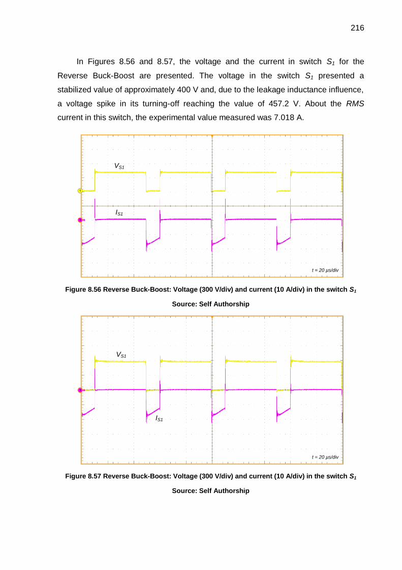
216
In Figures 8.56 and 8.57, the voltage and the current in switch S1 for the
Reverse Buck-Boost are presented. The voltage in the switch S1 presented a
stabilized value of approximately 400 V and, due to the leakage inductance influence,
a voltage spike in its turning-off reaching the value of 457.2 V. About the RMS
current in this switch, the experimental value measured was 7.018 A.
t = 20 µs/div
VS1
IS1
Figure 8.56 Reverse Buck-Boost: Voltage (300 V/div) and current (10 A/div) in the switch S1
Source: Self Authorship
t = 20 µs/div
VS1
IS1
Figure 8.57 Reverse Buck-Boost: Voltage (300 V/div) and current (10 A/div) in the switch S1
Source: Self Authorship

217
Then, using the zoom function of the oscilloscope in Figure 8.57, the turning-on
and the turning-off of the switch S1 are presented, respectively, by Figures 8.58 and
8.59.
t = 20 µs/div
VS1
IS1
Figure 8.58 Reverse Buck-Boost: Turning-on of the switch S1
Source: Self Authorship
t = 20 µs/div
VS1
IS1
Clamping Action
IGBT Tail Current
Figure 8.59 Reverse Buck-Boost: Turning-off of the switch S1
Source: Self Authorship
After the experimental waveforms of the switch S1 being presented, in Figures
8.60 and 8.61 the experimental results from switch S2 for the Reverse Buck-Boost
are presented where the maximum voltage reached in this switch was 592.8 V and
the RMS value of the current was 14.163 A. However, after the initial voltage spike, it
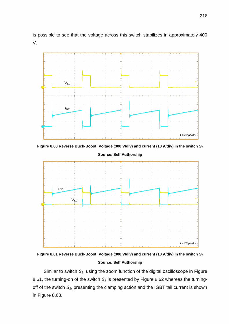
218
is possible to see that the voltage across this switch stabilizes in approximately 400
V.
t = 20 µs/div
VS2
IS2
Figure 8.60 Reverse Buck-Boost: Voltage (300 V/div) and current (10 A/div) in the switch S2
Source: Self Authorship
t = 20 µs/div
VS2
IS2
Figure 8.61 Reverse Buck-Boost: Voltage (300 V/div) and current (10 A/div) in the switch S2
Source: Self Authorship
Similar to switch S1, using the zoom function of the digital oscilloscope in Figure
8.61, the turning-on of the switch S2 is presented by Figure 8.62 whereas the turning-
off of the switch S2, presenting the clamping action and the IGBT tail current is shown
in Figure 8.63.

219
t = 20 µs/div
VS2 IS2
Figure 8.62 Reverse Buck-Boost: Turning-on of the switch S2
Source: Self Authorship
IGBT Tail Current
t = 20 µs/div
VS2
IS2
Clamping Action
Figure 8.63 Reverse Buck-Boost: Turning-off of the switch S2
Source: Self Authorship
In Figures 8.64 and 8.65, the voltage and current waveforms in the voltage
sources are presented.
In the voltage source V1, the average current was -3.363 A whereas in the
voltage source V2 this value was 12.712 A. About the voltage in each voltage source,
both presented the expected values, 300 V in V1 and 96 V in V2.
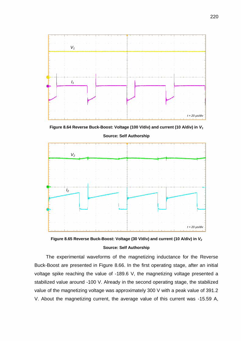
220
V1
I1
t = 20 µs/div
Figure 8.64 Reverse Buck-Boost: Voltage (100 V/div) and current (10 A/div) in V1
Source: Self Authorship
t = 20 µs/div
V2
I2
Figure 8.65 Reverse Buck-Boost: Voltage (30 V/div) and current (10 A/div) in V2
Source: Self Authorship
The experimental waveforms of the magnetizing inductance for the Reverse
Buck-Boost are presented in Figure 8.66. In the first operating stage, after an initial
voltage spike reaching the value of -189.6 V, the magnetizing voltage presented a
stabilized value around -100 V. Already in the second operating stage, the stabilized
value of the magnetizing voltage was approximately 300 V with a peak value of 391.2
V. About the magnetizing current, the average value of this current was -15.59 A,

221
and, disregarding the current spikes, the instantaneous values measured were -
12.793 A and -18.227 A.
t = 20 µs/div
VLM
IM
Figure 8.66 Reverse Buck-Boost: Voltage (200 V/div) and current (10 A/div) in the magnetizing inductance
Source: Self Authorship
In Figure 8.67 the currents through the switches are shown. The switches S1, S2
and S3 presented, respectively, the RMS values of 7.018 A, 14.163 A and 15.195 A.
t = 20 µs/div
IS3
IS1
IS2
Figure 8.67 Reverse Buck-Boost: Currents (20 A/div) through each switch
Source: Self Authorship
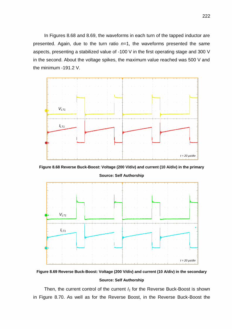
222
In Figures 8.68 and 8.69, the waveforms in each turn of the tapped inductor are
presented. Again, due to the turn ratio n=1, the waveforms presented the same
aspects, presenting a stabilized value of -100 V in the first operating stage and 300 V
in the second. About the voltage spikes, the maximum value reached was 500 V and
the minimum -191.2 V.
t = 20 µs/div
ILT1
VLT1
Figure 8.68 Reverse Buck-Boost: Voltage (200 V/div) and current (10 A/div) in the primary
Source: Self Authorship
t = 20 µs/div
VLT1
ILT1
Figure 8.69 Reverse Buck-Boost: Voltage (200 V/div) and current (10 A/div) in the secondary
Source: Self Authorship
Then, the current control of the current I1 for the Reverse Buck-Boost is shown
in Figure 8.70. As well as for the Reverse Boost, in the Reverse Buck-Boost the
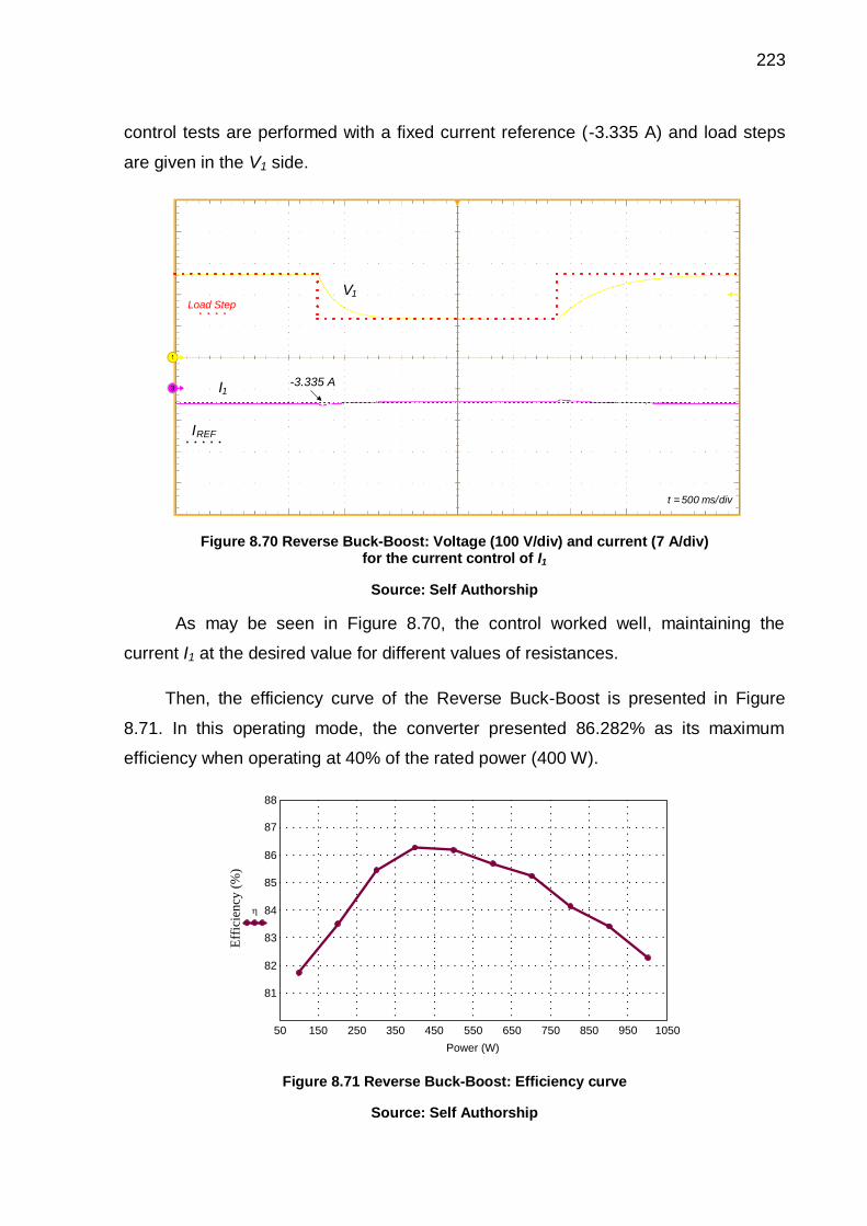
223
control tests are performed with a fixed current reference (-3.335 A) and load steps
are given in the V1 side.
-3.335 A
t = 500 ms/div
IREF
I1
Load Step
V1
Figure 8.70 Reverse Buck-Boost: Voltage (100 V/div) and current (7 A/div) for the current control of I1
Source: Self Authorship
As may be seen in Figure 8.70, the control worked well, maintaining the
current I1 at the desired value for different values of resistances.
Then, the efficiency curve of the Reverse Buck-Boost is presented in Figure
8.71. In this operating mode, the converter presented 86.282% as its maximum
efficiency when operating at 40% of the rated power (400 W).
50 150 250 350 450 550 650 750 850 950 1050
81
82
83
84
85
86
87
88
Power (W)
Eff
icie
ncy
(%
)
Figure 8.71 Reverse Buck-Boost: Efficiency curve
Source: Self Authorship
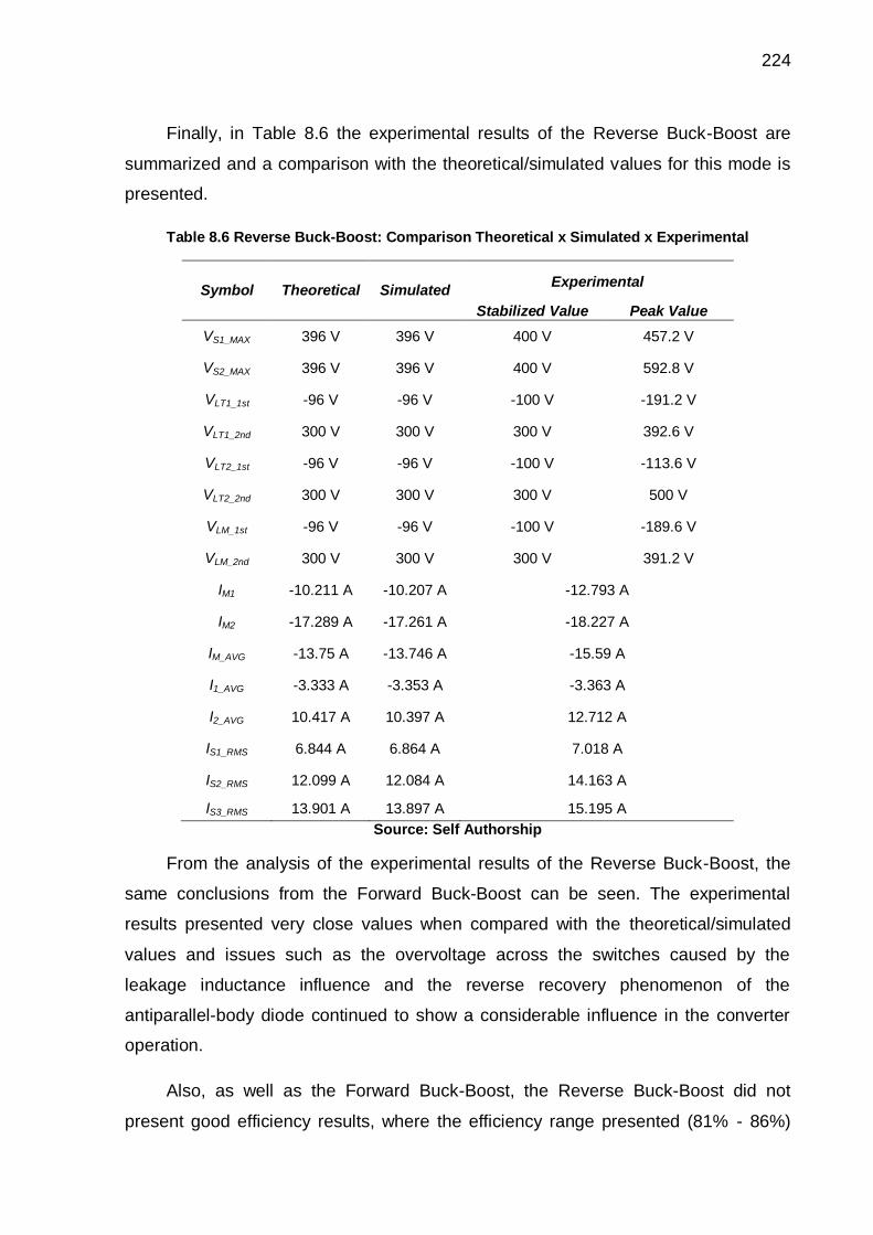
224
Finally, in Table 8.6 the experimental results of the Reverse Buck-Boost are
summarized and a comparison with the theoretical/simulated values for this mode is
presented.
Table 8.6 Reverse Buck-Boost: Comparison Theoretical x Simulated x Experimental
Symbol Theoretical Simulated Experimental
Stabilized Value Peak Value
VS1_MAX 396 V 396 V 400 V 457.2 V
VS2_MAX 396 V 396 V 400 V 592.8 V
VLT1_1st -96 V -96 V -100 V -191.2 V
VLT1_2nd 300 V 300 V 300 V 392.6 V
VLT2_1st -96 V -96 V -100 V -113.6 V
VLT2_2nd 300 V 300 V 300 V 500 V
VLM_1st -96 V -96 V -100 V -189.6 V
VLM_2nd 300 V 300 V 300 V 391.2 V
IM1 -10.211 A -10.207 A -12.793 A
IM2 -17.289 A -17.261 A -18.227 A
IM_AVG -13.75 A -13.746 A -15.59 A
I1_AVG -3.333 A -3.353 A -3.363 A
I2_AVG 10.417 A 10.397 A 12.712 A
IS1_RMS 6.844 A 6.864 A 7.018 A
IS2_RMS 12.099 A 12.084 A 14.163 A
IS3_RMS 13.901 A 13.897 A 15.195 A
Source: Self Authorship
From the analysis of the experimental results of the Reverse Buck-Boost, the
same conclusions from the Forward Buck-Boost can be seen. The experimental
results presented very close values when compared with the theoretical/simulated
values and issues such as the overvoltage across the switches caused by the
leakage inductance influence and the reverse recovery phenomenon of the
antiparallel-body diode continued to show a considerable influence in the converter
operation.
Also, as well as the Forward Buck-Boost, the Reverse Buck-Boost did not
present good efficiency results, where the efficiency range presented (81% - 86%)
225
makes unfeasible the use of this operation for the application addressed in this
thesis.
8.5 CHAPTER CONCLUSION
In this chapter, all the experimental results for the bidirectional DC-DC converter
with tapped inductor were presented and discussed. Analyzing the results presented
by the waveforms and the values presented from Tables 8.3 to 8.6, it is possible to
conclude that the experimental implementation was satisfactory, where the
experimental waveforms presented format with high similarity when compared with
the expected theoretical/simulated waveforms. Also, the experimental values were
very close do the theoretical/simulated values, where just the currents in the
converter presented some significant differences, which was an expected fact, since
the converter was analyzed and simulated with ideal elements, and in an
experimental implementation the losses in the converter components interfere
directly in those aspects.
About the operations, the Forward Buck/Reverse Boost presented good
efficiency results, supporting the use of this topology/operation in a commercial
application. On the other hand, the Forward Buck-Boost/Reverse Buck-Boost did not
present good efficiency results, and improvements such as the use of better
components or an optimization in the converter layout must be considered for this
mode. However, it was already expected that the Buck-Boost operation would
present less efficiency than the Forward Buck/Reverse Boost since the Buck-Boost
operations presented higher values in their RMS currents through the switches.
Other important aspects to be highlighted are the considerable influence of the
leakage inductance and the reverse recovery phenomenon of the antiparallel-body
diodes of the switches, aspects that are very difficult to deal in an experimental
implementation.
Nevertheless, for the leakage inductance effect the use of a RCD clamping
circuit showed to be a good solution whereas for the problem related to the reverse
recovery phenomenon of the antiparallel-body diode of the switches, a possible
solution is the use of better/faster power components.
226
CONCLUSION
In this Master’s Thesis, the study of two bidirectional topologies for HESS in
EVs applications was presented. In the first two chapters, after a careful bibliographic
review, the topics that hold the proposal of this work, such as EVs, HESS and
bidirectional DC-DC converters were discussed, giving the fundamental background
for the development of this research.
Then, in the chapters that followed, the first topology studied in this Master ’s
Thesis, the bidirectional DC-DC converter with tapped inductor, was analyzed in
details, leading to the construction of an experimental prototype for laboratory
implementation. The study of the converter included, among others, the theoretical
steady state and dynamic analyzes, the proposal of a design methodology
subsequently verified by a digital simulation performed in the power electronics
simulation software PSIM®, and, as mentioned earlier, the construction of an
experimental prototype.
About the experimental results of the first topology, the results were considered
satisfactory, since the values and the format of the waveforms were very close to the
expected theoretical values/waveforms. However, for 2 of the 4 implemented
operations, the Forward and the Reverse Buck-Boost, the efficiency results were not
good, demanding future improvements in the converter.
Already for the second topology, the bidirectional ZVS Buck-Boost DC-DC
converter, its study was restricted only to the theoretical steady state analysis and
the proposal of a design methodology subsequently verified by a digital simulation.
This can be explained due to the fact that, as this topology is a new proposal of this
present thesis, the authors are aiming for a feedback if this topology is worth of
further investigation, since in the authors vision, considering the problem related to
the efficiency results of the Buck-Boost operation in the first topology, this converter
could be a suitable alternative when Buck-Boost operations are needed.
Finally, as possible alternatives of future works derived from this thesis, the
following are suggested:

227
Study of different bidirectional DC-DC topologies and switching techniques
applied in HESS and EVs;
Improvement in the efficiency of the bidirectional DC-DC converter with
tapped inductor for the Forward and the Reverse Buck-Boost operation;
Implementation of the bidirectional DC-DC converter with tapped inductor
using a battery and a SC as voltage sources;
Dynamic analysis and control design for the bidirectional ZVS Buck-Boost
DC-DC converter;
Construction of the bidirectional ZVS Buck-Boost DC-DC converter;
Implementation of the bidirectional ZVS Buck-Boost DC-DC converter using
a battery and a SC as voltage sources.

228
REFERENCES
BARAN, R. The Introduction of Electric Vehicles in Brazil: Analyzing the Impact on Gasoline and Electricity Consumption. 2012. Doctoral Thesis (Degree of
Doctor of Science) – Federal University of Rio de Janeiro, Rio de Janeiro, 2012.
BARAN, R.; LEGEY, L. F. L. Electric Vehicles: History and Prospects in Brazil. BNDES Setorial, vol. 33, pp 207-224, 2010. Available at: < https://web.bndes.gov.br >. Access in March 2016.
BARBI, I.; MARTINS, D. C. Conversores CC-CC Básicos Não Isolados. 2 ed. Editora do Autor, 2000.
BELLUR, D. M.; KAZIMIERCZUK, M. K. DC-DC Converters for Electric Vehicle Applications. IEEE Electrical Insulation Conference and Electrical Manufacturing Expo 2007, October 2007.
BOCKLISCH, T. Hybrid Energy Storage Systems for Renewable Energy Applications. 9th International Renewable Energy Storage Conference (IRES) 2015, March 2015.
CASTRO, B. H. R.; FERREIRA, T. T. Electric Vehicles: Basic aspects, prospects and opportunities. BNDES Setorial, vol. 32, pp 267-310, 2010.
CARDOSO, R. L. Isolated Bidirectional DC-AC Converters in High Frequency. 2007. Doctoral Thesis (Doctoral Degree in Electrical Engineering) – Federal University of Santa Catarina, Florianópolis, 2007.
CARICCHI, F; CRESCIMBINI, F.; CAPPONI, F. G.; SOLERO, L. Study of a Bi-Directional Buck-Boost Converter Topologies for Application in Electric Vehicle Motor Drives. Applied Power Electronics Conference and Exposition, February 1998.
229
CAO, J.; EMADI, A. A New Battery/Ultracapacitor Hybrid Energy Storage System for Electric, Hybrid, and Plug-In Hybrid Electric Vehicles. IEEE Transactions on Power Electronics, vol. 27, no.1, pp. 122-132, January 2012.
CHAN, C.; CHAU, K. T. An Overview of Electric Vehicles – Challenges and Opportunities. IEEE 22nd International Conference on Industrial Electronics, Control and Instrumentation (IECON) 1996, August 1996.
CHAN, C.; CHAU, K. T. An Overview of Power Electronics in Electric Vehicles. IEEE Transactions on Industrial Electronics, vol. 44, no.1, pp. 3-13, February 1997.
CHAN, C.; CHAU, K. T. Power Electronics Challenges in Electric Vehicles. IEEE International Conference on Industrial Electronics, Control and Instrumentation (IECON) 1993, November 1993.
CHOI, M.; LEE, J.; SEO, S. Real-Time Optimization for Power Management Systems of a Battery/Supercapacitor Hybrid Energy Storage System in Electric Vehicles. IEEE Transactions on Vehicular Technology, vol. 63, no.8, pp. 3600-3611, February
2014.
CURTI, J. M. A.; HUANG, X.; MINAKI, R.; HORI, Y. A Simplified Power Management Strategy for a Supercapacitor/Battery Hybrid Energy Storage System Using the Half-Controlled Converter. 38th Annual Conference on IEEE Industrial Electronics Society (IECON) 2012, December 2012.
DE SOUZA, E. V. Symmetrical Isolated Bidirectional DC-DC Converters with Low Current Ripple. 2015. Doctoral Thesis (Doctoral Degree in Electrical Engineering) – Federal University of Santa Catarina, Florianópolis, 2015.
DOS SANTOS, C. A. Analysis and Design of a NPC Converter for Grid-Connected Energy Conversion Systems. 2011. Master’s Thesis (Master’s Degree in Electrical Engineering) – Federal University of Ceará, Fortaleza, 2011.

230
EMADI, A.; LEE, Y.; RAJASHEKARA, K. Power Electronics and Motor Drives in Electric, Hybrid Electric, and Plug-In Hybrid Electric Vehicles. IEEE Transactions on Industrial Electronics, vol. 55, no.6, pp. 2237-2245, June 2008.
EMADI, A.; WILLIAMSON, S.; KHALIGH, A. Power Electronics Intensive Solutions for Advanced Electric, Hybrid Electric, and Fuel Cell Vehicular Power Systems. IEEE Transactions on Power Electronics, vol. 21, no.3, pp. 567-577, May 2006.
ERICKSON, R. W.; MAKSIMOVIC, D. Fundamentals of Power Electronics. 2 ed.
New York: Kluwer Academic, 2001.
HINKLE, C.; MILLNER, A.; ROSS, W. Bidirectional Power Architectures for Electric Vehicles. 8th International Conference & Expo on Emerging Technologies for a Smarter World (CEWIT) 2011, November 2011.
HREDZAK, B.; AGELIDIS, V. G.; DEMETRIADES, G. D. A Low Complexity Control System for a Hybrid DC Power Source Based on Ultracapacitor-Lead-Acid Battery Configuration. IEEE Transactions on Power Electronics, vol. 29, no.6, pp. 2882-
2891, June 2014.
HUANG, X.; CURTI, J. M. A; HORI, Y. Energy Management Strategy with Optimized Power Interface for the Battery Supercapacitor Hybrid System of Electric Vehicles. 39th Annual Conference on IEEE Industrial Electronics Society (IECON) 2013, December 2013.
HYUN-LARK DO. Nonisolated Bidirectional Zero-Voltage-Switching DC-DC Converter. IEEE Transactions on Power Electronics, vol. 26, no.9, pp. 2563-2569, September 2011.
KHAN, A. A.; CHA, H.; AHMED, H. F. A Family of High Efficiency Bidirectional DC-DC Converters Using Switching Cell Structure. IEEE 8th International Power Electronics and Motion Control Conference (IPEMC-ECCE ASIA) 2016, May 2016.
231
KOLLIMALLA, S. K; MISHRA, M. K; NARASAMMA; N. L. Design and Analysis of Novel Control Strategy for Battery and Supercapacitor Storage System. IEEE Transactions on Sustainable Energy, vol. 5, no.4, pp. 1137-1144, October 2014.
LAFUENTE, C. Single-Phase Battery Charger Feasible for Electric Vehicles Applications. 2011. Master’s Thesis (Master’s Degree in Electrical Engineering) – Federal University of Ceará, Fortaleza, 2011.
LIU, W.; CHEN, J.; LIANG, T.; LIN, R.; LIU, C. Analysis, Design, and Control of Bidirectional Cascaded Configuration for a Fuel Cell Hybrid Power System. IEEE Transactions on Power Electronics, vol. 25, no.6, pp. 1565-1575, June 2010.
MAYER, R.; PÉRES, A.; GARCIA OLIVEIRA, S. V. Multiphase Bidirectional DC/DC Non-Isolated Converter for Electric Drive System in Electric Vehicle and Hybrid Electric Vehicle. Power Electronics Magazine, Campo Grande, vol. 20, no. 3, pp. 311-321, June-August 2015.
MIRZAEI, M.; AFZALIAN, A. A. Explicit Model Predictive Control of the Non-Inverting Buck Boost DC-DC Converter. International Conference on Control, Automation and Systems 2008, October 2008.
NA, W.; GOU, B. Analysis and Control of Bidirectional DC/DC Converter for PEM fuel cell applications. IEEE Power and Energy Society General Meeting – Conversion and Delivery of Electrical Energy in the 21st Century 2008, July 2008.
OGATA, K. Modern Control Engineering. 4 ed. Prentice Hall Brasil, 2003.
OIH YU, A. S.; CORREIA SILVA, L. L.; CHU, C. L.; NASCIMENTO, P. T.; CAMARGO, A. S. Electric Vehicles: Struggles in creating a market. Proceedings of PICMET’ 11: Technology Management in the Energy Smart World 2011, July
2011.

232
OUCHI, T.; KANOUDA, A.; TAKAHASHI, N. Parallel Bi-Directional DC-DC Converter
for Energy Storage System. International Power Electronics Conference (IPEC-
Hiroshima 2014 – ECCE-ASIA) 2014, May 2014.
OUCHI, T.; KANOUDA, A.; TAKAHASHI, N.; MOTEKI, M. Seamless Controlled Parallel Bi-Directional DC-DC Converter for Energy Storage System. 16th European Conference on Power Electronics and Applications 2014 (EPE’ 14- ECCE Europe), August 2014.
PERAÇA, M. T. DC-DC Boost Converter Applied to Refrigeration Systems. 2002.
Master’s Thesis (Master’s Degree in Electrical Engineering) – Federal University of Santa Catarina, Florianópolis, 2002.
RESTREPO, C.; CALVENTE, J.; CID-PASTOR, A.; EL AROUDI, A.; GIRAL, R. A Noninverting Buck-Boost DC-DC Switching Converter with High Efficiency and Wide Bandwidth. IEEE Transactions on Power Electronics, vol. 26, no.9, pp. 2536-2549,
September 2011.
RESTREPO, C.; CALVENTE, J.; ROMERO, A.; VIDAL-IDIARTE, E.; GIRAL, R. Current-Mode Control of a Coupled-Inductor Buck-Boost DC-DC Switching Converter. IEEE Transactions on Power Electronics, vol. 27, no.5, pp. 3648-3652, May 2012.
ROSEMBACK, R. H. Operation of a Buck-Boost Converter as Battery Charge Controller Connected to a Photovoltaic Generation System. 2004. Master’s Thesis (Master’s Degree in Electrical Engineering) – Federal University of Juiz de Fora, Juiz de Fora, 2004.
SPERANDIO, M.; SALDANHA, J. J.; BASSO, C. Impact of the Plug-In Hybrid Electric Vehicles in the Transmission System. Brazilian Congress of Automatics,
September 2012.
SULZBERGER, C. An early road warrior: electric vehicles in the early years of the automobile. IEEE Power and Energy Magazine, vol. 2, no.3, pp. 66-71, May-June 2004.

233
YUNMAO YE; CHENG, K. W. E, DING, K.; WANG, D.; BAO, Y. Hybrid Energy Storage System and Associated Converters Examination for DC Distribution. 5th International Conference on Power Electronics Systems and Applications (PESA) 2013, December 2013.

234
APPENDIX A – BIDIRECTIONAL DC-DC CONVERTER WITH TAPPED
INDUCTOR: BUCK/BOOST CALCULATIONS

235
Bidirectional DC-DC Converter with Tapped Inductor:
Buck/Boost Calculations
Voltage Source V1
Voltage Source V2
Turn ratio
Switching frequency
Rated power
Magnetizing Inductance
Duty Cycle - Switch S1
Duty Cycle - Switch S3
Resistive Load
Forward Buck
Resistive Load
Reverse Boost
For the Forward Buck/Reverse Boost, the switch S2 is always turned-on.
Forward Buck
V1 300 V( )
V2 96 V( )
n 1
fs 20000 Hz( )
PC 1000 W( )
Lm 513.711 106
H( )
D1 V21 n
V1 V2 n
D1 0.4848
D3 1 D1
D3 0.5152
RForward
V22
PC
RForward 9.216 ( )
RReverse
V12
PC
RReverse 90 ( )
VS1_max_Forward V1 n V2
VS1_max_Forward 396 V( )
VS3_max_Forward
V1 V2 1 n
V2

236
Voltage in the primary
(1st opt stg)
Voltage in the primary
(2nd opt stg)
Voltage in the secondary
(1st opt stg)
Voltage in the secondary
(2nd opt stg)
Magnetizing Current
Inst. value 2
Magnetizing Current
Inst. value 1
Magnetizing Current
Average
S1 - RMS current
VS3_max_Forward 198 V( )
VLT1_1st_Forward
n V1 V2
1 n
VLT1_1st_Forward 102 V( )
VLT1_2nd_Forward n V2
VLT1_2nd_Forward 96 V( )
VLT2_1st_Forward
V1 V2 1 n
VLT2_1st_Forward 102 V( )
VLT2_2nd_Forward V2
VLT2_2nd_Forward 96 V( )
IM2_F
2 PC n 1( )2
fs Lm V1 V1 V2 D12
n2
2 V1 D1 n n 1( ) fs Lm
IM2_F 16.157 A( )
IM1_F
2 PC n 1( )2
fs Lm V1 V1 V2 D12
n2
2 V1 D1 n n 1( ) fs Lm
IM1_F 11.343 A( )
IM_F
IM2_F IM1_F
2
IM_F 13.75 A( )
IS1_RMS_F1
2 V1 Lm fs n 1( )2
D14
V12
n4
V1 V2 2 12 Lm2
PC2
fs2
n 1( )4
3 D1
IS1_RMS_F 4.812 A( )
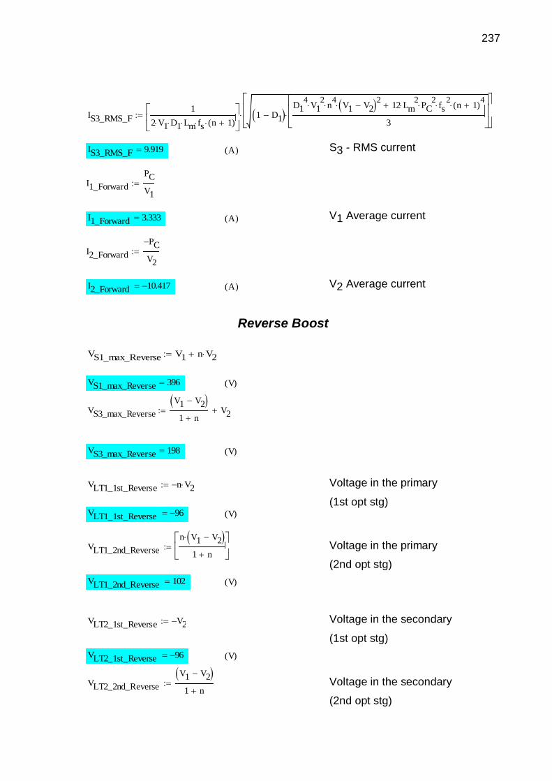
237
S3 - RMS current
V1 Average current
V2 Average current
Reverse Boost
Voltage in the primary
(1st opt stg)
Voltage in the primary
(2nd opt stg)
Voltage in the secondary
(1st opt stg)
Voltage in the secondary
(2nd opt stg)
IS3_RMS_F1
2 V1 D1 Lm fs n 1( )
1 D1 D1
4V1
2 n
4 V1 V2
2 12 Lm
2 PC
2 fs
2 n 1( )
4
3
IS3_RMS_F 9.919 A( )
I1_Forward
PC
V1
I1_Forward 3.333 A( )
I2_Forward
PC
V2
I2_Forward 10.417 A( )
VS1_max_Reverse V1 n V2
VS1_max_Reverse 396 V( )
VS3_max_Reverse
V1 V2 1 n
V2
VS3_max_Reverse 198 V( )
VLT1_1st_Reverse n V2
VLT1_1st_Reverse 96 V( )
VLT1_2nd_Reverse
n V1 V2
1 n
VLT1_2nd_Reverse 102 V( )
VLT2_1st_Reverse V2
VLT2_1st_Reverse 96 V( )
VLT2_2nd_Reverse
V1 V2 1 n

238
Magnetizing Current
Inst. value 2
Magnetizing Current
Inst. value 1
Magnetizing Current
Average
S1 - RMS current
S2 - RMS current
S3 - RMS current
V1 Average current
V2 Average current
VLT2_2nd_Reverse 102 V( )
IM2_R
2 PC n 1( ) fs Lm V1 V2 D3 1 D3 n2
2 V1 n 1 D3 fs Lm
IM2_R 16.157 A( )
IM1_R
2 PC n 1( ) fs Lm V1 V2 D3 1 D3 n2
2 V1 n 1 D3 fs Lm
IM1_R 11.343 A( )
IM_R
IM2_F IM1_F
2
IM_R 13.75 A( )
IS1_RMS_R1
6 V1 Lm fs n 1( )
3 D32
V12
V22
n4
D3 1 2
12 Lm2
PC2
fs2
n 1( )2
1 D3
IS1_RMS_R 4.812 A( )
IS2_RMS_R1
6 V1 Lm fs n 1( )
3 D32
V12
V22
n4
D3 1 2 1 D3 n2
2 D3 n
12 Lm
2 PC
2 fs
2 n 1( )
2D3 n n
34 n
2 5 n 2
D3 1 2
IS2_RMS_R 11.025 A( )
IS3_RMS_R1
6 V1 Lm fs
3D3
1 D3 2
D32
V22
V12
n4
D3 1 2
12 Lm2
PC2
fs2
n 1( )2
IS3_RMS_R 9.919 A( )
I1_Reverse
PC
V1
I1_Reverse 3.333 A( )
I2_Reverse
PC
V2
I2_Reverse 10.417 A( )

239
APPENDIX B - BIDIRECTIONAL DC-DC CONVERTER WITH TAPPED
INDUCTOR: BUCK-BOOST CALCULATIONS
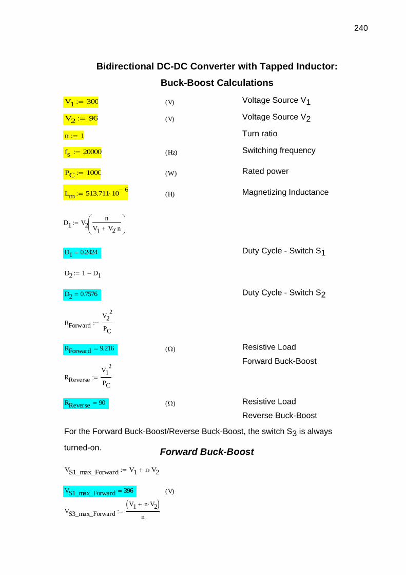
240
Bidirectional DC-DC Converter with Tapped Inductor:
Buck-Boost Calculations
Voltage Source V1
Voltage Source V2
Turn ratio
Switching frequency
Rated power
Magnetizing Inductance
Duty Cycle - Switch S1
Duty Cycle - Switch S2
Resistive Load
Forward Buck-Boost
Resistive Load
Reverse Buck-Boost
For the Forward Buck-Boost/Reverse Buck-Boost, the switch S3 is always
turned-on. Forward Buck-Boost
V1 300 V( )
V2 96 V( )
n 1
fs 20000 Hz( )
PC 1000 W( )
Lm 513.711 106
H( )
D1 V2n
V1 V2 n
D1 0.2424
D2 1 D1
D2 0.7576
RForward
V22
PC
RForward 9.216 ( )
RReverse
V12
PC
RReverse 90 ( )
VS1_max_Forward V1 n V2
VS1_max_Forward 396 V( )
VS3_max_Forward
V1 n V2 n

241
Voltage in the primary
(1st opt stg)
Voltage in the primary
(2nd opt stg)
Voltage in the secondary
(1st opt stg)
Voltage in the secondary
(2nd opt stg)
Magnetizing Current
Inst. value 2
Magnetizing Current
Inst. value 1
Magnetizing Current
Average
S1 - RMS current
VS3_max_Forward 396 V( )
VLT1_1st_Forward V1
VLT1_1st_Forward 300 V( )
VLT1_2nd_Forward n V2
VLT1_2nd_Forward 96 V( )
VLT2_1st_Forward
V1 n
VLT2_1st_Forward 300 V( )
VLT2_2nd_Forward V2
VLT2_2nd_Forward 96 V( )
IM2_F
2 PC fs Lm V12
D12
2 V1 D1 fs Lm
IM2_F 17.289 A( )
IM1_F
2 PC fs Lm V12
D12
2 V1 D1 fs Lm
IM1_F 10.211 A( )
IM_F
IM2_F IM1_F
2
IM_F 13.75 A( )
IS1_RMS_F1
6 V1 Lm fs
3D14
V14
36 Lm2
PC2
fs2
D1
IS1_RMS_F 6.844 A( )
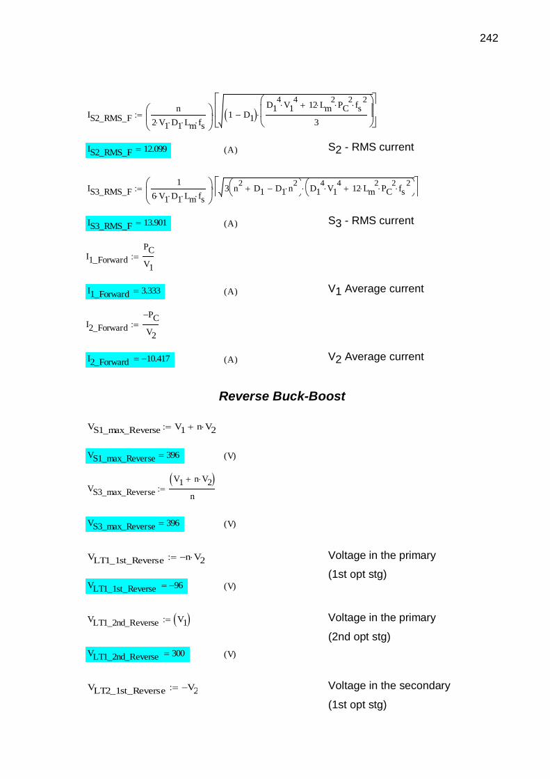
242
S2 - RMS current
S3 - RMS current
V1 Average current
V2 Average current
Reverse Buck-Boost
Voltage in the primary
(1st opt stg)
Voltage in the primary
(2nd opt stg)
Voltage in the secondary
(1st opt stg)
IS2_RMS_Fn
2 V1 D1 Lm fs
1 D1 D1
4V1
4 12 Lm
2 PC
2 fs
2
3
IS2_RMS_F 12.099 A( )
IS3_RMS_F1
6 V1 D1 Lm fs
3 n2
D1 D1 n2
D1
4V1
4 12 Lm
2 PC
2 fs
2
IS3_RMS_F 13.901 A( )
I1_Forward
PC
V1
I1_Forward 3.333 A( )
I2_Forward
PC
V2
I2_Forward 10.417 A( )
VS1_max_Reverse V1 n V2
VS1_max_Reverse 396 V( )
VS3_max_Reverse
V1 n V2 n
VS3_max_Reverse 396 V( )
VLT1_1st_Reverse n V2
VLT1_1st_Reverse 96 V( )
VLT1_2nd_Reverse V1
VLT1_2nd_Reverse 300 V( )
VLT2_1st_Reverse V2
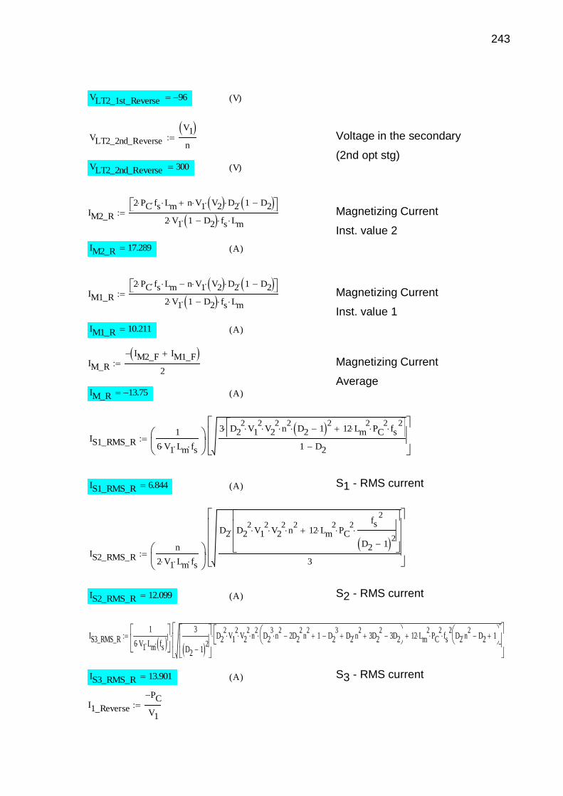
243
Voltage in the secondary
(2nd opt stg)
Magnetizing Current
Inst. value 2
Magnetizing Current
Inst. value 1
Magnetizing Current
Average
S1 - RMS current
S2 - RMS current
S3 - RMS current
VLT2_1st_Reverse 96 V( )
VLT2_2nd_Reverse
V1 n
VLT2_2nd_Reverse 300 V( )
IM2_R
2 PC fs Lm n V1 V2 D2 1 D2 2 V1 1 D2 fs Lm
IM2_R 17.289 A( )
IM1_R
2 PC fs Lm n V1 V2 D2 1 D2 2 V1 1 D2 fs Lm
IM1_R 10.211 A( )
IM_R
IM2_F IM1_F
2
IM_R 13.75 A( )
IS1_RMS_R1
6 V1 Lm fs
3 D22
V12
V22
n2
D2 1 2
12 Lm2
PC2
fs2
1 D2
IS1_RMS_R 6.844 A( )
IS2_RMS_Rn
2 V1 Lm fs
D2 D22
V12
V22
n2
12 Lm2
PC2
fs
2
D2 1 2
3
IS2_RMS_R 12.099 A( )
IS3_RMS_R1
6 V1 Lm fs
3
D2 1 2
D22
V12
V22
n2
D23
n2
2D22
n2
1 D23
D2 n2
3D22
3D2
12 Lm
2 PC
2 fs
2 D2 n
2 D2 1
IS3_RMS_R 13.901 A( )
I1_Reverse
PC
V1

244
V1 Average current
V2 Average current
I1_Reverse 3.333 A( )
I2_Reverse
PC
V2
I2_Reverse 10.417 A( )

245
APPENDIX C – BIDIRECTIONAL ZVS BUCK-BOOST DC-DC
CONVERTER: CALCULATIONS
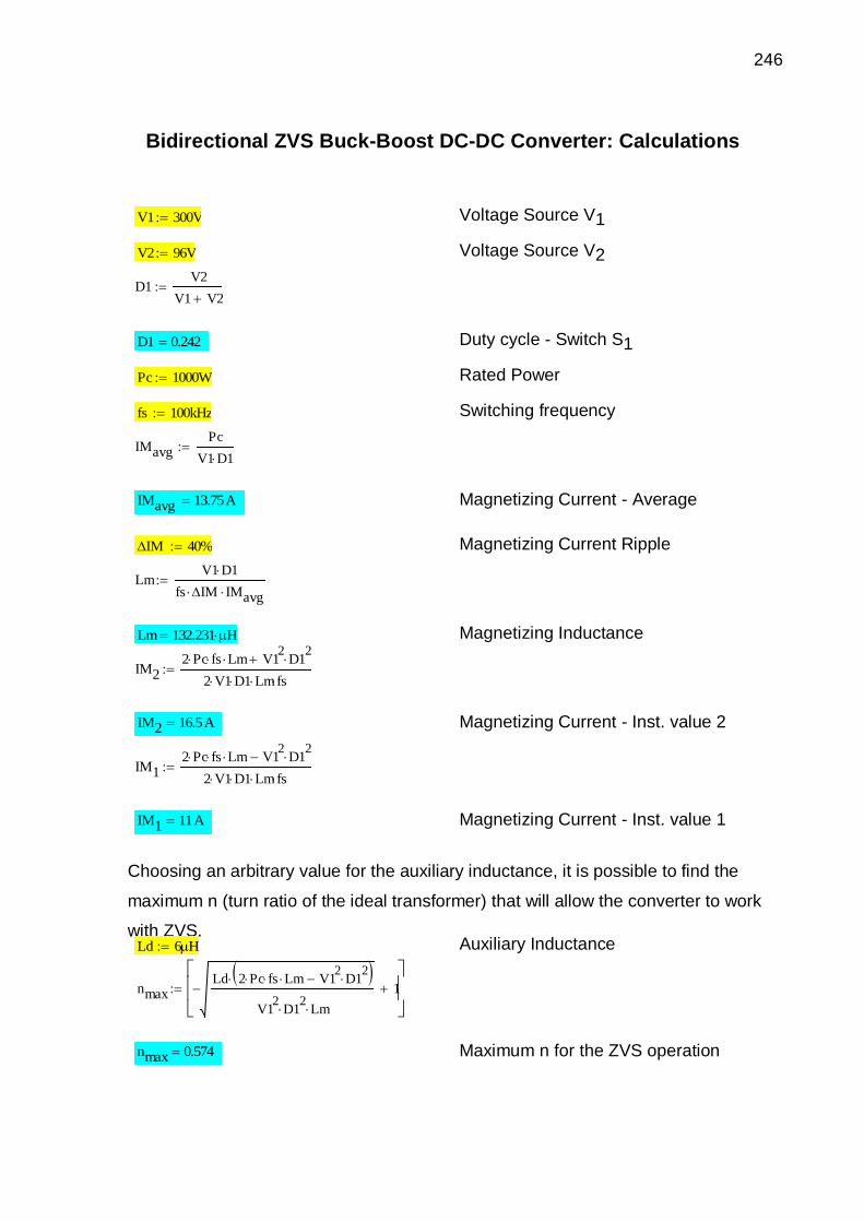
246
Bidirectional ZVS Buck-Boost DC-DC Converter: Calculations
Voltage Source V1
Voltage Source V2
Duty cycle - Switch S1
Rated Power
Switching frequency
Magnetizing Current - Average
Magnetizing Current Ripple
Magnetizing Inductance
Magnetizing Current - Inst. value 2
Magnetizing Current - Inst. value 1
Choosing an arbitrary value for the auxiliary inductance, it is possible to find the
maximum n (turn ratio of the ideal transformer) that will allow the converter to work
with ZVS. Auxiliary Inductance
Maximum n for the ZVS operation
V1 300V
V2 96V
D1V2
V1 V2
D1 0.242
Pc 1000W
fs 100kHz
IMavgPc
V1 D1
IMavg 13.75A
IM 40%
LmV1 D1
fs IM IMavg
Lm 132.231 H
IM22 Pc fs Lm V1
2D1
2
2 V1 D1 Lm fs
IM2 16.5A
IM12 Pc fs Lm V1
2D1
2
2 V1 D1 Lm fs
IM1 11A
Ld 6H
nmaxLd 2 Pc fs Lm V1
2D1
2
V12
D12
Lm
1
nmax 0.574
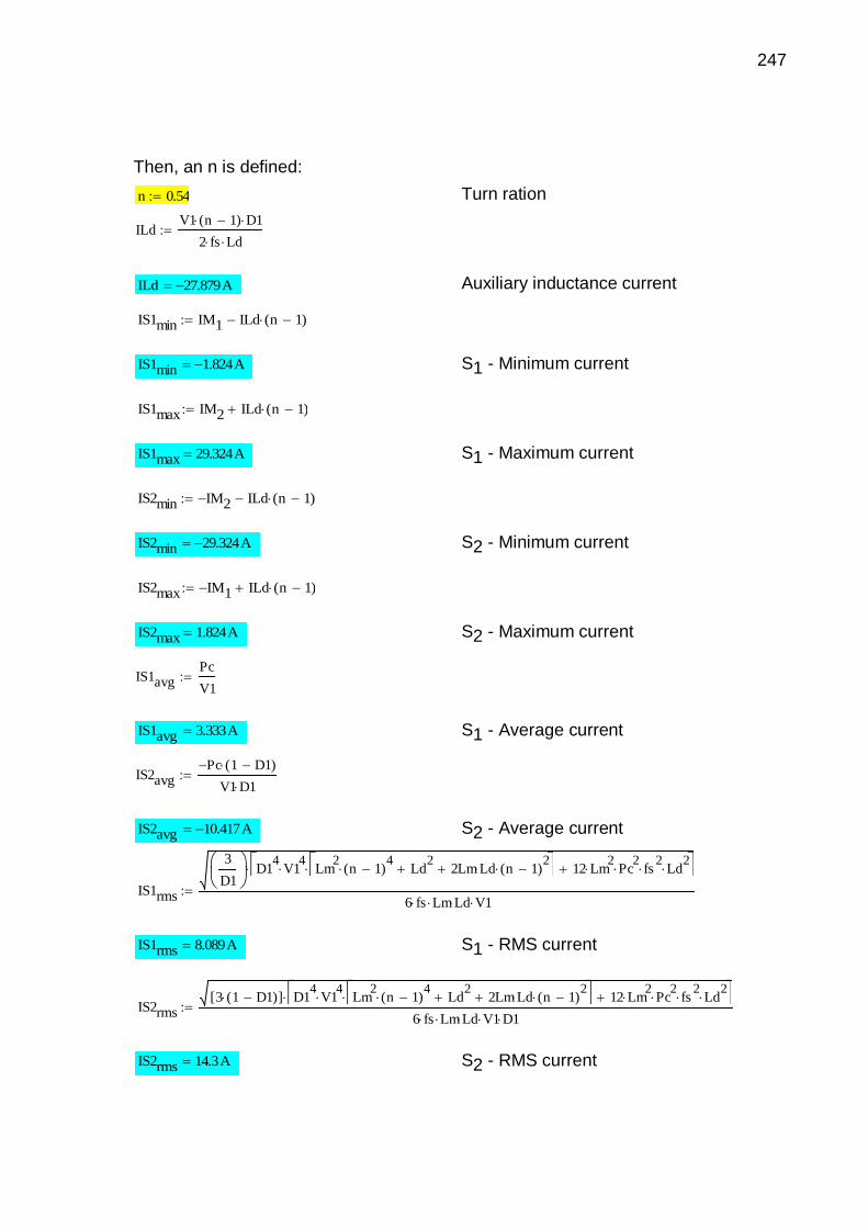
247
Then, an n is defined:
Turn ration
Auxiliary inductance current
S1 - Minimum current
S1 - Maximum current
S2 - Minimum current
S2 - Maximum current
S1 - Average current
S2 - Average current
S1 - RMS current
S2 - RMS current
n 0.54
ILdV1 n 1( ) D1
2 fs Ld
ILd 27.879 A
IS1min IM1 ILd n 1( )
IS1min 1.824 A
IS1max IM2 ILd n 1( )
IS1max 29.324A
IS2min IM2 ILd n 1( )
IS2min 29.324 A
IS2max IM1 ILd n 1( )
IS2max 1.824A
IS1avgPc
V1
IS1avg 3.333A
IS2avgPc 1 D1( )
V1 D1
IS2avg 10.417 A
IS1rms
3
D1
D14
V14
Lm2
n 1( )4
Ld2
2Lm Ld n 1( )2
12 Lm2
Pc2
fs2
Ld2
6 fs Lm Ld V1
IS1rms 8.089A
IS2rms3 1 D1( )[ ] D1
4V1
4 Lm
2n 1( )
4 Ld
2 2Lm Ld n 1( )
2 12 Lm
2 Pc
2 fs
2 Ld
2
6 fs Lm Ld V1 D1
IS2rms 14.3A
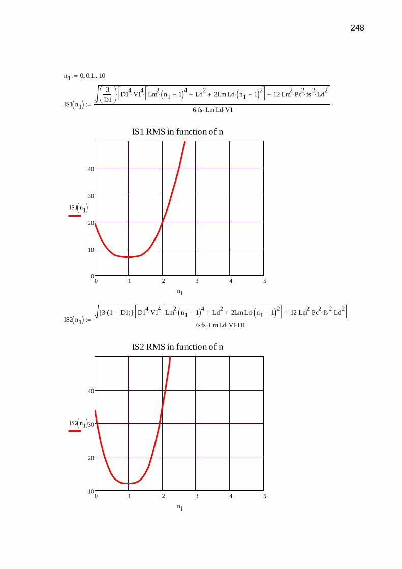
248
n1 0 0.1 10
IS1 n1
3
D1
D14
V14
Lm2
n1 1 4
Ld2
2Lm Ld n1 1 2
12 Lm
2 Pc
2 fs
2 Ld
2
6 fs Lm Ld V1
0 1 2 3 4 50
10
20
30
40
IS1 RMS in function of n
IS1 n1
n1
IS2 n1 3 1 D1( )[ ] D1
4V1
4 Lm
2n1 1
4 Ld
2 2Lm Ld n1 1
2
12 Lm
2 Pc
2 fs
2 Ld
2
6 fs Lm Ld V1 D1
0 1 2 3 4 510
20
30
40
IS2 RMS in function of n
IS2 n1
n1
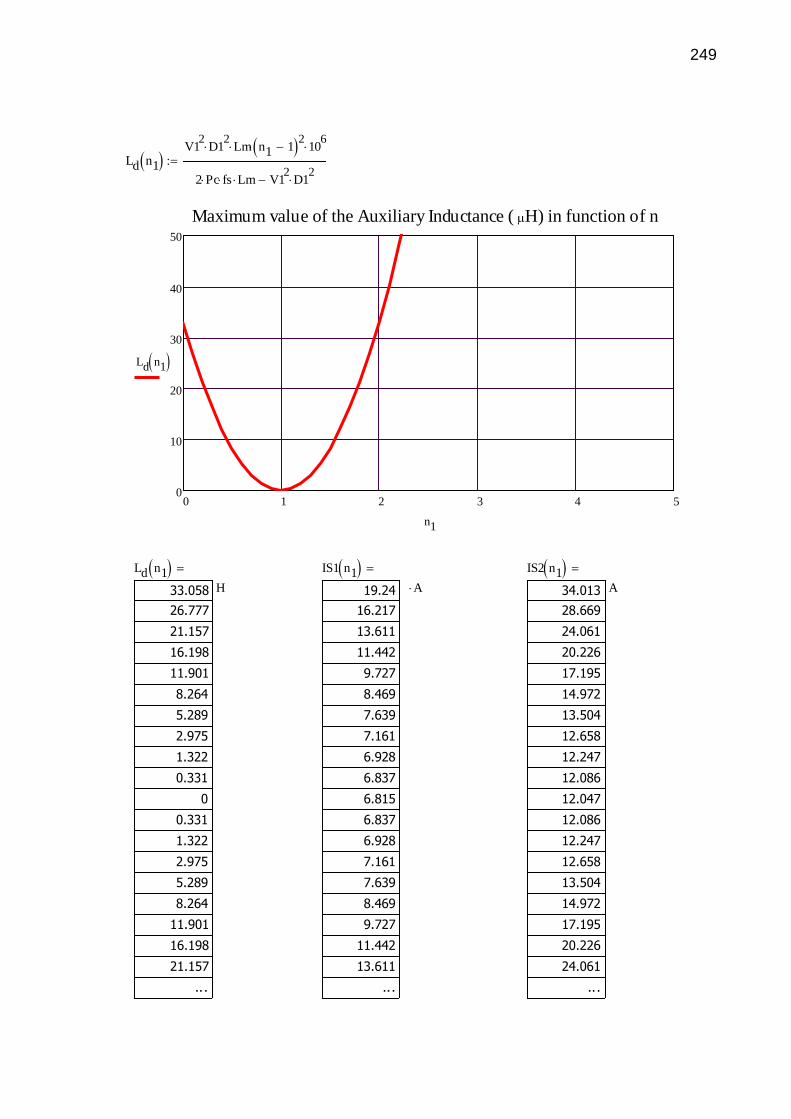
249
Ld n1 V1
2D1
2 Lm n1 1
2 10
6
2 Pc fs Lm V12
D12
0 1 2 3 4 50
10
20
30
40
50
Maximum value of the Auxiliary Inductance ( H) in function of n
Ld n1
n1
Ld n1 33.058
26.777
21.157
16.198
11.901
8.264
5.289
2.975
1.322
0.331
0
0.331
1.322
2.975
5.289
8.264
11.901
16.198
21.157
...
H
IS1 n1 19.24
16.217
13.611
11.442
9.727
8.469
7.639
7.161
6.928
6.837
6.815
6.837
6.928
7.161
7.639
8.469
9.727
11.442
13.611
...
A
IS2 n1 34.013
28.669
24.061
20.226
17.195
14.972
13.504
12.658
12.247
12.086
12.047
12.086
12.247
12.658
13.504
14.972
17.195
20.226
24.061
...
A

250
APPENDIX D – TAPPED INDUCTOR DESIGN
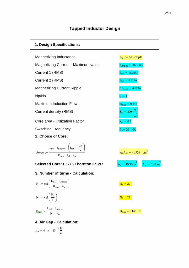
251
Tapped Inductor Design
1. Design Specifications:
Magnetizing Inductance
Magnetizing Current - Maximum value
Current 1 (RMS)
Current 2 (RMS)
Magnetizing Current Ripple
Np/Ns
Maximum Induction Flow
Current density (RMS)
Core area - Utilization Factor
Switching Frequency
2. Choice of Core:
Selected Core: EE-76 Thornton IP12R
3. Number of turns - Calculation:
4. Air Gap - Calculation:
Lm1 513.711H
ILmpico 16.158A
I1ef 11.025A
I2ef 4.811A
I Lm1 4.813A
a 1
Bmax 0.15T
Jef 300A
cm2
kw 0.7
f 20 kHz
AeAw
Lm1 ILmpico I1ef
I2ef
a
Bmax Jef kw AeAw 41.729 cm
4
Ae 19.35cm2
Aw 6.45cm2
N1 ceilLm1 ILmpico
Bmax Ae
N1 29
N2 ceilN1
a
N2 29
Bmax
Lm1 ILmpico
N1 Ae Bmax 0.148 T
o 4 107
H
m

252
5. Conductor gauge - Calculation:
Wire Diameter:
The selected wire is the 25AWG.
6. Losses - Calculation:
6.1 Wire Losses:
lent referro
N12
o Ae 102 m
cm
Lm1
lent referro 3.981 mm
7.5 s
0.5 cm
f 0.053 cm
Dfio 2 Dfio 0.106 cm
Sfio 0.001624 cm2
Sfioiso 0.002078 cm2
Scobre1
I1ef
Jef
Scobre1 0.037 cm2
ncond1 ceilScobre1
Sfio
ncond1 23
Scobre2
I2ef
Jef
Scobre2 0.016 cm2
ncond2 ceilScobre2
Sfio
ncond2 10
fio 0.001419
cm
lespira 21.8cm
lfio1 N1 lespira lfio1 6.322m
Rcobre1
fio lespira N1
ncond1
Rcobre1 39.004 103
lfio2 N2 lespira lfio2 6.322m
Rcobre2
fio lespira N2
ncond2
Rcobre2 89.709 103

253
6.2 Magnetic Losses:
6.3 Total Losses:
6.4 Core - Thermal Resistance:
Pcobre Rcobre1 I1ef2
Rcobre2 I2ef2
Pcobre 6.817 W
Vnucleo 421.35cm3
k 1.052W
m3
1.5 2.44
BLm1 I Lm1
N1 Ae
1
T B 0.044
Pnucleo kf
Hz
1
2B
Vnucleo Pnucleo 0.114 W
ki
k
2 ( ) 1
2
0
2
cos ( )
d
ki 0.063W
m3
Pv
f
Hz
ki B( )
0
Hz
2f
tB2f
Hz
d
0
Hz
2f
tB2f
Hz
d
Pv 0.246kW
m3
Pnucleo Pv Vnucleo Pnucleo 0.104 W
Ptotais Pcobre Pnucleo Pto tais 6.921 W
Rtnucleo 23K
W
Ae Aw
cm4
0.37
Rtnucleo 3.856K
W

254
6.5 Temperature Increasing:
7. Possibility of Execution:
T Pcobre Pnucleo Rtnucleo T 26.686K
Aw_min
N1 Sfioiso ncond1 N2 Sfioiso ncond2
kw
Aw_min 2.841 cm
2
ExecAw_min
Aw
Exec 0.44

255
APPENDIX E – VOLTAGE GAIN CIRCUIT
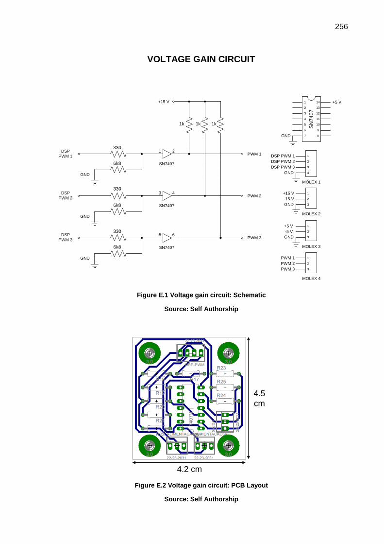
256
VOLTAGE GAIN CIRCUIT
1k 1k 1k
330
330
330
6k8
6k8
6k8
GND
GND
GND
DSP
PWM 1
DSP
PWM 2
DSP
PWM 3
1 2
3 4
5 6
SN7407
SN7407
SN7407
+15 V
PWM 1
PWM 2
PWM 3
1
2
3
4
5
6
7
14
13
12
11
10
9
8
+5 V
GND
SN
74
07
1
2
3
4
MOLEX 1
1
2
3
MOLEX 2
1
2
3
MOLEX 3
1
2
3
MOLEX 4
GND
GND
GND
DSP PWM 1
DSP PWM 2
DSP PWM 3
+15 V
-15 V
+5 V
-5 V
PWM 1
PWM 2
PWM 3
Figure E.1 Voltage gain circuit: Schematic
Source: Self Authorship
4.2 cm
4.5
cm
Figure E.2 Voltage gain circuit: PCB Layout
Source: Self Authorship
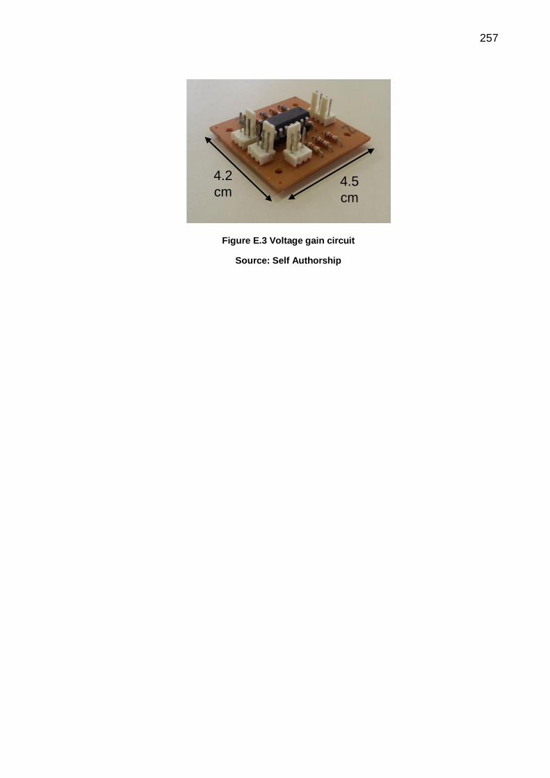
257
4.2
cm4.5
cm
Figure E.3 Voltage gain circuit
Source: Self Authorship

258
APPENDIX F – SIGNAL TREATMENT CIRCUIT
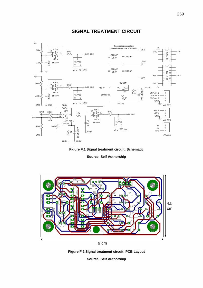
259
SIGNAL TREATMENT CIRCUIT
1
2
3
4
5
6
7
14
13
12
11
10
9
8
-15 V
GND
LF
34
7N
1
2
3
4
MOLEX 1
1
2
3
MOLEX 2
1
2
3
MOLEX 3
GND
GND
DSP AN 1
DSP AN 2
DSP AN 3
+15 V
-15 V
V1
V2
IMEAS
+15 V
1
2
3
4
8
7
6
5TL
77
26 +3 VGND4
11
41
1
41
1
41
1
1
7
814
2
3
6
5
9
10
13
12
+15 V
-15 V
+15 V
-15 V
+15 V
-15 V
+15 V
-15 V+15 V
560
560
560
56k
15k
560k
4.7k
100k
100k
100
100k
100k
5k
10
µF
/25
V
10k
GND
GND GND
GND
GND
GND GND
V1
V2
IMEAS
LF347N
LF347N
LF347NLF347N
DSP AN 1
DSP AN 2
DSP AN 3
+3 V GND
TL7726
8 1
2
+3 V GND
TL7726
8 1
3
+3 V GND
TL7726
8 1
4
22
0 µ
F/3
5 V
+
+22
0
LM317
+3 V
100 nF
+15 V
2k
GND
GNDVIN VOUT
ADJ
220 µF
35 V
220 µF
35 V
+
+
100 nF
100 nF
+15 V
-15 V
GND
2.2
nF
2.2
nF
2.2
nF
Decoupling capacitors:
Placed close to the IC LF347N
Figure F.1 Signal treatment circuit: Schematic
Source: Self Authorship
4.5
cm
9 cm
Figure F.2 Signal treatment circuit: PCB Layout
Source: Self Authorship

260
9 cm
4.5
cm
Figure F.3 Signal treatment circuit
Source: Self Authorship

261
APPENDIX G – DSP PROGRAMMING

262
DSP PROGRAMMING
#include "DSP28x_Project.h" #define MODE_BUCK_BOOST 0x0 #define MODE_BOOST 0x1 #define MODE_BUCK 0x2 #define DUTY_LIM_INF 0.375 #define DUTY_LIM_SUP 0.8 #define Ireflow 1.65 #define Irefhigh 3.3 #define KI 10 #define Kpi1 0.04 #define Kpi2 0.03992 #define Kfilt1 0.5335 #define Kfilt2 0.4665 #if (CPU_FRQ_150MHZ) #define ADC_MODCLK 0x3 #endif #if (CPU_FRQ_100MHZ) #define ADC_MODCLK 0x2 #endif void Config_PWM(void); void Set_Duty(void); void Config_IO(void); void Config_AD(void); void Set_Mode(void); interrupt void adc_isr(void); Uint32 n; Uint16 buffer, count; double voltage_an0, voltage_an1, voltage_an2, voltage_zero, duty, i1, iref, err, y_old, x_old, i1_old, i1_filt; int period, dead_time, mode, dir; int main(void) count = 0; int i; n = 0; dir = 0; iref = 1.2; err = 0; y_old = 0; x_old = 0; //mode = MODE_BUCK_BOOST; //mode = MODE_BOOST; mode = MODE_BUCK;

263
InitSysCtrl(); EALLOW; SysCtrlRegs.HISPCP.all = ADC_MODCLK; EDIS; DINT; InitPieCtrl(); IER = 0x0000; IFR = 0x0000; InitPieVectTable(); period = 7500; dead_time = 200; duty = 0.535; Config_IO(); Config_AD(); buffer = 0; voltage_zero = 0; for(i = 0; i < 10; i++) AdcRegs.ADCTRL2.bit.SOC_SEQ1 = 1; DELAY_US(10000); buffer = (AdcRegs.ADCRESULT0>>4); voltage_zero = voltage_zero + (3*(double)buffer)/(40950); AdcRegs.ADCTRL1.bit.CONT_RUN = 0; Config_PWM(); Set_Mode(); Set_Duty(); for(;;); void Config_PWM(void) EALLOW; SysCtrlRegs.PCLKCR0.bit.TBCLKSYNC = 0; EDIS; EPwm1Regs.TBCTL.bit.PRDLD = TB_IMMEDIATE; EPwm1Regs.TBPRD = period/2; EPwm1Regs.CMPA.half.CMPA = 0; EPwm1Regs.CMPA.half.CMPAHR = (1 << 8); EPwm1Regs.CMPB = 0; EPwm1Regs.TBPHS.all = 0; EPwm1Regs.TBCTR = 0; EPwm1Regs.TBCTL.bit.CTRMODE = TB_COUNT_UPDOWN; EPwm1Regs.TBCTL.bit.PHSEN = TB_ENABLE; EPwm1Regs.TBCTL.bit.SYNCOSEL = TB_SYNC_IN; EPwm1Regs.TBCTL.bit.HSPCLKDIV = TB_DIV1; EPwm1Regs.TBCTL.bit.CLKDIV = TB_DIV1;

264
EPwm1Regs.CMPCTL.bit.LOADAMODE = CC_CTR_ZERO; EPwm1Regs.CMPCTL.bit.LOADBMODE = CC_CTR_ZERO; EPwm1Regs.CMPCTL.bit.SHDWAMODE = CC_SHADOW; EPwm1Regs.CMPCTL.bit.SHDWBMODE = CC_SHADOW; EPwm1Regs.AQCTLA.bit.CAD = AQ_SET; EPwm1Regs.AQCTLA.bit.CAU = AQ_CLEAR; EPwm1Regs.AQCTLB.bit.CBU = AQ_SET; EPwm1Regs.AQCTLB.bit.CBD = AQ_CLEAR; EPwm1Regs.ETSEL.bit.SOCAEN = 1; EPwm1Regs.ETSEL.bit.SOCASEL = ET_CTR_ZERO; EPwm1Regs.ETPS.bit.SOCAPRD = ET_1ST; EALLOW; EPwm1Regs.HRCNFG.all = 0x0; EPwm1Regs.HRCNFG.bit.EDGMODE = HR_REP; EPwm1Regs.HRCNFG.bit.CTLMODE = HR_CMP; EPwm1Regs.HRCNFG.bit.HRLOAD = HR_CTR_ZERO; EDIS; EPwm2Regs.TBCTL.bit.PRDLD = TB_IMMEDIATE; EPwm2Regs.TBPRD = period/2; EPwm2Regs.CMPA.half.CMPA = 0; EPwm2Regs.CMPA.half.CMPAHR = (1 << 8); EPwm2Regs.CMPB = 0; EPwm2Regs.TBPHS.all = 0; EPwm2Regs.TBCTR = 0; EPwm2Regs.TBCTL.bit.CTRMODE = TB_COUNT_UPDOWN; EPwm2Regs.TBCTL.bit.PHSEN = TB_ENABLE; EPwm2Regs.TBCTL.bit.SYNCOSEL = TB_SYNC_IN; EPwm2Regs.TBCTL.bit.HSPCLKDIV = TB_DIV1; EPwm2Regs.TBCTL.bit.CLKDIV = TB_DIV1; EPwm2Regs.CMPCTL.bit.LOADAMODE = CC_CTR_ZERO; EPwm2Regs.CMPCTL.bit.LOADBMODE = CC_CTR_ZERO; EPwm2Regs.CMPCTL.bit.SHDWAMODE = CC_SHADOW; EPwm2Regs.CMPCTL.bit.SHDWBMODE = CC_SHADOW; EPwm2Regs.AQCTLA.bit.CAD = AQ_SET; EPwm2Regs.AQCTLA.bit.CAU = AQ_CLEAR; EPwm2Regs.AQCTLB.bit.CBU = AQ_SET; EPwm2Regs.AQCTLB.bit.CBD = AQ_CLEAR; EALLOW; EPwm2Regs.HRCNFG.all = 0x0; EPwm2Regs.HRCNFG.bit.EDGMODE = HR_REP; EPwm2Regs.HRCNFG.bit.CTLMODE = HR_CMP; EPwm2Regs.HRCNFG.bit.HRLOAD = HR_CTR_ZERO; EDIS; InitEPwm1Gpio(); InitEPwm2Gpio(); EALLOW; SysCtrlRegs.PCLKCR0.bit.TBCLKSYNC = 1; EDIS;

265
void Set_Duty(void) if(duty) if(mode == MODE_BUCK_BOOST) EPwm1Regs.CMPA.half.CMPA = (duty*period/2) - (dead_time/2); EPwm1Regs.CMPB = 0; EPwm2Regs.CMPA.half.CMPA = (duty*period/2) + (dead_time/2); else if(mode == MODE_BOOST) EPwm1Regs.CMPA.half.CMPA = 0; EPwm1Regs.CMPB = (duty*period/2) - (dead_time/2); EPwm2Regs.CMPA.half.CMPA = (duty*period/2) + (dead_time/2); else if(mode == MODE_BUCK) EPwm1Regs.CMPA.half.CMPA = (duty*period/2) - (dead_time/2); EPwm1Regs.CMPB = (duty*period/2) + (dead_time/2); EPwm2Regs.CMPA.half.CMPA = 0; void Config_IO(void) EALLOW; GpioCtrlRegs.GPAMUX1.bit.GPIO15 = 0; GpioCtrlRegs.GPAPUD.bit.GPIO15 = 0; GpioCtrlRegs.GPADIR.bit.GPIO15 = 1; EDIS; void Config_AD(void) EALLOW; PieVectTable.ADCINT = &adc_isr; EDIS; InitAdc(); PieCtrlRegs.PIEIER1.bit.INTx6 = 1; IER |= M_INT1; EINT; ERTM; AdcRegs.ADCMAXCONV.all = 0x0002; AdcRegs.ADCCHSELSEQ1.bit.CONV00 = 0x0; AdcRegs.ADCCHSELSEQ1.bit.CONV01 = 0x1; AdcRegs.ADCCHSELSEQ1.bit.CONV02 = 0x2; AdcRegs.ADCTRL2.bit.EPWM_SOCA_SEQ1 = 1; AdcRegs.ADCTRL2.bit.INT_ENA_SEQ1 = 1; interrupt void adc_isr(void) count++;

266
GpioDataRegs.GPADAT.bit.GPIO15 = 1; buffer = AdcRegs.ADCRESULT0>>4; voltage_an0 = (3*(double)buffer)/(4095); //buffer = AdcRegs.ADCRESULT1>>4; //voltage_an1 = (3*(double)buffer)/(4095); //buffer = AdcRegs.ADCRESULT2>>4; //voltage_an2 = (3*(double)buffer)/(4095); i1 = KI*(voltage_an0 - voltage_zero); i1_filt = Kfilt1*i1 + Kfilt2*i1_old; i1_old = i1; err = iref - i1_filt; duty = y_old + Kpi1*err - Kpi2*x_old; if(duty < DUTY_LIM_INF) duty = DUTY_LIM_INF; else if(duty > DUTY_LIM_SUP) duty = DUTY_LIM_SUP; Set_Duty(); y_old = duty; x_old = err; if(n > 40000 && dir == 0) iref = Irefhigh; n = 0; dir = 1; if(n > 40000 && dir == 1) iref = Ireflow; n = 0; dir = 0; n++; AdcRegs.ADCTRL2.bit.RST_SEQ1 = 1; AdcRegs.ADCST.bit.INT_SEQ1_CLR = 1; PieCtrlRegs.PIEACK.all = PIEACK_GROUP1; GpioDataRegs.GPADAT.bit.GPIO15 = 0; return; void Set_Mode(void) if(mode == MODE_BUCK_BOOST)
267
EPwm1Regs.AQCTLA.bit.CAU = AQ_CLEAR; EPwm1Regs.AQCTLA.bit.CAD = AQ_SET; EPwm1Regs.AQCTLB.bit.CBU = AQ_SET; EPwm1Regs.AQCTLB.bit.CBD = AQ_SET; EPwm2Regs.AQCTLA.bit.CAU = AQ_SET; EPwm2Regs.AQCTLA.bit.CAD = AQ_CLEAR; else if(mode == MODE_BOOST) EPwm1Regs.AQCTLA.bit.CAU = AQ_SET; EPwm1Regs.AQCTLA.bit.CAD = AQ_SET; EPwm1Regs.AQCTLB.bit.CBU = AQ_CLEAR; EPwm1Regs.AQCTLB.bit.CBD = AQ_SET; EPwm2Regs.AQCTLA.bit.CAU = AQ_SET; EPwm2Regs.AQCTLA.bit.CAD = AQ_CLEAR; else if(mode == MODE_BUCK) EPwm1Regs.AQCTLA.bit.CAU = AQ_CLEAR; EPwm1Regs.AQCTLA.bit.CAD = AQ_SET; EPwm1Regs.AQCTLB.bit.CBU = AQ_SET; EPwm1Regs.AQCTLB.bit.CBD = AQ_CLEAR; EPwm2Regs.AQCTLA.bit.CAU = AQ_SET; EPwm2Regs.AQCTLA.bit.CAD = AQ_SET;