Beyond graphene: The amazing world of layered transition ... · Beyond graphene: The amazing world...
34
Beyond graphene: The amazing world of layered transition metal dichalcogenides (TMDs) Humberto Terrones Department of Physics, Applied Physics and Astronomy 1
Transcript of Beyond graphene: The amazing world of layered transition ... · Beyond graphene: The amazing world...
Beyond graphene: The amazing world of layered transition metal dichalcogenides (TMDs) Humberto Terrones Department of Physics, Applied Physics and Astronomy
1
2 2 2
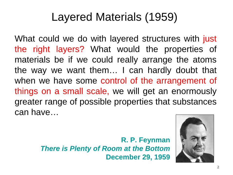
R. P. Feynman There is Plenty of Room at the Bottom
December 29, 1959
Layered Materials (1959)
What could we do with layered structures with just the right layers? What would the properties of materials be if we could really arrange the atoms the way we want them… I can hardly doubt that when we have some control of the arrangement of things on a small scale, we will get an enormously greater range of possible properties that substances can have…
3
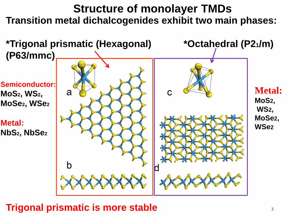
Transition metal dichalcogenides exhibit two main phases: *Trigonal prismatic (Hexagonal) *Octahedral (P21/m) (P63/mmc)
Semiconductor: MoS2, WS2, MoSe2, WSe2
Metal: NbS2, NbSe2
Metal: MoS2, WS2, MoSe2, WSe2
Trigonal prismatic is more stable 3
Structure of monolayer TMDs
4 4
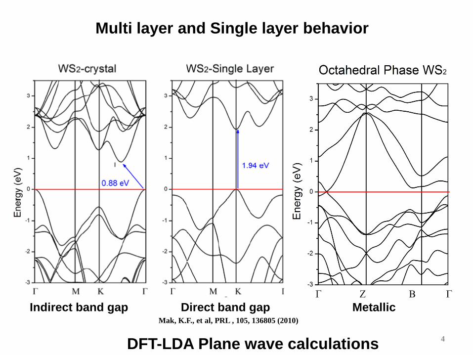
Multi layer and Single layer behavior
DFT-LDA Plane wave calculations
Indirect band gap Direct band gap Metallic Mak, K.F., et al, PRL , 105, 136805 (2010)
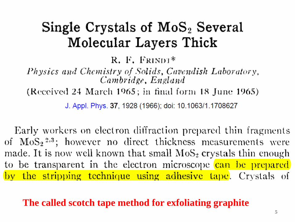
5 5 The called scotch tape method for exfoliating graphite
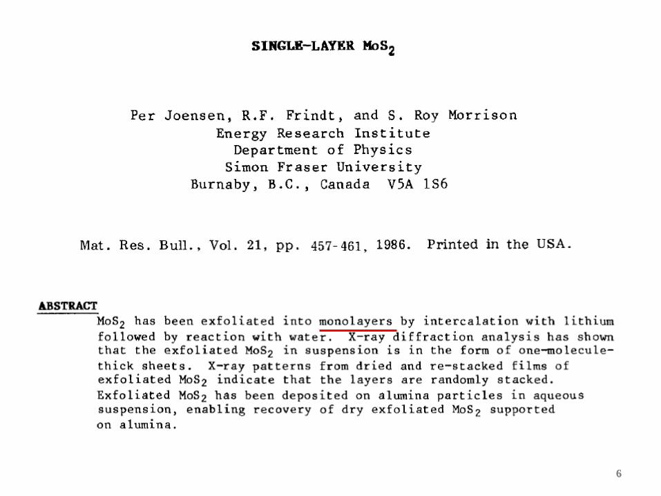
6 6
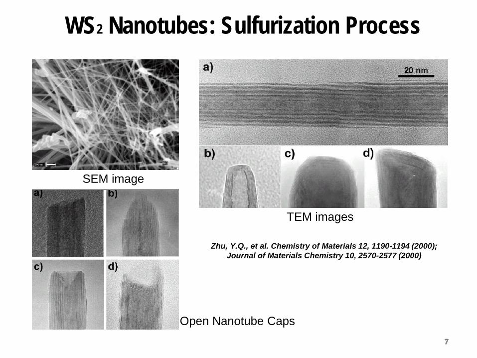
7 7 7 7 7
Zhu, Y.Q., et al. Chemistry of Materials 12, 1190-1194 (2000); Journal of Materials Chemistry 10, 2570-2577 (2000)
SEM image
TEM images
Open Nanotube Caps
WS2 Nanotubes: Sulfurization Process
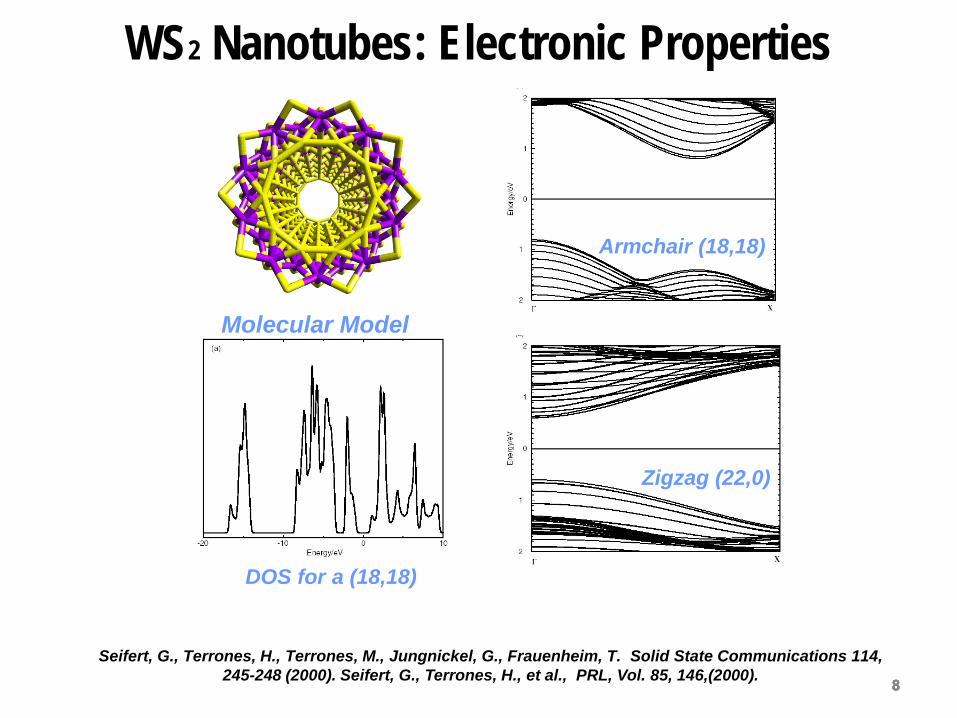
8 8 8 8 8
WS2 Nanotubes: Electronic Properties
Seifert, G., Terrones, H., Terrones, M., Jungnickel, G., Frauenheim, T. Solid State Communications 114, 245-248 (2000). Seifert, G., Terrones, H., et al., PRL, Vol. 85, 146,(2000).
Molecular Model
Armchair (18,18)
Zigzag (22,0)
DOS for a (18,18)
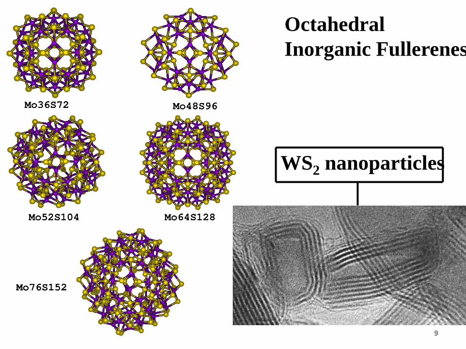
9 9 9
Octahedral Inorganic Fullerenes
WS2 nanoparticles
10 10 10 Seifert, G., Terrones, H., et al., Physical Review Letters, Vol. 85, 146(2000).
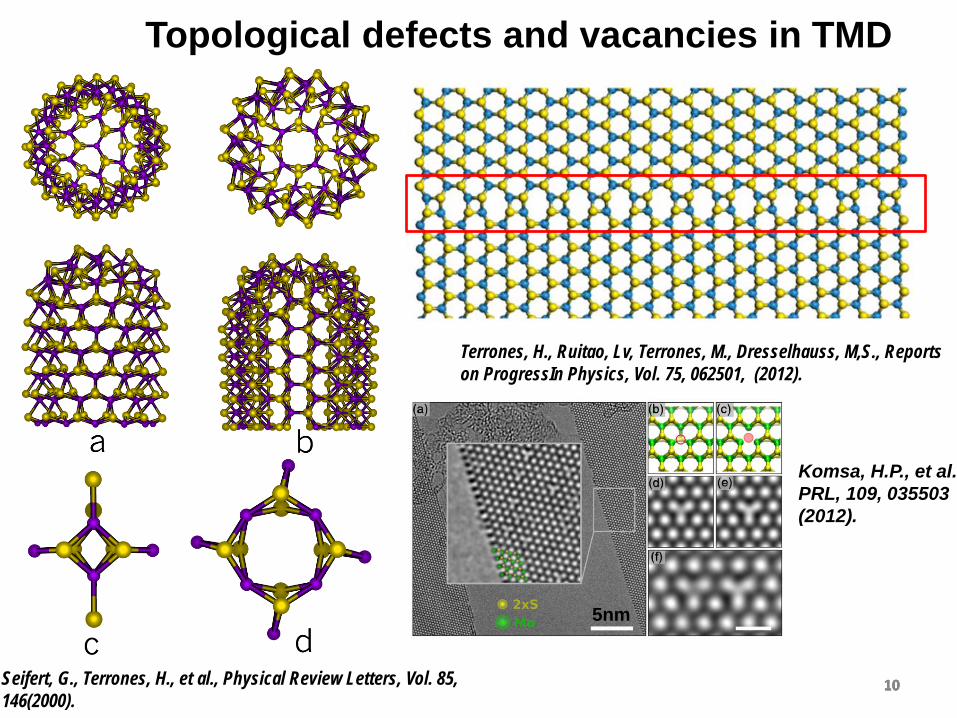
Topological defects and vacancies in TMD
Terrones, H., Ruitao, Lv, Terrones, M., Dresselhauss, M,S., Reports on ProgressIn Physics, Vol. 75, 062501, (2012).
10
Komsa, H.P., et al., PRL, 109, 035503 (2012).
5nm
11 11
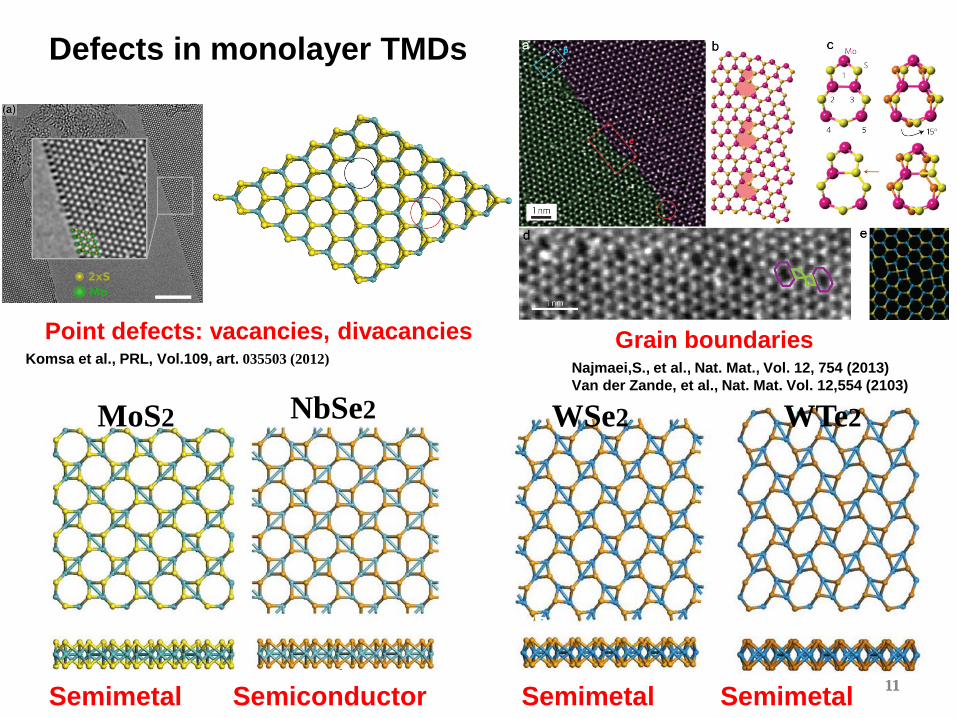
Defects in monolayer TMDs
Komsa et al., PRL, Vol.109, art. 035503 (2012) Najmaei,S., et al., Nat. Mat., Vol. 12, 754 (2013) Van der Zande, et al., Nat. Mat. Vol. 12,554 (2103)
MoS2 NbSe2
WSe2
WTe2
Semimetal Semiconductor Semimetal Semimetal
Point defects: vacancies, divacancies Grain boundaries
MoS2 NbSe2 WSe2 WTe2
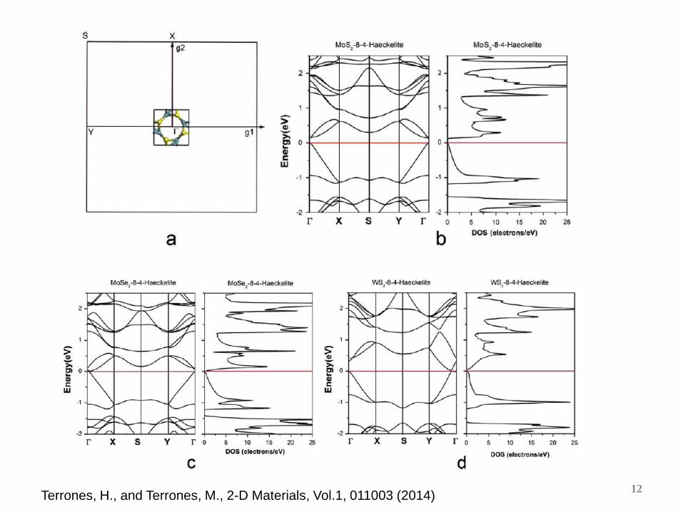
12 Terrones, H., and Terrones, M., 2-D Materials, Vol.1, 011003 (2014)
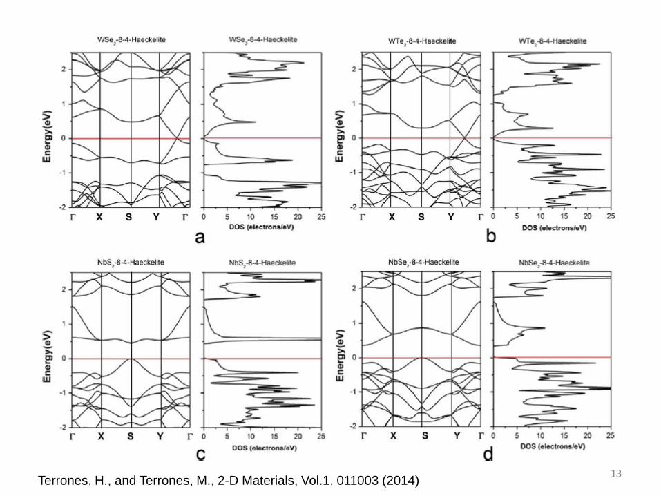
13 Terrones, H., and Terrones, M., 2-D Materials, Vol.1, 011003 (2014)
14 14
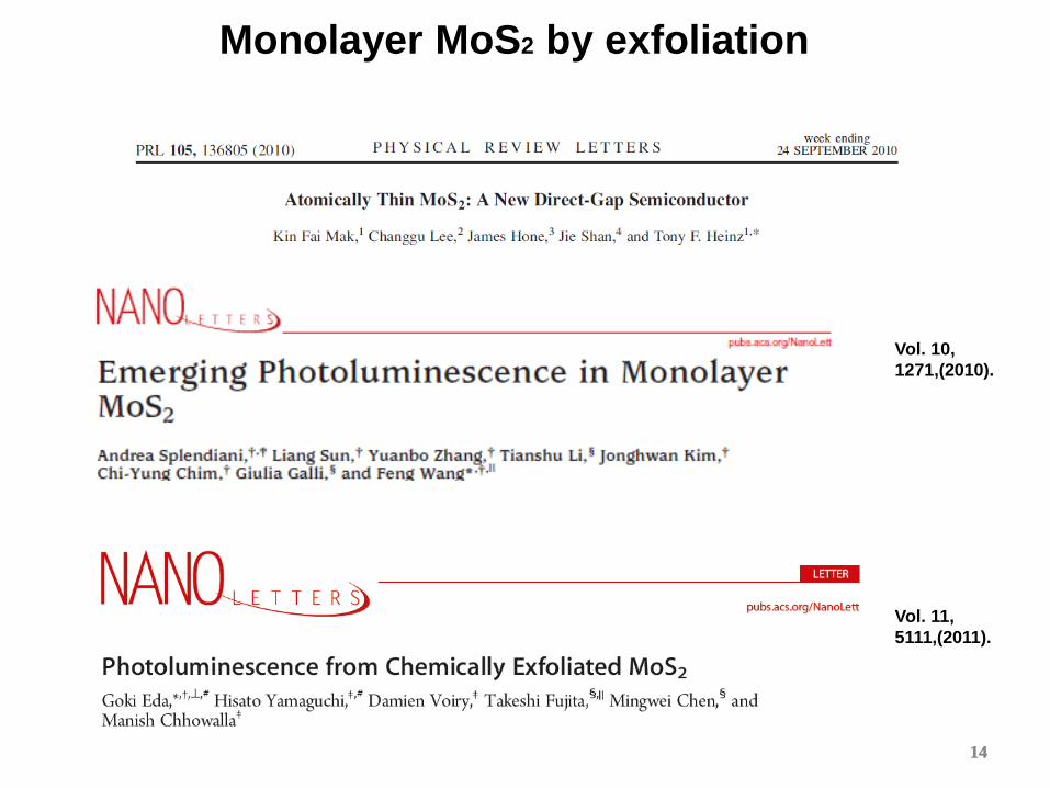
Vol. 10, 1271,(2010).
Vol. 11, 5111,(2011).
Monolayer MoS2 by exfoliation
15 15
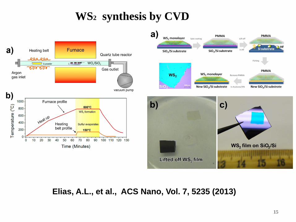
Elias, A.L., et al., ACS Nano, Vol. 7, 5235 (2013)
WS2 synthesis by CVD
16 16
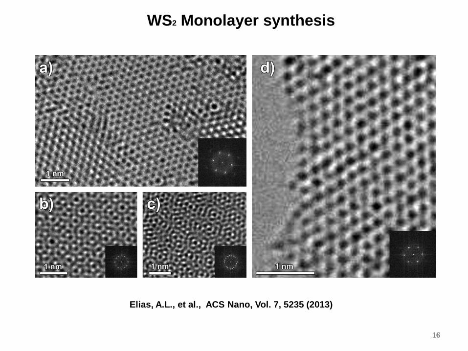
Elias, A.L., et al., ACS Nano, Vol. 7, 5235 (2013)
WS2 Monolayer synthesis
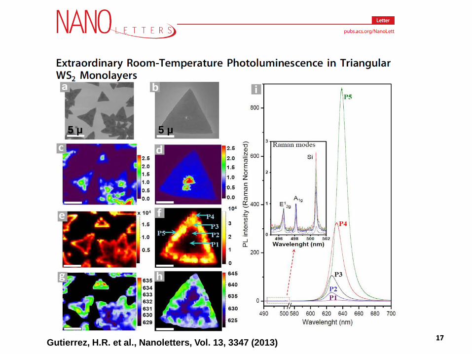
17 17 Gutierrez, H.R. et al., Nanoletters, Vol. 13, 3347 (2013)
17
5 μ
5 μ
18
Gutierrez, H.R. et al., Nanoletters, Vol. 13, 3347 (2013)
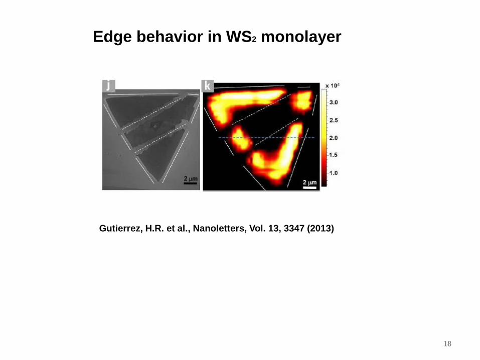
Edge behavior in WS2 monolayer
19 19 19
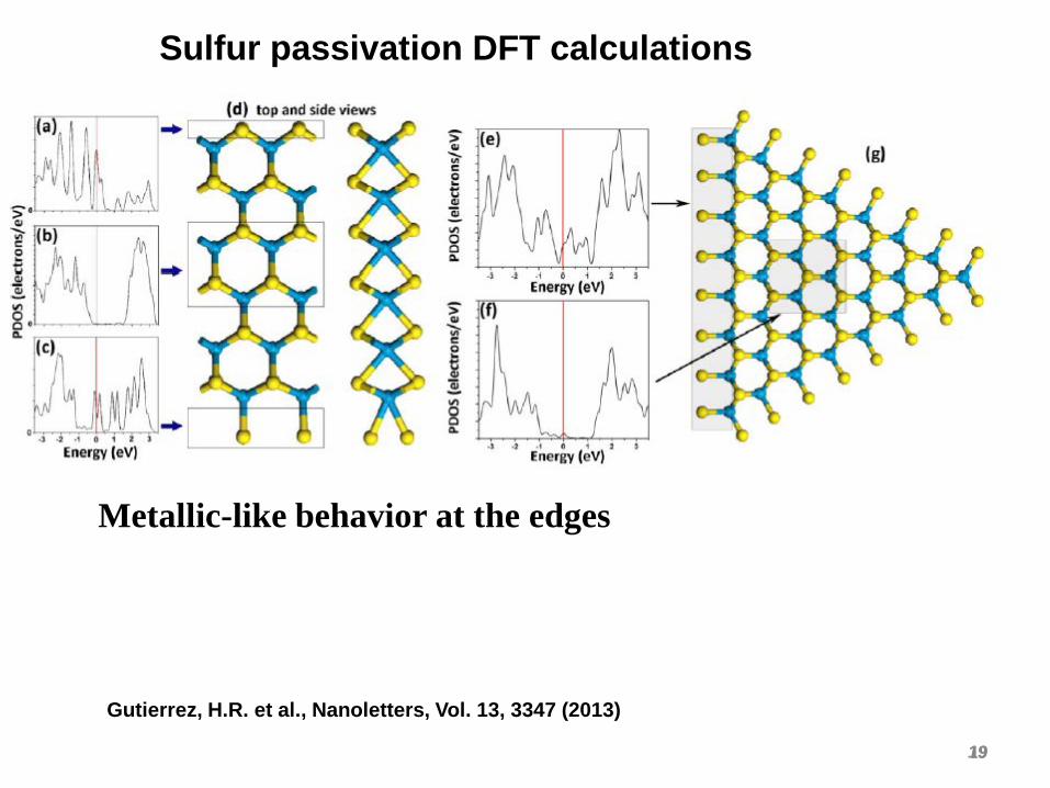
Sulfur passivation DFT calculations
Gutierrez, H.R. et al., Nanoletters, Vol. 13, 3347 (2013)
Metallic-like behavior at the edges
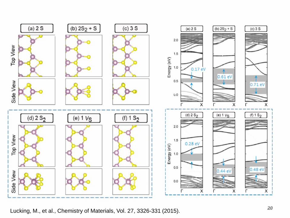
20 20 20 Lucking, M., et al., Chemistry of Materials, Vol. 27, 3326-331 (2015).
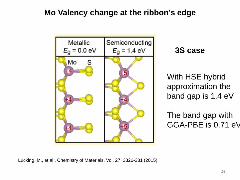
21 21 21
Mo Valency change at the ribbon’s edge
Lucking, M., et al., Chemistry of Materials, Vol. 27, 3326-331 (2015).
With HSE hybrid approximation the band gap is 1.4 eV The band gap with GGA-PBE is 0.71 eV
3S case
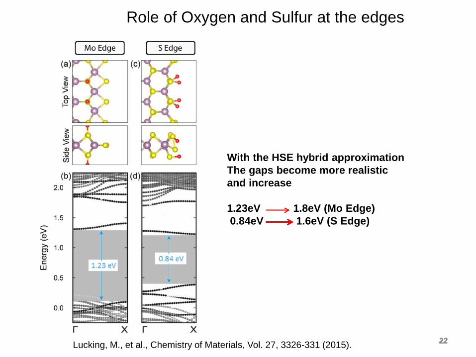
22 22 22
Role of Oxygen and Sulfur at the edges
Lucking, M., et al., Chemistry of Materials, Vol. 27, 3326-331 (2015).
With the HSE hybrid approximation The gaps become more realistic and increase 1.23eV 1.8eV (Mo Edge) 0.84eV 1.6eV (S Edge)
23 23
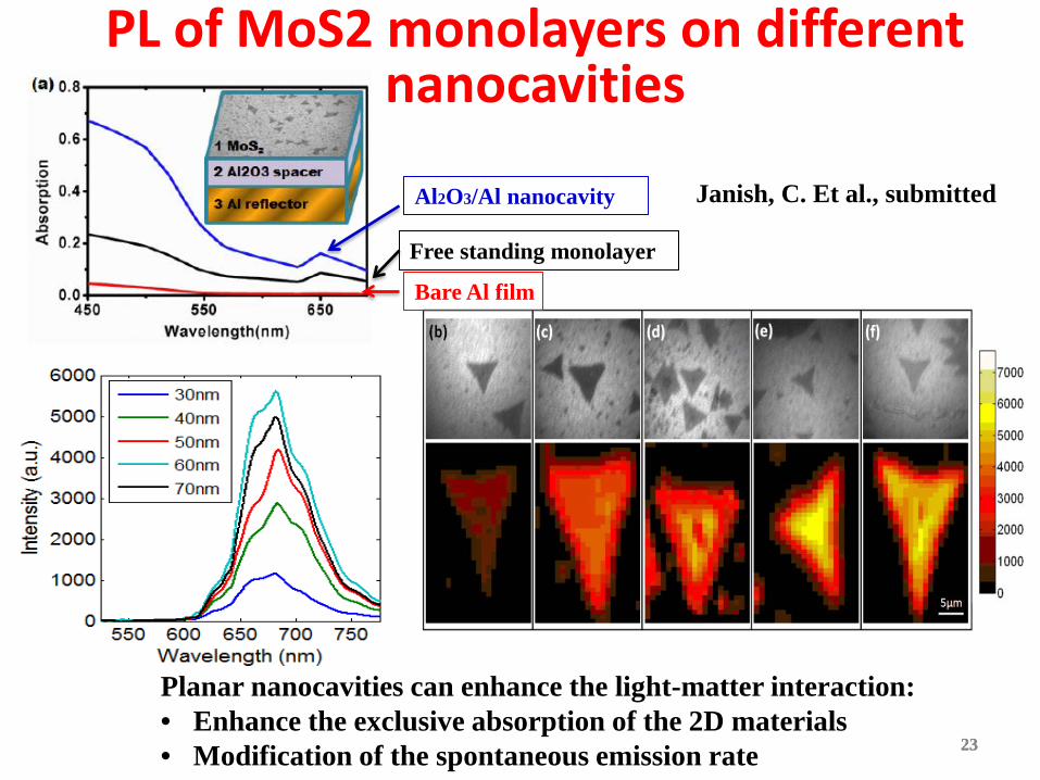
PL of MoS2 monolayers on different nanocavities
Planar nanocavities can enhance the light-matter interaction: • Enhance the exclusive absorption of the 2D materials • Modification of the spontaneous emission rate
Free standing monolayer
Bare Al film
Al2O3/Al nanocavity Janish, C. Et al., submitted
24
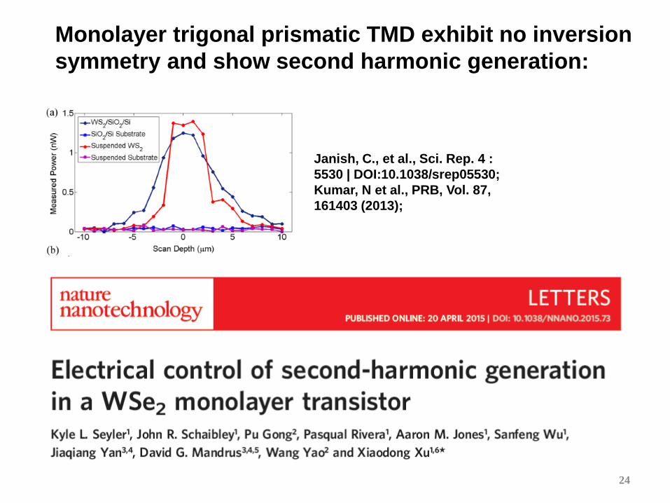
Monolayer trigonal prismatic TMD exhibit no inversion symmetry and show second harmonic generation:
Janish, C., et al., Sci. Rep. 4 : 5530 | DOI:10.1038/srep05530; Kumar, N et al., PRB, Vol. 87, 161403 (2013);
25
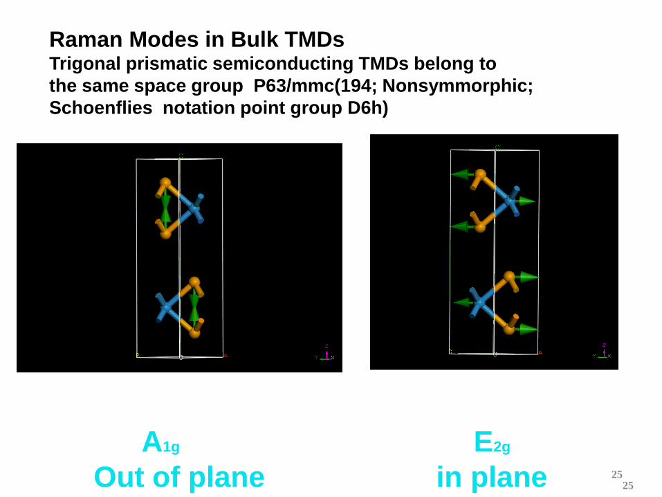
Raman Modes in Bulk TMDs Trigonal prismatic semiconducting TMDs belong to the same space group P63/mmc(194; Nonsymmorphic; Schoenflies notation point group D6h)
A1g E2g Out of plane in plane 25
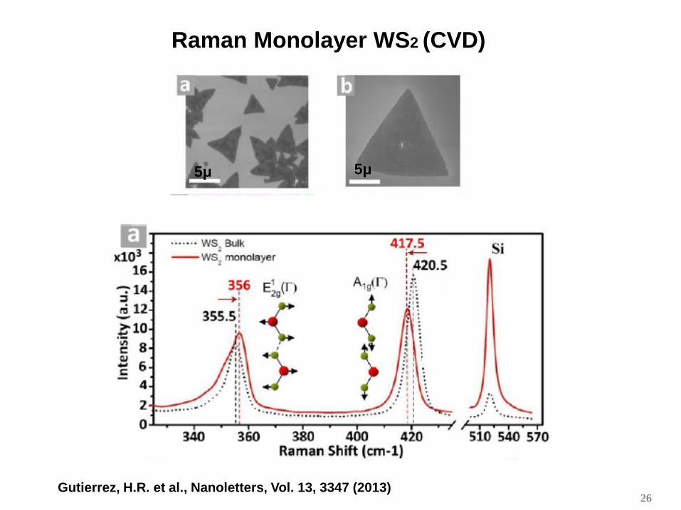
Raman Monolayer WS2 (CVD)
A’1
E’
E’ A’1
Gutierrez, H.R. et al., Nanoletters, Vol. 13, 3347 (2013)
5μ 5μ
26
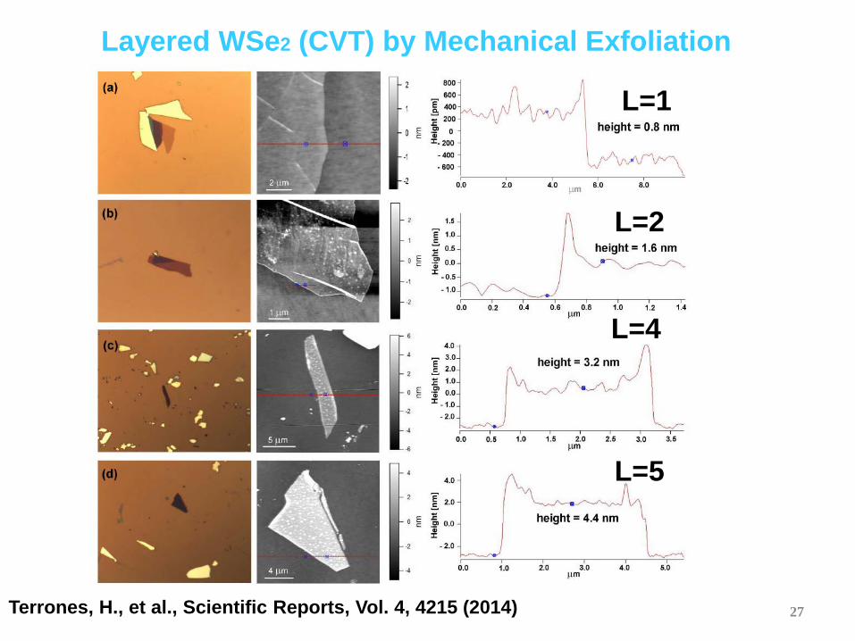
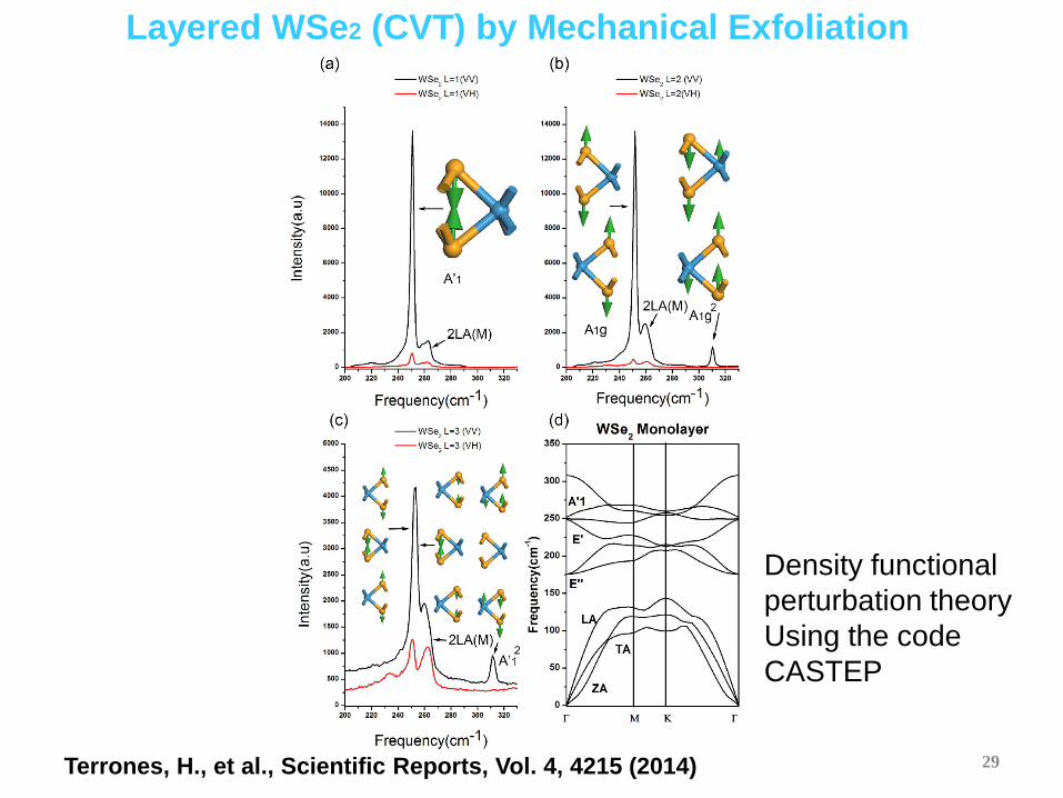
Layered WSe2 (CVT) by Mechanical Exfoliation
Terrones, H., et al., Scientific Reports, Vol. 4, 4215 (2014)
L=1
L=2
L=4
L=5
27
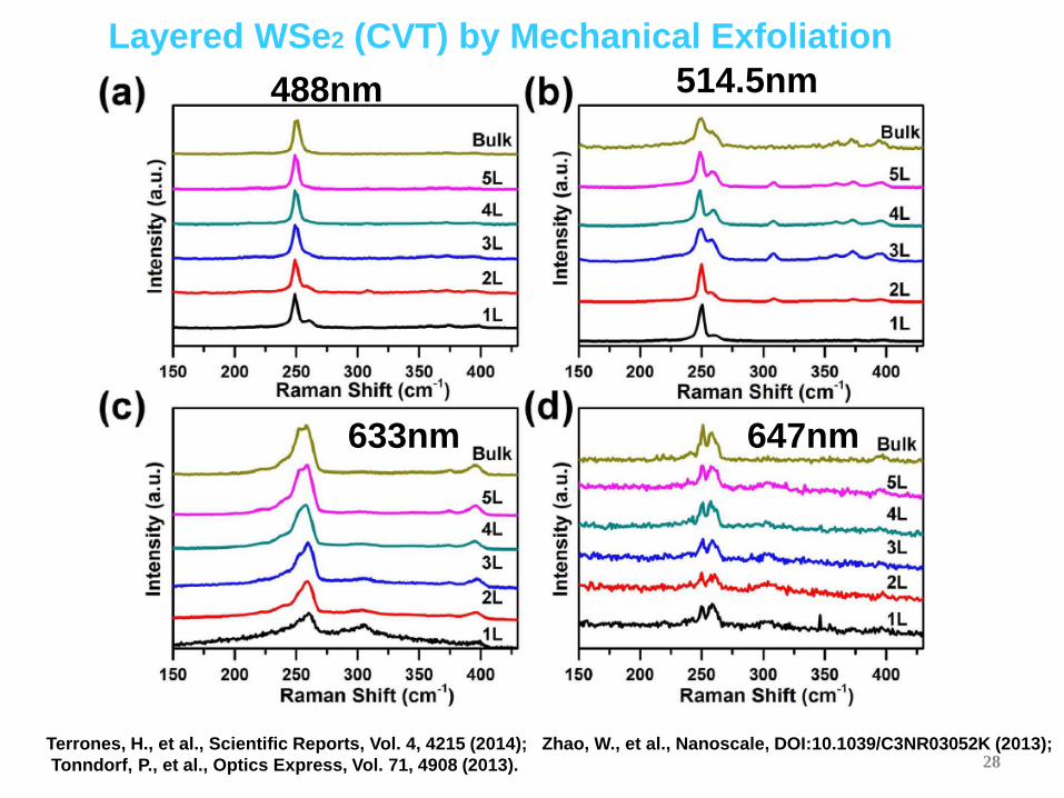
Layered WSe2 (CVT) by Mechanical Exfoliation
Terrones, H., et al., Scientific Reports, Vol. 4, 4215 (2014); Zhao, W., et al., Nanoscale, DOI:10.1039/C3NR03052K (2013); Tonndorf, P., et al., Optics Express, Vol. 71, 4908 (2013).
488nm 514.5nm
633nm
647nm
28
488nm 514.5nm
514.5nm
Terrones, H., et al., Scientific Reports, Vol. 4, 4215 (2014)
Layered WSe2 (CVT) by Mechanical Exfoliation
Density functional perturbation theory Using the code CASTEP
E’
Eg
29
30 30
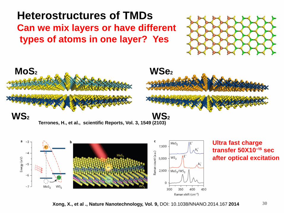
Heterostructures of TMDs Can we mix layers or have different types of atoms in one layer? Yes
MoS2
WS2 WS2
WSe2
Xong, X., et al ., Nature Nanotechnology, Vol. 9, DOI: 10.1038/NNANO.2014.167 2014
Ultra fast charge transfer 50X10⁻¹⁵ sec after optical excitation
MoS2 WS2
Terrones, H., et al., scientific Reports, Vol. 3, 1549 (2103)
31 31
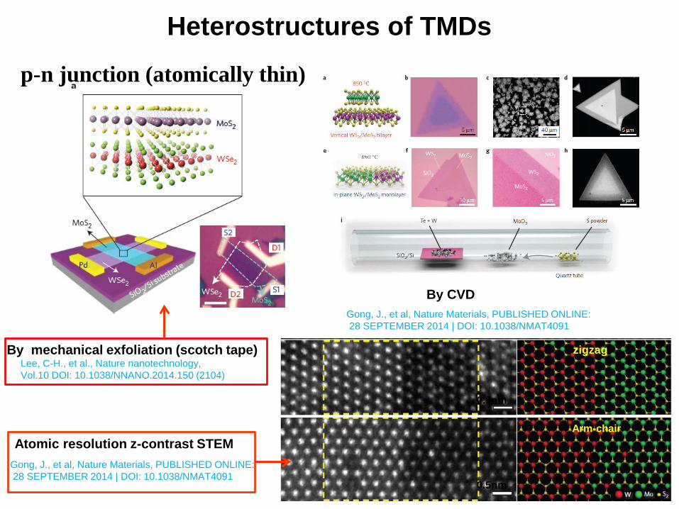
Heterostructures of TMDs
Atomically thin p-n junctions
Lee, C-H., et al., Nature nanotechnology, Vol.10 DOI: 10.1038/NNANO.2014.150 (2104)
Gong, J., et al, Nature Materials, PUBLISHED ONLINE: 28 SEPTEMBER 2014 | DOI: 10.1038/NMAT4091
By mechanical exfoliation (scotch tape)
By CVD Gong, J., et al, Nature Materials, PUBLISHED ONLINE: 28 SEPTEMBER 2014 | DOI: 10.1038/NMAT4091
Atomic resolution z-contrast STEM
0.5nm
0.5nm
zigzag
Arm-chair
p-n junction (atomically thin)
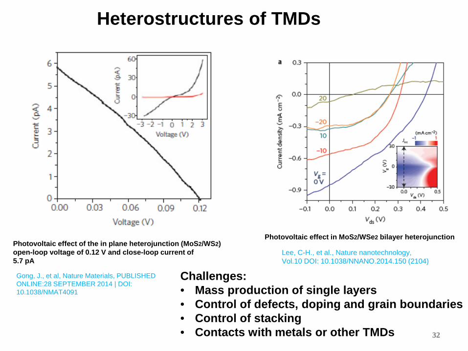
32 32
Photovoltaic effect of the in plane heterojunction (MoS2/WS2) open-loop voltage of 0.12 V and close-loop current of 5.7 pA
Heterostructures of TMDs
Gong, J., et al, Nature Materials, PUBLISHED ONLINE:28 SEPTEMBER 2014 | DOI: 10.1038/NMAT4091
Challenges: • Mass production of single layers • Control of defects, doping and grain boundaries • Control of stacking • Contacts with metals or other TMDs
Photovoltaic effect in MoS2/WSe2 bilayer heterojunction
Lee, C-H., et al., Nature nanotechnology, Vol.10 DOI: 10.1038/NNANO.2014.150 (2104)
Acknowledgements: NSF (EFRI-1433311), U.S. Army Research Office MURI grant W911NF-11-1-0362,Penn State Center for Nanoscale Science Seed grant on 2-D Layered Materials (DMR-0820404).
33

Thank you
34