BenQ G610HDA_V1
47
1 Product Service Manual Service Manual for BenQ: G610HDA P/N: 9H.L06LN.IXX Applicable for All Regions Version: 001 Date:2008/12/24 Notice: - For RO to input specific “Legal Requirement” in specific NS regarding to responsibility and liability statements. - Please check BenQ’s eSupport web site, http://esupport.benq.com , to ensure that you have the most recent version of this manual. First Edition (July, 2008) © Copyright BenQ Corporation 2008. All Right Reserved.
Transcript of BenQ G610HDA_V1
1
Product Service Manual
Service Manual for BenQ:
G610HDA
P/N: 9H.L06LN.IXX
Applicable for All Regions
Version: 001
Date:2008/12/24
Notice:
- For RO to input specific “Legal Requirement” in specific NS regarding to responsibility and liability statements.
- Please check BenQ’s eSupport web site, http://esupport.benq.com, to ensure that you have the most recent
version of this manual.
First Edition (July, 2008)
© Copyright BenQ Corporation 2008. All Right Reserved.

2
Content Index
1. About This Manual ..............................................................................................................................................3
1.1 Trademark......................................................................................................................................................... 3
2. Precautions & Safety Notices .............................................................................................................................4
2.1 Safety Precaution ............................................................................................................................................. 4
2.2 Product Safety Notice ....................................................................................................................................... 4
2.3 Service Notes.................................................................................................................................................... 4
3. Product Overview................................................................................................................................................5
3.1 Power Supply.................................................................................................................................................... 5
3.2 Signal Interface................................................................................................................................................. 5
3.3 Scan Range ...................................................................................................................................................... 6
3.4 Support Timings................................................................................................................................................ 6
3.5 Operational & Function Specification................................................................................................................ 9
3.6 LCD Characteristics........................................................................................................................................ 11
3.7 User Controls .................................................................................................................................................. 11
3.8 Mechanical Characteristics............................................................................................................................. 12
3.9 Pallet & Shipment ........................................................................................................................................... 13
4 Level 1 Cosmetic / Appearance / Alignment Service .........................................................................................13
4.1 Software / Firmware Upgrade Process........................................................................................................... 14
4.2 Alignment Procedure (for function adjustment) .............................................................................................. 14
5. Level 2 Disassembly/Assembly/Circuit Board/Standard Parts Replacement ...................................................19
5.1 Exploded Diagram .......................................................................................................................................... 19
5.2 Assembly Block............................................................................................................................................... 20
5.3 Disassembly Block.......................................................................................................................................... 25
5.4 Block Diagram................................................................................................................................................. 29
5.5 Lay out ............................................................................................................................................................ 34
5.6 Trouble Shooting Guide .................................................................................................................................. 41
6. Dimension Drawing...…………………………………………………………………………………………………48
3
1. About This Manual
This manual contains information about maintenance and service of BenQ products. Use this manual to
perform diagnostics tests, troubleshoot problems, and align the BenQ product.
1.1 Trademark
The following terms are trademarks of BenQ Corporation:
BenQ
Importance
Only trained service personnel who are familiar with this BenQ Product shall perform service or maintenance
to it. Before performing any maintenance or service, the engineer MUST read the “Safety Note”

4
2. Precautions & Safety Notices
2.1 Safety Precaution
This monitor is manufactured and tested on a ground principle that a user’s safety comes first. However,
improper used or installation may cause damage to the monitor as well as to the user.
WARNINGS:
This monitor should be operated only at the correct power sources indicated on the label on the rear of the monitor. If you’re unsure of the power supply in you residence, consult your local dealer or Power Company.
Do not try to repair the monitor by yourself, as it contains no user-serviceable parts. This monitor should only be repaired by a qualified technician.
Do not remove the monitor cabinet. There is high-voltage parts inside that may cause electric shock to human bodies.
Stop using the monitor if the cabinet is damaged. Have it checked by a service technician. Put your monitor only in a lean, cool, dry environment. If it gets wet, unplug the power cable immediately
and consult your closed dealer. Always unplug the monitor before cleaning it. Clean the cabinet with a clean, dry cloth. Apply
non-ammonia based cleaner onto the cloth, not directly onto the class screen. Do not place heavy objects on the monitor or power cord.
2.2 Product Safety Notice
Many electrical and mechanical parts in this chassis have special safety visual inspections and the protection afforded by them cannot necessarily be obtained by using replacement components rated for higher voltage, wattage, etc. Before replacing any of these components read the parts list in this manual carefully. The use of substitute replacement parts, which do not have the same safety characteristics as specified in the parts list, may create shock, fire, or other hazards.
2.3 Service Notes
When replacing parts or circuit boards, clamp the lead wires around terminals before soldering.
Keep wires away from high voltage, high temperature components and sharp edges.
Keep wires in their original position so as to reduce interference.
Adjustment of this product please refers to the user’ manual.

5
3. Product Overview
3.1 Power Supply
Items Condition Spec Note
AC Input Voltage Range Universal input full range 100~240VAC /50~60Hz
AC Input Current 100Vac 240Vac
1.0A(max) 0.5A(max)
AC Frequency Range 100Vac 240Vac
50Hz – 60Hz
Inrush Current
120Vac,cold star,0°C 240Vac,cold star,0°C
30A (max) 60A(max)
Regulator Efficiency DC output full loading ≥75%
Ripple and Noise ---- ---- See Note4
+5.2Vcc output <150mV(Brightness is 100%); <250mV(Brightness is 0%.);
DC Output Voltage
VCC14.2V(13.5~16.3V)VCC5.2V(4.95~5.45V)
0.8A(typ.),1.0A(max) 0.8A(typ.),1.0A(max)
See Note 2
Power consumption without Audio ≤18W
Protection See Table-1
Power management See Table-2Note2. For the normal loading test ,the output loading use typical current.
Note4. Tested by DC loading side parallel with a 47uF/EC and 0.1uF/Ceramic , Capacitors and measured
band-width with DC-20MHz, the sine wave signal that the frequency is 1K Hz input when testing the ripple for
the 5V of audio.
3.2 Signal Interface
Input Connector Analog : D-sub 15
Default Input Connector D-sub
Video Cable Strain Relief Equal to twice the weight of the monitor for five
minutes
Video Cable Connector DB-15 Pin out Compliant DDC 2B / CI
Video Signals Video RGB (Analog): Separate
Video Impedance 75 Ohms (Analog)
Maximum PC Video Signal 950 mV with no damage to monitor
Maximum Mac Video Signal 1250 mV with no damage to monitor
Sync Signals TTL
DDC 1/2B Compliant with Revision 1.3
Sync Compatibility Separate Sync/Composite Sync
Video Compatibility Shall be compatible with all PC type computers,
Macintosh computers, and after market video cards

6
3.3 Scan Range
Item condition Spec OK NA Remark
Horizontal
Sync polarity: (+) or (-)
30~63 KHz
√
Vertical
Sync polarity: (+) or (-) 50~76Hz
√
3.4 Support Timings BenQ customer preset Tmings are as below:
P: Preset Mode NP: Non Preset Mode FS: Fail Save Mode(show “Out of Range”, but still can see picture) O: Out of Range(only show “Out of Range”, without picture )
No. Resolution Pixel clock H-sync V-sync H-Pol V-Pol
1 640x350 25.18 31.47 70.09 + - FS
2 640x350 31.5 37.86 85.08 + - O
3 640x400 25.18 31.47 70.09 - + FS
4 640x400 31.5 37.86 85.08 - + O
5 640x480 30.24 35 66.67 - - NP
6 640x480 25.17 31.47 59.94 - - P
7 640x480 31.5 37.86 72.81 - - FS
8 640x480 31.5 37.5 75 - - FS
9 640x480 36 43.27 85.01 - - O
10 640x500 25.25 31 57.76 - - NP
11 720x400 28.32 31.47 70.08 - + FS
12 720x400 35.5 37.93 85.04 - + O
13 832x624 57.27 49.71 74.53 - - FS
14 800x600 36 35.16 56.25 + + NP
15 800x600 40 37.88 60.32 + + P
16 800x600 50 48.08 72.19 + + FS
17 800x600 49.5 46.88 75 + + FS
18 800x600 56.25 53.67 85.06 + + FS
19 848x480 33.75 31.02 60 + + NP
20 848x480 31.5 29.83 59.66 - + NP
21 848x480 37.52 35 70 - + NP
22 848x480 39.25 36.07 72 - + NP
23 848x480 41 37.68 74.77 - + FS
24 720x576 32.71 35.91 59.95 - + NP

7
25 1024x768-I 44.9 35.52 43.48 + + FS
26 1024x768 65 48.36 60 - - P
27 1024x768 75 56.48 70.07 - - NP
28 1024x768 78.43 57.67 72 - + NP
29 1024x768 80 60.24 74.93 - - FS
30 1024x768 78.75 60.02 75.03 + + FS
31 1024x768 94.5 68.68 85 + + FS
32 1152x720 66.75 44.86 60 - + P
33 1152x864 94.5 63.85 70.01 + + FS
34 1152x864 108 67.5 75 + + FS
35 1152x864 119.651 77.09 85 - + FS
36 1152x870 100 68.68 75.06 - - FS
37 1152x900 92.94 61.8 65.95 - - FS
38 1152x900 105.59 71.73 76.07 - - FS
39 1280x720 74.25 45 59.94 - + P
40 1280x720 74.5 44.77 59.86 - + P
41 1280x720 95.75 56.46 74.78 - + FS
42 1280x768-R 68.25 47.4 60 + - P
43 1280x768 79.5 47.78 59.87 - + P
44 1280x768 102.25 60.29 74.89 - + FS
45 1280x768 117.5 68.63 84.84 - + FS
46 1280x800 71 49.31 59.91 + + FS
47 1280x800 83.5 49.702 59.81 - + FS
48 1280x800 88.25 58.3 70 - + FS
49 1280x800 102.8 60.048 72 - + FS
50 1280x800 106.6 62.795 74.934 - + FS
51 1280x800 122.5 71.55 84.88 - + FS
52 1280x960 108 60 60 + + FS
53 1280x960 148.5 85.94 85 + + FS
54 1280x1024 108 63.98 60.02 + + FS
55 1280x1024 126.99 74.88 69.85 + + FS
56 1280x1024 124.9 74.4 70 - - FS
57 1280x1024 134.6 77.9 72 + + FS
58 1280x1024 135 79.98 75.02 + + FS
59 1280x1024 135.09 81.18 76.16 - - FS
60 1280x1024 157.5 91.15 85.02 + + O

8
61 1360x768 85.5 47.71 60.01 + + P
62 1366x768 85.5 47.71 59.79 + + P
63 1400x1050-R 101 64.74 59.95 + - FS
64 1400x1050 121.75 65.32 59.98 - + FS
65 1400x1050 156 82.28 74.87 - + O
66 1400x1050 179.5 93.88 84.96 - + O
67 1440x900-R 88.75 55.496 59.901 + - FS
68 1440x900 106.5 55.935 59.887 - + FS
69 1440x900 136.75 70.6 75 - + FS
70 1600X900 97.75 59.75 55.54 + - FS
71 1600x1000-R 108.5 61.648 59.91 + - FS
72 1600x1000 132.25 62.14 59.87 - + FS
73 1600x1000 169.25 78.356 74.83 - + O
74 1600x1200-R 130.25 74.01 59.92 + - FS
75 1600x1200 162 75 60 + + O
76 1600x1200 175.5 81.25 65 + + O
77 1600x1200 189 87.5 70 + + O
78 1600x1200 202.5 93.75 75 + + O
79 1600x1200 229.5 106.25 85 + + O
80 1680x1050-R 119 64.67 59.88 + - FS
81 1680x1050 146.25 65.29 59.95 - + O
82 1680x1050 187 82.306 75 - + O
83 1600x1280 171.75 79.5 59.9 - + O
84 1792X1344 203.25 83.57 59.9 - + O
85 1792X1344 257.75 105.29 75 - + O
86 1856X1392 217.25 86.485 59.934 - + O
87 1856X1392 277.5 109 74.918 - + O
88 1800x1440 218.25 89.4 59.9 - + O
89 1920x1080-R 138.5 66.587 59.934 + - O
90 1920x1080 173 67.158 59.963 - + O
91 1920x1080 148.5 67.5 60 + + O
92 1920X1200-R5 127.75 61.418 49.974 + - FS
93 1920X1200-R 154 74.04 59.95 + - O
94 1920X1200 193.25 74.56 59.89 - + O
95 1920X1200 245.25 94.04 74.93 - + O
96 1920X1440-R 184.75 88.822 59.9 + - O

9
97 1920X1440 233.5 89.532 59.968 - + O
98 1920X1440 298 112.5 74.9 - + O
99 2048x1152-R 156.75 70.992 59.9 + - O
100 2048x1152 197 71.584 59.9 - + O
101 2048x1536-R 209.25 94.7 59.9 + - O
102 2048x1536 267.25 95.4 59.9 - + O
103 2560x1600-R 268.5 98.713 59.972 + - O
104 2560x1600 348.5 99.4 59.9 - + O
Remark :
default mode : 1366x768 @ 60Hz
3.5 Operational & Function Specification
3.5.1 Video Performance
* All Spec. of monitor need to warm up at lease 1hr
Features Specifications
Maximum resolution 1366x768 @ 60Hz
Back light system 2 CCFLs
Actual Resolution display WUXGA (1366x768)
Pixel pitch 0.252 (per one triad) x 0.252
Display area 344.23 (H) x 193.54 (V)
Contrast ratio/ For CMO Panel: 3501׃ (min.), 5001׃ (Typ.)
Dynamic contrats ratio(typ) DCR :7500:1(Min) 10000:1(typ)
Brightness 210 nits (min) 250 nits (Typ)---For CMO Panel
Response time (Tr +Tf ) AUO Panel: 8ms (Typ.) 16ms (Max.)
NTSC ratio 65%
Viewing angle (H/V) 45/45; 20/45
Input interface Analog (D-sub 15 pin)
Power management Compatible with Energy Star, DPMS
Plug & Play VESA DDC2B / CI
University AC power supply 100V – 240VAC, 50Hz – 60Hz
OSD language 17 Languages (English / Francais / Deutsch / Italiano / Espanol / Polish / Czech / Hungarian / Serbo-croatian / Romanian / Netherlands / Russian / Swedish / Protuguese / Japanese / Chinese / S-Chinese)
3.5.2 Brightness Adjustable Range
The test to verify specifications in this section shall be performed under the following standard
conditions unless otherwise noted.

10
Temperature : 25 ± 5°C Test pattern : white Video Resolution : 1366 x 768@60HZ Video input level : 700 mV ± 2% Warm-up time : 30 minutes
Item Condition SPEC
Brightness=0%
Contrast = 0%
NA
Brightness=100%
Contrast = 100%
≥ 210 cd/m2
Brightness=90%
Contrast = 50%
Luminance Range
NA
3.5.3 Environment
Operating Specification Temperature range 0°C to 40°C
Relative humidity 20% to 90%
Altitude 0 to 10000 feet
Storage
Temperature range -20°C to 60°C
Relative humidity 10% to 90%
Altitude 0 to 40000 feet
3.5.4 Speaker(NA)
Speaker : 1.5W 12Ω X 2
Input impedance : ≥ 10K ohm
Frequency response range : 500Hz – 20kHz
Signal to noise ratio : ≥ 70 dB
Output power: 1.0 W + 1.0 W (Typical) @10%THD (Input sine wave signal:1KHz/0.7Vrms)
3.5.5 Electrostatic discharge Requirements
Item Condition Spec Remark Contact discharge : 4KV Contact discharge : 8KV
Air discharge : 8KV
Electrostatic
Discharge InnoLux SPEC
Air discharge : 15KV
D-sub cable pin
need test 8KV

11
3.5.6 Reliability
Items Condition Spec Note
MTBF 95% Confidence ≧ 60,000 Hours
CCFL Life time Luminance becomes 50% ≧ 40,000 Hours at 7.5mA
(min)
Note1
Note1. Display an all white field at mid Brightness and Contrast settings.
3.5.7 Audio performance (NA)
Items Specification
Speaker 1.5W 12Ω X 2Input impedance ≥ 10K ohmFrequency response range 500Hz – 20kHz
Signal to noise ratio ≥ 70 dB
Output power 1.0 W + 1.0 W (Typical) @10%THD (Input sine wavesignal:1KHz/0.7Vrms)
3.6 LCD Characteristics
The physical definition &technology summary of LCD panel
Supplier CMO
Model name M156B1-L01
Display Area 344.232 (H) x 193.536 (V)
Pixel Pitch 0.252(H) x 0.252(V)
Display Colors 16.7M(6 Bit+Hi-FRC)
Number of Pixel 1,366(H) X 768(V),
Brightness 210cd/m2 (Min.), 250cd/m2 (Typical)
Min: 350:1 Contrast Ratio
Typical: 500:1
Hor+: 45°, Hor-:45°
Viewing Angle Ver+: 20° ,Ver-:45°(Typical, CR>10)
Display Mode Normally White
Frame rate 40~76Hz
Response Time 8 ms (Typical), 16ms (Max.)
Surface Treatment Anti-glare type, Hardness 3H
Lamp 2 CCFLs
Outline Dimension 363.8(W) x 215.9(H) x 14.3(D) (Typ)
3.7 User Controls
User’s hardware control definition:

12
3.8 Mechanical Characteristics
3.8.1Dimension
Item condition Spec OK NA Remark
Bezel opening Lx W 377.8x300.95mm √
Monitor without stand L×W×Hmm 377.8*55.35*240.12mm √
Monitor with stand L×W×Hmm 377.8*146*300.95mm √
Carton Box(outside) L×W×Hmm 442x116x354mm √
Tilt and Swivel range Tilt:-5~23degree
Swivel: 0 degree
√
3.8.2 Weight
Item condition Spec OK Remark
Monitor (Net) 2.35±0.5 Kg ( Net )
Monitor with
packing(Gross) 3.35±0.5Kg( Gross / with packing )
3.8.3 Plastic
Item condition Spec OK NA Remark
Flammability 94-HB √
Heat deflection to 80°C √
UV stability Delta E<12 √
Resin ABS √
Texture GLOSS2000
拋光
MT10010
MT10020
√ 1.BEZEL: MT-11010
2. BACKCOVER: MT-11020
3. STAND BACK COVER: MT-11010
4. STAND FRONT COVER: MT-11010
5. FUNCTION KEY: MT-11010
6. LED LENS: MT-11010
7. CLIP:共用 BenQ G900
8. HINGE COVER:MT-11010
9.LOGO BACK COVER:GLOSS2000
10. BASE:MT-11010
Color BCS-Y7015A
(Black)
√
3.8.4 Carton
Carton:Item condition Spec OK NA Remark
Color

13
3.9 Pallet & Shipment
3.9.1 Container Specification
Stowing Type Containter Quantity of
Produces (sets)
(Every container)
Quantity of
Produces (sets)
(Every Pallet)
Quantity of Pallet
(sets)
(Every container)
20’SEA
1440 Pallet A: 120
Pallet B:X
Pallet A:12
Pallet B:X
40’SEA 3120 Pallet A: 120
Pallet B:X
Pallet A:26
Pallet B:X
20’AIR 864 Pallet A: 72
Pallet B:X
Pallet A:12
Pallet B:X
With Pallet
(C Flute)
40’AIR 1872 Pallet A: 72
Pallet B:X
Pallet A:26
Pallet B:X
20’SEA 1344 Pallet A: 112
Pallet B:X
Pallet A:12
Pallet B:X
With Pallet
(A Flute)
40’SEA 2912 Pallet A: 112
Pallet B:X
Pallet A:26
Pallet B:X
3.9.2 Carton Specification
Product:
Net Weight (Kg) Gross Weight(Kg) Dimension w/o Base
LxWxH (mm)
Dimension w/ Base
LxWxH (mm)
2.35±0.5 Kg ( Net) 3.35±0.5Kg 377.8*55.35*240.12mm 377.8*146*300.95mm
3.9.3 Package:
Items Spec
Packaging Refer to ME PACKING SPEC
Ink The ink shall not rub off after a suitable drying time
Shipping Carton Type One Piece Construction Shipping Carton Handholds Yes Length 444mm Height 350mm Width 114mm Gross Weight 3.21kg+/-0.5
Units per Pallet 120sets / pallet A
Material C Flute √ A Flute For Japan
Compression strength 200 KGF √ 250 KGF For Japan
Burst strength 16 KGF/cm2 √ 19.4 KGF/cm2 For Japan
Stacked quantity 6 Layers √ 5 Layers

14
4 Level 1 Cosmetic / Appearance / Alignment Service
4.1 Software / Firmware Upgrade Process
Upload firmware to Flash ROM via VGA Cable
1. Connect ISP board between monitor and PC as below configuration.
2. Select the Flash ROM type which is used in this monitor, then select the ISP button, and then choose
corresponding firmware, and load them to Flash ROM.
4.2 Alignment Procedure (for function adjustment)
4.2.1 Preparation:
1. Setup input timing VESA to 1366*768@60Hz,32-Grays pattern.
2. Setup units and keep it warm up for at least 30 minutes.
4.2.2 Timing adjustment
1. Enter to factory mode setting area (by pressing "ENTER"+ "MENU" + "POWER" at the same time during
power off).
2. Check the settings to following values:
contrast =50;
brightness=90;
3. Then turn off the monitor power.
4.2.3 Function key Definitions
4.2.3.1 Control buttons on the rear side of monitor
CONTROL KEY KEYS FUNCTION
[MENU]
A. When OSD displays, press [MENU] to return to previous level menu B. When OSD isn’t shown on screen, press [MENU] to enter OSD interface C. Press [MENU] to enter Service Page When OSD isn’t shown on screen in Service
Page Mode
[Enter] A. When OSD displays, press [Enter] to perform function of menu icon that is highlight or enter next level menu
Insert to Parallel
Port on PC
ISP Board
LCD Monitor
D-Sub
Parallel
Port
D-SU
B

15
[], []
A. When “MENU OSD” displays, press these keys to change the contents of an adjustment item, or change an adjustment value
B. When “MENU OSD” un-displays, press []Brightness and contrast. press [](down) to Show Picture Mode Menu.
[POWER] Power on or power off the monitor
[Auto] press [Auto] to perform auto-adjustment
4.2.3.2HOT KEY OPERATION
HOT KEY OPERATION FUNCTION MENU Enter AUTO POWER
DESCRIPTION
FACTORY MODE
Press[MENU], [Enter]& [POWER] at
the same time, when Monitor is Power
On OSD menu will be shown with “F”
on the left top. Select “F” for entering
factory mode.
Picture Mode To Show & Change Picture Mode Menu
Brightness/Contrast To show the Brightness/Contrast Menu
Auto Adjustment press [AUTO] to process, Auto Adjustment
Service Page Press [MENU] + [POWER] to Enter Service Page Mode when power off
Input Source Press [Enter] to change Input Source when OSD isn’t Display.
Note: Picture Mode Standard <( Movie <( Dynamics <( Photo <( sRGB <( Standard
Auto Power on/off function in service mode:
Default is “off”, Monitor will remember the last status before AC off. And monitor would always be off while AC off->on in “off” mode.
4.2.4 OSD Control
The On-Screen Display (OSD) shall be an easy to use icon based menu through keypad OSD buttons or remote control unit. The unit shall leave the factory with all OSD controls set to their default values.
First level Second level Third level Fourth level Default
Auto Adjustment - - -
H. Position (0~100) - 50
V. Position (0~100) - 50
Pixel Clock (0~100) - 50
DISPLAY
Phase (0~63) - -

16
Brightness (0~100) - 90
Contrast (0~100) - 50
Sharpness (1~5) - 3
Normal Normal
Bluish -
Reddish - *Color
temperature User Mode
Red (0~100)
Green (0~100)
Blue (0~100)
100
Color
Reset Color (YES/NO)
PICTURE
Dynamic Contrast *Dynamic
Contrast (YES/NO)
Standard Standard
Movie Sharpness不可调节
Dynamics Sharpness不可调节
Photo Sharpness不可调节
1.任一项模式下
Senseye Demo设为
ON另外两个模式下的
Senseye Demo自动
变为 ON
2. Senseye Demo处
于 ON时,做 Auto自动
变为 OFF
**Picture Mode
sRGB Sharpness不可调节 Senseye Demo (0-5) - 0
Full
PICTURE
ADVANCED
Display Mode Aspect
1. When first time user 1360x768 signal come,
MNT will automatically set it as Aspect.
If user adjusts it as Full later, then MNT will
memorize it when MNT turn on next time.
2. Other resolutions, remains Full as default 3. If user recall all setting, then all condition will
back to item 1.
Input (D-sub/DVI)
Language
-worldwide version:17 languages
(English/Français/Deutsch/Italiano/Espanol/Po
lish/Czech/Hungarian/Serbo-croatian/Romania
n/Netherlands/Russian/Swedish/Protuguese)
日本語/繁體中文/简体中文)
)
English
H. Position (0~100) 50 V. Position (0~100) 50
SYSTEM
OSD Settings
Display Time (5, 10, 15, 20, 25, 30) 15

17
OSD Lock (ON/OFF) OFF DDC/CI (ON/OFF) - ON
Information - - Reset All (YES/NO) -
4.2.5Factory Mode Introduction
Press[MENU], [Enter]& [POWER] at the same time, when Monitor is Power On OSD menu will be shown with
“F” on the left top. Select “F” for entering factory mode.
AUTO Level: Automatically calibrate chip ADC parameter by using chip internal DAC.
GAIN: ADC gain value
OFFSET: ADC offset value
C1-Blue: Set color temperature 9300K
C2-Red: Set color temperature 5800K
C3-Normal: Set color temperature 6500K
C5-User: Set user preferred color temperature
Lang type: 17
Reset BL Hr: the time of backlight
Reset Total Hr: the total time when connect power
Return: Escape from Factory menu.
4.2.6After repair, to ensure the quality you should do the following test and adjustment
Item Content Equipment
Test OSD
function
1.Signal is set as 1366×768@60Hz under General-1
2.Checking whether each single function key and compound function key
can be worked.
Chroma
Signal Generator
Contrast
Check
1. Set input mode to 1366×768@60Hz
2. Set Pattern to 32 gray shades
3. Set brightness/contrast to the max. The brightest 4~8 shades brightness
cannot be distinguished.
Chroma
Signal Generator
Color
Temperature
1. Do “Auto Color Balance” at 1366×768@60Hz, 32gray shades
2. Measure color temperature, check it complies with the
following temperature :
5800K x=0.326 +/- 0.02, y = 0.342+/-0.02
6500K x = 0.313 +/- 0.02, y = 0.329+/-0.02
9300K x = 0.283 +/- 0.02, y = 0.297+/-0.02
Chroma Signal Generator and
color analyzer
Modes
switching
check
1. Use Chroma Pattern Generator to make sequence.
VESA (640x480 800x600 1024x768 1366x768),
and power saving signal,etc.
2. Confirm the above timing modes must be full screen and
the picture must be normal.
Chroma
Signal Generator

18
3. LED is amber at power saving mode.
VGA cable
detector
When VGA cable is not plugged, the monitor will work in power saving
mode.
Visual check
Chroma Signal Generator
Panel Flicker
check
1. Mode: 1366×768@60Hz
2. Set Brightness& contrast to default value
3. Do “Auto Adjustment”
4. Shut down PC to check whether there’s glitter on the center
of the picture.
Chroma signal generator
& PC
Power saving
1.Mode: 1366×768@60Hz
2. Pattern: full white
3. Brightness: Max.
4. Contrast: Default
5. Check power consumption
at each mode Chroma signal generator
Table-1
Protection Condition Spec
OPP(Over power protection) nominal AC input 30W ( min ) SCP(short circuit protection) with auto-recovery function
Table-2
Status H-sy
nc
V-syn
c Video Power LED
Power On on on active ≤ 18W Green off on blanked < 1W Amber
on off blanked < 1W Amber Power Saving
off off blanked < 1W Amber
Power Off -- -- -- < 0.5W Off

19
5. Level 2 Disassembly/Assembly/Circuit Board/Standard Parts Replacement
5.1 Exploded Diagram

20
5.2 Assembly Block
Note:
The assembly direction please following direction of arrowhead
LE15P7 LCD
Monitor
BASE *1 RUBBER *5
BACK COVER *! LOGO BACK *1 BRACKET VESA, *4
ASSY,BACK COVER *1
PANEL *1 FOIL,AL.,DOUBLE COND.,60x35xT0.07mm*1 FOIL,AL.,DOUBLE COND.,100x35x0.07mm,LE19*2 Tape 60*20MM LE15P7*1
ASSY,CHASSIS, LE15P7*1
SUB-Assy,front cover , LE15P7 *1 FUNCTION KEY *1 LED LENS *1 LOGO *1 PCBA,KEYPAD BOARD,*1
PCBA,P/I BOARD, *1 SCREW,P, M3*6, *4
PCBA I/F BOARD *1 SCREW,P, M3*6, *1 BOLT,#4-40x11.8,Ni *2
HINGE-COVER, *1
STAND
COVER-FRONT*1
STAND COVER-BACK*1
RUBBER*1
CLIP BLACK LE22B9*1
SCREW,P,CROSS,T.T-4*18,L
E15P7*4
ASSY BEZEL *1

21
1 Assemble the
keypad
2
Assemble the
panel with
front-bezel
3 Assemble
chassis

22
4 Plug in the LVDS
5 Stick the foil
6 Stick the tape

23
7
Plug in the keypad
cable
8 Plug in the lamp
lines
9 Stick the foil

24
10 Assemble the
back-cover
11 Assemble the
base

25
5.3 Disassembly Block
LE15P7 LCD Monitor
BACK COVER *!
LOGO BACK *1
BRACKET VESA, *4
ASSY,BACK COVER *1
ASSY BEZEL *1
PANEL *1 FOIL,AL.,DOUBLE COND.,60x35xT0.07mm*1 FOIL,AL.,DOUBLE COND.,100x35x0.07mm,LE19*2 Tape 60*20MM LE15P7*1
ASSY CHASSIS,LE15P7 *1
PCBA I/F BOARD *1 SCREW,P, M3*6, *1 BOLT,#4-40x11.8,Ni *2
PCBA,P/I BOARD, *1 SCREW,P, M3*6, *4
HINGE-COVER, *1
STAND
COVER-FRONT*1
STAND COVER-BACK*1
RUBBER*1
CLIP BLACK LE22B9*1
SCREW,P,CROSS,T.T-4*18,
LE15P7*4
SUB-Assy,front cover , LE15P7 *1 FUNCTION KEY *1 LED LENS *1 LOGO *1 PCBA,KEYPAD BOARD,*1
BASE *1
RUBBER *5

26
1 Disassemble the base
2 Disassemble the front bezel
3 Disassemble the back-cover
4 Remove the foil

27
5 Pull out the lamp wire
6 Remove the keypad cable
7 Remove the tape
8 Remove the foil

28
9 Pull out the LVDS
10 Remove the chassis
11 Remove the keypad
12 Remove the panel

29
5.4 Block Diagram
Power Board
Inverter Board

30
IF Board
+3.3V
Q104PMBT3904
1
32
Component Mount
MUTE 5
D101SSM24APT/NC
DIO--SMA
GND
Low Enable
Note 5
GNDVLCD
C10
70.
1/16
V
High Enable
GND
GND
+
C10
910
0u/1
6VC1080.1/16V
VCC5V
CCFL_ON/OFF
+C102
100u/16V
Note 3
Backlight On/Off
V0652
A4COMMON
RTD dual common board
POWER (DC TO DC)
2008-01-14
InnoLuxDocument Number : SIZE :
TITLE :
DATE :
SHEET OFRev :
DRAWN BY :
CHECK BY :
APPRO BY :
CCFL_ON/OFF
ZD10
76V
2/N
C
R10210K
C1121u/16V
To Pow er/Inverter Board
R1944K7/NC
No Connection
Q103PMBT3904
13
2
+3.3VVCC5V
C10
50.
1/16
V
VCC5V
R109100K
U102AZ1117D-1.8V
3
1
2
4VIN
AD
J
VOUT
PAD
C1060.1/16V
Q101AP2305GN
1
32
GND
Note: 1. CN101 is no locked packgae for normal model.CN101 is locked packgae for special model(Dell). 2. D101 must be co-layed w ith R101 3. U101 must contain TO263, TO252 and SOT223 package 4. ZD101 must be co-layed w ith R113. ZD101 is used for ESD back drive.Reserved C111 for EMI issue. 5. See Table 1. 6. Reserved R111,R112,Q102 for panel pow er discharge.
Q1022N7002/NC
1
32
C16
00.
1/16
V/N
C
R1010R0805
Note 1
R10310K
Table 1
VCC5V
R173 0/NCR0805
Anxing
Note 6
R107100K
R1930R0805
C1040.1/16V
C17
50.
1/16
V/N
C
R103,R106,Q103
Note 2
+3.3V
+1.8V
VLCD 5
R1054K7
+C101100u/16V/NC
CCFL_ENABLE5
R104
R106100K
Note 4
C11
00.
1/16
V
GND
GND
U101AP1084K33LA
3
1
2
4VIN
AD
J
VOUT
PAD
+1.8V 5
GND
R102,R103,R106,Q103
+3.3V 5
ZD1016V2/NC
CN1018P 2.0mm
CON-
-JW
T-A2
008W
V08P
-1
12345678
VCC_ESD
+C10322u/16V
R113 10KR0603
PANEL_ENABLE5
C1110.1/16V/NC
R10847K
VOLUME 5
R11251/NCR0603
R102,R104
BRIGHTNESS 5
31
R123 84R5 1%
D103BAV99
1
3
2
C113 0.1/16V
R131 100
C121 0.1/16V
Note: 1. R120 is reserved for Samsung model. 2. R0603 package for Bead. C116,C117,C118 are reserved for EMI or performance issue. 3. C122,C123,C124,C125 are reserved for ESD or EMI issue. 4. R126 is reserved for Samsung model. 5. C131,C132 are reserved for tuning performance issue.
RED- 5
GND R12910K/NC
D104BAV99
1
3
2
D105BAV99
1
3
2
R1301K/NC
BLUE- 5
DDC_SCL_VGA 5
G
R1284K7
VGA_DET
WP_EDID 4,5
GREEN- 5
RB103 0R0603
VGA_DET 5
VCC5V
CN102DZ11AA1-H5W6-4F
162738495
11
12
13
14
1510
1716
C12
60.
1/16
V
BLUE+ 5
C11810p/50V/NC
R12
10
C13133p/50V/NC
Anxing
ZD
102
6V2
R1274K7
RED+ 5
R134 1K
Note 1
D106
BAV70
321
R11
775
1%
C11710p/50V/NC
VGA_SCL
V0653
A4COMMON
RTD dual common board
VGA-INPUT
2008-01-14
InnoLuxDocument Number : SIZE :
TITLE :
DATE :
SHEET OFRev :
DRAWN BY :
CHECK BY :
APPRO BY :
VGA5V
ZD
104
6V2
R114 47 1%
C1280.1/16V/NC
ZD
105
6V2
RB101 0R0603
Note 3
ZD
103
6V2
VGA_SDA
R11
875
1%
C120 0.1/16V
R132 100
C12
933
p/50
VGND
R13
52K
2
B
R1260/NC
GREEN+ 5
Note 5
VGA_DET
C1270.1/16V/NC
R115 47 1%RB102 0R0603
DDC_SDA_VGA 5
HSYNC 5VSYNC 5
VGA5V
R122 84R5 1%
C115 0.1/16V
GND
Note 4
C1230.1/16V/NC
R11
975
1%
C11610p/50V/NC
C13233p/50V/NC
C114 0.1/16V
C1220.1/16V
R124 84R5 1%
C13
033
p/50
V
D102BAV99
1
3
2
VCC_ESD
R12
00/
NC
GND
R133 1K
C119 0.1/16V
Note 2
R
R116 47 1%
C1250.1/16V/NC
FB101120Ω
U103AT24C02BN/NC
12345
678
A0A1A2
GNDSDASCLWPVCC
GND
ZD
106
6V2
R13
62K
2
C1240.1/16V/NC
GND

32
RX1- 5
C2070.1/16V/NC
ZD
2036
V2/N
C
R209 100/NC
R207 10/NC
DVI_DET
D204BAV99/NC
1
3
2
U201AT24C02BN/NC
12345
678
A0A1A2
GNDSDASCLWPVCC
ZD
2046
V2/N
C
RX2+ 5
C2090.1/16V/NC
C21
30.1/
16V
/NC
DVI_RXC+
D202BAV99/NC
1
3
2
C2040.1/16V/NC
DVI_DET 5
D201BAV70/NC
321
HDCP Function
VCC5V
DVI_RX1+
RX0+ 5
C2110.1/16V/NC
R218100/NC
V0654
A4COMMON
RTD dual common board
DVI-INPUT
2008-01-14
InnoLuxDocument Number : SIZE :
TITLE :
DATE :
SHEET OFRev :
DRAWN BY :
CHECK BY :
APPRO BY :
Note 2
HPD_DVI
R202 10/NC RX2- 5
DVI5V
RXC- 5
R205 10/NC
Note 1
R208 10/NC
GND
DDC_SCL_DVI 5
R2194K7/NC
No Connection
D205BAV99/NC
1
3
2
RXC+ 5R2141K/NC
C2100.1/16V/NC
R212
4K7/NC
Table 2
HPD_CTRL 5
DVI5V
D203BAV99/NC
1
3
2
R206 10/NC
DDC_SDA_DVI 5
ZD
202
6V2/
NC
HPD_DVI
C2050.1/16V/NC
DVI_RX2-
DVI_RXC-
WP_EDID 3,5
CN201DVI-D_CON/NC
123
45
678
910
111213
141516
1718
19
2021
222324
RX2-RX2+GND
RX4-RX4+
SCLSDA
VS
RX1-RX1+
GNDRX3-RX3+
5VGND
HP
RX0-RX0+
GND
RX5-RX5+
GNDRXC+RXC-
DVI_SDA
DVI_RX0+DVI_RX0-
GND
D207BAV99/NC
1
3
2
RX1+ 5
D209BAV99/NC
1
3
2ZD
2016
V2/N
C
DVI_SCL
HPD_DVI
D210BAV99/NC
1
3
2
R218
R2114K7/NC
R204 10/NC
D206BAV99/NC
1
3
2
Q201/NCPMBT3904
1
32
R217,R218
DVI_RX1-
R21310K/NC
R210 100/NC
Q201,R219,R185,R217
GND
Anxing
DVI5V
R201 10/NC
RX0- 5
Component Mount
VCC_ESD
C20
20.1/
16V
/NC
DVI5V
DVI_DET
DVI_RX2+
R203 10/NC
C2030.1/16V/NC
C2010.1/16V/NC
C21
20.
1/16
V/N
C
C2060.1/16V/NC
Note: 1. R215 is reserved for Samsung model. 2. HPD_CTRL connect to opendrain. See table 2
R2150/NC
C2080.1/16V/NC
D208BAV99/NC
13
2
Q201,R219,R185
R217 10K/NC

33
LPIN5
RXE0-RXO3-
RXE3+
RTD_R+
RXO1+
See Table 4
RXE3-
R14
710
K
R3.3DVCC
CCFL_ENABLE 2
Rx0+4
R1.8DVCC
RX0N
DDC_SCL_DVI4
LED_GPOWER
R195,R197
CRYSTAR_OUT
FB104600Ω
LED_G_C
ENTER/UP
MCU_VCC
RXE
2+
C17
00.
1/16
V
C16
90.
1/16
V
EP10
15P
35V
RTD_SCLK
LED_A_C
GREEN-3
+3.3V
R3.3DVCCR198 0/NC
R186 100
BLUE+3
RXO2-
RXE2-U105RTD2035L-GR
IC--QFN48
1
2
3
4
5
6
7
8
9
10
11
12
13 14 15 16 17 18 19 20 21 22 23 24
36
35
34
33
32
31
30
29
28
27
26
25
48 47 46 45 44 43 42 41 40 39 38 37
V1/REXT
V2/RX1P
V3/RX1N
V4/RX0P
V5/RX0N
V6/RXCP
V7/RXCN
AVS
AHS
ADC_GND
B-
B+
G-
G+
R-
R+
ADC
_VD
D
BJT_
B
VCC
K
PGN
D
TXE3
+
TXE3
-
TXE2
+
TXE2
-
TXO1-
TXO1+
TXO2-
TXO2+
TXOC-
TXOC+
TXO3-
TXO3+
TXE0-
TXE0+
TXE1-
TXE1+
V0/
RX2
N
VCLK
/RX2
P
TMD
S_VD
D
XIN
DD
CSC
L/PW
M0
DD
CSD
A/PW
M1/
IRQ
SCL
SDA
VCC
K
PGN
D
TXO
0-
TXO
0+
VSYNC3
Note 4
Component Mount
+1.8V
RTD_G-
C17
20.
1/16
V
D108SN4148
DOWN/MENU
RXO3+
Component Mount
R223 100/NC
R140
4K7
RTD_SD3/SDI
VCC5V
WP2_HDCP
RXE
3+
RXE1+
R170 100/NCR0603
R172 27
CN1042x4P 2.0mm
CO
N--C
LX-C
I010
8P1V
DL-
1
12345678
+3.3V
MCU_VCC
RX1-4
RXE2+
RTD_B+
WP_OSD
Q106PMBT3906/NC
3
1
2
DDC_SDA_DVI4
R156 1K
LED_AMBER
+C143
10u/16V
R15247K
POWER
RXEC-
RXOC+
No Connection
GND
+3.3V
RXE0+
RXOC+
ADC_KEY2R
137
4K7
LED_G_C
VGA_DET 3
HPD_CTRL4
KEY1
See Table 4
MCU_VCC
RXO0-
RXO0-
R16910K
ADC_KEY1
AC_DET
RXE3-
CRYSTAR_OUT
C1340.1/16V
No Connection
RXOC+
IICSDA_HDCP
R18
24K
7
Note 2
IICSCL_HDCP
RXE2-
+C14210u/16V
Q109PMBT3906
3
1
2
VLCD3
See Table 3
RXO3+
SDA_OSD
ADC_KEY2GND
RXO3-
RXOC-
+3.3V
GND
C1350.1/16V
R141 0/NC
Q107PMBT3906
3
1
2
R142 100
Note 6
GND
GND
RXO1-
DG
ND
1
R16110K/NC
DDC_SDA_VGA3
MCU_VCC
GND
RXO3-
R167 100/NCR0603
WP_OSD
MCU_RESET
DG
ND
2
R224 100/NC
DDC_SCL_VGA3
Note 5
IICSDA_HDCP
LED_G
R216 1K
C1460.1/16V
RTD_R-
C1440.1/16V
RL112 0/NC
R22
14K
7/N
C
VOLUME2
RXO1+
RXE0-
DDC_SCL_DVI4
GND
BJT_
B
RX2N
Q110PMBT3906
3
1
2
WP_EDID 3,4
EXIT/MINUS
Note 7
RXO0-
R14
810
K/N
C
RXE
3-
Table 4
R17710K
LPIN6
RXE1-
DVI_DET 4
R1.8DVCC
RX1N
R17
41K
DDC_SDA_DVI4
RXE1-
Q105PMBT3904
1
32
R18
410
K
KEY2
KEY2
R163330/NCR0603
R195,R197
LED_B_C
RTD_SD3/SDI
VCC5V
GND
RXOC-
RX1P
LED_B_C
R141
Note: 1. R138 is reserved for internal EEPROM 2. MCU_VCC use 3.3V 3. LED blue driving circuit is reserved for BenQ model. 4. Bypass capacitor C167,C168,C169,C170,C171,C172,C173 are for ESD and EMI issue. ESD component EP101,EP102,EP103 are for GPIO direct driving LED. 5. RL111,RL112,RL113 are reserved for some panel spec. 6.CN103 &CN104 are no lockedpackgae for normal model. CN103 &CN104 are locked packgae for special model(Dell).
R3.3DVCC
RXOC-
C16
80.
1/16
V
C1641u/16V
HSYNC3
R18
71K
EP10
25P
35V
DVI5V
GN
D
RXEC+
RXO3+
RXO1+
MCU_RESET
R22
04K
7
GND
SDA_OSD
RXE1-
RXE
2-
C15810p/50V
MUTE2
C136,R196,C138,R198
GND
R158 1K
CN103FFC-CON/NC
CON--PI-AL230C
1234
6
8
10
12
14
16
18
20
22
24
26
28
30
7
9
11
13
15
17
19
21
23
25
27
29
5
R15147K
C1380.1/16V/NC
KEY1
LPIN6
D107,D108,Q109,R137,Q110,R140
ENTER&PLUS
Touchpad_SDACN107
FFC-CON/NC
CON--HR-200PHD2X15ST
1234
6
8
10
12
14
16
18
20
22
24
26
28
30
7
9
11
13
15
17
19
21
23
25
27
29
5
FB103600Ω
+C145
22u/16V
V0655
CRTD2545
RTD dual common board
SCALER
2008-01-14
InnoLuxDocument Number : SIZE :
TITLE :
DATE :
SHEET OFRev :
DRAWN BY :
CHECK BY :
APPRO BY :
RXE3+
R1601M/NC
R14
610
K/N
C
U106AT24C04N
12345
678 A0
A1A2
GNDSDASCLWPVCC
GND
RXO1+
C15710p/50V
GREEN+3
LED_B
RXE0+
EP10
35P
35V
C16
70.
1/16
V
2545LR
GND
RXCN
R125 1K
R14947K
R168330R0603
OTHER_KEY
VCC5V
+1.8V
RXO2+
RXE0+
R13
84K
7
X10124.000MHz
LVDS Panel ( Normal Type )
LED_GREEN
Touchpad_SCL
R3.3DVCC
GND
REXT
RX2+4
RXE1+
R19010K
R3.3DVCC
LPIN5
R18
34K
7
R1394K7
R14
510
K
R22
610
K
ADC_KEY1
GND
RXOC+
LED_A
BLUE-3
PANEL_ENABLE 2
Note 1
LED_BLUE/OTHER_KEY
Note 6
RXO1-
RXC-4
RXO0+
RXO2-
FB102600Ω
R196 0/NC
R17
94K
7
BRIGHTNESS2
RTD_G+
RX2-4
GND
+3.3V
SCL_OSD
Scalar
RX0P
SCL_OSD
C1390.1/16V
C1370.1/16V
RTD_SCLK
To KeypadBoard
touchpad_power
MCU_VCC
1.8AVCC
RXE2+
CN105
FFC-CONCON--PI-AL230C
1234
6
8
10
12
14
16
18
20
22
24
26
28
30
7
9
11
13
15
17
19
21
23
25
27
29
5
RTD2120_LQFP48
U108RTD2122
123
4
5
6 7
8
1715
41 40 39 38 37 36 35 34 33
19
28
29
2021222324252627
16
91011121314
18
303132
4342
4445464748
P5.5/PWM5DSCL/P5.6DSDA/P5.7
RS
T
ASCL/P3.0/RXD
NC
NC
ASDA/P3.1/TXD
VSS
XO
VCC
P1.0
/T2
P1.1
P1.2
P1.3
P1.4
P1.5
P1.6
P1.7
NC
VSYNC
NC
P6.0/ADC0P6.1/ADC1P6.2/ADC2P6.3/ADC3
P6.4P6.5
P6.6/CLKO1P6.7
XI
P3.2/INT0P3.3/INT1P3.4/T0P3.5/T1P7.6/CLKO2P7.7
NC
NCNCNC
NC
NC
P5.0/PWM0P5.1/PWM1P5.2/PWM2P5.3/PWM3P5.4/PWM4
RX1+4
C17
10.
1/16
V
Internal EDID
R181 1K
RXO0-
C1360.1/16V/NC
2545LH
VLCD
RXOC-
R16210K/NC
1.8AVCC
GND
R17
810
KR17610K
C17
30.
1/16
V
RXO2+
R155 1K/NC
GND
RXO1-
R164 100/NCR0603
External EDID
LED_A
RXO2+
R197 0
RXEC-
RXO1-
C14110p/50V/NC
+3.3V
R1502K2
R22
24K
7/N
C
R15
310
K
R154 4K7
R16610K
R165330R0603
INT
RXO0+
VGA_DET
RXO0+
U202AT24C04N/NC
12345
678 A0
A1A2
GNDSDASCLWPVCC
R1.
8DVC
C2
R185 1K
LED_BRX0-4
RXOC-
RTD_B-
R157 1K/NC
R195 0
GND
RXE1+
RXE0-
LED_A_C
R141
RXO2+
Q108PMBT3906
3
1
2
RXC+4
Note 3
RXOC+
GNDRL111 0/NC
RL114 0/NCR0603
Note 7
VLCD
C1400.1/16V
R14
410
K
VGA5V
RXO0+
DVI_DET
RXO3+
C2140.1/16V/NC
RED-3
D107BAV70
32
1
D107,D108,Q109,R137,Q110,R140
C136,R196,C138,R198
RL113 0/NC
+C133
10u/16V
RXO2-
IICSCL_HDCPWP2_HDCP
RXO2-
R18
04K
7
GND
RX2PR
175
4K7
R143 100
GND
R1.8DVCC
RXO3-
R159 1K
R171 27
GND
R188 1K
RED+3
RXEC+
RXCP
R189 1K
Table 3

34
5.5 Lay out
5.5.1 IF board lay out

35
5.5.2 P/I Board lay out

36

37
5.5.3 Keypad lay out

38
5.4 Circuit operation theory
5.4.1.Low voltage to high voltage circuit
14VDC provides the power for IC501; the control signals Brightness and ON/OFF come from I/F board.
ON/OFF signal connect to R502 to Q502 to Q501to control pin4 of IC501 and makes IC501 enable. Brightness
signal connect to pin8 of IC501 and regulates the panel brightness, delaying time circuit is setting by the IC501
internal , C510 is used to dump noise. The operation frequency is determined by the external Resistor R505
and Capacitor C504, connected to pin13 of IC501. burst mode regulated dimming, C503 is used for soft start
and compensation, C510, C511 are used for dump noise.
The output drives, include DRV1, DRV2 (pins11,14 respectively) output square pulses to drive two MOSFET
U501, , and each of two U501, ,is consist of dual N channel MOSFET. U501, work as half-bridge topology, it is
high efficient, PWM switching.
During start up, R512,R514 senses the voltage at the transformer secondary. When OVP reaches Vense 12V
Level, the output voltage is regulated. If no current is sensed approximately 2seconds IC501 shut off. The
current flowing through CCFL is sensed and regulated through sense resistor R515, R516,R517,R518. The
feedback voltage connected to Pin2 Pin3 (ISEN), then compared with a reference voltage (1.15V) via a current
amplifier, resulting in PWM drive outputs to half-bridge switches.
5.4.2 Power board diagram:
Operation theory
AC Current Input Circuit P801 is a connector for connecting AC Power. F801 is a fuse to protect all the circuit. AC input voltage is
from 90V to 264V. R801 R802and R803 joined between two inputting main circuit to prevent man from shock.
L801 is used to clear up low frequency wave. C801 and C802 are used to discharge the waves that L801
produced. High frequency waves are damped by C801 and C802. D801 is a rectifier which composed of 4
build-in diodes, it inverts AC to DC.
High Voltage to Low Voltage Control Circuit C804 is used to smooth the waveform from rectifier. IC802 is a highly integrated PWM controller, which
control the power MOSFET Q804. When rectified DC high voltage is applied to the DRAIN pin during start-up,
the MOSFET is off initially, when the voltage VCC reaches the threshold level 11V,IC 802 start up and create a
PWM signal to control the power MOSFET, then energy is transferred to secondary terminal through the
transformer T801,the auxiliary voltage 15V and the output voltage 5V/14V be created ,the auxiliary voltage
supply a continue current to IC802,the level of output voltage is feedback to FB pin of IC802 through IC801 and
IC801 witch control the duty of the PWM signal, then all the convert circuit go to a stable operating station.
Only the input AC voltage over the threshold level approximately 70V AC, the switch can supply a continue
current to IC802;R815,R816 Is a over line current protection circuit witch limited the input power under
approximately 55W. the current will create a high voltage for CS of IC802 and made IC802 off the PWM
waveform; the high voltage spike created by transformer’s primary winding during the transistor turn off will be
consumed through D802 R807,R808 R838 R839and C806, This will prevent MOSFET Q804 being damaged
under large current impulse and voltage spike.

39
DC_5V and DC_14V Output Circuit
For DC 5V, D807 is used to rectify the inducted current. R817 and C815 are used to store energy when current
is reversed. The parts including C818,C820, and L803 are used to smooth the current waves.
For DC 14V, D805 is used to rectify the inducted current. R816 and C814 are used to store energy when
current is reversed. The parts including C816,C501 are used to smooth the current waves.
Feedback Circuit
Pin R of IC803 is supplied 2.5V stable voltage. It is connected to 5V and 14V output through R824 R823 and
R830. R824 R823 and R825 are output sampling resistor. When the sampling voltage more than 2.5V or less
than 2.5V, feedback current of IC802 will change, this can change the voltage from transformer T801.
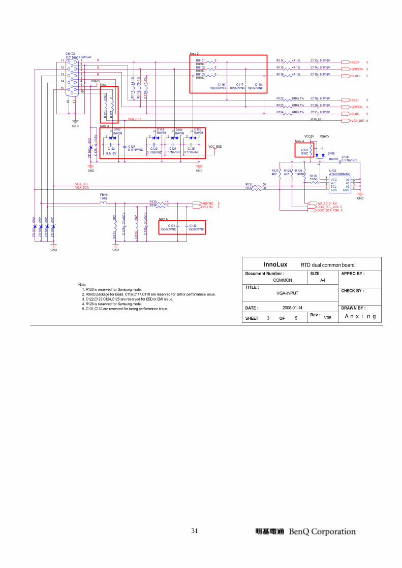
5.5 RGB CAPTURE
- Signal RED,GREEN,BLUE input through CN102 #1,#2,#3, Stop DC via R114&C113, R115&C114
and R116&C115 and then enter into U105 (scaler) analog input terminal #16,#14,#12, and then
scaler deals with signal internally.
- Signal DDC_SCL (series clock) inputs via CN102#15, and then passes through R131, goes into
U108#5.
- Signal DDC_SDA (series data) inputs via CN102#12, and then passes through R132, goes into
U108 #8.
- Signal TTL vertical sync. (Vsync) inputs via CN102 #14, and then clamped by ZD105 Zener,
passes through R134, and then goes into IC U105 (scaler) #8.
- Signal TTL horizontal sync. (Hsync) inputs via CN102 #13, and then clamped by ZD104 Zener,
passes through FB101,R133, and then goes into IC U105 (scaler) #9.
- CN102#5 is defined as cable detect pin, this detector realize passes through R184 Pull high, go
into U108#24.
5.5.1 Buttons Control
- Button “Power” in right of bezel connects to U108 #9 through R156, via CN104#8.
- Button “UP” “DOWN ““MENU” “ENTER” in the bottom of bezel connects to U108 #21,#22, through
R188,R189 via CN104 #2,#3
- U106 is an EEPROM IC which memory OSD setting and save the value adjusted by user.
- LED Indicator on Front Bezel
a. When press button “power”, U108#48 sends out a low potential, flow to CN104 #7 on keypad,
LED Green ON.
b. When in “Suspend” mode, U108 #1 sends out a low potential, flows to CN104 #5 on keypad,
LED Amber ON.
5.5.2 REALTEK CHIP U105 (scaler) &U108(MCU)
- U105 (RTD2035L) #29~#38 output 8 bit LVDS digital data to panel control circuit through CN105.
- U108 (RTD2122L ) #44 outputs Brightness “PWM” signals to control CCFL brightness.
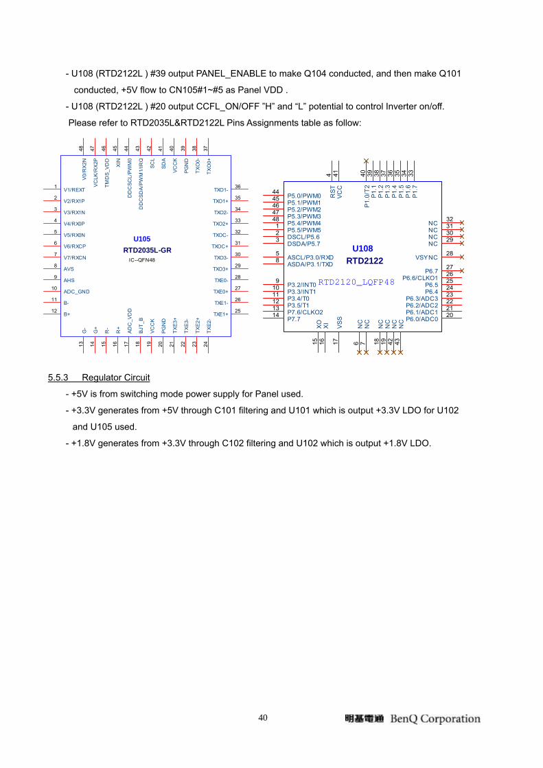
40
- U108 (RTD2122L ) #39 output PANEL_ENABLE to make Q104 conducted, and then make Q101
conducted, +5V flow to CN105#1~#5 as Panel VDD .
- U108 (RTD2122L ) #20 output CCFL_ON/OFF ”H” and “L” potential to control Inverter on/off.
Please refer to RTD2035L&RTD2122L Pins Assignments table as follow:
U105RTD2035L-GR
IC--QFN48
1
2
3
4
5
6
7
8
9
10
11
12
13 14 15 16 17 18 19 20 21 22 23 24
36
35
34
33
32
31
30
29
28
27
26
25
48 47 46 45 44 43 42 41 40 39 38 37
V1/REXT
V2/RX1P
V3/RX1N
V4/RX0P
V5/RX0N
V6/RXCP
V7/RXCN
AVS
AHS
ADC_GND
B-
B+
G-
G+
R-
R+
AD
C_V
DD
BJT
_B
VC
CK
PGN
D
TX
E3+
TX
E3-
TX
E2+
TX
E2-
TXO1-
TXO1+
TXO2-
TXO2+
TXOC-
TXOC+
TXO3-
TXO3+
TXE0-
TXE0+
TXE1-
TXE1+
V0/
RX
2N
VC
LK/R
X2P
TMD
S_V
DD
XIN
DD
CS
CL/
PW
M0
DD
CS
DA
/PW
M1/
IRQ
SC
L
SD
A
VCC
K
PGN
D
TX
O0-
TXO
0+
RTD2120_LQFP48
U108RTD2122
123
4
5
6 7
8
1715
41 40 39 38 37 36 35 34 33
19
28
29
2021222324252627
16
91011121314
18
303132
4342
4445464748
P5.5/PWM5DSCL/P5.6DSDA/P5.7
RS
T
ASCL/P3.0/RXD
NC
NC
ASDA/P3.1/TXD
VS
S
XO
VC
C
P1.
0/T
2P1
.1P1
.2P1
.3P1
.4P1
.5P1
.6P1
.7
NC
VSYNC
NC
P6.0/ADC0P6.1/ADC1P6.2/ADC2P6.3/ADC3
P6.4P6.5
P6.6/CLKO1P6.7
XI
P3.2/INT0P3.3/INT1P3.4/T0P3.5/T1P7.6/CLKO2P7.7
NC
NCNCNC
NC
NC
P5.0/PWM0P5.1/PWM1P5.2/PWM2P5.3/PWM3P5.4/PWM4
5.5.3 Regulator Circuit
- +5V is from switching mode power supply for Panel used.
- +3.3V generates from +5V through C101 filtering and U101 which is output +3.3V LDO for U102
and U105 used.
- +1.8V generates from +3.3V through C102 filtering and U102 which is output +1.8V LDO.
41
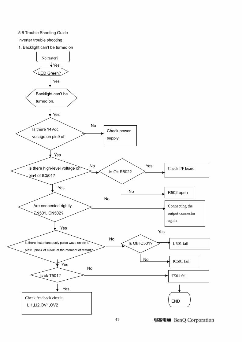
5.6 Trouble Shooting Guide
Inverter trouble shooting
1. Backlight can’t be turned on
No raster?
LED Green?
Yes
Yes
Yes
Backlight can’t be
turned on.
No Check power
supply
Is there high-level voltage on
pin4 of IC501?
No Is Ok R502?
Check I/F board Yes
R502 open NoYes
Is there instantaneously pulse wave on pin1,
pin11, pin14 of IC501 at the moment of restart?
No Is Ok IC501?
Yes
U501 fail
No IC501 fail
Yes
Is ok T501? T501 fail
Are connected rightly
CN501, CN502?
No
Connecting the
output connector
again
No
Check feedback circuit
LI1,LI2,OV1,OV2
Yes
END
Is there 14Vdc
voltage on pin9 of
Yes
Yes

42
Power trouble shooting_1
2. No Power & LED Off
No power
Check primary
rectifier voltage Check IC802,
C804, T801,
Check circuit if
short
Check F801, P801,
RT,801,D801
Check pin7 of IC802
voltage about 16V CheckC810,D803,C807,
Check pin2 of IC802 voltage
about 3V
Check primary OVP, OLP
and secondary
Check pin5 of IC802
voltage is below 1.4V
Check R804, R805
END

43
3. Unstable Power
Check sampling
Circuit
Check R811,
R818, R810,
R811, R818, R810,
Check the R pin
voltage of IC803
Check SCREW4*8 *2
Check D806 , C815 is shortCheck pin6 of IC802
voltage is 16V
Check pin1 of
IC802 voltage
Change IC803
Unstable power
ChangeD803
Change R803, R 807 R824, R825, R812
END
Check the C pin
voltage of

44
4. Black Screen
Black Screen
Power Fail Check power supply:
Pin1, 2 of CN101
Check Crystal of U108
Check CCFL - Enable
of U108
MCU Fail
Check: X101
Inverter Fail
OK
NG
OK
OK
NG
Check Reset
Of U108
Check pin5 of
CN101
Check R102,R103,
R106,Q103
Check RST Circuit
OK
NG
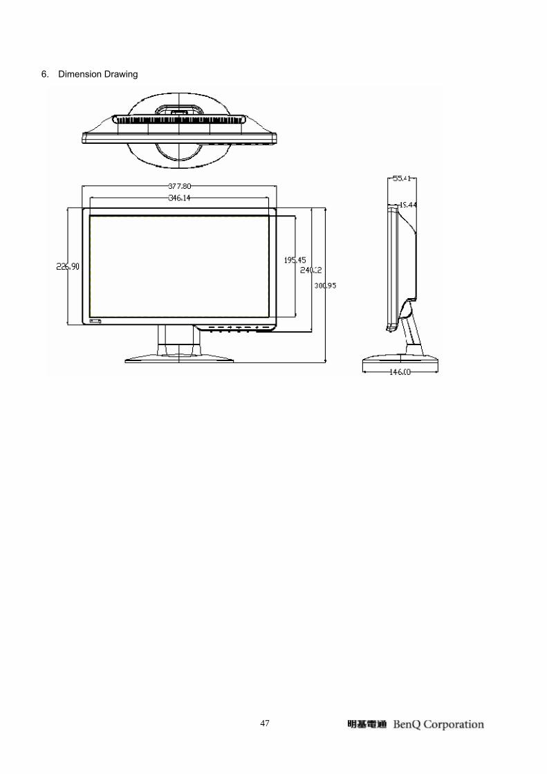
NG
NG
OK OK
Check power supply
supply of U108
NG
OK
Check U101,U102

45
5. White Screen
White Screen
LVDS Cable
Reinsert
Change LVDS
Cable
Check VLCD
Is 5V?
Check Panel - _Enable
Of U108 is High?
Check R107, R109, R110
Q101, Q104
END
Workmanship
LVDS Cable NG
Panel Fail Check LVDS
Signals
Check the HW Reset
Of U108
Check other pins
Of U108
Check RST Circuit
NG
NG
NG
NG
NG
NG
OK
OK
OK OK
OK

46
6. Bad Screen
Bad Screen
LVDS Cable
Reinsert
Change LVDS
Cable
Check the communication
of U105,U108 and external
circuit
Check the Pins of
The U105,U108
END
Workmanship
LVDS Cable NG
Check :MCU_SCLK,
Reset
NG
NG
NG
OK
OK
OK
Check Crystal Of U108
Check: X101
47
6. Dimension Drawing