Basic Memory Device Trends Toward the Vertical COPYRIGHTED ...
24
1 Basic Memory Device Trends Toward the Vertical 1.1 Overview of 3D Vertical Memory Book This book explores the current trend toward building electronic system chips in three dimensions (3D) and focuses on the memory part of these systems. This move to 3D is part of a long trend toward performance improvement and cost reduction of memories and memory system chips. Thirty years ago it was thought that if the chips could just be scaled and more transistors added every few years, the cost would continue to drop and the performance and capacity of the chips would continue to increase. The industry then struggled with the effect of scaling to small dimensions on the functionality and reliability of the memory technology. Along the way dynamic RAMs (DRAMs) replaced static RAMs (SRAMs) as the high-volume memory component. Twenty years ago the memory wall became the challenge. This gap in performance between DRAM memory technology and fast processor technology was solved by the clocked synchronous DRAM. Nonvolatile memories were developed. The quest for fast, high-density, nonvolatile memories became more urgent, so the NAND flash was invented, made synchro- nous, and became the mainstream memory component. Meanwhile the ability to integrate millions of transistors on scaled chips led to an increased effort to merge the memories and processors on the same chip. The many advantages of embedded memory on chip were explored and systems-on-chip became prevalent. Now systems-on-chip exhibit some of the same circuit issues that printed circuit boards with mounted chips in packages used to have. Redesigning these large, integrated chips into the third dimension should permit buses to be shortened and functions moved closer together to increase performance. System form factor can be reduced, and lower power consumption can permit smaller, lighter-weight batteries to be used in the handheld systems required today. This first chapter reviews these trends that have brought us to the point of moving into the third dimension. Chapter 2 focuses on vertical fin-shape field-effect transistors (FinFETs) used as flash memories both with silicon-on-insulator (SOI) and bulk substrates and on making stacked memories on multiple layers of single-crystal silicon. Chapter 3 discusses the advantages of gate-all-around nanowire nonvolatile memories, both with single-crystalline Vertical 3D Memory Technologies, First Edition. Betty Prince. © 2014 John Wiley & Sons, Ltd. Published 2014 by John Wiley & Sons, Ltd. COPYRIGHTED MATERIAL
Transcript of Basic Memory Device Trends Toward the Vertical COPYRIGHTED ...
1Basic Memory Device TrendsToward the Vertical
1.1 Overview of 3D Vertical Memory Book
This book explores the current trend toward building electronic system chips in threedimensions (3D) and focuses on the memory part of these systems. This move to 3D ispart of a long trend toward performance improvement and cost reduction of memories andmemory system chips.
Thirty years ago it was thought that if the chips could just be scaled and more transistorsadded every few years, the cost would continue to drop and the performance and capacity of thechips would continue to increase. The industry then struggled with the effect of scaling to smalldimensions on the functionality and reliability of the memory technology. Along the waydynamic RAMs (DRAMs) replaced static RAMs (SRAMs) as the high-volume memorycomponent. Twenty years ago the memory wall became the challenge. This gap in performancebetween DRAMmemory technology and fast processor technology was solved by the clockedsynchronous DRAM. Nonvolatile memories were developed. The quest for fast, high-density,nonvolatile memories became more urgent, so the NAND flash was invented, made synchro-nous, and became the mainstream memory component. Meanwhile the ability to integratemillions of transistors on scaled chips led to an increased effort to merge the memories andprocessors on the same chip. The many advantages of embedded memory on chip wereexplored and systems-on-chip became prevalent. Now systems-on-chip exhibit some of thesame circuit issues that printed circuit boards with mounted chips in packages used to have.Redesigning these large, integrated chips into the third dimension should permit buses to beshortened and functions moved closer together to increase performance. System form factorcan be reduced, and lower power consumption can permit smaller, lighter-weight batteries to beused in the handheld systems required today.
This first chapter reviews these trends that have brought us to the point of moving into thethird dimension. Chapter 2 focuses on vertical fin-shape field-effect transistors (FinFETs) usedas flash memories both with silicon-on-insulator (SOI) and bulk substrates and on makingstacked memories on multiple layers of single-crystal silicon. Chapter 3 discusses theadvantages of gate-all-around nanowire nonvolatile memories, both with single-crystalline
Vertical 3D Memory Technologies, First Edition. Betty Prince.© 2014 John Wiley & Sons, Ltd. Published 2014 by John Wiley & Sons, Ltd.
COPYRIG
HTED M
ATERIAL
substrate and with polysilicon core. Chapter 4 explores the vertical channel NAND flash withboth charge trapping and floating gate cells as well as stacked vertical gate NAND flash. Thesetechnologies promise high levels of nonvolatile memory integration in a small cube of silicon.Chapter 5 discusses the use of minimal-dimension memory cells in stacked, cross-point arraysusing the new resistive memory technologies. Chapter 6 focuses on the trend of stackedpackaging technology for DRAM systems using through-silicon-vias and microbumps tomigrate into a chip process technology resulting in high-density cubes of DRAM system chips.
1.2 Moore’s Law and Scaling
In the past 40 years electronics for data storage has moved from vacuum tubes to discretedevices to integrated circuits. It has moved from bipolar technology to complementary metal–oxide–silicon (CMOS), from standalone memories to embedded memories to embeddedsystems on chip. It is now poised to move into the third dimension. This move bringswith it opportunities and challenges. It opens a new and complex dimension in processtechnology and 3D design that only the computers, which have been a product of our journeythrough the development of electronics, can deal with along with their human handlers.
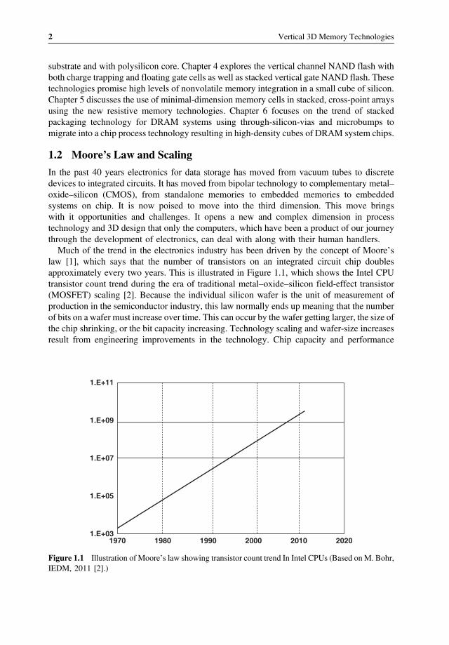
Much of the trend in the electronics industry has been driven by the concept of Moore’slaw [1], which says that the number of transistors on an integrated circuit chip doublesapproximately every two years. This is illustrated in Figure 1.1, which shows the Intel CPUtransistor count trend during the era of traditional metal–oxide–silicon field-effect transistor(MOSFET) scaling [2]. Because the individual silicon wafer is the unit of measurement ofproduction in the semiconductor industry, this law normally ends up meaning that the numberof bits on a wafer must increase over time. This can occur by the wafer getting larger, the size ofthe chip shrinking, or the bit capacity increasing. Technology scaling and wafer-size increasesresult from engineering improvements in the technology. Chip capacity and performance
1970 1980 1990 2000 2010 2020
1.E+11
1.E+09
1.E+07
1.E+05
1.E+03
Figure 1.1 Illustration of Moore’s law showing transistor count trend In Intel CPUs (Based on M. Bohr,IEDM, 2011 [2].)
2 Vertical 3D Memory Technologies
increases are driven by the demands of the application. These application demands are drivingthe move to 3D vertical memories.
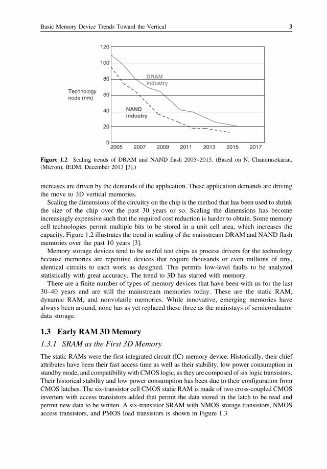
Scaling the dimensions of the circuitry on the chip is the method that has been used to shrinkthe size of the chip over the past 30 years or so. Scaling the dimensions has becomeincreasingly expensive such that the required cost reduction is harder to obtain. Some memorycell technologies permit multiple bits to be stored in a unit cell area, which increases thecapacity. Figure 1.2 illustrates the trend in scaling of the mainstream DRAM and NAND flashmemories over the past 10 years [3].
Memory storage devices tend to be useful test chips as process drivers for the technologybecause memories are repetitive devices that require thousands or even millions of tiny,identical circuits to each work as designed. This permits low-level faults to be analyzedstatistically with great accuracy. The trend to 3D has started with memory.
There are a finite number of types of memory devices that have been with us for the last30–40 years and are still the mainstream memories today. These are the static RAM,dynamic RAM, and nonvolatile memories. While innovative, emerging memories havealways been around, none has as yet replaced these three as the mainstays of semiconductordata storage.
1.3 Early RAM 3DMemory
1.3.1 SRAM as the First 3D Memory
The static RAMs were the first integrated circuit (IC) memory device. Historically, their chiefattributes have been their fast access time as well as their stability, low power consumption instandbymode, and compatibility with CMOS logic, as they are composed of six logic transistors.Their historical stability and low power consumption has been due to their configuration fromCMOS latches. The six-transistor cell CMOS static RAM is made of two cross-coupled CMOSinverters with access transistors added that permit the data stored in the latch to be read andpermit new data to be written. A six-transistor SRAM with NMOS storage transistors, NMOSaccess transistors, and PMOS load transistors is shown in Figure 1.3.
Technologynode (nm)
120
100
80
60
40
20
02005 2007 2009 2011 2013 2015 2017
DRAMindustry
NANDindustry
Figure 1.2 Scaling trends of DRAM and NAND flash 2005–2015. (Based on N. Chandrasekaran,(Micron), IEDM, December 2013 [3].)
Basic Memory Device Trends Toward the Vertical 3

The data is read from an SRAM starting with bit-line and bit-line high. The desired word-line is selected to open the access transistors, and the cell then pulls one of the bit-lines low. Thedifferential signal is detected on bit-line and bit-line, amplified by the sense amplifier, and readout through the output buffer. To write into the cell, data is placed on the bit-line and data on thebit-line, and then the word-line is activated. The cell is forced to flip into the state representedon the bit-lines, and the new state is stored in the flipflop.
One of the transistors in the CMOS inverters of an SRAM is always off, which hashistorically limited the static leakage path through the SRAM and given it both its stability andits very low standby power dissipation and retention capability at low voltage. The trendtoward lowering the power supply voltage in scaled SRAMs has reduced cell stability, usuallymeasured as static noise margin (SNM). It has also increased the subthreshold leakage and, as aresult, increased the static power dissipation. Thinner-scaled gate oxide increased the junctionleakage, while shorter channel length caused reduced gate control, resulting in short-channeleffects. Process variability made it more difficult for the matched transistors in the SRAM to beidentical so that the latch is turned off. An eight-transistor cell has been developed to improveread stability, but it increases the cell size [4].
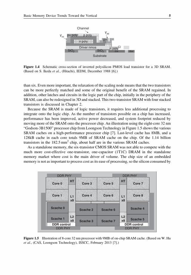
The development of double polysilicon technology in the late 1970s led to using one layer ofpolysilicon for load resistors to replace the PMOS load transistors in the six-transistor SRAM.These load resistors were stacked over the four NMOS transistors in the substrate [5]. Thismemory was fast, but it was difficult to tune the resistivity of the load resistors. In the late 1980sseveral companies used the new thin-film transistor (TFT) polysilicon technology to makestacked PMOS load transistors in the second layer of polysilicon [5]. These TFT PMOStransistors were stacked over the four NMOS transistors. These were the first 3D SRAMs. Aschematic cross-section of one of these polysilicon load transistor SRAMs is shown inFigure 1.4 [6]. This six-transistor SRAM cell used a bottom-gated polysilicon transistorstacked over NMOS transistors in the silicon substrate.
More recent efforts have been made to stack both the two PMOS load transistors and the twoNMOS pass transistors over the two pull-down NMOS transistors that remain in the siliconsubstrate. This allows the SRAM cell to occupy the space of two transistors on the chip rather
VDDVDD
VSSVSS
BL\BL
WLWL
Loadtransistors
Storage
transistors
Accesstransistor
Accesstransistor
Figure 1.3 Six-transistor SRAM with access, load, and storage transistors noted.
4 Vertical 3D Memory Technologies
than six. Even more important, the relaxation of the scaling node means that the two transistorscan be more perfectly matched and some of the original benefit of the SRAM regained. Inaddition, other latches and circuits in the logic part of the chip, initially in the periphery of theSRAM, can also be redesigned in 3D and stacked. This two-transistor SRAMwith four stackedtransistors is discussed in Chapter 2.
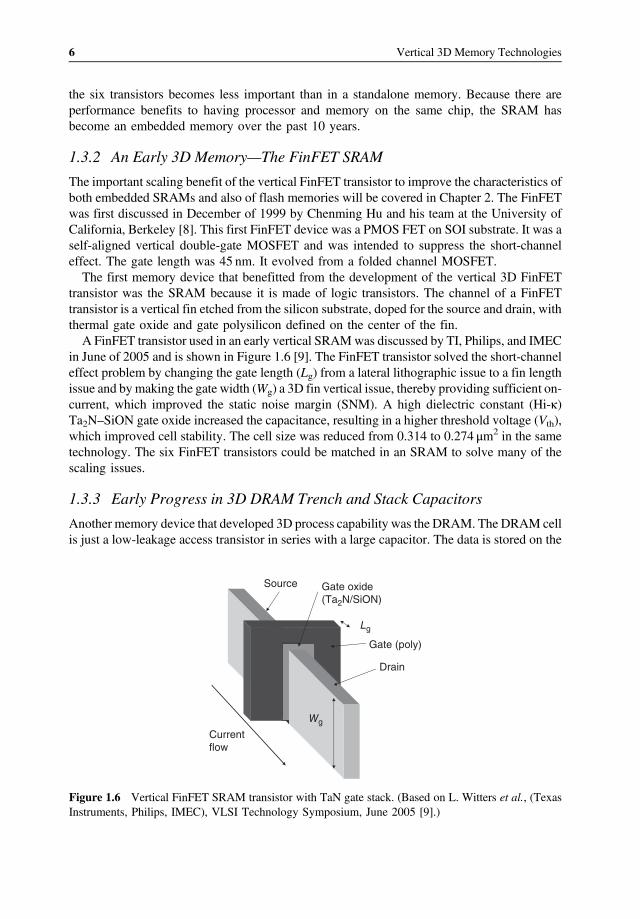
Because the SRAM is made of logic transistors, it requires less additional processing tointegrate onto the logic chip. As the number of transistors possible on a chip has increased,performance has been improved, active power decreased, and system footprint reduced bymoving more of the SRAM onto the processor chip. An illustration using the eight-core 32 nm“Godson-3B1500” processor chip from Loongson Technology in Figure 1.5 shows the variousSRAM caches on a high-performance processor chip [7]. Last-level cache has 8MB, and a128kB cache in each core totals 9MB of SRAM cache on the chip. Of the 1.14 billiontransistors in the 182.5mm2 chip, about half are in the various SRAM caches.
As a standalone memory, the six-transistor CMOS SRAM was not able to compete with themuch more cost-effective one-transistor, one-capacitor (1T1C) DRAM in the standalonememory market where cost is the main driver of volume. The chip size of an embeddedmemory is not as important to process cost as its ease of processing, so the silicon consumed by
Substrate
SiO2 SiO2n poly
n poly
n+ n+
p poly
Driver nmos
p+
Vccp+ poly
Channel
Vss
Figure 1.4 Schematic cross-section of inverted polysilicon PMOS load transistor for a 3D SRAM.(Based on S. Ikeda et al., (Hitachi), IEDM, December 1988 [6].)
Core 0
Core 1
Core 3
Core 4
Core 5
Core 6
Core 7
Core 8
Scache 0
Scache 1
Scache 4
Scache 5
Scache 2
Scache 3
Scache 6
Scache 7
L1
x8
L1
x8
L2
x8
L2
x8
HT HT
DDR control DDR controlDDR PHY DDR PHY
DDR PHY DDR PHY
Figure 1.5 Illustration of 8-core 32 nm processor with 9MB of on-chip SRAM cache. (Based on W. Huet al., (CAS, Loongson Technology), ISSCC, February 2013 [7].)
Basic Memory Device Trends Toward the Vertical 5
the six transistors becomes less important than in a standalone memory. Because there areperformance benefits to having processor and memory on the same chip, the SRAM hasbecome an embedded memory over the past 10 years.
1.3.2 An Early 3D Memory—The FinFET SRAM
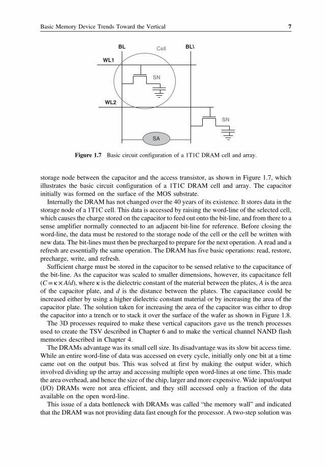
The important scaling benefit of the vertical FinFET transistor to improve the characteristics ofboth embedded SRAMs and also of flash memories will be covered in Chapter 2. The FinFETwas first discussed in December of 1999 by Chenming Hu and his team at the University ofCalifornia, Berkeley [8]. This first FinFET device was a PMOS FET on SOI substrate. It was aself-aligned vertical double-gate MOSFET and was intended to suppress the short-channeleffect. The gate length was 45 nm. It evolved from a folded channel MOSFET.
The first memory device that benefitted from the development of the vertical 3D FinFETtransistor was the SRAM because it is made of logic transistors. The channel of a FinFETtransistor is a vertical fin etched from the silicon substrate, doped for the source and drain, withthermal gate oxide and gate polysilicon defined on the center of the fin.
A FinFET transistor used in an early vertical SRAMwas discussed by TI, Philips, and IMECin June of 2005 and is shown in Figure 1.6 [9]. The FinFET transistor solved the short-channeleffect problem by changing the gate length (Lg) from a lateral lithographic issue to a fin lengthissue and bymaking the gate width (Wg) a 3D fin vertical issue, thereby providing sufficient on-current, which improved the static noise margin (SNM). A high dielectric constant (Hi-κ)Ta2N–SiON gate oxide increased the capacitance, resulting in a higher threshold voltage (Vth),which improved cell stability. The cell size was reduced from 0.314 to 0.274 μm2 in the sametechnology. The six FinFET transistors could be matched in an SRAM to solve many of thescaling issues.
1.3.3 Early Progress in 3D DRAM Trench and Stack Capacitors
Another memory device that developed 3D process capability was the DRAM. The DRAM cellis just a low-leakage access transistor in series with a large capacitor. The data is stored on the
Drain
Source
Lg
Currentflow
W
Gate (poly)
Gate oxide
(Ta2N/SiON)
Wg
Figure 1.6 Vertical FinFET SRAM transistor with TaN gate stack. (Based on L. Witters et al., (TexasInstruments, Philips, IMEC), VLSI Technology Symposium, June 2005 [9].)
6 Vertical 3D Memory Technologies
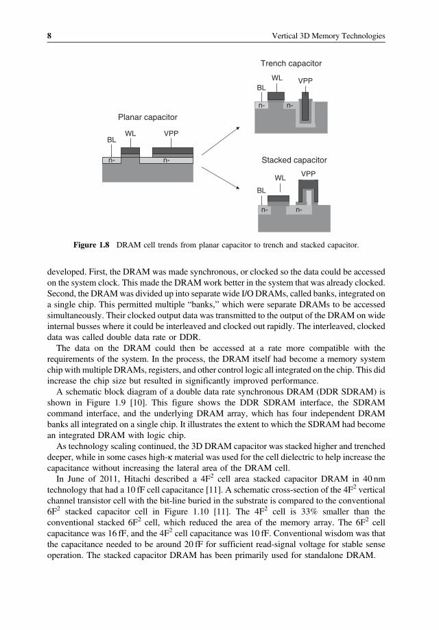
storage node between the capacitor and the access transistor, as shown in Figure 1.7, whichillustrates the basic circuit configuration of a 1T1C DRAM cell and array. The capacitorinitially was formed on the surface of the MOS substrate.
Internally the DRAM has not changed over the 40 years of its existence. It stores data in thestorage node of a 1T1C cell. This data is accessed by raising the word-line of the selected cell,which causes the charge stored on the capacitor to feed out onto the bit-line, and from there to asense amplifier normally connected to an adjacent bit-line for reference. Before closing theword-line, the data must be restored to the storage node of the cell or the cell be written withnew data. The bit-lines must then be precharged to prepare for the next operation. A read and arefresh are essentially the same operation. The DRAM has five basic operations: read, restore,precharge, write, and refresh.
Sufficient charge must be stored in the capacitor to be sensed relative to the capacitance ofthe bit-line. As the capacitor was scaled to smaller dimensions, however, its capacitance fell(C= κ×A/d), where κ is the dielectric constant of the material between the plates, A is the areaof the capacitor plate, and d is the distance between the plates. The capacitance could beincreased either by using a higher dielectric constant material or by increasing the area of thecapacitor plate. The solution taken for increasing the area of the capacitor was either to dropthe capacitor into a trench or to stack it over the surface of the wafer as shown in Figure 1.8.
The 3D processes required to make these vertical capacitors gave us the trench processesused to create the TSV described in Chapter 6 and to make the vertical channel NAND flashmemories described in Chapter 4.
The DRAMs advantage was its small cell size. Its disadvantage was its slow bit access time.While an entire word-line of data was accessed on every cycle, initially only one bit at a timecame out on the output bus. This was solved at first by making the output wider, whichinvolved dividing up the array and accessing multiple open word-lines at one time. This madethe area overhead, and hence the size of the chip, larger and more expensive. Wide input/output(I/O) DRAMs were not area efficient, and they still accessed only a fraction of the dataavailable on the open word-line.
This issue of a data bottleneck with DRAMs was called “the memory wall” and indicatedthat the DRAM was not providing data fast enough for the processor. A two-step solution was
WL1
BL
SN
WL2
BL\Cell
SN
SA
Figure 1.7 Basic circuit configuration of a 1T1C DRAM cell and array.
Basic Memory Device Trends Toward the Vertical 7
developed. First, the DRAM was made synchronous, or clocked so the data could be accessedon the system clock. This made the DRAMwork better in the system that was already clocked.Second, the DRAMwas divided up into separate wide I/O DRAMs, called banks, integrated ona single chip. This permitted multiple “banks,” which were separate DRAMs to be accessedsimultaneously. Their clocked output data was transmitted to the output of the DRAM on wideinternal busses where it could be interleaved and clocked out rapidly. The interleaved, clockeddata was called double data rate or DDR.
The data on the DRAM could then be accessed at a rate more compatible with therequirements of the system. In the process, the DRAM itself had become a memory systemchip with multiple DRAMs, registers, and other control logic all integrated on the chip. This didincrease the chip size but resulted in significantly improved performance.
A schematic block diagram of a double data rate synchronous DRAM (DDR SDRAM) isshown in Figure 1.9 [10]. This figure shows the DDR SDRAM interface, the SDRAMcommand interface, and the underlying DRAM array, which has four independent DRAMbanks all integrated on a single chip. It illustrates the extent to which the SDRAM had becomean integrated DRAM with logic chip.
As technology scaling continued, the 3D DRAM capacitor was stacked higher and trencheddeeper, while in some cases high-κmaterial was used for the cell dielectric to help increase thecapacitance without increasing the lateral area of the DRAM cell.
In June of 2011, Hitachi described a 4F2 cell area stacked capacitor DRAM in 40 nmtechnology that had a 10 fF cell capacitance [11]. A schematic cross-section of the 4F2 verticalchannel transistor cell with the bit-line buried in the substrate is compared to the conventional6F2 stacked capacitor cell in Figure 1.10 [11]. The 4F2 cell is 33% smaller than theconventional stacked 6F2 cell, which reduced the area of the memory array. The 6F2 cellcapacitance was 16 fF, and the 4F2 cell capacitance was 10 fF. Conventional wisdom was thatthe capacitance needed to be around 20 fF for sufficient read-signal voltage for stable senseoperation. The stacked capacitor DRAM has been primarily used for standalone DRAM.
n- n-
Planar capacitor
Trench capacitor
n- n-
Stacked capacitor
n- n-
BLVPPWL
BL
WL VPP
BL
WLVPP
Figure 1.8 DRAM cell trends from planar capacitor to trench and stacked capacitor.
8 Vertical 3D Memory Technologies

The trench capacitor DRAM continued to be developed for use in embedded memory. Aschematic cross-section and illustration of the 40:1 aspect ratio of the SOI 3D deep trenchDRAM cell used by IBM as Level 3 cache in its Power7TM Microprocessor was illustrated inJune of 2010 by IBM and is shown in Figure 1.11 [12].
In February of 2010, IBM described further the SOI deep trench capacitor 1Mb eDRAMmacro on this microprocessor [13]. A schematic block diagram of the Power7TM micro-processor in Figure 1.12 shows the SRAM L2 cache and DRAM L3 cache along with the eightcores and the memory controllers. The eDRAM cell size was 0.0672 μm2. The eDRAMmacro
SDRAM command interface DRAM array DDR SDRAM interface
Refresh counter
Clock generator CK
Command decode DLL
Control logicX16
X32 DriversMUXReadLatch
Row addressMUX
Moderegister
X16
DQSExtended
mode registerDQS
GeneratorData controllogic
X32Bankcontrol
Column address decoder
Addressregisters
WriteFIFO &drivers
X16X32 ReceiversInput
registerX16
CK
Bank 0 memory array
Columnaddress
Row addressLatch&decod
Figure 1.9 Schematic block diagram of basic double data rate (DDR) SDRAM. (Based on B. Prince,High Performance Memories, John Wiley & Sons, Ltd, 1999 [10].)
Figure 1.10 Stacked 3D DRAM cells in 40 nm technology (a) 6F2 16 fF conventional eDRAM cell; and(b) 4F2 10 fF vertical channel transistor pillar cell with buried bit-line. (Based on Y. Yanagawa et al.,(Hitachi), VLSI Circuits, June 2011 [11].)
Basic Memory Device Trends Toward the Vertical 9

was made in 45 nm fully depleted SOI technology. Thirty-two macros were used per coresupporting eight cores for a 32MB L3 on-chip cache in the 567mm2 microprocessor die. Thedeep trench had 25 times more capacitance than planar DRAM capacitor structures had, and itreduced on-chip voltage island supply noise. The 1Mb macro was made of four 292Ksubarrays that were organized 264 word-lines× 1200 bit-lines. There was a consolidated
BOX
pn
As n+
WLPassingWL
SiNocollar
Deeptrench
Nodenitride
Si substrate
n
Figure 1.11 Deep trench 3D capacitor DRAM used in microprocessor L3 cache. (Based on K. Agarwalet al., (IBM), VLSI Circuits Symposium, June 2010 [12].)
Core
L2 cache
Core Core Core
Core Core Core Core
L3 cache and chip interconnect Mem CtrlMem Ctrl
L2 cache L2 cache L2 cache
L2 cache L2 cache L2 cache L2 cache
Figure 1.12 Schematic block diagram of a microprocessor with embedded DRAM L3 cache. (Based onJ. Barth et al., (2011) (IBM), IEEE Journal of Solid-State Circuits, 46(1), 64 [14].)
10 Vertical 3D Memory Technologies
control logic and 146 I/Os where the inputs and outputs were pipelined. There were two rowaddress paths to permit concurrent refresh of a second subarray. Late selection was offered tosupport set associative cache designs. In order to have a high transfer ratio, an 18 fF deep trenchcell was used together with a 3.5 fF single-ended local bit-line. The DRAM macro used a1.05V power supply and had a 1.7 nm cycle time and a 1.35 nm access time.
In Chapter 6, a 3D two-chip TSV stacked system is explored, which includes a 45 nmeDRAM and logic blocks from this processor’s L3 cache [14].
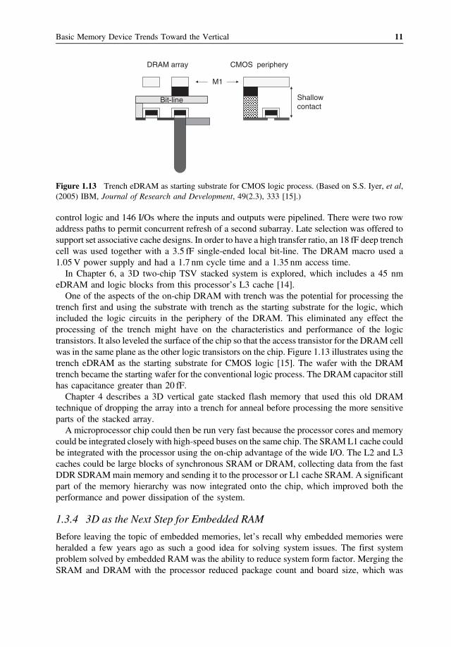
One of the aspects of the on-chip DRAM with trench was the potential for processing thetrench first and using the substrate with trench as the starting substrate for the logic, whichincluded the logic circuits in the periphery of the DRAM. This eliminated any effect theprocessing of the trench might have on the characteristics and performance of the logictransistors. It also leveled the surface of the chip so that the access transistor for the DRAM cellwas in the same plane as the other logic transistors on the chip. Figure 1.13 illustrates using thetrench eDRAM as the starting substrate for CMOS logic [15]. The wafer with the DRAMtrench became the starting wafer for the conventional logic process. The DRAM capacitor stillhas capacitance greater than 20 fF.
Chapter 4 describes a 3D vertical gate stacked flash memory that used this old DRAMtechnique of dropping the array into a trench for anneal before processing the more sensitiveparts of the stacked array.
A microprocessor chip could then be run very fast because the processor cores and memorycould be integrated closely with high-speed buses on the same chip. The SRAML1 cache couldbe integrated with the processor using the on-chip advantage of the wide I/O. The L2 and L3caches could be large blocks of synchronous SRAM or DRAM, collecting data from the fastDDR SDRAMmain memory and sending it to the processor or L1 cache SRAM. A significantpart of the memory hierarchy was now integrated onto the chip, which improved both theperformance and power dissipation of the system.
1.3.4 3D as the Next Step for Embedded RAM
Before leaving the topic of embedded memories, let’s recall why embedded memories wereheralded a few years ago as such a good idea for solving system issues. The first systemproblem solved by embedded RAM was the ability to reduce system form factor. Merging theSRAM and DRAM with the processor reduced package count and board size, which was
DRAM array CMOS periphery
Bit-line Shallowcontact
M1
Figure 1.13 Trench eDRAM as starting substrate for CMOS logic process. (Based on S.S. Iyer, et al,(2005) IBM, Journal of Research and Development, 49(2.3), 333 [15].)
Basic Memory Device Trends Toward the Vertical 11

critical in a world moving to portable handheld systems. I/O circuitry in the memory and logicchips, such as I/O buffers, bonding pads, and ESD circuitry, could be eliminated. Figure 1.14illustrates the reduction in system form factor made possible by embedding memory in logic.
Integrating the RAM with the processor also reduced active power consumption bypermitting wider on-chip buses, which could have the same bandwidth as off-chip busesbut with reduced speed because bandwidth equals bus speed times bus width. A lower powerconsumption meant the weight of the battery could be reduced and the life of the batteryextended. It also meant that the cost of cooling the high-speed processor could be reduced.
The integration of wide internal buses between RAM and processor on a single chip meantthat there were fewer external I/Os and wires, which reduced system electromagneticinterference (EMI). Additional I/O circuitry duplicated on separate chips in separate packageswas avoided, and ground bounce was reduced as was the need for custom bus and portconfigurations.
The ability to configure exactly the memory that is required on chip also eliminated siliconwasted on standard memory chip sizes. In addition, many logic chips were I/O limited. Becauseof the wide I/Os on the exterior of chips containing only a small amount of logic, the silicon wasnot used efficiently and the system footprint was increased by the large numbers of chips on theprinted circuit board. At the same time, the transistors were getting smaller and faster and moreof them could fit on each chip, so system chips became feasible. As a result, the system-on-chip(SoC) with processor and embedded memory increased in size and functionality and developedmany of the bus routing and interference issues that the system previously had. Resistive andcapacitive issues began to occur for long, thin on-chip busses. Some of the same issues thatdrove the integration of the SoC were now occurring on the system chip.
The next level of gaining back the advantages of integration of systems chips can come bymoving the circuits into 3D. Smaller-footprint system chips can be made, moving us back ontothe curve for Moore’s law. High-speed, wide, resistive-capacitive buses between processor and
Memory array
I/O buffersbonding pads
ESD
I/O buffersbonding pads
ESD
Logic
Memoryand logic
Figure 1.14 System form factor for (a) separate memory and logic chips; and (b) embedded memory inlogic chips.
12 Vertical 3D Memory Technologies
memory can, in 3D, again be shortened to reduce interference. Some of the advantages ofembedded memories can be regained at the current tighter geometries by using 3D effectively.
Chapter 6 explores the initial gains of through-silicon-vias (TSVs), which permit widememory buses to be connected locally in 3Dwith the appropriate logic circuit. The advantage ishigher-bandwidth buses and smaller footprints. The challenges are redesigning the circuits totake full advantage of the benefits of the move to the third dimension. Initially in 2.5Dtechnology, which uses interposers to redistribute the interconnects between standard chips,these vias are isolated on separate parts of the chip, where the large copper TSVs can’t interferetoo much with the sensitive logic and memory circuitry. As we learn more about using thesevias and see the gains of redesign for 3D, the interconnects could be more direct so theadvantages will multiply.
1.4 Early Nonvolatile Memories Evolve to 3D
1.4.1 NOR Flash Memory—Both Standalone and Embedded
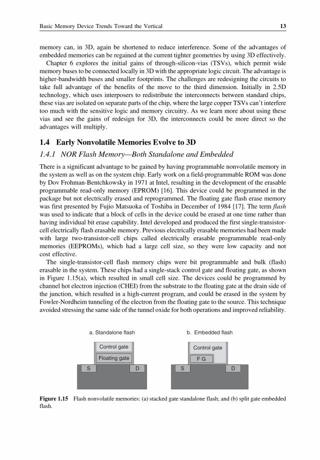
There is a significant advantage to be gained by having programmable nonvolatile memory inthe system as well as on the system chip. Early work on a field-programmable ROM was doneby Dov Frohman-Bentchkowsky in 1971 at Intel, resulting in the development of the erasableprogrammable read-only memory (EPROM) [16]. This device could be programmed in thepackage but not electrically erased and reprogrammed. The floating gate flash erase memorywas first presented by Fujio Matsuoka of Toshiba in December of 1984 [17]. The term flashwas used to indicate that a block of cells in the device could be erased at one time rather thanhaving individual bit erase capability. Intel developed and produced the first single-transistor-cell electrically flash erasable memory. Previous electrically erasable memories had been madewith large two-transistor-cell chips called electrically erasable programmable read-onlymemories (EEPROMs), which had a large cell size, so they were low capacity and notcost effective.
The single-transistor-cell flash memory chips were bit programmable and bulk (flash)erasable in the system. These chips had a single-stack control gate and floating gate, as shownin Figure 1.15(a), which resulted in small cell size. The devices could be programmed bychannel hot electron injection (CHEI) from the substrate to the floating gate at the drain side ofthe junction, which resulted in a high-current program, and could be erased in the system byFowler-Nordheim tunneling of the electron from the floating gate to the source. This techniqueavoided stressing the same side of the tunnel oxide for both operations and improved reliability.
b. Embedded flasha. Standalone flash
S D S D
Control gate
Floating gate
Control gate
F G
Figure 1.15 Flash nonvolatile memories: (a) stacked gate standalone flash; and (b) split gate embeddedflash.
Basic Memory Device Trends Toward the Vertical 13

Because the floating gate could be over-erased, leaving the channel in depletion mode so that itleaked when the gate was intended to be off, this device used an iterative erase procedure tocarefully define the voltage level of the erased state.
While the flash memory chips were initially made in volume production as standalonememory chips, there were advantages to integrating them onto the processor chip. For embeddedflash memory arrays, a split control gate cell was often used as shown in Figure 1.15(b). Thissplit control gate cell had a simplified erase because the control gate could turn the channel off,but the cell size was increased. This device used source-side CHEI from the substrate forprogramming, which used less current than the drain-side CHEI did in the standalone flashdevice. Erase was by poly-to-poly Fowler-Nordheim tunneling to the control gate, which was athick oxide process and therefore lower in cost to make and control.
A recent potential alternative for the NOR flash memory is the phase-change memory(PCM). This part is in low-volume production today. It works by heating a calcogenidematerial, causing a transition between a high-resistance state and a low-resistance state. Itsmain advantage over the NOR flash is in a faster transition between states. The PCM consumessignificant energy per bit and has issues with bit density [18]. It is unclear if this technology willtransition into a volume production memory or become another of the many alternativememory technologies that have appeared over the past 30 years but failed to replace the high-volume mainstream memory technologies.
1.4.2 The Charge-Trapping EEPROM
Nonvolatile MOS memories have also been around as long as SRAMs and DRAMs. The firstin-system, reprogrammable nonvolatile memories were called electrically alterable ROMs(EAROMs) or metal–nitride–oxide–silicon (MNOS) ROMs. MNOS reprogrammable ROMSwere reported as early as 1969 by Dov Frohman-Bentchkowsky when he was at FairchildSemiconductor [19].
P-channel MNOS EAROMs used silicon nitride (Si3N4) charge-trapping data storage, whichwas programmed and deprogrammed by Fowler-Nordheim tunneling through the tunnelingoxide (SiO2) between the substrate and the Si3N4, where the charges were trapped and stored.These low-capacity devices were used primarily in industrial and consumer circuits to storesmall amounts of data. They had a tunneling oxide and a nitride charge-trapping layer with analuminum gate. A schematic cross-section of an early MNOS cell is shown in Figure 1.16 [20].
Silicon substrate
p
Silicon dioxideSilicon nitride
Aluminum
p
DS
G
Figure 1.16 Schematic cross-section of an MNOS EAROM nonvolatile memory cell. (Based on B.Prince and G. Due-Gunderson, Semiconductor Memories, 1983, Figure 7.13, John Wiley & Sons,Ltd [20].)
14 Vertical 3D Memory Technologies
By 1989, MNOS charge-trapping EEPROMs with polysilicon gates, 28 nm Si2N4, and1.6 nm SiO2 were in volume production at Hitachi with yields equivalent to those of its SRAMlines [21]. In 1983, the Electrotechnical Laboratory in Japan suggested adding a blocking oxideto improve the reliability of the device, making the first MONOS electrically erasableprogrammable read-only memory (EEPROM) [22].
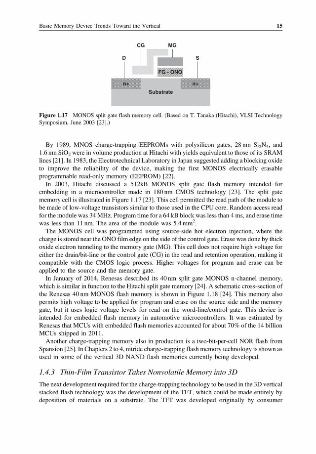
In 2003, Hitachi discussed a 512kB MONOS split gate flash memory intended forembedding in a microcontroller made in 180 nm CMOS technology [23]. The split gatememory cell is illustrated in Figure 1.17 [23]. This cell permitted the read path of the module tobe made of low-voltage transistors similar to those used in the CPU core. Random access readfor the module was 34 MHz. Program time for a 64 kB block was less than 4 ms, and erase timewas less than 11 nm. The area of the module was 5.4mm2.
The MONOS cell was programmed using source-side hot electron injection, where thecharge is stored near the ONO film edge on the side of the control gate. Erase was done by thickoxide electron tunneling to the memory gate (MG). This cell does not require high voltage foreither the drain/bit-line or the control gate (CG) in the read and retention operation, making itcompatible with the CMOS logic process. Higher voltages for program and erase can beapplied to the source and the memory gate.
In January of 2014, Renesas described its 40 nm split gate MONOS n-channel memory,which is similar in function to the Hitachi split gate memory [24]. A schematic cross-section ofthe Renesas 40 nm MONOS flash memory is shown in Figure 1.18 [24]. This memory alsopermits high voltage to be applied for program and erase on the source side and the memorygate, but it uses logic voltage levels for read on the word-line/control gate. This device isintended for embedded flash memory in automotive microcontrollers. It was estimated byRenesas that MCUs with embedded flash memories accounted for about 70% of the 14 billionMCUs shipped in 2011.
Another charge-trapping memory also in production is a two-bit-per-cell NOR flash fromSpansion [25]. In Chapters 2 to 4, nitride charge-trapping flash memory technology is shown asused in some of the vertical 3D NAND flash memories currently being developed.
1.4.3 Thin-Film Transistor Takes Nonvolatile Memory into 3D
The next development required for the charge-trapping technology to be used in the 3D verticalstacked flash technology was the development of the TFT, which could be made entirely bydeposition of materials on a substrate. The TFT was developed originally by consumer
Substrate
n+
FG - ONO
D S
n+
MGCG
Figure 1.17 MONOS split gate flash memory cell. (Based on T. Tanaka (Hitachi), VLSI TechnologySymposium, June 2003 [23].)
Basic Memory Device Trends Toward the Vertical 15
companies for use in the circuitry made on glass around the outside of flat panel displays.Development of cost-effective 3D stacked layers of silicon circuits depended on this advance.
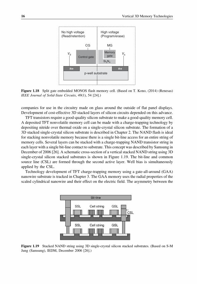
TFT transistors require a good-quality silicon substrate to make a good-quality memory cell.A deposited TFT nonvolatile memory cell can be made with a charge-trapping technology bydepositing nitride over thermal oxide on a single-crystal silicon substrate. The formation of a3D stacked single-crystal silicon substrate is described in Chapter 2. The NAND flash is idealfor stacking nonvolatile memory because there is a single bit-line access for an entire string ofmemory cells. Several layers can be stacked with a charge-trapping NAND transistor string ineach layer with a single bit-line contact to substrate. This concept was described by Samsung inDecember of 2006 [26]. A schematic cross-section of a vertical stacked NAND string using 3Dsingle-crystal silicon stacked substrates is shown in Figure 1.19. The bit-line and commonsource line (CSL) are formed through the second active layer. Well bias is simultaneouslyapplied by the CSL.
Technology development of TFT charge-trapping memory using a gate-all-around (GAA)nanowire substrate is tracked in Chapter 3. The GAA memory uses the radial properties of thescaled cylindrical nanowire and their effect on the electric field. The asymmetry between the
n+ n+
Control gate
Si3N4
Memory
gate
No high voltage
(Read/retention)
High voltage(Program/erase)
Vd Vs
CG MG
p-well substrate
Figure 1.18 Split gate embedded MONOS flash memory cell. (Based on T. Kono, (2014) (Renesas)IEEE Journal of Solid-State Circuits, 49(1), 54 [24].)
Figure 1.19 Stacked NAND string using 3D single-crystal silicon stacked substrates. (Based on S-MJung (Samsung), IEDM, December 2006 [26].)
16 Vertical 3D Memory Technologies
electric field of the tunneling oxide and that of the blocking oxide due to the radial design of theGAA meant that a fair-quality charge trapping transistor could be made with a polysiliconsubstrate. It was also discovered that shrinking the size of the GAAmemory meant that the sizeof the polysilicon grains was similar to the size of the channel; the channel was effectivelysingle-crystal silicon without grain boundaries to be crossed. These GAA memory devices areexplored in Chapters 3 and 4.
1.4.4 3D Microcontroller Stacks with Embedded SRAM and EEPROM
Microcontrollers are ubiquitous today. By 2015, 20 billion U.S. dollars worth of MCU areexpected to be shipped worldwide. All of them have RAMmemory, andmany have nonvolatilememory, EEPROM, or flash memory, which is named for its property of having a bulk, orflash, erase. These devices have multiple buses between MCU and memory cores includingflash memory and SRAM.
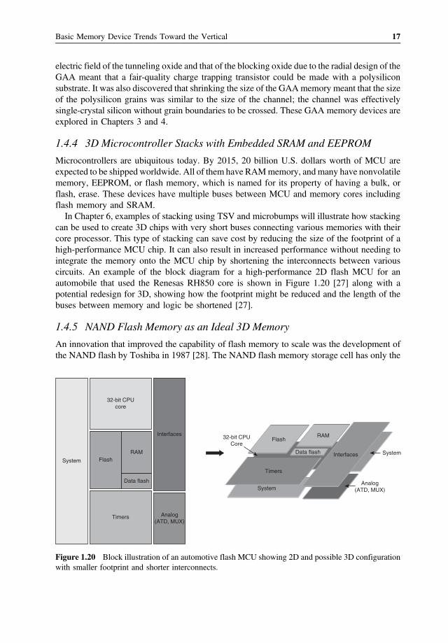
In Chapter 6, examples of stacking using TSV and microbumps will illustrate how stackingcan be used to create 3D chips with very short buses connecting various memories with theircore processor. This type of stacking can save cost by reducing the size of the footprint of ahigh-performance MCU chip. It can also result in increased performance without needing tointegrate the memory onto the MCU chip by shortening the interconnects between variouscircuits. An example of the block diagram for a high-performance 2D flash MCU for anautomobile that used the Renesas RH850 core is shown in Figure 1.20 [27] along with apotential redesign for 3D, showing how the footprint might be reduced and the length of thebuses between memory and logic be shortened [27].
1.4.5 NAND Flash Memory as an Ideal 3D Memory
An innovation that improved the capability of flash memory to scale was the development ofthe NAND flash by Toshiba in 1987 [28]. The NAND flash memory storage cell has only the
32-bit CPUcore
Timers Analog(ATD, MUX)
Interfaces
FlashRAM
Data flash
System
32-bit CPUCore
FlashRAM
Data flash System
SystemAnalog
(ATD, MUX)
Timers
Interfaces
Figure 1.20 Block illustration of an automotive flash MCU showing 2D and possible 3D configurationwith smaller footprint and shorter interconnects.
Basic Memory Device Trends Toward the Vertical 17
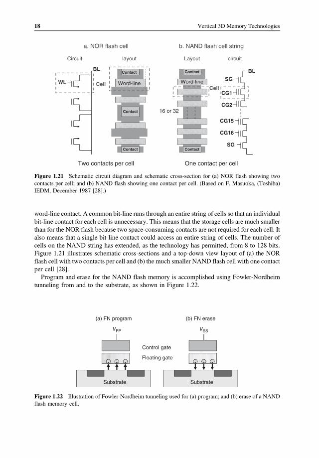
word-line contact. A common bit-line runs through an entire string of cells so that an individualbit-line contact for each cell is unnecessary. This means that the storage cells are much smallerthan for the NOR flash because two space-consuming contacts are not required for each cell. Italso means that a single bit-line contact could access an entire string of cells. The number ofcells on the NAND string has extended, as the technology has permitted, from 8 to 128 bits.Figure 1.21 illustrates schematic cross-sections and a top-down view layout of (a) the NORflash cell with two contacts per cell and (b) the much smaller NAND flash cell with one contactper cell [28].
Program and erase for the NAND flash memory is accomplished using Fowler-Nordheimtunneling from and to the substrate, as shown in Figure 1.22.
a. NOR flash cell b. NAND flash cell string
Circuit layout circuitLayout
One contact per cellTwo contacts per cell
Contact
Contact
Contact
CellCell
Word-line Word-line
Contact
Contact
BL
16 or 32
BL
SG
SG
CG1
CG2
CG15
CG16
WL
Figure 1.21 Schematic circuit diagram and schematic cross-section for (a) NOR flash showing twocontacts per cell; and (b) NAND flash showing one contact per cell. (Based on F. Masuoka, (Toshiba)IEDM, December 1987 [28].)
(a) FN program (b) FN erase
Substrate
- - -
VPP
Substrate
- - -
VSS
Control gate
Floating gate
Figure 1.22 Illustration of Fowler-Nordheim tunneling used for (a) program; and (b) erase of a NANDflash memory cell.
18 Vertical 3D Memory Technologies
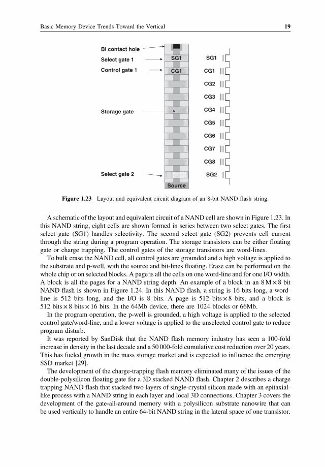
A schematic of the layout and equivalent circuit of a NAND cell are shown in Figure 1.23. Inthis NAND string, eight cells are shown formed in series between two select gates. The firstselect gate (SG1) handles selectivity. The second select gate (SG2) prevents cell currentthrough the string during a program operation. The storage transistors can be either floatinggate or charge trapping. The control gates of the storage transistors are word-lines.
To bulk erase the NAND cell, all control gates are grounded and a high voltage is applied tothe substrate and p-well, with the source and bit-lines floating. Erase can be performed on thewhole chip or on selected blocks. A page is all the cells on one word-line and for one I/O width.A block is all the pages for a NAND string depth. An example of a block in an 8M× 8 bitNAND flash is shown in Figure 1.24. In this NAND flash, a string is 16 bits long, a word-line is 512 bits long, and the I/O is 8 bits. A page is 512 bits× 8 bits, and a block is512 bits× 8 bits× 16 bits. In the 64Mb device, there are 1024 blocks or 66Mb.
In the program operation, the p-well is grounded, a high voltage is applied to the selectedcontrol gate/word-line, and a lower voltage is applied to the unselected control gate to reduceprogram disturb.
It was reported by SanDisk that the NAND flash memory industry has seen a 100-foldincrease in density in the last decade and a 50 000-fold cumulative cost reduction over 20 years.This has fueled growth in the mass storage market and is expected to influence the emergingSSD market [29].
The development of the charge-trapping flash memory eliminated many of the issues of thedouble-polysilicon floating gate for a 3D stacked NAND flash. Chapter 2 describes a chargetrapping NAND flash that stacked two layers of single-crystal silicon made with an epitaxial-like process with a NAND string in each layer and local 3D connections. Chapter 3 covers thedevelopment of the gate-all-around memory with a polysilicon substrate nanowire that canbe used vertically to handle an entire 64-bit NAND string in the lateral space of one transistor.
SG1
CG1
CG5
CG4
CG3
CG2
CG8
SG2
CG6
CG7
SG1
Source
CG1
Bl contact hole
Select gate 1
Control gate 1
Storage gate
Select gate 2
Figure 1.23 Layout and equivalent circuit diagram of an 8-bit NAND flash string.
Basic Memory Device Trends Toward the Vertical 19

In Chapter 4, both the vertical channel and the vertical gate NAND flash string are explored forlarge vertical arrays that are expected to produce terrabit NAND flash memory.
1.5 3D Cross-Point Arrays with Resistance RAM
Cross-point arrays, also called crossbar arrays, have seen significant research effort in the pastfew years. These 3D arrays have the attribute of being inherently stackable and composed ofvery compact 4–6F2 memory cells. The final vision of the large-scale 3D memory is astackable, addressable array of 4F2 memory cells with minimal peripheral area for memorymanagement. Any two-terminal resistance change memory can be used in a cross-point array.These memories are normally referred to as resistance RAMs (ReRAM). Several ReRAMtypes are discussed in the context of forming cross-point memory arrays in Chapter 5. Aschematic top view of a cross-point array indicating the 4F2 cell is shown in Figure 1.25.
Metal–oxide ReRAMs began to be widely reported in about 2004. They show promiseconfigured in a 3D cross-point array architecture. These ReRAMs have been studied in variousmaterials that will be discussed in Chapter 5 along with the cross-point array architecture. AReRAM can be configured as either a bipolar or a unipolar operating memory device. If itswitches by reversing the polarity of the applied voltage, then it is considered bipolar, and if itswitches using only different voltage pulses applied in a single direction, then it is consideredunipolar. The filamentary ReRAM has a low power per bit. The cell is stochastic and difficult tocontrol because only a few atoms are involved in the distribution [3].
The PCM has also been described in a cross-point array configuration. This resistance-typememory device works by joule heating of a chalcogenide material followed by differentcooling rates that determine whether the material ends up in a crystalline, low-resistance stateor an amorphous, high-resistance state.
Chapter 5 is devoted to the 3D cross-point array memory technology and the ReRAMs andselector devices used in them. Characteristics of two-terminal memory devices that could usethe cross-point array configuration are nonlinearity and bipolar or unipolar switching.
One block = 16 pages= 528 bytes x 16
1 page = 528 bytes
512 bits (word-line)
8 bit I/O
1 device = 1024 blocks
Figure 1.24 8M× 8 NAND flash memory array organization.
20 Vertical 3D Memory Technologies

1.6 STT-MTJ Resistance Switches in 3D
A spin-RAM that is programmed by interaction of a spin-transfer torque (STT) current and themagnetic moment of the magnetic layers in a magnetic tunnel junction (MTJ) was firstdescribed by Sony in December of 2005 [30]. An external magnetic field was not necessary toswitch the state of the device, differentiating it from the earlier field-programmable MRAMs. A4Kb spin-RAMwas made on a four-level, metal 180 nm CMOS process. Write speed was 2 ns,and write current was 200 μA. The spin-torque programming reduced the write current to about5% of the power required to write a field-programmable MTJ MRAM device. Workingprototypes were expected in a few years. The theory of the STT-RAMwas that the direction ofthe free magnetic layer in anMTJ device could be reversed by direct injection of spin-polarizedelectrons. Figure 1.26 illustrates STT switching in an MTJ [30].
2.0F
BL-3BL-2BL-1
WL-1
WL-2
WL-3
4F2 cell
2.0F
Figure 1.25 Schematic top view of a 4F2 cross-point memory array.
F2F1
e–
M1M2
dM1/dtdM2/dt
MgO
Figure 1.26 Illustration of spin-transfer torque switching in an MTJ. (Based on M. Hosomi et al.,(Sony), IEDM, December 2005 [30].)
Basic Memory Device Trends Toward the Vertical 21

The MTJ is made of a pinned layer (F1), an MgO tunnel barrier layer, and a free magneticlayer (F2). The mechanism used to switch the states is the spin of an electron, which has twostates: “up” or “down.” As a result, this memory is often referred to as a spintronics device.When a spin-polarized electron flows from F2 to F1, the spin direction is rotated by thedirection of the magnetic moments of the twomagnetic layers. The rotating of the spin directionof the electrons creates a spin torque, dM1/dt and dM2/dt, which acts on the magnetic momentofM1 andM2. When the torque is sufficiently large, the magnetization of the free layer F2 (M2)is reversed. This changes the magnetization of F1 and F2 from parallel to antiparallel, whichreduces the amount of current that can flow through theMTJ. If the electron current flows in theother direction through the MTJ, the spin of the electrons can reverse the state from antiparallelto parallel so that more current flows through the MTJ. The STT-MTJ memory is, therefore, aresistance change memory that uses the direction of current flow through the device to switchthe memory state between a high-resistance state (HRS) and a low-resistance state (LRS).
A current that flows from the free magnetic layer to the fixed magnetic layer can change thestate of the MTJ element from antiparallel to parallel (write “1”). A current that flows from thefixed magnetic layer to the free magnetic layer can change the state of the MTJ element fromparallel to antiparallel (write “0”), as shown in Figure 1.27 [31]. A few STT-MTJ researchdevices are discussed in Chapter 5 in cross-point array configurations and in Chapter 6 instacked TSV chips.
1.7 The Role of Emerging Memories in 3D Vertical Memories
In the process of developing new generations of memory technologies, a number of attemptshave been made to develop more scalable memory devices than the SRAM, DRAM, andflash memories. These conventional memory types have been around for more than 30 years,essentially without change in basic function. For the most part, the “emerging memories”have not yet made it into volume production despite significant amounts of developmenteffort. It appears to date that it has been safer to continue developing and scaling the threehistorical memories than to invest huge amounts on a gamble on new and untriedtechnologies. In this category are the ferroelectric RAM, the field-programmable magnetic
Figure 1.27 STT MTJ MRAM programming illustration of writing “1” and writing “0.” (Based on F.Tabrizi, EE Times, April 2007 [31].)
22 Vertical 3D Memory Technologies

RAM, various single-transistor memories, the negative resistance RAM, the nanotube RAM,and so on [18]. Some of these emerging memories have moved into small-scale production,primarily at startup companies, while others have effectively vanished. The ovonic memory,later called the phase-change memory, has entered low-volume production at several largecompanies and has also been discussed in a few development papers for cross-point arrays.
The ReRAM, even though a relatively new device, appears to have potential for use in thecross-point arrays and is discussed in this 3D variation in Chapter 5. These ReRAM devicesbegan to be described in about 2003 and are still being studied in a variety of different materialtechnologies. A description of various ReRAMs in cross-point arrays is given in Chapter 5.These cross-point array resistive memory devices are in early development and may takesignificant effort to develop into a mainstream memory technology.
The STT-MTJ memory is also a fairly recent memory device that has been described invarious 3D configurations such as a folded gate memory in Chapter 2, in cross-point arrays inChapter 5, and in stacked TSV chips in Chapter 6. It is still in early development and isexpected to take significant effort to develop into a mainstream memory technology.
There is little indication at this time that any of the emerging memory devices will replace thehistorical SRAM, DRAM, and flash in volume production in 3D memories in the near future.
References
1. Moore, G. (1965) Cramming more components onto integrated circuits. Electronics, 38(8), 114.2. Bohr, M. (December 2011) The evolution of scaling from the homogeneous era to the heterogeneous era. IEDM.3. Chandrasekaran,N.(December2013)Challenges in3Dmemorymanufacturingandprocess integration(Micron). IEDM.4. Chang, L. et al. (June 2005) Stable SRAM cell design for the 32 nm node and beyond, (IBM). VLSI Technology
Symposium.5. Prince, B. (1995) Semiconductor Memories: A Handbook of Design, Manufacture, and Application, 2nd edn, John
Wiley & Sons, Ltd.6. Ikeda, S. et al. (December 1988) A polysilicon transistor technology for large capacity SRAMs, (Hitachi). IEDM.7. Hu, W. et al. (February 2013) Godson-3B1500: A 32 nm 1.35GHz 40W 172.8 GFLOPS 8-core processor,
(Chinese Academy of Science, Loongson Technology). ISSCC.8. Huang, X. et al. (December 1999) Sub 50-nm FinFET: PMOS, (University of California, Berkeley, Lawrence
Berkeley National Laboratory). IEDM, p. 67.9. Witters, L. et al. (June 2005) Integration of tall triple-gate devices with inserted-TaxNy gate in a 0.274 μm2 6T-
SRAM cell and advanced CMOS logic circuits, (Texas Instruments, Philips, IMEC). VLSI TechnologySymposium.
10. Prince, B. (1999) High Performance Memories, John Wiley & Sons, Ltd, Figure 6.45, p. 186.11. Yanagawa, Y., Sekiguchi, T., Kotabe, A. et al. (June 2011) In-substrate-bitline sense amplifier with array-noise-
gating scheme for low-noise 4F2 DRAM array operable at 10 fF cell capacitance, (Hitachi). VLSI CircuitsSymposium.
12. Agarwal, K., Hayes, J., Berth, J. et al. (June 2010) In-situ measurement of variability in 45-nm SOI embeddedDRAM arrays, (IBM). VLSI Circuits Symposium.
13. Barth, J. et al. (February 2010) A 45 nm SOI embedded DRAM macro for POWER7TM 32MB on-chip L3 cache,(IBM). ISSCC.
14. Barth, J. et al. (2011) A 45 nm SOI embedded DRAMmacro for the POWER7TM processor 32MByte on-chip L3cache, (IBM). IEEE Journal of Solid-State Circuits, 46(1), 64.
15. Iyer, S.S. et al. (2005) Embedded DRAM: Technology platform for the Blue Gene/L chip. IBM Journal ofResearch and Development, 49(2.3), 333.
16. Frohman-Bentchkowsky, D. (1971) Memory behavior in a floating-gate avalanche -injection MOS (FAMOS)structure, (Intel). Applied Physics Letters, 18(8), 332.
17. Masuoka, F., Asano, M., Iwahashi, H. et al. (December 1984) A new flash E2PROM cell using triple polysilicontechnology, (Toshiba). IEDM.
Basic Memory Device Trends Toward the Vertical 23
18. Prince, B. (2002) Emerging Memories Technologies and Trends, Kluver Academic Publishers.19. Frohman-Bentchkowsky, D. (1969) An integrated metal-nitride-oxide-silicon (MNOS) memory, (Fairchild
Semiconductor). Proceedings of the IEEE, 57(6), 1190.20. Prince, B. and Due-Gunderson, G. (1983) Semiconductor Memories, John Wiley & Sons, Ltd.21. Kamigaki, Y. et al. (1989) Yield and reliability of MNOS EEPROM products, (Hitachi). IEEE Journal of Solid-
State Circuits, 24(6), 1714.22. Suzuki, E., Hiraishi, H., Ishii, Kenichi, and Hayashi, Y. (1983) A low-voltage alterable EEPROM with metal-
oxide-nitride-oxide-semiconductor (MONOS) structures, (Electrotechnical Laboratory Ibaraki Japan, CitizenWatch Co.). IEEE Transactions on Education, ED-30(2), 122.
23. Tanaka, T., Tanikawa, H., Yamaki, T., and Umeboto, Y. (June 2003) A 512kB MONOS type flash memorymodule embedded in a microcontroller, (Hitachi). VLSI Technology Symposium.
24. Kono, T. et al. (2014) 40-nm embedded split-gate MONOS (SG-MONOS) flash macros for automotive with160-MHz random access for code and endurance over 10 M cycles for data at the junction temperature of170 °C, (Renesas). IEEE Journal of Solid-State Circuits, 49(1), 154.
25. Spansion (2009) Spansion Launches MirrorBit(R) SPI Multi-I/O Flash Memory with Up to 40 MB/s ReadPerformance. Press release, May 20.
26. Jung, S.-M. (December 2006) Three dimensionally stacked NAND flash memory technology using stacking singlecrystal Si layers on ILD and TANOS structure for beyond 30 nm node, (Samsung). IEDM.
27. Renesas (2014) RH850 Family (Automotive Only), http://www.renesas.com/products/mpumcu/rh850 (accessed14 May 2014).
28. Masuoka, F., Momodomi, M., Iwata, Y., and Shirota, R. (December 1987) New ultra high density EPROM andflash EEPORM with NAND structure cell, (Toshiba). IEDM.
29. Quader, K.N. (20 May 2012) Flash memory at a cross-road: Challenges & opportunities, (SanDisk). IMW.30. Hosomi, M. et al. (December 2005) A novel nonvolatile memory with spin torque transfer magnetization
switching: Spin RAM, (Sony). IEDM.31. Tabrizi, F. (2007) Taking Hold of Embedded Memory Management, (Grandis). EE Times (April 23).
24 Vertical 3D Memory Technologies


![COPYRIGHTED MATERIAL · 2020. 2. 2. · ends, and toward spurious rationalism. His works include Minima moralia (1974 [German 1951]), Prisms (1967 [German 1955]), and Negative dialectics](https://static.fdocuments.in/doc/165x107/6132546bdfd10f4dd73a6118/copyrighted-material-2020-2-2-ends-and-toward-spurious-rationalism-his-works.jpg)