Basic Materials Science for MEMS Fundamentals of …gale/mems/Lecture 06 Materials... ·...
12
Fundamentals of Micromachining Dr. Bruce K. Gale BIOEN 6421 EL EN 5221 and 6221 ME EN 5960 and 6960 Basic Materials Science for MEMS • Basic material interactions • Silicon as a material • Crystallography • Crystal defects and impurities • Wafer manufacture • Stress and strain • Review of class projects Sensors and Actuators • “Sensor” (Latin sentire meaning “to perceive”) • “Transducer” (Latin transducere meaning “to lead across”) • A sensor performs a transducing action and the transducers must necessarily sense some physical or chemical signals • Types of signals: chemical, electrical, magnetic, mechanical, radiant, thermal Materials Overview • Metals – Characterized by metallic bonds • Polymers – Long chain molecules of repeating units • Ceramics – Inorganic compounds with ionic and covalent bonding • Others- glass (non-crystalline solids) and carbon
Transcript of Basic Materials Science for MEMS Fundamentals of …gale/mems/Lecture 06 Materials... ·...

Fundamentals of Micromachining
Dr. Bruce K. GaleBIOEN 6421
EL EN 5221 and 6221ME EN 5960 and 6960
Basic Materials Science for MEMS• Basic material interactions• Silicon as a material• Crystallography• Crystal defects and impurities• Wafer manufacture• Stress and strain• Review of class projects
Sensors and Actuators• “Sensor” (Latin sentire meaning “to perceive”)• “Transducer” (Latin transducere meaning “to
lead across”)• A sensor performs a transducing action and the
transducers must necessarily sense some physical or chemical signals
• Types of signals: chemical, electrical, magnetic, mechanical, radiant, thermal
Materials Overview• Metals
– Characterized by metallic bonds• Polymers
– Long chain molecules of repeating units• Ceramics
– Inorganic compounds with ionic and covalent bonding
• Others- glass (non-crystalline solids) and carbon
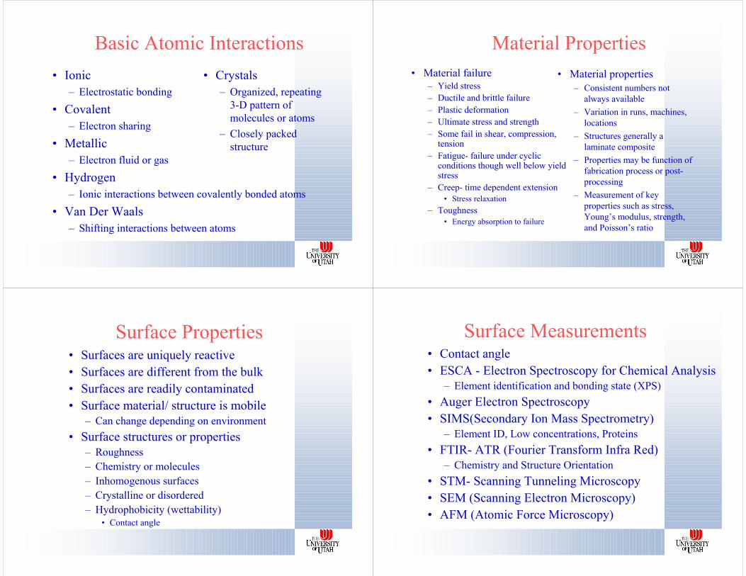
Basic Atomic Interactions• Ionic
– Electrostatic bonding
• Covalent– Electron sharing
• Metallic– Electron fluid or gas
• Hydrogen– Ionic interactions between covalently bonded atoms
• Van Der Waals– Shifting interactions between atoms
• Crystals– Organized, repeating
3-D pattern of molecules or atoms
– Closely packed structure
Material Properties• Material failure
– Yield stress– Ductile and brittle failure– Plastic deformation– Ultimate stress and strength– Some fail in shear, compression,
tension– Fatigue- failure under cyclic
conditions though well below yield stress
– Creep- time dependent extension• Stress relaxation
– Toughness• Energy absorption to failure
• Material properties– Consistent numbers not
always available– Variation in runs, machines,
locations– Structures generally a
laminate composite– Properties may be function of
fabrication process or post-processing
– Measurement of key properties such as stress, Young’s modulus, strength, and Poisson’s ratio
Surface Properties• Surfaces are uniquely reactive• Surfaces are different from the bulk• Surfaces are readily contaminated• Surface material/ structure is mobile
– Can change depending on environment• Surface structures or properties
– Roughness– Chemistry or molecules– Inhomogenous surfaces– Crystalline or disordered– Hydrophobicity (wettability)
• Contact angle
Surface Measurements• Contact angle• ESCA - Electron Spectroscopy for Chemical Analysis
– Element identification and bonding state (XPS)• Auger Electron Spectroscopy• SIMS(Secondary Ion Mass Spectrometry)
– Element ID, Low concentrations, Proteins• FTIR- ATR (Fourier Transform Infra Red)
– Chemistry and Structure Orientation• STM- Scanning Tunneling Microscopy• SEM (Scanning Electron Microscopy)• AFM (Atomic Force Microscopy)
Why Silicon?• Available technology (IC circuits)
• Inexpensive
• Compatible with existing semiconductor technology (easy integration)
• Suitable for hybrid structures
• Types: amorphous, polycrystalline, crystalline
Silicon Wafer Characteristics• Orientation (cleavage or fracture)• Si cleaves between (111) planes, III-V separate on (110)• Roughness• Flatness• Orientation of primary and secondary flat• Type n or p• Surface misorientation• Si resistance• Thickness• Backside damage is induced if required• Rounded wafer edge (significantly reduces edge chipping,
wafer breakage, photoresist build up)
Wafer Flats Stress and Strain• Stresses are forces applied over areas• Strain is a dimensional change due to an applied stress• Axial stress and strain• Tension +, compression -• Hooke’s law- stress and strain proportional• Young’s modulus-• Shear stress and strain• Shear modulus- G, γ is an angle• Poisson’s ratio- lateral distension for axial load
AF=σ
0LL∆=ε
εσ=E
AF=τ
γτ=G
a
t
allongitudintransverse
εεν −==
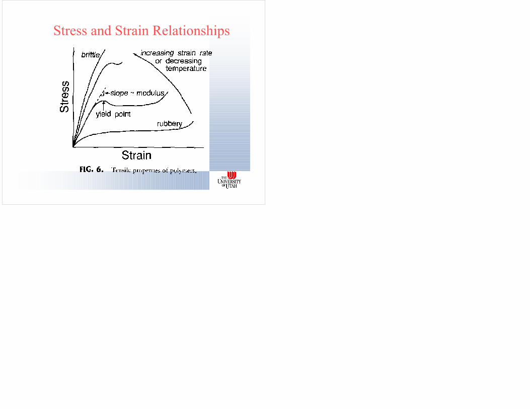
Stress and Strain Relationships
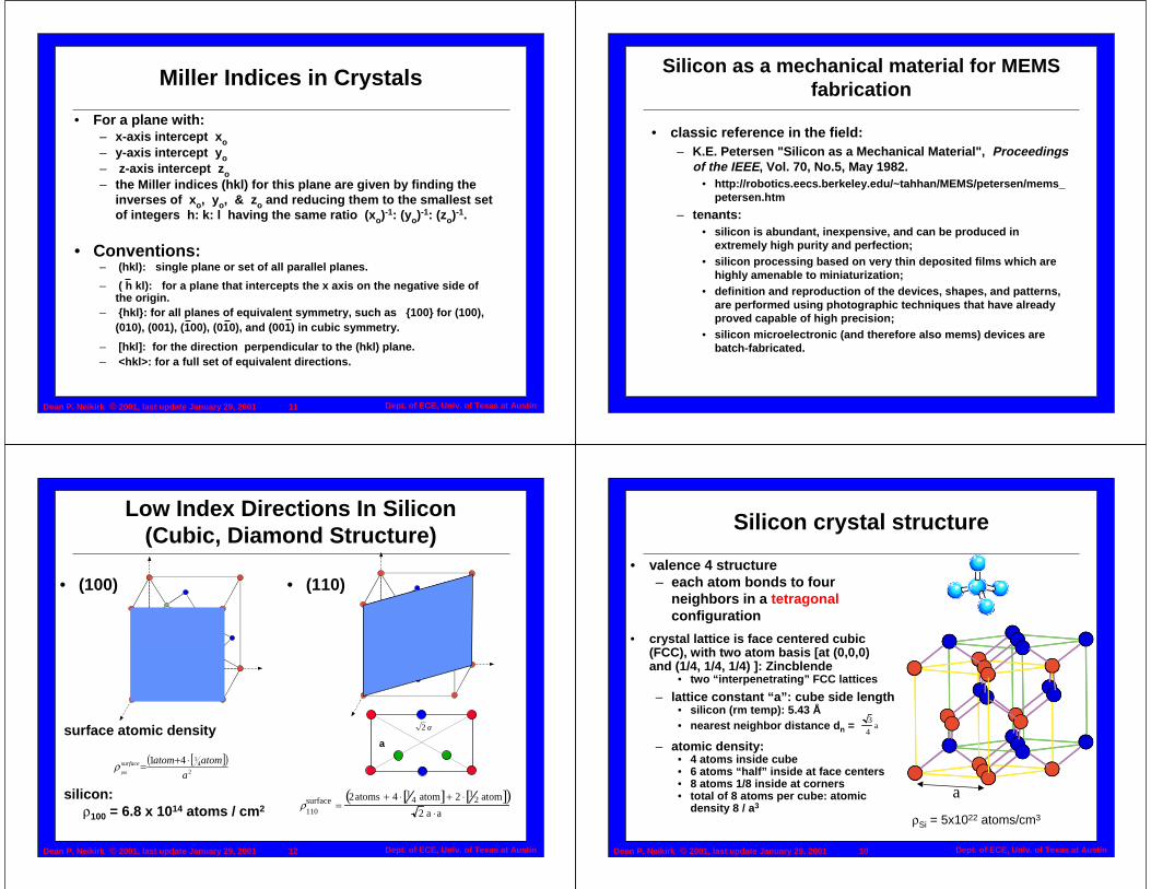
Silicon as a mechanical material for MEMS fabrication
• classic reference in the field:– K.E. Petersen "Silicon as a Mechanical Material", Proceedings
of the IEEE, Vol. 70, No.5, May 1982. • http://robotics.eecs.berkeley.edu/~tahhan/MEMS/petersen/mems_
petersen.htm
– tenants:• silicon is abundant, inexpensive, and can be produced in
extremely high purity and perfection; • silicon processing based on very thin deposited films which are
highly amenable to miniaturization; • definition and reproduction of the devices, shapes, and patterns,
are performed using photographic techniques that have already proved capable of high precision;
• silicon microelectronic (and therefore also mems) devices are batch-fabricated.
Dean P. Neikirk © 2001, last update January 29, 2001 10 Dept. of ECE, Univ. of Texas at Austin
Silicon crystal structure
• valence 4 structure– each atom bonds to four
neighbors in a tetragonalconfiguration
• crystal lattice is face centered cubic (FCC), with two atom basis [at (0,0,0) and (1/4, 1/4, 1/4) ]: Zincblende
• two “interpenetrating” FCC lattices
3
4a
– lattice constant “a”: cube side length• silicon (rm temp): 5.43 Å• nearest neighbor distance dn =
– atomic density:• 4 atoms inside cube• 6 atoms “half” inside at face centers• 8 atoms 1/8 inside at corners• total of 8 atoms per cube: atomic
density 8 / a3
ρSi = 5x10²² atoms/cm3
a
Dean P. Neikirk © 2001, last update January 29, 2001 11 Dept. of ECE, Univ. of Texas at Austin
Miller Indices in Crystals
• For a plane with:– x-axis intercept xo– y-axis intercept yo– z-axis intercept zo– the Miller indices (hkl) for this plane are given by finding the
inverses of xo, yo, & zo and reducing them to the smallest set of integers h: k: l having the same ratio (xo)-1: (yo)-1: (zo)-1.
• Conventions:– (hkl): single plane or set of all parallel planes.
– [hkl]: for the direction perpendicular to the (hkl) plane.– <hkl>: for a full set of equivalent directions.
– ( h kl): for a plane that intercepts the x axis on the negative side of the origin.
– {hkl}: for all planes of equivalent symmetry, such as {100} for (100), (010), (001), (100), (010), and (001) in cubic symmetry.
Dean P. Neikirk © 2001, last update January 29, 2001 12 Dept. of ECE, Univ. of Texas at Austin
• (100) • (110)
Low Index Directions In Silicon (Cubic, Diamond Structure)
surface atomic density
[ ]( )2
4141
100 a
atomatomsurface ⋅+=ρ
ρ110surface =
2atoms + 4 ⋅ 14 atom[ ]+ 2 ⋅ 1
2 atom[ ]( )2 a ⋅a
silicon: ρ100 = 6.8 x 10¹⁴ atoms / cm2
a
a2
Dean P. Neikirk © 2001, last update January 29, 2001 13 Dept. of ECE, Univ. of Texas at Austin
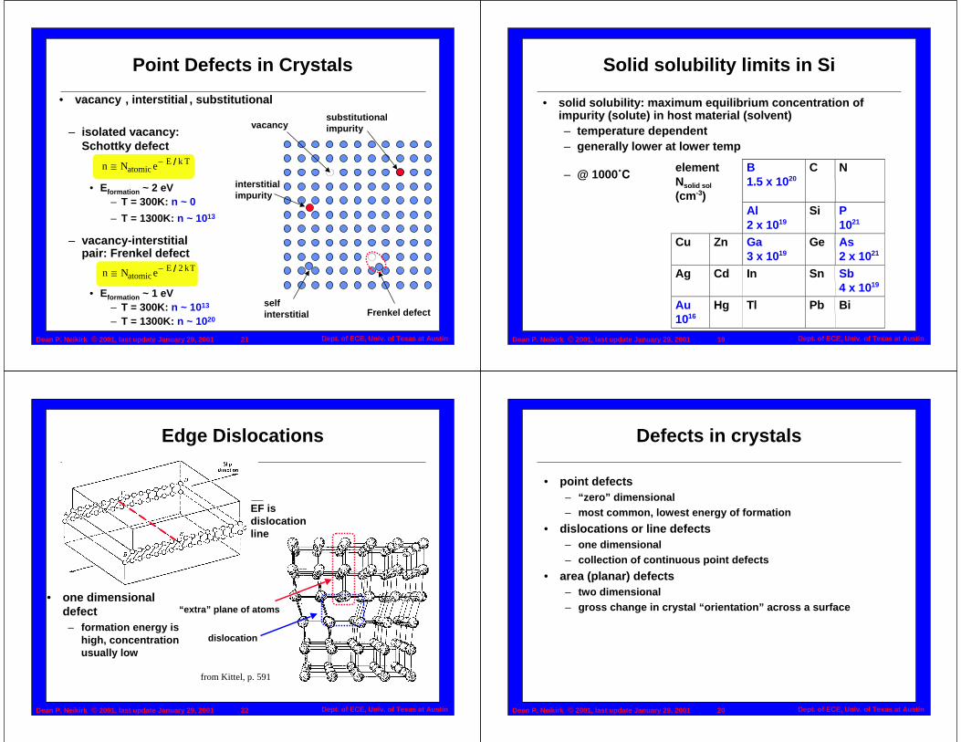
(111) planes
• (111) planes etch the slowest, tend to be cleavage planes
ρ111surface =
3 ⋅ 12 atom[ ]+ 3 ⋅ 1
6 atom[ ]( )3
2 ⋅ a2
(111) atomic plane(111) atomic plane
(100) plane
• surface atomic density somewhat higher than (100)
• silicon: 7.8 x 10¹⁴ atoms / cm2
Dean P. Neikirk © 2001, last update January 29, 2001 14 Dept. of ECE, Univ. of Texas at Austin
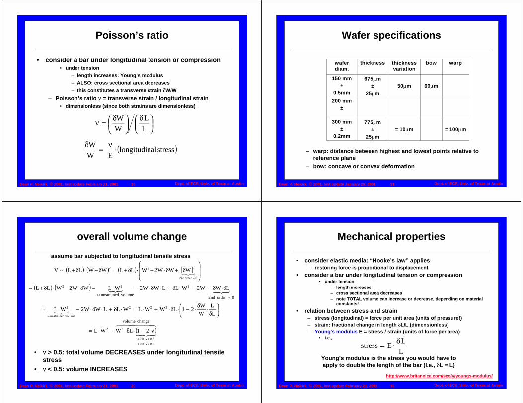
(111) orientation in silicon
• [111] is the “natural” orientation for zincblende crystals
[111] direction
(111) plane
Dean P. Neikirk © 2001, last update January 29, 2001 15 Dept. of ECE, Univ. of Texas at Austin
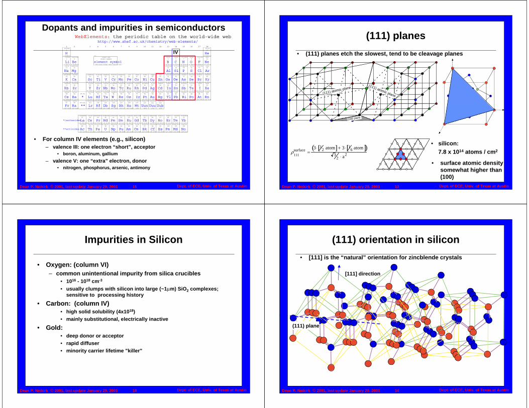
Dopants and impurities in semiconductors
1 2 3 4 5 6 7 8 9 10 11 12 13 14 15 16 17 18hydrogen helium
1 2
H He1.00794(7) Key: 4.002602(2)lithium beryllium element name boron carbon nitrogen oxygen fluorine neon
3 4 atomic number 5 6 7 8 9 10
Li Be element symbol B C N O F Ne6.941(2) 9.012182(3) 1995 atomic weight (mean relative mass) 10.811(7) 12.0107(8) 14.00674(7) 15.9994(3)18.9984032( 20.1797(6)sodium magnesium aluminium silicon phosphorus sulfur chlorine argon
11 12 13 14 15 16 17 18
Na Mg Al Si P S Cl Ar22.989770(2)24.3050(6) 26.981538(2)28.0855(3) 30.973761(2) 32.066(6) 35.4527(9) 39.948(1)potassium calcium scandium titanium vanadium chromium manganese iron cobalt nickel copper zinc gallium germanium arsenic selenium bromine krypton
19 20 21 22 23 24 25 26 27 28 29 30 31 32 33 34 35 36
K Ca Sc Ti V Cr Mn Fe Co Ni Cu Zn Ga Ge As Se Br Kr39.0983(1) 40.078(4) 44.955910(8) 47.867(1) 50.9415(1) 51.9961(6) 54.938049(9) 55.845(2) 58.933200(9)58.6934(2) 63.546(3) 65.39(2) 69.723(1) 72.61(2) 74.92160(2) 78.96(3) 79.904(1) 83.80(1)rubidium strontium yttrium zirconium niobium molybdenum technetium ruthenium rhodium palladium silver cadmium indium tin antimony tellurium iodine xenon
37 38 39 40 41 42 43 44 45 46 47 48 49 50 51 52 53 54
Rb Sr Y Zr Nb Mo Tc Ru Rh Pd Ag Cd In Sn Sb Te I Xe85.4678(3) 87.62(1) 88.90585(2) 91.224(2) 92.90638(2) 95.94(1) [98.9063] 101.07(2) 102.90550(2) 106.42(1) 107.8682(2) 112.411(8) 114.818(3) 118.710(7) 121.760(1) 127.60(3) 126.90447(3) 131.29(2)caesium barium lutetium hafnium tantalum tungsten rhenium osmium iridium platinum gold mercury thallium lead bismuth polonium astatine radon
55 56 57-70 71 72 73 74 75 76 77 78 79 80 81 82 83 84 85 86
Cs Ba * Lu Hf Ta W Re Os Ir Pt Au Hg Tl Pb Bi Po At Rn132.90545(2)137.327(7) 174.967(1) 178.49(2) 180.9479(1) 183.84(1) 186.207(1) 190.23(3) 192.217(3) 195.078(2) 196.96655(2) 200.59(2) 204.3833(2) 207.2(1) 208.98038(2) [208.9824] [209.9871] [222.0176]francium radium lawrencium rutherfordiumdubnium seaborgium bohrium hassium meitnerium ununnilium unununium ununbium
87 88 89-102 103 104 105 106 107 108 109 110 111 112
Fr Ra ** Lr Rf Db Sg Bh Hs Mt Uun Uuu Uub[223.0197] [226.0254] [262.110] [261.1089] [262.1144] [263.1186] [264.12] [265.1306] [268] [269] [272] [277]
lanthanum cerium praseodymiu neodymium promethium samarium europium gadolinium terbium dysprosium holmium erbium thulium ytterbium
57 58 59 60 61 62 63 64 65 66 67 68 69 70
*lanthanidesLa Ce Pr Nd Pm Sm Eu Gd Tb Dy Ho Er Tm Yb138.9055(2) 140.116(1) 140.90765(2) 144.24(3) [144.9127] 150.36(3) 151.964(1) 157.25(3) 158.92534(2) 162.50(3) 164.93032(2) 167.26(3) 168.93421(2) 173.04(3)actinium thorium protactinium uranium neptunium plutonium americium curium berkelium californiumeinsteinium fermium mendelevium nobelium
89 90 91 92 93 94 95 96 97 98 99 100 101 102
**actinides Ac Th Pa U Np Pu Am Cm Bk Cf Es Fm Md No[227.0277] 232.0381(1)231.03588(2)238.0289(1) [237.0482] [244.0642] [243.0614] [247.0703] [247.0703] [251.0796] [252.0830] [257.0951] [258.0984] [259.1011]
WebElements: the periodic table on the world-wide webhttp://www.shef.ac.uk/chemistry/web-elements/
Symbols and names: the symbols of the elements, their names, and their spellings are those recommended by IUPAC. After some controversy, the names of elements 101-109 are now confirmed: see Pure & Appl. Chem., 1997, 69, 2471–2473. Names have not been proposed as yet for the most relements 110–112 so those used here are IUPAC’s temporary systematic names: see Pure & Appl. Chem., 1979, 51, 381–384. In the USA and some other countries, the spellings aluminum and cesium are normal while in the UK and elsewhere the usual spelling is sulPeriodic table organisation: for a justification of the positions of the elements La, Ac, Lu, and Lr in the WebElements periodic table see W.B. Jensen, “The positions of lanthanum (actinium) and lutetium (lawrencium) in the periodic table”,Group labels: the numeric system (1–18) used here is the current IUPAC convention. For a discussion of this and other common systems see: W.C. Fernelius and W.H. Powell, “Confusion in the periodic table of the elements”, J. Chem. Ed., 1959, 504–508.Atomic weights (mean relative masses): see Pure & Appl. Chem., 1996, 68, 2339–2359. These are the IUPAC 1995 values. Elements for which the atomic weight is contained within square brackets have no stable nuclides and are represented by one of the elements thorium, protactinium, and uranium do have characteristic terrestrial abundances and these are the values quoted. The last significant figure of each value is considered reliable to ±1 except where a larger uncertainty is giv©1998 Dr Mark J Winter [University of Sheffield, [email protected]]. For updates to this table see http://www.shef.ac.uk/chemistry/web-elements/pdf/periodic-table.html. Version date: 1 March 1998.
IV
• For column IV elements (e.g., silicon)– valence III: one electron “short”, acceptor
• boron, aluminum, gallium
– valence V: one “extra” electron, donor• nitrogen, phosphorus, arsenic, antimony
Dean P. Neikirk © 2001, last update January 29, 2001 18 Dept. of ECE, Univ. of Texas at Austin
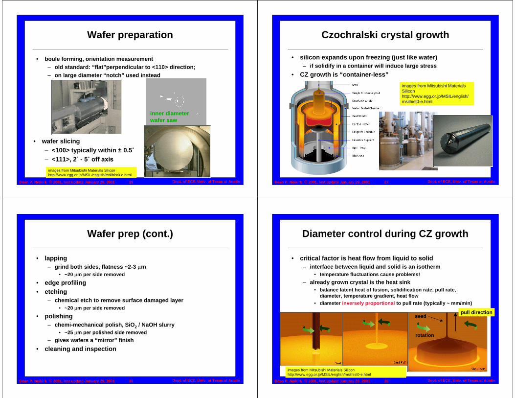
Impurities in Silicon
• Oxygen: (column VI)– common unintentional impurity from silica crucibles
• 1016 - 1018 cm-3
• usually clumps with silicon into large (~1µm) SiO2 complexes; sensitive to processing history
• Carbon: (column IV)• high solid solubility (4x10¹⁸)• mainly substitutional, electrically inactive
• Gold:• deep donor or acceptor• rapid diffuser• minority carrier lifetime "killer"
Dean P. Neikirk © 2001, last update January 29, 2001 19 Dept. of ECE, Univ. of Texas at Austin
Solid solubility limits in Si
• solid solubility: maximum equilibrium concentration of impurity (solute) in host material (solvent)– temperature dependent– generally lower at lower temp
– @ 1000��elementNsolid sol
(cm-3)
B1.5 x 1020
C N
Al2 x 1019
Si P1021
Cu Zn Ga3 x 1019
Ge As2 x 1021
Ag Cd In Sn Sb4 x 1019
Au1016
Hg Tl Pb Bi
Dean P. Neikirk © 2001, last update January 29, 2001 20 Dept. of ECE, Univ. of Texas at Austin
Defects in crystals
• point defects– “zero” dimensional– most common, lowest energy of formation
• dislocations or line defects– one dimensional– collection of continuous point defects
• area (planar) defects– two dimensional– gross change in crystal “orientation” across a surface
Dean P. Neikirk © 2001, last update January 29, 2001 21 Dept. of ECE, Univ. of Texas at Austin
Point Defects in Crystals
• vacancy
n ≅ Natomic e− E k T
n ≅ Natomic e− E 2 kT
• Eformation ~ 2 eV– T = 300K: n ~ 0
– T = 1300K: n ~ 1013
– vacancy-interstitial pair: Frenkel defect
• Eformation ~ 1 eV– T = 300K: n ~ 1013
– T = 1300K: n ~ 1020
– isolated vacancy: Schottky defect
, substitutional, interstitial
vacancysubstitutionalimpurity
interstitial impurity
self interstitial Frenkel defect
Dean P. Neikirk © 2001, last update January 29, 2001 22 Dept. of ECE, Univ. of Texas at Austin
Edge Dislocations
from Kittel, p. 591
“extra” plane of atoms
dislocation
• one dimensional defect– formation energy is
high, concentration usually low
EF is dislocation line

Dean P. Neikirk © 2001, last update January 29, 2001 23 Dept. of ECE, Univ. of Texas at Austin
Screw Dislocation (1-d defect)
• screw dislocations are most commonly formed during crystal growth
Dean P. Neikirk © 2001, last update January 29, 2001 24 Dept. of ECE, Univ. of Texas at Austin
• planar (2-d) defect– stacking fault:
missing or extra (111) plane
• A - B - C - C - A - B - C• A - B - A - B - C
Stacking arrangement and stacking faults
• layer ordering:
A B C A B C
A
B
C
A
Dean P. Neikirk © 2001, last update January 29, 2001 25 Dept. of ECE, Univ. of Texas at Austin
Bulk crystal growth
• melting points– silicon: 1420���– quartz: 1732���
• starting material: metallurgical-grade silicon– by mixing with carbon, SiO2 reduced in arc furnace
• T > 1780�������SiC + SiO2 → Si + SiO + CO
– common impurities• Al: 1600 ppm (1 ppm = 5 x 1016 cm-3)• B: 40 ppm• Fe: 2000 ppm• P: 30 ppm
– used mostly as an additive in steel
Dean P. Neikirk © 2001, last update January 29, 2001 26 Dept. of ECE, Univ. of Texas at Austin
Preparation of electronic-grade silicon
• gas phase purification used to produce high purity silicon– ~ 600��– crud + Si + HCl →
• SiCl4 (silicon tetrachloride)• SiCl3H (trichlorosilane)• SiCl2H2 (dichlorosilane)• chlorides of impurities
– trichlorosilane (liquid at rm temp), further purification via fractional distillation
• now reverse reaction– 2SiHCl3 + 2H2 (heat) → 2Si + 6HCl– after purification get
• Al: below detection• B: < 1 ppb (1 ppb = 5 x 1013 cm-3)• Fe: 4 ppm• P: < 2 ppb• Sb: 1 ppb• Au: 0.1 ppb
Dean P. Neikirk © 2001, last update January 29, 2001 27 Dept. of ECE, Univ. of Texas at Austin
Czochralski crystal growth
• silicon expands upon freezing (just like water)– if solidify in a container will induce large stress
• CZ growth is “container-less”
images from Mitsubishi Materials Siliconhttp://www.egg.or.jp/MSIL/english/msilhist0-e.html
Dean P. Neikirk © 2001, last update January 29, 2001 28 Dept. of ECE, Univ. of Texas at Austin
Diameter control during CZ growth
• critical factor is heat flow from liquid to solid– interface between liquid and solid is an isotherm
• temperature fluctuations cause problems!
– already grown crystal is the heat sink• balance latent heat of fusion, solidification rate, pull rate,
diameter, temperature gradient, heat flow• diameter inversely proportional to pull rate (typically ~ mm/min)
images from Mitsubishi Materials Siliconhttp://www.egg.or.jp/MSIL/english/msilhist0-e.html
pull directionseed
rotation
Dean P. Neikirk © 2001, last update January 29, 2001 29 Dept. of ECE, Univ. of Texas at Austin
Wafer preparation
• boule forming, orientation measurement– old standard: “flat”perpendicular to <110> direction; – on large diameter “notch” used instead
images from Mitsubishi Materials Siliconhttp://www.egg.or.jp/MSIL/english/msilhist0-e.html
inner diameter wafer saw
• wafer slicing– <100> typically within ± 0.5�– <111>, 2��- 5��������
Dean P. Neikirk © 2001, last update January 29, 2001 30 Dept. of ECE, Univ. of Texas at Austin
Wafer prep (cont.)
• lapping– grind both sides, flatness ~2-3 µm
• ~20 µm per side removed
• edge profiling• etching
– chemical etch to remove surface damaged layer• ~20 µm per side removed
• polishing– chemi-mechanical polish, SiO2 / NaOH slurry
• ~25 µm per polished side removed
– gives wafers a “mirror” finish
• cleaning and inspection
Dean P. Neikirk © 2001, last update January 29, 2001 31 Dept. of ECE, Univ. of Texas at Austin
Wafer specifications
– warp: distance between highest and lowest points relative to reference plane
– bow: concave or convex deformation
wafer diam.
thickness thickness variation
bow warp
150 mm ±
0.5mm
675µm ±
25µm
50µm
60µm
200 mm ±
300 mm ±
0.2mm
775µm ±
25µm
= 10µm
= 100µm
Dean P. Neikirk © 2001, last update February 21, 2001 18 Dept. of ECE, Univ. of Texas at Austin
Mechanical properties
• consider elastic media: “Hooke’s law” applies– restoring force is proportional to displacement
• consider a bar under longitudinal tension or compression• under tension
– length increases– cross sectional area decreases– note TOTAL volume can increase or decrease, depending on material
constants!
• relation between stress and strain– stress (longitudinal) = force per unit area (units of pressure!)– strain: fractional change in length δL/L (dimensionless)– Young’s modulus E = stress / strain (units of force per area)
• i.e.,
L
LEstress
δ⋅=
http://www.britannica.com/seo/y/youngs-modulus/
Young’s modulus is the stress you would have to apply to double the length of the bar (I.e., δL = L)
Dean P. Neikirk © 2001, last update February 21, 2001 19 Dept. of ECE, Univ. of Texas at Austin
Poisson’s ratio
• consider a bar under longitudinal tension or compression• under tension
– length increases: Young’s modulus– ALSO: cross sectional area decreases– this constitutes a transverse strain δW/W
– Poisson’s ratio ν = transverse strain / longitudinal strain• dimensionless (since both strains are dimensionless)
δ
δ=ν
LL
WW
( )stressallongitudinEW
W ⋅ν=δ
Dean P. Neikirk © 2001, last update February 21, 2001 20 Dept. of ECE, Univ. of Texas at Austin
overall volume change
• ν > 0.5: total volume DECREASES under longitudinal tensile stress
• ν < 0.5: volume INCREASES
( ) ( ) ( ) [ ]
δ+δ⋅−⋅δ+=δ−⋅δ+∝
≈���
0ordernd2
222 WWW2WLLWWLLV
( ) ( )��������
0ordernd2volumeunstrained
LWW2WLLWW2WLWW2WLL 222
≈∝δ⋅δ⋅−⋅δ+⋅δ⋅−⋅=δ⋅−⋅δ+≈
δ⋅δ⋅−⋅δ⋅+⋅=⋅δ+⋅δ⋅−⋅≈
∝ L
L
W
W21LWWLWLLWW2WL 222
volumeunstrained
2���
( )��� ���� ��
�����
changevolume
5.0if0
5.0if0
22 21LWWL
<ν>>ν<
ν⋅−⋅δ⋅+⋅=
assume bar subjected to longitudinal tensile stress
Dean P. Neikirk © 2001, last update February 21, 2001 21 Dept. of ECE, Univ. of Texas at Austin
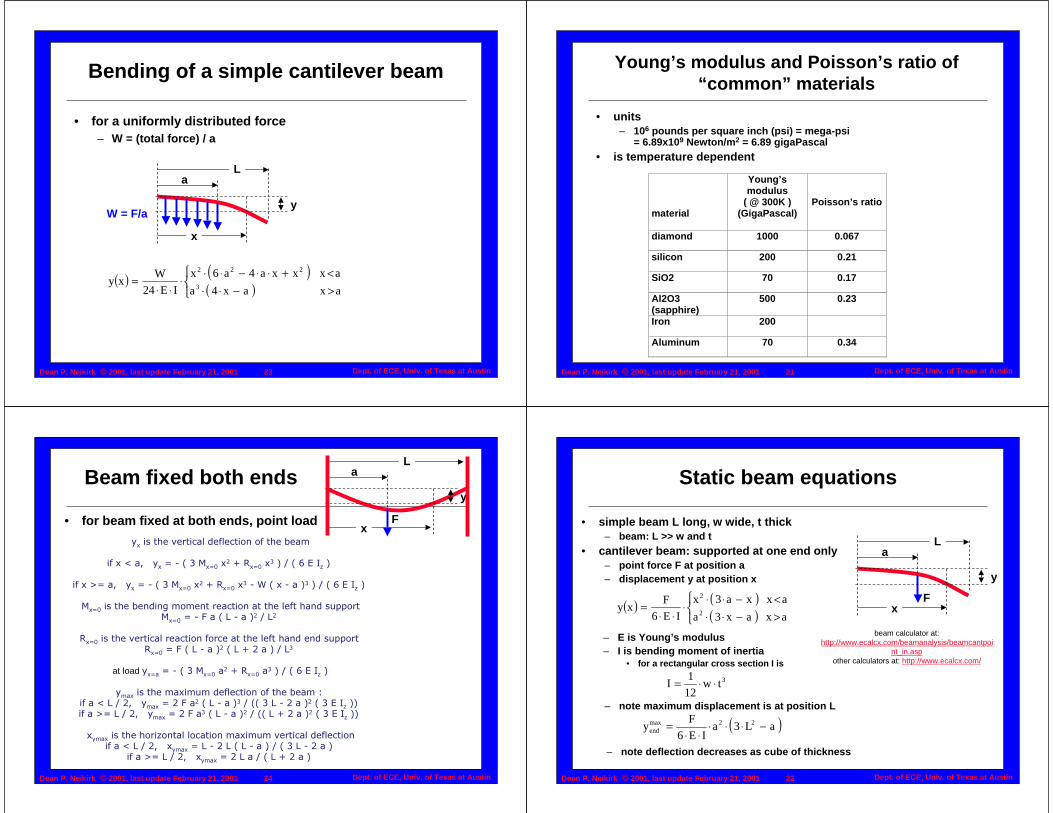
Young’s modulus and Poisson’s ratio of “common” materials
• units– 106 pounds per square inch (psi) = mega-psi
= 6.89x10⁹ Newton/m2 = 6.89 gigaPascal• is temperature dependent
material
Young’s modulus
( @ 300K ) (GigaPascal)
Poisson’s ratio
diamond 1000 0.067
silicon 200 0.21
SiO2 70 0.17
Al2O3 (sapphire)
500 0.23
Iron 200
Aluminum 70 0.34
Dean P. Neikirk © 2001, last update February 21, 2001 22 Dept. of ECE, Univ. of Texas at Austin
Static beam equations
• simple beam L long, w wide, t thick– beam: L >> w and t
• cantilever beam: supported at one end only– point force F at position a– displacement y at position x
( )aL3aIE6
Fy 22max
end −⋅⋅⋅⋅⋅
=
3tw12
1I ⋅⋅=
y
La
Fx( ) ( )
( )
>−⋅⋅<−⋅⋅
⋅⋅⋅
=axax3a
axxa3x
IE6
Fxy
2
2
– E is Young’s modulus– I is bending moment of inertia
• for a rectangular cross section I is
– note maximum displacement is at position L
beam calculator at: http://www.ecalcx.com/beamanalysis/beamcantpoi
nt_in.aspother calculators at: http://www.ecalcx.com/
– note deflection decreases as cube of thickness
Dean P. Neikirk © 2001, last update February 21, 2001 23 Dept. of ECE, Univ. of Texas at Austin
Bending of a simple cantilever beam
• for a uniformly distributed force– W = (total force) / a
( ) ( )( )
>−⋅⋅<+⋅⋅−⋅⋅
⋅⋅⋅
=axax4a
axxxa4a6x
IE24
Wxy
3
222
y
La
W = F/a
x
Dean P. Neikirk © 2001, last update February 21, 2001 24 Dept. of ECE, Univ. of Texas at Austin
Beam fixed both ends
• for beam fixed at both ends, point load
y
La
Fx
�� ������������ ���� ������������������
��������� �� ��� �������� �� ������ �� �� ���!�"�#$ ��
�����%���� �� ��� �������� �� ������ �� � &������ ���� �� ���!�"�#$ ��
���� �������������'����������������������� ����������())������ ��� *�����+�� ���� �+�
���� ������������ ��������������������� ��������������())������� ��*���+�� ���� ��+��������� �+�
at load ���� ��� �������� �� ������ �� �� ���!�"�#$ �
���� ������������(����� �������������������,��������+� ��� ���� ����*��� ��+�� ���� ������+�� ������ ����"�#$ ��������%��+� ��� ���� ����*��� ��+�� ���� ����+��������� ����"�#$ ���
����� ����������$���� � �������������(������� ���� �������������+� ��� ����� ��+�� ��+���+�� ���� �����+�� ������
�����%��+� ��� ����� ����+��� ���+���������
Dean P. Neikirk © 2001, last update February 21, 2001 25 Dept. of ECE, Univ. of Texas at Austin
Beam fixed both ends
• for beam fixed at both ends, distributed uniform load to a����������� ������������ ���� �����������������������,
��������� �� ��� �������� �� ������ �� � -��. �.��� ���!�"�#$ ��
�����%���� �� ��� �������� �� ������ �� � -��. �.���-������ ���. �.��� ���!�"�#$ �
���� �������������'������������������� �����())��,����� �����+ +������+� -��� ���
���� ������������ ��������������������� �����())��,����� ��-���� ���+
���+ ������������ ���������������'����())��,����+ ��-��� ����+�� ���� ���+�
y
La
W = F/ax
Dean P. Neikirk © 2001, last update February 21, 2001 26 Dept. of ECE, Univ. of Texas at Austin
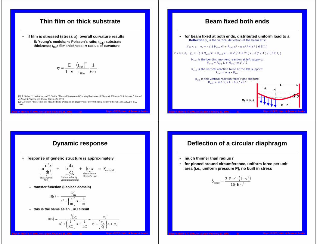
Deflection of a circular diaphragm
• much thinner than radius r• for pinned around circumference, uniform force per unit
area (i.e., uniform pressure P), no built in stress
( )3
24
center tE16
1rP3
⋅⋅ν−⋅⋅⋅=δ
Dean P. Neikirk © 2001, last update February 21, 2001 27 Dept. of ECE, Univ. of Texas at Austin
Thin film on thick substrate
• if film is stressed (stress σ), overall curvature results– E: Young’s moduls; ν: Poisson’s ratio; tsub: substrate
thickness; tfilm: film thickness; r: radius of curvature
( )r6
1
t
t
1
E
film
2sub
⋅⋅⋅
ν−≈σ
[1] A. Sinha, H. Levinstein, and T. Smith, “Thermal Stresses and Cracking Resistance of Dielectric Films on Si Substrates,” Journal of Applied Physics, vol. 49, pp. 2423-2426, 1978.[2] G. Stoney, “The Tension of Metallic Films Deposited by Electrolysis,” Proceedings of the Royal Society, vol. A82, pp. 172, 1909.
Dean P. Neikirk © 2001, last update February 21, 2001 28 Dept. of ECE, Univ. of Texas at Austin
Dynamic response
• response of generic structure is approximately
�� external
laws’Hookeforceelastic
dampingviscousvelocityforce
NSLaccel*mass
2
2
Fxkdt
dxb
dt
xdm =⋅++
∝���
( )mk
smb
s
m1
sH2 +⋅
+
=
( )2
oo2
2o
2 sQ
sLC1
sRC1
s
LC1
sH
ω+⋅
ω+
ω=+⋅
+
=
– transfer function (Laplace domain)
– this is the same as an LRC circuit