Basic I/O Interface - 8255 -...
17
Basic I/O Interface - 8255
Transcript of Basic I/O Interface - 8255 -...
Basic I/O Interface - 8255

11–3 THE PROGRAMMABLE PERIPHERAL
• 82C55 programmable peripheral interface (PPI) is a popular,
low-cost interface component found in many applications.
• The PPI has 24 pins for I/O, programmable in groups of 12 pins
and groups that operate in three distinct modes of operation.
• 82C55 can interface any TTL-compatible
I/O device to the microprocessor.
2

• The 82C55 (CMOS version) requires wait states if
operated with a processor using higher than an 8
MHz clock.
• also provides at least 2.5 mA of sink (logic 0)
current at each output, a maximum of 4.0 mA
• Because I/O devices are inherently slow, wait states
used during I/O transfers do not impact significantly
upon the speed of the system.
• The 82C55 still finds application even in the latest
Core2-based computer system.
3

• 82C55 is used for interface to the keyboard and parallel printer port in many PCs.
• found as a function within an interfacing chip set
• also controls the timer and reads data from the keyboard interface
• An experimentation board is available that plugs into the parallel port of a PC, to allow access to an 8255 located on the board.
• The 8255 is programmed in either assembly language or Visual C++ through drivers available with the board.
4
Basic Description of the 82C55
• Fig 11–18 shows pin-outs of the 82C55 in
DIP and surface mount (flat pack) format.
• The three I/O ports (labeled A, B, and C) are programmed as
groups.
• group A connections consist of port A (PA7–PA0) and the upper half of port
C (PC7–PC4)
• group B consists of port B (PB7–PB0) and the lower half of port C (PC3–
PC0)
• 82C55 is selected by its CS pin for programming and
reading/writing to a port.
5

Figure 11–18 The pin-out of the 82C55
peripheral interface adapter (PPI).
6

• Table 11–2 shows I/O port assignments used for programming
and access to the I/O ports.
• In the PC, a pair of 82C55s, or equivalents, are decoded at I/O
ports 60H–63H and also
at ports 378H–37BH.
• The 82C55 is a fairly simple device to interface to the
microprocessor and program.
• For 82C55 to be read or written, the CS input must be logic 0
and the correct I/O address must be applied to the A1 and A0
pins.
• Remaining port address pins are don’t cares.
7
• Fig 11–19 shows an 82C55 connected to the 80386SX so it
functions at 8-bit addresses C0H (port A), C2H (port B), C4H
(port C),
and C6H (command register).
• this interface uses the low bank of the I/O map
• All 82C55 pins are direct connections to the 80386SX, except
the CS pin. The pin is decoded/selected by a 74ALS138
decoder.
• A RESET to 82C55 sets up all ports as
simple input ports using mode 0 operation.
• initializes the device when the processor is reset
8

Figure 11–19 The 82C55 interfaced to the low bank of the
80386SX microprocessor.
9

• After a RESET, no other commands are needed, as
long as it is used as an input device for all three
ports.
• 82C55 is interfaced to the PC at port addresses 60H–
63H for keyboard control.
• also for controlling the speaker, timer, and other internal
devices such as memory expansion
• It is also used for the parallel printer port at I/O ports
378H–37BH.
10
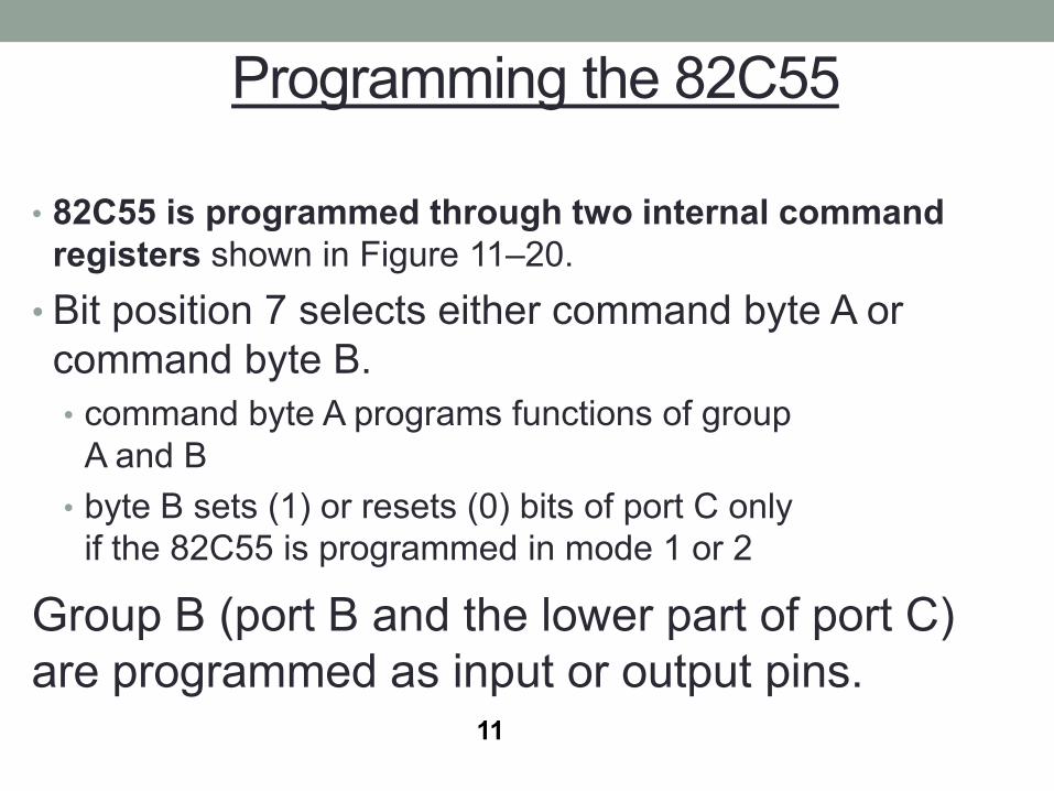
Programming the 82C55
• 82C55 is programmed through two internal command
registers shown in Figure 11–20.
• Bit position 7 selects either command byte A or
command byte B.
• command byte A programs functions of group
A and B
• byte B sets (1) or resets (0) bits of port C only
if the 82C55 is programmed in mode 1 or 2
11
Group B (port B and the lower part of port C)
are programmed as input or output pins.
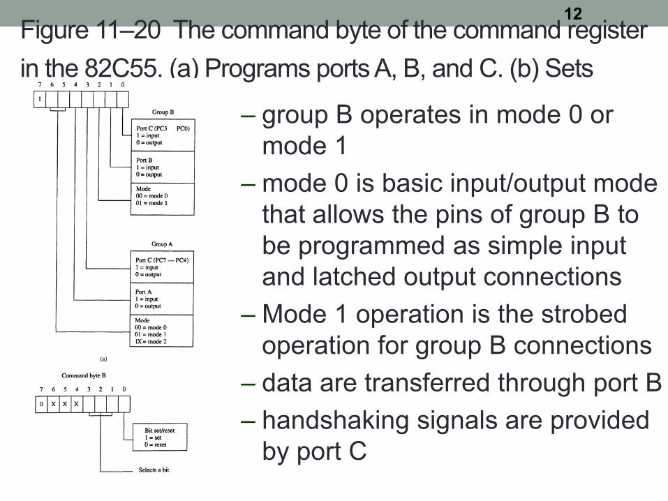
Figure 11–20 The command byte of the command register
in the 82C55. (a) Programs ports A, B, and C. (b) Sets or
resets the bit indicated in the select a bit field.
12
– group B operates in mode 0 or
mode 1
– mode 0 is basic input/output mode
that allows the pins of group B to
be programmed as simple input
and latched output connections
– Mode 1 operation is the strobed
operation for group B connections
– data are transferred through port B
– handshaking signals are provided
by port C
• Group A (port A and the upper part of port C) are
programmed as input or output pins.
• Group A can operate in modes 0, 1, and 2.
• mode 2 operation is a bidirectional mode of operation for
port A
• If a 0 is placed in bit position 7 of the command byte,
command byte B is selected
• This allows any bit of port C to be set (1) or reset (0),
if the 82C55 is operated in either mode 1 or 2.
• otherwise, this byte is not used for programming
13
Mode 0 Operation
• Mode 0 operation causes 82C55 to function:
• as a buffered input device
• as a latched output device
• Fig 11–21 shows 82C55 connected to a
set of eight seven-segment LED displays.
• These are standard LEDs.
• the interface can be modified with a change
in resistor values for an organic LED (OLED) display or high-
brightness LEDs
14
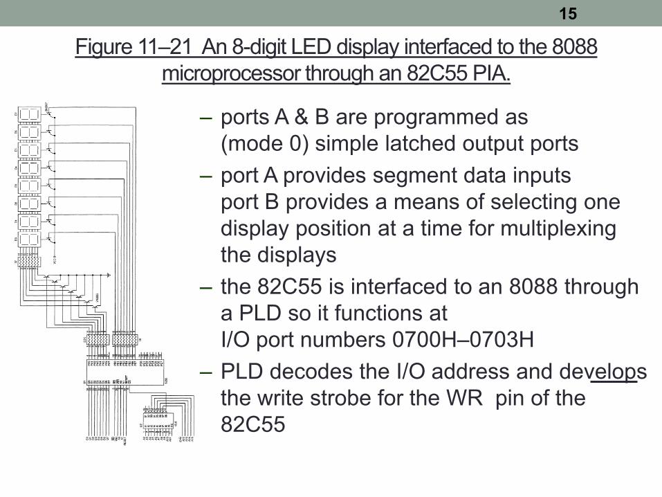
Figure 11–21 An 8-digit LED display interfaced to the 8088
microprocessor through an 82C55 PIA.
15
– ports A & B are programmed as
(mode 0) simple latched output ports
– port A provides segment data inputs
port B provides a means of selecting one
display position at a time for multiplexing
the displays
– the 82C55 is interfaced to an 8088 through
a PLD so it functions at
I/O port numbers 0700H–0703H
– PLD decodes the I/O address and develops
the write strobe for the WR pin of the
82C55
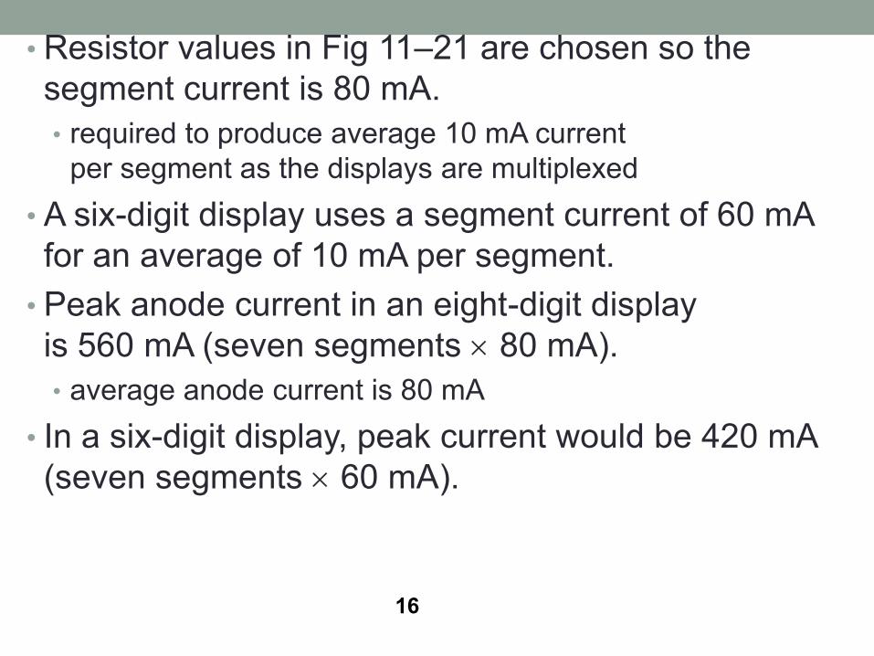
• Resistor values in Fig 11–21 are chosen so the
segment current is 80 mA.
• required to produce average 10 mA current
per segment as the displays are multiplexed
• A six-digit display uses a segment current of 60 mA
for an average of 10 mA per segment.
• Peak anode current in an eight-digit display
is 560 mA (seven segments 80 mA).
• average anode current is 80 mA
• In a six-digit display, peak current would be 420 mA
(seven segments 60 mA).
16
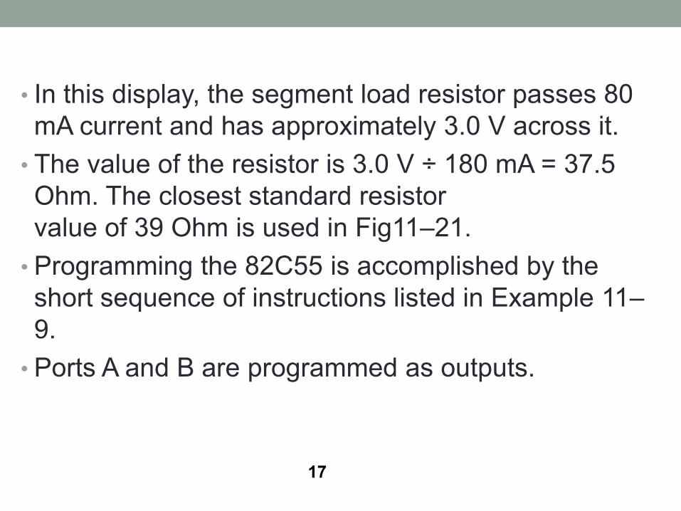
• In this display, the segment load resistor passes 80
mA current and has approximately 3.0 V across it.
• The value of the resistor is 3.0 V ÷ 180 mA = 37.5
Ohm. The closest standard resistor
value of 39 Ohm is used in Fig11–21.
• Programming the 82C55 is accomplished by the
short sequence of instructions listed in Example 11–
9.
• Ports A and B are programmed as outputs.
17