
Basic concepts in CACHING - unipvBasic concepts in CACHING • Cache basic operation ... – Memory...
74
Basic concepts in CACHING • Cache basic operation • Direct-Mapped and Set-Associative cache • Multiple-level caching 1
Transcript of Basic concepts in CACHING - unipvBasic concepts in CACHING • Cache basic operation ... – Memory...

Basic concepts in CACHING
• Cache basic operation
• Direct-Mapped and Set-Associative cache
• Multiple-level caching
1
CPU and main memory
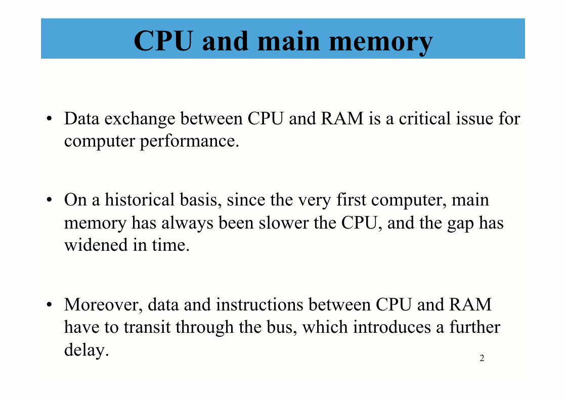
• Data exchange between CPU and RAM is a critical issue for computer performance.
• On a historical basis, since the very first computer, main memory has always been slower the CPU, and the gap has widened in time.
• Moreover, data and instructions between CPU and RAM have to transit through the bus, which introduces a further delay. 2

CPU and main memory • Performance ratio of CPU vs RAM in time, with ratio 1 in 1980
(Hennessy-Patterson, Fig. 5.2). RAM increase: ~ 7% per year. CPU: ~25% per year until 1986, ~52% until 2000, ~52% up to 2005, 0% later .
3 Copyright © 2011, Elsevier Inc. All rights Reserved.

CPU and main memory
• Clearly, it is useless building ever speedier and sophisticated processors, if instructions to be executed and data to be worked on cannot be fetched as quickly.
• In datapaths considered so far, the assumption was that the Instruction Memory and the Data Memory would run at the same speed as the other pipeline components.
• This assumptions actually requires a very complex system to manage information flow between CPU and RAM.
4
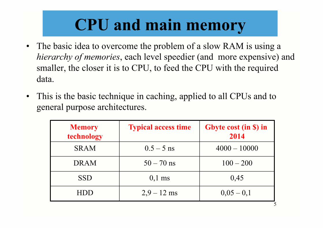
CPU and main memory • The basic idea to overcome the problem of a slow RAM is using a
hierarchy of memories, each level speedier (and more expensive) and smaller, the closer it is to CPU, to feed the CPU with the required data.
• This is the basic technique in caching, applied to all CPUs and to general purpose architectures.
Memory technology
Typical access time Gbyte cost (in $) in 2014
SRAM 0.5 – 5 ns 4000 – 10000
DRAM 50 – 70 ns 100 – 200
SSD 0,1 ms 0,45
HDD 2,9 – 12 ms 0,05 – 0,1 5

Caching
• The caching technique is not typical of the CPU-RAM relationship, it is very basic and applies to the whole memory subsystem in a computer:
– Registers act as a cache to the actual hw cache
– The hw cache acts as a cache to RAM
– RAM acts as a cache to the hard disk (virtual memory)
– The hard disk acts as a cache to slower magnetic devices
6

Caching • Here is a sound relationship among memories, capacities
and speed (Hennessy-Patterson, Fig. 5.1):
7

Caching • A more detailed case: server and PMD (H-P5, Fig. 2.1):
8
Copyright © 2011, Elsevier Inc. All rights Reserved.

Caching
• The concept of the cache was born together with that of computer:
• Ideally, one would desire an indefinitely large memory capacity such that any particular...word would be immediately available...We are forced to recognize the possibility of constructing a hierarchy of memories, each which has greater capacity than the preceding but which is less quickly accessible
A. Burks, H. Goldstine, J. von Neumann Preliminary Discussion of the logical Design of Electronic Computing Instrument (1946)
9

Caching
• Even if the cache concept dates as early as the Von Neuman type of computer, only in the late 60s were produced the first CPU equipped with a true cache.
• The basic idea is well understood: a cache is a small, but speedy memory holding part of the data available in RAM.
• If data and instructions required by the CPU are found to a great percentage in the cache, the performance penalty due to slow access to RAM is reduced dramatically.
10

Caching • Current CPUs have separate caches for data and for instructions. With
this architecture, in a pipelined datapath, it is possible, within the same clock cycle:
– to fetch an instruction from the instruction cache (I-cache), that we have so far called the Instruction Memory, and
– to load/to store data (for a different instruction) from/to the data cache (D-cache), that we have so far called Data Memory.
• I-cache and D-cache together are the first-level cache (L1).
• Most processors have a second-level cache (L2) as well, and there are even processors with a third-level cache (L3).
11
Cache locality • Caches yield great advantages because the principle of
locality holds in most cases, in two modes:
• Spatial locality:
– Memory items at addresses near items just referenced will be referenced in close time (as an instance, instructions are executed in sequence, and array elementes are read/written in sequence as well).
• Temporal Locality:
– Memory items recently addressed are likely to be referenced again in the near future (e.g. instructions and variables within a loop).
12

Cache basic operation • N.B. Here we only consider read operations from RAM. Later we will
cover also operations involving a modification of the data.
• For the purpose of operating with a cache, RAM is split into fixed-size blocks name cache lines (or simply lines) or cache blocks (or simply blocks).
– A block contains a fixed number of consecutive bytes of RAM (4 to 256, according to implementations, always a power of 2)
• Blocks are numbered consecutively starting from 0, so with 32-byte blocks we have:
– block 0: RAM bytes from 0 to 31 – block 1: RAM bytes from 32 to 63 – block 2: RAM bytes from 64 to 95
13
Cache basic operation • Each block is identified with its address in RAM, which is
the RAM address of the first byte in the block.
• Since blocks contain 2m bytes, each block address has the following pattern:
x x … x x 0 0 … 0 0
• Question: what is the relationship between the number of a block and its address?
14
m bits

Basic cache operation • At any time, some RAM blocks are in the cache too (we assume first-
level only caches, separate for instructions and for data, working at roughly the same speed as the CPU).
• When a word (for an integer, or an instruction in 4 bytes) is addressed, the hardware checks if the word is in the cache too.
• If so, this is a cache hit and every thing goes on normally, since the cache can work at the same speed of the other datapath components.
• If not, this is a cache miss: (the block containing) the missing data is fetched from RAM. Occasionally, a block must be removed from the cache, to accommodate for the new (missing) one.
15

Direct-mapped cache
• Direct-Mapped caches are the most simple ones. A direct-mapped cache consists of 2n entries, with consecutive numbers.
• Each entry stores a block: 2m consecutive bytes from RAM (usually 2m = 32 or 64). Each entry has two information with it:
1. a validity bit for the entry
2. a tag that uniquely identifies the block stored in the cache with respect to RAM
• As an instance, a 2048-entry cache, each 32-byte, contains overall 2048 x 32 = 64KB of data (or instructions)
16

Direct-mapped cache • In a direct-mapped cache, each RAM block is stored in a
single cache location.
• So, given a memory address, there is a single precise position in the cache where to look for. If it is in the cache, it is there.
• To find the cache location containing the RAM block holding the addressed data or instruction, the computation is:
(block address in RAM) modulo (number of entries in the cache)
• The computation is straightforward if the number of cache entries is a power of 2 17
what is a “block address”?

Direct-mapped cache • The PC, a LOAD or a STORE specify a word address to be
accessed (an instruction addressed by the PC, or a data item for reading or writing).
• How can we get the RAM address of the block holding that peculiar word?
• Once obtained that address, how can we check if the block is already in the cache?
• And if the block is in the cache, how do we get the word on the basis of the address specified through the PC, LOAD or STORE?
18

Direct-mapped cache • (Patterson-Henessy, fig. 7.5).
As as example, let us assume a RAM split into 32 blocks one byte each, and an 8-entry cache (a byte each entry, of course).
• In which cache entry is stored the block with address 01001?
19
• 01001 mod 1000 = 001. But note that cache entry 001 will match also blocks at addresses 00001, 10001, 11001.
• What discriminates all blocks that can be stored in cache entry 001? Obviously, the two most significant bits of the address of each block, that are used as the tag associated to the cache line.
Direct-mapped cache
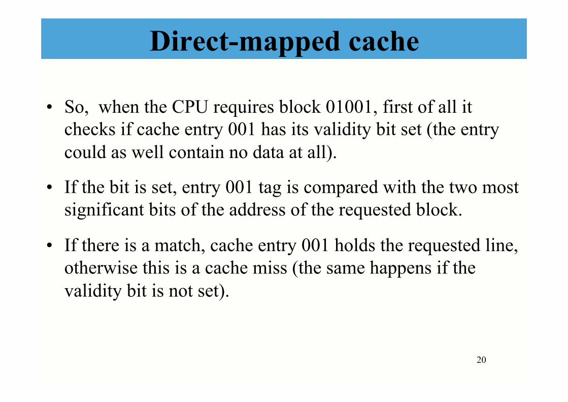
• So, when the CPU requires block 01001, first of all it checks if cache entry 001 has its validity bit set (the entry could as well contain no data at all).
• If the bit is set, entry 001 tag is compared with the two most significant bits of the address of the requested block.
• If there is a match, cache entry 001 holds the requested line, otherwise this is a cache miss (the same happens if the validity bit is not set).
20
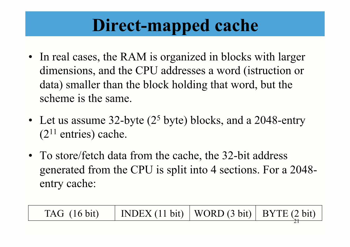
Direct-mapped cache • In real cases, the RAM is organized in blocks with larger
dimensions, and the CPU addresses a word (istruction or data) smaller than the block holding that word, but the scheme is the same.
• Let us assume 32-byte (25 byte) blocks, and a 2048-entry (211 entries) cache.
• To store/fetch data from the cache, the 32-bit address generated from the CPU is split into 4 sections. For a 2048-entry cache:
21 TAG (16 bit) INDEX (11 bit) WORD (3 bit) BYTE (2 bit)

Direct-mapped cache • Where:
– TAG: the 16 most significant bits in the CPU generated address.
– INDEX: the cache entry holding the data item, if present (note: 211=2048)
– WORD: which 4-byte word within the 32-byte block is actually referenced (23 = 8; 8 x 4 = 32)
– BYTE: usually unused, it specifys the byte referenced within the world.
22

Direct-mapped cache • The block whose address in RAM is:
“TAG – INDEX – 0 0 0 0 0”
• contains all RAM bytes from address
“TAG – INDEX – 0 0 0 0 0”
to address
“TAG – INDEX – 1 1 1 1 1”
• Which addresses have the 8 4-byte words stored in line with address “TAG – INDEX – 0 0 0 0 0”?
23
16 bit 11 bit

Direct-mapped cache • When the CPU generates an address, the hardware extracts the 11 bits
for INDEX, and uses them to address one of the 2048 entries in the cache
– Question 1: why are the remaining 5 least significant address bits unused ?
– Question 2: what about the computation: (RAM block address) modulo (Number of cache entries)
• If the corresponding entry is valid (as specified by the validity bit), the TAG field in the cache entry and the TAG address field are compared (the 16 most significant address bits).
• If they are equal, this is a cache hit. Through the WORD field, only the addressed word is extracted from the cache (the same happens with the BYTE field, if a specific byte is addressed). 24
what is the “block address”?

Direct-mapped cache • If the entry is invalid, or the two TAGs do not match, this is
a cache miss.
• The missing block is fetched from RAM and it replaces the one (possibly) present (here is the temporal locality principle: an item used more recently substitutes an older one)
• Obviously, a cache miss always produces a waste in time (slightly) longer than the time required to directly fetch the data from RAM.
• In any case, all this operations are carried out in parallel in hardware, for maximum speed. 25

Direct-mapped cache • A direct-mapped cache with1024 4-byte entries. The 20 most
significant bits are used as a tag, the 10 intermediate ones as block index, the remaining 2 least significant bits for addressing the byte within the block (Patterson-Henessy, fig. 7.7)
26
• Should we address 2-byte words within the blocks, which part of the CPU generated address would we use?

Cache dimension • The “effective” cache dimension is larger than the
“nominal” one: for each block, it is necessary to store the tag block and its validity bit.
• Let us consider for example a 16 Kbyte cache (214 bytes = 16384 bytes) with 1024 entries (210), so 16-byte blocks (24) byte.
• If the address is 32 bits, each tag is composed of 32 – 10 – 4 = 18 bits, plus the validity bit, so that each entry has 128 + 19 = 147 bits.
• Overall, the cache stores 1024 · 147 = 150528 bits, that is 18816 bytes.
27

Block dimension
• Cache performances depend also on block dimension. Generally speaking, larger blocks allow to reduce cache misses, because they exploit better spatial locality.
• However, block dimension cannot be enlarged beyond a certain level, because, for a given cache capacity, the larger the block size, the smaller the number of blocks in the cache, so the higher the probability to substitute a block (cache miss) before all of its data are actually used.
28

Block dimension • The picture (Patterson-Hennessy, 7.8) depicts cache miss frequency vs
block size and cache size in SPEC92 benchmark. Larger caches allow to use larger blocks (and still cause a smaller number of cache misses).
29

Cache miss management • Causes for misses:
– Compulsory misses
• first reference to a block
– Capacity • A block is discarded and later retrieved
– Conflict • A program references multiple addresses that map to the same block in the
cache
30

Cache miss management • What happens in case of cache miss? The pipeline must be
stalled, until the missing instruction or data item is fetched from RAM.
• In case of miss in the I-cache, the current PC must be decremented by the same amount by which it was increased during the IF phase.
• When the block containing the missing instruction/data item has been loaded, execution proceeds. With a missing instruction, the IF phase is executed, with a missing data item, the MEM one.
31

Write policy • Handling writes is more complex, since data must be changed in
RAM as well, sooner or later.
• When a cache block receives a write, a first option is to propagate immediately the change to the RAM, thus maintaining cache coherence.
• In order to maintain cache coherence, with a cache miss on write the missing data item is fetched from RAM, modified in the cache, and written back to RAM.
• This write policy is called write-through: writes are always performed both in the cache and in RAM, so that the data present in both memories are always consistent.
32
Write policy • Write-through exhibits poor performance, since it requires
access to RAM for every write in the cache, an operation that takes a lot of clock cycles.
• A solution to this problem is using a write buffer: a small memory in the CPU that hosts a data item, until it is written to RAM.
• Once the CPU has written in the cache and in the write buffer, it goes on executing, and the write buffer takes care of forwarding the data to RAM. The buffer is released when the write operation is complete.
33

Write policy
• In true architectures, the write buffer holds more entries, to serve multiple frequent write requests: when the buffer gets filled (all data it holds still have to be moved to RAM), the pipeline must be stalled (unless the processor uses dynamic scheduling of the pipeline).
34
Write policy
• An alternative scheme is write-back, which only modifies data in the cache (it is sometimes called write deferred).
• The write is forwarded to RAM (or to lower cache levels, if the are multiple cache levels) only if the data item has to be replaced with another data item having the same tag.
• Write-back requires more data to be stored at each cache block: besides the validity bit, it is necessary to use a dirty bit, which, if set, signals that the block has been modified.
35

Write policy
• Write-back requires a policy to synchronize the cache with lower levels of the hierarchy and RAM in the end.
• A block with dirty bit set is written back in the rest of the hierarchy only when the block must be replaced.
36

Write policy
• Write allocate : the block is allocated first (brought to the cache) then it undergoes one of the write actions .
• No-write allocate : the cache is not affected and the block is written only in lower-level memory hierarchy. The updated block comes to cache only in a subsequent read reference.
• Usually write-back is paired with write allocate, while write-through obviously favors no-write allocate
37

RAM support
• The time required to fetch the data from RAM in case of a miss is called miss penalty.
• The length of miss penalty is due to the three operations necessary to handle a cache miss:
1. Sending to RAM the address of the missing block
2. Accessing the RAM to fetch the block
3. Transmitting the block to the CPU
We disregard the cost of forwarding the block to the cache once it is within the CPU. 38

RAM support
• The first and the third operation can take a single clock cycle (of the bus clock, not the CPU’s), while the second takes much longer, in the order of 10 to 20 clock cycles (of the bus, of course).
• Furthermore, a cache block is usually much larger than the amount of data that a memory bank can output with a single access.
• For instance, a block can have 16 bytes, while a RAM access allows to read a 32-bit word, that is 4 bytes, thus requiring 4 accesses to fetch a whole cache block.
39

RAM support • Let us consider a 32-bit system (with a 32-bit bus).
Supposing that a RAM access takes 15 clock cycles (a reasonable assumption) to read a 32-bit word, to carry out a cache miss for a 16-byte block requires:
– 1 clock cycle to send the missing block address to the RAM
– 4 × 15 clock cycles to read the whole block
– 4 × 1 clock cycle to transmit the whole block to the cache
• This gives a total of 65 clock cycles (bus clock cycles !).
40

RAM support • Improvements can be obtained by:
– increasing the bandwith to the RAM, the amount of data that can be fetched from RAM in a single access (for instance, by having a whole block fetched in a single access).
– widening the bus, so that the whole block extracted from RAM is transmitted to the processor in a single bus clock cycle.
• Widening the bus up to 16×8 bits in parallel is a very costly and difficult approach. All in all, even the increase in RAM bandwith can alone yield considerable advantages.
41

RAM support • To increas RAM bandwith, it is necessary to set up the
RAM with more banks, so that multiple words (not just a single one) can be read or written in a single clock cycle.
• Each bank gives access to a single word of a given block, and to read the (4, in our example) words in parallel, it suffices to send in parallel to each bank the address of block address they belong to.
• This scheme is called interleaved memory and allows to spare on the time required to fetch a whole block from RAM.
42

RAM support • Hennessy-Patterson, Fig
5.27: interlaced memory (c)allows to keep a manageable bus width and to speed up RAM access in cache miss.
43
• On the same case just considered, with approach (c) we get:
• 1 clock cycle to send the missing block address, 15 clock cycles to get the 4 words of the block (the 4 banks are accessed in parallel), 4 × 1 clock cycles to transmit the whole to the cache, with a grand total of 20 clock cycles, against 65 for case (a)

RAM support
44
• Miss penalty Tmiss
• Taddr time to send the ADDRESS of the block
• Tact time to activate a memory row
• Ttrans time to transmit a memory word over the bus
• Given the length of a cache block and the structure of the memory, it is sufficient to estabilish the number of activations Nact and the number of transfers Ntrans, so that the miss penalty is:
• Tmiss=Taddr + Nact x Tact+ Ntrans x Ttrans
• This figure is usually expressed in number of EXTERNAL BUS clock cycles and then can be mapped to PROCESSOR’s clock cycles
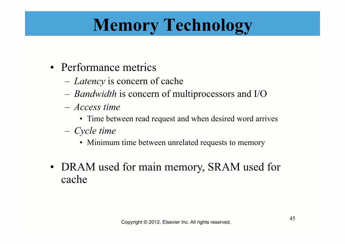
Memory Technology
45
• Performance metrics – Latency is concern of cache – Bandwidth is concern of multiprocessors and I/O – Access time
• Time between read request and when desired word arrives – Cycle time
• Minimum time between unrelated requests to memory
• DRAM used for main memory, SRAM used for cache
Copyright © 2012, Elsevier Inc. All rights reserved.

Memory Technology
46 Copyright © 2012, Elsevier Inc. All rights reserved.
• SRAM – Requires low power to retain bit – Requires 6 transistors/bit
• DRAM – Must be re-written after being read – Must also be periodically refreshed
• Every ~ 8 ms • Each row can be refreshed simultaneously
– One transistor/bit – Address lines are multiplexed:
• Upper half of address: row access strobe (RAS) • Lower half of address: column access strobe (CAS)

Memory Technology
47 Copyright © 2012, Elsevier Inc. All rights reserved.
• Amdahl: – Memory capacity should grow linearly with processor
speed – Unfortunately, memory capacity and speed has not kept
pace with processors
• Some optimizations: – Multiple accesses to same row – Synchronous DRAM
• Added clock to DRAM interface • Burst mode with critical word first
– Wider interfaces – Double data rate (DDR) – Multiple banks on each DRAM device

Memory Technology
48 Copyright © 2012, Elsevier Inc. All rights reserved.
HP5- Fig. 2.12 Internal organization of a DRAM. Modern DRAMs are organized in banks, typically four for DDR3. Each bank consists of a series of rows. Sending a PRE (precharge) command opens or closes a bank. A row address RAS is sent with an Act (activate), which causes the row to transfer to a buffer. When the row is in the buffer, it can be transferred by successive column addresses CAS at whatever the width of the DRAM is (typically 4, 8, or 16 bits in DDR3) or by specifying a block transfer and the starting address. Each command, as well as block transfers, are synchronized with a clock.

Memory Technology
49 Copyright © 2012, Elsevier Inc. All rights reserved.
HP5 - Figure 2.31 DDR2 SDRAM timing diagram.

Memory Technology
50 Copyright © 2012, Elsevier Inc. All rights reserved.

Memory Technology
51 Copyright © 2012, Elsevier Inc. All rights reserved.
Memory Technology
52 Copyright © 2012, Elsevier Inc. All rights reserved.
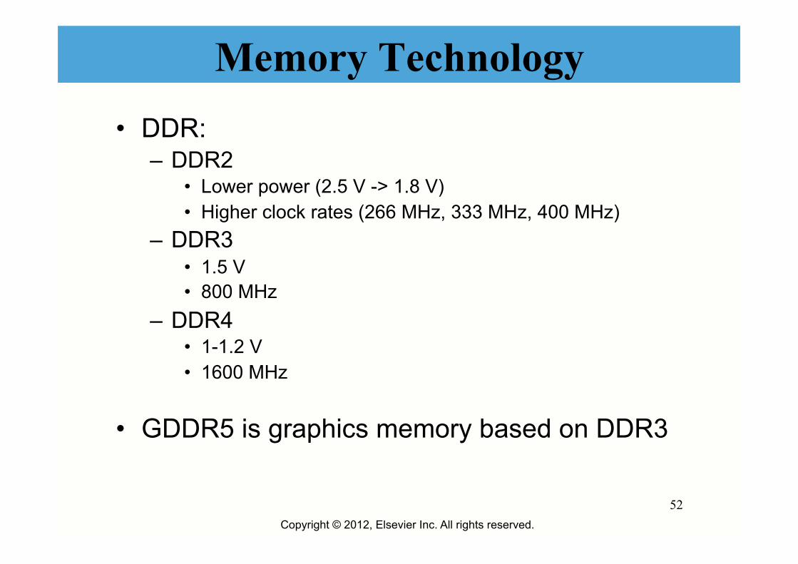
• DDR: – DDR2
• Lower power (2.5 V -> 1.8 V) • Higher clock rates (266 MHz, 333 MHz, 400 MHz)
– DDR3 • 1.5 V • 800 MHz
– DDR4 • 1-1.2 V • 1600 MHz
• GDDR5 is graphics memory based on DDR3

Memory Technology
53 Copyright © 2012, Elsevier Inc. All rights reserved.
HP5 - Figure 2.15 Power consumption for a 2 Gb DDR3 SDRAM operating under three conditions: low power (shutdown) mode, typical system mode (DRAM is active 30% of the time for reads and 15% for writes), and fully active mode, where the DRAM is continuously reading or writing when not in precharge. Reads and writes assume bursts of 8 transfers. These data are based on a Micron 1.5V 2Gb DDR3-1066.

Set-Associative caches • A basic feature of direct-mapped caches is that a RAM
block is always stored in the same cache entry.
• So, multiple RAM blocks match the same cache entry, since the cache is much smaller than the RAM.
• Allowing a more flexible block placement in the cache, it is possible to reduce cache misses, thus increasing system performance.
• This result can be obtained with n-way set-associative caches, where n is usually 2, 4 or 8.
54
Set-Associative caches
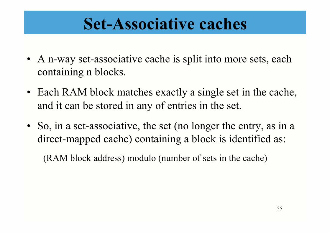
• A n-way set-associative cache is split into more sets, each containing n blocks.
• Each RAM block matches exactly a single set in the cache, and it can be stored in any of entries in the set.
• So, in a set-associative, the set (no longer the entry, as in a direct-mapped cache) containing a block is identified as:
(RAM block address) modulo (number of sets in the cache)
55

Set-Associative caches • A direct mapped cache and a 2-way set-associative cache,
both with a capacity of 8 blocks. In the first, block 12 can be placed only in entry number 4. In the second, the same block can be placed either in entry 0 or in entry 1, the are part of set “zero” (Hennessy-Patterson, Fig. 5.4)
56
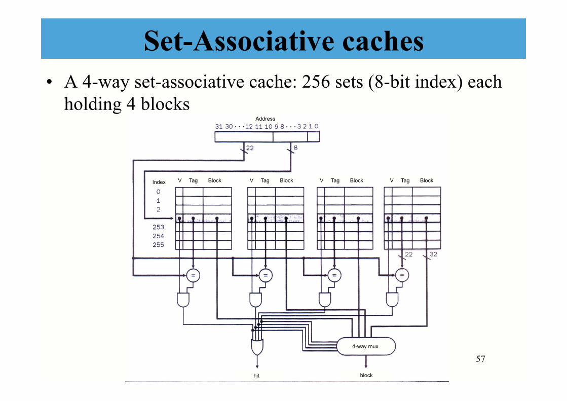
Set-Associative caches • A 4-way set-associative cache: 256 sets (8-bit index) each
holding 4 blocks
57
Address
Index V Tag Block V Tag Block V Tag Block V Tag Block
4-way mux
block hit

Set-Associative caches • Once identified the set containing a given block, it is still
necessary to locate the entry holding the addressed block (through an associative search on all elements in the set).
• If the addressed block is missing, it must be brought into the cache, and if its set is full, one of the blocks of the set must be overwritten. Usually the “victim” block is the least recently used one (LRU block replacement policy).
• The circuitry required for this type of cache is more complex, but performance are better than with direct-mapped caches.
58

Set-Associative caches • As an example, let us consider two caches, each 4-entry, the
first is direct-mapped, the second is 2-way set-associative.
• Let us assume accesses to RAM blocks with addresses 0, 8, 0, 6, 8.
• How many cache misses do result?
59

Set-Associative caches • For the direct-mapped cache, addressed blocks will be placed in the
following cache entries:
Block address Cache entry nella cache 0 0 modulo 4 = 0 6 6 modulo 4 = 2 8 8 modulo 4 = 0
60
• References “0, 8, 0, 6, 8” cause 5 cache misses, since blocks 0 and 8 alternate within the same entry, and the first reference to any block causes a miss, obviously.
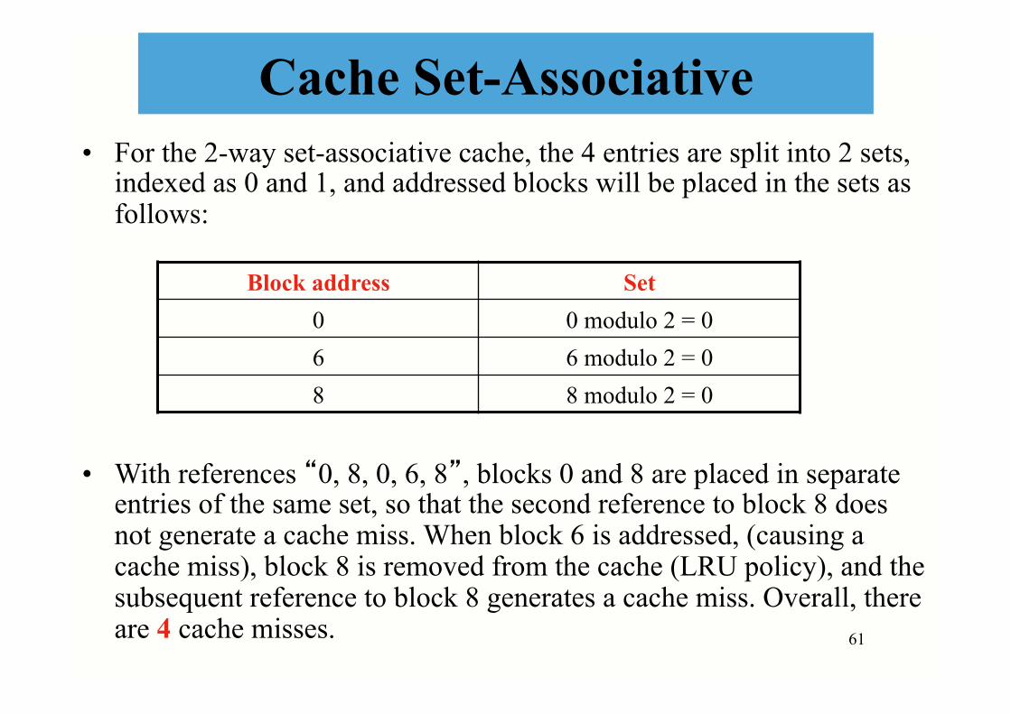
Cache Set-Associative • For the 2-way set-associative cache, the 4 entries are split into 2 sets,
indexed as 0 and 1, and addressed blocks will be placed in the sets as follows:
Block address Set 0 0 modulo 2 = 0 6 6 modulo 2 = 0 8 8 modulo 2 = 0
61
• With references “0, 8, 0, 6, 8”, blocks 0 and 8 are placed in separate entries of the same set, so that the second reference to block 8 does not generate a cache miss. When block 6 is addressed, (causing a cache miss), block 8 is removed from the cache (LRU policy), and the subsequent reference to block 8 generates a cache miss. Overall, there are 4 cache misses.

Set-Associative caches • If the set-associative cache were 4-way, one can easily check that the
previous sequence would result in 3 cache misses.
• By extension, an associative cache with a single, large set, where a block can be placed in any entry, is called fully associative cache.
• This type of cache yields best performance as to cache misses, but caches with (a few) thousands entries are much too complex and expensive to build.
• Still, the principle is valid: the larger the number of entries available for placing blocks (that is, the larger n, the number of ways), the better the performances.
62

Set-Associative caches
• Miss rate in a D-cache for different types of caches with the same capacity (using SPEC2000 as benchmark) (Patterson-Hennessy, fig. 7.15)
Associativity Miss rate 1-way (direct mapped) 10.3%
2-way 8.6%
4-way 8.3% 8-way 8.1%
63
• The advantages with different associativity seem minimal, but they are not, considering the cost of serving even a single miss…

Performances: a simple example
• What is the effect of the cache subsystem on CPU performance ? Let us make a simple estimate (with reasonable values):
– instruction execution time (CPI): 1 clock cycle
– average miss rate: 2%
– average memory reference per instruction: 1,5
– time to fetch a data item from memory in case of miss: 100 clock cycles (CPU)
64

Performances: a simple example
• What is the CPI, assuming a “perfect” cache? (cache miss = 0, access time = 0). Answer = 1 CPI
• What would be the CPI, with no cache at all?
– CPI = 1 + 100 × 1,5 = 151
• And with a “real” cache?
– CPI = 1 × 0,98 + 0,02 × 100 × 1,5 = 4 (yet, assuming a cache with 0 acces time)
65
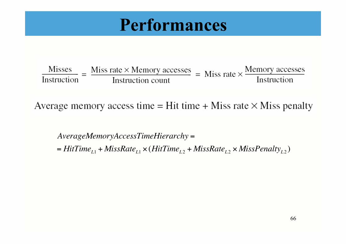
Performances
66
AverageMemoryAccessTimeHierarchy == HitTimeL1 +MissRateL1 × (HitTimeL2 +MissRateL2 ×MissPenaltyL2 )

Increase in performance
• A cache has better effects on system performances :
1. the smaller (in time) the hit time
2. the smaller (in time) the cost of a miss
3. the smaller the miss rate
67

Reducing the cost of a cache miss
• The performance gap between RAM and CPU widens in time, so the cost of a miss gets higher and higher.
• Memory interleaving is a technique to reduce the time required to fetch from RAM a missing block.
• Another way to reduce cache miss cost consists of using multiple levels of cache, to avoid going down to main memory to get the missing block.
• With this approach, it is possible to find a reasonable trade-off between the requirements of having a cache running at the same speed as the CPU (expensive, and so small), and a cache large enough to hold a sufficient fraction of RAM (slower, but less expensive)
68
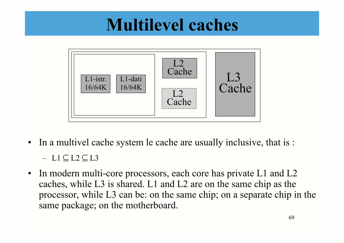
Multilevel caches
• In a multivel cache system le cache are usually inclusive, that is : – L1 ⊆ L2 ⊆ L3
• In modern multi-core processors, each core has private L1 and L2 caches, while L3 is shared. L1 and L2 are on the same chip as the processor, while L3 can be: on the same chip; on a separate chip in the same package; on the motherboard.
69
L1-istr. 16/64K
L1-dati 16/64K
L2 Cache
L3
Cache
L2 Cache

Multilevel caches
• In a system with at least two cache levels, the following should be true:
1. first level caches have an access time close to or equal to CPU speed, thus causing no delay in case of cache hit.
2. the second level cache is sufficiently larger than first level ones, so that the number of second level misses is considerably smaller than first level misses.
3. the third level cache has the same relationship with the second level one.
70
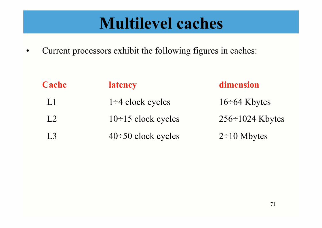
Multilevel caches • Current processors exhibit the following figures in caches:
Cache latency dimension
L1 1÷4 clock cycles 16÷64 Kbytes
L2 10÷15 clock cycles 256÷1024 Kbytes
L3 40÷50 clock cycles 2÷10 Mbytes
71

Multilevel caches • The three-level cache hierarchy of Intel i7:
Cache access time associtivity dimension
L1 D-cache 4 cycles 8-way 32 Kbytes
L1 I-cache 4 cycles 4-way 32 Kbytes
L2 10 cycles 8-way 256 Kbytes
L3 35 cycles 16-way 2 Mbytes per core
72

Reducing cache misses
• It is the second best way to improve cache efficiency. There are multiple options:
– First of all, set-associativity lowers cache miss rate.
– A proper block dimension (with respect to cache capacity) optimizes cache misses for a given cache dimension.
– Obviously, cache misses are reduced by enlarging the cache.
73

Reducing cache misses
• Cache dimensions (L2 and L3 especially) have increased steadily: in 2001 a L2 cache was as large as the main memory in a desktop system of 1991.
• If the cache is too small at any level with respect to the amount of data/instructions required by a program, there arises a true thrashing effect, similar to what happen with virtual memory (see the notion studied in Operating Systems)
74