Quadrature-Based Moment Methods- High-Order Realizable Schemes An
Upload
darren-mcbrideCategory
view
213download
0
Basic building blocks and architectures for realizable QCA
devices
Michael Niemier
(with contributions from Amitabh Chaudhary, Danny Chen, Pranay Harsh, Sharon Hu, Peter Kogge, Craig Lent, Marya Lieberman, Wolfgang Porod,
Ram Ravichandran, and Kevin Whitton)
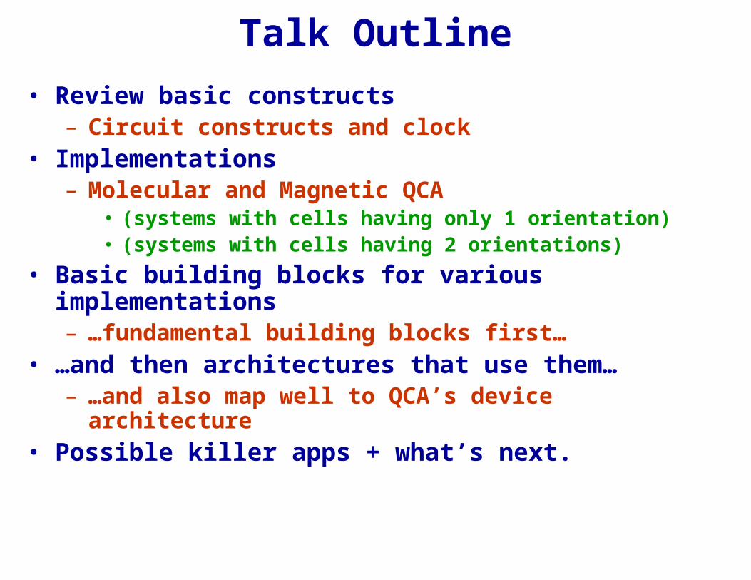
Talk Outline
• Review basic constructs – Circuit constructs and clock
• Implementations– Molecular and Magnetic QCA
• (systems with cells having only 1 orientation)• (systems with cells having 2 orientations)
• Basic building blocks for various implementations– …fundamental building blocks first…
• …and then architectures that use them…– …and also map well to QCA’s device
architecture• Possible killer apps + what’s next.
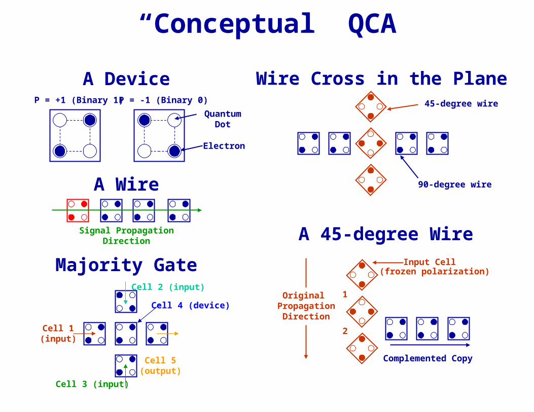
“Conceptual” QCA
Majority Gate
Cell 3 (input)
Cell 2 (input)
Cell 1(input)
Cell 5(output)
Cell 4 (device)
A DeviceP = +1 (Binary 1)P = -1 (Binary 0)
QuantumDot
Electron
Wire Cross in the Plane
90-degree wire
45-degree wire
A 45-degree Wire
Complemented Copy
Input Cell
1
2
(frozen polarization)
Original Propagation
Direction
A Wire
Signal Propagation Direction

Clocked Molecular QCA
No current leads. No need to contact individual molecules.
Active Domain
Null Domain
Switching Region

Can use clock for I/O too…
Permanent 0 here
To “all QCAlogic”
Permanent 1 here
Lithographic pitchLithographi
c pitch
T-Junction
How does a signal from “off chip” address an individual molecular QCA device that is approximately 1.2 nm x 1.2
nm?
Clock wires
“Sticky regions”
10
50 nm
48 nm
T-junction input mapped to 23 tile DNA raft
Need a lithographic clock anyhow - use it to provide paths to permanent 0s and 1s.

Implementations
• Molecular– See Craig Lent’s talk…
• Magnetic– Bigger: 100s of nm (A,B)
– Energy difference b/t 2 states ~ 100-200 kbT (A,B)
• (This is at room tempetature)
• (Energy of 40kbT needed to keep thermally induced errors < 1/year) (A)
– Maximum dot dissipation ~ 10-17 J (A)
• Microprocessor might dissipate ~ 1W (A)
– Slower: ~100s of MHz for cross-chip frequency (A)
– Could be integrated w/MRAM, insensitive to radiation (B)
– Useful for space, military applications?
A: R.P. Cowburn and M.E. Welland, Science, Vol. 287, Issue 5457, 1466-1468, February 2000.
B: G.H. Bernstein et. al., Microelectronics Journal, 36 (2005) p. 619-624.
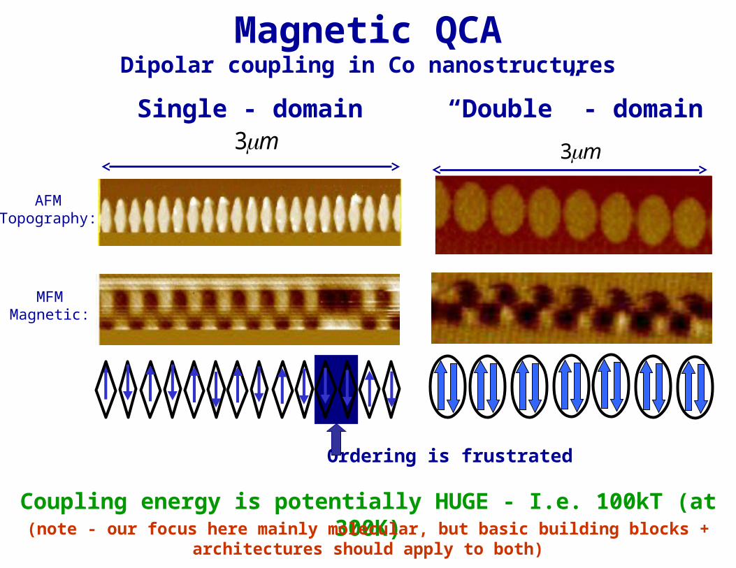
Magnetic QCADipolar coupling in Co nanostructures
Single - domain “Double” - domain
m3m3
AFMTopography:
MFMMagnetic:
Ordering is frustrated
Coupling energy is potentially HUGE - I.e. 100kT (at 300K)(note - our focus here mainly molecular, but basic building blocks +
architectures should apply to both)

Molecular QCA - directed assembly
(not the only way -- but what I’ll talk about…)
--
--
--
--
Current in wire pushes cell charge to active region; turn cells ON
No charge in wire means charge in cells not pushed up to active site; these cells are OFF
EBL etched track ……
…
DNA Raft
Idea: Integrate non-DNA components (devices + interconnect)
(1) Assemble ~100 nm chunks of circuitry
(2) Further
assembly directed by lithography
12 nm
4 nm
(Tiles have 8 accessible major groove sites) Winfree and Seeman, 1998

Experimental Liftoff of APTES/attachment of DNA rafts
SAMs/liftoff Biomolecules
E-beamFrom Marya Lieberman

Cross-section views of rafts on EBL features
DNA rafts
Average cross section
Line section
Line width 110 ± 10 nm
Height 2.7 nm
Si
APTES
2 nm0.7 nm
“Nanometer scale rafts bulit from DNA tiles,” K. Sarveswaran, P. Huber, M. Lieberman, C. Russo, and C.S. Lent; Proceedings of the 2003 3rd IEEE Conference on Nanotechnology, 2003, p.417-20, vol. 2.

Jammin’ on the surface
=0.55 (~4)jammed
=0.91annealed
= “10 x 40 nm”4-tile raft
Voit et al., JPC 97 5212 1992
On APTES~0.40
On SiO2:<0.02
Next: improve interactions between rafts:
(will actually involve CS theory…)
vs.

Molecular Systems - What’s first?
--
--
--
--
………
Directed assembly…:
…but probably only one cell type on DNA raft…
+ =
This first target is not even that restrictive…
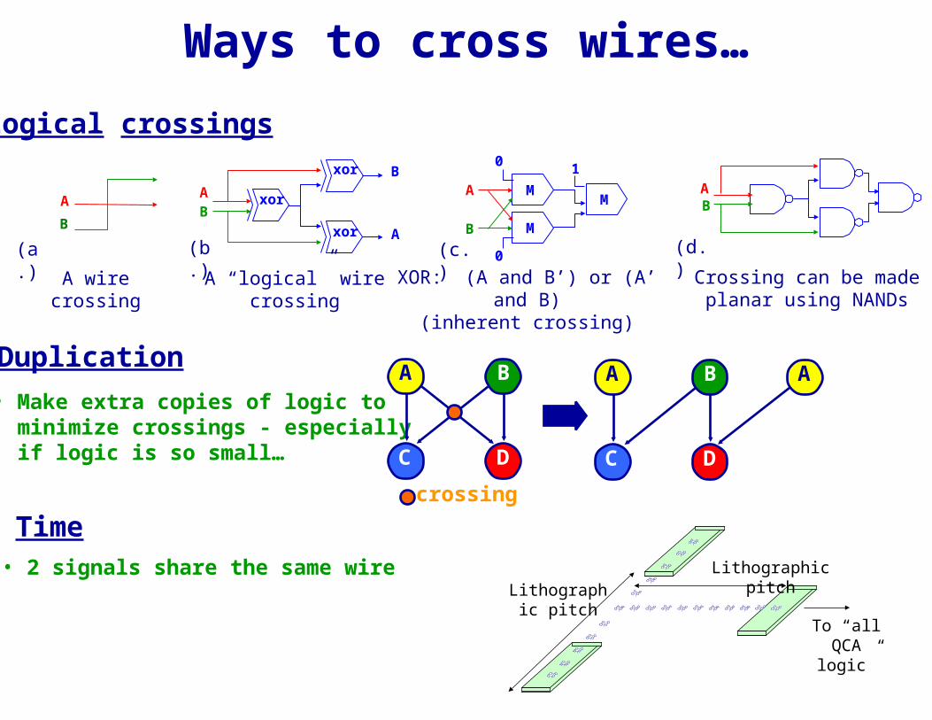
Ways to cross wires…
xor
xor
xor
AB
B
A
A “logical” wire crossing
(b.)
XOR: (A and B’) or (A’ and B)
(inherent crossing)
(c.)
M
M
M
1
A
B
0
0
AB
(d.)
Crossing can be made planar using NANDs
A
B
(a.)
A wire crossing
Logical crossings
Duplication
Time
To “all QCAlogic”
Lithographic pitchLithographi
c pitch
• 2 signals share the same wire
• Make extra copies of logic to minimize crossings - especially if logic is so small…
A
C D
B
crossing
A
C D
B A
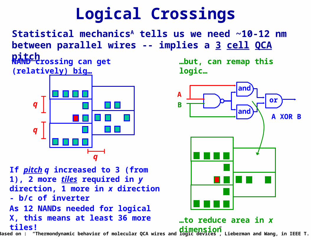
Logical CrossingsStatistical mechanicsA tells us we need ~10-12 nm between parallel wires -- implies a 3 cell QCA pitch
NAND crossing can get (relatively) big…
q
q
q
If pitch q increased to 3 (from 1), 2 more tiles required in y direction, 1 more in x direction - b/c of inverterAs 12 NANDs needed for logical X, this means at least 36 more tiles!
…but, can remap this logic…
A
B
A XOR B
and
and
or
…to reduce area in x dimension
A: Based on : “Thermondynamic behavior of molecular QCA wires and logic devices”, Lieberman and Wang, in IEEE T. Nano.
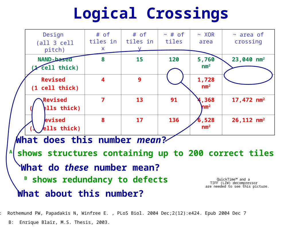
Logical CrossingsDesign
(all 3 cell pitch)# of tiles
in x# of tiles
in y~ # of tiles
~ XOR area
~ area of crossing
NAND-based(1 cell thick)
8 15 120 5,760 nm2
23,040 nm2
Revised (1 cell thick)
4 9 36 1,728 nm2
6,192 nm2
Revised(2 cells thick)
7 13 91 4,368 nm2
17,472 nm2
Revised (3 cells thick)
8 17 136 6,528 nm2
26,112 nm2
A: Rothemund PW, Papadakis N, Winfree E. , PLoS Biol. 2004 Dec;2(12):e424. Epub 2004 Dec 7
A shows structures containing up to 200 correct tiles
What does this number mean?
B: Enrique Blair, M.S. Thesis, 2003.
B shows redundancy to defects QuickTime™ and aTIFF (LZW) decompressor
are needed to see this picture.
What do these number mean?
What about this number?

Area of a "wire crossing"
1
10
100
1000
10000
100000
65 57 50 45 40 35 32 28 25 22 20 18
Technology Node
Are
a o
f a c
ross
ing
in
nm
^2
CMOS
1 cell thick
2 cells thick
3 cells thick
This construct can be smaller than
physical crossing @ 22 nm node.
Logic crossing
Logical CrossingsSome perspective on logical crossing area: Consider…
XOR gate
vs.
(Realistically, to cross 2 metal1 wires, must account for 3x1 metal1
“pitches”)
A AB
Calculated using metal 1 wiring pitch numbers from 2004 ITRS Interconnect Update.
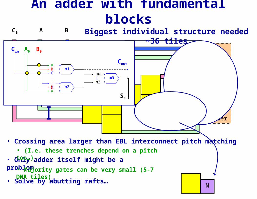
An adder with fundamental blocks
A BCin
Adder
M
M
M
Biggest individual structure needed ~36 tiles
• Crossing area larger than EBL interconnect pitch matching
• Only adder itself might be a problem
m1ABC
m2!CBA
m3!m1Cm2
Cin A0 B0
Cout
S0
• Majority gates can be very small (5-7 DNA tiles)
M• Solve by abutting rafts…
• (I.e. these trenches depend on a pitch too…)

Logic Crossing - basic buildling blocks
A BCin
Adder
M
M
M
John Reif, et. al -- Duke.
Idea: leverage Duke tile for wire… • Can place QCA cells at all points…• …have universal wiring tile…• … simulated with stat. mech.
Goal: tiles self align in EBL trench• “snap together” @ thermal equilibrium

Duplication• Idea: push (some) crosses to inputA
– Also let’s us reuse some basic building/logic blocks
• Duplication… – …works in some cases (all IC local)…
• I.e. in ISCAS benchmark, area decreases as all IC local– …not in others
• Problem inherently can explode exponentially
• Doing this in select cases works…
A: Chaudhary, Chen, Hu, Niemier, Ravichandran, Whitton -- to appear at ICCAD, 2005, San Jose, CA, Nov. 5-9.
Adder
M
M
M
A
B
Cin
B
A
Adder example revisited(Logic small so multiple copies of some blocks
OK…)

Number of devices/cm2 ?
Use previous info./designs for back of envelope calculation: how many QCA devices might be in 1 cm2… Assume:
• Wiring tile (16 cells)
• Reasonable EBL pitch• Parts mapped to DNA
• 3 cell QCA pitch • Some redundancy
Note: Throughput
dependent on granularity of
clock
0 or 10 or 1 0 or 1
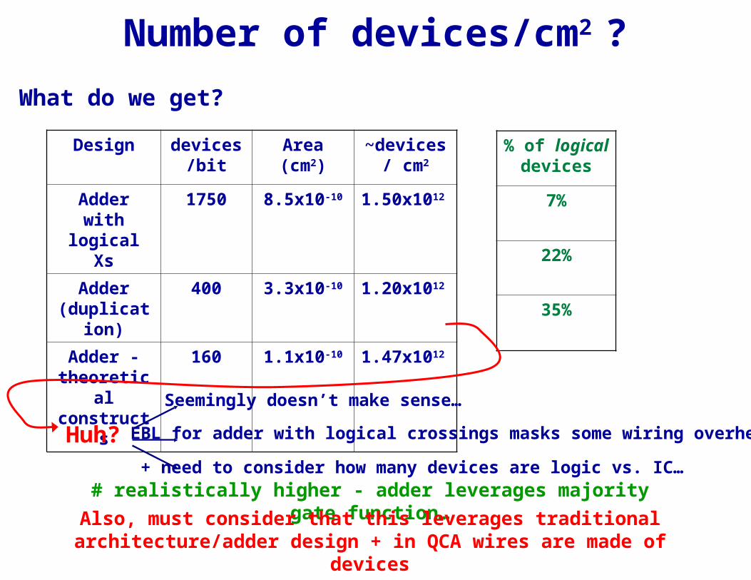
Number of devices/cm2 ?
What do we get?
Design devices/bit
Area (cm2)
~devices/ cm2
Adder with
logical Xs
1750 8.5x10⁻¹⁰ 1.50x101
2
Adder (duplicati
on)
400 3.3x10⁻¹⁰ 1.20x101
2
Adder - theoretica
l construct
s
160 1.1x10⁻¹⁰ 1.47x101
2
% of logical devices
7%
22%
35%
Huh?
Seemingly doesn’t make sense…
+ need to consider how many devices are logic vs. IC…
EBL for adder with logical crossings masks some wiring overhead
# realistically higher - adder leverages majority gate function…Also, must consider that this leverages traditional
architecture/adder design + in QCA wires are made of devices

Architectures• EVERYTHING is pipelined
– In the past, instruction execution was pipelined
– Recently, could say instruction execution needs pipelined wireA
– More recently, global interconnect pipelinedB
– Pipe depth depends in part on granularity of clock wires
B: I.e J. Cong, Y. Fan, Z. Zhang, “Architectural-Level Synthesis for Automatic Interconnect Pipelining”, DAC 2004, June 7-11
A: Hinton, et. al. “The Microarchitecture of the Pentium 4 Processor,” Intel Technology Journal, Q1, 2001, p. 1-12.
ALU
RegMem DM Reg
ALU
RegMem DM Reg
ADD R1, R2, R3
SUB R4, R1, R5
1 2 3 4 5 6 7 8 9 10 11 12 13 14 15 16 17 18 19 20
TC
NX
T IP
TC
Fetc
h
Driv
e
Allo
c
Ren
am
e Ren
am
e Qu
e
Sch
Sch
Sch
Dis
p
Dis
p
RF
RF
Ex
Fig
s
Br C
k
Driv
e
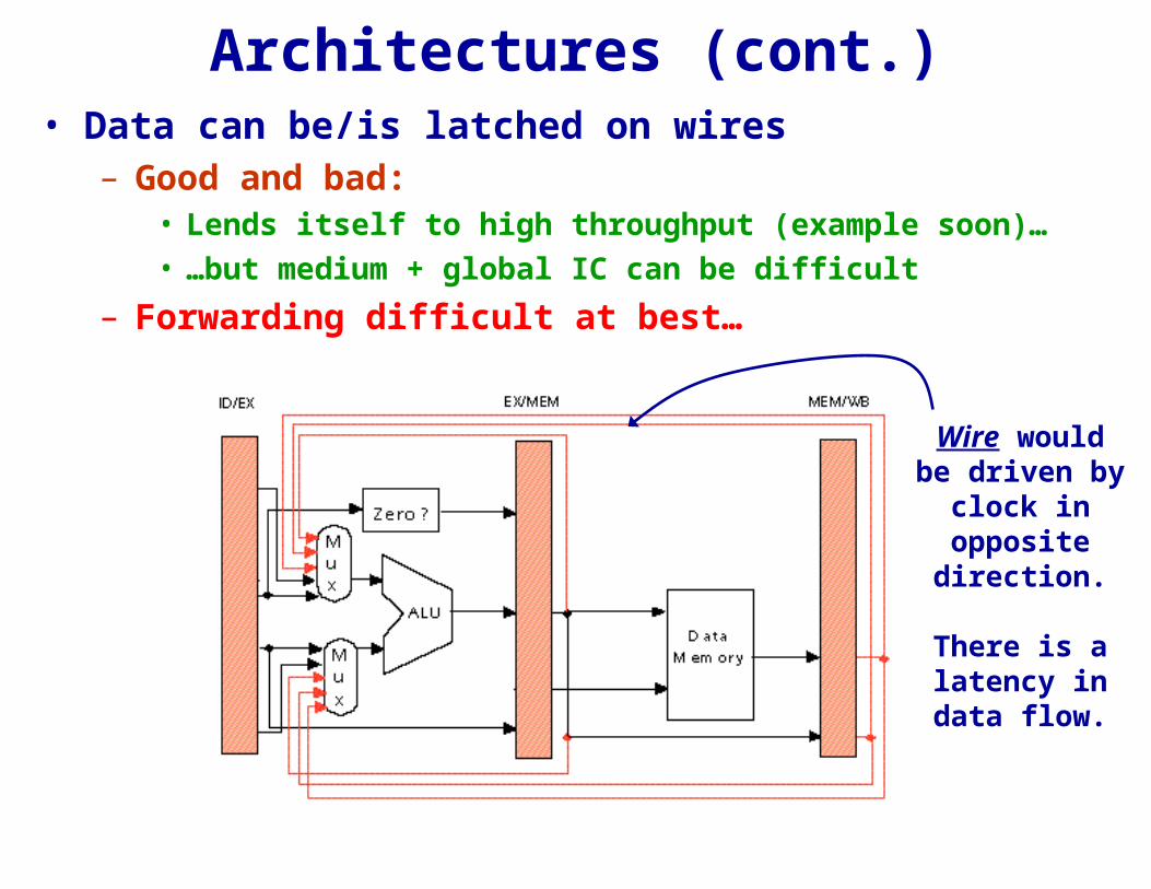
Architectures (cont.)• Data can be/is latched on wires
– Good and bad:• Lends itself to high throughput (example soon)…• …but medium + global IC can be difficult
– Forwarding difficult at best…
Wire would be driven by
clock in opposite direction.
There is a latency in data flow.

Architectures (cont.)
• Defects– Must consider when computing at the nano-
scale…• …especially anything that is self-assembled
– Simple, regular, and replicable offers some protection
• I.e. broken wire or missing tile or defective tile
• We’ll discuss:– PLAs, reconfigurable, systolic, and counterflow
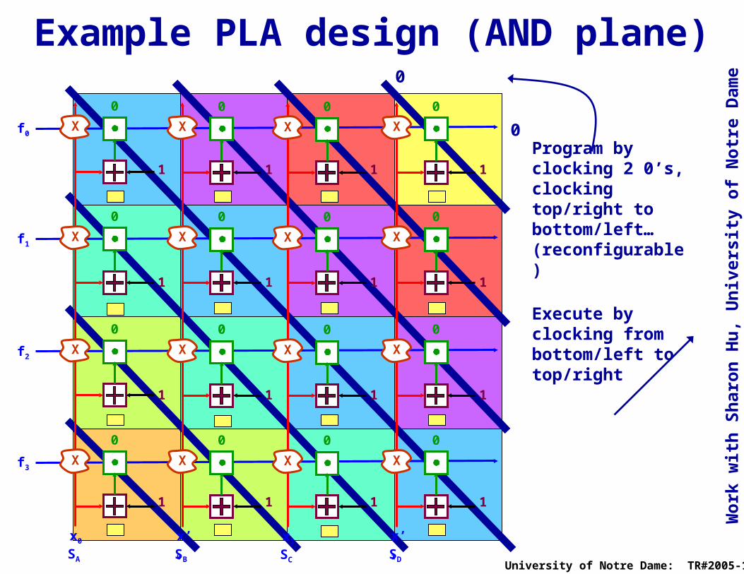
• PLA– again, seemingly “simple” clock + some inherent
redundancy– NOT best architecture for QCA - but illustrates what
might work quite well…
• Systolic and counterflow seem to map well…– …no global IC + potential for simpler clock structures…
• What else?
f0
f1
f2
f3
x0
SA
X
0
1
X
0
X
0
X
0
x’0
SB
X
0
X
0
X
0
X
0
x1
SC
X
0
X
0
X
0
X
0
x’1
SD
X
0
X
0
X
0
X
0
1 1 1
1 1 1 1
1 1 1 1
1 1 1 1
Example PLA design (AND plane)
Work
wit
h S
haro
n H
u,
Un
ivers
ity o
f N
otr
e D
am
e
Program by clocking 2 0’s, clocking top/right to bottom/left…(reconfigurable)
0
0
Execute by clocking from bottom/left to top/right
University of Notre Dame: TR#2005-17
f0
f1
f2
f3
x0
SA
X
0
1
X
0
X
0
X
0
x’0
SB
X
0
X
0
X
0
X
0
x1
SC
X
0
X
0
X
0
X
0
x’1
SD
X
0
X
0
X
0
X
0
1 1 1
1 1 1 1
1 1 1 1
1 1 1 1
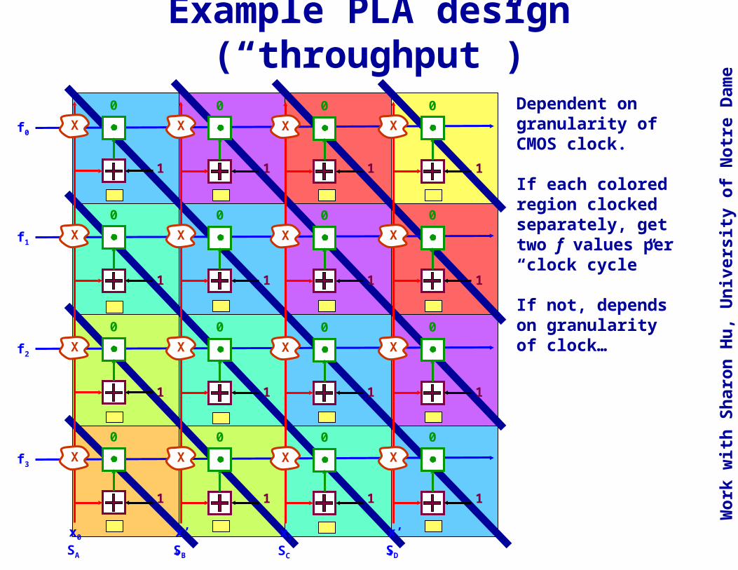
Example PLA design (“throughput”)
Work
wit
h S
haro
n H
u,
Un
ivers
ity o
f N
otr
e D
am
e
Dependent on granularity of CMOS clock.
If each colored region clocked separately, get two f values per “clock cycle”
If not, depends on granularity of clock…

f0
f1
f2
f3
x0
SA
X
0
1
X
0
X
0
X
0
x’0
SB
X
0
X
0
X
0
X
0
x1
SC
X
0
X
0
X
0
X
0
x’1
SD
X
0
X
0
X
0
X
0
1 1 1
1 1 1 1
1 1 1 1
1 1 1 1
Example PLA design (“parts”)
Work
wit
h S
haro
n H
u,
Un
ivers
ity o
f N
otr
e D
am
e
If one cell type, need 1 logical X per node…
(36 tiles/XOR)
AND and OR gates are minimal - 4-6 DNA tiles…
Everything else just wiring tiles…

f0
f1
f2
f3
x0
SA
X
0
1
X
0
X
0
X
0
x’0
SB
X
0
X
0
X
0
X
0
x1
SC
X
0
X
0
X
0
X
0
x’1
SD
X
0
X
0
X
0
X
0
1 1 1
1 1 1 1
1 1 1 1
1 1 1 1
Example PLA design (area)
Work
wit
h S
haro
n H
u,
Un
ivers
ity o
f N
otr
e D
am
e
Back of the envelope calculations…
Considering EBL, each node would be about 150 nm x 150 nm
With all theoretical constructs, each node possibly 110 nm x 60 nm…
0
1
f0
f1
f2
X
0
1
X
0
X
0
X
0
X
0
X
0
X
0
X
0
X
0
1 1
1 1 1
1 1 1
Example PLA design (programming)
Work
wit
h S
haro
n H
u,
Un
ivers
ity o
f N
otr
e D
am
e
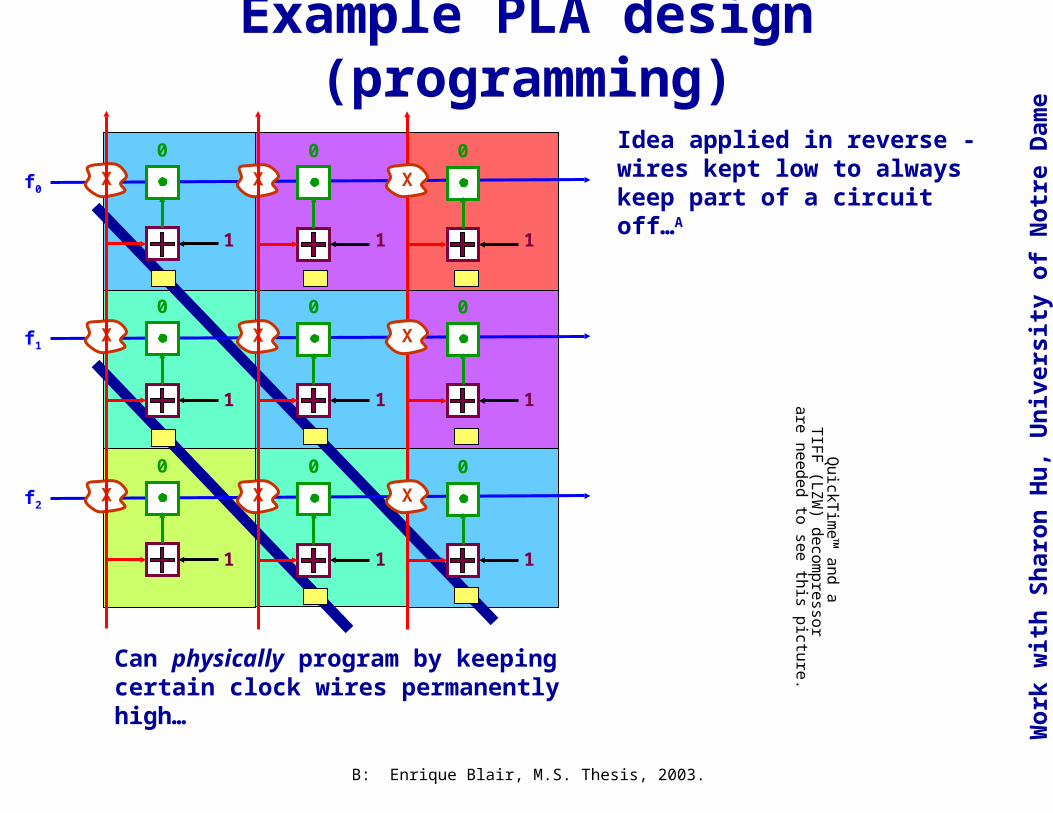
Can physically program by keeping certain clock wires permanently high…
Qu
ickTim
e™
an
d a
TIF
F (L
ZW
) decom
pre
ssor
are
need
ed
to se
e th
is pic
ture
.
Idea applied in reverse - wires kept low to always keep part of a circuit off…A
B: Enrique Blair, M.S. Thesis, 2003.
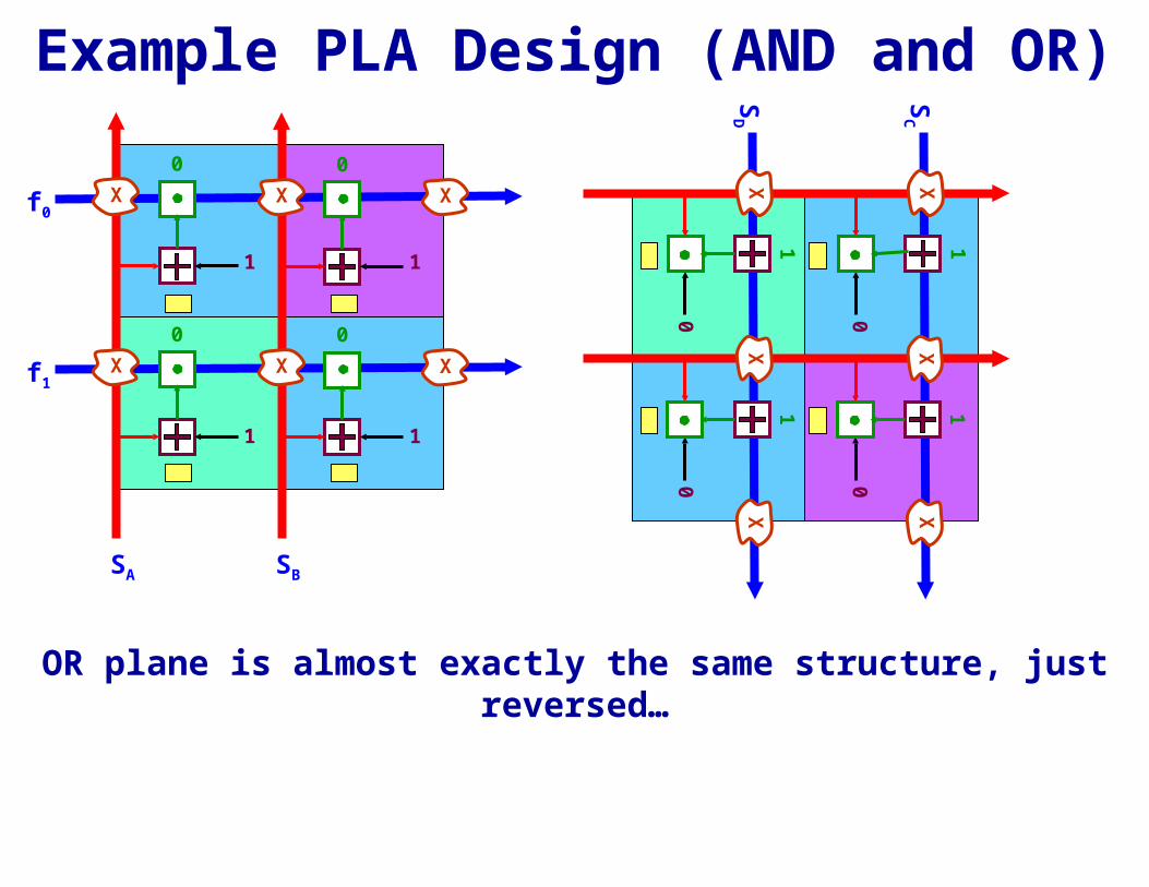
Example PLA Design (AND and OR)
f0
f1
0
1
0
0
0
1
1 1
X
X
X
X
X
X
SA SB
SCSD
1
0
1
11
0
00
XX
XX
XX
OR plane is almost exactly the same structure, just reversed…
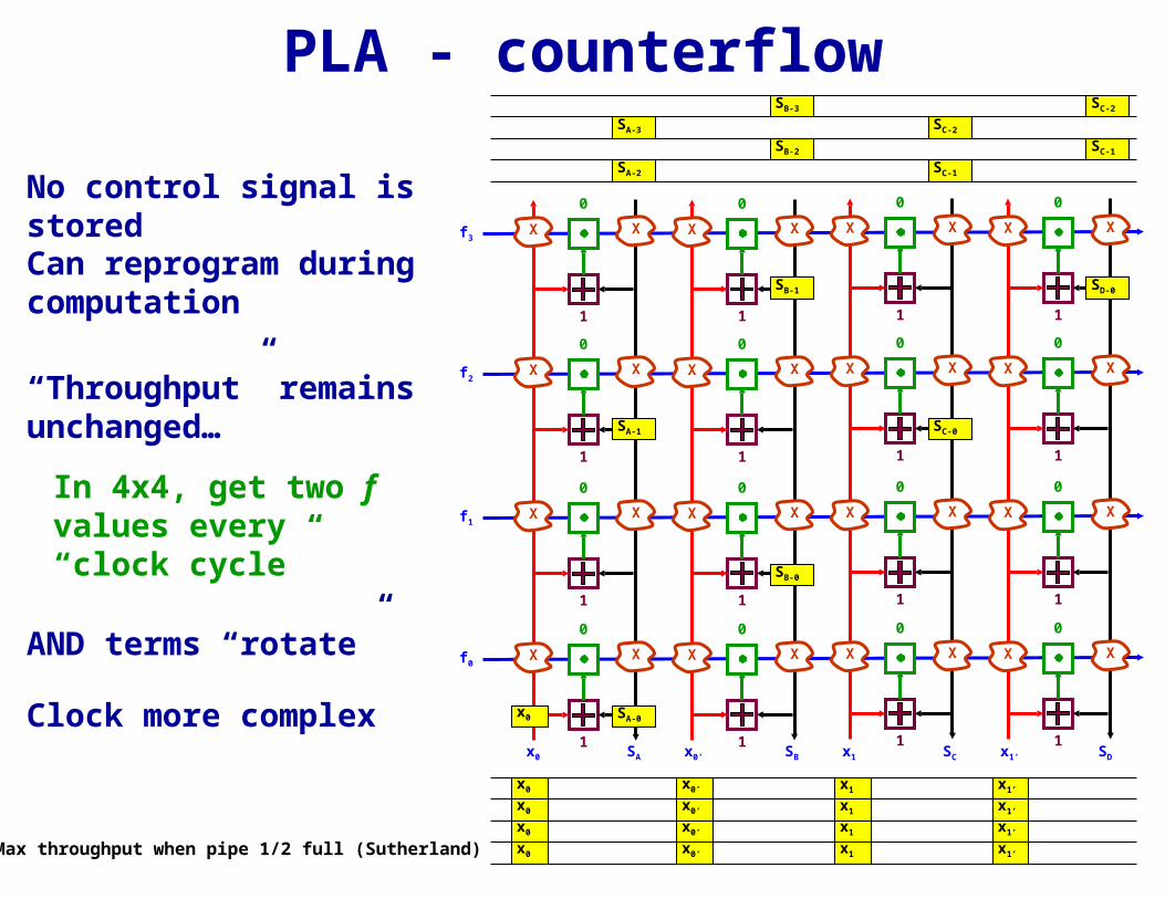
PLA - counterflow
f3X
0
1
X
f2X
0
1
X
f1X
0
1
X
f0X
0
1
X
X
0
1
X
X
0
1
X
X
0
1
X
X
0
1
X
X
0
1
X
X
0
1
X
X
0
1
X
X
0
1
X
X
0
1
X
X
0
1
X
X
0
1
X
X
0
1
X
x0 SA x0’ SB x1 SC x1’ SD
SA-0x0
x0
x0
x0’
x0
x0’
x0
x0’ x1
x1 x1’
SB-0
SC-0
SD-0
SA-1
SB-1
SA-2
SA-3
SB-2
SB-3
SC-1
SC-2
SC-1
SC-2
x0’
x1
x1
x1’
x1’
x1’
No control signal is storedCan reprogram during computation
“Throughput” remains unchanged…
In 4x4, get two f values every “clock cycle”
AND terms “rotate”
Clock more complex
Max throughput when pipe 1/2 full (Sutherland)

Conclusions• Most architectural work should apply to all
implementations– Even with first target, can do interesting things
at reasonable scales…
• Can design a processor + memory to…– Conventional von Neumann architecture
probably not most efficientA…
• CS work should guide PS as to what parts to build 1st…
• Density numbers good for (probably) bad architectures…– …and a gate is only 6 cells and all IC is cells…
A: Niemier, Kogge, ISCA 2001

Conclusions• SystolicA, wave-like, counterflow architectures
all insinuated by PLA slides… (Doug Berger’s work too…)– (Some) applications that might map well to QCA
• Signal processing - FIR, IIR• Matrix arithmetic, Eigenvalue calculations• Non-numeric applications: graph algorithms,
language recognition, polynomial division, etc.
• …interesting designs look possible with even the simplest of constructs…– In working group yesterday…
• Intel successful in part b/c they found a way to build lots of the same basic part with high yield…
• …apply this lesson here…
A: “Why Systolic Architectures,” H.T. Kung, IEEE Comuter, January, 1982, 37-46.


![Project 3 - Graffiti Map - Pranay and Yi-Ying [Updated]](https://static.fdocuments.in/doc/165x107/555afc89d8b42a64398b47a4/project-3-graffiti-map-pranay-and-yi-ying-updated.jpg)


![Swami Narayanananda] the Secrets of Prana, Pranay](https://static.fdocuments.in/doc/165x107/577c82701a28abe054b0c6d6/swami-narayanananda-the-secrets-of-prana-pranay.jpg)