AYOUT ESIGN GUIDE FOR THE X RF ICS 1. Introduction 2 ... · AN685 2 Rev. 0.4 3. Guidelines for...
22
Rev. 0.4 Copyright © 2014 by Silicon Laboratories AN685 AN685 L AYOUT D ESIGN G UIDE FOR THE Si4455/435 X RF IC S 1. Introduction This application note provides guidelines and design examples to help users design PCBs for the next generation EZRadio® RF ICs, such as the Si4455/435x devices, using good design practices that allow for high quality RF performance. The RF performance and the critical maximum peak voltage on the output pin strongly depends on the PCB layout as well as the design of the matching networks. The matching principles are described in detail in “AN693: Si4455 Low Power PA Matching”. Furthermore, these types of RF ICs are also applicable in the RF Stick and RF pico board solutions where a PCB antenna is used, which also requires some considerations in the layout design. For optimal performance, Silicon Labs recommends using the PCB layout design suggestions described in the following sections. 2. Design Recommendations when Using Si4455/435x RF ICs Extensive testing has been completed using reference designs provided by Silicon Labs. It is recommended that designers use the reference designs “as-is” since they minimize de-tuning effects caused by parasitics and generated by component placement and PCB routing. When layouts as shown by the reference designs cannot be followed (as a result of PCB size and shape limitations), then the following layout design rules are recommended. The Si4455 transceiver RF chip uses Class-E TX matching network and a 4-element matching balun on the RX side in Direct Tie configuration (where the TX and RX paths are connected together directly without any additional RF switch). Meanwhile, the Si435x receiver RF chip uses only the 4-element matching balun.
Transcript of AYOUT ESIGN GUIDE FOR THE X RF ICS 1. Introduction 2 ... · AN685 2 Rev. 0.4 3. Guidelines for...

Rev. 0.4 Copyright © 2014 by Silicon Laboratories AN685
AN685
LAYOUT DESIGN GUIDE FOR THE Si4455/435X RF ICS
1. Introduction
This application note provides guidelines and design examples to help users design PCBs for the next generationEZRadio® RF ICs, such as the Si4455/435x devices, using good design practices that allow for high quality RFperformance. The RF performance and the critical maximum peak voltage on the output pin strongly depends onthe PCB layout as well as the design of the matching networks. The matching principles are described in detail in“AN693: Si4455 Low Power PA Matching”. Furthermore, these types of RF ICs are also applicable in the RF Stickand RF pico board solutions where a PCB antenna is used, which also requires some considerations in the layoutdesign. For optimal performance, Silicon Labs recommends using the PCB layout design suggestions described inthe following sections.
2. Design Recommendations when Using Si4455/435x RF ICs
Extensive testing has been completed using reference designs provided by Silicon Labs. It is recommended thatdesigners use the reference designs “as-is” since they minimize de-tuning effects caused by parasitics andgenerated by component placement and PCB routing.
When layouts as shown by the reference designs cannot be followed (as a result of PCB size and shapelimitations), then the following layout design rules are recommended.
The Si4455 transceiver RF chip uses Class-E TX matching network and a 4-element matching balun on the RXside in Direct Tie configuration (where the TX and RX paths are connected together directly without any additionalRF switch). Meanwhile, the Si435x receiver RF chip uses only the 4-element matching balun.
AN685
2 Rev. 0.4
3. Guidelines for Layout Design when Using the Si4455 RF IC
Examples shown in this section are based upon the layout of the 4355-PRXB434M (4355CPRXB434M) picoboard.
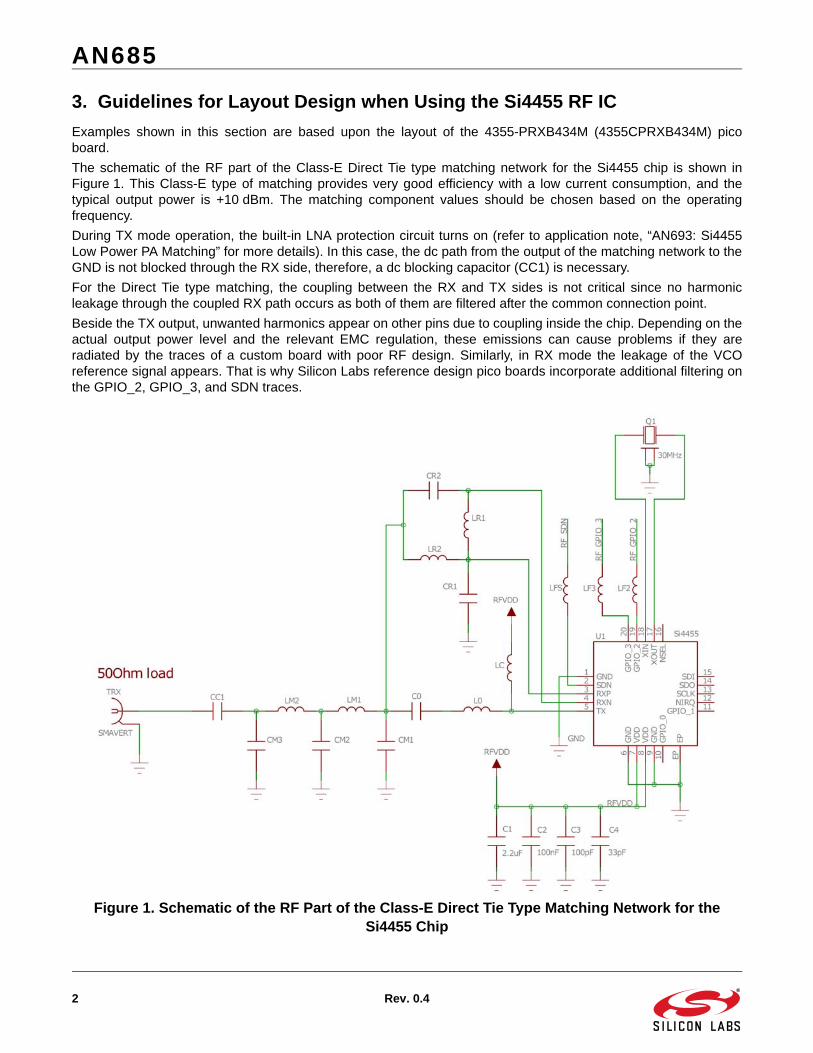
The schematic of the RF part of the Class-E Direct Tie type matching network for the Si4455 chip is shown inFigure 1. This Class-E type of matching provides very good efficiency with a low current consumption, and thetypical output power is +10 dBm. The matching component values should be chosen based on the operatingfrequency.
During TX mode operation, the built-in LNA protection circuit turns on (refer to application note, “AN693: Si4455Low Power PA Matching” for more details). In this case, the dc path from the output of the matching network to theGND is not blocked through the RX side, therefore, a dc blocking capacitor (CC1) is necessary.
For the Direct Tie type matching, the coupling between the RX and TX sides is not critical since no harmonicleakage through the coupled RX path occurs as both of them are filtered after the common connection point.
Beside the TX output, unwanted harmonics appear on other pins due to coupling inside the chip. Depending on theactual output power level and the relevant EMC regulation, these emissions can cause problems if they areradiated by the traces of a custom board with poor RF design. Similarly, in RX mode the leakage of the VCOreference signal appears. That is why Silicon Labs reference design pico boards incorporate additional filtering onthe GPIO_2, GPIO_3, and SDN traces.
Figure 1. Schematic of the RF Part of the Class-E Direct Tie Type Matching Network for the Si4455 Chip

AN685
Rev. 0.4 3
The layout structure of the RF part of the Class-E Direct Tie type matching network is shown in Figure 2.
Figure 2. Layout Structure of the RF Part of the Class-E Direct Tie Type Matching Network for Si4455
3.1. Layout Design Guidelines for Si4455 RF ICSome general rules for designing an RF-related layout for good RF performance:
Use as large continuous ground plane metallization as possible
Avoid the separation of the ground plane metallization
Use as many grounding vias (especially near to the GND pins) as possible to minimize series parasitic inductance between the ground pour and the GND pins
Avoid using long and/or thin transmission lines for connecting the components or else, due to its distributed parasitic inductance, some de-tuning effects can occur
Avoid placing the nearby inductors in the same orientation to reduce the coupling between them
Use tapered line between transmission lines with different width (i.e., different impedance) to reduce the internal reflections
Avoid using loops and long wires to obviate resonances
Ensure good VDD filtering by using bypass capacitors (especially at the range of the operating frequency)
Layout design guidelines for using the Si4455 RF IC:
The choke inductor (LC) should be placed as close to the TX pin of the RF IC as possible (even if this

AN685
4 Rev. 0.4
means the RX is further away) in order to reduce the series parasitic inductance which increases the voltage peak at the internal drain pin.
The trace parasitics are very critical in case of the connection of LR2; therefore, the shortest traces possible should be used for connecting LR2 to the TX side.
The L0 – C0 elements should be placed as close to each other as possible, because these elements are the resonant tank of the Class-E matching which has a very strong effect on the RF performance.
The neighboring matching network components should be placed as close to each other as possible in order to minimize any PCB parasitic capacitance to the ground and the series parasitic inductances between the components.
By connecting CM1 to the GND metal at the other side of the matching network, the suppression of the double-frequency harmonic could increase even by 5 dB by reducing the coupling between stages of the low pass filter.
If space allows, the parallel inductor in the RX path (LR1) should be perpendicular to the nearby inductors in the TX path as this will reduce TX to RX coupling.
Increase the grounding effect in the thermal straps used with capacitors. In addition, thicken the trace near the GND pin of these capacitors. This will minimize series parasitic inductance between the ground pour and the GND pins. Additional vias placed close to the GND pin of capacitors (thus connecting it to the bottom layer GND plane) will further help reduce these effects.
Figure 3 demonstrates the positioning and orientation of the LC, L0, C0, LR1, LR2, and CM1 components on the4355-PRXB434M (4355CPRXB434M) pico board.
Figure 3. Component Orientation and Placement
AN685
Rev. 0.4 5
The smaller VDD bypass capacitors (C4 and C3) should be kept as close to the VDD pins as possible.
The exposed pad footprint for the paddle of the RF IC should use as many vias as possible to ensure good grounding and heatsink capability. In the reference designs there are 9 vias, each with a 12 mil diameter. The paddle ground should also be connected to the top layer GND metal, if possible, to further improve RF grounding; this may be accomplished with diagonal trace connections through the corners of the RFIC footprint.
The crystal should be placed as close to the RFIC as possible to ensure wire parasitic capacitances are kept as low as possible; this will reduce any frequency offsets that may occur.
Use at least 0.5 mm separation between traces/pads to the adjacent GND pour in the areas of the matching networks; this will minimize the parasitic fringe capacitance and reduce the detuning effects.

AN685
6 Rev. 0.4
Figure 4 demonstrates the grounding of the RFIC, the VDD filter capacitors and crystal positions, and the isolationbetween the traces and the ground metal.
Figure 4. RFIC GND Vias and GND Metallization
To achieve good RF ground on the layout, it is recommended to add large, continuous GND metallization on the top layer in the area of the RF section (at a minimum). Better performance may be obtained if this is applied to the entire PCB. To provide a good RF ground, the RF voltage potentials should be equal along the entire GND area as this helps maintain good VDD filtering and also provides a good ground plane for a monopole-type antenna. Gaps ideally should be filled with GND metal and the resulting sections on the top and bottom layers should be connected with as many vias as possible.
The area under the matching network (on the bottom layer) should be filled with ground metal as it will help reduce/remove the unwanted radiated emissions. Board routing and wiring should not be placed in this region to prevent coupling effects with the matching network. It is also recommended that the GND return path between the GND vias of the TX LPF/Match and the GND vias of the RFIC paddle should not be blocked in any way; the return currents should see a clear unhindered pathway through the GND plane to the back of the RFIC.
Use 50 grounded coplanar lines where possible for connecting the SMA connector (or the antenna directly) to the matching network to reduce sensitivity to PCB thickness variation. This method will also reduce unwanted radiations and coupling effects. The interconnections between the elements are not considered to be transmission lines as their lengths are much lower than the wavelength and thus their impedance is not critical. As a result, their recommended width is the smallest possible (i.e., equal to the width of the pad of the applied components). In this way, the parasitic capacitances to the ground can be minimized. For the 4455-PCExxDxxxM (4455CPCExxDxxxM) pico board, the only route where the 50 coplanar transmission line is used is between the output of the matching networks and the SMA connector.

AN685
Rev. 0.4 7
Figure 5 and Figure 6 demonstrates the 50 coplanartransmission line and theGND metal-filled sections on theRF part of the Si4455-LED-434 (Si4455CLED-434) pico board PCB. The top and bottom layers are shown,respectively. Examples for the 50 grounded coplanar trace dimensions are shown in Table 1.
Figure 5. Ground Poured Sections with PCB Vias around the Matching Network—Top Layer
Figure 6. Ground Poured Sections with PCB Vias—Bottom Layer

AN685
8 Rev. 0.4
Figure 7. Grounded Coplanar Line Parameters
Table 1. Parameters for 50 Grounded Coplanar Lines
f 119-960 MHz
T 0.018-0.035 mm
Er 4.6
H 1.5 mm 0.26 m
G 0.25 mm 0.64 mm
W 1.26 mm 0.45 mm
*Note: For the 4-layer PCBs, the thickness between the top and the next inner layer should be taken into account.

AN685
Rev. 0.4 9
Additional concerns for the RF Stick solutions:
The Si4455-LED-xxx (Si4455CLED-xxx) development boards (RFStick solutions) can be optionally broken in two along the connector so that the RF Part can be used as a pico board. Due to this option, the developer must ensure that the ground planes of the RF and MCU sections are connected well as possible to each other. Figure 8 and Figure 9 show this solution for the Si4455-LED-434 (Si4455CLED-434) development board. The top and bottom layers are shown, respectively. As shown in Figure 8 and Figure 9, there are as many connection wires as possible between the two parts to minimize the parasitic inductance in the grounding between the two stages.
Figure 8. Ground Connection between the RF and MCU Parts—Top Layer
Figure 9. Ground Connection between the RF and MCU Parts—Bottom Layer

AN685
10 Rev. 0.4
For optimal RF performance, it is necessary to have a good connection between the two ground plane sections to ensure as large and continuous a ground plane as possible for the monopole-types antennas. This connection will achieve a good antenna characteristic and the best antenna gain.
On the RF Stick there is an option to select between the PCB antenna or the SMA connector (with a 50 SMA antenna)by soldering a 0805 size of 0 resistor to the proper side (see the SMA–PCB ANT selecting 0805 0 in Figure 10).On these boards, the only route where 50 coplanar transmission line is used is between one of the 0805 resistors and the SMA connector since the output of the matching network is very close to the 0805 resistors.
Figure 10 demonstrates the layout structure of the RF part of the Si4455-LED-434 (Si4455CLED-434)development board.
Figure 10. Layout Structure of the RF Part of the 4455-LED-434 (4455CLED-434) Development Board

AN685
Rev. 0.4 11
4. Guidelines for Layout Design when Using the Si435x RF IC
Examples shown in this section are based on the layout of the 4355-PRXB434M (4355CPRXB434M) pico board.
The schematic of the RF part for the Si435x chip is shown in Figure 11. This 4-element matching balun provides asingle-ended to differential conversion that matches the LNA input to a 50 source impedance (i.e., the antenna).In addition, the LR2-CR2 are parallel-resonant at the desired operating frequency. This resonance is an importantfactor in TRX Direct Tie matching because it enables the RF IC to work in TX mode without any output powerdegradation when the RX side shows very high impedance. The matching component values should be chosenbased on the operating frequency.
Figure 11. Schematic of the RF Part for the Si435x Chip
The layout structure of the RF part for the Si435x chip is shown in Figure 12.

AN685
12 Rev. 0.4
Figure 12. RF Layout Structure for the Si4355 Chip
4.1. Layout Design Guidelines for Si435x RF ICThe principles in this case are the same as for the Si4455 boards except for the following issues:
Because only the RX part is applied in this case (no TX matching), the parallel inductor between the differential ports (LR1) should be placed as close to the RX pins of the RF IC as possible to reduce the series parasitic inductance, which may cause de-tuning effects in the matching network.
Since the Si435x-LED-xxx (Si435xCLED-xxx) development boards have the same PCB structure as the Si4455-LED-xxx (Si4455CLED-xxx) development boards, the distance between the RF IC and the SMA connector and the antenna is the same. In addition, a 50 grounded coplanar transmission line is necessary between the SMA-PCB ANT selecting 0805 0 and the matching network to avoid impedance transformation and unwanted radiations by the long trace section.
Figure 13 demonstrates the positioning and orientation of components and grounded coplanar transmission lineson the RF part of the Si4355-LED-434 (Si4355CLED-434) development boards.

AN685
Rev. 0.4 13
Figure 13. Layout of the RF Part of the Si4355-LED-434 (Si4355CLED-434) Development Board

AN685
14 Rev. 0.4
5. PCB Antennas for Si4455/Si435x RF ICs
This document shows the PCB antenna layouts that are used in Si4455/435x applications. More information aboutthese antennas and descriptions of their operation can be found in the application note, “AN686: Antennas for theSi4455/435x RF ICs”.
The Si4455 transceiver and Si435x receiver RF chips use the same PCB antennas, and the parameters for theseantennas depend on the operating frequency. Because the antennas are reciprocal and linear, the same antennacan be used for transmitting and receiving. In all cases, the applied antennas are matched/tuned to have 50 input impedance, thus a matching network is required for use between the RF IC and the antenna.
A typical single-ended IFA antenna applied in the Si4355-PRXB315B (Si4355CPRXB315B) development board isshown in Figure 14. Here the tuning arm of the antenna uses two layer curls to reduce the area occupied by theantenna.
Figure 14. Single-ended IFA used in the Si4355-PRXB315B (Si4355CPRXB315B) Development Board
A typical BIFA (balanced IFA) antenna applied in the Si4455-LED-434 (Si4455CLED-434) development board isshown Figure 15. Here also the tuning arm of the antenna uses two layer curls to reduce the area occupied by theantenna.

AN685
Rev. 0.4 15
Figure 15. Differential BIFA used in 4455-LED-434 (4455CLED-434) Development Boards
The BIFA antenna in Figure 15 with the printed balun transformer has a single-ended 50 input, thus between theantenna and the RF IC a 50 matching network is also required. The printed balun drives a differential BIFA andthe impedance match is done by a differential strip line. Furthermore, it is necessary to keep at least 2 mm spacebetween the entire antenna and the border of the PCB to ensure a reliable antenna input impedance and radiatingcharacteristic.
Silicon Labs has tested the use of this type of BIFA antenna to ensure its performance. For example, the inputimpedance of the BIFA antenna at 868 MHz is shown in Figure 16.

AN685
16 Rev. 0.4
Figure 16. Input impedance of BIFA at 868 MHz
One can observe that the input reflection is about –17 dB, which means very good input impedance to 50 .
The outdoor range between two modules (Si4455-LED-868 (Si4455CLED-868) development boards) was alsounder investigation with the follow parameters:
Delivered power to the antenna is approximately +12 dBm
Radiated power is approximately +5 dBm in EIRP (antenna gain is around –7 dB)
Data rate: 2.4 kbps
2-level FSK modulation, deviation: 30 kHz
The measured range is larger than 1 km (the result is shown in Figure 17).
Figure 17. Range at 868 MHz, 1125 m

AN685
Rev. 0.4 17
6. Guidelines for Layout Design when Using the Si4012 RF IC
Examples shown in this section are based upon the layout of the 4012-PSC10B434 (4012CPSC10B434) picoboards.
The schematic of the RF part for the Si4012 chip is shown in Figure 18. The matching network includes the 4-element matching balun and a 3-element low pass filter (the order of the filter can be changed according to therequired suppression of the standard of the used band). This balun transformer provides the optimal termination forthe PA of the RF IC and the differential to single-ended conversion (since the Si4012 RF IC has a differential PAoutput). As shown in Figure 18, the parallel inductor between the PA output differential pins is separated by twoparts, LM2 and LM4, which should have the same value so that the 2nd harmonic can be effectively suppressedwith a shunt capacitor (CM3). The matching principles are described in detail in application note, "AN727: Si4012Matching Network Guide". The matching component values should be chosen based on the operating frequency.
Figure 18. Schematic of the RF Part for the Si4012 Chip
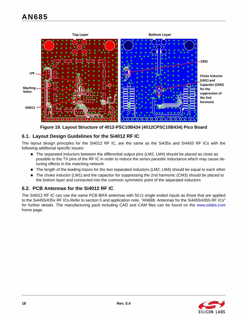
The layout structure of the 4012-PSC10B434 (4012CPSC10B434) pico board is shown in Figure 19.
AN685
18 Rev. 0.4
Figure 19. Layout Structure of 4012-PSC10B434 (4012CPSC10B434) Pico Board
6.1. Layout Design Guidelines for the Si4012 RF ICThe layout design principles for the Si4012 RF IC, are the same as the Si435x and Si4455 RF ICs with thefollowing additional specific issues:
The separated inductors between the differential output pins (LM2, LM4) should be placed as close as possible to the TX pins of the RF IC in order to reduce the series parasitic inductance which may cause de-tuning effects in the matching network
The length of the leading traces for the two separated inductors (LM2, LM4) should be equal to each other
The choke inductor (LM1) and the capacitor for suppressing the 2nd harmonic (CM3) should be placed to the bottom layer and connected into the common symmetric point of the separated inductors
6.2. PCB Antennas for the Si4012 RF ICThe Si4012 RF IC can use the same PCB BIFA antennas with 50 single ended inputs as those that are appliedto the Si4455/435x RF ICs.Refer to section 5 and application note, "AN686: Antennas for the Si4455/4355 RF ICs"for further details. The manufacturing pack including CAD and CAM files can be found on the www.silabs.comhome page.

AN685
Rev. 0.4 19
APPENDIX
This section includes references for all the PCB layouts that use the Si4355 or Si4455 RF IC.
Figure 20. 4455-PCExxDxxxM (4455CPCExxDxxxM) Pico Board
Figure 21. Si4355-LED-434 (Si4355CLED-434) Development Board

AN685
20 Rev. 0.4
Figure 22. Si4355-LED-868 (Si4355CLED-868) & Si4355-LED-915 (Si4355CLED-915) Development Board
Figure 23. Si4355-PRXB434B (4355CPRXB434B) Development Board

AN685
Rev. 0.4 21
DOCUMENT CHANGE LIST
Revision 0.3 to Revision 0.4 4455Cyyy in brackets added to 4455-yyy
4355Cyyy in brackets added to 4355-yyy
4012Cyyy in brackets added to 4012-yyy

DisclaimerSilicon Laboratories intends to provide customers with the latest, accurate, and in-depth documentation of all peripherals and modules available for system and software implementers using or intending to use the Silicon Laboratories products. Characterization data, available modules and peripherals, memory sizes and memory addresses refer to each specific device, and "Typical" parameters provided can and do vary in different applications. Application examples described herein are for illustrative purposes only. Silicon Laboratories reserves the right to make changes without further notice and limitation to product information, specifications, and descriptions herein, and does not give warranties as to the accuracy or completeness of the included information. Silicon Laboratories shall have no liability for the consequences of use of the information supplied herein. This document does not imply or express copyright licenses granted hereunder to design or fabricate any integrated circuits. The products must not be used within any Life Support System without the specific written consent of Silicon Laboratories. A "Life Support System" is any product or system intended to support or sustain life and/or health, which, if it fails, can be reasonably expected to result in significant personal injury or death. Silicon Laboratories products are generally not intended for military applications. Silicon Laboratories products shall under no circumstances be used in weapons of mass destruction including (but not limited to) nuclear, biological or chemical weapons, or missiles capable of delivering such weapons.
Trademark InformationSilicon Laboratories Inc., Silicon Laboratories, Silicon Labs, SiLabs and the Silicon Labs logo, CMEMS®, EFM, EFM32, EFR, Energy Micro, Energy Micro logo and combinations thereof, "the world’s most energy friendly microcontrollers", Ember®, EZLink®, EZMac®, EZRadio®, EZRadioPRO®, DSPLL®, ISOmodem ®, Precision32®, ProSLIC®, SiPHY®, USBXpress® and others are trademarks or registered trademarks of Silicon Laboratories Inc. ARM, CORTEX, Cortex-M3 and THUMB are trademarks or registered trademarks of ARM Holdings. Keil is a registered trademark of ARM Limited. All other products or brand names mentioned herein are trademarks of their respective holders.
http://www.silabs.com
Silicon Laboratories Inc.400 West Cesar ChavezAustin, TX 78701USA
Simplicity StudioOne-click access to MCU tools, documentation, software, source code libraries & more. Available for Windows, Mac and Linux!
www.silabs.com/simplicity
MCU Portfoliowww.silabs.com/mcu
SW/HWwww.silabs.com/simplicity
Qualitywww.silabs.com/quality
Support and Communitycommunity.silabs.com