AVR125 Service Manual
83
harman/kardon AVR125 A/V DOLBY DIGITAL RECEIVER SERVICE MANUAL CONTENTS ESD WARNING………………………….…….2 LEAKAGE TESTING……………….....……....3 BASIC SPECIFICATIONS…………….….…..4 FRONT PANEL CONTROLS………………...5 FRONT PANEL DISPLAY…………………….7 REAR PANEL CONNECTIONS……..….……9 REMOTE CONTROL FUNCTIONS……..…..11 INSTALLATION AND CONNECTIONS….....14 TROUBLESHOOTING GUIDE…………..….16 MICROPROCESSOR RESET……….…..….16 UNIT EXPLODED VIEW………….…..……..17 DISASSEMBLY PROCEDURE..………….18 AMPLIFIER BIAS ADJUSTMENT……...…21 BLOCK DIAGRAM………………………….22 IC PINOUTS……………………………..….23 TRANSISTOR PINOUTS………..…..…….52 ELECTRICAL PARTS LIST………..…..….53 PCB DRAWINGS……………………..……62 SCHEMATICS…………………………...…70 WIRING DIAGRAM..……………………….82 PACKAGING………..…………………...…83 harman/kardon, Inc. 250 Crossways Park Dr. Woodbury, New York 11797 Rev5 2/2005
Transcript of AVR125 Service Manual

harman/kardon
AVR125 A/V DOLBY DIGITAL RECEIVER
SERVICE MANUAL
CONTENTS
ESD WARNING………………………….…….2 LEAKAGE TESTING……………….....……....3 BASIC SPECIFICATIONS…………….….…..4 FRONT PANEL CONTROLS………………...5 FRONT PANEL DISPLAY…………………….7 REAR PANEL CONNECTIONS……..….……9 REMOTE CONTROL FUNCTIONS……..…..11 INSTALLATION AND CONNECTIONS….....14 TROUBLESHOOTING GUIDE…………..….16 MICROPROCESSOR RESET……….…..….16 UNIT EXPLODED VIEW………….…..……..17
DISASSEMBLY PROCEDURE..………….18 AMPLIFIER BIAS ADJUSTMENT……...…21 BLOCK DIAGRAM………………………….22 IC PINOUTS……………………………..….23 TRANSISTOR PINOUTS………..…..…….52 ELECTRICAL PARTS LIST………..…..….53 PCB DRAWINGS……………………..……62 SCHEMATICS…………………………...…70 WIRING DIAGRAM..……………………….82 PACKAGING………..…………………...…83
harman/kardon, Inc.
250 Crossways Park Dr.
Woodbury, New York 11797 Rev5 2/2005

Each precaution in this manual should be followed during servicing.
Components identified with the IEC symbol in the parts list are special significance to safety. When replacing a component identified with
, use only the replacement parts designated, or parts with the same ratings or resistance, wattage, or voltage that are designated in the
parts list in this manual. Leakage-current or resistance measurements must be made to determine that exposed parts are acceptably
insulated from the supply circuit before retuming the product to the customer.
Some semiconductor (solid state) devices can be damaged easily by static electricity. Such components commonly are called
Electrostatically Sensitive (ES) Devices. Examples of typical ES devices are integrated circuits and some field effect transistors and
semiconductor "chip" components.
The following techniques should be used to help reduce the incidence of component damage caused by static electricity.
1. Immediately before handling any semiconductor component or semiconductor-equipped assembly, drain off any electrostatic charge on
your body by touching a known earth ground. Alternatively, obtain and wear a commercially available discharging wrist strap device,
which should be removed for potential shock reasons prior to applying power to the unit under test.
2. After removing an electrical assembly equipped with ES devices, place the assembly on a conductive surface such as aluminum foil, to
prevent electrostatic charge build-up or exposure of the assembly.
3. Use only a grounded-tip soldering iron to solder or unsolder ES devices.
4. Use only an anti-static solder removal device. Some solder removal devices not classified as "anti-static" can generate electrical charges
sufficient to damage ES devices.
5. Do not use freon-propelled chemicals. These can generate electrical change sufficient to damage ES devices.
6. Do not remove a replacement ES device from its protective package until immediately before you are ready to install it. (Most replacement
ES devices are packaged with leads electrically shorted together by conductive foam, aluminum foil or comparable conductive material.)
7. Immediately before removing the protective material from the leads of a replacement ES device, touch the protective material to the
chassis or circuit assembly into which the device will be installed.
Be sure no power is applied to the chassis or circuit, and observe all other safety precautions.
8. Minimize bodily motions when handling unpackaged replacement ES devices. (Otherwise harmless motion such as the brushing together
or your clothes fabric or the lifting of your foot from a carpeted floor can generate static electricity sufficient to damage an ES devices.
CAUTION :
AVR125 harman/kardon

SAFETY PRECAUTIONS
The following check should be performed for the continuedprotection of the customer and service technician.
LEAKAGE CURRENT CHECK
Measure leakage current to a known earth ground (waterpipe, conduit, etc.) by connecting a leakage current testerbetween the earth ground and all exposed metal parts of theappliance (input/output terminals, screwheads, metaloverlays, control shaft, etc.). Plug the AC line cord of theappliance directly into a 120V AC 60Hz outlet and turn theAC power switch on. Any current measured must not exceedo.5mA.
ANY MEASUREMENTS NOT WITHIN THE LIMITSOUTLINED ABOVE ARE INDICATIVE OF APOTENTIAL SHOCK HAZARD AND MUST BECORRECTED BEFORE RETURNING THE APPLIANCETO THE CUSTOMER.
Deviceundertest
Test allexposed metalsurfaces
Also test withplug reversed(Using AC adapterplug as required)
AC Leakage Test
Leakagecurrenttester
Reading shouldnot be above0.5mA
Earthground
3
AVR125 harman/kardon

TECHNICAL SPECIFICATIONS 4
Audio SectionStereo Mode Continuous Average Power (FTC)
55 Watts per channel, @ < 0.07% THD, 20Hz – 20kHz,both channels driven into 8 ohms
Five-Channel Surround Modes Power Per Individual Channel
Front L&R channels:45 Watts per channel@ < 0.07% THD, 20Hz–20kHz into 8 ohms
Center channel:45 Watts @ < 0.07% THD, 20Hz–20kHz into 8 ohms
Surround channels:45 Watts per channel@ < 0.07% THD, 20Hz–20kHz into 8 ohms
Input Sensitivity/ImpedanceLinear (High-Level) 200mV/47k ohms
Signal-to-Noise Ratio (IHF-A) 95dB
Surround System Adjacent Channel SeparationPro Logic II 45dBDolby Digital (AC-3) 55dBDTS 55dB
Frequency Response @ 1W (+0dB, –3dB) 10Hz–100kHz
High Instantaneous Current Capability (HCC) ±25 Amps
Transient Intermodulation Distortion (TIM) Unmeasurable
Slew Rate 40V/µsec
FM Tuner SectionFrequency Range 87.5–108.0MHzUsable Sensitivity IHF 1.3µV/13.2dBfSignal-to-Noise Ratio Mono/Stereo 70dB/68dBDistortion Mono/Stereo 0.2%/0.3%Stereo Separation 40dB @ 1kHzSelectivity ±400kHz, 70dBImage Rejection 80dBIF Rejection 90dB
AM Tuner SectionFrequency Range 520–1710kHzSignal-to-Noise Ratio 45dBUsable Sensitivity Loop 500µVDistortion 1kHz, 50% Mod 0.8%Selectivity ±10kHz, 30dB
Video SectionTelevision Format NTSCInput Level/Impedance 1Vp-p/75 ohmsOutput Level/Impedance 1Vp-p/75 ohmsVideo Frequency Response 10Hz–8MHz (–3dB)
GeneralPower Requirement AC 125V/60HzPower Consumption 68W idle, 540W maximum
(2 channels driven)
Dimensions Width 17.3 inches (440mm)Height 6.6 inches (168mm)Depth 15.4 inches (390mm)
Weight 23.8 lb (10.8kg)
Depth measurement includes knobs, buttons and terminal connections.Height measurement includes feet and chassis.All features and specifications are subject to change without notice.
Harman Kardon is a registered trademark, and Power for the Digital Revolution is a trademark,of Harman Kardon, Inc.
* Manufactured under license from Dolby Laboratories.Dolby, Pro Logic II, AC-3 and the Double-D symbol aretrademarks of Dolby Laboratories. Confidential UnpublishedWorks. ©1992–1999 Dolby Laboratories, Inc. All rights reserved.
DTS and DTS Surround are registered trademarks of Digital Theater Systems, Inc.
UltraStereo is a trademark of UltraStereo Corp.
VMAx is a registered trademark of Harman International Industries, Inc., and is an implementation of Cooper Bauck Transaural Stereo under patent license.
Logic 7 is a registered trademark of Lexicon, Inc., a Harman International Company.
Crystal is a registered trademark of Cirrus Logic Corp.
4
AVR125 harman/kardon

FRONT-PANEL CONTROLS 5
1 Main Power Switch: Press this button to applypower to the AVR 125. When the switch is pressedin, the unit is placed in a Standby mode, as indicatedby the amber LED 3 surrounding the SystemPower Control 2. This button MUST be pressed into operate the unit. To turn the unit off and preventthe use of the remote control, this switch should bepressed until it pops out from the front panel so thatthe word “OFF” may be read at the top of the switch.
NOTE: This switch is normally left in the “ON” position.
2 System Power Control: When the Main PowerSwitch 1 is “ON,” press this button to turn on theAVR 125; press it again to turn the unit off. Note thatthe Power Indicator 3 surrounding the switch willturn green when the unit is on.
3 Power Indicator: This LED will be illuminated inamber when the unit is in the Standby mode to signalthat the unit is ready to be turned on. When the unit is
in operation, the indicator will turn green. Should theindicator turn red, turn the unit off using the MainPower Switch 1 and check the speaker wire con-nections to make certain that there are no short circuits.
4 Headphone Jack: This jack may be used to listento the AVR 125’s output through a pair of headphones.Be certain that the headphones have a standard 1/4"stereo phone plug. The speakers will automatically beturned off when the headphone jack is in use.
5 Selector Buttons: When you are establishing theAVR 125’s configuration settings, use these buttons toselect from the choices available, as shown in the MainInformation Display Û.
6 Tone Mode: Pressing this button enables or dis-ables the Bass and Treble tone controls. When thebutton is pressed so that the words TONE INappear in the Main Information Display Û, the
settings of the Bass & and Treble ( controls maybe used to adjust the output signals. When the buttonis pressed once or twice so that the words TONEOUT appear in the Main Information Display Û,the output signal will be “flat,” without any bass or tre-ble alteration, no matter how the actual Bass andTreble Controls &( are adjusted.
7 Surround Mode Selector: Press this button tochange the surround mode by scrolling through the listof available modes. Depending on the type of input,some modes are not always available. (See page 22for more information about surround modes.)
8 Tuning Selector: Press the left side of the buttonto tune lower-frequency stations and the right side ofthe button to tune higher-frequency stations. When astation with a strong signal is reached, the TUNEDIndicator Q will be illuminated in the MainInformation Display Û .
FRONT-PANEL CONTROLS
1 Main Power Switch2 System Power Control3 Power Indicator4 Headphone Jack5 Selector Buttons6 Tone Mode7 Surround Mode Selector8 Tuning Selector9 AM/FM Selector) Preset Stations Selector
! Input Source Selector@ Tuning Mode Selector# Digital Optical 3 Input$ Digital Coax 3 Input% Video 3 Video Input Jacks^ Video 3 Audio Input Jacks& Bass Control* Balance Control( Treble ControlÓ Volume Control
Ô Set Button Input IndicatorsÒ DelayÚ Digital Input SelectorÛ Main Information DisplayÙ Channel Select Buttonı Speaker Select Buttonˆ Test Tone Selector˜ Surround Mode Indicators¯ Remote Sensor Window
AVR 125
AM/FM
dB
4
Ú
1
3 7
8
9
)
!
@
#
$
%
^
*
&
(
Ó
29 Û Ô
2
6
30
Ò
ˆ
5
Ù
ı
5
AVR125 harman/kardon

6 FRONT-PANEL CONTROLS
FRONT-PANEL CONTROLS
In Manual tuning mode, tap the button lightly and notethat the tuner will step up one frequency increment perbutton press. When the button is held for a few sec-onds you will note that the unit will quickly advancethrough the frequency band. Release it and the tunerwill stop. In Auto tuning mode, each press of the but-ton will search for the next station with an acceptablesignal. Press and hold the button to skip through theacceptable stations. When the button is released, thetuner will not stop until it reaches a station with anacceptable frequency.
To switch back and forth between the Auto andManual tuning modes, press the Tuning ModeSelector @.
9 AM/FM Selector: Pressing this button will auto-matically switch the AVR 125 to the Tuner mode.Pressing it again will switch between the AM and FMfrequency bands. (See page 25 for more informationon the tuner.)
) Preset Stations Selector: Press this button toscroll up or down through the list of stations that havebeen entered into the preset memory. (See page 25for more information on tuner presets.)
! Input Source Selector: Press this button tochange the input by scrolling up or down through thelist of Input Indicators .
@ Tuning Mode Selector: Press this button to selectAuto or Manual tuning. When the button is pressed sothat the AUTO Indicator R lights, the tuner will searchfor the next station with an acceptable signal when theTuning Selector 8u is pressed. When the buttonis pressed so that the AUTO Indicator R is not lit,each press of the Tuning Selector 8u willincrease the frequency. This button may also be used toswitch between Stereo and Mono modes for FM radioreception. When weak reception is encountered, pressthe button until the STEREO Indicator P goes out toswitch to Mono reception. Press and hold again toswitch back to STEREO mode. (See page 25 for moreinformation on using the tuner.)
# Digital Optical 3 Input: Connect the optical digitalaudio output of an audio or video product to this jack.When the input is not in use, be certain to keep theplastic cap installed to avoid dust contamination thatmight degrade future performance.
$ Digital Coax 3 Input: This jack is used for con-nection to the output of portable audio devices, videogame consoles or other products that have a coaxdigital audio jack.
% Video 3 Video Input Jacks: These jacks may beused for temporary connection to the composite or S-Video output of video games, camcorders or otherportable video products.
^ Video 3 Audio Input Jacks: These audio jacksmay be used for temporary connection to videogames or portable audio/video products such as cam-corders and portable audio players.
& Bass Control: Turn this control to modify the low-frequency output of the left/right channels by as much as±10dB, when the unit is in the “Surround Off” mode. Setthis control to a suitable position for your taste or roomacoustics.
* Balance Control: Turn this control to change therelative volume for the front left/right channels.
NOTE: For proper operation of the surround modesthis control should be at the midpoint or “12 o’clock”position.
( Treble Control: Turn this control to modify the highfrequency output of the left/right channels by as much as±10dB, when the unit is in the “Surround Off” mode. Setthis control to a suitable position for your taste or roomacoustics.
Ó Volume Control: Turn this knob clockwise toincrease the volume, counterclockwise to decrease thevolume. If the AVR 125 is muted, adjusting theVolume Control Ó will automatically releasethe unit from the silenced condition.
Ô Set Button: When making choices during thesetup and configuration process, press this button to enter the desired setting as shown in the MainInformation Display Û into the AVR 125’s memory.The set button may also be used to change the displaybrightness. (See page 26.)
Input Indicators: A green LED will light in front ofthe input that is currently being used as the source forthe AVR 125.
Ò Delay: Press this button to begin the sequenceof steps required to enter delay time settings. (Seepage 19 for more information on delay times.)
Ú Digital Input Selector: When playing a sourcethat has a digital output, press this button to selectbetween the Optical #c and Coaxial $·Digital inputs or to select the source’s analog input.(See pages 23–25 for more information on digitalaudio.)
Û Main Information Display: This display deliversmessages and status indications to help you operate
the receiver. (See pages 7–8 for a complete explana-tion of the Information Display.)
Ù Channel Select Button: Press this button tobegin the process of trimming the channel output lev-els using an external audio source. (For more informa-tion on output level trim adjustment, see page 25.)
ı Speaker Select Button: Press this button tobegin the process of configuring the unit to match thetype of speakers used in your listening room. (Seepages 16–19 for more information on speaker setupand configuration.)
ˆ Test Tone Selector: Press this button to beginthe process of adjusting the channel output levelsusing the internal test tone as a reference. (For moreinformation on output level adjustment, see page 18.)
˜ Surround Mode Indicators: A green LED willlight in front of the surround mode that is currently in use.
¯ Remote Sensor Window: The sensor behindthis window receives infrared signals from the remotecontrol. Aim the remote at this area and do not blockor cover it.
33
6
AVR125 harman/kardon
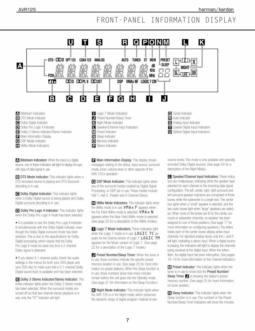
FRONT-PANEL INFORMATION DISPLAY 7
FRONT-PANEL INFORMATION DISPLAY
MEM PRESETSLEEP
AUTOANALOGCOAX 123OPT 123DTS
PCM
TUNED ST
D
D
PL II 3ST DSP VMAx NF LOGIC 7 CM
KHzdB
MHz
NIGHTL RC
SL SRLFE
A
KS RTU Q PO M L
B C D E J
N
F G H I
A Bitstream IndicatorsB DTS Mode IndicatorC Dolby Digital IndicatorD Dolby Pro Logic II IndicatorE Dolby 3 Stereo Indicator/Stereo IndicatorF Main Information DisplayG DSP Mode IndicatorH VMAx Mode Indicators
I Logic 7 Mode IndicatorsJ Preset Number/Sleep TimerK Night Mode IndicatorL Speaker/Channel Input IndicatorsM Preset IndicatorN Sleep IndicatorO Memory IndicatorP Stereo Indicator
Q Tuned IndicatorR Auto IndicatorS Analog Input IndicatorT Coaxial Digital Input IndicatorsU Optical Digital Input Indicators
A Bitstream Indicators: When the input is a digitalsource, one of these indicators will light to display the spe-cific type of data signal in use.
B DTS Mode Indicator: This indicator lights when aDTS-encoded source is playing and DTS Surrounddecoding is in use.
C Dolby Digital Indicator: This indicator lightswhen a Dolby Digital source is being played and DolbyDigital surround decoding is in use.
D Dolby Pro Logic II Indicator: This indicator lightswhen the Dolby Pro Logic II mode has been selected.
• It is possible to see the Dolby Pro Logic II indicatorlit simultaneously with the Dolby Digital indicator, eventhough the Dolby Digital surround mode has beenselected. This is due to the specifications for DolbyDigital processing, which require that the Dolby Pro Logic II mode be used any time a 2-channelDolby signal is detected.
• If you desire 5.1-channel audio, check the audiosettings in the menus for both your DVD player andyour DVD disc to make sure that a 5.1-channel DolbyDigital sound track is available and has been selected.
E Dolby 3 Stereo Indicator/Stereo Indicator: Theentire indicator lights when the Dolby 3 Stereo modehas been selected. When the surround modes areturned off so that two-channel stereo playback is inuse, only the “ST” indicator will light.
F Main Information Display: This display showsmessages relating to the status, input source, surroundmode, tuner, volume level or other aspects of theAVR 125’s operation.
G DSP Mode Indicator: This indicator lights whenany of the surround modes created by Digital SignalProcessing, or DSP are in use. These modes includeHall 1, Hall 2, Theater and 5-Channel Stereo.
H VMAx Mode Indicators: This indicator lights whenthe VMAx mode is in use. VMAx F appears whenthe Far Field VMAx mode is selected; VMAx Nappears when the Near Field VMAx mode is selected.(See page 22 for a description of the VMAx modes.)
I Logic 7 Mode Indicators: These indicators lightwhen the Logic 7 mode is in use. LOGIC 7C ap-pears for the Cinema version of Logic 7; LOGIC 7Mappears for the Music version of Logic 7. (See page22 for a description of the Logic 7 modes.)
J Preset Number/Sleep Timer: When the tuner isin use, these numbers indicate the specific presetmemory location in use. (See page 25 for more infor-mation on preset stations.) When the Sleep function isin use, these numbers show how many minutesremain before the unit goes into the Standby mode.(See page 21 for information on the Sleep Function.)
K Night Mode Indicator: This indicator lights whenthe AVR 125 is in the Night mode, which preservesthe dynamic range of digital program material at low
volume levels. This mode is only available with speciallyencoded Dolby Digital sources. (See page 24 for adescription of the Night Mode.)
L Speaker/Channel Input Indicators: These indica-tors are multipurpose, indicating either the speaker typeselected for each channel or the incoming data-signalconfiguration. The left, center, right, right surround andleft surround speaker indicators are composed of threeboxes, while the subwoofer is a single box. The centerbox lights when a “small” speaker is selected, and thetwo outer boxes light when “large” speakers are select-ed. When none of the boxes are lit for the center, sur-round or subwoofer channels, no speaker has beenassigned to one of those positions. (See page 17 formore information on configuring speakers.) The lettersinside each of the center boxes display active inputchannels. For standard analog inputs, only the L and Rwill light, indicating a stereo input. When a digital sourceis playing, the indicators will light to display the channelsbeing received at the digital input. When the lettersflash, the digital input has been interrupted. (See pages18–19 for more information on the Channel Indicators.)
M Preset Indicator: This indicator lights when thetuner is in use to show that the Preset Number/Sleep Timer J is showing the station’s presetmemory number. (See page 25 for more informationon tuner presets.)
N Sleep Indicator: This indicator lights when theSleep function is in use. The numbers in the PresetNumber/Sleep Timer Indicators will show the minutes
7
AVR125 harman/kardon

8 FRONT-PANEL INFORMATION DISPLAY
FRONT-PANEL INFORMATION DISPLAY
remaining before the AVR 125 goes into the Standbymode. (See page 21 for more information.)
O Memory Indicator: This indicator flashes whenentering presets and other information into the tuner’smemory.
P Stereo Indicator: This indicator lights when an FMstation is being tuned in stereo.
Q Tuned Indicator: This indicator lights when a stationis being received with sufficient signal strength to pro-vide acceptable listening quality.
R Auto Indicator: This indicator lights when thetuner’s Auto mode is in use.
S Analog Input Indicator: This indicator lights whenan analog input source has been selected.
T Coaxial Digital Input Indicators: These indicatorslight to show when a Coaxial Digital Input has beenselected.
U Optical Digital Input Indicators: These indicatorslight to show when an Optical Digital Input has beenselected.
NOTE: See page 23 for information on assigning eitheran analog input or one of the digital inputs to thesource currently in use.
8
AVR125 harman/kardon

REAR-PANEL CONNECTIONS 9
REAR-PANEL CONNECTIONS
›
fi
fl°
‡
¢
• ‚
¡
™
£
∞
¶ ⁄ ¤ ‹
b
c
d
e
f
g
j
k
h
i
·
a
ª§
3133
32
SURR SURR
, 1A
, 0.5A
¡ AM Antenna™ FM Antenna£ CD Inputs¢ Tape Outputs ∞ Tape Inputs§ Subwoofer Output¶ Front Speaker Outputs• Surround Speaker Outputsª Front Speaker Outputs ‚ Surround Speaker Outputs ⁄ Front Speaker Outputs ¤ Switched AC Accessory Outlet ‹ Unswitched AC Accessory Outlet
› AC Power Cordfi Optical Digital Outputfl Coaxial Digital Output‡ Video Monitor S-Video Output° DVD S-Video Input· Coaxial Digital Inputsa Video 1 S-Video Inputb Video 1 S-Video Outputc Optical Digital Inputsd Video 2 S-Video Inpute 6-Channel Direct Inputsf Video Monitor Composite Video Outputg DVD Composite Video Input
h DVD Audio Inputsi Video 1 Composite Video Inputj Video 1 Audio Inputsk Video 1 Composite Video Output
Video 1 Audio OutputsVideo 2 Composite Video InputVideo 2 Audio Inputs33
32
31
¡ AM Antenna: Connect the AM loop antenna sup-plied with the receiver to these terminals. If an externalAM antenna is used, make connections to the AM andGND terminals in accordance with the instructions sup-plied with the antenna.
™ FM Antenna: Connect the supplied indoor or anoptional external FM antenna to this terminal.
£ CD Inputs: Connect these jacks to the output of acompact disc player or CD changer.
¢ Tape Outputs: Connect these jacks to theRECORD/INPUT jacks of an audio recorder.
∞ Tape Inputs: Connect these jacks to thePLAY/OUT jacks of an audio recorder.
§ Subwoofer Output: Connect this jack to the line-level input of a powered subwoofer. If an external sub-woofer amplifier is used, connect this jack to the sub-woofer amplifier input.
¶ª⁄ Front Speaker Outputs: Connect theseoutputs to the matching + or – terminals on your frontspeakers. When making speaker connections, alwaysmake certain to maintain correct polarity by connectingthe black terminal to the negative (–) terminal on thespeakers. Connect the white terminal to the positive(+) terminal on the left front speaker, the red terminalto the positive (+) terminal on the right front speakerand the green terminal to the positive (+) terminal onthe center front speaker. Newer speakers may havematching color terminals in accordance with the newCEA specifications, while existing speakers typicallyuse a red terminal for the positive (+) speaker wire
connection. (See page 14 for more information onspeaker polarity.)
•‚ Surround Speaker Outputs: Connect theseoutputs to the matching + or – terminals on your leftand right surround speakers. When making speakerconnections always make certain to maintain correctpolarity by connecting the black terminal to the nega-tive (–) terminal on the speakers. Connect the blueterminal to the positive (+) terminal on the left sur-round speaker and the gray terminal to the positive(+) terminal on the right surround speaker. Newerspeakers may have matching color terminals in accor-dance with the new CEA specifications, while existingspeakers typically use a red terminal for the positive(+) speaker wire connection. (See page 14 for moreinformation on speaker polarity.)
9
AVR125 harman/kardon

10 REAR-PANEL CONNECTIONS
REAR-PANEL CONNECTIONS
¤ Switched AC Accessory Outlet: This outlet maybe used to power any device you wish to have turnedon or off at the same time as the AVR 125. Any deviceconnected to this outlet will be off when the AVR 125is in the Standby mode, and power will be supplied tothe outlet when the AVR 125 is turned on.
‹ Unswitched AC Accessory Outlet: This outletmay be used to power any AC device. The power willremain on at this outlet regardless of whether theAVR 125 is on or off.
IMPORTANT NOTE: The total power consumption ofall devices connected to the accessory outlets shouldnot exceed 100 watts. Do not connect power amplifiersor other high-current draw devices to these outlets.
› AC Power Cord: Connect the AC plug to anunswitched AC wall outlet.
fi Optical Digital Output: Connect this jack to thematching digital audio input connector on a digitalrecorder such as a CD-R or MiniDisc recorder.
fl Coaxial Digital Output: Connect this jack to thematching digital audio input connector on a digitalrecorder such as a CD-R or MiniDisc recorder.
‡f Video Monitor Outputs: Connect these jacksto the composite or S-Video input of a TV monitor orvideo projector to view the output of any standardvideo source selected by the receiver’s video switcher.
°g DVD Video Inputs: Connect one of thesejacks to the composite or S-Video output jacks on aDVD or other video source.
· Coaxial Digital Inputs: Connect the coax digitalaudio output from a DVD player, HDTV receiver, LD player, satellite receiver, cable box, MiniDisc recorder orCD player to these jacks. The signal may be either aDolby Digital signal, DTS signal or a standard PCM digitalsource. Do not connect the RF digital output of an LD player to these jacks.
ai Video 1 Video Inputs: Connect one of thesejacks to the PLAY/OUT composite or S-Video jackson a VCR or other video source.
bk Video 1 Video Outputs: Connect one of thesejacks to the RECORD/INPUT composite or S-Videojack on a VCR.
c Optical Digital Inputs: Connect the optical digitalaudio output from a DVD player, HDTV receiver, LDplayer, satellite receiver, cable box, MiniDisc player orrecorder, or CD player to these jacks. The signal maybe either a Dolby Digital signal, a DTS signal or astandard PCM digital source.
d Video 2 Video Inputs: Connect one of thesejacks to the PLAY/OUT composite or S-Video jackson a TV, VCR or other video source.
e 6-Channel Direct Inputs: If an external digitalaudio decoder is used, connect the outputs of thatdecoder to these jacks.
These jacks have been color-coded as follows toassist you in making correct channel connections:
Front Left WhiteFront Right RedCenter GreenSurround Left BlueSurround Right GraySubwoofer Purple
h DVD Audio Inputs: Connect these jacks to theanalog audio jacks on a DVD player or other sourcedevice.
NOTE: The default setting for the audio input associatedwith DVD is the Coaxial Digital Input 1 ·. If youconnect the audio outputs of a DVD player to the ana-log jacks h, change the input setting as shown onpage 20.
j Video 1 Audio Inputs: Connect these jacks to the PLAY/OUT audio jacks on a VCR or other videosource.
Video 1 Audio Outputs: Connect these jacks tothe RECORD/INPUT audio jacks on a VCR.
Video 2 Audio Inputs: Connect these jacks tothe PLAY/OUT audio jacks on a VCR, satellite receiver,cable box, video game or other composite videosource.
33
31
32
10
AVR125 harman/kardon

REMOTE CONTROL FUNCTIONS 11
REMOTE CONTROL FUNCTIONS
s
abc
de
f
gh
i
j
k
n
p
o
qr
t
v
w
`
32
30
29
28
36
34
33
31
z
x
y
35
POWER
MUTE
AVR DVD
AM/FM
CD TAPE
VID 2VCR TV CBL/SAT
6 CH.
VID 1 VID 3
OFFON
SLEEPT/V
SURR.CH. VOL.
GUID
E
CH.
EXITDIGITAL
MENUSPKR
PREV.CH.
DELA
Y
SET
1 2 3 4
765
9 0TUN-M MEM
M2 M3 M4
D.SKIP
M1
DIRECT
TUNING PRESET
CLEAR
DWN UP
TEST
NIGHT
125
8
SKIP
l
m
u
a Power Off Buttonb IR Transmitter Windowc Program Indicatord Power On Buttone Input Selectorsf AVR Selectorg AM/FM Tuner Selecth Test Buttoni Sleep Buttonj Surround Mode Selectork Night Model Channel Select Buttonm ⁄ Buttonn ‹ Buttono Set Buttonp Digital Selectq ¤ Buttonr Numeric Keyss Tuner Modet Direct Buttonu Tuning Up/Downv Macro Buttonsw Transport Controlsx Skip Up/Down Buttonsy Disc Skip Buttonz Preset Up/Down` Clear Button28 Memory Button29 Delay/Prev. Ch.30 › Button31 Speaker Select32 Spare Button33 Volume Up/Down34 TV/Video Selector35 6-Channel Direct Input36 Mute
NOTE: The function names shown here refer to eachbutton’s feature when used with the AVR 125. Mostbuttons have additional functions when used withother devices. See pages 31–32 for a list of thesefunctions.
11
AVR125 harman/kardon

12 REMOTE CONTROL FUNCTIONS
REMOTE CONTROL FUNCTIONS
IMPORTANT NOTE: The AVR 125’s remote may beprogrammed to control up to seven devices, includingthe AVR 125. Before using the remote, remember topress the Input Selector Button e that corre-sponds to the unit you wish to operate. In addition, theAVR 125’s remote is shipped from the factory to oper-ate the AVR 125 and most recent Harman Kardonproducts. The remote is also capable of operating awide variety of other products using the control codesthat are part of the remote. Before using the remotewith other products, follow the instructions on pages27–30 to program the proper codes for the productsin your system.
It is also important to remember that many of the but-tons on the remote take on different functions, depend-ing on the product selected using the Device ControlSelectors. The descriptions shown here primarily detailthe functions of the remote when it is used to operatethe AVR 125. (See pages 31–32 for information aboutalternate functions for the remote’s buttons.)
a Power Off Button: Pressing this button turns off(places in the Standby mode) the device that was lastselected by pressing one of the Input Selectors e.To place the AVR 125 in the Standby mode, first pressthe AVR Selector Button f and then press this button.
b IR Transmitter Window: Point this windowtowards the AVR 125 when pressing buttons on theremote to make certain that infrared commands areproperly received.
c Program Indicator: This three-color indicator isused to guide you through the process of program-ming the remote. (See pages 27–30 for informationon programming the remote.)
d Power On Button: After selecting a device bypressing one of the Input Selectors e, press thisbutton to turn the device on. To turn on the AVR 125,press the AVR Selector Button f.
e Input Selectors: Pressing one of these buttonswill perform three actions at the same time. First, if theAVR 125 is not turned on, this will power up the unit.Next, it will select the source shown on the button asthe input to the AVR 125. Finally, it will change theremote control so that it controls the device selected.After pressing one of these buttons you must pressthe AVR Selector Button f again to operate theAVR 125’s functions with the remote.
f AVR Selector: Pressing this button will switch theremote so that it will operate the AVR 125’s functions. Ifthe AVR 125 is in the Standby mode, it will also turn theAVR 125 on.
g AM/FM Tuner Select: Press this button to selectthe AVR 125’s tuner as the listening choice. Pressingthis button when the tuner is already in use will switchbetween the AM and FM bands.
h Test Button: Press this button to begin thesequence used to calibrate the AVR 125’s output levels.(See pages 18–19 for more information on calibratingthe AVR 125.)
i Sleep Button: Press this button to place the unitin the Sleep mode. After the time shown in the display,the AVR 125 will automatically go into the Standbymode. Each press of the button changes the time untilturn-off in the following order:
This button is also used to change channels on yourTV when the TV is selected, and it is also used to endthe process of creating a macro command. (See page28 for more information on creating macros.)
j Surround Mode Selector: Press this button tobegin the process of changing the surround mode. Afterthe button has been pressed, use the ⁄/¤ Buttonsmq to select the desired surround mode. (Seepage 22 for more information.) This button is alsoused to tune channels when the TV is selected, andduring the process of erasing stored macro com-mands. (See page 28 for more information onmacros.)
NOTE: The Sleep Button i and Surround ModeSelector j may also function as the Channel +and – keys when the remote is programmed for usewith TVs, cable boxes, VCRs, satellite receivers or othervideo devices with tuners. See page 29 for informationon programming the remote for Channel ControlPunch-Through capability so that you may changechannels on a separate device when the remote is in AVR mode.
k Night Mode: Press this button to activate theNight mode. This mode is available in specially encod-ed digital sources to preserve dialog (center channel)intelligibility at low volume levels.
l Channel Select Button: This button is used tostart the process of setting the AVR 125’s output levels toan external source. Once this button is pressed, use the⁄/¤ Buttons mq to select the channel beingadjusted, then press the Set Button o, followed bythe ⁄/¤ Buttons mq again, to change the levelsetting. (See page 25 for more information.)
m ⁄ Button: This multipurpose button is used tochange configuration settings such as output levels.When changing an item such as the surround mode ordigital input directly, first press the function or mode tobe changed (e.g., press the Surround Mode Selectorj to select a surround mode or the Digital SelectButton p to change the digital input) and then pressthis button to scroll through the list of available choices.
n ‹ Button: This button is used to change the setting during some of the setup procedures for theAVR 125.
o Set Button: This button is used to enter settingsinto the AVR 125’s memory. It is also used in thesetup procedures for delay time, speaker configurationand channel output level adjustment.
p Digital Select: Press this button to assign one ofthe digital inputs ·c#$ to the source currentlyin use. (See page 23 for more information on usingdigital inputs.)
q ¤ Button: This multipurpose button is used tochange configuration settings such as output levels.When changing an item such as the surround mode ordigital input directly, first press the function or mode tobe changed (e.g., press the Surround Mode Selectorj to select a surround mode or the Digital SelectButton p to change the digital input) and then pressthis button to scroll through the list of available choices.
r Numeric Keys: These buttons serve as a ten-button numeric keypad to enter tuner preset positions.They are also used to select channel numbers whenTV has been selected on the remote, or to select tracknumbers on a CD, DVD or LD player, depending onhow the remote has been programmed.
s Tuner Mode: Press this button when the tuner isin use to select between automatic tuning and manualtuning. In automatic tuning mode, the AUTO IndicatorR will be lit, and only stations with acceptable signalquality may be tuned by pressing the Tuning Up/Down Buttons 8u. When the button is pressedso that the AUTO Indicator R goes out, manualtuning mode is engaged, and pressing the TuningButtons u8 will move the frequency up or downin single-step increments. When the FM band is inuse, pressing this button when a station’s signal isweak will change to monaural reception. (See page25 for more information.)
t Direct Button: When the tuner is in use, pressthis button to start the sequence for direct entry of astation’s frequency. After pressing the button simplypress the proper Numeric Keys r to select a sta-tion. (See page 25 for more information on the tuner.)
90min
80min
70min
60min
50min
40min
30min
20min
10min OFF
12
AVR125 harman/kardon

REMOTE CONTROL FUNCTIONS 13
u Tuning Up/Down: When the tuner is in use, thesebuttons will tune up or down through the selected fre-quency band. If the Tuner Mode Button s@ hasbeen pressed so that the AUTO Indicator R is illumi-nated, pressing either of the buttons will cause the tunerto seek the next station with acceptable signal strengthfor quality reception. When the AUTO Indicator R isNOT illuminated, pressing these buttons will tune sta-tions in single-step increments. (See page 25 for moreinformation.)
v Macro Buttons: Press these buttons to store orrecall a “Macro”, which is a preprogrammed sequenceof commands stored in the remote. (See page 28 formore information on storing and recalling macros.)
w Transport Controls: These buttons do not haveany functions for the AVR 125, but they may be pro-grammed for the forward/ reverse play operation of awide variety of CD or DVD players, and audio or videocassette recorders. (See page 29 for more informationon programming the Transport Control Punch-Throughcapability of the remote.)
x Skip Up/Down Button: These buttons have nodirect function with the AVR 125, but when used witha compatibly programmed CD or DVD changer, theywill change the track or chapter of the disc currentlybeing played in the changer.
y Disc Skip Button: This button has no directfunction for the AVR 125, but when used with a com-patibly programmed CD or DVD changer, it will changethe disc currently being played in the changer. (Seepage 28 for more information on using the remotewith other devices.)
z Preset Up/Down: When the tuner is in use,press these buttons to scroll through the stations pro-grammed into the AVR 125’s memory. When somesource devices, such as CD players, VCRs and cas-sette decks, are selected using the device InputSelectors e, these buttons may function asChapter Step or Track Advance.
` Clear Button: Press this button to clear incorrectentries when using the remote to directly enter a radiostation’s frequency.
Memory Button: Press this button to enter a radiostation into the AVR 125’s preset memory. Once theMemory Indicator O flashes, you have five secondsto enter a preset memory location using the NumericKeys r. (See page 25 for more information.)
Delay/Prev Ch.: Press this button to begin the process for setting the delay times used by the
AVR 125 when processing surround sound. Afterpressing this button, the delay times are entered bypressing the Set Button o and then using the⁄/¤ Buttons mq to change the setting. Pressthe Set Button o again to complete the process.(See page 19 for more information.)
› Button: Press this button to change a setting or selection when configuring many of the AVR 125’ssettings.
Speaker Select: Press this button to begin theprocess of configuring the AVR 125’s bass manage-ment system for use with the type of speakers usedin your system. Once the button has been pressed,use the ⁄/¤ Buttons mq to select the chan-nel you wish to set up. Press the Set Button oand then select another channel to configure. Whenall adjustments have been completed, press the Set Button o twice to exit the settings and return to normal operation. (See page 17 for moreinformation.)
Spare Button: This button does not have anyfunction for the operation of the AVR 125, but it isavailable for use when programmed with the codefrom another remote. (See page 27 for information on programming the remote with codes for otherdevices.)
Volume Up/Down: Press these buttons to raiseor lower the system volume. See page 29 for moreinformation on programming the Volume Punch-Through capability of the remote, which allows you tochange the AVR 125’s volume while the remote is setto control another device.
TV/Video Selector: This button does not have adirect function on the AVR 125, but when used with acompatibly programmed VCR, DVD or satellite receiverthat has a “TV/Video” function, pressing this button willswitch between the output of the player or receiverand the external video input to that player. Consult theowner’s manual for your specific player or receiver forthe details of how it implements this function.
6-Channel Direct Input: Press this button toselect the component connected to the 6-ChannelDirect Input e as the source.
Mute: Press this button to momentarily silencethe AVR 125 or TV set being controlled, depending onwhich device has been selected. When the AVR 125is muted, press this button or use the VolumeControl Ó to return to the previous volumelevel. When the AVR 125 remote is being programmed
to operate another device or when a macro commandis being programmed, this button is pressed with theInput Selector Button e to begin the program-ming process. (See page 27 for more information onprogramming the remote.)
33
36
35
34
33
32
31
30
29
28
REMOTE CONTROL FUNCTIONS
13
AVR125 harman/kardon

14 INSTALLATION AND CONNECTIONS
System InstallationAfter unpacking the unit, and placing it on a solid surfacecapable of supporting its weight, you will need to makethe connections to your audio and video equipment.
Audio Equipment ConnectionsWe recommend that you use high-quality interconnectcables when making connections to source equipmentand recorders to preserve the integrity of the signals.
When making connections to audio source equipmentor speakers it is always a good practice to unplug theunit from the AC wall outlet. This prevents any possibil-ity of accidentally sending audio or transient signals tothe speakers that may damage them.
1. Connect the analog output of a CD player to theCD Inputs £.
NOTE: When the CD player has both fixed and vari-able audio outputs it is best to use the fixed outputunless you find that the input to the receiver is so lowthat the sound is noisy, or so high that the signal isdistorted.
2. Connect the analog Play/Out jacks of a cassettedeck, MD, CD-R or other audio recorder to the TapeInput Jacks ∞. Connect the analog Record/In jackson the recorder to the Tape Output Jacks ¢ on theAVR 125.
3. Connect the output of any digital sources to theappropriate input connections on the AVR 125 rearpanel. Note that the Optical and Coaxial DigitalInputs ·c#$ may be used with a DolbyDigital or DTS source such as a DVD player, or theoutput of a conventional CD or LD player’s PCM(S/P-DIF) output.
4. Connect the Optical Digital Output fi or CoaxialDigital Output fl on the rear panel of the AVR 125 tothe matching digital input connections on a CD-R orMiniDisc recorder.
5. Assemble the AM Loop Antenna supplied with theunit as shown below. Connect it to the AM and GNDScrew Terminals ¡ .
6. Connect the supplied FM antenna to the FMAntenna (75 ohm) Connection ™. The FM antennamay also be an external roof antenna, an inside pow-ered or wire lead antenna or a connection from a
cable TV system. Note that if the antenna or connec-tion uses 300-ohm twin-lead cable, you must use the300-ohm-to-75-ohm adapter supplied with the unit tomake the connection.
7. If you have a DVD-Audio or SACD player, or othercomponent that includes an onboard surrounddecoder and 6-channel line-level audio outputs, youmay connect these audio outputs to the 6-ChannelDirect Inputs e. It is also necessary to connect thecoax or optical digital output of a DVD player to coaxor optical digital inputs on the AVR 125 ·c#$to take advantage of Dolby Digital or DTS soundtracks.Connect the DVD player’s video outputs to the DVDVideo Input Jacks °g. For audio-only sources,such as DVD audio or SACD, select the 6-ChannelDirect Input source. For video sources, such as a DVDselect the DVD Input.
8. Connect the front, center and surround SpeakerOutputs ¶•ª‚⁄ to the respective speakers.
To ensure that all the audio signals are carried to yourspeakers without loss of clarity or resolution, we sug-gest that you use high-quality speaker cable. Manybrands of cable are available and the choice of cablemay be influenced by the distance between yourspeakers and the receiver, the type of speakers youuse, personal preferences and other factors. Your dealer or installer is a valuable resource to consult inselecting the proper cable.
Regardless of the brand of cable selected, we recom-mend that you use a cable constructed of fine, multi-strand copper with a gauge of 14 or smaller. Rememberthat in specifying cable, the lower the number, thethicker the cable.
Cable with a gauge of 16 may be used for short runsof less than ten feet. We do not recommend that youuse cables with an AWG equivalent of 18 or higher dueto the power loss and degradation in performance thatwill occur.
Cables that are run inside walls should have the appro-priate markings to indicate listing with UL, CSA or otherappropriate testing agency standards. Questions aboutrunning cables inside walls should be referred to yourinstaller or a licensed electrical contractor who is famil-iar with the NEC and/or the applicable local buildingcodes in your area.
When connecting wires to the speakers, be certain toobserve proper polarity. Remember to connect the“negative” or “black” wire to the same terminal onboth the receiver and the speaker. The AVR 125 con-forms to the latest CEA-recommended color-codingfor speaker terminals. Accordingly, the positive (+) terminal, which was previously red, is now a specific
color to assist you in making the correct connections.If your speakers have color-coded connections, matchthe terminal on the AVR 125 to the like terminal onyour speakers. For existing speakers with a red termi-nal for the positive connection, the connections on theAVR 125 are as follows:
Front Left = White Front Right = RedCenter = GreenSurround Left = Blue Surround Right = Gray
While most speaker manufacturers adhere to anindustry convention of using black terminals for nega-tive and red ones for positive, some manufacturersmay vary from this configuration. To ensure properphase and optimal performance, consult the identifica-tion plate on your speaker or the speaker’s manual toverify polarity. If you do not know the polarity of yourspeaker, ask your dealer for advice before proceeding,or consult the speaker’s manufacturer.
We also recommend that the length of cable usedto connect speaker pairs be identical. For example,use the same length piece of cable to connect thefront-left and front-right or surround-left and sur-round-right speakers, even if the speakers are a different distance from the AVR 125.
9. Connections to a subwoofer are normally made viaa line-level audio connection from the SubwooferOutput § to the line-level input of a subwoofer witha built-in amplifier. When a passive subwoofer is used,the connection first goes to a power amplifier, whichwill be connected to one or more subwoofer speakers.If you are using a powered subwoofer that does nothave line-level input connections, follow the instruc-tions furnished with the speaker for connection information.
Video Equipment ConnectionsVideo equipment is connected in the same manner asaudio components. Again, the use of high-quality intercon-nect cables is recommended to preserve signal quality.
Although any compatible video device may be con-nected to any video input (with the exception of theVideo 1 Output Jacks bk , which may only beconnected to a video recorder), to make programmingdevice codes into the remote control easier, we rec-ommend that you connect your VCR to the Video 1Connectors abijk , your television to theVideo 2 Connectors d , and your cable-TV converter or satellite receiver to the Video 3Connectors %^.
1. Connect a VCR’s audio and video Play/Out jacks tothe Video 1 Input Jacks aij on the rear panel.The Audio and Video Record/In jacks on the VCR
3332
31
31
INSTALLATION AND CONNECTIONS
14
AVR125 harman/kardon

INSTALLATION AND CONNECTIONS 15
INSTALLATION AND CONNECTIONS
should be connected to the Video 1 Out Jacksbk on the AVR 125.
2. Connect the analog audio and video outputs of atelevision set or any other video source to the Video 2Jacks d .
3. Connect the analog audio and video outputs of acable TV converter or satellite receiver, or any othervideo source, to the Video 3 Jacks %^ on thefront panel of the AVR 125.
4. Connect the analog audio and video outputs of a DVD or laser disc player to the DVD Jacks°gh. When a digital audio connection is usedfor your DVD player, the default connection is theCoaxial Digital Input 1 Jack ·. However, theconnection may also be made to any of the Opticalc# or Coaxial ·$ Digital Inputs, providedthat the digital input source selection is changed asshown on page 23. If your DVD or DVD-Audio playerincludes an onboard surround decoder and 6-channelline-level audio outputs, you may connect these audiooutputs to the 6-Channel Direct Inputs e. Whenyou wish to hear this decoded audio, select the DVDInput first in order to select the video signal from theDVD player, then select the 6-Channel Direct Inputsource for the audio.
5. Connect the digital audio outputs of a DVD player,satellite receiver, cable box or HDTV converter to theappropriate Optical or Coaxial Digital Inputs·c#$.
6. Connect the Video Monitor Output ‡f jackson the receiver to the composite or S-Video input ofyour television monitor or video projector.
VIDEO CONNECTION NOTE:• Composite and S-Video signals may only be viewed
in their native formats. The AVR 125 will not convertsignals from composite to S-Video, or vice versa.S-Video inputs may only be viewed when theAVR 125 is connected to a TV set or video displaywith S-Video capability. If you use both standardcomposite video and S-Video sources in your system, it is important that you connect both an S-Video cable and a standard composite videocable (a coax cable with an RCA plug on bothends) between the AVR 125 and your TV or projec-tor. When it is necessary to make both types ofconnections to your TV set, use different inputs ifpossible. Consult the instructions for your TV set orprojector for more information on connecting bothtypes of signals.
Power ConnectionsThis unit is equipped with two accessory AC outlets.They may be used to power accessory devices, butthey should not be used with high-current draw equip-ment such as power amplifiers. The total power drawto each outlet may not exceed 100 watts.
The Switched AC Accessory Outlet ¤ will receivepower only when the unit is on. This is recommendedfor devices that have no power switch or a mechanicalpower switch that may be left in the “ON” position.
NOTE: Many audio and video products go into aStandby mode when they are used with switched out-lets, and cannot be fully turned on using the outletalone without a remote control command.
The Unswitched AC Accessory Outlet ‹ willreceive power as long as the unit is plugged into apowered AC outlet.
Finally, when all connections are complete, plug thePower Cord › into a nonswitched 120-volt AC walloutlet. You’re almost ready to enjoy the AVR 125!
3332
31
15
AVR125 harman/kardon
16 TROUBLESHOOTING GUIDE
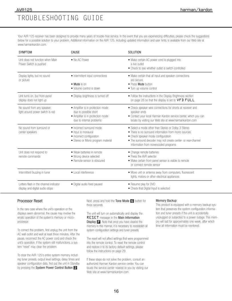
TROUBLESHOOTING GUIDE
SYMPTOM CAUSE SOLUTION
Unit does not function when Main • No AC Power • Make certain AC power cord is plugged into Power Switch is pushed a live outlet
• Check to see whether outlet is switch-controlled
Display lights, but no sound • Intermittent input connections • Make certain that all input and speaker connections or picture are secure
• Mute is on • Press Mute button• Volume control is down • Turn up volume control
Unit turns on, but front-panel • Display brightness is turned off • Follow the instructions in the Display Brightness section display does not light up on page 26 so that the display is set to VFD FULL
No sound from any speaker; • Amplifier is in protection mode • Check speaker wire connections for shorts at receiver and light around power switch is red due to possible short speaker ends
• Amplifier is in protection mode • Contact your local Harman Kardon service center, which you candue to internal problems locate by visiting our Web site at www.harmankardon.com
No sound from surround or • Incorrect surround mode • Select a mode other than Stereo or Dolby 3 Stereocenter speakers • Input is monaural • There is no surround information from mono sources
• Incorrect configuration • Check speaker mode configuratioin • Stereo or Mono program material • The surround decoder may not create center- or rear-channel
information from nonencoded programs
Unit does not respond to • Weak batteries in remote • Change remote batteriesremote commands • Wrong device selected • Press the AVR selector
• Remote sensor is obscured • Make certain front-panel sensor is visible to remoteor connect remote sensor
Intermittent buzzing in tuner • Local interference • Move unit or antenna away from computers, fluorescent lights, motors or other electrical appliances
Letters flash in the channel indicator • Digital audio feed paused • Resume play for DVDdisplay and digital audio stops • Check that Digital Input is selected
Processor Reset
In the rare case where the unit’s operation or the displays seem abnormal, the cause may involve theerratic operation of the system’s memory or micro-processor.
To correct this problem, first unplug the unit from theAC wall outlet and wait at least three minutes. After thepause, reconnect the AC power cord and check theunit’s operation. If the system still malfunctions, a sys-tem “reset” may clear the problem.
To clear the AVR 125’s entire system memory includ-ing tuner presets, output level settings, delay times andspeaker configuration data, first put the unit in Standbyby pressing the System Power Control Button 2.
Next, press and hold the Tone Mode 6 button forthree seconds.
The unit will turn on automatically and display theRESET message in the Main InformationDisplay F. Note that once you have cleared thememory in this manner, it is necessary to reestablish allsystem configuration settings and tuner presets.
The reset will not affect settings that were programmedinto the remote control. To reset the remote controland restore it to its factory default settings, please follow the instructions on page 29.
If these steps do not solve the problem, consult anauthorized Harman Kardon service center. You canlocate the service center nearest to you by visiting ourWeb site at www.harmankardon.com.
Memory BackupThis product is equipped with a memory backup sys-tem that preserves the system configuration informa-tion and tuner presets if the unit is accidentallyunplugged or subjected to a power outage. This mem-ory will last for approximately one week, after whichtime all information must be reentered.
Your AVR 125 receiver has been designed to provide many years of trouble-free service. In the event that you are experiencing difficulties, please check the suggestionsbelow for a possible solution to your problem. Additional information on the AVR 125, including updated information and user hints, is available from our Web site atwww.harmankardon.com.
16
AVR125 harman/kardon

1
2
3
4
5
6
7
8
12
13
14
15
18
11
8
10
9
19
23
24
23
24
25
2627
20
21
28
29
31
30
32
33
34
35
22
S2
S2
x3
x2
S3
S2
S1 x6
S2x3
x7S2
S2x13
S4x2
S4x2
S10x5
S5x2
S5x2
S7 x6
S1x7
x4S9
S5x2
x2S5
S5 x2
x2S4
S4
S4
S4
S6 x2
S11 x2
S10x2
S8x24
S1
S12 x3
38
40
16
25
17
42
SCREW,SPECIAL
SCREW,SPECIAL
SCREW
SCREW
SCREW
SCREW,TRANS
SCREWS10
S11
S12
S6
S7
S8
S9
SCREW
SCREW
SCREW
SCREW
DESCRIPTION
SCREWS1
S3
S4
S2
S5
NO
CTB4+6FFZ
CTB3+10GFZ
CTB3+6J
CHD2A012
CHD1A012Z
CTW3+12J
CHD1A023
CTB3+8JFZ
CTWS3+10G
CTB3+10G
CTW3+8J
CTB3+8J
PARTS NO. DIGITAL INPUT
BRIDGE DIODE
TR PCB
TRANS PCB
TRANS PCB
VIDEO PCB
INPUT PCB
CONNECTOR PCB
POWER LED PCB
MOMS PCB
MAIN PCB ASS'Y
INPUT PCB ASS'Y
PLATE,SHIELD A
417
4
2 42
24
4
2
6
40
WASHER
NUT
1
8
12
14
2838
39
Q,ty
39-3
39-8
39-6
39-4
CMC1A189
37-8
39-2
39-1
37-7
37-6
37-5
COP11518E
COP11517E
1
1
1
1
1
1
1
1
1
1
1
1
1
1
1
1CGU1A280XWINDOW,FIP2
PHONE PCB37-4 1
CLT5V030ZU
CKL1A069H43
CBC1A139YK128
CBT1A817K128
CBT1A819M7G2
CBT1A818YK128
CBT1A816M7G2
CGW1A337R4YK128
CBN1A156K128
KEY PCB
TONE PCB
FIP PCB
CKC1B128S1CABINET,TOP21
FRONT PCB ASS'Y
CHASSIS,BOTTOM
BUSHING,AC CORD
PANEL,REAR
BRACKET,PCB
TRANS,POWER
BRACKET,PCB(H/T)
BRACKET,TRANS
HOLDER,PCB
BRACKET,PCB
SUPPORT,CUSHION
RUBBER,CUSHION
CORD,POWER
31
36
37
33
34
35
32
26
29
30
27
28
24
25
22
23
HEAT SINK
FOOT
37-3
37-2
37-1
COP11516E
KHR1A028
CKF3A235Z
CMD1A387
CJA523FBY
CMY1A192
CMD1A416
CMD1A464
CHE170
CMD1A417
CUA1A213
CHG1A233
KHG1A050
PLATE,SHIELD
BRACKET,FLT
HOLDER,LED B
HOLDER,LED A
BRACKET,PCB
INDICATOR,POWER
KNOB,POWER
KNOB,DELAY
KNOB,FUNCTION
BRACKET,SIDE
PANEL,FRONT
BDAGE,HARMAN/KARDON
KNOB,ROTARY
CUSHION,RUBBER
19
20
17
18
14
15
16
12
13
KNOB,MOMS
7
9
10
11
8
6
5
4
3
KNOB,SET
SHEET,FIP
SHEET
CMD1A374
CMH1A168
CMH1A167
CHG1A157
CMC1A180
CMK1A010
CGL1A200
CMD1A443
KMZ1A76
KMZ1A077
KGB1A111Z
1
1
2
1
1
1
1
1
1
1
2
2
2
2
4
4
1
1
1
2
2
2
1
1
1
1
1
1
2
2
3
1
1
1
1
1
1
CBN1A155K128KNOB,VOLUME
DESCRIPTION
1
NO PARTS NO. Q,ty
1
4140
5
37-5
37-6
S2 x2
37-4
37-2
37-1
37-3
37-8
39-3
39-4
39-1
39-2
39-8
S5
S5
37-7
39-6
AVR125 Exploded View
17
AVR125 harman/kardon
KMZ176# HFLCM2054CF.I.P (DISPLAY)
JRico
Line
JRico
Line

AVR125/225 DISASSEMBLY PROCEDURE <1> TOP-CABINET(21) REMOVAL
1. Remove 13 screws(S1,S7) and then remove the Top-cabinet. <2> FRONT PANEL ASS’Y REMOVAL
1. Remove the Top-cabinet, referring to the previous step<1>. 2. Disconnect the connect (BN72-Card canle)) on the FP PCB(37-1) from connector(CN72) on the Input PCB(39-1) 3. Disconnect the lead wire(BN80-8P) on the FP PCB(37-1) from connector(CN80) on the Main PCB(38). 4.Disconnect the lead wire(BN16-8P,BN10-4P) on the Tone PCB(37-3) from connector(CN16,CN10) on the Connect
PCB(37-7). 5. Disconnect the lead wire(BN41-6P) on the Tone PCB(37-3) from connector(CN41) on the Video PCB(39-2). 6. Disconnect the lead wire(BN18-5P) on the Digital input PCB(37-8) from connector(CN18) on the Input PCB(39-1). 7. Disconnect the lead wire(BN81-6P,BN83-2P) on the FP PCB(37-1) from connector(CN81.CN83) on the
Trans PCB(39-3). 8. Disconnect the lead wire(BN88-2P) on the Main PCB(38) from connector(CN88) on the Moms PCB(37-5). 9. Remove 1 screw(S10) and then lead wire(JW82-2P) on the Phone PCB(37-4). 10. Remove 9 screws(S1) and then remove the Front Panel ASS’Y.
<3> TONE PCB(37-3) REMOVAL 1. Remove the Top-cabinet, referring to the previous step<1>.
2. Remove the Front Panel ASS’Y, referring to the previous step<2>. 3. Pull out the Volume Knob ASS’Y & 3 Rotary Knobs(5). 4. Remove 1 Nut(40), 1 Washer(41) 5. Remove 7 screws(S2) and then remove the Tone PCB(37-3). 6. Disconnect the lead wire(BN84-5P,BN90-2P) One the Tone PCB(37-3) from connector(CN84,CN90) on the FP PCB(37-1)
7. Disconnect the lead wire (BN87-6P) One the Tone PCB(37-3) from connector(CN87) on the Phone PCB(37-4)
<4>PHONE PCB(37-4) REMOVAL 1. Remove the Top-cabinet, referring to the previous step<1>.
2. Remove the Front Panel ASS’Y, referring to the previous step<2>. 3. Disconnect the lead wire (BN87-6P) One the Tone PCB(37-3) from connector(CN87) on the Phone PCB(37-4) 4. Remove 2 screws(S2,S3) and then remove the Phone PCB(37-4) .
<5>POWER LED PCB(37-6) REMOVAL 1. Remove the Top-cabinet, referring to the previous step<1>.
2. Remove the Front Panel ASS’Y, referring to the previous step<2>. 3. Remove 2 screws(S2) and then remove the Power led PCB(37-6). 4. Disconnect the lead wire(BN88-4P) from connector(CN88) on the FP PCB(37-1).
<6>FRONT PCB(37-1) REMOVAL 1. Remove the Top-cabinet, referring to the previous step<1>.
2. Remove the Front Panel ASS’Y, referring to the previous step<2>. 3. Remove the Tone PCB(37-3), referring to the previous step<3>. 4. Remove the Phone PCB(37-4), referring to the previous step<4>. 5. Remove the Power led PCB(37-6), referring to the previous step<5>. 6. Remove 6 screws(S2) and then remove the Front PCB(37-1)
18
AVR125 harman/kardon

<7>TUNER MODULE(40) REMOVAL 1. Remove the Top-cabinet, referring to the previous step<1>.
2. Disconnect the connector(CON1-Card cable) from connector(CN13) on the Input PCB ASS’Y(39-1). 3. Remove 2 screws(S8) and then remove the Tuner Module(40).
<8>VIDEO PCB(39-2) REMOVAL 1. Remove the Top-cabinet, referring to the previous step<1>. 2. Disconnect the lead wire(BN41-6P) on the Tone PCB(37-3) from connector(CN41) on the Video PCB(39-2). 3.Disconnect the connector (CN15-Card cable) on the Input PCB(39-1) from lead wire(CN43) on the Video PCB(39-2). 4. Remove 6 screws(S8) and then remove the Video PCB(39-2).
<9>INPUT PCB(39-1) REMOVAL 1. Remove the Top-cabinet, referring to the previous step<1>.
2. Remove the Connect PCB(37-7). 3. Disconnect the lead wire(BN18-5P) on the Digital input PCB(37-8) from connector(CN18) on the Input PCB(39-1). 4. Disconnect the connect (BN72-Card canle)) on the FP PCB(37-1) from connector(CN72) on the Input PCB(39-1) 5. Remove 13 screws(S8,S11) and then remove the Input PCB(39-1).
<10>POWER TRANS(31) REMOVAL
1. Remove the Top-cabinet, referring to the previous step<1>. 2. Disconnect the connector (CN20,BN96) on the Trans PCB from lead wire(CN20-3P,BN96-6P) on the Main PCB(38).
3. Remove 1 screw(S5) and then remove the Tr PCB(39-6) 4. Remove 1 screw(S5) and then remove the Bridge Diode PCB(39-8) 3. Remove 4 Trans screws(S9) and then remove the Power Trans(31).
<11>MAIN PCB ASS’Y(38) REMOVAL
1. Remove the Top-cabinet, referring to the previous step<1>. 2. Remove the Tuner module, referring to the previous step<7>. 3. Remove the Video PCB, referring to the previous step<8>. 4. Remove the Input PCB, referring to the previous step<9>. 5. Disconnect the lead wire(BN80-8P) on the FP PCB(37-1) from connector(CN80) on the Main PCB(38). 6. Disconnect the lead wire(BN88-2P) on the Main PCB(38) from connector(CN88) on the Moms PCB(37-5). 7. Disconnect the connector (CN20,BN96) on the Trans PCB from lead wire(CN20-3P,BN96-6P) on the Main PCB(38)..
8. Remove 11screws(S1-1EA, S4-2EA, S6-2EA, S8-6EA) and then remove the Main PCB ASS’Y(38).
19
AVR125 harman/kardon

3) PRINCIPAL PARTS LOACTION
MODULETUNER
DISASSEMBLY
2) REMOVAL OF FRONT PANEL
1) REMOVAL OF TOP COVER
FRONT PCB
TRANS FORMERINPUT PCB
MAIN PCB
20
AVR125 harman/kardon

AMPLIFIER SECTION BIAS ADJUSTMENT
CUP11517X (MAIN PCB)
Measurement condition. No input signal or volume position is minimum.
Standard value.. Ideal current = 48mA ( ± 5%). Ideal DC Voltage = 21.12mV ( ± 5%)
DC VOLTMETER..............Connect to CN61, CN62, CN63, CN64, CN65
NO. Channel Adjust for Adjustment
1 Front Left 21.12mV (±5%) VR61
CN61
VR61
2 Front Right 21.12mV (±5%)
21.12mV (±5%)
21.12mV (±5%)
21.12mV (±5%)
VR62
CN62
VR62
3 Center VR63
CN63
VR63
4 Surround Left VR64
CN64
VR64
5 Surround Right VR65
VR65
CN65
21
AVR125 harman/kardon

22
AVR125 harman/kardon

Input
Selector
ClockRecovery Clock
Generator
DAIF
Decoder
AC-3/MPEG
Detect
DEM
µP I/F
Audio
I/F
X'tal
Oscillator
PDN
INT0 P/S=”L”
LRCK
BICK
SDTO
DAUX
MCKO2
XTOXTIRAVDDAVSS
CDTI
CDTO
CCLK
CSNDVDD
DVSSTVDD
MCKO1
IIC
RX0
RX1
RX2
RX3RX4
RX5
RX6
RX7
DIT
TX0
Error &
DetectSTATUS
INT1
Q-subcode
buffer
TX1
B,C,U,VOUT
8 to 3
VIN
Serial Control Mode
InputSelector
ClockRecovery Clock
Generator
DAIF
Decoder
AC-3/MPEG
Detect
DEM
Audio
I/F
X'tal
Oscillator
PDN
INT0 P/S=”H”
LRCK
BICK
SDTO
DAUX
XTOXTIRAVDDAVSS
CM1
CM0
OCKS1
OCKS0
DVDD
DVSSTVDD
IPS1
RX0
RX1
RX2
RX3
IPS0
DIF0
DIF1
DIF2
DIT
TX0
Error &
DetectSTATUS
INT1
TX1
B,C,U,VOUT
4 to 2
VIN
MCKO2
MCKO1
Parallel Control Mode
23
AVR125 harman/kardon
이종배
BLOCK DIAGRAM

IPS0/RX4R
X3
1
AVSS
48
2
DIF0/RX5 3
TEST2 4
DIF1/RX6 5
AVSS 6
DIF2/RX7 7
IPS1/IIC 8
P/SN 9
XTL0 10
XTL1
AV
SS
47
RX
246 45 44
AV
SS
43
RX
042
AV
SS
41
VC
OM
40
R39
AV
DD
38
TV
DD
13
NC
14
TX
015
TX
116
BO
UT
17 18
UO
UT
19
VO
UT
20
DV
DD
21
DV
SS
22
MC
KO
123
36
35
34
33
32
31
30
29
28
27
26
INT0
OCKS0/CSN/CAD0
OCKS1/CCLK/SCL
CM1/CDTI/SDA
CM0/CDTO/CAD1
PDN
XTI
XTO
DAUX
MCKO2
BICK
AK4114VQ
Top View
CO
UT
TE
ST
1
RX
1
INT
137
LRC
K24
11
VIN 12 25 SDTO
24
AVR125 harman/kardon
이종배
DIR IC PIN ASSIGNMENT & BLOCK DIAGRAM PIN ASSIGNMENT (TOP VIEW)

PIN/FUNCTION
No. Pin Name I/O Function
IPS0 I Input Channel Select 0 Pin in Parallel Mode 1
RX4 I Receiver Channel 4 Pin in Serial Mode (Internal biased pin)
2 NC(AVSS) I No Connect
No internal bonding. This pin should be connected to AVSS.
DIF0 I Audio Data Interface Format 0 Pin in Parallel Mode 3
RX5 I Receiver Channel 5 Pin in Serial Mode (Internal biased pin)
4 TEST2 I TEST 2 pin
This pin should be connect to AVSS.
DIF1 I Audio Data Interface Format 1 Pin in Parallel Mode 5
RX6 I Receiver Channel 6 Pin in Serial Mode (Internal biased pin)
6 NC(AVSS) I No Connect
No internal bonding. This pin should be connected to AVSS.
DIF2 I Audio Data Interface Format 2 Pin in Parallel Mode 7
RX7 I Receiver Channel 7 Pin in Serial Mode (Internal biased pin)
IPS1 I Input Channel Select 1 Pin in Parallel Mode
8 IIC I
IIC Select Pin in Serial Mode.
“L”: 4-wire Serial, “H”: IIC
9 P/SN I Parallel/Serial Select Pin
“L”: Serial Mode, “H”: Parallel Mode
10 XTL0 I X’tal Frequency Select 0 Pin
11 XTL1 I X’tal Frequency Select 1 Pin
12 VIN I V-bit Input Pin for Transmitter Output
13 TVDD I Input Buffer Power Supply Pin, 3.3V or 5V
14 NC I No Connect
No internal bonding. This pin should be open or connected to DVSS.
15 TX0 O Transmit Channel (Through Data) Output 0 Pin
16 TX1 O When TX bit = “0”, Transmit Channel (Through Data) Output 1 Pin.
When TX bit = “1”, Transmit Channel (DAUX Data) Output Pin (Default).
17 BOUT O Block-Start Output Pin for Receiver Input
“H” during first 40 flames.
18 COUT O C-bit Output Pin for Receiver Input
19 UOUT O U-bit Output Pin for Receiver Input
20 VOUT O V-bit Output Pin for Receiver Input
21 DVDD I Digital Power Supply Pin, 3.3V
22 DVSS I Digital Ground Pin
23 MCKO1 O Master Clock Output 1 Pin
24 LRCK I/O Channel Clock Pin
25 SDTO O Audio Serial Data Output Pin
26 BICK I/O Audio Serial Data Clock Pin
27 MCKO2 O Master Clock Output 2 Pin
28 DAUX I Auxiliary Audio Data Input Pin
29 XTO O X'tal Output Pin
30 XTI I X'tal Input Pin
25
IC PIN FUNCTION AK4114VQ IC75AVR125 harman/kardon

PIN/FUNCTION (Continued)
No. Pin Name I/O Function
31 PDN IPower-Down Mode Pin
When “L”, the AK4114 is powered-down and reset.
CM0 I Master Clock Operation Mode 0 Pin in Parallel Mode
CDTO O Control Data Output Pin in Serial Mode, IIC= “L”.32
CAD1 I Chip Address 1 Pin in Serial Mode, IIC= “H”.
CM1 I Master Clock Operation Mode 1 Pin in Parallel Mode
CDTI I Control Data Input Pin in Serial Mode, IIC= “L”.33
SDA I/O Control Data Pin in Serial Mode, IIC= “H”.
OCKS1 I Output Clock Select 1 Pin in Parallel Mode
CCLK I Control Data Clock Pin in Serial Mode, IIC= “L”34
SCL I Control Data Clock Pin in Serial Mode, IIC= “H”
OCKS0 I Output Clock Select 0 Pin in Parallel Mode
CSN I Chip Select Pin in Serial Mode, IIC=”L”.35
CAD0 I Chip Address 0 Pin in Serial Mode, IIC= “H”.
36 INT0 O Interrupt 0 Pin
37 INT1 O Interrupt 1 Pin
38 AVDD I Analog Power Supply Pin, 3.3V
39 R -External Resistor Pin
18kΩ +/-1% resistor should be connected to AVSS externally.
40 VCOM -Common Voltage Output Pin
0.47µF capacitor should be connected to AVSS externally.
41 AVSS I Analog Ground Pin
42 RX0 IReceiver Channel 0 Pin (Internal biased pin)
This channel is default in serial mode.
43 NC(AVSS) INo Connect
No internal bonding. This pin should be connected to AVSS.
44 RX1 I Receiver Channel 1 Pin (Internal biased pin)
45 TEST1 ITEST 1 pin.
This pin should be connected to AVSS.
46 RX2 I Receiver Channel 2 Pin (Internal biased pin)
47 NC(AVSS) INo Connect
No internal bonding. This pin should be connected to AVSS.
48 RX3 I Receiver Channel 3 Pin (Internal biased pin)
Note 1. All input pins except internal biased pins should not be left floating.
26
AVR125 harman/kardon

LOUT1-R
OU
T1+
1
LOUT1+
44
2
DZFL2 3
DZFR1 4
DZFL1 5
CAD0 6
CAD1 7
PDN 8
BICK 9
MCLK 10
DVDD 11
RO
UT
1-43
LOU
T2+
42
LOU
T2-
41
RO
UT
2+40
RO
UT
2-39
LOU
T3+
38
LOU
T3-
37
RO
UT
3+36
RO
UT
3-35
AV
SS
34
DV
SS
12
SD
TI1
13
SD
TI2
14
SD
TI3
15
LRC
K16
SM
UT
E17
CC
LK18
CD
TI
19
CS
N20
DF
S0
21
CK
S0
22
33
32
31
30
29
28
27
26
25
24
23
AVDD
VREFH
DZFR2
DZFL3
DZFR3
DZFE
DIF2
DIF1
DIF0
CKS2
CKS1
AK4356VQ
Top View
n Block Diagram
SCF DAC DATT
DZFL1LOUT1+LOUT1-
SCF DAC DATT
DZFR1ROUT1+ROUT1-
SCF DAC DATT
DZFL2LOUT2+LOUT2-
SCF DAC DATT
DZFR2ROUT2+ROUT2-
SCF DAC DATT
DZFL3LOUT3+LOUT3-
SCF DAC DATT
DZFR3ROUT3+ROUT3-
AudioI/F
ControlRegister
AK4356
MCLK
LRCK
BICK
MCKOLRCK
BICK
XTI
XTO
Controller
CSCCLK
CDTI
LRCK
BICK
SDOUT1
SDOUT2SDOUT3
AC3
SDTI1
SDTI2SDTI3
27
AVR125 harman/kardon
이종배
D/A CONVERTER IC PIN ASSIGNMENT & BLOCK DIAGRAM PIN ASSIGNMENT (TOP VIEW)

PIN/FUNCTION
No. Pin Name I/O Function1 LOUT1- O DAC1 Lch Negative Analog Output Pin2 LOUT1+ O DAC1 Lch Positive Analog Output Pin3 DZFL2 O DAC2 Lch Zero Input Detect Pin4 DZFR1 O DAC1 Rch Zero Input Detect Pin5 DZFL1 O DAC1 Lch Zero Input Detect Pin6 CAD0 I Chip Address 0 Pin7 CAD1 I Chip Address 1 Pin8 PDN I Power-Down & Reset Pin
When “L”, the AK4356 is powered-down and the control registers are reset to default state. If the state of CAD0-1 changes, then the AK4356 must be reset by PDN.
9 BICK I Audio Serial Data Clock Pin10 MCLK I Master Clock Input Pin11 DVDD - Digital Power Supply Pin, +4.75~+5.25V12 DVSS - Digital Ground Pin13 SDTI1 I DAC1 Audio Serial Data Input Pin14 SDTI2 I DAC2 Audio Serial Data Input Pin15 SDTI3 I DAC3 Audio Serial Data Input Pin16 LRCK I Audio Input Channel Clock Pin17 SMUTE I Soft Mute Pin (Note)
When this pin goes to “H”, soft mute cycle is initialized. When returning to “L”, the output mute releases.
18 CCLK I Control Data Clock Pin19 CDTI I Control Data Input Pin20 CSN I Chip Select Pin
This pin should be held to “H” except for access.
28
AVR125 harman/kardon
이종배
D/A CONVERTER IC PIN FUNCTION (AK4356VQ) : IC78

No. Pin Name I/O Function21 DFS0 I Double Speed Sampling Mode 0 Pin (Note)
“L”: Normal Speed, “H”: Double Speed at DFS1 bit = “0”.22 CKS0 I Input Clock Select 0 Pin (Note)23 CKS1 I Input Clock Select 1 Pin (Note)24 CKS2 I Input Clock Select 2 Pin (Note)25 DIF0 I Audio Data Interface Format 0 Pin (Note)26 DIF1 I Audio Data Interface Format 1 Pin (Note)27 DIF2 I Audio Data Interface Format 2 Pin (Note)28 DZFE I Zero Input Detect Enable Pin (Note)29 DZFR3 O DAC3 Rch Zero Input Detect Pin30 DZFL3 O DAC3 Lch Zero Input Detect Pin31 DZFR2 O DAC2 Rch Zero Input Detect Pin32 VREFH I Positive Voltage Reference Input Pin, AVDD33 AVDD - Analog Power Supply Pin34 AVSS - Analog Ground Pin, +4.75~+5.25V35 ROUT3- O DAC3 Rch Negative Analog Output Pin36 ROUT3+ O DAC3 Rch Positive Analog Output Pin37 LOUT3- O DAC3 Lch Negative Analog Output Pin38 LOUT3+ O DAC3 Lch Positive Analog Output Pin39 ROUT2- O DAC2 Rch Negative Analog Output Pin40 ROUT2+ O DAC2 Rch Positive Analog Output Pin41 LOUT2- O DAC2 Lch Negative Analog Output Pin42 LOUT2+ O DAC2 Lch Positive Analog Output Pin43 ROUT1- O DAC1 Rch Negative Analog Output Pin44 ROUT1+ O DAC1 Rch Positive Analog Output Pin
Note:SMUTE, DFS0, CKS0, CKS1, CKS2, DIF0, DIF1, DIF2, DZFE pins are ORed with serial control register.
29
AVR125 harman/kardon

November 1988
Revised November 1999
74AC
04 • 74AC
T04 H
ex Inverter
74AC04 • 74ACT04 Hex Inverter
General DescriptionThe AC/ACT04 contains six inverters.
Features ICC reduced by 50% on 74AC only
Outputs source/sink 24 mA
ACT04 has TTL-compatible inputs
Ordering Code:
Device also available in Tape and Reel. Specify by appending suffix letter “X” to the ordering code. (PC not available in Tape and Reel.)
Logic Symbol
IEEE/IEC
Connection Diagram
Pin Descriptions
FACT is a trademark of Fairchild Semiconductor Corporation.
Order Number Package Number Package Description
74AC04SC M14A 14-Lead Small Outline Integrated Circuit (SOIC), JEDEC MS-120, 0.150” Narrow Body
74AC04SJ M14D 14-Lead Small Outline Package (SOP), EIAJ TYPE II, 5.3mm Wide
74AC04MTC MTC14 14-Lead Thin Shrink Small Outline Package (TSSOP), JEDEC MO-153, 4.4mm Wide
74AC04PC N14A 14-Lead Plastic Dual-In-Line Package (PDIP), JEDEC MS-001, 0.300” Wide
74ACT04SC M14A 14-Lead Small Outline Integrated Circuit (SOIC), JEDEC MS-120, 0.150” Narrow Body
74ACT04MTC MTC14 14-Lead Thin Shrink Small Outline Package (TSSOP), JEDEC MO-153, 4.4mm Wide
74ACT04PC N14A 14-Lead Plastic Dual-In-Line Package (PDIP), JEDEC MS-001, 0.300” Wide
Pin Names Description
An Inputs
On Outputs
30
AVR125 harman/kardon
최동찬
74ACT04SC : IC83, 84
최동찬

∆ΣModulator
MCLK
AINLLRCK
SCLK
SDTO
DIF
VCOM
Clock Divider
AINR
AGNDVA
DecimationFilter
Serial I/OInterface
Voltage Reference
TTL
DGNDVD
TST
∆ΣModulator
DecimationFilter
PDN
1AINR
AINL
VCOM
NC
AGND
VA
VD
DGND
TopView
2
3
4
5
6
7
8
TST
TTL
PDN
DIF
SCLK
MCLK
LRCK
SDTO
16
15
14
13
12
11
10
9
31
AVR125 harman/kardon
최동찬
BLOCK DIAGRAM

PIN/FUNCTION
No. Pin Name I/O Description
1 AINR I Rch Analog Input Pin
2 AINL I Lch Analog Input Pin
3 NC - NC Pin
No internal bonding.
4 VCOM O Common Voltage Output Pin
Normally connected to AGND with a 0.1µF ceramic capacitor in parallel with an
electrolytic capacitor less than 2.2µF.
5 AGND - Analog Ground Pin, 0V
6 VA - Analog Power Supply Pin, +4.5∼ +5.5V
7 VD - Digital Power Supply Pin, +2.7∼ +5.5V(fs=48kHz), +4.5∼ +5.5V(fs=96kHz)
8 DGND - Digital Ground Pin, 0V
9 SDTO O Serial Data Output Pin
Data bits are presented MSB first, in 2’s complement format.
This pin is “L” in the power-down mode.
10 LRCK I Left/Right Channel Select Pin
The fs clock is input to this pin.
11 MCLK I Master Clock Input Pin
12 SCLK I Serial Data Input Pin
Output data is clocked out on the falling edge of SCLK.
13 PDN I Power-Down Pin
When “L”, the circuit is in power-down mode.
The AK5380 should always be reset upon power-up.
14 DIF I Serial Interface Format Pin
“L”: MSB justified, “H”: I2S
15 TTL I Digital Input Level Select Pin
“L”: CMOS level (VD=2.7∼ 5.5V), “H”: TTL level (VD=4.5∼ 5.5V)
16 TST I Test Pin (Internal pull-down pin)
This pin should be left open.
Note: All input pins except pull-down pins should not be left floating.
32
AVR125 harman/kardon
이종배
A/D CONVERTER IC PIN FUNCTION (AK5380VT) : IC77

PIN ASSIGNMENT (74HCU04AFN : IC71,72 )
LOGIC SYMBOL
TRUTH TABLE
1
2
3
4
5
6
7
1A
1Y
2A
2Y
3A
3Y
GND
6A
6Y
5A
5Y
4A
4Y
Vcc14
13
12
11
10
9
8
A
L
H
Y
H
L
1A(1)
(3)
(5)
(9)
(11)
(13)
2A
3A
4A
5A
6A
1Y
2Y
3Y
4Y
5Y
6Y
(2)
(4)
(6)
(8)
(10)
(12)
33
AVR125 harman/kardon

CM2054C Ise Electronics Corporation:Display Pattern Scale 3:1Unit : mm
Sheet 3/5
100.0
17.0
G:Green /(Blue Green)
Rsh.O-N:Reddish Orange-N/(Red)
Color of illumination

AVR125 harman/kardon

AVR125 harman/kardon

PIN No. Pin Name I/O Function1,12,23 +VD1 - Digital Power supply. Normally +2.5v
2,13,24 DGND - Digital Ground
3 AUD3 O SPDIF transmitter output/Digital audio output(N.C)
4 WR I Host write strobe pin(connected to GND with an external resistor)
5 RD I Host parallel output enable pin(pulled up with an external resistor)
6 CS_DA I SPI Serial data input pin
7 CS_CK I Serial control clock input pin
8 EMAD7 I/O
9 EMAD6 I/O
10 EMAD5 I/O
11 EMAD4 I/O Serial data IN/OUTPUT pins(pulled up with an external resistor)
14 EMAD3 I/O
15 EMAD2 I/O
16 EMAD1 I/O
17 EMAD0 I/O
18 CS_CE I Host parallel chip select pin
19 SCDIO(AK_DOUT) O Serial control port data ouput pin
20 INTREQ O Control port interrupt request output pin
21 EXTMEM I/O External Memory Chip Selector(pulled up with an external resistor)
22 SDATAN1(SDI) I PCM audio data input number 1 pin
25 SCLKN1(BICK) I PCM audio input bit clock pin
26 LRCLKN1(LRCK) I PCM audio input sample rate clock pin
27 CMPDAT(SDI) I PCM audio data input number 2 pin
28 CMPCLK(BICK) I PCM audio input bit clock pin
29 CREQ(LRCK) I PCM audio input sample rate clock pin
30 CLKIN(XIN) I Master clock input(used external clock)
31 CLKSEL(GND) I DSP clock mode select pin: connect the GND
32 FILT1 Connects to an external filter for the on-chip phase-locked loop
33 FILT1 Connects to an external filter for the on-chip phase-locked loop
34 +2.5V - Analog Power supply for clock generator . Normally +2.5V
35 AGND - Analog ground supply for clock generator PLL.
36 RESET(CS_RST) I Master reset input pin
37 DBDATA - Reserved pin and should be pulled up with an external resistor.
38 DBCLK - Reserved pin and should be pulled up with an external resistor.
39 AUD2(SDO2) O PCM multi-format digital-audio data ouput2 pin
40 AUD1(SDO1) O PCM multi-format digital-audio data ouput1 pin
41 AUD0(SDO0) O PCM multi-format digital-audio data ouput0 pin
42 LRCLK I Audio output sample rate clock pin
43 SCLK(BICK) I Audio ouput bit clock pin
44 MCLK I Audio master clock output pin
AUDIO DSP (CS493263 - CLG : IC79)
37
AVR125 harman/kardon
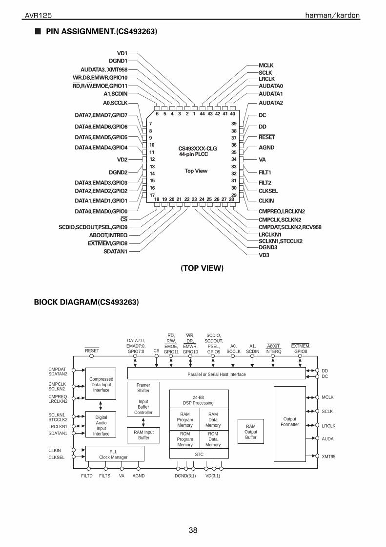
CMPDATSDATAN2
CMPCLKSCLKN2
CMPREQLRCLKN2
SCLKN1STCCLK2
LRCLKN1SDATAN1
CLKIN
CLKSEL
FILTD FILTS VA AGND DGND(3:1) VD(3:1)
XMT95
AUDA
LRCLK
SCLK
MCLK
DCDD
EXTMEM.GPIO8
A800TINTERQ
A1,SCDIN
A0,SCCLKCS
STC
Parallel or Serial Host Interface
RESET
SCDIO,SCDOUT,
PSEL,GPIO9
WR,DR,
EMWR,GPIO10
RD,R/W,
EMOE,GPIO11
DATA7:0,EMAD7:0,GPIO7:0
CompressedData InputInterface
RAMProgramMemory
ROMProgramMemory
RAMData
Memory RAMOutputBuffer
OutputFormatter
ROMData
Memory
PLLClock Manager
RAM InputBuffer
24-BitDSP Processing
DigitalAudioInput
Interface
FramerShifter
InputBuffer
Controller
PIN ASSIGNMENT.(CS493263)
(TOP VIEW)
BlOCK DIAGRAM(CS493263)
VD1
DGND1
AUDATA3, XMT958
WR,DS,EMWR,GPIO10
RD,R/W,EMOE,GPIO11
A1,SCDIN
A0,SCCLK
DATA7,EMAD7,GPIO7
CS493XXX-CLG44-pin PLCC
Top View
DATA6,EMAD6,GPIO6
DATA5,EMAD5,GPIO5
DATA4,EMAD4,GPIO4
DATA3,EMAD3,GPIO3
DATA2,EMAD2,GPIO2
DATA1,EMAD1,GPIO1
DATA0,EMAD0,GPIO0
VD2
DGND2
CS
SCDIO,SCDOUT,PSEL,GPIO9
ABOOT,INTREQ
EXTMEM,GPIO8
SDATAN1
MCLK
SCLKLRCLK
AUDATA0
AUDATA1
AUDATA2
DC
7
8
9
10
11
12
13
14
15
16
1718 19 20 21 22 23 24 25 26 27 28
6 5 4 3 2 1 44 43 42 41 40
39
38
37
36
35
34
33
32
31
30
29
DD
RESET
AGND
FILT2
CLKSEL
CLKIN
CMPREQ,LRCLKN2
VA
FILT1
CMPDAT,SCLKN2,RCV958
CMPCLK,SCLKN2
LRCLKN1
VD3
SCLKN1,STCCLK2DGND3
38
AVR125 harman/kardon

No. 5606-3/13
Top view
LEVE
L SH
IFTE
R
21
2
1
3
4
2
5
6
3
7
4
1
2
1
3
4
2
5
6
3
7
4
1
3
4
5
6
7
8
9
10
14 28
11
12
13
27
26
25
24
23
22
21
20
19
18
17
16
15
LATC
H CI
RCUI
T
SHIFT REGISTER LE
VEL
SHIF
TER
LATC
H CI
RCUI
T
L-S R-S
Vss GND VDD
L-S
L-COM
L-S
L-S
L-COM
L-S
L-S
L-COM
L-S
L-COM
ST
R-S
R-COM
R-S
R-S
R-COM
R-S
R-S
R-COM
R-S
R-COM
DATA
CK
TC9162AF (FUNCTION/INPUT : IC30)
BLOCK DIAGRAM
TC9162AF (FUNCTION/INPUT : IC30)
BLOCK DIAGRAM
39
AVR125 harman/kardon
이종배
PIN ASSIGNMENT (TOP VIEW)
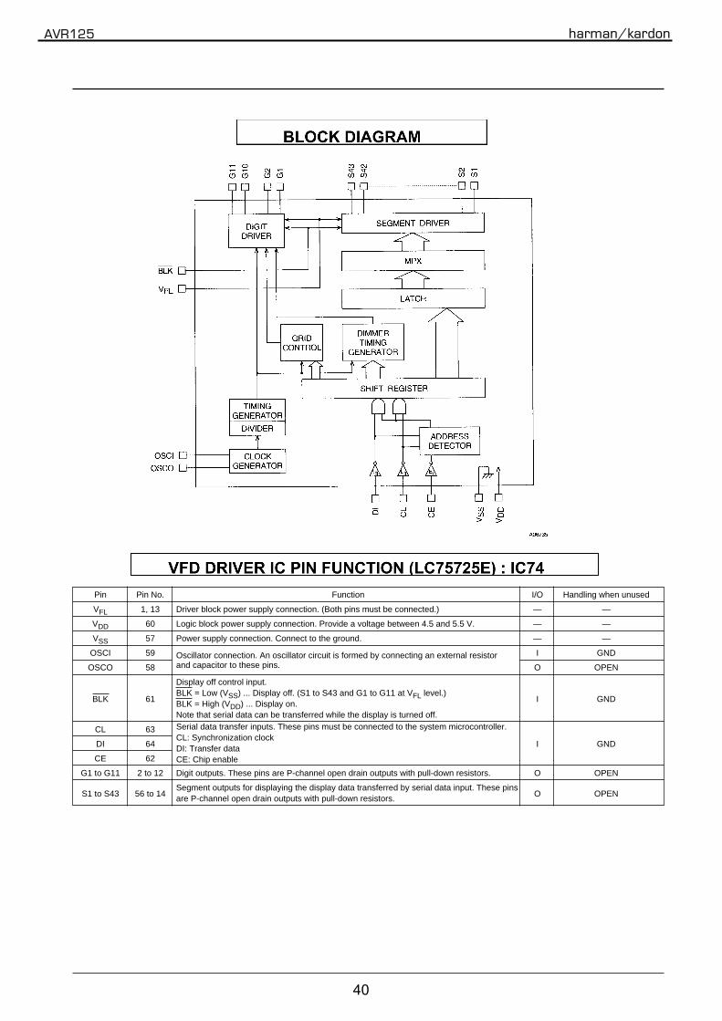
Pin Pin No. Function I/O Handling when unused
VFL 1, 13 Driver block power supply connection. (Both pins must be connected.) — —
VDD 60 Logic block power supply connection. Provide a voltage between 4.5 and 5.5 V. — —
VSS 57 Power supply connection. Connect to the ground. — —
OSCI 59 Oscillator connection. An oscillator circuit is formed by connecting an external resistor I GND
OSCO 58 and capacitor to these pins. O OPEN
Display off control input.
BLK 61BLK = Low (VSS) ... Display off. (S1 to S43 and G1 to G11 at VFL level.)
I GNDBLK = High (VDD) ... Display on.Note that serial data can be transferred while the display is turned off.
CL 63
DI 64 I GND
CE 62
G1 to G11 2 to 12 Digit outputs. These pins are P-channel open drain outputs with pull-down resistors. O OPEN
S1 to S43 56 to 14Segment outputs for displaying the display data transferred by serial data input. These pins
O OPENare P-channel open drain outputs with pull-down resistors.
Serial data transfer inputs. These pins must be connected to the system microcontroller.CL: Synchronization clockDI: Transfer dataCE: Chip enable
40
AVR125 harman/kardon
이종배
BLOCK DIAGRAM
이종배
VFD DRIVER IC PIN FUNCTION (LC75725E) : IC74

1-6
Fig. 1.1 Block Diagram (MB90470)
P00 to P07 (8): Provided with input pull-up resistor setting register
P10 to P17 (8): Provided with input pull-up resistor setting register
P40 to P47 (8): Provided with open-drain setting register
P70 to P75 (6): Provided with open-drain setting register
P76 to P77 (2): Open-drain
Note: In the figure above, the I/O port shares the pins with each internal functional block. When the pinsare used as internal module pins, they cannot be used as I/O port pins.
X0, X1 RSTXX0, X1A 5
CPU
F2MC-16LX family core
Communicationprescaler
UART
A/D converter(10 bits)
I/O expandedserial
interface x 2channels
SIN1, 2
SOT1, 2
SCK1, 2
AVCC
AVRH. L
AVSS
ADTG
AN0 to 7
Interrupt controller
8-/16-bit PPG
PPG0, 1
PPG2, 3
PPG4, 5
8-/16-bits UD counter
IN0, 1
OUT0, 1, 2,
3, 4, 5
16-bit reload timer
x 2 channels
TIN0
TOT0
External interrupt IRQ0 to 78
I/O timer
16-bit input capture x 216-bit output conveyer x 6
16-bit free-run timer
I2C interfaceSCL
SDA
I/O port
µPG
P00 P10 P20 P30 P40 P50 P60 P70 P80 P90 PA0
P07 P17 P27 P37 P47 P57 P67 P77 P87 P97 PA3
8 8 8 8 8 8 8 8 8 8 4
AIN0, 1
BIN0, 1
ZIN0, 1
EXTC
MT00
MT01
16-bit PWC
3 channels
PWC0
PWC1
PWC2
Chip select CS0, 1, 2, 3
2
Clock controlcircuit
RAM
ROM
EI2OS
SIN0
SOT0
SCK0
41
AVR125 harman/kardon
이종배
BLOCK DIAGRAM

1-7
P20-27/P30-37/P40-47/P70-77: 5 V-I/F
2
1
15
14
13
Vss
P63/A
N3
P62/A
N2
P61/A
N1
P60/A
N0
AV
RH
AV
cc
P77/S
DA
P76
/S
CL
P75
/PW
C2
P74
/TO
T0
AV
ss
P13/A
D11/D
11
P10/A
D08/D
08
P06/A
D06/D
06
P04/A
D04/D
04
P05/A
D05/D
05
P07/A
D07/D
07
P16/A
D14/D
14
P15/A
D13/D
13
P14/A
D12/D
12
P12/A
D10/D
10
P17/A
D15/D
15
P23/A19
P22/A18 P57/CLK
RSTX
P55/HAKX
P54/HRQ
P53/WRHX
P52/WRLX
P51/RDX
P50/ALE
PA3/OUT3
PA2/OUT2
P31/A01/BIN0
P30/A00/AIN0
P27/A23/PPG3
X0A
Vss
X1AP21/A17
P24/A20/PPG0
P25/A21/PPG1
P20/A16
P26/A22/PPG2
4
3
6
5
8
7
10
9
12
11
79
80
77
78
75
76
73
74
71
72
69
70
99
100 97
98
95
96
93
94
91
92
89
90
17
16
30
29
28
19
18
21
20
23
22
25
24
27
26
87
88
85
86
81
82
83
84
67
68
65
66
63
64
61
62
59
60
57
58
55
56
53
54
51
52
3231
34
33
36
35
38
37
40
39
42
41
44
43
46
45
50
49
48
47
P33/A03/AIN1
P32/A02/ZIN0
P37/A07/PWC1
P34/A04/BIN1
P35/A05/ZIN1
P36/A06/PWC0
P43/A11/MT00
P42/A10/SCK2
P46/A14/OUT4
P41/A09/SOT2
P44/A12/MT01
Vcc5
P40/A08/SIN2
P45/A13/EXTC
P47/A15/OUT5
P73/TIN0
P71/SOT0
P72/SCK0
MD
1
MD
0
P81
/IR
Q1
P80
/IR
Q0
P67/A
N7
P65/A
N5
P64/A
N4
P66/A
N6
P97/IN1
P96/IN0
P95/PPG5
P94/PPG4
P93/FRCK/ADTG/CS3
P92/SCK1/CS2
P91/SOT1/CS1
P90/SIN1/CS0
P87/IRQ7
P86/IRQ6
PA1/OUT1
PA0/OUT0
P85/IRQ5
P84/IRQ4
P83/IRQ3
P82/IRQ2
MD2
P03/A
D03/D
03
P00/A
D00/D
00
X1
Vss
X0
Vcc
3
P01/A
D01/D
01
P02/A
D02/D
02
QFP- 10 0(TOP VIEW)
P11/A
D09/D
09
P70/SIN0
P56/RDY
42
AVR125 harman/kardon
이종배
M-COM IC PIN ASSIGNMENT & BLOCK DIAGRAM PIN ASSIGNMENT (TOP VIEW)

LQFP QFP Pin Name Circuit Type Function
80 82 X0 A Oscillator pin
81 83 X1 A Oscillator pin
78 80 X0A A 32 kMHz Oscillator pin
77 79 X1A A 32 kMHz Oscillator pin
75 77 RSTX B Reset input pin
P00 to P07General-purpose I/O portsA pull-up resistor can be attached using the pull-up resistor settingregister (RDR0) (RD07 to RD00 = 1). (Invalid when set to output)
AD00 toAD07
In the multiplex mode, the pins function as external address/data buslower I/O pins.
83 to 90 85 to 92
D00 to D07
C(CMOS)
In the non-multiplex mode, they function as external data bus loweroutput pins.
P10 to P17General-purpose I/O portsA pull-up resistor can be attached using the pull-up resistor settingregister (RDR1) (RD17 to RD10 = 1). (Invalid when set to output)
AD08 toAD15
In the multiplex mode, the pins function as external address/data busupper I/O pins.
91 to 9893 to100
D08 to D15
C(CMOS)
In the non-multiplex mode, they function as external data upper outputpins.
P20 to P23General-purpose I/O portsWhen the corresponding bit of the HACR register is 0, the pins functionas address upper output pins (A20 to A23).
A16 to A19When the multiplex mode is enabled and the corresponding bit of theHACR register is 1, the pins function as general-perpose I/O port.
99100
1 and 21 to 4
A16 to A19
E(CMOS/H)
In the non-multiplex mode, they function as external address upperoutput pins.
P24 to P27General-purpose I/O portsWhen the corresponding bit of the HACR register is 0, the pins functionas address upper output pins (A20 to A23).
A20 to A23When the multiplex mode is enabled and the corresponding bit of theHACR register is 1, the pins function as general-perpose I/O port.
A20 to A23In the non-multiplex mode, they function as external address upperoutput pins.
3 to 6 5 to 8
PPG0 to 3
E(CMOS/H)
The pins function as PPG timer output pin.
43
AVR125 harman/kardon
이종배
IC PIN FUNCTION (M-COM : MB90F476APFG) : IC72
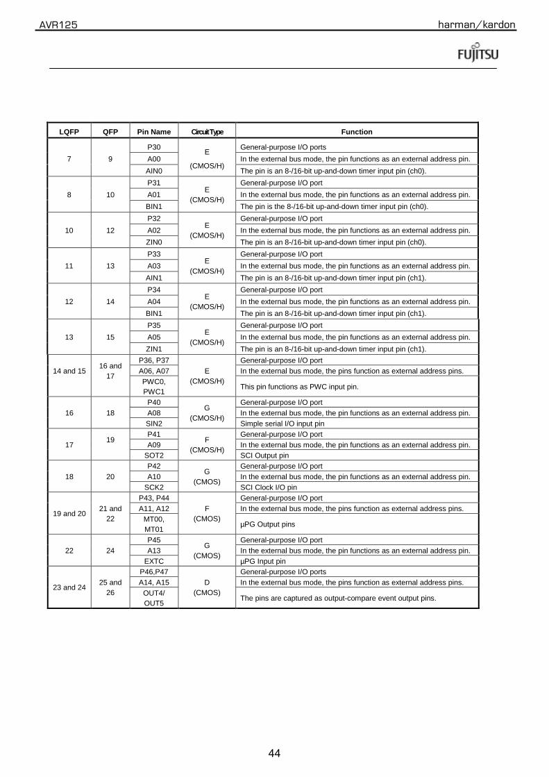
LQFP QFP Pin Name Circuit Type Function
P30 General-purpose I/O ports
A00 In the external bus mode, the pin functions as an external address pin.7 9
AIN0
E
(CMOS/H)The pin is an 8-/16-bit up-and-down timer input pin (ch0).
P31 General-purpose I/O port
A01 In the external bus mode, the pin functions as an external address pin.8 10
BIN1
E(CMOS/H)
The pin is the 8-/16-bit up-and-down timer input pin (ch0).
P32 General-purpose I/O port
A02 In the external bus mode, the pin functions as an external address pin.10 12
ZIN0
E(CMOS/H)
The pin is an 8-/16-bit up-and-down timer input pin (ch0).
P33 General-purpose I/O port
A03 In the external bus mode, the pin functions as an external address pin.11 13
AIN1
E(CMOS/H)
The pin is an 8-/16-bit up-and-down timer input pin (ch1).
P34 General-purpose I/O port
A04 In the external bus mode, the pin functions as an external address pin.12 14
BIN1
E(CMOS/H)
The pin is an 8-/16-bit up-and-down timer input pin (ch1).
P35 General-purpose I/O port
A05 In the external bus mode, the pin functions as an external address pin.13 15
ZIN1
E(CMOS/H)
The pin is an 8-/16-bit up-and-down timer input pin (ch1).
P36, P37 General-purpose I/O portA06, A07 In the external bus mode, the pins function as external address pins.14 and 15
16 and17
PWC0,PWC1
E(CMOS/H)
This pin functions as PWC input pin.
P40 General-purpose I/O portA08 In the external bus mode, the pin functions as an external address pin.16 18SIN2
G(CMOS/H)
Simple serial I/O input pinP41 General-purpose I/O portA09 In the external bus mode, the pin functions as an external address pin.17
19
SOT2
F(CMOS/H)
SCI Output pinP42 General-purpose I/O portA10 In the external bus mode, the pin functions as an external address pin.18 20
SCK2
G(CMOS)
SCI Clock I/O pinP43, P44 General-purpose I/O portA11, A12 In the external bus mode, the pins function as external address pins.
19 and 2021 and
22 MT00,MT01
F(CMOS)
µPG Output pins
P45 General-purpose I/O portA13 In the external bus mode, the pin functions as an external address pin.22 24
EXTC
G(CMOS)
µPG Input pinP46,P47 General-purpose I/O portsA14, A15 In the external bus mode, the pins function as external address pins.
23 and 2425 and
26 OUT4/OUT5
D(CMOS)
The pins are captured as output-compare event output pins.
44
AVR125 harman/kardon

LQFP QFP Pin Name Circuit Type Function
P50General-purpose I/O portIn the external bus mode, the pin functions as ALE pin.
68 70ALE
D(CMOS) In the external bus mode, the pin functions as an address capture
enable signal (ALE) pin.
P51General-purpose I/O portIn the external bus mode, the pin functions as the RDX pin.
69 71RDX
D(CMOS) When the external bus mode is enabled, the pin functions as the read
strobe output (RDX) pin.
P52General-purpose I/O portWhen the external bus mode is enabled and the WRE bit of the EPCRregister is 1, the pin functions as the WRLX pin
70 72
WRLX
D(CMOS) When the external bus mode is enabled, the pin functions as the lower-
order side data write strobe output (WRLX) pin. When the WRE bit ofthe EPCR register is 0, the pin functions as a general-purpose I/O port.
P53
General-purpose I/O portWhen the external bus mode is enabled (the bus is 16-bits long) andthe WRE bit of the EPCR register is 1, the pin functions as the WRHXpin.
71 73
WRHX
D(CMOS) When the external bus mode is enabled (the bus is 16-bits long), the
pin functions as the higher-order side data write strobe output (WRHX)pin. When the WRE bit of the EPCR register is 0, the pin functions asa general-purpose I/O port.
P54General-purpose I/O portWhen the external bus mode is enabled and the HDE bit of the EPCRregister is 1, the pin functions as the HRQ pin.
72 74
HRQ
D(CMOS) When the external bus mode is enabled, the pin functions as the hold
request input (HRQ) pin. When the HDE bit of the EPCR register is 0,the pin functions as a general-purpose I/O port.
P55General-purpose I/O portWhen the external bus mode is enabled and the HDE bit of the EPCRregister is 1, the pin functions as the HAKX pin.
73 75
HAKX
D(CMOS) When the external bus mode is enabled, the pin functions as the hold
acknowledge output (HAKX) pin. When the HDE bit of the EPCRregister is 0, the pin functions as a general-purpose I/O port.
P56General-purpose I/O port When the external bus mode is enabled andthe RYE bit of the EPCR register is 1, the pin functions as the RDY pin.
74 76RDY
D(CMOS)
When the external bus mode is enabled, the pin functions as theexternal ready input (RDY) pin. When the RYE bit of the EPCRregister is 0, the pin functions as a general-purpose I/O port.
P57General-purpose I/O port When the external bus mode is enabled andthe CKE bit of the EPCR register is 1, the pin functions as the CLK pin.
76 78CLK
D(CMOS)
When the external bus mode is enabled, the pin functions as themachine cycle clock output (CLK) pin. When the CKE bit of the EPCRregister is 0, the pin functions as a general-purpose I/O port.
P60 to P63 General-purpose I/O port36 to 39 38 to 41 AN0 to
AN3
H(CMOS) The pins function as analog input pins.
P64 to P67 General-purpose I/O port41 to 44 43 to 46 AN4 to
AN7
H(CMOS) The pins function as analog input pins.
P70 General-purpose I/O port25 27
SIN0G
(CMOS/H) The pin functions as an UART data input pin.
45
AVR125 harman/kardon

LQFP QFP Pin Name Circuit Type Function
P71 General-purpose I/O port26 28
SOT0F
(CMOS) The pin functions as an UART data output pin.P72 General-purpose I/O port
27 29SCK0
G(CMOS/H) The pin functions as an UART clock I/O pin.
P73 General-purpose I/O port28 30
TIN0G
(CMOS/H) The pin functions as the event input pin of the 16-bit reload timer.P74 General-purpose I/O port
29 31TOT0
F(CMOS/H) The pin functions as the output pin of the 16-bit reload timer.
P75 General-purpose I/O port30 32
PWC2G
(CMOS/H) The pin functions as a PWC input pin.P76 General-purpose I/O port
3133
SCLI
(NMOS/H)The pin functions as the I2C interface data I/O pin.While the I2C interface is operating, set the port output to Hi-Z.
P77 General-purpose I/O port32 34
SDAI
(NMOS/H)The pin functions as the I2C interface clock I/O pin.While the I2C interface is operating, set the port output to Hi-Z.
P80, P81 General-purpose I/O port4546
4748 IRQ0, IRQ1
E(CMOS/H) The pins function as external interrupt input pins.
P82 to P87 General-purpose I/O port50 to 55 52 to 57
IRQ2 to IRQ7E
(CMOS/H) The pins function as external interrupt input pins.P90 General-purpose I/O portSIN1 The pin functions as the simple serial I/O data input pin.56 58CS0
E(CMOS/H)
Chip select 0P91 General-purpose I/O port
SOT1 The pin functions as the I/O clock I/O pins.57 59CS1
D(CMOS)
Chip Select 1P92 General-purpose I/O port
SCK1 The pin functions as the SCI clock I/O pin.58 60CS2
E(CMOS/H)
Chip Select 2P93 General-purpose I/O port
FRCKThe pin functions as the external clock input pin while the free-runningtimer is in use.
ADTGThe pin functions as the external trigger input pin while the A/Dconverter is in use.
59 61
CS3
E(CMOS/H)
Chip Select 3P94 General-purpose I/O port
60 62PPG4
D(CMOS/H) The pin functions as a PPG timer output pin.
P95 General-purpose I/O port61 63
PPG5D
(CMOS) The pin functions as a PPG timer output pin.P96 General-purpose I/O port
62 64IN0
E(CMOS/H) The pin is captured as the input capture ch0 trigger input pin.
P97 General-purpose I/O port63 65
IN1E
(CMOS/H) The pin is captured as the input capture ch1 trigger input pin.PA0 to PA3 General-purpose I/O port
64 to 67 66 to 69OUT0 to OUT3
D(CMOS) The pins are captured as the output-compare event output pins.
33 35 AVCC - Pin for power supply to A/D converter34 36 AVRH - Pin for external reference power supply to A/D converter35 37 AVSS - Pin for power supply to A/D converter
47 to 49 49 to 51 MD0 to MD2J
(CMOS/H)Input pins for selecting operation mode
82 84 VCC3 - Pin for power supply 3.3 V ± 0.3 V (VCC3)21 23 VCC5 - Amphibious pin for power supply 3.3 V ± 0.3 V/5.0 V ± 0.5 (VCC5)9
4079
114281
VSS - Pins for input for power (GND)
46
AVR125 harman/kardon

47
AVR125 harman/kardon
최동찬
NJM2068M : IC23~29 , 32~34 , 82,88

S5
S1S2
6.2dBAmp
75dirver
6.2dBAmp
6.2dBAmp
S4
S3
S6
S720K
20K
20K13Vin1
V+
V-
SW2 SW1
Vout1
Vout2
Vout3
SW4
BLOCK DIAGAM (NJM2296M ) : IC41, 43, 44
SW3GND
SW5
Vin2
Vin3
Vin4
Vin5
1
15
11
16 10 14
12
2
9
7
5
4 6 8
3
20K
20K
20K
20K
20K
75dirver
75dirver
48
AVR125 harman/kardon

49
AVR125 harman/kardon
최동찬
NJM4556AM : IC86

LEV
EL
SH
IFT
ER
21
2
3
4
1
5
6
2
7
8
3
1
2
3
4
1
5
6
2
7
8
3
1
3
4
5
6
7
8
9
10
14 28
11
12
13
27
26
25
24
23
22
21
20
19
18
17
16
15
LAT
CH
CIR
CU
IT
SHIFT REGISTER
LEV
EL
SH
IFT
ER
LAT
CH
CIR
CU
IT
L-S R-S
Vss GND VDD
L-S
L-S
L-S
L-COM
L-S
L-S
L-COM
L-S
L-S
L-COM
ST
R-S
R-S
R-S
R-COM
R-S
R-S
R-COM
R-S
R-S
R-COM
DATA
CK
LEV
EL
SH
IFT
ER
21
2
3
1
4
5
6
2
7
8
3
1
2
3
1
4
5
6
2
7
8
3
1
3
4
5
6
7
8
9
10
14 28
11
12
13
27
26
25
24
23
22
21
20
19
18
17
16
15
LAT
CH
CIR
CU
IT
SHIFT REGISTER
LEV
EL
SH
IFT
ER
LAT
CH
CIR
CU
IT
L-S R-S
Vss GND VDD
L-S
L-S
L-COM
L-S
L-S
L-S
L-COM
L-S
L-S
L-COM
ST
R-S
R-S
R-COM
R-S
R-S
R-S
R-COM
R-S
R-S
R-COM
DATA
CK
TC9164AF (FUNCTION/INPUT) : IC22
BLOCK DIAGRAM
TC9163AF (FUNCTION/INPUT) : IC20
BLOCK DIAGRAM
50
AVR125 harman/kardon

1dBVR
latch
8dBVR
latch
1dBVR
latch
8dBVR
latch
3 to 7decoder
4 to 13decoder
1dBVR
latch
Shift register (32BIT) Strobe generatecircuit
Level shift circuit
8dBVR
latch
2
3L-OUTA
NC VSS VDD TEST
L-INA 4
5L-A-GNDA
L-OUTB 6
L-INB 7
8L-A-GNDB
L-OUTC 9
L-INC 10
12CS1
GND 13
CK 14
L-A-GNDC 11
3 L-OUTA
L-INA4
5 L-A-GNDA
L-OUTB
Same as L-chCircuit
6
L-INB7
8 L-A-GNDB
L-OUTC9
L-INC10
12 CS1
GND13
CK14
L-A-GNDC11
1 28 27
TC9482F (ELECTRONIC VOLUME/INPUT) : IC31
TC9215AF (TONE CONTROL : IC80)
BLOCK DIAGRAM
GND 1
TC9215AF
OFF 2
3S10
S11
S12
S20
S21
S41
S40
S42
S34
S32
S31
S30 Vss
DD
4
5
6
7
16 V
15
14
13
12
11
10
8 9
51
AVR125 harman/kardon

TRANSISTOR, REGULATOR IC BLOCK DIAGRAM
TO-92M
1. Emitter2. Collector3. Base
1. Emitter2. Collector3. Base
KTC2874BKRA107M
2SA1360OKTD600KG
KTD1302TKTC3200GRKTA1271Y
KTA1268GRKTC3198Y
KSC2785YKRC107M
2SC3423O
1. Emitter2. Collector3. Base
TO-126
TO-92
123 123
123
1. Base2. Collector3. Emitter
KSA614Y
TO-220
123
1. INPUT2. GND3. OUTPUT
MC7815C MC7805C
TO-220
123
1. GND2. INPUT3. OUTPUT
MCNJM7905 MC7915C
TO-220
123
1. Base2. Collector3. Emitter
2SB1560 2SD2390
KTA1024Y KSC2316Y
1. Emitter2. Collector3. Base
TO-3P
TO-92L
123
1 2 3
52
AVR125 harman/kardon

AVR125 ELECTRICAL PARTS LIST
Reference Designator Part Number Description
PCB , FRONT
Capacitors
C703 HCBS1H821KBT CAP , CERAMIC 820PF 50V K
C712 HCEA1HH1R0T CAP , ELECT 1UF 50V
C714,775,776 HCBS1H151KBT CAP , CERAMIC 150PF 50V KC716,872,873 HCEA1CH331T CAP , ELECT 330UF 16VC719~721 HCBS1H181KBT CAP , CERAMIC 180PF 50V KC722 HCBS1H220JT CAP , CERAMIC 22PF 50V JC723,807 CCFT1H104ZF CAP , SEMI 0.1UF 50V ZFC725,729,865 CCKT1H473ZF CAP , CERAMIC 0.047UF 50V ZFC726,863,886 HCEA0JH102T CAP , ELECT 1000UF 6.3VC731 HCEA1HH100T CAP , ELECT 10UF 50VC733 HCEA1EH470T CAP , ELECT 47UF 25VC737,738 HCBS1H180JT CAP , CERAMIC 18PF 50V J
C783,784,855,856 HCBS1H101KBT CAP , CERAMIC 100PF 50V KC785,786,850,851 HCBS1H470JT CAP , CERAMIC 47PF 50V JC793,794,799,800 KCFE1J183JBT CAP , FILM 0.018UF 63V JC795,796 KCFE1J823JBT CAP , FILM 0.082UF 63V JC797,798 KCFE1J332JBT CAP , FILM 0.0033UF 63V JC808 CCKT1H181KB CAP , CERAMIC 180PF 50V KBC809 HCEA1AH471T CAP , ELECT 470UF 10VC810,811 HCEA1CH101T CAP , ELECT 100UF 16V
C813,814 HCEA1HH4R7T CAP , ELECT 4.7UF 50VC870,871 HCBS1H681KBT CAP , CERAMIC 680PF 50V KBC875~878 HCBS1H103ZFT CAP , CERAMIC 0.01UF 50V ZC880 HCEA1AH221T CAP , ELECT 220UF 10VC734,885 BCES0HD104 CAP , GOLD JP EECS0HD104VC853 KCKDKS472ME CAP , CERAMIC(X1/Y2/SC) 0.0047UF/2.5KV
Diodes
D701~703,705~716,718-722,729-754, 756-760 CVD30BSGATAAT L.E.D , GREEN (TAPPING)D761,774,775,777,779 HVD1SS133MT DIODE 1SS133T-77D776 KVD1N4003ST DIODE 1N4003D778 KVD1N4003ST DIODE 1N4003D723 CVD50BOGDWGA L.E.D , 2 COLOR
Transistors
Q734~737 HVTKTC2874BT T.R , MUTE KTC2874B
0.022UF 50V ZCAP , CERAMICHCBS1H223ZFTC713,730,732,736,770,771,805, 806,858-862
C781,782,787~790,866,867
Q701~703,705~716,718-722,724-729
C704,735,773,774,777,778,864
C779,780,791,792,868,869
C812,852,857,874, 882,883
HCEA1VH100T CAP , ELECT 10UF 35V
HCEA1CKS470T CAP, ELECT 47UF 16V
HCEA1CKS100T CAP , ELECT 10UF 16V
HCBS1H104ZFT CAP , CERAMIC 0.1UF 50V Z
HVTKRC107MT T.R KRC107M
53
AVR125 harman/kardon

Reference Designator Part Number Description
Intergrated Circuits
IC72 BVIMB90F476APFG IC , FLASH U-COM FUJITSUIC73 HRVRPM6938H4 SENSOR , REMOTE RPM6938-H4IC74 HVILC75725E IC , VFL DRIVER LC75725EIC80 HVITC9215AF I.C TC9215AFIC81,82,88 HVINJM2068MTE1 I.C , OP AMP NJM2068M-TE1IC83,84 HVI74ACT04SC I.C , HEX INVERTER 74ACT04SCIC86 HVINJM4556AMTE1 I.C , OP AMP NJM4556AM-TE1IC85 HVIRE5VT15CATZ IC , RESET RE5VT15CATZIC87 HVIRE5VL28CATZ IC , RESET RE5VL28CATZ
Resistors
R704,757,763 CRD20TJ332T RES , CARBON 3.3K OHM 1/5W JR730,833,834 CRD20TJ112T RES,CABONR731,748,849,850,913 CRD20TJ223T RES , CARBON 22K OHM 1/5W JR732,847,848,853,854 CRD20TJ222T RES , CARBON 2.2K OHM 1/5W J
R737,R892,R893 CRD20TJ100T RES , CARBON 10 OHM 1/5W J
R754,760,767,901,902 CRD20TJ152T RES , CARBON 1.5K OHM 1/5W JR755,761,768 CRD20TJ182T RES , CARBON 1.8K OHM 1/5W JR758,764,823,831,832,907,908, 918,919
R765 CRD20TJ752T RES , CARBON 7.5K OHM 1/5W JR775~800,802~806 CRD20TJ151T RES , CARBON 150 OHM 1/5W J
R824,873,874 CRD20TJ471T RES , CARBON 470 OHM 1/5W JR825 CRD20TJ181T RES , CARBON 180 OHM 1/5W JR829,830,835,836 CRD20TJ184T RES , CARBON 180K OHM 1/5W JR841,842,914~916 CRD20TJ473T RES , CARBON 47K OHM 1/5W JR843,844 CRD20TJ105T RES , CARBON 1M OHM 1/5W JR851,852 CRD20TJ392T RES , CARBON 3.9K OHM 1/5W JR855,856 CRD20TJ681T RES , CARBON 680 OHM 1/5W JR857,858,909~912 CRD20TJ221T RES , CARBON 220 OHM 1/5W JR868,894 CRD20TJ1R0T RES , CARBON 1 OHM 1/5W JR869,876~878 CRD20TJ750T RES , CARBON 75 OHM 1/5W JR875 CRD20TJ103T RES , CARBON 10K OHM 1/5W JR917 CRD20TJ123T RES , CARBON 12K OHM 1/5W JVR71 CVV2X05M104Z RES , VARIABLE(BALANCE) RK14128030214YVR72,73 CVV2X07C104Z RES , VARIABLE(TONE) RK14128030214C
Miscellaneous
S701~721 CST1A012ZT SW , TACT SKHV10910GSW01 HSH1A008ZV SW , PUSH (MOMS)BN10 CWZAVR125BN10 WIRE ASS'Y (SHIELD)BN16 CWZAVR2550BN16 WIRE ASS'Y (SHIELD)BN18 CWZAVR125BN18 WIRE ASS'Y (SHIELD)
R753,759,766,865,903,904
R813,814,839,840,845,846,871, 872,899,900,905,906
R810,811,822,837,838,895-898
R701~703,705~716,718-722,826,827
R733,736,756,762,762,769,864,866
R734,735,744~747,771-773,875,881-891
CRD20TJ121T RES , CARBON 120 OHM 1/5W J
CRD20TJ272T RES , CARBON 2.7K OHM 1/5W J
CRD20TJ103T RES , CARBON 10K OHM 1/5W J
CRD20TJ102T RES , CARBON 1K OHM 1/5W J
CRD20TJ562T RES , CARBON 5.6K OHM 1/5W J
CRD20TJ101T RES , CARBON 100 OHM 1/5W J
CRD20TJ104T RES , CARBON 100K OHM 1/5W J
54
AVR125 harman/kardon

Reference Designator Part Number Description
BN41 CWZAVR125BN41 WIRE ASS'Y (SHIELD)BN80 CWB2B908320EW WIRE ASS'YBN81 CWB2B906250BM WIRE ASS'YBN83 CWB1C902250BM WIRE ASS'YBN84 CWB2B905100EN WIRE ASS'YBN85,90 CWB2B902090EN WIRE ASS'YBN87 CWZAVR2550BN87 WIRE ASS'Y (SHIELD)BN88 CWB2B904070EN WIRE ASS'YBN89 CWB2B905080EN WIRE ASS'YBN94 KJP10GB99ZM WAFER MOLEX35237-1010BN95 KJP08GB99ZM CONNECTOR , HOUSING MOLEX35237-0810CN10 KJP04GB46ZM WAFER MOLEX 53015CN11 KJP09GA98ZM WAFER MOLEX35336-0910CN12 KJP14GA98ZM WAFER MOLEX35336-1410CN16 KJP08GB46ZM WAFER MOLEX 53015CN72 KJP32GA117ZG WAFER , CARD CABLE GF102-32S-TSCN82 KJP06HA37ZM WAFER MOLEX42140-2206CN84,89 KJP05GA19ZM WAFER MOLEX53014-0510CN85,90 KJP02GA19ZM WAFER MOLEX53014-0210CN86 KJP02GA89ZM WAFER MOLEX35328-02CN87 KJP06GA19ZM WAFER MOLEX53014-0610CN88 KJP04GA19ZM WAFER MOLEX53014-0410FIP1 HFLCM2054C F.I.P (DISPLAY)JK81 CJJ4M041Z JACK , BOARD (COAX)JK82 HJSTORX179 MODULE,OPTICAL(RECEIVE) TORX179JK83 HJJ2E026Z JACK , HEADPHONE(SIVER PLATE)JK85 CJJ9M003Z JACK , S-VIDEOJK86 CJJ4S023Z JACK , BOARDJW82 CWZAVR2550JW82 WIRE , ASS'YJW83 CWE8202150RV WIRE ASS'YJW84 CWE8202110RV WIRE, ASS'YVR74 HSR2A023Z VR , ENCODERX701 HOX04194E120C CRYSTALL702 HLQ02C100KT COIL , AXAIL
PCB , MAIN
Capacitors
C501~505 HCEA1VH100T CAP , ELECT 10UF 35VC506~510 CCKT1H331KB CAP , CERAMIC 330PF 50V KBC561~565,907 HCEA1CH101T CAP , ELECT 100UF 16VC566~570 HCEA1EH470T CAP , ELECT 47UF 25VC571~575 CCKT1H681KB CAP , CERAMIC 680PF 50V KBC601~605 CCCT1H120JC CAP , CERAMIC 12PF 50V JCC606~610 CCCT1H330JC CAP , CERAMIC 33PF 50V JCC641~645,681~685 HCEA1HH100T CAP , ELECT 10UF 50VC826 HCQI1H182JZT CAP , MYLAR 1800PF 50V JC901,998 CCFT1H104ZF CAP , SEMI 0.1UF 50V ZF
C911 HCEA1CH471T CAP , ELECT 470UF 16VC912 HCEA1CH221T CAP , ELECT 220UF 16VC922,924,962 HCEA1EH101T CAP , ELECT 100UF 25VC938,991 HCEA1HH1R0T CAP , ELECT 1UF 50VC939 HCEA1HH4R7T CAP , ELECT 4.7UF 50VC940 HCEA1AH471T CAP , ELECT 470UF 10VC971~975 HCQI1H562JZT CAP , MYLAR 5600PF 50V JC976~979,993~997 HCQI1H473JZT CAP , MYLAR 0.047UF 50V JC631~640 HCEA1JH221E CAP , ELECT 220UF 63VC903 BCQE2E104KDE CAP , LINE ACROSS 0.1UF 250V KD
C905,908,923,925,963,999 CCKT1H223ZF CAP , CERAMIC 0.022UF 50V ZF
55
AVR125 harman/kardon

Reference Designator Part Number Description
C904 KCKDKS472ME CAP , CERAMIC(X1/Y2/SC) 0.0047UF/2.5KVC906 HCEA1EH102E CAP , ELECT 1000UF 25VC915,916 HCET63VFHS123ND CAP , ELECT 12000UF 63VC917 HCEA1EH332E CAP , ELECT 3300UF 25VC918 HCEA1EH222E CAP , ELECT 2200UF 25VC961 HCEA1CH472E CAP , ELECT 4700UF 16V
Diodes
D956 KVD1N4003SRT DIODE TW 1N4003
Transistors
Q501~505,601~605 HVTKTA1268GRT T.R KTA1268GRQ511~520,556~565 HVTKTC3200GRT T.R KTC3200GRQ541~545 HVTKTC3198YT T.R KTC3198YQ611~615 HVTKTD600KGR T.R , BIAS KTD600KGRQ621~625 HVT2SA1360O T.R 2SA1360OQ626~630 HVT2SC3423O T.R 2SC3423OQ652~655,661 BVT2SB1560 T.R , POWER 2SB1560Q657~660,670 BVT2SD2390 T.R , P0WER 2SD2390Q681~685,901,942,943
Q806,969~973 HVTKTC2874BT T.R , MUTE KTC2874BQ938,939,952,992 HVTKRA107MT T.R KRA107MQ951,960,991 HVTKRC107MT T.R KRC107MQ961 HVTKTA1024YT T.R KTA1024Y
Intergrated Circuits
IC91 HVIMC7815C I.C, REGULATOR KA7815-ABTUIC92 HVIMC7915C I.C, REGULATOR KA7915-ABTUIC93,94 HVIMC7805C I.C, REGULATOR KA7805-ABTU
Resistors
R501~505 CRD20TJ433T RES , CARBON 43K OHM 1/5W JR506~510 CRD20TJ333T RES , CARBON 33K OHM 1/5W JR511~520,940 CRD20TJ152T RES , CARBON 1.5K OHM 1/5W J
R527~530,621~626 CRD20TJ750T RES , CARBON 75 OHM 1/5W JR531~540 CRD20TJ221T RES , CARBON 220 OHM 1/5W JR541~545 CRD20TJ271T RES , CARBON 270 OHM 1/5W JR556~560,962 CRD20TJ273T RES , CARBON 27K OHM 1/5W JR561~565,678~680 CRD20TJ182T RES , CARBON 1.8K OHM 1/5W J
R576~580 CRD20TJ100T RES , CARBON 10 OHM 1/5W J
R611~615,961 CRD20TJ331T RES , CARBON 330 OHM 1/5W JR616~620 CRD20TJ122T RES , CARBON 1.2K OHM 1/5W JR631~640 KRD25FJ180T RES , CARBON 18 OHM 1/4W JR646~655 KRD25FJ3R3T RES , CARBON 3.3 OHM 1/4W JR666~670,696~700 CRD25TJ470T RES , CARBON 47 OHM 1/4W J
D501~505,581~585,902,911,912, 914-916,953-955
R521~525,806,974-978
R566~575,581~600,987
R601~610,941~943,945
D901,903~906,961-963
HVD1SS133MT DIODE 1SS133T-77
KVD1N4003ST DIODE 1N4003
KVTKSC2785YT T.R KSC2785Y
CRD20TJ471T RES , CARBON 470 OHM 1/5W J
CRD20TJ561T RES , CARBON 560 OHM 1/5W J
CRD20TJ223T RES , CARBON 22K OHM 1/5W J
56
AVR125 harman/kardon

Reference Designator Part Number Description
R671~675 CRD20TJ911T RES , CARBON 910 OHM 1/5W JR676,677 CRD25TJ182T RES , CARBON 1.8K OHM 1/4W JR681~685,960,992 CRD20TJ562T RES , CARBON 5.6K OHM 1/5W J
R816,939,969~973 CRD20TJ472T RES , CARBON 4.7K OHM 1/5W JR826,979~983 CRD20TJ473T RES , CARBON 47K OHM 1/5W JR910,963 CRD20TJ105T RES , CARBON 1M OHM 1/5W JR911 CRD20TJ820T RES , CARBON 82 OHM 1/5W JR913,914 CRD20TJ153T RES , CARBON 15K OHM 1/5W JR917~920 CRD25TJ393T RES , CARBON 39K OHM 1/4W JR944 CRD25TJ223T RES , CARBON 22K OHM 1/4W JR986 CRD20TJ102T RES , CARBON 1K OHM 1/5W JR988 CRD20TJ303T RES , CARBON 30K OHM 1/5W JR991 CRD20TJ822T RES , CARBON 8.2K OHM 1/5W JR656~660 KRF5EKR22HX2 RES , CEMENT(*2) 0.22/5W *2R904 BRDERC12UGK335T RES , CARBON JP 3.3M OHM 1/2WR905,993~997 KRG1ANJ100H RES , METAL OXIDE FILM 10 OHM 1W JVR61~65 HVN1RA221B01T RES , SEMI FIXED(220 OHM) RH0615C100221
Miscellaneous
BN20 CWB3FB03280UP WIRE ASS'YBN90 CWB4D232450PU WIRE ASS'YJW91 CWE8212230VV WIRE ASS'YJW92 CWEE212120VV WIRE ASS'YCN61~65 KJP03GA01ZM WAFER MOLEX 5267-03ACN80 KJP08GA19ZM WAFER MOLEX53014-0810CN91 KJP02KA060ZY WAFER 7.92MM(YUNHO)CN92 KJP02GA89ZM WAFER MOLEX35328-02CN94 KJP10GA98ZM WAFER MOLEX35336-1010CN95 KJP08GA98ZM WAFER MOLEX35336-0810CN96 KJP07GA01ZM WAFER MOLEX 5267-07AJK91 CJJ5N009Z TERMINAL , SPEAKERJK92 CJJ5Q011Z TERMINAL , SPEAKERJK93 CJJ4M040Z JACK , BOARD (SW)L501~505 CLEY0R5KAK COIL , SPEAKER 0.5UH KOL91 KJJ7A015Z OUTLET , AC(UL/2P/SEP) A204D0041PRY94 HSL1A008ZE RELAY SDT-S-112DMRTH91 KRTP42T7D330B THERMAL SENSOR , POSISTOR P42T7D330BW20T902 CLT5J033ZU TRANS , SUB SR-68
PCB , INPUT
Capacitors
C238,239,335,360 CCKT1H471KB CAP , CERAMIC 470PF 50V KBC261~272 HCEA1EH220T CAP , ELECT 22UF 50VC273~284 HCQI1H332JZT CAP , MYLAR 3300PF 50V J
C287,293,371 HCQI1H182JZT CAP , MYLAR 1800PF 50V J
R686~690,930,932,966,998
C201~206,211~224,321,322,325,326
C231~236,349,350,799,382~386,390, 421,426,440,447,452,454,456,708,709, 712,728,731,733,752,754,780,783
C237,240,359,361,362,387,703,705
C285,286,288~292,294-296,333
CCKT1H181KB 180PF 50V KB
CCKT1H561KB CAP , CERAMIC 560PF 50V KB
CAP , CERAMIC
CCKT1H221KB CAP , CERAMIC 220PF 50V KB
HCEA1CH101T CAP , ELECT 100UF 16V
CRD20TJ103T RES , CARBON 10K OHM 1/5W J
57
AVR125 harman/kardon

Reference Designator Part Number Description
C303~308 HCEA1HH220T CAP , ELECT 22UF 50VC336,357,461,735,921 CCKT1H223ZF CAP , CERAMIC 0.022UF 50V ZFC339,340,772 HCBS1H103ZFT CAP , CERAMIC 0.01UF 50V Z
C372~374 CCKT1H151KB CAP , CERAMIC 150PF 50V KBC388,389 HCEA1CH471T CAP , ELECT
C395 HCEA1HH1R0T CAP , ELECT 1UF 50V
C457,721,737 HCBS1H101KBT CAP , CERAMIC 100PF 50V KC701,702,781,784 HCEA1AH471T CAP , ELECT 470UF 10V
C710,778,785 CCKT1H473ZF CAP , CERAMIC 0.047UF 50V ZFC711,713,714,716~718 CCCT1H270JC CAP , CERAMIC 22PF 50V JCC715,782 HCBS1H473ZFT CAP , CERAMIC 0.047UF 50V ZC722,723 CCCT1H100DC CAP , CERAMIC 10PF 50V DCC724 HCBS1H330JT CAP , CERAMICC725 CCCT1H330JC CAP , CERAMIC 33PF 50V JCC392,741,742 HCEA1EH470T CAP , ELECT 47UF 25VC745,770 HCEA1HH2R2T CAP , ELECT 2.2UF 50VC764,765 CCCT1H120JC CAP , CERAMIC 12PF 50V JCC771 HCBS1H471KBT CAP , CERAMIC 470PF 50V KBC775 CCKT1H102KB CAP , CERAMIC 1000PF 50V KBC777 HCEA0JH102T CAP , ELECT 1000UF 6.3VC903~906,908,910,913 CCKT1H103ZF CAP , CERAMIC 0.01UF 50V ZFC907,909,914 HCEA1HH470T CAP , ELECT 47UF 50VC911 HCEA1HH4R7T CAP , ELECT 4.7UF 50VC912 HCEA1HH101T CAP , ELECT 100UF 50VC915,916 HCQI1H104JZT CAP , MYLAR 0.1UF 50V JC917,918 HCQI1H103JZT CAP , MYLAR 0.01UF 50V JC919,920 HCQI1H473JZT CAP , MYLAR 0.047UF 50V JC922 HCEA1EH101T CAP , ELECT 100UF 25VC923 HCEA1CH332E CAP , ELECT 3300UF 16V
Diodes
D418 HVDMTZJ5.6BT DIODE , ZENER 5.6V 1/2WD701 HVDMTZJ4.7BT DIODE , ZENER 4.7V 1/2WD702 HVDMTZJ3.3BT DIODE , ZENER 3.3V 1/2WD901~906 KVD1N4003SRT DIODE TW 1N4003D907,910 HVDMTZJ15BT DIODE , ZENER 15V 1/2WD908 HVDMTZJ6.2BT DIODE , ZENER 6.2V 1/2WD909 HVDKBU804F DIODE , BRIDGE KBU804F
Transistors
Q301 HVTKTD1302T T.R KTD1302
C393,704,706,707,734,755,756,761,773, 774,901,902
C297~302,323,324,327,328,334,347, 348,358,420,430,439,446,449,460, 730,766
C343~346,351~356,363~368,375~380, 412,416,419,425,433,435,438,441,443, 445,448,453,455,762,769
C391,719,720,727,729,732,736,740,743, 744,746,747,751,763,768,779,786,787
C418,431,442,444,458,726,776
HCBS1H104ZFT CAP , CERAMIC 0.1UF 50V Z
CAP , CERAMIC 100PF 50V KBCCKT1H101KB
CCFT1H104ZF CAP , SEMI 0.1UF 50V ZF
0.022UF 50V ZHCBS1H223ZFT CAP , CERAMIC
HCEA1VH100T CAP , ELECT 10UF 35V
58
AVR125 harman/kardon

Reference Designator Part Number Description
Q302,902 HVTKRA107MT T.R KRA107MQ395,396 HVTKTC2874BT T.R , MUTE KTC2874BQ701,702 HVTKSC2316YT T.R KSC2316YQ901,903 HVTKTA1271YT T.R KTA1271YQ904 HVTKRC107MT T.R KRC107MQ455 HVTKSA614Y T.R KSA614Y
Intergrated Circuits
IC20 HVITC9163AF I.C , FUNCTION TC9163AFIC21,23~29,32~34 HVINJM2068MTE1 I.C , OP AMP NJM2068M-TE1IC22 HVITC9164AF I.C , FUNCTION TC9164AFIC30 HVITC9162AF I.C , FUNCTION TC9162AFIC31 HVITC9482F I.C , ELECT VOL TC9482FIC41,43,44 HVINJM2296M I.C , VIDEO SW NJM2296MIC71,72 HVITC74HCU04AFN IC , INVERTER TC74HCU04AFNIC75 HVIAK4114VQ IC , DIR AK4114VQIC77 HVIAK5380VT I.C 2CH AUDIO ADC AK5380VTIC78 HVIAK4356VQ I.C , D/A CONVERTER AK4356VQIC79 HVICS493263-CLG I.C , DSP HK CS493263-CLGIC95 HC3990509F I.C, REGULATOR NJM7905FA
Resistors
R224 CRD20TJ272T RES , CARBON 2.7K OHM 1/5W JR225~230,235~247 CRD20TJ474T RES , CARBON 470K OHM 1/5W J
R271~274,277~282 CRD20TJ392T RES , CARBONR275,276,413,414,421427,432,445,446450~452,458,461,463465,468,729,752,914
R289~294,301~306,908 CRD20TJ122T RES , CARBON 1.2K OHM 1/5W J
R336 CRD20TJ123T RES , CARBON 12K OHM 1/5W JR337,911 CRD20TJ153T RES , CARBON 15K OHM 1/5W JR341,395,723 CRD20TJ105T RES , CARBON 1M OHM 1/5W JR349,350 CRD20TJ151T RES , CARBON 150 OHM 1/5W JR363 CRD25TJ101T RES , CARBON 100 OHM 1/4W JR368,370,380~382,388 CRD20TJ683T RES , CARBON 68K OHM 1/5W J
R391~394 CRD20TJ112T RES,CABON 1.1K OHM 1/5W J
R313~318,713,714,716~719
R321~328,333~335,426,440,460,462, 472,475,750,751,765,767
R248,373,701,704,748,754~762,766,773
R262,263,353~358,365~367,377~379
R256~261,359~362,364,369,746,747
R283~288,295~300,340,343~346, 374~376,396,397
R250~255,307~312,329~332,338,339, 347,348,351,352,371,389,383~387,708, 712,715,726,749,753,769
CRD20TJ471TR201~206,211~223,477,720,771
CRD20TJ101T RES , CARBON 100 OHM 1/5W J
CRD20TJ102T RES , CARBON 1K OHM 1/5W J
CRD20TJ103T
CRD20TJ332T RES , CARBON 3.3K OHM 1/5W J
CRD20TJ472T RES , CARBON 4.7K OHM 1/5W J
CRD20TJ562T RES , CARBON 5.6K OHM 1/5W J
CRD20TJ104T
RES , CARBON 10K OHM 1/5W J
RES , CARBON 100K OHM 1/5W J
CRD20TJ184T RES , CARBON 180K OHM 1/5W J
470 OHM 1/5W JRES , CARBON
59
AVR125 harman/kardon

Reference Designator Part Number Description
R433,466,469,906 CRD20TJ100T RES , CARBON 10 OHM 1/5W JR725 CRD20TJ183T RES , CARBON 18K OHM 1/5W JR727,728,772 CRD20TJ4R7T RES , CARBON 4.7 OHM 1/5W JR730 CRD20TJ121T RES , CARBON 120 OHM 1/5W JR737 CRD25TJ2R7T RES , CARBON 2.7 OHM 1/4W JR740~745,764,768,777 CRD20TJ330T RES , CARBON 33 OHM 1/5W JR763 CRD20TJ333T RES , CARBON 33K OHM 1/5W JR770 CRD20TJ182T RES , CARBON 1.8K OHM 1/5W JR776 CRD25TJ1R0T RES , CARBON 1 OHM 1/4W JR778,905,907 CRD20TJ8R2T RES , CARBON 8.2 OHM 1/5W JR909,913 CRD20TJ473T RES , CARBON 47K OHM 1/5W JR912 CRD20TJ154T RES , CARBON 150K OHM 1/5W JR319 KRG2ANJ470H RES , METAL OXIDE FILM 47 OHM 2W JR901~904 KRQ1AJR47H RES , FUSE 0.47 OHM 1W J
Miscellaneous
BN21 CWB1E908060MM WIRE ASS'YBN96 CWB1C907200BM WIRE ASS'YBN97 CWB1C903080BM WIRE ASS'YJW21,22 CWE6202070AA WIRE ASS'YJW23 CWE7202110AA WIRE ASS'YJW24 CWED202100RV WIRE ASS'YJW71 CWE7202090AA WIRE ASS'YBN11 KJP09GB99ZM CONNECTOR MOLEX35237-0910BN12 KJP14GB99ZM WAFER MOLEX35237-1410CN13 KJP13GA115ZG WAFER, CARD CABLE GF120-13S-TSCN15,43 KJP09GA115ZG WAFER , CARDCABLECN18 KJP05GA19ZM WAFERCN20 KJP03GA90ZM WAFER MOLEX35313-0310CN41 KJP06GA19ZM WAFERCN72 KJP32GA117ZG WAFER , CARD CABLE GF102-32S-TSCN81 KJP06GA01ZM WAFER MOLEX 5267-06ACN83 KJP02GA01ZM WAFER MOLEX 5267-02ACN97 KJP03GA01ZM WAFER MOLEX 5267-03AL705 KLQ100J405T COIL, PEAKING(RADIAL) 10UH J 4X5L703,706,707,709 KLZ9H001Z BEAD , COREJK21 CJJ4R019Z JACK , IN/OUTJK23,24 CJJ4P014Y JACK , IN/OUTJK25 CJJ4R034Z JACK , IN/OUTJK26,27 HJSTORX179 MODULE,OPTICAL(RECEIVE) TORX179JK28 HJS9L001Z MODULE, OPTICAL TOTX178JK29 CJJ4S022Z JACK , BOARDJK42 HJJ9N001Z JACK , S-VIDEO(2P/H) JY-5036-040JK43 HJJ9S001Z JACK , S-VIDEO(3P/H) JY-5041-040JK49 CJJ4N043Z JACK , BOARDJK50 CJJ4S010Z JACK , BOARDX701 HOX12288E320C CRYSTALF900,901 KBA2C2500TLU FUSE (2.5A 250V)F902 KBA2C6300TLU FUSE (6.3A 250V)F903,904 KBA2C8000TLU FUSE (8A 250V)CB13 CWC1C4A13B080B CABLE , CARDCB15 CWC1C4A09B130B CABLE , CARD
R422,455,459,702,703,710,711,722,724, 736,774,775
R419,425,431,436,437,453,454,456,457, 464,467,470,471,473,474,705~707,709
CRD20TJ1R0T RES , CARBON 1 OHM 1/5W J
CRD20TJ750T RES , CARBON 75 OHM 1/5W J
60
AVR125 harman/kardon

Reference Designator Part Number Description
CB72 CWC1B2A32A210B CABLE , CARD
CHASSIS MISCELLANEOUS
T901 CLT5V030ZU TRANS , POWERTUNER MODULE CNVKSTM9014MS07 TUNER MODULE KSTM9014MS07
CLZ9W003Z FERRITE , RING
61
AVR125 harman/kardon
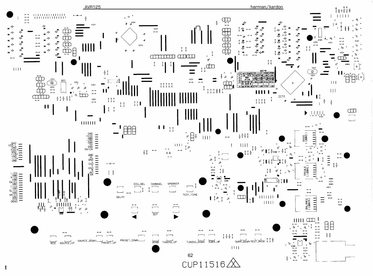
62
AVR125 harman/kardon

63
AVR125 harman/kardon

64
AVR125 harman/kardon

65
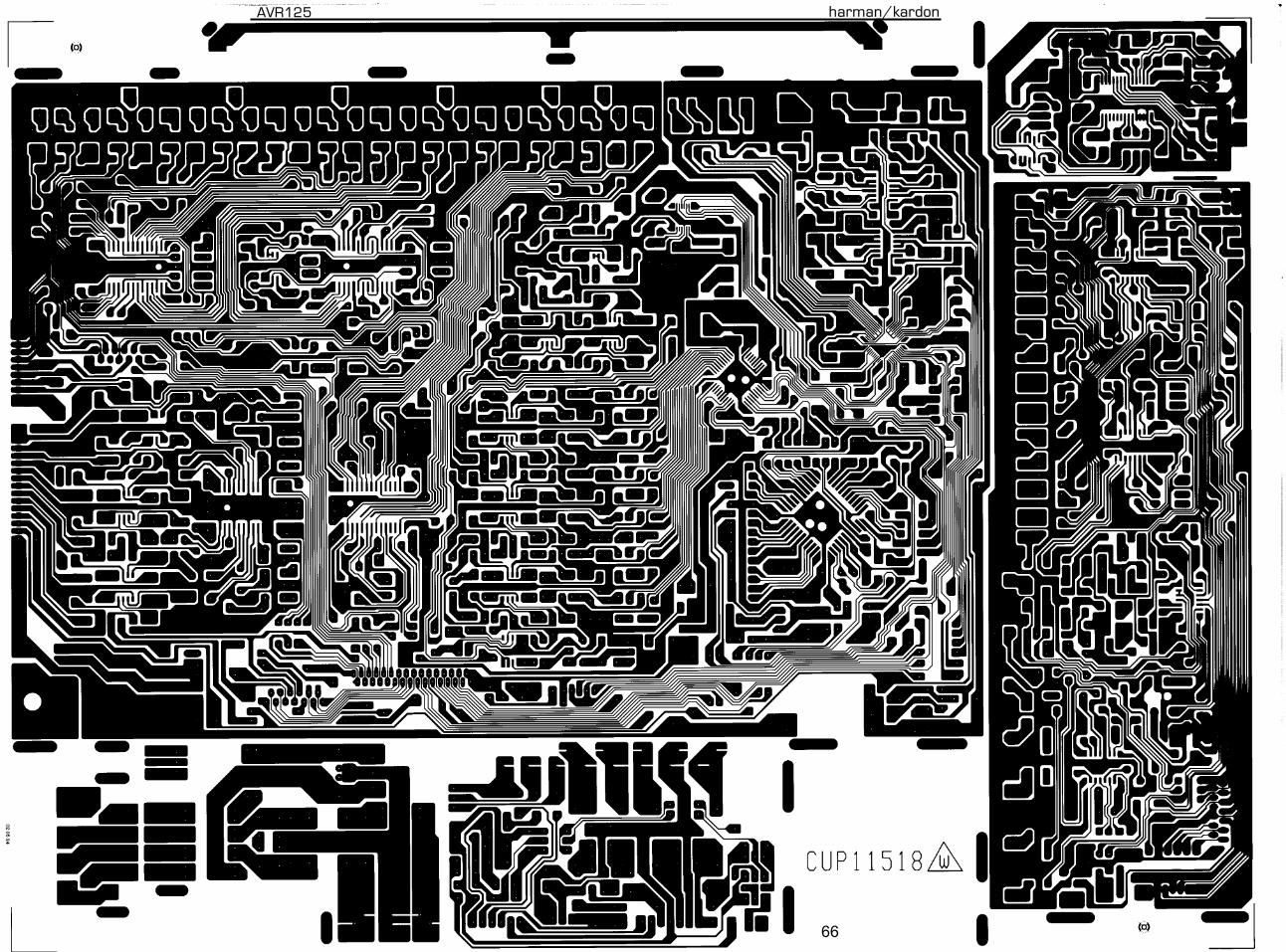
66
AVR125 harman/kardon
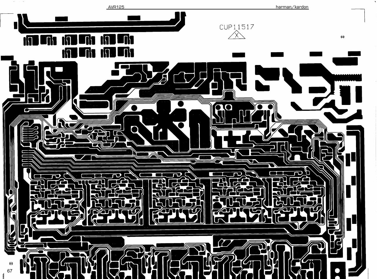
67
AVR125 harman/kardon

68

69
AVR125 harman/kardon

70

71
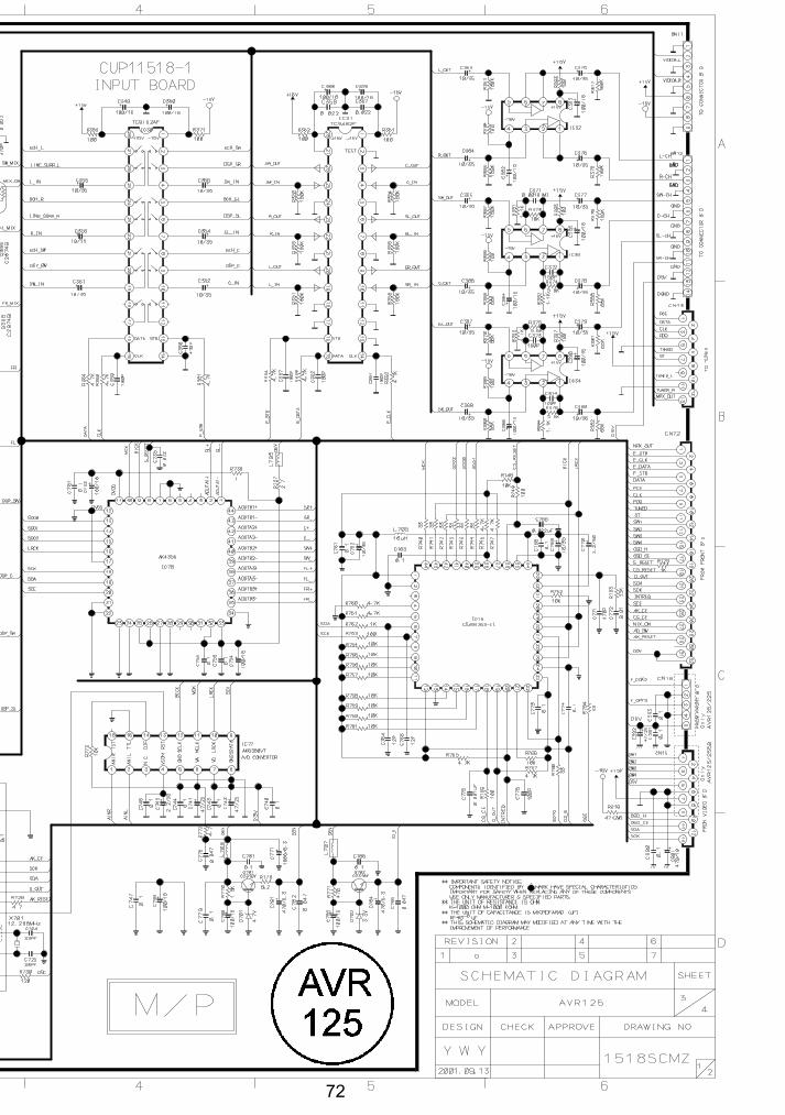
72

73

74
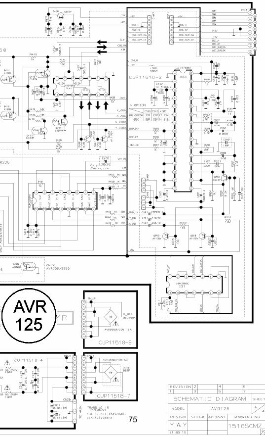
75

76

77

78

79

80

81

82

POLY BAG MANUAL INSTRUCTION
BATTERY ASS'YAM LOOP ANTENNA ASS'Y
NO DESCRIPTION PARTS NO. Q,ty
1
2
3
4
5
6
7
1
1
1
CPB1061YPOLY BAG
CQE1A169ZIMPORTANT SAFETY INSTRUCTION
CELLO OPP TAPE
MANUAL ASS'Y
BOX,OUT CARTON
4
5
1
2
DESCRIPTIONNO
CPS4A564
K4FC500CL
CQXAVR125CC
CPG1A677X
1
0.8M
1
1
Q,tyPARTS NO.
CPS4A565SNOW,PAD(R)3 1
1. Instruction manual ass'y - Accessories 2. Package Drawing
SHEET GUIDE
STAPLE10
9
8
KPL0905
CQE1A188Z
3
1
1
TAPE OPP5TAPE OPP5
MANUAL ASS'Y2
SNOW PAD (R)3
BOX ,OUT CARTON1
SET6
SNOW PAD (L)4
FM 1 POLE ANT(UL)
TRANSMITTER ASS'YREMOCON
SHEET GUIDELIMITED WARRANTY
CARDINSTRUCTION
IMPORTANT SAFETY
STAPLE
2 3
4 5 6
7 8 9
10
HARTAVR125CC
CSA1A019Z
HABAAAM1.5V
CSA3A012Z
FM 1 POL ANT(UL)
REMOCON TRANSMITTER ASS'Y
AM LOOP ANTENNA ASS'Y
BATTERY
1
1
3
1
INSTRUCTION MANUAL CQX1A778Z 1
LIMITED WARRANTY CARD CQE1A172Y 1
SNOW,PAD(L)
5 SET AVR125CCSET 1
AVR125
83
AVR125 harman/kardon