
DC1811B-A – LTM4676 Dual Step-Down µModule Regulator with ...
Upload
hoangkhanhCategory
view
230download
1
VOL 6
Automotive & TransportationSolutionsHigh Performance Analog ICs

Contents
Automotive Electronics Systems
Introduction
Automotive Quality and Reliability . . . . . . . . . . . . . . . . . . . . . . . . . . . . . . 1
Power Management
LT8672: Active Rectifier Controller . . . . . . . . . . . . . . . . . . . . . . . . . . . . 2
Surge Stoppers . . . . . . . . . . . . . . . . . . . . . . . . . . . . . . . . . . . . . . . . . . 3
Ideal Diode Controllers . . . . . . . . . . . . . . . . . . . . . . . . . . . . . . . . . . . . 3
Silent Switcher—Ultralow EMI Synchronous Switching Regulators . . . 4
60V+, High Efficiency Monolithic Step-Down DC/DC Converters . . . . . 6
40V, Ultralow Quiescent Current Monolithic Switching Regulators . . . . 8
60VIN to 150VIN Max Input DC/DC Controllers . . . . . . . . . . . . . . . . . . 10
40V, Step-Down DC/DC Converters with Cable Drop Compensation for USB Applications . . . . . . . . . . . . . . . . . . . . . . . 11
36VIN to 65VIN Max Multi-Output Step-Down DC/DC Converters . . . 12
36VIN to 40VIN Max Input Low Quiescent Current Synchronous DC/DC Controllers . . . . . . . . . . . . . . . . . . . . . . . . . . . . . 14
High Voltage Power Managers and Battery Chargers . . . . . . . . . . . . 15
High Voltage Charge Pumps . . . . . . . . . . . . . . . . . . . . . . . . . . . . . . . 16
Low Voltage (>6V) Point-of-Load Synchronous Step-Down Switching Regulators . . . . . . . . . . . . . . . . . . . . . . . . . 18
36VIN to 80VIN Max Synchronous Buck-Boost Switching Regulators . . . . . . . . . . . . . . . . . . . . . . . . . . . . . . . . . . . . . . . . . . 20
Monolithic Step-Up DC/DC Converters . . . . . . . . . . . . . . . . . . . . . . . 21
Low Noise LDOs . . . . . . . . . . . . . . . . . . . . . . . . . . . . . . . . . . . . . . . . 22
Small Solutions with µModule Regulators . . . . . . . . . . . . . . . . . . . . . 24
Small Solution Size . . . . . . . . . . . . . . . . . . . . . . . . . . . . . . . . . . . . . . 25
Low EMI µModule Regulators . . . . . . . . . . . . . . . . . . . . . . . . . . . . . . 26
Buck-Boost µModule Regulators . . . . . . . . . . . . . . . . . . . . . . . . . . . . 28
Powering FPGAs and Processors . . . . . . . . . . . . . . . . . . . . . . . . . . . 29
Battery Management
Battery Meter for Electric and Hybrid/Electric Vehicles . . . . . . . . . . . . 30
Wireless BMS Architecture . . . . . . . . . . . . . . . . . . . . . . . . . . . . . . . . 31
Measurement and Communications . . . . . . . . . . . . . . . . . . . . . . . . . 32
High Voltage Multicell Battery Stack Monitors . . . . . . . . . . . . . . . . . . 32
Active Battery Balancing ICs . . . . . . . . . . . . . . . . . . . . . . . . . . . . . . . 33
LEDs
High Efficiency LED Drivers . . . . . . . . . . . . . . . . . . . . . . . . . . . . . . . . 34
LT3965: 8-Switch Matrix LED Dimmer . . . . . . . . . . . . . . . . . . . . . . . . 36
LTM8005: µModule LED Driver . . . . . . . . . . . . . . . . . . . . . . . . . . . . . 37
Data Communications
PoDL . . . . . . . . . . . . . . . . . . . . . . . . . . . . . . . . . . . . . . . . . . . . . . . . . 38
CAN Transceivers . . . . . . . . . . . . . . . . . . . . . . . . . . . . . . . . . . . . . . . 40
isoSPI . . . . . . . . . . . . . . . . . . . . . . . . . . . . . . . . . . . . . . . . . . . . . . . . 40
SmartMesh®—Embedded Wireless Sensor Networking . . . . . . . . . . 41
Signal Chain
Radar and Lidar . . . . . . . . . . . . . . . . . . . . . . . . . . . . . . . . . . . . . . . . 42
PLL Synthesizers . . . . . . . . . . . . . . . . . . . . . . . . . . . . . . . . . . . . . . . . 42
Current Sense Amplifiers . . . . . . . . . . . . . . . . . . . . . . . . . . . . . . . . . . 43
TimerBlox® Products . . . . . . . . . . . . . . . . . . . . . . . . . . . . . . . . . . . . 44
Silicon Oscillators . . . . . . . . . . . . . . . . . . . . . . . . . . . . . . . . . . . . . . . 45
Precision Operational Amplifiers . . . . . . . . . . . . . . . . . . . . . . . . . . . . 46
Programmable Gain and Gain Selectable Amplifiers . . . . . . . . . . . . . 47
Instrumentation Amplifiers . . . . . . . . . . . . . . . . . . . . . . . . . . . . . . . . . 47
High Temp (125°C) Comparators . . . . . . . . . . . . . . . . . . . . . . . . . . . 47
High Speed Amplifiers . . . . . . . . . . . . . . . . . . . . . . . . . . . . . . . . . . . . 48
Differential Amplifiers/ADC Drivers . . . . . . . . . . . . . . . . . . . . . . . . . . . 49
RF Detectors . . . . . . . . . . . . . . . . . . . . . . . . . . . . . . . . . . . . . . . . . . . 50
High Temp (125°C) Voltage References . . . . . . . . . . . . . . . . . . . . . . . 51
BODY ELECTRONICS
• HVAC Control• Door, Window & Seat Power• Security System• Tire Pressure Monitor
LED POWER
• Instrument Panel• Headlights & Taillights• Accent Lighting• Daytime Running/Fog Lights• Interior LCD Backlight
EXHAUST SYSTEM
• Active Exhaust Resonance Tuning
• Active Noise Cancellation
ELECTRONIC BRAKING
• ABS Processor Power• Brake Caliper Power
12V-48V POWER
• Power Conversion• Fault Protection• Bi-Directional Power Transfer
SAFETY SYSTEMS• Collision Avoidance• Lane Departure
Warning• Active Parking Assist• Radar, Adaptive
Cruise Control
NAVIGATION & ENTERTAINMENT
• Telematics• Audio & Video Systems• Communications
ENGINE MANAGEMENT
• Engine Control Processor Power• Electronic Valves• Fuel Injection• Idle Stop and Go Systems
ELECTRONIC STEERING
• Stability Control System Power• Steering Motor Power
BATTERY MANAGEMENT SYSTEM
• Battery Stack Monitor
• Active Battery Balancing

Innovative Solutions First to market with new technology breakthroughs that improve end-product performance and reduce system costs
Non-Obsolescence Policy
Eliminate redesign
Thirty-Five Years of Analog Excellence
DESIGN
QUALIFICATION
LONG TERM SUPPORT
PRODUCTION
Technical SupportWorldwide design support reduces time to market
Superior Quality and ReliabilityCommitted to the goal of zero defects
Vertically Integrated to Ensure Highest Quality and ServiceWafer fabrication, assembly and testShort, consistent lead times
Visit www.linear.com for sales contact information, product information and design and simulation support .
• Linear Technology/Analog Devices is a major supplier to OEM and
Tier 1, 2, and 3 automotive and transportation companies worldwide,
accounting for 23% of our sales last year
• Our innovative solutions improve performance, and reduce system costs
and design time
• Superior Quality and Reliability—Committed to the Goal of Zero Defects
– TS16949 Automotive Quality Standard Certification since 2003
– Utilize the Automotive Electronics Council’s AEC-Q100 guidelines to define qualification plans for designated products
– ISO 26262 International Safety Standard Implementation
– Industry-Leading Quality Indices
• Infant Mortality Field Failure Rate < 0 .1ppm
• Long Term Field Failure Rate 0 .01ppm
– Quick Turnaround of Failure Analysis 8D Correction Reports
1L I N E A R A U T O M O T I V E & T R A N S P O R TAT I O N S O L U T I O N S
Further information at www.linear.com/designtools/quality
Focused on the Automotive & Transportation Market

P O W E R M A N A G E M E N T2
LT8672: Active Rectifier Controller
Features:
• Reverse Input Protection to –40V
• Improved Performance Compared to a Schottky Diode:
– Reduce Power Dissipation by >90%
– Reduce Drop to 30mV
• Ultrafast Transient Response
– Rectifies 6VP-P Up to 50kHz
– Rectifies 2VP-P Up to 100kHz
• Up to 100A
• Wide Operating Voltage Range: 3V to 42V
• Low 18µA Quiescent Current in Operation
• Low 3µA Shutdown Current
• Accurate 1 .2V Enable Pin Threshold
• Available in Small 10-Lead MSOP500μs/DIV
VOUT2V/DIV
VBATT2V/DIV
IPZ40N04S5-3R1
1μF 100μHSMCJ30A30V
SMCJ15A15V
2.2μF
VOUTVBATT
12V10µF 1mF
TO SYSTEM LOADS
OFFON
SOURCE GATE
LT8672
DRAIN AUXSWAUX
PG
GND
EN/UVLO
Rectification of Input Ripple
12V, 10A Automotive Battery Protection

3P O W E R M A N A G E M E N T
12V, 1A with 250V Overvoltage Protection
Part Number
VIN Range (V) Supplies
Internal FET
IQ (mA)
ISD (µA)
Reverse Battery
Diode On/Off Control Monitors
Maximum Ambient Temperature Package
LTC4359 4 to 80 1 0.15 9 –40V 150°C 2x3 DFN-6, MSOP-8
LTC4352 0 to 18 1 1.47 VIN, FET On/Drop 150°C 3x3 DFN-12, MSOP-12
LTC4353 0 to 18 2 1.6 75 FET On 85°C 4x3 DFN-16, MSOP-16
LTC4371 –4.5 to >–100V 2 (OR) 0.3 FET Drop 85°C 3x3 DFN-10, MSOP-10
LTC4355 9 to 80 2 (OR) 2.6 VIN, Fuse, FET Drop 125°C 4x3 DFN-14, MSOP-16, SO-16
LTC4357 9 to 80 1 0.93 125°C 2x3 DFN-6, MSOP-8
LTC4358 9 to 26.5 1 5A 0.78 85°C 4x3 DFN-14, TSSOP-16
Features:• Stops High Voltage Surges (>100V)• Replaces Bulky TVS, LC Filter and Fuses• Adjustable Output Clamp Voltage• Overcurrent and Reverse-Battery Protection• Adjustable Ride-Through Fault Timer• Undervoltage and Overvoltage Monitoring• Latchoff and Auto-Retry Options
Applications:• Automotive Surge Protection• Engine Control Unit• Car Infotainment System• GPS
Part Number
VIN Range (V)
Surge Max (V) IQ (µA)
ISD (µA)
Reverse Battery
Current Limit
Fault Timer
Ideal Diode
Reverse Output
Maximum Ambient Temperature Package
LTC4380 4 to 72 100+ 8 6 –60V 125°C 3x3 DFN-0, MSOP-10
LT4363 4 to 80 100+ 970 7 –60V 125°C 4x3 DFN-12, MSOP-12, SO-16
LTC4364 4 to 80 100+ 483 10 –40V –20V 125°C 4x3 DFN-14, MSOP-16, SO-16
LTC4367 2.5 to 60 100+ 70 5 –40V 125°C 3x3 DFN-8, MSOP-8
LTC4366 9 to 500+ 500+ 160+ 5 External 125°C 3x2 DFN-8, TSOT-8
LTC7860 3.5 to 60 100+ 770 7 External 150°C MSOP-12
LTC4361 2.5 to 5.5 80 230 1.5 External ECB 125°C 2x2 DFN-8, TSOT-8
FDB33N25
68VCMHZ5266B
0.1µF
10Ω33Ω
10k
12V/1AOUTPUT CLAMPED AT 27V
VIN12V
(250VPK)
47nF
249k
20mΩ
GATEDRN SNS OUT
VCC
ONFLT
SELTMR
LTC4380-2
GND
8.2µF
22µF
Surge Stoppers
Ideal Diode ControllersFeatures:
• Replaces Power Schottky Diode
• Saves Power, Voltage and Board Area
• Smooth Switchover without Oscillation
• No Reverse DC Current
Applications:
• Reverse Battery Protection
• Supply Holdup
• Diode-OR for Redundancy
• Engine Stop-Start
• Body Electronics 12V, 20A Automotive Reverse Battery Protection
CURRENT (A)
0
POW
ER D
ISSI
PATI
ON (W
)
4
8
6
20
2
05 10 15
10
SCHOTTKY DIODE (SBG2040CT)
POWERSAVED
MOSFET (BSC028N06NS)
Forward Voltage Drop Comparison Between MOSFET and Schottky DiodePower Dissipation vs Load Current
LTC4359
VSS
SHDN
IN SOURCE OUT
47nF
1k
GATE
BSC028N06NS
SMAT70A70V
SMAJ24A24V
VIN12V VOUT TO LOAD
FORWARD VOLTAGE (V)
0
CURR
ENT
(A)
10
15
0.5
5
00.20.1 0.3 0.4
20
MOSFET(BSC028N06NS)
SCHOTTKY DIODE(SBG2040CT)
VOLTAGE SAVED
VIN20V/DIV
VOUT20V/DIV
100ms/DIV
100V INPUT SURGE
12V
12V
27V ADJUSTABLE CLAMP
CTMR = 8.2µFILOAD = 1A
Surge Stopper Limits Output to 27V During Input Surge

P O W E R M A N A G E M E N T4
Efficiency
Silent Switcher—Ultralow EMI Synchronous Switching Regulators
Silent Switcher® 2 Architecture:
• Ultralow EMI/EMC Emissions—Meets CISPR 25,
Class 5 Limits
– Internal Capacitors for VIN, BST, INTVCC – Spread Spectrum Frequency Modulation
• Up to 95% Efficiency at 2MHz
• Wide Input Voltage Range: 3 .0V to 42V
• IQ < 6 .5µA
• Small 32-Lead 4mm × 6mm LGA Package
LT8650S: 42V, Dual 4A/6A Peak Synchronous Step-Down Silent Switcher 2
V IN1 = V IN2 = 12VfSW = 2MHz
CH1 5VCH2 3.3V
LOAD CURRENT (A)
0 1 2 3 4 5 640
45
50
55
60
65
70
75
80
85
90
95
100
EFFI
CIEN
CY (%
)
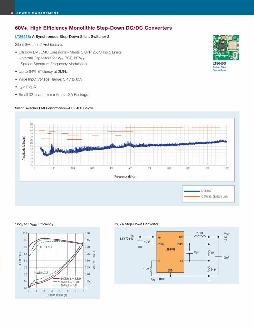
Silent Switcher EMI Performance—LT8650S Below
Ampl
itude
(dBu
Vim
)
LT8650S EMI/EMC Curve [email protected], [email protected], fsw = 2MHz with Spread Spectrum
LT8650S
CISPR 25, CLASS 5 Limit
LT8650S Actual Size Demo Board

5P O W E R M A N A G E M E N T
5V/4A, 3.3V/4A 2MHz Step-Down Converter
VIN2VIN23.7V TO 42V
VOUT23.3V4A
EN/UV2
LT8650S
SW2
FB2
VC2 VCC
SS2
4.7µF
1.5µH
BIAS
VIN1
EN/UV1
SW1
FB1
VC1VCC
SS1
RT
10nF
4.7pF 47µF1M
316k
VIN15.4V TO 42V
VOUT15V4A
4.7µF
10nF
47µF 4.7pF 1M
191k
2.2µH
1µF18.2k
fSW = 2MHz
GND SYNCVCC
Silent Switcher Synchronous Step-Down Regulators
Part Number Device Architecture
VIN Range (V) IOUT (A)
VOUT(MIN)(V) Frequency
Ext Sync Range IQ(µA) ISD(µA)
Max Junc Temp (˚C) Package
LT8608S* Silent Switcher 2 Synchronous Step-Down
3.0 to 42 1.5A 0.8 200kHz to 2.2MHz 200kHz to 3MHz 2.5 1 125 2x3 LGA-12
LT8609S* Silent Switcher 2 Synchronous Step-Down
3.0 to 42 2A/3A Peak 0.8 200kHz to 2.2MHz 200kHz to 3MHz 2.5 1 125 3x3 LGA-16
LT8641Silent Switcher Synchronous Step-Down
3.0 to 65 3.5 0.8 200kHz to 3MHz 200kHz to 3MHz 2.5 1 150 3x4 QFN-18
LT8614Silent Switcher Synchronous Step-Down
3.4 to 42 4 0.97 200kHz to 2.2MHz 200kHz to 2.2MHz 2.5 1 150 3x4 QFN-18
LT8640/-1Silent Switcher Synchronous Step-Down
3.4 to 42 5A/7A Peak 0.97 200kHz to 3MHz 200kHz to 3MHz 2.5 1 150 3x4 QFN-18
LT8640S* Silent Switcher 2 Synchronous Step-Down
3.4 to 42 5A/7A Peak 0.97 200kHz to 3MHz 200kHz to 3MHz 2.5 1 125 4x4 LGA-24
LT8643S* Silent Switcher 2 Synchronous Step-Down
3.4 to 42 5A/7A Peak 0.97 200kHz to 3MHz 200kHz to 3MHz 50 1 125 4x4 LGA-24
LT8653S* Dual Silent Switcher 2 Synchronous Step-Down
3.0 to 42 2A/3A Peak x 2 0.8 200kHz to 3MHz 200kHz to 3MHz 6 1 125 3x4 LGA-20
LT8650S* Dual Silent Switcher 2 Synchronous Step-Down
3.0 to 42 4A/6A Peak x 2 0.8 200kHz to 3MHz 200kHz to 3MHz 6.2 1 125 4x6 LGA-32
LT8645S* Silent Switcher 2 Synchronous Step-Down
3.4 to 65 7 0.8 200kHz to3MHz 200kHz to 3MHz 2.5 1 125 4x6 LGA-32
LT8642S* Silent Switcher 2 Synchronous Step-Down
3.4 to 18 10 0.6 200kHz to3MHz 200kHz to 3MHz 155 1 125 4x4 LGA-24
LT8652S* Dual Silent Switcher 2 Synchronous Step-Down
3.0 to 18 8.5A/12A Peak x 2 0.8 200kHz to3MHz 200kHz to 3MHz 6.2 1 125 4x7 LGA-36
*Silent Switcher 2: Internal Capacitors for VIN, BST, INTVCC
Silent Switcher µModule Regulator
Part Number Device Architecture
VIN Range (V) IOUT (A)
VOUT(MIN)(V) Frequency
Ext Sync Range IQ(µA) ISD(µA)
Max Junc Temp (˚C) Package
LTM8003Silent Switcher µModule Regulator
3.4 to 40 3.5A/6A Peak 0.97 200kHz to 3MHz 200kHz to 3MHz 25 3 150 6.25x9 BGA
P O W E R M A N A G E M E N T6
12VIN to 5VOUT Efficiency
Silent Switcher EMI Performance—LT8645S Below
5V, 7A Step-Down Converter
60V+, High Efficiency Monolithic Step-Down DC/DC Converters
Silent Switcher 2 Architecture:
• Ultralow EMI/EMC Emissions—Meets CISPR 25, Class 5 Limits
–Internal Capacitors for VIN, BST, INTVCC
–Spread Spectrum Frequency Modulation
• Up to 94% Efficiency at 2MHz
• Wide Input Voltage Range: 3 .4V to 65V
• IQ < 2 .5µA
• Small 32-Lead 4mm × 6mm LGA Package
LT8645S: A Synchronous Step-Down Silent Switcher 2
LT8645S
SW
BIAS
FB
V IN5.5V TO 65V
GND
RT
V IN
EN/UV
VOUT5V7A
100µF
10pF
4.7µF
41.2k
1M
243k
2.2µH
fSW = 1MHz
EFFICIENCY
POWER LOSS
500kHz, L = 3.3µH1MHz, L = 2.2µH2MHz, L = 1µH
LOAD CURRENT (A)
0 1 2 3 4 5 6 760
65
70
75
80
85
90
95
100
0
0.45
0.90
1.35
1.80
2.25
2.70
3.15
3.60
EFFI
CIEN
CY (%
)
POWER LOSS (W
)
LT8645S Actual Size Demo Board
0-15-10-505
101520253035404550
100 200 300 400 500 600 700 800 900 1000
Ampl
itude
(dBu
Vim
)
Frequency (MHz)
LT8645S
CISPR 25, CLASS 5 Limit
7P O W E R M A N A G E M E N T
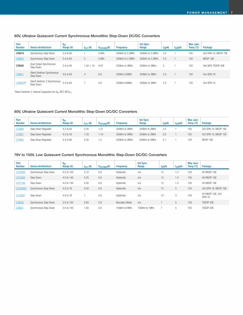
60V, Ultralow Quiescent Current Synchronous Monolithic Step-Down DC/DC Converters
Part Number Device Architecture
VIN Range (V) IOUT (A) VOUT(MIN)(V) Frequency
Ext Sync Range IQ(µA) ISD(µA)
Max Junc Temp (˚C) Package
LT8619 Synchronous Step-Down 3.4 to 65 1 0.985 200kHz to 2.2MHz 200kHz to 2.2MHz 2.5 1 150 3x3 DFN-10, MSOP-10E
LT8620 Synchronous Step-Down 3.4 to 65 2 0.985 200kHz to 2.2MHz 200kHz to 2.2MHz 2.5 1 150 MSOP-16E
LT8626 Dual Output Synchronous Step-Down
3.4 to 65 1.5A + 1A 0.97 200kHz to 3MHz 200kHz to 3MHz 5 1 150 3x6 QFN, TSSOP-28E
LT8641Silent Switcher Synchronous Step-Down
3.0 to 65 4 0.8 200kHz to3MHz 200kHz to 3MHz 2.5 1 150 3x4 QFN-18
LT8645S* Silent Switcher 2 Synchronous Step-Down
3.4 to 65 7 0.8 200kHz to3MHz 200kHz to 3MHz 2.5 1 150 3x4 QFN-18
*Silent Switcher 2: Internal Capacitors for VIN, BST, INTVCC
60V, Ultralow Quiescent Current Monolithic Step-Down DC/DC Converters
Part Number Device Architecture
VIN Range (V) IOUT (A) VOUT(MIN)(V) Frequency
Ext Sync Range IQ(µA) ISD(µA)
Max Junc Temp (˚C) Package
LT3990 Step-Down Regulator 4.2 to 62 0.35 1.21 200kHz to 2MHz 250kHz to 2MHz 2.5 1 150 3x3 DFN-10, MSOP-16E
LT3991 Step-Down Regulator 4.3 to 55 1.20 1.19 200kHz to 2MHz 250kHz to 2MHz 2.8 1 125 3x3 DFN-10, MSOP-10E
LT3995 Step-Down Regulator 4.3 to 60 2.50 1.2 200kHz to 2MHz 200kHz to 2MHz 2.7 1 150 MSOP-16E
76V to 150V, Low Quiescent Current Synchronous Monolithic Step-Down DC/DC Converters
Part Number Device Architecture
VIN Range (V) IOUT (A) VOUT(MIN)(V) Frequency
Ext Sync Range IQ(µA) ISD(µA)
Max Junc Temp (˚C) Package
LTC3639 Synchronous Step-Down 4.0 to 150 0.10 0.8 Hysteretic n/a 12 1.4 150 HV MSOP-16E
LTC3638 Step-Down 4.0 to 140 0.25 0.8 Hysteretic n/a 12 1.4 150 HV MSOP-16E
LTC7138 Step-Down 4.0 to 140 0.40 0.8 Hysteretic n/a 12 1.4 150 HV MSOP-16E
LTC3630A Synchronous Step-Down 4.0 to 76 0.50 0.8 Hysteretic n/a 12 5 150 3x5 DFN-16, MSOP-16E
LTC3637 Step-Down 4.0 to 76 1 0.8 Hysteretic n/a 12 3 150HV MSOP-16E, 3x5 DFN-16
LT8630 Synchronous Step-Down 3.0 to 100 0.60 0.8 Boundary Mode n/a 7 5 150 TSSOP-20E
LT8631 Synchronous Step-Down 3.0 to 100 1.00 0.8 100kHz to1MHz 100kHz to 1MHz 7 5 150 TSSOP-20E

P O W E R M A N A G E M E N T8
40V, Ultralow Quiescent Current Monolithic Switching Regulators
12VIN to 5VOUT Efficiency5V, 2MHz Step-Down
SYNC = 0VL = 3.3µHfSW = 2MHz
IOUT (mA)0 125 250 375 500 625 750
50
55
60
65
70
75
80
85
90
95
100
EFFI
CIEN
CY (%
)
VIN BST
EN/UVON OFF 0.1µF
22µF
10pF
4.7µF
VIN5.5V TO 42V
1µF
VOUT5V750mA
187k
3.3µHSYNC
INTVCC
TR/SS
RT
LT8607
GND
SW
PG
FB
18.2k
1M
L = XFL4020-332ME
• Wide Input Voltage Range: 3 .0V to 42V
• IQ < 2 .5µA
• 93% Efficiency at 2MHz
• Spread Spectrum Frequency Modulation for Low EMI
• 200kHz to 2 .2MHz Switching Frequency
• Small 10-Lead MSOP Package or 8-Lead 2mm × 2mm DFN Package
LT8607: 42V, 750mA, Synchronous Step-Down with Ultralow IQ
LT8607 Actual Size Demo Board

9P O W E R M A N A G E M E N T
42V, Ultralow Quiescent Current Synchronous Monolithic Switching Regulators
Part Number Device Architecture
VIN Range (V) IOUT (A)
VOUT(MIN)(V) Frequency Ext Sync Range IQ(µA) ISD(µA)
Max Junc Temp (˚C) Package
LT8606 Synchronous Step-Down 3.0 to 42 0.35 0.8 200kHz to 2.2MHz 200kHz to 3MHz 2.5 1 150 2x2 DFN-8, MSOP-10E
LT8607 Synchronous Step-Down 3.0 to 42 0.75 0.8 200kHz to 2.2MHz 200kHz to 3MHz 2.5 1 150 2x2 DFN-8, MSOP-10E
LT8608 Synchronous Step-Down 3.0 to 42 1.5 0.8 200kHz to 2.2MHz 200kHz to 3MHz 2.5 1 150 2x2 DFN-8, MSOP-10E
LT8608S* Silent Switcher 2Synchronous Step-Down
3.0 to 42 1.5 0.8 200kHz to 2.2MHz 200kHz to 3MHz 2.5 1 150 2x3 LGA-12
LT8609/A/B Synchronous Step-Down 3.0 to 42 2A/3A Peak 0.8 200kHz to 2.2MHz 200kHz to 3MHz 2.5 1 150 MSOP-10E
LT8609S* Silent Switcher 2 Synchronous Step-Down
3.0 to 42 2A/3A Peak 0.8 200kHz to 2.2MHz 200kHz to 3MHz 2.5 1 150 3x3 LGA-16
LT8610 Synchronous Step-Down 3.4 to 42 2.5 0.985 200kHz to 2.2MHz 200kHz to 2.2MHz 2.5 1 150 MSOP-16E
LT8610A Synchronous Step-Down 3.4 to 42 3.5 0.985 200kHz to 2.2MHz 200kHz to 2.2MHz 2.5 1 150 MSOP-16E
LT8610AB Synchronous Step-Down 3.4 to 42 3.5 0.985 200kHz to 2.2MHz 200kHz to 2.2MHz 2.5 1 150 MSOP-16E
LT8610AC Synchronous Step-Down 3.0 to 42 3.5 0.8 200kHz to 2.2MHz 200kHz to 2.2MHz 2.5 1 150 MSOP-16E
LT8610AX Synchronous Step-Down 3.4 to 42 3.5 0.985 200kHz to 2.2MHz 200kHz to 2.2MHz 2.5 1 175 MSOP-16E
LT8611Synchronous Step-Down with Current Sense
3.4 to 42 2.5 0.985 200kHz to 2.2MHz 200kHz to 2.2MHz 2.5 1 150 3x5 QFN-24
LT8697Synchronous Step-Down with Cable Comp
3.4 to 42 2.5 5V 300kHz to 2.2MHz 300kHz to 2.2MHz 3.6 1 150 3x5 QFN-24
LT3690 Synchronous Step-Down 3.9 to 36, 60MAX 4 0.8 170kHz to 1.5MHz 170kHz to 1.5MHz 70 1 150 4x6 QFN-26
LT8616Dual Output Synchronous Step-Down
3.4 to 42 2.5A + 1.5A 0.97 200kHz to 3MHz 200kHz to 3MHz 5 1 150 3x6 QFN-28, TSSOP-28E
LT8614Synchronous Silent Switcher Step-Down
3.4 to 42 4 0.97 200kHz to 2.2MHz 200kHz to 2.2MHz 2.5 1 150 3x4 QFN-18
LT8612 Synchronous Step-Down 3.4 to 42 5 0.985 200kHz to 2.2MHz 200kHz to 2.2MHz 2.5 1 150 3x6 QFN-28
LT8613Synchronous Step-Down with Current Sense
3.4 to 42 5 0.985 200kHz to 2.2MHz 200kHz to 2.2MHz 2.5 1 150 3x6 QFN-28
LT8640/-1 Silent Switcher Step-Down 3.4 to 42 5A/7A Peak 0.97 200kHz to 3MHz 200kHz to 3MHz 2.5 1 150 3x4 QFN-18
LT8640S* Silent Switcher 2 Synchronous Step-Down
3.4 to 42 5A/7A Peak 0.97 200kHz to 3MHz 200kHz to 3MHz 2.5 1 125 4x4 LGA-24
LT8643S* Silent Switcher 2 Synchronous Step-Down
3.4 to 42 5A/7A Peak 0.97 200kHz to 3MHz 200kHz to 3MHz 50? 1 125 4x4 LGA-24
LT8601Triple Output Synchronous Step-Down
3.0 to 422.5A + 1.5A + 1.8A
0.8 250kHz to 2.2MHz 250kHz to 2.2MHz 30 1 150 6x6 QFN-40
LT8602Quad Output Synchronous Step-Down
3.0 to 422.5A + 1.5A + 1.8A + 1.8A
0.8 250kHz to 2.2MHz 250kHz to 2.2MHz 25 1 150 6x6 QFN-40
LT8603Triple Output Synchronous Step-Down with Boost Controller
3.0 to 422.5A + 1.5A + 1.8A+1.8A
0.8 250kHz to 2.2MHz 250kHz to 2.2MHz 30 1 150 6x6 QFN-40
LT8653S* Dual Silent Switcher 2 Synchronous Step-Down
3.0 to 42 2A/3A Peak x 2 0.8 200kHz to 3MHz 200kHz to 3MHz 6 1 125 3x4 LGA-20
LT8650S* Dual Silent Switcher 2 Synchronous Step-Down
3.0 to 42 4A/6A Peak x 2 0.8 200kHz to 3MHz 200kHz to 3MHz 6.2 1 125 4x6 LGA-32
*Silent Switcher 2: Internal Capacitors for VIN, BST, INTVCC
40V, Ultralow Quiescent Current Monolithic Switching Regulators
Part Number Device Architecture
VIN Range (V) IOUT (A)
VOUT(MIN)(V) Frequency Ext Sync Range IQ(µA) ISD(µA)
Max Junc Temp (˚C) Package
LT3970 Step-Down 4.2 to 42 0.35 1.25 200kHz to 2.2MHz 200kHz to 2.2MHz 2.5 1 150 2x3 DFN-10, MSOP-10
LT3973 Step-Down 4.3 to 42 0.75 1.21 200kHz to 2.2MHz 250kHz to 2.2MHz 2.5 1 150 3x3 DFN-10, MSOP-10E
LT3971 Step-Down 4.3 to 38 1.2 1.19 200kHz to 2.2MHz 200kHz to 2.2MHz 2.8 1 125 3x3 DFN-10, MSOP-10E/16E
LT3975 Step-Down 4.3 to 42 2.50 1.2 200kHz to 2MHz 200kHz to 2MHz 2.7 1 150 MSOP-16E
LT3976 Step-Down 4.3 to 40 5.00 1.2 200kHz to 2MHz 200kHz to 2MHz 3.3 1 150 MSOP-16E

P O W E R M A N A G E M E N T1 0
60VIN to 150VIN Max Input DC/DC Controllers
• Wide VIN Range: 4V to 140V (150V Abs Max)
• Wide Output Voltage Range: 0 .8V to 60V
• Adjustable Gate Drive Level: 5V to 10V
• Low Operating IQ: 40μA (Shutdown = 10μA)
• 100% Duty Cycle Operation
• No External Bootstrap Diode Required
LTC3895: 150V Low IQ, Synchronous Step-Down DC/DC Controller
0.1µF
4.7µF 6mΩ
511k
150µF
36.5k
1nF
0.1µF
0.1µF
10k
4.7nF
100pF
100µF
33µH
30.1k
V IN
INTV CC
CPUMP_EN
ITH
SS
FREQ
GND
LTC3895
TG
SW
BG
SENSE+
SENSE–
EXTV CC
VFB
BOOST
RUNNDRV
DRV CC
V IN7V to 140V
VOUT12V*5A
x3
*VOUT FOLLOWS VIN WHEN VIN < 12V
60VIN to 150VIN Max Input, Low Quiescent Current DC/DC Controllers
Part Number Device Architecture
VIN Range (V) IOUT (A) VOUT(MIN)(V)
Frequency (kHz)
Ext Sync Range (kHz) IQ(µA) ISD(µA)
Max Junc Temp (˚C) Package
LTC3895 Synchronous Step-Down 4 to 150 20 0.8 50 to 900 75 to 850 40 10 150 TSSOP-38 (31)
LTC3892 Synchronous Step-Down 4 to 60 2 X 20 0.8 50 to 900 75 to 850 28 14 150 QFN-32/TSSOP-28
LTC3891 Synchronous Step-Down 4 to 60 20 0.8 50 to 900 75 to 750 50 14 150 QFN-20, TSSOP-20E
LT3840 Synchronous Step-Down 2.5 to 60 20 1.23 50 to 1MHz 50 to 1MHz 75 10 150 QFN-38/TSSOP-28
LT3845A Synchronous Step-Down 4 to 60 20 1.23 100 to 600 100 to 600 120 10 125 TSSOP-16E
LTC7813 Synchronous Buck + Boost 4.5 to 60 2 X 10 0.8 75 to 850 75 to 850 29 10 150 QFN-32
LTC3864 Step-Down 3.5 to 60 5 0.8 50 to 850 75 to 750 40 7 150 DFN-12
LTC3863 Inverter 3.5 to 60 5 -0.4 50 to 850 75 to 750 70 7 150 DFN-12, MSOP-12
LTC3897Synchronous Step-Up with Protection
4.5 to 75 20 Up to 60 50 to 900 75 to 850 55 15 150 QFN-38, TSSOP-38
LTC3784 Synchronous Step-Up 4.5 to 60 20 Up to 60 50 to 900 75 to 850 28 8 150 QFN-28, SSOP-28
LTC3769 Synchronous Step-Up 4.5 to 60 10 Up to 60 50 to 900 75 to 850 28 4 150 QFN-24, SSOP-20
LTC3859AL Buck/Buck/Boost 4.3 to 60 10/10/10 0.8 50 to 900 75 to 850 29 3.6 150 QFN-38, TSSOP-38
80VIN to 100VIN Max Input DC/DC Controllers
Part Number Device Architecture
VIN Range (V) IOUT (A) VOUT(MIN)(V)
Frequency (kHz)
Ext Sync Range (kHz) IQ(µA) ISD(µA)
Max Junc Temp (˚C) Package
LTC3871Bidirectional Synchronous Buck or Boost
Up to 100 20 1.2 60 to 460 60 to 460 8mA 140 150 LPFQ-48
LT3748 Flyback 5 to 100 5 1.22 Variable n/a 1.3mA 1 150 MSOP-16 (12)
LT3758ABoost, Flyback, SEPIC and Inverting
5.5 to 100 5 1.6/-0.8 100 to 1MHz 100 to 1MHz 1.75mA 0.1 150 DFN-10, MSOP-10
LTC3810 Synchronous Buck 6.2 to 100 20 6.2 100 to 1MHz 100 to 1MHz 3mA 240 125 TSSOP-16E
LT8710 Synchronous SEPIC 4.5 to 80 10 0 70 to 700 70 to 700 4mA 1 125 TSSOP-20
LTC3895 Actual Size Demo Board
LTC3895 Back side of Demo Board

1 1P O W E R M A N A G E M E N T
40V, Step-Down DC/DC Converters with Cable Drop Compensation for USB Applications
2MHz 5V Step-Down Converter with Cable Drop Compensation and Output Current Monitor
Transient Response with 0.24Ω Total RLINE
EN/UV
PG
INTVCC
ICTRL
SYNC
TR/SS
RT
SW
SYS
ISP
ISN
USB5V
RCBL
VIN
VIN6V TO 42V
BST3.3µH 0.018Ω
GND
LT8697
1µF
16.5k PGND
10nF
4.7µF
0.1µF
47µF×2
18.2k
0.1Ω
3 METERS AWG 20TWISTED PAIR CABLE
0.1Ω
10k
1nF
VOUT
LOAD VLOAD
5V, 2.4A
+
–
VOLT
AGE
(V) CURRENT (A)
5.00
5.25
5.50
4.75
4.50
4.25
3
4
5
2
1
0100µs/DIV
VOUT
VLOAD
ILOAD50mA/µs
• Accurate 5V Output: ±1 .4% Over Full Operating Junction
Temperature Range
• Programmable Cable Drop Compensation
• Programmable Output Current Limit
• Output Current Monitor
• Dual Input Feedback Permits Regulation on Output of USB Switch
• Forced Continuous Mode for Fast Load Step Low Recovery
• Ultralow Quiescent Current Burst Mode® Operation: 3 .6μA IQ
Regulation 12VIN to 5VOUT
LT8697: 42V, 2.5A Synchronous Buck Regulator with Cable Drop Compensation for USB Applications
40V, Low Quiescent Current Monolithic Regulators with Cable Compensation
Part Number Device Architecture
VIN Range (V) IOUT (A)
VOUT(MIN)(V) Frequency Ext Sync Range IQ(µA) ISD(µA)
Max Junc Temp (˚C) Package
LT3086 Low Dropout Linear Regulator 1.65 to 40 2.1 0.4 n/a n/a 1.2mA 1 1255x4 QFN-16, TSSOP-16E, DD-7, TO-220
LT8697Synchronous Step-Down with Cable Comp
3.4 to 42 2.5 5V 300kHz to 2.2MHz 300kHz to 2.2MHz 3.6 1 150 3x5 QFN-24
LT3697 Step-Down w/ Cable Comp 5 to 40, 60MAX 2.50 5.00 200kHz to 2.2MHz 200kHz to 2.2MHz 700 1 150 MSOP-16E
P O W E R M A N A G E M E N T1 2
LT8602 Actual Size Demo Board
EFFICIENCY
POWERLOSS
FSW = 1MHzFSW = 2MHz
LOAD CURRENT (A)0 0.3 0.6 0.9 1.2 1.5
0
10
20
30
40
50
60
70
80
90
100
0
0.2
0.4
0.6
0.8
1.0
1.2
1.4
1.6
1.8
2.0
EFFI
CIEN
CY (%
)
POWER LOSS (W
)
EFFICIENCY
POWERLOSS
FSW = 1MHzFSW = 2MHz
LOAD CURRENT (A)0 0.3 0.6 0.9 1.2 1.5 1.8
0
10
20
30
40
50
60
70
80
90
100
0
0.1
0.2
0.3
0.4
0.5
0.6
0.7
0.8
0.9
1.0
EFFI
CIEN
CY (%
)
POWER LOSS (W
)
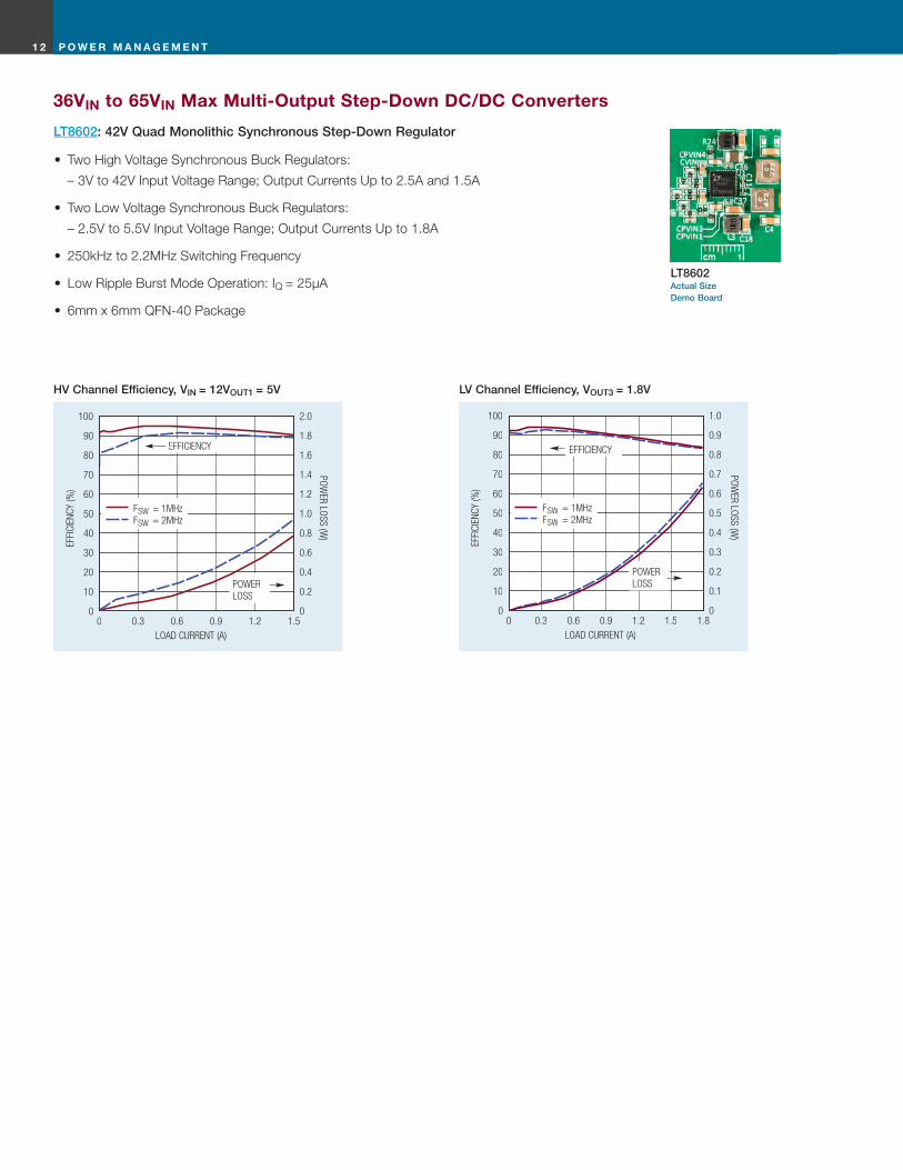
36VIN to 65VIN Max Multi-Output Step-Down DC/DC Converters
HV Channel Efficiency, VIN = 12VOUT1 = 5V LV Channel Efficiency, VOUT3 = 1.8V
• Two High Voltage Synchronous Buck Regulators:
– 3V to 42V Input Voltage Range; Output Currents Up to 2 .5A and 1 .5A
• Two Low Voltage Synchronous Buck Regulators:
– 2 .5V to 5 .5V Input Voltage Range; Output Currents Up to 1 .8A
• 250kHz to 2 .2MHz Switching Frequency
• Low Ripple Burst Mode Operation: IQ = 25μA
• 6mm x 6mm QFN-40 Package
LT8602: 42V Quad Monolithic Synchronous Step-Down Regulator
1 3P O W E R M A N A G E M E N T
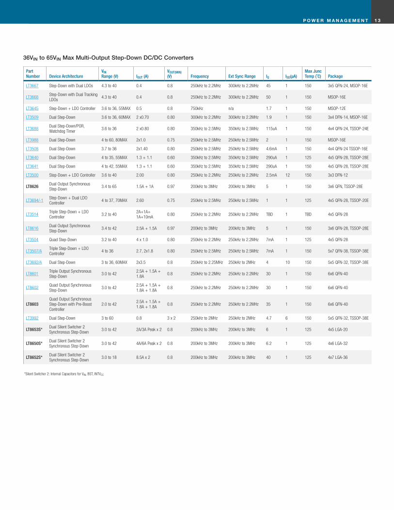
36VIN to 65VIN Max Multi-Output Step-Down DC/DC Converters
Part Number Device Architecture
VIN Range (V) IOUT (A)
VOUT(MIN)(V) Frequency Ext Sync Range IQ ISD(µA)
Max Junc Temp (˚C) Package
LT3667 Step-Down with Dual LDOs 4.3 to 40 0.4 0.8 250kHz to 2.2MHz 300kHz to 2.2MHz 45 1 150 3x5 QFN-24, MSOP-16E
LT3668Step-Down with Dual Tracking LDOs
4.3 to 40 0.4 0.8 250kHz to 2.2MHz 300kHz to 2.2MHz 50 1 150 MSOP-16E
LT3645 Step-Down + LDO Controller 3.6 to 36, 55MAX 0.5 0.8 750kHz n/a 1.7 1 150 MSOP-12E
LT3509 Dual Step-Down 3.6 to 36, 60MAX 2 x0.70 0.80 300kHz to 2.2MHz 300kHz to 2.2MHz 1.9 1 150 3x4 DFN-14, MSOP-16E
LT3688Dual Step-Down/POR, Watchdog Timer
3.6 to 36 2 x0.80 0.80 350kHz to 2.5MHz 350kHz to 2.5MHz 115uA 1 150 4x4 QFN-24, TSSOP-24E
LT3988 Dual Step-Down 4 to 60, 80MAX 2x1.0 0.75 250kHz to 2.5MHz 250kHz to 2.5MHz 2 1 150 MSOP-16E
LT3508 Dual Step-Down 3.7 to 36 2x1.40 0.80 250kHz to 2.5MHz 250kHz to 2.5MHz 4.6mA 1 150 4x4 QFN-24 TSSOP-16E
LT3640 Dual Step-Down 4 to 35, 55MAX 1.3 + 1.1 0.60 350kHz to 2.5MHz 350kHz to 2.5MHz 290uA 1 125 4x5 QFN-28, TSSOP-28E
LT3641 Dual Step-Down 4 to 42, 55MAX 1.3 + 1.1 0.60 350kHz to 2.5MHz 350kHz to 2.5MHz 290uA 1 150 4x5 QFN-28, TSSOP-28E
LT3500 Step-Down + LDO Controller 3.6 to 40 2.00 0.80 250kHz to 2.2MHz 250kHz to 2.2MHz 2.5mA 12 150 3x3 DFN-12
LT8626 Dual Output Synchronous Step-Down
3.4 to 65 1.5A + 1A 0.97 200kHz to 3MHz 200kHz to 3MHz 5 1 150 3x6 QFN, TSSOP-28E
LT3694/-1Step-Down + Dual LDO Controller
4 to 37, 70MAX 2.60 0.75 250kHz to 2.5MHz 250kHz to 2.5MHz 1 1 125 4x5 QFN-28, TSSOP-20E
LT3514Triple Step-Down + LDO Controller
3.2 to 402A+1A+ 1A+10mA
0.80 250kHz to 2.2MHz 250kHz to 2.2MHz TBD 1 TBD 4x5 QFN-28
LT8616Dual Output Synchronous Step-Down
3.4 to 42 2.5A + 1.5A 0.97 200kHz to 3MHz 200kHz to 3MHz 5 1 150 3x6 QFN-28, TSSOP-28E
LT3504 Quad Step-Down 3.2 to 40 4 x 1.0 0.80 250kHz to 2.2MHz 250kHz to 2.2MHz 7mA 1 125 4x5 QFN-28
LT3507/ATriple Step-Down + LDO Controller
4 to 36 2.7, 2x1.8 0.80 250kHz to 2.5MHz 250kHz to 2.5MHz 7mA 1 150 5x7 QFN-38, TSSOP-38E
LT3692/A Dual Step-Down 3 to 36, 60MAX 2x3.5 0.8 250kHz to 2.25MHz 250kHz to 2MHz 4 10 150 5x5 QFN-32, TSSOP-38E
LT8601Triple Output Synchronous Step-Down
3.0 to 422.5A + 1.5A + 1.8A
0.8 250kHz to 2.2MHz 250kHz to 2.2MHz 30 1 150 6x6 QFN-40
LT8602Quad Output Synchronous Step-Down
3.0 to 422.5A + 1.5A + 1.8A + 1.8A
0.8 250kHz to 2.2MHz 250kHz to 2.2MHz 30 1 150 6x6 QFN-40
LT8603Quad Output Synchronous Step-Down with Pre-Boost Controller
2.0 to 422.5A + 1.5A + 1.8A + 1.8A
0.8 250kHz to 2.2MHz 250kHz to 2.2MHz 35 1 150 6x6 QFN-40
LT3992 Dual Step-Down 3 to 60 0.8 3 x 2 250kHz to 2MHz 250kHz to 2MHz 4.7 6 150 5x5 QFN-32, TSSOP-38E
LT8653S* Dual Silent Switcher 2 Synchronous Step-Down
3.0 to 42 2A/3A Peak x 2 0.8 200kHz to 3MHz 200kHz to 3MHz 6 1 125 4x5 LGA-20
LT8650S* Dual Silent Switcher 2 Synchronous Step-Down
3.0 to 42 4A/6A Peak x 2 0.8 200kHz to 3MHz 200kHz to 3MHz 6.2 1 125 4x6 LGA-32
LT8652S* Dual Silent Switcher 2 Synchronous Step-Down
3.0 to 18 8.5A x 2 0.8 200kHz to 3MHz 200kHz to 3MHz 40 1 125 4x7 LGA-36
*Silent Switcher 2: Internal Capacitors for VIN, BST, INTVCC

P O W E R M A N A G E M E N T1 4
36VIN to 40VIN Max Input Low Quiescent Current Synchronous DC/DC Controllers
Efficiency and Power Loss vs Output Current
IOUT (A)
Burst Mode OPERATION
0
EFFI
CIEN
CY (%
)
POWER LOSS (W
)
70
100
10.10.010.0010.0001 10
50
40
30
200.01
0.1
1
10
0.001
10
60
80
90VIN = 24VVOUT = 12V
POWER LOSS
EFFICIENCY
• Wide VIN Range: 4V to 38V (40V Abs Max)
• Low Operating IQ: 50μA
• Wide Output Voltage Range: 0 .8V ≤ VOUT ≤ 24V
• RSENSE or DCR Current Sensing
• Phase-Lockable Frequency (75kHz to 750kHz)
• Programmable Fixed Frequency (50kHz to 900kHz)
• Selectable Continuous, Pulse-Skipping or Low Ripple Burst Mode
Operation at Light Load
LTC3807: Low IQ, Synchronous Step-Down Controller with 24V Output Voltage Capability
0.1µF
22µF12.5V TO VIN 38V
60.4k
15.4k4.7nF
100k
6.98k
2.2µF
47pF
0.1µF
FREQ
ITH
SGND
EXTVCCVOUT
LTC3807
VIN INTVCC
10µH 4mΩ
INTVCC
BOOST
SW
BG
PGND
SENSE–
SENSE+
TG
100k
150µF
VOUT12V10A
TRACK/SS
VFB
PGOOD
36VIN to 38VIN Max Input Low Quiescent Current Synchronous DC/DC Controllers
Part Number Device Architecture
VIN Range (V) IOUT (A)
VOUT(MIN)(V)
Frequency (kHz)
Ext Sync Range (kHz) IQ(µA) ISD(µA)
Max Junc Temp (˚C) Package
LTC3807 Synchronous Step-Down 4 to 38 25 0.8 50 to 900 75 to 850 50 14 150 QFN-20, TSSOP-20
LTC7812 Synchronous Buck + Boost 4.5 to 38 2 X 10 0.8 75 to 850 75 to 850 28 10 150 QFN-32
LTC3834 Synchronous Step-Down 4 to 36 25 0.8 140 to 650 140 to 650 30 14 125 DFN-16, SSOP-16
LTC3834-1 Synchronous Step-Down 4 to 36 25 0.8 140 to 650 140 to 650 30 14 125 QFN-20, TSSOP-20
LTC3857/-1 Dual Synchronous Step-Down 4 to 38 20/20 0.8 140 to 650 50 to 900 50 8 125 QFN-32/SSOP-28
LTC3859AL Buck/Buck/Boost 4.5 to 38 10/10/10 0.8 50 to 900 75 to 850 28 10 150 QFN-38/TSSOP-38
LTC3786 Synchronous Step-Up 4.5 to 38 10 Up to 60 50 to 900 75 to 850 50 14 150 QFN-20, TSSOP-20
LTC3787 Synchronous Step-Up 4.5 to 38 20 Up to 60 50 to 900 75 to 850 135 8 150 QFN-28, SSOP-28
LTC3788/-1 Synchronous Step-Up 4.5 to 38 10/10 Up to 60 50 to 900 75 to 850 125 8 150 QFN-32
36VIN to 40VIN Max Input DC/DC Controllers
Part Number Device Architecture
VIN Range (V) IOUT (A)
VOUT(MIN)(V)
Frequency (kHz)
Ext Sync Range (kHz) IQ(µA) ISD(µA)
Max Junc Temp (˚C) Package
LTC3851A/-1 Synchronous Step-Down 4 to 40 25 0.8 250 to 750 250 to 750 1mA 15 150 QFN-16, SSOP-16
LTC3878 Synchronous Step-Down 4 to 38 25 0.8 Constant On-Time n/a 1.5mA 18 125 SSOP-16
LTC3879 Synchronous Step-Down 4 to 38 25 0.6 Constant On-Time n/a 1.5mA 18 125 QFN-16, MSOP-16
LTC3854 Synchronous Step-Down 4.5 to 38 25 0.8 400 n/a 2mA 15 125 MSOP-12, DFN-12
LTC3866 Synchronous Step-Down 4.5 to 36 25 0.6 250 to 770 250 to 770 3.2mA 30 125 QFN-24, TSSOP-24
LTC3839 2-Phase Synchronous Step-Down 4.5 to 38 50 0.6 200 to 2MHz 200 to 2MHz 3mA 15 125 QFN-32
LTC3855 Dual Synchronous Step-Down 4.5 to 38 25/25 0.6 250 to 770 250 to 770 3.5mA 30 125 QFN-40, SSOP-38
LTC3869/-2 Dual Synchronous Step-Down 4 to 38 25/25 0.6 250 to 780 250 to 780 3mA 30 125 QFN-28, TSSOP-28
LTC3862/-1/-2 2-Phase Step-Up 4 to 36 8 * 50 to 650 50 to 650 1.8mA 30 150QFN-24, SSOP-24, TSSOP-24
LT3757A Boost, Flyback, SEPIC and Inverting 2.9 to 40 4 3.3 100 to 1MHz 100 to 1MHz 1.6mA 1 150 DFN-10, MSOP-10
* Dependent on External Components
LTC3807 50% Scale Demo Board

1 5P O W E R M A N A G E M E N T
High Voltage Power Managers and Battery Chargers
Efficiency and Power Loss vs Output Current
• Wide Voltage Range: 4 .5V to 55V Input, Up to 55V Output (60V
Absolute Maximums)
• Synchronous Buck-Boost DC/DC Controller
• Li-Ion and Lead-Acid Charge Algorithms
• ±0 .5% Float Voltage Accuracy
• ±5% Charge Current Accuracy
• Instant-On for Heavily Discharged Batteries
• Ideal Diode Controller Provides Low Loss PowerPath
• When Input Power is Limited
• Input Voltage Regulation for High Impedance Input Supplies and
Solar Panel Peak Power Operation
• Onboard Timer for Protection and Termination
• Bad Battery Detection with Auto-Reset
• NTC Input for Temperature Qualified Charging
• Binary Coded Open-Collector Status Pins
• Low Profile (0 .75mm) 38-Pin 5mm × 7mm QFN Package
LTC4020: 55V Buck-Boost Multi-Chemistry Battery Charger
LTC4020
RNTC
RSENSEB
RSENSEABUCK-BOOST
DC/DC CONVERTER PowerPath BATTERY CHARGERVIN VOUT
RCS
BG1
TG1
SENSBOT
SENSTOP
SENSVIN
BG2
TG2
VFBMAX
CSP
CSN
BGATE
VFB
NTC
SENSGND
High Voltage Battery Chargers and Power Managers
Part Number
Charge Current Wall (A)
# of Battery Cells (Series)
Max Charge Current USB (mA)
Power Manager Topology Input Voltage (V)
Standby Current (µA) Other Features
Charge Termination
PowerPath™ Control Package
LTC4079 0.25Up to 60V Lead- Acid Li-ion LiFePO4
0.25 n/a 1.2V to 60V 4 MPPC (DVReg) Timer + C/10 n/a 3x3 DFN-10
LTC4121 0.4 3.6V to 18V n/a Switching 4.3V to 40V 2.5 <1 Timer n/a 3x3 QFN-16
LTC4089* 1.2 1 500 Linear4.35V to 5.5V USB, 6 to 36V, 40V Max Adapter
50 2.5 Timer + C/10 yes 3x6 DFN-22
LTC4089-5 1.2 1 500 Linear4.35V to 5.5V USB, 6V to 36V, 40V Max Adapter
50 2.5 Timer + C/10 yes 3x6 DFN-22
LTC4089-1*& 1.2 1 500 Linear4.35V to 5.5V USB, 6V to 36V, 40V Max Adapter
50 2.5 Timer + C/10 yes 3x6 DFN-22
LTC4090 1.2 1 500 Linear4.35V to 5.5V USB, 6V to 38V, 60V Max Adapter
50 2.5 Timer + C/10 yes 3x6 DFN-22
LTC4098* 1.5 1 700Buck Switching
4.35V to 5.5V USB, 6V to 38V & 60V Transient Adapter, 66V OVP
25 3.5 Timer + C/10 yes 3x4 QFN-20
LT3650-4.2/8.4 2 1-2 n/aBuck Switching
4.75V to 32V / 9V to 32V, 40V Abs Max
85 15 Timer + C/10 n/a 3x3 DFN-12, TSSOP-16
LT3652/HV 2 3.3V-14.4/18V n/aBuck Switching
4.95V to 32/34V, 40V Abs Max
85 15 Timer + C/10 n/a 3x3 DFN-12, MSOP-12E
LTC4015 20A ^Up to 35V Lead- Acid Li-ion LiFePO4
n/aBuck Switching
4.5V to 35V 112MPPT, ADC, Coulomb Ctr, Dig Telemetry
Timer + C/x yes 5x7 QFN-38
LTC4013 20A ^Up to 60V Lead- Acid Li-ion LiFePO4
n/aBuck Switching
4.5V to 60V 480 MPPT Timer + C/10INFET only (no BATFET)
4x5 QFN-28
LTC4020 20A ^Up to 55V Lead- Acid Li-ion LiFePO4
n/aBuck-Boost Switching
4.5V to 55V 30 MPPC Timer + C/10 yes 5x7 QFN-38
LTC4000/-1** >20A 3V to 60V n/a n/a 3V to 60V 400 MPPC (-1) Timer or C/x external 4x5 QFN-28, SSOP-28
* Bat-Track adaptive output control & 4.1V cell voltage ^ depends on external components ** Battery charging controller – works in conjunction with externally compensated switching regulator
For a more detailed review of Linear’s extensive portfolio of battery chargers, see the Battery Charging and Management Solutions Brochure.

P O W E R M A N A G E M E N T1 6
LTC3256 Actual Size Demo Board
High Voltage Charge Pumps
High Efficiency Dual Output Power Supply
Power Dissipation vs Input Voltage
6 7 8 9 10 11 12 13 14 15 16
INPUT VOLTAGE (V)
0.0
0.5
1.0
1.5
2.0
2.5
3.0
3.5
4.0
4.5
5.0PO
WER
DIS
SIPA
TION
(W)
3.3V LOAD = 250mA5V LOAD = 100mA
LTC3256
IDEAL DUAL LDO
• Input Voltage Range: 5 .5V to 38V
• Independently Enabled 5V and 3 .3V Fixed Outputs
• 5V Output: 100mA Max
• 3 .3V LDO Output: 250mA Max
• Multimode Step-Down Charge Pump (2:1, 1:1) with
Automatic Mode Switching
• Low Quiescent Current: 20μA with Both Outputs Regulating
(No Load)
• Engineered for Diagnostic Coverage in ISO 26262 Systems
• 1 .1V Reference Output for System Diagnostics
• Power-On Reset and Watchdog Controller with
Adjustable Timing
• Overcurrent Fault Protection on Each Output
• Overtemperature Protection
• 150°C Max Operating Junction Temperature
• Thermally Enhanced 16-Lead MSOP Package
LTC3256: Wide VIN Range Dual Output 350mA Step-Down Charge Pump with Watchdog Timer
10µF
10µF
10µF
10µF1M
MICROCONTROLLERINTERFACE
5V OUTPUT100mA MAX
3.3V LDO OUTPUT250mA MAX
5.5V TO 38VINPUT SUPPLY
OUTCP
OUT5
OUT3
PG3PG5
RSTI
REFOUT
RSTWDI
VIN
EN5EN3
RTWT
GND
LTC3256
1µF
C+ C–
0.1µF
High Voltage Charge Pumps
Part Number VIN Range (V) VOUT (V) IQ Max IOUT Topology LDO Post Regulator Max Junc Temp (˚C) Package
LTC3255 4 – 48 2.4 to 12.5 20µA 50mA Step-Down No 150 3x3 DFN-10, MSOP-10E
LTC3260 4.5 – 32 ±Adj 100µA 100mA Dual/Inverting Yes 150 3x4 DFN-14, MSOP-16E
LTC3265 4.5 – 32 ±1.2V to ±VIN 135µA 100mA Boost/Inv + 2 LDOs Yes 150 3x5 DFN-18, TSSOP-20E
LTC3261 4.5 – 32 -VIN 60µA 100mA Inverting No 150 MSOP-12E
LTC3245 2.7 – 38 3.3, 5, Adj 18µA 250mA Buck-Boost No 150 3x4 DFN-12, MSOP-12E
LTC3256 5.5 – 38 5 / 3.3 18µA 100/250mA Step-Down + LDO Yes 150 MSOP-16E

1 7P O W E R M A N A G E M E N T
LTC3265 Actual Size Demo Board
Low Noise ±15V Outputs from a Single 12V Input
LDO Rejection of VOUT ±Ripple
VIN_N
CBST+ CBST–
LTC3265
RT
1µF
VOUT+
VIN_P
10µF
10µF
10µF
+15V12V
–15V
604K
52.3k
52.3k
604K
100nF
100nF
10µF
1µF
10µF
LDO+
EN+ ADJ+
EN– BYP+
MODE GND
CINV+ BYP–
CINV– ADJ–
VOUT– LDO–
VOUT+
10mV/DIVAC-COUPLED
VLDO+
10mV/DIVAC-COUPLED
VLDO–
10mV/DIVAC-COUPLED
VOUT–
10mV/DIVAC-COUPLED
1µs/DIV
VIN_P = 12V, VIN_N = VOUT+
VLDO+ = 15V
VLDO– = –15V
fOSC = 500kHz
ILDO+ = 20mA
ILDO– = –20mA
• Boost Charge Pump Generates 2 • VIN_P (VIN_P Range:
4 .5V to 16V)
• Inverting Charge Pump Generates –VIN_N (VIN_N Range:
4 .5V to 32V)
• Low Noise Positive LDO Post Regulator Up to 50mA
• Low Noise Negative LDO Post Regulator Up to 50mA
• 135μA Quiescent Current in Burst Mode Operation with Both
LDO Regulators On
• 50kHz to 500kHz Programmable Oscillator Frequency
• Stable with Ceramic Capacitors
• Short-Circuit/Thermal Protection
• Low Profile 3mm × 5mm 18-Lead DFN and Thermally Enhanced
20-Lead TSSOP Packages
LTC3265: Low Noise Dual Supply with Boost and Inverting Charge Pumps

P O W E R M A N A G E M E N T1 8
Low Voltage (<6VIN) Point-of-Load Synchronous Step-Down Switching Regulators
• 8-Channel 1A Independent Step-Down DC/DCs
• Master-Slave Configurable for Up to 4A of Output Current with a Single Inductor
• Independent 2 .25V to 5 .5V VIN Supplies for Each DC/DC
• All DC/DCs Have 0 .8V to VIN Output Range
• ±1% VFB Accuracy, for Buck 1 (1A to 4A)
• Thermally Enhanced 38-Lead 5mm × 7mm QFN and TSSOP Packages
LTC3374A: High Accuracy 8-Channel Parallelable 1A Buck DC/DC Converter
Eight Synchronous 1A Buck Regulators Buck Efficiency vs ILOAD
VOUT = 1.8V
1A BUCK, L = 4.7µH, L DCR = 40mΩ2A BUCK, L = 2.2µH, L DCR = 13mΩ3A BUCK, L = 1.8µH, L DCR = 10mΩ4A BUCK, L = 1.0µH, L DCR = 8mΩ
LOAD CURRENT (A)1m 10m 100m 1 4
0
10
20
30
40
50
60
70
80
90
100
EFFI
CIEN
CY (%
)
fOSC = 1MHzVIN = 3.3V
VOUT = 1.8VBurst Mode OPERATION
BUCK 10.8V TO VIN1UP TO 1A
SW1
2.7V TO 5.5V
2.25V TO 5.5V
2.25V TO 5.5V SW2VIN2
SW8VIN8
FB1
FB2
FB8
VIN1
BUCK 20.8V TO VIN2UP TO 1A
EN2
EN8
2.25V TO 5.5V
EN1
BUCK 80.8V TO VIN8UP TO 1A
GND
LTC3374A •••
•••
PGOOD_ALLTEMP
VCCMODESYNC
RT
THE EIGHT BUCKS CAN BE CONFIGURED IN 15 DIFFERENT MASTER/SLAVE COMBINATIONS
LTC3374 Actual Size Demo Board

1 9P O W E R M A N A G E M E N T
Low Voltage (<6VIN) Point-of-Load Synchronous Step-Down Switching Regulators
Part Number Device Architecture
VIN Range (V) IOUT (A)
VOUT(MIN)(V)
Frequency (MHz)
Ext Sync Range (MHz) IQ(µA) ISD(µA)
Max Junc Temp (˚C) Package
LTC3410/B Synchronous 2.5 to 5.5 0.3 0.8 2.25 n/a 26 1 125 SC70
LTC3542 Synchronous 2.5 to 5.5 0.5 0.6 2.25 1 to 3 26 1 125 2x2 DFN-6, ThinSOT™
LTC3547/B Dual Synch 2.5 to 5.5 0.3/0.3 0.6 2.25 n/a 40 1 125 2x3 DFN-8
LTC3406A/AB Synchronous 2.5 to 5.5 0.6 0.6 1.5 n/a 20 1 125 ThinSOT
LTC3406AB-2 Synchronous 2.5 to 5.5 0.6 0.6 2.25 1.4 to 4 200 1 125 ThinSOT
LTC3448 Synchronous 2.5 to 5.5 0.6 0.6 2.25 1 to 3 32 1 125 MSOP-8E, DFN-8
LTC3543 Synchronous 2.5 to 5.5 0.6 0.6 2.25 1 to 3 45 1 125 2x3 DFN-6
LTC3544/B Quad Synch 2.25 to 5.5 0.3/0.2/0.2/0.1 0.8 2.25 n/a 80 1 125 3x3 QFN-16
LTC3560 Synchronous 2.5 to 5.5 0.8 0.6 2.25 1 to 3 16 1 125 ThinSOT
LTC3561 Synchronous 2.6 to 5.5 1 0.8 850kHz to 4MHz n/a 240 1 125 3x3 DFN-10
LTC3446 Synchronous + LDOs 2.7 to 5.5 1.0/0.3/0.3 0.4 2.25 n/a 140 1 125 4x3 DFN-14
LTC3407A Dual Synch 2.5 to 5.5 0.6/0.6 0.6 1.5 1.5MHz 40 1 125 MSOP-10, 3x3 DFN-10
LTC3409 Dual Synch 1.6 to 5.5 0.6/0.6 0.6 1.7/2.6 1MHz to 3MHz 65 1 125 3x3 DFN-8
LTC3419 Dual Synch 2.5 to 5.5 0.6/0.6 0.6 2.25 n/a 55 1 125 MSOP-10, 3x3 DFN-10
LTC3548 Dual Synch 2.5 to 5.5 0.8/ 0.4 0.6 2.25 2.25 40 1 125 MSOP-10, 3x3 DFN-10
LTC3411A Synchronous 2.5 to 5.5 1.25 0.8 300kHz to 4.0MHz 400kHz to 4MHz 40 1 125 3x3 DFN-10, MSOP-10
LTC3407A-2 Synchronous 2.5 to 5.5 0.8/ 0.8 0.6 2.25 2.25 40 1 125 MSOP-10, 3x3 DFN-10
LTC3568 Synchronous 2.5 to 5.5 1.8 0.8 850kHz to 4MHz 400kHz to 4MHz 60 1 125 3x3 DFN-10,
LTC3417A-2 Dual Synch 2.25 to 5.5 1.5/1.0 0.8 2.25 2.25 125 1 125 TSSOP-20E, 3x5 DFN-20
LTC3545 Triple Synch 2.25 to 5.5 0.8/0.8/0.8 0.6 2.25 1 to 3 58 1 125 3x3 QFN-16
LTC3612 Synchronous 2.25 to 5.5 3.0 0.6 300kHz to 4.0MHz 300kHz to 4.0MHz 70 1 150 TSSOP-20E, 3x4 QFN-20
LTC3412A Synchronous 2.25 to 5.5 3.0 0.8 300kHz to 4.0MHz 300kHz to 4.0MHz 64 1 125 TSSOP-16E, QFN
LTC3414 Synchronous 2.25 to 5.5 4.0 0.8 300kHz to 4.0MHz 300kHz to 4.0MHz 64 1 125 TSSOP-20E
LTC3614 Synchronous 2.25 to 5.5 4.0 0.6 300kHz to 4.0MHz 300kHz to 4.0MHz 75 1 150 3x5 QFN-24
LTC3416 Synchronous 2.25 to 5.5 4.0 0.8 300kHz to 4.0MHz n/a 300 1 125 TSSOP-20E
LTC3615 Dual Synchronous 2.25 to 5.5 3.0 x 2 0.6 300kHz to 4.0MHz 300kHz to 4.0MHz 130 1 150 TSSOP-24E, 4x4 QFN-24
LTC3616 Dual Synchronous 2.25 to 5.5 6.0 0.6 300kHz to 4.0MHz 300kHz to 4.0MHz 75 1 150 3x5 QFN-24
LTC3370 Quad Synch 2.5 to 5.5 8A (4 ch) 0.8 1 to 3 1 to 3 63 1 150 5x5 QFN-32
LTC3371 Quad Synch 2.5 to 5.5 8A (4 ch) 0.8 1 to 3 1 to 3 68 1 150 5x7 QFN-38, TSSOP-38E
LTC3374/A* Octal Synch 2.5 to 5.5 8A (8 ch) 0.8 1 to 3 1 to 3 63 1 150 5x7 QFN-38, TSSOP-38E
LTC3375^ Octal Synch 2.5 to 5.5 8A (8 ch) 0.8 1 to 3 1 to 3 68 1 150 7x7 QFN-48
LTC3418 Synchronous 2.25 to 5.5 8.0 0.8 300kHz to 4.0MHz 300kHz to 4.0MHz 300 1 125 5x7 QFN-38
LT8642S**Dual Silent Switcher 2 Synchronous Step-Down
3 to 18 10.0 0.8 220kHz to 2.2MHz 220kHz to 2.2MHz 40 1 125 4x4 LGA-24
*Higher Efficiency Version ^I2C
**Silent Switcher 2: Internal Capacitors for VIN, BST, INTVCC
P O W E R M A N A G E M E N T2 0
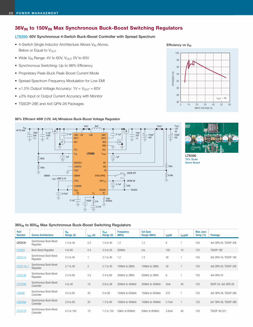
36VIN to 150VIN Max Synchronous Buck-Boost Switching Regulators
• 4-Switch Single Inductor Architecture Allows VIN Above,
Below or Equal to VOUT
• Wide VIN Range: 4V to 60V, VOUT 0V to 60V
• Synchronous Switching: Up to 98% Efficiency
• Proprietary Peak-Buck Peak-Boost Current Mode
• Spread Spectrum Frequency Modulation for Low EMI
• ±1 .5% Output Voltage Accuracy: 1V = VOUT = 60V
• ±3% Input or Output Current Accuracy with Monitor
• TSSOP-28E and 4x5 QFN-28 Packages
LT8390: 60V Synchronous 4-Switch Buck-Boost Controller with Spread Spectrum
98% Efficient 48W (12V, 4A) Miniature Buck-Boost Voltage Regulator
Efficiency vs VIN
165k
0.1µF
4.7µF
4mΩ
0.1µF
6uH
22µF
383k
4.7µF100k
0.47µF
100k
4.7nF
27k
100k
9.09k
15mΩ
10µF25V×2
0.1µF
1µF 1µF
100pF
120µF16V
120µF16V
EN/UVLO
VREF
CTRL
PGOOD
BG2
BST2
TG2
INTV CC
LOADEN
FB
VOUT
ISP
ISN
SYNC/SPRD
TEST
V IN4V TO 56V
400kHz
63V×2
100V×2
ISMON
PGOOD
VOUT12V4A
LSP LSNSW1 SW2BST1
TG1
BG1
V IN LT8390
LOADTG
ISMON
SS VC RT
GND
SSFM OFF
SSFM ONIOUT LIMIT 6.7A
36VIN to 80VIN Max Synchronous Buck-Boost Switching Regulators
Part Number Device Architecture
VIN Range (V) IOUT (A)
VOUT Range (V)
Frequency (MHz)
Ext Sync Range (MHz) IQ(µA) ISD(µA)
Max Junc Temp (˚C) Package
LTC3131 Synchronous Buck-Boost Regulator
1.5 to 40 0.2 1.0 to 40 1.2 1.2 6 1 150 4x4 QFN-20, TSSOP-20E
LT3433 Buck-Boost Regulator 4 to 60 0.4 3.3 to 20 200kHz n/a 100 10 125 TSSOP-16E
LTC3114Synchronous Buck-Boost Regulator
2.2 to 40 1 2.7 to 40 1.2 1.2 30 1 150 3x5 DFN-16, TSSOP-16E
LTC3115/-1Synchronous Buck-Boost Regulator
2.7 to 40 2 2.7 to 40 100kHz to 2MHz 100kHz to 2MHz 30 1 150 4x5 DFN-20, TSSOP-20E
LTC3136Synchronous Buck-Boost Regulator
2.4 to 60 2.5 2.4 to 60 200kHz to 2MHz 200kHz to 2MHz 6 1 150 4x4 DFN-24
LTC3789Synchronous Buck-Boost Controller
4 to 40 10 0.8 to 38 200kHz to 400kHz 200kHz to 400kHz 3mA 40 125 SSOP-24, 4x5 QFN-28
LT8390Synchronous Buck-Boost Controller
4.0 to 60 20 0 to 60 150kHz to 650kHz 150kHz to 650kHz 270 1 150 4x5 QFN-28, TSSOP-28E
LT8705ASynchronous Buck-Boost Controller
2.8 to 80 20 1.3 to 80 100kHz to 400kHz 100kHz to 400kHz 2.7mA 1 125 5x7 QFN-38, TSSOP-38E
LTC3779Synchronous Buck-Boost Controller
4.5 to 150 10 1.2 to 150 50kHz to 600kHz 50kHz to 600kHz 3.6mA 40 150 TSSOP-38 (31)
IOUT = 4A
INPUT VOLTAGE (V)0 10 20 30 40 50 60
86
88
90
92
94
96
98
100
EFFI
CIEN
CY (%
)
LT8390 75% Scale Demo Board

2 1P O W E R M A N A G E M E N T
Monolithic Step-Up DC/DC Converters
• 3V to 40V Input Voltage Range
• 1A, 60V Power Switch
• IQ < 6µA
• Fixed 2MHz Switching Frequency
• Positive or Negative Output Voltage Programming
• SOT-23-5 or 2x3 DFN-8 Package
LT8330: Low IQ Boost/SEPIC/Inverting Converter with 1A, 60V Switch
48V Boost Converter Efficiency and Power Loss
4.7µF
34.8k
4.7µF
1µF
4.7pF
V IN SW
FBXGND
EN/UVLO
LT8330
VIN12V
6.8µH VOUT48V135mA
VCCINT
1M
EFFICIENCYPOWER LOSS
LOAD CURRENT (mA)0 40 80 120 160
0
10
20
30
40
50
60
70
80
90
100
0
100
200
300
400
500
600
700
800
900
1000
EFFI
CIEN
CY (%
)
POWER LOSS (m
W)
High Voltage—Outputs to 140V
Part Number Device Architecture
VIN Range (V)
VOUT (MAX)(V) ISW (A)
Frequency (MHz) IQ(µA) ISD(µA)
Max Junc Temp (˚C) Package
LT3461/A Boost 2.5 to 16 38 0.30 1.3/3 2.8 1 125 ThinSOT
LT3460 Boost 2.5 to 16 36 0.32 1.3 2.0 1 125 SC70, ThinSOT
LT1945 Boost 1 to 15 36 0.35 COT 20μA 1 125 MSOP-10
LT8331 Boost 4.5 to 100 140 0.50 100kHz to 500kHz 6µA 1 125 HV MSOP-16E
LT3495/B/B-1 Boost 2.3 to 16 40 0.65/0.35 LNAPC 60µA 1 125 2x3 DFN-10
LT1930/A Boost 2.6 to 16 36 1.00 1.2/2.2 4.2/5.5 1 125 ThinSOT
LT8330 Boost 2.7 to 40 65 1.00 2 6µA 1 150 3x3 DFN-8, MSOP-8
LT8580 Boost 2.55 to 40 65 1.00 200kHz to 1.5MHz 1.2 1 150 2x3 DFN-8, SOT-23-8
LT3467 Boost 2.4 to 16 40 1.10 1.3 1.0 1 125 ThinSOT
LT1946/A Boost 2.45 to 16 35 1.50 2.7 3.6 1 125 MSOP-8E
LT1618 Boost 1.6 to 18 36 1.50 1.4 1.8 1 125 MSOP-10
LT3580 Boost 2.5 to 32 42 2.00 200kHz to 2.5MHz 1.0 1 150 3x3 DFN-8, MSOP-8
LT8335 Boost 2.7 to 25 28 2.00 2 6µA 1 150 3x3 DFN-8,
LT8582 Boost 2.5 to 22, 40V Max 42 3.00 200kHz to 2.5MHz 2.1 1 125 4x7 QFN-24
LT3581 Boost 2.5 to 22, 40V Max 42 3.30 200kHz to 2.5MHz 1.9 1 125 3x4DFN-14, MSOP-16E
LT3956 Boost 4.5 to 80 84 3.30 100KHz to 1MHz 1.6 1 125 5x6 QFN-36
LT3958/A Boost 5 to 80 84 3.30 100KHz to 1MHz 1.6 1 125 5x6 QFN-36
LT8741 Boost, Buck 2.6 to 50 50 2 x 2A 100KHz to 2MHz 70μA 1 125 TSSOP-20E
LT3957/A Boost 3 to 40 40 5.00 100KHz to 1MHz 1.7 1 125 5x6 QFN-36
LT3579/-1 Boost 2.5 to 16, 40V Max 42 6.00 200kHz to 2.5MHz 1.9 1 125 4x5 QFN-20, TSSOP-20E
LT8330 Actual Size Demo Board

P O W E R M A N A G E M E N T2 2
+–
100µA
IN
EN/UV
PG
GND
OUT
LT3045
ILIM PGFB
402k10µF
4.7µF*
*OPTIONAL, SEE DATA SHEET
VIN5V ±5%
200k
4.7µF
VOUT3VIOUT(MAX)500mA
49.9k249Ω
30.1k
SET
OUTS
Low Noise LDOs
• Ultralow RMS Noise: 0 .8μVRMS (10Hz to 100kHz)
• Ultralow Spot Noise: 2nV/√Hz at 10kHz
• Ultrahigh PSRR: 76dB at 1MHz
• Output Current: 500mA
• Wide Input Voltage Range: 1 .8V to 20V
• Single Capacitor Improves Noise and PSRR
• 100μA SET Pin Current: ±1% Initial Accuracy
LT3045: 20V, 500mA, Ultralow Noise, Ultrahigh PSRR Linear Regulator
LT3045 75% Scale Demo Board
Low Noise LDOs: Negative Regulators
Part Number
Device Architecture
VIN Range (V) IOUT (A) VOUT(MIN)(V)
Dropout Voltage (V)
Noise (µVRMS) IQ(µA) ISD(µA) Output Voltage (V)
Max Junc Temp (˚C) Package
LT1964 Single -1.9 to -20 200mA -1.21 0.34 30 30 3 Adj, -5 125 ThinSOT
LT3032 Dual ±1.9 to ±20 150mA/150mA ±1.22 0.30/0.34 20/30 55 <1 Adj, ±5 125 3x4 DFN-14
LT1175 Single -4.3 to -20 500mA -3.8 0.50 n/a 45 10 Adj, -5 125 DD, SOT-223, SO-8, PDIP8
LT3090 Single -1.5 to -36 600mA 0 0.3 18 1mA <1 Adj (0 to -32) 150 3x3 DFN-12, MSOP-12E
LT3091 Single -1.5 to -36 1.5A 0 0.3 18 1.2mA <1 Adj (0 to -32) 1504x3 DFN-14, DDPAK-7, TO-220, TSSOP-16E
LT3015 Single -1.9 to -30 1.5A -1.22 0.34 60 1.2mA <1Adj (–1.22V to –29.3V), Fixed
1253x3 DFN-8, MSOP-12E, DD-Pak, TO-220
LT1185 Single -4.3 to -35 3A -2.40 0.80 n/a 2.5mA 1 Adj 125 T0–220
5V to 3.3V Ultralow Noise LDO Regulator
2 3P O W E R M A N A G E M E N T
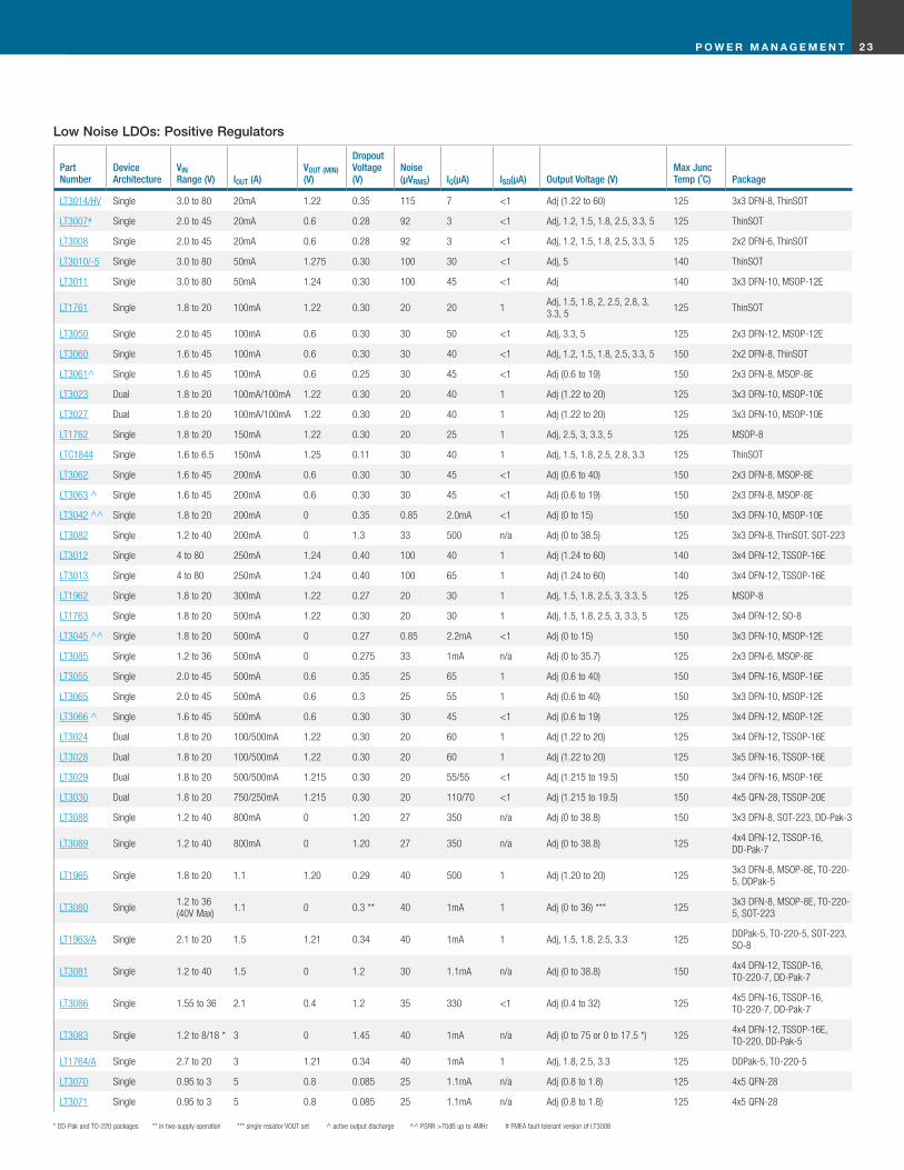
Low Noise LDOs: Positive Regulators
Part Number
Device Architecture
VIN Range (V) IOUT (A)
VOUT (MIN)(V)
Dropout Voltage (V)
Noise (μVRMS) IQ(µA) ISD(µA) Output Voltage (V)
Max Junc Temp (˚C) Package
LT3014/HV Single 3.0 to 80 20mA 1.22 0.35 115 7 <1 Adj (1.22 to 60) 125 3x3 DFN-8, ThinSOT
LT3007# Single 2.0 to 45 20mA 0.6 0.28 92 3 <1 Adj, 1.2, 1.5, 1.8, 2.5, 3.3, 5 125 ThinSOT
LT3008 Single 2.0 to 45 20mA 0.6 0.28 92 3 <1 Adj, 1.2, 1.5, 1.8, 2.5, 3.3, 5 125 2x2 DFN-6, ThinSOT
LT3010/-5 Single 3.0 to 80 50mA 1.275 0.30 100 30 <1 Adj, 5 140 ThinSOT
LT3011 Single 3.0 to 80 50mA 1.24 0.30 100 45 <1 Adj 140 3x3 DFN-10, MSOP-12E
LT1761 Single 1.8 to 20 100mA 1.22 0.30 20 20 1Adj, 1.5, 1.8, 2, 2.5, 2.8, 3, 3.3, 5
125 ThinSOT
LT3050 Single 2.0 to 45 100mA 0.6 0.30 30 50 <1 Adj, 3.3, 5 125 2x3 DFN-12, MSOP-12E
LT3060 Single 1.6 to 45 100mA 0.6 0.30 30 40 <1 Adj, 1.2, 1.5, 1.8, 2.5, 3.3, 5 150 2x2 DFN-8, ThinSOT
LT3061^ Single 1.6 to 45 100mA 0.6 0.25 30 45 <1 Adj (0.6 to 19) 150 2x3 DFN-8, MSOP-8E
LT3023 Dual 1.8 to 20 100mA/100mA 1.22 0.30 20 40 1 Adj (1.22 to 20) 125 3x3 DFN-10, MSOP-10E
LT3027 Dual 1.8 to 20 100mA/100mA 1.22 0.30 20 40 1 Adj (1.22 to 20) 125 3x3 DFN-10, MSOP-10E
LT1762 Single 1.8 to 20 150mA 1.22 0.30 20 25 1 Adj, 2.5, 3, 3.3, 5 125 MSOP-8
LTC1844 Single 1.6 to 6.5 150mA 1.25 0.11 30 40 1 Adj, 1.5, 1.8, 2.5, 2.8, 3.3 125 ThinSOT
LT3062 Single 1.6 to 45 200mA 0.6 0.30 30 45 <1 Adj (0.6 to 40) 150 2x3 DFN-8, MSOP-8E
LT3063 ^ Single 1.6 to 45 200mA 0.6 0.30 30 45 <1 Adj (0.6 to 19) 150 2x3 DFN-8, MSOP-8E
LT3042 ^^ Single 1.8 to 20 200mA 0 0.35 0.85 2.0mA <1 Adj (0 to 15) 150 3x3 DFN-10, MSOP-10E
LT3082 Single 1.2 to 40 200mA 0 1.3 33 500 n/a Adj (0 to 38.5) 125 3x3 DFN-8, ThinSOT, SOT-223
LT3012 Single 4 to 80 250mA 1.24 0.40 100 40 1 Adj (1.24 to 60) 140 3x4 DFN-12, TSSOP-16E
LT3013 Single 4 to 80 250mA 1.24 0.40 100 65 1 Adj (1.24 to 60) 140 3x4 DFN-12, TSSOP-16E
LT1962 Single 1.8 to 20 300mA 1.22 0.27 20 30 1 Adj, 1.5, 1.8, 2.5, 3, 3.3, 5 125 MSOP-8
LT1763 Single 1.8 to 20 500mA 1.22 0.30 20 30 1 Adj, 1.5, 1.8, 2.5, 3, 3.3, 5 125 3x4 DFN-12, SO-8
LT3045 ^^ Single 1.8 to 20 500mA 0 0.27 0.85 2.2mA <1 Adj (0 to 15) 150 3x3 DFN-10, MSOP-12E
LT3085 Single 1.2 to 36 500mA 0 0.275 33 1mA n/a Adj (0 to 35.7) 125 2x3 DFN-6, MSOP-8E
LT3055 Single 2.0 to 45 500mA 0.6 0.35 25 65 1 Adj (0.6 to 40) 150 3x4 DFN-16, MSOP-16E
LT3065 Single 2.0 to 45 500mA 0.6 0.3 25 55 1 Adj (0.6 to 40) 150 3x3 DFN-10, MSOP-12E
LT3066 ^ Single 1.6 to 45 500mA 0.6 0.30 30 45 <1 Adj (0.6 to 19) 125 3x4 DFN-12, MSOP-12E
LT3024 Dual 1.8 to 20 100/500mA 1.22 0.30 20 60 1 Adj (1.22 to 20) 125 3x4 DFN-12, TSSOP-16E
LT3028 Dual 1.8 to 20 100/500mA 1.22 0.30 20 60 1 Adj (1.22 to 20) 125 3x5 DFN-16, TSSOP-16E
LT3029 Dual 1.8 to 20 500/500mA 1.215 0.30 20 55/55 <1 Adj (1.215 to 19.5) 150 3x4 DFN-16, MSOP-16E
LT3030 Dual 1.8 to 20 750/250mA 1.215 0.30 20 110/70 <1 Adj (1.215 to 19.5) 150 4x5 QFN-28, TSSOP-20E
LT3088 Single 1.2 to 40 800mA 0 1.20 27 350 n/a Adj (0 to 38.8) 150 3x3 DFN-8, SOT-223, DD-Pak-3
LT3089 Single 1.2 to 40 800mA 0 1.20 27 350 n/a Adj (0 to 38.8) 1254x4 DFN-12, TSSOP-16, DD-Pak-7
LT1965 Single 1.8 to 20 1.1 1.20 0.29 40 500 1 Adj (1.20 to 20) 1253x3 DFN-8, MSOP-8E, TO-220-5, DDPak-5
LT3080 Single1.2 to 36 (40V Max)
1.1 0 0.3 ** 40 1mA 1 Adj (0 to 36) *** 1253x3 DFN-8, MSOP-8E, TO-220-5, SOT-223
LT1963/A Single 2.1 to 20 1.5 1.21 0.34 40 1mA 1 Adj, 1.5, 1.8, 2.5, 3.3 125DDPak-5, TO-220-5, SOT-223, SO-8
LT3081 Single 1.2 to 40 1.5 0 1.2 30 1.1mA n/a Adj (0 to 38.8) 1504x4 DFN-12, TSSOP-16, TO-220-7, DD-Pak-7
LT3086 Single 1.55 to 36 2.1 0.4 1.2 35 330 <1 Adj (0.4 to 32) 1254x5 DFN-16, TSSOP-16, TO-220-7, DD-Pak-7
LT3083 Single 1.2 to 8/18 * 3 0 1.45 40 1mA n/a Adj (0 to 75 or 0 to 17.5 *) 1254x4 DFN-12, TSSOP-16E, TO-220, DD-Pak-5
LT1764/A Single 2.7 to 20 3 1.21 0.34 40 1mA 1 Adj, 1.8, 2.5, 3.3 125 DDPak-5, TO-220-5
LT3070 Single 0.95 to 3 5 0.8 0.085 25 1.1mA n/a Adj (0.8 to 1.8) 125 4x5 QFN-28
LT3071 Single 0.95 to 3 5 0.8 0.085 25 1.1mA n/a Adj (0.8 to 1.8) 125 4x5 QFN-28
* DD-Pak and TO-220 packages ** in two-supply operation *** single resistor VOUT set ^ active output discharge ^^ PSRR >70dB up to 4MHz # FMEA fault tolerant version of LT3008

P O W E R M A N A G E M E N T2 4
GNDRUN
LTM8008
VINVIN
3V TO 72V
SS
SYNC
RT
VC
SPVVOUT1
VOUT2
VOUT3
VOUT4
VOUT5
VOUT6
INTVCC
3.3V AT 300mA
5V AT 150mA
5V AT 150mA
5V AT 150mA
5V AT 150mA
5V AT 500mA
SW
10µF SBR3U100LP-7
4.7µF
4.7µF
L1: COUPLED INDUCTOR, COILCRAFT MSD1278T-472ML
22µF
10µF
10µF
10µF
10µF
10µF22nF
42.2k 4.99k
L1A4.7µH
L1B4.7µH
Small Solutions with µModule Regulators
• One SEPIC Converter with Six Linear Regulators
• Wide Input Voltage Range: 3V to 72V, 6V Start
• 15mm × 15mm × 2 .82mm LGA Package
• Wide Temperature Range : –40°C to 150°C
LTM8008: 72VIN, 6 Outputs DC/DC SEPIC µModule Regulator
LTM8008 6-Output DC/DC µModuleCompared to Conventional Solutions, the LTM8008 Reduces Solution Size by 90%
µModule Regulators for Automotive
The highly integrated single and multiple output DC/DC µModule regulators
incorporate Linear Technology’s stringent design, manufacturing and
qualification disciplines . They address the need for compact and reliable
point-of-load voltage regulators in automotive applications such as driving
LEDs and powering an ECU (engine control unit) .
30mm
30mm
Part Number FunctionOutput Channel VIN Range VOUT Range IOUT
FMEA Comliant
Switching Frequency
Quiescent Current
Package Type Package Size (mm)
LTM8003Step-Down
Switching Regulator1 3.4V to 40V 0.97V to 18V
3.5A (Continuous),
6A (Peak)Yes 200kHz to 3MHz 25µA BGA 6.25 x 9 x 3.32
LTM8008 1 x SEPIC and 6 x LDOs 6 3V to 72V1 x 3.3V
5 x 5V
1 x 500mA (5V)
1 x 300mA (3.3)
4 x 150mA (5V)
No 100kHz to 1MHz 1.6mA LGA 15 x 15 x 2.82
LTM8005 LED Driver 1 5V to 38V 1.2V to 38V 1.6A No 100kHz to 1MHz 35µA BGA 9 x 11.25 x 2.22

2 5P O W E R M A N A G E M E N T
Small Solution Size
LTM8003: 150°C Operation, 40VIN, FMEA Compliant Step-Down µModule Regulator
• 6.25mm x 9mm x 3.32mm
• Load Dump: 42V VIN Abs Max
• Always On: 25μA IQ
• Cranking: 3.4V Start-Up Voltage
• EMI: CISPR 25 Class 5
• Reliability: FMEA Compliant (Fixed Voltage)
• Wide Temperature Range: -40°C to 150°C (H-Grade)
V(Battery)VIN: Up to 40V VOUT: 0.97V to 18V Low Voltage Switching
Regulators
LDOs
System Power
etc
etcCAN
ECU
Processor, CPU, FPGA
Memory
µModule DC/DC Regulator
LTM8003 75% Scale Demo Board
LTM8003 Typical Application. The LTM8003 Integrates an Inductor in the Package. Only 4 External Components Are Required.
4.7µF
47µF24.3k41.2k1MHz
LTM8003
VOUT
BIAS
VOUT5V3.5A6A PEAK
VINVIN7V TO 40V
FBGND
RUN
SYNC
RT

P O W E R M A N A G E M E N T2 6
LTM8003 Actual Size Demo Board
LTM8003 Typical Application. The LTM8003 Integrates an Inductor in the Package and Only 4 External Components Are Required.
FMEA Compliant Pinout, Low EMI µModule Regulators
LTM8003 Package Photo and Pin Configuration. The LTM8003 has FMEA Compliant Pinout (Fixed Voltage Version).
Part Number IOUT VIN Range VOUT RangeFMEA Comliant IQ
Switching Frequency
FMEA Compliant Pinout Package Size (mm)
LTM8003 3.5A (Continuous), 6A (Peak) 3.4V to 40V 0.97V to 18V Yes 25µA 200kHz to 3MHz Yes 6.25 x 9 x 3.32 BGA
4.7µF
47µF24.3k41.2k1MHz
LTM8003
VOUT
BIAS
VOUT5V3.5A6A PEAK
VINVIN7V TO 40V
FBGND
RUN
SYNC
RT
F
G
H
E
A
B
C
D
21 43 5 6
BGA PACKAGE48-LEAD (9mm × 6.25mm × 3.32mm) BGA PACKAGE
TOP VIEWFIXED OUTPUT VERSION
SYNC
GND
GND
RUN
NC
BIAS
BANK2VIN
PG
TR/SS
RT
GNDBANK 1
VOUTBANK 3

2 7P O W E R M A N A G E M E N T
Horizontal Polarization Average, with Spread Spectrum
Silent Switcher Low EMI µModule Regulators
Horizontal Polarization Average, without Spread Spectrum
Vertical Polarization Average, with Spread Spectrum
Vertical Polarization Average, without Spread SpectrumAM
PLIT
UDE
(dBµ
V/m
)
40
50
45
35
30
25
20
15
10
–15
–10
–5
5
0
FREQUENCY (MHz)
30 130 230 330 530430 630 730 830 930
CLASS 5 AVGWITH SS, AV V
AMPL
ITUD
E (d
BµV/
m)
40
50
45
35
30
25
20
15
10
–15
–10
–5
5
0
FREQUENCY (MHz)
30 130 230 330 530430 630 730 830 930
CLASS 5 AVGWITH SS, AV H
AMPL
ITUD
E (d
BµV/
m)
40
50
45
35
30
25
20
15
10
–15
–10
–5
5
0
FREQUENCY (MHz)
30 130 230 330 530430 630 730 830 930
CLASS 5 PEAKDATA
AMPL
ITUD
E (d
BµV/
m)
40
50
45
35
30
25
20
15
10
–15
–10
–5
5
0
FREQUENCY (MHz)
30 130 230 330 530430 630 730 830 930
CLASS 5 PEAKDATA
DC2416A EMI Performance in CISPR 25 Radiated Emission Test with and without Spread Spectrum (14VIN, IOUT = 3.5A). LTM8003 meets CISPR 25.
P O W E R M A N A G E M E N T2 8
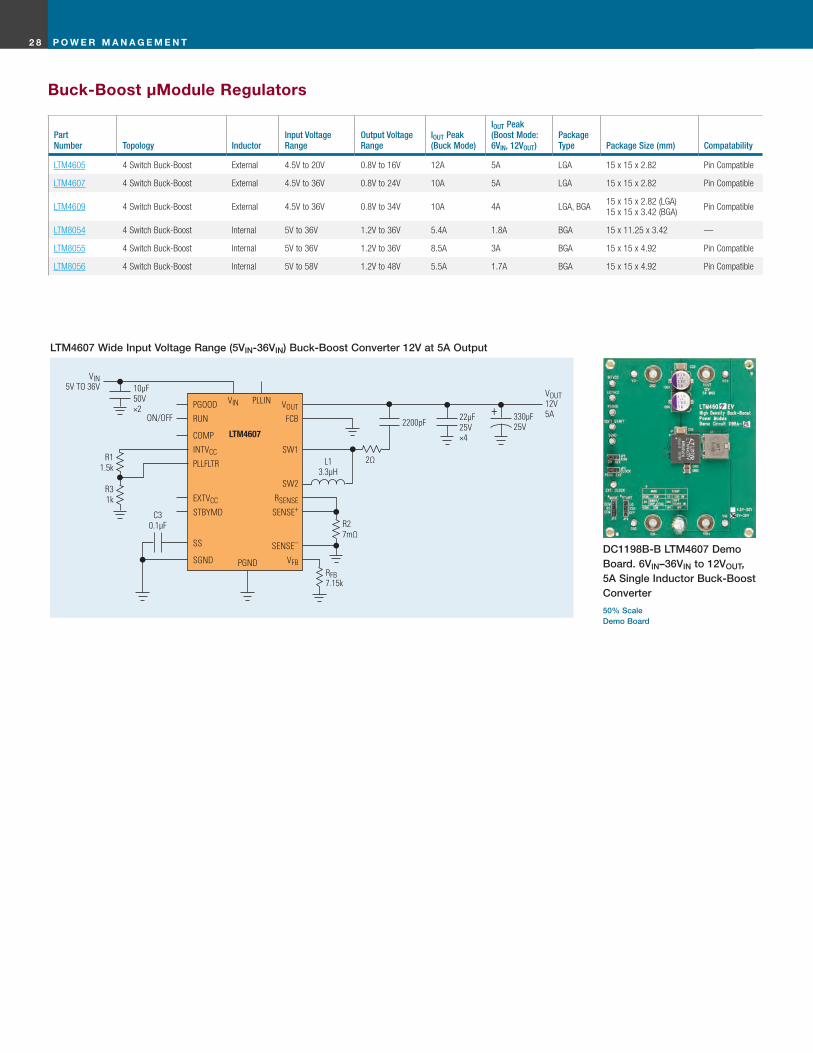
Part Number Topology Inductor
Input Voltage Range
Output Voltage Range
IOUT Peak (Buck Mode)
IOUT Peak (Boost Mode: 6VIN, 12VOUT)
Package Type Package Size (mm) Compatability
LTM4605 4 Switch Buck-Boost External 4.5V to 20V 0.8V to 16V 12A 5A LGA 15 x 15 x 2.82 Pin Compatible
LTM4607 4 Switch Buck-Boost External 4.5V to 36V 0.8V to 24V 10A 5A LGA 15 x 15 x 2.82 Pin Compatible
LTM4609 4 Switch Buck-Boost External 4.5V to 36V 0.8V to 34V 10A 4A LGA, BGA15 x 15 x 2.82 (LGA)15 x 15 x 3.42 (BGA)
Pin Compatible
LTM8054 4 Switch Buck-Boost Internal 5V to 36V 1.2V to 36V 5.4A 1.8A BGA 15 x 11.25 x 3.42 —
LTM8055 4 Switch Buck-Boost Internal 5V to 36V 1.2V to 36V 8.5A 3A BGA 15 x 15 x 4.92 Pin Compatible
LTM8056 4 Switch Buck-Boost Internal 5V to 58V 1.2V to 48V 5.5A 1.7A BGA 15 x 15 x 4.92 Pin Compatible
Buck-Boost µModule Regulators
LTM4607 Wide Input Voltage Range (5VIN-36VIN) Buck-Boost Converter 12V at 5A Output
DC1198B-B LTM4607 Demo Board. 6VIN–36VIN to 12VOUT, 5A Single Inductor Buck-Boost Converter
50% Scale Demo Board
VOUTPGOOD
FCBRUN
SW1
SW2
EXTVCC
STBYMD
SS
VFBSGND
PLLIN
LTM4607
RFB7.15k
22µF25V×4
330µF25V
VOUT12V5A
VIN
PGND
VIN5V TO 36V
C30.1µF
10µF50V×2 +
ON/OFF
COMP
INTVCC
RSENSE
SENSE–
PLLFLTR
R27mΩ
SENSE+
L13.3µH
2Ω
2200pF
R11.5k
R31k
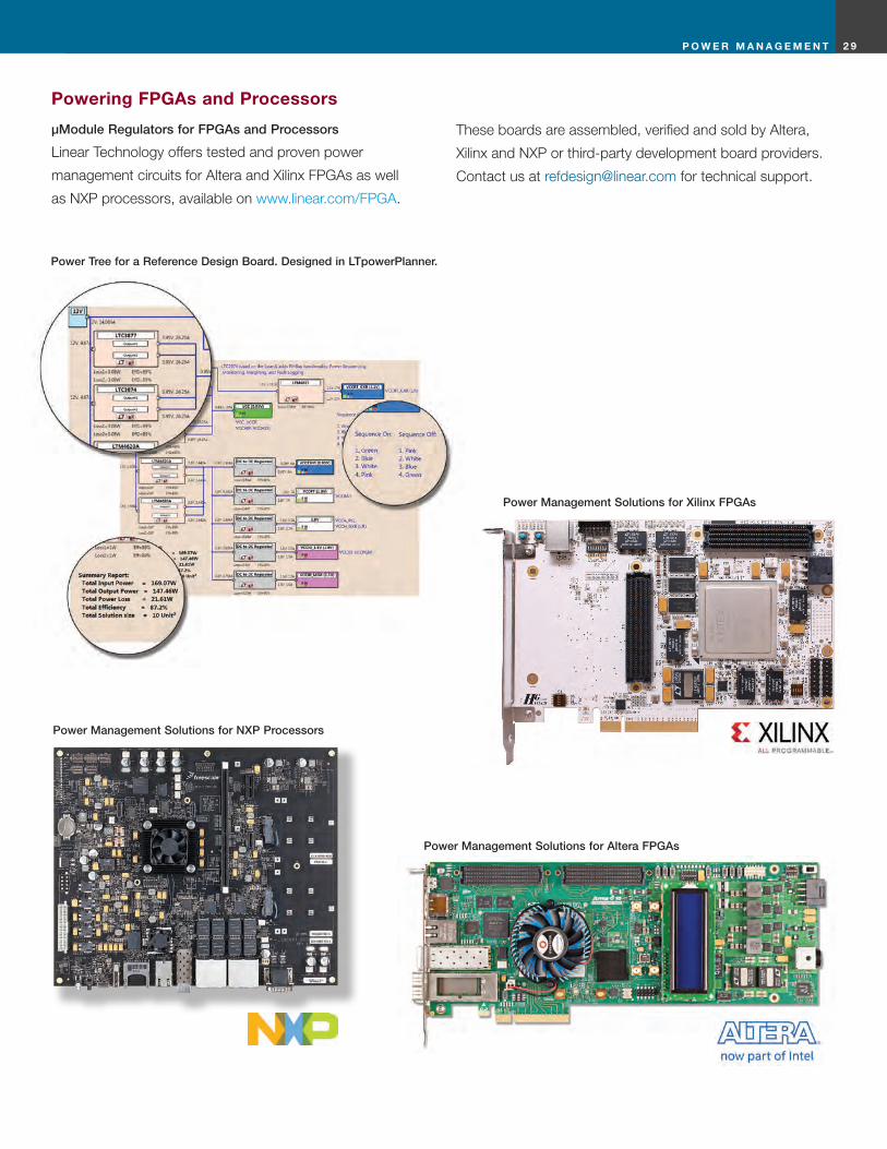
2 9P O W E R M A N A G E M E N T
Power Management Solutions for Xilinx FPGAs
Power Management Solutions for Altera FPGAs
µModule Regulators for FPGAs and Processors
Linear Technology offers tested and proven power
management circuits for Altera and Xilinx FPGAs as well
as NXP processors, available on www .linear .com/FPGA .
These boards are assembled, verified and sold by Altera,
Xilinx and NXP or third-party development board providers .
Contact us at refdesign@linear .com for technical support .
Powering FPGAs and Processors
Power Tree for a Reference Design Board. Designed in LTpowerPlanner.
Power Management Solutions for NXP Processors
B AT T E R Y M A N A G E M E N T3 0
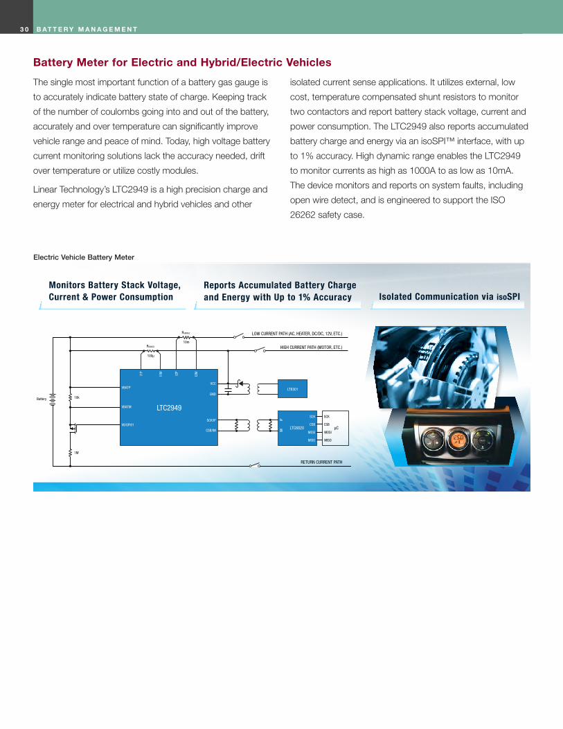
Electric Vehicle Battery Meter
The single most important function of a battery gas gauge is
to accurately indicate battery state of charge . Keeping track
of the number of coulombs going into and out of the battery,
accurately and over temperature can significantly improve
vehicle range and peace of mind . Today, high voltage battery
current monitoring solutions lack the accuracy needed, drift
over temperature or utilize costly modules .
Linear Technology’s LTC2949 is a high precision charge and
energy meter for electrical and hybrid vehicles and other
isolated current sense applications . It utilizes external, low
cost, temperature compensated shunt resistors to monitor
two contactors and report battery stack voltage, current and
power consumption . The LTC2949 also reports accumulated
battery charge and energy via an isoSPI™ interface, with up
to 1% accuracy . High dynamic range enables the LTC2949
to monitor currents as high as 1000A to as low as 10mA .
The device monitors and reports on system faults, including
open wire detect, and is engineered to support the ISO
26262 safety case .
Battery Meter for Electric and Hybrid/Electric Vehicles
Coulomb Counting for Battery Management Systems (BMS)
I2P
I2M
RSENSE2
10m
Battery 10kGND
VCC
HIGH CURRENT PATH (MOTOR, ETC.)
RETURN CURRENT PATH
LOW CURRENT PATH (AC, HEATER, DC/DC, 12V, ETC.)
VBATM
V8/GPI01
VBATP
SCK/IP
CSB/IM
I1P
I1M
100µ
RSENSE1
1M
LTC2949
IPIM
µCLTC6820
MISO MISO
MOSI MOSI
CSB CSB
SCK SCK
LT8301
Monitors Battery Stack Voltage, Current & Power Consumption
Reports Accumulated Battery Charge and Energy with Up to 1% Accuracy Is olated Communication via isoSPI

3 1B AT T E R Y M A N A G E M E N T
µC
Smar
tMes
h® W
irel
ess
BAT
TERY
-STA
CK
MO
NIT
OR
Smar
tMes
h® W
irel
ess
BAT
TERY
-STA
CK
MO
NIT
OR
Smar
tMes
h® W
irel
ess
BAT
TERY
-STA
CK
MO
NIT
OR
Smar
tMes
h® W
irel
ess
BAT
TERY
-STA
CK
MO
NIT
OR
Smar
tMes
h® W
irel
ess
BAT
TERY
-STA
CK
MO
NIT
OR
Smar
tMes
h® W
irel
ess
BAT
TERY
-STA
CK
MO
NIT
OR
Smar
tMes
h® W
irel
ess
BAT
TERY
-STA
CK
MO
NIT
OR
Smar
tMes
h® W
irel
ess
BAT
TERY
-STA
CK
MO
NIT
OR
Smar
tMes
h® W
irel
ess
BAT
TERY
-STA
CK
MO
NIT
OR
AN
TA
NT
AN
T
AN
TA
NT
AN
T
AN
TA
NT
AN
T
ANT
ANT
ANT
••••••••••
••••••••••••••••••••••
• • • • • • • • • • • • • • • • • • •
• • • • • • • • • • • • • • • • • •
• • • • • • • • • • • ••
••
•
••
••
••
••
••
••
••
••
••
••
• • • • • • • • • • • • •• • • • • • • • • • • • •
• • • • • • • • • • • • •• • • • • • • • • • • • •
• • • • • • • • • • • • •• • • • • • • • • • • • •
• • • • • • • • • • • • •• • • • • • • • • • • • •
• • • • • • • • • • • • • • • •
• • • • • • • • • • • • • • • •
• • • • • • • • • • • •
• • • • • • • • • • • •
• • • • • • • • • • • •
• • • • • • • • • • • •
• • • • • • • • • • • •
• • • • • • • • • • • • • •
Wireless BMS Architecture
LTC6811 Features:
• Measures 12 Battery Cells in Series
• Total Measurement Error: 1 .2mV Max
• Built-in Programmable 3rd Order Noise Filter
• Passive Cell Balancing with Programmable Timer
• Engineered for ISO 26262 Compliant Systems
SmartMesh Features:
• >99 .999% Reliability
• End-to-End Security and Data Encryption
• Precise Time Synchronization
• Self-Configuring and Self-Healing
– Bidirectional Network
The LTC6811 is a complete battery measuring device for hybrid/electric vehicles that can
measure up to 12 series-connected battery cell voltages with better than 0 .04% accuracy .
The Wireless BMS Architecture Concept combines the LTC6811 with the LTC5800 from
Linear’s SmartMesh wireless mesh networking product line . Field-proven in Industrial Internet
of Things (IoT) applications, SmartMesh embedded wireless networks deliver >99 .999%
reliable connectivity in harsh RF environments by employing path and frequency diversity . The
combination of these products enables a more reliable wireless battery management system
for the next generation of electric vehicles .
LTC6811 High Voltage Battery Stack Monitor + SmartMesh
ANT
SmartMesh® WirelessBATTERY-STACK MONITOR
B AT T E R Y M A N A G E M E N T3 2
806Ω
1.21k
IPA
IBIAS
IMA
ICMP
VM
LTC6811-1
120Ω
120Ω
120Ω
VREG
ISOMD
806Ω
1.21k
IPA
IBIAS
IMA
ICMP
VM
GND3
GND2
IPB
IMB
IPB
IMB
LTC6811-1
120Ω
120Ω
VREG
ISOMD
806Ω
1.21k
IPA
IBIAS
IMA
ICMP
VM
GND4
IPB
IMB
LTC6811-1 VREG
ISOMD
100nF
100nF
806Ω
1.21k
5V
LTC6820
120Ω
2k
IBIAS
ICMP
GND
SLOW
VDD
IP
IM
POL
MSTR
PHA
EN
MISO
MOSI
SCK
CS
VDDS5V
Hybrid electric and electric vehicles depend on battery stacks
of up to hundreds of cells to develop the power required
to drive the high performance electric motors . A battery
managements system provides real-time measurements
of each individual battery cell . These measurements must
be highly accurate to maximize usable battery capacity,
increase pack reliability, and ensure safety .
LTC6811: High Voltage Battery Stack Monitor
• Measures Up to 12 Battery Cells in Series
• 1 .2mV Maximum Total Measurement Error
• Stackable Architecture Supports 100s of Cells
• Built-In isoSPI Interface
– 1Mbps Isolated Serial Communication
– Uses a Single Twisted Pair, Up to 100 Meters
– Low EMI Susceptibility and Emissions
High Voltage Multicell Battery Stack Monitors
Communications—isoSPI
Measurement and Communications
isoSPI connects standard SPI devices using a single
twisted pair of wire up to 100 meters with full galvanic
isolation . The LTC6820 encodes SPI signals, up to 1Mbps,
into a differential signal that is transmitted across a simple
pulse transformer .

3 3B AT T E R Y M A N A G E M E N T
Active Battery Balancing ICs
Electric vehicles (EV) and plug-in hybrid vehicles (PHEV) are
demanding longer usable run time from their battery stacks .
These stacks of batteries are typically made of battery
modules, each with as many as 12 Li-Ion cells stacked in
series, offering a ~40V battery module . As the battery run time
defines the very feasibility of these vehicles, maximizing
battery capacity is of primary importance . Batteries can
always be made larger to improve driving range, but this
increases the weight, size and cost of the vehicle . So the
goal for automotive EV IC designers is to find ways to make
the existing batteries run longer . One effective method is to
employ active balancing .
LT8584: 2.5A Monolithic Active Cell Balancer with Telemetry Interface
• 2 .5A Typical Average Cell Discharge Current
• Integrated 6A/50V Power Switch
• Integrates Seamlessly with LTC680x Family (No Additional Software Required for “Simple Mode” Operation)
• Selectable Current and Temperature Monitors
• Ultralow Quiescent Current in Shutdown
• Engineered for ISO 26262 Compliant Systems
• Isolated Balancing:
– Can Return Charge to Top of Stack
– Can Return Charge to Any Combination of Cells in Stack
– Can Return Charge to 12V Battery for Alternator Replacement
• Can Be Paralleled for Greater Discharge Capability
• 16-Lead TSSOP Package
LTC3305: Lead Acid Battery 4-Cell Balancer
• Single IC Balances Up to Four 12V Lead Acid Batteries in Series
• All N-FET Design
• Stackable to Balance Larger Series Battery Packs
• Standalone Operation Requires No External µP or Control Circuitry
• Balancing Current Limited by External PTC Thermistor
• 38-Lead TSSOP and 7mm x 7mm 48-Lead LQFP Packages
LTC3300-1/-2: High Efficiency/Addressable Bidirectional Multicell Battery Balancer
• Bidirectional Synchronous Flyback Balancing of Up to 6 Li-Ion or LiFePO4 Cells in Series
• Up to 10A Balancing Current (Set by External Components)
• Bidirectional Architecture Minimizes Balancing Time and Power Dissipation
• Up to 92% Charge Transfer Efficiency
• Stackable Architecture Enables >1000V Systems
• Uses Simple 2-Winding Transformers
• 1MHz Daisy-Chainable Serial Interface with 4-Bit CRC Packet Error Checking
• Numerous Fault Protection Features
• 48-Lead Exposed Pad QFN and LQFP Packages

L E D s3 4
High Efficiency LED Drivers
• 2 .8V to 36V Input Voltage Range
• Up to 34V LED String Voltage
• ±2% LED Current and Output Voltage Regulation
• ±2% Output Voltage Regulation
• 5000:1 External PWM Dimming, 128:1 Internal PWM Dimming
• Silent Switcher Architecture for Low EMI
• Spread Spectrum Frequency Modulation
• Operates in Boost, Buck Mode and Buck-Boost Mode
• 4x5 QFN-28 Package
2MHz, 93% Efficient 10W (30V, 333mA) Boost LED Driver
Efficiency vs VIN
VINVIN
8V TO 27V
365k
59.0k
100k
EN/UVLO
OVLO
VREF
CTRLANALOG DIM
PWM DIM PWM
SYNC/SPRD
INTVCC
FAULT
BSTSW
VOUT
VOUT
FB
RP VCRT
ISP
GND
GND
ISN
PWMTG
ISMON
LT3922
1M
1M
33.2k
100k
10k
1nF
1µF
0.1µFL1
4.7µH
M1
300mΩ
4.7µF
0.47µF
0.47µF
30V333mA
LED
SS
45.3k2MHz
2.2µF
10nF
4.7µF
VLED = 30V fSW = 2MHz
100% PWM Duty Cycle
V IN (V)6 9 12 15 18 21 24 27 30
70
75
80
85
90
95
100
EFFI
CIEN
CY (%
)
LT3922: 36V, 2A Synchronous Step-Up LED Driver
LT3922 Actual Size Demo Board

3 5L E D s
High Efficiency LED Drivers
Part Number Topology Dimming Type
Max # of LEDs X ILED from 12 VIN
LED Configuration
Input Voltage Range (V)
Max. Output Voltage (V) ISW (A)*
Frequency (MHz)
Over- Voltage Protection
Max Junc Temp (˚C) Package
LT3517 Buck, Boost, Buck/Boost 5000:1 PWM 20:1 Analog
4x 300mA Series3 to 30 (40MAX)
45 1.3250kHz to 2.5MHz
Yes 150 4x4 QFN-16, TSSOP-16E
LT3599 4-Channel Boost 3000:1 PWM 20:1 Analog
4 x 10 x 100mA
Four Parallel Strings
3 to 30 (36MAX)
44 2200kHz to 2.5MHz
Yes 150 5x5 QFN-32, TSSOP-28E
LT3518 Buck, Boost, Buck/Boost 5000:1 PWM 20:1 Analog
8x 300mA Series3 to 30 (40MAX)
45 2.3250kHz to 2.5MHz
Yes 150 4x4 QFN-16, TSSOP-16E
LT3922Silent Switcher Buck, Boost, Buck/Boost
128:1 Int PWM 5000:1 PWM 20:1 Analog
11x 320mA Series 3 to 36 40 2200kHz to 2MHz
Yes 150 4x5 QFN-28
LT3932 Silent Switcher Buck128:1 Int PWM 5000:1 PWM 20:1 Analog
3 X 2A Series 40 n/a 2200kHz to 2MHz
Yes 150 4x5 QFN-28
LT3478/-1 Buck, Boost, Buck/Boost 3000:1 PWM 6 x 1A Series2.8 to 36 (40MAX)
40 4.5200kHz to 2.25MHz
Yes 125 TSSOP-16E
LT3952 Buck, Boost, Buck/Boost 5000:1 PWM 20:1 Analog
7 x 1A Series 3 to 42 60 4.5200kHz to 3MHz
Yes 150 TSSOP-28E
LT3476Buck, Boost, Buck/Boost Quad
1000:1 PWM 4 x 8 x 350mA
4 x Mutiple Series String
2.8 to 16 36 4 x 1.5200kHz to 2MHz
Yes 125 5x7 QFN-38
LT3760 8-Channel Boost 3000:1 PWM 25:1 Analog
8 x 10 x 100mA
Eight Parallel Strings
6 to 40 45 Ext FET100kHz to 1MHz
Yes 125 TSSOP-28E
LT3754 16-Channel Boost 3000:1 PWM 25:1 Analog
16 x 10 x 50mA
Sixteen Parallel Strings
6 to 40 45 Ext FET100kHz to 1MHz
Yes 125 5x5 QFN-28
LT3761/ABuck, Boost, Buck/Boost LED Driver w/PWM
3000:1 PWM 20:1 Analog
14 x 1A Series 4.5 to 60 80 Ext FET100kHz to 1MHz
Yes 125 MSOP-16E
LT3797Triple Buck, Boost, Buck/Boost
3000:1 PWM 20:1 Analog
3 x 14 x 1A Series2.5 to 40, 60MAX
100 Ext FET100kHz to 1MHz
Yes 125 7x8 QFN-52
LT3795 Buck, Boost, Buck/Boost 3000:1 PWM 20:1 Analog
14 x 1A Series 6 to 100 100 Ext FET100kHz to 1MHz
Yes 125 TSSOP-28E
LT3796 Buck, Boost, Buck/Boost 3000:1 PWM 20:1 Analog
20 x 400mA Series 6 to 100 100 Ext FET100kHz to 1MHz
Yes 125 TSSOP-28E
LT8391 Synchronous Buck-Boost 128:1 Int PWM 2000:1 PWM 20:1 Analog
14 x 2A Series 4 to 60 60 Ext FET150kHz to 650kHz
Yes 125 TSSOP-28E 4x5 QFN-28
LT3755 Buck, Boost, Buck/Boost 3000:1 PWM 20:1 Analog
14 x 1A Series 4.5 to 40Limited By Ext. FET
Ext FET100kHz to 1MHz
Yes 150 3x3 QFN-16, MSOP-16E
LT3756 Buck, Boost, Buck/Boost3000:1 PWM 20:1 Analog
14 x 1A Series 6 to 100Limited By Ext. FET
Ext FET100kHz to 1MHz
Yes 150 3x3 QFN-16, MSOP-16E
LT3956Constant Current/Constant Voltage Converter
3000:1 PWM 20:1 Analog
18 x 0.35A Series 4.5 to 80 80 Ext FET100kHz to 1MHz
Yes 125 5x6 QFN-36
μModule LED Driver
Part Number Topology Dimming Type
Max # of LEDs X ILED from 12 VIN
LED Configuration
Input Voltage Range (V)
Max. Output Voltage (V) ISW (A)*
Frequency (MHz)
Over Voltage Protection
Max Junc Temp (˚C) Package
LTM8005 Boost 3000:1PWM 9x1.2A Series 5 to 38 38 12100kHz to 1MHz
Yes 1509x11.25x2.22 BGA

L E D s3 6
Matrix LED Dimmer Powered by a Buck Mode LED Driver
• Eight Independent 17V 330mΩ NMOS Switches
• Independent On/Off/Dimming Control of 1 to 4 LEDs for
Each Switch
• I2C Multidrop Serial Interface with Programmable Open
LED and Shorted LED Fault Reporting
• 16 Unique I2C Addresses
• VDD Range: 2 .7V to 5 .5V and VIN Range: 8V to 60V
• Digital Programmable 256:1 PWM Dimming
• Fade Transition Between PWM Dimming States
• Optional Internal Clock Generator or External Clock Source for
PWM Dimming
• Open LED Overvoltage Protection
• Flicker Free PWM Dimming
• TSSOP-28E Package
LT3965: 8-Switch Matrix LED Dimmer
L133µHD1
D2 D3
D4
D5
500mA
LED+
LED+
LED–
VLED26V
VIN40V
0.01µF
VIN ISP
0.5Ω
ISN
RT DIM/SS VC
LT3955
EN/UVLO
PWM
VREF
CTRL
PGND
INTVCC
PWMOUT
SYNC
VMODE
FB
GND
GNDK
SW
28.7k375kHz
VCC5V
SDA
SCL
ALERT
28k500Hz DIMMING FREQUENCY
L1: WURTH 744066330D1: DFLS260D2, D3: CMSD6263S 2 IN 1 PACKAGED4, D5: PMEG6010CEHM1: VISHAY Si7309DNQ1, Q3: ZETEX FMMT593Q2: ZETEX FMMT493
10k10k10k
1k
20k
1µF50V
2.2nF 1µF
0.1µF100V
0.1µF
28k
49.9k
EN/UVLO
BIAS
BIAS UVLO DETECT
BIAS
9.09k
1k
IN4148
Q1
M1
Q2750Ω
1k
GND
LT3965
VDD
EN/UVLO EN/UVLO
SDA
SCL
ALERT
RTCLK
ADDR1
ADDR2
ADDR3
ADDR4
LEDREF
DRN8
DRN7SRC8
DRN6SRC7
DRN5SRC6
DRN4SRC5
DRN3SRC4
DRN2SRC3
DRN1SRC2
SRC1
VIN
0.1µF
1µF100V
Q3
Matrix LED Dimmer
Any Brightness, Any Pattern with I2C Control

3 7L E D s
• Wide Input Voltage Range: 5V to 38V
• Adjustable LED Current Up to 1 .6A
• 40V Internal Power Switch
• Internal Spread Spectrum Frequency Modulation
• 3000:1 True Color PWM™ Dimming
• 9mm × 11 .25mm × 2 .22mm BGA Package
• Wide Temperature Range: –40°C to 150°C
LTM8005: 38VIN, 38VOUT Boost µModule LED Driver
LTM8005
EN/UVLO
OVLO
PWM
VREF
CTRL1
CTRL2
VOUT
ISN
LED
AUX
FB
ISMON
RAMPSS VC RT GND OPENLED SHORTLED
IVINPVIN IVINN SW DA
LEDSTRING
COUT2× 4.7µF50V
L8.2µH
100k
93.1k
1M
19.1k
4.7k 23.2kf = 350kHz
10nF
6.8nF
0.1µF
0.1µF
CIN2× 4.7µF50V
12.4k
374k
VIN 6V TO 27V
18.7k
LTM8005 350mA at 30.5V to 35.5V LED Strings from 6V to 27VIN (Boost)
LTM8005 50% Scale Demo Board

D ATA C O M M U N I C AT I O N S3 8
PoDL
Power over Data Line (PoDL) Kicks Automotive Ethernet into High Gear
The future of autonomously driven vehicles is around the next bend.
For ADAS and self-driving vehicles, data bandwidth is
becoming an increasing problem . To support video streaming
and machine analysis the vehicle communication backbone
needs to support data transfer rates on the order of 1Gbps
to avoid image degradation . Today the wiring harnesses
in vehicles support a mishmash of interface standards,
including proprietary standards like LVDS which can transmit
high speed data in one direction only, have limited support
for video inputs/outputs and utilize expensive STP or failure-
prone coaxial cabling . This situation has driven the industry
to define a new standard for automotive Ethernet, under
IEEE 802 .3bp, known as 1000BASE-T1 . This standard
utilizes a single unshielded twisted pair (UTP) and will be
able to transfer bidirectional data at up to 1Gbps while
meeting automotive EMC requirements .
High Bandwidth Automotive Ethernet Combined with PoDL Will Solve Many of Today’s Interconnectivity Challenges, Enabling a Fully Networked Vehicle, in Addition to Bringing Significant Weight and Cost Advantages.

3 9D ATA C O M M U N I C AT I O N S
Save Vehicle Weight and Cabling Cost Using UTP/PoDL
100Base-TXEthernet PHY
100Base-T1Ethernet PHY
Power Sourcing Equipment (PSE) Powered Device (PD)
15 meters UTP100Mbps data
plus power
100Base-T1Ethernet PHY
100Base-TXEthernet PHY
To further simplify connectivity, the IEEE taskforce (802 .3bu)
is finalizing the automotive industry’s version of Power over
Ethernet (PoE), to deliver power over the same twisted pair
as the data . This will be known as Power over Data Line
(PoDL), or “poodle,” and the standard is expected to be
ratified by early 2017 . PoDL simplifies the distribution of
power while also supporting the ISO 26262 safety case .
Since the number of Ethernet nodes may reach as high as
80 nodes in luxury vehicles by 2020, and as many as 40 in
standard vehicles, PoDL will significantly simplify the cabling .
PoDL is the essential technology to minimize vehicle weight,
cabling cost and footprint . Distributing power and data
over the same twisted pair provides the intrinsic benefits
of 100BASE-T1 and 1000BASE-T1 single twisted pair .
The twisted pair cable weight can be reduced by as much
as 30%, thus increasing fuel/battery economy . The wiring
harness is the third heaviest subsystem in a modern car .
UTP is easy to terminate, uses smaller connectors and is
significantly cheaper and more reliable than coax . Coax is at
a disadvantage when flexed, with an estimated lifetime of just
a few years .
Ethernet standardization ensures interoperability across all
vehicle sensor types, enabling car manufacturers to source
Ethernet PHYs and cables from multiple vendors . The
standard will support isochronous virtual paths, so latency
critical safety features can seamlessly share the network
with low priority streaming applications . Standardization
allows modularization, slashing design integration effort in an
increasingly competitive industry .
Linear Technology offers an end-to-end PoDL solution,
providing increased robustness from cable faults . Linear’s
complete PoDL application circuit meets stringent automotive
signal integrity, EMI, and noise immunity requirements .
IEEE 802 .3bu compliant PSE and PD solutions will be
available for sampling in late 2017 . 100BASE-TI Ethernet
PHYs and 1000BASE-TI PHYs are already sampling in
the industry .
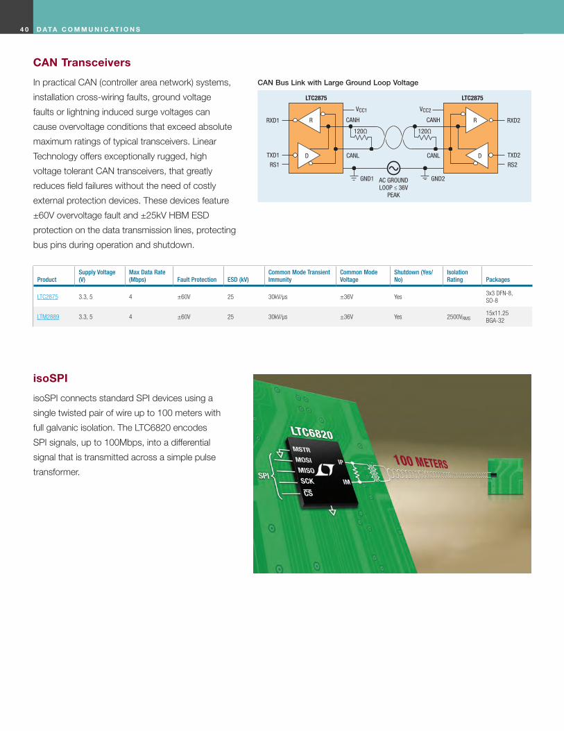
D ATA C O M M U N I C AT I O N S4 0
CAN Transceivers
isoSPI
In practical CAN (controller area network) systems,
installation cross-wiring faults, ground voltage
faults or lightning induced surge voltages can
cause overvoltage conditions that exceed absolute
maximum ratings of typical transceivers . Linear
Technology offers exceptionally rugged, high
voltage tolerant CAN transceivers, that greatly
reduces field failures without the need of costly
external protection devices . These devices feature
±60V overvoltage fault and ±25kV HBM ESD
protection on the data transmission lines, protecting
bus pins during operation and shutdown .
isoSPI connects standard SPI devices using a
single twisted pair of wire up to 100 meters with
full galvanic isolation . The LTC6820 encodes
SPI signals, up to 100Mbps, into a differential
signal that is transmitted across a simple pulse
transformer .
ProductSupply Voltage (V)
Max Data Rate (Mbps) Fault Protection ESD (kV)
Common Mode Transient Immunity
Common Mode Voltage
Shutdown (Yes/No)
Isolation Rating Packages
LTC2875 3.3, 5 4 ±60V 25 30kV/μs ±36V Yes3x3 DFN-8,SO-8
LTM2889 3.3, 5 4 ±60V 25 30kV/μs ±36V Yes 2500VRMS15x11.25BGA-32
120Ω
LTC2875
CANH
CANL
GND1 AC GROUNDLOOP ≤ 36V
PEAK
GND2
CANL
VCC1 VCC2
CANH
LTC2875
R
D
RXD1
TXD1
RS1
RXD2
TXD2
RS2
R
D
120Ω
CAN Bus Link with Large Ground Loop Voltage

4 1D ATA C O M M U N I C AT I O N S
Embedded chips and printed circuit boards with mesh networking software that deliver:
• >99.999% Data Reliability in the most challenging RF environments
• >10 Year Battery Life for every node in the network, including routing ones
• Complete Wireless Mesh Solution so no network stack development is required
Features:
• Self-Forming, Self-Sustaining, Multi-Hop Mesh Network
• Time Synchronized Channel Hopping (TSCH) link layer, pioneered by
Dust Networks®
– Channel Hopping on Each Transmission for frequency diversity
– Redundant Pathways for spatial diversity
– Low Power Packet Exchange—Duty cycle of <1% without sacrificing
network availability
– Zero In-Network Packet Collisions for a highly scalable network
• Built-In Network Optimization Algorithms fix problems before they occur
• 2 .4GHz IEEE 802 .15 .4 transceivers operate in globally license-free
2 .4GHz band
Benefits:
• Field Proven Network
– >50,000 customer networks
– >7 Billion hours of customer operation in harsh RF environments
• Highly Resilient, Low Power Communications in some of the most
demanding applications:
– Tough RF Environments with extensive metal and concrete, including
industrial plants, data centers, commercial building monitoring,
bridges, tunnels
– Networks on Moving Vehicles, including rail cars, cargo containers,
semi-trucks and aircraft
– Dense Deployments, where thousands of nodes operate within radio
range of each other, for instance rail yards, data centers, utility scale
solar farms
– Large Area Networks, such as shipyards, street parking applications
– Long, Extended Networks, including freight trains, pipelines,
mines, tunnels
– Remote Monitoring, where all nodes must be powered by battery or
energy harvesting, such as oil fields or environmental monitoring
• Place a sensor anywhere – no communications or power lines to wireless
nodes required
• Fast Time to Market
– Wireless network software is already complete, heavily tested and has
proven performance
– Hardware available as QFN chips or pre-certified PCB modules
SmartMesh—Embedded Wireless Sensor Networking
SmartMesh IP™ Motes and Managers are available as QFN chips and as pre-certified Printed Circuit Boards
Deployed in thousands of rail cars, SmartMesh® networks ensure reliable wireless communications in mobile environments.
To learn more about SmartMesh Embedded Wireless
Sensor Mesh Networks, visit www.linear.com/dust.

S I G N A L C H A I N4 2
+
–LTC6268-10
2.5V
PARASITIC FEEDBACK C2.5V
PD
–2.5V
VOUT = –IPD • 20kBW = 210MHz
PD = OSI OPTOELECTRONICS, FCI-125G-006
20kΩ
IPD
Radar and Lidar
Collision avoidance systems require high speed, low noise
amplifiers to scale and buffer sensor signals such as lidar
and radar . Linear Technology provides a range of products
including the LTC6268 and LTC6253 and differential output
amplifiers such as LTC6400-26 to enable next generation
ADAS systems . We also offer a full range of high performance,
low power, high speed ADCs which can be screened for
higher operating temperatures and AEC-Q100 qualified .
PLL Synthesizers
Features:
• 6GHz-Plus Frequency Generation
• Low –226dBc/Hz Normalized In-Band Phase Noise Floor
• –157dBc/Hz Wideband Output Phase Noise Floor
• –274dBc/Hz Normalized In-Band 1/f Noise
• Excellent Spurious Performance
• Integer-N or Fractional-N
Applications:
• Infotainment/GPS
• Satellite Uplink
• Femtocell
• Anti-Collision
PLL Synthesizer Snapshot
Phase Noise @ fRF=900MHz
Part Number FeaturesFrequency Range (GHz) 1MHz 40MHz
Spurious Products Vcc
Maximum Case Temperature Package
LTC6945 Integer-N PLL 0.350 to 6 –155dBc/Hz –161dBc/Hz –103dBc 3.3V/5V 105°C 4x5 QFN-28
LTC6946 Integer-N PLL + VCO 0.373 to 5.79 –141dBc/Hz –157dBc/Hz –102dBc 3.3V/5V 105°C 4x5 QFN-28
LTC6947 Frac-N PLL 0.350 to 6 –149dBc/Hz* –160dBc/Hz* –97dBc 3.3V/5V 105°C 4x5 QFN-28
LTC6948 Frac-N PLL + VCO 0.373 to 6.39 –140dBc/Hz –157dBc/Hz –98dBc 3.3V/5V 105°C 4x5 QFN-28
*At 2 .4GHz
LTC6948
VCO
REFDIV
OUTDIV
FRAC-N DIV∆∑ MOD

4 3S I G N A L C H A I N
Current Sense Amplifiers
Applications:
• H-Bridge Motor Control
• Solenoid Current Sense
• PWM Control Loops
• Hydraulic Controls
• Lamp Monitoring
• Glow Plug Control
• Load Monitoring
• HEV/EV Battery Management Systems
• 12V / 24V Battery Monitoring
• High Voltage Data Acquisition
• Remote Sensing
• Overcurrent and Fault Detection
• Cable Drop Compensation
• Fuse/MOSFET Monitoring
LT1999: High Voltage, Bidirectional Current Sense Amplifier
Features:
• Buffered Output with 3 Gain Options: 10, 20, 50
• Input Common Mode Voltage Range: –5V to 80V
• AC CMRR > 80dB at 100kHz
• Supply Range: 2 .7V to 36V, 44V Absolute Maximum
• –3dB Bandwidth: 2MHz
• Low Offset Voltage: 1 .5mV Maximum
• Smooth, Continuous Operation Over Entire Common Mode Range
• 4kV HBM Tolerant and 1kV CDM Tolerant
• Specified for –55°C to 150°C
• 8-Lead MSOP and 8-Lead SO (Narrow)
Part NumberCurrent Direction
Common Mode Voltage (V)
Response Time (μs)
VOS Max (μV)
PSRR Min (dB)
Max Temperature Range Comments
LT1999 Bidirectional –5 to 80 2.5 750 80 –55°C to 150°C High Speed AC Monitor, AC CMRR > 80dB at 100kHz
LT1997 Bidirectional ±160 50 98 –40°C to 125°C ±160V Common Mode Input Range
LT6375 Bidirectional ±270 300 101 –40°C to 125°C ±270V Common Mode Input Range, Diff Gain=1
LT1787 Bidirectional 2.5 to 65 10 150 100 –40°C to 125°C Buffered Output; Simple Input Filtering
LT6100 Unidirectional 4.1 to 48 40 300 95 –40°C to 125°C Buffered Output with 5 Gain Settings
LTC6101 Unidirectional 4.0 to 105 1 300 115 –40°C to 125°C Fast, High Voltage Monitor
LTC6102 Unidirectional 4.0 to 105 1 10 115 –40°C to 125°C Zero-Drift, Highest Precision
LTC6103 Unidirectional 4.0 to 70 1 450 106 –40°C to 125°C Dual Precision Amplifiers
LTC6104 Bidirectional 4.0 to 70 1 450 105 –40°C to 125°C Each Direction Gain Configurable
LT6105 Unidirectional –0.3 to 44 3.5 300 94 –40°C to 125°C Monitors Voltages Down to GND
LT6106 Unidirectional 2.7 to 44 3.5 250 106 –40°C to 125°C Lowest Cost, Simple
LT6107 Unidirectional 2.7 to 44 3.5 350 106 –55°C to 150°C Fully Tested at –55°C, 25°C, 150°C
LT6108 Unidirectional 2.7 to 60 3 125 120 –40°C to 125°C Includes Comparator+Ref
LT6109 Unidirectional 2.7 to 60 3 125 120 –40°C to 125°C Includes 2 Comparators+Ref
LT6110 Unidirectional 2.0 to 50 2 250 88 –40°C to 125°C Line Drop Compensator
LT6118 Unidirectional 2.7 to 60 3 200 120 –40°C to 125°C Includes Comparator with Power on Reset +Ref
LT6119 Unidirectional 2.7 to 60 3 200 120 –40°C to 125°C Includes Comparator with Power on Reset +Ref
LT1999
4k
0.8k
160k
160k
2µA
0.8k4k
SHDN
5V
V+
V+
V+5V
RS
+
–
+
–
VS
81
2
3
4
7
6
50.1µF
0.1µF
VOUT
RG
V+IN
V–IN
VREF
VSHDN
V+
V+
High AC Common Mode Rejection
Full Bridge Armature Current Monitor
TIME (10µs/DIV)
2.5V
V OUT
(2V/
DIV)
V+IN (20V/DIV)
VOUT
V+IN

S I G N A L C H A I N4 4
TimerBlox® Products
Features:
• Dedicated Timing Devices
– Includes Internal Silicon Oscillator
– Easily Programmed with Resistors
• ±20mA Output Current
• 60μA to 250μA Supply Current
• 2 .25V to 5 .5V Single Supply Operation
• Small Size: SOT-23, 2 x 3mm DFN
• Fast Start-Up
• Immune to Shock & Vibration
• Specified from –55°C to 125°C
TimerBlox Board 50% Scale Demo Board
LTC6992-1
MOD
GND
SET
OUT
V+
DIV
5VD1
HIGH INTENSITY LED
R2280kRSET
105k
VDIMMING
R11M
R390.9Ω
C10.1µF
LED Dimming via Direct PWM Control
LTC6990
OE
GND
SET
OUT
V+
DIV
1M
523k21.5k
5V
fOUT
5V
60.4k
Temperature to Frequency Converter
Hardware Watchdog Timer
Part Number Function Operating Range Package Details
LTC6990 Voltage-Controlled Oscillator (VCO) 488Hz to 1MHz SOT-23, DFN Simple and Flexible Control
LTC6991 Low Frequency Clock 29μHz to 488Hz SOT-23, DFN Period from 2 msec Up to 9.5 Hrs
LTC6992-1 Pulse-Width Modulation (PWM) 3.8Hz to 1MHz SOT-23, DFN 0% to 100% Pulse Width Control
LTC6992-2 Pulse-Width Modulation (PWM) 3.8Hz to 1MHz SOT-23, DFN 5% to 95% Pulse Width Control
LTC6992-3 Pulse-Width Modulation (PWM) 3.8Hz to 1MHz SOT-23, DFN 0% to 95% Pulse Width Control
LTC6992-4 Pulse-Width Modulation (PWM) 3.8Hz to 1MHz SOT-23, DFN 5% to 100% Pulse Width Control
LTC6993-1 One-Shot Circuit 1µs to 34s SOT-23, DFN Rising Edge Trigger
LTC6993-2 One-Shot Circuit 1µs to 34s SOT-23, DFN Rising Edge Trigger, Retriggerable
LTC6993-3 One-Shot Circuit 1µs to 34s SOT-23, DFN Falling Edge Trigger
LTC6993-4 One-Shot Circuit 1µs to 34s SOT-23, DFN Falling Edge Trigger, Retriggerable
LTC6994-1 Delay Block 1µs to 34s SOT-23, DFN Rising or Falling Edge Trigger
LTC6994-2 Delay Block 1µs to 34s SOT-23, DFN Rising & Falling Edge Trigger
LTC6995-1 Long Duration Power-On Reset 1.024 ms to 9.54 hours SOT-23, DFN Active High Reset, Selectable Polarity
LTC6995-2 Long Duration Power-On Reset 1.024 ms to 9.54 hours SOT-23, DFN Active Low Reset, Selectable Polarity
LTC6995
OUTPUT
FALLING EDGE TRIGGEREDPOL = 0
TRIGGER RST
GND
SET
OUT
V+
DIVRSET
R2
R1 0.1µF
V+

4 5S I G N A L C H A I N
Silicon Oscillators
Features:
• Simple Square Wave Oscillators
– No Crystal
– 1kHz to 170MHz Output Frequencies
• On-the-Fly Frequency Programmability
• Accuracy from 0 .1% to 1 .5%
• Low Power
• Small Size
• Fast Start-Up
• Immune to Shock & Vibration
• Specified from –55°C to 125°C
LTC6908: Dual Output Oscillator for Switching Regulators
Features:
• Two Options: Outputs
Complementary
(0°/180°) or Quadrature (0°/90°)
• Ideal for Switching Regulator
Phase Synchronization
• 50kHz to 10MHz Frequency Range
• One External Resistor Sets
the Frequency
• Optional Spread Spectrum
Modulation for Improved EMC
• 400µA Supply Current
• 260µs Start-Up Time
• Outputs Muted Until Stable
• Operates from a Single 2 .7V to
5 .5V Supply
• Available in Low Profile (1mm)
ThinSOT and DFN (2mm x 3mm)
Packages
Part Number
Frequency Output
Max Error (%)
Supply Current Package Features
LTC1799 1kHz to 33MHz 1.5 1mA @ 3MHz SOT-23 Frequency Set via 1 Resistor
LTC6903 1kHz to 68MHz 1.1 1.7mA @ 3MHz MSOP-8 Frequency Set via SPI Interface
LTC6904 1kHz to 68MHz 1.1 1.7mA @ 3MHz MSOP-8 Frequency Set via I2C Interface
LTC6905 17MHz to 170MHz 1.4 7mA @ 170MHz SOT-23 Frequency Set via 1 Resistor, 100µsec Startup
LTC6905-xx 20MHz to 133MHz 1.0 10mA @ 133MHz SOT-23 Pin Selectable Frequency
LTC6906 10kHz to 1MHz 0.5 60µA @ 1MHz SOT-23 Frequency Set via 1 Resistor, Very Low Power
LTC6907 40kHz to 4MHz 0.5 275µA @ 4MHz SOT-23 Frequency Set via 1 Resistor, Very Low Power
LTC6908 50kHz to 10MHz 1.5 400µA @ 50kHz SOT-23 2 Phase Output with Spread Spectrum Capability
LTC6909 50kHz to 10MHz 1.5 400µA @ 50kHz SOT-23 8 Phase Output with Spread Spectrum Capability
LTC6930 32.768kHz to 8.192MHz 0.09 400µA @ 50kHz MS8, DFN High Accuracy, Pin Selectable Frequency
CBYP
44.2k
OUT1
OUT2
fOUT = 10MHz • 10k/RSET
MOD
V+
GND
SET
SVIN TRACK
LTC3418RT
CIN100µF
0.2µH
LTC6908-1
RUN/SSITH
PGOOD
SW
PGNDSGND
SYNC/MODE VFB
PVIN
820pF
1000pF
CLOCK SIGNAL FOR REGULATOR #1 (0° PHASE)
CLOCK SIGNAL FOR REGULATOR #2 (180° PHASE)
0.1µFCOUT2 × 100µF(IN PARALLEL)
VOUT2.5V8A
4.32k
2k
41.2k2.2M
VIN2.8V TO 5.5V
4.99k
Dual Phase Clocking for 2 Switching Regulators
Spread Spectrum Frequency Modulation
10kHz TO 1MHz
NO DECOUPLINGCAPACITOR
NEEDED
RSET100k TO 1M
2.25V TO 3.6V
1310
V+
GND
DIV
OUT
GRD
SET
LTC6906
LTC6906 Micropower Clock Generator
9kHzRes BW
5dB/
DIV
Frequency(Fundamental and Third Harmonic Shown)
0 2 4 6 8

S I G N A L C H A I N4 6
Photodiode AmplifierPrecision Operational Amplifiers
Features:
• High Precision Over Temperature:
– I-Grade: –40°C to 85°C
– H-Grade: –40°C to 125°C
• Over-The-Top® (OTT) Inputs Allow Operation
with Input Voltages above V+
Single Part Number
Dual Part Number
Quad Part Number
VOS Max 25°C (μV)
TCVOS Max (μV/°C)
IB Max 25°C (nA)
GBW Typ 25°C (MHz)
en Typ 25°C (nV/√Hz)
IS Max 25°C (mA)
VS Range (V)
Rail-to-Rail I/O
Temperature Grade
LTC2054HV LTC2055HV 3 0.03 0.15 0.5 0.15 2.7 to 12 Out I, H
LTC2050HV LTC2051HV LTC2052HV 3 0.03 0.075 3 1.2 2.7 to 12 Out I, H
LTC2057 5 0.025 0.2 1.5 13 1.35 4.75 to 60 Out I, H
LTC1050 LTC1051 5 0.05 0.03 2.5 90 1.5 4.75 to 18 Out I, H
LTC6078 LTC6079 25 0.7 0.001 0.75 18 0.072 2.7 to 6 Yes I, H
LT6020 30 0.5 3 0.4 46 0.1 3 to 30 Out I, H
LT1028 40 0.8 90 75 0.85 9.5 8 to 44 I
LT6015 LT6016 LT6017 50 0.75 Typ 5 3.2 18 0.335 3 to 50 OTT I, H
LT1881 LT1882 50 0.8 0.2 1 14 0.9 2.4 to 40 Out I, H
LT1884 LT1885 50 0.8 0.4 2 9.5 0.9 2.4 to 40 Out I
LT6018 50 0.5 .50 15 1.2 7.65 8 to 33 Out I, H
LT6010 LT6011 LT6012 60 0.8 0.3 0.33 14 0.15 2.7 to 40 Out I
LT6020 70 0.3 3 0.4 46 0.1 3 to 35 Out I, H
LT6023 40 2.8 3 0.04 132 0.02 3 to 30 Out I, H
LTC6081 LTC6082 70 0.8 0.001 3.6 13 0.425 2.7 to 5.5 Yes I, H
LT1468 LT1469 75 2 40 90 5 5 9 to 36 I
LT1678 LT1679 100 3 20 20 3.9 3.4 3 to 36 Yes I
LTC6244 100 2.5 0.075 50 8 7.4 2.8 to 7 Out I, H
LTC6240 LTC6241 LTC6242 125 2.5 0.075 18 7 2.2 2.8 to 6 Out I, H
LT1013 LT1014 150 2 20 0.8 22 0.5 4 to 44 SS I
LT1880 150 1.2 0.9 1.1 13 1.9 2.4 to 40 Out I
LTC6360 250 30000 1000 2.3 17.5 4.75 to 5.25 Out I, H
LTC6255 LTC6256 LTC6257 350 3 60 6.5 20 0.073 1.8 to 5.25 Yes I, H
LT1637 LT1638 LT1639 350 3 50 1 27 0.25 1.8 to 44 OTT I, H
LT6220 LT6221 LT6222 350 5 150 60 10 1 2.2 to 12.6 Yes I
LT6233 LT6234 LT6235 350 3 3000 60 1.9 1.25 3 to 12.6 Out I
LT1800 LT1801 LT1802 350 5 250 80 8.5 2 2.3 to 12.6 Yes I
LT1494 LT1495 LT1496 375 2 1 0.0027 185 0.0015 2.1 to 36 OTT I, H
LT1722 LT1723 LT1724 400 7 300 200 3.8 4.5 4.6 to 12.6 I
LT6003 LT6004 LT6005 500 5 0.09 0.002 325 0.001 1.6 to 16 Yes I, H
LT1636 LT1490A LT1491A 500 4 8 0.18 50 0.055 2 to 44 OTT I, H
LT6202 LT6203 LT6204 500 24 7000 100 1.9 3.5 2.5 to 12.6 Yes I
LTC6246 LTC6247 LTC6248 500 350 180 4.2 1 2.5 to 5.25 Yes I, H
LT1806 LT1807 550 5 4000 325 3.5 13 2.5 to 12.6 Yes I
LT1351 LT1352 LT1353 600 8 50 3 14 0.33 5.0 to 36 I
LT1970 600 10 600 3.6 15 13 5 to 36 I
LT1357 LT1358 LT1359 600 8 500 25 8 2.5 5 to 36 I
LT6000 LT6001 LT6002 750 5 5 0.05 75 0.016 1.8 to 18 Yes I
LTC6084 LTC6085 750 5 0.04 1.5 27 0.13 2.5 to 5.5 Yes I, H
LTC6087 LTC6088 750 5 0.04 14 12 1.2 2.7 to 5.5 Yes I, H
LT1782 800 5 15 0.2 50 0.055 2.2 to 18 OTT I, H
LT1783 800 5 80 1.25 20 0.3 2.2 to 18 OTT I, H
LT1354 LT1355 LT1356 800 8 300 12 10 1.25 5 to 36 I
LTC6090 LTC6091 1000 5 0.05 12 14 3.9 9.5 to 140 Out I, H
Notes: Some parameters vary between single/dual/quad versions • For a complete list of products and full specifications visit www .linear .com • OTT=Over-The-Top Inputs
–2.5V
1M
3.8pFVOUT
2.5V
+
–
TEMD1000IR PHOTODIODE
AT 870nm (IR), VOUT = 600mV/μW RECEIVED POWER
1/2LTC6078

4 7S I G N A L C H A I N
Programmable Gain and Gain Selectable Amplifiers
Instrumentation Amplifiers
High Temp (125°C) Comparators
• High Precision Over Temperature:
– I-Grade: –40°C to 85°C
– H-Grade: –40°C to 125°C
• Integrated Resistors Simplify
Design
• High Precision Over Temperature:
– I-Grade: –40°C to 85°C
– H-Grade: –40°C to 125°C
• High Impedance Differential Inputs
• Fully Specified for –40°C to
125°C Operation
• High Voltage, Over-The-Top Inputs
• High Voltage, Open Collector Outputs
• High Sink Current Output
• Ideal for Level Translation
• Combination Parts Include:
– Internal Voltage Reference
– Current Sense Amplifiers
Part Number Channels
Gain Range
GBW (MHz)
Rail-to-Rail
Vs (V)
Is (mA)
Temperature Grade Features
LT1997-3 1 -13 to 14 1.4 IN/OUT 3.3 to 50 0.4 I, H ±160V Common Mode Range Selectable
LT6375 1 0.58 IN/OUT 3 to 50 0.4 I, H ±270V Common Mode Range Diff Amp
LTC6910 1 0 to 100 11 In/Out 2.7 to 10.5 3 I, H Programmable 3-Bit Digital Gain Control
LTC6911 2 0 to 100 11 In/Out 2.7 to 10.5 3 I, H Dual, Programmable Matched Channels
LTC6912 2 0 to 100 30 In/Out 2.7 to 10.5 2.75 I, H Dual, Programmable Independent Channels
LTC6915 1 0 to 4096 0.2 In/Out 2.7 to 11 1.6 I, H Zero-Drift PGA Instrumentation Amp
LT1991A 1 -13 to 14 0.56 Out 2.7 to 36 0.11 I, H Precision Pin-Configurable Diff Amp
LT1990A 1 1 to 10 0.1 Out 2.7 to 36 0.12 I, H ±250V Input Pin-Configurable Diff Amp
LT1995 1 -7 to 8 30 5 to 36 8.5 I High Speed Pin-Configurable Diff Amp
LT1996 1 -117 to 118 0.56 Out 2.7 to 36 0.11 I Precision Pin-Configurable Diff Amp
Part Number
Vos Max 25°C (µV)
Gain Error Max (%)
CMRR MIN (dB)
IB Max(nA) Vs (V)
Is (mA)
Temperature Grade Features
LTC2053 10 0.01 105 10 2.7 to 11 1.300 I, H Zero-Drift Instrumentation Amp
LT1167 40 0.02 126 0.35 4.6 to 40 1.300 I Precision Low Bias Current In Amp
LT1168 40 0.02 126 0.25 4.6 to 40 0.530 I Precision Power Current In Amp
LT1789 100 0.2 100 40 2.2 to 36 0.095 I Micropower Precision In Amp
LTC6915 10 0.075 105 10 2.7 to 11 1.600 I, H Zero-Drift PGA Instrumentation Amp
Part Number Channels
Internal Reference VS (V)
Max Input Voltage (V)
Max Output Voltage (V)
IS Max (μA)
Prop Delay (µS) Package
LT1716 1 No 2.7 to 44 44 VSUPPLY 50 9 SOT23
Comparator Combined with Voltage Reference
LT6700 2 400mV 1.4 to 18 18 18 15 18 SOT23, 2x3mm DFN
LT6700HV 2 400mV 1.4 to 18 18 36 15 18 SOT23, 2x3mm DFN
LT6703 1 400mV 1.4 to 18 18 18 11 18 SOT23, 2x2mm DFN
LT6703HV 1 400mV 1.4 to 18 18 36 11 18 SOT23, 2x2mm DFN
Comparator Combined with High Side Current Sense and Voltage Reference
LT6108-1 1 400mV 2.7 to 60 60 60 650 3 MSOP8, 2x3mm DFN
LT6108-2 1 400mV 2.7 to 60 60 60 650 3 MSOP8, 2x3mm DFN
LT6109 2 400mV 2.7 to 60 60 60 700 3 MSOP10
LT6118 1 400mV 2.7 to 60 60 60 650 3 MSOP8, 2x3mm DFN
LT6119 2 400mV 2.7 to 60 60 60 700 3 MSOP10
–
+
V+
V–
–15V
VSOURCE+ = –270V TO 270V
15V
OUTVOUT = ±10mV/mA
REF
–REFA
–IN
+IN
–REFB
19k 38k
190k
190k
190k
23.75k
–REFC
+REFA +REFB +REFC
19k 38k
SHDN
23.75k
RC10Ω
RSENSE10Ω
190k
LOAD
LT6375
±270V Input Common Mode Difference Amplifier
+
–
LTC2053
2
3
7
8
0.1µF
3V
R < 10K
1, 45
6R2 10K
OUT
0.1µFR110Ω
GAIN = 1+ R2R1
Differential Bridge Amplifier
S I G N A L C H A I N4 8
High Speed AmplifiersFeatures:
• High Gain Bandwidth Product and Slew Rate
• Fully Specified Over Temperature:
– I-Grade: –40°C to 85°C
– H-Grade: –40°C to 125°C
LTC6253: 720MHz, 3.5mA Power Efficient Rail-to-Rail I/O Op Amp
Features:
• Gain Bandwidth Product: 720MHz
• –3dB Frequency (AV = 1): 400MHz
• Low Quiescent Current: 3 .5mA Max
• High Slew Rate: 280V/μs
• Input Common Mode Range Includes Both Rails
• Output Swings Rail-to-Rail
• Low Broadband Voltage Noise: 2 .75nV/√Hz
• Power-Down Mode: 42μA
• Fast Output Recovery
• Supply Voltage Range: 2 .5V to 5 .25V
• Input Offset Voltage: 350μV Max
• Large Output Current: 90mA
Part Number Channels
GBW Typ 25°C (MHz)
Slew Rate Typ 25°C (V/μs)
VOS Max 25°C (μV)
IB Max 25°C (nA)
en Typ 25°C (nV/√Hz)
IS Max 25°C (mA)
VS Range (V)
Rail-to-Rail I/O
Temperature Grade
LTC6268-10LTC6269-10
1/2 4000 1000 700 0.00002 4 18 3.1 to 5.25 Out I, H
LTC6360 1 1000 135 250 30000 2.3 17.5 4.75 to 5.25 Out I, H
LTC6252/3/4 1/2/4 720 280 350 650 2.75 3.5 2.5 to 5.25 Yes I, H
LT6553/4 3 650 650 10000 50000 11 4.5 to 13.2 I
LT6555/6 3 650 650 16000 45000 12 4.5 to 12.6 I
LT6557/8 3 500 2200 40000 70000 25 3 to 7.5 I
LTC6268/9 1/2 500 400 700 0.00002 4.3 18 3.1 to 5.25 Out I, H
LT1818/9 1/2 400 2500 1500 8000 6 10 3.5 to 12.6 I
LT1395/6/7 1/2/4 400 800 12000 4.5 6.5 3 to 12.6 H
LT1806/7 1/2 325 125 550 4000 3 13 2.5 to 12.6 Yes I
LT1398/9 2/3 300 300 10000 50000 4.5 6.5 4 to 15.5 I
LT6552 1 300 2500 20000 50000 55 13.5 3 to 12.6 Out I
LT1815/6/7 1/2/4 220 1500 1500 8000 6 7.8 2.5 to 12.6 I
LT6230/1/2 1/2/4 215 70 500 10000 1 3.75 3 to 12.6 Out I
LT6210/1 1/2 200 700 6000 39000 6.5 8.3 3 to 13.2 Out I
LT6300/1 2/4 200 600 5000 4000 8 13.5 8 to 27 I
LT1722/3/4 1/2/4 200 70 400 300 3.8 4.5 4.6 to 12.6 I
LT1468-2/9-2 2/4 200 30 75 40 5 5 9 to 36 I
LTC6246/7/8 1/2/4 180 90 500 350 4.2 1 2.5 to 5.25 Yes I, H
LT6200/1 1/2 165 50 1000 40000 0.95 23 2.5 to 12.6 Yes I
LT1809/10 1/2 160 300 2500 8000 16 17 2.5 to 12.6 Yes I
LT6550/1 3/4 110 340 70000 65000 12 11 3 to 12.6 Out I
LT1812/3/4 1/2/4 100 750 1500 4000 8 3.6 2.5 to 12.6 I
LT6205/6/7 1/2/4 100 600 4500 30000 9 5.6 3 to 12.6 Out I, H
LT6202/3/4 1/2/4 100 25 500 7000 1.9 3.5 2.5 to 12.6 Yes I
Notes: Some parameters vary between single/dual/quad version • For a complete list of products and full specifications visit www .linear .com
–
+
1/2 LT1819
VIN
VOUT
200Ω
432Ω –
+
1/2 LT1819
200Ω
–3dB BANDWIDTH: 80MHz
432Ω
5V
~2.08V
3900pF
249Ω
249Ω
100Ω
100Ω
VIN27.4mV TO
(3.5V + 27.4mV)
LTC2393-16
2.5k2.5k143Ω
845Ω–
+½ LTC6253
5V
–
+
½ LTC6253
LTC6253 Driving LTC2393-16 16-Bit ADC 5V Single-Supply
80MHz, 20dB Gain Block
5V Single-Supply 16-Bit ADC Driver
FREQUENCY (kHz)
0
AMPL
ITUD
E (d
BFS)
0
–80
–20
–40
–60
–100
–120
–140
–160200 400100 300 500
fS = 1MspsF1 = 20.111kHzF1 AMPLITUDE = –1.032dBFSSNR = 93.28dBTHD = –100.50dBSINAD = 92.53dBSFDR = 104.7dBF2 = –106.39dBcF3 = –104.70dBcF4 = –114.13dBcF5 = –105.48dBc

4 9S I G N A L C H A I N
Differential Amplifiers/ADC Drivers
Applications:
• Pipeline ADC Drivers
• SAR ADC Drivers
• Differential Driver/Receiver
• Single-Ended to Differential Conversion
LTC6363: Precision Low Power RRIO Differential Op Amp
Features:
• 1mA Supply Current
• Single 2 .8V to 11V Supply
• Fully Differential Input and Output
• 100μV Max Offset Voltage
• 160nA Max Input Bias Current
• Fast Settling: 780ns to 18-Bit, 8VP–P Output
• Low Distortion: –116dBc at 1kHz, 8VP–P
• Rail-to-Rail Inputs and Outputs
• 2 .9nV/√Hz Input-Referred Noise
• 500MHz Gain-Bandwidth Product
Part Number
Input Frequency (MHz) Gain
–72dB HD2/HD3 (MHz)
–84dB HD2/HD3 (MHz)
Input-Referred Noise (nV/√Hz)
Settling Time (ns)
Vs (V)
Is Max (mA)
Temperature Grade Comments
LTC6417 DC to 700 0dB 140 30 1.5 0.8 (1%) 4.75 to 5.25 140 I Can Drive 50Ω
LTC6409 DC to 600 Resistor Set 120 100 1.1 1.9 (1%) 2.7 to 5.25 56 I, H Input Common Mode Range Includes Ground
LTC6404-1 DC to 100 Resistor Set 25 11 1.5 17 (0.01%) 2.7 to 5.25 35.5 I, H Rail-to-Rail Out, AV≥1
LTC6404-2 DC to 100 Resistor Set 40 30 1.5 15 (0.01%) 2.7 to 5.25 38 I, H Rail-to-Rail Out, AV≥2
LTC6404-4 DC to 100 Resistor Set 50 20 1.5 14 (0.01%) 2.7 to 5.25 39 I, H Rail-to-Rail Out, AV≥4
LTC6406 DC to 70 Resistor Set 40 30 1.6 11 (0.1%) 2.7 to 3.5 22 I Rail-to-Rail In
LTC6405 DC to 70 Resistor Set 35 24 1.6 11 (0.1%) 4.5 to 5.5 23 I Rail-to-Rail In
LTC6403-1 DC to 40 Resistor Set 10 7 2.8 30 (0.1%) 2.7 to 5.25 11.8 I Rail-to-Rail Out
LTC1992 DC to 2 1, 2, 5, 10 V/V, Resistor Set 0.05 0.01 35 2000 (1%) 2.7 to 12 1.2 I, H Rail-to-Rail Out
LT6350 DC to 1 6dB, Resistor Configurable 1 0.4 1.9 240 (0.01%) 2.7 to 12 5.8 I, H Rail-to-Rail In and Out
LTC6362 DC to 0.1 Resistor Set 0.1 0.06 3.9 180 (0.01%) 2.8 to 5.25 1.06 I, H Rail-to-Rail In and Out
LTC6363 DC to 0.1 Resistor Set 0.1 0.05 2.9 420 (0.01%) 2.8 to 11 1.85 I, H Rail-to-Rail Out
–
–+
+
5V
5V
LTC1992
3
6
VOCM
VMID 0V2.5V
0V
VIN
0.01µF
4
5
2
7
8
110k
10k
10k
10k
5V
0V
5V
–5V
2.5V
INPUT SIGNALFROM A
±5V SYSTEM
OUTPUT SIGNALFROM A
SINGLE-SUPPLY SYSTEM
–
–+
+
6V
3.3nF
3.3nF
3.3nF
AIN+
VREF VDD
5V
LTC2378-20SAR ADC
2.5V
GNDAIN
–
20-BIT
1Msps
30.1Ω
30.1ΩLTC6363
VOCM
0.1µF
0.1µF
VIN
–1V
SHDN
1k
1k
1k1k
FREQUENCY (kHz)0 50 100 150 200 250 300 350 400 450 500
–160
–140
–120
–100
–80
–60
–40
–20
0
AMPL
ITUD
E (d
BFS)
VS = 6V, –1VVOUTDIFF = 8.9VP-PHD2 = –138.2dBcHD3 = –119.9dBcSFDR = 114.6dBTHD = –111.3dBSNR = 102.7dBSINAD = 101.4dB
Single-Ended to Differential Conversion
DC Coupled Single-Ended Input Driving Differential 18-Bit ADC
LTC6363 Actual Size Demo Board
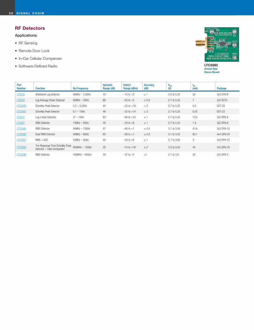
S I G N A L C H A I N5 0
RF Detectors
Applications:
• RF Sensing
• Remote Door Lock
• In-Car Cellular Compenser
• Software-Defined Radio
Part Number Function Op Frequency
Dynamic Range (dB)
Detect Range (dBm)
Accuracy (dB)
Vcc (V)
Icc (mA) Package
LT5538 Wideband Log Detector 40MHz – 3.8GHz 75 –75 to +5 ± 1 3.0 to 5.25 29 3x3 DFN-8
LT5534 Log Average Power Detector 50MHz – 3GHz 60 –63 to –2 ± 0.5 2.7 to 5.25 7 2x2 SC70
LTC5505 Schottky Peak Detector 0.3 – 3.5GHz 44 –32 to +18 ± 2 2.7 to 5.25 0.5 SOT-23
LTC5507 Schottky Peak Detector 0.1 – 1GHz 46 –32 to +14 ± 2 2.7 to 5.25 0.55 SOT-23
LT5537 Log-Linear Detector LF – 1GHz 83 –80 to +10 ± 1 2.7 to 5.25 13.5 3x2 DFN-8
LT5581 RMS Detector 10MHz – 6GHz 40 –34 to +6 ± 1 2.7 to 5.25 1.4 3x2 DFN-8
LTC5582 RMS Detector 40MHz – 10GHz 57 –56 to +1 ± 0.5 3.1 to 3.50 41.6 3x3 DFN-10
LTC5583 Dual RMS Detector 40MHz – 6GHz 60 –58 to +1 ± 0.2 3.1 to 3.50 90.1 4x4 QFN-24
LTC5587 RMS + ADC 10MHz – 6GHz 40 –34 to +6 ± 1 2.7 to 3.60 3 3x3 DFN-12
LTC55647ns Response Time Schottky Peak Detector + Fast Comparator
600MHz – 15GHz 25 –10 to +16 ± 2 3.0 to 5.50 44 3x3 QFN-16
LTC5596 RMS Detector 100MHz – 40GHz 35 –37 to –2 ±1 2.7 to 3.6 30 2x2 DFN-3
LTC5582 Actual Size Demo Board
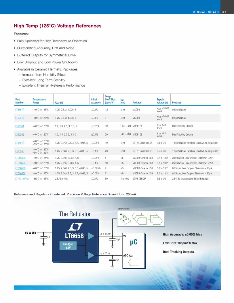
5 1S I G N A L C H A I N
Reference and Regulator Combined: Precision Voltage Reference Drives Up to 200mA
High Temp (125°C) Voltage References
Features:
• Fully Specified for High Temperature Operation
• Outstanding Accuracy, Drift and Noise
• Buffered Outputs for Symmetrical Drive
• Low Dropout and Low Power Shutdown
• Available in Ceramic Hermetic Packages
– Immune from Humidity Effect
– Excellent Long Term Stability
– Excellent Thermal Hysteresis Performance
Part Number
Temperature Range VOUT (V)
Initial Accuracy
Temp Coeff Max (ppm/°C)
IOUT (mA) Package
Supply Voltage (V) Features
LT6657A –40°C to 125°C 1.25, 2.5, 3, 4.096, 5 ±0.1% 1.5 ±10 MSOP8VOUT +50mV to 40
0.5ppm Noise
LT6657B –40°C to 125°C 1.25, 2.5, 3, 4.096, 5 ±0.1% 3 ±10 MSOP8VOUT +50mV to 40
0.5ppm Noise
LT6658A –40°C to 125°C 1.2, 1.8, 2.5, 3, 3.3, 5 ±0.05% 10 -40, +200 MSOP16EVOUT +2.5 to 36
Dual Tracking Outputs
LT6658B –40°C to 125°C 1.2, 1.8, 2.5 3, 3.3, 5 ±0.1% 20 -40, +200 MSOP16EVOUT +2.5 to 36
Dual Tracking Outputs
LT6654A–40°C to 125°C, –55°C to 125°C
1.25, 2.048, 2.5, 3, 3.3, 4.096, 5 ±0.05% 10 ±10 SOT23 Ceramic LS8 2.5 to 36 1.5ppm Noise, Excellent Load & Line Regulation
LT6654B–40°C to 125°C, –55°C to 125°C
1.25, 2.048, 2.5, 3, 3.3, 4.096, 5 ±0.1% 20 ±10 SOT23 Ceramic LS8 2.5 to 36 1.5ppm Noise, Excellent Load & Line Regulation
LTC6652A –40°C to 125°C 1.25, 2, 2.5, 3, 3.3, 4, 5 ±0.05% 5 ±5 MSOP8 Ceramic LS8 2.7 to 13.2 2ppm Noise, Low Dropout Shutdown <2µA
LTC6652B –40°C to 125°C 1.25, 2, 2.5, 3, 3.3, 4, 5 ±0.1% 10 ±5 MSOP8 Ceramic LS8 2.7 to 13.2 2ppm Noise, Low Dropout Shutdown <2µA
LTC6655B –40°C to 125°C 1.25, 2.048, 2.5, 3, 3.3, 4.096, 5 ±0.025% 2 ±5 MSOP8 Ceramic LS8 3.0 to 13.2 0.25ppm, Low Dropout Shutdown <20µA
LTC6655C –40°C to 125°C 1.25, 2.048, 2.5, 3, 3.3, 4.096, 5 ±0.05% 5 ±5 MSOP8 Ceramic LS8 3.0 to 13.2 0.25ppm, Low Dropout Shutdown <20µA
LT1431MP/M –55°C to 125°C 2.5, 5 or Adj. ±0.4% 50 1 to 100 SOP8 CERDIP 2.5 to 36 2.5V, 5V or Adjustable Shunt Regulator
LT66585V to 36V
Bandgap2.5V
V+10µF
Up to 150mA
Up to 50mA
1µF
1µF
Other Circuits
ADC VREF
µC
The Refulator +– +
– +–
High Accuracy: ±0.05% Max
Low Drift: 10ppm/˚C Max
Dual Tracking Outputs

Notes:

, LT, LTC, LTM, Linear Technology, the Linear logo, the Dust Networks logo, Burst Mode, Dust Networks, Over-The-Top, LTPoE++, LTpowerPlanner, LTpowerPlay, PolyPhase, Silent Switcher, SmartMesh, TimerBlox, and µModule are registered trademarks and Bat-Track, Easy Drive, isoSPI, PowerPath, SmartMesh IP, True Color PWM, and ThinSOT are trademarks of Analog Devices, Inc. All other trademarks are the property of their respective owners.
© 2017 Analog Devices, Inc.
Sales Of f icesNORTH AMERICA
WESTERN U.S.
2085 E . Technology Cir ., Ste . 101Tempe, AZ 85284Tel: (480) 777-1600Fax: (480) 838-1104
7595 Irvine Center Dr ., Ste . 120Irvine, CA 92618Tel: (949) 453-4650Fax: (949) 453-4765
11300 W . Olympic Blvd ., Ste . 700Los Angeles, CA 90064Tel: (818) 703-0835Fax: (818) 703-0517
720 Sycamore Dr .Milpitas, CA 95035Tel: (408) 428-2050Fax: (408) 432-6331
3009 Douglas Blvd ., Ste . 140Roseville, CA 95661Tel: (916) 787-5210Fax: (916) 787-0110
5465 Morehouse Dr ., Ste . 155San Diego, CA 92121Tel: (858) 638-7131Fax: (858) 638-7231
7102 La Vista Place, Ste . 201Niwot, CO 80503Tel: (303) 926-0002Fax: (303) 530-1477
Salt Lake City, NVTel: (801) 731-8008
5285 SW Meadows Rd ., Ste . 240Lake Oswego, OR 97035Tel: (503) 431-6960Fax: (503) 431-6961
2018 156th Ave . NE, Ste . 100Bellevue, WA 98007Tel: (425) 748-5010Fax: (425) 748-5009
MIDWEST U.S.
2040 E . Algonquin Rd ., Ste . 512Schaumburg, IL 60173Tel: (847) 925-0860
IndianaTel: (847) 925-0860
IowaTel: (847) 925-0860
KansasTel: (913) 634-7966
MichiganTel: (440) 239-0817
7805 Telegraph Rd ., Ste . 225Bloomington, MN 55438Tel: (952) 903-0605
MissouriTel: (913) 634-7966
Columbus, OHTel: (614) 488-4466
7550 Lucerne Dr ., Ste . 106Middleburg Heights, OH 44130Tel: (440) 239-0817Fax: (440) 239-1466
WisconsinTel: (262) 331-4040
NORTHEAST U.S.
ConnecticutTel: (860) 228-4104
15 Research PlaceNorth Chelmsford, MA 01863Tel: (978) 656-4750Fax: (978) 656-4760
New YorkTel: (978) 656-4750
3220 Tillman Dr ., Ste . 120Bensalem, PA 19020Tel: (215) 638-9667Fax: (215) 638-9764
SOUTHEAST U.S.
Huntsville, ALTel: (256) 881-9850
Fort Lauderdale, FLTel: (407) 688-7616
Orlando, FLTel: (407) 688-7616
Tampa, FLTel: (813) 634-9434
Atlanta, GATel: (770) 888-8137
170 Weston Oaks Ct .Cary, NC 27513Tel: (919) 677-0066Fax: (919) 678-0041
8500 N . Mopac, Ste . 603Austin, TX 78759Tel: (512) 795-8000Fax: (512) 795-0491
22515 Sail Harbour Ct .Katy, TX 77450Tel: (713) 463-5002
2301 W . Plano Pkwy ., Ste . 109Plano, TX 75075Tel: (972) 733-3071Fax: (972) 380-5138
CANADA
Calgary, ABTel: (403) 455-3577
Vancouver, BCTel: (604) 783-3084
Ottawa, ONTel: (613) 680-3473
Toronto, ONTel: (440) 239-0817
Montreal, QCTel: (514) 236-6261
ASIA/PACIFIC
AUSTRALIA/NEW ZEALAND
133 Alexander Street Crows Nest, NSW 2065, Australia Tel: +61 (0)2 9432 7803 Fax: +61 (0)2 9439 2738
Suite 121A, 89 High Street Kew, Victoria 3101, Australia Tel: +61 3 9854 6120
CHINA
Room 1763, Office Building New Century Hotel No . 6 Southern Road of Capital Gym Haidian District Beijing, China 100044 Tel: +86 (10) 6801-1080 Fax: +86 (10) 6805-4030
Unit 09, 14/F, Complex Building No . 88 Shenghe Yi Rd ., Hi-Tech Zone Sichuan Province, Chengdu City China 610041 Tel: +86 028-8555 9725 Fax: +86 028-8542 6859
Unit 1503-04, Metroplaza Tower 2 223 Hing Fong Road Kwai Fong, N .T ., Hong Kong Tel: +852 2428-0303 Fax: +852 2348-0885
Room 2701, City Gateway No . 398 Cao Xi North Road Shanghai, China 200030 Tel: +86 (21) 6375-9478 Fax: +86 (21) 5465-5918
Room 2109-2111, 21/F, Block D Southern International Plaza 3013 Yitian Road, Futian District Shenzhen, China 518048 Tel: +86 755-2360-4866 Fax: +86 755-2360-4966
Room 1805, Tower A Optics Valley International Plaza No . 889 Luoyu Rd ., Wuchang District Wuhan, China 430074 Tel: +86 027-8665 9231 Fax: +86 027-8665 9241
Rm . 2410, Tower A, Greenland SOHO No . 5 ZhangBa 1 Road High-Tech Development Zone Shaanxi Province Xian, China 710065 Tel: +86 029-6851 8978 /68518979 Fax: +86 029-6851 8976
INDIA
602, 6th Floor, Prestige Meridian-1 No . 29, MG Road, Bangalore 560001, India Tel: +91 80 4012-4610 Fax: +91 80 4012-4612
JAPAN
7F, Sakuradori Ohtsu KT Bldg . 3-20-22 Marunouchi, Naka-ku Nagoya-shi, 460-0002, Japan Tel: +81 (52) 955-0056 Fax: +81 (52) 955-0058
6F Kearny Place Honmachi Bldg . 1-6-13 Awaza, Nishi-ku Osaka-shi, 550-0011, Japan Tel: +81 (6) 6533-5880 Fax: +81 (6) 6543-2588
8F Shuwa Kioicho Park Bldg . 3-6 Kioicho Chiyoda-ku Tokyo, 102-0094, Japan Tel: +81 (3) 5226-7291 Fax: +81 (3) 5226-0268
KOREA
10F, Yundang Building 439 Teheran-Ro, Gangnam-Gu Seoul, Korea 06158 Tel: +82 (2) 792-1617 Fax: +82 (2) 792-1619
SINGAPORE
507 Yishun Industrial Park A Singapore 768734 Tel: +65 6753-2692 Fax: +65 6752-0108
TAIWAN
8F-1, 77, Nanking E . Rd ., Sec . 3 Taipei, Taiwan Tel: +886 (2) 2505-2622 Fax: +886 (2) 2516-0702
EUROPE
FINLAND
Kirkkokatu 31 90100 Oulu, Finland Tel: +358 (0)46 712 2171 Fax: +358 (0)46 712 2175
Teknobulevardi 3-5, P .O . Box 35 FIN-01531 Vantaa, Finland Tel: +358 (0)46 712 2171 Fax: +358 (0)46 712 2175
FRANCE
Parc Tertiaire Silic 2 Rue de la Couture, BP10217 94518 Rungis CEDEX, France Tel: +33 (1) 56 70 19 90 Fax: +33 (1) 56 70 19 94
GERMANY
Haselburger Damm 4 D-59387 Ascheberg, Germany Tel: +49 (2593) 9516-0 Fax: +49 (2593) 951679
Osterfeldstrasse 84, Haus C D-85737 Ismaning, Germany Tel: +49 (89) 962455-0 Fax: +49 (89) 963147
Jesinger Strasse 65 D-73230 Kirchheim/Teck, Germany Tel: +49 (0)7021 80770 Fax: +49 (0)7021 807720
ITALY
Via Torri Bianche 3, Palazzo Larice 20871 Vimercate (MB), Italy Tel: +39 039 596 5080 Fax: +39 039 596 5090
SWEDEN
Electrum 204, Isafjordsgatan 22 SE-164 40 Kista, Sweden Tel: +46 (8) 623 16 00 Fax: +46 (8) 623 16 50
UNITED KINGDOM
3 The Listons, Liston Road Marlow, Buckinghamshire SL7 1FD United Kingdom Tel: +44 (1628) 477066 Fax: +44 (1628) 478153

1630 McCarthy Blvd . Milpitas, CA 95035-7417 • Tel: 408-432-1900 • www.linear.com CF101610KU
25%


