Automotive Three Phase MOSFET Driver A4939
20
Description The A4939 is a three-phase controller for use with N-channel external power MOSFETs and is specifically designed for automotive applications. A unique charge pump regulator provides full (>10 V) gate drive at battery voltages down to 7 V and allows the A4939 to operate with reduced gate drive at battery voltages down to 5.5 V. A bootstrap capacitor is used to provide the above battery supply voltage required for N-channel MOSFETs. One logic level input is provided for each of the six power MOSFETs in the 3-phase bridge, allowing motors to be driven with any commutation scheme defined by an external controller. The power MOSFETs are protected from cross-conduction by integrated crossover control. Motor phase short-to-supply and short-to-ground detection is provided by independent drain-source voltage monitors on each MOSFET. Short faults, supply undervoltage, and chip overtemperature conditions are indicated by a single open drain fault output. Product variants incorporating a low drop out (LDO) regulator to source either 5.0 V or 3.3 V to external circuitry are available. The A4939 is supplied in a 28-pin TSSOP power package with an exposed thermal pad (package type LP). This package is lead (Pb) free, with 100% matte-tin leadframe plating (suffix T). A4939-DS, Rev. 1 Features and Benefits • High current 3-phase gate drive for N-channel MOSFETs • Cross-conduction protection • 5.5 to 50 V supply voltage range • Regulated logic supply voltage output option • Motor phase short to supply and short to ground detection • Undervoltage, overtemperature monitors • Low current Sleep mode option Applications • Electronic power steering (EPS, EHPS, EAS) • Hydraulic pumps • Engine cooling fan • Gearbox actuator Automotive Three Phase MOSFET Driver Package: 28-pin TSSOP with exposed thermal pad (suffix LP) Typical Application Diagram Not to scale A4939 3-Phase BLDC Motor A4939 VBAT VDD Micro- controller
-
Upload
phamkhuong -
Category
Documents
-
view
237 -
download
0
Transcript of Automotive Three Phase MOSFET Driver A4939

DescriptionThe A4939 is a three-phase controller for use with N-channel external power MOSFETs and is specifically designed for automotive applications.
A unique charge pump regulator provides full (>10 V) gate drive at battery voltages down to 7 V and allows the A4939 to operate with reduced gate drive at battery voltages down to 5.5 V. A bootstrap capacitor is used to provide the above battery supply voltage required for N-channel MOSFETs.
One logic level input is provided for each of the six power MOSFETs in the 3-phase bridge, allowing motors to be driven with any commutation scheme defined by an external controller. The power MOSFETs are protected from cross-conduction by integrated crossover control.
Motor phase short-to-supply and short-to-ground detection is provided by independent drain-source voltage monitors on each MOSFET. Short faults, supply undervoltage, and chip overtemperature conditions are indicated by a single open drain fault output.
Product variants incorporating a low drop out (LDO) regulator to source either 5.0 V or 3.3 V to external circuitry are available. The A4939 is supplied in a 28-pin TSSOP power package with an exposed thermal pad (package type LP). This package is lead (Pb) free, with 100% matte-tin leadframe plating (suffix T).
A4939-DS, Rev. 1
Features and Benefits• High current 3-phase gate drive for N-channel MOSFETs• Cross-conduction protection• 5.5 to 50 V supply voltage range• Regulated logic supply voltage output option• Motor phase short to supply and short to ground detection• Undervoltage, overtemperature monitors• Low current Sleep mode option
Applications• Electronic power steering (EPS, EHPS, EAS)• Hydraulic pumps• Engine cooling fan• Gearbox actuator
Automotive Three Phase MOSFET Driver
Package: 28-pin TSSOP with exposed thermal pad (suffix LP)
Typical Application Diagram
Not to scale
A4939
3-Phase BLDC Motor
A4939
VBAT
VDD
Micro-controller
Automotive Three Phase MOSFET DriverA4939
2Allegro MicroSystems, LLC115 Northeast CutoffWorcester, Massachusetts 01615-0036 U.S.A.1.508.853.5000; www.allegromicro.com
Absolute Maximum Ratings with respect to GNDCharacteristic Symbol Notes Rating Unit
Load Supply Voltage VBB –0.3 to 50 V
Logic Monitor or Supply VDDM, V3, V5VDDM if no internal LDO regulator, V3 or V5 if LDO regulator present –0.3 to 7 V
Terminal VREG –0.3 to 16 V
Terminals CP1, CP2 –0.3 to 16 V
Logic Inputs AHI, ALO, BHI, BLO, CHI, CLO –0.3 to 6.5 V
Terminal VBRG –5 to 55 V
Terminal LSS –4 to 6.5 V
Terminals SA, SB, SC –5 to 55 V
Terminals GHA, GHB, GHC Sx to Sx+15 V
Terminals GLA, GLB, GLC –5 to 16 V
Terminals CA, CB, CC –0.3 to Sx + 15 V
Terminal FAULT –0.3 to 6.5 V
Terminal VDSTH –0.3 to 6.5 V
Ambient Operating Temperature Range TA Limited by power dissipation –40 to 150 °C
Maximum Continuous Junction Temperature TJ(max) 165 °C
Transient Junction Temperature TtJ
Over temperature event not exceeding 10s, lifetime duration not exceeding 10hours, determined by design characterisation.
175 °C
Storage Temperature Range Tstg –55 to 150 °C
Thermal Characteristics may require derating at maximum conditions, see application informationCharacteristic Symbol Test Conditions* Value Unit
Package Thermal Resistance (Junction to Ambient) RθJA
On 4-layer PCB based on JEDEC standard 28 ºC/W
On 2-layer PCB with 3.8 in2 copper each side 32 ºC/W
Package Thermal Resistance (Junction to Pad) RθJP 2 ºC/W
*Additional thermal information available on the Allegro website.
Selection GuidePart Number Sleep Mode Regulator Packing Package
A4939KLPTR-T Yes –
4000 pieces per 13-in. reel 9.7 mm × 4.4 mm, 1.2 mm nominal height28-pin TSSOP with exposed thermal padA4939KLPTR-3-T – 3.3 V
A4939KLPTR-5-T – 5 V

Automotive Three Phase MOSFET DriverA4939
3Allegro MicroSystems, LLC115 Northeast CutoffWorcester, Massachusetts 01615-0036 U.S.A.1.508.853.5000; www.allegromicro.com
Table of ContentsSpecifications 2
Absolute Maximum Ratings 2Thermal Characteristics 2Pin-out Diagram and Terminal Lists 4Functional Block Diagram 5Electrical Characteristics 6
Functional Description 9Input and Output Terminal Functions 9Power Supplies 10
CP1,CP2, VREG 10Sleep Mode 10Gate Drives 10
High-Side Gate Drives (GHA, GHB, GHC) 10Bootstrap Charge Management 10Low-side Gate Drive (GLA, GLB, GLC) 11
Drain Source Voltage Monitor 11Logic Control Inputs 12Diagnostics 12
Fault States 12Low Drop Out (LDO) Regulator 14
Applications Information 15Power Bridge Management Using PWM Control 15Bootstrap Capacitor Selection 15Bootstrap Charging 16VREG Capacitor Selection 16LDO Regulator Capacitor Selection 16Supply Decoupling 16Input/Output Structures 17Layout Recommendations 18Package Outline Drawing 19
Automotive Three Phase MOSFET DriverA4939
4Allegro MicroSystems, LLC115 Northeast CutoffWorcester, Massachusetts 01615-0036 U.S.A.1.508.853.5000; www.allegromicro.com
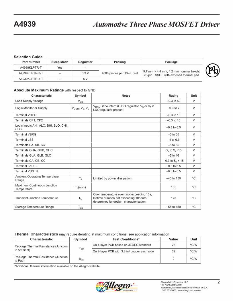
Pin-out Diagrams
A4939x-5 variant A4939x (No LDO) variantA4939x-3 variant
Name Number Function
LSS 1 Low-side Source
GLC 2 Low-side Gate Drive Phase C
GHC 3 High-side Gate Drive Phase C
SC 4 Motor Connection Phase C
CC 5 Bootstrap Capacitor Phase C
GLB 6 Low-side Gate Drive Phase B
GHB 7 High-side Gate Drive Phase B
SB 8 Motor Connection Phase B
CB 9 Bootstrap Capacitor Phase B
GLA 10 Low-side Gate Drive Phase A
GHA 11 High-side Gate Drive Phase A
SA 12 Motor Connection Phase A
CA 13 Bootstrap Capacitor Phase A
VREG 14 Gate Drive Supply Output
CP2 15 Pump Capacitor
LSS
GLC
GHC
SC
CC
GLB
GHB
SB
CB
GLA
GHA
SA
CA
VREG
CLO
CHI
BLO
BHI
ALO
AHI
FAULT
VDSTH
V5
GND
VBRG
VBB
CP1
CP2
1
2
3
4
5
6
7
8
9
10
11
12
13
14
28
27
26
25
24
23
22
21
20
19
18
17
16
15
PAD
LSS
GLC
GHC
SC
CC
GLB
GHB
SB
CB
GLA
GHA
SA
CA
VREG
CLO
CHI
BLO
BHI
ALO
AHI
FAULT
VDSTH
V3
GND
VBRG
VBB
CP1
CP2
1
2
3
4
5
6
7
8
9
10
11
12
13
14
28
27
26
25
24
23
22
21
20
19
18
17
16
15
PAD
LSS
GLC
GHC
SC
CC
GLB
GHB
SB
CB
GLA
GHA
SA
CA
VREG
CLO
CHI
BLO
BHI
ALO
AHI
FAULT
VDSTH
VDDM
GND
VBRG
VBB
CP1
CP2
1
2
3
4
5
6
7
8
9
10
11
12
13
14
28
27
26
25
24
23
22
21
20
19
18
17
16
15
PAD
Terminal List TableName Number Function
CP1 16 Pump Capacitor
VBB 17 Main Power Supply
VBRG 18 High-side bridge voltage sense
GND 19 Ground
V3V5
VDDM 20
Voltage Supply (Output) – A4939x-3Voltage Supply (Output) – A4939x-5Monitor Input – A4939x (No LDO)
VDSTH 21 VDS Monitor Threshold Voltage
FAULT 22 Programmable diagnostic output
AHI 23 Phase A high-side control input
ALO 24 Phase A low-side control input
BHI 25 Phase B high-side control input
BLO 26 Phase B low-side control input
CHI 27 Phase C high-side control input
CLO 28 Phase C low-side control input
Pad – Exposed thermal pad on underside

Automotive Three Phase MOSFET DriverA4939
5Allegro MicroSystems, LLC115 Northeast CutoffWorcester, Massachusetts 01615-0036 U.S.A.1.508.853.5000; www.allegromicro.com
ChargePump
RegulatorLDO
Regulator
Logic SupplyRegulator
VBAT
CP2CP1
LSS
GLA
GHA
SA
CA
VREG
Battery +
VREG
Phase A
VBB
Phase C
Phase B
CBOOTA
CREG
CP
VBRG
VDSMonitor
VDSMonitor
GND
FAULT
VDSTH
V3 (A4939x-3)V5 (A4939x-5)VDDM (A4939x)
ControlLogic
Diagnosticsand
Protection
One of three phases shown
RGATE
RGATE
High Side Drive
Low Side Drive
(A4939x-3)(A4939x-5)
AHI
ALO
BHI
BLO
CHI
CLO
A
A External pin acts as a monitor input (VDDM) on variants without LDO regulator, and a supply voltage output on variants with LDO regulator (designated V3 or V5 for 3.3 V and 5.0 V variants respectively)
Automotive Three Phase MOSFET DriverA4939
6Allegro MicroSystems, LLC115 Northeast CutoffWorcester, Massachusetts 01615-0036 U.S.A.1.508.853.5000; www.allegromicro.com
ELECTRICAL CHARACTERISTICS1 Valid at TJ = –40°C to 150°C, VBB = 7 to 50 V; unless otherwise specifiedCharacteristic Symbol Test Conditions Min. Typ. Max. Unit
Supply and ReferenceVBB Functional Operating Range2 VBB Correct function, parameters not guaranteed 5.5 – 50 V
VBB Quiescent Current3IBBQ Operational mode, outputs low, VBB = 12 V – 10 14 mA
IBBSSleep mode, VBB = 12 V (A4939x, No LDO, variant) – – 15 µA
VREG Output Voltage VREG
VBB > 9 V, IREG = 0 to 15 mA 12.5 13 13.75 V
7.5 V < VBB ≤ 9 V, IREG = 0 to 10 mA 12 13 13.75 V
6 V < VBB ≤ 7.5 V, IREG = 0 to 9 mA 2×VBB – 3.0 – – V
5.5 V < VBB ≤ 6 V, IREG < 8 mA 8.5 9.5 – V
Bootstrap Diode Forward Voltage VfBOOTID = 10 mA 0.4 0.7 1.0 V
ID = 100 mA 1.5 2.2 3.1 V
Bootstrap Diode Resistance rDrD(100mA) = (VfBOOT(150mA) – VfBOOT(50mA)) / 100 (mA) 6 13 28 Ω
Bootstrap Diode Current Limit IDBOOT 250 500 750 mA
Gate Output DriveTurn-On Time tr CLOAD = 1nF, 20% to 80% – 35 – ns
Turn-Off Time tf CLOAD = 1nF, 80% to 20% – 20 – ns
Pull-Up On Resistance RDS(on)UPTJ = 25°C, IGHx = –150 mA 5 8 13 Ω
TJ = 150°C, IGHx = –150 mA 10 15 24 Ω
Pull-Down On Resistance RDS(on)DNTJ = 25°C, IGLx = 150 mA 1.5 2.4 4.6 Ω
TJ = 150°C, IGLx = 150 mA 2.5 4 6.5 Ω
GHx Output Voltage – High VGHH Bootstrap capacitor fully charged VCx – 0.2 – – V
GHx Output Voltage – Low VGHL – – VSX + 0.3 V
GLx Output Voltage – High VGLH VREG – 0.2 – – V
GLx Output Voltage – Low VGLL – – VLSS + 0.3 V
GHx Passive Pull-Down Resistance RGHPD VGHx – VSx < 0.3 V – 400 – kΩ
GLx Passive Pull-Down Resistance RGLPD VGLx – VLSS < 0.3 V – 400 – kΩ
Turn-Off Propagation Delay4 tP(off) Input change to unloaded gate output change 60 90 180 ns
Turn-On Propagation Delay4 tP(on) Input change to unloaded gate output change 60 90 180 ns
Propagation Delay Matching – Phase to Phase ∆tPP Same phase change – 10 – ns
Propagation Delay Matching – On to Off ∆tOO Single phase – 30 – ns
Continued on the next page…

Automotive Three Phase MOSFET DriverA4939
7Allegro MicroSystems, LLC115 Northeast CutoffWorcester, Massachusetts 01615-0036 U.S.A.1.508.853.5000; www.allegromicro.com
ELECTRICAL CHARACTERISTICS1 (continued) Valid at TJ = –40°C to 150°C, VBB = 7 to 50 V; unless otherwise specifiedCharacteristic Symbol Test Conditions Min. Typ. Max. Unit
Logic Inputs and OutputsInput Low Voltage VIL – – 0.8 V
Input High Voltage VIH 2.0 – – V
Input Hysteresis VIhys 100 300 – mV
Input Pull-Down Resistor (xHI, xLO) RPD – 50 – kΩ
Input Pulse Filter Time (xHI, xLO) tPIN – 35 – ns
VDS Disable Voltage VDSD – – 100 mV
Fault Disable Voltage VFLTD – – 0.5 V
Output Low Voltage (FAULT) VOL IOL = 1 mA, no fault indicated – 0.2 0.4 V
Output Leakage (FAULT)5 IO 0 V < VO < 5.5 V, fault indicated –1 – 1 µA
Protection
VREG Undervoltage LockoutVREGON VREG rising 7.5 8 8.5 V
VREGOFF VREG falling 6.75 7.25 7.75 V
Bootstrap Undervoltage Threshold VBOOTUV VBOOT falling, VCx – VSx 62 – 75 %VREG
Bootstrap Undervoltage Hysteresis VBOOTHys – 9 – %VREG
VDDM / V3 / V5 Undervoltage Threshold6 VDDUV Voltage falling 2.45 2.7 2.85 V
VDDM / V3 / V5 Undervoltage Hysteresis6 VDDUVHys 40 100 160 mV
VDS Threshold – Internal VDSTHI VDSTH > 2.7 V 1.1 1.2 1.3 V
VDS Threshold Range VDSTH 0.2 – 2 V
VDS Threshold Input Leakage VDSTHL 0 V < VDSTH < 5.5 V – 3 – 3 µA
VBRG Input Voltage VBRG VBB – 1 VBB VBB + 1 V
VBRG Input Current IVBRG VDSTH = 2 V, VBB = 12 V, 0 V < VBRG < VBB – – 250 µA
Short-to-Ground Threshold Offset VSTGOVDSTH ≥ 1 V – ±100 – mV
VDSTH < 1 V –150 ±50 +150 mV
Short-to-Battery threshold offset VSTBOVDSTH ≥ 1 V – ±100 – mV
VDSTH < 1 V –150 ±50 +150 mV
VDS Fault Blank Time tBL 1.5 2.3 4.5 µs
Overtemperature Warning TJF Temperature increasing 170 – 180 ºC
Overtemperature Hysteresis TJHyst Recovery = TJF – TJHyst – 15 – ºC
Variant without LDO Regulator Only (A4939x)Sleep Mode Activation Timeout (xHI, xLO)3 tSLT From all xHI, xLO < VIL 7.5 10 12.5 ms
Wake-up from Sleep Delay3 tWK Any xHI, xLO > VIH , CREG < 1 µF – – 1 ms
VDDM Pull-Down Resistor RVDDM – 60 – kΩ
Continued on the next page…

Automotive Three Phase MOSFET DriverA4939
8Allegro MicroSystems, LLC115 Northeast CutoffWorcester, Massachusetts 01615-0036 U.S.A.1.508.853.5000; www.allegromicro.com
ELECTRICAL CHARACTERISTICS1 (continued) Valid at TJ = –40°C to 150°C, VBB = 7 to 50 V; unless otherwise specifiedCharacteristic Symbol Test Conditions Min. Typ. Max. Unit
5 V LDO Regulator Variant Only (A4939x-5 )7
V5 Output Voltage V5IV5 < 70 mA, VBB > 6 V 4.85 – 5.25 V
5 mA < IV5 < 25 mA 4.9 5.0 5.2 V
V5 Output Overcurrent Limit ILDOOC(V5) 130 – 260 mA
V5 Shutdown Voltage Threshold VLDOSD(V5) Voltage falling 450 – 850 mV
V5 Shutdown Voltage Hysteresis VLDOHys(V5) 80 – 200 mV
V5 Pilot Current8 ILDOP(V5) LDO regulator shut down – 2 – mA
V5 Shutdown Lockout Period tLDOL(V5) From V5 < VLDOSD(V5) – 2 – ms
3 V LDO Regulator Variant Only (A4939x-3 )7
V3 Output Voltage V3IV3 < 70 mA, VBB > 6 V 3.15 – 3.53 V
5 mA < IV3 < 25 mA 3.2 3.3 3.5 V
V3 Output Overcurrent Limit ILDOOC(V3) 130 – 260 mA
V3 Shutdown Voltage Threshold VLDOSD(V3) Voltage falling 450 – 850 mV
V3 Shutdown Voltage Hysteresis VLDOHys(V3) 80 – 200 mV
V3 Pilot Current8 ILDOP(V3) LDO regulator shut down – 2 – mA
V3 Shutdown Lockout Period tLDOL(V3) From V3 < VLDOSD(V3) – 2 – ms1Specifications presented apply to all product variants except where variant-specific limitations are explicitly defined.2Function is correct but parameters are not guaranteed below the general limits (7 V).3Sleep mode entered after logic low (less than VIL) simultaneously detected on all xLO and xHI inputs for a period of tSLT . Operating mode resumed within tWK of logic high (greater than VIL ) being detected on any of the xLO or xHI pins.4See figure 1 for gate drive output timing.5For input and output current specifications, negative current is defined as coming out of (sourced by) the specified device terminal.6On product variants with LDO regulator (A4939x-3 and A4939x-5), an undervoltage trip sets all gate drive outputs low and an unlatched fault state on the FAULT pin. On product variants without LDO regulator (A4939x), an undervoltage trip has no effect on device operation but sets an unlatched fault state on the FAULT pin.7A capacitance of at least 1 µF with an ESR of no more than 250 mΩ should be fitted between the LDO V3 / V5 output and GND to ensure stability.8Pilot current is disabled while the overtemperature warning is active.
Figure 1: Gate Drive Timing
GHx
GLx
tP(off)
xHI
xLO
tP(on) tP(off) tP(on)

Automotive Three Phase MOSFET DriverA4939
9Allegro MicroSystems, LLC115 Northeast CutoffWorcester, Massachusetts 01615-0036 U.S.A.1.508.853.5000; www.allegromicro.com
Functional Description
The A4939 provides six high current gate drives capable of driv-ing a wide range of N-channel power MOSFETs. The gate drives are configured as three high-side drives and three low-side. The six gate drives are controlled by individual TTL-threshold logic inputs which may be driven from 3.3 V or 5 V logic outputs.
The A4939 provides all necessary circuitry to ensure that the gate-source turn-on voltages of both high-side and low-side external MOSFETs are driven above 10 V at supply voltages down to 7 V. For extreme low battery voltage conditions, cor-rect functional operation is maintained down to 5.5 V but with a reduced gate drive.
The control inputs to the A4939 provide a simple solution for many motor drive applications controlled by an external micro-controller or DSP. Phase commutation and PWM control must be managed by the external system controller.
Specific device functions are described more fully in the follow-ing sections.
Input and Output Terminal FunctionsVBB Power supply for all device functions including internal logic and charge pump. Also used to power the LDO regulator where present.
System power should be connected to VBB through a reverse voltage protection circuit. The VBB pin should be decoupled to ground with ceramic capacitors mounted physically close to the device pins.
VDDM Unique to A4939x variant (has no LDO regulator). May be considered an undervoltage fault monitor input. It is not neces-sary to apply a voltage on this pin to power the A4939 and it is not possible to draw power from it to support external circuitry. If the voltage on VDDM drops below the VDDUV undervoltage threshold an unlatched fault condition is set on the FAULT pin. If it rises above VDDUV + VDDUVHys the fault condition is cleared. Because a pull-down resistance (60 kΩ typical) is connected from VDDM to ground within the A4939 device, it is recommended that the pin be connected directly (or pulled-up via a suitable resistor) to the external system logic supply or similar, to avoid unwanted fault states being set on the FAULT output.
V3 Unique to A4939x-3 variant (has a 3.3 V LDO regulator). Sources 3.3 V to power external circuitry but does not power any on-chip functions. Must be loaded with appropriate capacitance as detailed in the Electrical Characteristics table.
V5 Unique to A4939x-5 variant (has a 5 V LDO regulator). Sources 5 V to power external circuitry but does not power any on-chip functions. Must be loaded with appropriate capacitance as detailed in the Electrical Characteristics table.
CP1, CP2 Pump capacitor connection for charge pump. Connect a minimum 220 nF capacitor, typically 470 nF, between CP1 and CP2.
VREG Regulated voltage, nominally 13 V, used to supply the low-side gate drivers and to charge the bootstrap capacitors. A sufficiently large storage capacitor must be connected to this terminal to provide the transient charging current.
GND Analog reference, digital, and power ground. Connect to supply ground (see Layout Recommendations section).
CA, CB, CC High-side connections for the bootstrap capacitors and positive supply for high-side gate drivers.
GHA, GHB, GHC High-side, gate-drive outputs for external N-channel MOSFETs.
SA, SB, SC Motor phase connections. Used to sense the voltages switched across the load. Also connected to the negative side of the bootstrap capacitors and constitute the negative supply con-nections for the floating high-side drivers.
GLA, GLB, GLC Low-side, gate-drive outputs for external N-channel MOSFETs.
LSS Low-side return path for discharge of the capacitance on the MOSFET gates, connected to the common sources of the low-side external MOSFETs through a low impedance PCB trace.
VBRG Sense input to the top of the external MOSFET bridge. Allows accurate measurement of the voltage at the drains of the high side MOSFETs.
AHI, BHI, CHI Input to control the high-side gate drives. A logic high on the pin commands the relevant high-side gate drive to be activated.

Automotive Three Phase MOSFET DriverA4939
10Allegro MicroSystems, LLC115 Northeast CutoffWorcester, Massachusetts 01615-0036 U.S.A.1.508.853.5000; www.allegromicro.com
ALO, BLO, CLO Input to control the low-side gate drives. A logic high on the pin commands the relevant low-side gate drive to be activated.
FAULT Open drain active-high fault output. If a fault is present the open-drain pull-down is off and the FAULT output may be pulled high by an external pull-up resistor connected to any volt-age up to a maximum of 5.5 V.
VDSTH Drain source fault threshold programming pin. The VDS fault threshold may be set by applying an externally generated analog voltage. VDS fault reporting is disabled if VDSTH is driven to less than VDSD (for example, shorted to ground). The VDS fault threshold is set to an internally hardwired value, VDSTHI, if VDSTH is driven to a voltage above its specified analog input range (for example, pulled-up to the system logic supply voltage).
Power SuppliesA single supply voltage applied to the VBB pin powers all device functions including on-chip logic, analog circuitry, output drivers and the LDO regulator (where present). The supply should be connected to VBB through a reverse voltage protection circuit and decoupled by way of a ceramic capacitor mounted close to the VBB and GND terminals. All variants of the A4939 will operate within specified performance limits with VBB between 7 and 50 V, and will function correctly with VBB as low as 5.5 V.
CP1,CP2, VREG The gate drivers are powered by an internal regulator which limits the supply to the drivers and therefore the maximum gate voltage. For VBB supply greater than approximately 16 V, the regulator is a simple buck regulator. Below 16 V, the regulated supply is maintained by a charge pump boost converter which requires a pump capacitor, typically 470 nF, connected between the CP1 and CP2 terminals. The regulated voltage, nominally 13 V, is available on the VREG terminal. A sufficiently large storage capacitor (see the Applications Information section) must be connected to this terminal to provide the transient charging current to the low-side drivers and the bootstrap capacitors.
Sleep ModeA low power Sleep mode is available on the A4939x (no LDO regulator) variant. It is activated after logic low is detected
simultaneously on all xLO and xHI inputs for a period equal to the Sleep Mode Activation Timeout (tSLT). In Sleep mode all outputs are switched to a high impedance state.
Operating mode is activated within a period equal to the Wake-up from Sleep Delay (tWK) from when a logic high is detected on any of the xLO or xHI pins. It is recommended that all xLO inputs be simultaneously driven to logic high (GLx turned on) when waking from Sleep mode, in order to recharge the bootstrap capacitors and enable subsequent high-side turn on.
Sleep mode is not available on A4939x-3 and A4939-5 (LDO regulator) variants. If all logic inputs are taken low, power consumption remains unchanged and all functions remain opera-tional.
Gate DrivesThe A4939 is designed to drive external, low on-resistance, power N-channel MOSFETs. It will supply the large transient currents necessary to quickly charge and discharge the exter-nal MOSFET gate capacitances in order to reduce dissipation in the external MOSFET during switching. Charge current for the low-side drives is provided directly by the capacitor on the VREG terminal. Charge current for the high-side drives is delivered via the bootstrap capacitors connected, one per phase, across the Cx – Sx terminal pairs. Charge and discharge rate can be controlled by incorporating an external resistor in series with each MOSFET gate drive (GHx, GLx).
High-Side Gate Drives (GHA, GHB, GHC) These are the high-side gate drive outputs for external N-channel MOSFETs. An external resistor between the GHx gate drive output and the MOSFET gate terminal (mounted as close to the latter as possible) may be used to control the slew rate at the gate, thereby controlling the di/dt and dv/dt at the Sx terminals. Setting GHx high turns-on the upper half of the driver, sourcing current to the gate of the high-side MOSFET in the external motor-driv-ing bridge, turning it on. Setting GHx low turns-on the lower half of the driver, sinking current from the external MOSFET gate circuit to the respective Sx terminal, turning it off.
Bootstrap Charge Management Bootstrap capacitors are charged to approximately VREG when the associated Sx terminal is driven low. When the Sx terminal subsequently goes high, the capacitor provides the necessary volt-

Automotive Three Phase MOSFET DriverA4939
11Allegro MicroSystems, LLC115 Northeast CutoffWorcester, Massachusetts 01615-0036 U.S.A.1.508.853.5000; www.allegromicro.com
age for high-side N-channel power MOSFET turn-on. At system start-up it is necessary to turn on each low-side drive (GLx) prior to attempting to turn on the complementary high-side (GHx), in order to charge the bootstrap capacitors.
Low-side Gate Drive (GLA, GLB, GLC)The low-side, gate-drive outputs on GLA, GLB, and GLC are referenced to the LSS terminal. These outputs are designed to drive external N-channel power MOSFETs. An external resistor between the GLx gate drive output and the MOSFET gate ter-minal (mounted as close to the latter as possible) may be used to control the slew rate at the gate, thereby providing some control of the di/dt and dv/dt at the Sx terminals. Setting GLx high turns-on the upper half of the driver, sourcing current to the gate of the low-side MOSFET in the external motor-driving bridge, turning it on. Setting GLx low turns-on the lower half of the driver, sink-ing current from the external MOSFET gate circuit to the to the LSS terminal, turning it off.
Drain Source Voltage MonitorThe VDS fault threshold is set by applying a control voltage on the VDSTH pin, as detailed in figure 2. If a voltage between 0.2 and 2.0 V is applied, the threshold follows this level, subject to the Short to Ground Threshold (VSTGO) and Short to Battery Threshold (VSTBO) offsets detailed in the Electrical Characteris-tics table.
If a voltage between 2.0 and 2.3 V is applied, the threshold approximates the applied level, but accuracy is not specified.
If the VDSTH pin is driven below the VDS Disable Voltage (VDSD), 0.1 V (such as when shorted to ground), VDS fault reporting is disabled.
If the VDSTH pin is taken above 2.7 V (such as when pulled up to the system logic supply voltage) the threshold is set to the VDS Threshold Internal voltage (VDSTH), detailed in the Electri-cal Characteristics table (typically 1.2 V).
The VDSTH pin presents a high impedance at all voltages across its permissible input range (per the VDS Threshold Input Leak-age limits, VDSTHL , detailed in the Electrical Characteristics table) allowing a wide range of programming circuits to be used including simple resistive dividers.
The VDSTH input has an internal passive first-order filter with a
1 VDSTH pin typically tied to system logic supply voltage (for example, V3 or V5)
2 Behaviour indeterminate due to threshold detection uncertainty 3 Threshold range confirmed by design
0 V
2.0 V
0.2 V
External
(Threshold set to voltage applied on VDSTH pin with accuracy specified in
Electrical Characteristics table)
0.1 V
2.3 V
2.7 V
5.5 V
Disabled
External
(Threshold set to voltage approximately equal to that applied on VDSTH pin. Accuracy not specified.)
Indeterminate2, 3
Indeterminate2
Internal1
(Threshold set to internal value, VDSTHI, with accuracy specified in Electrical
Characteristics table)
VDSD
VDSTH (min)
VDSTH (max)
Figure 2: VDSTH Pin Voltage versus VDS Monitor Function

Automotive Three Phase MOSFET DriverA4939
12Allegro MicroSystems, LLC115 Northeast CutoffWorcester, Massachusetts 01615-0036 U.S.A.1.508.853.5000; www.allegromicro.com
time constant of approximately 0.01 ms. Additional filter capaci-tance may be added externally if required.
Logic Control InputsA set of discrete digital inputs (xHI and xLO) provides direct control of the six gate drive outputs (GHx and GLx). TTL input threshold levels ensure these can be driven from 3.3 V or 5 V logic systems. Setting a logic input high causes the corresponding gate drive output to go high, thereby commanding the associated external MOSFET to turn on. Conversely, setting a logic input low causes the corresponding gate drive to go low, commanding the MOSFET to turn off.
Internal lock-out logic, detailed in table 1, ensures that the high-side output drive and low-side output drive cannot be active simultaneously.
Table 1: Phase Control Truth TableInput Output Phase
xHI xLO GHx GLx Sx Comment
0 0 L L Z Phase disabled
0 1 L H LO Low-side active
1 0 H L HI High-side active
1 1 L L Z Phase disabled
HI = high-side MOSFET active LO = low-side MOSFET active Z = high impedance, both MOSFETs off
DiagnosticsSeveral diagnostic features are integrated into the A4939 to indicate fault conditions. In addition to system-wide faults such as undervoltage and overtemperature, the A4939 integrates individual monitors for each bootstrap capacitor voltage and each external MOSFET drain-source voltage.
The presence of a fault condition is indicated on the FAULT pin. This is an open drain output that should be pulled to any voltage, up to 5.5 V, by an external resistor, typically 10 to 47 kΩ. The definition of the individual fault states and the effects on the gate drive outputs (GHx and GLx) are shown in table 2 and described below.
Fault StatesIt is recommended that any external control circuitry remaining active in the event of a fault state being flagged be configured to take appropriate action to prevent damage to the A4939 and associated motor drive components.
Overtemperature If the junction temperature exceeds the overtemperature warning threshold (TJF), the A4939 enters the overtemperature warning state and FAULT goes high. When the junction temperature drops below the recovery level ( TJF – TJF hys ), the overtemperature warning state is cleared and the FAULT output returned to logic low.
While an overtemperature warning state is being asserted, no on-chip circuitry or functions are disabled, with the exception of the LDO regulator on the A3939x-3 and A4939x-5 variants, which is
Table 2: Fault DefinitionsFAULT Pin
State Fault Description Outputs Disabled Fault Latched
Low No fault No –
High Overtemperature No No
High
VDDM undervoltage(A4939x variant, without LDO) Gate drives remain active
NoV3 or V5 undervoltage
(A4939x-3 and A4939x-5 variants, with LDO) All gate drives low (external MOSFETs off)
High VREG undervoltage All gate drives low (external MOSFETs off) No
High VDS overvoltage No No
High Bootstrap undervoltageHigh-side drive of the output phase that is generating the fault condition is set low (external MOSFET off). Other outputs unaffected.
Yes

Automotive Three Phase MOSFET DriverA4939
13Allegro MicroSystems, LLC115 Northeast CutoffWorcester, Massachusetts 01615-0036 U.S.A.1.508.853.5000; www.allegromicro.com
shut down immediately and remains off until the overtemperature warning state is cleared.
VREG Undervoltage The charge pump generates VREG to provide low-side gate driver and bootstrap charge current. It is necessary to ensure that this voltage is high enough prior to enabling any of the gate drive outputs. If the voltage at the VREG pin drops below the VREG Undervoltage Lockout Threshold (falling), VREGOFF , the A4939 enters the VREG undervoltage fault state, FAULT is set high, and all gate drive outputs (GHx and GLx) are disabled. The VREG undervoltage fault state is cleared and FAULT goes low when VREG rises above the VREG Undervoltage Lockout Threshold (rising), VREGON .
During power-up, the VREG undervoltage monitor circuit is active and the A4939 remains in the VREG undervoltage fault state until VREG is greater than the rising VREG Undervoltage Lockout Threshold (VREGON, rising).
VDDM / V3 / V5 Undervoltage The voltage on the VDDM / V3 / V5 pin is monitored on all part variants. If it drops below the VDDM / V3 / V5 Undervoltage Threshold, VDDUV , the A4939 enters the VDDM / V3 / V5 undervoltage state and FAULT is set high. On the A4939x-3 and A4939x-5 variants (LDO regula-tor present) all gate drive outputs (GHx, GLx) are disabled. On the A4939x variant (no LDO regulator) the outputs (GHx, GLx) are not disabled. If the voltage on the VDDM / V3 / V5 pin rises above the undervoltage threshold plus hysteresis, VDDUV + VDDUVhys, the undervoltage fault state is cleared and FAULT goes low.
During power up, the VDDM / V3 / V5 undervoltage monitor circuit is active and all variants of the the A4939 remain in the VDDM / V3 / V5 undervoltage fault state until the voltage on the VDDM / V3 / V5 pin is greater than the VDDM / V3 / V5 under-voltage threshold plus hysteresis, VDDUV + VDDUVhys .
VDS Overvoltage When a gate drive output is commanded to turn on (GHx or GLx high), the drain-source voltage of the cor-responding external MOSFET is monitored between VBRG and Sx, or between Sx and LSS, as appropriate. If the measured volt-age exceeds the threshold value programmed on the VDSTH pin, the FAULT output is set high but none of the gate drive outputs is disabled.
Propagation of any fault states to the FAULT output is disabled for the VDS Fault Blank Time (tBL) commencing at every exter-
nal MOSFET turn-on event to avoid reporting spurious faults in response to switching transients. If a fault is reported on the FAULT pin it will be cleared as soon as the measured drain-source voltage drops below the programmed VDSTH level.
Bootstrap Capacitor Undervoltage Each bootstrap capacitor is monitored to ensure sufficient high-side gate drive voltage is available to initiate and maintain external MOSFET turn-on.
High-side gate drive outputs turn on only if the relevant bootstrap capacitor voltage is higher than the bootstrap turn-on voltage threshold, VBOOTUV + VBOOTHys . If the bootstrap voltage is below this threshold when turn-on is commanded (on the xHI pin), the corresponding gate drive, GHx, is not switched on and FAULT is set high. The output remains off and FAULT remains high until either the affected gate drive is commanded to turn off, or the FAULT pin is pulled low by external means (see the FAULT Disable description, below).
After a high-side gate drive has been successfully turned on, the appropriate bootstrap capacitor voltage must remain above the Bootstrap Undervoltage Threshold, VBOOTUV . If the bootstrap capacitor voltage drops below VBOOTUV, the high-side driver in question is switched off and FAULT goes high. The driver will remain off and FAULT will remain high until either the affected high-side gate drive turn-on command is removed from xHI or the FAULT pin is pulled low by external means (see the FAULT Disable description below).
If a bootstrap capacitor fault condition is detected, only the driver in question is disabled. All other gate drives continue to respond to control inputs on xHI and xLO.
FAULT Disable If the FAULT pin is held low (below the Fault Disable Voltage, VFLTD ) by external means, the bootstrap under-voltage monitor feature is disabled. In this condition, if the boot-strap capacitor voltage fails to reach VBOOTUV + VBOOTHys for turn-on, or if it drops below VBOOTUV after turn-on, the driver in question is not forced into the off state. A fault state is not flagged because the FAULT pin is held low.
While the FAULT pin is held low (to disable the bootstrap under-voltage monitor), any other fault conditions that might arise are undetectable outside the A4939. However, internal fault actions are unaffected and gate drive outputs are still disabled in response to other faults in accordance with table 2.

Automotive Three Phase MOSFET DriverA4939
14Allegro MicroSystems, LLC115 Northeast CutoffWorcester, Massachusetts 01615-0036 U.S.A.1.508.853.5000; www.allegromicro.com
Low Drop Out (LDO) Regulator
The A4939x-3 and A4939x-5 variants have a linear regulator that provides a low-voltage DC supply to power external circuitry. It is derived from VBB and incorporates a number of protection features.
An overcurrent circuit limits the output of the regulator in the event of an excessively high load demand being made (load cur-rent > ILDOOC ).
If the output voltage falls below the regulator undervoltage threshold (VDDUV ), a fault state is flagged on the FAULT output to provide an external warning, but device operation remains otherwise unchanged.
If the output voltage falls below the regulator shutdown thresh-old (VLDOSD , which is lower than the regulator undervoltage threshold) for a period exceeding the Shutdown Lockout Period (tLDOL ), the regulator is turned off but all other device func-tions remain active. In this state a small pilot current (ILDOP), is driven through the regulator output to detect load resistance. If the resultant voltage rises above the regulator shutdown threshold plus hysteresis (VLDOSD + VLDOHys), the regulator immediately attempts to restart.
At device power-up, full output current is delivered for a period equal to the Shutdown Lockout Period regardless of output volt-age to facilitate reliable regulator startup.
If the device internal temperature rises high enough to generate an Overtemperature Warning (T > TJF), the regulator is immedi-ately shut down and the FAULT flag is set. All device functions other than the regulator remain active. When the Overtemperature Warning is cleared ( T < TJF – TJHyst ), the pilot current is turned on and the regulator attempts to restart.
If an undervoltage shutdown (< VLDOSD ) and an Overtemperature Warning (T > TJF ) occur simultaneously, both must be cleared to allow the regulator to restart.
Internal device circuitry is not powered from the LDO regula-tor and remains fully operational regardless of whether the LDO regulator is running normally or is shut down.
As detailed in the Electrical Characteristics table, a minimum capacitance must be connected between the LDO regulator output and ground to ensure stability. Running the device with signifi-cantly less than the stated minimum capacitance may result in oscillation and voltage excursions exceeding the specified V3 or V5 output voltage range. In some applications the use of redun-dant output capacitors may be advisable to avoid such a condition in the event of a single-point, capacitor-high-impedance failure.

Automotive Three Phase MOSFET DriverA4939
15Allegro MicroSystems, LLC115 Northeast CutoffWorcester, Massachusetts 01615-0036 U.S.A.1.508.853.5000; www.allegromicro.com
Applications Information
Power Bridge Management Using PWM ControlThe A4939 provides individual high-side and low-side controls for each phase through the six digital control inputs. The only restriction imposed by the A4939 is to prevent both the high-side and low-side gate drives of the same phase from being on at the same time, in order to avoid cross-conduction. This design approach allows almost all 3-phase BLDC bridge control schemes to be implemented. This includes fast and slow decay, synchronous rectification and diode rectification, and edge aligned and centre aligned PWM.
Figure 3A shows an example of the path of the bridge and load current. In this example, the high-side MOSFETs are switched off during the current decay time (PWM off-time) and load current recirculates through the low-side MOSFETs. This is commonly referred to as high-side chopping or high-side PWM. During the PWM off-time, the complementary MOSFETs are turned on to short the body diode and provide synchronous rectifica-tion. Figure 3A only shows one combination of phase states, but the same principal applies to any of the possible phase states. The same principal also applies when the low-side MOSFETs are turned off during the PWM off-time and the load current recirculates through the high-side MOSFETs as in figure 3B. In this control scheme, the microcontroller has full control over the current decay method, load current recirculation paths, braking, and coasting.
The A4939 provides exceptional propagation delay matching from logic input to gate drive output for high performance motor control applications. These advanced applications usually require high-resolution PWM control on each phase. This must be provided by an external controller, which must also provide the necessary dead time to avoid shoot through in the power bridge.
Bootstrap Capacitor SelectionCBOOT must be correctly selected to ensure proper operation of the device. If it is too large, time will be wasted charging the capacitor, resulting in a limit on the maximum duty cycle and PWM frequency. If it is too small, there can be a large voltage drop at the time the charge is transferred from CBOOT to the MOSFET gate.
To keep the voltage drop due to charge sharing small, the charge
Drive
Phase A B C xHI xLO
GHx H H L GLx L L H
A B C
Recirculate
Phase A B C xHI
xLO GHx H H H GLx L L L
Drive
Phase A B C xHI xLO
GHx H H L GLx L L H
A B C
Recirculate
Phase A B C xHI
xLO GHx L L L GLx H H H
1 1 0 0 0 1
1 1 10 0 0
1 1 00 0 1
0 0 01 1 1
Figure 3: Power Bridge Control
(B) Low-side PWM with slow decay and synchronous rectification
(A) High-side PWM with slow decay and synchronous rectification
on the bootstrap capacitor, QBOOT , should be much larger than QGATE, the charge required by the gate:
QBOOT >> QGATE (1) A factor of 20 is a reasonable value. CBOOT can then be calcu-lated as:
QBOOT = CBOOT × VBOOT = QGATE × 20, or (2) CBOOT = (QGATE × 20) / VBOOT
where VBOOT is the voltage across the bootstrap capacitor.

Automotive Three Phase MOSFET DriverA4939
16Allegro MicroSystems, LLC115 Northeast CutoffWorcester, Massachusetts 01615-0036 U.S.A.1.508.853.5000; www.allegromicro.com
The voltage drop, ∆V, across the bootstrap capacitor as the MOS-FET is being turned on can be approximated by:
∆V = QGATE / CBOOT (3)
so for a factor of 20, ∆V will be 5% of VBOOT.
The maximum voltage across the bootstrap capacitor under normal operating conditions is VREG (max). However, in some circumstances the voltage may transiently reach 18 V, which is the clamp voltage of the Zener diode between the Cx terminal and the Sx terminal. In most applications, with a good ceramic capacitor the working voltage can be limited to 16 V.
Bootstrap ChargingIt is good practice to ensure the high-side bootstrap capacitor is completely charged before a high-side PWM cycle is requested. The time required to charge the capacitor, tCHARGE, in µs, is approximated by:
tCHARGE = (CBOOT × ∆V ) / 500 (4)
Where CBOOT is the value of the bootstrap capacitor in nF and ∆V is the required voltage of the bootstrap capacitor.
At power-up and when the drivers have been disabled for a long time, the bootstrap capacitor can become completely discharged. In this case, ∆V can be considered to be the full high-side drive voltage, 12 V. Otherwise, ∆V is the amount of voltage dropped during the charge transfer, which should be 400 mV or less. The capacitor is charged whenever the Sx terminal is pulled low and current flows from VREG through the internal bootstrap diode circuit to CBOOT .
VREG Capacitor SelectionThe internal reference, VREG , supplies current for the low-side gate-drive circuits and the charging current for the bootstrap capacitors. When a low-side MOSFET is turned on, the gate-drive circuit will provide the high, transient current to the gate that is necessary to turn the MOSFET on quickly. This current,
which can be several hundred milliamperes, cannot be provided directly by the limited output of the VREG regulator but instead must be supplied by an external capacitor connected to VREG.
The turn-on current for the high-side MOSFET is similar in value, but is mainly supplied by the bootstrap capacitor. How-ever, the bootstrap capacitor must then be recharged from the VREG regulator output.
Unfortunately, the bootstrap recharge can occur a very short time after the low-side turn-on occurs. This means that the value of the capacitor connected between VREG and GND should be high enough to minimize the transient voltage drop on VREG for the combination of a low-side MOSFET turn-on and a bootstrap capacitor recharge. For block commutation motor control, where the number of MOSFETs switching at any one time is limited, a value of 20 × CBOOT is a reasonable value. For sinusoidal or vector motor control (SVM), where several MOSFETs may be switching at the same time, a value of 40 × CBOOT is recom-mended. The maximum working voltage will never exceed VREG so the capacitor can be rated as low as the terminal. This capaci-tor should be placed as close as possible to the VREG terminal.
LDO Regulator Capacitor SelectionA capacitor of at least 1 µF, ESR < 250 mΩ should be connected between the V3 / V5 pin and GND on A4939x-3 and A4939x-5 variants to ensure LDO stability.
Supply DecouplingThe switching action associated with device operation will result in current spikes on VBB at each transition. Consequently, VBB should be decoupled to GND with a ceramic capacitor, typically 220 nF, mounted as close to the A4939 pins as possible.

Automotive Three Phase MOSFET DriverA4939
17Allegro MicroSystems, LLC115 Northeast CutoffWorcester, Massachusetts 01615-0036 U.S.A.1.508.853.5000; www.allegromicro.com
Cx
18V
GHx
Sx
GLx
LSS
18V
18V
VREG
Figure 4a: Gate Drive Outputs
20V
20V
14V
FAULT 25Ω
6V
F igure 4e: FAULT Output
VDSTH4kΩ
6V 6V
F igure 4d: VDSTH Input
xHIxLO
2kΩ
6V 6V
F igure 4c: xHI,xLO Inputs
50kΩ
4.5V(max)
8V
VBRG
20V
Figure 4b: Supplies
20V
18V
VBB
20V
20V
14V
VDDM / V3 / V5
6V
CP1
18V
CP2 VREG
18V
7.5V
60kΩ
Input / Output Structures

Automotive Three Phase MOSFET DriverA4939
18Allegro MicroSystems, LLC115 Northeast CutoffWorcester, Massachusetts 01615-0036 U.S.A.1.508.853.5000; www.allegromicro.com
Layout Recommendations
Careful consideration must be given to PCB layout when design-ing high frequency, fast-switching, high-current circuits:
• The A4939 ground, GND, and the high-current return of the external MOSFETs should return separately to the negative side of the motor supply filtering (DC-link) capacitor. This will mini-mize the effect of bridge switching noise on the A4939.
• The exposed thermal pad should be connected to GND.
• Minimize stray inductance by using short, wide copper PCB traces at the drain and source terminals of all power MOSFETs. This includes motor lead connections, the input power bus, and the common source of the low-side power MOSFETs. This will minimize voltages induced by fast switching of large load cur-rents.
• Consider the use of small (100 nF) ceramic decoupling capaci-tors across the source and drain of the power MOSFETs to limit fast transient voltage spikes caused by circuit trace inductance.
• Keep the gate discharge return connections Sx and LSS as short as possible. Any inductance on these traces will cause negative transitions on the corresponding A4939 terminals, which may exceed the absolute maximum ratings. If this is likely, consider the use of clamping diodes to limit the negative excursion on these terminals with respect to GND.
• The threshold programming network associated with the VDSTH input, including suitable supply decoupling, should be
located as close to the device pins as possible. All connections should take the form of short, dedicated traces. If VDSTH is directly strapped to a logic supply or GND, this should similarly be by way of a short, dedicated trace.
• Check the peak voltage excursion of the transients on the LSS terminal with reference to the GND terminal using a close-grounded (tip and barrel) probe. If the voltage at LSS exceeds the absolute maximum in the datasheet, add additional clamping and/or capacitance between the LSS terminal and the GND terminal as shown.
• Gate charge drive paths and gate discharge return paths may carry a large transient current pulse. Therefore the traces from GHx, GLx, Sx (x = A, B or C) and LSS should be a short as pos-sible to minimize trace inductance.
• Provide an independent connection from LSS to the common point of the power bridge. It is not recommended to connect LSS directly to the GND terminal as this may inject noise into sensi-tive functions such as the various voltage monitors.
• A low cost diode can be placed in the connection to VBB to pro-vide reverse battery protection. In reverse battery conditions it is possible to use the body diodes of the power MOSFETs to clamp the reverse voltage to approximately 4 V. In this case the addi-tional diode in the VBB connection will prevent damage to the A4939 and the VBRG terminal will survive the reverse voltage.
SA
GHA
GLA
LSS
Supply Common
+ Supply
Motor
VBB
VREG
VDDM/ V3/ V5
Controller Supply
Power Ground
A4939
GHBGHC
GLBGLC
SBSC
VBRG
Optional components tolimit LSS transients
RSGND
Optional reverse battery protection
TAB
VDSTH
Figure 5: Supply Routing Suggestions

Automotive Three Phase MOSFET DriverA4939
19Allegro MicroSystems, LLC115 Northeast CutoffWorcester, Massachusetts 01615-0036 U.S.A.1.508.853.5000; www.allegromicro.com
Package LP, 28-Pin TSSOP with Exposed Thermal Pad
A
1.20 MAX
0.150.00
0.300.19
0.200.09
8º0º
0.60 ±0.15
1.00 REF
CSEATINGPLANEC0.10
28X
0.65 BSC
0.25 BSC
21
28
9.70±0.10
4.40±0.10 6.40±0.20
GAUGE PLANESEATING PLANE
A Terminal #1 mark area
B
For Reference Only; not for tooling use (reference MO-153 AET)Dimensions in millimetersDimensions exclusive of mold flash, gate burrs, and dambar protrusions Exact case and lead configuration at supplier discretion within limits shown
B
C
Exposed thermal pad (bottom surface)
Branded Face
6.10
0.650.45
1.65
3.00
5.00
28
21
PCB Layout Reference ViewC
5.08 NOM
3 NOM
Reference land pattern layout (reference IPC7351 SOP65P640X120-29CM); All pads a minimum of 0.20 mm from all adjacent pads; adjust as necessary to meet application process requirements and PCB layout tolerances; when mounting on a multilayer PCB, thermal vias at the exposed thermal pad land can improve thermal dissipation (reference EIA/JEDEC Standard JESD51-5)

Automotive Three Phase MOSFET DriverA4939
20Allegro MicroSystems, LLC115 Northeast CutoffWorcester, Massachusetts 01615-0036 U.S.A.1.508.853.5000; www.allegromicro.com
Revision HistoryRevision Revision Date Description of Revision
Rev. 1 March 21, 2014 Revised Electrical Characteristics table
Copyright ©2013-14, Allegro MicroSystems, LLCAllegro MicroSystems, LLC reserves the right to make, from time to time, such departures from the detail specifications as may be required to
permit improvements in the performance, reliability, or manufacturability of its products. Before placing an order, the user is cautioned to verify that the information being relied upon is current.
Allegro’s products are not to be used in any devices or systems, including but not limited to life support devices or systems, in which a failure of Allegro’s product can reasonably be expected to cause bodily harm.
The information included herein is believed to be accurate and reliable. However, Allegro MicroSystems, LLC assumes no responsibility for its use; nor for any infringement of patents or other rights of third parties which may result from its use.
For the latest version of this document, visit our website:www.allegromicro.com