Automotive ISO 9141 Serial Link DriverAutomotive ISO 9141 Serial Link Driver MOTOROLA SEMICONDUCTOR...
12
MC33199 Motorola,Inc 1996 Rev 1 Automotive ISO 9141 Serial Link Driver MOTOROLA SEMICONDUCTOR ISO 9141 SERIAL LINK DRIVER PIN CONNECTIONS VCC REF-IN-L REF-IN-K LO RXD TXD NC 1 2 3 11 4 12 13 14 REF-OUT VS L I1 GND DIA NC SEMICONDUCTOR TECHNICAL DATA ORDERING INFORMATION Device Temperature Range Package SO14 - 40°C to+125°C MC33199D Block Diagram and Typical Application Reference Generator Thermal Shutdown Current Limit Protection + - + - Driver VS Vcc REF-OUT LO REF-IN-L REF-IN-K RXD TXD GND DIA I1 L I1 source Vcc C2 C1 5 6 7 8 9 10 The MC33199D is a serial interface circuit used in diagnostic applica- tions. It is the interface between the microcontroller and the special K and L lines of the ISO diagnostic port. The MC33199D has been designed to meet the «Diagnosis System ISO9141» specification. The device has a bi-directional bus K line driver, fully protected against short circuits and over temperature. It also includes the L line receiver, used during the wake up sequence in the ISO transmission. The MC33199D has a unique feature which allow transmission Baud rate up to 200kBauds. • Electrically Compatible with Specification “Diagnosis System ISO9141” • Transmission speed up to 200kBauds • Internal Voltage Reference Genarator for Line Comparator Thresholds • Txd, Rxd and LO pins are 5V CMOS Compatible • High Current Capability of DIA pin (K line) • Short Circuit Protection for the K Line Input • Over Temperature Shutdown with Hysteresis • Large Operating Range of Driver Supply Voltage • Large Operating Temperature Range • ESD Protected pins Freescale Semiconductor, I Freescale Semiconductor, Inc. For More Information On This Product, Go to: www.freescale.com nc...
Transcript of Automotive ISO 9141 Serial Link DriverAutomotive ISO 9141 Serial Link Driver MOTOROLA SEMICONDUCTOR...

MC33199
Motorola,Inc 1996 Rev 1
Automotive ISO 9141 Serial Link Driver
MOTOROLASEMICONDUCTOR
ISO 9141 SERIAL LINK DRIVER
PIN CONNECTIONS
VCC
REF-IN-L
REF-IN-K
LO
RXD
TXD
NC
1
2
3
114
12
13
14 REF-OUT
VS
L
I1
GND
DIA
NC
SEMICONDUCTOR
TECHNICAL DATA
ORDERING INFORMATION
DeviceTemperature
Range Package
SO14- 40°C to+125°CMC33199D
Block Diagram and Typical Application
ReferenceGenerator
ThermalShutdown
CurrentLimit
Protection
+
-
+-
Driver
VSVcc
REF-OUT
LO
REF-IN-L
REF-IN-K
RXD
TXDGND
DIA
I1
L
I1source
Vcc
C2
C1
5
6
7 8
9
10
The MC33199D is a serial interface circuit used in diagnostic applica-tions. It is the interface between the microcontroller and the special K andL lines of the ISO diagnostic port. The MC33199D has been designed tomeet the «Diagnosis System ISO9141» specification.The device has a bi-directional bus K line driver, fully protected againstshort circuits and over temperature. It also includes the L line receiver,used during the wake up sequence in the ISO transmission.The MC33199D has a unique feature which allow transmission Baud rateup to 200kBauds.
• Electrically Compatible with Specification “Diagnosis System ISO9141”• Transmission speed up to 200kBauds• Internal Voltage Reference Genarator for Line Comparator Thresholds• Txd, Rxd and LO pins are 5V CMOS Compatible• High Current Capability of DIA pin (K line)• Short Circuit Protection for the K Line Input• Over Temperature Shutdown with Hysteresis • Large Operating Range of Driver Supply Voltage• Large Operating Temperature Range• ESD Protected pins
Fre
esc
ale
Se
mic
on
du
cto
r, I
Freescale Semiconductor, Inc.
For More Information On This Product, Go to: www.freescale.com
nc
...

MC33199 MOTOROLA 2
MC33199
NOTE 1 : The device is compatible with Specification: “Diagnosis System ISO9141”
NOTE 2 : See the test Circuit (Fig.23). Transient test pulse according to ISO76371 and DIN 40839, highest test levels.
MAXIMUM RATINGS
Ratings Symbol Value Unit
ELECTRICAL RATINGS (Note 1)
Vs Supply Pin:- DC Voltage Range- Transient Pulse (Note 2)
VsVpulse
- 0.5 to + 40- 2 to + 40
V
Vcc Supply DC Voltage Range Vcc - 0.3 to + 6 V
DIA and L Pins (Note 2) :- DC Voltage Range- Transient Pulse (clamped by internal diode)- DC Source Current- DIA Low Level Sink Current
- 0.5 to + 38- 2- 50
Int. Limit
VV
mAmA
TXD DC Voltage Range -0.3 to Vcc +0.3 V
REF-IN DC Voltage Range- VS < Vcc- VS > Vcc
-0.3 to Vcc-0.3 to VS
V
ESD Voltage Capability V(ESD) +/-2000 V
THERMAL RATINGS
Storage Temperature Tstg - 55 to + 150 °C
Operating Junction Temperature Tj - 40 to + 150 °C
Thermal Resistance, Junction to air Rtja 180 °C/W
Max Power Dissipation (@ Tamb=105°C) Pd 250 mW
ELECTRICAL CHARACTERISTICS.Tamb from - 40°C to + 125°C, Vcc from 4.5V to 5.5V, Vs from 4.5V to 20V unless otherwise note. Typical values reflect approximate mean at 25°C, nominal VCC and VS, at time of device characterization.
Parameters Symbol Min Typ Max Unit
VCC Pin 1
Vcc Supply Voltage Range Vcc 4.5 5.5 V
Vcc Supply Current (Note 3) Icc 0.5 1 1.5 mA
REF-IN-L Pin 2 and REF-IN-K pin 3
REF-IN-L & REF-IN-K Input Voltage Range:- for 0 <Vs< Vcc- for Vcc <Vs< 40V
Vinref22
Vcc - 2VVs - 1V
V
REF-IN-L & REF-IN-K Inputs Currents Ivin - 5 5 µA
LO Pin 4
LO open Collector Output- Low Level Voltage @ Iout = 1mA- Low Level Voltage @ Iout = 4mA
Vol0.34 0.7
0.8
V
RXD Pin 5
Pull up resistor to Vcc Rrxd 1.5 2 2.5 kΩ
Low Level Voltage @ Iout=1mA Vol 0.3 0.7 V
TXD Pin 6
High Level Input Voltage Vih 0.7Vcc 2.8 V
Low Level Input Voltage Vil 2 0.3Vcc V
Fre
esc
ale
Se
mic
on
du
cto
r, I
Freescale Semiconductor, Inc.
For More Information On This Product, Go to: www.freescale.com
nc
...

MC33199 MOTOROLA 3
MC33199
NOTE 3: Measured with TXD=Vcc, I1=Vs, DIA & L high, no load, REF-IN-L and REF-IN-K connected to REF-OUT.
Input Current @ 0<Vs<40V- TXD at High Level- TXD at Low Level
IhIl
- 200- 600
+ 30- 100
µA
DIA INPUT / OUTPUT Pin 9
Low Level Output Voltage @ I = 30mA Vol 0 0.35 0.8 V
Drive Current Limit Ilim 40 120 mA
High Level Input Threshold Voltage(REF-IN-K connected to REF-OUT)
Vih Vref min+ 0.25V
Vref+ 0.325V
Vref max+ 0.4V
V
Low Level Input Threshold Voltage(REF-IN-K connected to REF-OUT)
Vil Vref min- 0.2V
Vref- 0.125V
Vref max- 0.05V
V
Input Hysteresis Vhyst 300 450 600 mV
Leakage Current (Note 4) Ileak 4 10 16 uA
Over temperature Shutdown (Note 5) Tlim 155 °C
L INPUT Pin 12
High Level Input Threshold Voltage(REF-IN-L connected to REF-OUT)
Vih Vref min+ 0.25V
Vref+ 0.325V
Vref max+ 0.4V
V
Low Level Input Threshold Voltage(REF-IN-L connected to REF-OUT)
Vil Vref min- 0.2V
Vref- 0.125V
Vref max- 0.05V
V
Input Hysteresis Vhyst 300 450 600 mV
Leakage Current (Note 6) Ileak 4 10 16 uA
L1 INPUT Pin 11
Static Source Current I1s - 4 - 3 - 2 mA
Static Saturation Voltage @ I1s=-2mA VI1sat Vs - 1.2 Vs - 0.8 Vs V
Dynamic Source Current (Note 8) I1d - 120 - 80 - 40 mA
Dynamic Saturation Voltage @ I1s=-40mA VI1dsat Vs - 2.7 Vs - 0.85 Vs V
VS Pin 13
Vs Supply Voltage Range Vs 4.5 20 V
Vs Supply Current (Note 8) Is 0.5 1.3 2 mA
REF-OUT Pin 14
Output Voltage :@ 3 < Vs < 5.6V & Iro = +-10µA@ 5.6 < Vs < 18V & Iro = +-10µA@ 18 < Vs < 40V & Iro = +-10µA
Vref2.7
0.5 x Vs8.5
3.30.56 xVs
10.8
V
Maximum output current Iout - 50 50 µA
Pull-up resistor to Vcc Rpu 3 8 12 KΩ
DYNAMIC CHARACTERISTICS.Tamb from - 40°C to + 125°C, Vcc from 4.5V to 5.5V, Vs from 4.5V to 20V unless otherwise note
Parameters Symbol Min Typ Max Unit
Transmission Speed 1/t Bit 0 200K Bd
High or Low Bit Time t Bit 5 µs
ELECTRICAL CHARACTERISTICS.Tamb from - 40°C to + 125°C, Vcc from 4.5V to 5.5V, Vs from 4.5V to 20V unless otherwise note. Typical values reflect approximate mean at 25°C, nominal VCC and VS, at time of device characterization.
Parameters Symbol Min Typ Max Unit
Fre
esc
ale
Se
mic
on
du
cto
r, I
Freescale Semiconductor, Inc.
For More Information On This Product, Go to: www.freescale.com
nc
...

MC33199 MOTOROLA 4
MC33199
Figure 1. TXD to DIA AC Characteristic
Figure 2. DIA to TxD and L to LO AC Characteristics
Rxd Output :- Low to High Transition Delay Time- High to Low Transition Delay Time
tRdrtRdf
450450
ns
LO Output :- Low to High Transition Delay Time- High to Low Transition Delay Time
tLdrtLdf
22
µs
DIA Output :- Low to High Transition Delay Time- High to Low Transition Delay Time
tDdrtDdf
650650
ns
I1 Output @ Vs-I1 > 2.7V :- Rise time- Hold Time
tI1rtI1f 1.5
0.34.5
µs
Parameters Symbol Min Typ Max Unit
DYNAMIC CHARACTERISTICS.Tamb from - 40°C to + 125°C, Vcc from 4.5V to 5.5V, Vs from 4.5V to 20V unless otherwise note
Parameters Symbol Min Typ Max Unit
tBit TxD InputSignal
0V
5V
DIA OutputSignal
10V
2V
tDdr tDdf
+5V +12V
Ref-out
Ref-in-L
Ref-in-K
TxD
I1
DIA
GND
InputSignal
TestPoint
1nF
Vcc Vbat
tBit DIA and L
0V
12V
RxD ot LOOutput
4.5V
0.4V
tRdr / tLdr tRdf / tLdf
Input Signal
Signal
+5V +12V
Ref-out
Ref-in-L
Ref-in-K
TxD
L
DIA
GND
InputSignal
TestPoints
Vcc Vbat
LO
RxD
2K
2x30pF
Fre
esc
ale
Se
mic
on
du
cto
r, I
Freescale Semiconductor, Inc.
For More Information On This Product, Go to: www.freescale.com
nc
...

MC33199 MOTOROLA 5
MC33199
Figure 3. Current Source I1 AC Characteristics
At static HIGH or LOW level Txd, the current source I1 delivers a current of 3mA (typ). Only during LOW to HIGH transition, does this current increase to a higher
value in order to charge the K Line capacitor (Cl<4nF) in a short time.
Figure 4. Current Source I1 and DIA Discharge current test schematic.
120mA
40mA
4mA
2mA
Typical I1Waveform
Current Source I1Maximum Limit
Current Source I1Minimum Limit
Tx D Signal
0V
5V
tBit
tI1F
tI1H
tI1R
+5V +12V
Ref-out
Ref-in-L
Ref-in-K
TxD
I1
DIA
GND
InputSignal
Vcc Vbat
LO
RxD
To Oscilloscope10Ω
33nF
I1 pulse
DIA dischargecurrent
current
Fre
esc
ale
Se
mic
on
du
cto
r, I
Freescale Semiconductor, Inc.
For More Information On This Product, Go to: www.freescale.com
nc
...

MC33199 MOTOROLA 6
MC33199
Figure 5. Logic diagram and application schematic
Figure 6. : Typical application with several ECUs
ReferenceGenerator
ThermalShutdown
CurrentLimit
Protection
+
-
+-
Driver
VSVcc : 5V
REF-OUT
LO
REF-IN-L
REF-IN-K
RXD
TXDGND
DIA
I1
L
I1source
Vcc
RxD
TxD
+Vbat
L Line
K Line
CAR ELECTRONIC CONTROL UNIT
MCU
RPU
C2
C1
SERVICE TESTER
checking system
End of Line
programmation or manufacturer
or
MCU MC33199
E.C.U # 1
MCU
E.C.U # 2
CAR
+Vbat
L Line
K Line
Fig 6 : Typical application with several ECUs
CAR ISO DIAGNOSTIC CONNECTOR
SERVICE TESTER
checking system
End of Line
programmation or manufacturer
or
Other ECUs
RPU
MC33199
Fre
esc
ale
Se
mic
on
du
cto
r, I
Freescale Semiconductor, Inc.
For More Information On This Product, Go to: www.freescale.com
nc
...
MC33199 MOTOROLA 7
MC33199
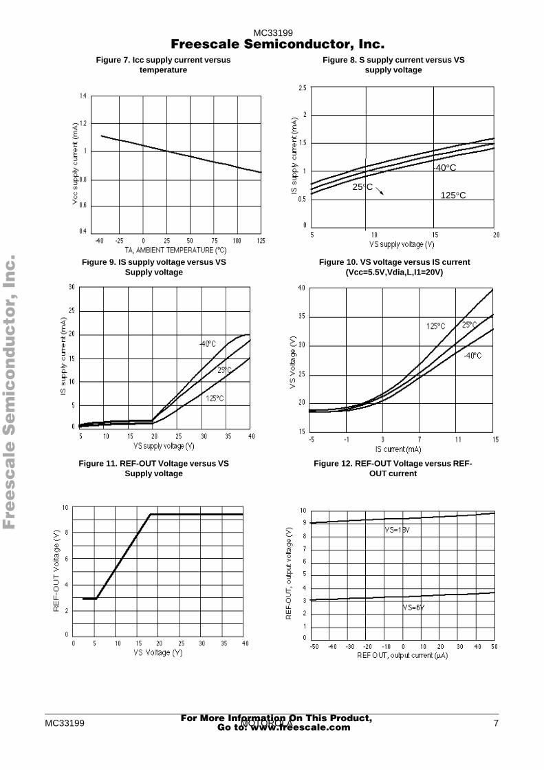
Figure 7. Icc supply current versus temperature
Figure 8. S supply current versus VS supply voltage
Figure 9. IS supply voltage versus VS Supply voltage
Figure 10. VS voltage versus IS current (Vcc=5.5V,Vdia,L,I1=20V)
Figure 11. REF-OUT Voltage versus VS Supply voltage
Figure 12. REF-OUT Voltage versus REF-OUT current
-40°C
125°C25°C
Fre
esc
ale
Se
mic
on
du
cto
r, I
Freescale Semiconductor, Inc.
For More Information On This Product, Go to: www.freescale.com
nc
...

MC33199 MOTOROLA 8
MC33199
Figure 13. L and DIA hysteresis versus temperature Figure 14. L and DIA current versus L and DIA voltage
Figure 15. DIA saturation voltage versus temperature Figure 16. DIA current limit versus temperature
Figure 17. RXD pull-up resistor versus temperature Figure 18. TXD and LO saturation voltage versus temperature
I DIA = 40mA
RXD
LO
Fre
esc
ale
Se
mic
on
du
cto
r, I
Freescale Semiconductor, Inc.
For More Information On This Product, Go to: www.freescale.com
nc
...

MC33199 MOTOROLA 9
MC33199
Figure 19. I1 saturation voltage versus temperature
Figure 20. I1 Output DC Current versus temperature
Figure 21. I1 Output Pulse Current versus VS Supply Voltage
Figure 22. I1 Pulse current width versus temperature
Figure 23. Test circuit for transient Schaffner pulses
Test pulses are directly applied to Vs and via a capacitor of 1nF to DIA and L. The voltage Vs is limited to -2V/38V by the transient suppressor diode D1. Pulses
can occur simultaneously or separately.
+12V
I1
DIA
GND
Vbat
L
Schaffner
Generator
2x1nF
2x330pF
100nF
D2
D1
I=40mAI=2mA
Fre
esc
ale
Se
mic
on
du
cto
r, I
Freescale Semiconductor, Inc.
For More Information On This Product, Go to: www.freescale.com
nc
...

MC33199 MOTOROLA 10
MC33199
DEVICE DESCRIPTION
Introduction
The MC33199D is a serial interface circuit used in diag-nostic applications. It is the interface between the microcon-troller and the special K and L lines of the ISO diagnosticport. The MC33199D has been designed to meet the «Diag-nosis System ISO9141» specification.
This product description will detail the functionality of thedevice (see simplified block diagram). First, the power supplyand reference voltage generator will be discussed, then thepaths functions between MCU, K and L lines will be detailed.A dedicated paragraph will tell about the special functionalityof the I1 pin, which allow high Baud rates transmission.
Power supplies and reference voltageThe device has two power supplies : A 5V supply, Vcc, normally connected to the MCU supply
voltage. This pin sink typically 1mA during operation. A Vbatsupply voltage, VS, normally tied to the car battery voltage.This pin can sustain up to 40V DC. Care should be taken forreverse battery protection and transient voltages higher than40V.
The voltage reference generator is supplied from both Vccand Vbat. It provides reference voltage for the K and L linescomparators thresholds. The reference voltage is dependanton Vbat voltage : it is linear versus Vbat voltage, for Vbatfrom 5,6V to 18V. Below 5.6V and over 18V the referencevoltage is clamped (see fig 11). The reference is connectedexternally to the device, through REF-OUT pin. It is availablefor other needs. It can supplied 50uA max (see fig 12).
Path functions between MCU, K and L linesThe path function from the MCU to the K line is composed
of a driver interfacing directly with the MCU through the TXDpin. The TXD pin is CMOS compatible. This driver controls apower transistor which can be turned ON or OFF. When it isON, it pull the DIA pin low. This pin is known as K line in theISO 9141 specification. The DIA pin structure is open collec-tor, without pull up component. This allow the connection ofseveral MC33199 on the K line and the use of a single pullup resistor per system (see fig 6). In order to protect the DIApin against short circuits to Vbat, the device incorporates acurrent limitation (see fig 16) and a thermal shutdown. Thiscurrent limitation will also act when the device drives a K linebus exhibiting large parasitic capacitor value (see Specialfunctionality of I1 pin below).
The path from this DIA pin, or K line, to the MCU is donethrough a comparator. The comparator threshold voltage isconnected to REF-IN-K pin. It can be tied to the REF-OUTvoltage, if the Vbat dependant threshold to be achieved. Thesecond input of this comparator is internally connected toDIA pin. The output of the comparator is available on RXDoutput pin, normally connected to a MCU I/O port. RXD pinhas a 2kOhms internal pull up resistor.
The path from the L line, used during wake-up sequence of
the transmission, to the MCU is done through a second com-parator. The comparator threshold voltage is connected toREF-IN-L pin. As the REF-IN-K pin, it can be tied to the REF-OUT voltage, if the Vbat dependant threshold need to beachieved. The second input of this comparator is internallyconnected to L pin. The output of the comparator is availableon LO output pin, which is an open collector structure. LO isnormally connected to a MCU I/O port.
The DIA, and L pins can sustain up to 38V DC. Careshould be taken for reverse battery protection and transientvoltages higher than 38V.
The DIA and L pins both have internal pull down currentsource of typically 7,5uA (see fig 14). So the L line exhibits a10uA pull down current. The DIA pin has the same behaviourwhen it is in OFF state, that is when TXD is at logic highlevel.
Special functionality of I1 pinThe MC33199D has a unique feature which allow the
transmission Baud rate to be up to 200kBauds. In practice,the K line can be several meters long, and thus can have alarge parasitic capacitor value. This parasitic capacitor valuewill slow down the low to high transition of the K line, andindeed will limit the Baud rate transmission. For the K line togo from low to high level, the parasitic capacitor need to becharged, and it can only be charged by the pull up resistor. Alow pull up resistor value would result in fast charge time ofthe capacitor, but also in large output current, and largepower dissipation in the driver.
To avoid this problem, the MC33199D incorporates adynamic current source, which is temporary activated at thelow to high transition of the TXD pin, that is when the DIA pinor K line should switch from low to high level (see fig 3 & 4).
This current source is available at I1 pin. It has a typicalvalue of 80mA. It is activated for 4us (see fig 21 & 22) and isautomatically disabled after this time. During that time it willcharge the K line parasitic capacitor. This extra current willquickly rise the K line voltage up to the Vbat, and will result inreduce rise time on the K line. With this feature theMC33199D can ensure Baud rate transmission of up to200kBauds.
During high to low transition on the K line, the parasiticcapacitor of the bus line will be discharged by the outputtransistor of the DIA pin. In this case, the total current mayexceed the internal current limitation of the DIA pin. If so, thecurrent limitation will act, and discharge current will be lim-ited to typically 60mA (See fig 4 & 16).
If a high Baud rate is necessary, the I1 pin need to be con-nected to the DIA as shown in the typical application fig 5.The I1 pin can also be left open, if the I1 functionality andhigh Baud rate are not suited in the application.
Fre
esc
ale
Se
mic
on
du
cto
r, I
Freescale Semiconductor, Inc.
For More Information On This Product, Go to: www.freescale.com
nc
...

MC33199 MOTOROLA 11
MC33199
PIN FUNCTION DESCRIPTION
Pin 1 : Vcc5V typical power supply pin. Typical supply current is less
than 1.5mA.
Pin 2 : REF-IN-LInput reference for C2 comparator. This input can be con-
nected directly to REF-OUT, with or without a resistor net-work, or to an external reference.
Pin 3 : REF-IN-KInput reference for C1 comparator. This input can be con-
nected directly to REF-OUT, with or without a resistor net-work, or to an external reference.
Pin 4 : LOOutput of C2 comparator, normally connected to a micro-
controller I/O. If L input > (Ref-in-l + Hyst/2) then output LO isin high state. If L< (Ref-in-l - Hyst/2) then output LO is in lowstate, output transistor ON.
This pin is an open collector structure. A Pull up resistorshould be added to Vcc.
Drive capability of this output is 5mA.
Pin 5 : RXDReceive output, normally connected to a microcontroller I/
O. If DIA input > (Ref-in-l + Hyst/2) then output LO is in high
state.If DIA < (Ref-in-l - Hyst/2) then output LO is in low state,
output transistor ON. This pin has an internal pull up resistorto Vcc (2KΩ typ). Drive capability of this output is 5mA
Pin 6 : TXDTransmission input, normally connected to a microcontrol-
ler I/O.This pin control DIA output. If Txd is high the outputDIA transistor is OFF. If Txd is low the DIA output transistoris ON.
Pin 9 : DIAInput / Output Diagnosis Bus line pin. This pin is an open
collector structure, protected against over current and short
circuit to Vbat (Vs). When turning ON (Txd low), this pin willpull the Bus line to Gnd, the current into DIA will be internallylimited to 60mA typ.
The internal power transistor has a thermal shutdown cir-cuit, which forces the DIA output OFF in case of over tem-perature.
DIA is also the C1 comparator input. It is protected againstboth positive and negative over voltage by a 38V zenerdiode. This pin exhibits a constant input current of 7,5µA.
Pin 10 : GNDGnd reference for the entire device.
Pin 11 : I1Bus source current pin. It is normally tied to DIA pin and to
the Bus line.At static HIGH or LOW level Txd, the current source I1
delivers a current of 3mA (typ). Only during LOW to HIGHtransition, does this current increase to a higher value inorder to charge the key line capacitor (Cl<4nF) in a shorttime (see fig 3 and 4).
Pin 12 : LInput for C2 comparator. This pin is protected against both
positive and negative over voltage by a 38V zener diode.This L line is a second independent input. It can be used
for wake up sequence in ISO diagnosis or as an additionalinput bus line.
This pin exhibits a constant input current of 7.5µA.
Pin 13 : VS12V typical, or Vbat supply pin for the device. This pin is
protected against over voltage transients.
Pin 14 : REF-OUTInternal reference voltage generator output pin. Its value
depends on Vs (Vbat) values. This output can be directlyconnected to REF-IN L and REF-IN-K, or through a resistornetwork. Maximum current capability is 50µA.
Fre
esc
ale
Se
mic
on
du
cto
r, I
Freescale Semiconductor, Inc.
For More Information On This Product, Go to: www.freescale.com
nc
...

MC33199 MOTOROLA 12
MC33199
Motorola reserves the right to make changes without further notice to any products herein to improve reliability,function or design. Motorola does not assume any liability arising out of the application or use of any product or circuitdescribed herein ; neither does it convert any licence under its patent rights of others. Motorola products are notauthorized for use as components in life support devices or systems intended for surgical implant into the body orintended to support or sustain life. Buyer agrees to notify Motorola of any such intended end use whereupon Motorolashall determine availability and suitability of its products for the use intended. Motorola and are registeredtrademarks of Motorola, Inc. Motorola, Inc. is an Equal Employment opportunity/Affirmative Action Employer.
Fre
esc
ale
Se
mic
on
du
cto
r, I
Freescale Semiconductor, Inc.
For More Information On This Product, Go to: www.freescale.com
nc
...