Automotive-grade 390 V internally clamped IGBT ESCIS 300 mJ
20
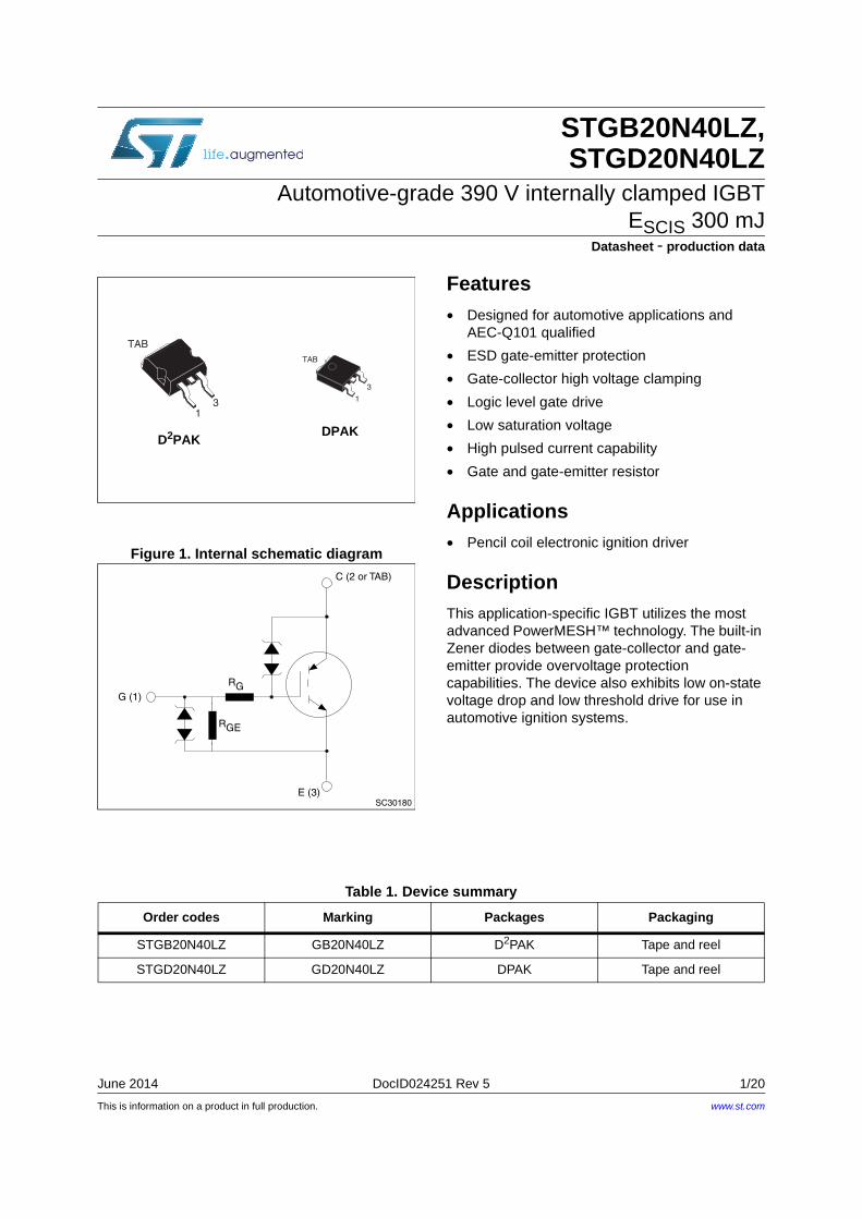
This is information on a product in full production. June 2014 DocID024251 Rev 5 1/20 STGB20N40LZ, STGD20N40LZ Automotive-grade 390 V internally clamped IGBT E SCIS 300 mJ Datasheet - production data Figure 1. Internal schematic diagram Features • Designed for automotive applications and AEC-Q101 qualified • ESD gate-emitter protection • Gate-collector high voltage clamping • Logic level gate drive • Low saturation voltage • High pulsed current capability • Gate and gate-emitter resistor Applications • Pencil coil electronic ignition driver Description This application-specific IGBT utilizes the most advanced PowerMESH™ technology. The built-in Zener diodes between gate-collector and gate- emitter provide overvoltage protection capabilities. The device also exhibits low on-state voltage drop and low threshold drive for use in automotive ignition systems. D 2 PAK DPAK 1 3 TAB 1 3 TAB C (2 or TAB) E (3) G (1) R G R GE SC30180 Table 1. Device summary Order codes Marking Packages Packaging STGB20N40LZ GB20N40LZ D 2 PAK Tape and reel STGD20N40LZ GD20N40LZ DPAK Tape and reel www.st.com
Transcript of Automotive-grade 390 V internally clamped IGBT ESCIS 300 mJ
This is information on a product in full production.
June 2014 DocID024251 Rev 5 1/20
STGB20N40LZ, STGD20N40LZ
Automotive-grade 390 V internally clamped IGBT ESCIS 300 mJ
Datasheet - production data
Figure 1. Internal schematic diagram
Features• Designed for automotive applications and
AEC-Q101 qualified
• ESD gate-emitter protection
• Gate-collector high voltage clamping
• Logic level gate drive
• Low saturation voltage
• High pulsed current capability
• Gate and gate-emitter resistor
Applications• Pencil coil electronic ignition driver
DescriptionThis application-specific IGBT utilizes the most advanced PowerMESH™ technology. The built-in Zener diodes between gate-collector and gate-emitter provide overvoltage protection capabilities. The device also exhibits low on-state voltage drop and low threshold drive for use in automotive ignition systems.
D2PAKDPAK
13
TAB
1
3
TAB
C (2 or TAB)
E (3)
G (1)RG
RGE
SC30180
Table 1. Device summary
Order codes Marking Packages Packaging
STGB20N40LZ GB20N40LZ D2PAK Tape and reel
STGD20N40LZ GD20N40LZ DPAK Tape and reel
www.st.com

Contents STGB20N40LZ, STGD20N40LZ
2/20 DocID024251 Rev 5
Contents
1 Electrical ratings . . . . . . . . . . . . . . . . . . . . . . . . . . . . . . . . . . . . . . . . . . . . 3
2 Electrical characteristics . . . . . . . . . . . . . . . . . . . . . . . . . . . . . . . . . . . . . 4
2.1 Electrical characteristics (curves) . . . . . . . . . . . . . . . . . . . . . . . . . . . . . . . . 6
3 Test circuits . . . . . . . . . . . . . . . . . . . . . . . . . . . . . . . . . . . . . . . . . . . . . . . 9
4 Package mechanical data . . . . . . . . . . . . . . . . . . . . . . . . . . . . . . . . . . . . 10
5 Packaging mechanical data . . . . . . . . . . . . . . . . . . . . . . . . . . . . . . . . . . 16
6 Revision history . . . . . . . . . . . . . . . . . . . . . . . . . . . . . . . . . . . . . . . . . . . 19

DocID024251 Rev 5 3/20
STGB20N40LZ, STGD20N40LZ Electrical ratings
20
1 Electrical ratings
Table 2. Absolute maximum ratings
Symbol ParameterValue
UnitDPAK D2PAK
VCES Collector-emitter voltage (vGE = 0) VCES(clamped) V
VECS Emitter collector voltage (VGE = 0) 20 V
IC Collector current (continuous) at TC = 100 °C 25 A
ICP (1)
1. Pulse width limited by maximum junction temperature.
Pulsed collector current 40 A
VGE Gate-emitter voltage VGE(clamped) V
PTOT Total dissipation at TC = 25 °C 125 150 W
ESCIS Single pulse energy TC = 25 °C, L = 3 mH, VCC = 50 V 300 mJ
ESCIS Single pulse energy TC =150 °C, L = 3 mH, VCC = 50 V 180 mJ
ESD
Human body model, R= 1.5 kΩ, C = 100 pF 8 kV
Machine model, R = 0, C = 100 pF 600 V
Charged device model 4 kV
Tstg Storage temperature– 55 to 175 °C
Tj Operating junction temperature
Table 3. Thermal data
Symbol ParameterValue
UnitDPAK D2PAK
Rthj-case Thermal resistance junction-case 1.2 1 °C/W
Rthj-amb Thermal resistance junction-ambient 100 62.5 °C/W

Electrical characteristics STGB20N40LZ, STGD20N40LZ
4/20 DocID024251 Rev 5
2 Electrical characteristics
TJ = 25 °C unless otherwise specified.
Table 4. Static electrical characteristics
Symbol Parameter Test conditions Min. Typ. Max. Unit
VCES(clamped)
Collector emitter clamped voltage (VGE = 0)
IC = 2 mA 390 V
IC = 2 mA, TJ = - 40 °C to 175 °C 365 425 V
VECS
Emitter collector break-down voltage (VGE = 0)
IC = 75 mA 28 V
IC = 75 mATJ = - 40 °C to 175 °C
20 V
VGE(clamped)Gate emitter clamped voltage
IG = ±2 mATJ = - 40 °C to 175 °C
12 16 V
ICES
Collector cut-off current(VGE = 0)
VCE = 15 V, TJ = 175 °C 20 µA
VCE = 200 V, TJ = 175 °C 100 µA
IGES
Gate-emitter leakage current (VCE = 0)
VGE = ±10 V 625 µA
VGE = ±10 VTJ = - 40 °C to 175 °C
450 900 µA
RGEGate emitter resistance
11 16 22 kΩ
RG Gate resistance 100 Ω
VGE(th)Gate threshold voltage
VGE =VCE, IC = 1 mA 1.5 1.95 2.5 V
VGE =VCE, IC = 1 mA, TJ = 175 °C 0.85 1.3 1.7 V
VCE(sat)Collector emitter saturation voltage
VGE = 4.5 V, IC = 10 A,TJ = 175 °C
1.5 1.8 V
VGE = 4 V, IC = 6 A, 1.30 1.6 V
gfeForward transconductance
VCE = 25 V, IC = 10 A 10.3 S
Table 5. Dynamic electrical characteristics
Symbol Parameter Test conditions Min. Typ. Max. Unit
Cies Input capacitance
VCE = 25 V, f = 1 MHz,VGE = 0
- 910 - pF
Coes Output capacitance - 70 - pF
CresReverse transfer capacitance
- 10 - pF
Qg Gate chargeVCE = 280 V, IC = 10 A,
VGE = 5 V- 24 - nC
DocID024251 Rev 5 5/20
STGB20N40LZ, STGD20N40LZ Electrical characteristics
20
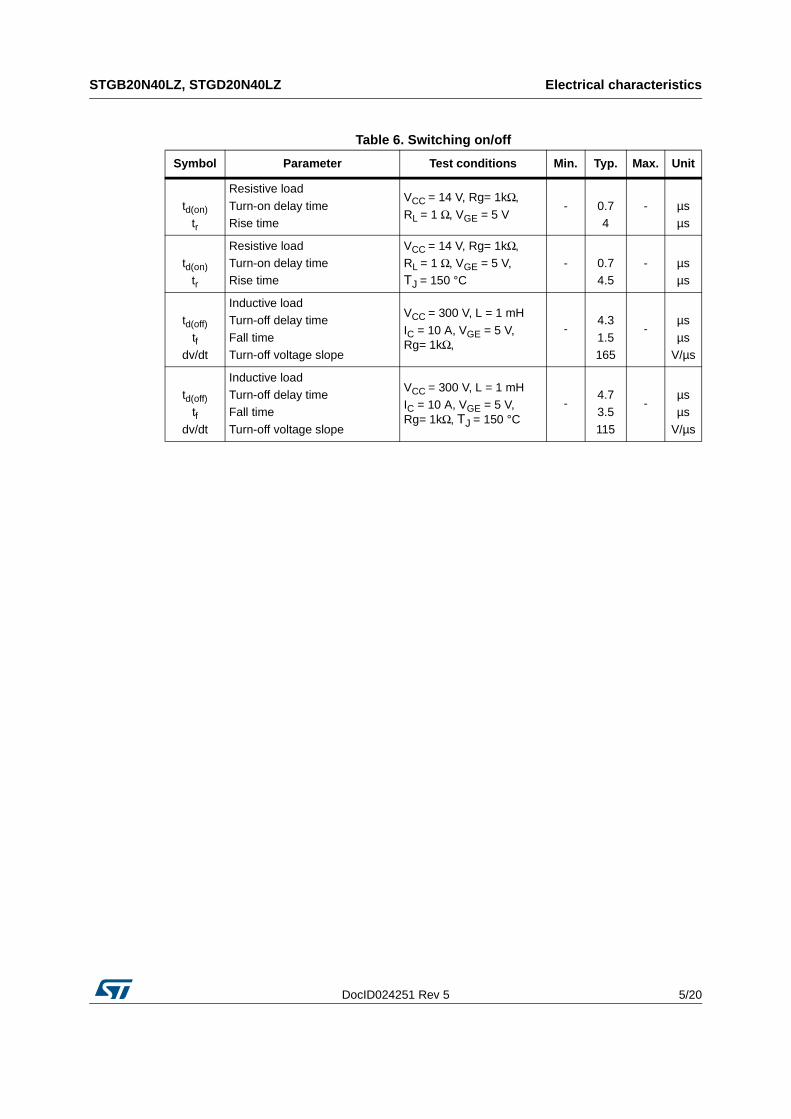
Table 6. Switching on/off
Symbol Parameter Test conditions Min. Typ. Max. Unit
td(on)
tr
Resistive load
Turn-on delay timeRise time
VCC = 14 V, Rg= 1kΩ,
RL = 1 Ω, VGE = 5 V- 0.7
4- µs
µs
td(on)
tr
Resistive loadTurn-on delay timeRise time
VCC = 14 V, Rg= 1kΩ,RL = 1 Ω, VGE = 5 V,TJ = 150 °C
- 0.74.5
- µsµs
td(off)
tfdv/dt
Inductive loadTurn-off delay time
Fall timeTurn-off voltage slope
VCC = 300 V, L = 1 mH
IC = 10 A, VGE = 5 V, Rg= 1kΩ,
-4.3
1.5165
-µs
µsV/µs
td(off)
tfdv/dt
Inductive loadTurn-off delay timeFall time
Turn-off voltage slope
VCC = 300 V, L = 1 mHIC = 10 A, VGE = 5 V, Rg= 1kΩ, TJ = 150 °C
-4.73.5
115
-µsµs
V/µs

Electrical characteristics STGB20N40LZ, STGD20N40LZ
6/20 DocID024251 Rev 5
2.1 Electrical characteristics (curves)
Figure 2. Collector-emitter on voltage vs temperature (Vge= 4.5 V)
Figure 3. Collector-emitter on voltage vs temperature (IC= 6 A)
Figure 4. Collector-emitter on voltage vs temperature (IC= 10 A)
Figure 5. Self clamped inductive switch
Vce(sat)
1.75
1.5
1.25
1-100 0 TJ(°C)
(V)
-50 15050 100
2
IC= 6A
IC= 10A
IC= 15A
GIPD170620131357FSR Vce(sat)
1.35
1.25
1.15
1.05-100 0 TJ(°C)
(V)
-50 15050 100
1.45 Vge= 3.8V
Vge= 4.5V
Vge= 5.0V
GIPD180620131124FSR
Vce(sat)
1.7
1.5
1.3
1.1-100 0 TJ(°C)
(V)
-50 15050 100
1.9 Vge= 3.8V
Vge= 4.5V
Vge= 5.0V
GIPD180620131131FSRISCIS
10
10.1 L(mH)
(A)
1
TJ= 150°C
TJ= 25°C
VCE = 13 VVGE = 5 VRG = 1 kΩ
GIPD180620131141FSR

DocID024251 Rev 5 7/20
STGB20N40LZ, STGD20N40LZ Electrical characteristics
20
Figure 6. Output characteristics (TJ= 25 °C) Figure 7. Output characteristics (TJ= -40 °C)
Figure 8. Output characteristics (TJ= 175 °C) Figure 9. Transfer characteristics
Figure 10. Collector cut-off current vs. temperature
Figure 11. Normalized collector emitter voltage vs temperature
IC
5
10
0 VCE(V)
(A)
2
VGE= 3.5V
15
20
25
30
35
40
45
4 6 8 10
4.0V
4.5V
5.0V
5.5V
6.0V
6.5V
7.0V
7.5V
GIPD180620131201FSRIC
10
0 VCE(V)
(A)
2
VGE= 3.5V
20
30
40
50
4 6 8 10
4.0V
4.5V
5.0V
5.5V6.0V
6.5V
7.0V
7.5V
GIPD180620131405FSR
IC
0 VCE(V)
(A)
2
VGE= 3.5V
4 6 8 10
4.0V
4.5V
5.0V
5.5V6.0V6.5V
7.0V
7.5V
5
10
15
20
25
30
35
40
45
GIPD180620131411FSRIC
0VGE(V)
(A)
2 3 4 5 6
TJ= 175°C
10
20
30
40
50
71
TJ= 25°C
TJ= -40°C
VCE= 15 V
GIPD180620131417FSR
ICES
0.1-50 50 TJ(°C)
(µA)
0 100 150
VCE= 350V
1
10
VCE= 200V
GIPD170620131412FSR VCES
0.98-100 0 TJ(°C)
(norm)
-50 15050 100
IC= 2mA
0.99
1
1.05
GIPD1706201314125SR

Electrical characteristics STGB20N40LZ, STGD20N40LZ
8/20 DocID024251 Rev 5
Figure 12. Normalized gate threshold voltage vs temperature
Figure 13. Normalized collector emitter on- voltage vs temperature
Figure 14. Thermal impedance for D²PAK Figure 15. Thermal impedance for DPAK
Vth
0.6-100 0 TJ(°C)
(norm)
-50 15050 100
0.8
1
VGE = VCE
IC = 1mA
GIPD1706201314132SRVce(sat)
0.85TJ(°C)
(norm)
-50 0 50 100 150
VGE= 4.5VIC= 10A
0.9
0.95
1
1.05
1.1
-100
GIPD180620131434FSR
DocID024251 Rev 5 9/20
STGB20N40LZ, STGD20N40LZ Test circuits
20
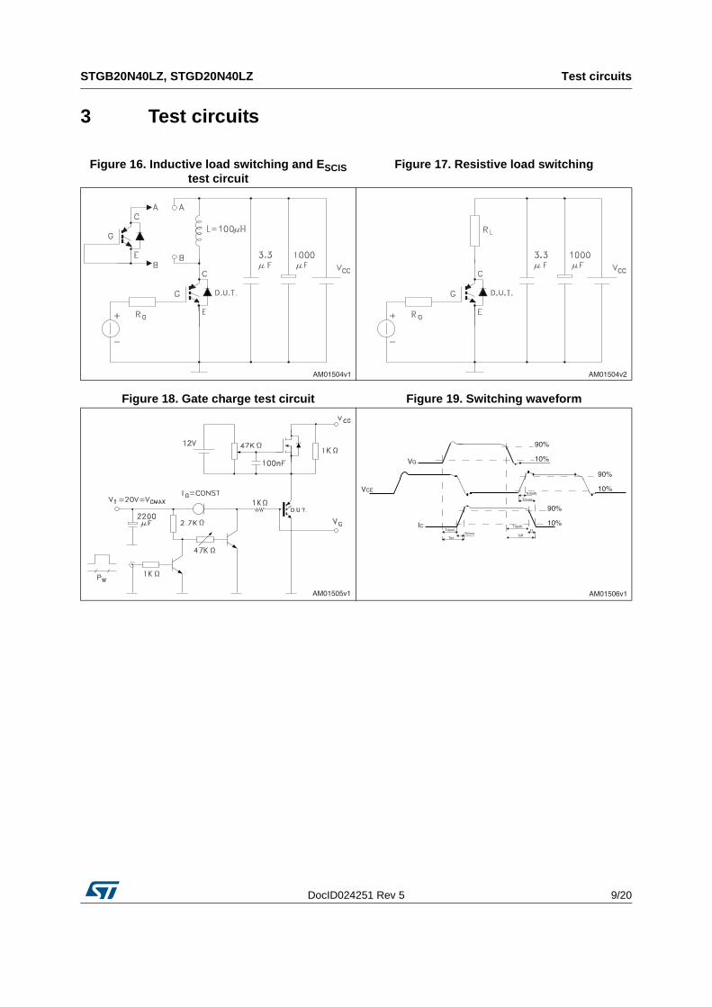
3 Test circuits
Figure 16. Inductive load switching and ESCIS test circuit
Figure 17. Resistive load switching
Figure 18. Gate charge test circuit Figure 19. Switching waveform
AM01504v1 AM01504v2
L
AM01505v1 AM01506v1
90%
10%
90%
10%
VG
VCE
ICTd(on)
TonTr(Ion)
Td(off)
Toff
Tf
Tr(Voff)
Tcross
90%
10%

Package mechanical data STGB20N40LZ, STGD20N40LZ
10/20 DocID024251 Rev 5
4 Package mechanical data
In order to meet environmental requirements, ST offers these devices in different grades of ECOPACK® packages, depending on their level of environmental compliance. ECOPACK® specifications, grade definitions and product status are available at: www.st.com. ECOPACK® is an ST trademark.
Figure 20. D²PAK (TO-263) drawing
0079457_T

DocID024251 Rev 5 11/20
STGB20N40LZ, STGD20N40LZ Package mechanical data
20
Table 7. D²PAK (TO-263) mechanical data
Dim.mm
Min. Typ. Max.
A 4.40 4.60
A1 0.03 0.23
b 0.70 0.93
b2 1.14 1.70
c 0.45 0.60
c2 1.23 1.36
D 8.95 9.35
D1 7.50
E 10 10.40
E1 8.50
e 2.54
e1 4.88 5.28
H 15 15.85
J1 2.49 2.69
L 2.29 2.79
L1 1.27 1.40
L2 1.30 1.75
R 0.4
V2 0° 8°

Package mechanical data STGB20N40LZ, STGD20N40LZ
12/20 DocID024251 Rev 5
Figure 21. D²PAK footprint(a)
a. All dimension are in millimeters
16.90
12.20
9.75
3.50
5.08
1.60
Footprint

DocID024251 Rev 5 13/20
STGB20N40LZ, STGD20N40LZ Package mechanical data
20
Figure 22. DPAK (TO-252) type A drawing
0068772_M_type_A

Package mechanical data STGB20N40LZ, STGD20N40LZ
14/20 DocID024251 Rev 5
Table 8. DPAK (TO-252) type A mechanical data
Dim.mm
Min. Typ. Max.
A 2.20 2.40
A1 0.90 1.10
A2 0.03 0.23
b 0.64 0.90
b4 5.20 5.40
c 0.45 0.60
c2 0.48 0.60
D 6.00 6.20
D1 5.10
E 6.40 6.60
E1 4.70
e 2.28
e1 4.40 4.60
H 9.35 10.10
L 1.00 1.50
(L1) 2.80
L2 0.80
L4 0.60 1.00
R 0.20
V2 0° 8°

DocID024251 Rev 5 15/20
STGB20N40LZ, STGD20N40LZ Package mechanical data
20
Figure 23. DPAK (TO-252) type A footprint (b)
b. All dimensions are in millimeters
Footprint_REV_M_type_A

Packaging mechanical data STGB20N40LZ, STGD20N40LZ
16/20 DocID024251 Rev 5
5 Packaging mechanical data
Figure 24. Tape drawing
P1A0 D1
P0
F
W
E
D
B0K0
T
User direction of feed
P2
10 pitches cumulativetolerance on tape +/- 0.2 mm
User direction of feed
R
Bending radius
B1
For machine ref. onlyincluding draft andradii concentric around B0
AM08852v1
Top covertape

DocID024251 Rev 5 17/20
STGB20N40LZ, STGD20N40LZ Packaging mechanical data
20
Figure 25. Reel drawing
Table 9. D²PAK (TO-263) tape and reel mechanical data
Tape Reel
Dim.mm
Dim.mm
Min. Max. Min. Max.
A0 10.5 10.7 A 330
B0 15.7 15.9 B 1.5
D 1.5 1.6 C 12.8 13.2
D1 1.59 1.61 D 20.2
E 1.65 1.85 G 24.4 26.4
F 11.4 11.6 N 100
K0 4.8 5.0 T 30.4
P0 3.9 4.1
P1 11.9 12.1 Base qty 1000
P2 1.9 2.1 Bulk qty 1000
R 50
T 0.25 0.35
W 23.7 24.3
A
D
B
Full radius G measured at hub
C
N
REEL DIMENSIONS
40mm min.
Access hole
At sl ot location
T
Tape slot in core fortape start 25 mm min.width
AM08851v2

Packaging mechanical data STGB20N40LZ, STGD20N40LZ
18/20 DocID024251 Rev 5
Table 10. DPAK (TO-252) tape and reel mechanical data
Tape Reel
Dim.mm
Dim.mm
Min. Max. Min. Max.
A0 6.8 7 A 330
B0 10.4 10.6 B 1.5
B1 12.1 C 12.8 13.2
D 1.5 1.6 D 20.2
D1 1.5 G 16.4 18.4
E 1.65 1.85 N 50
F 7.4 7.6 T 22.4
K0 2.55 2.75
P0 3.9 4.1 Base qty. 2500
P1 7.9 8.1 Bulk qty. 2500
P2 1.9 2.1
R 40
T 0.25 0.35
W 15.7 16.3

DocID024251 Rev 5 19/20
STGB20N40LZ, STGD20N40LZ Revision history
20
6 Revision history
Table 11. Document revision history
Date Revision Changes
08-Feb-2013 1 Initial release.
24-Jun-2013 2
Added device in D2PAK.
Modified Table 1: Device summary.Added Section 2.1: Electrical characteristics (curves).Updated Section 4: Package mechanical data and Section 5: Packaging mechanical data.Minor text changes.
25-Sep-2013 3Updated td(on) value for resistive load in Table 6: Switching on/off.Updated mechanical data for DPAK.
Minor text changes.
14-Jan-2014 4
Modified title in cover page.
Added: ESCIS in Table 2, VECS and gfs values in Table 4.Modified minimum value of VGE(clamped) in Table 4
Updated Section 4: Package mechanical data
Modified order codes in Table 1.Minor text changes.
4-Jun-2014 5 Updated features in cover page.
STGB20N40LZ, STGD20N40LZ
20/20 DocID024251 Rev 5
Please Read Carefully:
Information in this document is provided solely in connection with ST products. STMicroelectronics NV and its subsidiaries (“ST”) reserve theright to make changes, corrections, modifications or improvements, to this document, and the products and services described herein at anytime, without notice.
All ST products are sold pursuant to ST’s terms and conditions of sale.
Purchasers are solely responsible for the choice, selection and use of the ST products and services described herein, and ST assumes noliability whatsoever relating to the choice, selection or use of the ST products and services described herein.
No license, express or implied, by estoppel or otherwise, to any intellectual property rights is granted under this document. If any part of thisdocument refers to any third party products or services it shall not be deemed a license grant by ST for the use of such third party productsor services, or any intellectual property contained therein or considered as a warranty covering the use in any manner whatsoever of suchthird party products or services or any intellectual property contained therein.
UNLESS OTHERWISE SET FORTH IN ST’S TERMS AND CONDITIONS OF SALE ST DISCLAIMS ANY EXPRESS OR IMPLIEDWARRANTY WITH RESPECT TO THE USE AND/OR SALE OF ST PRODUCTS INCLUDING WITHOUT LIMITATION IMPLIEDWARRANTIES OF MERCHANTABILITY, FITNESS FOR A PARTICULAR PURPOSE (AND THEIR EQUIVALENTS UNDER THE LAWSOF ANY JURISDICTION), OR INFRINGEMENT OF ANY PATENT, COPYRIGHT OR OTHER INTELLECTUAL PROPERTY RIGHT.
ST PRODUCTS ARE NOT DESIGNED OR AUTHORIZED FOR USE IN: (A) SAFETY CRITICAL APPLICATIONS SUCH AS LIFESUPPORTING, ACTIVE IMPLANTED DEVICES OR SYSTEMS WITH PRODUCT FUNCTIONAL SAFETY REQUIREMENTS; (B)AERONAUTIC APPLICATIONS; (C) AUTOMOTIVE APPLICATIONS OR ENVIRONMENTS, AND/OR (D) AEROSPACE APPLICATIONSOR ENVIRONMENTS. WHERE ST PRODUCTS ARE NOT DESIGNED FOR SUCH USE, THE PURCHASER SHALL USE PRODUCTS ATPURCHASER’S SOLE RISK, EVEN IF ST HAS BEEN INFORMED IN WRITING OF SUCH USAGE, UNLESS A PRODUCT ISEXPRESSLY DESIGNATED BY ST AS BEING INTENDED FOR “AUTOMOTIVE, AUTOMOTIVE SAFETY OR MEDICAL” INDUSTRYDOMAINS ACCORDING TO ST PRODUCT DESIGN SPECIFICATIONS. PRODUCTS FORMALLY ESCC, QML OR JAN QUALIFIED AREDEEMED SUITABLE FOR USE IN AEROSPACE BY THE CORRESPONDING GOVERNMENTAL AGENCY.
Resale of ST products with provisions different from the statements and/or technical features set forth in this document shall immediately voidany warranty granted by ST for the ST product or service described herein and shall not create or extend in any manner whatsoever, anyliability of ST.
ST and the ST logo are trademarks or registered trademarks of ST in various countries.Information in this document supersedes and replaces all information previously supplied.
The ST logo is a registered trademark of STMicroelectronics. All other names are the property of their respective owners.
© 2014 STMicroelectronics - All rights reserved
STMicroelectronics group of companies
Australia - Belgium - Brazil - Canada - China - Czech Republic - Finland - France - Germany - Hong Kong - India - Israel - Italy - Japan - Malaysia - Malta - Morocco - Philippines - Singapore - Spain - Sweden - Switzerland - United Kingdom - United States of America
www.st.com