Auto 40-V to 1-kV Input Flyback Design Supporting ... · Regenerative Braking Safety Test TI...
41
1 2 3 5 4 6 7 VBIAS1 = 20 V VBIAS2 = –5 V UCC28C43-Q1 Flyback Controller Gate Vcc Start-up Circuit SiC Optocoupler COMP VIN = 40 V to 1000 V Optional Level Shifter LOUT TL431A-Q1 VOUT = 15 V Average current = 4 A Copyright © 2018, Texas Instruments Incorporated 1 TIDUDT5 – February 2018 Submit Documentation Feedback Copyright © 2018, Texas Instruments Incorporated Automotive 40-V to 1-kV Input Flyback Reference Design Supporting Regenerative Braking Safety Test TI Designs: TIDA-01505 Automotive 40-V to 1-kV Input Flyback Reference Design Supporting Regenerative Braking Safety Test Description This power supply reference design for automotive auxiliary circuits generates a 15-V, 4-A output from a wide input range of 40 V to 1 kV and up to a 1.2-kV transient. The design fits ideally into an 800-V battery- driven hybrid-electric vehicle (HEV) or electric vehicle (EV) traction inverter system. The 40-V minimum input voltage supports the functional safety test for the regenerative braking from the traction motor. This reference design implements a silicon carbide (SiC) MOSFET with high blocking voltage and low gate charge to reduce switching losses. A non-isolated level shifter enables driving the SiC MOSFET from the Si MOSFET driver embedded in the flyback controller. The board includes two flyback converter variants: primary-side regulation (PSR) and optocoupler feedback to make comparisons and address different needs. The transformer design meets qualifications for Automotive AEC-Q200 Grade 1 with reinforced isolation. Resources TIDA-01505 Design Folder UCC28C43-Q1 Product Folder TL431-Q1 Product Folder ASK Our E2E™ Experts Features • 40-V to 1-kV input, 15-V Output Flyback Auxiliary Power Supply With Output Power up to 60 W • Regulated 15 V With Active Start-Up Circuit for Reduced Standby Power • Extendable to Higher Voltage and Higher Power Range to Utilize High-Voltage Capability of SiC MOSFET • Automotive Grade 1 Qualified Transformer With Reinforced Isolation (Qualified With 5.7-kV High- Pot Test) • Two Converter Variants With PSR and Optocoupler Feedback Included on Board • Constant Switching Frequency Type of Controller With Maximum Switching Frequency of 1 MHz and Duty Cycle Range From 0% to 96% Applications • HEV/EV Traction Inverter • HEV/EV On Board Charger • Electronic Control Units • HEV/EV DC/DC Converters
Transcript of Auto 40-V to 1-kV Input Flyback Design Supporting ... · Regenerative Braking Safety Test TI...

1
2
3
5
4
6
7VBIAS1 = 20 V
VBIAS2 = ±5 V
UCC28C43-Q1Flyback
Controller
Gate
Vcc
Start-upCircuit
SiC
OptocouplerCOMP
VIN = 40 V to 1000 V
Optional
Level Shifter
LOUT
TL431A-Q1
VOUT = 15 VAverage current = 4 A
Copyright © 2018, Texas Instruments Incorporated
1TIDUDT5–February 2018Submit Documentation Feedback
Copyright © 2018, Texas Instruments Incorporated
Automotive 40-V to 1-kV Input Flyback Reference Design SupportingRegenerative Braking Safety Test
TI Designs: TIDA-01505Automotive 40-V to 1-kV Input Flyback Reference DesignSupporting Regenerative Braking Safety Test
DescriptionThis power supply reference design for automotiveauxiliary circuits generates a 15-V, 4-A output from awide input range of 40 V to 1 kV and up to a 1.2-kVtransient. The design fits ideally into an 800-V battery-driven hybrid-electric vehicle (HEV) or electric vehicle(EV) traction inverter system. The 40-V minimum inputvoltage supports the functional safety test for theregenerative braking from the traction motor. Thisreference design implements a silicon carbide (SiC)MOSFET with high blocking voltage and low gatecharge to reduce switching losses. A non-isolated levelshifter enables driving the SiC MOSFET from the SiMOSFET driver embedded in the flyback controller.The board includes two flyback converter variants:primary-side regulation (PSR) and optocouplerfeedback to make comparisons and address differentneeds. The transformer design meets qualifications forAutomotive AEC-Q200 Grade 1 with reinforcedisolation.
Resources
TIDA-01505 Design FolderUCC28C43-Q1 Product FolderTL431-Q1 Product Folder
ASK Our E2E™ Experts
Features• 40-V to 1-kV input, 15-V Output Flyback Auxiliary
Power Supply With Output Power up to 60 W• Regulated 15 V With Active Start-Up Circuit for
Reduced Standby Power• Extendable to Higher Voltage and Higher Power
Range to Utilize High-Voltage Capability of SiCMOSFET
• Automotive Grade 1 Qualified Transformer WithReinforced Isolation (Qualified With 5.7-kV High-Pot Test)
• Two Converter Variants With PSR and OptocouplerFeedback Included on Board
• Constant Switching Frequency Type of ControllerWith Maximum Switching Frequency of 1 MHz andDuty Cycle Range From 0% to 96%
Applications• HEV/EV Traction Inverter• HEV/EV On Board Charger• Electronic Control Units• HEV/EV DC/DC Converters

System Description www.ti.com
2 TIDUDT5–February 2018Submit Documentation Feedback
Copyright © 2018, Texas Instruments Incorporated
Automotive 40-V to 1-kV Input Flyback Reference Design SupportingRegenerative Braking Safety Test
An IMPORTANT NOTICE at the end of this TI reference design addresses authorized use, intellectual property matters and otherimportant disclaimers and information.
1 System DescriptionAt the time of this writing, the latest electric cars are experiencing dramatic technological changes in thepower electronics area. The move toward 800-V technology has shown significant development amongvarious car manufacturers. In infrastructure, raising the voltage to 800 will enable significantly reducedcharging times and extend drive mileage. These developments also raise many design challenges, suchas high-voltage safety and reliability, isolation requirements, trade-offs between cost and performance,and so forth.
This reference design is a 60-W power supply which enables an ultra-wide input range from a 40-V(minimum) to 1-kV (maximum) DC voltage targeted for use in 800-V battery systems. A primary feature ofthis design is that the converter can power up at the 40-V minimum input voltage, which allows support forthe system safety test during the regenerative braking for traction inverters. This design is an auxiliarypower supply solution that generates a 15-V output for the traction inverter subsystems. The design alsoimplements reinforced isolation for safety enhancement. The single-ended, flyback topology has beenchosen due to its low cost, high isolation rating, and design simplicity. Moreover, the design includes twoonboard converter variants, with optocoupler and primary side regulation (PSR) for performancecomparisons.
Carefully consider the following criteria to fulfill the design requirements:• Voltage blocking capability of the switching device –
Because of the high voltage, the Si MOSFET, which has a lower design margin for blocking voltageand high channel resistance, is not suitable. The design requires use of an SiC MOSFET with a higherblocking capability.
• Pulse-width modulated (PWM) switching duty cycle –Support for such an ultra-wide input voltage range requires a controller that is able to operate withinthe corresponding, wide PWM duty-cycle range.
• Active start-up circuit –The traditional, resistive start-up circuit causes high quiescent losses at high input voltage. This designimplements an active start-up circuit for reduced leakage current.
• Noise coupling –The high-voltage input and fast switching of the SiC MOSFET leads to high dv/dt switching nodes,which generates a large amount of noise and antenna loops. The essential switching nodes must bekept small and away from quiet areas to reduce the noise coupling.
• Safety clearance –The distance between the high-voltage area at the primary side and low-voltage area at the secondaryside must have enough clearance to comply with safety requirements. Reinforced isolations arenormally imposed according to automotive safety requirements. The ground of the low-voltage sidemay be connected to a 12-V battery or vehicle chassis, which is touchable by the human body.
• Printed-circuit board (PCB) clearance and high-voltage components selection –The PCB clearance must be carefully designed to avoid electrical breakdown failure. Carefully selectcomponents that tolerate high voltages to properly handle the high-voltage stress.
Figure 1 shows a block diagram example of the 800-V battery-driven traction inverter system, whichhighlights the inverter stage, isolation, resolver, safety logics, current and voltage sensing. and so forth.This reference design is capable of powering up from a 40-V minimum input voltage for the purpose ofenabling engineers to work safely and allow them to test the regenerative braking mechanism.Regenerative braking utilizes the same insulated-gate bipolar transistor (IGBT)-based traction inverter toforce the power flow in the reverse direction from the motor and send the power back to the battery. TheIGBTs are controlled in a different algorithm to regulate the DC output from AC. Regenerative brakingtechnology funnels the energy created by the braking process back into the system in the form of chargingthe battery for further use. Typically, in a regenerative braking system, the energy loss from the brakingprocess transfers to the generator from the rotating axel before transferring to the battery, thus savingenergy.

12-V Battery
Transient Suppression
Reverse Polarity
Protection
DC/DC Converter
DC/DC (buck)
EN
P15V
System Basis Chip
(SBC)
TIDA-01179
1P5V
P15V
TIDA-01505
Resolver Interface
15 V
MCU
ADC
PWM
Isolation Isolation
Isolated
Driver
DC DC
6x
HV Voltage Sense
Current Sense
6x
IGBT Temp Sensing
M
R
Traction Motor
DC Link
ICBTs
Regenerating Braking
800-VBattery
Copyright © 2018, Texas Instruments Incorporated
www.ti.com System Description
3TIDUDT5–February 2018Submit Documentation Feedback
Copyright © 2018, Texas Instruments Incorporated
Automotive 40-V to 1-kV Input Flyback Reference Design SupportingRegenerative Braking Safety Test
Another TI Design, TIDA-01179, serves as the redundant supply, which is connected from the 12-Vbattery input to the TIDA-01505 output rail. As Figure 1 shows, the isolated DC/DC (TIDA-01505) and thenon-isolated DC/DC (TIDA-01179) are connected in an Oring configuration and provide the power to thedownstream loads together. The TIDA-01179 includes a buck-boost converter and a buck converter. Thisdevice is a 30-W front-end power supply and supports the cold crank operations for the 12-V car battery.The device generates various power rails across the isolation barrier and supplies them to the circuitslocated at the high-voltage side.
Figure 1. Block Diagram for 800-V Battery-Driven Inverter System and Implementation of TIDA-01505
1.1 Key System Specifications
Table 1. Key System Specifications
PARAMETER SPECIFICATIONS
Input • 40-V to 1-kV ultra-wide input• 1.2-kV transient
Output
• 15-V DC VOUT, 4-A IOUT DC continuous• 2-A maximum IOUT for the variant of PSR at 40-V input, due to regulation
degradation• Full power delivery starting from 100-V input voltage• Output power of 65 W max due to thermal constraints• Peak efficiency greater than 85%• Ripple less than 3% VOUT at full load• Load step 50% to 100% with voltage deviation of less than 15% for the PSR
flyback; voltage deviation of less than 5% for the flyback with optocoupler
Features
• Constant switching frequency type of controller operates at duty cycle rangefrom 15% to 85%
• SiC MOSFET application uses controller with Si MOSFET-integrated driver• Key components temperature rise: 40 maximum• Two design variants with comparable layout design• Automotive Grade 1-qualified transformer with reinforced isolation (tested at
5.7-kV high-pot test)

1
2
3
5
4
6
7VBIAS1 = 20 V
VBIAS2 = ±5 V
UCC28C43-Q1Flyback
Controller
Gate
Vcc
Start-upCircuit
SiC
OptocouplerCOMP
VIN = 40 V to 1000 V
Optional
Level Shifter
LOUT
TL431A-Q1
VOUT = 15 VAverage current = 4 A
Copyright © 2018, Texas Instruments Incorporated
System Overview www.ti.com
4 TIDUDT5–February 2018Submit Documentation Feedback
Copyright © 2018, Texas Instruments Incorporated
Automotive 40-V to 1-kV Input Flyback Reference Design SupportingRegenerative Braking Safety Test
2 System Overview
2.1 Block DiagramFigure 2 shows the system block diagram. The design consists of four main functional elements:• The active start-up circuit replaces the pure, high MΩ resistors circuit to ensure fewer instances of
power loss and a faster start-up time.• The flyback controller operates at an ultra-wide duty cycle switching and drives the SiC MOSFET.
Other benefits include a low part court and a single magnetic transformer for buck-boost conversion.• The non-isolated level shifter converts the PWM switching signal from the integrated Si MOSFET driver
to that of the SiC MOSFET. The requested driving voltages are +20 V and –5 V for turnon and turnoff,respectively.
• The optocoupler is optional in this design. The device closes the feedback loop and provides betterregulation performance. This reference design includes two converter versions for the purposes ofcustomer evaluation: one with an optocoupler and another with primary side regulation (PSR).
Figure 2. TIDA-01505 Block diagram

RRT
CCT
VREF
RT/CT
GND
Copyright © 2016, Texas Instruments Incorporated
8.4 mA
VDDON
VDDOFF
CCT
tONtOFF
tPERIOD
www.ti.com System Overview
5TIDUDT5–February 2018Submit Documentation Feedback
Copyright © 2018, Texas Instruments Incorporated
Automotive 40-V to 1-kV Input Flyback Reference Design SupportingRegenerative Braking Safety Test
2.2 Highlighted Products
2.2.1 UCC28C43-Q1The UCC28C43-Q1 is a high-performance, current-mode PWM controller. The BiCMOS design allowsoperation at high frequencies of at least 1 MHz that are not feasible in the predecessor bipolar devices.The low start-up current of 60 µA (typical) reduces the steady-state power dissipation in the start-upresistors and boosts the efficiency in battery-operated supplies. The BiCMOS internal reference of 2.5 Vhas an enhanced design and utilizes production trim to allow initial accuracy of ±1% at room temperatureand ±2% over the full temperature range.
2.2.2 TL431A-Q1The TL431-Q1 is a three-pin adjustable shunt regulator with a specified thermal stability over theapplicable automotive temperature ranges. The TL431-Q1 can be used as a single voltage reference,error amplifier, voltage clamp, or comparator with integrated reference. The TL431-Q1 consists of aninternal reference and amplifier that outputs a sink current based on the difference between the referencepin and the virtual internal pin. The sink current is produced by the internal Darlington pair, which allowsthis device to sink a maximum current of 100 mA.
2.3 System Design TheoryThis reference design implements the single-end flyback topology with a single switch and transformer toachieve high power density over a wide range of operating conditions. The active start-up circuitryincreases the steady-state efficiency. The use of a SiC MOSFET increases the input DC voltage range.The variant of including an optocoupler on the secondary side enables fast transient response and ahigher loop bandwidth. The variant without an optocoupler avoids life-cycle degradation in a high-temperature, harsh automotive environment.
2.3.1 Switching FrequencyThe switching frequency of the converter is chosen as 140 kHz, which is slightly below the conductedelectromagnetic interference (EMI) frequency range. The internal oscillator uses a timing capacitor (CCT)and a timing resistor (RRT) to program the oscillator frequency and maximum duty cycle (as Figure 3shows). Program the operating frequency based on the curves specified in the data sheet, where thetiming resistor can be found after selecting the timing capacitor. The best practice is to select a timingcapacitor to have a flat temperature coefficient, typical of most COG- or NPO-type capacitors. Selectvalues of 13k Ω and 1000 pF for RRT and CCT, respectively, to operate at a 140-kHz switching frequency.
Figure 3. UCC28C43-Q1 Oscillator Circuit

sec_avgpkpri_avgpk
PS
I 20 AI 1.7 A
N 12
sec_rms sec_avgpk OFF_actI I D 20 A 0.2 9 A u u
sec_avgpksec_pk
OFF_act
2 I 2 20 AI 22.3 A
2 D 2 0.2
u u
sec_avgsec_avgpk
OFF_act
I 4I 20 A
D 0.2
OUTsec_avg
OUT
PI 4 A
V
OFF_act ON_actD 1 D 0.2
OUT f PSON_act
OUT f PS
V V ND 0.8
VIN_min V V N
u
u
IN_minPS
OUT
V DN 14.1
V 1 D u
ON
OFF
TD
T
IN_min ON OUT OFF PSV T V T Nu u u
System Overview www.ti.com
6 TIDUDT5–February 2018Submit Documentation Feedback
Copyright © 2018, Texas Instruments Incorporated
Automotive 40-V to 1-kV Input Flyback Reference Design SupportingRegenerative Braking Safety Test
2.3.2 Transformer DesignIf ignoring the drop voltage across the switching MOSFET and output rectification diode, calculate thewinding turns ratio as:
(1)
where,• VIN_min is the minimum input voltage,• TON is the switch-on time of the switching MOSFET,• TOFF is the OFF time of the switching MOSFET,• NPS is the turn ratio between the primary turns and secondary turns of the transformer.
The converter targets a full power delivery when the input voltage reaches 50 V; therefore, performcalculations with 50 V as the minimum input voltage. Considering
(2)
is the duty cycle, and the maximum duty cycle is chosen as 85%. Therefore, calculate the turn ratio of thetransformer primary winding to the secondary winding (NPS) as:
(3)
NPS is selected as 12. Therefore, calculate the actual duty cycle (DON_act) as:
(4)
where,• Vf is the forward drop voltage of the output rectification diode,• VIN_min is the minimum input voltage.
Calculate the turnoff time duty cycle of the MOSFET as:
(5)
Calculate the average output current as:
(6)
Calculate the average peak current (Isec_avgpk) at the transformer secondary side as:
(7)
Calculate the peak current at the transformer secondary side (Isec_pk) as:
(8)
The average current flowing into the transformer secondary side is 4 A; therefore, calculate the RMScurrent at the transformer secondary side (Isec_rms) as:
(9)
Calculate the average peak current (Ipri_avgpk) at the transformer primary side as:
(10)

2 2sense pri _ rms senseP I R 1.52 0.4 0.93 W u u :
thsense
peak pri
CS 1VR 0.45
1.2 I 1.2 1.86 A :
u u
pri _ rms pri _ avgpk ON_ actI I D 1.7 A 0.8 1.52 A u u
sec_pkpri_pk
PS
I 22.3 AI 1.86 A
N 12
www.ti.com System Overview
7TIDUDT5–February 2018Submit Documentation Feedback
Copyright © 2018, Texas Instruments Incorporated
Automotive 40-V to 1-kV Input Flyback Reference Design SupportingRegenerative Braking Safety Test
Calculate the peak current at the transformer primary side (Ipri_pk) as:
(11)
Calculate the RMS current at the transformer primary side (Ipri_rms) as:
(12)
The output voltage of the bias windings are Vbias1 = 20 V and Vbias2 = –5 V.
Table 2 provides a summary of the previous calculations and specifications of the designed flybacktransformer.
Table 2. Flyback Transformer Specifications
PARAMETERS SPECIFICATIONSQualification AEC-Q200 Grade 1 qualifiedSafety insulation Reinforced, 5.7 kV for 1 minutePower rating 60 WInput voltage 40 V to 1 kVFrequency 140 kHzMaximum duty cycle 85%Primary side inductance 1500 µH ± 10% at 140 KHzLeakage inductance < 1% of primary inductanceOutput voltage 15 V at 4-A average currentAuxiliary winding output 20 V and 5 V at 35 mA
Turns ratioPrimary to secondary 12:1
Primary to auxiliary 1 (20 V) 9.3:1Primary to auxiliary 2 (5 V) 36.4:1
Peak currentPrimary 1.86 A
Secondary 22.3 A
RMS currentPrimary 1.52 A
Secondary 9 A
TI recommends use of the automotive-grade AEC-Q200-qualified flyback transformer (WA8759-AL) fromCoilCraft for this reference design. CoilCraft has specifically designed this part for TIDA-01505. Pleasecontact CoilCraft for product details.
2.3.3 Current Sense ResistorThe controller implements the peak current-mode control scheme. The clock signal initiates power pulsesat a fixed frequency. The termination of each pulse occurs when an analog of the inductor current reachesa threshold established by the error signal. Peak current-mode control determines the modulation of theswitch. At the beginning of each switching cycle, the current in the primary begins to rise. This currentdevelops a voltage across the sense resistor. This voltage is fed into the current-sense pin.
Calculate the current sense resistor as:
(13)
Calculate the power rating of the resistor as:
(14)
Select two 0.91-Ω, 1-W current sense resistors connected in parallel.

2
OUT maxRHPZ
S MAX OUT
V 1 Df 2 kHz
2 L D I
u
u S u u u
priS 2 2
pri
sec
L 1.5 mHL 10.4 H
N 121N
P§ · § ·
¨ ¸¨ ¸ © ¹© ¹
drop OUTV V 3% 15 V 3% 0.45 V u u
sec_ avgstep
I 4 AI 2 A
2 2
ALrms _ mlcc pri _ rms
AL mlcc
Z 2.82 3 1I I 0.52 0.068 A
1Z Z 52.82 3 225
: u u u u
: u : u
mlccrms _ AL pri _ rms
AL mlcc
122Z 5I I 0.52 0.18 A
1Z Z 2.82 3 225
u
u u
: u : u
mlccSW mlcc
1 1Z 22
2 F C 2 3.14 150 kHz 0.047 F :
u S u u u u u P
AL ALZ ESR 2.82 :
pri _pk ONIN
SW ripple
I D 0.24 A 0.71C 2.5 F
F V 150 k 80 V 3%
u u P
u ' u u
System Overview www.ti.com
8 TIDUDT5–February 2018Submit Documentation Feedback
Copyright © 2018, Texas Instruments Incorporated
Automotive 40-V to 1-kV Input Flyback Reference Design SupportingRegenerative Braking Safety Test
2.3.4 Input CapacitorsThe input capacitor must supply the input current during the input voltage dip in the 800-V battery loadtransient conditions. Input capacitors are essential in limiting the ripple voltage at the input pin ofUCC28C43-Q1 device while supplying most of the switch current during the MOSFET switch-on time.
Calculate the input capacitance as:
(15)
The input capacitor must be able to withstand 1.5-kV voltage ratings. This design uses fiveC1825X473KFRACTU 0.047-µF ceramic capacitors and B43501A6476M electrolytic capacitors (three inseries, 22 µF, and 500 V).
Note the importance of checking the current sharing between the aluminum capacitor and the ceramiccapacitor to avoid overheating. The equivalent series resistance (ESR) of an aluminum capacitordominates its impedance, and the reluctance of a ceramic capacitor dominates its impedance. Therefore:
(16)
(17)
where,• ESRAL is the ESR of the input aluminum capacitor,• Cmlcc is the capacitance of the total input ceramic capacitor.
The RMS input current is 0.52 A; therefore, calculate the currents flowing into each aluminum capacitorand the ceramic capacitor as:
(18)
(19)
The input capacitors must be selected such that the withstand RMS current is higher than the calculatedvalues. Select B43501A6476M as the aluminum capacitor because it has a 0.51-A withstand current at85°C, per the data sheet.
2.3.5 Output Capacitor SelectionThe output capacitance ensures that the converter has a small transient deviation to a step change of theload transient. Calculate the minimum required capacitance as such to maintain the output voltage dropless than 3% of the nominal voltage when the output current changes abruptly from the maximum to half(Istep):
(20)
(21)
As with any back converter, the right-half-plane-zero (RHPZ) limits the bandwidth of the continuouscurrent mode (CCM) flyback. Calculate the frequency of the RHPZ as:
(22)
(23)

OUT RIPPLET 5.1 s
L V 15 V 3% 1.85 Hi 6.17 A 20%
' P u u u P
' u
SW
1 1T D 71% 5.1 s
F 140 kHz' u u P
12.12 A 0.22 Ai 6.17 A
2
'
i 12.12 A 0.22 A 11.9 A'
pri
sec_max pri _min ripplesec
NI I I 0.65 A 0.36 A 12 12.12 A
N u u
OUT _ minbandwidth OUT loadstep OUT
OUT _ min
OUT _ min
1 1C
2 f V / I ESR
1 1C
2 3.14 400 Hz 15 V 3% / 2 A 0.028 / 3
C 1845 F
uu S u ' '
uu u u
P
bandwidth RHPZ1 1
f f 2 kHz 400 Hz5 5
u u
OUTO
OUT
V 15 VR 3.75
I 4 A :
www.ti.com System Overview
9TIDUDT5–February 2018Submit Documentation Feedback
Copyright © 2018, Texas Instruments Incorporated
Automotive 40-V to 1-kV Input Flyback Reference Design SupportingRegenerative Braking Safety Test
where,• Lpri is the inductance of the transformer primary winding,• LS is the inductance of the transformer secondary winding.
Calculate the output impedance RO as:
(24)
The bandwidth of the system is estimated as 1/5 of the RHPZ:
(25)
For the result, calculate the output capacitance at the bandwidth frequency as:
(26)
This design uses four instances of 470-µF, 35-V rated capacitor EKZM350ELL471MJ16S, which areavailable from Chemi-Con. Eight instances of 10-µF, 35-V ceramic capacitors are selected in parallel withthe aluminum capacitors.
2.3.6 Output Inductor DesignAn output inductor is required to reduce the current ripple. The target is to reduce 20% current ripple whenthe input voltage reaches 100 V. Calculate the maximum current flowing through the diode as:
(27)
Calculate the minimum current as 0.22 A at the 1-kV input. Calculate the output current without aninductor as:
(28)
Calculate the output average current as:
(29)
Calculate the time interval during the switching-on period of the MOSFET as:
(30)
The inductance target is to reduce to 30% current ripple within 3% output voltage ripple; therefore,calculate the value as:
(31)

spike1
T 85% 6 s140 kHz
u P
TVSP 60 W 4% 2.4 W u
priTVS OUT
sec
NV 2 V 2 12 15 V 360 V
N u u u u
110V
D3
SMCJ110A
110V
D2
SMCJ110A
110V
D1
SMCJ110A
33
R12
HV_GND_PSR
Iso_GND_PSR
4
NC7
5
8
6
NC2
1
3
9
10
11
NC12
T1
WA8759-AL
D5
US1M-13-F
D6
US1M-13-F
Copyright © 2018, Texas Instruments Incorporated
System Overview www.ti.com
10 TIDUDT5–February 2018Submit Documentation Feedback
Copyright © 2018, Texas Instruments Incorporated
Automotive 40-V to 1-kV Input Flyback Reference Design SupportingRegenerative Braking Safety Test
2.3.7 Zener Clamping Snubber DesignWhen the MOSFET turns OFF, a high-voltage spike occurs at the drain (switch node) because of theleakage inductor of the main transformer and the parasitic capacitance in the circuit. The parasiticcapacitance comprises three components: output capacitance of the MOSFET, junction capacitance of theoutput diode that reflects to the primary side, and parasitic capacitance of the transformer winding. As aresult, implementation of the snubber circuit is very important to prevent avalanche breakdown anddamage to the MOSFET.
This design implements a Zener clamp circuit, which consists of a diode and high-voltage Zener ortransient voltage suppressor (TVS) diode, as Figure 4 shows. The Zener diode effectively clips the voltagespike until the leakage energy completely dissipates in the Zener diode. The advantage of using thiscircuit is that it only clamps whenever the combined VR and Vspike is greater than its breakdown voltage. Atlow line and lighter loads, where the spike is relatively low, the Zener may not clamp at all; therefore, thereis no power dissipated in the clamp.
Figure 4. Zener Clamping Snubber Circuit
The general rule is to choose the Zener or TVS diode rating to be 1.2 times the reflected voltage:
(32)
Three TVS diodes, each with a clamping voltage of 110 V, are connected in series. The power rating ofthe TVS is estimated as 4% of the total maximum power:
(33)
Calculate the maximum duration of the spikes as:
(34)

Vdd UVLO _ onstart _ up
start _ up
C V 22 F 8.4 VI 0.103 mA
T 1.8 ms
u P u
COMPstart _up ss
ss
dV 2.5 V 0.7 VT C 1 F 1.8 ms
I 1mA
u P u
1
23
Q2
2N7002-7-F
HV DC+
HV_GND
HV_GND_PSR
49.9k
R3
49.9k
R5
49.9k
R7
49.9k
R8
49.9k
R10
49.9k
R11
1
3 2,4
Q3PBSS4250X,115
4.7k
R20
HV_GND_PSR
1µF
C21
HV_GND_PSR
22µF
C18
2.2µF
C20
0.1µF
C19
HV_GND_PSR
499k
R19
0.22 µF
C12
18V
D8
MM
SZ
47
05
T1
G 2.00k
R17
10.0
R18
TP2
HV_IN_PSR
630V
10µF
C3
630V
10µF
C6
630V
10µF
C7
HV_GND_PSR
Iso_GND_PSR
23
1 Q1
STP03D200
40V-1kV DC Vin
18VD19
SMBJ18A-13-F
D9
ES1F
10.0
R53+20V_PSR
D7
ES1F
Diode to protect spikes
to Q2 gate
10µF
C73
HV_GND_PSR
VDD_PSR
1
2
J1
1715721
1
2
J3
1715721
100
R90
1000pF
C4
18V
D10
DFLZ18-7
4
NC7
5
8
6
NC2
1
3
9
10
11
NC12
T1
WA8759-AL
1.00M
R13
1.00M
R16
TP1
1.5M
R2
1.5M
R4
1.5M
R6
1.5M
R9
1.5M
R14
1.5M
R15
Copyright © 2018, Texas Instruments Incorporated
sn TVSclp
clp
V V 450 V 330 VR 20
I 6.2 A
:
www.ti.com System Overview
11TIDUDT5–February 2018Submit Documentation Feedback
Copyright © 2018, Texas Instruments Incorporated
Automotive 40-V to 1-kV Input Flyback Reference Design SupportingRegenerative Braking Safety Test
Per the data sheet of the selected TVS diode, the peak current it can tolerate is 6.2 A. A resistor must beplaced in series with the TVS to limit the current. Calculate the minimum value as:
(35)
2.3.8 Active Start-Up CircuitThis reference design implements an active start-up circuit to reduce the standby power losses. This start-up circuit is used to replace a pure resistive start-up chain because it will constantly dissipate the powerdue to the high-voltage crossing it. Figure 5 shows the implemented active start-up circuit.
Figure 5. Active Start-Up Circuit
Calculate the start-up time of the converter as:
(36)
where,• Css is the soft-start capacitance,• Vcomp is the lower threshold of the oscillator,• Iss is the soft-start current.
The start-up voltage and turn-off voltage of the UCC28C43-Q1 is V UVLO_on = 8.4 V and VUVLO_off = 7.6 V,respectively.
The required capacitance on the VDD pin is at least ten times greater than the gate capacitance of themain switching field-effect transistor (FET). Assuming that a 22-µF capacitor is connected, calculate theminimum required start-up current as:
(37)

prisn OUT
sec
NV 2 V 2 12 15 V 360 V
N u u u u
inmax snV V V 1kV 360 V 1360 V
in _ maxoutdiode _ min ref OUT
pri
sec
V 1000 VV V V 15 V 15 V 101 V
N 10.086N
in _ maxbias _ min ref bias
pri
_ bias
V 1000 VV V V 20 V 20 V 140 V
N 10.12N
2 2in _ max
start _ slow slowstart _ slow
V 1000 VP R 1.5 M 0.02 W
R 1.5 M 6
§ · § · u u : ¨ ¸ ¨ ¸¨ ¸ : u© ¹© ¹
start _ slow FE start _ fastR h R 500 300 k 150 Md u u : :
2start _R start start _ fastP I R 3.1mA 3.1mA 50 k 0.48 W u u u :
in _ max UVLO _ offCE _Max
start _ fast
V V 1000 V 7.6 VI 3.1 A
R 300 k
:
in _ min UVLO _ offstart _ fast
start _ up
V V 40 V 7.6 VR 314 k
I 0.103 mA
:
System Overview www.ti.com
12 TIDUDT5–February 2018Submit Documentation Feedback
Copyright © 2018, Texas Instruments Incorporated
Automotive 40-V to 1-kV Input Flyback Reference Design SupportingRegenerative Braking Safety Test
Therefore, calculate the total resistance for the fast start-up lane as:
(38)
This design uses six instances of high-voltage resistors specified at 50 kΩ. Calculate the maximumcollector current on Q1 as:
(39)
Calculate the power rating of the resistor as:
(40)
Select the 2-kV bipolar junction transistor (BJT) STP03D200 for the active start-up circuit. Assuming thatthe DC current gain is hFE = 500, calculate the maximum total resistance at the slow lane as:
(41)
With this result, select six instances of 1.5MΩ high-voltage resistors. Calculate the power rating of theresistor as:
(42)
2.3.9 Rectification DiodesThree rectification diodes are in the circuit: The diode at the 20-V output bias winding D1, the diode at the5-V output bias winding D2, and the secondary output rectification diode D3.
Calculate the blocking voltage rating for D1 from the reflected voltage plus the winding output voltage:
(43)
For enough head room, choose an ultra-fast recovery diode ES1F with a 300-V voltage rating. Select D2to match.
Calculate the blocking voltage rating for D3 from the reflected voltage plus the winding output voltage:
(44)
2.3.10 Selection of MOSFETsCalculate the required minimum breakdown voltage of the MOSFET as:
(45)
Calculate Vsn as:
(46)
where,• Vsn is the reflected voltage from primary to secondary,• Vin_max is the maximum input voltage.

CCT
VREF
RT/CT
CS
0.1 µF RRT
RRAMP
CCSF
RCSF
RCS
ISENSE
Copyright © 2016, Texas Instruments Incorporated
PC
1Q
M 1 D 0.5 S u u
SW1 on off SWP E E F 24 J 140 kHz 3.36 W u P u
( )22
on D dson onP I R D 0.7 A 0.8 85% 2.1 W= ´ ´ = ´ W ´ =
OUTD
in _ min
P 60 WI 1.76 A
V 0.85 40 K u u
www.ti.com System Overview
13TIDUDT5–February 2018Submit Documentation Feedback
Copyright © 2018, Texas Instruments Incorporated
Automotive 40-V to 1-kV Input Flyback Reference Design SupportingRegenerative Braking Safety Test
Choose the SiC MOSFET with a 1.7-kV breakdown voltage. This reference design uses the Wolfspeed1700-V SiC - C2M1000170D. Calculate the drain-to-source current of the MOSFET at the minimum inputvoltage:
(47)
Calculate the conduction losses of the MOSFET (Pon) as:
(48)
Calculate the switching losses of the SiC MOSFET from the data sheet. When the MOSFET is switchingat 850-V drain-to-source voltage and 0.17-A drain-to-source current, then Eon= 15 µJ, and Eoff = 9 µJ.Therefore, the switching losses are:
(49)
where,• FSW is the switching frequency.
2.3.11 Compensation Network
2.3.11.1 Slope CompensationWith current mode control, slope compensation is required to stabilize the overall loop with the duty cyclesexceeding 50% (see Modeling, Analysis and Compensation of the Current-Mode Converter). Subharmonicinstability can occur with duty cycles that may extend beyond 50%, where the rising primary-side inductorcurrent slope may not match the falling secondary-side current slope. The subharmonic oscillation resultsin an increase in the output voltage ripple and may even limit the power-handling capability of theconverter.
Figure 6 shows the implemented slope compensation circuit. The goal of slope compensation is toachieve an ideal quality coefficient (QP) equal to 1 at half of the switching frequency (see PracticalConsiderations in Current Mode Power Supplies). Calculate QP as:
(50)
where,• D is the primary-side switch duty cycle,• MC is the slope compensation factor.
Figure 6. Slope Compensation Circuit of UCC28C43-Q1

BW RHPZ1 1
f f 2 kHz 400 Hz5 5
u u
OSCe
RAMP
CSF
SS
R
R 1
=
+
RAMP RAMP RAMPCSF
OSC
e
R R RR
S 1520 33.1344.53 1S 1
OSCppOSC
on _min
V 1.9 V VS 1.52
t 1.25 s s
P P
minon _ min
SW
1 82.5%Dt 1.25 s
F 140 kHz
P
e C nmV
S M 1 S 4.67 1 0.012 44.53S
u u P
IN_min CSn
P
V R 40 V 0.455 VS 0.012
L 1.5 mH s
u u
P
idealmax
1 10.5 0.5
M 4.671 D 1 82.5%S S
eC
n
SM 1
S= +
System Overview www.ti.com
14 TIDUDT5–February 2018Submit Documentation Feedback
Copyright © 2018, Texas Instruments Incorporated
Automotive 40-V to 1-kV Input Flyback Reference Design SupportingRegenerative Braking Safety Test
MC is defined as:
(51)
where,• Se is the compensation ramp slope,• Sn is the inductor rising slope.
The optimal goal of the slope compensation is to achieve QP = 1. Calculate the ideal value of the slopecompensation factor as:
(52)
Therefore, the target of MC is 4.67 when the duty cycle reaches its maximum value. Calculate the inductorrising slope (Sn) fed into the CS pin as:
(53)
Calculate the compensation slope (Se) as:
(54)
The compensation slope is added into the system through RRAMP and RCSF. The CRAMP is an AC-couplingcapacitor that allows use of the oscillator voltage ramp without adding an offset to the current sense;select a value to approximate a high-frequency short circuit, such as 10 nF, as a starting point and makeadjustments if required. The RRAMP and RCSF resistors form a voltage divider from the oscillator chargeslope and this proportional ramp is injected into the CS pin to add slope compensation. Choose the valueof RRAMP to be much larger than the RRT resistor so that it does not load down the internal oscillator andresult in a frequency shift. Calculate the oscillator charge slope using the peak-to-peak voltage of the RT /CT sawtooth waveform (VOSCpp) which is equal to 1.9 V, and the minimum ON time:
(55)
(56)
RRAMP and RCSF must be able to meet the calculations from the following equations:
(57)
(58)
Select RRAMP and RCSF as 9.1 kΩ and 2 kΩ, respectively.
2.3.11.2 Compensation Network of PSR FlybackAchieve regulation of the PSR flyback by regulating the output voltage of the bias winding. Therefore, thecoupling factor of the transformer is the key factor to minimize to increase the regulation accuracy. Thebandwidth of the continuous-conduction-mode (CCM) flyback converter is limited to one-fifth of the RHPZ:
(59)

COMPz BW1 1
f f 400 Hz 40 Hz10 10
u u
COMPp1 COMPz COMPp1
COMPp1
COMPp1
C 12 f R
C 12 2 kHz 10 k
C 7.9 nF
u S u u
u S u u :
OUT Z pole
1 1 12 C ESR 2 R C 2 470 F 0.023
u S u u u S u u u S u P u
OUT LOAD Z Z
1 1 12 C R 2 R C 2 1960 F 3.75
u S u u u S u u u S u P u
ESROUT
1 1f 14.7 kHz
2 C ESR 2 470 F 0.023
u S u u u S u P u
poleOUT LOAD
1 1f 21.65 Hz
2 C R 2 1960 F 3.75
u S u u u S u P u
www.ti.com System Overview
15TIDUDT5–February 2018Submit Documentation Feedback
Copyright © 2018, Texas Instruments Incorporated
Automotive 40-V to 1-kV Input Flyback Reference Design SupportingRegenerative Braking Safety Test
Implement Type II compensation for the converter control loop. Calculate the power stage pole created bythe load and output cap as:
(60)
Calculate the high-frequency zero created by the ESR of the output cap as:
(61)
Half of the switching frequency is 70 kHz, which is higher than fESR; therefore, set the compensator zero tothe pole frequency of the power stage:
(62)
Set the compensator pole to the ESR frequency of the output capacitor:
(63)
Consider the compensation gain to be 1; therefore, select RZ to match the value of Rfb1 20.5 kΩ. Calculatethe CZ and Cpole as 350 nF and 530 pF, respectively.
2.3.11.3 Compensation Network of Flyback With OptocouplerThe design of the compensation loop involves selecting the appropriate components so that a stablesystem can be obtained over the entire operating range. The loop has three distinct portions: the TL431,the optocoupler, and the error amplifier.
The required compensation pole can be added to the primary-side error amplifier using RCOMPp1 andCCOMPp1. This process is known as inner-loop compensation. The compensate pole at the inner loop isrequired at the frequency of the RHZP or the ESR zero, whichever is the lowest. When choosing RCOMPp1as 10 kΩ, the required value of CCOMPp is determined as:
(64)
where,• fCOMPz is equal to the frequency of the RHPZ.
Select a 3.3-nF capacitor for CCOMPp1.
A good phase margin requires placing a compensator zero (fCOMPz) at the outer loop and at 1/10th thedesired bandwidth:
(65)
Figure 7 shows the compensation network of the optocoupler, which mainly consists of the compensationzero capacitor CCOMPz2 (C68), compensation zero resistor RCOMPz2 (R70), and compensation pole capacitorCCOMPp2 (C71).

OUT F61
F
V V 15 V 4 VR 1.1k
I 10 mA
t :
poleCOMPp2 COMPz2
1 1f 70 Hz
2 C R 2 330 nF 6.8 k
u S u u u S u u :
COMPz2COMPz COMPz2
1 1R 7.2 k
2 f C 2 100 Hz 220 nF :
u S u u u S u u
D33
ES1F
13
2
U4
TL431AQDBZRQ1
TP16
12.4k
R69
2.43k
R73
Iso_GND
4.99k
R74
1.00k
R75
HV_GND
VREF
BZ
T5
2
Iso_GND
Iso_GND
1k
R83
1k
~1
.5k
Ra
cro
ss
the
op
to
40.2k
R82
0.1µF
C77
Place holder for another zero
1
2
4
3
U3
FOD817ASD
0.91
R67
0.91
R68
HV_GNDHV_GND
5.6V
D32
232B-7-F
HV_GND
1G
6.8k
R70
0.33 µF
C71
0.22 µF
C68
Copyright © 2017, Texas Instruments Incorporated
System Overview www.ti.com
16 TIDUDT5–February 2018Submit Documentation Feedback
Copyright © 2018, Texas Instruments Incorporated
Automotive 40-V to 1-kV Input Flyback Reference Design SupportingRegenerative Braking Safety Test
Figure 7. Compensation Network of Optocoupler
Place the compensation zero frequency a bit higher than the low-frequency pole. After setting CCOMPz2 to220 nF, calculate RCOMPz2 as:
(66)
The most common practice is to set the compensation pole at the switching frequency or lower than theswitching frequency to attenuate the high-frequency noise. Considering that the system contains a very-low frequency bandwidth, set the compensation pole frequency to less than twice that of the desiredbandwidth. Select RCOMPz as 6.8 kΩ. The compensation pole is set at:
(67)
Select the current-limiting resistor R61 such that the forward current flowing into the optocoupler is belowthe saturation current (IF). The saturation current is 4 mA according to the FOD817A data sheet.Therefore, calculate R61 as:
(68)
As a result, R61 is selected as 2 kΩ.

PS
RW
ith Optocoupler
Snubber Circuit
UCC28C43-Q1
OptocouplerTL431A-Q1
PS
RW
ith Optocoupler
VIN+
VIN±
VIN+
VIN±
VOUT+
VOUT±
VOUT+
VOUT±
SiC MOSFET
www.ti.com Hardware, Testing Requirements, and Test Results
17TIDUDT5–February 2018Submit Documentation Feedback
Copyright © 2018, Texas Instruments Incorporated
Automotive 40-V to 1-kV Input Flyback Reference Design SupportingRegenerative Braking Safety Test
3 Hardware, Testing Requirements, and Test Results
3.1 Required HardwareFigure 8 and Figure 9 show the PCB board image of this TIDA-01505 reference design from the top sideand bottom side, respectively. Both of the two design variants—with optocoupler and PSR—are includedon the board. The SiC MOSFET is mounted on the heat sink. Two connectors are placed for high-voltagepositive and negative input, respectively. The other two connectors are placed for output positive andnegative voltages, respectively.
The SiC MOSFET, high-voltage start-up bipolar transistor, and transformer are placed on the top side.The snubber circuit, UCC28C43-Q1 controller, and optocoupler are placed on the bottom side.
Figure 8. TIDA-01505 PCB Board Top Side
Figure 9. TIDA-01505 PCB Board Bottom Side

Hardware, Testing Requirements, and Test Results www.ti.com
18 TIDUDT5–February 2018Submit Documentation Feedback
Copyright © 2018, Texas Instruments Incorporated
Automotive 40-V to 1-kV Input Flyback Reference Design SupportingRegenerative Braking Safety Test
3.2 Testing and Results
3.2.1 Switching dv/dt of SiC MOSFETFigure 10 shows the switching dv/dt of the SiC MOSFET during turn-on switching transient. As mentionedpreviously, the high dv/dt nodes must be kept small and away from quiet areas to reduce the noisecoupling.
Figure 10. Switching dv/dt of SiC MOSFET During Turnon Transient (40-V/ns Average)
NOTE: CH4: Drain-to-source voltage of the SiC MOSFET
3.2.2 Level Shifter OutputThe level shifter is placed in between the Si FET driver and the SiC MOSFET to convert the PWM drivingsignals to +20-V and –5-V voltage levels for driving the SiC MOSFET. The level shifter is required to havethe low propagation delay and fast driving slopes at both turnon and turnoff switching transients. Thedesigner can also disconnect the level shifter from the circuit by removing the 0-Ω shunt resistors.Figure 11 shows the PWM switching waveforms before and after the level shifter.
Figure 11. PWM Switching Waveforms Before and After Level Shifter

www.ti.com Hardware, Testing Requirements, and Test Results
19TIDUDT5–February 2018Submit Documentation Feedback
Copyright © 2018, Texas Instruments Incorporated
Automotive 40-V to 1-kV Input Flyback Reference Design SupportingRegenerative Braking Safety Test
NOTE: CH1: PWM signal generated from UCC28C43-Q1, CH2: PWM signal generated from thelevel shifter
Figure 12 shows the propagation delay of the level shifter rising slope. The waveform shows thegeneration of a 75.5-ns time delay.
Figure 12. Propagation Delay of Rising Slope
NOTE: From left to right – CH1: PWM signal generated from UCC28C43-Q1, CH2: PWM signalgenerated from the level shifter
Figure 13 shows the propagation delay of the level shifter falling slope. The waveform shows thegeneration of an 8.8-ns time delay.
Figure 13. Propagation Delay of Falling Slope
Hardware, Testing Requirements, and Test Results www.ti.com
20 TIDUDT5–February 2018Submit Documentation Feedback
Copyright © 2018, Texas Instruments Incorporated
Automotive 40-V to 1-kV Input Flyback Reference Design SupportingRegenerative Braking Safety Test
NOTE: From top to bottom – CH2: PWM signal generated from the level shifter, CH1: PWM signalgenerated from UCC28C43-Q1
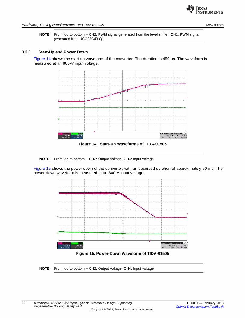
3.2.3 Start-Up and Power DownFigure 14 shows the start-up waveform of the converter. The duration is 450 µs. The waveform ismeasured at an 800-V input voltage.
Figure 14. Start-Up Waveforms of TIDA-01505
NOTE: From top to bottom – CH2: Output voltage, CH4: Input voltage
Figure 15 shows the power down of the converter, with an observed duration of approximately 50 ms. Thepower-down waveform is measured at an 800-V input voltage.
Figure 15. Power-Down Waveform of TIDA-01505
NOTE: From top to bottom – CH2: Output voltage, CH4: Input voltage

www.ti.com Hardware, Testing Requirements, and Test Results
21TIDUDT5–February 2018Submit Documentation Feedback
Copyright © 2018, Texas Instruments Incorporated
Automotive 40-V to 1-kV Input Flyback Reference Design SupportingRegenerative Braking Safety Test
3.2.4 Output Voltage RippleThe output voltage ripple of the design is measured under light-load- and full-load conditions, respectively.A 600-V input voltage is applied. Figure 16 and Figure 17 show the waveforms. Note how less than 50-mVpeak-to-peak ripple voltage is obtained at a 4-A full load.
Figure 16. Output Voltage Ripple of TIDA-01505 Under VIN = 600 V and 0.2-A Load (With Optocoupler)
Figure 17. Output Voltage Ripple of TIDA-01505 Under VIN = 600 V and IOUT = 4 A (With Optocoupler)

Hardware, Testing Requirements, and Test Results www.ti.com
22 TIDUDT5–February 2018Submit Documentation Feedback
Copyright © 2018, Texas Instruments Incorporated
Automotive 40-V to 1-kV Input Flyback Reference Design SupportingRegenerative Braking Safety Test
3.2.5 Switch Node WaveformsThe gate drive and the switch node voltage waveforms of the converter are measured under various inputvoltage and load conditions. Both of the design variants with and without optocoupler (PSR) are tested.
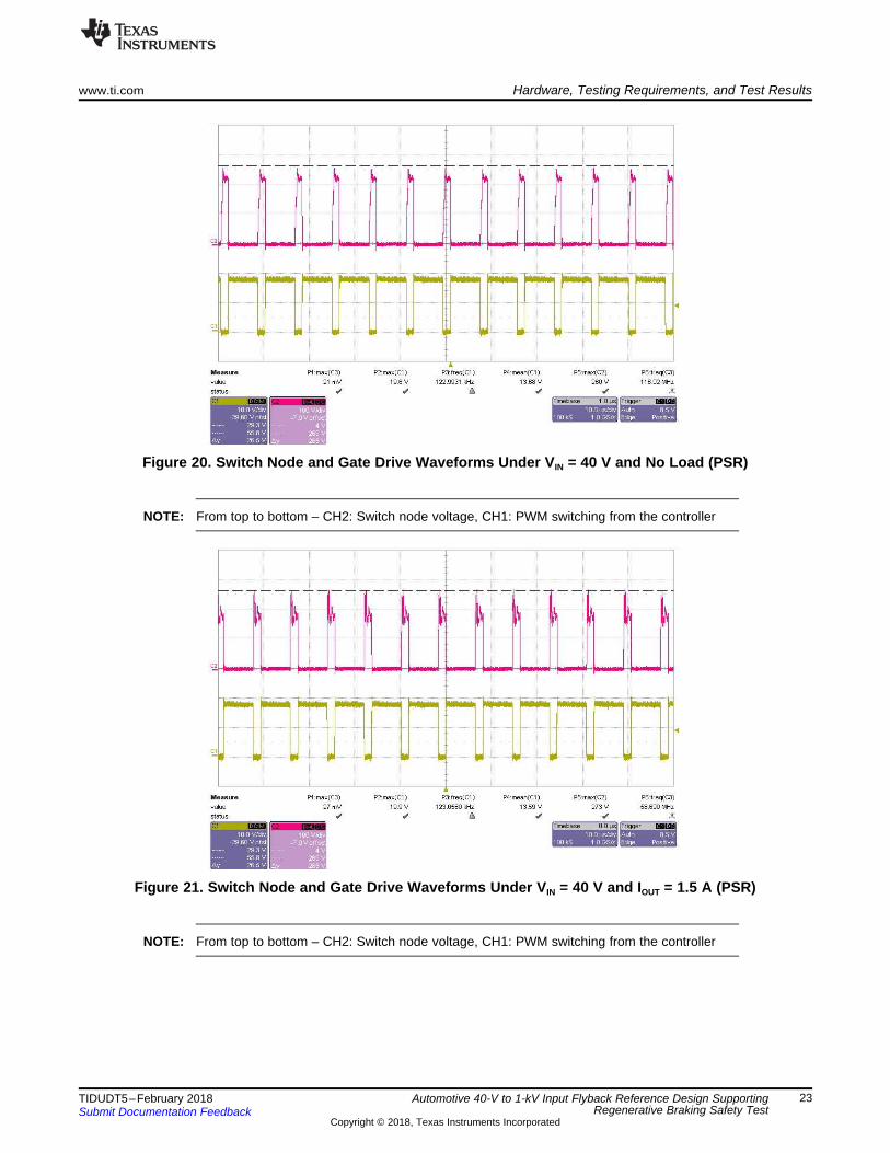
3.2.5.1 With 40-V InputFigure 18 through Figure 21 show the switch node and gate drive waveforms under the 40-V input.
Figure 18. Switch Node and Gate Drive Waveforms Under VIN = 40 V and No Load (With Optocoupler)
NOTE: From top to bottom – CH2: Switch node voltage, CH1: PWM switching from the controller
Figure 19. Switch Node and Gate Drive Waveforms Under VIN = 40 V, IOUT = 3 A (With Optocoupler)
NOTE: From top to bottom – CH2: Switch node voltage, CH1: PWM switching from the controller
www.ti.com Hardware, Testing Requirements, and Test Results
23TIDUDT5–February 2018Submit Documentation Feedback
Copyright © 2018, Texas Instruments Incorporated
Automotive 40-V to 1-kV Input Flyback Reference Design SupportingRegenerative Braking Safety Test
Figure 20. Switch Node and Gate Drive Waveforms Under VIN = 40 V and No Load (PSR)
NOTE: From top to bottom – CH2: Switch node voltage, CH1: PWM switching from the controller
Figure 21. Switch Node and Gate Drive Waveforms Under VIN = 40 V and IOUT = 1.5 A (PSR)
NOTE: From top to bottom – CH2: Switch node voltage, CH1: PWM switching from the controller
Hardware, Testing Requirements, and Test Results www.ti.com
24 TIDUDT5–February 2018Submit Documentation Feedback
Copyright © 2018, Texas Instruments Incorporated
Automotive 40-V to 1-kV Input Flyback Reference Design SupportingRegenerative Braking Safety Test
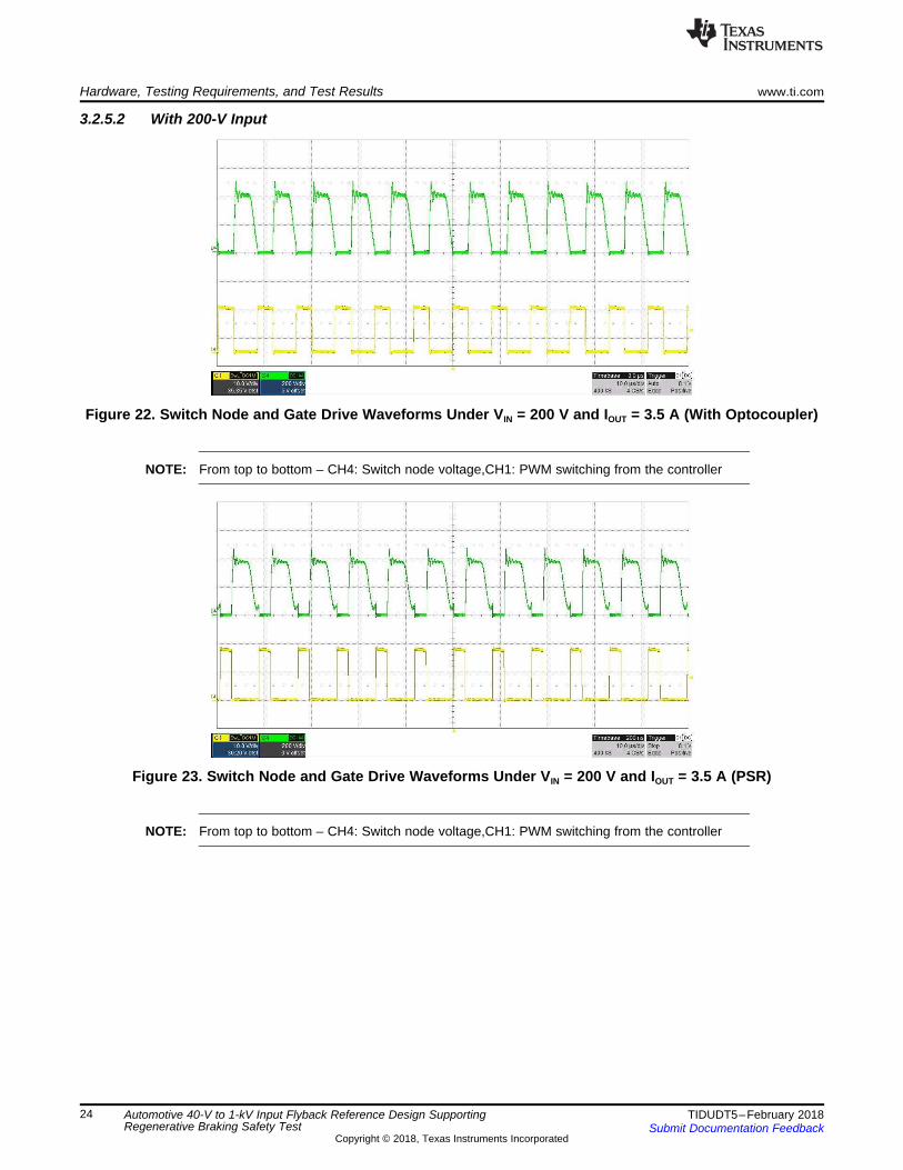
3.2.5.2 With 200-V Input
Figure 22. Switch Node and Gate Drive Waveforms Under VIN = 200 V and IOUT = 3.5 A (With Optocoupler)
NOTE: From top to bottom – CH4: Switch node voltage,CH1: PWM switching from the controller
Figure 23. Switch Node and Gate Drive Waveforms Under VIN = 200 V and IOUT = 3.5 A (PSR)
NOTE: From top to bottom – CH4: Switch node voltage,CH1: PWM switching from the controller

www.ti.com Hardware, Testing Requirements, and Test Results
25TIDUDT5–February 2018Submit Documentation Feedback
Copyright © 2018, Texas Instruments Incorporated
Automotive 40-V to 1-kV Input Flyback Reference Design SupportingRegenerative Braking Safety Test
3.2.5.3 With 400-V Input
Figure 24. Switch Node and Gate Drive Waveforms Under VIN = 400 V and IOUT = 4 A (With Optocoupler)
NOTE: From top to bottom – CH4: Switch node voltage, CH1: PWM switching from the controller
Figure 25. Switch Node and Gate Drive Waveforms Under VIN = 400 V and IOUT = 4 A (PSR)
NOTE: From top to bottom – CH4: Switch node voltage, CH1: PWM switching from the controller

Hardware, Testing Requirements, and Test Results www.ti.com
26 TIDUDT5–February 2018Submit Documentation Feedback
Copyright © 2018, Texas Instruments Incorporated
Automotive 40-V to 1-kV Input Flyback Reference Design SupportingRegenerative Braking Safety Test
3.2.5.4 Higher Than 400-V Input
Figure 26. Switch Node and Gate Drive Waveforms Under VIN = 600 V and IOUT = 4 A (With Optocoupler)
NOTE: From top to bottom – CH4: Switch node voltage, CH2: Output voltage ripple, CH1: PWMswitching from the controller
Figure 27. Switch Node and Gate Drive Waveforms Under VIN = 800 V and IOUT = 4 A (With Optocoupler)
NOTE: From top to bottom – CH4: Switch node voltage, CH1: PWM switching from the controller

Lab HVPower Supply
TIDA-01505
Electronic Load
Digital Multimeter (Output Voltage Measurement)
Digital Multimeter
(Input Voltage measurement)
Digital Multimeter
(Input Current Measurement)
Digital Multimeter
(Output Current Measurement)
Precision Shunt
1
2
3
5
4
6
7VBIAS1 = 20 V
VBIAS2 = ±5 V
UCC28C43-Q1
Gate
Vcc
Start-upCircuit
SiC
OptocouplerCOMP
VIN = 40 V to 1000 V
Optional
Level Shifter
VOUT
Voltage Divider
High Voltage +
High Voltage ±
TL431A-Q1
Copyright © 2018, Texas Instruments Incorporated
www.ti.com Hardware, Testing Requirements, and Test Results
27TIDUDT5–February 2018Submit Documentation Feedback
Copyright © 2018, Texas Instruments Incorporated
Automotive 40-V to 1-kV Input Flyback Reference Design SupportingRegenerative Braking Safety Test
Figure 28. Switch Node and Gate Drive Waveforms Under VIN = 1000 V and IOUT = 4 A (With Optocoupler)
NOTE: From top to bottom – CH4: Switch node voltage, CH1: PWM switching from the controller
The switch node waveform becomes flat at the top because the voltage probe is saturated.
3.2.6 EfficiencyThe efficiency of the design is measured under conditions of various input voltages. Figure 29 shows themeasurement setup. Two precision digital multimeters are placed at the input for measuring the inputvoltage and input current, respectively. The input voltage is measured through a resistive voltage divider.The input current is measured at the input ground terminal to avoid the high CM voltage stress. Anothermultimeter is placed at the output for measuring the output voltage. The output current is indirectlymeasured by the voltage drop from a precision shunt resistor.
Figure 29. Experiment Setup for Measuring Efficiency of TIDA-01505

Output Current (A)
Effi
cien
cy (
PS
R)
0.25 0.5 0.75 1 1.25 1.5 1.75 2 2.25 2.5 2.75 3 3.25 3.5 3.7510%
15%
20%
25%
30%
35%
40%
45%
50%
55%
60%
65%
70%
75%
80%
85%
90%
95%
100%
D001
VIN = 200 VVIN = 400 VVIN = 600 VVIN = 800 VVIN = 1000 V
Output Current (A)
Effi
cien
cy (
PS
R)
0.25 0.5 0.75 1 1.25 1.5 1.75 2 2.25 2.5 2.75 3 3.25 3.5 3.7510%
15%
20%
25%
30%
35%
40%
45%
50%
55%
60%
65%
70%
75%
80%
85%
90%
95%
100%
D004
VIN = 200 VVIN = 400 VVIN = 600 VVIN = 800 VVIN = 1000 V
Hardware, Testing Requirements, and Test Results www.ti.com
28 TIDUDT5–February 2018Submit Documentation Feedback
Copyright © 2018, Texas Instruments Incorporated
Automotive 40-V to 1-kV Input Flyback Reference Design SupportingRegenerative Braking Safety Test
Figure 30 shows the measured efficiency of the design with the optocoupler version. Note that the peakefficiency of 85% is achieved at a 400-V input voltage and 2-A load.
Figure 30. Measured Efficiency of Optocoupler Flyback in TIDA-01505
Figure 31 shows the measured efficiency of the design without the optocoupler version. Note that the peakefficiency of 86% is achieved at a 200-V input voltage and 1-A load.
Figure 31. Measured Efficiency of PSR Flyback in TIDA-01505

Output Current (A)
Out
put V
olta
ge w
ith O
ptoc
oupl
er (
V)
0.25 0.5 0.75 1 1.25 1.5 1.75 2 2.25 2.5 2.75 3 3.25 3.5 3.7515.7
15.71
15.72
15.73
15.74
15.75
15.76
15.77
15.78
15.79
15.8
15.81
15.82
15.83
D003
VIN = 200 VVIN = 400 VVIN = 600 VVIN = 800 VVIN = 1000 V
Output Current (A)
Out
put V
olta
ge (
V)
0.25 0.5 0.75 1 1.25 1.5 1.75 2 2.25 2.5 2.75 3 3.25 3.5 3.759.5
10
10.5
11
11.5
12
12.5
13
13.5
14
14.5
15
15.5
D002
VIN = 200 VVIN = 400 VVIN = 600 VVIN = 800 VVIN = 1000 V
www.ti.com Hardware, Testing Requirements, and Test Results
29TIDUDT5–February 2018Submit Documentation Feedback
Copyright © 2018, Texas Instruments Incorporated
Automotive 40-V to 1-kV Input Flyback Reference Design SupportingRegenerative Braking Safety Test
3.2.7 Load RegulationLoad regulation measurements show the % deviation from the nominal output voltage as a function ofoutput current. The experiment setup is the same as that of the efficiency measurement (see Figure 29).Figure 32 and Figure 33 show the measured results of the PSR flyback and optocoupler flyback variants,respectively.
Figure 32. Load Regulation of PSR Flyback in TIDA-01505
Figure 33. Load Regulation of Flyback With Optocoupler in TIDA-01505

Hardware, Testing Requirements, and Test Results www.ti.com
30 TIDUDT5–February 2018Submit Documentation Feedback
Copyright © 2018, Texas Instruments Incorporated
Automotive 40-V to 1-kV Input Flyback Reference Design SupportingRegenerative Braking Safety Test
3.2.8 Control Loop Frequency ResponseThe control loop frequency response represents the stability of the power supply system. The loopfrequency response of the design is measured under various loads and input voltages, respectively. Theworst condition occurs when the converter runs under the minimum input voltage and a full load.
3.2.8.1 PSR FlybackThis subsection shows the control loop response of the design version without an optocoupler. Figure 34shows the plot when the input is 40 V and the load is 100 mA. Note that a 100° phase margin is achieved.
Figure 34. Loop Frequency Response With VIN = 40 V and 0.10A Load (Without Optocoupler)
Figure 35 shows the plot when the input is 40 V at a 1.5-A load. Note that a 94° phase margin isachieved.
Figure 35. Loop Frequency Response With VIN = 40 V and 1.5-A Load (Without Optocoupler)

www.ti.com Hardware, Testing Requirements, and Test Results
31TIDUDT5–February 2018Submit Documentation Feedback
Copyright © 2018, Texas Instruments Incorporated
Automotive 40-V to 1-kV Input Flyback Reference Design SupportingRegenerative Braking Safety Test
Figure 36 shows the plot when the input is 120 V at a 0.1-A load. Note that a 84° phase margin isachieved.
Figure 36. Loop Frequency Response With VIN = 120 V and 0.1-A Load (Without Optocoupler)
Figure 37 shows the plot when the input is 120 V at a 2-A load. Note that a 94° phase margin is achieved.
Figure 37. Loop Frequency Response With VIN = 120 V and 2-A Load (Without Optocoupler)

Hardware, Testing Requirements, and Test Results www.ti.com
32 TIDUDT5–February 2018Submit Documentation Feedback
Copyright © 2018, Texas Instruments Incorporated
Automotive 40-V to 1-kV Input Flyback Reference Design SupportingRegenerative Braking Safety Test
3.2.8.2 Flyback With OptocouplerThis subsection shows the control loop response of the design version with an optocoupler. Figure 38shows the plot when the input is 40 V at a 0.1-A load. Note that a 82° phase margin is achieved.
Figure 38. Loop Frequency Response With VIN = 40 V and 0.1-A Load (With Optocoupler)
Figure 39 shows the plot when the input is 40 V at a 2.7-A load. Note that a 77° phase margin isachieved.
Figure 39. Loop Frequency Response With VIN = 40 V and 2.7-A Load (With Optocoupler)

www.ti.com Hardware, Testing Requirements, and Test Results
33TIDUDT5–February 2018Submit Documentation Feedback
Copyright © 2018, Texas Instruments Incorporated
Automotive 40-V to 1-kV Input Flyback Reference Design SupportingRegenerative Braking Safety Test
Figure 40 shows the plot when the input is 120 V at a 0.1-A load. Note that a 89° phase margin isachieved.
Figure 40. Loop Frequency Response With VIN = 120 V and 0.1-A Load (With Optocoupler)
Figure 41 shows the plot when the input is 120 V at a 4-A load. Note that a 82° phase margin is achieved.
Figure 41. Loop Frequency Response With VIN = 120 V and 4-A Load (With Optocoupler)

Hardware, Testing Requirements, and Test Results www.ti.com
34 TIDUDT5–February 2018Submit Documentation Feedback
Copyright © 2018, Texas Instruments Incorporated
Automotive 40-V to 1-kV Input Flyback Reference Design SupportingRegenerative Braking Safety Test
3.2.9 Load Transient ResponseA load transient response presents how well a power supply copes with the changes in the load currentdemand. Figure 42 and Figure 43 show the load transient response of two converter variants in thereference design, respectively. A 800-V input voltage is applied. The load is switching from 1 A to 4 A witha period of 100 ms and a 50% duty cycle.
Figure 42. Load Transient Response of Flyback With Optocoupler Under VIN = 800 V and IOUT SwitchingBetween 1 A and 4 A
NOTE: (From top to bottom – CH2: Output voltage ripple, CH3: Load current)
Figure 43 shows the load transient response of the PSR Flyback converter when the input voltage is800 V. The load is switching from 1 A to 4 A with a period of 100 ms and a 50% duty cycle.
Figure 43. Load Transient Response of PSR Flyback Under VIN = 800 V and IOUT SwitchingBetween 1 A and 4 A
NOTE: (From top to bottom – CH2: Output voltage ripple, CH3: Load current)

Transformer
SiC MOSFET
D25
Transformer
www.ti.com Hardware, Testing Requirements, and Test Results
35TIDUDT5–February 2018Submit Documentation Feedback
Copyright © 2018, Texas Instruments Incorporated
Automotive 40-V to 1-kV Input Flyback Reference Design SupportingRegenerative Braking Safety Test
3.2.10 Thermal ImagesThe thermal image of the design board is measured under a 600-V input voltage and full-load conditions.The circuit runs at the room temperature for 15 minutes. The converter is loaded with 4 A and the outputpower is 60 W. Figure 44 shows the temperature of the transformer surface, PCB traces, heat sink of thesecondary diode (D25), and the SiC MOSFET. The transformer area appears to have the highesttemperature. The PCB traces, which are located next to the transformer, also appear to retain heat. Thediode at the output and the SiC MOSFET are kept under cool temperature.
Figure 44. Thermal Image of Board Top Side
NOTE: Measured at VIN = 600 V, POUT = 60 W running for 20 minutes at room temperature
Figure 45 shows the temperature of the transformer winding. The peak temperature of the transformerwinding reaches 113.4°C.
Figure 45. Thermal Image of Power Transformer
NOTE: Measured at VIN = 600 V, POUT = 60 W running for 20 minutes at room temperature

TL431A-Q1UCC28C43-Q1
Hardware, Testing Requirements, and Test Results www.ti.com
36 TIDUDT5–February 2018Submit Documentation Feedback
Copyright © 2018, Texas Instruments Incorporated
Automotive 40-V to 1-kV Input Flyback Reference Design SupportingRegenerative Braking Safety Test
Figure 46 shows the temperature of the device ICs. The peak temperature is kept below 40°C.
Figure 46. Thermal Image of Device ICs UCC28C43-Q1 and TL431A-Q1
NOTE: Measured at VIN = 600 V, POUT = 60 W running for 20 minutes at room temperature

C5 T1
SiC MOSFET
Current Sense Resistor
R31 R32
www.ti.com Design Files
37TIDUDT5–February 2018Submit Documentation Feedback
Copyright © 2018, Texas Instruments Incorporated
Automotive 40-V to 1-kV Input Flyback Reference Design SupportingRegenerative Braking Safety Test
4 Design Files
4.1 SchematicsTo download the schematics, see the design files at TIDA-01505.
4.2 Bill of MaterialsTo download the bill of materials (BOM), see the design files at TIDA-01505.
4.3 PCB Layout Recommendations
4.3.1 Layout PrintsTo download the layer plots, see the design files at TIDA-01505.
4.3.2 Layout GuidelinesThis reference design implements a two-layer PCB. Figure 47 shows the board material, copper thickness,and the dielectric distance in between.
Figure 47. Layer Stack of TIDA-01505
Figure 48 shows the component placement for the main current-flowing loop. The input film capacitor, SiCMOSFET, and current sense resistors are placed as close as possible to the transformer T1 to minimizethe loop.
Figure 48. Component Placement of Main Current Flowing Loop

High-Ohmic Resistive Chain
Low-Ohmic Resistive Chain
High-Voltage Bipolar Transistor
SiC MOSFET
UCC28C43-Q1
Current Sense Resistor R31 R32
Gate Resistors
Design Files www.ti.com
38 TIDUDT5–February 2018Submit Documentation Feedback
Copyright © 2018, Texas Instruments Incorporated
Automotive 40-V to 1-kV Input Flyback Reference Design SupportingRegenerative Braking Safety Test
Figure 49 shows the component placement of the gate drive loop, which includes the storage capacitorC28, UCC28C43-Q1, gate resistors, SiC MOSFET, and current sense resistors. The PCB traces forcurrent sensing are kept close and identical to minimize the differential noise crosstalks.
Figure 49. Component Placement of Gate Drive Loop
Figure 50 shows the component placement of the active start-up circuit. This circuit consists of the high-ohmic- and low-ohmic resistive lanes, and the two lanes are placed in parallel connecting the high-voltageside to the low-voltage side.
Figure 50. Component Placement of Active Start-Up Circuit

Compensation Network
Decoupling Capacitors
UCC28C43-Q1
RC filter for the current sense
Snubber Network
www.ti.com Design Files
39TIDUDT5–February 2018Submit Documentation Feedback
Copyright © 2018, Texas Instruments Incorporated
Automotive 40-V to 1-kV Input Flyback Reference Design SupportingRegenerative Braking Safety Test
Figure 51 shows the component placement of the snubber network. This network is connected closebetween the transformer output and DC bus+ to minimize the current-flowing loop.
Figure 51. Component Placement of Snubber Network
Figure 52 shows the placement of components surrounding the UCC28C43-Q1 controller. Thecomponents are placed as close as possible to the IC to avoid any noise coupling. For more guidelines,see the section regarding layout guidelines in the UCC28C43-Q1 data sheet: UCC28C4x-Q1 AutomotiveBiCMOS Low-Power Current-Mode PWM Controllers.
Figure 52. Component Placement Surrounding UCC28C43-Q1 Controller
4.4 Altium ProjectTo download the Altium project files, see the design files at
To download the bill of materials (BOM), see the design files at TIDA-01505..
4.5 Gerber FilesTo download the Gerber files, see the design files at
To download the bill of materials (BOM), see the design files at TIDA-01505..
4.6 Assembly DrawingsTo download the assembly drawings, see the design files at
To download the bill of materials (BOM), see the design files at TIDA-01505..

Related Documentation www.ti.com
40 TIDUDT5–February 2018Submit Documentation Feedback
Copyright © 2018, Texas Instruments Incorporated
Automotive 40-V to 1-kV Input Flyback Reference Design SupportingRegenerative Braking Safety Test
5 Related Documentation
1. Texas Instruments, Automotive Wide VIN Front-End Power Reference Design With Cold CrankOperation and Transient Protections
2. Texas Instruments, MODELING, ANALYSIS AND COMPENSATION OF THE CURRENT-MODECONVERTER
3. Texas Instruments, PRACTICAL CONSIDERATIONS IN CURRENT MODE POWER SUPPLIES
5.1 TrademarksE2E is a trademark of Texas Instruments.All other trademarks are the property of their respective owners.
6 TerminologyAEC— Automotive Electronics Council
AFE— Analog front end
BOM— Bill of materials
CISPR— International Special Committee on Radio Interference
CM— Common mode
CCM— Continuous conduction mode
DCM— Discontinuous conduction mode
DM— Differential mode
EMC— Electromagnetic compatibility
EMI— Electromagnetic interference
ESR— Equivalent series resistance
EV— Electric vehicle
HEV— Hybrid electric vehicle
MOSFET— Metal-oxide-semiconductor field-effect transistor
OEM— Original equipment manufacturer
PCB— Printed-circuit board
PE— Protective earth
PSR— Primary side regulation
RMS— Root mean square
UVLO— Undervoltage lockout
7 About the AuthorXUN GONG is an Automotive Systems Engineer at Texas Instruments, where he is responsible fordeveloping reference design solutions for the automotive segment in HEV/EV Power Train applications.Xun brings to this role expertise in the field of IGBT and SiC (Silicon Carbide) power transistors, Motordrive applications, non-isolated and isolated DC-DC converters up t 6.6 kilowatt. Xun achieved his Ph.D.in Electrical Engineering from Delft University of Technology in Delft, Netherlands. Xun Gong won the 1stprize papers of the Academic Journal IEEE Transactions on Power Electronics of 2014.

IMPORTANT NOTICE FOR TI DESIGN INFORMATION AND RESOURCES
Texas Instruments Incorporated (‘TI”) technical, application or other design advice, services or information, including, but not limited to,reference designs and materials relating to evaluation modules, (collectively, “TI Resources”) are intended to assist designers who aredeveloping applications that incorporate TI products; by downloading, accessing or using any particular TI Resource in any way, you(individually or, if you are acting on behalf of a company, your company) agree to use it solely for this purpose and subject to the terms ofthis Notice.TI’s provision of TI Resources does not expand or otherwise alter TI’s applicable published warranties or warranty disclaimers for TIproducts, and no additional obligations or liabilities arise from TI providing such TI Resources. TI reserves the right to make corrections,enhancements, improvements and other changes to its TI Resources.You understand and agree that you remain responsible for using your independent analysis, evaluation and judgment in designing yourapplications and that you have full and exclusive responsibility to assure the safety of your applications and compliance of your applications(and of all TI products used in or for your applications) with all applicable regulations, laws and other applicable requirements. Yourepresent that, with respect to your applications, you have all the necessary expertise to create and implement safeguards that (1)anticipate dangerous consequences of failures, (2) monitor failures and their consequences, and (3) lessen the likelihood of failures thatmight cause harm and take appropriate actions. You agree that prior to using or distributing any applications that include TI products, youwill thoroughly test such applications and the functionality of such TI products as used in such applications. TI has not conducted anytesting other than that specifically described in the published documentation for a particular TI Resource.You are authorized to use, copy and modify any individual TI Resource only in connection with the development of applications that includethe TI product(s) identified in such TI Resource. NO OTHER LICENSE, EXPRESS OR IMPLIED, BY ESTOPPEL OR OTHERWISE TOANY OTHER TI INTELLECTUAL PROPERTY RIGHT, AND NO LICENSE TO ANY TECHNOLOGY OR INTELLECTUAL PROPERTYRIGHT OF TI OR ANY THIRD PARTY IS GRANTED HEREIN, including but not limited to any patent right, copyright, mask work right, orother intellectual property right relating to any combination, machine, or process in which TI products or services are used. Informationregarding or referencing third-party products or services does not constitute a license to use such products or services, or a warranty orendorsement thereof. Use of TI Resources may require a license from a third party under the patents or other intellectual property of thethird party, or a license from TI under the patents or other intellectual property of TI.TI RESOURCES ARE PROVIDED “AS IS” AND WITH ALL FAULTS. TI DISCLAIMS ALL OTHER WARRANTIES ORREPRESENTATIONS, EXPRESS OR IMPLIED, REGARDING TI RESOURCES OR USE THEREOF, INCLUDING BUT NOT LIMITED TOACCURACY OR COMPLETENESS, TITLE, ANY EPIDEMIC FAILURE WARRANTY AND ANY IMPLIED WARRANTIES OFMERCHANTABILITY, FITNESS FOR A PARTICULAR PURPOSE, AND NON-INFRINGEMENT OF ANY THIRD PARTY INTELLECTUALPROPERTY RIGHTS.TI SHALL NOT BE LIABLE FOR AND SHALL NOT DEFEND OR INDEMNIFY YOU AGAINST ANY CLAIM, INCLUDING BUT NOTLIMITED TO ANY INFRINGEMENT CLAIM THAT RELATES TO OR IS BASED ON ANY COMBINATION OF PRODUCTS EVEN IFDESCRIBED IN TI RESOURCES OR OTHERWISE. IN NO EVENT SHALL TI BE LIABLE FOR ANY ACTUAL, DIRECT, SPECIAL,COLLATERAL, INDIRECT, PUNITIVE, INCIDENTAL, CONSEQUENTIAL OR EXEMPLARY DAMAGES IN CONNECTION WITH ORARISING OUT OF TI RESOURCES OR USE THEREOF, AND REGARDLESS OF WHETHER TI HAS BEEN ADVISED OF THEPOSSIBILITY OF SUCH DAMAGES.You agree to fully indemnify TI and its representatives against any damages, costs, losses, and/or liabilities arising out of your non-compliance with the terms and provisions of this Notice.This Notice applies to TI Resources. Additional terms apply to the use and purchase of certain types of materials, TI products and services.These include; without limitation, TI’s standard terms for semiconductor products http://www.ti.com/sc/docs/stdterms.htm), evaluationmodules, and samples (http://www.ti.com/sc/docs/sampterms.htm).
Mailing Address: Texas Instruments, Post Office Box 655303, Dallas, Texas 75265Copyright © 2018, Texas Instruments Incorporated