Audio power amplifiers - narod.rukkbweb.narod.ru/spravochnik/datasheet/philips_amps.pdfAudio...
55
Audio power amplifiers Audio Power Designer’s guide - October 1996
Transcript of Audio power amplifiers - narod.rukkbweb.narod.ru/spravochnik/datasheet/philips_amps.pdfAudio...

Audio poweramplifiers
Audio Power
Designer’s guide - October 1996
11687 Cover COmpact 24/9/97 10:20 AM Page 1

1
Audio Amplifier ICs
AUDIO AMPLIFIER ICS DESIGNER’S GUIDE
Contents
Section Page
1 Introduction . . . . . . . . . . . . . . . . . . . . . . . . . . . . . . . . . . . . . . . . . . . . . . . . . . . . . . . . . . . . . . . . . . . . 1-2
2 Product survey and page reference . . . . . . . . . . . . . . . . . . . . . . . . . . . . . . . . . . . . . . . . . . . . . . . . . . 2-1
In application sequence . . . . . . . . . . . . . . . . . . . . . . . . . . . . . . . . . . . . . . . . . . . . . . . . . . . . . . . . 2-2
In power output sequence . . . . . . . . . . . . . . . . . . . . . . . . . . . . . . . . . . . . . . . . . . . . . . . . . . . . . 2-5
3 Audio amplifier ICs for portable radio/audio equipment . . . . . . . . . . . . . . . . . . . . . . . . . . . . . . . . . 3-1
4 Audio amplifier ICs for car radios/power boosters . . . . . . . . . . . . . . . . . . . . . . . . . . . . . . . . . . . . . 4-1
5 Audio amplifier ICs for mains-powered systems including hi-fi and TV sound . . . . . . . . . . . . . . . . 5-1
Appendices
1 Further information . . . . . . . . . . . . . . . . . . . . . . . . . . . . . . . . . . . . . . . . . . . . . . . . . . . . . . . . . . . . . A-2
Data . . . . . . . . . . . . . . . . . . . . . . . . . . . . . . . . . . . . . . . . . . . . . . . . . . . . . . . . . . . . . . . . . . . . . . A-2
Application notes and leaflet . . . . . . . . . . . . . . . . . . . . . . . . . . . . . . . . . . . . . . . . . . . . . . . . . . . A-2
2 Index of audio amplifier ICs . . . . . . . . . . . . . . . . . . . . . . . . . . . . . . . . . . . . . . . . . . . . . . . . . . . . . . . A-3
1-1
NOTEPurchase of Philips I2C components conveys a license under the Philips I2Cpatent to use the components in the I2Csystem, provided the system conforms tothe I2C specifications defined by Philips.

Audio Amplifier ICs
INTRODUCTION
1-2
1Few people realize that one of the world’s first ICs was an audiopower amplifier from Philips. This delivered a mere 25 mW intoa hearing-aid earpiece and incorporated just three transistors and2 resistors.
Not surprisingly, we’ve made many advances since that initialintroduction. Advances that have led to ICs such as theTDA8551 incorporating digital volume control with a controlrange of more than 80 dB. Or the hi-fi TDA1514A, which candeliver 50 W – more than two thousand times the power of thatfirst integrated amplifier.
These are just two of the extensive range of audio ICs we nowsupply for a whole host of applications – including portableradio and recorders, car radios, multimedia systems, hi-fi TV,radio and music centres, and digital audio systems.
Integrated powerA major feature of our latest range is the high degree of func-tional power integrated within each package. A functional powerthat dramatically reduces the peripheral component count offinished equipment, leading to:• lower system development costs • smaller, more compact circuitry• far fewer production problems • significantly lower production costs.
What’s more, advanced internal protection circuitry completelyeliminates danger of damage from thermal runaway, short-circuits and electrostatic discharge. Providing a level of circuitreliability formerly the exclusive preserve of professional systems,and, moreover, providing you with a solid guarantee of qualityand reliability in your own systems.
A valuable aid to designersIn the following pages you’ll find our complete range of audioamplifiers. Intended principally as a designer’s first selectionguide, the pages give the most important parameters, or at least,those that feature prominently when design criteria are initiallybeing considered. Used in conjunction with our DataHandbook IC01 (which gives more detailed information), thisguide provides audio system designers with a ready means ofselecting the most appropriate components for their designs.
The publication is divided into three application areas: portableradio/audio, car radio and mains-powered systems. Many prod-ucts, however, may be suitable for several application areas: caraudio systems and mains-powered multimedia PCs for example.What’s more, many of today’s applications for audio amplifierICs, e.g. musical greeting cards, were unheard of just a few yearsago. This means that any subdivision such as that given in thisguide can be only a preliminary indication of a product’s suit-ability for a particular application. In using this guide, therefore,designers should cast their net as wide as possible and shouldconsider all likely candidates when looking for a suitable audioIC for their application.
INTEGRATED POWER WITH PHILIPS AUDIO AMPLIFIER ICs

2
Audio Amplifier ICs
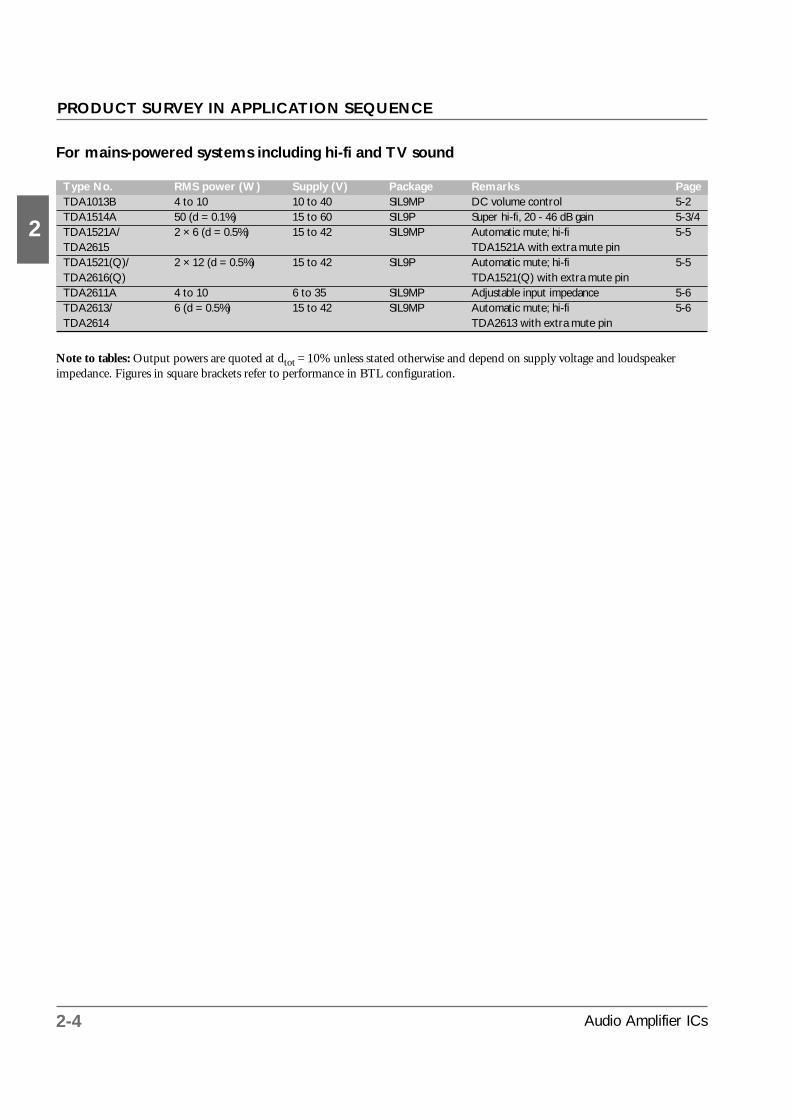
PRODUCT SURVEY IN APPLICATION SEQUENCE
2-1
PRODUCT SURVEYPRODUCT SURVEY

2
Audio Amplifier ICs2-2
For portable radio/audio equipment
Type No. RMS power (W) Supply (V) Package Remarks PageTDA1011 6.5 3.6 to 24 SIL9MP Separate pre/power amplifiers 3-2TDA1015 4 3.6 to 18 SIL9MP Separate pre/power amplifiers 3-2TDA1015T 0.5 3.6 to 12 SO8 Separate pre/power amplifiers 3-2TDA1016 2 3.6 to 15 DIP16 Record/playback + ALC 3-3TDA1308T 2 × 0.06 (d = 0.1%) 3 to 7 SO8 Stereo headphone driver 3-4TDA7050(T) [0.15]/2 × 0.075 1.6 to 6 DIP8, SO8 No peripheral components 3-5TDA7052/ 1 3 to 18 DIP8 No peripheral components 3-6TDA7053 2 × 1 No peripheral componentsTDA7052A(AT)/ 1(0.5) 4.5 to 18 DIP8, SO8 DC volume control; 36 dB gain 3-7TDA7052B(BT) TDA7052A(AT) with 40 dB gainTDA7053A(AT) 2 × 1(2 × 0.5) 4.5 to 18 DIP16, SO16 DC volume control; 40 dB gain 3-8TDA7056/ 3 3 to 18 SIL9MP No peripheral components 3-9TDA7057Q 2 × 3 SIL13P No peripheral componentsTDA7056A/ 5 4.5 to 18 SIL9MP DC volume control; 36 dB gain 3-10TDA7056B TDA7056A with 40 dB gainTDA7057AQ 2 × 5 4.5 to 18 SIL13P DC volume control; 40 dB gain 3-11TDA8541(T) 1 2.2 to 18 DIP8, SO8 Few peripheral components 3-12TDA8542(T) 2 × 1 2.2 to 18 DIP16, SO16L Few peripheral components 3-13TDA8543(T) 2 2.2 to 18 DIP16, SO16 Few peripheral components 3-14TDA8547(T) 2 × 1 2.2 to 18 DIP16, SO16L Standby per channel 3-15TDA8551(T) 1 2.7 to 6 DIP8, SO8 Digital volume control 3-16TDA8558(T) 0.125 1.8 to 18 DIP8, SO8 Power saving muting facility 3-17TDA8559(T) 0.035 1.8 to 30 DIP16, SO16 Stereo headphone amplifier 3-18
Note to tables: Output powers are quoted at dtot = 10% unless stated otherwise and depend on supply voltage and loudspeakerimpedance. Figures in square brackets refer to performance in BTL configuration.
PRODUCT SURVEY IN APPLICATION SEQUENCE

2-3Audio Amplifier ICs
2
For car radios/power boosters
Type No. RMS power (W) Supply (V) Package Remarks PageTDA1010A/ 3.4 to 12 6 to 24 SIL9MP Separate pre/power amplifiers 4-2TDA1020 + load dump prot., standby, HF limitTDA1510AQ/ 2 × 12[1 × 24] 6 to 18 SIL13P 1-end/BTL, 26 - 50[32 - 56] dB gain 4-3TDA1515BQ TDA1510AQ with LS protectionTDA1516BQ/ 2 × 12[1 × 24] 8.5 to 18 SIL13P 2 × 1-end/1 × BTL, 20[26] dB gain 4-4TDA1516CQ/ TDA1516BQ but BTL onlyTDA1518BQ TDA1516BQ with 40[46] dB gainTDA1517(P)/ 2 × 6 8.5 to 18 SIL9MP, DIP18 20 dB gain 4-5TDA1519 TDA1517 with 40 dB gainTDA1519A/ 2 × 11[1 × 22] 8.5 to 17.5 SIL9P 2 × 1-end/1 × BTL, 40[46] dB gain 4-6TDA1519B 2 × 6[1 × 12] 8.5 to 18 SIL9MPTDA1552Q/ [2 × 22] 8.5 to 18 SIL13P Dual BTL amplifiers, [26] dB gain 4-7TDA1553Q/ TDA1552Q with LS protectionTDA1553CQ/ TDA1553Q with CMOS mode switchTDA1557Q TDA1553Q with [46] dB gainTDA1554Q/ 4 × 11[2 × 22] 8.5 to 18 SIL17P 1-end/BTL, 20[26] dB gain 4-8TDA1555Q/ TDA1554Q with distortion detectorTDA1558Q TDA1554Q with 40[46] dB gainTDA1556Q [2 × 22] 8.5 to 18 SIL17P Dual BTL, diff. inputs, [26] dB gain 4-9TDA1560Q [40] 8 to 18 SIL17P BTL class-H amplifier, [30] dB gain 4-10TDA1561Q 2 × 23 6 to 18 DBS13P Automatic switching to high-power 4-11
mode when neededTDA8560Q/ [2 × 40] 8.5 to 18 SIL13P Dual BTL amplifiers. [40] dB gain 4-12TDA8563Q/ TDA8560Q with [26] dB gainTDA8563AQ TDA8563Q with 2.2% THD
(10% with TDA8563Q)TDA8561Q/ 4 × 12[2 × 24] 8.5 to 18 SIL17P 4 × 1-end/dual BTL, 20[26] dB gain 4-13TDA8564Q TDA8561Q with 40[46] dB gainTDA8562Q/ 4 × 12 8.5 to 18 SIL17P 4 × 1-end amplifier, 20 dB gain 4-14TDA8565Q TDA8562Q with 40 dB gainTDA8566Q 2 × 25 8.5 to 18 DBS17P Differential inputs 4-15TDA8567Q/ 4 × 25 8.5 to 18 DBS23P Quad BTL amplifier, 4 Ω load, [26] dB gain 4-16TDA8568Q/ TDA8567Q with [40] dB gainTDA8569Q TDA8567Q driving 2 Ω loadTDA8574(T) dual line driver 6 to 12 DIP16, SO16 Class H high output level 4-17TDA8576T dual line driver 6 to 12 SO16 Class H high output level 4-18TDA8577/ dual line driver 5 to 18 SIL9MP Completely separated inputs 4-19TDA8578(T)/ DIP16, SO16 Completely separated inputsTDA8579(T) DIP8, SO8 Inverting inputs linked
Note to tables: Output powers are quoted at dtot = 10% unless stated otherwise and depend on supply voltage and loudspeakerimpedance. Figures in square brackets refer to performance in BTL configuration.
PRODUCT SURVEY IN APPLICATION SEQUENCE
2-4
2
Audio Amplifier ICs
PRODUCT SURVEY IN APPLICATION SEQUENCE
For mains-powered systems including hi-fi and TV sound
Type No. RMS power (W) Supply (V) Package Remarks PageTDA1013B 4 to 10 10 to 40 SIL9MP DC volume control 5-2TDA1514A 50 (d = 0.1%) 15 to 60 SIL9P Super hi-fi, 20 - 46 dB gain 5-3/4TDA1521A/ 2 × 6 (d = 0.5%) 15 to 42 SIL9MP Automatic mute; hi-fi 5-5TDA2615 TDA1521A with extra mute pinTDA1521(Q)/ 2 × 12 (d = 0.5%) 15 to 42 SIL9P Automatic mute; hi-fi 5-5TDA2616(Q) TDA1521(Q) with extra mute pinTDA2611A 4 to 10 6 to 35 SIL9MP Adjustable input impedance 5-6TDA2613/ 6 (d = 0.5%) 15 to 42 SIL9MP Automatic mute; hi-fi 5-6TDA2614 TDA2613 with extra mute pin
Note to tables: Output powers are quoted at dtot = 10% unless stated otherwise and depend on supply voltage and loudspeakerimpedance. Figures in square brackets refer to performance in BTL configuration.
2-5Audio Amplifier ICs
2
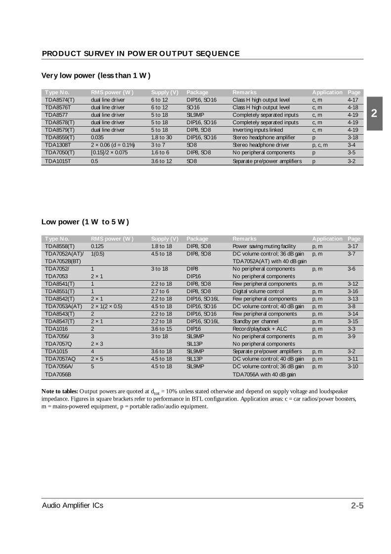
Very low power (less than 1 W)
Type No. RMS power (W) Supply (V) Package Remarks Application PageTDA8574(T) dual line driver 6 to 12 DIP16, SO16 Class H high output level c, m 4-17TDA8576T dual line driver 6 to 12 SO16 Class H high output level c, m 4-18TDA8577 dual line driver 5 to 18 SIL9MP Completely separated inputs c, m 4-19TDA8578(T) dual line driver 5 to 18 DIP16, SO16 Completely separated inputs c, m 4-19TDA8579(T) dual line driver 5 to 18 DIP8, SO8 Inverting inputs linked c, m 4-19TDA8559(T) 0.035 1.8 to 30 DIP16, SO16 Stereo headphone amplifier p 3-18TDA1308T 2 × 0.06 (d = 0.1%) 3 to 7 SO8 Stereo headphone driver p, c, m 3-4TDA7050(T) [0.15]/2 × 0.075 1.6 to 6 DIP8, SO8 No peripheral components p 3-5
TDA1015T 0.5 3.6 to 12 SO8 Separate pre/power amplifiers p 3-2
Low power (1 W to 5 W)
Type No. RMS power (W) Supply (V) Package Remarks Application PageTDA8558(T) 0.125 1.8 to 18 DIP8, SO8 Power saving muting facility p, m 3-17TDA7052A(AT)/ 1(0.5) 4.5 to 18 DIP8, SO8 DC volume control; 36 dB gain p, m 3-7TDA7052B(BT) TDA7052A(AT) with 40 dB gainTDA7052/ 1 3 to 18 DIP8 No peripheral components p, m 3-6TDA7053 2 × 1 DIP16 No peripheral componentsTDA8541(T) 1 2.2 to 18 DIP8, SO8 Few peripheral components p, m 3-12TDA8551(T) 1 2.7 to 6 DIP8, SO8 Digital volume control p, m 3-16TDA8542(T) 2 × 1 2.2 to 18 DIP16, SO16L Few peripheral components p, m 3-13TDA7053A(AT) 2 × 1(2 × 0.5) 4.5 to 18 DIP16, SO16 DC volume control; 40 dB gain p, m 3-8TDA8543(T) 2 2.2 to 18 DIP16, SO16 Few peripheral components p, m 3-14TDA8547(T) 2 × 1 2.2 to 18 DIP16, SO16L Standby per channel p, m 3-15TDA1016 2 3.6 to 15 DIP16 Record/playback + ALC p, m 3-3TDA7056/ 3 3 to 18 SIL9MP No peripheral components p, m 3-9TDA7057Q 2 × 3 SIL13P No peripheral componentsTDA1015 4 3.6 to 18 SIL9MP Separate pre/power amplifiers p, m 3-2TDA7057AQ 2 × 5 4.5 to 18 SIL13P DC volume control; 40 dB gain p, m 3-11TDA7056A/ 5 4.5 to 18 SIL9MP DC volume control; 36 dB gain p, m 3-10TDA7056B TDA7056A with 40 dB gain
Note to tables: Output powers are quoted at dtot = 10% unless stated otherwise and depend on supply voltage and loudspeakerimpedance. Figures in square brackets refer to performance in BTL configuration. Application areas: c = car radios/power boosters, m = mains-powered equipment, p = portable radio/audio equipment.
PRODUCT SURVEY IN POWER OUTPUT SEQUENCE
2-6
2
Audio Amplifier ICs
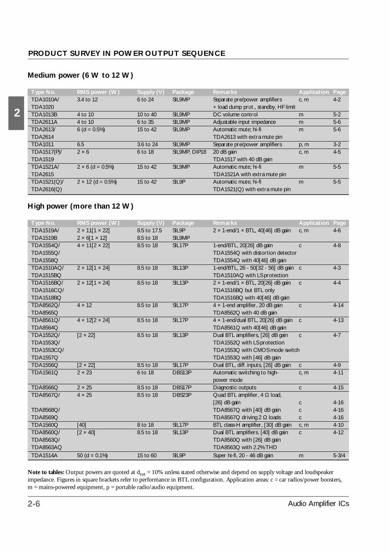
Medium power (6 W to 12 W)
Type No. RMS power (W) Supply (V) Package Remarks Application PageTDA1010A/ 3.4 to 12 6 to 24 SIL9MP Separate pre/power amplifiers c, m 4-2TDA1020 + load dump prot., standby, HF limitTDA1013B 4 to 10 10 to 40 SIL9MP DC volume control m 5-2TDA2611A 4 to 10 6 to 35 SIL9MP Adjustable input impedance m 5-6TDA2613/ 6 (d = 0.5%) 15 to 42 SIL9MP Automatic mute; hi-fi m 5-6TDA2614 TDA2613 with extra mute pinTDA1011 6.5 3.6 to 24 SIL9MP Separate pre/power amplifiers p, m 3-2TDA1517(P)/ 2 × 6 6 to 18 SIL9MP, DIP18 20 dB gain c, m 4-5TDA1519 TDA1517 with 40 dB gainTDA1521A/ 2 × 6 (d = 0.5%) 15 to 42 SIL9MP Automatic mute; hi-fi m 5-5TDA2615 TDA1521A with extra mute pinTDA1521(Q)/ 2 × 12 (d = 0.5%) 15 to 42 SIL9P Automatic mute; hi-fi m 5-5TDA2616(Q) TDA1521(Q) with extra mute pin
High power (more than 12 W)
Type No. RMS power (W) Supply (V) Package Remarks Application PageTDA1519A/ 2 × 11[1 × 22] 8.5 to 17.5 SIL9P 2 × 1-end/1 × BTL, 40[46] dB gain c, m 4-6TDA1519B 2 × 6[1 × 12] 8.5 to 18 SIL9MPTDA1554Q/ 4 × 11[2 × 22] 8.5 to 18 SIL17P 1-end/BTL, 20[26] dB gain c 4-8TDA1555Q/ TDA1554Q with distortion detectorTDA1558Q TDA1554Q with 40[46] dB gainTDA1510AQ/ 2 × 12[1 × 24] 8.5 to 18 SIL13P 1-end/BTL, 26 - 50[32 - 56] dB gain c 4-3TDA1515BQ TDA1510AQ with LS protectionTDA1516BQ/ 2 × 12[1 × 24] 8.5 to 18 SIL13P 2 × 1-end/1 × BTL, 20[26] dB gain c 4-4TDA1516CQ/ TDA1516BQ but BTL onlyTDA1518BQ TDA1516BQ with 40[46] dB gainTDA8562Q/ 4 × 12 8.5 to 18 SIL17P 4 × 1-end amplifier, 20 dB gain c 4-14TDA8565Q TDA8562Q with 40 dB gainTDA8561Q/ 4 × 12[2 × 24] 8.5 to 18 SIL17P 4 × 1-end/dual BTL, 20[26] dB gain c 4-13TDA8564Q TDA8561Q with 40[46] dB gainTDA1552Q/ [2 × 22] 8.5 to 18 SIL13P Dual BTL amplifiers, [26] dB gain c 4-7TDA1553Q/ TDA1552Q with LS protectionTDA1553CQ/ TDA1553Q with CMOS mode switchTDA1557Q TDA1553Q with [46] dB gainTDA1556Q [2 × 22] 8.5 to 18 SIL17P Dual BTL, diff. inputs, [26] dB gain c 4-9TDA1561Q 2 × 23 6 to 18 DBS13P Automatic switching to high- c, m 4-11
power modeTDA8566Q 2 × 25 8.5 to 18 DBS17P Diagnostic outputs c 4-15TDA8567Q/ 4 × 25 8.5 to 18 DBS23P Quad BTL amplifier, 4 Ω load,
[26] dB gain c 4-16TDA8568Q/ TDA8567Q with [40] dB gain c 4-16TDA8569Q TDA8567Q driving 2 Ω loads c 4-16TDA1560Q [40] 8 to 18 SIL17P BTL class-H amplifier, [30] dB gain c, m 4-10TDA8560Q/ [2 × 40] 8.5 to 18 SIL13P Dual BTL amplifiers. [40] dB gain c 4-12TDA8563Q/ TDA8560Q with [26] dB gainTDA8563AQ TDA8563Q with 2.2% THDTDA1514A 50 (d = 0.1%) 15 to 60 SIL9P Super hi-fi, 20 - 46 dB gain m 5-3/4
Note to tables: Output powers are quoted at dtot = 10% unless stated otherwise and depend on supply voltage and loudspeakerimpedance. Figures in square brackets refer to performance in BTL configuration. Application areas: c = car radios/power boosters, m = mains-powered equipment, p = portable radio/audio equipment.
PRODUCT SURVEY IN POWER OUTPUT SEQUENCE

3-1Audio Amplifier ICs
3
PORTABLE RADIO/AUDIO EQUIPMENT
PORTABLE RADIO/AUDIO EQUIPMENTPORTABLE RADIO/AUDIO EQUIPMENT

3-2
3
Audio Amplifier ICs
TDA1011/TDA1015 POWER OUTPUT AT d tot = 10%
power supply load output voltage impedance(W) (V) (Ω)with bootstrapping1 6 42.3 9 44.2 12 4
*6.5 16 4without bootstrapping3 12 4
* TDA1011
Preamplifier plus 6.5 W/4 W power amplifier
Separate preamplifier and power amplifier
Thermal protection
High input impedance (greater than 100 kΩ)
Low current drain (typically 14 mA with a 12 V
supply)
Limits RF noise.
Minimum number of external components
Simple and low cost heatsinking
No switch-on/switch-off clicks
Output noise diminishes with reducing volume
These ICs are primarily for battery-powered portable recordersand radios, the TDA1011 offering an output power of 6.5 Wand the TDA1015 and output power of 4 W. However, theirwide supply voltage ranges (TDA1011: 3.6 to 24 V, TDA1015:3.6 to 18 V) mean they are also suitable for mains poweredequipment. The ICs come in a 9-pin medium-power plastic SILpackage and are pin compatible with each other.
MSB422
VP
input
1 µF2
9 7 6 1
2680µF
3
330 kΩ
TDA1011/TDA1015
5
100 nF 1.8 nF
100nF
4.7 Ω
100 µF
220 nF
10 µF
4
POWERAMP.
PREAMP.
5.6 kΩ
100 pF
1 µF
TDA1015T
500 mW amplifier
Separate preamplifier and power amplifier
Thermal protection
High input impedance (greater than 100 kΩ)
Low current drain (typically 14 mA with a 12 V
supply)
Limits RF noise
Few peripheral components
This amplifier is for portable and mains-powered equipment. Itdelivers up to 500 mW into 32 Ω and has a supply voltage rangefrom 3.6 V up to 12 V.
It comes in an 8-pin SO package for surface mounting in com-pact circuitry such as mobile radios and telecom equipment.
POWER OUTPUT AT d tot = 10%
power supply load output voltage impedance(mW) (V) (Ω)300 6 8500 9 16500 12 32
AUDIO AMPLIFIER ICS PORTABLE RADIO/AUDIO EQUIPMENT
MSB417
VP
input
0.1 µF1
2 8 7 3
4
5
TDA1015T
6
4.7 Ω
220 µFPOWER
AMP.PREAMP.
0.1 µF
22 nF
3-3Audio Amplifier ICs
3
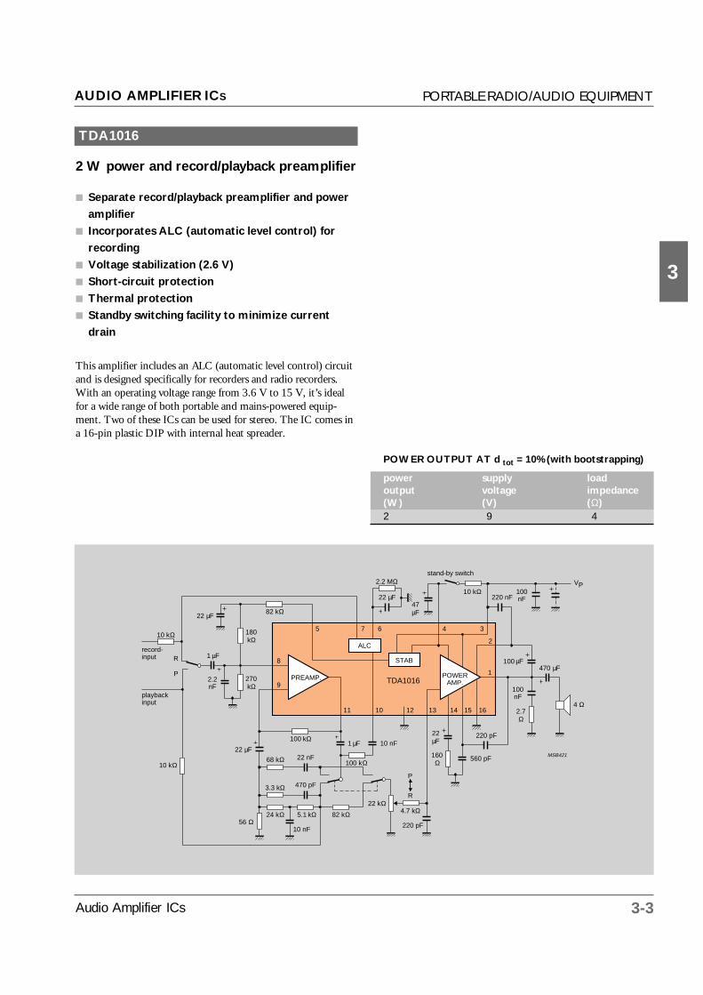
TDA1016
2 W power and record/playback preamplifier
Separate record/playback preamplifier and power
amplifier
Incorporates ALC (automatic level control) for
recording
Voltage stabilization (2.6 V)
Short-circuit protection
Thermal protection
Standby switching facility to minimize current
drain
This amplifier includes an ALC (automatic level control) circuitand is designed specifically for recorders and radio recorders.With an operating voltage range from 3.6 V to 15 V, it’s idealfor a wide range of both portable and mains-powered equip-ment. Two of these ICs can be used for stereo. The IC comes ina 16-pin plastic DIP with internal heat spreader.
MSB421
VP
TDA1016
56 Ω
470 µFPOWER
AMP.PREAMP.
1 µF
24 kΩ 5.1 kΩ
10 nF
3.3 kΩ 470 pF
100 kΩ
82 kΩ
22 kΩ4.7 kΩ
220 pF
10 nF
68 kΩ 22 nF
100 kΩ22 µF
270kΩ
2.2nF
1 µFR
P
10 kΩ
10 kΩ
record-input
playbackinput
180kΩ
STAB
ALC
8
9
5 7 6
11 10 12
22 µF
22µF
160Ω
13 14 15 16
560 pF
220 pF
100nF
2.7Ω
4 Ω
100 µF
2
1
100nF
2.2 MΩ
22 µF10 kΩ
220 nF
stand-by switch
47µF82 kΩ
4 3
P
R
POWER OUTPUT AT d tot = 10% (with bootstrapping)
power supply load output voltage impedance(W) (V) (Ω)2 9 4
AUDIO AMPLIFIER ICS PORTABLE RADIO/AUDIO EQUIPMENT

3-4
3
Audio Amplifier ICs
TDA1308T
60 mW stereo headphone amplifier
Wide temperature range
No switch-on/off clicks
Excellent power supply ripple rejection
Low current drain (typically 3 mA with a 5 V
supply)
Short-circuit resistant
110 dB signal-to-noise ratio
5 V/µs slew rate at unity gain
Large output voltage swing
This is a class-AB stereo driver for delivering up to 60 mW into32 Ω headphones. It is fabricated in a 1 µm CMOS process andis intended primarily for portable digital audio applications. Ithas a supply voltage range from 3 V to 7 V.
It comes an 8-pin SO package for surface mounting.
MLB701
1
7
2
3
5
6
4
8
1 nF
3.9 kΩ
VP
input 1
VREF
input 2
(typ. 2.5 V)TDA1308T
1 nF
3.9 kΩ
10 kΩ
10 kΩ
100 µF
100 µF
100 µF
100 nF
headphones
POWER OUTPUT AT d tot = 10%
power supply load output voltage impedance(mW) (V) (Ω)60 5 32
AUDIO AMPLIFIER ICS PORTABLE RADIO/AUDIO EQUIPMENT

3-5Audio Amplifier ICs
3
TDA7050(T)
150 mW BTL or 2 × 75 mW low-voltage amplifier
Requires no external components in BTL
configuration
Operates with battery supplies from 6 V down to
1.6 V
Very low quiescent current (typically 3.2 mA with
3 V supply)
Closed-loop voltage gain fixed at 26 dB in the
stereo configuration or 32 dB in the BTL configu-
ration (floating differential input, 3 V supply and
32 Ω load)
This low-voltage amplifier is for portable mono (BTL) or stereoapparatus with headphones.
It comes in an 8-pin plastic DIP (TDA7050), or in an 8-pinsmall outline (SO) plastic package for surface mounting(TDA7050T).
MSB405
21
7
TDA7050(T)
47 µF
left channelinput
34
6
47 µF
right channelinput
8
100 nFVP
22 kΩ
22 kΩ
5
MSA612
100nF
PV
7
TDA7050(T)
1
8
2
input
22 kΩ
64
3
POWER OUTPUT AT d tot = 10%
power supply load output voltage impedance(mW) (V) (Ω)mono BTL150 4.5 64140 3 32stereo2 × 75 4.5 322 × 35 3 32
TDA7050(T) in single-ended stereo configuration TDA7050(T) in BTL mono configuration
AUDIO AMPLIFIER ICS PORTABLE RADIO/AUDIO EQUIPMENT

3-6
3
Audio Amplifier ICs
1 W/2 × 1 W BTL amplifiers
No external components required
Excellent overall stability
Output protected against short-circuit
No external heatsink required
Low power consumption
No switch-on or switch-off clicks
Supply voltage range of 3 V to 18 V
Fixed closed-loop voltage gain of 39 dB (6 V supply,
8 Ω load)
The proprietary circuit design of these amplifiers makes use ofthe bridge-tied load (BTL) principle to achieve low-voltageoperation without sacrifice of output power. They are thereforeprimarily intended for battery-powered portable recorders andradios. However, their wide supply voltage range (3 V to 18 V)also makes them suitable for TV.
The TDA7052 comes in an 8-pin plastic DIP and is pin-compatible with half of the TDA7053 which is in a 16-pin plas-tic DIP.
TDA7052/TDA7053
POWER OUTPUT AT d tot = 10%
power supply load output voltage impedance(W) (V) (Ω)TDA70521 6 82 11 25TDA70532 × 1 6 82 × 2 11 25
14 MSA611
100nF
220µF
PV
16
TDA7053
13
2
5
12
9
6
7
1
signalground 2
input 2
signalground 1
input 1
5 kΩ
5 kΩ
10
power ground 1 power ground 2
TDA7053 in BTL stereo configuration
6 MSB420
100nF
220µF
PV
5
TDA7052
8
2
1
3
signalground
input
5 kΩ
power ground
TDA7053 in BTL mono configuration
AUDIO AMPLIFIER ICS PORTABLE RADIO/AUDIO EQUIPMENT
3-7Audio Amplifier ICs
3
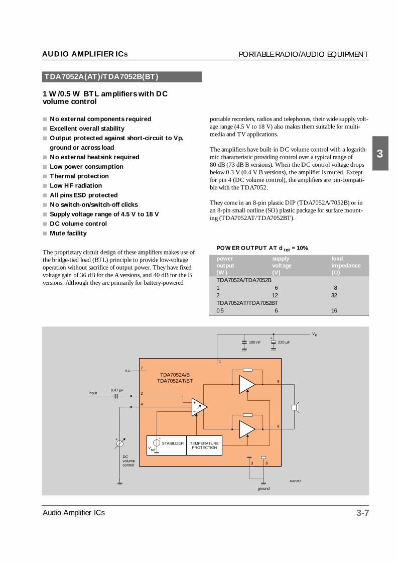
TDA7052A(AT)/TDA7052B(BT)
1 W/0.5 W BTL amplifiers with DC volume control
No external components required
Excellent overall stability
Output protected against short-circuit to Vp,
ground or across load
No external heatsink required
Low power consumption
Thermal protection
Low HF radiation
All pins ESD protected
No switch-on/switch-off clicks
Supply voltage range of 4.5 V to 18 V
DC volume control
Mute facility
The proprietary circuit design of these amplifiers makes use ofthe bridge-tied load (BTL) principle to provide low-voltageoperation without sacrifice of output power. They have fixedvoltage gain of 36 dB for the A versions, and 40 dB for the Bversions. Although they are primarily for battery-powered
POWER OUTPUT AT d tot = 10%
power supply load output voltage impedance(W) (V) (Ω)TDA7052A/TDA7052B1 6 82 12 32TDA7052AT/TDA7052BT0.5 6 16
input0.47 µF
6
MBC281
100 nF 220 µF
1
2
TDA7052A/BTDA7052AT/BT
V P
4
5
8
Vref
STABILIZER TEMPERATUREPROTECTION
3
ground
DCvolumecontrol
7n.c.
AUDIO AMPLIFIER ICS PORTABLE RADIO/AUDIO EQUIPMENT
portable recorders, radios and telephones, their wide supply volt-age range (4.5 V to 18 V) also makes them suitable for multi-media and TV applications.
The amplifiers have built-in DC volume control with a logarith-mic characteristic providing control over a typical range of 80 dB (73 dB B versions). When the DC control voltage dropsbelow 0.3 V (0.4 V B versions), the amplifier is muted. Exceptfor pin 4 (DC volume control), the amplifiers are pin-compati-ble with the TDA7052.
They come in an 8-pin plastic DIP (TDA7052A/7052B) or inan 8-pin small outline (SO) plastic package for surface mount-ing (TDA7052AT/TDA7052BT).

3-8
3
Audio Amplifier ICs
TDA7053A/TDA7053AT
2 × 1 W/2 × 0.5 W BTL amplifiers with DCvolume control
No external components required
Excellent overall stability
Output protected against short-circuit to Vp,
ground or across load
No external heatsink required
Low power consumption.
Thermal protection
Low HF radiation
All pins ESD protected
No switch-on/switch-off clicks
Supply voltage range of 4.5 V to 18 V
DC volume control
Mute facility
These amplifiers are stereo versions of the TDA7052B/TDA7052BT. They use the same proprietary circuit designwhich makes use of the bridge-tied load (BTL) principle to pro-vide low-voltage operation without sacrifice of output power.They have fixed voltage gain of 40 dB. Although they are pri-
POWER OUTPUT AT d tot = 10%
power supply load output voltage impedance(W) (V) (Ω)TDA7053A2 × 1 6 82 × 2 12 32TDA7053AT2 × 0.5 6 16
MSA718 - 2
STABILIZERTEMPERATUREPROTECTIONVref
13
2
4 16
9
8
6 12
14 10
ground
7
input 2
TDA7053ATDA7053AT
5
0.47 µF
input 1
DCvolume
control 1
DCvolume
control 2
0.47 µF
220 µF100 nF
V P
AUDIO AMPLIFIER ICS PORTABLE RADIO/AUDIO EQUIPMENT
marily for battery-powered portable recorders, radios and tele-phones, their wide supply voltage range (4.5 V to 18 V) alsomakes them suitable for multimedia and TV applications.
The amplifiers have built-in DC volume control with a logarith-mic characteristic providing control over a typical range of 73 dB. When the DC control voltage drops below 0.4 V, theamplifier is muted.
They come in a 16-pin plastic DIP (TDA7053A) or in a 16-pinsmall outline (SO) plastic package for surface mounting(TDA7053AT).

3-9Audio Amplifier ICs
3
TDA7056/TDA7057Q
3 W/2 × 3 W BTL amplifiers
No external components required
Excellent overall stability
Output protected against short-circuit
Low power consumption
No switch-on or switch-off clicks
Supply voltage range of 3 V to 18 V
Fixed closed-loop voltage gain of 39 dB
(11 V supply, 16 Ω load)
These BTL amplifiers are primarily for battery-powered port-ables. However, their wide supply voltage range (3 V to 18 V)also makes them suitable for mains-powered applications such asTV.
The TDA7056 comes in a 9-pin plastic SIL medium-powerpackage. The TDA7057Q comes in a 13-pin plastic SIL powerpackage with the pins bent to DIL format.
12 MSB418
100nF
220µF
PV
13
TDA7057Q
11
2
3
10
8
4
5
1
signalground 2
input 2
signalground 1
input 1
5 kΩ
5 kΩ
9
power ground 1 power ground 2
POWER OUTPUT AT d tot = 10%
power supply load output voltage impedance(W) (V) (Ω)TDA70563 11 16
TDA7057Q2 × 3 11 16
TDA7057Q in BTL stereo configuration
7 MSB419
100nF
220µF
PV
6
TDA7056
8
3
2
4
signalground
input
5 kΩ
power ground
TDA7057Q in BTL configuration
AUDIO AMPLIFIER ICS PORTABLE RADIO/AUDIO EQUIPMENT

3-10
3
Audio Amplifier ICs
TDA7056A/TDA7056B
5 W BTL amplifiers with DC volume control
No external components required
Excellent overall stability
Output protected against short-circuit to Vp,
ground or across load
Low power consumption
No switch-on/switch-off clicks
DC volume control
Mute mode
Thermal protection
Low HF radiation
All pins ESD protected
These BTL amplifiers are primarily for battery-powered porta-bles. However, their wide supply voltage range (4.5 V to 18 V)also makes them suitable for mains-powered applications such asmultimedia and TV. They have fixed voltage gain of 36 dB forthe A version, and 40 dB for the B version.
The amplifiers have built-in DC volume control with a logarith-mic characteristic providing control over a typical range of 80 dB (73 dB B version). When the DC control voltage dropsbelow 0.3 V (0.4 V B version), the amplifier is muted.
Both ICs come in a 9-pin plastic SIL package.
POWER OUTPUT AT d tot = 10%
power supply load output voltage impedance(W) (V) (Ω)Both ICs3.5 12 16
TDA7056A5.0 12 8
TDA7056B5.0 12 8
input0.47 µF
7
MBC280
100 nF 220 µF
2
3
TDA7056ATDA7056B
V P
5
6
8
Vref
STABILIZER TEMPERATUREPROTECTION
4
ground
DCvolumecontrol
1n.c.
9n.c.
AUDIO AMPLIFIER ICS PORTABLE RADIO/AUDIO EQUIPMENT

3-11Audio Amplifier ICs
3
TDA7057AQ
2 × 5 W BTL amplifier with DC volume control
No external components required
Excellent overall stability
Output protected against short-circuit to Vp,
ground or across load
Low power consumption
No switch-on/switch-off clicks
DC volume control
Mute mode
Thermal protection
Low HF radiation
All pins ESD protected
This BTL amplifier is a stereo version of the TDA7056B.Although primarily for battery-powered portables, its wide supply voltage range (4.5 V to 18 V) also makes them suitablefor mains-powered applications such as multimedia and TV. Ithas a fixed voltage gain of 40 dB.
MSA715 - 1
STABILIZERTEMPERATUREPROTECTIONVref
11
1
3 13
8
7
5 10
12 9
ground
6
2
input 2
TDA7057AQ4
0.47 µF
input 1
DCvolume
control 1
0.47 µF
DCvolume
control 2
220 µF100 nF
(1)V P
notconnected
POWER OUTPUT AT d tot = 10%
power supply load output voltage impedance(W) (V) (Ω)2 × 3.5 12 162 × 5.0 12 8
AUDIO AMPLIFIER ICS PORTABLE RADIO/AUDIO EQUIPMENT
The amplifier has built-in DC volume control with a logarith-mic characteristic providing control over a typical range of73 dB. When the DC control voltage drops below 0.4 V, theamplifier is muted.
The IC comes in a 13-pin plastic SIL package with the leadsbent to DIL format.

3-12
3
Audio Amplifier ICs
1 W BTL amplifiers
Few external components required
Low saturation voltage of output stage
Gain settable with external resistors
Standby mode controllable by CMOS-compatible
levels
Low standby current
No switch-on/switch-off clicks
High supply-voltage ripple rejection
Thermal protection
Outputs short-circuit safe to ground, VCC and
across load
All pins ESD protected
These amplifiers make use of the bridge-tied load (BTL) princi-ple to achieve low-voltage operation without sacrifice of outputpower. They are therefore primarily for battery-powered applica-tions such as portable recorders and radios and cellular tele-phones. However, their wide supply voltage range (2.2 V to18 V) also makes them suitable for mains powered applicationssuch as multimedia PCs. The amplifiers also feature astandby/mute facility to avoid switch-on/switch-off clicks.
They come in an 8-pin plastic DIP (TDA8541) or in an 8-pinsmall outline (SO) plastic package for surface mounting(TDA8541T).
MGB972
4
STANDBY/MUTE LOGIC
3
6
2
1
7
8
5
R
R
20 kΩ
20 kΩ
IN−
IN+
VCC
SVR
MODE
OUT−
OUT+
GND
−−+
−
−+
TDA8541
TDA8541/TDA8541T
POWER OUTPUT AT d tot = 10%
power supply load output voltage impedance(W) (V) (Ω)1 5 8
AUDIO AMPLIFIER ICS PORTABLE RADIO/AUDIO EQUIPMENT
3-13Audio Amplifier ICs
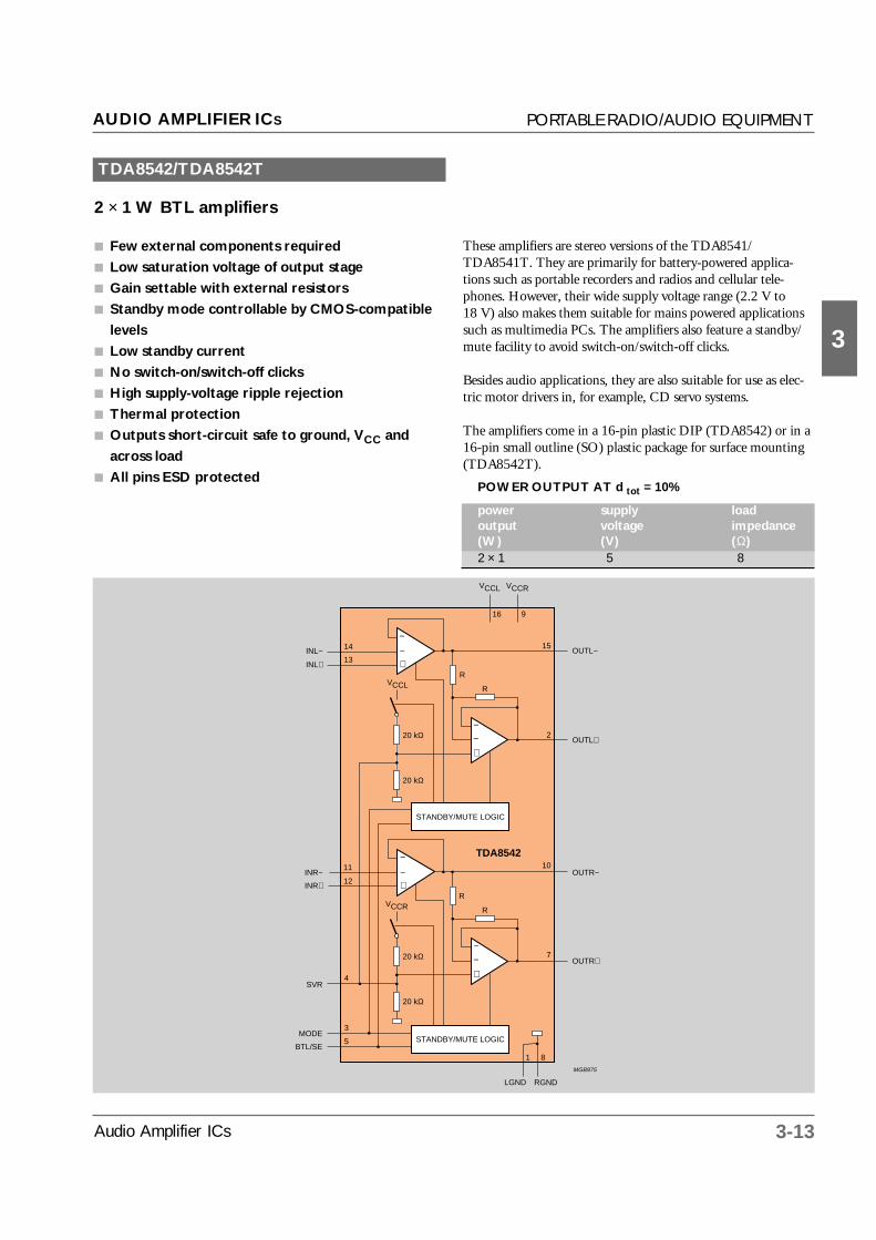
3
2 × 1 W BTL amplifiers
Few external components required
Low saturation voltage of output stage
Gain settable with external resistors
Standby mode controllable by CMOS-compatible
levels
Low standby current
No switch-on/switch-off clicks
High supply-voltage ripple rejection
Thermal protection
Outputs short-circuit safe to ground, VCC and
across load
All pins ESD protected
MGB975
STANDBY/MUTE LOGIC
R
R
20 kΩ
20 kΩ
INL−
INL+
VCCL
OUTL−
OUTL+
−−+
−
−+
STANDBY/MUTE LOGIC
R
R
20 kΩ
20 kΩ
INR−
INR+
VCCR
SVR
MODE
OUTR−
OUTR+
−−+
−
−+
BTL/SE
LGND RGND
VCCL VCCR
16 9
15
2
10
7
1 8
14
13
11
12
4
3
5
TDA8542
TDA8542/TDA8542T
POWER OUTPUT AT d tot = 10%
power supply load output voltage impedance(W) (V) (Ω)2 × 1 5 8
AUDIO AMPLIFIER ICS PORTABLE RADIO/AUDIO EQUIPMENT
These amplifiers are stereo versions of the TDA8541/TDA8541T. They are primarily for battery-powered applica-tions such as portable recorders and radios and cellular tele-phones. However, their wide supply voltage range (2.2 V to18 V) also makes them suitable for mains powered applicationssuch as multimedia PCs. The amplifiers also feature a standby/mute facility to avoid switch-on/switch-off clicks.
Besides audio applications, they are also suitable for use as elec-tric motor drivers in, for example, CD servo systems.
The amplifiers come in a 16-pin plastic DIP (TDA8542) or in a16-pin small outline (SO) plastic package for surface mounting(TDA8542T).

3-14
3
Audio Amplifier ICs
2 W BTL amplifiers
Few external components required
Low saturation voltage of output stage
Gain settable with external resistors
Standby mode controllable by CMOS-compatible
levels
Low standby current
No switch-on/switch-off clicks
High supply-voltage ripple rejection
Thermal protection
Outputs short-circuit safe to ground, VCC and
across load
All pins ESD protected
These BTL amplifiers are primarily for battery-powered applica-tions such as portable recorders and radios and cellular tele-phones. However, their wide supply voltage range (2.2 V to18 V) also makes them suitable for mains powered applicationssuch as multimedia PCs. The amplifiers also feature a standby/mute facility to avoid switch-on/switch-off clicks.
They come in a 16-pin plastic DIP (TDA8543) or in an 16-pinsmall outline (SO) plastic package for surface mounting(TDA8543T).
MSC249
VCC
VCC
20 kΩ
STANDBY/MUTELOGIC
20 kΩ
GND
R
R
6
12
5
4
3
13
OUT+
OUT−IN+
SVR
MODE
IN−
14
11
TDA8543
TDA8543/TDA8543T
POWER OUTPUT AT d tot = 10%
power supply load output voltage impedance(W) (V) (Ω)1 5 82 7.5 81.4 7.5 162 9 161.3 9 25
AUDIO AMPLIFIER ICS PORTABLE RADIO/AUDIO EQUIPMENT

3-15Audio Amplifier ICs
3
2 × 1 W BTL amplifiers with independentchannel standby selection
Independent standby selection of output channels
Few external components required
Low saturation voltage of output stage
Gain settable with external resistors
Standby mode controllable by CMOS-compatible
levels
Low standby current
No switch-on/switch-off clicks
High supply-voltage ripple rejection
Thermal protection
Outputs short-circuit safe to ground, VCC and
across load
All pins ESD protected
MSC261
VCC
VCC1
20 kΩ
STANDBY/MUTELOGIC
20 kΩ
GND1
R
R
11
16
12
4
3
1
GND2
8
OUT2+
OUT2−IN2+
SVR
MODE5
SELECT
IN2−
7
10
STANDBY/MUTELOGIC
RR
14
13
OUT1+
OUT1−IN1+IN1−
2
15
VCC2
9
TDA8547
TDA8547/TDA8547T
POWER OUTPUT AT d tot = 10%
power supply load output voltage impedance(W) (V) (Ω)2 × 1 5 8
AUDIO AMPLIFIER ICS PORTABLE RADIO/AUDIO EQUIPMENT
These BTL stereo amplifiers incorporate standby/mute logic thatallows either one of the output channels to be switched into astandby condition. This feature can be used, for example, forloudspeaker selection. The amplifiers are primarily for battery-powered applications such as portable recorders and radios andcellular telephones. However, their wide supply voltage range(2.2 V to 18 V) also makes them suitable for mains poweredapplications such as multimedia PCs.
The amplifiers come in a 16-pin plastic DIP (TDA8547) or in a16-pin small outline (SO) plastic package for surface mounting(TDA8547T).

3-16
3
Audio Amplifier ICs
1 W BTL amplifiers with digital volume control
One-pin digital volume control (volume setting
with up/down pulses)
Few external components required
Low saturation voltage of output stage
Standby mode controllable by CMOS-compatible
levels
Low standby current
No switch-on/switch-off clicks
High supply-voltage ripple rejection
Thermal protection
Outputs short-circuit safe to ground, VCC and
across load
All pins ESD protected
These BTL mono amplifiers feature digital volume control andstandby/mute logic. They are primarily for battery-poweredapplications such as portable recorders/radios and cellular tele-phones but they are also ideally suited for use in, for example,personal computers.
The amplifiers come in an 8-pin plastic DIP (TDA8551) or inan 8-pin small outline (SO) plastic package for surface mount-ing (TDA8551T).
MSC262
STANDBY/MUTEOPER
GND
R
VCC
R
20 kΩ
7
MODE
2
OUT+5
OUT+8
6
VOLUMECONTROL
TDA8551
SLAVE
MASTER
up/down
in
VCC
1
4
SVT 3
50 kΩ
50 kΩ5 kΩ
TDA8551/TDA8551T
POWER OUTPUT AT d tot = 10%
power supply load output voltage impedance(W) (V) (Ω)1 5 8
AUDIO AMPLIFIER ICS PORTABLE RADIO/AUDIO EQUIPMENT

3-17Audio Amplifier ICs
3
Low-voltage BTL mono amplifiers
Operating voltages down to 1.8 V
Very low quiescent current
Low distortion
No external components required
Differential inputs
Standby mode
No switch-on/switch-off clicks
Outputs short-circuit safe to ground, VCC and
across load
All pins ESD protected
These BTL mono amplifiers operate at voltages from as low as1.8 V up to a maximum of 18 V. They also consume very littlequiescent current. The amplifiers are therefore ideally suited tobattery-powered applications (2 × 1.5 V cells) in, for example,cellular telephones and personal audio equipment. Moreover, adynamic quiescent controller (DQC) feature automaticallyincreases quiescent current at higher frequencies to minimizeHF cross-over distortion. The amplifiers also feature a standby/mute facility to avoid switch-on/switch-off clicks.
They come in an 8-pin plastic DIP (TDA8558) or in an 8-pinsmall outline (SO) plastic package for surface mounting(TDA8558T).
MSC263
VP
OUT−
OUT+
5
7
8
1
TDA8558
OA
GND
DQCOA
OA
STANDBY
4
2
3
8
MUTE
INPUT
INPUTLOGIC
REF VP
VP
POWER OUTPUT AT d tot = 10%
power supply load output voltage impedance(W) (V) (Ω)0.125 3 25
TDA8558/TDA8558T
AUDIO AMPLIFIER ICS PORTABLE RADIO/AUDIO EQUIPMENT

3-18
3
Audio Amplifier ICs
Low-voltage BTL stereo amplifiers
Operating voltages down to 1.9 V
Very low quiescent current
Low distortion
Few external components required
Differential inputs
Can be used as a mono amplifier in BTL or stereo
single-ended (SE) mode
SE mode without need of capacitor in series with
the loudspeaker
Mute and standby mode
No switch-on/switch-off clicks
Outputs short-circuit safe to ground, VCC and
across load
All pins ESD protected
These BTL stereo amplifiers operate at voltages from as low as1.9 V up to a maximum of 30 V and they consume very littlequiescent current. The amplifiers are therefore ideally suited to
+
−+
−
+
−+
−
OA
INPUTLOGIC
V/I
REFERENCE
V/I
1STANDBY
−INV1
INV1
−INV2
INV2
MUTE
MODE
SVRR
n.c. GND
2
3
5
6
4 12BUFFER
OUT2
OUT1
MGD115
11
14
1615
139,10
7
8
VP
VP
VP1VP2
BUFFER
OA
50 kΩ50 kΩ
50kΩ
50kΩ
TDA8559
DQC
DQC
TDA8559/TDA8559T
POWER OUTPUT AT d tot = 10%
power supply load output voltage impedance(W) (V) (Ω)0.035 3 32
BTL mode0.140 3 25
AUDIO AMPLIFIER ICS PORTABLE RADIO/AUDIO EQUIPMENT
battery-powered applications (2 × 1.5 V cells) in, for example,personal audio equipment. They can also be used as a monoamplifier (e.g. in cellular phones) and as a line driver in mains-powered applications without need of any external components.A dynamic quiescent controller (DQC) feature automaticallyincreases quiescent current at higher frequencies to minimizeHF cross-over distortion. The amplifiers also feature a standby/mute facility to avoid switch-on/switch-off clicks.
They come in a 16-pin plastic DIP (TDA8559) or in a 16-pinsmall outline (SO) plastic package for surface mounting(TDA8559T).

4-1Audio Amplifier ICs
4
CAR RADIOS/POWER BOOSTERS
CAR RADIOS/POWER BOOSTERS

4-2 Audio Amplifier ICs
4
MSB412
VP
input
1 µF8
9 7 6 1
2
1000 µF
3
330 kΩ
TDA1010A
5
stand-byswitch
100 nF
1 nF
100nF
4.7 Ω
R L
100 µF
100 nF680 µF
100 nF
4
POWERAMP.
PREAMP.
TDA1010A/TDA1020
Preamplifier plus 3.4 to 12 W power amplifier
Separate preamplifier and power amplifier allows
standby switching
Low-cost of external components
Good ripple rejection
Thermal protection
Output protected against AC short-circuit to
ground
Load dump protection allows the circuit to
tolerate supply voltages as high as 45 V without
damage
High frequency limiting beyond the audible range
in the pre-amplifier and power amplifier suppress-
es supply interference and ignition noise
Standby switching feature with low current
consumption (<1 mA)
Although these mono amplifiers are primarily for use in carradios, their wide supply voltage range (6 V to 24 V) also makesthem attractive for mains-powered radios and tape recordersrequiring output powers up to 12 W.
They come in a 9-pin plastic SIL medium-power packages foreasy mounting.
POWER OUTPUT AT d tot = 10%
power supply load output voltage impedance(W) (V) (Ω)without bootstrap5.5 14.4 4with bootstrap capacitor (TDA1010A/1020)3.4 14.4 86.2 14.4 46.4/12 14.4 2with additional 220 Ω bootstrap resistor between pins 3 and 4 (TDA1010A only)9 14.4 210 18 2
AUDIO AMPLIFIER ICS CAR RADIOS/POWER BOOSTERS

4-3Audio Amplifier ICs
4
MSB411
VP
100 kΩ
1 kΩ
input
0.1 µF2
1
6
4.7 µF
100 µF
5
0.1 µF
12
130.1 µF
22 Ω
11 10
100 kΩ100 kΩ
TDA1510AQTDA1515BQ
3
100 µFstand-by switch
4.7 Ω
100 µF
1mF
1mF 0.1
µF
100 kΩ
4.7 Ω
1 kΩ
4.7 µF
0.1µF
9 8 7
TDA1510AQ/TDA1515BQ
24 W BTL or 2 × 12 W amplifiers
Low offset voltage at output (<50 mV) – important
for BTL
Externally adjustable voltage gain range of 32 dB
to 56 dB in BTL configuration and 26 dB to 50 dB
in stereo configuration (14.4 V supply, 4 Ω load)
High ripple rejection (50 dB at 1 kHz, Rs = 0 Ω)
Load dump and SOAR protection
Protection against AC short-circuit from output to
ground
Thermal protection
Internally limited bandwidth for rejection of HF
interference
Low standby current (<2 mA) to simplify switching
Few external components needed
Additional features of the TDA1515BQ
Low standby current (<100 µA) which allows
switching via TTL circuitry
Outputs protected against AC and DC short-
circuit to ground
Loudspeaker protection in BTL configuration
Outputs protected against short-circuit to ground
in BTL configuration
Protected against reverse polarity supply voltage
POWER OUTPUT AT d tot = 10%
power supply load output voltage impedance(W) (V) (Ω)mono BTL with bootstrap capacitors24 14.4 4stereo with bootstrap capacitors2 × 7 14.4 42 × 12 14.4 2stereo without bootstrap capacitors2 × 6 14.4 4
These class-B output amplifiers can be used in car audio systemsto drive loads down to 1.6 Ω. They have externally adjustablevoltage gain.
They come in 13-pin plastic SIL power packages with the pinsbent to DIL format.
MSB410
VP
4.7 Ω100 kΩ
input
330 pF
680 Ω
0.22 µF2
1
4 6
47 µF
100 µF
(1)
5
0.1 µF100 kΩ
2 kΩ 4.7 µF
100 µF
(1) TDA1515B only
9 8 7
12
130.22 µF
22 Ω
11 10
100 kΩ100 kΩ
TDA1510AQTDA1515BQ
3
47 µFstand-by switch
0.1 µF
TA1510AQ/TDA1515BQ in single-ended stereo configuration TA1510AQ/TDA1515BQ in BTL mono configuration
AUDIO AMPLIFIER ICS CAR RADIOS/POWER BOOSTERS

4-4 Audio Amplifier ICs
4
MSB259
100 nF2.2mF
PV
3
powerground
560 kΩ
TDA1516BQTDA1518BQ
11 10
1
stand-by switch
220 nFinput 1
13220 nF
input 2
7
6
to VP
1 mF2
100µF
input ref.voltage
4
9
8
to VP
1 mF
12VP2
signalground
100 nF2.2mF
PV
3
powerground
5
TDA1516BQ/CQTDA1518BQ
11 10
1
stand-by switch
13
220 nFinput
7
6
to VP
2
input ref.voltage
4
960 kΩ
8
to VP
12VP2
signalground
60 kΩ
60 kΩ
TDA1516BQ/TDA1516CQ/TDA1518BQ
24 W BTL or 2 × 12 W amplifiers
No external components in BTL configuration
Low offset voltage (100 mV) at output (250 mV for
TDA1518BQ) – important for BTL
Fixed closed-loop voltage gain (14.4 V supply, 4 Ωload) of 26 dB for BTL (TDA1516BQ and
TDA1516CQ) and 20 dB for stereo (TDA1516BQ).
The figures for the TDA1518BQ are 46 dB (BTL)
and 40 dB (stereo)
High supply voltage ripple rejection (48 dB
between 100 Hz and 10 kHz, Rs = 0 Ω)
Load dump protection
Output protected against AC and DC short-circuit
to ground or supply rail
Thermal protection
Reverse polarity safe
Standby feature with switch-on voltage of 0 V to
2 V at pin 11 and a switch-on current of only 12 µA
to allow use of an inexpensive switch. The standby
supply current is <100 µA. The voltage at pin 11
for normal operation is >8.5 V
Mute facility with switch-on voltage of 3 V to 6.4 V
at pin 11 to eliminate switch-on/switch-off clicks.
The supply current in the muted condition is
40 mA
Identical inputs (inverting and non-inverting)
Few external components needed in stereo
configuration
Like the TDA1510AQ/1515BQ these are car audio class-Bpower amplifiers but with internally fixed gain for excellentchannel balance (within 1 dB). The three types are virtuallyidentical except for their gain. The TDA1516CQ is identical tothe TDA1516BQ except that it consumes very little current inshort-circuit to ground condition (typically 5.5 mA) and is onlysuitable for operation in BTL mode.
The ICs come in 13-pin plastic SIL power packages with thepins bent to DIL format.
TDA1516BQ/TDA1516CQ/TDA1518BQ in BTL mono configuration TDA1516BQ/TDA1518BQ in single-ended stereo configuration
POWER OUTPUT AT d tot = 10%
power supply load output voltage impedance(W) (V) (Ω)mono BTL with bootstrapping24 14.4 4mono BTL without bootstrapping22 14.4 4stereo with bootstrapping2 × 7 14.4 42 × 12 14.4 2stereo without bootstrapping2 × 6 14.4 42 × 11 14.4 2
AUDIO AMPLIFIER ICS CAR RADIOS/POWER BOOSTERS
4-5Audio Amplifier ICs
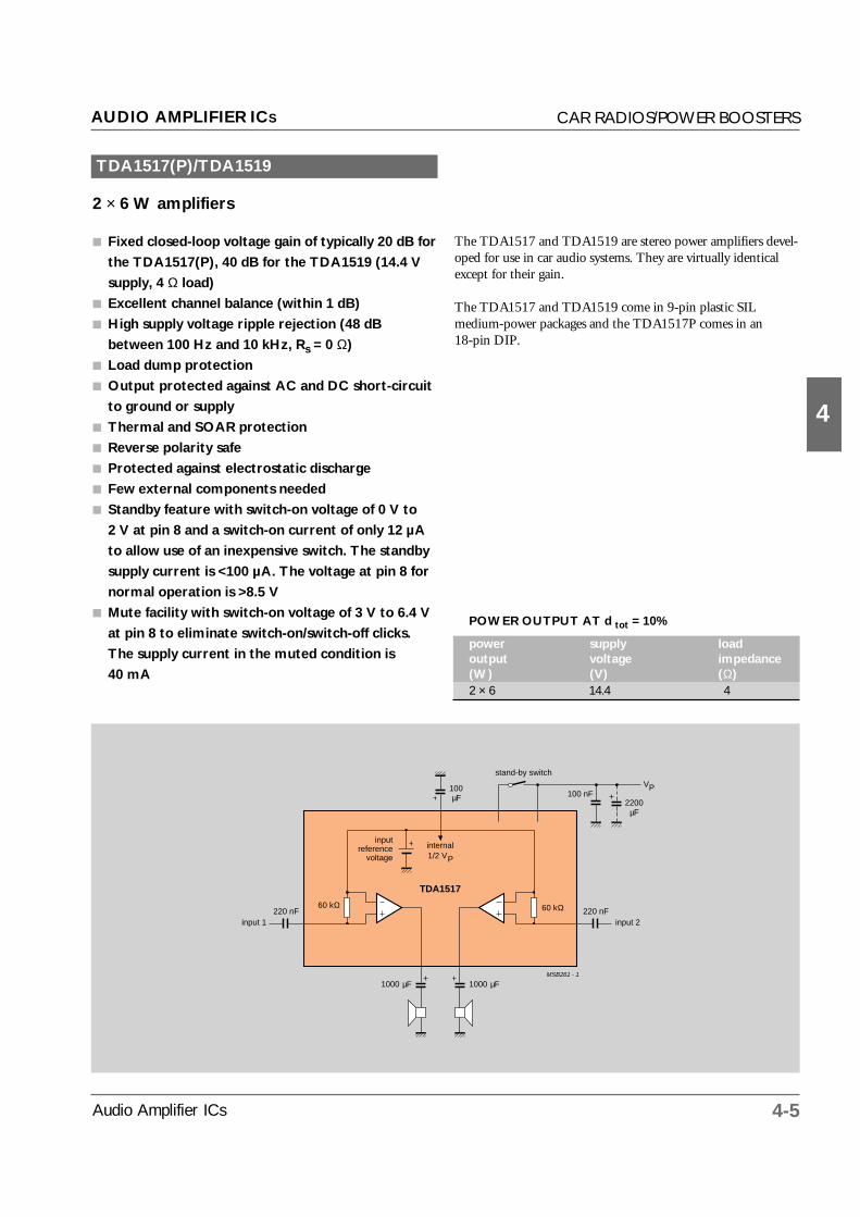
4
MSB261 - 1
100 nFPV
60 kΩ
TDA1517
stand-by switch
220 nFinput 1
1000 µF
inputreference
voltage
220 nFinput 2
1000 µF
2200µF
internal1/2 VP
100µF
60 kΩ
TDA1517(P)/TDA1519
2 × 6 W amplifiers
Fixed closed-loop voltage gain of typically 20 dB for
the TDA1517(P), 40 dB for the TDA1519 (14.4 V
supply, 4 Ω load)
Excellent channel balance (within 1 dB)
High supply voltage ripple rejection (48 dB
between 100 Hz and 10 kHz, Rs = 0 Ω)
Load dump protection
Output protected against AC and DC short-circuit
to ground or supply
Thermal and SOAR protection
Reverse polarity safe
Protected against electrostatic discharge
Few external components needed
Standby feature with switch-on voltage of 0 V to
2 V at pin 8 and a switch-on current of only 12 µA
to allow use of an inexpensive switch. The standby
supply current is <100 µA. The voltage at pin 8 for
normal operation is >8.5 V
Mute facility with switch-on voltage of 3 V to 6.4 V
at pin 8 to eliminate switch-on/switch-off clicks.
The supply current in the muted condition is
40 mA
POWER OUTPUT AT d tot = 10%
power supply load output voltage impedance(W) (V) (Ω)2 × 6 14.4 4
AUDIO AMPLIFIER ICS CAR RADIOS/POWER BOOSTERS
The TDA1517 and TDA1519 are stereo power amplifiers devel-oped for use in car audio systems. They are virtually identicalexcept for their gain.
The TDA1517 and TDA1519 come in 9-pin plastic SIL medium-power packages and the TDA1517P comes in an 18-pin DIP.

4-6 Audio Amplifier ICs
4
TDA1519A/TDA1519B
22 W BTL or 2 × 11 W/12 W BTL or 2 × 6 W amplifiers
No external components in BTL configuration
Very few external components in stereo
configuration
Low offset voltage at output (250 mV) – important
for BTL
Fixed closed-loop voltage gain (14.4 V supply, 4 Ωload) of 46 dB for BTL and 40 dB for stereo
High supply voltage ripple rejection (48 dB
between 100 Hz and 10 kHz, Rs = 0 Ω)
Load dump protection
Output protected against AC and DC short-circuit
to ground or supply rail
Thermal protection
Reverse polarity safe
Standby feature with switch-on voltage of 0 V to
2 V at pin 8 and a switch-on current of only 12 µA
to allow use of an inexpensive switch. The standby
supply current is <100 µA. The voltage at pin 8 for
normal operation is >8.5 V
POWER OUTPUT AT d tot = 10%
power supply load output voltage impedance(W) (V) (Ω)mono BTL (TDA1519A/1519B)22/12 14.4 4stereo (TDA1519A/1519B)2 × 11/6 14.4 4
Mute facility with switch-on voltage of 3.3 V to
6.4 V at pin 8 to eliminate switch-on/switch-off
clicks. The supply current in the muted condition
is 40 mA
Identical inputs (inverting and non-inverting)
These are car audio class-B power amplifiers with internallyfixed gain for excellent channel balance (within 1 dB). The twotypes are virtually identical except for their output power.
The TDA1519A comes in a 9-pin power plastic SIL packagewith or without the pins bent to DIL format. The TDA1519Bcomes in a 9-pin plastic medium-power SIL package.
MSB260
100 nF2.2mF
PV
2
4
TDA1519A(B)
8 7
1
stand-by switch
220 nFinput 1
9220 nF
input 2
5
60 kΩ
6
1 mFinternal
Vref.
60 kΩ
3
1/2 VP
100 nF2.2mF
PV
2
4
TDA1519A(B)
8 7
1
stand-by switch
220 nFinput
9
5
60 kΩ
6
internalVref.
3
1/2 VP
60 kΩ
TDA1519A(B) in BTL mono configuration TDA1519A(B) in single-ended stereo configuration
AUDIO AMPLIFIER ICS CAR RADIOS/POWER BOOSTERS

4-7Audio Amplifier ICs
4
TDA1552Q/TDA1553Q/CQ/TDA1557Q
2 × 22 W BTL amplifiers
Very few external components
Low offset voltage at output (150 mV; 250 mV for
the TDA1557Q) – important for BTL
Fixed closed-loop voltage gain (14.4 V supply, 4 Ωload) of 26 dB (46 dB for the TDA1557Q)
High supply voltage ripple rejection (48 dB
between 100 Hz and 10 kHz, Rs = 0 Ω)
Load dump protection
Output protected against AC and DC short-circuit
to ground or supply rail
Low current consumption in short-circuit to
ground condition (typ. 5.5 mA)
Thermal protection
Reverse polarity safe
Standby feature with switch-on voltage of 0 V to
2 V at pin 11 and a switch-on current of only 25 µA
to allow use of an inexpensive switch. The standby
supply current is <100 µA. The voltage at pin 11
for normal operation is >8.5 V
Mute facility with switch-on voltage of 3.3 V to
6.4 V at pin 11 to eliminate switch-on/switch-off
clicks
TDA1553CQ incorporates mute/standby/normal
operation selection with CMOS-compatible switch-
ing levels
Loudspeaker protection limits voltage across the
associated loudspeaker to 1 V or less in the event
any of the outputs being short-circuited to ground
(TDA1553Q, TDA1553CQ and TDA1557Q)
These are car audio class-B power amplifiers with internallyfixed gain for excellent channel balance (within 1 dB). The fourtypes are virtually identical except that the TDA1553Q,TDA1553CQ and TDA1557Q incorporate loudspeaker protec-tion and that the TDA1557Q has a 20 dB higher gain.
They come in 13-pin plastic SIL power packages with the pinsbent to DIL format.
POWER OUTPUT AT d tot = 10%
power supply load output voltage impedance(W) (V) (Ω)2 × 22 14.4 4
100 nF2.2mF
PV
5
signal ground
power ground (substrate)
4
6
60 kΩ
12
not connected
TDA1552Q/TDA1557Q
11 3 10
1
mute/stand-by
2V ref
220 nFinput 1
9
7
13220 nF
input 2
8
60 kΩ
MSB257
100 nF2.2mF
PV
5
signal ground
power ground (substrate)
4
6
12
TDA1553Q(CQ)
11 3 10
1
mute/stand-by
2V ref
220 nFinput 1
9
7
13220 nF
input 2
8
60 kΩ
60 kΩ
TDA1552Q/TDA1557Q in BTL stereo configuration TDA1553Q/TDA1553CQ in BTL stereo configuration
AUDIO AMPLIFIER ICS CAR RADIOS/POWER BOOSTERS
* connected to Vref on the TDA1557Q

4-8 Audio Amplifier ICs
4
TDA1554Q/TDA1555Q/TDA1558Q
2 × 22 W BTL or 4 × 11 W amplifiers
Very few external components
Low offset voltage at output (100 mV, 250 mV for
the TDA1558Q) – important for BTL
Fixed closed-loop voltage gain (14.4 V supply, 4 Ωload) of 20 dB (26 dB in BTL), 40 dB (46 dB in
BTL) for the TDA1558Q
High supply voltage ripple rejection (48 dB
between 100 Hz and 10 kHz, Rs = 0 Ω)
Load dump protection
Output protected against AC and DC short-circuit
to ground or supply rail
Thermal protection
Reverse polarity safe
Standby feature with switch-on voltage of 0 V to
2 V at pin 14 and a switch-on current of only 12 µA
to allow use of an inexpensive-pensive switch. The
standby supply current is >100 µA. The voltage at
pin 14 for normal operation is >8.5 V
Mute facility with switch-on voltage of 3.3 V to
6.4 V at pin 14 to eliminate switch-on/switch-off
clicks
Identical inputs (inverting and non-inverting)
Distortion detector senses output clipping and for
clip distortion of 3.5% it supplies a current of
50 µA typical for reducing the drive via a sound
processor or DC volume control (TDA1555Q only)
These are class-B power amplifiers with internally fixed gain forexcellent channel balance (within 1 dB). They are for BTLstereo or quad (front and rear stereo) car audio applications. Thethree types are virtually identical except that the TDA1555Qincorporates distortion detection, and the TDA1558Q has 20 dB higher gain.
They come in 17-pin plastic SIL power packages with the pinsbent to DIL format.
POWER OUTPUT AT d tot = 10%
power supply load output voltage impedance(W) (V) (Ω)BTL stereo2 × 22 14.4 4quad4 × 11 14.4 24 × 6 14.4 4
9
MSB255
100 nF2.2mF
PV
7
signal ground
power ground (substrate)
1 mF
1 mF
6
860 kΩ
15
distortion detector
TDA1554Q/1555Q/1558Q
14 5 13
1
2
mute/stand-by switch
4V /2P V ref
220 nF
220 nF
input 1
input 2
100 µF
supplyripplerejection
1 mF
1 mF
12
10
60 kΩ
17
16
220 nF
220 nF
input 3
input 4
1139
100 nF2.2mF
PV
7
signal ground
power ground (substrate)
6
860 kΩ
15
distortion detector
TDA1554Q/1555Q/1558Q
14 5 13
1
2
mute/stand-by switch
4V /2P V ref
220 nFinput 1
supplyripplerejection
12
10
60 kΩ
17
16
220 nFinput 2
113
not connected not connected
60 kΩ
60 kΩ
60 kΩ
60 kΩ
TDA1554Q/TDA1555Q/TDA1558Q in BTL stereo configuration TDA1554Q/TDA1555Q/TDA1558Q in single-ended quad (dual stereo)configuration
AUDIO AMPLIFIER ICS CAR RADIOS/POWER BOOSTERS
* not connected on the TDA1554Q connected to Vrefon the TDA1558Q

4-9Audio Amplifier ICs
4
TDA1556Q
2 × 22 W BTL amplifier with differentialinputs
Very few external components
Differential inputs
High CMRR (>64 dB)
High supply voltage ripple rejection (48 dB
between 100 Hz and 10 kHz, Rs = 0 Ω)
Low offset voltage at output (150 mV) – important
for BTL
Fixed closed-loop voltage gain (14.4 V supply, 4 Ωload) of 26 dB
Load dump protection
Thermal protection
Outputs protected against AC and DC short-
circuit to ground, supply rail or across load
Low current consumption in short-circuit to
ground condition (5.5 mA)
Reverse polarity safe
Loudspeaker protection limits voltage across the
associated loudspeaker to 1 V or less in the event
any of the outputs being short-circuited to ground
Standby feature with switch-on voltage of 0 V to
2 V at pin 14 and a switch-on current of only 25 µA
to allow use of an inexpensive switch. The standby
supply current is <100 µA. The voltage at pin 14
for normal operation is >8.5 V
Mute facility with switch-on voltage of 3.3 V to
6.4 V at pin 14 to eliminate switch-on/switch-off
clicks
Distortion detector senses output clipping. It pro-
vides 50 µA typical for a clip distortion of 3.5% to
reduce input drive via a sound processor or DC
volume control
This is a class-B power amplifier with internally fixed gain forexcellent channel balance (within 1 dB). The amplifier has twodifferential input stages with high Common Mode RippleRejection (CMRR) which makes it very attractive for car radiobooster applications. The TDA1556Q also incorporates aDynamic Distortion Detector (DDD) and loudspeaker protec-tion.
It comes in a 17-pin plastic SIL power package with the pinsbent to DIL format.
POWER OUTPUT AT d tot = 10%
power supply load output voltage impedance(W) (V) (Ω)2 × 22 14.4 4
15Vref
9
3
n.c.
n.c.
7 11
MBC271
TDA1556Q
100nF
DDD on/mute/stand-by
4 14 5 13
VP
2200µF
4.7 µF
220 nF
220 nF
16
17
10
12
220 nF
220 nF
1
2
6
8
input 1
input 2
input 3
input 4
60 kΩ
60 kΩ
60 kΩ
60 kΩ
AUDIO AMPLIFIER ICS CAR RADIOS/POWER BOOSTERS
TDA1556Q in BTL stereo configuration

4-10 Audio Amplifier ICs
4
TDA1560Q
40 W BTL class-H amplifier
Few external components
Very high output power
Low power dissipation when reproducing music
Fixed closed-loop voltage gain (14.4 V supply, 8 Ωload) of 30 dB
High supply voltage ripple rejection of 55 dB over
the frequency range 100 Hz to 10 kHz, Rs = 0 Ω)
Switches to low output power if the heatsink over-
heats
Low crossover distortion
No switch-on/off clicks
Thermal protection
Mode switch for standby (0 to 1.2 V)/mute (2.6 to
3.5 V)/class-B (4.5 to 7 V)/class-H (8.5 V to Vp)
operation. Maximum switch current is only 20 µA
to allow use of an inexpensive-pensive switch
Low offset voltage at the output – important for
BTL
Load dump protection
Load short-circuit safe to ground or Vp
Pins protected against ESD
Thermal protection
Primarily for car audio applications, this IC uses class-H amplifi-er techniques so that, with a 14.4 V supply and minimalheatsinking, it can deliver 40 W into an 8 Ω load. For the firsttime, this allows a 4 × 40 W car radio to be assembled in a stan-dard DIN-sized car radio case.
Below 10 W the IC acts as a normal BTL amplifier. At higheroutputs, the internal supply voltage is doubled by adding thecharge stored on external capacitors. This allows the power out-put to increase to 40 W.
The amplifier comes in a 17-pin plastic SIL power package withthe pins bent to DIL format.
SUPPLY
SUPPLYTEMPERATURE
SENSOR
INPUT ANDFEEDBACK
CIRCUIT
13 10
2200 F 100 nF 2200 F
ground
9
MCD333 - 3
output 2 (+)
voltagereference
V
POWERSTAGE
POWERSTAGE
5 8
2200 F
7
11
1
0.22 F
1
0.22 F
0.22 F
15
mode select switch16
150 k
1Ck
Ck
S1
2
4
R = 100 kex
150 nF
150 nF
input (+)input
input (–)
output 1 (–)
15 k
10 F
10 k17
disable
disable
VP
VP
12 6
Vref
TDA1560Q
Ω
Ω
µ
2
0.22 Fµ
Ω
µ
µ
µ
Ω
Ω
150 k Ω
µ
Ω
Ω
µ
µ
3
µ
2
0.22 F
Ω
P
LOAD DUMPTEMPERATUREAND CURRENTPROTECTION
14diagnosticoutput
POWER OUTPUT AT d tot = 10%
power supply load output voltage impedance(W) (V) (Ω)17 14.4 440 14.4 8
AUDIO AMPLIFIER ICS CAR RADIOS/POWER BOOSTERS

4-11Audio Amplifier ICs
4
TDA1561Q
2 × 23 W high efficiency power amplifier
Low power dissipation since the amplifier switches
from SE mode into BTL mode only when receiving
high-amplitude signals
High common-mode rejection ratio
Mute/standby/BTL-disable switch (mode select pin)
Zero-crossing mute
Load dump protection
Short-circuit safe to ground, Vp and across load
Loudspeaker protection
Automatically switches to SE mode at excessive
crystal temperature
Thermal protection
This power amplifier normally operates in low-power single-ended mode and switches to high-power BTL mode only whenlarge amplitude signals are received from the preamplifer. TheTDA1561Q therefore dissipates only about 55% of the powerdissipated by a conventional power amplifier (measured at aver-age maximum music power) which means heatsinks can besmaller. Primarily for car audio applications, the amplifier is alsoideal for multimedia systems and active loudspeakers.
The TDA1561Q comes in a 13-pin plastic SIL power packagewith the pins bent to DIL format.
MLD214
REFERENCESOURCES
MUTE/STANDBY
THERMAL/SHORT-CIRCUIT
PROTECTION
HIGHERTEMPERATURE
BTL DISABLE
0.5VP
MUTE
R
MUTE
R
7
VP
12
3
13
2
1IN1
IN2
CIN
MODE
1/2R
HV
4
GND1
10
GND2
6
5
11
9
8OUT2
OUT2
OUT1
OUT1
C
TDA1561Q
P
11
POWER OUTPUT AT d tot = 10%
power supply load output voltage impedance(W) (V) (Ω)2 × 23 14.4 4
AUDIO AMPLIFIER ICS CAR RADIOS/POWER BOOSTERS

4-12 Audio Amplifier ICs
4
TDA8560Q/TDA8563Q/TDA8563AQ
2 × 40 W BTL amplifiers
Very few external components
High supply voltage ripple rejection (>50 dB
between 100 Hz and 10 kHz, Rs = 0 Ω)
Low offset voltage (150 mV) at output (200 mV for
TDA8560Q) – important for BTL
Fixed closed-loop voltage gain (14.4 V supply, 4 Ωload) of 26 dB (TDA8563Q/TDA8563AQ) or 40 dB
(TDA8560Q)
Load dump protection
Thermal protection
Outputs protected against AC and DC short-
circuit to ground, supply rail or across load
Low current consumption in short-circuit to
ground condition
Reverse polarity safe
Standby feature with switch-on voltage of 0 V to
2 V at pin 11 and a switch-on current of only 15 µA
to allow use of an inexpensive switch. The standby
supply current is <100 µA. The voltage at pin 11
for normal operation is >8.5 V
Mute facility with switch-on voltage of 3.3 V to
6.4 V at pin 11 to eliminate switch-on/switch-off
clicks
Diagnostic facility senses distortion, load short-
circuit and temperature
Pins protected against ESD
Low thermal resistance
These are class-B power amplifiers with internally-fixed voltagegain for excellent channel balance (within 1 dB). They are pri-marily for car audio applications. The amplifiers are distinguish-able by their closed-loop voltage gain. The gain of theTDA8560Q is 40 dB, and that of the TDA8563Q andTDA8563AQ is 26 dB.
A diagnostic facility senses distortion, load short-circuit andtemperature. At onset of distortion (10% THD in theTDA8560Q/TDA8663Q, 2.5% THD in the TDA8563AQ) ortemperature >150 °C, the diagnostic output signal can be usedto reduce the input drive via a sound processor or DC volumecontrol. For load short-circuit or output short-circuit to groundor supply, the outputs are switched-off until the short-circuit isremoved.
The ampliers come in 13-pin plastic SIL power packages withthe pins bent to DIL format.
POWER OUTPUT AT d tot = 10%
power supply load output voltage impedance(W) (V) (Ω)2 × 21 13.2 42 × 25 14.4 42 × 35 13.2 22 × 40 14.4 2
MLB666 - 2
100nF
mode switch
11 3 10
470 nF1
4
6
470 nF13
9
7
5 8
VP
TDA8560QTDA8563Q
2200µF
30kΩ
referencevoltage
2ground (signal)
30kΩ
input 2
input 1
power ground (substrate)
12
10 kΩ
VP
diagnosticoutput
AUDIO AMPLIFIER ICS CAR RADIOS/POWER BOOSTERS

4-13Audio Amplifier ICs
4
TDA8561Q/TDA8564Q
2 × 24 W BTL or 4 × 12 W amplifiers
Very few external components Low offset voltage (150 mV) at output (250 mV for
TDA8564Q) – important for BTL High supply voltage ripple rejection (>48 dB
between 100 Hz and 10 kHz, Rs = 0 Ω) Load dump protection Output protected against AC and DC short-circuit
to ground or supply rail Low current consumption (40 mA) during any
short-circuit condition Thermal protection Reverse polarity safe Standby feature with switch-on voltage of 0 V to
2 V at pin 14 and a switch-on current of only 12 µAto allow use of an inexpensive-pensive switch. Thestandby supply current is >100 µA. The voltage atpin 14 for normal operation is >8.5 V
Mute facility with switch-on voltage of 3.3 V to 6.4 Vat pin 14 to eliminate switch-on/switch-off clicks
Identical inputs (inverting and non-inverting) Diagnostic facility senses distortion, load short-
circuit and temperature Pins protected against ESD Low thermal resistance
These are class-B power amplifiers with internally-fixed gain forexcellent channel balance (within 1 dB). They are for BTLstereo or quad (front and rear stereo) car audio applications. Thetwo types are identical except that the TDA8561Q has a fixedclosed-loop voltage gain of 26 dB (BTL)/20 dB (single-ended)whereas that of the TDA8564Q 46 dB (BTL) and 40 dB (single-ended).
A diagnostic facility senses distortion, load short-circuit andtemperature. At onset of distortion or temperature >150 °C, thediagnostic output signal can be used to reduce the input drivevia a sound processor or DC volume control. For load short-circuit or output short-circuit to ground or supply, the outputsare switched-off until the short-circuit is removed.
The amplifiers come in 17-pin plastic SIL power packages withthe pins bent to DIL format.
POWER OUTPUT AT d tot = 10%
power supply load output voltage impedance(W) (V) (Ω)BTL stereo2 × 24 14.4 4quad4 × 7 14.4 44 × 12 14.4 2
MEA862 - 2
100nF
16 5 13
220 nF1
6
8
7 11
VP
TDA8561QTDA8564Q
2200µF
60kΩ
2ground (signal)
10kΩ
14
9not connected
3inverting input 2
60kΩ
60kΩ
referencevoltage
220 nF17
12
60kΩ
non-invertinginput 4
4
1510
power ground (substrate)
non- invertinginput 1
supply voltageripple rejection
inverting input 3
diagnostic
modeswitch
MEA863 - 2
100nF
16 5 13
220 nF1
6
8
7 11
VP
TDA8561QTDA8564Q
2200µF
60kΩ
2ground (signal)
10kΩ
14
9not connected
3invertinginput 2
60kΩ
60kΩ
referencevoltage
220 nF
1712
60kΩ
non-invertinginput 4
4
1510
power ground (substrate)
non- invertinginput 1
supply voltageripple rejection
invertinginput 3
220 nF
1/2Vp
1000 µF
220 nF
1000 µF
1000 µF
1000 µF
modeswitch
TDA8561Q/TDA8564Q in BTL stereo configuration left, and in single-ended quad (front and rear stereo) configuration
AUDIO AMPLIFIER ICS CAR RADIOS/POWER BOOSTERS

4-14 Audio Amplifier ICs
4
TDA8562Q/TDA8565Q
4 × 12 W single-ended amplifier
Very few external components
High supply voltage ripple rejection (>48 dB
between 100 Hz and 10 kHz, Rs = 0 Ω)
Load dump protection
Output protected against AC and DC short-circuit
to ground or supply rail
Low current consumption (40 mA) during any
short-circuit condition
Identical inputs
Thermal protection
Reverse polarity safe
Standby feature with switch-on voltage of 0 V to
2 V at pin 8 and a switch-on current of only 12 µA
to allow use of an inexpensive switch. The standby
supply current is <100 µA. The voltage at pin 8 for
normal operation is >8.5 V
Mute facility to eliminate switch-on/switch-off
clicks
Diagnostic facility for sensing distortion, short-
circuit and temperature
Pins protected against ESD
Low thermal resistance
These are car audio class-B power amplifiers with internallyfixed gain for excellent channel balance (within 1 dB). They arefor quad (front and rear stereo) car audio applications. The twotypes are identical except that the TDA8562Q has a fixedclosed-loop voltage gain of 20 dB, whilst that of theTDA8565Q is 20 dB higher.
A diagnostic facility senses distortion, load short-circuit andtemperature. At onset of distortion or temperature >150 °C, thediagnostic output signal can be used to reduce the input drivevia a sound processor or DC volume control. For load short-circuit or output short-circuit to ground or supply, the outputsare switched-off until the short-circuit is removed
The amplifiers come in 17-pin plastic SIL power packages withthe pins bent to DIL format.
MEA867 - 2
100nF
16 5 13
220 nF1
6
8
7 11
VP
TDA8562QTDA8565Q
2200µF
60kΩ
2ground (signal)
10kΩ
9not connected
3input 2
60kΩ
60kΩ
referencevoltage
220 nF
1712
60kΩ
input 4
4
1510
power ground (substrate)
input 1
supplyvoltageripplerejection
input 3220 nF
V /2p
1000 µF
220 nF
100 µF
14
diagnostic
1000 µF
1000 µF
1000 µF
modeswitch
POWER OUTPUT AT d tot = 10%
power supply load output voltage impedance(W) (V) (Ω)4 × 7 14.4 44 × 12 14.4 2
AUDIO AMPLIFIER ICS CAR RADIOS/POWER BOOSTERS

4-15Audio Amplifier ICs
4
TDA8566Q
2 × 25 W BTL power amplifier with differential inputs
Differential inputs
Very high Common Mode Rejection Ratio
High common mode input signal handling capacity
Very few external components
High output power
Low offset voltage at output (<100 mV) –
important for BTL
Fixed gain
Diagnostic facility for sensing distortion, short-
circuit and temperature
Good ripple rejection
Mode-select switch (operating, mute and standby)
Load dump protection
Short-circuit proof to ground, to Vp and across the
load
Low power dissipation in any short circuit
condition
Thermally protected
Reverse-polarity safe
Pins protected against ESD
No switch-on/switch-off clicks
Low thermal resistance
This is a class-B BTL stereo power amplifier. It features a high-impedance fully-differential balanced input stage that’s alsocapable of operating in single-ended mode (with one inputcapacitively coupled to an audio ground).
A diagnostic facility senses distortion, load short-circuit andtemperature. At onset of distortion or temperature >145 °C, thediagnostic output signal can be used to reduce the input drivevia a sound processor or DC volume control. For load short-cir-cuit or output short-circuit to ground or supply, the outputs areswitched-off until the short-circuit is removed.
The amplifier comes in 17-pin plastic SIL power package withthe pins bent to DIL format.
POWER OUTPUT AT d tot = 10%
power supply load output voltage impedance(W) (V) (Ω)2 × 25 14.4 42 × 40 14.4 2
+
−
+
−
CM
VA
(9×)
2.3 kΩ
2.3kΩ
muteswitch
+
−
+
−
CM
VA
VA
1×
standbyreference
voltage
standbyswitch
mutereferencevoltage
Vref muteswitch
CLIP
(9×)
2.3 kΩ
2.3kΩ
60kΩ
60kΩ
60kΩ
60kΩ
muteswitch
+
−
+
−
CM
VA
(9×)
2.3 kΩ
2.3kΩ
muteswitch
+
−
+
−
CM
VA
11 7
12
10
15
4
TDA8566Q
14
8
6
1351
2
3
16
17
VP2VP1
PGND2 PGND1
OUT2−
OUT2+
OUT1−
OUT1+IN1−
IN1+
IN2−
IN2+
SGND
n.c.
DIAG
MODE
CLIP
MGD105
(9×)
2.3 kΩ
2.3kΩ
muteswitch
9
DIAG
AUDIO AMPLIFIER ICS CAR RADIOS/POWER BOOSTERS

4-16 Audio Amplifier ICs
4
TDA8567Q/TDA8568Q/TDA8569Q
4 × 25 W BTL amplifiers
Very few external components
High output power
Low offset voltage at output (TDA8567Q &
TDA8569Q < 150 mV, TDA8568Q < 200 mV) –
important for BTL
Diagnostic facility for sensing distortion, short-
circuit and temperature
Good ripple rejection
Mode-select switch (operating, mute and standby)
Load dump protection
Short-circuit proof to ground, to Vp and across the
load
Low power dissipation in any short circuit
condition
Thermally protected
Reverse-polarity safe
Pins protected against ESD
No switch-on/switch-off clicks
Low thermal resistance
These are class-B power amplifiers with internally fixed gain forexcellent channel balance. They are for quad (front and rearstereo) car audio applications. The TDA8567Q andTDA8569Q have a fixed closed-loop voltage gain of 26 dB,whilst that of the TDA8568Q is 40 dB. The TDA8569, more-over, can drive loads down to 2 Ω.
A diagnostic facility senses distortion, load short-circuit andtemperature. At onset of distortion or temperature >145 °C, thediagnostic output signal can be used to reduce the input drivevia a sound processor or DC volume control. For load short-circuit or output short-circuit to ground or supply, the outputsare switched-off until the short-circuit is removed
The amplifiers come in 23-pin plastic SIL power packages withthe pins bent to DIL format.
POWER OUTPUT AT d tot = 10%
power supply load output voltage impedance(W) (V) (Ω)TDA8567Q/TDA8568Q/TDA8569Q4 × 25 14.4 4
VDIAGDIAGNOSTIC9
MSC264
OUT1+
OUT1−
+
−
+
−
Vref
2IN1
IN2
4
23168115
10
MODE VP1 VP2 VP3 VP4
211863
PGND1 PGND2 PGND3 PGND4
30 kΩ
OUT2+
OUT2−
+
−
+
−
7
5
11
30 kΩ
OUT3+
OUT3−
+
−
+
−
Vref
17IN3
SGND TDA8567Q/TDA8568Q/TDA8569Q
IN4
19
13
12
30 kΩ
OUT4+
OUT4−
+
−
+
−
22
20
14
30 kΩ
AUDIO AMPLIFIER ICS CAR RADIOS/POWER BOOSTERS

4-17Audio Amplifier ICs
4
TDA8574(T)
Dual common-mode rejection differentialline drivers
Class-H operation means that output voltage
swings are greater than the supply voltage
High supply voltage ripple rejection
Low distortion (0.003% THD at 1 kHz with
Vo(rms) = 3 V)
Low noise (noise output of typ. 5 µV)
Supply voltage range of 6 V to 12 V
All pins ESD protected
These two-channel class-H amplifiers with single-ended outputsoffer 8 dB voltage gain and low distortion. They’re principallyfor eliminating ground noise in car and mains-powered applica-tions with long connections between the signal sources and out-put amplifiers (or boosters). Class-H operation ensures that volt-age swings over the load are greater than the supply voltage: witha supply voltage of 9 V, the output voltage swing across the load
POWER OUTPUT AT d tot = 0.1%
AC supply load output voltage impedance(Vrms) (V) (Ω)5 9 10 k
MGE668
24 kΩ
30 kΩ
5 Ω
36 kΩ
36 kΩ
30 kΩ
24 kΩ
REFERENCE
REFERENCE
LIFTAMP.
LIFTAMP.
SIGNALAMP.
SIGNALAMP.
TDA8574(T)
VCCL
VCCL
VCCR
VCCR
VCCL
VCCR
3
1
BUFFER
BUFFER
BUFFER
BUFFER CL+
CL−
CR+
CR−
OUTL13
14
11
12
10
9
6
INR
INMR
INML
INL
SVRL
8
15
16
LGND
RGND
OUTR
2
4
5
7
SVRR
+
+
−
+−
−
+−
AUDIO AMPLIFIER ICS CAR RADIOS/POWER BOOSTERS
is 14 V (peak-to-peak). This high output level significantlyimproves signal-to-noise ratio of the power amplifier stage byallowing it to operate at lower gain.
The TDA8574 comes in a 16-pin plastic DIP and theTDA8574T comes in a 16-pin SO package for surface mount-ing.

4-18 Audio Amplifier ICs
4
TDA8576T
Dual common-mode rejection differentialline driver
Class-H operation means that output voltage
swings are greater than the supply voltage
High supply voltage ripple rejection
Low distortion (0.005% THD at 1 kHz with
Vo(rms) = 3 V)
Low noise (noise output of typ. 5 µV)
Supply voltage range of 6 V to 12 V
All pins ESD protected
This two-channel class-H amplifier with single-ended outputsoffers 6 dB voltage gain and low distortion. It’s principally foreliminating ground noise in car and mains-powered applicationswith long connections between the signal sources and outputamplifiers (or boosters). Class-H operation ensures that voltage
POWER OUTPUT AT d tot = 0.1%
AC supply load output voltage impedance(Vrms) (V) (Ω)5 9 10 k
MGE671
36 kΩ
20 kΩ
5 Ω
36 kΩ
36 kΩ
20 kΩ
36 kΩ
REFERENCE
REFERENCE
LIFTAMP.
LIFTAMP.
SIGNALAMP.
SIGNALAMP.
TDA8576T
VCCL
VCCL
VCCR
VCCR
VCCL
VCCR
1
BUFFER
BUFFER
BUFFER
BUFFER CL+
CL−
CR+
CR−
OUTL13
14
11
12
10
9
INR
INMR
INML
INL
3SVRL
8
15
16
LGND
RGND
OUTR
2
4
5
7
6SVRR
+
+
−
+−
−
+−
AUDIO AMPLIFIER ICS CAR RADIOS/POWER BOOSTERS
swings over the load are greater than the supply voltage: with asupply voltage of 9 V, the output voltage swing across the load is14 V (peak-to-peak). This high output level significantlyimproves signal-to-noise ratio of the power amplifier stage byallowing it to operate at lower gain.
The TDA8576T comes in a 16-pin SO package for surfacemounting.

4-19Audio Amplifier ICs
4
AUDIO AMPLIFIER ICS CAR RADIOS/POWER BOOSTERS
TDA8577/TDA8578(T)/TDA8579(T)
Dual common-mode rejection differentialline drivers
70 dB common-mode rejection from 100 Hz to
100 kHz with a 5 kΩ load
Common-mode rejection is independent of source
resistance
Few peripheral components
65 dB supply voltage ripple rejection with Rs =
2 kΩ Low power consumption
Noise output of 3.7 µV at Rs = 0 Ω Supply voltage range of 5 V to 18 V
0.02% THD at 1 kHz with Vi = 1 V
All pins ESD protected
AC and DC short-circuit proof to ground and
supply
0.2 sec DC input voltage settling time
These two-channel amplifiers with differential inputs and single-ended outputs have 0 dB voltage gain and low distortion. Theyare for eliminating ground noise in car and mains-poweredapplications with long connections between the signal sourcesand output amplifiers (or boosters).
The TDA8577 comes in an 9-pin plastic SIL package and theTDA8578(T) comes in a 16-pin plastic DIL or SO package.These two types have completely separated inputs. TheTDA8579(T) has linked inverting inputs and comes in an 8-pinplastic DIL or SO package.
POWER OUTPUT AT d tot = 1%
AC supply load output voltage impedance(V) (V) (Ω)2 8.5 10 k
MBD228 - 1
TDA8577
VCC
8
5
7
1
2
3
4
9
leftoutput
rightoutput
leftinput
rightinput
47 µF
2.2 µF
2.2 µF
100 nF
220 nF
10 µF
10 µF
220 nF
6
VP
VP2
2200 F µ
MBD217 - 1
TDA8578
VCC
12
8
11
1
5
6
79
16
47 µF
2.2 µF
2.2 µF
100 nF
220 nF
10 µF
10 µF
220 nF
VP
leftinput
rightinput
leftoutput
rightoutput
VP2
2200 F µ
MBD232 - 1
VCC
7
4
6
1
2
35
8
47 µF
2.2 µF
2.2 µF
100 nF
220 nF
22 µF
220 nF
TDA8579
VP
leftinput
rightinput
leftoutput
rightoutput
VP2
2200 F µ

5-1Audio Amplifier ICs
5
MAINS-POWEREDSYSTEMS INCLUDINGHI-FI AND TV SOUND
MAINS-POWEREDSYSTEMS INCLUDINGHI-FI AND TV SOUND

5-2 Audio Amplifier ICs
5
AUDIO AMPLIFIER ICS MAINS-POWERED SYSTEMS INCLUDING HI-FI & TV SOUND
TDA1013B
4 W to 10 W amplifier with DC volume control
Separate preamplifier and power amplifier
Incorporates DC volume control with a control
range >80 dB (control voltage between 2 V and
7 V)
Well defined open-loop gain and fixed closed-loop
gain (power stage) of 38 dB (18 V supply, 8 Ω load)
Minimum number of external components
Simple and low cost heatsinking
No switch-on/switch-off clicks
Output noise diminishes with reducing volume
This amplifier has a built-in DC volume control with a logarith-mic characteristic providing control over a range of more than80 dB. Its wide supply voltage range (10 V to 40 V) makes itideal for mains-powered equipment such as TV sets.
It comes in a 9-pin plastic SIL medium-power package offeringsimple and low-cost heatsinking.
POWER OUTPUT AT d tot = 10%
power supply load output voltage impedance(W) (V) (Ω)4.2 18 810 35 16
CONTR.UNIT
AUDIOAMP.
220 nF
DCvolumecontrol
9 7 1
4 3
2
220 kΩ0.1 µF
56
0.1µF
470µF
V P
0.1µF
470µF
3.3 Ω
8input
MSA613
TDA1013B
1 µF

5-3Audio Amplifier ICs
5
AUDIO AMPLIFIER ICS
TDA1514A
50 W high-performance hi-fi amplifier
High ripple rejection of 72 dB
Standby feature with an activation level of <1 V at
pin 3. The supply voltage to obtain the standby
state is ±4.5 V to ±7 V. The standby supply current
is 20 mA.
Mute facility with an activation level of 2 V to 4.5 V
at pin 3
Thermal protection
Good supply voltage ripple rejection
Signal to noise ratio is 82 dB at Po = 50 mW,
Rs = 2 kΩ High slew rate (10 V/µs)
Output protected against AC short-circuit
(asymmetrical power supply) and DC short-circuit
(symmetrical power supply) via SOAR protection
Externally adjustable closed-loop voltage gain of
20 dB to 46 dB
Low output offset voltage (2 mV) also allows 2 ×TDA1514A to be used in BTL configuration to
obtain output powers up to 100 W (see next page)
POWER OUTPUT WITH Vp = ±27.5 V, RL = 8 Ω
power dtot dtotoutput* (W) (%) (dB)32 (40) 0.003 -9040 (50) 0.1 -6051 (65) 10 -20
* values between brackets are for Vp = ±24 V, RL = 4 Ω
With its high power output and high performance, this amplifi-er is ideal for top quality mains-powered hi-fi systems, radios,TV sets and digital audio systems.
The output transistors have total thermal and SOAR protection,and the circuit embodies a special mute facility that operates fora short period after switch-on to eliminate switch-on/switch-offclicks. This period is preset by external components.
The IC can operate from either asymmetrical or symmetricalpower supplies (±7.5 V to ±30 V) and comes in a 9-pin plasticSIL power package.
MSB408
VP
22 nF
3.3 Ω
VP
PROTECTION
SOAR THERMALMUTE/STANDBY
6 7
470 Ω
1
9
20kΩ
680 Ω
220pF
input1 µF
3.3 µF
20 kΩ
220 µF
150 Ω
82 Ω
470nF
47µF
2.2 mF
2.2 mF
38 2 4
5
TDA1514A
470 nF
MAINS-POWERED SYSTEMS INCLUDING HI-FI & TV SOUND
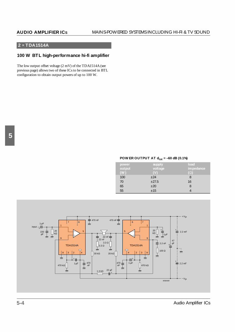
5-4 Audio Amplifier ICs
5
AUDIO AMPLIFIER ICS
2 × TDA1514A
100 W BTL high-performance hi-fi amplifier
The low output offset voltage (2 mV) of the TDA1514A (seeprevious page) allows two of these ICs to be connected in BTLconfiguration to obtain output powers of up to 100 W.
POWER OUTPUT AT dtot = –60 dB (0.1%)
power supply load output voltage impedance(W) (V) (Ω)100 ±24 870 ±27.5 1665 ±20 855 ±15 4
MSB409
VP
22 nF
3.3 Ω
VP
47µF
2.2 mF
2.2 mF
1
9
20kΩ
220pF
input1 µF
TDA1514A
470 kΩ1 µF
8 3 2 4
470nF
67
5
470 nF
20 kΩ
22 nF
3.3 Ω
20 kΩ
22 µF1.3 kΩ
1
9
TDA1514A
8324
6 7
5
2.2 nF
100 Ω
470 nF
20kΩ
1 µF
470 kΩ1 µF470
nF
MAINS-POWERED SYSTEMS INCLUDING HI-FI & TV SOUND

5-5Audio Amplifier ICs
5
AUDIO AMPLIFIER ICS
TDA1521(Q)/TDA2616(Q) AND TDA1521A/TDA2615
2 × 6 W and 2 × 12 W hi-fi amplifiers
Very few external components required
Input muted during power-on and off (no switch-
on or switch-off clicks). This facility allows opera-
tion via remote control
Fixed voltage gain of 30 dB (±16 V supply 8 Ω load)
for excellent gain balance between channels (with-
in 0.2 dB)
High supply voltage ripple rejection (50 dB at
100 Hz)
Channel separation 70 dB (symmetrical supply)
Meets IEC 268 and DIN 45500 hi-fi specifications
Output protected against short-circuit
Thermal protection
The TDA1521(Q) and TDA1521A, and the TDA2615 andTDA2616(Q) are pin-compatible amplifiers for mains-poweredapplications such as stereo TV sound channels and stereo radio.They can operate from a symmetrical power supply of ±7.5 to±21 V or from an asymmetrical power supply of 15 V to 42 V.The low offset voltage (40 mV) between output and ground alsomakes these amplifiers suitable for BTL applications.
The TDA1521A/TDA1521(Q) are identical to the TDA2615/TDA2616(Q) except for a mute facility at pin 2 and internalfeedback interconnected for both channels to pin 8 on theTDA2615/TDA2616(Q). This implies that the TDA2615 andTDA2616(Q) have a fixed gain (30 dB).
The TDA1521A/TDA2615 come in 9-pin plastic SIL medium-power packages. The TDA1521(Q)/TDA2616(Q) come in 9-pin plastic SIL power packages. The pins are bent to DIL for-mat for the versions with a Q suffix.
POWER OUTPUT AT dtot = 0.5%
power supply load output voltage impedance(W) (V) (Ω)TDA1521(Q)/TDA2616(Q): mono BTL20 * 24 8TDA1521(Q)/TDA2616(Q): stereo2 × 12 ** ±16 82 × 6 ±12 82 × 10 ±12 4TDA1521A/TDA2615: stereo2 × 6 ±12 8
* 26 W at dtot = 10% ** 2 × 15 W at dtot = 10%
MSB406
2
3
7
100 nF680 µF
VP
20 kΩ
9
8
20 kΩ
680 Ω 20 kΩ
6
TDA1521(A)
1
680 Ω 20 kΩ
4
22 nF
8.2 Ω
5
2.2 nF
220 nF
100 µF
input
220 nF
MSB407
2
3
7
100 nF680 µF
VP
20 kΩ
9
8
20 kΩ
680 Ω 20 kΩ
9
TDA1521(A)
1
680 Ω 20 kΩ
4
22 nF
8.2 Ω
5
input 1
220 nF
input 2
220 nF
topin 5
22 nF
8.2 Ω
680 µF
VP
MLA940 - 1
100nF
220µF
PV
4
TDA2615TDA2616
3
7
1
5
680 Ω 20 kΩ
R = 8 ΩL
22nF
680µF 20 kΩ
20 kΩ
internal1/2 V P
9
8
680 Ω 20 kΩ
8.2Ω
22nF
680µF
8.2Ω
220 nF
µF
V I
220 nF
V I
2
6
mute input
R = 8 ΩL
100
TDA1521(A) in BTL mono configuration
TDA1521(A) in single-ended stereo configuration
TDA2615/TDA2616 in single-ended stereo configuration
MAINS-POWERED SYSTEMS INCLUDING HI-FI & TV SOUND

5-6 Audio Amplifier ICs
5
AUDIO AMPLIFIER ICS
TDA2611A
4 W to 10 W amplifier
Few external components
Thermal protection
Well defined open-loop gain with simple quiescent
current setting and fixed closed-loop voltage gain
of 38 dB (18 V supply, 8 Ω load)
This amplifier is ideal for the sound output stage of TV sets. Itcan operate from supply voltages between 6 V and 35 V andcomes in a 9-pin plastic SIL medium-power package.
POWER OUTPUT AT dtot = 10%
power supply load output voltage impedance(W) (V) (Ω)4.5 18 810 35 16
MSB415
input 1
330 nF
100 nF
3.3 Ω
330 µF1
100 nFVP
TDA2611A220 pF2
7
6
8
4
22µF
TDA2613/TDA2614
6 W hi-fi amplifiers
Very few external components required
Input muted during power-on and off (no switch-
on or switch-off clicks)
Low offset voltage between output and ground
Meets IEC 268 and DIN 45500 hi-fi specifications
Output protected against short-circuit
Thermal protection
Fixed closed-loop voltage gain of 30 dB (24 V
supply, 8 Ω load)
These are mono versions of the TDA1521A/TDA2615 and arepin compatible with one channel of those ICs. They deliver 6 Wfor mains-powered equipment such as TV sets and radios. Theycan operate from an asymmetrical power supply of between 15and 42 V or from a symmetrical power supply of between ±7.5 V and ±21 V.
The TDA2613 and TDA2614 are identical except for the mutefacility at pin 2 on the TDA2614.
They come in a 9-pin plastic SIL medium-power package.
POWER OUTPUT AT dtot = 0.5%
power supply load output voltage impedance(W) (V) (Ω)6 24 86 ±12 810 24 410 ±12 4
MSB414
VP
input220 nF
9
20 kΩ
TDA2613TDA2614
8.2 Ω
680µF
8
680 Ω
20kΩ
6
5
100nF
7
22nF
23
n.c. (1)
1 4
n.c. n.c.
680µF
100µF
to internal 1/2 VP
MSB413
VP
input220 nF
9
20 kΩ
TDA2613TDA2614
8.2 Ω
680 µF
8
680 Ω
20 k Ω
6
5
100nF
7
680 µF
VP
22 nF
23
n.c. (1)
1 4
n.c. n.c.
TDA2613/TDA2614 with asymmetrical power supply (pin 2 connected for external mute on the TDA2614)
TDA2613/TDA2614 with symmetrical power supply
MAINS-POWERED SYSTEMS INCLUDING HI-FI & TV SOUND

A-1Audio Amplifier ICs
A
APPENDICESAPPENDICES

A-2 Audio Amplifier ICs
A
DataData on our semiconductors for radio/audio systems are avail-able in loose data sheets or are given in Philips Semiconductorsdata handbook IC01a (ordering code 9398 183 00011) andIC01b (ordering code 9398 183 10011).
Data for our semiconductors for TV and video systems are avail-able in loose data sheets or a given in Philips Semiconductorsdata handbooks IC02a (ordering code 9398 652 23011), IC02b(ordering code 9398 652 24011) and IC02c (ordering code 9398 652 24011).
Application Notes and LeafletsThe following Philips Semiconductors Application Notes relat-ing to audio amplifiers are available:
1. “TDA1013B Audio amplifier with DC volume control”Philips Semiconductors Application Note NBA/AN9005.
2. “Recorder IC TDA1016 for portable applications” PhilipsSemiconductors Application Note NBA8301.
3. “TDA1514A Hi-fi power amplifiers” Philips SemiconductorsApplication Note NBA/AN8911.
4. “Audio power ICs for car radios” Philips SemiconductorsApplication Note NBA9001 (ordering code: 9398 07830011).
5. “TDA1551Q, TDA1554Q, TDA1555Q and TDA1558Qaudio power amplifiers for car radio” Philips SemiconductorsApplication Note NBA/AN9202.
6. “TDA1552Q/53(A)Q, TDA1556Q and TDA1557Q doubleBTL amplifiers” Philips Semiconductors Application NoteNBA/AN9013.
7. “TDA1556Q 2 × 22 W BTL amplifier with differentialinputs” Philips Semiconductors Leaflet.
8. “Economic 6 W hi-fi audio amplifier for mains-fed applica-tions” Philips Semiconductors Application Note NBA/AN8902.
9. “TDA2614: economic 6.5 W hi-fi audio amplifier for mains-fed applications” Philips Semiconductors Application NoteNBA/AN9109.
APPENDICES
FURTHER INFORMATION
10. “6.5 W stereo hi-fi audio amplifier for mains-fed applica-tions” Philips Semiconductors Application NoteNBA/AN9110.
11. “12 W stereo hi-fi audio amplifier (20 W BTL)” PhilipsSemiconductors Application Note NBA/AN9205.
12. “TDA7052A; 1 W BTL mono audio amplifier with DC vol-ume control” Philips Semiconductors Application NoteNBA/AN9207.
13. “TDA7052/7053: 1 W componentless BTL mono/stereoaudio amplifiers” Philips Semiconductors Application NoteNBA8907 (ordering code: 9398 068 10011).
14. “TDA7056A; 3 W BTL mono audio amplifier with DC volume control” Philips Semiconductors Application NoteNBA/AN9208.
15. “3 W mono BTL audio amplifier” Philips SemiconductorsApplication Note NBA/AN9009.
16. “TDA7057 3 W componentless BTL stereo audio amplifier”Philips Semiconductors Application Note NBA/AN9009.
17. “TDA1560Q power lifting amplifier (class-H)” PhilipsSemiconductors Application Note NBA/AN9206.
For data sheets/handbooks and Application Notes, please con-tact your local Philips Semiconductors sales organization at theaddress listed on the back cover.
APPENDIX 1
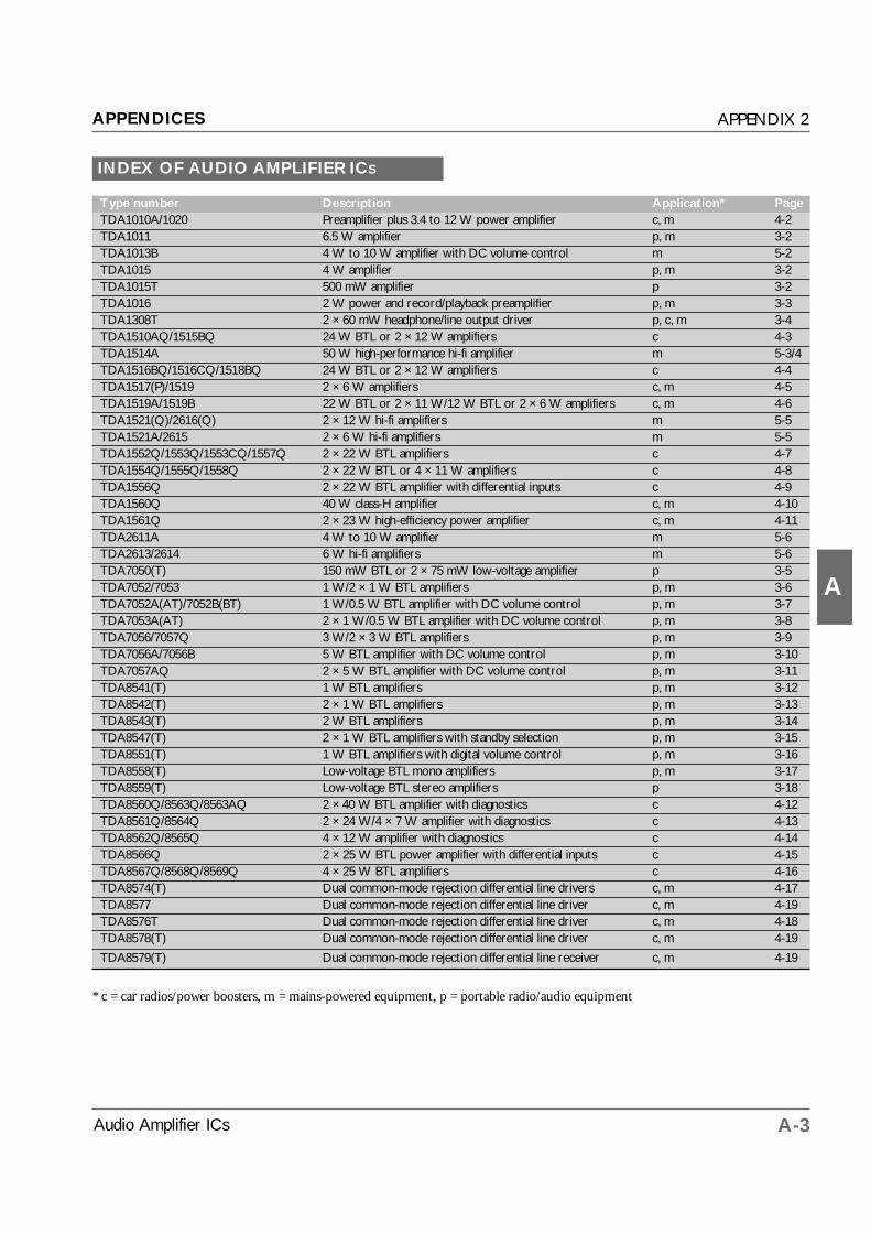
A-3Audio Amplifier ICs
A
INDEX OF AUDIO AMPLIFIER ICS
APPENDICES
Type number Description Application* PageTDA1010A/1020 Preamplifier plus 3.4 to 12 W power amplifier c, m 4-2TDA1011 6.5 W amplifier p, m 3-2TDA1013B 4 W to 10 W amplifier with DC volume control m 5-2TDA1015 4 W amplifier p, m 3-2TDA1015T 500 mW amplifier p 3-2TDA1016 2 W power and record/playback preamplifier p, m 3-3TDA1308T 2 × 60 mW headphone/line output driver p, c, m 3-4TDA1510AQ/1515BQ 24 W BTL or 2 × 12 W amplifiers c 4-3TDA1514A 50 W high-performance hi-fi amplifier m 5-3/4TDA1516BQ/1516CQ/1518BQ 24 W BTL or 2 × 12 W amplifiers c 4-4TDA1517(P)/1519 2 × 6 W amplifiers c, m 4-5TDA1519A/1519B 22 W BTL or 2 × 11 W/12 W BTL or 2 × 6 W amplifiers c, m 4-6TDA1521(Q)/2616(Q) 2 × 12 W hi-fi amplifiers m 5-5TDA1521A/2615 2 × 6 W hi-fi amplifiers m 5-5TDA1552Q/1553Q/1553CQ/1557Q 2 × 22 W BTL amplifiers c 4-7TDA1554Q/1555Q/1558Q 2 × 22 W BTL or 4 × 11 W amplifiers c 4-8TDA1556Q 2 × 22 W BTL amplifier with differential inputs c 4-9TDA1560Q 40 W class-H amplifier c, m 4-10TDA1561Q 2 × 23 W high-efficiency power amplifier c, m 4-11TDA2611A 4 W to 10 W amplifier m 5-6TDA2613/2614 6 W hi-fi amplifiers m 5-6TDA7050(T) 150 mW BTL or 2 × 75 mW low-voltage amplifier p 3-5TDA7052/7053 1 W/2 × 1 W BTL amplifiers p, m 3-6TDA7052A(AT)/7052B(BT) 1 W/0.5 W BTL amplifier with DC volume control p, m 3-7TDA7053A(AT) 2 × 1 W/0.5 W BTL amplifier with DC volume control p, m 3-8TDA7056/7057Q 3 W/2 × 3 W BTL amplifiers p, m 3-9TDA7056A/7056B 5 W BTL amplifier with DC volume control p, m 3-10TDA7057AQ 2 × 5 W BTL amplifier with DC volume control p, m 3-11TDA8541(T) 1 W BTL amplifiers p, m 3-12TDA8542(T) 2 × 1 W BTL amplifiers p, m 3-13TDA8543(T) 2 W BTL amplifiers p, m 3-14TDA8547(T) 2 × 1 W BTL amplifiers with standby selection p, m 3-15TDA8551(T) 1 W BTL amplifiers with digital volume control p, m 3-16TDA8558(T) Low-voltage BTL mono amplifiers p, m 3-17TDA8559(T) Low-voltage BTL stereo amplifiers p 3-18TDA8560Q/8563Q/8563AQ 2 × 40 W BTL amplifier with diagnostics c 4-12TDA8561Q/8564Q 2 × 24 W/4 × 7 W amplifier with diagnostics c 4-13TDA8562Q/8565Q 4 × 12 W amplifier with diagnostics c 4-14TDA8566Q 2 × 25 W BTL power amplifier with differential inputs c 4-15TDA8567Q/8568Q/8569Q 4 × 25 W BTL amplifiers c 4-16TDA8574(T) Dual common-mode rejection differential line drivers c, m 4-17TDA8577 Dual common-mode rejection differential line driver c, m 4-19TDA8576T Dual common-mode rejection differential line driver c, m 4-18TDA8578(T) Dual common-mode rejection differential line driver c, m 4-19
TDA8579(T) Dual common-mode rejection differential line receiver c, m 4-19
* c = car radios/power boosters, m = mains-powered equipment, p = portable radio/audio equipment
APPENDIX 2