Atomic-Scale Characterization of Oxide Thin Films Gated...
24
Subscriber access provided by Drexel University Libraries ACS Applied Materials & Interfaces is published by the American Chemical Society. 1155 Sixteenth Street N.W., Washington, DC 20036 Published by American Chemical Society. Copyright © American Chemical Society. However, no copyright claim is made to original U.S. Government works, or works produced by employees of any Commonwealth realm Crown government in the course of their duties. Article Atomic-Scale Characterization of Oxide Thin Films Gated by Ionic Liquid Andrew Charles Lang, Jennifer D Sloppy, Hessam Ghassemi, Robert C Devlin, Rebecca J Sichel-Tissot, Juan Carlos Idrobo, Steven J. May, and Mitra L. Taheri ACS Appl. Mater. Interfaces, Just Accepted Manuscript • DOI: 10.1021/am504547b • Publication Date (Web): 04 Sep 2014 Downloaded from http://pubs.acs.org on September 11, 2014 Just Accepted “Just Accepted” manuscripts have been peer-reviewed and accepted for publication. They are posted online prior to technical editing, formatting for publication and author proofing. The American Chemical Society provides “Just Accepted” as a free service to the research community to expedite the dissemination of scientific material as soon as possible after acceptance. “Just Accepted” manuscripts appear in full in PDF format accompanied by an HTML abstract. “Just Accepted” manuscripts have been fully peer reviewed, but should not be considered the official version of record. They are accessible to all readers and citable by the Digital Object Identifier (DOI®). “Just Accepted” is an optional service offered to authors. Therefore, the “Just Accepted” Web site may not include all articles that will be published in the journal. After a manuscript is technically edited and formatted, it will be removed from the “Just Accepted” Web site and published as an ASAP article. Note that technical editing may introduce minor changes to the manuscript text and/or graphics which could affect content, and all legal disclaimers and ethical guidelines that apply to the journal pertain. ACS cannot be held responsible for errors or consequences arising from the use of information contained in these “Just Accepted” manuscripts.
Transcript of Atomic-Scale Characterization of Oxide Thin Films Gated...

Subscriber access provided by Drexel University Libraries
ACS Applied Materials & Interfaces is published by the American Chemical Society.1155 Sixteenth Street N.W., Washington, DC 20036Published by American Chemical Society. Copyright © American Chemical Society.However, no copyright claim is made to original U.S. Government works, or worksproduced by employees of any Commonwealth realm Crown government in the courseof their duties.
Article
Atomic-Scale Characterization of Oxide Thin Films Gated by Ionic LiquidAndrew Charles Lang, Jennifer D Sloppy, Hessam Ghassemi, Robert C Devlin,
Rebecca J Sichel-Tissot, Juan Carlos Idrobo, Steven J. May, and Mitra L. TaheriACS Appl. Mater. Interfaces, Just Accepted Manuscript • DOI: 10.1021/am504547b • Publication Date (Web): 04 Sep 2014
Downloaded from http://pubs.acs.org on September 11, 2014
Just Accepted
“Just Accepted” manuscripts have been peer-reviewed and accepted for publication. They are postedonline prior to technical editing, formatting for publication and author proofing. The American ChemicalSociety provides “Just Accepted” as a free service to the research community to expedite thedissemination of scientific material as soon as possible after acceptance. “Just Accepted” manuscriptsappear in full in PDF format accompanied by an HTML abstract. “Just Accepted” manuscripts have beenfully peer reviewed, but should not be considered the official version of record. They are accessible to allreaders and citable by the Digital Object Identifier (DOI®). “Just Accepted” is an optional service offeredto authors. Therefore, the “Just Accepted” Web site may not include all articles that will be publishedin the journal. After a manuscript is technically edited and formatted, it will be removed from the “JustAccepted” Web site and published as an ASAP article. Note that technical editing may introduce minorchanges to the manuscript text and/or graphics which could affect content, and all legal disclaimersand ethical guidelines that apply to the journal pertain. ACS cannot be held responsible for errorsor consequences arising from the use of information contained in these “Just Accepted” manuscripts.

1
Atomic-Scale Characterization of Oxide Thin Films
Gated by Ionic Liquid
Andrew C. Lang1, Jennifer D. Sloppy
1, Hessam Ghassemi
1, Robert C. Devlin
1, Rebecca J. Sichel-
Tissot1, Juan-Carlos Idrobo
2, Steven J. May
1, and Mitra L. Taheri
1*
1. Department of Materials Science and Engineering, Drexel University, Philadelphia,
Pennsylvania, United States.
2. Center for Nanophase Materials Sciences Division, Oak Ridge National Laboratory, Oak
Ridge, Tennessee, United States.
Keywords: La1/3Sr2/3FeO3, ionic liquid gating, transmission electron microscopy, charge
accumulation, electron energy loss spectroscopy, oxide thin film
Abstract
Ionic liquids (ILs) have received considerable interest for use in electrostatic gating in complex
oxide systems. Understanding the ionic liquid/oxide interface, and any bias-induced
electrochemical degradation, is critical for the interpretation of transport phenomena. The
integrity of the interface between ionic liquid 1-ethyl-3-methylimidazolium hexafluorophosphate
and La1/3Sr2/3FeO3 under various biasing conditions was examined by analytical transmission
electron microscopy, and we report film degradation in the form of an irreversible chemical
reaction regardless of the applied bias. This results in an intermixing region of 4-6 nm at the
Page 1 of 23
ACS Paragon Plus Environment
ACS Applied Materials & Interfaces
123456789101112131415161718192021222324252627282930313233343536373839404142434445464748495051525354555657585960

2
IL/oxide interface. Electron energy loss spectroscopy shows La and Fe migration into the ionic
liquid, resulting in secondary phase formation under negative bias. Our approach can be
extended to other ionic liquid/oxide systems in order to better understand the electrochemical
stability window of these device structures.
Introduction
Materials that experience electronic phase transitions, such as metal-insulator transitions or
semiconducting-superconducting transitions, are excellent candidates for electronic devices like
field-effect transistors.1–4
Such devices require that switching between conductive and insulating
states be achieved by an applied bias.2,5
The use of conventional dielectrics for electrostatic
carrier doping, and the limitations imposed by dielectric breakdown, are often an impeding factor
in field-effect based control of metal-insulator phase transitions.1,6
Ionic Liquids (ILs) have been shown to be an innovative means of inducing and maintaining
charge accumulation, that can be orders of magnitude larger than that achieved with solid
dielectrics.7–13
ILs are binary salts that are chemically and thermally stable when heated above
their melting temperatures; they are highly polar, have low-melting temperatures and do not
require solvents.7 Charge accumulation occurs via an applied bias to the IL, which separates
ions within the IL and forms an electric-double-layer (EDL) on the ends of the electrodes. The
EDL is a densely packed layer of ions, separated from the channel material by approximately
1nm, which generates extremely high capacitance (up to 10 μF9) and can induce a sheet carrier
density on the order of 1014
cm-2
within the adjacent channel material.10,12
These properties have
fueled much research related to the use of ILs as liquid gate dielectrics; 11,14–19
however, recent
research has revealed some limitations of using ILs as a biasing medium due various
electrochemical effects.6,10,12,15,20–22
In the case of NdNiO3, while reversible charge
Page 2 of 23
ACS Paragon Plus Environment
ACS Applied Materials & Interfaces
123456789101112131415161718192021222324252627282930313233343536373839404142434445464748495051525354555657585960

3
accumulation was achieved at biases between 0 and -2.5 V, a large irreversible change in
electronic transport behavior was observed when NdNiO3 thin films were gated with VG < -2.5V,
which indicated operation outside of a safe electrochemical window.12
In SrTiO3 EDL-
transistors, it was found that electrochemical reactions dominate the change in electronic
transport behavior observed when IL is biased greater than 3.75 V and that changes in oxygen
stoichiometry may be at fault.6,10,20
Additionally, the electrical changes induced by IL-gating of
VO2 EDL-transistors has also been attributed to electrochemical effects.21,23
Typically, it is
postulated that there exists a distinct energy barrier above which an applied bias will cause an
irreversible electrochemical reaction between an IL and an oxide thin film. Presumably the
voltage threshold for electrochemical reactions depends on the compositional and structural
specifics of the ionic liquid and oxide materials investigated; as such, accessible techniques that
probe the integrity of the oxide film, at the atomic scale, during ionic liquid gating can provide
tremendous benefit in elucidating the role of electrostatics and electrochemistry in field-effect
induced electronic transport behavior.
To date, several studies have employed atomic force microscopy as a means to probe the
IL/solid interface.24–26
While they have successfully imaged IL/solid interfaces and revealed the
local arrangement of IL molecules, their findings are hindered by the high viscosity of ILs24
and
the need to image parallel to the IL/solid interface in plan-view. In this work, we report the
direct observation of IL/oxide thin film interfaces, in cross-section, under bias using
conventional and analytical transmission electron microscopy techniques. Specifically, the
structural and chemical changes of IL/La1/3Sr2/3FeO3 (LSFO) junctions are examined as a
function of bias using high resolution imaging coupled with electron energy loss spectroscopy
(EELS) in aberration-corrected scanning transmission electron microscopy (STEM). LSFO is a
Page 3 of 23
ACS Paragon Plus Environment
ACS Applied Materials & Interfaces
123456789101112131415161718192021222324252627282930313233343536373839404142434445464748495051525354555657585960

4
correlated oxide material that experiences a charge-ordering phase transition at 190 K and is of
much research interest to those wishing to understand and control metal-insulator transitions in
correlated oxides.22,27
Specific to the material system investigated herein, we provide evidence
that an irreversible chemical reaction occurs regardless of the applied bias, resulting in an
intermixing region of 4-6 nm at the IL/oxide interface.
Experimental Procedure
Materials and Film Growth. LSFO thin films were grown via molecular beam epitaxy on
(001)-oriented SrTiO3 substrates, followed by a post-growth 200 °C anneal in a mixture of dilute
ozone in oxygen at atmospheric pressure in order to minimize the concentration of oxygen
vacancies in the film.28
The IL used in this study, 1-Ethyl-3-Methylimidazolium
Hexafluorophosphate obtained from Ionic Liquids Technologies, Inc., was chosen for its melting
point of ~ 60 °C, which ensures a solid state of the electrolyte at room temperature for the
electron microscopy measurements. Note that this melting temperature is substantially higher
than that of commonly used ILs in oxide gating experiments such as EMI-TFSI, DEME-BF4 and
DEME-TFSI.29
Electric-Double-Layer Formation. A 10 x 10 mm LSFO film was sectioned into four
different samples: a control with no IL and no bias (0 V), and three samples with IL: 0 V, -1 V
and -2 V bias. These bias conditions were chosen to cover the representative range of applied
voltages found in literature.10,12
All samples examined came from this single film growth to
ensure consistency among the starting film conditions. The experiment proceeded as follows: a
droplet of IL was heated to its melting temperature of approximately 60ºC and was placed on an
unheated LSFO film. The film and IL were then heated above the IL melting temperature
allowing for a gold wire electrode to be dipped into the IL and biased at the conditions
Page 4 of 23
ACS Paragon Plus Environment
ACS Applied Materials & Interfaces
123456789101112131415161718192021222324252627282930313233343536373839404142434445464748495051525354555657585960

5
previously outlined. The heat was then removed from the IL and film, while maintaining the
bias, to allow the IL to solidify and freeze in the ionic arrangement.
Characterization. Electron transparent TEM samples were prepared via mechanical milling,
followed by a conventional in-situ lift-out procedure30
using a FEI Strata DB 235 dual beam
focused ion beam-scanning electron microscope. Bright field-TEM imaging was performed in a
JEOL 2100 LaB6 TEM operated at 200 kV. STEM imaging and EELS experiments were
performed using an aberration corrected Nion UltraSTEMTM
100 operating at 100 kV,31
which
is equipped with a Gatan Enfina spectrometer. EEL spectra were processed with a power law
background subtraction. EEL edge intensity maps were produced by integrating over a 40 eV
window starting from the first peak of each edge reported. The peak positions from EELS, when
reported, were obtained by fitting a Gaussian distribution to the spectra to find the peak maxima.
Results and Discussion
High Resolution TEM Analysis. Conventional TEM analyses of the negatively biased
IL/oxide films revealed different IL/oxide interfaces depending on the applied bias. High
resolution BF-TEM images of the four LSFO samples (sectioned from the same film thus
possessing the same initial composition and structure) are shown in Figure 1. Image analysis
determined a LSFO film thickness of 18.5 ± 0.5 nm for the control, Figure 1a, 17 ± 1 nm for the
0 V sample, Figure 1b, 15 ± 2 nm for the -1 V bias sample, Figure 1c, and 17 ± 3 nm for the -2 V
bias sample, Figure 1d. Our measured thickness values only consider the crystalline LSFO as
the film. In a direct comparison to the control sample, the presence of IL alone degraded the
LSFO film by 1.5 ± 1 nm. In addition, there was increased LSFO film roughness present
between the control and 0 V samples, suggesting that the presence of this IL on LSFO resulted in
an interfacial reaction. Furthermore, in both the -1 V and -2 V samples, there was a clear
Page 5 of 23
ACS Paragon Plus Environment
ACS Applied Materials & Interfaces
123456789101112131415161718192021222324252627282930313233343536373839404142434445464748495051525354555657585960

6
electrochemical degradation of the LSFO thin film. A ~ 2 nm thick secondary phase was present
over approximately 70% of LSFO film surface in the -1 V sample. Lastly, the entire surface of
the -2 V sample was degraded with over half of the LSFO film volume damaged below the
original IL/film interface. In all samples analyzed, the oxide film appears to have been altered
by the presence of IL.
Z-contrast Imaging. High angle annular dark field STEM images (also known as Z-Contrast
images)32
of the 0 V and -1 V films, shown in Figure 2, reveal an intermixing region at the
IL/oxide interface. The most prominent feature of these images was the atomic number contrast
found near the IL/LSFO interface. Neither the 0 V nor the -1 V samples contain an abrupt
IL/LSFO interface; the STEM images suggest the IL/LSFO interface is within an intermixing
region that has a thickness of 4-6 nm. In regions away from the interface, the LSFO film in the 0
V sample, Figure 2a, appeared to be unaffected by the IL, while the -1 V sample, Figure 2b,
contained streaks of contrast that indicated the presence of aligned oxygen vacancies within the
LSFO film.33
Analysis of the fast Fourier transform (FFT) indicated that the phase found in the
intermixing region of the -1 V sample indexed to a hexagonal structure consistent with the lattice
spacing of (111)-oriented La2O3.34
Electron Energy Loss Spectroscopy. EELS analysis of both the 0 V and -1 V samples
revealed significant changes in the O K-, Fe L- and La M-edges of both samples, which indicated
intermixing of the IL and LSFO film in the interfacial region. A depth-resolved EELS edge
intensity plot from the 0 V sample, shown in Figure 3a, indicated that both La and Fe were
present within the IL several nm away from the film. The intermixing region between the IL and
the LSFO was largely composed of La, which was the reason for the increased atomic number
contrast observed in the HAADF images of the interfacial region. Furthermore, the composition
Page 6 of 23
ACS Paragon Plus Environment
ACS Applied Materials & Interfaces
123456789101112131415161718192021222324252627282930313233343536373839404142434445464748495051525354555657585960

7
of the LSFO film varied across the first 5 unit cells, decreasing in La content and increasing in
Fe content, before it achieved consistency with the rest of the film.
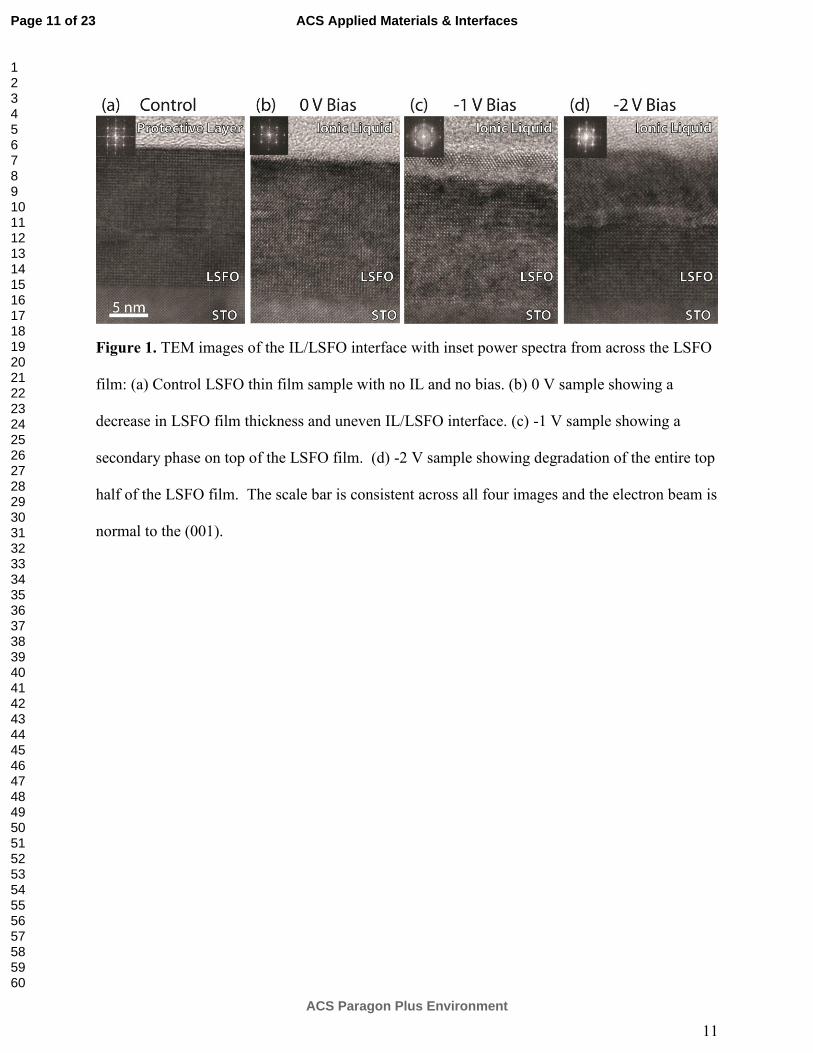
Extracted core loss spectra chosen from specific areas of the IL/LSFO interface of the 0 V
sample are shown in Figure 4a and b. The Fe L3,2 near-edge fine structure, shown in Figure 4a,
experiences a 1.1 ± 0.4 eV shift to higher energy upon crossing the IL/LSFO interface and
moving into the LSFO film. The Fe L-edge in the IL and intermixing region exhibited a L3 peak
at 707.6 eV, which shifted to 708.7 eV five unit cells into the film; this is indicative of Fe
valence being in a mixed 2+/3
+ state in the IL and intermixing region and in a mixed 3
+/4
+ state
within the LSFO film.35
The Fe valence found within the LSFO film was consistent with past
literature on the nominal valence of Fe in LSFO, which was reported to be nominally Fe3.67+
. 36,37
The O K-edge, shown in Figure 4b, consists of a single main peak in the IL and intermixing
region, then develops a pre-peak in the film, which indicates hybridization between O 2p and Fe
3d orbitals,38
and after five unit cells into the film the O K-edge splits into two separate peaks
and remains this way throughout the rest of the film.
The depth-resolved edge intensity plot from the -1 V sample, shown in Figure 3b, exhibited
strikingly different features compared to the 0 V sample. The EELS data indicates no significant
concentration of La and Fe in the IL, but revealed that the intermixing region consists of two
compositionally different parts. The secondary phase, indexed previously to La2O3, consists of
predominantly of La, with minimal Fe, and a small amount of F from the IL. The incorporation
of F, from the hexafluorophosphate anion, within the La2O3 layer strongly indicates
electrochemical degradation. The area immediately below the secondary phase exhibits a high
Fe and O concentration and slightly depleted La concentration. Below the Fe rich region, the
Page 7 of 23
ACS Paragon Plus Environment
ACS Applied Materials & Interfaces
123456789101112131415161718192021222324252627282930313233343536373839404142434445464748495051525354555657585960

8
film exhibits consistent edge intensities indicating little fluctuation in film composition outside
of the first few unit cells.
Extracted core loss spectra chosen from specific areas of the IL/LSFO interface of the -1 V
sample are shown in Figure 4c and d. The Fe L3,2 near-edge structure, shown in Figure 4c,
revealed no significant shift of the Fe L3 edge across the entire intermixing region. The Fe L3
peak was located at 708.8 eV and was similar to the one seen in the 0 V LSFO film, indicative of
a mixed 3+/4
+ Fe valence state throughout the interfacial region and the LSFO film. The absence
of any Fe valence shift suggested that there is no evidence for charge accumulation in this
sample. The O K-edge, shown in Figure 4d, consisted of a single peak in the IL, and then
develops a pre-peak feature at the bottom of the secondary phase, which increases linearly with
Fe L3 intensity throughout the intermixing region. The O K-edge spectra taken from the Fe and
O rich area contains a well-defined pre-peak and appears to be chemically shifted slightly to
higher energies. The shape of the O K-edge is very similar to that observed from Fe2O3,
suggesting that this region may consist of iron oxide.35
When moving into the film the O K-edge
splits into two separate peaks after five unit cells and began to resemble the O K-edge of the 0 V
sample.
Conclusions
The results from these measurements suggest two main points: (1) chemical intermixing
occurred, over a 4-6 nm intermixing region, between the IL and LSFO thin film even in the
absence of an applied bias and (2) the application of bias further degraded the LSFO thin film
resulting in the formation of two compositionally different layers in the intermixing region. We
rule out the possibility of FIB induced damage because the vacuum surface edge of the sample,
which is normal to the ion beam during preparation and is prone to amorphization and ion-
Page 8 of 23
ACS Paragon Plus Environment
ACS Applied Materials & Interfaces
123456789101112131415161718192021222324252627282930313233343536373839404142434445464748495051525354555657585960

9
induced damage, is more than 100 nm away from all regions of analysis.39
From Figures 1a and
b it is clear that IL reduced the LSFO film thickness by a few unit-cells compared with the IL-
free control sample. The Z-Contrast images and EELS analysis confirmed the presence of La
and Fe throughout the intermixing region of the 0 V sample. An applied bias of -1 V resulted in
the formation of two compositionally different layers in the intermixing region, shown in Figure
3b. The most striking feature of the -1 V sample was the crystalline layer at the top of the
intermixing region which structurally and chemically appears to be La2O3. The small amount of
anion incorporation observed in the La2O3 further suggests electrochemical degradation.
Although the electronic transport properties of these films were not measured, the formation of
La2O3, an insulator with a high dielectric constant,40
would undoubtedly change the electrical
properties of the IL/LSFO interface. The formation of this phase clearly indicates the presence
of an electrochemical reaction, such as that seen during operation outside of the electrochemical
stability window in this specific system.
While the transfer characteristics of an EDL-transistor system are subject to an electrochemical
stability window it is unclear whether that statement extends to the structure of the IL/oxide thin
film interface present in the system. Directly comparing with the previous studies mentioned
employing NdNiO3, SrTiO3, and VO2, they report no degradation due the chemical interaction
between their IL and thin films at 0 V bias.6,10,12,20,21,23
These results suggest that the IL observed
here may be more reactive than ILs commonly used in field-effect experiments. It is important
to note that, by heating the IL to 60ºC to perform our experiments, we may have an added
thermal effect at the IL/LSFO interface, the possibility of this effect could be examined in future
studies by varying the temperature of the IL droplet when it is placed on the oxide film. We
caution against extrapolating our particular results to other systems. However, this experimental
Page 9 of 23
ACS Paragon Plus Environment
ACS Applied Materials & Interfaces
123456789101112131415161718192021222324252627282930313233343536373839404142434445464748495051525354555657585960

10
methodology can be used with other more common IL/oxide systems, taking advantage of cryo-
based sample preparation and characterization techniques. We anticipate that the approach
demonstrated herein can be applied to interfaces between ionic liquids and a wide variety of
electronic materials, providing researchers with a powerful means to disentangle the complex
physical and electrochemical interactions present at these heterojunctions. It is clear from our
results that coupling high resolution and analytical TEM techniques with traditional EDL-
transistor characterization will allow for a more accurate determination of safe operating
parameters for IL-gated oxide device structures.
Page 10 of 23
ACS Paragon Plus Environment
ACS Applied Materials & Interfaces
123456789101112131415161718192021222324252627282930313233343536373839404142434445464748495051525354555657585960
11
Figure 1. TEM images of the IL/LSFO interface with inset power spectra from across the LSFO
film: (a) Control LSFO thin film sample with no IL and no bias. (b) 0 V sample showing a
decrease in LSFO film thickness and uneven IL/LSFO interface. (c) -1 V sample showing a
secondary phase on top of the LSFO film. (d) -2 V sample showing degradation of the entire top
half of the LSFO film. The scale bar is consistent across all four images and the electron beam is
normal to the (001).
Page 11 of 23
ACS Paragon Plus Environment
ACS Applied Materials & Interfaces
123456789101112131415161718192021222324252627282930313233343536373839404142434445464748495051525354555657585960

12
Figure 2. STEM-HAADF images with inset power spectra from the LSFO film: (a) 0 V sample.
Note the 4-6 nm region of z-contrast above the LSFO film suggesting IL/LSFO intermixing at
the interface. (b) -1 V sample showing a region of z-contrast above the LSFO film similar to (a)
with a secondary polycrystalline phase on top of the film with inset power spectra from the
secondary phase.
Page 12 of 23
ACS Paragon Plus Environment
ACS Applied Materials & Interfaces
123456789101112131415161718192021222324252627282930313233343536373839404142434445464748495051525354555657585960

13
Figure 3. Integrated EELS edge intensity plots across the IL/LSFO interface with corresponding
HAADF images. The x-axis indicates the LSFO film surface, with 0 indicating the surface,
negative values moving into the IL and positive values moving into the LSFO film. (a) 0 V
sample, note the presence of La and Fe in the IL and the high concentration of La in the
intermixing region. The decrease in the O edge intensity within the LSFO film is due to the rise
of a strong pre-peak feature in the spectra. No F was observed in the 0 V sample. (b) -1 V
sample, note the variance in composition of the intermixing region showing two compositionally
distinct phases; the crystalline secondary phase exhibits a high La concentration as well as F
from the IL. The integrated energy range for each spectrum is 40 eV starting from the first peak
of each edge.
Page 13 of 23
ACS Paragon Plus Environment
ACS Applied Materials & Interfaces
123456789101112131415161718192021222324252627282930313233343536373839404142434445464748495051525354555657585960

14
Figure 4. EELS fine structure of the Fe L- and O K-edge; all spectra have been processed with a
power law background subtraction, and shown spectra are row averaged over 1 unit cell. (a) and
(b) are the Fe L- and O K-edges of 0 V sample, the accompanying HAADF image with colored
lines denotes the area where the spectra were taken. (c) and (d) are the Fe L- and O K-edges of
the -1 V sample, the accompanying HAADF image denotes the area where the spectra were
taken. The horizontal shift in the Fe L-edge in (a) is representative of a change in the oxidation
state of Fe across the IL/LSFO interface through the first 5 unit cells of the film.
Page 14 of 23
ACS Paragon Plus Environment
ACS Applied Materials & Interfaces
123456789101112131415161718192021222324252627282930313233343536373839404142434445464748495051525354555657585960

15
AUTHOR INFORMATION
Corresponding Author
* Address correspondence to [email protected] (Mitra L. Taheri)
Conflict of Interest: The authors declare no competing financial interest
ACKNOWLEDGMENT
This work was supported by Office of Naval Research under grant numbers N00014-11-1-0664
and N00014-1101-0296, and through a user project supported by ORNL’s Center for Nanophase
Materials Sciences (CNMS), which is sponsored by the Scientific User Facilities Division,
Office of Basic Energy Sciences, U.S. Department of Energy (JCI).
REFERENCES
(1) Ahn, C. H.; Triscone, J.-M.; Mannhart, J. Electric Field Effect in Correlated Oxide
Systems. Nature 2003, 424, 1015–1018.
(2) Dawber, M.; Scott, J. F. Physics of Thin-Film Ferroelectric Oxides. Rev. Mod. Phys. 2005,
77, 1083–1130.
(3) Prabhumirashi, P.; Dravid, V. P.; Lupini, A. R.; Chisholm, M. F.; Pennycook, S. J.
Atomic-Scale Manipulation of Potential Barriers at SrTiO3 Grain Boundaries. Appl. Phys.
Lett. 2005, 87, 121917.
(4) Takagi, H.; Hwang, H. Y. An Emergent Change of Phase for Electronics. Science 2010,
327, 1601–1602.
(5) Ahn, C. H.; Di Ventra, M.; Eckstein, J. N.; Frisbie, C. D.; Gershenson, M. E.; Goldman,
A. M.; Inoue, I. H.; Mannhart, J.; Millis, A. J.; Morpurgo, A. F.; Natelson, D.; Triscone, J.
-M. Electrostatic Modification of Novel Materials. Rev. Mod. Phys. 2006, 78, 1185–1212.
(6) Ueno, K.; Nakamura, S.; Shimotani, H.; Ohtomo, A.; Kimura, N.; Nojima, T.; Aoki, H.;
Iwasa, Y.; Kawasaki, M. Electric-Field-Induced Superconductivity in an Insulator. Nat.
Mater. 2008, 7, 855–858.
Page 15 of 23
ACS Paragon Plus Environment
ACS Applied Materials & Interfaces
123456789101112131415161718192021222324252627282930313233343536373839404142434445464748495051525354555657585960

16
(7) Galiński, M.; Lewandowski, A.; Stępniak, I. Ionic Liquids as Electrolytes. Electrochim.
Acta 2006, 51, 5567–5580.
(8) Misra, R.; McCarthy, M.; Hebard, A. F. Electric Field Gating with Ionic Liquids. Appl.
Phys. Lett. 2007, 90, 052905.
(9) Ye, J. T.; Zhang, Y. J.; Akashi, R.; Bahramy, M. S.; Arita, R.; Iwasa, Y. Superconducting
Dome in a Gate-Tuned Band Insulator. Science 2012, 338, 1193–1196.
(10) Ueno, K.; Shimotani, H.; Iwasa, Y.; Kawasaki, M. Electrostatic Charge Accumulation
versus Electrochemical Doping in SrTiO3 Electric Double Layer Transistors. Appl. Phys.
Lett. 2010, 96, 252107.
(11) Ye, J. T.; Inoue, S.; Kobayashi, K.; Kasahara, Y.; Yuan, H. T.; Shimotani, H.; Iwasa, Y.
Liquid-Gated Interface Superconductivity on an Atomically Flat Film. Nat. Mater. 2010,
9, 125–128.
(12) Asanuma, S.; Xiang, P.-H.; Yamada, H.; Sato, H.; Inoue, I. H.; Akoh, H.; Sawa, A.; Ueno,
K.; Shimotani, H.; Yuan, H.; Kawasaki, M.; Iwasa, Y. Tuning of the Metal-Insulator
Transition in Electrolyte-Gated NdNiO3 Thin Films. Appl. Phys. Lett. 2010, 97, 142110.
(13) Nakano, M.; Shibuya, K.; Okuyama, D.; Hatano, T.; Ono, S.; Kawasaki, M.; Iwasa, Y.;
Tokura, Y. Collective Bulk Carrier Delocalization Driven by Electrostatic Surface Charge
Accumulation. Nature 2012, 487, 459–462.
(14) Dhoot, A.; Israel, C.; Moya, X.; Mathur, N.; Friend, R. Large Electric Field Effect in
Electrolyte-Gated Manganites. Phys. Rev. Lett. 2009, 102, 136402.
(15) Ji, H.; Wei, J.; Natelson, D. Modulation of the Electrical Properties of VO2 Nanobeams
Using an Ionic Liquid as a Gating Medium. Nano Lett. 2012, 12, 2988–2992.
(16) Lee, M.; Williams, J. R.; Zhang, S.; Frisbie, C. D.; Goldhaber-Gordon, D. Electrolyte
Gate-Controlled Kondo Effect in SrTiO3. Phys. Rev. Lett. 2011, 107, 256601.
(17) Lee, Y.; Clement, C.; Hellerstedt, J.; Kinney, J.; Kinnischtzke, L.; Leng, X.; Snyder, S.
D.; Goldman, A. M. Phase Diagram of Electrostatically Doped SrTiO3. Phys. Rev. Lett.
2011, 106, 136809.
(18) Scherwitzl, R.; Zubko, P.; Lezama, I. G.; Ono, S.; Morpurgo, A. F.; Catalan, G.; Triscone,
J.-M. Electric-Field Control of the Metal-Insulator Transition in Ultrathin NdNiO3 Films.
Adv. Mater. 2010, 22, 5517–5520.
(19) Liu, K.; Fu, D.; Cao, J.; Suh, J.; Wang, K. X.; Cheng, C.; Ogletree, D. F.; Guo, H.;
Sengupta, S.; Khan, A.; Yeung, C. W.; Salahuddin, S.; Deshmukh, M. M.; Wu, J. Dense
Electron System from Gate-Controlled Surface Metal-Insulator Transition. Nano Lett.
2012, 12, 6272–6277.
Page 16 of 23
ACS Paragon Plus Environment
ACS Applied Materials & Interfaces
123456789101112131415161718192021222324252627282930313233343536373839404142434445464748495051525354555657585960

17
(20) Li, M.; Han, W.; Jiang, X.; Jeong, J.; Samant, M. G.; Parkin, S. S. P. Suppression of Ionic
Liquid Gate-Induced Metallization of SrTiO3(001) by Oxygen. Nano Lett. 2013, 13,
4675–4678.
(21) Jeong, J.; Aetukuri, N.; Graf, T.; Schladt, T. D.; Samant, M. G.; Parkin, S. S. P.
Suppression of Metal-Insulator Transition in VO2 by Electric Field-Induced Oxygen
Vacancy Formation. Science 2013, 339, 1402–1405.
(22) Ma, J.; Yan, J.-Q.; Diallo, S. O.; Stevens, R.; Llobet, A.; Trouw, F.; Abernathy, D. L.;
Stone, M. B.; McQueeney, R. J. Role of Magnetic Exchange Energy on Charge Ordering
in R1/3Sr2/3FeO3 (R=La, Pr, and Nd). Phys. Rev. B 2011, 84, 224115.
(23) Zhou, Y.; Ramanathan, S. Relaxation Dynamics of Ionic liquid—VO2 Interfaces and
Influence in Electric Double-Layer Transistors. J. Appl. Phys. 2012, 111, 084508.
(24) Yokota, Y.; Harada, T.; Fukui, K. Direct Observation of Layered Structures at Ionic
Liquid/solid Interfaces by Using Frequency-Modulation Atomic Force Microscopy. Chem.
Commun. 2010, 46, 8627–8629.
(25) Negami, M.; Ichii, T.; Murase, K.; Sugimura, H. Visualization of Ionic-Liquid/Solid
Interfaces by Frequency Modulation Atomic Force Microscopy. ECS Trans. 2013, 50,
349–355.
(26) Segura, J. J.; Elbourne, A.; Wanless, E. J.; Warr, G. G.; Voïtchovsky, K.; Atkin, R.
Adsorbed and near Surface Structure of Ionic Liquids at a Solid Interface. Phys. Chem.
Chem. Phys. 2013, 15, 3320–3328.
(27) Park, S. K.; Ishikawa, T.; Tokura, Y.; Li, J. Q.; Matsui, Y. Variation of Charge-Ordering
Transitions in R1/3Sr2/3FeO3 (R= La , Pr , Nd , Sm , and Gd). Phys. Rev. B 1999, 60, 788–
795.
(28) Xie, Y.; Scafetta, M. D.; Sichel-Tissot, R. J.; Moon, E. J.; Devlin, R. C.; Wu, H.; Krick,
A. L.; May, S. J. Control of Functional Responses Via Reversible Oxygen Loss in La1-
XSrXFeO3-Δ Films. Adv. Mater. 2014, 26, 1434–1438.
(29) Zhou, Y.; Ramanathan, S. Correlated Electron Materials and Field Effect Transistors for
Logic: A Review. Crit. Rev. Solid State Mater. Sci. 2013, 38, 286–317.
(30) Langford, R. M.; Rogers, M. In Situ Lift-out: Steps to Improve Yield and a Comparison
with Other FIB TEM Sample Preparation Techniques. Micron 2008, 39, 1325–1330.
(31) Krivanek, O. L.; Corbin, G. J.; Dellby, N.; Elston, B. F.; Keyse, R. J.; Murfitt, M. F.;
Own, C. S.; Szilagyi, Z. S.; Woodruff, J. W. An Electron Microscope for the Aberration-
Corrected Era. Ultramicroscopy 2008, 108, 179–195.
Page 17 of 23
ACS Paragon Plus Environment
ACS Applied Materials & Interfaces
123456789101112131415161718192021222324252627282930313233343536373839404142434445464748495051525354555657585960

18
(32) Browning, N. D.; Chisholm, M. F.; Pennycook, S. J. Atomic-Resolution Chemical
Analysis Using a Scanning Transmission Electron Microscope. Nature 1993, 366, 143–
146.
(33) Klie, R. F. Characterization of Oxygen Ordering in (La, Sr)FeO3-δ by Atomic Resolution
Z-Contrast Imaging and Electron Energy-Loss Spectroscopy. J. Electron Microsc.
(Tokyo). 2002, 51, 59S–66.
(34) Wang, C.; Tan, M.; Feng, C.; Ma, Z.; Jiang, S.; Xu, Z.; Cao, G.; Matsubayashi, K.;
Uwatoko, Y. La2Co2Se2O3: A Quasi-Two-Dimensional Mott Insulator with Unusual
Cobalt Spin State and Possible Orbital Ordering. J. Am. Chem. Soc. 2010, 132, 7069–
7073.
(35) Tan, H.; Verbeeck, J.; Abakumov, A.; Van Tendeloo, G. Oxidation State and Chemical
Shift Investigation in Transition Metal Oxides by EELS. Ultramicroscopy 2012, 116, 24–
33.
(36) Takano, M.; Kawachi, J.; Nakanishi, N.; Takeda, Y. Valence State of the Fe Ions in
Sr1−yLayFeO3. J. Solid State Chem. 1981, 39, 75–84.
(37) Battle, P. D.; Gibb, T. C.; Lightfoot, P. The Structural Consequences of Charge
Disproportionation in Mixed-Valence Iron Oxides. I. The Crystal Structure of
Sr2LaFe3O8.94 at Room Temperature and 50 K. J. Solid State Chem. 1990, 84, 271–279.
(38) De Groot, F.; Grioni, M.; Fuggle, J.; Ghijsen, J.; Sawatzky, G.; Petersen, H. Oxygen 1s X-
Ray-Absorption Edges of Transition-Metal Oxides. Phys. Rev. B 1989, 40, 5715–5723.
(39) Giannuzzi, L. A.; Geurts, R.; Ringnalda, J. 2 keV Ga+ FIB Milling for Reducing
Amorphous Damage in Silicon. Microsc. Microanal. 2005, 11, 828–829.
(40) Robertson, J. Interfaces and Defects of High-K Oxides on Silicon. Solid. State. Electron.
2005, 49, 283–293.
Page 18 of 23
ACS Paragon Plus Environment
ACS Applied Materials & Interfaces
123456789101112131415161718192021222324252627282930313233343536373839404142434445464748495051525354555657585960

Figure 1. TEM images of the IL/LSFO interface with inset power spectra from across the LSFO film: (a) Control LSFO thin film sample with no IL and no bias. (b) 0 V sample showing a decrease in LSFO film
thickness and uneven IL/LSFO interface. (c) -1 V sample showing a secondary phase on top of the LSFO
film. (d) -2 V sample showing degradation of the entire top half of the LSFO film. The scale bar is consistent across all four images and the electron beam is normal to the (001).
65x24mm (300 x 300 DPI)
Page 19 of 23
ACS Paragon Plus Environment
ACS Applied Materials & Interfaces
123456789101112131415161718192021222324252627282930313233343536373839404142434445464748495051525354555657585960

Figure 2. STEM-HAADF images with inset power spectra from the LSFO film: (a) 0 V sample. Note the 4-6 nm region of z-contrast above the LSFO film suggesting IL/LSFO intermixing at the interface. (b) -1 V
sample showing a region of z-contrast above the LSFO film similar to (a) with a secondary polycrystalline
phase on top of the film with inset power spectra from the secondary phase. 95x51mm (300 x 300 DPI)
Page 20 of 23
ACS Paragon Plus Environment
ACS Applied Materials & Interfaces
123456789101112131415161718192021222324252627282930313233343536373839404142434445464748495051525354555657585960

Figure 3. Integrated EELS edge intensity plots across the IL/LSFO interface with corresponding HAADF images. The x-axis indicates the LSFO film surface, with 0 indicating the surface, negative values moving into the IL and positive values moving into the LSFO film. (a) 0 V sample, note the presence of La and Fe in the IL and the high concentration of La in the intermixing region. The decrease in the O edge intensity within the LSFO film is due to the rise of a strong pre-peak feature in the spectra. No F was observed in the 0 V
sample. (b) -1 V sample, note the variance in composition of the intermixing region showing two compositionally distinct phases; the crystalline secondary phase exhibits a high La concentration as well as F from the IL. The integrated energy range for each spectrum is 40 eV starting from the first peak of each
edge. 74x31mm (300 x 300 DPI)
Page 21 of 23
ACS Paragon Plus Environment
ACS Applied Materials & Interfaces
123456789101112131415161718192021222324252627282930313233343536373839404142434445464748495051525354555657585960
Figure 4. EELS fine structure of the Fe L- and O K-edge; all spectra have been processed with a power law background subtraction, and shown spectra are row averaged over 1 unit cell. (a) and (b) are the Fe L- and O K-edges of 0 V sample, the accompanying HAADF image with colored lines denotes the area where the
spectra were taken. (c) and (d) are the Fe L- and O K-edges of the -1 V sample, the accompanying HAADF image denotes the area where the spectra were taken. The horizontal shift in the Fe L-edge in (a) is
representative of a change in the oxidation state of Fe across the IL/LSFO interface through the first 5 unit cells of the film.
125x88mm (300 x 300 DPI)
Page 22 of 23
ACS Paragon Plus Environment
ACS Applied Materials & Interfaces
123456789101112131415161718192021222324252627282930313233343536373839404142434445464748495051525354555657585960

Table of Contents Image 40x19mm (300 x 300 DPI)
Page 23 of 23
ACS Paragon Plus Environment
ACS Applied Materials & Interfaces
123456789101112131415161718192021222324252627282930313233343536373839404142434445464748495051525354555657585960