Atomic Layer Etching Mechanism of MoS for Nanodevices · Atomic Layer Etching Mechanism of MoS2 for...
10
Atomic Layer Etching Mechanism of MoS 2 for Nanodevices Ki Seok Kim, † Ki Hyun Kim, † Yeonsig Nam, ‡ Jaeho Jeon, § Soonmin Yim, ∥ Eric Singh, †,⊥ Jin Yong Lee, ‡ Sung Joo Lee, § Yeon Sik Jung, ∥ Geun Young Yeom,* ,†,§ and Dong Woo Kim* ,† † School of Advanced Materials Science and Engineering, ‡ School of Chemistry, and § SKKU Advanced Institute of Nano Technology (SAINT), Sungkyunkwan University, 2066 Seobu-ro, Jangan-gu, Suwon-si, Gyeonggi-do 16419, Republic of Korea ∥ School of Materials Science and Engineering, Korea Advanced Institute of Science and Technology (KAIST), 291 Daehak-ro, Yuseong-gu, Daejeon 305-701, Republic of Korea ⊥ Department of Computer Science, Stanford University, Stanford, California 94305, United States * S Supporting Information ABSTRACT: Among the layered transition metal dichalcogenides (TMDs) that can form stable two-dimensional crystal structures, molybdenum disulfide (MoS 2 ) has been intensively investigated because of its unique properties in various electronic and optoelectronic applications with different band gap energies from 1.29 to 1.9 eV as the number of layers decreases. To control the MoS 2 layers, atomic layer etching (ALE) (which is a cyclic etching consisting of a radical-adsorption step such as Cl adsorption and a reacted-compound-desorption step via a low-energy Ar + -ion exposure) can be a highly effective technique to avoid inducing damage and contamination that occur during the reactive steps. Whereas graphene is composed of one-atom-thick layers, MoS 2 is composed of three-atom-thick S (top) Mo (mid) S (bottom) layers; therefore, the ALE mechanisms of the two structures are significantly different. In this study, for MoS 2 ALE, the Cl radical is used as the adsorption species and a low-energy Ar + ion is used as the desorption species. A MoS 2 ALE mechanism (by which the S (top) , Mo (mid) , and S (bottom) atoms are sequentially removed from the MoS 2 crystal structure due to the trapped Cl atoms between the S (top) layer and the Mo (mid) layer) is reported according to the results of an experiment and a simulation. In addition, the ALE technique shows that a monolayer MoS 2 field effect transistor (FET) fabricated after one cycle of ALE is undamaged and exhibits electrical characteristics similar to those of a pristine monolayer MoS 2 FET. This technique is also applicable to all layered TMD materials, such as tungsten disulfide (WS 2 ), molybdenum diselenide (MoSe 2 ), and tungsten diselenide (WSe 2 ). KEYWORDS: transition metal dichalcogenides (TMDs), molybdenum disulfide (MoS 2 ), atomic layer etching (ALE), low-energy Ar + -ion, field effect transistors (FETs) ■ INTRODUCTION Layered transition metal dichalcogenides (TMDs) have attracted considerable attention in various electronic and optoelectronic applications due to their unique properties. 1−3 Among the layered TMD materials such as molybdenum disulfide (MoS 2 ), tungsten disulfide (WS 2 ), molybdenum diselenide (MoSe 2 ), and tungsten diselenide (WSe 2 ), which can form a stable crystal structure, 4 MoS 2 has been intensively investigated due to its distinctive electronic, optical, and catalytic properties, as well as for its use in dry lubrication. MoS 2 possesses covalent bonds between the Mo and S atoms, whereas the MoS 2 layers are combined through van der Waals forces. 5−8 In addition, the electronic properties are extremely dependent on the number of layers, whereby different band-gap energies are exhibited from 1.29 to 1.9 eV as the number of layers is decreased. 9−11 Accordingly, the technology involved in controlling the MoS 2 layers is extremely important in various nanodevice applica- tions. However, difficulty is encountered with controlling the layers of MoS 2′ when conventional synthetic methods are used, such as the chemical vapor deposition (CVD), 12−14 plasma- enhanced CVD (PECVD), 15 and exfoliation methods. This difficulty arises because these methods generally involve random nucleation of nonuniform MoS 2 domains with different number of layers. 16,17 Therefore, not only multilayer MoS 2 but also MoS 2 that has areas with different layer thicknesses is generally formed on the same wafer, especially when the wafer size is of a commercial scale. For this reason, various methods have been reported by many research groups for the control of the MoS 2 layers, such as xenon difluoride (XeF 2 ) etching, 8 laser thining, 16 Ar-plasma etching, 18 thermal annealing, 19,20 and soft plasma etching that uses low-energy electrons (<0.4 eV) for SF 6 /N 2 plasmas to minimize the ion-bombardment-related damage. 17 However, these methods are ineffective for the precise layer-by-layer control of MoS 2 layers at the atomic scale because the control of the MoS 2 layers depends only on the Received: December 11, 2016 Accepted: March 17, 2017 Published: March 17, 2017 Research Article www.acsami.org © 2017 American Chemical Society 11967 DOI: 10.1021/acsami.6b15886 ACS Appl. Mater. Interfaces 2017, 9, 11967−11976
Transcript of Atomic Layer Etching Mechanism of MoS for Nanodevices · Atomic Layer Etching Mechanism of MoS2 for...

Atomic Layer Etching Mechanism of MoS2 for NanodevicesKi Seok Kim,† Ki Hyun Kim,† Yeonsig Nam,‡ Jaeho Jeon,§ Soonmin Yim,∥ Eric Singh,†,⊥ Jin Yong Lee,‡
Sung Joo Lee,§ Yeon Sik Jung,∥ Geun Young Yeom,*,†,§ and Dong Woo Kim*,†
†School of Advanced Materials Science and Engineering, ‡School of Chemistry, and §SKKU Advanced Institute of Nano Technology(SAINT), Sungkyunkwan University, 2066 Seobu-ro, Jangan-gu, Suwon-si, Gyeonggi-do 16419, Republic of Korea∥School of Materials Science and Engineering, Korea Advanced Institute of Science and Technology (KAIST), 291 Daehak-ro,Yuseong-gu, Daejeon 305-701, Republic of Korea⊥Department of Computer Science, Stanford University, Stanford, California 94305, United States
*S Supporting Information
ABSTRACT: Among the layered transition metal dichalcogenides (TMDs) that canform stable two-dimensional crystal structures, molybdenum disulfide (MoS2) has beenintensively investigated because of its unique properties in various electronic andoptoelectronic applications with different band gap energies from 1.29 to 1.9 eV as thenumber of layers decreases. To control the MoS2 layers, atomic layer etching (ALE)(which is a cyclic etching consisting of a radical-adsorption step such as Cl adsorption anda reacted-compound-desorption step via a low-energy Ar+-ion exposure) can be a highlyeffective technique to avoid inducing damage and contamination that occur during thereactive steps. Whereas graphene is composed of one-atom-thick layers, MoS2 iscomposed of three-atom-thick S(top)Mo(mid)S(bottom) layers; therefore, the ALEmechanisms of the two structures are significantly different. In this study, for MoS2 ALE,the Cl radical is used as the adsorption species and a low-energy Ar+ ion is used as thedesorption species. A MoS2 ALE mechanism (by which the S(top), Mo(mid), and S(bottom)atoms are sequentially removed from the MoS2 crystal structure due to the trapped Clatoms between the S(top) layer and the Mo(mid) layer) is reported according to the results of an experiment and a simulation. Inaddition, the ALE technique shows that a monolayer MoS2 field effect transistor (FET) fabricated after one cycle of ALE isundamaged and exhibits electrical characteristics similar to those of a pristine monolayer MoS2 FET. This technique is alsoapplicable to all layered TMD materials, such as tungsten disulfide (WS2), molybdenum diselenide (MoSe2), and tungstendiselenide (WSe2).
KEYWORDS: transition metal dichalcogenides (TMDs), molybdenum disulfide (MoS2), atomic layer etching (ALE),low-energy Ar+-ion, field effect transistors (FETs)
■ INTRODUCTION
Layered transition metal dichalcogenides (TMDs) haveattracted considerable attention in various electronic andoptoelectronic applications due to their unique properties.1−3
Among the layered TMD materials such as molybdenumdisulfide (MoS2), tungsten disulfide (WS2), molybdenumdiselenide (MoSe2), and tungsten diselenide (WSe2), whichcan form a stable crystal structure,4 MoS2 has been intensivelyinvestigated due to its distinctive electronic, optical, andcatalytic properties, as well as for its use in dry lubrication.MoS2 possesses covalent bonds between the Mo and S atoms,whereas the MoS2 layers are combined through van der Waalsforces.5−8 In addition, the electronic properties are extremelydependent on the number of layers, whereby different band-gapenergies are exhibited from 1.29 to 1.9 eV as the number oflayers is decreased.9−11
Accordingly, the technology involved in controlling the MoS2layers is extremely important in various nanodevice applica-tions. However, difficulty is encountered with controlling thelayers of MoS2′ when conventional synthetic methods are used,
such as the chemical vapor deposition (CVD),12−14 plasma-enhanced CVD (PECVD),15 and exfoliation methods. Thisdifficulty arises because these methods generally involverandom nucleation of nonuniform MoS2 domains with differentnumber of layers.16,17 Therefore, not only multilayer MoS2 butalso MoS2 that has areas with different layer thicknesses isgenerally formed on the same wafer, especially when the wafersize is of a commercial scale. For this reason, various methodshave been reported by many research groups for the control ofthe MoS2 layers, such as xenon difluoride (XeF2) etching,
8 laserthining,16 Ar-plasma etching,18 thermal annealing,19,20 and softplasma etching that uses low-energy electrons (<0.4 eV) forSF6/N2 plasmas to minimize the ion-bombardment-relateddamage.17 However, these methods are ineffective for theprecise layer-by-layer control of MoS2 layers at the atomic scalebecause the control of the MoS2 layers depends only on the
Received: December 11, 2016Accepted: March 17, 2017Published: March 17, 2017
Research Article
www.acsami.org
© 2017 American Chemical Society 11967 DOI: 10.1021/acsami.6b15886ACS Appl. Mater. Interfaces 2017, 9, 11967−11976
thinning time and because processing without inducing damageis difficult.On the contrary, atomic layer etching (ALE) is one of the
most important techniques that allows for a precise control ofthe number of MoS2 layers without inducing damage andcontamination through the chemical adsorption and physicaldesorption of the cyclic steps. In our previous work, wereported the successful layer-by-layer etching of MoS2 throughcontrolled Cl-radical adsorption using an inductively coupledplasma (ICP) system with a mesh grid and Ar+-ion desorptionusing a two-grid Ar+-ion source system with a monoenergeticenergy of 20 eV. However, the ALE mechanism of a single-monolayer MoS2 consisting of a SMoS crystal structurecould not be identified.21
Whereas a single monolayer of graphene is composed of aone-atom-thick layer, a single monolayer of TMDs is composed
of a three-atom-thick layer; therefore, the ALE mechanisms ofthe two structures significantly differ. In this research, wepresent the ALE mechanism of a single-monolayer MoS2 from abilayer MoS2 through sequential Cl-radical adsorption and Ar+-ion desorption. This novel ALE technique allows uniformremoval of a single-monolayer MoS2 without undesirableresidues and damage to the etched surface. In addition, theALE technique can be performed at a low temperature, has ahigh throughput, covers a large area, and is a Si-compatibleprocess, in contrast to the other previous MoS2 etch methods.In addition, using the ALE method, it is possible to control theS/Mo ratio of the top MoS2 layer during the Ar
+-ion desorptionstep and is very useful for making nanodevices of next-generation layered TMD materials.
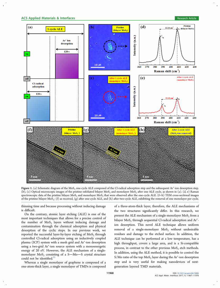
Figure 1. (a) Schematic diagram of the MoS2 one-cycle ALE composed of the Cl-radical adsorption step and the subsequent Ar+-ion desorption step.(b), (c) Optical microscopic images of the pristine exfoliated bilayer MoS2 and monolayer MoS2 after one ALE cycle, as shown in (a). (d, e) Ramanspectroscopic data of the pristine bilayer MoS2 and monolayer MoS2 that were observed after the one-cycle ALE. (f−h) TEM cross-sectional imagesof the pristine bilayer MoS2: (f) as received, (g) after one-cycle ALE, and (h) after two-cycle ALE, exhibiting the removal of one monolayer per cycle.
ACS Applied Materials & Interfaces Research Article
DOI: 10.1021/acsami.6b15886ACS Appl. Mater. Interfaces 2017, 9, 11967−11976
11968
■ RESULTS AND DISCUSSION
Figure 1a shows a schematic diagram of the cyclic etchingprocess that is composed of a sequential reactant-adsorptionstep and a reacted-compound-desorption step for the one-cycleMoS2 ALE. Figure 1b,c shows the optical microscopic images ofthe pristine bilayer MoS2 and the monolayer MoS2,respectively, after the one-cycle ALE of the bilayer MoS2.Figure 1d,e shows the Raman spectroscopic data of the pristinebilayer MoS2 and the monolayer MoS2, respectively, that wereobtained after the one-cycle ALE shown in Figure 1a. Throughthe adsorption of the reactive Cl radical on the bilayer MoS2surface for 120 s during the adsorption step and through thesubsequent Ar+-ion exposure with an adequate energy of ∼20eV (Figure S1a of the Supporting Information) for 120 s duringthe desorption step, a monolayer MoS2 could be obtained (i.e.,the monolayer MoS2 could be removed) from the bilayer MoS2by the one-cycle ALE;21 however, when the bilayer MoS2 wasprocessed with the Cl-radical-adsorption step for only 10 minor with the Ar+-ion desorption step for only 10 min, a change ofthe Raman spectroscopic data was not observed, indicating thatthe etching of the bilayer MoS2 did not occur with only Cl-radical adsorption or with only Ar+-ion bombardment (FigureS1b). Therefore, using ALE, the thickness of the MoS2 layerscould be precisely controlled (Figure S1c−f). Also, the MoS2thickness was observed for the as-received bilayer MoS2 afterthe one-cycle ALE and after the two-cycle ALE using cross-sectional TEM. As shown in Figure 1f−h, the removal ofexactly one MoS2 monolayer per ALE cycle could beconfirmed. In this study, the ALE mechanism of the MoS2layers was further investigated.During MoS2 ALE, when the MoS2-layer surface is exposed
to the Cl radicals, the Cl radicals fully cover the MoS2 surfaceand are chemisorbed onto the MoS2 surface. Also, when the Ar
+
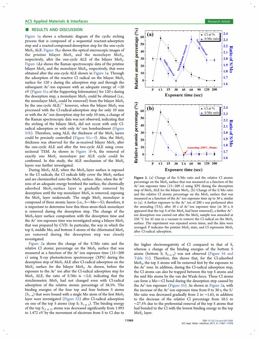
ions of an adequate energy bombard the surface, the chemicallyadsorbed MoS2-surface layer is gradually removed bydesorption until the top monolayer MoS2 is removed, exposingthe MoS2 layer underneath. The single MoS2 monolayer iscomposed of three atomic layers (i.e., SMoS); therefore, itis important to determine how this three-atom-thick monolayeris removed during the desorption step. The change of theMoS2-layer surface composition with the desorption time andthe Ar+-ion exposure time was investigated using a bilayer MoS2that was prepared by CVD. In particular, the way in which thetop S, middle Mo, and bottom S atoms of the chlorinated MoS2are removed during the desorption step was closelyinvestigated.Figure 2a shows the change of the S/Mo ratio and the
relative Cl atomic percentage on the MoS2 surface that wasmeasured as a function of the Ar+-ion exposure time (15−200s) using X-ray photoelectron spectroscopy (XPS) during thedesorption step of MoS2 ALE after Cl-radical adsorption on theMoS2 surface for the bilayer MoS2. As shown, before theexposure to the Ar+ ion after the Cl-radical adsorption step forMoS2 ALE, the ratio of S/Mo is ∼2.0, indicating that thestoichiometric MoS2 had not changed even with Cl-radicaladsorption of the relative atomic percentage of 58.5%. Thebinding energies of the four top and four bottom S atoms(S1−4) that were bound with a single Mo atom of the first MoS2layer were investigated (Figure S3) after Cl-radical adsorptionon one of the top S atoms (top S; S1 or 3). The binding energyof the top S(1 or 3) atoms was decreased significantly from 1.993to 1.472 eV by the movement of electrons from S to Cl due to
the higher electronegativity of Cl compared to that of S,whereas a change of the binding energies of the bottom Satoms (bottom S; S2 or 4) was not observed (Figure S4 andTable S1). Therefore, this shows that, for the Cl-adsorbedMoS2, the top S atoms will be removed first by the exposure tothe Ar+ ions. In addition, during the Cl-radical adsorption step,the Cl atoms can also be trapped between the top S atoms andthe mid Mo atoms by the van der Waals force. These Cl atomscan form a MoCl bond during the desorption step caused bythe Ar+-ion exposure (Figure S5). As shown in Figure 2a, withthe increase of the Ar+-ion exposure time from 0 to 30 s, the S/Mo ratio was decreased gradually from 2 to ∼1.65, in additionto the decrease of the relative Cl percentage from 58.5 to∼27.5% due to the preferential removal of the top S atoms thathad bonded to the Cl with the lowest binding energy in the topMoS2 layer.
Figure 2. (a) Change of the S/Mo ratio and the relative Cl atomicpercentage on the MoS2 surface that was measured as a function of theAr+-ion exposure time (15−200 s) using XPS during the desorptionstep of MoS2 ALE for the bilayer MoS2. (b) Change of the S/Mo ratioand the relative Cl atomic percentage on the MoS2 surface that wasmeasured as a function of the Ar+-ion exposure time up to 30 s, similarto (a). A further exposure to the Ar+ ion of 200 s was performed afterthe annealing (TA); after 30 s of Ar+-ion exposure time (at 30 s, itappeared that the top S of the MoS2 had been removed), a further Ar
+-ion desorption was carried out after the MoS2 sample was annealed at250 °C for 45 min in a vacuum to remove the Cl radical on the MoS2surface. The experiment was repeated seven times, and the data wereaveraged. P indicates the pristine MoS2 state, and Cl represents MoS2after Cl-radical adsorption.
ACS Applied Materials & Interfaces Research Article
DOI: 10.1021/acsami.6b15886ACS Appl. Mater. Interfaces 2017, 9, 11967−11976
11969
When the Ar+-ion exposure time was increased from 30 to 60s, the S/Mo ratio was increased from ∼1.65 to ∼2.31,indicating the removal of Mo below the top S atoms. Therelative Cl percentage continuously decreased from 27.5% at 30s to approximately 8.4% at 90 s, indicating the removal of Moby MoCl. The simulation results (Figure S6 and Table S2)show that when the Mo atoms are bonded with the trapped/adsorbed Cl atoms after the top S atoms were removed the Mo-binding energy decreased from 2.147 to 1.630 eV, whereas thebinding energy of the Mo atoms further increased from 2.147to 2.616 eV due to the tighter binding with the bottom S atomswhen the Mo atoms are not bonded to the trapped Cl atoms.The binding energy of the bottom S atoms did not changesignificantly after the top S atoms were removed, and itremained higher than that of the Mo atoms that were bondedwith Cl. Therefore, the increased S/Mo ratio for the Ar+-ionexposure time of 30−60 s should be related to the removal ofMoCl that formed on the first MoS2 layer during Cl-radicaladsorption.However, when the Ar+-ion exposure time was further
increased from 60 to 120 s, the S/Mo ratio was again decreasedfrom ∼2.31 to ∼2, indicating the removal of the bottom Satoms after the removal of the Mo atoms in the first MoS2layer. After the removal of the Mo in the first MoS2 layer, onlythe bottom S atoms remained. After the removal of the Moatoms, the binding energy of the bottom S atoms (bottomS(2 or 4) atoms can be bonded together, provided the van derWaals force is maintained between the bottom S atoms and thesecond MoS2 layer) decreases further from ∼1.91 to ∼1.51 eV(Figure S7 and Table S3) and the bottom S atoms arepreferentially removed by the Ar+ exposure from 60 to 120 s.The relative Cl percentage decreased from 8.4 to 0% during theAr+-ion exposure from 60 to 120 s. It is believed that the
remaining 8.4% of the Cl atoms at 90 s are related to thebonding of some of the Cl atoms (possibly by the dissociationof the removed MoCl) to the bottom S atoms. Theremaining Cl percentage also decreased to 0 after the Ar+-ionexposure of 120 s, indicating the exposure of the fresh secondMoS2 layer.After the preferential removal of the bottom S(2 or 4) atoms,
the second MoS2 layer was exposed. However, even though theAr+-ion exposure time was extended to 200 s after the firstMoS2 layer was completely removed at 120 s, the S/Mo ratioremained at ∼2, indicating that the second MoS2 layer was notetched by the Ar+-ion energy of 20 eV (Figure S1b). Thesimulation results are based on the A−A stacking of the bilayerMoS2, but the same results were obtained for the A−B stackingof the bilayer MoS2 (Figure S8 and Table S4).To investigate the importance of Cl-radical adsorption
between the top S atoms and the Mo atoms in MoS2 duringthe desorption step of MoS2 ALE, the remaining 27.5% of Clatoms on the first MoS2 layer after 30 s of the Ar
+-ion exposure,that is, after the removal of the top S atoms in the first MoS2layer, were removed by annealing in a vacuum (250 °C, 45min) and the annealed MoS2 sample was further exposed to theAr+ ions at 200 s. The S/Mo ratio and the relative Clpercentage that was measured by XPS are shown in Figure 2b.As shown in Figure 2b, after the annealing, the atomicpercentage of the Cl atoms of the MoS2 layer decreased to 0%due to the vaporization of the trapped/adsorbed Cl atoms fromthe first-MoS2-layer surface (the MoS2 layer after the top Satoms were removed). On the other hand, the S/Mo ratioremained the same as that before the annealing, indicating theremoval of only the Cl atoms on the surface by annealing. It isbelieved that the preferential removal of Cl on the first-MoS2-layer surface is related to the lower binding energy of Cl (0.881
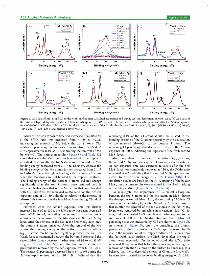
Figure 3. XPS data of Mo, S, and Cl on the MoS2 surface after Cl-radical adsorption and during Ar+-ion desorption of MoS2 ALE. (a) XPS data ofthe pristine bilayer MoS2 before and after Cl-radical adsorption. (b) XPS data of Cl before/after Cl-radical adsorption and after the Ar+-ion exposuretime of 0−200 s. XPS data of Mo and S after the Ar+-ion exposure of the Cl-adsorbed bilayer MoS2 for (c) 0, 15, 30 s, (d) 30, 45, 60 s, (e) 60, 90,120 s, and (f) 120, 200 s, and pristine bilayer MoS2.
ACS Applied Materials & Interfaces Research Article
DOI: 10.1021/acsami.6b15886ACS Appl. Mater. Interfaces 2017, 9, 11967−11976
11970
eV) when compared to that of Mo (1.630 eV) in the MoS2structure (Figure S6 and Table S2). After the removal of Cl onthe first-MoS2-layer surface, the Mo6+ peak at ∼236 eV wasobserved on the MoS2 surface in the XPS analysis, in additionto the redshifts of the Mo peaks (3d3/2 and 3d5/2) and the Speaks (2p1/2 and 2p3/2) (Figure S9). The Mo6+ peak is relatedto a defective MoS2 (i.e., MoSx, 1 ≤ × ≤ 2), and it is formed bythe binding of only the Mo atoms with the bottom S atomsafter the removal of the Cl atoms on the first MoS2 layer (thefirst MoS2 layer after the top S atoms are removed). Theremoval of Cl from the MoS2 surface also causes redshifts of theXPS peaks that are related to Mo and S. As mentioned earlier,after the top S atoms are removed, the binding energy betweenthe Mo and the bottom S atoms increased to 2.616 eV when noCl atoms are adsorbed on Mo. Therefore, as shown in Figure2b, for the annealed MoS2, the S/Mo ratio was not changedeven after the Ar+-ion exposure for 200 s due to the highbinding energy between the Mo and bottom S atoms. Thisindicates that no further etching of MoS2 occurred and revealsthe importance of Cl-radical adsorption on the Mo surfaceduring Mo ALE. In fact, the increase of the Mo6+ peak couldalso be related to the oxidation of the MoS2 surface after theannealing from the exposure to the air environment.22 In theexperiment in this study, the oxygen percentage that bonded tothe MoS2 surface could not be measured due to the use of SiO2as the substrate. If the Mo in MoS2 is bonded with oxygen, thebinding energy of the oxygen-adsorbed Mo in MoS2 (after thetop S atoms are removed) decreases from 2.616 to 1.986 eV(Figure S10 and Table S5); however, this is still much higherthan that (1.630 eV) of the Cl-adsorbed Mo in MoS2 (after thetop S atoms are removed). Therefore, removing the Mo atomsfrom MoS2 after the subsequent Ar+-ion exposure of 200 s isstill difficult. In Mo ALE, Cl-radical adsorption onto Mo isconsequently important for the preferential removal of Mofrom the MoS2 structure.Figure 3a shows the XPS data of Mo and S for the pristine
bilayer MoS2 and the Cl-adsorbed bilayer MoS2. After Cl-radical adsorption, the XPS peak intensities of Mo 3d and S 2pwere decreased because of the presence of 58.5% of Cl on theMoS2 surface. In addition, the XPS peak positions of Mo 3d3/2,Mo 3d5/2, S 2p1/2, and S 2p3/2 that are located at 232.4, 229.2,163, and 162 eV, respectively, were blue-shifted by approx-imately +0.3 to +0.4 eV because of the Fermi-level increasecaused by the movement of electrons from Mo and S to Cl witha higher electronegativity.23,24 Figure 3b shows the XPSnarrow-scan data for Cl in the pristine bilayer MoS2 and theCl-adsorbed bilayer MoS2 after the Ar
+-ion exposure from 0 to200 s. As shown, the Cl-peak intensity on the Cl-adsorbedbilayer MoS2 rapidly decreased from 0 to 30 s, followed by agradual decrease from 30 to 60 s and a slow decrease to zerofrom 60 to 120 s. After the Ar+-ion exposure time from 120 to200 s, the Cl-related peak was not observed.Figure 3c−f shows the XPS data of Mo and S for the MoS2
surface during the Ar+-ion desorption step of MoS2 ALE afterCl adsorption. As shown in Figure 3c,e, after the Ar+-ionexposure of the Cl-adsorbed bilayer MoS2, the XPS peakpositions were red-shifted back to the original pristine XPSpositions due to the removal of the Cl atoms on the bilayerMoS2 surface (Figure S11). Figure 3c shows the XPS narrow-scan data of Mo and S after the Ar+-ion exposure from 0 to 30s; these data are related to the removal period of the top Satoms of the first MoS2 layer. During the Ar
+-ion exposure from0 to 30 s, the peak intensities of Mo 3d3/2 and Mo 3d5/2 did not
change, whereas the peak intensities of the S 2p1/2 and S 2p3/2decreased due to the removal of the top S atoms on the firstMoS2 layer, in addition to the red-shifting of the peak positionsof Mo and S by approximately −0.2 to −0.3 eV, which is due tothe removal of some of the Cl atoms with the top S atoms.Figure 3d shows the XPS narrow-scan data of Mo and S after
Ar+-ion exposure from 30 to 60 s; these data are related to theMo atom removal period of the first MoS2 layer. As the Ar
+-ionexposure time was increased from 30 to 60 s, the peakintensities of Mo 3d3/2 and Mo 3d5/2 decreased due to theremoval of the Mo atoms in the first MoS2 layer, whereas thepeak intensities of S 2p1/2 and S 2p3/2 were increased due to theexposure of the bottom S atoms of the first MoS2 layer. Thepeak positions of Mo and S were further red-shifted byapproximately −0.1 eV due to the removal of Cl. Also, the peakintensity of SMoS at ∼226.8 eV, which is related to thecrystalline MoS2, was significantly decreased without anincrease of the peak intensity of Mo6+ at ∼236 eV, which isrelated to the defective MoS2. In general, when the MoS2 layeris physically damaged, the SMoS peak intensity at ∼226.8eV, which is related to the crystalline MoS2, was decreased, andthe Mo6+ peak intensity at ∼236 eV that is related to thedamaged MoS2 is increased.
21,22,25−27 It is believed that the lackof increase of the Mo6+ peak intensity while the SMoSpeak intensity decreased during MoS2 ALE is related to theremoval of Mo by MoCl, whereby the first MoS2 layer isundamaged even though only the (Cl)Mo bottom-S-atombonding remains in the first MoS2 layer.Figure 3e shows the XPS narrow-scan data of Mo and S after
the Ar+-ion exposure from 60 to 120 s that is related to theremoval period of the bottom S atoms of the first MoS2 layer.During the Ar+-ion exposure from 60 to 120 s, the peakintensities of Mo and S were gradually increased (in fact, therelative S intensity is decreased when it is normalized with theMo peaks, which is due to the removal of the remaining bottomS atoms of the first MoS2 layer) without changing the peakpositions of Mo and S. This indicates the gradual exposure ofthe second MoS2 layer as the top layer (as monolayer MoS2from bilayer MoS2) through the removal of the remainingbottom S atoms of the first MoS2 layer that bonded with thesecond MoS2 layer through the van der Waals force. Inaddition, along with the evidence of the exposure of the secondMoS2 layer, with the increase of the Ar
+-ion exposure time from60 to 120 s, the crystalline SMoS peak at ∼226.8 eV wasincreased without showing the defective Mo6+ peak at ∼236 eV.Also, the XPS peak-intensity ratios of Mo and S for the Cl-adsorbed bilayer MoS2 after the Ar
+-ion exposure of 120 s aresimilar to those of the pristine MoS2 layer (the peak ratios arethe same for both the MoS2 bilayer and the MoS2 monolayer).Changes of the peak positions of Mo and S are not noticeableduring the Ar+-ion exposure from 60 to 120 s, and this is relatedto the fact that a significant amount of adsorbed Cl did notremain on the MoS2 layer, with the possible exception of someof the bottom S atoms of the first MoS2 layer. In fact, after theAr+-ion exposure time of 60 s, the XPS positions of Mo and Shad shifted back to the locations that are similar to thepositions of pristine MoS2 due to the removal of most of the Clatoms that were adsorbed onto the MoS2 surface.The remaining MoS2 layer became a monolayer MoS2, and
the MoS2 layer was further exposed to the Ar+ ions from 120 to
200 s. As shown in Figure 3f, even after the Ar+-ion exposure of200 s, changes of the peak intensities and peak positions of Moand S were not observed, indicating that the MoS2 structure
ACS Applied Materials & Interfaces Research Article
DOI: 10.1021/acsami.6b15886ACS Appl. Mater. Interfaces 2017, 9, 11967−11976
11971
also remained unchanged. Also, because of the absence of anyMoS2 surface damage from the low-energy Ar+-ion exposure(approximately 20 eV), a change of the crystalline-SMoSpeak intensity and the existence of a defective Mo6+ peak were
not observed, even though the MoS2 layer was exposed by the200 s of Ar+ ions. Therefore, clean and undamaged monolayerMoS2 was exposed after the one-cycle of ALE of the bilayerMoS2.
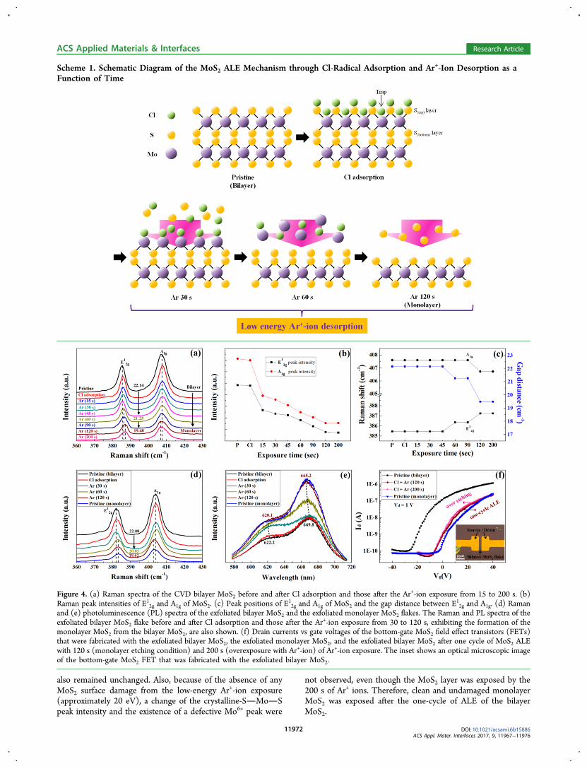
Scheme 1. Schematic Diagram of the MoS2 ALE Mechanism through Cl-Radical Adsorption and Ar+-Ion Desorption as aFunction of Time
Figure 4. (a) Raman spectra of the CVD bilayer MoS2 before and after Cl adsorption and those after the Ar+-ion exposure from 15 to 200 s. (b)Raman peak intensities of E1
2g and A1g of MoS2. (c) Peak positions of E12g and A1g of MoS2 and the gap distance between E1
2g and A1g. (d) Ramanand (e) photoluminescence (PL) spectra of the exfoliated bilayer MoS2 and the exfoliated monolayer MoS2 flakes. The Raman and PL spectra of theexfoliated bilayer MoS2 flake before and after Cl adsorption and those after the Ar+-ion exposure from 30 to 120 s, exhibiting the formation of themonolayer MoS2 from the bilayer MoS2, are also shown. (f) Drain currents vs gate voltages of the bottom-gate MoS2 field effect transistors (FETs)that were fabricated with the exfoliated bilayer MoS2, the exfoliated monolayer MoS2, and the exfoliated bilayer MoS2 after one cycle of MoS2 ALEwith 120 s (monolayer etching condition) and 200 s (overexposure with Ar+-ion) of Ar+-ion exposure. The inset shows an optical microscopic imageof the bottom-gate MoS2 FET that was fabricated with the exfoliated bilayer MoS2.
ACS Applied Materials & Interfaces Research Article
DOI: 10.1021/acsami.6b15886ACS Appl. Mater. Interfaces 2017, 9, 11967−11976
11972

Scheme 1 shows a schematic diagram of the detailed MoS2ALE mechanism for the one-cycle ALE from the bilayer MoS2to the monolayer MoS2 through Cl-radical adsorption and Ar+-ion desorption. When Cl atoms were adsorbed on the bilayerMoS2, these were adsorbed on the top S atoms of MoS2, wherethey are also trapped between the top S atoms and the Moatoms by the van der Waals force because six of the electrons inthe Mo atoms (4d55s1) are fully bound to the S atoms. After Cl-radical adsorption, the binding energy between S(top) and Mo(the binding between the S 3s23p4 and Mo 4d55s1) decreasedsignificantly (the binding energy of the top S atoms decreasedfrom 1.99 to 1.47 eV) due to the higher electronegativity of Clcompared to that of S. Therefore, during the Ar+-iondesorption, the top S atoms of the first MoS2 layer arepreferentially removed as SCl for the Ar+-ion desorptiontime from 0 to 30 s. After the removal of the top S atoms, thetrapped Cl atoms form MoCl bonding, the binding energybetween the Mo atoms and the bottom S atoms is significantlydecreased (the binding energy of the Mo atoms decreased from2.15 to 1.63 eV), and Mo is preferentially removed as MoClfor the Ar+-ion desorption time from 30 to 60 s. After theremoval of the top S and Mo atoms of the first MoS2 layer, onlythe bottom S atoms that bonded with the second MoS2 layerthrough the van der Waals force remain, and their bindingenergy decreased after the removal of the Mo atoms (thebinding energy of the bottom S atoms decreased from 1.91 to1.51 eV). Therefore, the bottom S atoms are finally removedduring the Ar+-ion desorption time from 60 to 120 s. After theAr+-ion exposure time of 120 s, the fresh second MoS2 layer(bilayer to monolayer) is exposed, and because of the low Ar+-ion desorption energy of 20 eV, the further exposure to the Ar+
ions does not change the exposed MoS2 monolayer structureafter the one-cycle MoS2 ALE.Figure 4a shows the Raman spectra of the CVD bilayer MoS2
before and after Cl adsorption and after the Ar+-ion exposurefrom 15 to 200 s. The MoS2 Raman spectra showed two peaksof E1
2g and A1g. It has previously been reported that not onlytheir peak intensities decrease but also the gap differencesbetween E1
2g and A1g decrease from ∼22 to ∼19 cm−1 as thelayer thickness was varied from the bilayer to mono-layer.8,16−21,25 As shown in Figure 4b, changes of the peakintensities of E1
2g and A1g were not observed after Cl-radicaladsorption; however, after the Ar+-ion exposure, a decrease ofthe Raman peak intensities was observed up to 120 s of the Ar+-ion exposure and no further change of the peak intensities wasobserved after 120 s of the Ar+-ion exposure, indicating thedecrease of the MoS2 layer from the bilayer to the monolayerafter 120 s of the Ar+-ion exposure. Measurement of the gapdistances between E1
2g and A1g showed a decrease in the gapsafter the Ar+-ion exposure, and the detailed changes of the peakpositions of E1
2g and A1g are shown in Figure 4c. As shown, asthe Ar+-ion exposure time was increased from 15 to 120 s, thegap distance decreased from ∼22.14 to ∼19.48 cm−1, indicatingthe change from a bilayer MoS2 to monolayer MoS2. Duringthe change from the bilayer MoS2 to the monolayer MoS2 from60 to 90 s, the gap distance showed a midvalue of ∼21.25 cm−1,which is possibly due to the changes of the interactionsbetween the atoms from the S(top)MoS(bottom) bonds to theMoS(bottom) bonds in the first MoS2 layer during MoS2ALE.28
To investigate the degree of damage on the monolayer MoS2that occurred after the etching of the bilayer MoS2 by the one-cycle MoS2 ALE, bottom-gate MoS2 FETs were fabricated with
the exfoliated pristine bilayer MoS2, the exfoliated pristinemonolayer MoS2, and the exfoliated monolayer MoS2 that wereobtained using the one-cycle ALE of the exfoliated bilayerMoS2. In MoS2-FET fabrication, the exfoliated MoS2 was usedinstead of the CVD MoS2 because the exfoliated MoS2 layerscomprise a stoichiometric and defectless MoS2. With theexfoliated MoS2 flakes, the bilayer and monolayer MoS2 wereselected by Raman spectroscopy, as shown in Figure 4d. One ofthe bilayer MoS2 flakes was etched using the one-cycle MoS2ALE with different Ar+-ion exposure times from 30 (partiallayer etch condition) to 120 s (monolayer etch condition),followed by the measurement of its Raman peak. The result isshown in Figure 4d. As shown in Figure 4d, the exfoliatedpristine bilayer MoS2 and the exfoliated pristine monolayerMoS2 show typical gap distances between E1
2g and A1g of∼22.08 and ∼19.62 cm−1, respectively. The monolayer MoS2that was obtained by the one-cycle ALE of the bilayer MoS2flake is ∼19.62 cm−1, indicating the formation of the monolayerMoS2. In addition, the intensities and gap distances of the E1
2gand A1g peaks in the Raman spectra gradually decreased withAr+-ion exposure from 30 to 120 s. These results are verysimilar to those of the CVD MoS2 shown in Figure 4a.Figure 4e shows the PL spectra of the exfoliated bilayer
MoS2, exfoliated monolayer MoS2, exfoliated bilayer MoS2before and after Cl adsorption, and those after the Ar+-ionexposure from 30 to 120 s. Two peaks were observed in the PLspectra. The peak at ∼665 nm was due to the direct bandstructure at the K point of the Brillouin zone, and the peak at∼620 nm was due to the splitting of the valence band fromspin−orbit coupling.29,30 The PL spectra were normalized bythe Raman A1g peak intensity to avoid distortions caused byexternal environmental factors.13,31 The PL intensity wasalmost unchanged after Cl adsorption on the bilayer MoS2,but the PL intensity gradually increased with Ar+-ion exposurefrom 30 to 120 s. Also, the PL peak position was gradually blue-shifted from 669.8 to 665.2 nm. These results are due to theband gap transitions from the indirect to the direct band gapaccording to the sequential removal of S(top), Mo(mid), andS(bottom). In addition, the PL spectra of the exfoliated monolayerMoS2 and the exfoliated bilayer MoS2 after the one-cycle ALEare very similar, indicating that the single monolayer has beenvery effectively removed.Using the exfoliated bilayer MoS2, exfoliated monolayer
MoS2, and exfoliated bilayer MoS2 after the one-cycle ALE withAr+-ion exposure for 120 s (monolayer etch condition) to 200 s(overexposure condition), bottom-gate MoS2 FETs werefabricated, and the characteristics of the drain currents versusthe gate voltages (Id vs Vg) of the MoS2 FETs are shown inFigure 4f. The inset shows an optical microscopic image of oneof the ∼3 μm channel bottom-gate MoS2 FETs that werefabricated, for which 300 nm thick SiO2 was used as the gatedielectric and 80 nm thick Au was used for the source and drainelectrodes. As shown in Figure 4f, the MoS2 FETs that werefabricated with the pristine bilayer MoS2 and pristinemonolayer MoS2 exhibited the typical electrical characteristicsof the MoS2 FETs. Also, the MoS2 FETs that were fabricatedwith MoS2 and obtained after the one-cycle ALE of the bilayerMoS2 with Ar+-ion exposure of 120 and 200 s exhibited similarelectrical characteristics as those of the FETs fabricated with apristine monolayer MoS2. The field-effect mobility (μ) of thefabricated MoS2 FETs was calculated using the followingequation: μ = (dId/dVg) × [L/(WCiVd)], where L is thechannel length and W is the channel width (L and W were
ACS Applied Materials & Interfaces Research Article
DOI: 10.1021/acsami.6b15886ACS Appl. Mater. Interfaces 2017, 9, 11967−11976
11973
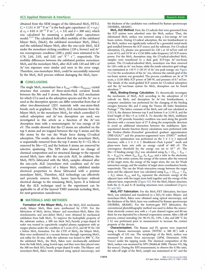
obtained from the SEM images of the fabricated MoS2 FETs).Ci = 1.151 × 10⁻⁴ F m−2 is the back-gate capacitance (C = ε0εr/d; ε0 = 8.85 × 10⁻¹² F m−1, εr = 3.9, and d = 300 nm), whichwas calculated by assuming a parallel plate capacitancemodel.32,33 The calculated field effect mobility of the exfoliatedbilayer MoS2 (black), the exfoliated monolayer MoS2 (blue),and the exfoliated bilayer MoS2 after the one-cycle MoS2 ALEunder the monolayer etching condition (120 s, brown) and Ar+
ion overexposure condition (200 s, pink) were estimated to be5.78, 2.65, 2.03, and 2.02 cm2 V−1 s−1, respectively. Themobility differences between the exfoliated pristine monolayerMoS2 and the monolayer MoS2 after ALE with 120 and 200 s ofAr+-ion exposure were similar and were in the error range.Therefore, one-monolayer MoS2 could be successfully removedby the MoS2 ALE process without damaging the MoS2 layer.
■ CONCLUSIONSThe single MoS2 monolayer has a S(top)MoS(bottom) crystalstructure that consists of three-atom-thick covalent bondsbetween the Mo and S atoms; therefore, the ALE mechanismfor which Cl is used as the adsorption species and the Ar+ ion isused as the desorption species can differ somewhat from that ofother two-dimensional (2D) materials with one-atom-thickbonds, such as graphene. The MoS2 ALE mechanism from thebilayer MoS2 to the monolayer MoS2, for which controlled Cl-radical adsorption and Ar+-ion desorption are used, wasinvestigated in this article as a function of the Ar+-iondesorption time with a monoenergetic Ar+-ion energy of 20eV. The results showed that the Cl atoms are adsorbed on thetop S atoms and are trapped between the top S atoms and theMo atoms by the van der Waals force during Cl-radicaladsorption. The results also showed that the monolayer MoS2is sequentially removed from the top S atoms by SCl, Mo isremoved by MoCl, and the bottom S atoms are removed byselective sputtering. The XPS data showed no change ofchemical composition and no structural damage to the exposedsecond MoS2 layer after the one-cycle ALE. In addition, theMoS2 FETs fabricated with the MoS2 samples obtained afterthe one-cycle ALE (monolayer etch condition and Ar+-ionoverexposure condition) of a bilayer MoS2 exhibited similarelectrical properties to those fabricated with a pristinemonolayer MoS2. Therefore, ALE technology can effectivelyand precisely remove MoS2 layers layer-by-layer withoutelectrical damage to the remaining MoS2 layers. It is believedthat the ALE technique used in the experiment can beapplicable to all of the layered TMD materials including MoS2for next-generation nanodevices.
■ MATERIALS AND METHODSFormation of the Bilayer MoS2. For the MoS2 ALE mechanism
study, bilayer MoS2 films were synthesized by CVD. For thefabrication of MoS2 device, bilayer- and monolayer-MoS2 flakes (forstoichiometric and zero-defect MoS2) were obtained by mechanicalexfoliation from bulk MoS2. To improve the hydrophilic property ofthe substrate surface, a 300 nm thick SiO2/heavily p-type-doped Siwafer was treated in capacitively coupled plasma equipment with anoxygen plasma under the condition of 5 sccm of O2 and 60 W for 120s before MoS2 formation. For the CVD of MoS2, the bilayer MoS2films were synthesized in a vacuum furnace through vaporizing MoO3and sulfur for 20 min, while the substrate was heated to 800 °C. Forthe exfoliated MoS2, the MoS2 flakes were mechanically exfoliatedfrom the bulk MoS2 using Scotch tape, and they were then placed ontothe 300 nm thick SiO2/heavily p-type-doped Si wafer. The bilayer- andmonolayer-MoS2 flakes were obtained using optical microscopy, and
the thickness of the candidates was confirmed by Raman spectroscopy(HORIBA, ARAMS).
MoS2 ALE Method. First, the Cl radicals that were generated fromthe ICP system were adsorbed onto the MoS2 surface. Then, thechlorinated MoS2 surface was removed using a low-energy Ar+-ionbeam system. During Cl-radical adsorption, the ion bombardment tothe MoS2 surface was significantly reduced by a grounded metal-meshgrid installed between the ICP source and the substrate. For Cl-radicaladsorption, Cl2 plasma was generated for 120 s at 10 mTorr with 63sccm of Cl2 and 18 W of a 13.56 MHz radio frequency (rf) ICP-sourcepower. For the MoS2 desorption step, the Cl-radical-adsorbed MoS2samples were transferred to a dual grid, ICP-type Ar+-ion-beamsystem. The Cl-radical-adsorbed MoS2 monolayer was then removedfor 120 s with an Ar+-ion beam, while the inside extraction-grid voltagewas maintained at +10 V (∼20 eV of Ar+-ion peak energy; see FigureS1a) for the acceleration of the Ar+ ion, whereas the outside grid of theion-beam system was grounded. The process conditions are Ar of 70sccm, a 13.56 MHz ICP power of 200 W, and pressure of 6.7 mTorr.The details of the mesh-gridded ICP system for Cl-radical adsorptionand the Ar+-ion-beam system for MoS2 desorption can be foundelsewhere.21
MoS2 Binding-Energy Calculation. To theoretically investigatethe mechanism of MoS2 ALE according to the adsorption of Clradicals on MoS2 and desorption by Ar+-ion bombardment, acomputer simulation was performed for the changing of the bindingenergies between Mo and S using the Vienna Ab Initio SimulationPackage.34 The lattice constant of the MoS2 unit cell was calculated as3.213 Å, the distance between top S and bottom S as 3.159 Å, and thebond length of MoS as 2.436 Å. To describe the MoS2 multilayersystem, a 2D periodic boundary condition was used along the growthdirection with a vacuum layer of 27 Å along the nonperiodic directionto avoid an additional interaction between the multilayers. Spin-unpolarized density function theory calculations were performed withthe Perdew−Burke−Ernzerhof generalized gradient approximation(PBE-GGA)35 and the projector-augmented wave (PAW)36 method.Geometry optimization was performed on the 3 × 3 × 1 supercellstructure, with a 3 × 3 × 1 Monkhorst−Pack k-point37 mesh andplane-wave basis sets with an energy cutoff of 400 eV. Theconvergence threshold for the energy was set to 10−4 eV. TheMoS binding energy (EB) was calculated using EB = (Etot − Esub −ES − EvdW)/n, where Etot, Esub, ES, EvdW, and n refer to the electronicenergy of the entire system, the energy of the system after the removalof the target atom, the energy of the target atom, the van der Waalsinteraction energy, and the number of target atom coordination bonds,respectively. The van der Waals interaction energy between the targetatom and the adjacent layer was calculated using Evdw = (ES+AL − EAL− ES), where ES+AL and EAL represent the electronic energy of theadjacent layer with the target atom held together and the energy of theadjacent layer, respectively (Figure S2). For the MoS2 bilayer structure,both the A−A and A−B stacking structures were considered (FiguresS3 and S8).
MoS2-FET Fabrication. For the MoS2-FET fabrication, few-layerMoS2 was exfoliated and transferred to a SiO2/Si wafer. Bilayer- andmonolayer-MoS2 flakes were obtained using optical microscopy, andthe thickness of the MoS2 layer was confirmed by Raman spectroscopy(HORIBA, ARAMS). For the bottom-gate FET fabrication, theconventional photolithography method was used to define the source/drain electrode contact area with a ∼3 μm channel region and 80 nmthick Au was deposited by a thermal evaporation system. After a lift-offprocess, contact annealing (Ar: 96.1%, H2: 3.9%, 1 slm, and 200 °C for1 h) was performed prior to measurement to increase the contactproperty of the devices.
Characterization. The Raman and PL spectra were inspectedusing a Raman microscopic system (WITEC α 300 M+) with awavelength of 532 nm. The morphology of the MoS2 surface wasmeasured by atomic force microscopy (AFM, Dimension 3100,Veeco) under the tapping mode. The chemical composition of theMoS2 surface was measured by XPS (MultiLab 2000, Thermo VG, MgKα source). During the XPS measurement, to observe the S/Mo ratio,the take-off angle of the MoS2 sample was maintained at 45° and the
ACS Applied Materials & Interfaces Research Article
DOI: 10.1021/acsami.6b15886ACS Appl. Mater. Interfaces 2017, 9, 11967−11976
11974
peak energies were calibrated using the C1 peak at 284.5 eV. Theelectrical characteristics of the MoS2 FET were measured underambient conditions using Keithley 4200-SCS. The change of thethickness of the MoS2 layer before and after the ALE cycles wasobserved using field-emission transmission electron microscopy (JEOLJEM-2100F).
■ ASSOCIATED CONTENT
*S Supporting InformationThe Supporting Information is available free of charge on theACS Publications website at DOI: 10.1021/acsami.6b15886.
Calculation of binding energy according to Cl-radicaladsorption and Ar+-ion desorption on the bilayer MoS2structure (A−A stacking and A−B stacking) andadditional experimental data (PDF)
■ AUTHOR INFORMATION
Corresponding Authors*E-mail: [email protected] (G.Y.Y.).*E-mail: [email protected] (D.W.K.).
ORCIDJin Yong Lee: 0000-0003-0360-5059Sung Joo Lee: 0000-0003-1284-3593Yeon Sik Jung: 0000-0002-7709-8347Geun Young Yeom: 0000-0001-7516-8404NotesThe authors declare no competing financial interest.
■ ACKNOWLEDGMENTS
This work was supported by the Nano-Material TechnologyDevelopment Program through the National ResearchFoundation of Korea (NRF), funded by the Ministry ofEducation, Science and Technology (2012M3A7B4035323 and2016M3A7B4910429).
■ REFERENCES(1) Baugher, B. W.; Churchill, H. O.; Yang, Y.; Jarillo-Herrero, P.Optoelectronic Devices Based on Electrically Tunable pn Diodes in aMonolayer Dichalcogenide. Nat. Nanotechnol. 2014, 9, 262−267.(2) Jariwala, D.; Sangwan, V. K.; Lauhon, L. J.; Marks, T. J.; Hersam,M. C. Emerging Device Applications for Semiconducting Two-dimensional Transition Metal Dichalcogenides. ACS Nano 2014, 8,1102−1120.(3) Wang, Q. H.; Kalantar-Zadeh, K.; Kis, A.; Coleman, J. N.; Strano,M. S. Electronics and Optoelectronics of Two-dimensional TransitionMetal Dichalcogenides. Nat. Nanotechnol. 2012, 7, 699−712.(4) Geim, A. K.; Grigorieva, I. V. Van der Waals Heterostructures.Nature 2013, 499, 419−425.(5) Lee, C.; Yan, H.; Brus, L. E.; Heinz, T. F.; Hone, J.; Ryu, S.Anomalous Lattice Vibrations of Single-and Few-layer MoS2. ACSNano 2010, 4, 2695−2700.(6) Li, B.; Yang, S.; Huo, N.; Li, Y.; Yang, J.; Li, R.; Fan, C.; Lu, F.Growth of Large Area Few-layer or Monolayer MoS2 fromControllable MoO3 Nanowire Nuclei. RSC Adv. 2014, 4, 26407−26412.(7) Yang, S.; Kang, J.; Yue, Q.; Yao, K. Vapor Phase Growth andImaging Stacking Order of Bilayer Molybdenum Disulfide. J. Phys.Chem. C 2014, 118, 9203−9208.(8) Huang, Y.; Wu, J.; Xu, X.; Ho, Y.; Ni, G.; Zou, Q.; Koon, G. K.W.; Zhao, W.; Neto, A. C.; Eda, G.; et al. An Innovative Way ofEtching MoS2: Characterization and Mechanistic Investigation. NanoRes. 2013, 6, 200−207.
(9) Mak, K. F.; Lee, C.; Hone, J.; Shan, J.; Heinz, T. F. AtomicallyThin MoS2: A New Direct-gap Semiconductor. Phys. Rev. Lett. 2010,105, No. 136805.(10) Frey, G.; Elani, S.; Homyonfer, M.; Feldman, Y.; Tenne, R.Optical-absorption Spectra of Inorganic Fullerenelike MS2 (MMo,W). Phys. Rev. B 1998, 57, No. 6666.(11) Kam, K.; Parkinson, B. Detailed Photocurrent Spectroscopy ofthe Semiconducting Group VIB Transition Metal Dichalcogenides. J.Phys. Chem. 1982, 86, 463−467.(12) Liu, K.; Zhang, W.; Lee, Y.; Lin, Y.; Chang, M.; Su, C.; Chang,C.; Li, H.; Shi, Y.; Zhang, H.; et al. Growth of Large-area and HighlyCrystalline MoS2 Thin Layers on Insulating Substrates. Nano Lett.2012, 12, 1538−1544.(13) Jeon, J.; Jang, S. K.; Jeon, S. M.; Yoo, G.; Jang, Y. H.; Park, J.;Lee, S. Layer-controlled CVD Growth of Large-area Two-dimensionalMoS2 Films. Nanoscale 2015, 7, 1688−1695.(14) Dumcenco, D.; Ovchinnikov, D.; Marinov, K.; Lazic, P.;Gibertini, M.; Marzari, N.; Sanchez, O. L.; Kung, Y.; Krasnozhon, D.;Chen, M.; et al. Large-area Epitaxial Monolayer MoS2. ACS Nano2015, 9, 4611−4620.(15) Kim, H.; Ahn, C.; Arabale, G.; Lee, C.; Kim, T. Synthesis ofMoS2 Atomic Layer using PECVD. ECS Trans. 2013, 58, 47−50.(16) Castellanos-Gomez, A.; Barkelid, M.; Goossens, A.; Calado, V.E.; van der Zant; van der Zant, H. S. J.; Steele, G. A. Laser-thinning ofMoS2: On Demand Generation of a Single-layer Semiconductor. NanoLett. 2012, 12, 3187−3192.(17) Xiao, S.; Xiao, P.; Zhang, X.; Yan, D.; Gu, X.; Qin, F.; Ni, Z.;Han, Z. J.; Ostrikov, K. K. Atomic-Layer Soft Plasma Etching of MoS2.Sci. Rep. 2016, 6, No. 19945.(18) Liu, Y.; Nan, H.; Wu, X.; Pan, W.; Wang, W.; Bai, J.; Zhao, W.;Sun, L.; Wang, X.; Ni, Z. Layer-by-layer Thinning of MoS2 by Plasma.ACS Nano 2013, 7, 4202−4209.(19) Lu, X.; Utama, M. I. B.; Zhang, J.; Zhao, Y.; Xiong, Q. Layer-by-layer Thinning of MoS2 by Thermal Annealing. Nanoscale 2013, 5,8904−8908.(20) Wu, J.; Li, H.; Yin, Z.; Li, H.; Liu, J.; Cao, X.; Zhang, Q.; Zhang,H. Layer Thinning and Etching of Mechanically Exfoliated MoS2Nanosheets by Thermal Annealing in Air. Small 2013, 9, 3314−3319.(21) Lin, T.; Kang, B.; Jeon, M.; Huffman, C.; Jeon, J.; Lee, S.; Han,W.; Lee, J.; Lee, S.; Yeom, G.; Kim, K. Controlled Layer-by-layerEtching of MoS2. ACS Appl. Mater. Interfaces 2015, 7, 15892−15897.(22) Yang, X.; Fu, W.; Liu, W.; Hong, J.; Cai, Y.; Jin, C.; Xu, M.;Wang, H.; Yang, D.; Chen, H. Engineering Crystalline Structures ofTwo-dimensional MoS2 Sheets for High-performance Organic SolarCells. J. Mater. Chem. A 2014, 2, 7727−7733.(23) Yang, L.; Majumdar, K.; Liu, H.; Du, Y.; Wu, H.; Hatzistergos,M.; Hung, P.; Tieckelmann, R.; Tsai, W.; Hobbs, C.; Ye, P. D.Chloride Molecular Doping Technique on 2D Materials: WS2 andMoS2. Nano Lett. 2014, 14, 6275−6280.(24) Yang, L.; Majumdar, K.; Du, Y.; Liu, H.; Wu, H.; Hatzistergos,M.; Hung, P.; Tieckelmann, R.; Tsai, W.; Hobbs, C. In High-performance MoS2 Field-effect Transistors Enabled by Chloride Doping:Record Low Contact Resistance (0.5 kΩ· μm) and Record High DrainCurrent (460 μA/μm); Symposium on VLSI Technology (VLSI-Technology): Digest of Technical Papers; IEEE, 2014; pp 1−2.(25) Jeon, M. H.; Ahn, C.; Kim, H.; Kim, K. N.; Lin, T. Z.; Qin, H.;Kim, Y.; Lee, S.; Kim, T.; Yeom, G. Y. Controlled MoS2 Layer Etchingusing CF4 Plasma. Nanotechnology 2015, 26, No. 355706.(26) Baker, M.; Gilmore, R.; Lenardi, C.; Gissler, W. XPSInvestigation of Preferential Sputtering of S from MoS2 andDetermination of MoSx Stoichiometry from Mo and S Peak Positions.Appl. Surf. Sci. 1999, 150, 255−262.(27) Ma, Q.; Odenthal, P. M.; Mann, J.; Le, D.; Wang, C. S.; Zhu, Y.;Chen, T.; Sun, D.; Yamaguchi, K.; Tran, T.; et al. Controlled ArgonBeam-induced Desulfurization of Monolayer Molybdenum Disulfide. J.Phys.: Condens. Matter 2013, 25, No. 252201.(28) Wieting, T.; Verble, J. Interlayer Bonding and the LatticeVibrations of β-GaSe. Phys. Rev. B 1972, 5, No. 1473.
ACS Applied Materials & Interfaces Research Article
DOI: 10.1021/acsami.6b15886ACS Appl. Mater. Interfaces 2017, 9, 11967−11976
11975
(29) Splendiani, A.; Sun, L.; Zhang, Y.; Li, T.; Kim, J.; Chim, C.;Galli, G.; Wang, F. Emerging Photoluminescence in Monolayer MoS2.Nano Lett. 2010, 10, 1271−1275.(30) Zhu, Z.; Cheng, Y.; Schwingenschlogl, U. Giant Spin-Orbit-Induced Spin Splitting in Two-Dimensional Transition-MetalDichalcogenide Semiconductors. Phys. Rev. B 2011, 84, No. 153402.(31) Mak, K. F.; Lee, C.; Hone, J.; Shan, J.; Heinz, T. F. AtomicallyThin MoS2: A New Direct-Gap Semiconductor. Phys. Rev. Lett. 2010,105, No. 136805.(32) Lopez-Sanchez, O.; Lembke, D.; Kayci, M.; Radenovic, A.; Kis,A. Ultrasensitive Photodetectors Based on Monolayer MoS2. Nat.Nanotechnol. 2013, 8, 497−501.(33) Fang, H.; Tosun, M.; Seol, G.; Chang, T. C.; Takei, K.; Guo, J.;Javey, A. Degenerate N-Doping of Few-Layer Transition MetalDichalcogenides by Potassium. Nano Lett. 2013, 13, 1991−1995.(34) Kresse, G.; Furthmuller, J. Efficiency of ab-initio Total EnergyCalculations for Metals and Semiconductors using a Plane-wave BasisSet. Comput. Mater. Sci. 1996, 6, 15−50.(35) Perdew, J. P.; Burke, K.; Ernzerhof, M. Generalized GradientApproximation Made Simple. Phys. Rev. Lett. 1996, 77, No. 3865.(36) Blochl, P. E. Projector Augmented-wave Method. Phys. Rev. B:Condens. Matter Mater. Phys. 1994, 50, No. 17953.(37) Monkhorst, H. J.; Pack, J. D. Special Points for Brillouin-zoneIntegrations. Phys. Rev. B: Condens. Matter Mater. Phys. 1976, 13,No. 5188.
ACS Applied Materials & Interfaces Research Article
DOI: 10.1021/acsami.6b15886ACS Appl. Mater. Interfaces 2017, 9, 11967−11976
11976


![DNA Nanodevices based on i motif structuresdnatec09/presentations/2009_05_15_dnatec09... · DNA Nanodevices based on i‐motif structures ... Hao Yan [hao.yan@asu.edu] Challenges](https://static.fdocuments.in/doc/165x107/5c7f16b709d3f2aa3f8c1a71/dna-nanodevices-based-on-i-motif-structures-dnatec09presentations20090515dnatec09.jpg)