Atomic Layer Deposition of Chalcogenide Thin Films · Atomic Layer Deposition of Chalcogenide Thin...
11
PUBLICATION REVIEW ON ULTRATECH ALD SYSTEMS Atomic Layer Deposition of Chalcogenide Thin Films 1 09.10.2015
-
Upload
truongminh -
Category
Documents
-
view
226 -
download
0
Transcript of Atomic Layer Deposition of Chalcogenide Thin Films · Atomic Layer Deposition of Chalcogenide Thin...

PUBLICATION REVIEWON ULTRATECH ALD SYSTEMS
Atomic Layer Depositionof Chalcogenide Thin Films
1
09.10.2015
Highlights
q BenefitsofALDfornano-manufacturingofchalcogenidesq Atomiclevelthicknesscontrolq Depositionon3DnanostructuresusingExpoModeq Controlofcompositioninmulticomponentsulfidesq Widerangeofsulfidesdepositedbycustomers:q Cu2S,Sb2S3,In2S3,SnS,ZnS,PbS,Cu2ZnSnS4 forPVsq MoS2 for2Dmaterialsq CNThasextensiveR&Dandmanufacturingexperiencewithsulfides,e.g.,
Zn(O,S)andhandlingofH2Sq Keyusers:ArgonneNationalLab,StanfordU.,U.ofHamburg,U.of
Michigan
2

Introductionq Greatinterestinsulfides for
photovoltaics,photonics, catalysisq RequiresH2Sq Chalcogenidephotovoltaics
§ Absorber§ bandgapsandenergylevelsmore
suitablethanoxides§ 31-34%efficiencyat1-1.6eV§ CZTSquaternarysynthesizedforfirst
time§ Cu2SstabilizedbythinALDoxides
§ Buffer/Emitter§ In2S3,ZnS,andCdS, andZn(O,S)
q EnergyStorage§ Cu2S/CNTcathodes@260mAhg-1
§ Li2S@800mAhg-1
q Photonics§ ZnSforTFELdisplays(firstALD
industrialapplication)
3
1.Dasgupta,N.P.,etal.,AccountsChem Res48,341–348(2015).
Single junction efficiency limits
ALD sulfide absorbers

CIGS- Photovoltaics
4
q Absorber /buffer/TCOcombination determinesspectralcapturerange
q Maxefficiencytodateat20%q Complexheterojunction, wherebufferand
absorber interfacedeterminebandbendingandultimateefficiency
q Buffermaterial,composition, opticalproperties,andfilmuniformity arecrucial
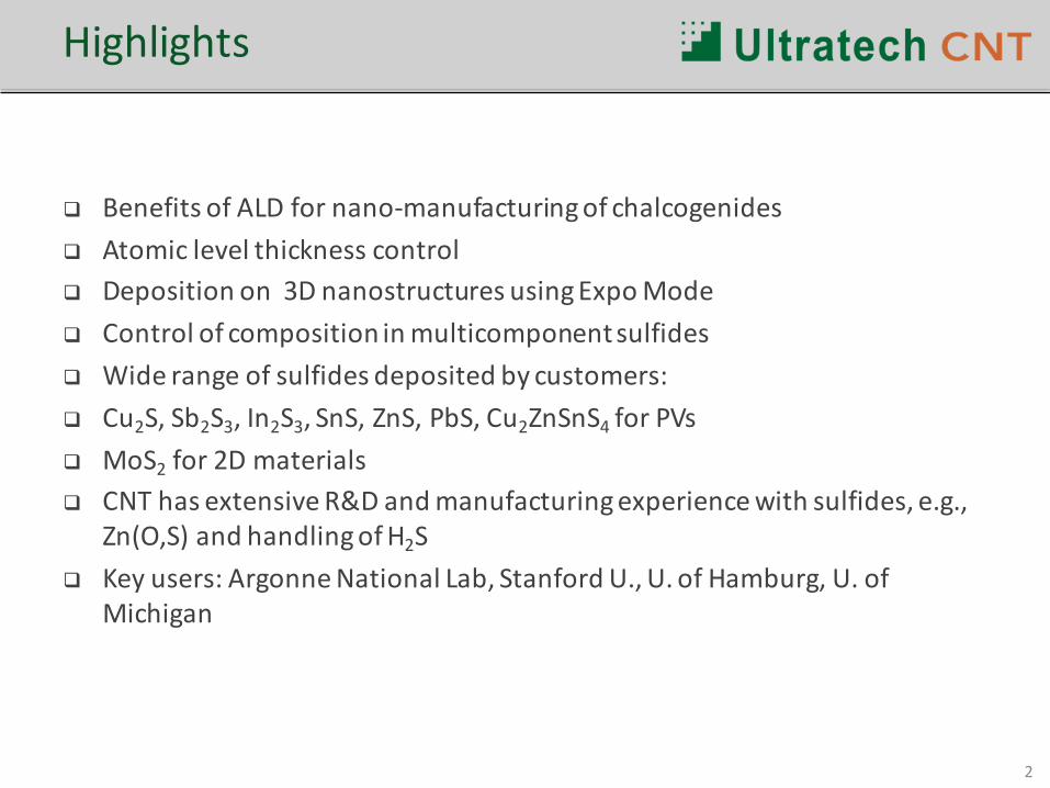
ZnO(1-x)Sx composition
5
Composition controlledbychanging thenumberofZnS/ZnOcyclesinorder tomatchgivenCIGScomposition
3.5
3.4
3.3
3.2
3.1
3.0
2.9
2.8
2.7
2.6
2.5
Ban
d Ga
p [e
V]
1.00.80.60.40.20.0
x - composition of ZnO(1-x)Snx
Quantumefficiencymeasurement
TEMcross-sectionofaCIGScellwithALDgrownZn(O,S)bufferlayer.
1.Bhargavaet.al.,JournaloftheKoreanPhysicalSociety,Vol53,No.5,,2008.2.ZimmermannU.,etal.,21stEur.PhotovoltaicSolarEnergyConference(2006),Dresden
x– compositionofZnO(1-x)Sx

Cu2ZnSnS4 (CZST)
6
q Objectives§ Lowcostseminconductor (CZST)for
photovoltaic§ 1.4eVbandgap,conformality in3D§ Compositional controlofquaternary
materialsq Experimental
§ SavannahS200,Expo,H2Skit,150˚C§ Cu2S:Cu2DBA(Strem)@160˚C+1%H2S§ SnS:TDMASn+1%H2S§ ZnS:DEZ+1%H2S§ 2strategies:trilayersandnanolaminates
Thimsenetal.,ChemistryofMaterials,24(16),3188–3196(2012).doi:10.1021/cm3015463
Cu2S/SnS2/ZnStrilayer depositedonasilicontrenchwafer

InterfaceandcompositionprofileinCZST
7
1.Thimsen,ChemistryofMaterials,24(16),3188–3196(2013)[Argonne]

Cu2SonSWCNT(100,200,400,600cycles)
Charge/dischargeforfirst3cyclesat1000mA/g
Cu2ScathodeforLIB
8
q Objectives§ Cu2Sdepositedonsinglewall
carbonnanotubesq Experimental
§ SavannahS200at135˚C,expomode
§ CuAMD(150˚C)and1%H2S§ SWCNTfunctionalized
with9minO3
q Results§ Core-shellSWCNT-n-Cu2Sexhibits
highchargedischarge/stability§ highcapacity(260mA/g)§ >99%Coulombicefficiency
1Meng,X.,JournalofPowerSources,2015,280,621–629 [ArgonneNL]

StabilizationofCu2SforPVs
9
q Cu2SPVabsorber§ abundant,nontoxic,
absorption>1E4cm-1
q IssuewithCu2S/CdSjunctionduetoCudiffusion
q S200forCu2SfromCuAMD/H2S@145˚C
q TiO2 ALDusedasCudiffusionbarrierandn-typeemittertoreplaceCdS
q 1-2Al2O3 cyclesreducecarrierconcentrationandstabilizefilmfor>2weeks
1.Riha,S.C.etalAcsApplMaterInter131010083550003 (2013).[ArgonneNL]
Carrierconcentrationfromin-situIV
PassivationofCu2SwithTiO2 &Al2O3/TiO2

In2S3 ALD
10
MassGainduringIn(amd)3 /H2Scycles
Absorptioncoefficientatvaryingdep.temperatures Impactofprocesstemperatureonn-typeIn2S3
q ChalcogenidePVtoreplaceCdS
q In(amd)3 andH2SinS200q Self-limitedALDupto225˚Cq 0.89Å/cycle@150˚Cq NodetectableC,N,O
halogen (RBS/AES)
1McCarthy,R.F.,etal,AcsApplMaterInter6,12137–12145(2014).[ArgonneNL]

Referencelist
11
1. Xu,J.etal. Atomiclayerdeposition ofabsorbing thinfilmsonnanostructuredelectrodesforshort-wavelengthinfraredphotosensing. Appl Phys Lett 107, 153105–5(2015).2. McCarthy,R.F.,Schaller, R.D.,Gosztola,D.J.,Wiederrecht,G.P.&Martinson,A.B.F.Photoexcited CarrierDynamicsofIn2S3ThinFilms. J.Phys.Chem.Lett. (2015).doi:10.1021/acs.jpclett.5b009353. Baryshev,S.V.,Riha,S.C.&Zinovev, A.V.SolarAbsorberCu2ZnSnS4 anditsParentMultilayersZnS/SnS2/Cu2SSynthesizedbyAtomicLayerDeposition andAnalyzedbyX-rayPhotoelectron Spectroscopy.Surf.Sci.Spectra 22, 81–99(2015).4. Riha,S.C.,Schaller,R.D.,Gosztola,D.J.,Wiederrecht,G.P.&Martinson,A.B.F.Photoexcited CarrierDynamicsofCu2SThinFilms.J.Phys.Chem.Lett. 5, 4055–4061(2014).5. Sutherland, B.R.etal. PerovskiteThinFilms viaAtomicLayerDeposition.AdvancedMaterials n/a–n/a(2014).doi:10.1002/adma.2014039656. McCarthy,R.F.,Weimer,M.S.,Emery,J.D.,Hock,A.S.&Martinson,A.B.F.Oxygen-FreeAtomicLayerDepositionofIndiumSulfide.Acs Appl MaterInter 6, 12137–12145(2014).7. Riha,S.C.etal. StabilizingCu2SforPhotovoltaicsOneAtomicLayerataTime.Acs Appl MaterInter131010083550003 (2013).doi:10.1021/am403225e8. Thimsen, E.etal. InterfacesandComposition ProfilesinMetal–SulfideNanolayers Synthesized byAtomicLayerDeposition.ChemMater 25, 313–319(2013).9. Thimsen, E.etal. AtomicLayerDeposition oftheQuaternaryChalcogenideCu2ZnSnS4.ChemMater 24, 3188–3196(2012).10. Yang,R.B.etal. PulsedVapor-Liquid-Solid GrowthofAntimony Selenide andAntimony SulfideNanowires.AdvancedMaterials 21, 3170–3174(2009).11. Dasgupta,N.P.,Walch,S.P.&Prinz,F.FabricationandCharacterizationofLeadSulfide ThinFilms byAtomicLayerDeposition.ECSTransactions 16, 29–36(2008).
SulfideworkdoneonUltratechCNTALDsystems


![Deposition and Characterisation of Chalcogenide … · Deposition and Characterisation of Chalcogenide Materials with the J/Lab FEL ... XRD Analysis of FEL Films ... [dB/km] traditional](https://static.fdocuments.in/doc/165x107/5b30c7e57f8b9a02638c1e34/deposition-and-characterisation-of-chalcogenide-deposition-and-characterisation.jpg)