Developing Atomic Layer Deposition Techniques of Tungsten ...

Atomic Layer Deposition for optical applications:
metal fluoride thin films
and novel devices
Tero Pilvi
Laboratory of Inorganic Chemistry Department of Chemistry
Faculty of Science University of Helsinki
Finland
Academic Dissertation
To be presented, with the permission of the Faculty of the Science of the
University of Helsinki for public criticism in Auditorium A110 of the Department of
Chemistry, A. I. Virtasen aukio 1, on the 5th of December 2008, at 12 noon.
Helsinki 2008
2
Supervisors Professor Mikko Ritala
and
Academy Professor Markku Leskelä
Laboratory of Inorganic Chemistry Department of Chemistry
University of Helsinki Helsinki, Finland
Reviewers Dr. Markku Ylilammi Thin Film Component VTT Micro and Nanoelectronics Espoo, Finland
Dr. Karol Fröhlich Institute of Electrical Engineering Slovak Academy of Sciences Bratislava, Slovak Republic
Opponent Dr. Jeffrey W. Elam Argonne National Laboratory
Energy Systems Division Argonne, Illinois, USA
© Tero Pilvi ISBN 978-952-92-4814-8 (paperback) ISBN 978-952-10-5133-3 (PDF version) http://ethesis.helsinki.fi Yliopistopaino Helsinki 2008

3
”The harder you work,
the luckier you get.”

4
ABSTRACT
Thin films of various metal fluorides are suited for optical coatings from infrared (IR) to ultraviolet (UV) range due to their excellent light transmission. In this work, novel metal fluoride processes have been developed for atomic layer deposition (ALD), which is a gas phase thin film deposition method based on alternate saturative surface reactions. Surface controlled self-limiting film growth results in conformal and uniform films. Other strengths of ALD are precise film thickness control, repeatability and dense and pinhole free films. All these make the ALD technique an ideal choice also for depositing metal fluoride thin films.
Metal fluoride ALD processes have been largely missing, which is mostly due to a lack of a good fluorine precursor. In this thesis, TiF4 precursor was used for the first time as the fluorine source in ALD for depositing CaF2, MgF2, LaF3 and YF3 thin films. TaF5 was studied as an alternative novel fluorine precursor only for MgF2 thin films. Metal-thd (thd = 2,2,6,6-tetramethyl-3,5-heptanedionato) compounds were applied as the metal precursors. The films were grown at 175–450 °C and they were characterized by various methods.
The metal fluoride films grown at higher temperatures had generally lower impurity contents with higher UV light transmittances, but increased roughness caused more scattering losses. The highest transmittances and low refractive indices below 1.4 (� = 580 nm) were obtained with MgF2 samples. MgF2 grown from TaF5 precursor showed even better UV light transmittance than MgF2 grown from TiF4. Thus, TaF5 can be considered as a high quality fluorine precursor for depositing metal fluoride thin films. Finally, MgF2 films were applied in fabrication of high reflecting mirrors together with Ta2O5 films for visible region and with LaF3 films for UV region.
Another part of the thesis consists of applying already existing ALD processes for novel optical devices. In addition to the high reflecting mirrors, a thin ALD Al2O3 film on top of a silver coating was proven to protect the silver mirror coating from tarnishing. Iridium grid filter prototype for rejecting IR light and Ir-coated micro channel plates for focusing x-rays were successfully fabricated. Finally, Ir-coated Fresnel zone plates were shown to provide the best spatial resolution up to date in scanning x-ray microscopy.

5
PREFACE
The research studies reported in this thesis was carried out during the years
2004–2008 in the Laboratory of Inorganic Chemistry in the University of
Helsinki.
First, I owe my deepest gratitude to my supervisors, professors Mikko Ritala
and Markku Leskelä for their invaluable contribution and help to this study.
Mikko, without your guidance this work would not have been done. Both of you
had always time for me and your rapid feedback concerning my papers was just
unbelievable. I had a great time during the years working in your laboratory.
Official reviewers Dr Markku Ylilammi and Dr Karol Fröhlich are warmly
acknowledged for the rapid and fluent review process and their valuable
suggestions to improve my thesis.
I am grateful to my co-authors for their expertise and fruitful collaboration. Many
thanks go to Joan Vila-Comamala, Konstantins Jefimovs and Christian David
for their valuable work in x-ray field in Switzerland. Warm thanks go to Martin
Bischoff, Norbert Kaiser and Ute Kaiser for their optical studies in Germany. I
am grateful also to Frans Munnik and Kai Arstila for their film composition
studies. Janne Laukkanen, Jari Turunen and Matti Kaipiainen are thanked for
their contribution in space projects. Esa Puukilainen is thanked for his AFM
measurements and Timo Hatanpää for synthesizing precursors. I am grateful
also to Suvi Haukka for her chemical reaction studies.
My special thanks go to my co-workers in our laboratory, Kaupo and Jaakko,
their support and advice during the years in and outside of the laboratory. I owe
warm thanks to Marianna for her kind advice and SEM/EDX measurements.
Warm thanks go to the rest of our ALD team: Elina, Emma, Tiina, room mate
Mikko, Marko, Jakke, Viljami, Jani, Timo, Jere, Kjell, Eero and Leo, and also to
all sähly players at Friday afternoon. Many thanks also to my ex-colleagues
Antti and Markus for their advices in laboratory and joyful moments outside of
work.

6
I am more than just thankful to my friends outside of academic world. Ibu,
Hessu and Edi without you guys (and the countless beers), this book would
have never been completed. Kissala team member Olli, your support “Anna
palaa” was valuable when I was finishing last part of the thesis. Pasi, Jukka,
Buge, Köpi, Happis&Maiju, Kajsa, Ira&Sami, Eero&Ale, Timo&Laura, and rest of
the friends and colleagues that are not mentioned here, thank you all for your
kind support.
Last, I owe my warmest gratefulness to my parents Ritva and Rami. Your
support and existence has been important during my studies. I want also thank
my brother Pasi for his friendship and joyful moments outside of science world. I
am thankful to my mother-in-law Marja for her support and that I was able to
write most part of this thesis at Marjan Maja in Estonia. Finally, most of all I am
grateful to my lovely wife Taru for her encouragement, endless support and
deep love.
Helsinki, November 2008
Tero Pilvi Tero Pilvi

7
LIST OF ORIGINAL PUBLICATIONS
This thesis is based on the following original publications (Studies I-VII)
I Pilvi, T., Arstila, K., Leskelä, M., Ritala, M.; Novel ALD process for
depositing CaF2 thin films; Chem. Mater., 19, (2007), 3387.
II Pilvi, T., Hatanpää, T., Puukilainen, E., Arstila, K., M., Bischoff, M.,
Kaiser, U., Kaiser, N., Leskelä, M., Ritala, M.; Study of novel ALD
process for depositing MgF2 thin films; J. Mater. Chem., 17, (2007),
5077.
III Pilvi, T., Puukilainen, E., Arstila, K., Leskelä, M., Ritala, M.; Atomic
layer deposition of LaF3 thin films using La(thd)3 and TiF4 as
precursors; Chem. Vap. Deposition, 14, (2008), 85.
IV Pilvi, T. Puukilainen, E., Munnik, F., Leskelä, M., Ritala, M.; ALD of
YF3 thin films from TiF4 and Y(thd)3 precursors, Chem. Vap.
Deposition, in Press.
V Pilvi, T., Puukilainen, E., Kreissig, U., Leskelä, M., Ritala, M.;
Atomic layer deposition of MgF2 thin films using TaF5 as a novel
fluorine source; Chem. Mater., 20, (2008), 5023.
VI K. Jefimovs, J. Vila-Comamala, T. Pilvi, J. Raabe, M. Ritala, and C.
David; Zone-doubling technique to produce ultrahigh-resolution x-
ray optics; Phys. Rev. Lett., 99, (2007), 264801.
VII Jefimovs, K., Laukkanen, J., Vallius, T., Pilvi, T., Ritala, M.,
Meilahti, T., Kaipiainen, M., Bavdaz, M., Leskelä, M., Turunen, J.;
Free-standing inductive grid filter for infrared radiation rejection;
Microel. Eng. 83, (2006), 1339.
The original publications are reprinted with the permission of the copyright
holders.

8
RELATED PUBLICATIONS BY THE SAME AUTHOR
1 Pilvi, T., Ritala, M, Leskelä, M., Bischoff, M., Kaiser, U., Kaiser, N.;
Atomic layer deposition process with TiF4 as precursor for
depositing metal fluoride thin films; Appl. Opt., 47, (2008), C271.
2 Laakkonen, P., Turunen, J., Pietarinen, J., Siitonen, S., Laukkanen,
J., Jefimovs, K., Orava, J., Ritala, M., Pilvi, T., Tuovinen, H.,
Ventola, K., Kaipiainen, M., Kuittinen, M.; Diffractive optics in
industry and research - novel components for optical security
systems; Proc. SPIE, 5954, (2005), 595402.

9
LIST OF ABBREVIATIONS AND ACRONYMS USED
� Absorption coefficient
acac 2,4-pentanedionato (acetylacetonato), [CH3C(O)CHC(O)CH3]–
ALD Atomic layer deposition
AFM Atomic force microscopy
Eg Band gap
CVD Chemical vapor deposition
EBE Electron beam evaporation
k Extinction coefficient
FESEM Field emission scanning electron microscopy
FZP Fresnel zone plate
GI-XRD Grazing incidence X-ray diffraction
IR Infrared
ITO Indium tin oxide
MCP Micro channel plate
PVD Physical vapor deposition
SEM Scanning electron microscopy
TEM Transmission electron microscopy
thd 2,2,6,6-tetramethyl-3,5-heptanedionato,
[(CH3)3CC(O)CHC(O)C(CH3)3]–
TMA Trimethylaluminum, Al(CH3)3
TOF-ERDA Time-of-flight elastic recoil detection analysis
UV Ultraviolet
VUV Vacuum ultraviolet
� Wavelength
XRD X-ray diffraction
XRR X-ray reflection

10

11
TABLE OF CONTENTS
ABSTRACT.............................................................................................................................4
PREFACE ...............................................................................................................................5
LIST OF ORIGINAL PUBLICATIONS.....................................................................................7
RELATED PUBLICATIONS BY THE SAME AUTHOR...........................................................8
LIST OF ABBREVIATIONS AND ACRONYMS USED ...........................................................9
1 INTRODUCTION ................................................................................................................13
2 BACKGROUND .................................................................................................................17
2.1 Light.............................................................................................................................17
2.2 Interaction of light with matter......................................................................................20
2.3 Interaction of light with film/substrate systems.............................................................26
2.4 Optical thin films ..........................................................................................................27
2.4.1 Interference coating design ..................................................................................28 2.4.2 Optical thin film materials .....................................................................................34 2.4.3 Common deposition techniques ...........................................................................39
2.5 Modern optics ..............................................................................................................40
2.6 ALD and optical thin films ............................................................................................43
3 EXPERIMENTAL................................................................................................................51
4 RESULTS AND DISCUSSION ...........................................................................................55
4.1 Novel ALD processes of metal fluorides ......................................................................55
4.1.1 Film growth...........................................................................................................55 4.1.2 Crystallinity and density........................................................................................58 4.1.3 Morphology and surface roughness .....................................................................61 4.1.4 Composition .........................................................................................................63 4.1.5 Optical properties .................................................................................................64 4.1.6 Electrical properties..............................................................................................66
4.2 High reflecting coating / bandpass filter .......................................................................68
4.3 Anti-tarnishing coating .................................................................................................74
4.4 Inductive grid filters......................................................................................................75
4.5 Micro channel plates....................................................................................................78
4.6 Fresnel zone plates .....................................................................................................82
5 SUMMARY AND CONCLUSIONS .....................................................................................89
6 REFERENCES ...................................................................................................................93

12

13
1 INTRODUCTION
Nowadays the push for higher density semiconductor devices, such as personal
computers and mobile phones, requires smaller circuit features.1 These can
only be obtained by reducing the wavelength in the photolithographic process
used to create the circuits, and by using better materials. Therefore optical
components and their coatings are being forced to operate at wavelengths even
in the deep ultraviolet (UV) region. As the excimer lasers extend to these
wavelengths the requirements for low optical loss components increases
radically.2 The usage of oxide materials is limited due to their intrinsic
absorption. However, fluoride compounds can be applied at these shorter
wavelengths.
Thin films of various metal fluorides are suited for optical coatings in infrared
(IR) and UV laser applications due to their excellent light transmission from the
UV to IR region.3 Mainly physical vapour deposition (PVD) methods, especially
evaporation techniques, have been applied for depositing these metal fluoride
films.3-6 However, the main limitation of evaporated fluoride films has been that
they are porous with low packing densities.7 Another problem in PVD methods
is how to control the exact thickness of layers in multilayer stacks.8
Chemical vapour deposition (CVD) of fluoride films has not been adapted widely
so far due to difficulties in handling the fluorine precursors, namely hazardous
HF and F2 gas.9 Atomic layer deposition (ALD) is a special variant of the CVD
technique invented in 1974 in Finland by Suntola and co-workers to produce
thin films for electroluminescent flat panel displays. In ALD,10,11 the film grows
via saturative surface reactions, typically producing pinhole free thin films with
good conformality and excellent thickness uniformity,12 making it a perfect
method-of-choice for also depositing metal fluoride thin films. The problem in
depositing fluoride films by ALD has been a lack of good fluorine source. HF,
obtained by thermally decomposing NH4F, was applied as the first fluorine
source in ALD for depositing CaF2, ZnF2, and SrF2 films.13 However, HF is not
an ideal choice for ALD because in addition to its unsafe chemical nature it
etches glass and many oxides. Hence, there is a clear need for a better

14
fluorinating agent.
The aim of this study was, first, to develop novel ALD processes with better
fluorine precursors for metal fluorides, and to study film growth as well as film
properties. The second aim was to study the applicability of the new ALD
processes in fabrication of a high reflecting multilayer stack for visible and UV
region. The third and last aim was to apply already existing ALD processes for
novel optical applications, especially for x-ray optics.
In this thesis, light and its interaction with matter and film/substrate systems are
described. Different optical thin film materials are presented from the ALD point
of view. Optical designs for one- and multilayer structures are introduced. The
experimental section describes the set-up in the film growth studies and
characterization methods used. Then the results on the new ALD processes of
metal fluorides are reviewed and discussed. Finally, some novel optical
applications of ALD are introduced with some basic background information
when relevant.

15

16

17
2 BACKGROUND
This chapter consists of background information needed for understanding of
optical thin films. As a starting point, the light itself and its spectral regions are
described.
2.1 Light
The light is electromagnetic radiation (or energy) and just one portion of the
various waves flying through space.14 The electromagnetic spectrum covers an
extremely broad range, from radio waves with wavelengths (�) of a meter or
more, down to x-rays with wavelengths less than a billionth of a meter. A
numerical equation relating the photon energy and the wavelength is15:
1240( )( )
( )hc eV nmnmE E eV
� �� � (1)
where h is the Planck’s constant, c is the velocity of light, and E is the energy of
a photon.
Optical radiation lies between radio waves and x-rays on the spectrum,
exhibiting a unique mix of ray, wave and quantum properties. At x-ray and
shorter wavelengths, electromagnetic radiation is particle like what comes to
ionisation and wavelike what comes to diffraction, whereas toward longer
wavelengths the behaviour is mostly wavelike. The visible portion occupies an
intermediate position, containing both particle and wave properties in varying
processes. The relationship between the wavelength and energy of radiation is
inverse, such that long wavelength radiation has lower energy than short
wavelength radiation (Eq. 1).
Wavelength ranges for spectral regions starting from infrared (IR) down to x-
rays are introduced in Table 1. IR light with wavelengths above 700 nm contains
the least amount of energy per photon of any other range. IR radiation is unique
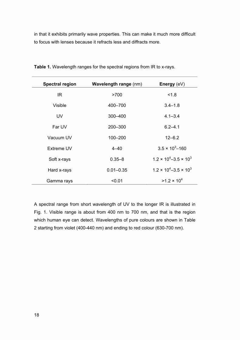
18
in that it exhibits primarily wave properties. This can make it much more difficult
to focus with lenses because it refracts less and diffracts more.
Table 1. Wavelength ranges for the spectral regions from IR to x-rays.
Spectral region Wavelength range (nm) Energy (eV)
IR >700 <1.8
Visible 400–700 3.4–1.8
UV 300–400 4.1–3.4
Far UV 200–300 6.2–4.1
Vacuum UV 100–200 12–6.2
Extreme UV 4–40 3.5 × 10³–160
Soft x-rays 0.35–8 1.2 × 10⁴–3.5 × 10³
Hard x-rays 0.01–0.35 1.2 × 10⁴–3.5 × 10³
Gamma rays <0.01 >1.2 × 10⁴
A spectral range from short wavelength of UV to the longer IR is illustrated in
Fig. 1. Visible range is about from 400 nm to 700 nm, and that is the region
which human eye can detect. Wavelengths of pure colours are shown in Table
2 starting from violet (400-440 nm) and ending to red colour (630-700 nm).
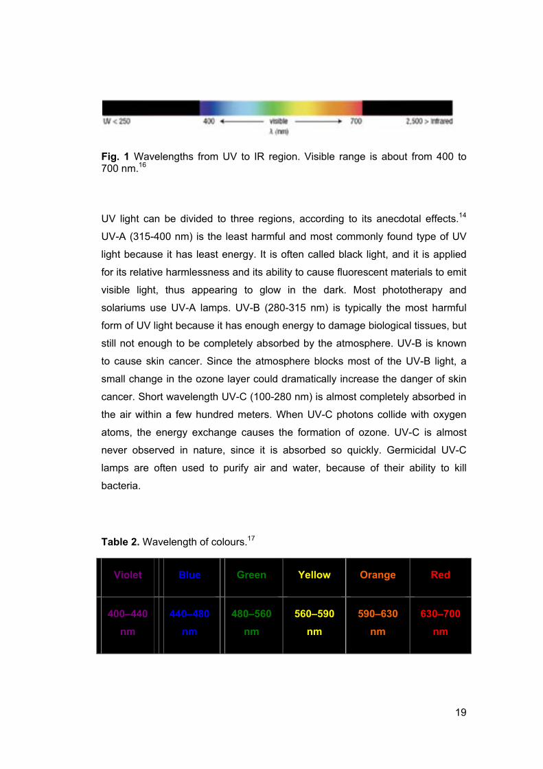
19
Fig. 1 Wavelengths from UV to IR region. Visible range is about from 400 to 700 nm.16
UV light can be divided to three regions, according to its anecdotal effects.14
UV-A (315-400 nm) is the least harmful and most commonly found type of UV
light because it has least energy. It is often called black light, and it is applied
for its relative harmlessness and its ability to cause fluorescent materials to emit
visible light, thus appearing to glow in the dark. Most phototherapy and
solariums use UV-A lamps. UV-B (280-315 nm) is typically the most harmful
form of UV light because it has enough energy to damage biological tissues, but
still not enough to be completely absorbed by the atmosphere. UV-B is known
to cause skin cancer. Since the atmosphere blocks most of the UV-B light, a
small change in the ozone layer could dramatically increase the danger of skin
cancer. Short wavelength UV-C (100-280 nm) is almost completely absorbed in
the air within a few hundred meters. When UV-C photons collide with oxygen
atoms, the energy exchange causes the formation of ozone. UV-C is almost
never observed in nature, since it is absorbed so quickly. Germicidal UV-C
lamps are often used to purify air and water, because of their ability to kill
bacteria.
Table 2. Wavelength of colours.17
Violet Blue Green Yellow Orange Red
400–440 nm
440–480 nm
480–560 nm
560–590 nm
590–630 nm
630–700 nm

20
The ability to use extreme UV (EUV) and soft x-rays (1–40 nm, Table 1) in a
constructive way with various optics used at longer wavelengths has been
limited by fundamental physics of matter-radiation interaction.18 EUV/soft x-rays
are strongly absorbed by all materials, resulting in very small near-normal
reflectivity from any single interface boundary. Anyhow, x-rays are widely used
in imaging. The advantages of x-ray imaging compared to imaging with visible
light or electrons are the high penetration depth and the low level of diffuse
scattering, which allow for the non-destructive inspection of thick, non-
transparent objects.
2.2 Interaction of light with matter
The two most important properties in optical materials are refractive index (n)
and extinction coefficient (k). They determine materials’ suitability for optical
applications, and are closely related to their dielectric properties.19 As discussed
above, the light exhibits unique mix of ray, wave and quantum properties.
Velocity of light is constant (c = 3 × 10⁸ m/s) in vacuum, but the speed of light
decelerates in matter by a factor n (Fig. 2), which is also called refractive index
(Eq. 2):
velocity of light in vacuum =velocity of light in matter
n (2)
Therefore for the vacuum as well as for air n = 1.0, and for most of the dielectric
materials n � 1. The more optically dense the material is, the more the speed of
light is decelerated, and the higher refractive index is obtained. Materials can be
transparent or absorbing in which the optical constant (or complex index of
refraction), N, is given by (Eq. 3):
N = in k� (3)
where n is the real part of the refractive index (or often simply as the refractive
index because N is real in the ideal dielectric material)20, and k is the extinction
coefficient, which indicates the amount of absorption loss when the
electromagnetic wave propagates through the material. Both n and k are

21
depending on the wavelength and the absorption is zero in vacuum. The real
part of the refractive index may be smaller than 1 for elements and metals. For
example, n is 0.27 and k is 4.18 for pure silver (�=620 nm).15 For a non-
absorbing matter, the index of refraction is (Eq. 4):
r r = n � � (4)
where �r is relative permittivity, and �r is relative magnetic permeability, and for
the most of dielectric materials �r is around 1 at optical frequencies. Since
electrons are responsible for electronic polarizability and they can respond at
optical frequencies, �r is not unity at optical frequencies.17
Fig. 2 Velocity of light in vacuum is constant c (left). However, velocity of light in matter (right), decelerates by a factor of n which is called refractive index.
The refractive index of a material at optical frequencies is mainly determined by
the polarizability of the valence electrons.21 In elements with increasing atomic
weight the electron population is enlarged, which results in the shielding of the
positive charge of the nucleus, so that the polarizability of the valence electrons
and consequently the refractive index are increased, e.g., for Si n = 3.4 and for
Ge n = 4.0. Refractive index of a compound is depending on many factors, such
as density and chemical bonding, and is discussed in more details later.
The extinction coefficient k is the imaginary part (Eq. 3) of the complex
refractive index N. It assumes the role of an index of attenuation. If this
attenuation is caused by true absorption alone, it will be termed absorption

22
coefficient �. The absorption constant is defined as follows (Eq. 5)19:
4 = k�� (5)
where � determines the wave intensity (I) transmitted through an absorbing
medium (thickness x) by the exponential law of absorption, also called
Lambert’s law of absorption (Eq. 6):
0x = I eI ��
(6)
where I0 is the intensity at x = 0. Real solids have typical absorption coefficient
of about � =10-3 cm-1 in their transparency region, and � = 106 cm-1 in the
region of fundamental absorption outside the transparency band.22
Fig. 3 Normal incident case: part of the incident light is transmitted and some part is reflected back.
When the incident light meets the matter, some part of the light transmits the
matter, and some part is reflected back (Fig. 3). A phase shift in reflection is
180° if n2 > n1.23 When light hits a transparent material, electrons in this material
start to oscillate. This oscillation takes, momentarily, energy from the photon,
and then gives it back. Polarization of atoms leads to a deceleration of the light
propagation velocity in transparent material. Energy of the photon, and thus the
wavelength of light, is the same before and after this interaction. If material
contains substances which absorb photons with certain energy, i.e., light with
certain wavelength of the spectrum, energy of the oscillating electrons is not
returned to photon and absorption occurs. Energy of a photon makes an
electron to make a transition from ground or already excited state to higher
energy state. Fluorescence occurs when the excited state relax back to the

23
ground state with emission of photons with lower energy and longer wavelength
than those of the absorbed photons.
Fig. 4 Schematic curve of transmission vs. wavelength of an optical material.21
Fig. 4 depicts schematically the curve of transmission versus wavelength of an
optical material. The desired region of high transmittance (region II) is situated
between the short wavelength absorption edge (region I) and the long
wavelength limit (region III). Region I depends on the electronic structure of the
material (band gap), whereas region III is determined by lattice vibrations or, in
the case of semiconductors, by free carrier absorption.21 The extent and quality
of region II depends strongly on the material; on its stoichiometry and purity.
In addition to the two most important properties of materials, n and k,
reflectance of material has to be added.19 Reflection of an electromagnetic
radiation from the interface between two matters depends on the refractive
indices of the matters and the angle of incidence.19 The optical properties of
conductive materials like metals and semiconductors (at the photon energy
range above the energy gap) differ from those of optically transparent matter.19
Free electron absorbs the incident electromagnetic wave in a thin surface layer
and then releases the absorbed energy in form of secondary waves reflected
from the surface. Thus, the light reflection comes very strong, e.g., highly
conducting iridium reflects 69.7% and sodium even 99.8% of incident wave (at

24
580 nm). At very high photon energies, quantum effects, such as the internal
photoeffects, start playing a greater role, and the optical properties of these
materials become similar to those of insulators (low reflectance, existence of
Brewster’s angle, etc.).19 The reflectance (R) can be defined as the ratio of the
reflected and incident irradiances, as illustrated in Fig. 3 (Eq. 7)20:
1 2
2 1
2Reflected powerReflectance = Incident power
n nn n� �� � �� �
(7)
where n1 and n2 are the refractive indices of matters 1 and 2. The last form in
Eq. 7 applies only at perpendicular incidence. At the same way the
transmittance (T) can be defined as the ratio of the transmitted and incident
irradiances (Eq. 8)20:
� �1 2
1 22
Transmitted power 4Transmittance = Incident power
n nn n
��
(8)
For example for glass n2 = 1.5 (air n1 = 1.0) Eq. 7 gives R = 4.0% and Eq. 8
gives T = 96.0%.
So we can also write that transmittance is (Eq. 9):
T = 1 – R (9)
Transmittance through both surfaces of glass in air would be 96.0% of 96.0%,
i.e. total transmittance is around 92%. The index range of optical glasses is
around 1.4–1.9 in the visible region and the transmittance through a single lens
of n = 1.9 would be only 82%.
So far one has assumed that there is no absorption, but things go slightly more
complicated when including absorption of materials in calculations. Anyhow, for
any two absorbing matters, the normal incidence reflectance is (Eq. 10)19:
� �� �
1 2 2
1 2 2
2 2
2 2R
n n kn n k� �
�� � (10)
The transmitted light has the same frequency but a different velocity than the

25
incident light, as discussed already. Thus, the wavelengths are matching at
interface (Eq. 11):
2 2 1 1� = �n n � � � � �11�
Therefore the wavelength changes under refraction, decreasing on going to a
material of larger refractive index and vice versa.
Fig. 5 Incident light is reflected and transmitted/refracted at dielectric interface.
When the light strikes a matter at an angle which is not parallel to the plane
normal, the angle of reflection equals the angle of incident, �i = �r. The
transmitted light is bent, or refracted (Fig. 5). This bending is described by
Snell’s law (Eq. 12)17:
2 1t i sin � = sin �n n (12)
What is called complete internal reflection can occur when the velocity in the
second material is larger than in the first material (n2 < n1). In that case, the
transmitted angle �t (Fig. 5) is larger than the incident angle �i. When �t is 90°,
the incident light is at critical angle �c (Eq. 13):
2
1
c� = nn if n1 > n2 (13)
For angles exceeding �c, the light penetrates into the second material layer only

26
for a very short distance and all the light is reflected.
2.3 Interaction of light with film/substrate systems
After taking into consideration the light, its spectral regions, and its interaction
with matter, one can take closer look at film/substrate systems.
When the light strikes a film, it can either be reflected (R), transmitted (T) or lost
by absorption (A) or by scattering (S),24 as illustrated in Fig. 6. At every interface
with two materials the light is reflected again, if there is a difference in the
refractive indices between these two materials.
Fig. 6 The basic principle of interaction of incident light with air/film, film/glass, and glass/air interfaces. Incident beam divides into reflected, scattered, absorbed, and transmitted beams.
Sometimes there is a misunderstanding that the density of the compound is the
only impressive factor in defining the refractive index, but the type of chemical
bonding also influences the refractive index. Compounds with predominant ionic
bonding show lower refractive indices than compounds with a high degree of
covalent bonding; for example for CaF2 (n~1.4), for CaO (n~1.7), and for CaS
(n~2.1) (see Table 4). The most covalently bound CaS has the highest
refractive index even if it has the lowest density (order of densities is: CaO >
CaF2 > CaS).

27
The essential feature of dielectric optical thin film materials is their very low
absorption (� < 103 cm-1) in the relevant region of the spectrum (Fig. 4). One
reason for the increased extinction in the films is often the true absorption due
to small deviations from stoichiometry and contamination. In multilayer
structures the spectral transmission range is determined by the absorptions of
the individual coated layers. Another reason for the increased extinction in the
films is scattering (S), which is an essential loss mechanism of optical
components that is mainly caused by the roughness of the optical surfaces and
by volume imperfections. Such imperfections include rough internal boundaries,
porous microstructure, pinholes, cracks, microdust, etc.21, 25 Contamination
becomes more important in the VUV where the extinction coefficients of water
and of most organic compounds are higher by orders of magnitude compared to
the visible spectral range.26
The optical losses (L) are made up from (Eq. 14):
L = A + S (14)
After this (Eq. 9) can be written as follows (Eq. 15):
T = 1 – R – L = 1 – R – A – S (15)
In these equations (14–15): A is absorption, S is scattering, R is reflectance,
and T is transmittance (see Fig. 6). L depends strongly on cleanliness,
deposition method, and deposition conditions of the films.21 The production of
high quality thin films with low loss requires glasslike or amorphous films,
without internal boundaries, and with smooth surfaces.
2.4 Optical thin films
Optical thin films are widely used in many applications to control how the light is
reflected, transmitted, or absorbed as a function of wavelength.24 Typical layers
might range in thickness from 20 nm in the UV to many times that in the IR
region. As discussed earlier, for many applications the most important optical
properties are the refractive index n, the extinction coefficient k, and the
reflectivity. Evaluating the mechanical, chemical, and optical performance of a

28
coating is a major task in itself. All coatings, single or multilayer, must posses a
specified degree of quality in all the three areas mentioned. Optical coatings are
not generally expected to be able to withstand severe abrasive wear, while
coatings on high-speed tools are.
2.4.1 Interference coating design
A high reflecting coating or a bandpass filter is a multilayer stack of alternating
high and low refractive index materials. Thin film filters operate by interference
of the light reflected from each interface layer as the light passes through the
sample. When these light waves overlap in phase with each other, the
magnitude of the wave increases, and the interference is called a constructive.
When the light waves are out of phase they cancel each other out, called as a
destructive interference.
When incident light (I) strikes a film, it can either be reflected (R), transmitted
(T) or lost by absorption (A) or scattering (S),24 as illustrated in Fig. 6. If one
considers a light beam incident on a homogenous parallel-sided film, the
amplitude and polarization state of the light transmitted and reflected can be
calculated and controlled in terms of the incident angle and the optical
constants of the three materials involved.
Antireflecting coatings
Fig. 6 depicts the light from the incident medium (air) of refractive index n0
passing through thin film material of index n1, finally entering a substrate
material (glass) of index n2. The refractive index of air is equal to 1.0, the
refractive index of vacuum. The light transmittance through normal glass was
around 92%. Complex optical systems may have many lenses conjugated
together and the losses may totally be 50% or more. IR optics use very high
refractive index materials such as Ge, which has a reflectance of 35% per
surface. In addition to power loss, these reflections can cause “ghost” images,
thus it is vital to use antireflecting (AR) coatings on the lenses.

29
AR coatings were first applied to military optical instrument to reduce glare from
the surfaces of the large number of lenses used, e.g., in a periscope or
binocular viewer,27 and they were a German military secret until the early stages
of World War II. These AR coatings were initially single layer of CaF2 and later
MgF2. The surface reflectance of 4% could be reduced to only 1% in the visible
region.
AR films have typically low refractive indices (n1), lower than the refractive index
of the substrate (n2), n1 < n2. AR coatings operate on the principle of destructive
interference of the light reflected from the front and back surfaces of the AR
films.24 In both cases the reflection takes place of the surface of a higher
refractive index material, thereby causing the same 180° phase shift upon
reflection. To ensure that the relative phase shift is 180° (phase condition), the
optical thickness of the film should be made one quarter wavelength so that the
total difference in phase between the two beams will correspond to half
wavelength, which is 180°.28 As the light waves are out of phase they cancel
each other out. A minimum in reflection thus occurs at wavelengths fulfilling the
equation (Eq. 16)23:
� �12 2nd m �� � m = 0, 1, 2, 3,… (16)
where n is refractive index of film, d is physical thickness of film, and � is
vacuum wavelength of the light. Eq. 16 can be used for calculating the minimum
reflectance of a single layer as in Fig. 6 but at normal incidence for the
wavelength of interest �0, it simplifies to (Eq. 17):29
1 0 2
1 0 2
22
2
R=
n n nn n n
�
�
�� � �
(17)
Eq. 17 is a useful formula for estimating how well a particular single layer
coating will behave. One can calculate, e.g., the film refractive index needed for
zero reflectance at the design wavelength as (Eq. 18):
30
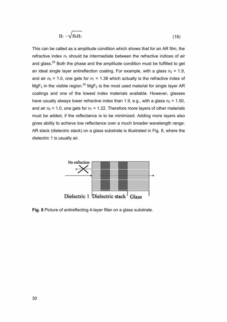
1 0 2 = n n n (18)
This can be called as a amplitude condition which shows that for an AR film, the
refractive index n1 should be intermediate between the refractive indices of air
and glass.28 Both the phase and the amplitude condition must be fulfilled to get
an ideal single layer antireflection coating. For example, with a glass n2 = 1.9,
and air n0 = 1.0, one gets for n1 = 1.38 which actually is the refractive index of
MgF2 in the visible region.30 MgF2 is the most used material for single layer AR
coatings and one of the lowest index materials available. However, glasses
have usually always lower refractive index than 1.9, e.g., with a glass n2 = 1.50,
and air n0 = 1.0, one gets for n1 = 1.22. Therefore more layers of other materials
must be added, if the reflectance is to be minimized. Adding more layers also
gives ability to achieve low reflectance over a much broader wavelength range.
AR stack (dielectric stack) on a glass substrate is illustrated in Fig. 8, where the
dielectric 1 is usually air.
Fig. 8 Picture of antireflecting 4-layer filter on a glass substrate.

31
Zero reflectance with two layers on substrate is achieved when (Eq. 19)28:
1
2 3
0
nn nn
� (19)
e.g., for a glass n3 = 1.52, air n0 = 1.00, and for MgF2 n1 = 1.38, one gets n2 =
1.70 which is a refractive index of MgO.20
Multilayer stacks
Optical surfaces are coated with functional multilayer designs for a variety of
purposes. The most common function is to reduce surface reflection. The
materials suitable for a specific coating design are chosen according to the
substrate material properties, the environment in which the coated surface will
be operated, optical performance, and sometimes cost of production.
The interference effect produces many interesting results. For example, in
interference filters the destructive effect is used to selectively filter light by
wavelength. A quarter-wave (QW) stack consists of alternate layers of high and
low n, each fulfilling equation (Eq. 20):
0
4j jnd �� � � � (20)
The multilayer is completely specified if we know nj, kj, and dj for each layer, n0
for the incident medium plus ns and ks for the substrate. Given the angle of
incident (�i), the reflectance (R) and the transmittance (T) can be calculated as
a function of wavelength. Modern techniques allow one to design optical
coatings with quite complicated spectral characteristics, and the main problem
nowadays is not to obtain a design with the required spectral properties but to
find the one which is most manufacturable.31 Commercially available software
program, namely Thinfilm, has been used in this work for analysis and
optimization of optical thin film design.32 More complicated designs are beyond
this thesis, but there are excellent references available.20, 28, 31
The QW multilayer stack has a characteristic high reflectance (HR) region or

32
stopband symmetric about the design wavelength �0 surrounded by long and
short wavelength pass regions characterized by many ripples in the passbands.
The width of the HR region is determined by the ratio of the high and low
refractive indices, nH/nL. The higher the ratio, the wider is the stopband. The
maximum reflectance depends on the number of the films as well as the ratio of
nH/nL with R increasing with the number of films (Fig. 9). The number of ripple
reflectance peaks depends also on the number of layers. QW stack is a good
starting design for edge filters and band pass filters of various type.31
Suppressing the ripple on one side of the HR region can create an edge filter,
e.g., a long wavelength pass (LWP) filter transmits the long wavelengths and
efficiently reflects the short ones. On the other hand a short wavelength pass
(SWP) filter transmits the short wavelengths and reflects the long ones. A
bandpass filter transmits a relatively narrow range of wavelengths and
effectively reflects those on both sides. Usually half wavelength cavity is used
and it is surrounded by QW stacks.
Fig. 9 Reflectance for normal incidence of alternating �0/4 layers of high refractive index (n = 2.3) and low (n = 1.38) dielectric materials on a glass substrate (n = 1.52) as a function of phase thickness or wavelength � for �0 = 460 nm. The number of layers is shown as a parameter on the curves.20
Once the design has been done, the wavelength characteristics can be moved
by changing the layer thicknesses by the same ratio, e.g., a LWP filter with an
edge at 400 nm can simply be shifted to 800 nm by making all the layers twice

33
as thick.
If the angle of incidence (�i, Fig. 6) increases, two effects are seen. First, the
effective thickness of the layers becomes smaller, which causes the filter to shift
to shorter wavelengths. Since the effect is inversely proportional to the film
refractive index, at large angles the films are no longer matched at the same
wavelength and the spectral shape degrades. The second effect at non-normal
incidence is that the spectral characteristics become dependent on the
polarization of the incident beam. This can be optimised and used to advantage
for such components as polarizing beamsplitters. But in general, these angle
effects are unfavourable.
For optimal performance of a multilayer the extinction coefficients of the
individual single films should not exceed 10-4. For example, in order to obtain
negligible losses in multilayer AR coatings, in a film 100 nm thick one can
tolerate only loss values of less than 0.01%, corresponding to a k value of 0.44
× 10-4 or an � value of 10 cm-1 at visible region.21
Nowadays reflection can routinely be reduced to 0.3% with help of multilayer
AR coatings that use materials of high and low refractive index pairs. One
application for AR coatings are silicon based solar cells, where the reflectance
loss of 36% can be reduced by a single AR coating to 12% or significantly better
by multilayer AR coatings to about 3%.33
The high and low refractive index material pairs in film stack can be applied in
colour selective coatings, in where the desired wavelength region reflects from
the surface. The colours created are caused by interference in multilayers that
are deposited onto glass, plastics, and non-transparent substrates, but simpler
renditions can be made by selectively anti-reflecting metals; in this design fewer
layers are required.34 HR mirrors can also be used in applications such as
decorative colour coatings in the commercial and entertainment world.

34
2.4.2 Optical thin film materials
One limitation in the optical thin film designing is the finite number of materials,
and therefore refractive indices, available.24 For multilayer stacks, the usual
goal is to have two materials with as different refractive indices as possible. This
gives the desired properties using the fewest number of layers in the stack. For
HR coatings there are plenty of materials available, but unfortunately that is not
the case in AR single layers; they are rare. In all cases, low absorption of the
film is desired.
Table 3. Commonly used optical thin film materials.24, 35
Material Refractive index (�=550–600 nm)
Transparency region (�m)
Si 4.1 1.1–14
CdS 2.5 0.5–>14
ZnS 2.35 0.38–25
TiO2 2.20–2.70 0.35–12
Ta2O5 2.16 0.30–10
ZrO2 2.10 0.34–12
HfO2 2.00 0.22–12
ITO 1.95–2.00 0.4–1.5
LaF3 1.60–1.61 0.2–12
Al2O3 1.59–1.63 0.20–7
ThF4 1.52 (at 400 nm) 0.20–15
SiO2 1.45 0.2–8
CaF2 1.43 0.15–12
MgF2 1.38 0.21–10
Table 3 shows some materials commonly used in optical thin film devices along
with their refractive indices. It should be noted that the refractive index depends

35
on the film deposition method. Compounds with predominant ionic bonding
show lower refractive indices than compounds with a high degree of covalent
bonding. CdS has a high refractive index of 2.5 and for ZnS n = 2.35. Sulphides
are applied as the high index component at the longer wavelengths, because
nearly all the commonly used metal oxide compounds absorb light at
wavelengths > 8 �m.34
Oxides. Oxides are an important class of optical coating materials because they
generally form hard, abrasion resistant, chemically and environmentally stable
films with a good variety of refractive indices and spectral ranges of high
transmission.35 Oxygen atoms form partially covalent bonds with metals that
account for the unique thermal stability of oxide compounds with quite high
refractive indices, but also for relatively narrow spectral ranges of
transparency.36 For example, TiO2 (n ~ 2.5) has a high refractive index in the
visible range (Table 3), but unfortunately it begins to absorb light below 450 nm,
rendering it useless for UV optics applications. The band gap and the variety of
possible crystal phases of TiO2 are properties responsible for its useful
reactivity in photocatalysis where incident light of energy greater than the 3 eV
band gap of TiO2 generates holes and electrons. These carriers produce the
oxidation and reduction reactions on the surface of TiO2 layers responsible for
the photocatalytic activity. These properties make TiO2 useful for applications
such as self-cleaning and defogging windows.
The coating materials used to make optical thin film filters for the visible region
are TiO2 and SiO2. But as TiO2 absorbs light also in the 900-1100 nm region
due to water absorption, Ta2O5 may be a better choice for wavelengths over
900 nm. Ta2O5 is a high refractive index material (n = 2.16) that has superior
optical behaviour to TiO2 in that it exhibits lower water absorptions in the near
IR. Therefore it is applied for wavelength division multiplexing filters and other
demanding applications.
ZrO2 and HfO2 and their silicates are very common thin film materials in
microelectronic applications due to their high permittivity values. ZrO2 is also a
useful optical material because of its great hardness, high UV transmission, and
high laser-induced damage threshold (LIDT) values.37 LIDT is the fluency at
which irreversible damage is created.38 Absorption of ZrO2 does not become

36
significant until close to 250 nm of wavelength. HfO2 can also be applied in
laser damage resistant coatings for the UV region.37 HfO2 and ZrO2 both can be
useful as UV coatings, but their refractive indices are just around 2.0 (Table 3),
so they require a greater number of high-low refractive index material pairs in
high reflection coating design in the visible region than, e.g., TiO2 or Ta2O5.
Indium tin oxide (ITO) is the most common example of a transparent conductive
oxide, while others are doped ZnO and SnO2. ITO, in where around 10% Sn is
generally added to In2O3, has a large band gap and is transparent between 400
nm and 800 nm. Refractive index of ITO is around 2.0. It begins to reflect light
at longer wavelengths so that at about 2.0 �m it behaves like metal and reflects
> 90%.27 The transition wavelength between transmission and reflection is
determined by the added carrier concentration in these films. The first
application for ITO was to defrost aircraft windows by sending a current through
the coating. ITO is also applied in transparent contacts, liquid crystal displays,
touch screens, solar cells, and anti-fogging windows. ITO is applied in thermal
control and architectural glass and windshields for its wavelength selective
(“green house”) properties to admit the visible wavelengths of the sun light but
prevent the heat escape.39 This can serve to reduce heating requirements
during cold weather, so the use of solar energy is maximized.
Generally the high refractive index oxide compounds begin to absorb at around
300 nm, e.g., TiO2 absorbs at as long wavelengths as 450 nm. Therefore, when
a thin film coating is needed for use below 350 nm, the number of candidate
oxides are quite limited, SiO2 and Al2O3 being the most common exceptions.40
SiO2 is one of the most desired optical materials together with MgF2 due to its
wide transmittance region of 0.2–8 �m.
Fluorides. Today research and development in UV coatings focuses on the
stringent requirements for optical components used in the new generations of
wafer-steppers for the semiconductor industry working at 193 nm (ArF-Excimer)
and 157 nm wavelength (F2-Excimer).35 The materials of choice for this
application are metal fluorides which exhibit sufficiently low absorption for the
vacuum UV region. As opposed to the oxides, fluoride compounds are
characterized by the formation of mostly ionic bonds due to the high
electronegativity of fluorine. Generally metal fluorides are dielectric materials

37
which are optically transparent over a wide range of wavelengths. Several
fluorides have a wide band gap around 10 eV and they are suitable for
applications in the wavelength range even below 200 nm.
LaF3 is a promising vacuum ultraviolet (VUV) transparent material. As LaF3 thin
films exhibit extremely good moisture resistance, they are very useful, e.g., for
protecting optical components.41 Even if LaF3 has a low n value of 1.6 (Table 3),
it is still the highest among VUV transparent films. Therefore LaF3 can be used
in multilayer stacks for constructing a high-low refractive index pair with, e.g.,
MgF2.42-51
CaF2 has a low refractive index of 1.4, and it belongs to those few materials that
have a lower refractive index than a bare glass. CaF2 is optically transparent
over a wide wavelength range from mid-IR to VUV,52 which makes bulk CaF2
useful for optical components such as UV laser systems, lenses, prisms and
windows.53, 54 In addition, CaF2 can be applied for optical multilayers and
filters.13, 55
MgF2 is the lowest refractive index material in Table 3 (n ~ 1.4). It is capable for
use in a wide wavelength region from 157 nm to around 10 �m.56 Therefore
improvements in its deposition are constantly under investigation. MgF2 has
been used as a low n material together with a high n material such as TiO2,57
Sc2O3,58 CeO2,8 Al2O3,59,60 and LaF342-51 in optical multilayers which can be
used, e.g., as the high reflectance mirrors for ArF excimer laser irradiation and
as narrow band pass filters.42 MgF2 thin films have also been applied in
multilayers with conducting materials, e.g. with Ag61-64 for flat panel displays and
electromagnetic shielding, and with ITO for solar cells.65 MgF2 is also widely
used for enhancing the reflectance of aluminum mirrors in the vacuum UV
region.7, 66-70 To avoid the aluminum oxidation, aluminum has to be covered with
a protective film. However, the cover layer can decrease the reflectance of Al,
especially in deep UV range, but MgF2 has good transmittance down there also.
The operational lifetimes of optical systems employing high power excimer
lasers are limited by the LIDTs of the coated components in the system.
Fluoride compounds satisfy laser damage requirements, and the candidate
materials can be: AlF3 and MgF2 for low refractive index material, and LaF3 and

38
GdF3 for high refractive index material.29
Semiconductors. Si and Ge are the most used semiconductors and can be
applied as high refractive index films in the IR region.35 Si is also used in
multilayer stacks in the EUV/x-ray region.
Metals. In EUV region nearly all materials usually absorb light strongly, making
it difficult to focus or otherwise manipulate light in this wavelength range.
Telescopes that form images with EUV light use multilayer mirrors that are
constructed of hundreds of alternating layers of high-mass metal, such as
molybdenum and tungsten, and a low-mass spacer such as silicon. Each layer
pair is designed to have a thickness equal to half wavelength of light to be
reflected. Metallic mirror is omnidirectional, which means it reflects light from
every angle, but it also absorbs a significant portion of the incident light,
whereas dielectric mirror does not contain free electrons and therefore can
reflect light more efficiently.
Al, Au, and Ag are highly reflecting metals (>90%), but they require abrasion
and chemical resistant dielectric overcoating because of their softness and
vulnerability to scratching. Hard metals like Rh, Ni, and Cr do not require
protection, but they reflect only <70%.35 Metal films are applied as reflectors,
semitransparent beam splitters, transparent conductive films, absorbers, and in
multilayer reflector stacks in the EUV/x-ray region. Al is widely used as a
reflector in the IR, visible and UV region. Protected silver films yield very high
reflecting mirrors for the visible and near IR region but still Al is most frequently
used in mirror coatings due to its superior long-term stability compared with
Ag.71 Semitransparent silver films can be used as transparent heat reflectors
and transparent conductive films.
Above percolation thickness, the optical behaviour of metal films is similar to the
corresponding bulk materials, and they are transparent to visible and reflective
for IR radiation as long as thickness is below about 20 nm.22 In this thickness
interval, transparent metal films can be applied as neutral beamsplitters, solar
control coatings, thermal insulating coatings, transparent electrodes, and
heating layers.22, 35

39
2.4.3 Common deposition techniques
Generally physical vapor deposition (PVD) methods and especially evaporation
have been the earlier work horse for fabricating optical coatings, but other
techniques are increasing their importance.
Every deposition technique has its own influence on film structure and on the
resulting properties. Therefore coating engineers are forced to make
compromises in adopting techniques that appear to be suitable for their current
specific coating needs.72 In the PVD methods the vaporized material is
transported through a reduced atmosphere and condensed on a non-heated or
heated and generally rotated substrate where the coating is formed.73
The production of coatings for the deep and vacuum UV (DUV/VUV) region is
still dominated by the thermal evaporation of a small class of fluoride materials
including LaF3 and MgF2 as the most prominent ones.25 However, these
materials tend to form coatings with a columnar microstructure containing
various defects and especially voids, which may absorb contaminants from the
environment.
If CaF2 is taken as an example thin film material, mainly PVD techniques have
been used for the film deposition, e.g., electron-beam evaporation (EBE),74-79
thermal evaporation,41,80-84 r.f. magnetron sputtering,85 pulsed laser
deposition,53 and molecular beam epitaxy (MBE),52,86-100 The sequence of
deposition processes yielding stable, harder and more adhesive coatings is said
to be as follows: resistance heated evaporation < e-beam evaporation <
sputtering < ion assisted deposition.34
Chemical vapor deposition (CVD) is a material synthesis method where the
constituents of a vapour phase participate heterogeneous reaction sequences
to form a solid film on a solid substrate.73 CVD of metal fluoride thin films has
not been adopted widely so far due to difficulties in handling the fluorine
precursors, namely hazardous HF or F2 gas.9 A few CVD processes have been
reported for depositing MgF2 films,9,101-103 LaF3 films,104,105 CaF2 films,106 and
YF3 thin films.107 Generally for interference optical thin film production, PVD
technologies are dominant, while CVD methods are rarely used.108
40
2.5 Modern optics
So far just classical thin film interference optics has been discussed, but new
modern optics is now briefly introduced with some practical examples.
Generally classical optics is understood as 2-D films, whereas the modern
optics as 3-D structures. The field of modern optics including diffractive and
reflective devices is growing fast at the moment and new applications based on
micro and nano optics are actively developed.
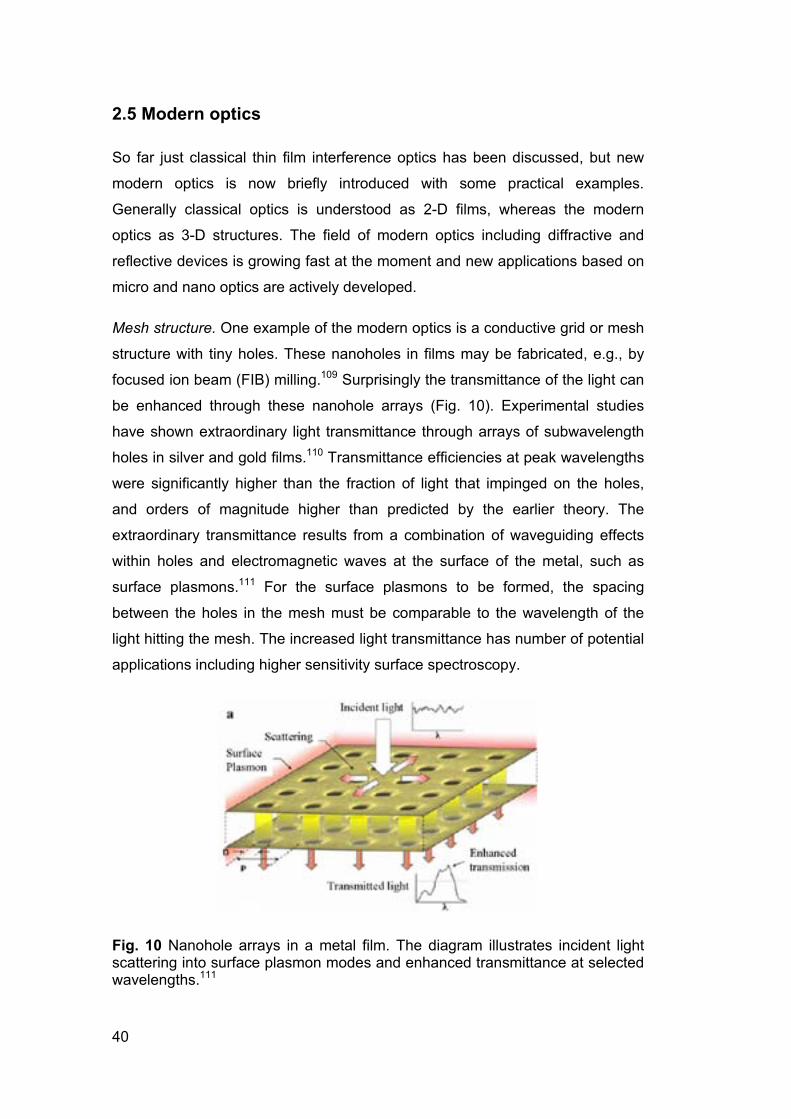
Mesh structure. One example of the modern optics is a conductive grid or mesh
structure with tiny holes. These nanoholes in films may be fabricated, e.g., by
focused ion beam (FIB) milling.109 Surprisingly the transmittance of the light can
be enhanced through these nanohole arrays (Fig. 10). Experimental studies
have shown extraordinary light transmittance through arrays of subwavelength
holes in silver and gold films.110 Transmittance efficiencies at peak wavelengths
were significantly higher than the fraction of light that impinged on the holes,
and orders of magnitude higher than predicted by the earlier theory. The
extraordinary transmittance results from a combination of waveguiding effects
within holes and electromagnetic waves at the surface of the metal, such as
surface plasmons.111 For the surface plasmons to be formed, the spacing
between the holes in the mesh must be comparable to the wavelength of the
light hitting the mesh. The increased light transmittance has number of potential
applications including higher sensitivity surface spectroscopy.
Fig. 10 Nanohole arrays in a metal film. The diagram illustrates incident light scattering into surface plasmon modes and enhanced transmittance at selected wavelengths.111
41
In addition to the enhanced light transmittance, the grid structure can also be
used for rejecting some part of the spectral range. For example, a inductive grid
filter for rejecting IR radiation while passing part of the visible light as well as x-
rays through has been fabricated,VII and will be discussed in more details in
Chapter 4.4.
When a matrix of hollow glass tubes is fused together, and drawn longer and
narrower, the result is a micro channel plate (MCP). MCPs are used for
focusing x-rays, and if the walls of the holes are coated with a thin metal layer
with high density, MCP can focus the x-rays much more efficiently, but
producing a smooth and conformal coating inside the micropores is a difficult
task and will be discussed more in Chapter 4.5.
Metamaterials. More recently, metamaterials has been a hot topic.109,112 The
metamaterials are artificially designed subwavelength composites possessing
extraordinary optical properties that do not exist in nature. Natural materials all
have a positive refractive index, but the metamaterials with negative refractive
indices refracts light opposite way to the natural materials. The metamaterials
can alter the propagation of electromagnetic waves, resulting in negative
refraction, subwavelength imaging, and cloaking. Negative refraction was
reported in bulk metamaterials composed of silver nanowires with a separation
distance much smaller than wavelength at optical frequencies (Fig. 11).112 A
porous alumina template was prepared by electrochemical anodization, into
which silver nanowires were electrochemically deposited.

42
Fig. 11 Negative refraction in bulk metamaterial was achieved at visible frequencies. (Left) Schematic of negative refraction from air into silver nanowires metamaterials. (Right) Nanowires embedded in an alumina matrix, as well as SEM images showing the top and side view of the nanowires (60 nm wire diameter and 110 nm centre to centre distance). The scale bars indicate 500 nm.112
Another recent example of metamaterials is so called fishnet structure that was
fabricated by evaporation and FIB (Fig. 12).109 The stack consists of alternating
layers of 30 nm Ag and 50 nm MgF2, and the dimensions of the structure
correspond to the diagram in Fig. 12a. The structure was fabricated so that the
3-D fishnet metamaterial can achieve a negative refractive index near the
visible region (�=1450–2200 nm)
Fig. 12 Diagram of the 21-layer fishnet structure (a) with a unit cell of p=860 nm, a=565 nm and b=265 nm. Cross-sectional SEM image of the fabricated fishnet structure is also shown (b).109

43
2.6 ALD and optical thin films
Due to the certain difficulties in PVD and CVD methods (Chapter 2.4.3), atomic
layer deposition (ALD) technique is considered as an option for depositing
optical thin films in this section. In addition to the ALD method itself, optical film
materials are introduced with some practical applications.
Because the evaporation distribution is not geometrically (and perhaps
compositionally) uniform, the properties of the coating can vary spatially over
the substrate holder.113 Applications such as thick metal mirror production are
not affected, but a uniform layer can be critical in the production of demanding
broadband and multiple-band antireflection coatings, narrow bandpass filters,
polarizing coatings, and hot/cold mirrors. On the other hand, conformal films are
needed for modern 3-D optics devices.
In ALD, the film growth takes place in a cyclic manner.12 In the simplest case,
one cycle consist of four steps: (1) exposure of the first precursor, (2) purge or
evacuation of the reaction chamber, (3) exposure of the second precursor, and
(4) purge or evacuation. This cycle is repeated as many times as necessary to
obtain the desired film thickness. As the film growth proceeds in a self-limiting
manner, each cycle deposits exactly the same amount of material. The ALD
process is schematically shown in Fig. 13 (left). Many ALD processes may be
performed over a relatively wide temperature range,12,114 and several low
temperature ALD processes were published recently.115
Controlling the film thickness in ALD is easy, because the film grows via
alternate saturative surface reactions. Surface controlled self-limiting film growth
results in conformal and uniform films (Fig. 13 right). Other strengths of ALD are
repeatability and dense and pinholes free films. The main drawback in ALD is
its slowness, but batch ALD offers higher throughput and potentially lower cost
than using single wafer cluster tools.116 Other challenges for ALD and especially
for optical thin films are: high deposition rate ALD processes, fabricating
artificial optical materials, and depositing highest and lowest refractive index
materials.117

44
Fig. 13 Principle of ALD film deposition cycle schematically illustrated by an example of the growth of TiO2 from TiCl4 and H2O precursors (left). Ion milled cross section of the opal photonic crystal (PC) with three-layer structure (right). The PC was fabricated by infiltration of opal template consisting of 466 nm silica spheres with 10 nm ZnS:Mn (layer 2) and 26 nm TiO2 (layer 1), removing the silica template with HF, and backfilling with 10 nm TiO2 (layer 3).118
General properties of selected optical materials deposited by the ALD technique
are introduced in Table 4. The materials are listed in the decreasing order of
refractive index. In addition to growth temperatures, transmittance regions are
given for some materials. Optical properties of thin films are highly influenced by
the deposition processes and the growth temperature. Therefore refractive
indices given in Table 4 are only meant as guidance values. Detailed
information is found from references included in Table 4.

45
Table 4. Selected ALD materials for optics
Material Growth temperature (ºC)
Transmittance range (�m)
from ref.20, 22
Refractive index n
(��~ 550–640 nm)
Ref.
La2S3 300–500 2.7–2.8 119 TiO2 100–600 0.4–3 2.3–2.8 120-124 In2S3 300–400 2.5–2.7 125 Cr2O3 330–465 <0.6–8 2.4–2.7 126
ZnS1-xSex 400, 500 2.3–2.5 127, 128 NiO 300 2.4 129
Nb2O5 150–350 0.38–8 2.2–2.4 130 ZnS 320, 500 0.4–15 2.3 13, 131, 132 ZrO2 150–500 0.34–12 1.8–2.3 133-136
SrS1-xSex 380 2.1–2.2 128 Ta2O5 80–500 0.3–10 1.9–2.2 137 CaS 325–400 2.1 138 BaS 180–400 2.1 139, 140 In2O3 300–500 2.1 141, 142 SrS 120–460 2.0–2.1 140, 143
Si3N4 227–627 0.25–9 2.0–2.1 144 SrTa2O6 200–350 1.9–2.1 145
HfO2 150–500 0.25–12 1.8–2.1 146-148 ZnO 177 2.0 149 AlN 500 2.0 150
Sc2O3 175–500 0.35–13 2.0 151 Gd2O3 300–400 1.9–2.0 152
LaGaO3 325–425 1.9–2.0 153 SnO2 50–600 1.6–2.0 154, 155 Y2O3 200–600 0.25–12 1.8–1.9 156, 157
Ga2O3 370 1.8–1.9 158 ITO 300–500 0.4–1.5 1.8–1.9 142, 159
PrSiOx 200–400 1.8–1.9 160 LaAlO3 325–400 1.7–1.9 161 La2O3 150–250 0.35–2 1.6–1.9 162 CaO 205–300 1.7–1.8 163 MgO 325–425 0.21–8 1.7 164 Al2O3 100–500 0.2–7 1.6–1.7 131, 165, 166
polyimide 170 1.6 167 LaF3 225–350 0.2–12 1.6 III YF3 175–325 1.5–1.6 IV ZnF2 260–320 1.5 13
Window glass as a reference 1.5 24 SiO2 150–300 0.2–9 1.4 168 SrF2 260–320 <0.6–>12 1.4 13 CaF2 300–450 0.15–12 1.4 13,I MgF2 225–400 0.2–10 1.3–1.4 II,V

46
Thin films with a low density and a predominant ionic bonding (fluorides >
oxides > sulphides) show lower refractive indices than films with a high density
as well as high degree of covalent bonding, as discussed earlier. Therefore not
surprisingly, La2S3 has the highest refractive index of 2.7–2.8 together with TiO2
(n ~ 2.3–2.8) in Table 4. The refractive index of TiO2 generally increases with
crystallization and densification of the film.121 For example, refractive indices of
ALD TiO2 films grown from Ti(OCH(CH3)2)4 and H2O increased with the growth
temperature: 2.3 at 150 °C, 2.4 200 °C, and saturation level of 2.5 was reached
at 225 °C.121 The increase of refractive index of TiO2 film with the deposition
temperature was also observed with TiCl4 – H2O process, where the refractive
index increased from 2.4 (150 °C) to 2.6 (450 °C).120
In addition to pure compounds, refractive indices and crystalline structures can
be tailored by mixtures of different oxides.116,169-171 For example, in the
composite of TiO2/Al2O3 the crystalline material (TiO2) can be modified to
appear as optically amorphous.171 In the future, deposition of this kind of
artificial materials with amorphous structure or tailored refractive indices will
likely be increasing.
Ta2O5 has also high refractive index and high transmittance region of 0.3–10
�m (Table 4). The refractive index measured for ALD Ta2O5 film grown from
TaCl5 and H2O increased from 2.0 to 2.2 with an increase with the deposition
temperature from 80 to 300 °C.137 The observed absorption coefficient � was
below 100 cm-1 with the film deposited at 80 °C. However, � increased
monotonically for two orders of magnitude when the growth temperature was
increased to 500 °C. The reason for the increased effective absorption was a
high amount of light scattering from the rough surface of the film.
Refractive index of 2.2 was obtained for ZrO2 film grown from ZrCl4 and water
precursors at 500 °C,133 whereas refractive index of 2.1 was observed with HfO2
thin films grown from HfCl4 and H2O at 500 °C.146 Refractive index of 2.1 was
also obtained for HfO2 grown from Hf(N(CH3)(CH2CH3))4 and H2O precursors at
temperature between 150 and 325 °C.148 Nitrides (Si3N4 and AlN) have indices
around 2.0. Nitride compounds in general find application in mechanical and
decorative applications rather than optical applications.
47
Al2O3 is the most popular ALD material due to its excellent ALD process based
on trimethylaluminium (TMA) and water.165 Refractive index of n ~ 1.7 was
obtained for an amorphous Al2O3 film deposited at 100–500 °C.
SiO2 is one of the most desired optical materials together with MgF2 due to its
high transmittance region of 0.2–9 �m. Unfortunately there has not been a good
ALD process for depositing high quality SiO2 films until recently.168
Polymer substrates are continually replacing glass optics in a number of
applications: critical (medical, scientific, military) as well as commercial.172
Some polymeric materials used in the optical industry are: polycarbonate (PC),
polymethylmethacrylate (PMMA), and polyetherimide. Polyimide grown by ALD
at 170 °C had a refractive index of 1.6 (Table 4). The refractive indices of
polymers used in optical components are said to range from around 1.4 to
1.6.172
CaF2 has a low refractive index of 1.4, and belongs to those few materials
(SiO2, SrF2 and MgF2 in Table 4) that has a lower refractive index than a bare
glass. MgF2 has the lowest refractive index material in Table 4 (n~1.4). More
about ALD metal fluoride films (LaF3, YF3, CaF2 and MgF2) are discussed in
Chapter 4.1.
Multilayer structures have been fabricated by ALD for different purposes and
applications. ALD could be a very promising method to meet the requirements
for the deposition of multilayer structures where the exact film thickness is
essential. Encouraging results have been observed with ALD multilayers, e.g.,
HR multilayer fabricated by alternating TiO2/Al2O3,116 ZnS/Al2O3,131 Ta2O5/MgF2
(Chapter 4.3) and LaF3/MgF2 (Chapter 4.3). A reflectance of about 90% was
demonstrated with a 9-layer stack of ZnS/Al2O3 at visible region.131
Besides the ALD materials introduced in Table 4, ALD metals can also be
applied in optical applications, e.g., for focusing x-rays and in x-ray mirrors. For
example, W/Al2O3 nanolaminate deposited by ALD may be important for x-ray
mirrors and low thermal conductivity thermal barrier and tribological
coatings.173,174 The fabrication of lightweight and flexible x-ray mirrors is
possible using ALD structures even on polymer substrates, and high reflectivity
values of 74–78% at �=1.54 Å were reached with W/Al2O3.175 These x-ray

48
mirrors could be very useful for x-ray focusing, adaptive x-ray mirrors and future
x-ray observatory missions in space.
Thanks to nanostructure trench filling capability, ALD opens a path for
innovative nanostructured optical devices and integrated optical devices.170
High performance optical retarders based on all dielectric immersion
nanogratings have been fabricated by the aid of ALD.169,176 Optical phase
retarders or wave plates can be key elements in many optical applications. All-
dielectric nanolaminate materials deposited by ALD were utilized to fill trenches
of the nanogratings to form immersion nanogratings (Fig. 14). Unfilled high
aspect ratio nanostructures are mechanically weak and thus susceptible to
scratch damage.170 Furthermore, using the dielectric filling material versus air
adds additional design freedom for choosing the refractive index contrast with
the material comprising the immersion grating. The refractive index of the
nanolaminate material was tailored and controlled precisely by controlling the
ratio of TiO2 and SiO2. By changing the ratio of TiO2/SiO2, the refractive index of
the nanolaminate material could be varied from 1.46 to 2.35. An antireflective
coating consisting of four layers of TiO2 and SiO2 was also deposited by ALD on
the top of the retarder (not shown). TiO2 was deposited from titanium ethoxide
and water, whereas SiO2 was fabricated from a silanol and water. Two
nanogratings fully filled by ALD Ta2O5 can also be integrated together as
illustrated in Fig. 15.
Fig. 14 Cross-sectional SEM image of the nanograting before (left), and after filling with nanolaminate TiO2/SiO2 by ALD (right). The grating has depth of ~390 nm with a period of 200 nm.169
49
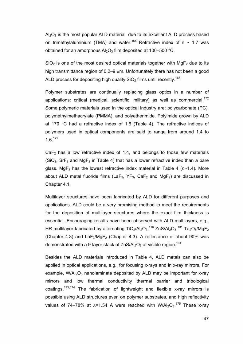
Fig. 15 Cross-sectional SEM image of a two-layer monolithically integrated half-wave plate with two fully trench-filled nanostructure grating layers.176
ALD can also be applied for shape engineering due to the conformal film growth
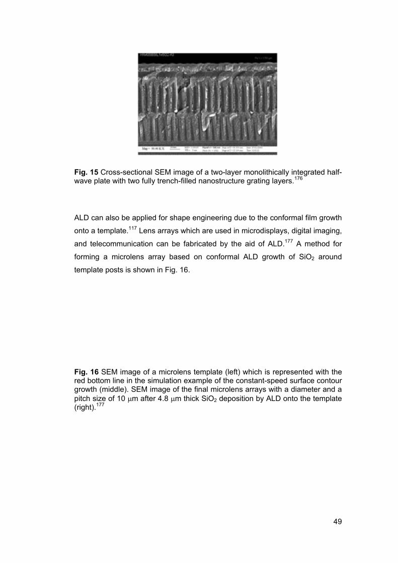
onto a template.117 Lens arrays which are used in microdisplays, digital imaging,
and telecommunication can be fabricated by the aid of ALD.177 A method for
forming a microlens array based on conformal ALD growth of SiO2 around
template posts is shown in Fig. 16.
Fig. 16 SEM image of a microlens template (left) which is represented with the red bottom line in the simulation example of the constant-speed surface contour growth (middle). SEM image of the final microlens arrays with a diameter and a pitch size of 10 �m after 4.8 �m thick SiO2 deposition by ALD onto the template (right).177
50
51
3 EXPERIMENTAL
In this chapter, the methods used for thin film growth studies and for the
characterization of the deposited films are presented. More specific information
including, when relevant, precursor synthesis, properties and pulsing
sequences can be found in the original publications (I-VII).
Film deposition
CaF2,I MgF2,II,V LaF3,III YF3,IV and Ta2O5 (Chapter 4.2) thin films were grown in
a hot-wall flow-type F-120 reactor (ASM-Microchemistry Ltd., Helsinki, Finland).
Ir thin films for inductive grid filters was also coated with the F-120 reactor,VII,178
whereas Ir films for micro channel plates as well as Fresnel zone plates were
deposited with SUNALE™ R150 reactor (Picosun, Espoo, Finland).179,VI The
pressure in both reactors was below 10 mbar. The films were mainly deposited
onto 5 × 5 cm2 Si(100,111) substrates with native SiO2. Other substrates were
2.5 × 5 cm2 quartz, 5 × 5 cm2 glass (borosilicate and sodalime), and 5 × 5 cm2
ITO (Indium tin oxide) film on glass.
Film characterization
The films were characterized by many different methods. Adhesion of the films
was tested with a simple Scotch tape test. Thicknesses and refractive indices of
the films were determined from optical reflection and transmission spectra
obtained with a Hitachi U2000 spectrophotometer in the wavelength range of
190–1100 nm. A fitting program, described elsewhere,32 was used in analyzing
the spectra. In some cases the spectra were measured with a Lambda850
spectrometer in the wavelength range of 140–800 nm.II,III
Film thicknesses, densities and crystalline structures were evaluated from X-ray
reflection (XRR) and grazing incidence X-ray diffraction (GI-XRD) patterns
measured with a PANalytical X´pert Pro MPD x-ray diffractometerIV-V or with a
52
Bruker-axs D8 Advance x-ray diffractometer.I-III
Film morphology was studied with atomic force microscopy (AFM), scanning
electron microscopy (SEM), and transmission electron microscopy (TEM) was
used only in case of MgF2 deposited from TiF4 + Mg(thd)2.II TEM studies were
done by using a JEOL JEM 3010 equipment operated at 300 kV, with a point-to-
point resolution of 0.21 nm. AFM studies were done by using a Veeco
Instrument Nanoscope V. Samples were measured in tapping mode in air using
a phosphorus doped silicon probe (RTESP) delivered by Veeco Instrument with
a scanning frequency 0.3–1.0 Hz. Roughness values were calculated as root-
mean-square values (Rq). Several wide scans were performed from different
parts of the samples to guarantee the uniformity of the film surface. Final
images were measured from a scanning area of 2 × 2 �m2 and no image
processing except flattening was done. For SEM studies a Hitachi S4800
FESEM equipment was used. The samples were coated a thin metal alloy using
a Cressington 208HR sputter coater.
Composition of the films was analyzed by time-of-flight elastic recoil detection
analysis (TOF-ERDA) using 24 MeV 127I5+,I-III and 35 MeV 34Cl7+ projectile
beam.IV-V More details from ERD analysis is found elsewhere.180
Electrical properties, permittivity and current density, were measured at room
temperature on Al/metal fluoride/ITO/glass capacitor structures with Al dot
electrode area of 2.04 x 10⁻⁷ m2. About 100 nm thick Al dots were deposited on
top of the metal fluoride films by e-beam evaporation (EBE) through a shadow
mask. Permittivity of the films was measured using a HP 4284A precision LCR-
meter at 10 kHz. A Keithley 2400 SourceMeter was used to measure leakage
current densities.
Inductive grid filters (Chapter 4.4) were done in collaboration with the University
of Joensuu (Finland). The filters were fabricated in Joensuu excluding Ir coating
made by ALD. Micro channel plates (MCPs) (Chapter 4.5) were fabricated
together with Oxford Instruments (Espoo, Finland), the University of Joensuu
(Finland), and the University of Leicester (England). Fresnel zone plates
(Chapter 4.6) were done in collaboration between the Universitat Autonoma de
Barcelona (Spain) and the Paul Scherrer Institut in Villigen (Switzerland). The

53
silicon structures were patterned in Switzerland and later scanning transmission
x-ray microscopy experiments were carried out at the PolLux Beamline of the
Swiss Light Source at the Paul Scherrer Institut.

54
55
4 RESULTS AND DISCUSSION
The main results of the thesis are summarized in this chapter. More details
about ALD processes and experimental work can be found in the corresponding
publications (I-VII).
4.1 Novel ALD processes of metal fluorides
Fluoride ALD processes have been largely missing, which is mostly due to lack
of a good fluorine precursor. TiF4I-IV and TaF5
V were applied as novel fluorine
precursors in these studies. They are both solids with relatively low vapor
pressure at room temperature and can thus be quite safely handled and
removed from reactor exhaust gases. Both fluorine sources also have the
properties required for an ALD precursor, e.g., sufficient volatility as well as high
reactivity and good thermal stability.12 It must be emphasized that it is
uncommon to use metal compound as non-metal precursor source in ALD.12, 114
Thus, the key question in these reactions is how completely the reaction can be,
i.e., how thd ligands and especially metal atoms can be eliminated from the final
film.
TiF4 precursor was used for the first time as a fluorinating agent for depositing
CaF2,I MgF2,II LaF3,III and YF3IV thin films by ALD. TaF5 was used as an
alternative novel fluorine source only for depositing MgF2 thin films.V Because of
the larger size of Ta (ionic radii of 0.64 Å) compared to Ti (0.42 Å),181 tantalum
may be less readily incorporated as an impurity into MgF2 thin films. This
decrease in metal impurities would lead to increase of desired UV light
transmittance of the films.
4.1.1 Film growth
Growth characteristics of ALD metal fluoride thin films were studied on silicon
substrates. Uncommonly high growth rates for thermal ALD processes were

56
obtained,182 especially in the case of LaF3 thin films; 1.8–5.2 Å/cycle (Fig. 17
and Table 6). Other growth rates (Å/cycle) were 0.5–1.6 for CaF2, 1.1–1.7 for
YF3, 0.7–1.6 for MgF2 (from TiF4), and 0.4–1.1 for MgF2 (from TaF5) (Fig. 17).
Fig. 17 Growth rates of fluoride thin films on Si as a function of deposition temperature.
Explanation for these high growth rates may be found from a unique film growth
mechanism. While the detailed reaction mechanism remains unidentified at the
moment, the following net reactions (1, 2) are suggested:
2 Ca(thd)2 (g) + TiF4 (g) � 2 CaF2 (s) + Ti(thd)4 (g) (1)
5 Mg(thd)2 (g) + 2 TaF5 (g) � 5 MgF2 (s) + 2 Ta(thd)5 (g) (2)
In the reaction of Ca(thd)2 and TiF4 (1), a solid CaF2 is formed as well as volatile
Ti(thd)4. With this suggested reaction (1), 4 times higher growth rate was
reached for CaF2I than that published before for ALD of CaF2 with HF as the
fluorine source.13 The same type of reaction using TiF4 as a fluorinating agent
can be applied for depositing MgF2,II LaF3,III and YF3IV thin films. Even if this
ALD process was quite general, it was not successful in all cases, for example
Al(thd)3, Gd(thd)3 and Pb(thd)2 did not react with TiF4 forming fluoride. In
reaction (2) volatile precursors form solid MgF2V and volatile Ta(thd)5.
In ALD, the overall reaction is divided into two half reactions occurring during
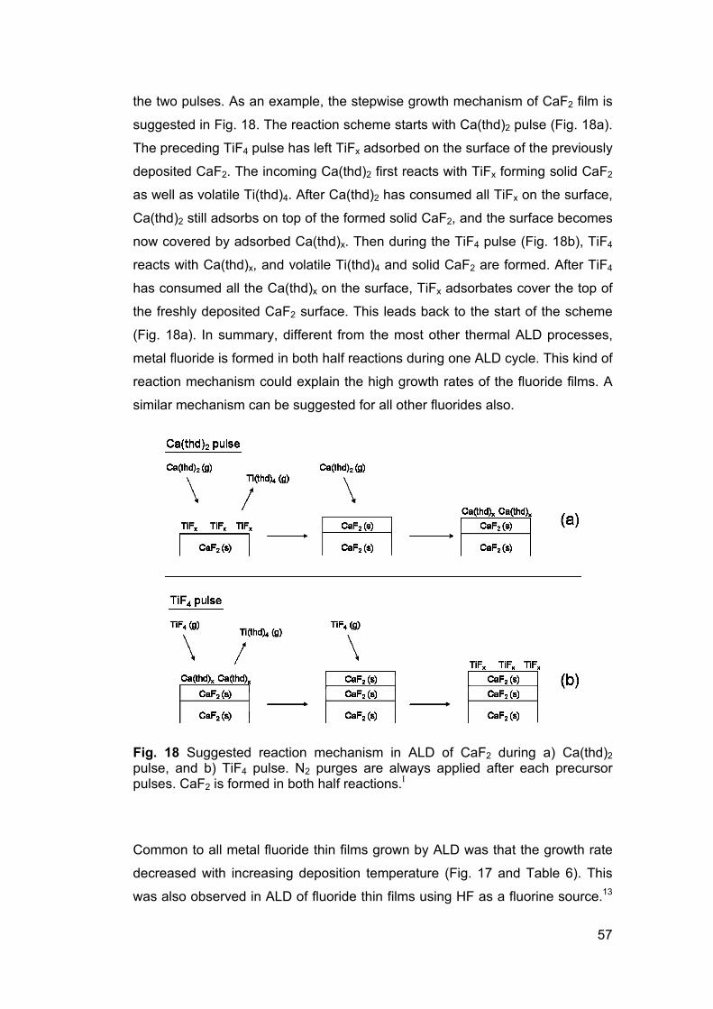
57
the two pulses. As an example, the stepwise growth mechanism of CaF2 film is
suggested in Fig. 18. The reaction scheme starts with Ca(thd)2 pulse (Fig. 18a).
The preceding TiF4 pulse has left TiFx adsorbed on the surface of the previously
deposited CaF2. The incoming Ca(thd)2 first reacts with TiFx forming solid CaF2
as well as volatile Ti(thd)4. After Ca(thd)2 has consumed all TiFx on the surface,
Ca(thd)2 still adsorbs on top of the formed solid CaF2, and the surface becomes
now covered by adsorbed Ca(thd)x. Then during the TiF4 pulse (Fig. 18b), TiF4
reacts with Ca(thd)x, and volatile Ti(thd)4 and solid CaF2 are formed. After TiF4
has consumed all the Ca(thd)x on the surface, TiFx adsorbates cover the top of
the freshly deposited CaF2 surface. This leads back to the start of the scheme
(Fig. 18a). In summary, different from the most other thermal ALD processes,
metal fluoride is formed in both half reactions during one ALD cycle. This kind of
reaction mechanism could explain the high growth rates of the fluoride films. A
similar mechanism can be suggested for all other fluorides also.
Fig. 18 Suggested reaction mechanism in ALD of CaF2 during a) Ca(thd)2 pulse, and b) TiF4 pulse. N2 purges are always applied after each precursor pulses. CaF2 is formed in both half reactions.I
Common to all metal fluoride thin films grown by ALD was that the growth rate
decreased with increasing deposition temperature (Fig. 17 and Table 6). This
was also observed in ALD of fluoride thin films using HF as a fluorine source.13

58
One explanation could be that the adsorption density of TiFx may decrease at
elevated temperature.I
4.1.2 Crystallinity and density
Because most of the films are polycrystalline, the films consist of crystalline
grains, which are separated by grain boundaries that are less dense and may
be impurity-enriched.22 This is the reason why film properties may differ
significantly from bulk properties.
Table 5. Densities and crystalline structures of fluoride thin films on Si. Densities were determined by XRR or ERDA*.
Material ALD process Growth temperature
(°C)
Density (g/cm3)
Ref. density (g/cm3)
Crystalline structure
MgF2 Mg(thd)2+TiF4II
Mg(thd)2+TaF5V
250–400
225–400
2.4–2.8
2.9–3.1
3.1530 Crystalline,
tetragonal
Crystalline,
tetragonal
CaF2 Ca(thd)2+TiF4I 300–450 2.9–3.1 3.1830 Crystalline,
cubic
LaF3 La(thd)3+TiF4III 225–350 3.3–4.5 5.930 Crystalline,
hexagonal
YF3 Y(thd)3+TiF4IV 175–200
225–325
2.6–3.8*
4.2–4.8*
5.1183 Amorphous
Crystalline,
orthorhombic

59
The trend that film density increased with the growth temperature was similar to
all fluoride films (Table 5). One reason for this might be that the films grown at
high deposition temperatures are also much purer.
Diffraction patterns of all fluorides are illustrated in Fig. 19. The following
phases were obtained: tetragonal for MgF2, cubic for CaF2, orthorhombic for
YF3, and hexagonal for LaF3. Interestingly, the most intense reflection of MgF2
film grown from TaF5 at 400 °C was (111), whereas for MgF2 film grown from
TiF4 at the same temperature it was (110) reflection. As an exception, YF3 films
could be deposited below 225 °C, and the films were amorphous when
deposited at 175–200 °C. However, YF3 thin films were polycrystalline when the
substrate temperature was 225 °C and above.
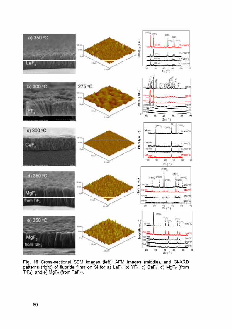
60
Fig. 19 Cross-sectional SEM images (left), AFM images (middle), and GI-XRD patterns (right) of fluoride films on Si for a) LaF3, b) YF3, c) CaF2, d) MgF2 (from TiF4), and e) MgF2 (from TaF5).

61
4.1.3 Morphology and surface roughness
The morphology of the film was analyzed by AFM and cross-sectional SEM
(Figs. 19 and 20). The growth mode of LaF3 at 350 °C is columnar (Fig. 19a),
whereas at 250 °C the structure was between columnar and granular.III
Columnar type of film growth was also observed with MgF2 samples (Fig. 19d
and e). On the other hand, YF3 seems to have lamellar type of growth at 275–
300 °C (Fig. 19b), and CaF2 grows granularly at 300 °C (Fig. 19c).
The surface roughness of the fluoride films on the silicon substrates increased
usually with an increase in the deposition temperature as seen in Table 6 and
Fig. 20. Smooth films were typically observed only at the lower growth
temperatures, but unfortunately they had also high impurity contents. MgF2 film
deposited from Mg(thd)2 and TiF4 at 400 °C and YF3 film deposited at 350 °C
had noteworthy high rms-roughness values of 23.0 and 17.0 nm, respectively.
Fig. 20 Roughness (nm) divided film thickness (nm) %-values as a function of growth temperature (°C).
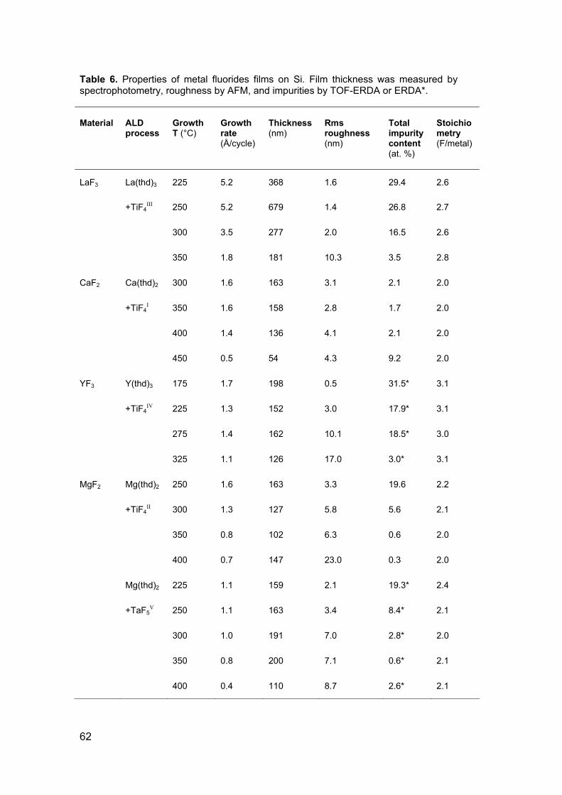
62
Table 6. Properties of metal fluorides films on Si. Film thickness was measured by spectrophotometry, roughness by AFM, and impurities by TOF-ERDA or ERDA*.
Material ALD process
Growth T (°C)
Growth rate (Å/cycle)
Thickness (nm)
Rms roughness (nm)
Total impurity content (at. %)
Stoichiometry (F/metal)
LaF3 La(thd)3 225 5.2 368 1.6 29.4 2.6
+TiF4III 250 5.2 679 1.4 26.8 2.7
300 3.5 277 2.0 16.5 2.6
350 1.8 181 10.3 3.5 2.8
CaF2 Ca(thd)2 300 1.6 163 3.1 2.1 2.0
+TiF4I 350 1.6 158 2.8 1.7 2.0
400 1.4 136 4.1 2.1 2.0
450 0.5 54 4.3 9.2 2.0
YF3 Y(thd)3 175 1.7 198 0.5 31.5* 3.1
+TiF4IV 225 1.3 152 3.0 17.9* 3.1
275 1.4 162 10.1 18.5* 3.0
325 1.1 126 17.0 3.0* 3.1
MgF2 Mg(thd)2 250 1.6 163 3.3 19.6 2.2
+TiF4II 300 1.3 127 5.8 5.6 2.1
350 0.8 102 6.3 0.6 2.0
400 0.7 147 23.0 0.3 2.0
Mg(thd)2 225 1.1 159 2.1 19.3* 2.4
+TaF5V 250 1.1 163 3.4 8.4* 2.1
300 1.0 191 7.0 2.8* 2.0
350 0.8 200 7.1 0.6* 2.1
400 0.4 110 8.7 2.6* 2.1

63
4.1.4 Composition
Good stoichiometry as well as purity of fluoride films is important because
impurities increase absorbance of the film, especially in the UV range.
Contamination becomes more important in the VUV where the extinction
coefficients of water and of most organic compounds are higher by orders of
magnitude compared to the visible spectral range.26 CaF2 thin films had a good
stoichiometry with F/Ca ratio value of 2.0 in all the films grown in the
temperature range of 300–450 °C (Table 6). LaF3 thin films were fluorine
deficient with F/La ratio of 2.6–2.8. However, these ratios were still closer to
stoichiometric than those reported for some PVD methods,184,185 which shows
that LaF3 films with exact stoichiometry are difficult to reach. YF3 thin films had
F/Y ratios between 3.0 and 3.1, whereas MgF2 thin films deposited from
Mg(thd)2 + TiF4 had F/Mg ratios of 2.0–2.2. On the other hand, MgF2 films
grown using TaF5 as a fluorinating agent were slightly fluorine rich with F/Mg
ratio between 2.0 and 2.4.
Total impurity contents in the films seem to decrease with increasing substrate
temperature, except for CaF2 films (Table 6). The impurity content of CaF2
stayed around 2.0 at. % at 300–400 °C, but due to decomposition of the
Ca(thd)2 precursor at 450 °C the content increased up to 9.2 at. %. At lower
deposition temperatures, especially in the case of LaF3 (225–250 °C) and YF3
(175 °C) samples, a lot of impurities were detected with total values around 30
at. %. High amounts of impurities could be caused by a incomplete reaction.
High growth rates of these films also support that conclusion. The lowest total
impurity contents (at. %) were usually obtained at higher growth temperatures:
1.7 for CaF2 at 350 °C, 0.6 for MgF2 grown from TaF5 at 350 °C, 0.3 for MgF2
grown from TiF4 at 400 °C, 3.5 for LaF3 at 350 °C, and 3.0 for YF3 at 325 °C.
Metal/F ratio was improved especially for MgF2 thin films when the total impurity
content decreased. The detected impurities were H, C, O and Ti or Ta
depending on the used fluorine source. Unfortunately the highest purity was
correlated with the poorest morphology in the YF3 and MgF2 samples.

64
4.1.5 Optical properties
It should be kept in mind that the depositions and characterizations of the films
in this thesis have not been done in clean room environment, which might have
affected the light transmittance of the films caused by impurity particles. In
addition, the optical as well as other properties of thin films differ from the pure
bulk materials. For example, the transparency of vacuum deposited thin films is
often slightly worse than that of bulk materials.21 A small packing density causes
a reduction of the refractive index of the films. Light transmittance depends
heavily on the impurities; especially in the UV range.40 Measuring the
absorption is a straightforward way to confirm the purity of the film.
Generally the refractive indices were close to the bulk values at the visible
region (Table 7). However, lower than the bulk values were obtained at higher
deposition temperatures. This is mainly due to increasing roughness and
porosity of the polycrystalline film microstructure,186 as shown by SEM and AFM
(Fig. 19). Generally the absorption for the fluoride films was negligible, except
for YF3 films the absorption coefficients of 0–500 cm-1 were obtained (� = 1.0
�m). Therefore, slightly higher than bulk indices were observed at lower growth
temperatures caused by high amount of impurities, especially oxygen in YF3
films.
The transmittance curves were measured down to 190 nm only from films
having a combination of high purity with reasonably low roughness. For these
measurements the films were deposited onto high transmittance quartz
substrates. Comparisons made with YF3IV and MgF2
II,V showed that the purer
film grown at higher temperature seemed to be better choice. Only the highest
transmittance samples of these are illustrated in Fig. 21. The highest
transmittances were obtained with MgF2 films due to their low total impurity
contents of 0.6 at. % (Table 6). MgF2 and CaF2 have lower refractive indices
than the bare quartz substrate; therefore, their transmittance curves are above
the quartz curve (Fig. 21). MgF2 thin film deposited from Mg(thd)2 + TaF5 onto
quartz substrate had the highest light transmittance down to the UV region. This
proves that TaF5 must be considered as an excellent fluorine source for ALD,
and even better than TiF4. On the other hand, YF3/quartz sample had the
weakest light transmittance in the near UV region. This is mainly due to light

65
absorption by high amount of impurities, as discussed already above. However,
YF3 had the reasonable light transmittance at 500–1100 nm.
Table 7. Refractive indices of fluoride thin films on Si determined by spectrophotometry.
Material ALD process Growth temperature
(°C)
Refractive
index n (� =
580 nm)
Ref. refractive
index n (� =
589 nm)
LaF3 La(thd)3+TiF4III 225–350 1.58–1.61 1.6130
YF3 Y(thd)3+TiF4IV 175–325 1.51–1.59 1.55183
CaF2 Ca(thd)2+TiF4I 300–450 1.42–1.44 1.4330
MgF2 Mg(thd)2+TiF4II
Mg(thd)2+TaF5V
250–400
225–400
1.34–1.42
1.36–1.38
1.3830

66
Fig. 21 Transmittance spectra of metal fluoride thin films on quartz, and a spectrum of bare quartz substrate in a wavelength range of 190–1100 nm. Film thicknesses were 100 nm for MgF2 (from TaF5), 155 nm for MgF2 (from TiF4), 143 nm for CaF2, 110 nm for LaF3, and 127 nm for YF3.
4.1.6 Electrical properties
Metal fluorides are dielectric materials with high band gap values of (eV): 12.8
for MgF2,187 12.1 for CaF2,52 10.3 for YF3,188 and 10.3 also for LaF3.189 Electrical
behaviour of the metal fluoride thin films was measured from Al/fluoride/ITO
capacitor structures on glass and results are introduced in Table 8.
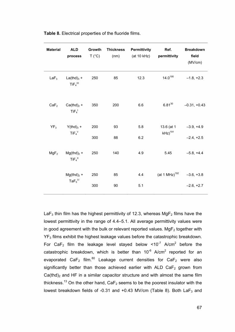
67
Table 8. Electrical properties of the fluoride films.
Material ALD process
Growth
T (°C)
Thickness
(nm)
Permittivity
(at 10 kHz)
Ref. permittivity
Breakdown field
(MV/cm)
LaF3 La(thd)3 +
TiF4III
250 85 12.3 14.0190 –1.8, +2.3
CaF2 Ca(thd)2 +
TiF4I
350 200 6.6 6.8130 –0.31, +0.43
YF3 Y(thd)3 +
TiF4V
200
300
93
88
5.8
6.2
13.6 (at 1
kHz)191
–3.9, +4.9
–2.4, +2.5
MgF2 Mg(thd)2 +
TiF4II
250 140 4.9 5.45 –5.8, +4.4
Mg(thd)2 +
TaF5IV
250
300
85
90
4.4
5.1
(at 1 MHz)192 –3.6, +3.8
–2.6, +2.7
LaF3 thin film has the highest permittivity of 12.3, whereas MgF2 films have the
lowest permittivity in the range of 4.4–5.1. All average permittivity values were
in good agreement with the bulk or relevant reported values. MgF2 together with
YF3 films exhibit the highest leakage values before the catastrophic breakdown.
For CaF2 film the leakage level stayed below <10-7 A/cm2 before the
catastrophic breakdown, which is better than 10-6 A/cm2 reported for an
evaporated CaF2 film.80 Leakage current densities for CaF2 were also
significantly better than those achieved earlier with ALD CaF2 grown from
Ca(thd)2 and HF in a similar capacitor structure and with almost the same film
thickness.13 On the other hand, CaF2 seems to be the poorest insulator with the
lowest breakdown fields of -0.31 and +0.43 MV/cm (Table 8). Both LaF3 and

68
YF3 thin films had leakage levels below 10-5 A/cm2 before the breakdowns.
MgF2 film deposited from TiF4 had high breakdown fields of -5.8 and +4.4
MV/cm, which are incredibly better than 0.2 MV/cm observed earlier for a 292
nm thick MgF2 film deposited by thermal evaporation.80 Anyhow, MgF2 film
grown using TiF4 as a fluorine precursor had a leakage level below <10-5 A/cm2
before breakdown, whereas MgF2 films grown from TaF5 at 250 and 300 °C had
lower leakage levels of 10-8 A/cm2 and 10-7 A/cm2 before breakdown,
respectively. And as expected, YF3 film with the amorphous film structure
(Table 5) grown at 200 °C is a better insulator (-3.9 and +4.9 MV/cm) than the
highly crystalline 300 °C sample (-2.4 and +2.5 MV/cm) where the current can
leak along the grain boundaries. The leakage current density stayed below 10-5
A/cm2 within both samples before the breakdown.
In a summary, results in Table 8 prove that most ALD grown metal fluoride films
remain in the class of good insulators, despite polycrystalline structure of these
films (Table 10).
4.2 High reflecting coating / bandpass filter
To study the applicability of the new fluoride processes in fabricating of high
reflecting optical coating, the multilayer stack was built up from quarter-wave
layers of MgF2 and Ta2O5 for visible region, and another stack of MgF2 and
LaF3 for UV region. Reflection over as high as 99% can be achieved in narrow
bands with quarter-wave stacks, which exhibit very low absorption, and
therefore are qualified for high-energy laser applications.34
It has been shown already that ALD can be applied in preparation of multilayer
stack for optical applications.131 However, multilayer stack of oxide and fluoride
films or just fluoride films has never been fabricated by ALD. It is an interesting
and difficult task; alternating oxide and fluoride coatings can be problematic
because oxygen must be present for the oxide compound but, simultaneously,
oxygen incorporation or substitution in the fluoride layer must be avoided to
maintain low optical absorption.193

69
The multilayer coatings were built up from quarter-wave layers so that the
layers had optical thicknesses:
nd=�/4 (23)
where n is refractive index of the layer, and d is the geometric thickness of the
layer. The wavelength � was chosen to be 550 nm at visible region and 248 nm
for UV region.
Visible region. High reflecting (HR) coating for visible area were grown by ALD
using Ta2O5 as a high-n (H) and MgF2 as a low-n (L) material. Their
combination provides a high index ratio, and thereby a minimum number of
layers required to achieve a desired performance. Ta2O5 was deposited from
Ta(OEt)5 and H2O, whereas MgF2 was grown from Mg(thd)2 and TaF5. The
deposition temperature was 250 ºC. Refractive indices determined from test
ALD runs were 2.18 for Ta2O5 and 1.42 for MgF2. When using these refractive
indices, values of 67 nm for Ta2O5 and 97 nm for MgF2 were evaluated for the
geometric thicknesses from Eq. 25. Once the exact growth rates were
determined from the test ALD runs, the numbers of deposition cycles were
chosen so that the target film thicknesses could be achieved. The optical
performance was examined by comparing the measured reflectance spectrum
with that calculated for the ideal design structure.
A reflectance spectrum of nine-layer structure (HLHLHLHLH) is depicted in Fig.
22. This kind of structure acts as a HR coating as discussed above. The main
interest lies in the HR region of 450–720 nm. The side band regions where the
reflectance exhibits several maxima and minima are not that important. The
measured reflectance was about 96%, whereas the design reflectance was
97%. Higher reflectance could be obtained by just simply depositing more
layers. As shown in Fig. 22 (left), the measured curve (squares) has been
slightly shifted to longer wavelengths than the design curve (solid line). A
reason for this is that the growth rate of MgF2 was slightly more than estimated
from the test run. However, as illustrated in Fig. 22 (right), fitted curve (dashed
line) with increased thickness of MgF2 layers it fit properly together with the
measured one (squares). Due to the increased thickness of the MgF2 layers (97
nm � 103 nm), 1% of the reflectance is lost from 97% to 96% at the same time.

70
Fig. 22 Designed (solid line), measured (squares), and fitted (dashed line) reflectance spectra of a nine-layer structure HLHLHLHLH/glass. H is Ta2O5 film and L is MgF2.
Fig. 23 GI-XRD patterns (left) and AFM image (right) of HLHLHLHLH structure grown onto silicon (AFM image, right) or glass at 250 °C. H is Ta2O5 film and L is MgF2.
Crystalline structure of the stack structure was measured as well as the surface
roughness (Fig. 23). Ta2O5 grown from Ta(OEt)5 and H2O at 250 °C stays
amorphous, whereas MgF2 is polycrystalline. Rms-roughness of the 9-layer
sample was only 2.7 nm.
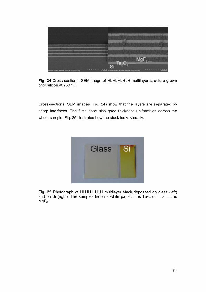
71
Fig. 24 Cross-sectional SEM image of HLHLHLHLH multilayer structure grown onto silicon at 250 °C.
Cross-sectional SEM images (Fig. 24) show that the layers are separated by
sharp interfaces. The films pose also good thickness uniformities across the
whole sample. Fig. 25 illustrates how the stack looks visually.
Fig. 25 Photograph of HLHLHLHLH multilayer stack deposited on glass (left) and on Si (right). The samples lie on a white paper. H is Ta2O5 film and L is MgF2.

72
UV region. The same design was used for preparing four-layer HR stack for UV
region. This time instead of use of Ta2O5, LaF3 was used as a high-n material
(H) due to its better UV light transmittance. LaF3 was deposited by using
La(thd)3 and TiF4 as precursors, whereas MgF2 (L) was grown from Mg(thd)2
and TiF4. The deposition temperature was 275 ºC. 248 nm was chosen as a
central wavelength. Refractive indices determined from test ALD runs were 1.62
for LaF3 and 1.43 for MgF2. With these refractive indices, values of 38 nm for
LaF3 and 43 nm for MgF2 were evaluated for the geometric thicknesses from
Eq. 23, (Table 9).
Table 9. Film thicknesses and refractive indices used for LaF3 and MgF2 films in reflectance spectra (Fig. 44).
Material Design Fitted
d (nm) n (580 nm) d (nm) n (580 nm)
LaF3 38 1.62 35 1.60
MgF2 43 1.43 36 1.40
LaF3 38 1.62 35 1.60
MgF2 43 1.43 39 1.40

73
A reflectance spectrum of four-layer structure (HLHL) on silicon is depicted in
Fig. 26. This time the main interest lies in the HR region of around 190–250 nm.
The measured reflectance (squares) as well as the ideal design (solid line) was
about 80% (Fig. 26). Higher reflectance could be obtained by just simply
depositing more layers. As illustrated in Fig. 26 left, the measured curve has
been shifted to shorter wavelengths than the designed one (solid line) because
the growth rates of the fluorides as well as the refractive indices were slightly
less than determined from the test runs. However, fitted curve (dashed line),
which used parameters are shown in Table 9, fits together with the measured
curve, as shown in Fig. 26 right. Even the reflectance stayed around 80%.
Fig. 26 Designed (solid line), measured (boxes), and fitted (dashed line) reflectance spectra of a four-layer structure HLHL/Si. H is LaF3 film and L is MgF2.

74
4.3 Anti-tarnishing coating
To show that ALD method can also be used for protecting silver mirror coatings
a thin film of Al2O3 was deposited by ALD on top of a 100 nm thick Ag film
evaporated by e-beam. 5 x 5 cm2 glasses were used as substrates in this
experiment. About 5 nm thick Al2O3 film was fabricated from TMA and H2O
precursors at 250 °C. A reference Ag/glass sample was also heated in the
same ALD reactor at 250 °C for the same time as the ALD process took place,
but of course without ALD coating. Since then the samples have been aged for
three years and 10 months in normal room atmosphere (Fig. 27). Silver mirror
coating with Al2O3 film is still bright, but the Ag layer without protective thin film
is tarnished. This experiment simply shows that the ALD method has potential
for depositing anti-tarnishing films and could especially be applied for
components with complex shapes and topographies.
Fig. 27 Photo of already tarnished Ag/glass (left), and bright Al2O3/Ag/glass (right). The samples have been aged almost four years at room atmosphere. Mirrors show Finnish cloudy summer sky taken with a digital camera without flash and the photo has not been processed in any way.

75
4.4 Inductive grid filters
The fabrication process of a freestanding inductive grid filter prototype for
rejecting IR light is presented here.VII The idea of the inductive grid filter is
simple: it behaves like a metal grid in a door of a microwave oven that passes
shorter visible light through but keeps longer harmful microwaves inside the
oven. This concept is widely used also in the mirrors of radio telescopes. For
rejecting microwave radiation, the grid structures or holes need only be on the
order of one decimetre, but for rejecting IR radiation, the fabricated structures
have to be scaled down in submicron size. Inductive grid filters are aimed to be
used in front of x-ray detectors that will operate at cryogenic temperatures in
space and should be protected from IR radiation to avoid heating.
The thickness of the grid affects the absorption of IR radiation, while the
effective area of the holes of the grid is responsible for the transmission in the
short wavelength region. To allow x-rays to pass through the filter, the metal
grid must be freestanding and supported only by its edges, otherwise x-rays
would be blocked by the substrate.
Development of inductive grid filters has been challenging and a few techniques
have been tried out for fabricating these filters. The inductive grid fabrication
process steps starting from Si wafer substrate and finishing to freestanding Ir
grid are schematically shown in Fig. 28. Briefly, Si substrate was covered with
layers of SiNx, Cr, SiO2, PMMA, and Cu (Fig. 28 A). After that the grid filter was
manufactured with low energy electron beam lithography (B), etching (C), Ir-
coating of deep grooves by ALD using Ir(acac)3 and O2 precursors at 300 °C
(D), etching again (E-F), and removing etch stop layers (G) and the mask (H).
The final grid structure after preparation was: period of 400 nm, linewidth of ~80
nm, and thickness of ~400 nm. More details about the manufacturing process
are found in the corresponding article (VII).
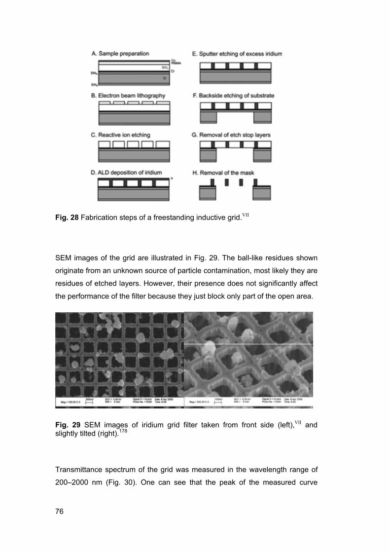
76
Fig. 28 Fabrication steps of a freestanding inductive grid.VII
SEM images of the grid are illustrated in Fig. 29. The ball-like residues shown
originate from an unknown source of particle contamination, most likely they are
residues of etched layers. However, their presence does not significantly affect
the performance of the filter because they just block only part of the open area.
Fig. 29 SEM images of iridium grid filter taken from front side (left),VII and slightly tilted (right).178
Transmittance spectrum of the grid was measured in the wavelength range of
200–2000 nm (Fig. 30). One can see that the peak of the measured curve

77
(dashed) is lower and slightly shifted towards longer wavelengths than
calculated curve (solid). This is mainly caused by the ball-like residuals on top
of the filter (Fig. 29). Calculation of the transmittance curve is beyond this thesis
and can be found in more details elsewhere.VII The correspondence between
experimental and theoretical results is not perfect; still it represents relatively
high rejection of the IR light. In the IR region the transmittance reduces strongly
and is only 0.5% at 2000 nm. In the visible region the transmittance curve
reaches a peak, around 34% at 540 nm. Going down to the shorter wavelengths
absorption of the metal continues to increase, which leads to a decrease of the
transmittance. The transmittance could not be measured in the region of 1–100
nm, but a transmittance of 40% was calculated with the same parameters as
used in Fig. 30.
Fig. 30 Calculated (solid curve) and measured (dashed) zeroth order transmittance spectra of a free-standing Ir grid with the following parameters: period of 400 nm, linewidth of ~80 nm, and thickness of ~400 nm.VII
As a conclusion, a method for fabrication of a freestanding grid filter for IR
radiation rejection was developed. The first freestanding iridium grid filter
prototype was fabricated and it was capable of suppressing IR radiation by a
factor of 100 while keeping the transmittance in the x-ray region at around 40%.
Unfortunately, the fabrication method is quite unique and difficult, which makes
it hardly repeatable. However, ALD was successful in its part; the problems
were in other fabrication steps.

78
4.5 Micro channel plates
In this section, micro channel plates (MCPs) used for focusing x-rays are shortly
introduced. MCPs are made from a matrix of hollow glass tubes fused together.
Normally the MCPs have circular channels, typically 5 �m to 12 mm in diameter,
but for the x-ray optics purposes square type of channels are mostly used
because of better filling factor. MCPs are planned to be applied in the optics of
imaging x-ray fluorescence spectrometer MIXS onboard of European Space
Agency’s BepiColombo Mercury Orbiter to be launched in 2013.179 Fluorescent
x-rays that come from the surface of Mercury to the curved MCPs, are reflected
by the metal coated channel walls, and thereby focused onto a detector. The
device mimics the eye of a lobster where millions of micro channels focus the
light (Fig. 31). The advantage of the MCP optics is that it is much lighter than
the more conventional x-ray optics.
Fig. 31 Left: The eye of a lobster, viewed with a microscope. Right: close-up image of a small area of the eye. The eye consists of millions of square “channels”, each channel measure about 20 microns across.194
The performance of x-ray mirrors is severely limited when the grazing angle is
greater than a few degrees or when the energy of x-ray is greater than 2 keV.
This applies also to MCP based x-ray optics so that the efficiency at larger
grazing angle or at higher energy can be increased by coating the MCPs with
metal layers of a high density, and thus with a high critical angle for total
reflection of x-rays. But producing smooth and conformal coating inside the

79
pores is a difficult task for, e.g., sputtering because the metal does not
penetrate deep in the holes in this method. Fortunately, conformal metal film
with high density might be deposited by the ALD technique, but it is still a big
challenge because of the long and narrow channels.
Fig. 32 Schematic picture of the novel flow through type ALD reactor.195
Fig. 33 Photos of un-coated (left) and Ir-coated (right) MCPs. One euro coin is just shown as a reference.179
The MCPs test samples with 20 �m square pores were up to 2.8 mm thick with
a size of about 10 x 10 mm2, so aspect ratios were up to 140:1. The MCPs were
coated with about 10–20 nm of Ir metal by ALD in a SUNALE™ (Picosun,
Espoo, Finland) reactor at 350 °C using the novel reactor geometry where the
precursors are forced to flow through the porous substrate (Fig. 32). About 1 nm

80
thick Al2O3 film, deposited by ALD from TMA and water, was used as a seed
layer. The metal precursors were Ir(acac)3 and O2. The normal pulse times were
2×1.5 s for Ir and 0.7 s for oxygen with purging times of up to 120 s. Ir(acac)3
pulses were doubled to ensure sufficient amount of Ir-precursor. A special
sample holder with two or three places for the samples was used. One
challenge is to seal the MCPs well enough that no bypass routes are available
around the MCP. Reference Si pieces were placed above and under the
through-porous samples to confirm Ir thicknesses by XRR.
The MCPs were successfully coated with Ir thin film as shown in Fig. 33. Ir film
thickness was measured from a cross-section of MCP by energy dispersive x-
ray spectroscopy (EDX) (Fig. 34). Ir was found to be slightly thicker at top (17
nm) compared to the bottom of the channel (13 nm), but this is believed not to
attenuate reflectivity of the Ir-coated channels.
Fig. 34 The cross-sectional SEM image of Ir-coated MCP, insert illustrated also SEM image of top of the MCP.179
Fig. 35 The Ir-coated MCP seems visually opaque (left), but when the flashlight behind the MCP is on (right), the light can clearly pass through the channels of the MCP.
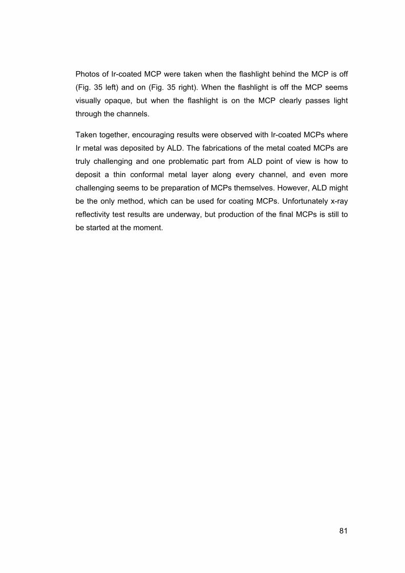
81
Photos of Ir-coated MCP were taken when the flashlight behind the MCP is off
(Fig. 35 left) and on (Fig. 35 right). When the flashlight is off the MCP seems
visually opaque, but when the flashlight is on the MCP clearly passes light
through the channels.
Taken together, encouraging results were observed with Ir-coated MCPs where
Ir metal was deposited by ALD. The fabrications of the metal coated MCPs are
truly challenging and one problematic part from ALD point of view is how to
deposit a thin conformal metal layer along every channel, and even more
challenging seems to be preparation of MCPs themselves. However, ALD might
be the only method, which can be used for coating MCPs. Unfortunately x-ray
reflectivity test results are underway, but production of the final MCPs is still to
be started at the moment.
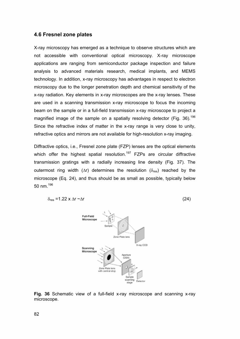
82
4.6 Fresnel zone plates
X-ray microscopy has emerged as a technique to observe structures which are
not accessible with conventional optical microscopy. X-ray microscope
applications are ranging from semiconductor package inspection and failure
analysis to advanced materials research, medical implants, and MEMS
technology. In addition, x-ray microscopy has advantages in respect to electron
microscopy due to the longer penetration depth and chemical sensitivity of the
x-ray radiation. Key elements in x-ray microscopes are the x-ray lenses. These
are used in a scanning transmission x-ray microscope to focus the incoming
beam on the sample or in a full-field transmission x-ray microscope to project a
magnified image of the sample on a spatially resolving detector (Fig. 36).196
Since the refractive index of matter in the x-ray range is very close to unity,
refractive optics and mirrors are not available for high-resolution x-ray imaging.
Diffractive optics, i.e., Fresnel zone plate (FZP) lenses are the optical elements
which offer the highest spatial resolution.197 FZPs are circular diffractive
transmission gratings with a radially increasing line density (Fig. 37). The
outermost ring width (�r) determines the resolution (�res) reached by the
microscope (Eq. 24), and thus should be as small as possible, typically below
50 nm.196
�res =1.22 x �r ~�r (24)
Fig. 36 Schematic view of a full-field x-ray microscope and scanning x-ray microscope.

83
Fig. 37 Fresnel zone plates as a diffracting element.198
Fig. 38 Zone-doubling technique of FZP. Resolution is doubled and the manufacturing is much easier. Si operates as low-n (blue) and Ir as high-n material (orange).
There has been little progress in reducing outermost zone widths over the past
ten years. This is related to an intrinsic limitation of e-beam lithography, which is
the main technique to create practically all these FZPs worldwide. While
lithography tools are capable of writing with nanometres spot sizes, the range of
secondary electrons created in the resist layer determines the obtainable
structure sizes. The exposed pattern is thus blurred, which has a particularly
detrimental consequence when writing dense patterns of lines such as gratings
or FZPs. While isolated line widths down to 10 nm can be obtained by high
resolution e-beam lithography, writing the periodic structures seems to be

84
limited to pitches of around 40–50 nm. As a consequence, no FZPs with lines
and spaces below 20–25 nm can be written in a straightforward way, and the
smallest lines resolved are 15 nm wide.197
We have developed a novel technique for a fabrication of ultrahigh resolution
FZP lenses,VI which is based on the coating of a template structure with a metal
layer of iridium (Fig. 38). The template was fabricated from single silicon crystal,
which serves as a low-n material (Fig. 38A). As Ir has a much higher x-ray
refractive index than Si, a doubling of the effective zone density and subsequent
improvement of the resolution by a factor of two compared to the template
structure is achieved (Fig. 38B). Manufacturing steps of FZP are introduced in
Fig. 39. The method is very reproducible as it only requires a single lithography
step and allows the fabrication of structures with quite high aspect ratios, which
increases the efficiency of ultrahigh resolution optics. Low voltage e-beam
lithography and a highly anisotropic reactive ion etch process were applied to
fabricate the silicon template structure (Fig. 39, 1–3). The height of the template
was 170 nm. Finally a highly conformal 20 nm thick Ir thin film was deposited by
ALD onto the template (Fig. 39, 4) using Ir(acac)3 and O2 as precursors at 350
ºC.199 The method was used to fabricate Ir-coated FZPs with line widths down
to 15 nm. A successfully fabricated FZP is shown in Fig. 40.

85
Fig. 39 Manufacturing steps of Ir-silicon Fresnel zone plate. The silicon template had 80 nm periods and a duty cycle of 0.25 at the outer regions. Finally a 20 nm thick Ir layer was deposited by ALD.198
Fig. 40 A cross-sectional SEM image of a Ir Fresnel zone plate with 20 nm wide outermost zones prepared by depositing Ir by ALD onto a silicon template. A thin Pt layer was locally deposited to achieve a clean focused ion beam cross section.VI
Fig. 41 Scanning x-ray microscope image of a test object consisting of a cross section of a GaAs/InGaAs structure with line pairs from 40 nm to down 9 nm thicknesses (left). Lines and spaces down to 12 nm can be resolved. Horizontal cross section through the image (right) shows the separation of 12 nm lines. Photon energy of 1 keV was used.

86
The imaging properties of the devices were experimentally tested in a scanning
x-ray microscope using another FZP as a test object. A resolution of 15 nm was
achieved. More recently, a test object consisting of a cross section of
GaAs/InGaAs structure was imaged. The structure consisted of layer pairs of 40
nm down to 9 nm in thickness, each separated by a spacer of the same
thickness (Fig. 41, left). Line pairs down to 12 nm could be resolved (Fig. 41,
right), which represents the best resolution achieved to date in x-ray
microscopy. However, the method still has a potential to push the limits of x-ray
microscopy even down to the sub-10 nm level, and these studies are currently
in progress.

87
88

89
5 SUMMARY AND CONCLUSIONS
Thin films of various metal fluorides can be applied in many optical applications
due to their excellent light transmission in a broad wavelength area. The
problem in depositing fluoride films by ALD has been a lack of good fluorinating
agent. Several ALD processes were developed to deposit metal fluoride thin
films from metal-thd compounds and novel fluorinating agents of TiF4 and TaF5
at 175–450 °C. The fluoride films of MgF2, LaF3 and YF3 were deposited for the
first time by ALD. In addition, for CaF2 a four times higher growth rate was
obtained than that published for ALD of CaF2 with HF as the fluorine source.
Especially MgF2 is a desired film material worldwide due to its low refractive
index and high light transmittance down to vacuum UV region. Therefore,
among the fluorides deposited the highest transmittances as well as the lowest
refractive indices below 1.4 ��=580 nm) were obtained with MgF2 samples.
MgF2 grown from the TaF5 precursor showed even better light transmittance at
UV region than MgF2 grown from TiF4. Therefore, TaF5 must be considered as
a high quality fluorine precursor for depositing fluoride thin films. Most fluoride
thin films were reasonable insulators despite their polycrystalline structure. The
highest permittivity of 12 was obtained for LaF3, whereas MgF2 films grown from
TiF4 had the highest breakdown fields.
Metal fluoride films were also used for fabricating high reflectance dielectric
mirrors. Stack samples were fabricated by deposition of a 9-layer structure with
alternating high-n Ta2O5 and low-n MgF2 films, and a 4-layer structure of LaF3
and MgF2 films. In both cases the layers were separated by sharp interfaces
and had good uniformities across the substrates. Therefore high reflectance of
96% (��= 570 nm) was obtained with Ta2O5/MgF2 sample. This proves that the
novel ALD fluoride processes can be applied also together with oxides in
multilayer structures, and higher reflectance is achievable by just depositing
more layers into the stack.
It was also shown that a thin ALD Al2O3 film could be applied as an anti-
tarnishing layer on top of the silver mirror coating. The sample was aged at
90
normal room atmosphere for almost 4 years without visible tarnishing.
One aim of this thesis was to fabricate novel optical devices. The first
freestanding iridium grid filter prototype for rejection of infrared light was
fabricated and characterized successfully. Unfortunately, the fabrication method
is difficult, which makes it hardly repeatable, but ALD was successful in its part.
Micro channels plates (MCPs), which are applied for focusing x-rays, were Ir-
coated effectively by ALD. The ALD technique might be the only method to
deposit a conformal, highly reflective metal layer onto the narrow channels of
the MCP. There is still place for an improvement to obtain highly uniform ALD
coating along the channels. However, production of the final MCPs is to be
started at the moment and hopefully they will have a safe trip to Mercury.
A novel technique was developed to fabricate Fresnel zone plates (FZPs) that
frees us from the present limitations of e-beam lithography and thereby
simplifies FZP preparation and improves the spatial resolution of x-ray
microscopy. Line pairs down to 12 nm could be resolved with the Ir-coated FZP,
which represents the best resolution achieved up to date in x-ray microscopy.
However, the method has a potential to push the resolution limits of x-ray
microscopy even down to the sub-10 nm level.
Developments in optical coating materials, deposition techniques, process
parameter control and equipment are continuing processes. Therefore, novel
coating materials and optical devices will definitely be seen in the near future.
For example, ALD of artificial fluoride materials with amorphous structure or
tailored refractive index will be the future task. Anyhow, the aims of this thesis
were achieved successfully. The novel ALD processes were introduced to
deposit fluoride thin films, which can be applied in fabrication of high reflecting
mirrors. In addition to the novel fluoride thin films, power of ALD was shown for
protecting silver mirror coating from tarnishing. Also novel devices for x-ray
optics, like grid filters and MCPs, were successfully developed. Finally,
receiving the happy end to the book, the best spatial resolution was achieved
up to date in x-ray microscopy with the Ir-coated Fresnel zone plate.

91

92
93
6 REFERENCES
(1) CERAC Inc. CERAC Coat. Mater. News 2002, 12, 2; http://www.cerac.com./pubs/CMNarchives.htm.
(2) Wang, J., Maier, R., Dewa, P. G., Schreiber, H., Bellman, R. A.; Elli, D. D. Appl. Opt. 2007, 46, 3221.
(3) Chindaudom, P.; Vedam, K. Appl. Opt. 1994, 33, 2664.
(4) Rysanek, V. Z. Appl. Opt. 1965, 4, 993.
(5) Kaiser, U., Adamik, M., Safran, G., Barna, P. B., Laux, S.; Richter, W. Thin Solid Films 1996, 280, 5.
(6) Pellicori, S. F.; Colton, E. Thin Solid Films 1992, 209, 109.
(7) Martin, P. J., Sainty, W. G., Netterfield, R. P., McKenzie, D. R., Cockayne, D. J. H., Sie, S. H., Wood, O. R.; Craighead, H. G. Appl. Opt. 1987, 26, 1235.
(8) Lee, S. E., Choi, S. W.; Yi, J. Thin Solid Films 2000, 376, 208.
(9) Fujihara, S., Tada, M.; Kimura, T. Thin Solid Films 1997, 304, 252.
(10) Suntola, T. Thin Solid Films 1992, 216, 84.
(11) Leskelä, M.; Ritala, M. Thin Solid Films 2002, 409, 138.
(12) Ritala, M.; Leskelä, M. in Handbook of Thin Film Materials; Academic Press: San Diego, 2001.
(13) Ylilammi, M.; Ranta-aho, T. J. Electrochem. Soc. 1994, 141, 1278.
(14) Ryer, A. in The light measurement handbook, International light, Newburyport, USA 1997, 1.
(15) "Optical properties of selected elements", in CRC Handbook of Chemistry and Physics, Internet Version 2007, (87th Edition), David R. Lide, ed., Taylor and Francis, Boca Raton, FL.
(16) Medintz, I. L., Uyeda, H. T., Goldman, E. R.; Mattoussi, H. Nature Mater. 2005, 4, 435.
(17) Saslow, W. M. in Electricity, magnetism, and light, Academic Press, Toronto, Canada, 2002, pp. 630-735.
(18) Yulin, S. in Optical interference coatings, Springer, Berlin, Springer series in optical sciences, Eds.: Kaiser , N. and Pulker, H.K., Vol 88, 2003, pp. 281-307.

94
(19) "Optical properties of selected inorganic and organic solids", in CRC Handbook of Chemistry and Physics, Internet Version 2007, (87th Edition), David R. Lide, ed., Taylor and Francis, Boca Raton, FL.
(20) Macleod, H. A. in Thin-film optical filters, 3rd edition, Ed.W.T. Welford, Institute of physics publishing, 2002, 1.
(21) Pulker, H. K. Appl. Opt. 1979, 18, 1969.
(22) Kaiser, N. in Optical interference coatings, Springer, Berlin, Springer series in optical sciences, Eds.: Kaiser , N. and Pulker, H.K., Vol 88, 2003, pp. 59-80.
(23) Tilley, R. J. D. in Understanding solids: the science of materials, John Wiley & Sons, Chichester, England, 2004.
(24) Coult, D. G. in Ceramic films and coatings, Ed. Wachtman, J.B., Haber, R.A., Noyes publications, New Jersey, USA 2001.
(25) Ristau, D. in Optical interference coatings, Springer, Berlin, Springer series in optical sciences, Eds.: Kaiser , N. and Pulker, H.K., Vol 88, 2003, pp. 181-205.
(26) Thielsch, R. in Optical interference coatings, Springer, Berlin, Springer series in optical sciences, Eds.: Kaiser , N. and Pulker, H.K., Vol 88, 2003, pp. 257-279.
(27) CERAC Inc. CERAC Coat. Mater. News 2002, 12, 3; http://www.cerac.com./pubs/CMNarchives.htm.
(28) Pulker, H. K. in Coatings on glass, Thin films science and technology series, Vol 6, Ed. G. Siddall, Elsevier, Amsterdam, Netherlands, 1996, 1.
(29) Stolz, C. J.; Genin, F. Y. in Optical interference coatings, Springer, Berlin, Springer series in optical sciences, Eds.: Kaiser , N. and Pulker, H.K., Vol 88, 2003, pp. 309-333.
(30) "Physical Constants of Inorganic Compounds", in CRC Handbook of Chemistry and Physics, Internet Version 2007, (87th Edition), David R. Lide, ed., Taylor and Francis, Boca Raton, FL.
(31) Tikhonravov, A. in Optical interference coatings, Springer, Berlin, Springer series in optical sciences, Eds.: Kaiser , N. and Pulker, H.K., Vol 88, 2003, pp. 81-104.
(32) Ylilammi, M.; Ranta-aho, T. Thin Solid Films 1993, 232, 56.
(33) Pettit, R. B., Ashley, C. S., Reed, S. T.; Brinker, C. J. in Sol-gel Technology for thin films, fibers, preforms, electronics and specialty shapes, Ed. Klein, L.C., Noyes Publications, New Jersey, USA, 1998, 80.
(34) CERAC Inc. CERAC Coat. Mater. News 2006, 16, 2; http://www.cerac.com./pubs/CMNarchives.htm.

95
(35) Friz, M.; Waibel, F. in Optical interference coatings, Springer, Berlin, Springer series in optical sciences, Eds.: Kaiser , N. and Pulker, H.K., Vol 88, 2003, pp. 105-130.
(36) Agulyansky, A. in Chemistry of tantalum and niobium fluoride compounds, Fluortech Ltd., Lehavim, Israel, 2004.
(37) CERAC Inc. CERAC Coat. Mater. News 2006, 16, 1; http://www.cerac.com./pubs/CMNarchives.htm.
(38) CERAC Inc. CERAC Coat. Mater. News 2001, 11, 4; http://www.cerac.com./pubs/CMNarchives.htm.
(39) CERAC Inc. CERAC Coat. Mater. News 2006, 16, 4; http://www.cerac.com./pubs/CMNarchives.htm.
(40) CERAC Inc. CERAC Coat. Mater. News 2002, 12, 2; http://www.cerac.com./pubs/CMNarchives.htm.
(41) Hopkins, R. H., Hoffman, R. A.; Kramer, W. E. Appl. Opt. 1975, 14, 2631.
(42) Zukic, M., Torr, D. G., Spann, J. F.; Torr, M. R. Appl. Opt. 1990, 29, 4284.
(43) Sarto, F., Nichelatti, E., Flori, D., Vadrucci, M., Santoni, A., Pietrantoni, S., Guenster, S., Ristau, D., Gatto, A., Trovò, M., Danailov, M.; Diviacco, B. Thin Solid Films 2007, 515, 3858.
(44) Yang, M., Gatto, A.; Kaiser, N. Appl. Opt. 2006, 45, 178.
(45) Guenster, S., Ristau, D., Gatto, A., Kaiser, N., Trovo, M.; Sarto, F. Proceedings of the 26th International Free Electron Conference FEL, ed. R. Bakker, L. Giannessi, M. Marsi and R. Walker, Comitato Conferenze Elettra, Trieste, Italy, 2004, 233.
(46) Heber, J., Muehlig, C., Triebel, W., Danz, N., Thielsch, R.; Kaiser, N. Appl. Phys. A 2003, 76, 123.
(47) Welsch, E., Ettrich, K., Blaschke, H.; Kaiser, N. Appl. Surf. Sci. 1996, 96-98, 393.
(48) Czigany, Z., Adamik, M.; Kaiser, N. Thin Solid Films 1998, 312, 176.
(49) Jakobs, S., Duparre, A.; Truckenbrodt, H. Int. J. Mach. Tools Manufact. 1998, 38, 733.
(50) Duparre, A., Ruppe, C., Pischow, K. A., Adamik, M.; Barna, P. B. Thin Solid Films 1995, 261, 70.
(51) Targove, J. D., Lehan, J. P., Lingg, L. J., Macleod, H. A., Leavitt, J. A.; McIntyre, L. C. Appl. Opt. 1987, 26, 3733.
(52) Sokolov, N. S.; Suturin, S. M. Thin Solid Films 2000, 367, 112.

96
(53) Maki, T., Okamoto, K., Sugiura, M., Hosomi, T.; Kobayashi, T. Appl. Surf. Sci. 2002, 197-198, 448.
(54) Engelhardt, J. B., Dabringhaus, H.; Wandelt, K. Surf. Sci. 2000, 448, 187.
(55) Tsai, R. Y., Shiau, S. C., D. Lin, D., Ho, F. C.; Hua, M. Y. Appl. Opt. 1999, 38, 5452.
(56) CERAC Inc. CERAC Coat. Mater. News 2004, 14, 3; http://www.cerac.com./pubs/CMNarchives.htm.
(57) Lee, Y. J., Lee, J. H., Lee, Y. Y., Kang, Y. H., Kim, Y. S., Kwon, S. N.; Jeong, K. Opt. Commun. 2001, 190, 211.
(58) Tamura, S., Kimura, S., Sato, Y., Motokoshi, S., Yoshida, H.; Yoshida, K. Jpn. J. Appl. Phys. 1990, 29, 1960.
(59) Shuzhen, S., Jianda, S., Chunyan, L., Kui, Y., Zhengxiu, F.; Lei, C. Appl. Surf. Sci. 2005, 249, 157.
(60) Zhan, M., Gao, W., Tan, T., He, H., Shao, J.; Fan, Z. Vacuum 2005, 79, 90.
(61) Bloemer, M. J.; Scalora, M. Appl. Phys. Lett. 1998, 72, 1676.
(62) Scalora, M., Bloemer, M. J., Pethel, A. S., Dowling, J. P., Bowden, C. M.; Manka, A. S. J. Appl. Phys. 1998, 83, 2377.
(63) Xu, X., Tang, Z., Shao, J.; Fan, Z. Appl. Surf. Sci. 2005, 245, 11.
(64) Fu, J. K., Atanassov, G., Dai, Y. S., Tan, F. H.; Mo, Z. Q. J. Non-Cryst. Solids 1997, 218, 403.
(65) Simburger, E. J., Matsumoto, J. H., Giants, T. W., Garcia III, A., Liu, S., Rawal, S. P., Perry, A. R., Marshall, C. H., Lin, J. K.; Scarborough, S. E. Mat. Sci. Eng. B 2005, 116, 265.
(66) Maier-Komor, P., Friese, J., Gernhauser, R., Homolka, J., Krucken, R.; Winkler, S. Nucl. Instr. and Meth. in Phys. Res. A 2004, 521, 35.
(67) Thomas, N. L.; Wolfe, J. D. Proc. of SPIE - Optical Design, Materials, Fabrication, and Maintenance, Philippe Dierickx, Editor, 2000, 4003, 312.
(68) Hutcheson, E. T., Hass, G.; Cox, J. T. Appl. Opt. 1972, 11, 2245.
(69) Hunter, W. R., Osantowski, J. F.; Hass, G. Appl. Opt. 1971, 10, 540.
(70) Canfield, L. R., Hass, G.; Waylonis, J. E. Appl. Opt. 1966, 5, 45.
(71) CERAC Inc. CERAC Coat. Mater. News 2005, 15, 3; http://www.cerac.com./pubs/CMNarchives.htm.
(72) CERAC Inc. CERAC Coat. Mater. News 2004, 14, 4; http://www.cerac.com./pubs/CMNarchives.htm.
97
(73) Pulker, H. K. in Optical interference coatings, Springer, Berlin, Springer series in optical sciences, Eds.: Kaiser , N. and Pulker, H.K., Vol 88, 2003, pp. 131-154.
(74) Lee, C. H., Qi, J., Lee, S. T.; Hung, L. S. Diamond Relat. Mater. 2003, 12, 1335.
(75) Klust, A., Bierkandt, M., Wollschläger, J., Müller, B., Schmidt, T.; Falta, J. Phys. Rev. B 2002, 65, 193404.
(76) Wollschlager, J., Hildebrandt, T., Kayser, R., Viernow, J., Klust, A., Batjer, J., Hille, A., Schmidt, T.; Falta, J. Appl. Surf. Sci. 2000, 162-163, 309.
(77) Klust, A., Kayser, R.; Wollschläger, J. Phys. Rev. B 2000, 62, 2158.
(78) Kruschwitz, J. D. T.; Pawlewicz, W. T. Appl. Opt. 1997, 36, 2157.
(79) Mattoso, N., Mosca, D. H., Mazzaro, I., Teixeira, S. R.; Schreiner, W. H. J. Appl. Phys. 1995, 77, 2831.
(80) Ko, J. K., Kim, D. Y., Park, J. H., Choi, S. W., Park, S. H.; Yi, J. Thin Solid Films 2003, 427, 259.
(81) Kim, D. Y., Ahn, B. J., Moon, S. I., Won, C. Y.; Yi, J. Sol. Energy Mater. Sol. Cells 2002, 70, 415.
(82) Ahn, B. J., Kim, D. Y., Yoo, J. S.; Yi, J. Proc. 28th IEEE Photovolt. Spec. Conf. 2000, 841.
(83) Kaiser, U.; Kaiser, N. Thin Solid Films 1994, 237, 250.
(84) Kaiser, U., Kaiser, N., Weisbrodt, P., Mademann, U., Hacker, E.; Muller, H. Thin Solid Films 1992, 217, 7.
(85) Cook, J. G., Yousefi, G. H., Das, S. R.; Mitchell, D. F. Thin Solid Films 1992, 217, 87.
(86) Kobayashi, K., Sunohara, T., Umada, M., Yanagihara, H., Kita, E.; Suemasu, T. Thin Solid Films 2006, 508, 78.
(87) Wollschlager, J., Deiter, C., Bierkandt, M., Gerdes, A., Baumer, M., Wang, C. R., Muller, B. H.; Hofmann, K. R. Surf. Sci. 2006, 600, 3637.
(88) Wang, C. R., Muller, B. H.; Hofmann, K. R. Thin Solid Films 2002, 410, 72.
(89) Sata, N., Eberman, K., Ebert, K.; Maier, J. Nature 2000, 408, 946.
(90) Gribelyuk, M. A.; Wilk, G. D. Thin Solid Films 1999, 339, 51.
(91) Daniluk, A., Mazurek, P., Paprocki, K.; Mikolajczak, P. Phys. Rev. B 1998, 57, 12443.
(92) Sugiyama, M.; Oshima, M. Microelectron. J. 1996, 27, 361.
98
(93) Huang, K. G., Zegenhagen, J., Phillips, J. M.; Patel, J. R. Physica B 1996, 221, 192.
(94) Hessinger, U., Leskovar, M.; Olmstead, M. A. Phys. Rev. Lett. 1995, 75, 2380.
(95) Denlinger, J. D., Rotenberg, E., Hessinger, U., Leskovar, M.; Olmstead, M. A. Phys. Rev. B 1995, 51, 5352.
(96) Lucas, C. A., Loretto, D.; Wong, G. C. L. Phys. Rev. B 1994, 50, 14340.
(97) Aleksandrov, V. V., Potapova, J. B., Diakonov, A. M.; Yakovlev, N. L. Thin Solid Films 1994, 237, 25.
(98) Lucas, C. A., Wong, G. C. L.; Loretto, D. Phys. Rev. Lett. 1993, 70, 1826.
(99) Lucas, C.A. and Loretto, D. Appl. Phys. Lett. 1992, 60, 2071.
(100) Fathauer, R. W.; Schowalte, L. J. Appl. Phys. Lett. 1984, 45, 519.
(101) Murata, T., Ishizawa, H., Motoyama, I.; Tanaka, A. J. Sol-Gel. Sci. Techn. 2004, 32, 161.
(102) Thomas, I. M. Appl. Opt. 1988, 27, 3356.
(103) Joosten, P. H., Heller, P., Nabben, H. J. P., van Hal,H. A. M., Popma, T. J. A.; Haisma, J. Appl. Opt. 1985, 24, 2674.
(104) Malandrino, G., Perdicaro, L. M. S.; Fragalà, I. L. Chem. Vap. Deposition 2006, 12, 736.
(105) Jardin, M., Guery, J.; Jacoboni, C. J. Non-Cryst. Solids 1995, 184, 204.
(106) Purdy, A. P., Berry, A. D., Holm, R. T., Fatemi, M.; Gaskill, D. K. Inorg. Chem. 1989, 28, 2799.
(107) Condorelli, G. G., Anastasi, G.; Fragala, I. L. Chem. Vap. Deposition 2005, 11, 324.
(108) Pulker, H. K., in Optical interference coatings, Springer, Berlin, Springer series in optical sciences, Ed. Kaiser , N.; Pulker, H.K., Vol 88, 2003, pp. 131-153.
(109) Valentine, J., Zhang, S., Zentgraf, T., Ulin-Avila, E., Genov, D. A., Bartal, G.; Zhang, X. Nature 2008, in Press.
(110) Ebbesen, T. W., Lezec, H. J., Ghaemi, H. F., Thio, T.; Wolff, P. A. Nature 1998, 391, 667.
(111) Sinton, D., Gordon, R.; Brolo, A. G. Microfluid. Nanofluid. 2008, 4, 107.
(112) Yao, J., Liu, Z., Liu, Y., Wang, Y., Sun, C., Bartal, G., Stacy, A. M.; Zhang, X. Science 2008, 321, 930.

99
(113) CERAC Inc. CERAC Coat. Mater. News 2004, 14, 1; http://www.cerac.com./pubs/CMNarchives.htm.
(114) Puurunen, R. L. J. Appl. Phys. 2005, 97, 121301-1.
(115) Knez, M., Nielsch, K.; Niinistö, L. Adv. Mater. 2007, 1.
(116) Maula, J. OIC Conference, Tucson, USA 2007.
(117) Wang, J. Oral presentation in AVS 8th intern. conference on ALD, Bruges, Belgium 2008.
(118) King, J. S., Graugnard, E.; Summers, C. J. Appl. Phys. Lett. 2006, 88, 081109.
(119) Kukli, K., Heikkinen, H., Nykänen, E.; Niinistö, L. J. Alloys Compd. 1998, 275-277, 10.
(120) Ritala, M., Leskelä, M., Nykänen, E., Soininen, P.; Niinistö, L. Thin Solid Films 1993, 225, 288.
(121) Ritala, M., Leskelä, M., Niinistö, L.; Haussalo, P. Chem. Mater. 1993, 5, 1174.
(122) Ritala, M., Leskelä, M.; Rauhala, E. Chem. Mater. 1994, 6, 556.
(123) Aarik, J., Aidla, A., Uustare, T.; Sammelselg, V. J. Cryst. Growth 1995, 148, 268.
(124) Kukli, K., Ritala, M., Schuisky, M., Leskelä, M., Sajavaara, T., Keinonen, J., Uustare, T.; Hårsta, A. Chem. Vap. Deposition 2000, 6, 303.
(125) Asikainen, T.; Ritala, M. Appl. Surf. Sci. 1994, 82-83, 122.
(126) Tarre, A., Aarik, J., Mändar, H., Niilisk, A., Pärna, R., Rammula, R., Uustare, T., Rosental, A.; Sammelselg, V. Appl. Surf. Sci. 2008, 254, 5149.
(127) Ihanus, J., Ritala, M., Leskelä, M.; Rauhala, E. Appl. Surf. Sci. 1997, 112, 154.
(128) Ihanus, J., Lambers, E., Holloway, P. H., Ritala, M.; Leskelä, M. J. Cryst. Growth 2004, 260, 440.
(129) Lu, H. L., Scarel, G., Alia, M., Fanciulli, M., Ding, S. J.; Zhang, D. W. Appl. Phys. Lett. 2008, 92, 222907.
(130) Kukli, K., Ritala, M., Leskelä, M.; Lappalainen, R. Chem. Vap. Deposition 1998, 4, 29.
(131) Riihelä, D., Ritala, M., Matero, R.; Leskelä, M. Thin Solid Films 1996, 289, 250.
(132) Ihanus, J., Ritala, M., Leskelä, M., Prohaska, T., Resch, R., Friedbacher, G.; Grasserbauer, M. Appl. Surf. Sci. 1997, 120, 43.

100
(133) Ritala, M.; Leskelä, M. Appl. Surf. Sci. 1994, 75, 333.
(134) Kukli, K., Ritala, M.; Leskelä, M. Chem. Vap. Deposition 2000, 6, 297.
(135) Kukli, K., Forsgren, K., Aarik, J., Uustare, T., Aidla, A., Niskanen, A., Ritala, M., Leskelä, M.; Hårsta, A. J. Cryst. Growth 2001, 231, 262.
(136) Matero, R., Ritala, M., Leskelä, M., Jones, A. C., Williams, P. A., Bickley, J. F., Steiner, A., Leedham, T. J.; Davies, H. O. J. Non Cryst. Solids 2002, 303, 24.
(137) Kukli, K., Aarik, J., Aidla, A., Kohan, O., Uustare, T.; Sammelselg, V. Thin Solid Films, 1995, 260, 135.
(138) Rautanen, J., Leskelä, M., Niinistö, L., Nykänen, E., Soininen, P.; Utriainen, M. Appl. Surf. Sci. 1994, 82-83, 553.
(139) Saanila, V., Ihanus, J., Ritala, M.; Leskelä, M. Chem. Vap. Deposition 1998, 4, 227.
(140) Ihanus, J., Hänninen, T., Hatanpää, T., Aaltonen, T., Mutikainen, I., Sajavaara, T., Keinonen, J., Ritala, M.; Leskelä, M. Chem. Mater. 2002, 14, 1937.
(141) Asikainen, T., Ritala, M.; Leskelä, M. J. Electrochem. Soc. 1994, 141, 3210.
(142) Ritala, M., Asikainen, T.; Leskelä, M. Electrchem. and Solid-State Lett. 1998, 1, 156.
(143) Soininen, P., Nykänen, E., Niinistö, L.; Leskelä, M. Chem. Vap. Deposition 1996, 2, 69.
(144) Klaus, J. W., Ott, A. W., Dillon, A. C.; George, S. M. Surf. Sci. 1998, 418, L14.
(145) Vehkamäki, M., Ritala, M., Leskelä, M., Jones, A. C., Davies, H. O., Sajavaara, T.; Rauhala, E. J. Electrochem. Soc. 2004, 151, F69.
(146) Ritala, M., Leskelä, M., Niinistö, L., Prohaska, T., Friedbacher, G.; Grasserbauer, M. Thin Solid Films 1994, 250, 72.
(147) Kukli, K., Ritala, M., Leskelä, M., Sajavaara, T., Keinonen, J., Jones, A. C.; Roberts, J. L. Chem. Mater. 2003, 15, 1722.
(148) Kukli, K., Ritala, M., Sajavaara, T., Keinonen, J.; Leskelä, M. Chem. Vap. Deposition 2002, 8, 199.
(149) Elam, J. W., Sechrist, Z. A.; George, S. M. Thin Solid Films 2002, 414, 43.
(150) Elers, K. E., Ritala, M., Leskelä, M.; Johansson, L. S. J. Phys. IV 1995, 5, C5-1021.

101
(151) Putkonen, M., Nieminen, M., Niinistö, J.; Niinistö, L. Chem. Mater. 2001, 13, 4701.
(152) Kukli, K., Hatanpää, T., Ritala, M.; Leskelä, M. Chem. Vap. Deposition 2007, 13, 546.
(153) Nieminen, M., Lehto, S.; Niinistö, L. J. Mater. Chem. 2001, 11, 3148.
(154) Viirola, H.; Niinisto, L. Thin Solid Films 1994, 249, 144.
(155) Elam, J. W., Baker, D. A., Hryn, A. J., Martinson, A. B. F., Pellin, M. J.; Hupp, J. T. J. Vac. Sci. Technol. A 2008, 26, 244.
(156) Mölsä, H., Niinistö, L.; Utriainen, M. Adv. Mater. Opt. Electron. 1994, 4, 389.
(157) Putkonen, M., Sajavaara, T., Johansson, L. S.; Niinistö, L. Chem. Vap. Deposition 2001, 7, 44.
(158) Nieminen, M., Niinistö, L.; Rauhala, E. J. Mater. Chem. 1996, 6, 27.
(159) Asikainen, T., Ritala, M.; Leskelä, M. J. Electrochem. Soc. 1995, 142, 3538.
(160) Kukli, K., Ritala, M., Pilvi, T., Sajavaara, T., Leskelä, M., Jones, A. C., Aspinal, H. C., Gilmer, D. C.; Tobin, P. J. Chem. Mater. 2004, 16, 5162.
(161) Nieminen, M., Sajavaara, T., Rauhala, E., Putkonen, M.; Niinistö, L. J. Mater. Chem. 2001, 11, 2340.
(162) Kukli, K., Ritala, M., Pore, V., Leskelä, M., Sajavaara, T., Hedge, R., Gilmer, D., Tobin, P., Jones, A. C.; Aspinall, H. C. Chem. Vap. Deposition 2006, 12, 158.
(163) Kukli, K., Ritala, M., Sajavaara, T., Hänninen, T.; Leskelä, M. Thin Solid Films 2006, 500, 322.
(164) Hatanpää, T., Ihanus, J., Kansikas, J., Mutikainen, I., Ritala, M.; Leskelä, M. Chem. Mater. 1999, 11, 1846.
(165) Higashi, G. S.; Fleming, C. G. Appl. Phys. Lett. 1989, 55, 1963.
(166) Kukli, K., Ritala, M., Leskelä, M.; Jokinen, J. J. Vac. Sci. Technol. A 1997, 15, 2214.
(167) Salmi, L.; Ritala, M. Oral presentation in AVS 8th intern. conference on ALD, Bruges, Belgium 2008.
(168) Matero, R., Haukka, S.; Tuominen, M. ECS Transactions 2008, 13, 453.
(169) Wang, J. J., Deng, X., Varghese, R., Nikolov, A., Sciortino, P., Liu, F.; Chen, L. Opt. Lett. 2005, 30, 1864.

102
(170) Wang, J. J., Deng, X., Varghese, R., Nikolov, A., Sciortino, P., Liu, F., Chen, L.; Liu, X. J. Vac. Sci. Technol. B 2005, 23, 3209.
(171) Ritala, M., Leskelä, M., Niinistö, L., Prohaska, T., Friedbacher, G.; Grasserbauer, M. Thin Solid Films 1994, 249, 155.
(172) CERAC Inc. CERAC Coat. Mater. News 2005, 15, 4; http://www.cerac.com./pubs/CMNarchives.htm.
(173) Grubbs, R. K., Nelson, C. E., Steinmetz, N. J.; George, S. M. Thin Solid Films 2004, 467, 16.
(174) Costescu, R. M., Cahill, D. G., Fabreguette, F. H., Sechrist, Z. A.; George, S. M. Science 2004, 303, 989.
(175) Fabreguette, F. H.; George, S. M. Thin Solid Films 2007, 515, 7177.
(176) Wang, J. J., Deng, X., Liu, X., Nikolov, A., Sciortino, P., Liu, F.; Chen, L. Opt. Lett. 2006, 31, 1893.
(177) Wang, J. J., Nikolov, A.; Wu, Q. IEEE Photon. Technol. Lett. 2006, 18, 2650.
(178) Laakkonen, P., Turunen, J., Pietarinen, J., Siitonen, S., Laukkanen, J., Jefimovs, K., Orava, J., Ritala, M., Pilvi, T., Tuovinen, H., Ventola, K., Vallius, T., Kaipiainen, M.; Kuittinen, M. Proc. SPIE 2005, 5954, 1.
(179) Pilvi, T., Kemell, M., Hatanpää, T., Su, H., Pearson, J., Nenonen, S., Leskelä, M.; Ritala, M. Poster session in AVS ALD conference 2007, San Diego, USA 2007.
(180) Putkonen, M., Sajavaara, T., Niinistö, L.; Keinonen, J. Anal. Bioanal. Chem. 2005, 382, 1791.
(181) "Ionic radii in crystals", in CRC Handbook of Chemistry and Physics, Internet Version 2007, (87th Edition), David R. Lide, ed., Taylor and Francis, Boca Raton, FL.
(182) Ylilammi, M. Thin Solid Films 1996, 279, 124.
(183) Staritzky, E.; Asprey, L. B. Anal. Chem. 1957, 29, 855.
(184) Niisaka, S., Saito, T., Saito, J., Tanaka, A., Matsumoto, A., Otani, M., Biro, R., Ouchi, C., Hasegawa, M., Suzuki, Y.; Sone, K. Appl. Opt. 2002, 41, 3242.
(185) Ristau, D., Gunster, S., Bosch, S., Duparre, A., Masetti, E., Ferre-Borrull, J., Kiriakidis, G., Peiro, F., Quesnel, E.; Tikhonravov, A. Appl. Opt. 2002, 41, 3196.
(186) Zuber, A., Kaiser, N.; Stehle, J. L. Thin Solid Films 1995, 261, 37.
(187) Scrocco, M. Phys. Rev. B 1986, 33, 7228.

103
(188) Sarantopoulou, E., Kollia, Z.; Cefalas, A. C. Opt. Mater. 2001, 18, 23.
(189) Thoma, E. D., Shields, H., Zhang, Y., McCollum, B. C.; Williams, R. T. J. Lumin. 1997, 71, 93.
(190) Sher, A., Miller, W. E., Tsuo, Y. H., Moriarty, J. A., Crouch, R. K.; Seiber, B. A. Appl. Phys. Lett. 1979, 34, 799.
(191) Sathyamoorthy, R., Narayandass, S. K., Balasubramanian, C.; Mangalaraj, D. Phys. Stat. Sol. A 1990, 117, 495.
(192) Jacob, M. V., Krupka, J., Mazierska, J.; Woods, G. S. Mat. Sci. Eng. A 2006, 427, 175.
(193) CERAC Inc. CERAC Coat. Mater. News 1998, 8, 2; http://www.cerac.com./pubs/CMNarchives.htm.
(194) Homepage of University of Leicester, Space research centre: http://www.src.le.ac.uk/
(195) Ritala, M., Kemell, M., Lautala, M., Niskanen, A., Leskelä, M.; Lindfors, S. Chem. Vap. Deposition 2006, 12, 655.
(196) Vila-Comamala, J., Jefimovs, K., Raabe, J., Kaulich, B.; David, C. Microel. Eng. 2008, 85, 1241.
(197) Chao, W. L., Harteneck, B. D., Liddle, J. A., Anderson, E. H.; Attwood, D. T. Nature 2005, 435, 1210.
(198) Vila-Comamala, J. PhD thesis, Universitat Autònoma de Barcelona, 2007.
(199) Aaltonen, T., Ritala, M., Sammelselg, V.; Leskelä, M. J. Electrochem. Soc. 2004, 151, G489.

104