
Atmel AT89C2051 & AT89S8252 Microcontrollerssmithsonianchips.si.edu/ice/cd/9706_543.pdf ·...
59
Construction Analysis Atmel AT89C2051 & AT89S8252 Microcontrollers Report Number: SCA 9706-543 ® S e r v i n g t h e G l o b a l S e m i c o n d u c t o r I n d u s t r y S i n c e 1 9 6 4 15022 N. 75th Street Scottsdale, AZ 85260-2476 Phone: 602-998-9780 Fax: 602-948-1925 e-mail: [email protected] Internet: http://www.ice-corp.com/ice
Transcript of Atmel AT89C2051 & AT89S8252 Microcontrollerssmithsonianchips.si.edu/ice/cd/9706_543.pdf ·...
Construction Analysis
Atmel AT89C2051 & AT89S8252Microcontrollers
Report Number: SCA 9706-543
®
Serv
ing
the
Global Semiconductor Industry
Since1964
15022 N. 75th StreetScottsdale, AZ 85260-2476
Phone: 602-998-9780Fax: 602-948-1925
e-mail: [email protected]: http://www.ice-corp.com/ice

INDEX TO TEXT
TITLE PAGE
INTRODUCTION 1
MAJOR FINDINGS 1
TECHNOLOGY DESCRIPTION
Assembly 2
Die Process and Design 2 - 4
ANALYSIS RESULTS I
Assembly 5
ANALYSIS RESULTS II
Die process 6 - 8
ANALYSIS PROCEDURE 9
TABLES
Overall Quality Evaluation 10
Package Markings 11
Wirebond Strength 11
Die Material 12
Horizontal Dimensions 13
Vertical Dimensions 14
- i -
- 1 -
INTRODUCTION
This report describes a construction analysis of the Atmel AT89C2051 and the
AT89S8252 8-Bit Microcontrollers. Ten AT89C2051 devices encapsulated in 20-pin
Dual-In-line Packages (DIPs) and two AT89S8252 devices in 40-pin Dual-In-line
Packages were used for the analysis. The AT89C2051 devices were date coded 9642 and
the AT89S8252 had a date code of 9709.
MAJOR FINDINGS
Questionable Items:1
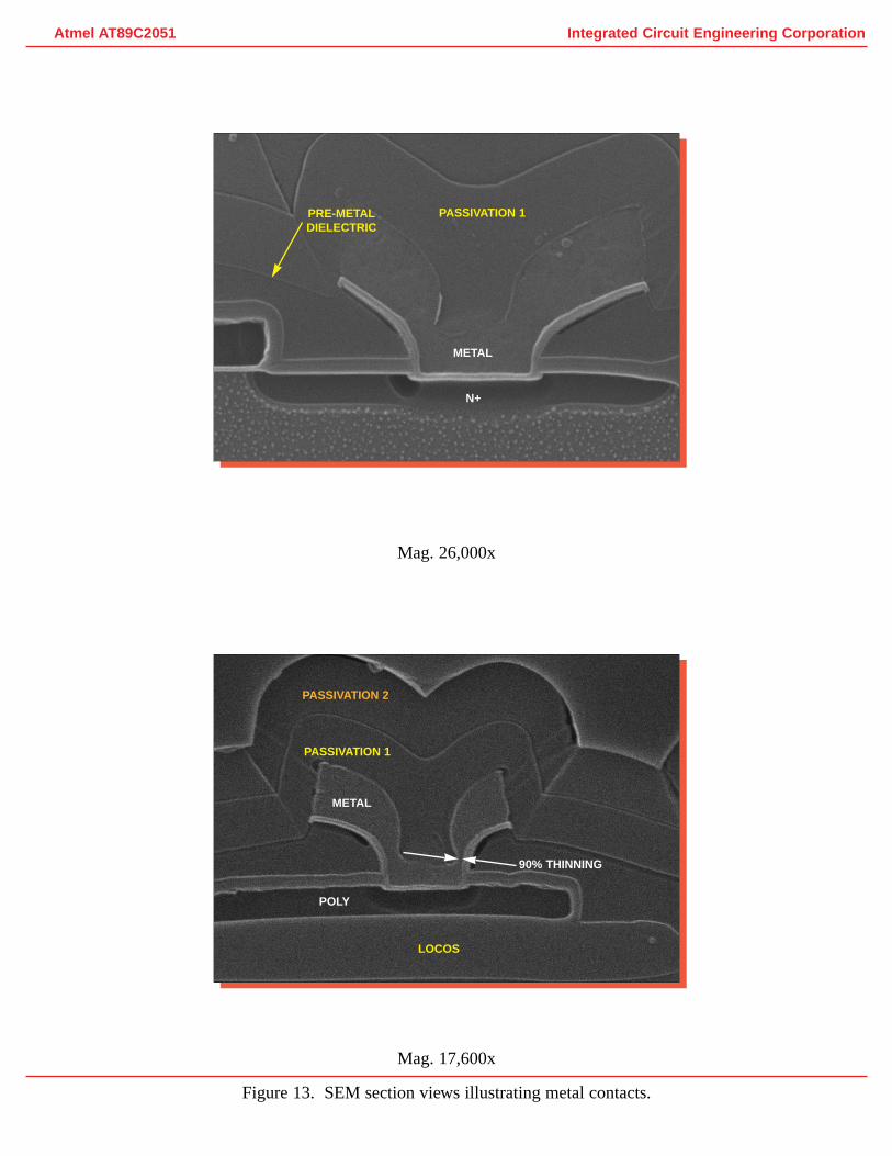
• Metal 1 aluminum thinning up to 90 percent2 at some contact edges on the AT89C2051
(Figure 13).
Special Features: None.
Noteworthy Items:
• Both devices are of similar structure; however, there are distinct differences. The
Flash cell design is the same on both devices; however, the cell of the AT89S8252
is smaller. The AT89S8252 also has an EEPROM memory. Cell design is identical
and the only distinction between the Flash and the EEPROM memory appears to be
the method in which the cells are erased. The other significant difference is that the
AT89S8252 employs a second metal layer which is used sparsely, mainly to
connect circuit blocks.
1These items present possible quality or reliability concerns. They should be discussed with the manufacturer to determine their possible impact on the intended application.
2Seriousness depends on design margins.
- 2 -
TECHNOLOGY DESCRIPTION
Assembly (AT89C2051 device only unless indicated):
• 20-pin plastic Dual-In-line Package (DIP).
• 40-pin plastic Dual-In-line Package (DIP) AT89S8252.
• External leads plated with tin-lead (SnPb) and internally spot-plated with silver (Ag).
• A silver-epoxy die attach was employed on both die.
• Die coat was not employed on either die.
• Lead-locking provisions (holes) were present at all pins.
• Multiple wirebonds were used at Vcc and GND pins to provide extra current-
carrying capacity. A bonding wire was connected from ground to the paddle for
biasing purposes.
• Thermosonic wirebonding using 1.2 mil O.D. gold wire.
• Dicing was by sawing (full depth) on both die.
Die Process and Design
• Note: Process description is same on both devices except where noted.
• Fabrication process: CMOS process employing twin-wells, on a P-substrate.
• Final passivation: Two thick layers of silicon-dioxide.
- 3 -
TECHNOLOGY DESCRIPTION (continued)
• Metallization: Single level metallization was used on the AT89C2051 device. No
cap was used; however a titanium-nitride barrier was employed. The metal was
defined by a standard dry etch. Two levels of metallization were used on the
AT89S8252 device. Metal 2 employed a titanium-nitride barrier and metal 1
employed a titanium-nitride cap and barrier. Metal 2 was sparsely used and
appeared to mainly connect circuit blocks together.
• Interlevel dielectric (AT89S8252 device only): The dielectric consisted of two layers
of glass. The first layer appeared to have been subjected to an etchback.
• Pre-metal: A single layer of reflow glass over grown oxides. The glass appeared to
have been reflowed following the contact cuts.
• Polysilicon: Two layers of standard poly silicon were employed. Poly 2 was used to
form all gates on the die and word lines and program lines in the EEPROM arrays.
Poly 1 was used exclusively in the EEPROM arrays where it formed the floating
gates.
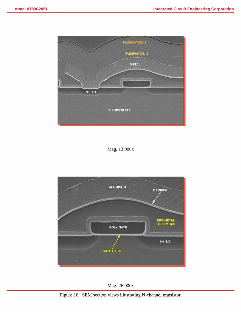
• Diffusions: Standard implanted N+ and P+ diffusions formed the sources/drains of
transistors. No sidewall spacers were present on the gates and no evidence of LDD
structures was found.
• Isolation: LOCOS, a step was noted in the local oxide at the well boundary
indicating a twin-well process was employed.
• Wells: Twin-wells in an P substrate.
• Fuses: No fuses were employed on this device.
• Buried contacts: No buried contacts were used.
- 4 -
TECHNOLOGY DESCRIPTION (continued)
• SRAM: The memory cell consisted of a 6T SRAM design. Metal 1 formed the bit
lines and distributed Vcc and GND. Poly 2 formed the word lines, storage gates
and pull-up devices.
• EEPROM: The memory cell design consisted of a poly 2 word line and program
line and a poly 1 floating gate. Metal one formed the bit lines. Programming is
achieved through ultra-thin tunnel oxide windows. Interpoly dielectric consisted of
an ONO dielectric. Both of the devices AT89S8252 and AT89C2051 have the
same layout design for both EEPROM (AT89S8252 only) and Flash memory.
However, the cell size of the AT89S8252 was about half the size of the cell on the
AT89C2051. On the AT89S8252 both EEPROM and Flash had the same design
on the AT89S8252 device, but the way the cells are erased distinguishes the two
types.
• MROM: An MROM cell array was employed on both devices. The cell was
programmed by the metal 1 layer. No detailed analysis of this memory was
performed since structures are the same as the peripheral circuits.
- 5 -
ANALYSIS RESULTS I
Assembly: Figures 1 - 4
Questionable Items:1 None.
Special Features: None.
General Items:
• Overall package quality: Good. No significant defects were found on the external or
internal portions of the packages on both die. No voids or cracks were noted in the
plastic package on both die.
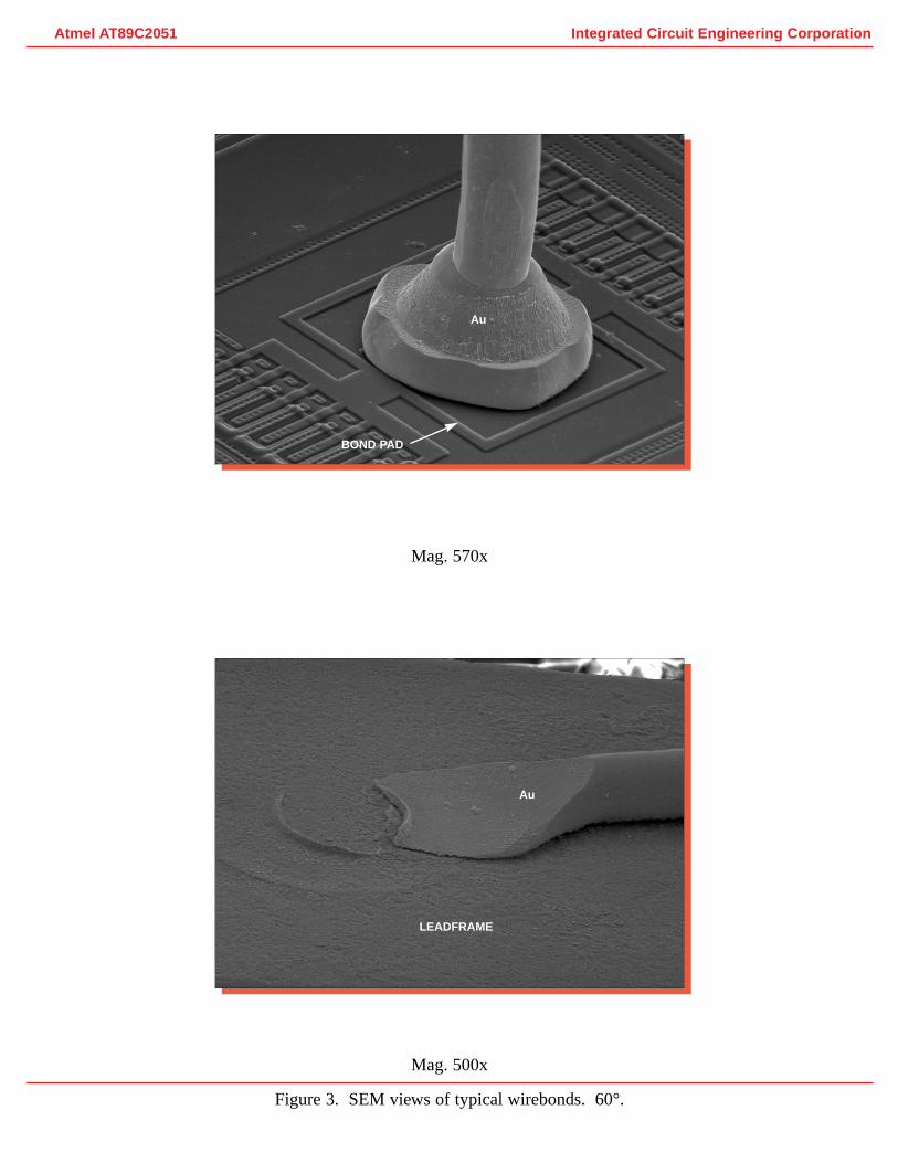
• Wirebonding: Thermosonic ball bond method using 1.2 mil gold wire. Bonds were
well formed and placement was good. All bond pull strengths were normal and no
bond lifts occurred (see page 11).
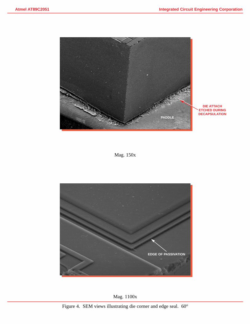
• Die attach: Silver-epoxy of normal quality. No problems were found.
• Die dicing: Die separation was by sawing (full depth) and showed normal quality
workmanship. No large chips or cracks were present at the die surface.
1These items present possible quality or reliability concerns. They should be discussed with the manufacturer to determine their possible impact on the intended application.
- 6 -
ANALYSIS RESULTS II
Die Process and Design: Figures 5 - 31
Questionable Items:1
• Metal 1 aluminum thinning up to 90 percent2 at some contact edges on the
AT89C2051 (Figure 13).
Special Features: None.
Noteworthy Items:
• Both devices are of similar structure; however, there are distinct differences. The
Flash cell design is the same on both devices; however, the cell of the AT89S8252
is smaller. The AT89S8252 also has an EEPROM memory. Cell design is identical
and the only distinction between the Flash and the EEPROM memory appears to be
the method in which the cells are erased. The other significant difference is that the
AT89S8252 employs a second metal which is used sparsely, mainly to connect
circuit blocks.
General Items:
• Fabrication process: CMOS process employing twin-wells in a P substrate. All P-
channel devices were formed in N-wells. All N-channel devices were formed in P-
wells. No epi was employed on these devices.
• Design implementation: Die layout was clean. Alignment was good at all levels.
1These items present possible quality or reliability concerns. They should be discussed with the manufacturer to determine their possible impact on the intended application.
2Seriousness depends on design margins.
- 7 -
ANALYSIS RESULTS II (continued)
• Surface defects: No contamination, processing defects or tool marks were found.
• Final passivation: Two thick layers of silicon-dioxide.
• Metallization: A single level metallization was used on the AT89C2051 device. No
cap was used; however a titanium-nitride barrier was employed. Two levels of
metallization were used on the AT89S8252 device. Metal 2 employed a titanium-
nitride barrier and metal 1 employed a titanium-nitride cap and barrier. Metal 2 was
used mainly to connect circuit blocks together.
• Metal patterning: The metal layers were defined by standard dry etch. Metal
completely surrounded all contacts. Standard contacts were employed (no plugs).
• Metal defects: No notching or voiding was found. No silicon nodules were
observed following removal of the aluminum layers.
• Metal step coverage: Metal 1 aluminum thinning was up to 90 percent thinning
(Figure 13) at some contacts. The amount of thinning is excessive a manufacturer’s
design specifications should be verified (AT89C2051 only).
• Contacts: Contacts were overetched slightly into the substrate and polysilicon;
however, no problems are foreseen.
• Interlevel dielectric (AT89S8252 device only): The dielectric consisted of two layers
of glass. The first layer appeared to have been subjected to an etchback. No
problems were noted.
• Pre-metal: A single layer of reflow glass over grown oxides. The glass was
reflowed following the contact cuts. No problems were found.
- 8 -
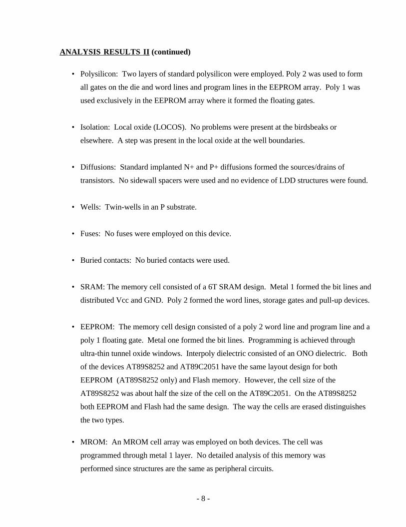
ANALYSIS RESULTS II (continued)
• Polysilicon: Two layers of standard polysilicon were employed. Poly 2 was used to form
all gates on the die and word lines and program lines in the EEPROM array. Poly 1 was
used exclusively in the EEPROM array where it formed the floating gates.
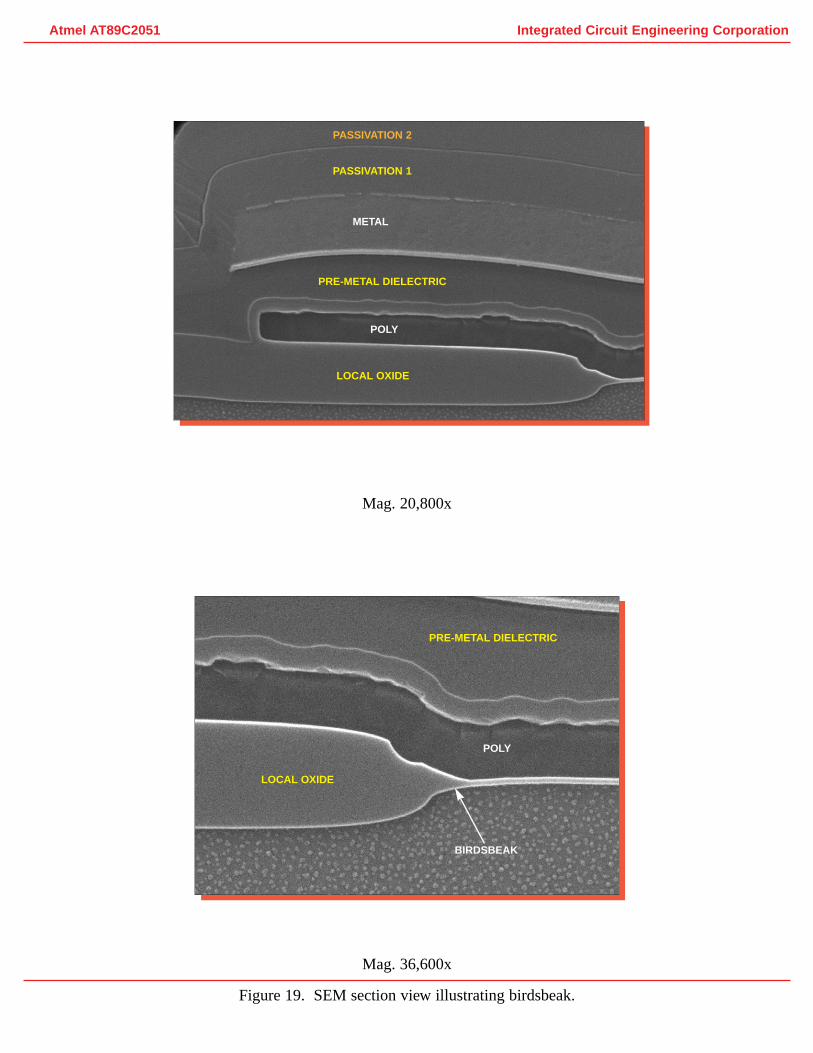
• Isolation: Local oxide (LOCOS). No problems were present at the birdsbeaks or
elsewhere. A step was present in the local oxide at the well boundaries.
• Diffusions: Standard implanted N+ and P+ diffusions formed the sources/drains of
transistors. No sidewall spacers were used and no evidence of LDD structures were found.
• Wells: Twin-wells in an P substrate.
• Fuses: No fuses were employed on this device.
• Buried contacts: No buried contacts were used.
• SRAM: The memory cell consisted of a 6T SRAM design. Metal 1 formed the bit lines and
distributed Vcc and GND. Poly 2 formed the word lines, storage gates and pull-up devices.
• EEPROM: The memory cell design consisted of a poly 2 word line and program line and a
poly 1 floating gate. Metal one formed the bit lines. Programming is achieved through
ultra-thin tunnel oxide windows. Interpoly dielectric consisted of an ONO dielectric. Both
of the devices AT89S8252 and AT89C2051 have the same layout design for both
EEPROM (AT89S8252 only) and Flash memory. However, the cell size of the
AT89S8252 was about half the size of the cell on the AT89C2051. On the AT89S8252
both EEPROM and Flash had the same design. The way the cells are erased distinguishes
the two types.
• MROM: An MROM cell array was employed on both devices. The cell was
programmed through metal 1 layer. No detailed analysis of this memory was
performed since structures are the same as peripheral circuits.

- 9 -
PROCEDURE
The devices were subjected to the following analysis procedures:
External inspection
Decapsulation
Optical inspection
Wirepull test
SEM of passivation and assembly features
Passivation removal and inspect metal
Aluminum removal
Delayer to poly and inspect
Die sectioning (90° for SEM)*
Measure horizontal dimensions
Measure vertical dimensions
Die material analysis
*Delineation of cross-sections is by silicon etch unless otherwise indicated.
- 10 -
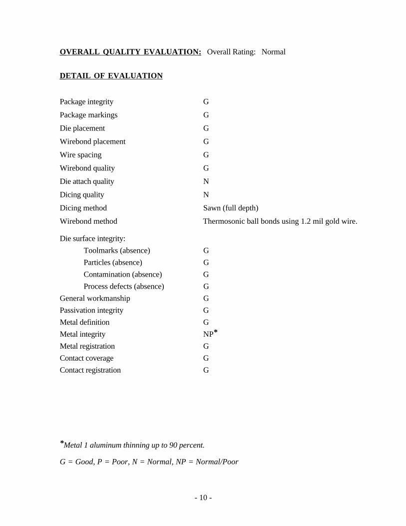
OVERALL QUALITY EVALUATION: Overall Rating: Normal
DETAIL OF EVALUATION
Package integrity G
Package markings G
Die placement G
Wirebond placement G
Wire spacing G
Wirebond quality G
Die attach quality N
Dicing quality N
Dicing method Sawn (full depth)
Wirebond method Thermosonic ball bonds using 1.2 mil gold wire.
Die surface integrity:
Toolmarks (absence) G
Particles (absence) G
Contamination (absence) G
Process defects (absence) G
General workmanship G
Passivation integrity G
Metal definition G
Metal integrity NP*
Metal registration G
Contact coverage G
Contact registration G
*Metal 1 aluminum thinning up to 90 percent.
G = Good, P = Poor, N = Normal, NP = Normal/Poor
- 11 -
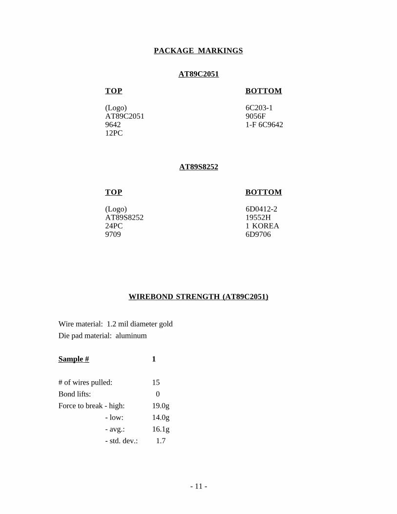
PACKAGE MARKINGS
AT89C2051
TOP BOTTOM
(Logo) 6C203-1AT89C2051 9056F9642 1-F 6C964212PC
AT89S8252
TOP BOTTOM
(Logo) 6D0412-2AT89S8252 19552H24PC 1 KOREA9709 6D9706
WIREBOND STRENGTH (AT89C2051)
Wire material: 1.2 mil diameter gold
Die pad material: aluminum
Sample # 1
# of wires pulled: 15
Bond lifts: 0
Force to break - high: 19.0g
- low: 14.0g
- avg.: 16.1g
- std. dev.: 1.7

- 12 -
DIE MATERIALS
Passivation: Two layers of silicon-dioxide.
Metal 2 (AT89S8252 device only): Aluminum with a titanium-nitridebarrier.
Metal 1: Aluminum with a titanium-nitridebarrier. Metal 1 also employed atitanium-nitride cap on the AT89S8252device.
Interlevel dielectric (AT89S8252 device only): Two layers of silicon-dioxide.
Pre-metal dielectric: BPSG glass.
- 13 -
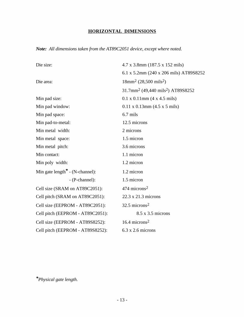
HORIZONTAL DIMENSIONS
Note: All dimensions taken from the AT89C2051 device, except where noted.
Die size: 4.7 x 3.8mm (187.5 x 152 mils)
6.1 x 5.2mm (240 x 206 mils) AT89S8252
Die area: 18mm2 (28,500 mils2)
31.7mm2 (49,440 mils2) AT89S8252
Min pad size: 0.1 x 0.11mm (4 x 4.5 mils)
Min pad window: 0.11 x 0.13mm (4.5 x 5 mils)
Min pad space: 6.7 mils
Min pad-to-metal: 12.5 microns
Min metal width: 2 microns
Min metal space: 1.5 micron
Min metal pitch: 3.6 microns
Min contact: 1.1 micron
Min poly width: 1.2 micron
Min gate length* - (N-channel): 1.2 micron
- (P-channel): 1.5 micron
Cell size (SRAM on AT89C2051): 474 microns2
Cell pitch (SRAM on AT89C2051): 22.3 x 21.3 microns
Cell size (EEPROM - AT89C2051): 32.5 microns2
Cell pitch (EEPROM - AT89C2051): 8.5 x 3.5 microns
Cell size (EEPROM - AT89S8252): 16.4 microns2
Cell pitch (EEPROM - AT89S8252): 6.3 x 2.6 microns
*Physical gate length.
- 14 -
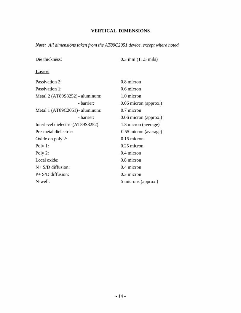
VERTICAL DIMENSIONS
Note: All dimensions taken from the AT89C2051 device, except where noted.
Die thickness: 0.3 mm (11.5 mils)
Layers
Passivation 2: 0.8 micron
Passivation 1: 0.6 micron
Metal 2 (AT89S8252) - aluminum: 1.0 micron
- barrier: 0.06 micron (approx.)
Metal 1 (AT89C2051)- aluminum: 0.7 micron
- barrier: 0.06 micron (approx.)
Interlevel dielectric (AT89S8252): 1.3 micron (average)
Pre-metal dielectric: 0.55 micron (average)
Oxide on poly 2: 0.15 micron
Poly 1: 0.25 micron
Poly 2: 0.4 micron
Local oxide: 0.8 micron
N+ S/D diffusion: 0.4 micron
P+ S/D diffusion: 0.3 micron
N-well: 5 microns (approx.)
INDEX TO FIGURES
AT89C2051
PACKAGE PHOTOS AND X-RAY Figures 1 - 2
PACKAGE ASSEMBLY Figures 3 - 4
DIE LAYOUT AND IDENTIFICATION Figures 5 - 7
PHYSICAL DIE STRUCTURES Figures 8 - 19
MEMORY CELL STRUCTURES Figures 20- 30
COLOR PROCESS DRAWING Figure 31
AT89S8252
PACKAGE PHOTOS Figure 32
DIE LAYOUT AND IDENTIFICATION Figures 33 - 34
PHYSICAL DIE STRUCTURES Figures 35 - 36
MEMORY CELL STRUCTURES Figures 37 - 42
- ii -
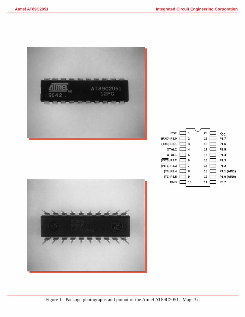
Integrated Circuit Engineering CorporationAtmel AT89C2051
Figure 1. Package photographs and pinout of the Atmel AT89C2051. Mag. 3x.
RST
(RXD) P3.0
(TXD) P3.1
XTAL2
XTAL1
(INT0) P3.2
(INT1) P3.3
(T0) P3.4
(T1) P3.5
GND
V
P1.7
P1.6
P1.5
P1.4
P1.3
P1.2
P1.1 (AIN1)
P1.0 (AIN0)
P3.7
1
2
3
4
5
6
7
8
9
10
20
19
18
17
16
15
14
13
12
11
CC
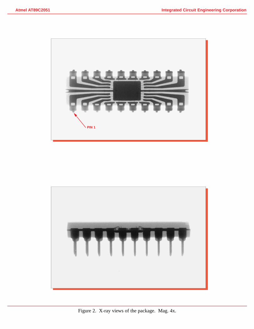
Figure 2. X-ray views of the package. Mag. 4x.
Integrated Circuit Engineering CorporationAtmel AT89C2051
PIN 1
Mag. 500x
Mag. 570x
Figure 3. SEM views of typical wirebonds. 60°.
Integrated Circuit Engineering CorporationAtmel AT89C2051
Au
Au
BOND PAD
LEADFRAME
Mag. 1100x
Mag. 150x
Figure 4. SEM views illustrating die corner and edge seal. 60°
Integrated Circuit Engineering CorporationAtmel AT89C2051
EDGE OF PASSIVATION
PADDLE
DIE ATTACHETCHED DURINGDECAPSULATION
Integrated Circuit Engineering CorporationAtmel AT89C2051
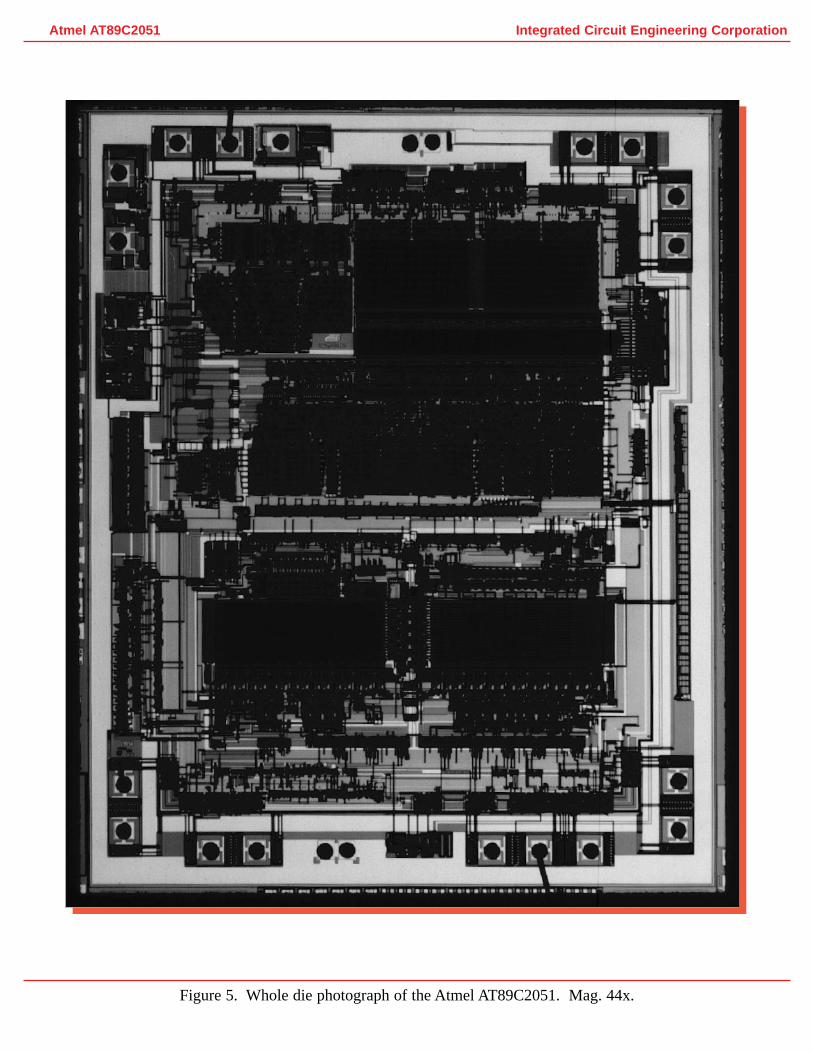
Figure 5. Whole die photograph of the Atmel AT89C2051. Mag. 44x.

Figure 6. Optical views illustrating markings on the die surface. Mag. 320x.
Integrated Circuit Engineering CorporationAtmel AT89C2051
Figu
re 7
. O
ptic
al v
iews
of d
ie c
orner
s.
Mag
. 10
0x.
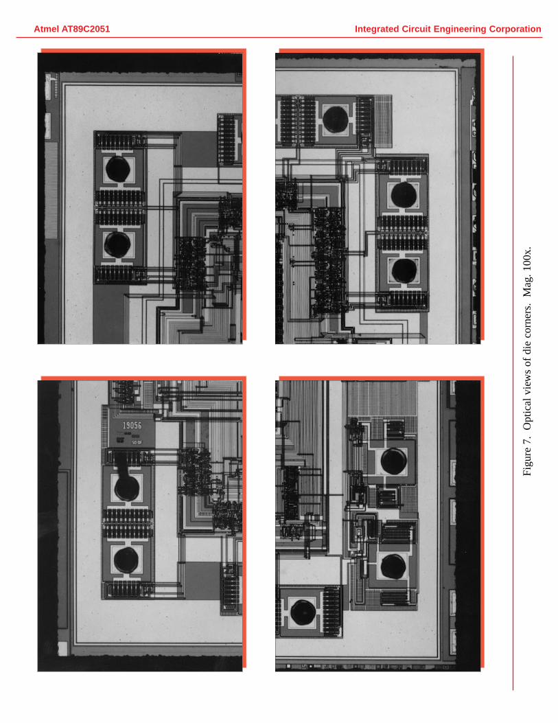
Integrated Circuit Engineering CorporationAtmel AT89C2051
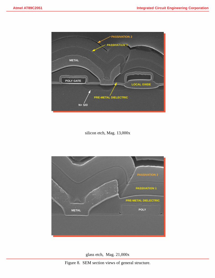
glass etch, Mag. 21,000x
silicon etch, Mag. 13,000x
Figure 8. SEM section views of general structure.
Integrated Circuit Engineering CorporationAtmel AT89C2051
PASSIVATION 2
PASSIVATION 1
METAL
LOCAL OXIDE
PRE-METAL DIELECTRIC
N+ S/D
PASSIVATION 2
PASSIVATION 1
METAL
PRE-METAL DIELECTRIC
POLY GATE
POLY
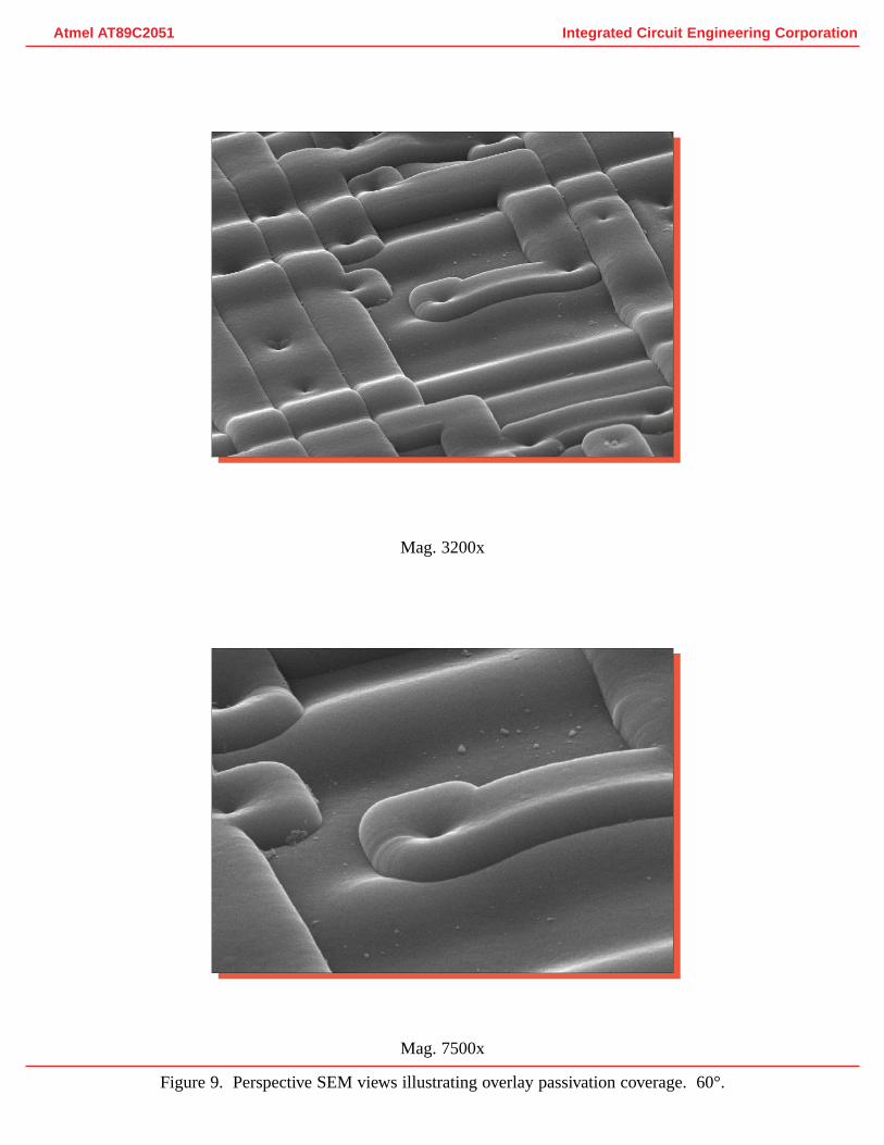
Mag. 7500x
Mag. 3200x
Figure 9. Perspective SEM views illustrating overlay passivation coverage. 60°.
Integrated Circuit Engineering CorporationAtmel AT89C2051
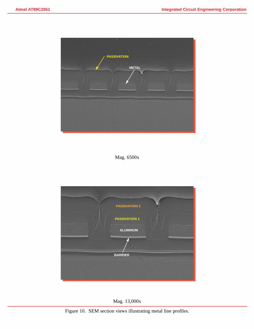
Mag. 13,000x
Mag. 6500x
Figure 10. SEM section views illustrating metal line profiles.
Integrated Circuit Engineering CorporationAtmel AT89C2051
PASSIVATION
PASSIVATION 2
PASSIVATION 1
ALUMINUM
BARRIER
METAL
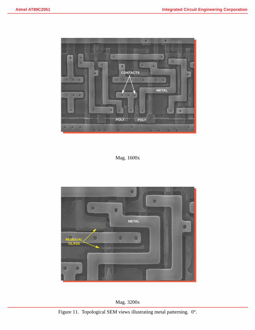
Mag. 3200x
Mag. 1600x
Figure 11. Topological SEM views illustrating metal patterning. 0°.
Integrated Circuit Engineering CorporationAtmel AT89C2051
METAL
POLYPOLY
METAL
RESIDUALGLASS
CONTACTS
Mag. 13,000x
Mag. 3700x
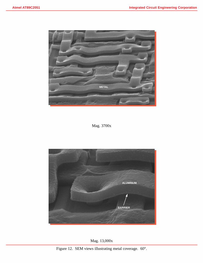
Figure 12. SEM views illustrating metal coverage. 60°.
Integrated Circuit Engineering CorporationAtmel AT89C2051
ALUMINUM
BARRIER
METAL
Mag. 17,600x
Mag. 26,000x
Figure 13. SEM section views illustrating metal contacts.
Integrated Circuit Engineering CorporationAtmel AT89C2051
METAL
N+
POLY
LOCOS
METAL
PASSIVATION 2
PASSIVATION 1
90% THINNING
PASSIVATION 1PRE-METALDIELECTRIC
Mag. 4700x
Mag. 2400x
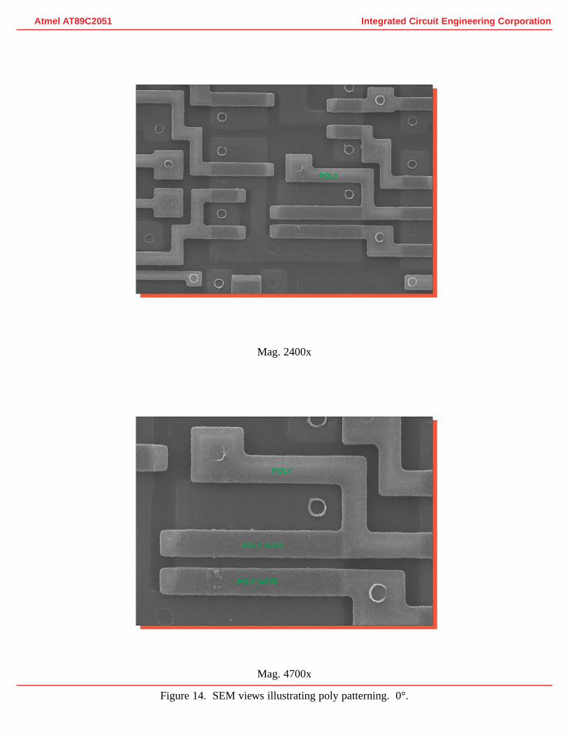
Figure 14. SEM views illustrating poly patterning. 0°.
Integrated Circuit Engineering CorporationAtmel AT89C2051
POLY
POLY
POLY GATE
POLY GATE

Mag. 4400x
Mag. 20,000x
Mag. 20,000x
Integrated Circuit Engineering CorporationAtmel AT89C2051
Figure 15. SEM views illustrating poly coverage. 60°.
P+
N+
POLY
POLY
POLY
Mag. 26,000x
Mag. 13,000x
Figure 16. SEM section views illustrating N-channel transistor.
Integrated Circuit Engineering CorporationAtmel AT89C2051
METAL
N+ S/D
PASSIVATION 1
P SUBSTRATE
POLY GATE
GATE OXIDE
N+ S/D
ALUMINUM
PRE-METALDIELECTRIC
BARRIER
PASSIVATION 2
Mag. 26,000x
Mag. 13,000x
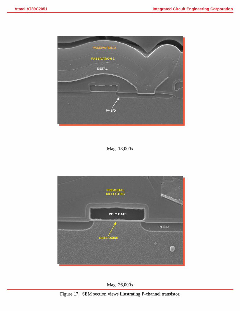
Figure 17. SEM section views illustrating P-channel transistor.
Integrated Circuit Engineering CorporationAtmel AT89C2051
METAL
P+ S/D
P+ S/D
PASSIVATION 1
PASSIVATION 2
POLY GATE
GATE OXIDE
PRE-METALDIELECTRIC
Mag. 13,000x
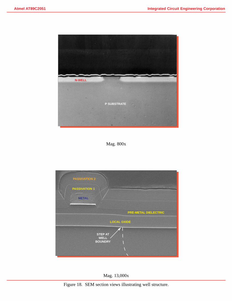
Mag. 800x
Figure 18. SEM section views illustrating well structure.
Integrated Circuit Engineering CorporationAtmel AT89C2051
P SUBSTRATE
N-WELL
METAL
PASSIVATION 1
PRE-METAL DIELECTRIC
LOCAL OXIDE
PASSIVATION 2
STEP ATWELL
BOUNDRY
Mag. 36,600x
Mag. 20,800x
Figure 19. SEM section view illustrating birdsbeak.
Integrated Circuit Engineering CorporationAtmel AT89C2051
METAL
PASSIVATION 1
PRE-METAL DIELECTRIC
LOCAL OXIDE
POLY
PRE-METAL DIELECTRIC
LOCAL OXIDE
BIRDSBEAK
POLY
PASSIVATION 2

unlayered
metal
Figure 20. Topological SEM views illustrating 6T SRAM array. Mag. 810x,0°.
Integrated Circuit Engineering CorporationAtmel AT89C2051
BIT LINES
POLY WORD LINES
unlayered
metal
Figure 21. Perspective SEM views illustrating 6T SRAM array. Mag. 1600x,60°.
Integrated Circuit Engineering CorporationAtmel AT89C2051
POLY WORD LINES
unlayered
metal
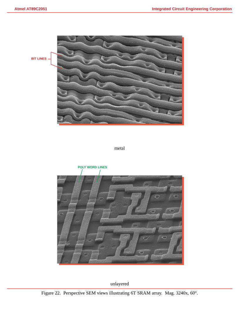
Figure 22. Perspective SEM views illustrating 6T SRAM array. Mag. 3240x,60°.
Integrated Circuit Engineering CorporationAtmel AT89C2051
BIT LINES
POLY WORD LINES

metal
unlayered
Integrated Circuit Engineering CorporationAtmel AT89C2051
4P
5N
6N
3N
2P
1NBIT BIT
WORD
Figure 23. Perspective SEM views illustrating 6T SRAM cell and schematic.Mag. 3200x,0°.
VCC
BIT
GND
VCC
GND
1
2
3
4
5
6
BIT
unlayered
metal
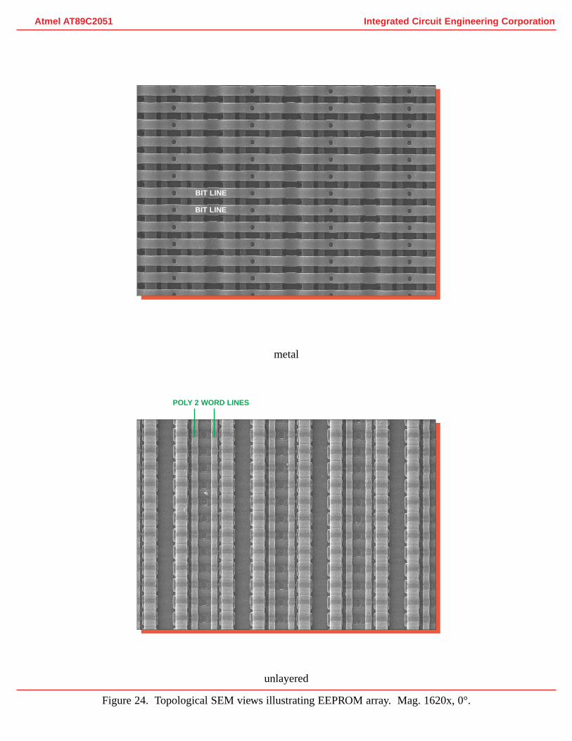
Figure 24. Topological SEM views illustrating EEPROM array. Mag. 1620x,0°.
Integrated Circuit Engineering CorporationAtmel AT89C2051
BIT LINE
BIT LINE
POLY 2 WORD LINES
unlayered
metal
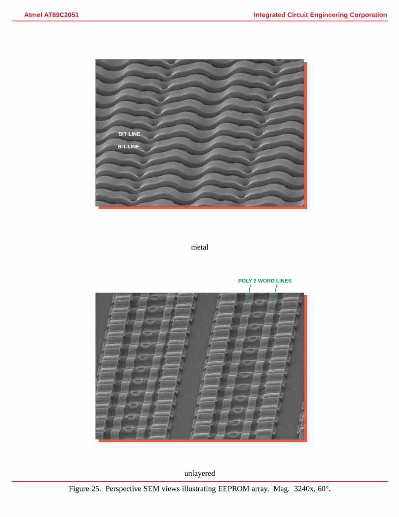
Figure 25. Perspective SEM views illustrating EEPROM array. Mag. 3240x,60°.
Integrated Circuit Engineering CorporationAtmel AT89C2051
BIT LINE
BIT LINE
POLY 2 WORD LINES
unlayered
metal
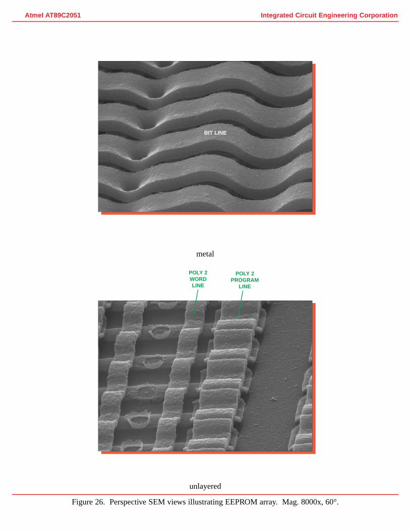
Figure 26. Perspective SEM views illustrating EEPROM array. Mag. 8000x,60°.
Integrated Circuit Engineering CorporationAtmel AT89C2051
BIT LINE
POLY 2WORDLINE
POLY 2PROGRAM
LINE
Mag. 20,000x
Mag. 13,000x
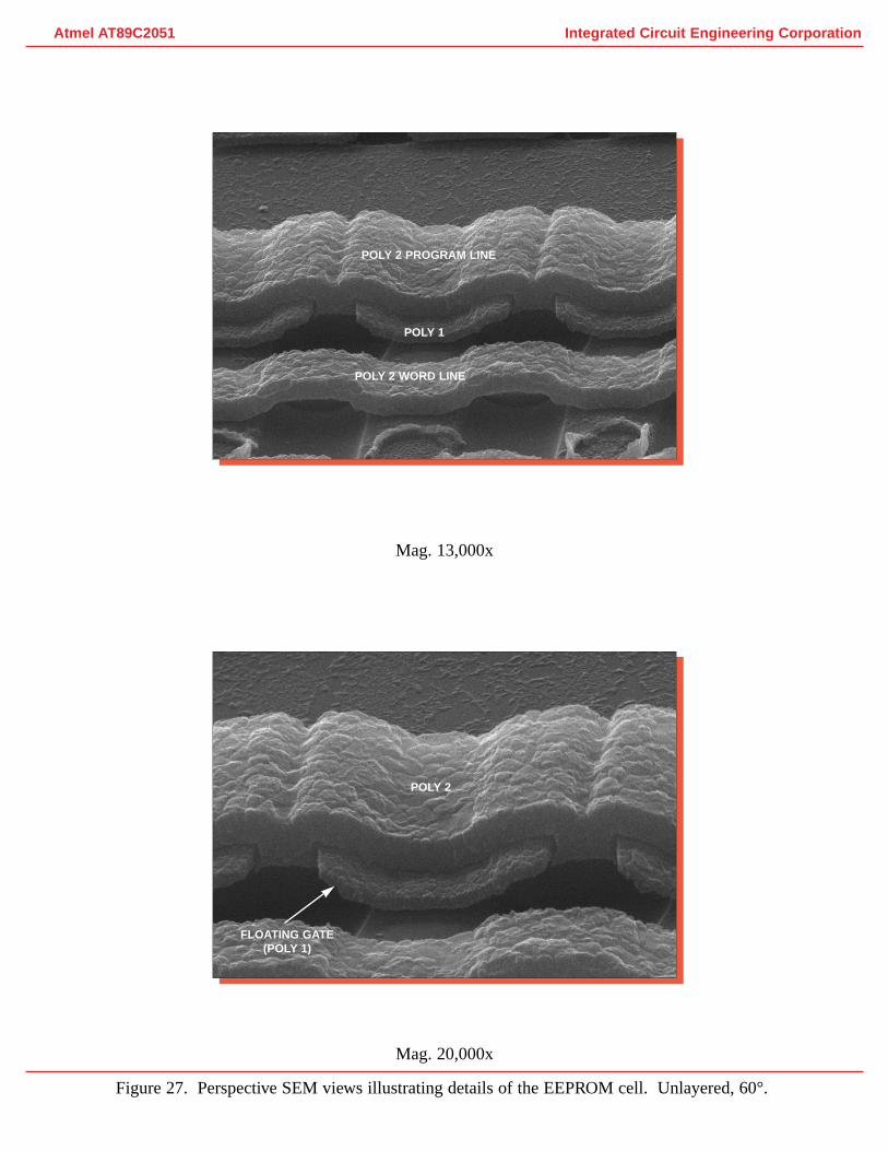
Figure 27. Perspective SEM views illustrating details of the EEPROM cell. Unlayered, 60°.
Integrated Circuit Engineering CorporationAtmel AT89C2051
FLOATING GATE(POLY 1)
POLY 2
POLY 2 WORD LINE
POLY 2 PROGRAM LINE
POLY 1
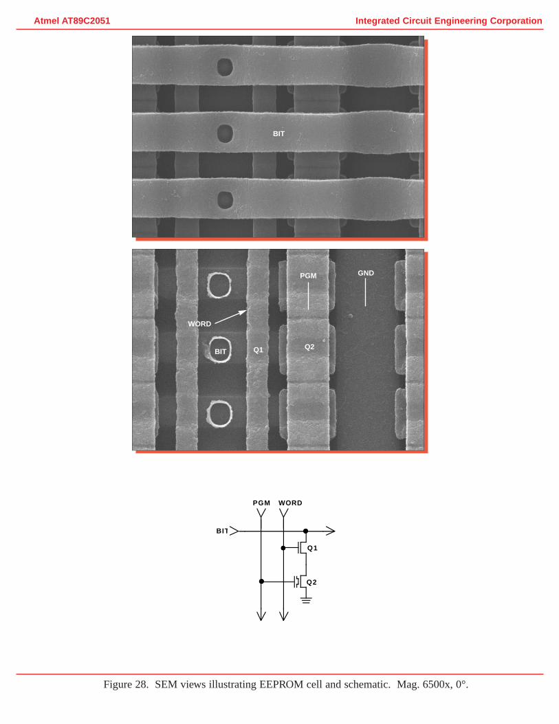
Integrated Circuit Engineering CorporationAtmel AT89C2051
PGM
BIT
WORD
Q1
Q2
Figure 28. SEM views illustrating EEPROM cell and schematic. Mag. 6500x,0°.
BIT Q1 Q2
PGM GND
BIT
WORD
Mag. 3240x
Mag. 13,000x
Mag. 26,000x
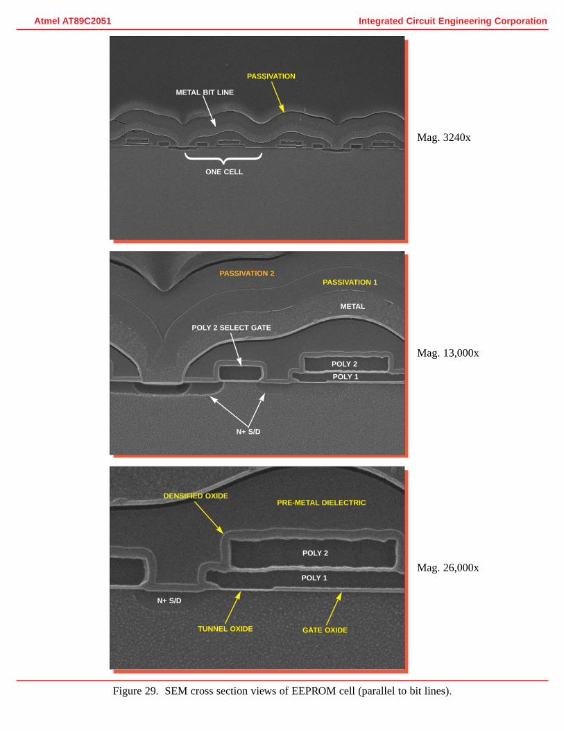
Integrated Circuit Engineering CorporationAtmel AT89C2051
Figure 29. SEM cross section views of EEPROM cell (parallel to bit lines).
PASSIVATION 2
POLY 2 SELECT GATE
N+ S/D
N+ S/D
METAL BIT LINE
ONE CELL
112233
PASSIVATION 1
PASSIVATION
METAL
POLY 2
POLY 1
POLY 2
POLY 1
GATE OXIDETUNNEL OXIDE
DENSIFIED OXIDEPRE-METAL DIELECTRIC
Mag. 13,000x
Mag. 6500x
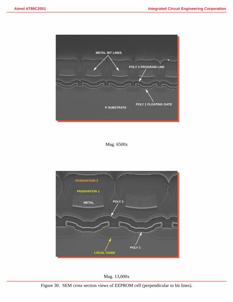
Figure 30. SEM cross section views of EEPROM cell (perpendicular to bit lines).
Integrated Circuit Engineering CorporationAtmel AT89C2051
P SUBSTRATEPOLY 1 FLOATING GATE
POLY 2 PROGRAM LINE
METAL BIT LINES
POLY 2
LOCAL OXIDE
METAL
POLY 1
PASSIVATION 2
PASSIVATION 1
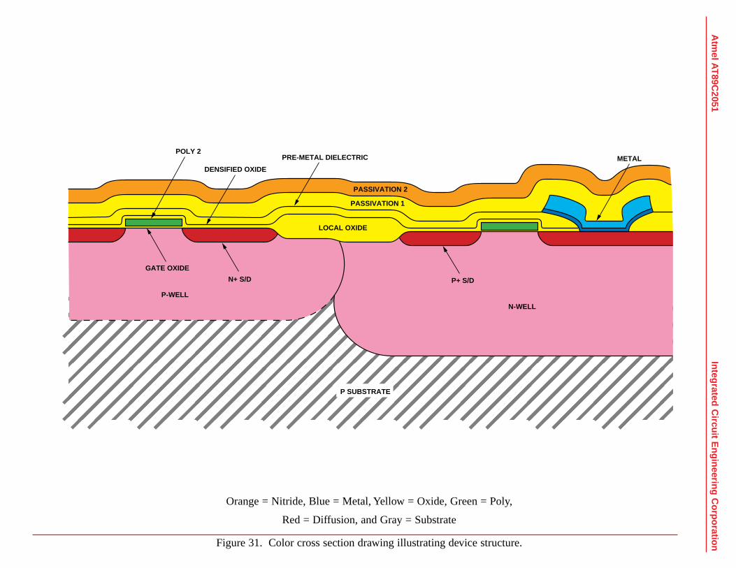
Figure 31. Color cross section drawing illustrating device structure.
Orange = Nitride, Blue = Metal,Yellow = Oxide, Green = Poly,
Red = Diffusion,and Gray = Substrate
Integrated Circuit E
ngineering Corporation
Atm
el AT
89C2051
����������������������������������������������������������������������������
METAL
PASSIVATION 1
PASSIVATION 2
LOCAL OXIDE
PRE-METAL DIELECTRICPOLY 2
DENSIFIED OXIDE
P+ S/D
N-WELL
P-WELL
N+ S/D
GATE OXIDE
P SUBSTRATE

Figure 32. Package photographs of the Atmel AT89S8252. Mag. 1.7x.
Integrated Circuit Engineering CorporationAtmel AT89S8252
Integrated Circuit Engineering CorporationAtmel AT89S8252
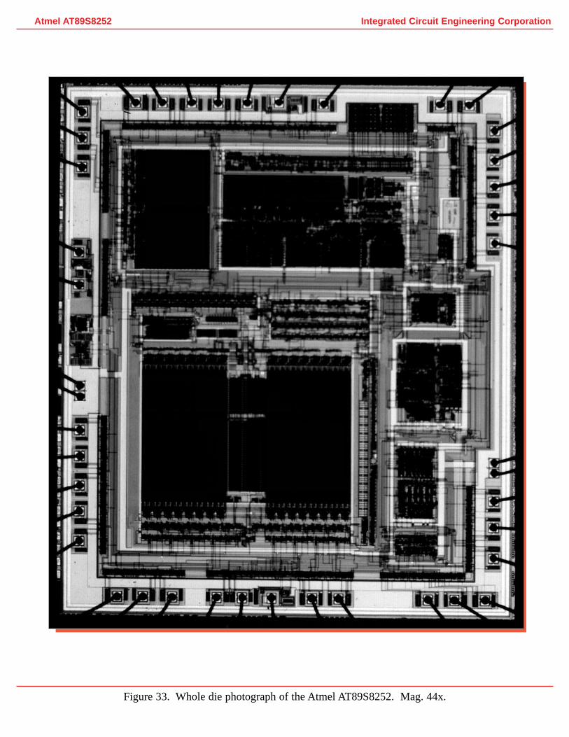
Figure 33. Whole die photograph of the Atmel AT89S8252. Mag. 44x.
Mag. 500x
Mag. 400x
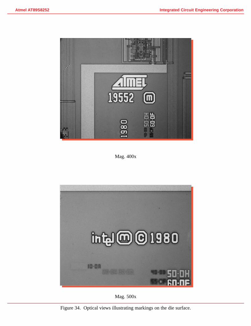
Figure 34. Optical views illustrating markings on the die surface.
Integrated Circuit Engineering CorporationAtmel AT89S8252
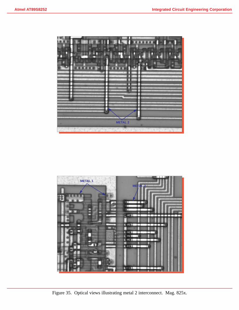
Figure 35. Optical views illustrating metal 2 interconnect. Mag. 825x.
Integrated Circuit Engineering CorporationAtmel AT89S8252
METAL 2
METAL 2
METAL 1
Mag. 10,000x
Mag. 13,000x
Mag. 15,000x
Integrated Circuit Engineering CorporationAtmel AT89S8252
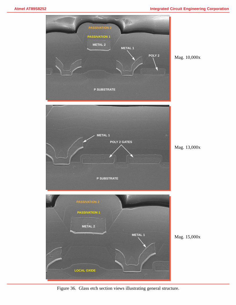
Figure 36. Glass etch section views illustrating general structure.
METAL 2
P SUBSTRATE
P SUBSTRATE
PASSIVATION 2
PASSIVATION 1
METAL 1
POLY 2
POLY 2 GATES
METAL 1
METAL 2
PASSIVATION 2
PASSIVATION 1
LOCAL OXIDE
METAL 1
Mag. 6500x
Mag. 1600x
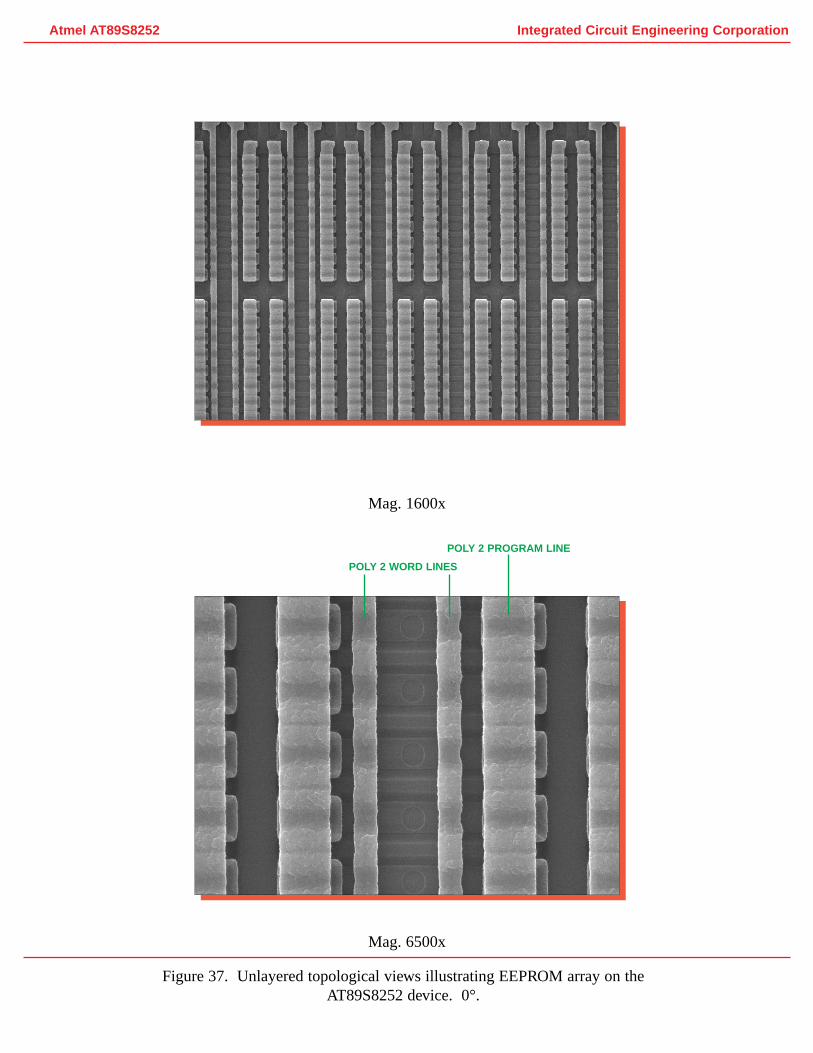
Figure 37. Unlayered topological views illustrating EEPROM array on theAT89S8252 device. 0°.
Integrated Circuit Engineering CorporationAtmel AT89S8252
POLY 2 WORD LINES
POLY 2 PROGRAM LINE
Mag. 3240x
Mag. 6500x
Mag. 13,000x
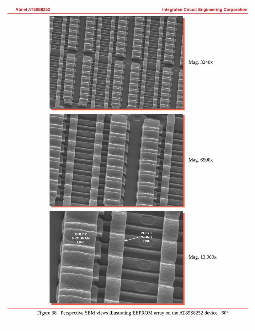
Integrated Circuit Engineering CorporationAtmel AT89S8252
Figure 38. Perspective SEM views illustrating EEPROM array on the AT89S8252 device. 60°.
POLY 2WORDLINE
POLY 2PROGRAM
LINE
Mag. 13,000x
Mag. 26,000x
Mag. 52,000x
Integrated Circuit Engineering CorporationAtmel AT89S8252
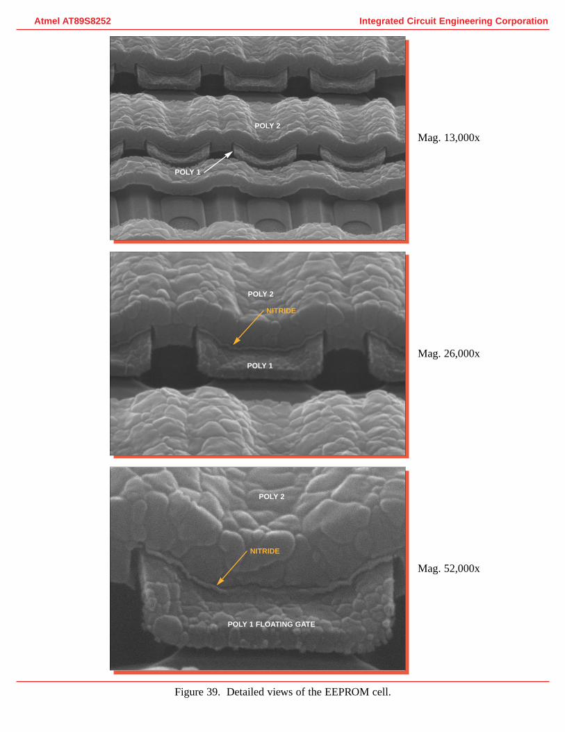
Figure 39. Detailed views of the EEPROM cell.
POLY 1
POLY 1
POLY 2
POLY 2
NITRIDE
POLY 1 FLOATING GATE
POLY 2
NITRIDE
Mag. 13,000x
Mag. 6500x
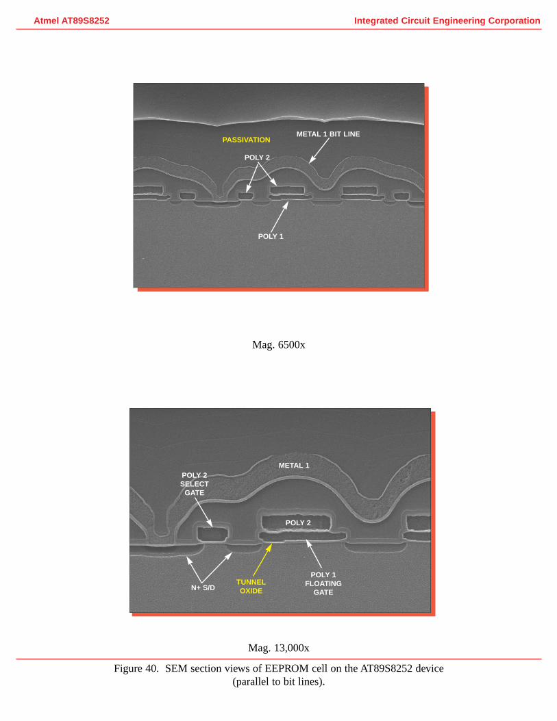
Figure 40. SEM section views of EEPROM cell on the AT89S8252 device(parallel to bit lines).
Integrated Circuit Engineering CorporationAtmel AT89S8252
METAL 1
N+ S/D
POLY 2
POLY 2SELECT
GATE
POLY 1FLOATING
GATETUNNELOXIDE
PASSIVATION
POLY 2
POLY 1
METAL 1 BIT LINE

Mag. 52,000x
Mag. 26,000x
Figure 41. Detailed SEM section views of EEPROM cell (parallel to bit lines).
Integrated Circuit Engineering CorporationAtmel AT89S8252
METAL
N+
POLY 2
POLY 1
TUNNEL OXIDE
POLY 2
POLY 1
TUNNEL OXIDE GATE OXIDE
DENSIFIED OXIDE
INTERPOLYDIELECTRIC
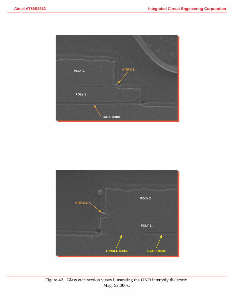
Figure 42. Glass etch section views illustrating the ONO interpoly dielectric. Mag. 52,000x.
Integrated Circuit Engineering CorporationAtmel AT89S8252
POLY 2
POLY 1
NITRIDE
GATE OXIDE
GATE OXIDETUNNEL OXIDE
POLY 2
POLY 1
NITRIDE