ATLAS pixel 3-D design using two tiers of electronics
21
June 6-11, 2010, Loch Lomond, Scotland June 6-11, 2010, Loch Lomond, Scotland P.Pangaud P.Pangaud ATLAS pixel 3-D design using two tiers of electronics P. Pangaud a , M. Barbero b , B. Chantepie a , J.C. Clémens a , R. Fei a , J. Fleury c , D. Fougeron a , M. Garcia-Sciveres c , S. Godiot a , T. Hemperek b , M. Karagounis b , H. Krueger b , A. Mekkaoui c , A. Rozanov a , N. Wermes b a Centre de Physique des Particules de Marseille, France b University of Bonn, Germany c Lawrence Berkeley National Laboratory, California, USA VERTEX 2010 19th International Workshop on Vertex Detectors
-
Upload
yasir-gallagher -
Category
Documents
-
view
16 -
download
1
description
VERTEX 2010 19th International Workshop on Vertex Detectors. ATLAS pixel 3-D design using two tiers of electronics. - PowerPoint PPT Presentation
Transcript of ATLAS pixel 3-D design using two tiers of electronics
June 6-11, 2010, Loch Lomond, ScotlandJune 6-11, 2010, Loch Lomond, ScotlandP.PangaudP.Pangaud
ATLAS pixel 3-D design using two tiers of
electronics
P. Pangaud a, M. Barbero b, B. Chantepie a, J.C. Clémens a, R. Fei a, J. Fleury c, D. Fougeron a, M. Garcia-Sciveres c, S. Godiot a , T. Hemperek b, M. Karagounis b,
H. Krueger b, A. Mekkaoui c, A. Rozanov a, N. Wermes b
a Centre de Physique des Particules de Marseille, France b University of Bonn, Germanyc Lawrence Berkeley National Laboratory, California, USA
VERTEX 2010 19th International Workshop on Vertex Detectors

22June 6-11, 2010, Loch Lomond, ScotlandJune 6-11, 2010, Loch Lomond, ScotlandP.PangaudP.Pangaud
Hybrid Pixels Detector for LHC/SLHC at CERN
LHC : Luminosity of 1034 cm-2.s-1
SLHC expected 10 times more !!!
Hybrid Pixels Detector of ATLAS/LHC Like a big camera with a 1.7 m2 area and 80
Million of Pixels with a snapshot every 25ns Hybrid Pixels Detector of ATLAS/SLHC
More luminosity, more pixels more ionizing particles, more … !!!

33June 6-11, 2010, Loch Lomond, ScotlandJune 6-11, 2010, Loch Lomond, ScotlandP.PangaudP.Pangaud
3-D motivations for ATLAS read-out chip upgrades Improve spatial resolution Deal with an increasing counting rate
Decrease pixel size
• 50
μm
• 50
μm
FE-I3 , 250 nmFE-I3 , 250 nm
400 μm
250 μm
FE-I4 , FE-I4 , 130 nm130 nm
125 μm
• 50
μm FE-TC4 , FE-TC4 ,
130 nm130 nm
Technology shrinking Vertical stacking
3-D benefits : Pixel size reduction Functionalities splitting Technologies mixing
3D pixel road map (A.Rozanov, ATLAS-France Paris, June 22, 2009) :

44June 6-11, 2010, Loch Lomond, ScotlandJune 6-11, 2010, Loch Lomond, ScotlandP.PangaudP.Pangaud
Context of ATLAS 3-D beginning…
Objectives :
Design a 3-D pixel based on the FE-I_4 pixel by splitting its functionalities into two parts :
one for the analogue functions, one for the digital parts.
Context :
2009 : First MPW run for High Energy Physics organized by FNAL with a consortium of 15 institutes (France, Germany, Italy, Poland and United-States)
The proposed 3-D process combines : CHARTERED 130nm technology TEZZARON 3D technology
55June 6-11, 2010, Loch Lomond, ScotlandJune 6-11, 2010, Loch Lomond, ScotlandP.PangaudP.Pangaud
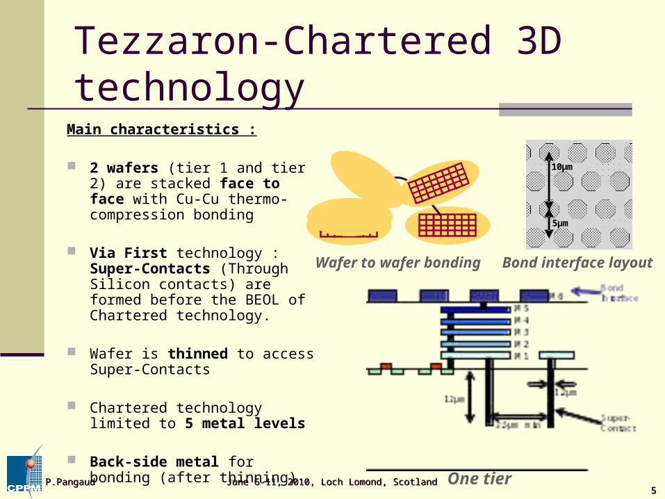
Tezzaron-Chartered 3D technology
Main characteristics :
2 wafers (tier 1 and tier 2) are stacked face to face with Cu-Cu thermo-compression bonding
Via First technology : Super-Contacts (Through Silicon contacts) are formed before the BEOL of Chartered technology.
Wafer is thinned to access Super-Contacts
Chartered technology limited to 5 metal levels
Back-side metal for bonding (after thinning) One tier
5µm
10µm
Bond interface layoutWafer to wafer bonding
66June 6-11, 2010, Loch Lomond, ScotlandJune 6-11, 2010, Loch Lomond, ScotlandP.PangaudP.Pangaud
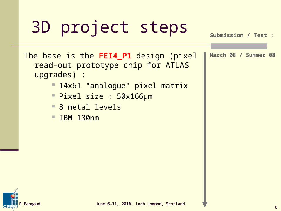
3D project steps
The base is the FEI4_P1 design (pixel read-out prototype chip for ATLAS upgrades) :
14x61 "analogue" pixel matrix Pixel size : 50x166µm 8 metal levels IBM 130nm
Submission / Test :
March 08 / Summer 08
77June 6-11, 2010, Loch Lomond, ScotlandJune 6-11, 2010, Loch Lomond, ScotlandP.PangaudP.Pangaud
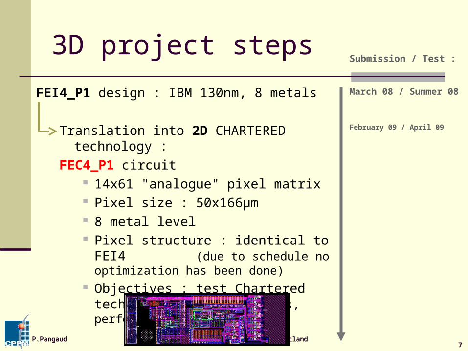
3D project steps
FEI4_P1 design : IBM 130nm, 8 metals
Translation into 2D CHARTERED technology :
FEC4_P1 circuit 14x61 "analogue" pixel matrix Pixel size : 50x166µm 8 metal level Pixel structure : identical to FEI4
(due to schedule no optimization has been done)
Objectives : test Chartered technology (functionalities, performances, radiation…)
Submission / Test :
March 08 / Summer 08
February 09 / April 09

88June 6-11, 2010, Loch Lomond, ScotlandJune 6-11, 2010, Loch Lomond, ScotlandP.PangaudP.Pangaud
FEC4_P1 test results
Even with no optimization for Chartered technology, main results are equivalent to IBM ones : Threshold min around 1100 e- Un-tuned threshold dispersion 200 e- Noise lower than 80 e-

99June 6-11, 2010, Loch Lomond, ScotlandJune 6-11, 2010, Loch Lomond, ScotlandP.PangaudP.Pangaud
FEC4_P1 test results
Irradiation performed at CERN/PS facility (24 GeV protons) up to 400 MRad Problem discovered after 160 MRad on latches ( output
tends to be blocked in "1" state) Difficult to work with the circuit by after Problem reproduced in simulation "corners" … but
Analog is still working even
with increased of noise :
250 e- (threshold dispersion
is meaningless)
1010June 6-11, 2010, Loch Lomond, ScotlandJune 6-11, 2010, Loch Lomond, ScotlandP.PangaudP.Pangaud
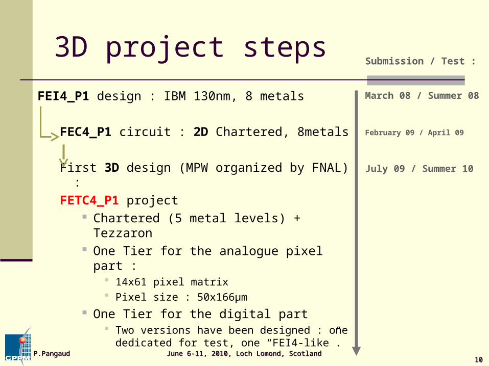
3D project steps
FEI4_P1 design : IBM 130nm, 8 metals
FEC4_P1 circuit : 2D Chartered, 8metals
First 3D design (MPW organized by FNAL) :
FETC4_P1 project Chartered (5 metal levels) + Tezzaron One Tier for the analogue pixel part :
14x61 pixel matrix Pixel size : 50x166µm
One Tier for the digital part Two versions have been designed : one
dedicated for test, one “FEI4-like”.
Submission / Test :
March 08 / Summer 08
February 09 / April 09
July 09 / Summer 10

1111June 6-11, 2010, Loch Lomond, ScotlandJune 6-11, 2010, Loch Lomond, ScotlandP.PangaudP.Pangaud
Chartered-Tezzaron MPW run
2 identical wafers are stacked Tier 1 and Tier 2 are in the same reticle.
4 sub-reticles for ATLAS/SLHC chips projects : FE_TC4_P1 + OmegaPix
C1, D1 = analog tier FE-TC4-AE + analog OmegaPix C2 = first version for digital tier (dedicated for test) : FE-TC4-DS D2 = second version for digital tier : FE-TC4-DC read-out structure “FEI4-like”+ digital OmegaPix
Chartered reticle :
26mm x 31mm
shared between all participants
1212June 6-11, 2010, Loch Lomond, ScotlandJune 6-11, 2010, Loch Lomond, ScotlandP.PangaudP.Pangaud
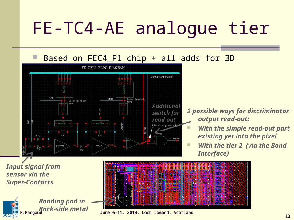
FE-TC4-AE analogue tier
Based on FEC4_P1 chip + all adds for 3D connection
2 possible ways for discriminator output read-out:
With the simple read-out part existing yet into the pixel
With the tier 2 (via the Bond Interface)
Input signal from sensor via the Super-Contacts
Additional switch for read-out
Bonding pad in Back-side metal

1313June 6-11, 2010, Loch Lomond, ScotlandJune 6-11, 2010, Loch Lomond, ScotlandP.PangaudP.Pangaud
FE-TC4-DS digital tier for test :parasitic coupling study between tiers
Analogue tier and digital tier are face to face (sensitive part facing digital part).
FE-TC4-DS : dedicated for parasitic coupling studies between the 2 tiers.
3 functions : Read the discriminator output Generate noise (digital
commutations) in front of 11 specific areas of the analogue pixel (preamplifier, feed-back, amplifier2, DAC…)
Test different shielding configurations.
Analogue pixel layout : 11 specific areas
M5 M4 M3 M2 M1
M6
SuperContact
M1 M2 M3 M4 M5
M6
SuperContact
Bond Interface
Tier 2
Tier 1 (thinned wafer)
Back Side Metal for bonding
ANALOGUE
DIGITAL
1414June 6-11, 2010, Loch Lomond, ScotlandJune 6-11, 2010, Loch Lomond, ScotlandP.PangaudP.Pangaud
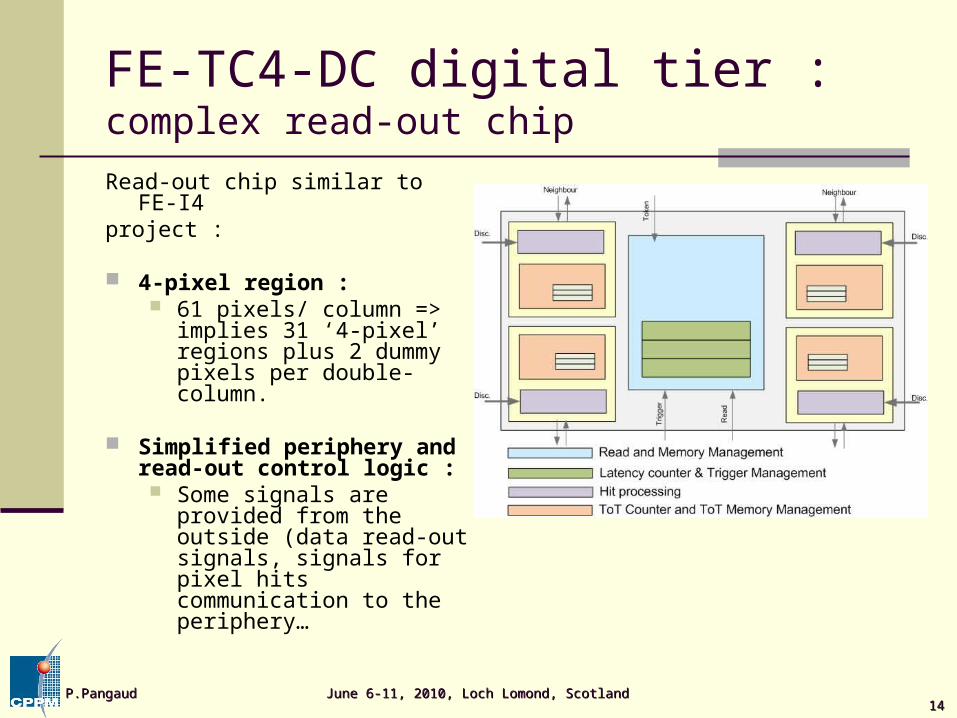
FE-TC4-DC digital tier :complex read-out chip
Read-out chip similar to FE-I4 project :
4-pixel region : 61 pixels/ column =>
implies 31 ‘4-pixel’ regions plus 2 dummy pixels per double-column.
Simplified periphery and read-out control logic : Some signals are provided
from the outside (data read-out signals, signals for pixel hits communication to the periphery…
1515June 6-11, 2010, Loch Lomond, ScotlandJune 6-11, 2010, Loch Lomond, ScotlandP.PangaudP.Pangaud
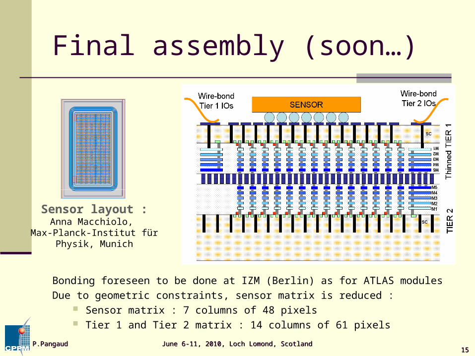
Final assembly (soon…)
Bonding foreseen to be done at IZM (Berlin) as for ATLAS modules
Due to geometric constraints, sensor matrix is reduced : Sensor matrix : 7 columns of 48 pixels Tier 1 and Tier 2 matrix : 14 columns of 61 pixels
Sensor layout :Anna Macchiolo,
Max-Planck-Institut für Physik, Munich

1616June 6-11, 2010, Loch Lomond, ScotlandJune 6-11, 2010, Loch Lomond, ScotlandP.PangaudP.Pangaud
FE-TC4-P1 test results
The submission of this first 3D MPW run organized by FNAL has encountered a lot of problems : Difficulties for the establishment of a good layout frame
reticle according to all requirements of Tezzaron and Chartered,
software development or adjustment to well considered all added 3D layers,
software limitations for checks, ... Long delay…
But tests are expected for this summer …

1717June 6-11, 2010, Loch Lomond, ScotlandJune 6-11, 2010, Loch Lomond, ScotlandP.PangaudP.Pangaud
3D project steps
FEI4_P1 design : IBM 130nm, 8 metals
FEC4_P1 circuit : 2D Chartered, 8metals
FETC4_P1 circuits : 3D first prototype
Second 2D prototype : FEC4_P2 circuit Chartered (8 metal levels) Based on FEC4_P1 circuit, plus :
Optimization of transistors New latches for irradiation tests New PadRing strategy and ground/substrate
separation
Submission / Test :
March 08 / Summer 08
February 09 / April 09
July 09 / Summer 10
November 09 / January 10

1919June 6-11, 2010, Loch Lomond, ScotlandJune 6-11, 2010, Loch Lomond, ScotlandP.PangaudP.Pangaud
3D project steps
FEI4_P1 design : IBM 130nm, 8 metals
FEC4_P1 circuit : 2D Chartered, 8 metals
FETC4_P1 circuits : 3D first prototype
FEC4_P2 circuit : 2D Chartered, 8 metals
FEC4_P3 : Third 2D Chartered prototype Chartered (8 metal levels but only 5 are used) Smaller pixel size : 50µm x 125µm Design of new sub-circuits and functionalities :
Current Reference Analogue multiplexor PLL Triple redundancy
Submission / Test :
March 08 / Summer 08
February 09 / April 09
July 09 / Summer 10
November 09 / January 10
September 10 / End of 10
2121June 6-11, 2010, Loch Lomond, ScotlandJune 6-11, 2010, Loch Lomond, ScotlandP.PangaudP.Pangaud
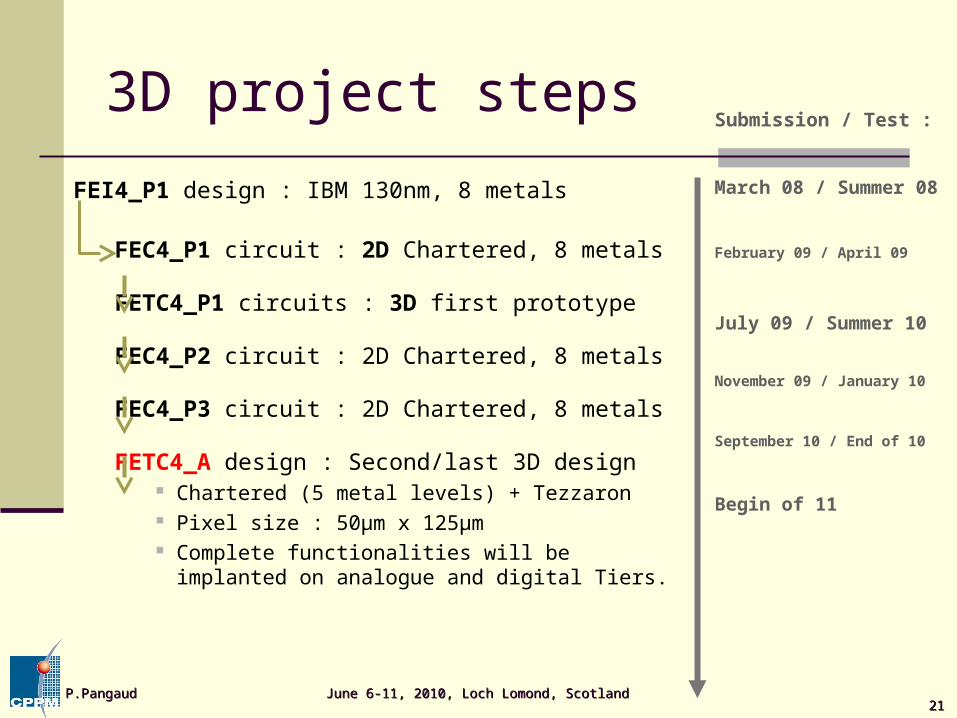
3D project steps
FEI4_P1 design : IBM 130nm, 8 metals
FEC4_P1 circuit : 2D Chartered, 8 metals
FETC4_P1 circuits : 3D first prototype
FEC4_P2 circuit : 2D Chartered, 8 metals
FEC4_P3 circuit : 2D Chartered, 8 metals
FETC4_A design : Second/last 3D design Chartered (5 metal levels) + Tezzaron Pixel size : 50µm x 125µm Complete functionalities will be implanted on
analogue and digital Tiers.
Submission / Test :
March 08 / Summer 08
February 09 / April 09
July 09 / Summer 10
November 09 / January 10
September 10 / End of 10
Begin of 11
2222June 6-11, 2010, Loch Lomond, ScotlandJune 6-11, 2010, Loch Lomond, ScotlandP.PangaudP.Pangaud
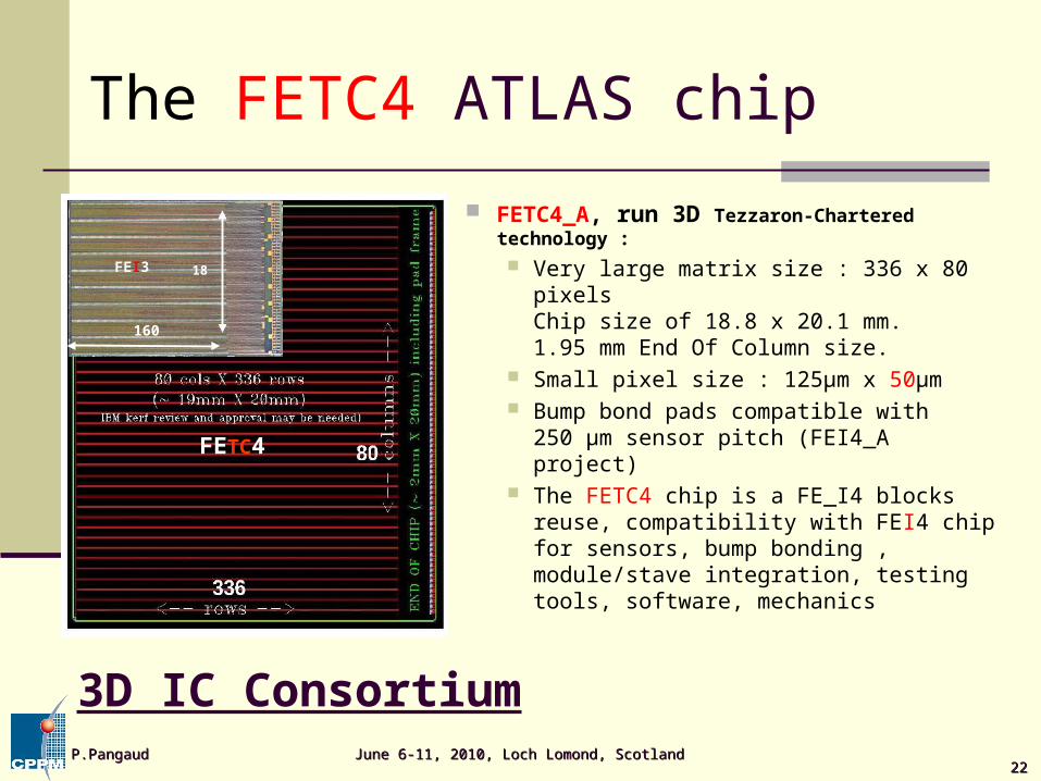
The FETC4 ATLAS chip
FETC4_A, run 3D Tezzaron-Chartered technology :
Very large matrix size : 336 x 80 pixels Chip size of 18.8 x 20.1 mm. 1.95 mm End Of Column size.
Small pixel size : 125µm x 50µm Bump bond pads compatible with
250 µm sensor pitch (FEI4_A project) The FETC4 chip is a FE_I4 blocks
reuse, compatibility with FEI4 chip for sensors, bump bonding , module/stave integration, testing tools, software, mechanics
160
18FEI3
FETC4
3D IC Consortium
2323June 6-11, 2010, Loch Lomond, ScotlandJune 6-11, 2010, Loch Lomond, ScotlandP.PangaudP.Pangaud
Conclusions and future plans
Benefits of 3D technology for hybrid pixel detectors : Pixel size reduction Technologies mixing More functionalities can be implemented in front of the analogue pixel Since 2 years
A 3D prototype, in Tezzaron-Chartered technology, was designed and submitted, as a test bench for this technology, in framework of ATLAS pixel upgrade for higher luminosities.
2D prototyping blocks, in Chartered technology only, were designed and tested to more quickly help the 3D approach.
Future Plans: Prototyping blocks in 2D Chartered in Summer (e.g. FEND, CREF,
CLKGEN, new LVDS…) placed into the FEC4_P3 Tests will be performed on FETC4_AEDS (DC) and on 3D test structures. FEC4_P2 chip (transistor optimization and few minor corrections) is under
test, and under radiation at CERN/PS. Start working to design a full scale FETC4_A