AT91SAM7L-STK Rev. B Starter Kit - Farnell element14 Rev. B Starter Kit User Guide 3-1...
40
6414A–ATARM–12-Sep-08 AT91SAM7L-STK Rev. B Starter Kit .................................................................................................................... User Guide
-
Upload
vuongtuong -
Category
Documents
-
view
215 -
download
2
Transcript of AT91SAM7L-STK Rev. B Starter Kit - Farnell element14 Rev. B Starter Kit User Guide 3-1...

AT91SAM7L-STK Rev. B Starter Kit....................................................................................................................
User Guide
6414A–ATARM–12-Sep-08

1-2 AT91SAM7L-STK Rev. B Starter Kit User Guide
6414A–ATARM–12-Sep-08

AT91SAM7L-STK
Table of Contents
Section 1Overview .................................................................................................................... 1-1
1.1 Introduction ........................................................................................................................ 1-1
Section 2Setting Up the AT91SAM7L-STK Board .................................................................... 2-1
2.1 Electrostatic Warning ......................................................................................................... 2-1
2.2 Requirements..................................................................................................................... 2-1
2.3 Power up the Board ........................................................................................................... 2-1
2.4 Debugging and Programming ............................................................................................ 2-1
Section 3Development Tools .................................................................................................... 3-1
3.1 Overview ............................................................................................................................ 3-1
3.2 Typical Development Connection ...................................................................................... 3-1
3.3 Integrated Development Environment ............................................................................... 3-1
3.4 SAM-ICE............................................................................................................................ 3-2
3.5 SAM-BA® ........................................................................................................................... 3-3
3.6 Sample Code and Technical Support ................................................................................ 3-4
Section 4Board Description....................................................................................................... 4-1
4.1 AT91SAM7L64/128 Microcontroller ................................................................................... 4-1
4.2 AT91SAM7L64/128 Block Diagram ................................................................................... 4-3
4.3 Overview ............................................................................................................................ 4-4
4.4 Processor........................................................................................................................... 4-4
4.5 Memory .............................................................................................................................. 4-5
4.6 Clock Circuitry.................................................................................................................... 4-5
4.7 Reset and Wake Up Circuitry............................................................................................. 4-6
4.8 Power Supply and Management........................................................................................ 4-6
4.9 DBGU................................................................................................................................. 4-9
4.10 JTAG/ICE........................................................................................................................... 4-9
4.11 Segment LCD .................................................................................................................. 4-10
4.12 User Buttons .................................................................................................................... 4-11
4.13 ZigBee.............................................................................................................................. 4-12
4.14 PIO Expansion ................................................................................................................. 4-13
4.15 User Grids........................................................................................................................ 4-13
Rev. B Starter Kit User Guide i
6414A–ATARM–12-Sep-08

Table of Contents (Continued)
ii
6414A–ATARM–12-Sep
Section 5Configuration .............................................................................................................. 5-1
5.1 PIO Usage ......................................................................................................................... 5-1
5.2 Jumpers ............................................................................................................................. 5-5
5.3 Test Points ......................................................................................................................... 5-5
5.4 Solder Drops ...................................................................................................................... 5-6
Section 6Schematics................................................................................................................. 6-1
Section 7Revision History ......................................................................................................... 7-1
AT91SAM7L-STK Rev. B Starter Kit User Guide
-08

Section 1
Overview
1.1 Introduction
Thank you for your purchase of the AT91SAM7L-STK starter kit. The AT91SAM7L-STK is a simplestarter kit and development system for the ARM® Thumb®-based AT91SAM7L series Flash Microcon-troller from Atmel Corporation. It is designed to give designers a quick start to evaluate the performanceand functionality of the AT91SAM7L series microcontroller and to develop code on it for prototyping andtesting of new designs.
This user guide is intended to familiarize users with the kit hardware and as an aid to develop their ownapplications.
AT91SAM7L-STK Rev. B Starter Kit User Guide 1-1
6414A–ATARM–12-Sep-08

Overview
1.1.1 Deliverables
Please unpack and inspect the AT91SAM7L-STK carefully and you will find the following items.
Board
– An AT91SAM7L-STK Board
Power Supply
– 2 AAA Batteries
Cable
– None
CD ROM
– SAM7L-STK CD ROM
Figure 1-1. Unpacked Kit
1-2 AT91SAM7L-STK Rev. B Starter Kit User Guide
6414A–ATARM–12-Sep-08

Overview
1.1.2 Starter Kit Features
RS232 Interface to PC for SAM-BA® Programming and Debugging
20-pin ICE Interface to SAM-ICE™ for Programming and Debugging
Battery Socket for 2 AAA Size Batteries 3.0V Power Supply
ZigBee® Interface for Atmel AT86RF230 Adaptor
Segment LCD (10 commons by 40 segments) for Display
5 Push Buttons for User’s Input
User’s Grid and PIO Extension Interface for Prototyping
Figure 1-2. Topview
The AT91SAM7L-STK is supported by SAM-BA version 2.7 or higher through DBGU or ICE interface forprogramming and debugging of the AT91SAM7L series Microcontroller. Also it is supported by manyother third-party software such as: IAR, GNU and Keil™, etc through ICE interface.
AT91SAM7L-STK Rev. B Starter Kit User Guide 1-3
6414A–ATARM–12-Sep-08

Overview
1.1.3 Board Specification
Table 1-1. AT91SAM7L-STK Specification
Characteristic Specification
Clock Speed Up to 36 MHz
Ports RS232
Board Supply Voltage 1.8 to 3.6V DC
Board Supply Current 18 mA typical (fully active, CPU at 36MHz)
TemperatureOperatingStorage
-10° to +50° C-40° to +85° C
Relative Humidity 0 to 90%
Dimensions 94 x 84 x 32 (L x W x H mm)
RoHS Compliant
1-4 AT91SAM7L-STK Rev. B Starter Kit User Guide
6414A–ATARM–12-Sep-08

Section 2
Setting Up the AT91SAM7L-STK Board
2.1 Electrostatic Warning
The AT91SAM7L-STK evaluation board is shipped in protective anti-static packaging. The board mustnot be subjected to high electrostatic potentials. A grounding strap or similar protective device should beworn when handling the board. Avoid touching the component or any other metallic element.
2.2 Requirements
In order to set up the AT91SAM7L-STK evaluation board, the following items are needed:
The AT91SAM7L-STK evaluation board itself.
2 AAA batteries
2.3 Power up the Board
The AT91SAM7L-STK is shipped with an AT91SAM7L128 microcontroller mounted on board. Thedefault jumper settings will allow the microcontroller to execute from the clock source and battery supplyon the board. The microcontroller is programmed with demonstration software in its embedded Flash.Follow below steps to make it work.
Put the 2 batteries into the battery holder, the board will go into power off mode directly.
Push WAKE UP button under the segment LCD, the demo software will start scrolling a welcome message on the segment LCD.
Push the RESET button, the board will go into power off mode again.
2.4 Debugging and Programming
The AT91SAM7L-STK is able to interface with SAM-BA® (v2.7 or higher) Boot Assistant software forSAM devices, and other third-party software. There is one RS232 port (DBGU) and one 20-pin ICE porton the AT91SAM7L-STK for such debugging and programming purpose. There is more detailed informa-tion about the development tools in Section 3, “Development Tools”.
2.4.0.1 ICE Interface
The SAM-ICE emulator needs to be connected between the AT91SAM7L-STK ICE port (J7) and the PCUSB port. You will also need to download the J-Link drivers for ARM from www.segger.com. Install thebatteries, push the WAKE UP button, and then you can run PC software, such as SAM-BA, for settingand programming the device, IAR or Keil to debug your code. For detailed information, please refer tothe SAM-BA user manual or that of the third-party software.
AT91SAM7L-STK Rev. B Starter Kit User Guide 2-1
6414A–ATARM–12-Sep-08

Setting Up the AT91SAM7L-STK Board
2.4.0.2 DBGU Interface
AT91SAM7L series Flash Microcontroller is able to boot from internal ROM or internal Flash memorythrough a general purpose NVM (GPNVM1) bit. When this bit is cleared, the MCU will boot from internalROM to enable the SAM-BA connection through DBUG.
Connect AT91SAM7L-STK DBGU port (J4) to PC COM port through an RS232 cable. Then you can runthe SAM-BA from the PC to program the internal Flash of the MCU as well as the GPNVM1 bit.
2-2 AT91SAM7L-STK Rev. B Starter Kit User Guide
6414A–ATARM–12-Sep-08

Section 3
Development Tools
3.1 Overview
This section offers a brief introduction to the hardware and software development tools required to testand develop custom applications on the AT91SAM7L-STK. Some development tools are needed as wellfor programming and debugging purposes. Refer to the user manuals of these tools for moreinformation.
3.2 Typical Development Connection
An RS232 serial cable is needed for DBGU SAM-BA communication. And a SAM-ICE interface isneeded for ICE debugging and programming.
Figure 3-1. Hardware Connection for Development
3.3 Integrated Development Environment
There are many development solutions in the ARM world today, commercial or non-commercial. Gener-ally speaking, commercial packages integrate all the tools required for embedded development and arewell-supported, such as IAR® Embedded Workbench and ARM® RealView®. Contact the tool supplier formore information.
Open-source solutions such as GNU tool chain are available as well. For a step-by-step guide for settingup a working GNU-based environment targeted at Atmel’s AT91SAM microcontroller family, refer toAtmel’s application note “GNU-Based Software Development on AT91SAM Microcontrollers”.
Serial Cross
DBGU
AT
91
SA
M7
L-S
TK
ICE
SAM-ICE
PC
AT91SAM7L-STK Rev. B Starter Kit User Guide 3-1
6414A–ATARM–12-Sep-08

Development Tools
3.4 SAM-ICE
SAM-ICE is a JTAG emulator designed for all Atmel AT91SAM ARM7™/ARM9™ cores. DLL files to sup-port SAM-ICE are available on the J-link ARM sub areas at www.segger.com. The J-Link softwarepackage is delivered as a ZIP file containing the setup program. After installation, SAM-ICE can be usedin debugging.
SAM-ICE Features:
Any Atmel AT91SAM ARM7/ARM9 core supported, including Thumb mode.
J-Link compatible mode.
RDI compliant .
Download speed up to 720 KBytes/sec.
No power supply required (powered through USB port).
Maximum JTAG speed up to 12 MHz.
Auto speed recognition.
All JTAG signals can be monitored, target voltage can be measured.
Fully plug and play compatible.
USB and 20-pin flat cable included.
J-Link server (connects to SAM-ICE via TCP/IP) included.
GDB Server included.
3-2 AT91SAM7L-STK Rev. B Starter Kit User Guide
6414A–ATARM–12-Sep-08

Development Tools
3.5 SAM-BA®
SAM-BA (SAM Boot Assistant) is one of the tools provided in Atmel’s AT91 In-System Programming(ISP) solution. It provides an easy way for programming the AT91SAM family of microcontrollers using agraphical or command-line interface. It is also possible to create powerful scripts which can then be runvia the command line, enabling the automation of many tasks. Those scripts can be hand written by theprogrammer or generated through the graphical user interface.
After installation, SAM-BA can be used to program the AT91SAM7L-STK evaluation board via SAM-ICEor COM port connection.
Figure 3-2. View of the SAM-BA GUI
AT91SAM7L-STK Rev. B Starter Kit User Guide 3-3
6414A–ATARM–12-Sep-08

Development Tools
3.6 Sample Code and Technical Support
Sample code can be downloaded and technical support is available on Atmel’s website www.atmel.com.
Figure 3-3. View of the Atmel Website for AT91SAM Products
3-4 AT91SAM7L-STK Rev. B Starter Kit User Guide
6414A–ATARM–12-Sep-08

Section 4
Board Description
4.1 AT91SAM7L64/128 Microcontroller • Incorporates the ARM7TDMI® ARM® Thumb® Processor
– High-performance 32-bit RISC Architecture– High-density 16-bit Instruction Set– Leader in MIPS/Watt– EmbeddedICE™ In-circuit Emulation, Debug Communication Channel Support
• Internal High-speed Flash– 128 Kbytes (AT91SAM7L128), Organized in 512 Pages of 256 Bytes Single Plane– 64 Kbytes (AT91SAM7L64), Organized In 256 Pages of 256 Bytes Single Plane – Single Cycle Access at Up to 15 MHz in Worst Case Conditions– 128-bit Read Access– Page Programming Time: 4.6 ms, Including Page Auto Erase, Full Erase Time: 10 ms– 10,000 Write Cycles, 10-year Data Retention Capability, Sector Lock Capabilities, Flash Security Bit – Fast Flash Programming Interface for High Volume Production
• Enhanced Embedded Flash Controller (EEFC)– Interface of the Flash Block with the 32-bit Internal Bus– Increases Performance in ARM and Thumb Mode with 128-bit Wide Memory Interface
• Internal High-speed SRAM, Single-cycle Access at Maximum Speed– 6 kbytes
• 2 Kbytes Directly on Main Supply that Can Be Used as Backup SRAM • 4 Kbytes in the Core
• Memory Controller (MC)– Enhanced Embedded Flash Controller, Abort Status and Misalignment Detection
• Reset Controller (RSTC)– Based on Brownout Reset and Low-power Factory-calibrated Brownout Detector– Provides External Reset Signal Shaping and Reset Source Status
• Clock Generator (CKGR)– Low-power 32 kHz RC Oscillator, 32 kHz On-chip Oscillator, 2 MHz Fast RC Oscillator and one PLL
• Supply Controller (SUPC)– Minimizes Device Power Consumption– Manages the Different Supplies On Chip– Supports Multiple Wake-up Sources
• Power Management Controller (PMC)– Software Power Optimization Capabilities, Including Slow Clock Mode (Down to 500 Hz) and Idle Mode– Three Programmable External Clock Signals– Handles Fast Start Up
• Advanced Interrupt Controller (AIC)– Individually Maskable, Eight-level Priority, Vectored Interrupt Sources– Two External Interrupt Sources and One Fast Interrupt Source, Spurious Interrupt Protected
AT91SAM7L-STK Rev. B Starter Kit User Guide 4-1
6414A–ATARM–12-Sep-08

Board Description
• Debug Unit (DBGU)– Two-wire UART and Support for Debug Communication Channel interrupt, Programmable ICE Access
Prevention• Periodic Interval Timer (PIT)
– 20-bit Programmable Counter plus 12-bit Interval Counter• Windowed Watchdog (WDT)
– 12-bit Key-protected Programmable Counter– Provides Reset or Interrupt Signals to the System– Counter may be Stopped While the Processor is in Debug State or in Idle Mode
• Real-time Clock (RTC)– Two Hundred Year Calendar with Alarm– Runs Off the Internal RC or Crystal Oscillator
• Three Parallel Input/Output Controllers (PIOA, PIOB, PIOC) – Eighty Programmable I/O Lines Multiplexed with up to Two Peripheral I/Os – Input Change Interrupt Capability on Each I/O Line– Individually Programmable Open-drain, Pull-up resistor and Synchronous Output
• Eleven Peripheral DMA Controller (PDC) Channels• One Segmented LCD Controller
– Display Capacity of Forty Segments and Ten Common Terminals– Software Selectable LCD Output Voltage (Contrast)
• Two Universal Synchronous/Asynchronous Receiver Transmitters (USART)– Individual Baud Rate Generator, IrDA® Infrared Modulation/Demodulation– Support for ISO7816 T0/T1 Smart Card, Hardware Handshaking, RS485 Support– Manchester Encoder/Decoder– Full Modem Line Support on USART1
• One Master/Slave Serial Peripheral Interface (SPI)– 8- to 16-bit Programmable Data Length, Four External Peripheral Chip Selects
• One Three-channel 16-bit Timer/Counter (TC)– Three External Clock Inputs, Two Multi-purpose I/O Pins per Channel– Double PWM Generation, Capture/Waveform Mode, Up/Down Capability
• One Four-channel 16-bit PWM Controller (PWMC)• One Two-wire Interface (TWI)
– Master, Multi-Master and Slave Mode Support, All Atmel® Two-wire EEPROMs and I2C compatible Devices Supported
– General Call Supported in Slave Mode• One 4-channel 10-bit Analog-to-Digital Converter, Four Channels Multiplexed with Digital I/Os• SAM-BA® Boot Assistant
– Default Boot Program– Interface with SAM-BA Graphic User Interface– In Application Programming Function (IAP)
• IEEE® 1149.1 JTAG Boundary Scan on All Digital Pins• I/Os, including Four High-current Drive I/O lines, Up to 4 mA Each• Power Supplies
– Embedded 1.8V Regulator, Drawing up to 60 mA for the Core with Programmable Output Voltage– Single Supply 1.8V - 3.6V– Zero-power Power-on Reset and Brownout Detector, Fully Programmable
• Fully Static Operation: Up to 36 MHz at 85°C • Available in a 128-lead LQFP Green and a 144-ball LFBGA Green Package
4-2 AT91SAM7L-STK Rev. B Starter Kit User Guide
6414A–ATARM–12-Sep-08

Board Description
4.2 AT91SAM7L64/128 Block Diagram
Figure 4-1. AT91SAM7L64/128 Block Diagram
TDITDOTMSTCK
NRST
FIQ
IRQ0-IRQ1
PCK0-PCK2
PMC
Peripheral Bridge
Peripheral DataController
AIC
PLLSRAM
2 Kbytes( Back-up)4 Kbytes (Core)
ARM7TDMI Processor
ICEJTAGSCAN
JTAGSEL
PIOA (26 IOs)
Timer Counter
NPCS0NPCS1NPCS2NPCS3MISOMOSISPCK
Flash64/128 Kbytes
DRXDDTXD
TCLK0TCLK1TCLK2TIOA0TIOB0TIOA1TIOB1TIOA2TIOB2
Memory Controller
AbortStatus
AddressDecoder
MisalignmentDetection
PIO
PIO
APB
EmbeddedFlash
Controller
AD0AD1AD2AD3
ADTRG
11 Channels
PDC
PDC
SPI
PDC
ADC
ADVREF
TC0
TC1
TC2
TWDTWCK
TWI
XINXOUT
VDDIO1
PWMCPWM0PWM1PWM2PWM3
1.8 VVoltage
RegulatorGNDVDDOUT
VDDCORE
VDDIO1
VDDCORE
Fast FlashProgramming
Interface
ERASE
PGMD0-PGMD15PGMNCMDPGMEN0-PGMEN2
PGMRDYPGMNVALIDPGMNOEPGMCKPGMM0-PGMM3
VDDIO2
TST
DBGUPDC
PDC
PIO
PIT
WDT
System Controller
VDDIO1
SAM-BA
ROM (12 Kbytes)RSTB
FWUP
PIOB (24 IOs)
LCD Controller
SEG00-SEG39COM0-COM9
PIOC (30 IOs)
32k RCOSC
SupplyControllerPOR
OSC
BOD
2 MHz RCOSC
VDDIO1
RTC
USART0
RXD0TXD0SCK0RTS0CTS0
PDC
PDC
USART1
RXD1TXD1SCK1RTS1CTS1DCD1DSR1DTR1
RI1
PDC
PDC
PIO
PDC
PDC
VDDLCD
CAPP1CAPM1CAPP2CAPM2
CLKIN
PLLRC
VDD3V6
LCDVoltage
Regulator VDDIO2
ChargePump
VDDINLCD
AT91SAM7L-STK Rev. B Starter Kit User Guide 4-3
6414A–ATARM–12-Sep-08

Board Description
4.3 Overview
The AT91SAM7L-STK is designed to be a simple starter board for users to evaluate the performanceand functionality of the AT91SAM7L-series microcontroller. Besides the basic system, the board inte-grates a 400-segments dot matrix LCD, segment LCD control being one of the main attributes of theAT91SAM7L, along with other low-power features.
4.4 Processor
The AT91SAM7L-STK is equipped with an AT91SAM7L128 microcontroller in a 128 lead LQFP greenpackage. The AT91SAM7L128 is a low-power ARM7TDMI Thumb-based microcontroller, targeting bat-tery powered systems. Various aspects contribute to this, such as: wide supply range (1.8V to 3.6V) fordirect battery power, minimum leakage Power-on Reset, brownout detector, multi-mode power supplycontroller, adjustable PLL and more. It also provides a fully integrated 400-segments LCD controller,including drivers and charge pump for contrast control. The chip runs up to 37 MHz at 3.0V supply and30 MHz at 1.8V supply.
Figure 4-2. AT91SAM7L Block Diagram
For more information about the AT91SAM7L microcontroller, please refer to the AT91SAM7L-seriesdatasheet at www.atmel.com.
Backup Unit
User Peripherals
System Peripherals
SRAM2KB (Backup)
4KB (Core)
ARM7TDMI
APBPeripheral Bridge
AMBA System Bus
PWM
x4SPI TWI
16-bit
Timer
x3
I/O
x80
RC OSC
2MHz
PIT
WDT
DBGU
PMC
AIC
RSTC
PLL
ADC
x4
Flash64-128kB
ROM
FFPI
SAM-BA Boot
USART
USART
PDCPDC
PDC
PDC
PDC
1.8V
Voltage
Regulator
PIOA/B/C
Peripheral DMA
Controller: 11 channels
JTAG ICE
JTAG
Boundary Scan
Segment
LCD
Controller
40
segments
X
10
Terminals
BODRTC
PORRC OSC
32kHz
XTAL
32kHz
LCD
Charge
Pump
LCD
Voltage
Regulator
PDCSupply
Contr
IAP
4-4 AT91SAM7L-STK Rev. B Starter Kit User Guide
6414A–ATARM–12-Sep-08

Board Description
4.5 Memory
The AT91SAM7L128 embeds a total of 6 Kbytes high-speed SRAM, 128 Kbytes of high-speed internalFlash for programming and 12 Kbytes of ROM for SAM-BA support.
4.6 Clock Circuitry
The clock generator of AT91SAM7L microcontroller is made up of one PLL, one fast RC oscillator, oneslow oscillator and one 32,768 Hz crystal oscillator. To start up the system very quickly, the 2-MHz RCoscillator is automatically enabled after reset. Then it is up to the user to set and select the clock for mas-ter clock. One may opt for the 32 kHz crystal or bypass mode if accurate RTC needed.
Figure 4-3. Block Diagram of Clock Generator
On AT91SAM7L-STK board, an external 32.768 KHz crystal is connected to AT91SAM7L128 dedicatedpins for external slow clock source. The external PLL filter circuit is also fitted (PLLRC).
AT91SAM7L-STK Rev. B Starter Kit User Guide 4-5
6414A–ATARM–12-Sep-08

Board Description
Figure 4-4. Clock Circuit of the AT91SAM7L-STK
4.7 Reset and Wake Up Circuitry
There is one RESET button for external reset control of the AT91SAM7L128 and one WAKEUP buttonfor waking the system up from off mode. The first time the board is powered, it will go directly into OFFmode. The WAKEUP button must be pushed to bring the chip out of OFF mode. After pushing theRESET button, the chip will go back into OFF mode.
4.7.1 Debug Considerations
Before launching a debug session, the user must ensure the core is running. The low power modes, Offmode and Backup mode, will prevent debugging the project.
Recovery Procedure:
1. The Flash must be erased: connect ERASE Jumper J6, pins 39-40.
2. Press RESET button (NRSTB pin): OFF mode is entered.
3. Exit OFF mode by pressing WAKE UP button (FWUP pin)
4. The chip enters Active mode and Flash is erased.
5. Remove ERASE Jumper J6, pins 39-40.
6. Press RESET button (NRSTB pin)
7. Exit OFF mode by pressing WAKE UP button (FWUP pin)
Note: Step 1 to 5 may be skipped if no application using a low power mode is running out of Flash.
4.8 Power Supply and Management
The AT91SAM7L-STK board is supplied with two AAA batteries, to be set in the battery holder (J1).Therefore the board is 3.0 Vcc powered. There are also two pads (J2 and J3) for external power supply.Users can manually solder two power wires to these pads in order to power the board from an externalpower supply, to be set within the AT91SAM7L128 acceptable voltage range: 1.8V to 3.6V.
Warning: If an external power source is used, the batteries must be removed.
J9 is used for power current measurement for the whole board.
4-6 AT91SAM7L-STK Rev. B Starter Kit User Guide
6414A–ATARM–12-Sep-08

Board Description
The battery power is supplied to VDDIO1 and VDDINLCD. The Main Voltage Regulator inside the chipwill convert the supply from VDDIO1 to VDDOUT, to be supplied to VDDCORE for ARM7TDMI core sup-ply. The internal Charge Pump inside the chip will convert the supply from VDDINLCD to a 3.6VVDD3V6, to be supplied to the VDDLCD pin for the Segment LCD controller. J8 is used for power-cur-rent measurement on the AT91SAM7L128 power supply.
Figure 4-5. 2 AAA Batteries Single Power Supply, Board Default Setting
There is another option on the AT91SAM7L-STK. In order to provide direct battery supply to the LCDvoltage regulator, first disconnect pin2 and pin3 from Solder Drops SD2 and SD4, then reconfigure SD2and SD4 by connecting pin1 and pin2 instead.
Note: For details on AT91SA7ML power consumption, refer to the table: “Power Consumption for Low PowerModes” in the Electrical Characteristics section of the AT91SAM7L Datasheet on Atmel.com.
AT91SAM7L-STK Rev. B Starter Kit User Guide 4-7
6414A–ATARM–12-Sep-08

Board Description
Figure 4-6. LCD Regulator is Externally Supplied by Battery
There is also a battery voltage monitor circuitry on the AT91SAM7L-STK board. The voltage is mea-sured by AD3 of the AT91SAM7L128. This measurement bridge can be disconnected to save powerconsumption in OFF mode.
This is under PC15 IO control as follows:
PC15 = 0 enables the measurement bridge and half of the battery voltage is applied to AD3.
PC15 = 1 or high impedance disables the measurement bridge.
Figure 4-7. Battery Supply Monitor Circuitry
4-8 AT91SAM7L-STK Rev. B Starter Kit User Guide
6414A–ATARM–12-Sep-08

Board Description
4.9 DBGU
There is one serial debug port on the AT91SAM7L-STK for PC COM port connection for SAM-BA andserial communication through TXD and RXD signals. An auto-power-down RS232 transceiver,MAX3318E, is used on this board. When the board is powered on, SAM7L is in OFF mode and theFORCEOFF pin is pull-down by default so that the MAX3318E is in power down mode. Waking-up theSAM7L will immediately turn the MAX3318E back on (FORCEON=1, /FORCEOFF=1), thanks to thedefault enabled pull-ups of SAM7L PIOs.
Figure 4-8. Serial Debug Interface
4.10 JTAG/ICE
There is a standard 20-pin JTAG/ICE connector on the AT91SAM7L-STK for any ARM JTAG emulatorconnection, such as SAM-ICE.
Figure 4-9. JTAG/ICE Interface
AT91SAM7L-STK Rev. B Starter Kit User Guide 4-9
6414A–ATARM–12-Sep-08
Board Description
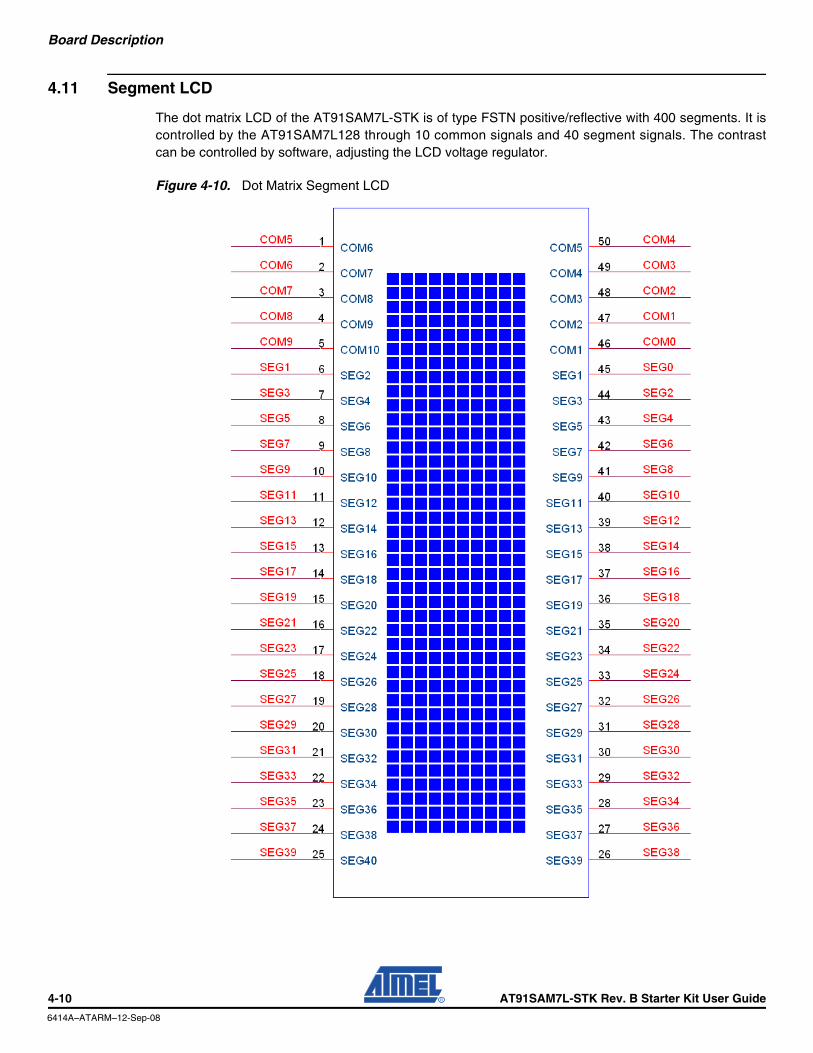
4.11 Segment LCD
The dot matrix LCD of the AT91SAM7L-STK is of type FSTN positive/reflective with 400 segments. It iscontrolled by the AT91SAM7L128 through 10 common signals and 40 segment signals. The contrastcan be controlled by software, adjusting the LCD voltage regulator.
Figure 4-10. Dot Matrix Segment LCD
4-10 AT91SAM7L-STK Rev. B Starter Kit User Guide
6414A–ATARM–12-Sep-08

Board Description
4.12 User Buttons
There are 5 user buttons on the AT91SAM7L-STK. The user buttons are connected to PIO lines anddefined as 4-direction and ok buttons by default.
Figure 4-11. User Buttons
AT91SAM7L-STK Rev. B Starter Kit User Guide 4-11
6414A–ATARM–12-Sep-08

Board Description
4.13 ZigBee
There is one ZigBee expansion interface for Atmel AT86RF230 ZigBee module. It is controlled via theSPI interface together with reset, interrupt and PIO control signals.
Figure 4-12. ZigBee Interface
Warning: The orientation of the connected circuit must be unambiguous. If the connected board isreversed, a short-circuit occurs between VCC and GND.
4-12 AT91SAM7L-STK Rev. B Starter Kit User Guide
6414A–ATARM–12-Sep-08

Board Description
4.14 PIO Expansion
The expansion connector of the AT91SAM7L-STK features the whole body of PIOC signals, ADC inputs,and ERASE pin. It enables users to expand functions such as SPI, TWI, PIO, ADC, USART, etc. WithERASE pin connected to VCC (short pin 39 and pin 40 by JS1), the internal Flash will be reinitializedupon system reset.
Figure 4-13. PIOC Expansion Connector
4.15 User Grids
The unassigned grid on the AT91SAM7L-STK is for users to implement their own small application cir-cuit on this board.
AT91SAM7L-STK Rev. B Starter Kit User Guide 4-13
6414A–ATARM–12-Sep-08

Section 5
Configuration
The pages that follow contain detailed descriptions of PIO usage, jumpers, test points and solder dropson the AT91SAM7L-STK.
5.1 PIO Usage
The AT91SAM7L128 microcontroller features three PIOs: PIOA, PIOB and PIOC.
All Segment LCD controller signals are on PIOA and PIOB.
PIOC and some of the PIOB IOs can be used fro peripheral signals such as SPI, TWI, PWM, USART,INT, etc.
AT91SAM7L-STK Rev. B Starter Kit User Guide 5-1
6414A–ATARM–12-Sep-08

Configuration
5.1.1 PIOA Usage on the AT91SAM7L-STK
Table 5-1. PIO Controller A
I/O Line Peripheral A Peripheral B Peripheral Usage Powered by
PA0 Segment LCD PANEL COM0 VDDIO2
PA1 Segment LCD PANEL COM1 VDDIO2
PA2 Segment LCD PANEL COM2 VDDIO2
PA3 Segment LCD PANEL COM3 VDDIO2
PA4 Segment LCD PANEL COM4 VDDIO2
PA5 Segment LCD PANEL COM5 VDDIO2
PA6 Segment LCD PANEL SEG0 VDDIO2
PA7 Segment LCD PANEL SEG1 VDDIO2
PA8 Segment LCD PANEL SEG2 VDDIO2
PA9 Segment LCD PANEL SEG3 VDDIO2
PA10 Segment LCD PANEL SEG4 VDDIO2
PA11 Segment LCD PANEL SEG5 VDDIO2
PA12 Segment LCD PANEL SEG6 VDDIO2
PA13 Segment LCD PANEL SEG7 VDDIO2
PA14 Segment LCD PANEL SEG8 VDDIO2
PA15 Segment LCD PANEL SEG9 VDDIO2
PA16 Segment LCD PANEL SEG10 VDDIO2
PA17 Segment LCD PANEL SEG11 VDDIO2
PA18 Segment LCD PANEL SEG12 VDDIO2
PA19 Segment LCD PANEL SEG13 VDDIO2
PA20 Segment LCD PANEL SEG14 VDDIO2
PA21 Segment LCD PANEL SEG15 VDDIO2
PA22 Segment LCD PANEL SEG16 VDDIO2
PA23 Segment LCD PANEL SEG17 VDDIO2
PA24 Segment LCD PANEL SEG18 VDDIO2
PA25 Segment LCD PANEL SEG19 VDDIO2
5-2 AT91SAM7L-STK Rev. B Starter Kit User Guide
6414A–ATARM–12-Sep-08

Configuration
5.1.2 PIOB Usage on the AT91SAM7L-STK
Table 5-2. PIO Controller B
I/O Line Peripheral A Peripheral B Peripheral Usage Powered by
PB0 Segment LCD PANEL SEG20 VDDIO2
PB1 Segment LCD PANEL SEG21 VDDIO2
PB2 Segment LCD PANEL SEG22 VDDIO2
PB3 Segment LCD PANEL SEG23 VDDIO2
PB4 Segment LCD PANEL SEG24 VDDIO2
PB5 Segment LCD PANEL SEG25 VDDIO2
PB6 Segment LCD PANEL SEG26 VDDIO2
PB7 Segment LCD PANEL SEG27 VDDIO2
PB8 Segment LCD PANEL SEG28 VDDIO2
PB9 Segment LCD PANEL SEG29 VDDIO2
PB10 Segment LCD PANEL SEG30 VDDIO2
PB11 Segment LCD PANEL SEG31 VDDIO2
PB12 NPCS3 Segment LCD PANEL SEG32 VDDIO2
PB13 NPCS2 Segment LCD PANEL SEG33 VDDIO2
PB14 NPCS1 Segment LCD PANEL SEG34 VDDIO2
PB15 RTS1 Segment LCD PANEL SEG35 VDDIO2
PB16 RTS0 Segment LCD PANEL SEG36 VDDIO2
PB17 DTR1 Segment LCD PANEL SEG37 VDDIO2
PB18 PWM0 Segment LCD PANEL SEG38 VDDIO2
PB19 PWM1 Segment LCD PANEL SEG39 VDDIO2
PB20 PWM2 Segment LCD PANEL COM6 VDDIO2
PB21 PWM3 Segment LCD PANEL COM7 VDDIO2
PB22 NPCS1 PCK1 Segment LCD PANEL COM8 VDDIO2
PB23 PCK0 NPCS3 Segment LCD PANEL COM9 VDDIO2
AT91SAM7L-STK Rev. B Starter Kit User Guide 5-3
6414A–ATARM–12-Sep-08

Configuration
5.1.3 PIOC Usage on the AT91SAM7L-STK
Table 5-3. PIO Controller C
I/O Line Peripheral A Peripheral B Peripheral Usage Powered by
PC0 CTS1 PWM2 User’s Input Buttons OK VDDIO1
PC1 DCD1 TIOA2 User’s Input Buttons UP VDDIO1
PC2 DTR1 TIOB2 User’s Input Buttons RIGHT VDDIO1
PC3 DSR1 TCLK1 User’s Input Buttons DOWN VDDIO1
PC4 RI1 TCLK2 User’s Input Buttons LEFT VDDIO1
PC5 IRQ1 NPCS2 ZigBee IRQ1 VDDIO1
PC6 NPCS1 PCK2 ZigBee NPCS1 VDDIO1
PC7 PWM0 TIOA0 MAX3318E FORCEOFF VDDIO1
PC8 PWM1 TIOB0 ZigBee RSIN VDDIO1
PC9 PWM2 SCK0 ZigBee SLP_IR VDDIO1
PC10 TWD NPCS3 VDDIO1
PC11 TWCK TCLK0 VDDIO1
PC12 RXD0 NPCS3 MAX3318E FORCEON VDDIO1
PC13 TXD0 PCK0 MAX3318E INVALID VDDIO1
PC14 RTS0 ADTRG MAX3318E READY VDDIO1
PC15 CTS0 PWM3 VCC/VBAT MONITOR ENABLE VDDIO1
PC16 DRXD NPCS1 MAX3318E DRXD VDDIO1
PC17 DTXD NPCS2 MAX3318E DTXD VDDIO1
PC18 NPCS0 PWM0 VDDIO1
PC19 MISO PWM1 ZigBee MISO VDDIO1
PC20 MOSI PWM2 ZigBee MOSI VDDIO1
PC21 SPCK PWM3 ZigBee SPCK VDDIO1
PC22 NPCS3 TIOA1 VDDIO1
PC23 PCK0 TIOB1 VDDIO1
PC24 RXD1 PCK1 VDDIO1
PC25 TXD1 PCK2 VDDIO1
PC26 RTS0 FIQ VDDIO1
PC27 NPCS2 IRQ0 VDDIO1
PC28 SCK1 PWM0 VDDIO1
PC29 RTS1 PWM1 VDDIO1
5-4 AT91SAM7L-STK Rev. B Starter Kit User Guide
6414A–ATARM–12-Sep-08

Configuration
5.2 Jumpers
Jumpers are used on the AT91SAM7L-STK for internal Flash Memory reinitialization and power currentmeasurement.
Notes: 1. This jumper is used to erase the internal Flash and the associated NVM bits of the AT91SAM7L device.2. This jumper is provided for enabling the AT91SAM7L128 chip power consumption measurement. By
default, it is closed. To use this feature, the user has to open the strap and insert an ammeter.3. This jumper is provided for the measurement of the whole AT91SAM7L-STK board power consumption.
By default, it is closed. To use this feature, the user has to open the strap and insert an ammeter.
5.3 Test Points
Some test points have been set on the AT91SAM7L-STK PCB in order to enable the monitoring of somerelevant signals.
Table 5-4. Jumpers on AT91SAM7L-STK
Designation Default Setting Feature
J6 pins 39-40 Opened Erase Internal Flash (1)
J8 Closed SAM7L VCC Jumper (2)
J9 Closed Board VCC Jumper (3)
Table 5-5. Test Points on AT91SAM7L-STK
Designation Description
TP1 RX (RS232 levels)
TP2 TX (RS232 levels)
TP3 CLKIN
TP4 FWUP
TP5 ADREF
TP6 XOUT
TP7 NRSTB
TP8 VDDIO2
TP9 VDD3V6
TP10 VDDOUT
AT91SAM7L-STK Rev. B Starter Kit User Guide 5-5
6414A–ATARM–12-Sep-08

Configuration
5.4 Solder Drops
Some solder drop selectors have been set on the AT91SAM7L-STK to enable alternate power supplyschemes, such as selecting the internal charge pump to be used, or not, for the Segment LCD controllersupply.
Table 5-6. Solder Drops on AT91SAM7L-STK
Designation Default Setting Feature
SD1 Opened Disables VDDIO2 to VDDLCD connection
SD2 2-3 Selects VCC or VDD3V6 to VDDLCD
SD3 Closed Enables VDDOUT applying to VDDCORE
SD4 2-3 Selects VDDINLCD input
5-6 AT91SAM7L-STK Rev. B Starter Kit User Guide
6414A–ATARM–12-Sep-08

Section 6
Schematics
This section contains the following schematics:
Top Level Synoptic
Interface
LCD, KBD
Processor
AT91SAM7L-STK Rev. B Starter Kit User Guide 6-1
6414A–ATARM–12-Sep-08

8
8
7
7
6
6
5
5
4
4
3
3
2
2
1
1
D D
C C
B B
A A
PC[0..29]
PB[0..23]
PA[0..25]
PC[0..29]
AD[0..3]
PC[0..29]
AD[0..3]
PA[0..25]
PB[0..23]
REV DATEMODIF. DES. DATE VER.
SCALE 1/1 REV. SHEET
This agreement is our property. Reproduction and publication without our written authorization shall expose offender to legal proceedings.
INIT EDITA
AT91SAM7L-STK14B
XX-XXX-XXPP XXX
Top level
17MAR08B 18-APR-08PP 18-APR-08LLE
REV DATEMODIF. DES. DATE VER.
SCALE 1/1 REV. SHEET
This agreement is our property. Reproduction and publication without our written authorization shall expose offender to legal proceedings.
INIT EDITA
AT91SAM7L-STK14B
XX-XXX-XXPP XXX
Top level
17MAR08B 18-APR-08PP 18-APR-08LLE
REV DATEMODIF. DES. DATE VER.
SCALE 1/1 REV. SHEET
This agreement is our property. Reproduction and publication without our written authorization shall expose offender to legal proceedings.
INIT EDITA
AT91SAM7L-STK14B
XX-XXX-XXPP XXX
Top level
17MAR08B 18-APR-08PP 18-APR-08LLE
SHEET 2
SHEET 4
SHEET 3
����
�����
����
Processor
Processor
PB[0..23]
PA[0..25]
PC[0..29]
AD[0..3]
ERASE
LCD, KBD
LCD, KBD
PC[0..29]
PB[0..23]
PA[0..25]
AD[0..3]
ERASE
Interfaces
Interfaces
PC[0..29]

8
8
7
7
6
6
5
5
4
4
3
3
2
2
1
1
D D
C C
B B
A A
PC19
PC0PC1PC2PC3PC4PC5PC6PC7PC8PC9PC10PC11PC12PC13PC14PC15PC16PC17PC18PC19PC20PC21PC22PC23PC24PC25PC26PC27PC28PC29
PC8
PC21
PC5
PC6PC20PC9
PC17
PC16
PC13
PC14 PC12
PC7
PC27
PC[0..29]
VCC VCC
VCC
VCC
VCC
VCCVCC
VCC
GND
GND
GNDGND
GND
GND
GNDVCC
GND
GND
VCC
GND
GND
GND GND
VCC
REV DATEMODIF. DES. DATE VER.
SCALE 1/1 REV. SHEET
This agreement is our property. Reproduction and publication without our written authorization shall expose offender to legal proceedings.
INIT EDITA
AT91SAM7L-STK24B
XX-XXX-XXPP XXX
Interfaces
17MAR08B 18-APR-08PP 18-APR-08LLE
REV DATEMODIF. DES. DATE VER.
SCALE 1/1 REV. SHEET
This agreement is our property. Reproduction and publication without our written authorization shall expose offender to legal proceedings.
INIT EDITA
AT91SAM7L-STK24B
XX-XXX-XXPP XXX
Interfaces
17MAR08B 18-APR-08PP 18-APR-08LLE
REV DATEMODIF. DES. DATE VER.
SCALE 1/1 REV. SHEET
This agreement is our property. Reproduction and publication without our written authorization shall expose offender to legal proceedings.
INIT EDITA
AT91SAM7L-STK24B
XX-XXX-XXPP XXX
Interfaces
17MAR08B 18-APR-08PP 18-APR-08LLE
ZIGBEE INTERFACE
Note: Pin 1 on Zigbee board RZ502 matches pin 2 on this connector
MISOSPCKNPSC1
RSTN
IRQ1
MOSISLP_TR
SERIAL DEBUG PORT
Only for AT86RF230Rev.A connexionnot required for Rev.B on
DTXD
DRXD
TX
RX
BATTERY JUMPER
IRQ0
TP2TESTPOINT
TP2TESTPOINT
R3NOT POPULATEDR3NOT POPULATED
TP1TESTPOINTTP1TESTPOINT
C1100NFC1100NF
C6NOT POPULATEDC6NOT POPULATED
C3100NFC3100NF
U2
NC7SZ175P6XNOT POPULATED
U2
NC7SZ175P6XNOT POPULATED
CP1
GND 2
D3
Q 4
VCC 5
C6
J4
D09P24A4GX00
J4
D09P24A4GX00
5
4
3
2
1
9
8
7
6
1011
C2100NFC2100NF
AAA
AAA
J1
AAA
AAA
J1
J5J5
1 23 45 67 89 10
11 1213151719
14161820
21 2223 2425 2627 2829 3031 3233 3435 3637 3839 40
R5 0RR5 0R
J3PadJ3Pad
11
R4NOT POPULATEDR4NOT POPULATED
R710KR710K
R2NOT POPULATEDR2NOT POPULATED
R2510MR2510M
R1NOT POPULATEDR1NOT POPULATED
C5100NFC5100NF
C7NOT POPULATEDC7NOT POPULATED
J2PadJ2Pad
11
J9J9
U1
MAX3318E
U1
MAX3318E
READY 1
C1+ 2
C1- 4
C2+ 5
C2- 6
VCC19
GND18
V+3
V-7
R1IN16
R2IN9
R1OUT 15
R2OUT 10
INVALID 11
FORCEOFF 20
FORCEON 14
D1OUT17
D2OUT8
D1IN 13
D2IN 12
C4100NFC4100NF
R6 0RR6 0R
U3
NC7SZ125P5XNOT POPULATED
U3
NC7SZ125P5XNOT POPULATED
2 4
35
1
JS3JS3

8
8
7
7
6
6
5
5
4
4
3
3
2
2
1
1
D D
C C
B B
A A
PA5 COM5
PA10 SEG4
PA7 SEG1
PA3 COM3
PA19 SEG13
PA16 SEG10
PA21 SEG15
PA17 SEG11
PA15 SEG9
PA0 COM0
PA18 SEG12
PA24 SEG18
PA20 SEG14
PA23 SEG17PA22 SEG16
PA9 SEG3
PA12 SEG6
PA6 SEG0
PA1 COM1
PA8 SEG2
PA14 SEG8
PA4 COM4
PA13 SEG7
PA11 SEG5
PA25 SEG19
PA2 COM2 PB2 SEG22PB1 SEG21
PB5 SEG25PB4 SEG24PB3 SEG23
PB0 SEG20
PB7 SEG27
PB13 SEG33
PB8 SEG28
PB12 SEG32
PB9 SEG29
PB17 SEG37PB16 SEG36
PB10 SEG30
PB6 SEG26
PB15 SEG35PB14 SEG34
PB11 SEG31
PB21 COM7
PB23 COM9
PB19 SEG39
PB22 COM8
PB20 COM6
PB18 SEG38
PC2PC3
PC0
PC4
PC1
PC10PC11
PC25PC26PC27PC28PC29
PC5PC6PC7PC8PC9
PC12PC13PC14PC15PC16PC17PC18PC19PC20PC21PC22PC23PC24
PC1
PC4
PC3
PC28PC29
PC23PC21
PC17
PC25PC27
PC3PC1
PC13PC11
PC7
PC15
PC5
PC9
PC19
PC24PC26
PC18PC16
PC22PC20
PC4PC2PC0
PC14PC12PC10PC8PC6
AD3AD2AD1AD0
AD1AD3
AD0AD2
ERASE
CO
M4
CO
M3
CO
M2
CO
M1
CO
M0
SE
G0
SE
G2
SE
G4
SE
G6
SE
G8
SE
G10
SE
G12
SE
G22
SE
G24
SE
G26
SE
G28
SE
G30
SE
G32
SE
G34
SE
G36
SE
G14
SE
G16
SE
G18
SE
G20
CO
M9
SE
G1
SE
G3
SE
G5
SE
G7
SE
G9
SE
G11
SE
G13
CO
M5
CO
M6
CO
M7
CO
M8
SE
G23
SE
G25
SE
G27
SE
G29
SE
G31
SE
G33
SE
G35
SE
G37
SE
G15
SE
G17
SE
G19
SE
G21
SE
G38
SE
G39
PC15
AD3
PC0
PC2
PC[0..29]
PB[0..23]
PA[0..25]
AD[0..3]
ERASE
AD[0..3]
VCC
GNDGND
VCC
GND
VCC
GND
VCC VCC
GND GND GND
REV DATEMODIF. DES. DATE VER.
SCALE 1/1 REV. SHEET
This agreement is our property. Reproduction and publication without our written authorization shall expose offender to legal proceedings.
INIT EDITA
AT91SAM7L-STK34B
XX-XXX-XXPP XXX
LCD, KBD
17MAR08B 18-APR-08PP 18-APR-08LLE
REV DATEMODIF. DES. DATE VER.
SCALE 1/1 REV. SHEET
This agreement is our property. Reproduction and publication without our written authorization shall expose offender to legal proceedings.
INIT EDITA
AT91SAM7L-STK34B
XX-XXX-XXPP XXX
LCD, KBD
17MAR08B 18-APR-08PP 18-APR-08LLE
REV DATEMODIF. DES. DATE VER.
SCALE 1/1 REV. SHEET
This agreement is our property. Reproduction and publication without our written authorization shall expose offender to legal proceedings.
INIT EDITA
AT91SAM7L-STK34B
XX-XXX-XXPP XXX
LCD, KBD
17MAR08B 18-APR-08PP 18-APR-08LLE
VCC/VBAT MONITOR
UP
OK
RIGHT
LEFT
DOWNOKUPRIGHT
LEFTDOWN
CTS1/PWM2_WKUP0DCD1/TIOA2_WKUP1DTR1/TIOB2_WKUP2DSR1/TCLK1_WKUP3RI1/TCLK2_WKUP4IRQ1/NPCS2_WKUP5NPCS1/PCK2_WKUP6PWM0/TIOA0PWM1/TIOB0PWM2/SCK0TWD/NPCS3TWCK/TCLK0_WKUP7RXD0/NPCS3_WKUP8TXD0/PCK0_WKUP9RTS0/ADTRG_WKUP10CTS0/PWM3_WKUP11DRXD/NPCS1/DTXD/MPCS2NPCS0/PWM0MISO/PWM1MOSI/PWM2SPCK/PWM3MPCS3/TIOA1PCK0/TIOB1RXD1/PCK1TXD1/PCK2RTS0/FIQ_WKUP12NPCS2/IRQ0_WKUP13SCK1/PWM0_WKUP14RTS1/PWM1_WKUP15
PCK0/NPCS3
NPCS3NPCS2NPCS1RTS1RTS0DTR1PWM0PWM1PWM2PWM3NPSC1/PCK1
R26 100KR26 100K
UG11UG11UG42UG42
UG1UG1
UG7UG7UG38UG38
R11NOT POPULATEDR11NOT POPULATED
UG3UG3UG34UG34
BP4
3-1437565-0
BP4
3-1437565-0
LCD1
LCD_GS08001AA
LCD1
LCD_GS08001AA
CO
M5
50
CO
M4
49
CO
M3
48
CO
M2
47
CO
M1
46
SE
G1
45
SE
G3
44
SE
G5
43
SE
G7
42
SE
G9
41
SE
G11
40
SE
G13
39
SE
G15
38
SE
G17
37
SE
G19
36
SE
G21
35
SE
G23
34
SE
G25
33
SE
G27
32
SE
G29
31
SE
G31
30
SE
G33
29
SE
G35
28
SE
G37
27
SE
G39
26S
EG
4025
SE
G38
24
CO
M6
1
CO
M7
2
CO
M8
3
CO
M9
4
CO
M10
5
SE
G2
6
SE
G4
7
SE
G6
8
SE
G8
9
SE
G10
10
SE
G12
11
SE
G14
12
SE
G16
13
SE
G18
14
SE
G20
15
SE
G22
16
SE
G24
17
SE
G26
18
SE
G28
19
SE
G30
20
SE
G32
21
SE
G34
22
SE
G36
23
UG43UG43
UG8UG8UG39UG39
BP1
3-1437565-0
BP1
3-1437565-0
UG4UG4UG35UG35
BP5
3-1437565-0
BP5
3-1437565-0
UG9UG9UG40UG40
JS1JS1
UG5UG5UG36UG36
BP2
3-1437565-0
BP2
3-1437565-0
Q1FDV304PQ1FDV304P
1
32
R9
10K
R9
10K
UG2UG2
UG10UG10UG41UG41
UG6UG6UG37UG37
J6J6
1 23 45 67 89 10
11 1213151719
14161820
21 2223 2425 2627 2829 3031 3233 3435 3637 3839 40
UG33UG33
R10NOT POPULATEDR10NOT POPULATED
BP3
3-1437565-0
BP3
3-1437565-0
R8
10K
R8
10K

8
8
7
7
6
6
5
5
4
4
3
3
2
2
1
1
D D
C C
B B
A A
PC
16
PC
19P
C18
PC
17
PC
20
PC
22P
C21
PC
23
PC
5P
C6
PC
2
PC
9
PC
3
PC
0
PC
4
PC
8P
C7
PC
1
PC
10
PC
15P
C14
PC
12P
C11
PC
13
PC
24P
C25
PC
26P
C27
PC
28P
C29
PA5
PA10
PA7
PA3
PA19
PA16
PA21
PA17
PA15
PA0
PA18
PA24
PA20
PA23PA22
PA9
PA12
PA6
PA1
PA8
PA14
PA4
PA13
PA11
PA25
PA2
AD3AD2AD1AD0
PB2PB1
PB5PB4PB3
PB0
PB7
PB13
PB8
PB12
PB9
PB17PB16
PB10
PB6
PB15PB14
PB11
PB21
PB23
PB19
PB22
PB20
PB18
VD
DO
UT
ERASE
VDDOUT
JTAG_TDIJTAG_TMSJTAG_TCK
JTAG_RSTJTAG_TDO
PB[0..23]
PA[0..25]
PC[0..29]
AD[0..3]
ERASE
VCC
VCC
VCC
VCC
VCC
VCC
GND
GND
GND
GND
GND
GND
GND
GND
GND
VCC
REV DATEMODIF. DES. DATE VER.
SCALE 1/1 REV. SHEET
This agreement is our property. Reproduction and publication without our written authorization shall expose offender to legal proceedings.
INIT EDITA
AT91SAM7L-STK44B
XX-XXX-XXPP XXX
Processor
17MAR08B 18-APR-08PP 18-APR-08LLE
REV DATEMODIF. DES. DATE VER.
SCALE 1/1 REV. SHEET
This agreement is our property. Reproduction and publication without our written authorization shall expose offender to legal proceedings.
INIT EDITA
AT91SAM7L-STK44B
XX-XXX-XXPP XXX
Processor
17MAR08B 18-APR-08PP 18-APR-08LLE
REV DATEMODIF. DES. DATE VER.
SCALE 1/1 REV. SHEET
This agreement is our property. Reproduction and publication without our written authorization shall expose offender to legal proceedings.
INIT EDITA
AT91SAM7L-STK44B
XX-XXX-XXPP XXX
Processor
17MAR08B 18-APR-08PP 18-APR-08LLE
FORCE WAKE-UP
FWKUP
NRSTB
RESET
ICE INTERFACE
SAM7L INPUT CURRENT
C26
100N
FC
2610
0NF
R22
10K
R22
10K
C16220NFC16220NF
C10
22NF
C10
22NF
SD3
SOLDER DROP 2 pins closed
SD3
SOLDER DROP 2 pins closed
11 2 2
R2410RR2410R
C1218PFC1218PF
TP6TESTPOINTTP6TESTPOINT
C28
100N
FC
2810
0NF
C33
6V310µF
C33
6V310µF
J8J8
R13100KR13100K
TP7TESTPOINTTP7TESTPOINT
C23
100N
FC
2310
0NF
C11
2.2NF
C11
2.2NF
BP63-1437565-0BP63-1437565-0
C32
100N
FC
3210
0NF
C8NOT POPULATEDC8NOT POPULATED
C24
100N
FC
2410
0NF
R19NOT POPULATEDR19NOT POPULATED
SD2
SOLDER DROP 3 pins
SD2
SOLDER DROP 3 pins
1 2
3
C20
100N
FC
2010
0NF
J7J7
12345678910111213151719
14161820
R23
NOT POPULATED
R23
NOT POPULATED
TP3TESTPOINTTP3TESTPOINT
TP4TESTPOINTTP4TESTPOINT
TP8
TESTPOINT
TP8
TESTPOINT
C27
6V3
10µF
C27
6V3
10µF
C19
100N
FC
1910
0NF
R12100KR12100K
C22
100N
FC
2210
0NF
C17
2.2µ
FC
172.
2µF
C30100NFC30100NF
C31
100N
FC
3110
0NF
C34
6V310µFC34
6V310µF C
1810
0NF
C18
100N
FTP9
TESTPOINT
TP9
TESTPOINT
R21
NOT POPULATED
R21
NOT POPULATED
R14180RR14180R
R16100KR16100K
C25
100N
FC
2510
0NF
R18100KR18100K
SD4SOLDER DROP 3 pinsSD4SOLDER DROP 3 pins
12
3
R17100KR17100K
C21
100N
FC
2110
0NF
C1410NFC1410NF
JS2JS2
R15100KR15100K
C29
6V310µFC29
6V310µF
BP73-1437565-0BP73-1437565-0
XC1 32.768 kHz
CM415-32.768KDZFB-F
XC1 32.768 kHz
CM415-32.768KDZFB-F
1 2
TP5
TESTPOINT
TP5
TESTPOINT
C15220NFC15220NF
SD1
SOLDER DROP 2 pins open
SD1
SOLDER DROP 2 pins open
11
22
AT91SAM7L-LQFP128
U4 AT91SAM7L128-AU
AT91SAM7L-LQFP128
U4 AT91SAM7L128-AU
PA0_COM0 3
PA1_COM1 4
PA2_COM2 5
PA3_COM3 6
PA4_COM4 7
PA5_COM5 8
PA6_SEG0 9
PA7_SEG1 10
PA8_SEG2 11
PA9_SEG3 12
PA10_SEG4 13
PA11_SEG5 16
PA12_SEG6 17
PA13_SEG7 18
PA14_SEG8 19
PA15_SEG9 20
PA16_SEG10 21
PA17_SEG11 22
PA18_SEG12 23
PA19_SEG13 24
PA20_SEG14 25
PA21_SEG15 26
PA22_SEG16 27
TCK81
TDO117
TDI116
TMS82
PA23_SEG17 29
VD
DC
OR
E62
VD
DC
OR
E10
0
VD
DC
OR
E2
JTAGSEL83
GN
D14
GN
D76
GN
D40
GN
D12
0G
ND
86
GN
D56
GN
D68
VD
DIO
215
VD
DIO
232
VD
DIO
255
VD
DIO
185
VD
DIO
111
9
VD
DIN
LCD
39
XOUT128
XIN/PGMCK127
PLLRC121
FWUP118
CLKIN125
NRST79
VD
DC
OR
E28
VD
DC
OR
E84
ADVREF 69
PA25_SEG19 31PA24_SEG18 30
AD3 70
AD2 71
AD1 72
AD0 73
PB0_SEG2041
PB1_SEG2142
PB2_SEG2243
PB3_SEG2344
PB4_SEG2445
PB5_SEG2546
PB6_SEG2647
PB7_SEG2748
PB8_SEG2849
PB9_SEG2950
PB10_SEG3051
PB11_SEG3152
PB12/NPCS3_SEG3253
PB13/NPCS2_SEG3354
PB14/NPCS1_SEG3457
PB15/RTS1_SEG3558
PB16/RTS0_SEG3659
PB17/DTR1_SEG3760
PB18/PWM0_SEG3861
PB19/PWM1_SEG3963
PB20/PWM2_COM664
PB21/PWM3_COM765
PB22/NPSC1/PCK1_COM866
PB23/PCK0/NPCS3_COM967
PC
0/C
TS1/
PW
M2_
WK
UP
087
PC
1/D
CD
1/TI
OA
2_W
KU
P1
88
PC
2/D
TR1/
TIO
B2_
WK
UP
289
PC
3/D
SR
1/TC
LK1_
WK
UP
390
PC
4/R
I1/T
CLK
2_W
KU
P4
91
PC
5/IR
Q1/
NP
CS
2_W
KU
P5
92
PC
6/N
PC
S1/
PC
K2_
WK
UP
693
PC
7/P
WM
0/TI
OA
094
PC
8/P
WM
1/TI
OB
095
PC
9/P
WM
2/S
CK
096
PC
10/T
WD
/NP
CS
397
PC
11/T
WC
K/T
CLK
0_W
KU
P7
98
PC
12/R
XD
0/N
PC
S3_
WK
UP
899
PC
13/T
XD
0/P
CK
0_W
KU
P9
101
PC
14/R
TS0/
AD
TRG
_WK
UP
1010
2
PC
15/C
TS0/
PW
M3_
WK
UP
1110
3
PC
16/D
RX
D/N
PC
S1
104
PC
17/D
TXD
/MP
CS
210
5
PC
18/N
PC
S0/
PW
M0
106
PC
19/M
ISO
/PW
M1
107
PC
20/M
OS
I/PW
M2
108
PC
21/S
PC
K/P
WM
310
9
PC
22/M
PC
S3/
TIO
A1
110
PC
23/P
CK
0/TI
OB
111
1
TST 1
ER
AS
E80
PC
24/R
XD
1/P
CK
111
2
PC
25/T
XD
1/P
CK
211
3
PC
26/R
TS0/
FIQ
_WK
UP
1211
4
PC
27/N
PC
S2/
IRQ
0_W
KU
P13
115
PC
28/S
CK
1/P
WM
0_W
KU
P14
77
PC
29/R
TS1/
PW
M1_
WK
UP
1578
VD
DC
OR
E12
4
VD
DIO
175
VD
DO
UT
74
VD
DLC
D33
VD
D3V
634
NRSTB 126
PLLRCGND122
GNDPLL123
CA
PM
235
CA
PP
236
CA
PM
137
CA
PP
138
R20 0RR20 0R
C9100NFC9100NF
TP10
TESTPOINT
TP10
TESTPOINT
C1318PFC1318PF

AT91SAM7L-STK Rev. B Starter Kit User Guide 7-1
6414A–ATARM–12-Sep-08
Section 7
Revision History
Doc Rev CommentsChange Request Ref.
6409A First issue.

6414A–ATARM–12-Sep-08
Headquarters International
Atmel Corporation2325 Orchard ParkwaySan Jose, CA 95131USATel: 1(408) 441-0311Fax: 1(408) 487-2600
Atmel AsiaRoom 1219Chinachem Golden Plaza77 Mody Road TsimshatsuiEast KowloonHong KongTel: (852) 2721-9778Fax: (852) 2722-1369
Atmel EuropeLe Krebs8, Rue Jean-Pierre TimbaudBP 30978054 Saint-Quentin-en-Yvelines CedexFranceTel: (33) 1-30-60-70-00 Fax: (33) 1-30-60-71-11
Atmel Japan9F, Tonetsu Shinkawa Bldg.1-24-8 ShinkawaChuo-ku, Tokyo 104-0033JapanTel: (81) 3-3523-3551Fax: (81) 3-3523-7581
Product Contact
Web Sitewww.atmel.comwww.atmel.com/AT91SAM
Technical SupportAT91SAM SupportAtmel techincal support
Sales Contactswww.atmel.com/contacts/
Literature Requestswww.atmel.com/literature
Disclaimer: The information in this document is provided in connection with Atmel products. No license, express or implied, by estoppel or otherwise, to anyintellectual property right is granted by this document or in connection with the sale of Atmel products. EXCEPT AS SET FORTH IN ATMEL’S TERMS AND CONDI-TIONS OF SALE LOCATED ON ATMEL’S WEB SITE, ATMEL ASSUMES NO LIABILITY WHATSOEVER AND DISCLAIMS ANY EXPRESS, IMPLIED OR STATUTORYWARRANTY RELATING TO ITS PRODUCTS INCLUDING, BUT NOT LIMITED TO, THE IMPLIED WARRANTY OF MERCHANTABILITY, FITNESS FOR A PARTICULARPURPOSE, OR NON-INFRINGEMENT. IN NO EVENT SHALL ATMEL BE LIABLE FOR ANY DIRECT, INDIRECT, CONSEQUENTIAL, PUNITIVE, SPECIAL OR INCIDEN-TAL DAMAGES (INCLUDING, WITHOUT LIMITATION, DAMAGES FOR LOSS OF PROFITS, BUSINESS INTERRUPTION, OR LOSS OF INFORMATION) ARISING OUT OFTHE USE OR INABILITY TO USE THIS DOCUMENT, EVEN IF ATMEL HAS BEEN ADVISED OF THE POSSIBILITY OF SUCH DAMAGES. Atmel makes norepresentations or warranties with respect to the accuracy or completeness of the contents of this document and reserves the right to make changes to specificationsand product descriptions at any time without notice. Atmel does not make any commitment to update the information contained herein. Unless specifically providedotherwise, Atmel products are not suitable for, and shall not be used in, automotive applications. Atmel’s products are not intended, authorized, or warranted for useas components in applications intended to support or sustain life.
© 2008 Atmel Corporation. All rights reserved. Atmel®, Atmel logo and combinations thereof, SAM-BA® and others are registered trademarks ortrademarks of Atmel Corporation or its subsidiaries. ARM®, ARMPowered® logo and others are registered trademarks or trademarks of ARM Ltd.Other terms and product names may be trademarks of others.