
ARM 7 & ARM 9 MICROCONTROLLERS AT91 1 AT91RM9200 Embedded Peripherals.

AT91 ARM Thumb-based Microcontrollers
AT91SAM7X512AT91SAM7X256 AT91SAM7X128
Preliminary
6120F–ATARM–03-Oct-06
Features• Incorporates the ARM7TDMI® ARM® Thumb® Processor
– High-performance 32-bit RISC Architecture– High-density 16-bit Instruction Set
– Leader in MIPS/Watt– EmbeddedICE™ In-circuit Emulation, Debug Communication Channel Support
• Internal High-speed Flash – 512 Kbytes (AT91SAM7X512) Organized in Two Banks of 1024 Pages of
256 Bytes (Dual Plane)– 256 Kbytes (AT91SAM7X256) Organized in 1024 Pages of 256 Bytes (Single Plane)– 128 Kbytes (AT91SAM7X128) Organized in 512 Pages of 256 Bytes (Single Plane)
– Single Cycle Access at Up to 30 MHz in Worst Case Conditions– Prefetch Buffer Optimizing Thumb Instruction Execution at Maximum Speed– Page Programming Time: 6 ms, Including Page Auto-erase,
Full Erase Time: 15 ms– 10,000 Write Cycles, 10-year Data Retention Capability,
Sector Lock Capabilities, Flash Security Bit– Fast Flash Programming Interface for High Volume Production
• Internal High-speed SRAM, Single-cycle Access at Maximum Speed– 128 Kbytes (AT91SAM7X512)– 64 Kbytes (AT91SAM7X256)– 32 Kbytes (AT91SAM7X128)
• Memory Controller (MC)– Embedded Flash Controller, Abort Status and Misalignment Detection
• Reset Controller (RSTC)– Based on Power-on Reset Cells and Low-power Factory-calibrated Brownout
Detector– Provides External Reset Signal Shaping and Reset Source Status
• Clock Generator (CKGR)– Low-power RC Oscillator, 3 to 20 MHz On-chip Oscillator and one PLL
• Power Management Controller (PMC)– Power Optimization Capabilities, Including Slow Clock Mode (Down to 500 Hz) and
Idle Mode– Four Programmable External Clock Signals
• Advanced Interrupt Controller (AIC)– Individually Maskable, Eight-level Priority, Vectored Interrupt Sources– Two External Interrupt Sources and One Fast Interrupt Source, Spurious Interrupt
Protected• Debug Unit (DBGU)
– 2-wire UART and Support for Debug Communication Channel interrupt, Programmable ICE Access Prevention
• Periodic Interval Timer (PIT)– 20-bit Programmable Counter plus 12-bit Interval Counter
• Windowed Watchdog (WDT)– 12-bit key-protected Programmable Counter– Provides Reset or Interrupt Signals to the System– Counter May Be Stopped While the Processor is in Debug State or in Idle Mode
• Real-time Timer (RTT)– 32-bit Free-running Counter with Alarm– Runs Off the Internal RC Oscillator

• Two Parallel Input/Output Controllers (PIO) – Sixty-two Programmable I/O Lines Multiplexed with up to Two Peripheral I/Os – Input Change Interrupt Capability on Each I/O Line– Individually Programmable Open-drain, Pull-up Resistor and Synchronous Output
• Thirteen Peripheral DMA Controller (PDC) Channels• One USB 2.0 Full Speed (12 Mbits per second) Device Port
– On-chip Transceiver, 1352-byte Configurable Integrated FIFOs• One Ethernet MAC 10/100 base-T
– Media Independent Interface (MII) or Reduced Media Independent Interface (RMII)– Integrated 28-byte FIFOs and Dedicated DMA Channels for Transmit and Receive
• One Part 2.0A and Part 2.0B Compliant CAN Controller– Eight Fully-programmable Message Object Mailboxes, 16-bit Time Stamp Counter
• One Synchronous Serial Controller (SSC)– Independent Clock and Frame Sync Signals for Each Receiver and Transmitter– I²S Analog Interface Support, Time Division Multiplex Support– High-speed Continuous Data Stream Capabilities with 32-bit Data Transfer
• Two Universal Synchronous/Asynchronous Receiver Transmitters (USART)– Individual Baud Rate Generator, IrDA® Infrared Modulation/Demodulation– Support for ISO7816 T0/T1 Smart Card, Hardware Handshaking, RS485 Support– Full Modem Line Support on USART1
• Two Master/Slave Serial Peripheral Interfaces (SPI)– 8- to 16-bit Programmable Data Length, Four External Peripheral Chip Selects
• One Three-channel 16-bit Timer/Counter (TC)– Three External Clock Inputs, Two Multi-purpose I/O Pins per Channel– Double PWM Generation, Capture/Waveform Mode, Up/Down Capability
• One Four-channel 16-bit Power Width Modulation Controller (PWMC)• One Two-wire Interface (TWI)
– Master Mode Support Only, All Two-wire Atmel EEPROMs Supported• One 8-channel 10-bit Analog-to-Digital Converter, Four Channels Multiplexed with Digital I/Os• SAM-BA™ Boot Assistance
– Default Boot program– Interface with SAM-BA Graphic User Interface
• IEEE® 1149.1 JTAG Boundary Scan on All Digital Pins• 5V-tolerant I/Os, Including Four High-current Drive I/O lines, Up to 16 mA Each• Power Supplies
– Embedded 1.8V Regulator, Drawing up to 100 mA for the Core and External Components– 3.3V VDDIO I/O Lines Power Supply, Independent 3.3V VDDFLASH Flash Power Supply– 1.8V VDDCORE Core Power Supply with Brownout Detector
• Fully Static Operation: Up to 55 MHz at 1.65V and 85°C Worst Case Conditions• Available in 100-lead LQFP Green and 100-ball TFBGA Green Packages
26120F–ATARM–03-Oct-06
AT91SAM7X512/256/128 Preliminary
AT91SAM7X512/256/128 Preliminary
1. DescriptionAtmel's AT91SAM7X512/256/128 is a member of a series of highly integrated Flash microcon-trollers based on the 32-bit ARM RISC processor. It features 512/256/128 Kbyte high-speed Flash and 128/64/32 Kbyte SRAM, a large set of peripherals, including an 802.3 Ethernet MAC and a CAN controller. A complete set of system functions minimizes the number of external components.
The embedded Flash memory can be programmed in-system via the JTAG-ICE interface or via a parallel interface on a production programmer prior to mounting. Built-in lock bits and a secu-rity bit protect the firmware from accidental overwrite and preserve its confidentiality.
The AT91SAM7X512/256/128 system controller includes a reset controller capable of managing the power-on sequence of the microcontroller and the complete system. Correct device opera-tion can be monitored by a built-in brownout detector and a watchdog running off an integrated RC oscillator.
By combining the ARM7TDMI processor with on-chip Flash and SRAM, and a wide range of peripheral functions, including USART, SPI, CAN Controller, Ethernet MAC, Timer Counter, RTT and Analog-to-Digital Converters on a monolithic chip, the AT91SAM7X512/256/128 is a power-ful device that provides a flexible, cost-effective solution to many embedded control applications requiring communication over, for example, Ethernet, CAN wired and Zigbee™ wireless networks.
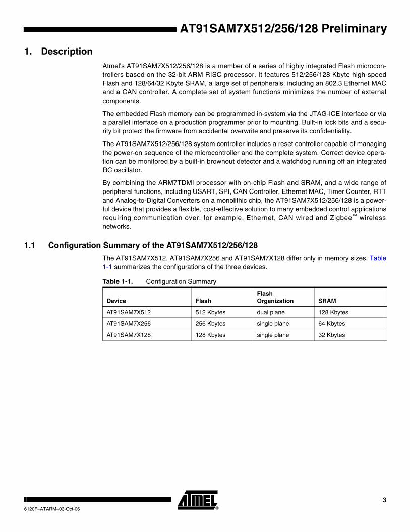
1.1 Configuration Summary of the AT91SAM7X512/256/128
The AT91SAM7X512, AT91SAM7X256 and AT91SAM7X128 differ only in memory sizes. Table 1-1 summarizes the configurations of the three devices.
Table 1-1. Configuration Summary
Device FlashFlash Organization SRAM
AT91SAM7X512 512 Kbytes dual plane 128 Kbytes
AT91SAM7X256 256 Kbytes single plane 64 Kbytes
AT91SAM7X128 128 Kbytes single plane 32 Kbytes
36120F–ATARM–03-Oct-06

2. AT91SAM7X512/256/128 Block Diagram
Figure 2-1. AT91SAM7X512/256/128 Block Diagram
TDITDOTMSTCK
NRST
FIQ
IRQ0-IRQ1
PCK0-PCK3
PMC
Peripheral Bridge
Peripheral DMAController
AIC
PLL
RCOSC
SRAM128/64/32 Kbytes
ARM7TDMI Processor
ICEJTAGSCAN
JTAGSEL
PIOA
USART0
SSC
Timer Counter
RXD0TXD0SCK0RTS0CTS0
SPI0_NPCS0SPI0_NPCS1SPI0_NPCS2SPI0_NPCS3
SPI0_MISOSPI0_MOSISPI0_SPCK
Flash512/256/128
Kbytes
ResetController
DRXDDTXD
TFTKTDRDRKRFTCLK0TCLK1TCLK2TIOA0TIOB0TIOA1TIOB1TIOA2TIOB2
Memory Controller
AbortStatus
AddressDecoder
MisalignmentDetection
PIO
PIO
APB
POR
EmbeddedFlash
Controllers
AD0AD1AD2AD3
ADTRG
PLLRC
13 Channels
PDC
PDC
USART1
RXD1TXD1SCK1RTS1CTS1DCD1DSR1DTR1
RI1
PDC
PDC
PDC
PDC
SPI0
PDC
ADC
ADVREF
PDC
PDC
TC0
TC1
TC2
TWDTWCKTWI
OSCXINXOUT
VDDIN
PWMCPWM0PWM1PWM2PWM3
1.8 VVoltage
Regulator
USB DeviceFIFO
DDMDDP
Tran
scei
ver
GNDVDDOUT
BOD
VDDCORE
VDDCOREVDDFLASH
AD4AD5AD6AD7
VDDFLASH
Fast Flash Programming
Interface
ERASE
PIO
PGMD0-PGMD15PGMNCMDPGMEN0-PGMEN1
PGMRDYPGMNVALIDPGMNOEPGMCKPGMM0-PGMM3
VDDIO
TST
DBGUPDC
PDC
PIT
WDT
RTT
System Controller
VDDCORE
CANCANRXCANTX
PIOEthernet MAC 10/100
ETXCK-ERXCK-EREFCKETXEN-ETXERECRS-ECOL, ECRSDVERXER-ERXDVERX0-ERX3ETX0-ETX3EMDCEMDIO
DMA
FIFOPIOB
SPI1_NPCS0SPI1_NPCS1SPI1_NPCS2SPI1_NPCS3
SPI1_MISOSPI1_MOSISPI1_SPCK
PDC
PDC
SPI1
EF100
SAM-BA
ROM
VDDFLASH
46120F–ATARM–03-Oct-06
AT91SAM7X512/256/128 Preliminary

AT91SAM7X512/256/128 Preliminary
3. Signal Description
Table 3-1. Signal Description List
Signal Name Function TypeActive Level Comments
Power
VDDINVoltage Regulator and ADC Power Supply Input
Power 3V to 3.6V
VDDOUT Voltage Regulator Output Power 1.85V
VDDFLASH Flash and USB Power Supply Power 3V to 3.6V
VDDIO I/O Lines Power Supply Power 3V to 3.6V
VDDCORE Core Power Supply Power 1.65V to 1.95V
VDDPLL PLL Power 1.65V to 1.95V
GND Ground Ground
Clocks, Oscillators and PLLs
XIN Main Oscillator Input Input
XOUT Main Oscillator Output Output
PLLRC PLL Filter Input
PCK0 - PCK3 Programmable Clock Output Output
ICE and JTAG
TCK Test Clock Input No pull-up resistor
TDI Test Data In Input No pull-up resistor.
TDO Test Data Out Output
TMS Test Mode Select Input No pull-up resistor.
JTAGSEL JTAG Selection Input Pull-down resistor.
Flash Memory
ERASEFlash and NVM Configuration Bits Erase Command
Input High Pull-down resistor
Reset/Test
NRST Microcontroller Reset I/O LowPull-up resistor, Open Drain Output
TST Test Mode Select Input High Pull-down resistor
Debug Unit
DRXD Debug Receive Data Input
DTXD Debug Transmit Data Output
AIC
IRQ0 - IRQ1 External Interrupt Inputs Input
FIQ Fast Interrupt Input Input
PIO
PA0 - PA30 Parallel IO Controller A I/O Pulled-up input at reset
PB0 - PB30 Parallel IO Controller B I/O Pulled-up input at reset
56120F–ATARM–03-Oct-06

USB Device Port
DDM USB Device Port Data - Analog
DDP USB Device Port Data + Analog
USART
SCK0 - SCK1 Serial Clock I/O
TXD0 - TXD1 Transmit Data I/O
RXD0 - RXD1 Receive Data Input
RTS0 - RTS1 Request To Send Output
CTS0 - CTS1 Clear To Send Input
DCD1 Data Carrier Detect Input
DTR1 Data Terminal Ready Output
DSR1 Data Set Ready Input
RI1 Ring Indicator Input
Synchronous Serial Controller
TD Transmit Data Output
RD Receive Data Input
TK Transmit Clock I/O
RK Receive Clock I/O
TF Transmit Frame Sync I/O
RF Receive Frame Sync I/O
Timer/Counter
TCLK0 - TCLK2 External Clock Inputs Input
TIOA0 - TIOA2 I/O Line A I/O
TIOB0 - TIOB2 I/O Line B I/O
PWM Controller
PWM0 - PWM3 PWM Channels Output
Serial Peripheral Interface - SPIx
SPIx_MISO Master In Slave Out I/O
SPIx_MOSI Master Out Slave In I/O
SPIx_SPCK SPI Serial Clock I/O
SPIx_NPCS0 SPI Peripheral Chip Select 0 I/O Low
SPIx_NPCS1-NPCS3 SPI Peripheral Chip Select 1 to 3 Output Low
Two-wire Interface
TWD Two-wire Serial Data I/O
TWCK Two-wire Serial Clock I/O
Table 3-1. Signal Description List (Continued)
Signal Name Function TypeActive Level Comments
66120F–ATARM–03-Oct-06
AT91SAM7X512/256/128 Preliminary

AT91SAM7X512/256/128 Preliminary
Analog-to-Digital Converter
AD0-AD3 Analog Inputs Analog Digital pulled-up inputs at reset
AD4-AD7 Analog Inputs Analog Analog Inputs
ADTRG ADC Trigger Input
ADVREF ADC Reference Analog
Fast Flash Programming Interface
PGMEN0-PGMEN1 Programming Enabling Input
PGMM0-PGMM3 Programming Mode Input
PGMD0-PGMD15 Programming Data I/O
PGMRDY Programming Ready Output High
PGMNVALID Data Direction Output Low
PGMNOE Programming Read Input Low
PGMCK Programming Clock Input
PGMNCMD Programming Command Input Low
CAN Controller
CANRX CAN Input Input
CANTX CAN Output Output
Ethernet MAC 10/100
EREFCK Reference Clock Input RMII only
ETXCK Transmit Clock Input MII only
ERXCK Receive Clock Input MII only
ETXEN Transmit Enable Output
ETX0 - ETX3 Transmit Data Output ETX0 - ETX1 only in RMII
ETXER Transmit Coding Error Output MII only
ERXDV Receive Data Valid Input MII only
ECRSDV Carrier Sense and Data Valid Input RMII only
ERX0 - ERX3 Receive Data Input ERX0 - ERX1 only in RMII
ERXER Receive Error Input
ECRS Carrier Sense Input MII only
ECOL Collision Detected Input MII only
EMDC Management Data Clock Output
EMDIO Management Data Input/Output I/O
EF100 Force 100 Mbits/sec. Output High RMII only
Table 3-1. Signal Description List (Continued)
Signal Name Function TypeActive Level Comments
76120F–ATARM–03-Oct-06

4. PackageThe AT91SAM7X512/256/128 is available in 100-lead LQFP Green and 100-ball TFBGA RoHS-compliant packages.
4.1 100-lead LQFP Package Outline
Figure 4-1 shows the orientation of the 100-lead LQFP package. A detailed mechanical descrip-tion is given in the Mechanical Characteristics section.
Figure 4-1. 100-lead LQFP Package Outline (Top View)
1 25
26
50
5175
76
100
86120F–ATARM–03-Oct-06
AT91SAM7X512/256/128 Preliminary

AT91SAM7X512/256/128 Preliminary
4.2 100-lead LQFP Pinout
Table 4-1. Pinout in 100-lead LQFP Package 1 ADVREF 26 PA18/PGMD6 51 TDI 76 TDO
2 GND 27 PB9 52 GND 77 JTAGSEL
3 AD4 28 PB8 53 PB16 78 TMS
4 AD5 29 PB14 54 PB4 79 TCK5 AD6 30 PB13 55 PA23/PGMD11 80 PA30
6 AD7 31 PB6 56 PA24/PGMD12 81 PA0/PGMEN0
7 VDDOUT 32 GND 57 NRST 82 PA1/PGMEN18 VDDIN 33 VDDIO 58 TST 83 GND
9 PB27/AD0 34 PB5 59 PA25/PGMD13 84 VDDIO
10 PB28/AD1 35 PB15 60 PA26/PGMD14 85 PA311 PB29/AD2 36 PB17 61 VDDIO 86 PA2
12 PB30/AD3 37 VDDCORE 62 VDDCORE 87 VDDCORE
13 PA8/PGMM0 38 PB7 63 PB18 88 PA4/PGMNCMD14 PA9/PGMM1 39 PB12 64 PB19 89 PA5/PGMRDY
15 VDDCORE 40 PB0 65 PB20 90 PA6/PGMNOE
16 GND 41 PB1 66 PB21 91 PA7/PGMNVALID17 VDDIO 42 PB2 67 PB22 92 ERASE
18 PA10/PGMM2 43 PB3 68 GND 93 DDM
19 PA11/PGMM3 44 PB10 69 PB23 94 DDP20 PA12/PGMD0 45 PB11 70 PB24 95 VDDFLASH
21 PA13/PGMD1 46 PA19/PGMD7 71 PB25 96 GND
22 PA14/PGMD2 47 PA20/PGMD8 72 PB26 97 XIN/PGMCK23 PA15/PGMD3 48 VDDIO 73 PA27/PGMD15 98 XOUT
24 PA16/PGMD4 49 PA21/PGMD9 74 PA28 99 PLLRC
25 PA17/PGMD5 50 PA22/PGMD10 75 PA29 100 VDDPLL
96120F–ATARM–03-Oct-06
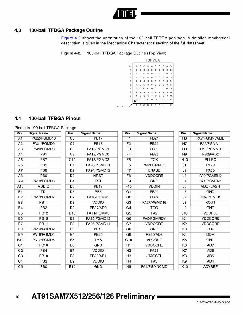
4.3 100-ball TFBGA Package Outline
Figure 4-2 shows the orientation of the 100-ball TFBGA package. A detailed mechanical description is given in the Mechanical Characteristics section of the full datasheet.
Figure 4-2. 100-ball TFBGA Package Outline (Top View)
4.4 100-ball TFBGA Pinout
1
3
4
5
6
7
8
9
10
2
A B C D E F G H J K
TOP VIEW
BALL A1
Pinout in 100-ball TFBGA PackagePin Signal Name Pin Signal Name Pin Signal Name Pin Signal Name
A1 PA22/PGMD10 C6 PB17 F1 PB21 H6 PA7/PGMNVALID
A2 PA21/PGMD9 C7 PB13 F2 PB23 H7 PA9/PGMM1
A3 PA20/PGMD8 C8 PA13/PGMD1 F3 PB25 H8 PA8/PGMM0
A4 PB1 C9 PA12/PGMD0 F4 PB26 H9 PB29/AD2
A5 PB7 C10 PA15/PGMD3 F5 TCK H10 PLLRC
A6 PB5 D1 PA23/PGMD11 F6 PA6/PGMNOE J1 PA29
A7 PB8 D2 PA24/PGMD12 F7 ERASE J2 PA30
A8 PB9 D3 NRST F8 VDDCORE J3 PA0/PGMEN0
A9 PA18/PGMD6 D4 TST F9 GND J4 PA1/PGMEN1
A10 VDDIO D5 PB19 F10 VDDIN J5 VDDFLASH
B1 TDI D6 PB6 G1 PB22 J6 GND
B2 PA19/PGMD7 D7 PA10/PGMM2 G2 PB24 J7 XIN/PGMCK
B3 PB11 D8 VDDIO G3 PA27/PGMD15 J8 XOUT
B4 PB2 D9 PB27/AD0 G4 TDO J9 GND
B5 PB12 D10 PA11/PGMM3 G5 PA2 J10 VDDPLL
B6 PB15 E1 PA25/PGMD13 G6 PA5/PGMRDY K1 VDDCORE
B7 PB14 E2 PA26/PGMD14 G7 VDDCORE K2 VDDCORE
B8 PA14/PGMD2 E3 PB18 G8 GND K3 DDP
B9 PA16/PGMD4 E4 PB20 G9 PB30/AD3 K4 DDM
B10 PA17/PGMD5 E5 TMS G10 VDDOUT K5 GND
C1 PB16 E6 GND H1 VDDCORE K6 AD7
C2 PB4 E7 VDDIO H2 PA28 K7 AD6
C3 PB10 E8 PB28/AD1 H3 JTAGSEL K8 AD5
C4 PB3 E9 VDDIO H4 PA3 K9 AD4
C5 PB0 E10 GND H5 PA4/PGMNCMD K10 ADVREF
106120F–ATARM–03-Oct-06
AT91SAM7X512/256/128 Preliminary
AT91SAM7X512/256/128 Preliminary
5. Power Considerations
5.1 Power Supplies
The AT91SAM7X512/256/128 has six types of power supply pins and integrates a voltage regu-lator, allowing the device to be supplied with only one voltage. The six power supply pin types are:
• VDDIN pin. It powers the voltage regulator and the ADC; voltage ranges from 3.0V to 3.6V, 3.3V nominal. In order to decrease current consumption, if the voltage regulator and the ADC are not used, VDDIN, ADVREF, AD4, AD5, AD6 and AD7 should be connected to GND. In this case, VDDOUT should be left unconnected.
• VDDOUT pin. It is the output of the 1.8V voltage regulator.
• VDDIO pin. It powers the I/O lines; voltage ranges from 3.0V to 3.6V, 3.3V nominal.
• VDDFLASH pin. It powers the USB transceivers and a part of the Flash and is required for the Flash to operate correctly; voltage ranges from 3.0V to 3.6V, 3.3V nominal.
• VDDCORE pins. They power the logic of the device; voltage ranges from 1.65V to 1.95V, 1.8V typical. It can be connected to the VDDOUT pin with decoupling capacitor. VDDCORE is required for the device, including its embedded Flash, to operate correctly.
• VDDPLL pin. It powers the oscillator and the PLL. It can be connected directly to the VDDOUT pin.
No separate ground pins are provided for the different power supplies. Only GND pins are pro-vided and should be connected as shortly as possible to the system ground plane.
5.2 Power Consumption
The AT91SAM7X512/256/128 has a static current of less than 60 µA on VDDCORE at 25°C, including the RC oscillator, the voltage regulator and the power-on reset when the brownout detector is deactivated. Activating the brownout detector adds 28 µA static current.
The dynamic power consumption on VDDCORE is less than 90 mA at full speed when running out of the Flash. Under the same conditions, the power consumption on VDDFLASH does not exceed 10 mA.
5.3 Voltage Regulator
The AT91SAM7X512/256/128 embeds a voltage regulator that is managed by the System Controller.
In Normal Mode, the voltage regulator consumes less than 100 µA static current and draws 100 mA of output current.
The voltage regulator also has a Low-power Mode. In this mode, it consumes less than 25 µA static current and draws 1 mA of output current.
Adequate output supply decoupling is mandatory for VDDOUT to reduce ripple and avoid oscil-lations. The best way to achieve this is to use two capacitors in parallel: one external 470 pF (or 1 nF) NPO capacitor should be connected between VDDOUT and GND as close to the chip as possible. One external 2.2 µF (or 3.3 µF) X7R capacitor should be connected between VDDOUT and GND.
116120F–ATARM–03-Oct-06

Adequate input supply decoupling is mandatory for VDDIN in order to improve startup stability and reduce source voltage drop. The input decoupling capacitor should be placed close to the chip. For example, two capacitors can be used in parallel: 100 nF NPO and 4.7 µF X7R.
5.4 Typical Powering Schematics
The AT91SAM7X512/256/128 supports a 3.3V single supply mode. The internal regulator input connected to the 3.3V source and its output feeds VDDCORE and the VDDPLL. Figure 5-1shows the power schematics to be used for USB bus-powered systems.
Figure 5-1. 3.3V System Single Power Supply Schematic
Power Sourceranges
from 4.5V (USB) to 18V
3.3V
VDDIN
VoltageRegulator
VDDOUT
VDDIODC/DC Converter
VDDCORE
VDDFLASH
VDDPLL
126120F–ATARM–03-Oct-06
AT91SAM7X512/256/128 Preliminary

AT91SAM7X512/256/128 Preliminary
6. I/O Lines Considerations
6.1 JTAG Port Pins
TMS, TDI and TCK are schmitt trigger inputs and are not 5-V tolerant. TMS, TDI and TCK do not integrate a pull-up resistor.
TDO is an output, driven at up to VDDIO, and has no pull-up resistor.
The JTAGSEL pin is used to select the JTAG boundary scan when asserted at a high level. The JTAGSEL pin integrates a permanent pull-down resistor of about 15 kΩ to GND, so that it can be left unconnected for normal operations.
6.2 Test Pin
The TST p in is used fo r manufac tur ing tes t or fas t p rogramming mode o f the AT91SAM7X512/256/128 when asserted high. The TST pin integrates a permanent pull-down resistor of about 15 kΩ to GND, so that it can be left unconnected for normal operations.
To enter fast programming mode, the TST pin and the PA0 and PA1 pins should be tied high and PA2 tied to low.
Driving the TST pin at a high level while PA0 or PA1 is driven at 0 leads to unpredictable results.
6.3 Reset Pin
The NRST pin is bidirectional with an open drain output buffer. It is handled by the on-chip reset controller and can be driven low to provide a reset signal to the external components or asserted low externally to reset the microcontroller. There is no constraint on the length of the reset pulse, and the reset controller can guarantee a minimum pulse length. This allows connection of a sim-ple push-button on the NRST pin as system user reset, and the use of the signal NRST to reset all the components of the system.
The NRST pin integrates a permanent pull-up resistor to VDDIO.
6.4 ERASE Pin
The ERASE pin is used to re-initialize the Flash content and some of its NVM bits. It integrates a permanent pull-down resistor of about 15 kΩ to GND, so that it can be left unconnected for nor-mal operations.
This pin is debounced by the RC oscillator to improve the glitch tolerance. When the pin is tied to high during less than 100 ms, ERASE pin is not taken into account. The pin must be tied high during more than 220 ms to perform the re-initialization of the Flash.
6.5 PIO Controller Lines
All the I/O lines, PA0 to PA30 and PB0 to PB30, are 5V-tolerant and all integrate a programma-ble pull-up resistor. Programming of this pull-up resistor is performed independently for each I/O line through the PIO controllers.
5V-tolerant means that the I/O lines can drive voltage level according to VDDIO, but can be driven with a voltage of up to 5.5V. However, driving an I/O line with a voltage over VDDIO while the programmable pull-up resistor is enabled will create a current path through the pull-up resis-
136120F–ATARM–03-Oct-06
tor from the I/O line to VDDIO. Care should be taken, in particular at reset, as all the I/O lines default to input with pull-up resistor enabled at reset.
6.6 I/O Lines Current Drawing
The PIO lines PA0 to PA3 are high-drive current capable. Each of these I/O lines can drive up to 16 mA permanently.
The remaining I/O lines can draw only 8 mA.
However, the total current drawn by all the I/O lines cannot exceed 200 mA.
146120F–ATARM–03-Oct-06
AT91SAM7X512/256/128 Preliminary

AT91SAM7X512/256/128 Preliminary
7. Processor and Architecture
7.1 ARM7TDMI Processor• RISC processor based on ARMv4T Von Neumann architecture
– Runs at up to 55 MHz, providing 0.9 MIPS/MHz
• Two instruction sets
– ARM high-performance 32-bit instruction set
– Thumb high code density 16-bit instruction set
• Three-stage pipeline architecture
– Instruction Fetch (F)
– Instruction Decode (D)
– Execute (E)
7.2 Debug and Test Features• Integrated embedded in-circuit emulator
– Two watchpoint units
– Test access port accessible through a JTAG protocol
– Debug communication channel
• Debug Unit
– Two-pin UART
– Debug communication channel interrupt handling
– Chip ID Register
• IEEE1149.1 JTAG Boundary-scan on all digital pins
7.3 Memory Controller• Programmable Bus Arbiter
– Handles requests from the ARM7TDMI, the Ethernet MAC and the Peripheral DMA Controller
• Address decoder provides selection signals for
– Three internal 1 Mbyte memory areas
– One 256 Mbyte embedded peripheral area
• Abort Status Registers
– Source, Type and all parameters of the access leading to an abort are saved
– Facilitates debug by detection of bad pointers
• Misalignment Detector
– Alignment checking of all data accesses
– Abort generation in case of misalignment
• Remap Command
– Remaps the SRAM in place of the embedded non-volatile memory
– Allows handling of dynamic exception vectors
156120F–ATARM–03-Oct-06

• Embedded Flash Controller
– Embedded Flash interface, up to three programmable wait states
– Prefetch buffer, buffering and anticipating the 16-bit requests, reducing the required wait states
– Key-protected program, erase and lock/unlock sequencer
– Single command for erasing, programming and locking operations
– Interrupt generation in case of forbidden operation
7.4 Peripheral DMA Controller• Handles data transfer between peripherals and memories
• Thirteen channels
– Two for each USART
– Two for the Debug Unit
– Two for the Serial Synchronous Controller
– Two for each Serial Peripheral Interface
– One for the Analog-to-digital Converter
• Low bus arbitration overhead
– One Master Clock cycle needed for a transfer from memory to peripheral
– Two Master Clock cycles needed for a transfer from peripheral to memory
• Next Pointer management for reducing interrupt latency requirements
166120F–ATARM–03-Oct-06
AT91SAM7X512/256/128 Preliminary

AT91SAM7X512/256/128 Preliminary
8. Memories
8.1 AT91SAM7X512• 512 Kbytes of dual-plane Flash Memory
– 2 contiguous banks of 1024 pages of 256 bytes
– Fast access time, 30 MHz single-cycle access in Worst Case conditions
– Page programming time: 6 ms, including page auto-erase
– Page programming without auto-erase: 3 ms
– Full chip erase time: 15 ms
– 10,000 write cycles, 10-year data retention capability
– 32 lock bits, protecting 32 sectors of 64 pages
– Protection Mode to secure contents of the Flash
• 128 Kbytes of Fast SRAM
– Single-cycle access at full speed
8.2 AT91SAM7X256• 256 Kbytes of Flash Memory
– 1024 pages of 256 bytes
– Fast access time, 30 MHz single-cycle access in Worst Case conditions
– Page programming time: 6 ms, including page auto-erase
– Page programming without auto-erase: 3 ms
– Full chip erase time: 15 ms
– 10,000 write cycles, 10-year data retention capability
– 16 lock bits, each protecting 16 sectors of 64 pages
– Protection Mode to secure contents of the Flash
• 64 Kbytes of Fast SRAM
– Single-cycle access at full speed
8.3 AT91SAM7X128• 128 Kbytes of Flash Memory
– 512 pages of 256 bytes
– Fast access time, 30 MHz single-cycle access in Worst Case conditions
– Page programming time: 6 ms, including page auto-erase
– Page programming without auto-erase: 3 ms
– Full chip erase time: 15 ms
– 10,000 write cycles, 10-year data retention capability
– 8 lock bits, each protecting 8 sectors of 64 pages
– Protection Mode to secure contents of the Flash
• 32 Kbytes of Fast SRAM
– Single-cycle access at full speed
176120F–ATARM–03-Oct-06

Figure 8-1. AT91SAM7X512/256/128 Memory Mapping
0x1000 0000
0x0000 0000
0x0FFF FFFF
0xF000 0000
0xEFFF FFFF
0xFFFF FFFF
256 MBytes
256 MBytes
14 x 256 MBytes3,584 MBytes
0x000F FFF0x0010 0000
0x001F FFF0x0020 0000
0x002F FFF0x0030 0000
0x003F FFF0x0040 0000
0x0000 0000
1 MBytes
1 MBytes
1 MBytes
1 MBytes
252 MBytes
0xFFFA 0000
0xFFFA 3FFF0xFFFA 4000
0xF000 0000
0xFFFB 8000
0xFFFC 0000
0xFFFC 3FFF0xFFFC 4000
0xFFFC 7FFF
0xFFFD 4000
0xFFFD 7FFF
0xFFFD 3FFF
0xFFFD FFFF0xFFFE 0000
0xFFFE 3FFF
0xFFFF EFFF
0xFFFF FFFF
0xFFFF F000
0xFFFE 4000
0xFFFE 80000xFFFE 7FFF
0xFFFB 4000
0xFFFB 7FFF
0xFFF9 FFFF
0xFFFC FFFF
0xFFFD 8000
0xFFFD BFFF
0xFFFC BFFF0xFFFC C000
0xFFFB FFFF
0xFFFB C0000xFFFB BFFF
0xFFFA FFFF0xFFFB 0000
0xFFFB 3FFF
0xFFFD 0000
0xFFFD C000
0xFFFC 8000
16 Kbytes
16 Kbytes
16 Kbytes
16 Kbytes
16 Kbytes
16 Kbytes
16 Kbytes
16 Kbytes
16 Kbytes
16 Kbytes
16 Kbytes
16 Kbytes
0x0FFF FFFF
512 Bytes/128 registers
512 Bytes/128 registers
256 Bytes/64 registers
16 Bytes/4 registers
16 Bytes/4 registers
16 Bytes/4 registers
16 Bytes/4 registers
256 Bytes/64 registers
4 Bytes/1 register
512 Bytes/128 registers
512 Bytes/128 registers
0xFFFF F000
0xFFFF F2000xFFFF F1FF
0xFFFF F3FF
0xFFFF FBFF
0xFFFF FCFF
0xFFFF FEFF
0xFFFF FFFF
0xFFFF F400
0xFFFF FC00
0xFFFF FD0F
0xFFFF FC2F
0xFFFF FC3F
0xFFFF FD4F
0xFFFF FC6F
0xFFFF F5FF0xFFFF F600
0xFFFF F7FF0xFFFF F800
0xFFFF FD00
0xFFFF FF00
0xFFFF FD20
0xFFFF FD30
0xFFFF FD40
0xFFFF FD60
0xFFFF FD70
Internal Memories
Undefined(Abort)
(1) Can be ROM, Flash or SRAMdepending on GPNVM2 and REMAP
Flash before RemapSRAM after Remap
Internal Flash
Internal SRAM
Internal ROM
Reserved
Boot Memory (1)
Address Memory Space
Internal Memory Mapping Note:
TC0, TC1, TC2
USART0
USART1
PWMC
Reserved
Reserved
Reserved
Reserved
Reserved
Reserved
Reserved
CAN
EMAC
Reserved
TWI
SSC
SPI0
SPI1
UDP
ADC
AIC
DBGU
PIOA
Reserved
PMC
MC
WDT
PIT
RTT
RSTC
VREG
PIOB
Peripheral Mapping
System Controller Mapping
Internal Peripherals
Reserved
SYSC
186120F–ATARM–03-Oct-06
AT91SAM7X512/256/128 Preliminary

AT91SAM7X512/256/128 Preliminary
8.4 Memory Mapping
8.4.1 Internal SRAM
• The AT91SAM7X512 embeds a high-speed 128 Kbyte SRAM bank.
• The AT91SAM7X256 embeds a high-speed 64 Kbyte SRAM bank.
• The AT91SAM7X128 embeds a high-speed 32 Kbyte SRAM bank.
After reset and until the Remap Command is performed, the SRAM is only accessible at address 0x0020 0000. After Remap, the SRAM also becomes available at address 0x0.
8.4.2 Internal ROM
The AT91SAM7X512/256/128 embeds an Internal ROM. At any time, the ROM is mapped at address 0x30 0000. The ROM contains the FFPI and the SAM-BA program.
8.4.3 Internal Flash
• The AT91SAM7X512 features two banks (dual plane) of 256 Kbytes of Flash.
• The AT91SAM7X256 features one bank (single plane) of 256 Kbytes of Flash.
• The AT91SAM7X128 features one bank (single plane) of 128 Kbytes of Flash.
At any time, the Flash is mapped to address 0x0010 0000. It is also accessible at address 0x0 after the reset, if GPNVM bit 2 is cleared and before the Remap Command.
A general purpose NVM (GPNVM) bit is used to boot either on the ROM (default) or from the Flash.
This GPNVM bit can be cleared or set respectively through the commands “Clear General-pur-pose NVM Bit” and “Set General-purpose NVM Bit” of the EFC User Interface.
Setting the GPNVM Bit 2 selects the boot from the Flash. Asserting ERASE clears the GPNVM Bit 2 and thus selects the boot from the ROM by default.
Figure 8-2. Internal Memory Mapping with GPNVM Bit 2 = 0 (default)
256M Bytes
ROM Before RemapSRAM After Remap
Undefined Areas(Abort)
0x000F FFFF
0x001F FFFF
0x002F FFFF
0x0FFF FFFF
1 M Bytes
1 M Bytes
1 M Bytes
252 M Bytes
Internal FLASH
Internal SRAM
0x0000 0000
0x0010 0000
0x0020 0000
0x0030 0000
Internal ROM
0x003F FFFF0x0040 0000
1 M Bytes
196120F–ATARM–03-Oct-06

Figure 8-3. Internal Memory Mapping with GPNVM Bit 2 = 1
8.5 Embedded Flash
8.5.1 Flash Overview
• The Flash of the AT91SAM7X512 is organized in two banks (dual plane) of 1024 pages of 256 bytes. The 524,288 bytes are organized in 32-bit words.
• The Flash of the AT91SAM7X256 is organized in 1024 pages of 256 bytes (single plane). It reads as 65,536 32-bit words.
• The Flash of the AT91SAM7X128 is organized in 512 pages of 256 bytes (single plane). It reads as 32,768 32-bit words.
The Flash contains a 256-byte write buffer, accessible through a 32-bit interface.
The Flash benefits from the integration of a power reset cell and from the brownout detector. This prevents code corruption during power supply changes, even in the worst conditions.
When Flash is not used (read or write access), it is automatically placed into standby mode.
8.5.2 Embedded Flash Controller
The Embedded Flash Controller (EFC) manages accesses performed by the masters of the sys-tem. It enables reading the Flash and writing the write buffer. It also contains a User Interface, mapped within the Memory Controller on the APB. The User Interface allows:
• programming of the access parameters of the Flash (number of wait states, timings, etc.)
• starting commands such as full erase, page erase, page program, NVM bit set, NVM bit clear, etc.
• getting the end status of the last command
• getting error status
• programming interrupts on the end of the last commands or on errors
The Embedded Flash Controller also provides a dual 32-bit Prefetch Buffer that optimizes 16-bit access to the Flash. This is particularly efficient when the processor is running in Thumb mode.
Two EFCs are embedded in the AT91SAM7X512 to control each bank of 256 KBytes. Dual-plane organization allows concurrent read and program functionality. Read from one memory
256M Bytes
Flash Before RemapSRAM After Remap
Undefined Areas(Abort)
0x000F FFFF
0x001F FFFF
0x002F FFFF
0x0FFF FFFF
1 M Bytes
1 M Bytes
1 M Bytes
252 M Bytes
Internal FLASH
Internal SRAM
0x0000 0000
0x0010 0000
0x0020 0000
0x0030 0000
Internal ROM
0x003F FFFF0x0040 0000
1 M Bytes
206120F–ATARM–03-Oct-06
AT91SAM7X512/256/128 Preliminary
AT91SAM7X512/256/128 Preliminary
plane may be performed even while program or erase functions are being executed in the other memory plane.
One EFC is embedded in the AT91SAM7X256/128 to control the single plane of 256/128 KBytes.
8.5.3 Lock Regions
8.5.3.1 AT91SAM7X512
Two Embedded Flash Controllers each manage 16 lock bits to protect 16 regions of the flash against inadvertent flash erasing or programming commands. The AT91SAM7X512 contains 32 lock regions and each lock region contains 64 pages of 256 bytes. Each lock region has a size of 16 Kbytes.
If a locked-region’s erase or program command occurs, the command is aborted and the EFC trigs an interrupt.
The 32 NVM bits are software programmable through both of the EFC User Interfaces. The com-mand “Set Lock Bit” enables the protection. The command “Clear Lock Bit” unlocks the lock region.
Asserting the ERASE pin clears the lock bits, thus unlocking the entire Flash.
8.5.3.2 AT91SAM7X256
The Embedded Flash Controller manages 16 lock bits to protect 16 regions of the flash against inadvertent flash erasing or programming commands. The AT91SAM7X256 contains 16 lock regions and each lock region contains 64 pages of 256 bytes. Each lock region has a size of 16 Kbytes.
If a locked-region’s erase or program command occurs, the command is aborted and the EFC trigs an interrupt.
The 16 NVM bits are software programmable through the EFC User Interface. The command “Set Lock Bit” enables the protection. The command “Clear Lock Bit” unlocks the lock region.
Asserting the ERASE pin clears the lock bits, thus unlocking the entire Flash.
8.5.3.3 AT91SAM7X128
The Embedded Flash Controller manages 8 lock bits to protect 8 regions of the flash against inadvertent flash erasing or programming commands. The AT91SAM7X128 contains 8 lock regions and each lock region contains 64 pages of 256 bytes. Each lock region has a size of 16 Kbytes.
If a locked-region’s erase or program command occurs, the command is aborted and the EFC trigs an interrupt.
The 8 NVM bits are software programmable through the EFC User Interface. The command “Set Lock Bit” enables the protection. The command “Clear Lock Bit” unlocks the lock region.
Asserting the ERASE pin clears the lock bits, thus unlocking the entire Flash.
8.5.4 Security Bit Feature
The AT91SAM7X512/256/128 features a security bit, based on a specific NVM-Bit. When the security is enabled, any access to the Flash, either through the ICE interface or through the Fast
216120F–ATARM–03-Oct-06
Flash Programming Interface, is forbidden. This ensures the confidentiality of the code pro-grammed in the Flash.
This security bit can only be enabled, through the Command “Set Security Bit” of the EFC User Interface. Disabling the security bit can only be achieved by asserting the ERASE pin at 1, and after a full flash erase is performed. When the security bit is deactivated, all accesses to the flash are permitted.
It is important to note that the assertion of the ERASE pin should always be longer than 220 ms.
As the ERASE pin integrates a permanent pull-down, it can be left unconnected during normal operation. However, it is safer to connect it directly to GND for the final application.
8.5.5 Non-volatile Brownout Detector Control
Two general purpose NVM (GPNVM) bits are used for controlling the brownout detector (BOD), so that even after a power loss, the brownout detector operations remain in their state.
These two GPNVM bits can be cleared or set respectively through the commands “Clear Gen-eral-purpose NVM Bit” and “Set General-purpose NVM Bit” of the EFC User Interface.
• GPNVM Bit 0 is used as a brownout detector enable bit. Setting the GPNVM Bit 0 enables the BOD, clearing it disables the BOD. Asserting ERASE clears the GPNVM Bit 0 and thus disables the brownout detector by default.
• The GPNVM Bit 1 is used as a brownout reset enable signal for the reset controller. Setting the GPNVM Bit 1 enables the brownout reset when a brownout is detected, Clearing the GPNVM Bit 1 disables the brownout reset. Asserting ERASE disables the brownout reset by default.
8.5.6 Calibration Bits
Eight NVM bits are used to calibrate the brownout detector and the voltage regulator. These bits are factory configured and cannot be changed by the user. The ERASE pin has no effect on the calibration bits.
8.6 Fast Flash Programming Interface
The Fast Flash Programming Interface allows programming the device through either a serial JTAG interface or through a multiplexed fully-handshaked parallel port. It allows gang-program-ming with market-standard industrial programmers.
The FFPI supports read, page program, page erase, full erase, lock, unlock and protect commands.
The Fast Flash Programming Interface is enabled and the Fast Programming Mode is entered when the TST pin and the PA0 and PA1 pins are all tied high.
8.7 SAM-BA Boot Assistant
The SAM-BA Boot Assistant is a default Boot Program that provides an easy way to program in-situ the on-chip Flash memory.
The SAM-BA Boot Assistant supports serial communication via the DBGU or the USB Device Port.
• Communication via the DBGU supports a wide range of crystals from 3 to 20 MHz via software auto-detection.
226120F–ATARM–03-Oct-06
AT91SAM7X512/256/128 Preliminary
AT91SAM7X512/256/128 Preliminary
• Communication via the USB Device Port is limited to an 18.432 MHz crystal.
The SAM-BA Boot provides an interface with SAM-BA Graphic User Interface (GUI).
The SAM-BA Boot is in ROM and is mapped at address 0x0 when the GPNVM Bit 2 is set to 0.
When GPNVM bit 2 is set to 1, the device boots from the Flash.
When GPNVM bit 2 is set to 0, the device boots from ROM (SAM-BA).
236120F–ATARM–03-Oct-06

9. System ControllerThe System Controller manages all vital blocks of the microcontroller: interrupts, clocks, power, time, debug and reset.
The System Controller peripherals are all mapped to the highest 4 Kbytes of address space, between addresses 0xFFFF F000 and 0xFFFF FFFF.
Figure 9-1 on page 25 shows the System Controller Block Diagram.
Figure 8-1 on page 18 shows the mapping of the User Interface of the System Controller periph-erals. Note that the Memory Controller configuration user interface is also mapped within this address space.
246120F–ATARM–03-Oct-06
AT91SAM7X512/256/128 Preliminary

AT91SAM7X512/256/128 Preliminary
Figure 9-1. System Controller Block Diagram
NRST
SLCK
Advanced Interrupt Controller
Real-Time Timer
Periodic Interval Timer
Reset Controller
PA0-PA30
periph_nreset
System Controller
Watchdog Timer
wdt_faultWDRPROC
PIO Controller
POR
BOD
RCOSC
gpnvm[0]cal
en
Power Management
Controller
OSC
PLL
XIN
XOUT
PLLRC
MAINCK
PLLCK
pit_irq
MCK
proc_nreset
wdt_irq
periph_irq2-3]periph_nreset
periph_clk[2..18]
PCK
MCK
pmc_irq
UDPCK
nirq
nfiq
rtt_irq
EmbeddedPeripherals
periph_clk[2-3]
pck[0-3]
in
out
enable
ARM7TDMI
SLCK
SLCK
irq0-irq1
fiq
irq0-irq1
fiq
periph_irq[4..19]
periph_irq[2..19]
int
int
periph_nreset
periph_clk[4..19]
EmbeddedFlash
flash_poe
jtag_nreset
flash_poe
gpnvm[0..2]
flash_wrdis
flash_wrdis
proc_nreset
periph_nreset
dbgu_txd
dbgu_rxd
pit_irqrtt_irq
dbgu_irqpmc_irq
rstc_irq
wdt_irq
rstc_irqefc_irq
SLCK
gpnvm[1]
Boundary Scan TAP Controller
jtag_nreset
power_on_reset
debug
PCK
debugidle
debug
Memory Controller
MCK
proc_nreset
bod_rst_en
proc_nreset
periph_nreset
periph_nreset
idle
Debug Unit
dbgu_irqMCK
dbgu_rxd
periph_nreset force_ntrst
dbgu_txd
USB DevicePort
UDPCK
periph_nreset
periph_clk[11]
periph_irq[11]
usb_suspend
usb_suspend
Voltage Regulator
standby
Voltage Regulator
ModeController
security_bit
cal
power_on_reset
force_ntrst
cal
PB0-PB30
efc_irq
256120F–ATARM–03-Oct-06
9.1 Reset Controller • Based on one power-on reset cell and one brownout detector
• Status of the last reset, either Power-up Reset, Software Reset, User Reset, Watchdog Reset, Brownout Reset
• Controls the internal resets and the NRST pin output
• Allows to shape a signal on the NRST line, guaranteeing that the length of the pulse meets any requirement.
9.1.1 Brownout Detector and Power-on Reset
The AT91SAM7X512/256/128 embeds one brownout detection circuit and a power-on reset cell. The power-on reset is supplied with and monitors VDDCORE.
Both signals are provided to the Flash to prevent any code corruption during power-up or power-down sequences or if brownouts occur on the power supplies.
The power-on reset cell has a limited-accuracy threshold at around 1.5V. Its output remains low during power-up until VDDCORE goes over this voltage level. This signal goes to the reset con-troller and allows a full re-initialization of the device.
The brownout detector monitors the VDDCORE and VDDFLASH levels during operation by comparing them to a fixed trigger level. It secures system operations in the most difficult environ-ments and prevents code corruption in case of brownout on the VDDCORE or VDDFLASH.
When the brownout detector is enabled and VDDCORE decreases to a value below the trigger level (Vbot18-, defined as Vbot18 - hyst/2), the brownout output is immediately activated.
When VDDCORE increases above the trigger level (Vbot18+, defined as Vbot18 + hyst/2), the reset is released. The brownout detector only detects a drop if the voltage on VDDCORE stays below the threshold voltage for longer than about 1µs.
The VDDCORE threshold voltage has a hysteresis of about 50 mV, to ensure spike free brown-out detection. The typical value of the brownout detector threshold is 1.68V with an accuracy of ± 2% and is factory calibrated.
When the brownout detector is enabled and VDDFLASH decreases to a value below the trigger level (Vbot33-, defined as Vbot33 - hyst/2), the brownout output is immediately activated.
When VDDFLASH increases above the trigger level (Vbot33+, defined as Vbot33 + hyst/2), the reset is released. The brownout detector only detects a drop if the voltage on VDDCORE stays below the threshold voltage for longer than about 1µs.
The VDDFLASH threshold voltage has a hysteresis of about 50 mV, to ensure spike free brown-out detection. The typical value of the brownout detector threshold is 2.80V with an accuracy of ± 3.5% and is factory calibrated.
The brownout detector is low-power, as it consumes less than 28 µA static current. However, it can be deactivated to save its static current. In this case, it consumes less than 1µA. The deac-tivation is configured through the GPNVM bit 0 of the Flash.
266120F–ATARM–03-Oct-06
AT91SAM7X512/256/128 Preliminary

AT91SAM7X512/256/128 Preliminary
9.2 Clock Generator
The Clock Generator embeds one low-power RC Oscillator, one Main Oscillator and one PLL with the following characteristics:
• RC Oscillator ranges between 22 KHz and 42 KHz
• Main Oscillator frequency ranges between 3 and 20 MHz
• Main Oscillator can be bypassed
• PLL output ranges between 80 and 200 MHz
It provides SLCK, MAINCK and PLLCK.
Figure 9-2. Clock Generator Block Diagram
Embedded RC
Oscillator
Main Oscillator
PLL and Divider
Clock Generator
Power Management
Controller
XIN
XOUT
PLLRC
Slow Clock SLCK
Main ClockMAINCK
PLL ClockPLLCK
ControlStatus
276120F–ATARM–03-Oct-06
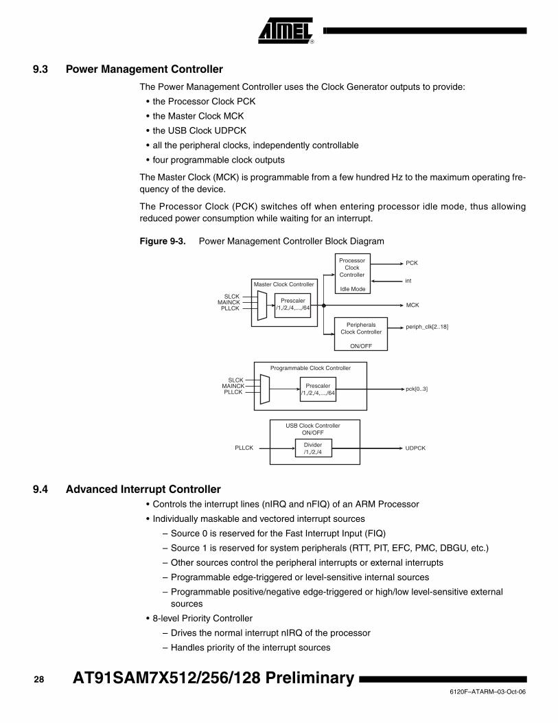
9.3 Power Management Controller
The Power Management Controller uses the Clock Generator outputs to provide:
• the Processor Clock PCK
• the Master Clock MCK
• the USB Clock UDPCK
• all the peripheral clocks, independently controllable
• four programmable clock outputs
The Master Clock (MCK) is programmable from a few hundred Hz to the maximum operating fre-quency of the device.
The Processor Clock (PCK) switches off when entering processor idle mode, thus allowing reduced power consumption while waiting for an interrupt.
Figure 9-3. Power Management Controller Block Diagram
9.4 Advanced Interrupt Controller• Controls the interrupt lines (nIRQ and nFIQ) of an ARM Processor
• Individually maskable and vectored interrupt sources
– Source 0 is reserved for the Fast Interrupt Input (FIQ)
– Source 1 is reserved for system peripherals (RTT, PIT, EFC, PMC, DBGU, etc.)
– Other sources control the peripheral interrupts or external interrupts
– Programmable edge-triggered or level-sensitive internal sources
– Programmable positive/negative edge-triggered or high/low level-sensitive external sources
• 8-level Priority Controller
– Drives the normal interrupt nIRQ of the processor
– Handles priority of the interrupt sources
MCK
periph_clk[2..18]
int
UDPCK
SLCKMAINCK
PLLCKPrescaler
/1,/2,/4,...,/64
PCKProcessor Clock
Controller
Idle ModeMaster Clock Controller
PeripheralsClock Controller
ON/OFF
USB Clock ControllerON/OFF
SLCKMAINCKPLLCK
Prescaler/1,/2,/4,...,/64
Programmable Clock Controller
PLLCK Divider/1,/2,/4
pck[0..3]
286120F–ATARM–03-Oct-06
AT91SAM7X512/256/128 Preliminary

AT91SAM7X512/256/128 Preliminary
– Higher priority interrupts can be served during service of lower priority interrupt
• Vectoring
– Optimizes interrupt service routine branch and execution
– One 32-bit vector register per interrupt source
– Interrupt vector register reads the corresponding current interrupt vector
• Protect Mode
– Easy debugging by preventing automatic operations
• Fast Forcing
– Permits redirecting any interrupt source on the fast interrupt
• General Interrupt Mask
– Provides processor synchronization on events without triggering an interrupt
9.5 Debug Unit• Comprises:
– One two-pin UART
– One Interface for the Debug Communication Channel (DCC) support
– One set of Chip ID Registers
– One Interface providing ICE Access Prevention
• Two-pin UART
– USART-compatible User Interface
– Programmable Baud Rate Generator
– Parity, Framing and Overrun Error
– Automatic Echo, Local Loopback and Remote Loopback Channel Modes
• Debug Communication Channel Support
– Offers visibility of COMMRX and COMMTX signals from the ARM Processor
• Chip ID Registers
– Identification of the device revision, sizes of the embedded memories, set of peripherals
– Chip ID is 0x275C 0A40 (VERSION 0) for AT91SAM7X512
– Chip ID is 0x275B 0940 (VERSION 0) for AT91SAM7X256
– Chip ID is 0x275A 0740 (VERSION 0) for AT91SAM7X128
9.6 Periodic Interval Timer• 20-bit programmable counter plus 12-bit interval counter
9.7 Watchdog Timer• 12-bit key-protected Programmable Counter running on prescaled SLCK
• Provides reset or interrupt signals to the system
• Counter may be stopped while the processor is in debug state or in idle mode
296120F–ATARM–03-Oct-06
9.8 Real-time Timer• 32-bit free-running counter with alarm running on prescaled SLCK
• Programmable 16-bit prescaler for SLCK accuracy compensation
9.9 PIO Controllers• Two PIO Controllers, each controlling 31 I/O lines
• Fully programmable through set/clear registers
• Multiplexing of two peripheral functions per I/O line
• For each I/O line (whether assigned to a peripheral or used as general-purpose I/O)
– Input change interrupt
– Half a clock period glitch filter
– Multi-drive option enables driving in open drain
– Programmable pull-up on each I/O line
– Pin data status register, supplies visibility of the level on the pin at any time
• Synchronous output, provides Set and Clear of several I/O lines in a single write
9.10 Voltage Regulator Controller
The purpose of this controller is to select the Power Mode of the Voltage Regulator between Normal Mode (bit 0 is cleared) or Standby Mode (bit 0 is set).
306120F–ATARM–03-Oct-06
AT91SAM7X512/256/128 Preliminary

AT91SAM7X512/256/128 Preliminary
10. Peripherals
10.1 User Interface
The User Peripherals are mapped in the 256 Mbytes of address space between 0xF000 0000 and 0xFFFF EFFF. Each peripheral is allocated 16 Kbytes of address space.
A complete memory map is provided in Figure 8-1 on page 18.
10.2 Peripheral Identifiers
The AT91SAM7X512/256/128 embeds a wide range of peripherals. Table 10-1 defines the Peripheral Identifiers of the AT91SAM7X512/256/128. Unique peripheral identifiers are defined for both the Advanced Interrupt Controller and the Power Management Controller.
Note: 1. Setting SYSC and ADC bits in the clock set/clear registers of the PMC has no effect. The Sys-tem Controller and ADC are continuously clocked.
Table 10-1. Peripheral Identifiers
Peripheral ID Peripheral Mnemonic Peripheral NameExternal Interrupt
0 AIC Advanced Interrupt Controller FIQ
1 SYSC(1) System Controller
2 PIOA Parallel I/O Controller A
3 PIOB Parallel I/O Controller B
4 SPI0 Serial Peripheral Interface 0
5 SPI1 Serial Peripheral Interface 1
6 US0 USART 0
7 US1 USART 1
8 SSC Synchronous Serial Controller
9 TWI Two-wire Interface
10 PWMC Pulse Width Modulation Controller
11 UDP USB Device Port
12 TC0 Timer/Counter 0
13 TC1 Timer/Counter 1
14 TC2 Timer/Counter 2
15 CAN CAN Controller
16 EMAC Ethernet MAC
17 ADC(1) Analog-to Digital Converter
18 - 29 Reserved
30 AIC Advanced Interrupt Controller IRQ0
31 AIC Advanced Interrupt Controller IRQ1
316120F–ATARM–03-Oct-06

10.3 Peripheral Multiplexing on PIO Lines
The AT91SAM7X512/256/128 features two PIO controllers, PIOA and PIOB, that multiplex the I/O lines of the peripheral set.
Each PIO Controller controls 31 lines. Each line can be assigned to one of two peripheral func-tions, A or B. Some of them can also be multiplexed with the analog inputs of the ADC Controller.
Table 10-2 on page 33 and Table 10-3 on page 34 defines how the I/O lines of the peripherals A, B or the analog inputs are multiplexed on the PIO Controller A and PIO Controller B. The two columns “Function” and “Comments” have been inserted for the user’s own comments; they may be used to track how pins are defined in an application.
Note that some peripheral functions that are output only, may be duplicated in the table.
At reset, all I/O lines are automatically configured as input with the programmable pull-up enabled, so that the device is maintained in a static state as soon as a reset is detected.
326120F–ATARM–03-Oct-06
AT91SAM7X512/256/128 Preliminary
AT91SAM7X512/256/128 Preliminary
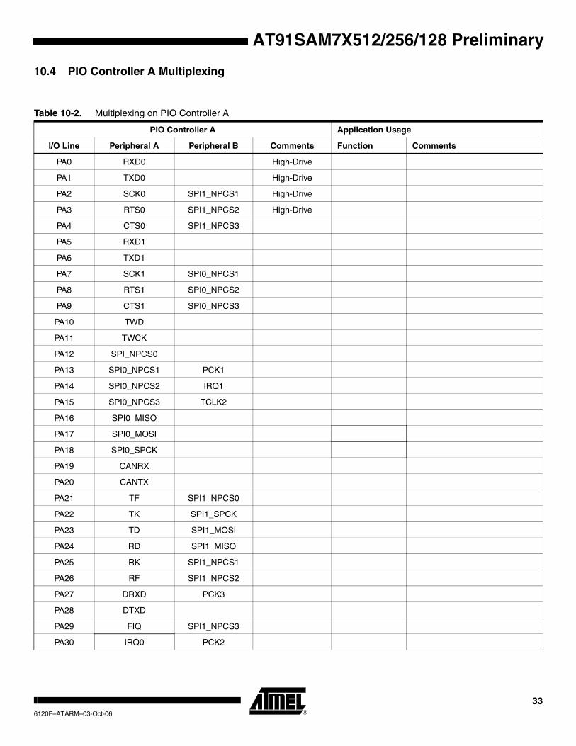
10.4 PIO Controller A Multiplexing
Table 10-2. Multiplexing on PIO Controller A
PIO Controller A Application Usage
I/O Line Peripheral A Peripheral B Comments Function Comments
PA0 RXD0 High-Drive
PA1 TXD0 High-Drive
PA2 SCK0 SPI1_NPCS1 High-Drive
PA3 RTS0 SPI1_NPCS2 High-Drive
PA4 CTS0 SPI1_NPCS3
PA5 RXD1
PA6 TXD1
PA7 SCK1 SPI0_NPCS1
PA8 RTS1 SPI0_NPCS2
PA9 CTS1 SPI0_NPCS3
PA10 TWD
PA11 TWCK
PA12 SPI_NPCS0
PA13 SPI0_NPCS1 PCK1
PA14 SPI0_NPCS2 IRQ1
PA15 SPI0_NPCS3 TCLK2
PA16 SPI0_MISO
PA17 SPI0_MOSI
PA18 SPI0_SPCK
PA19 CANRX
PA20 CANTX
PA21 TF SPI1_NPCS0
PA22 TK SPI1_SPCK
PA23 TD SPI1_MOSI
PA24 RD SPI1_MISO
PA25 RK SPI1_NPCS1
PA26 RF SPI1_NPCS2
PA27 DRXD PCK3
PA28 DTXD
PA29 FIQ SPI1_NPCS3
PA30 IRQ0 PCK2
336120F–ATARM–03-Oct-06

10.5 PIO Controller B Multiplexing
Table 10-3. Multiplexing on PIO Controller B
PIO Controller B Application Usage
I/O Line Peripheral A Peripheral B Comments Function Comments
PB0 ETXCK/EREFCK PCK0
PB1 ETXEN
PB2 ETX0
PB3 ETX1
PB4 ECRS
PB5 ERX0
PB6 ERX1
PB7 ERXER
PB8 EMDC
PB9 EMDIO
PB10 ETX2 SPI1_NPCS1
PB11 ETX3 SPI1_NPCS2
PB12 ETXER TCLK0
PB13 ERX2 SPI0_NPCS1
PB14 ERX3 SPI0_NPCS2
PB15 ERXDV/ECRSDV
PB16 ECOL SPI1_NPCS3
PB17 ERXCK SPI0_NPCS3
PB18 EF100 ADTRG
PB19 PWM0 TCLK1
PB20 PWM1 PCK0
PB21 PWM2 PCK1
PB22 PWM3 PCK2
PB23 TIOA0 DCD1
PB24 TIOB0 DSR1
PB25 TIOA1 DTR1
PB26 TIOB1 RI1
PB27 TIOA2 PWM0 AD0
PB28 TIOB2 PWM1 AD1
PB29 PCK1 PWM2 AD2
PB30 PCK2 PWM3 AD3
346120F–ATARM–03-Oct-06
AT91SAM7X512/256/128 Preliminary

AT91SAM7X512/256/128 Preliminary
10.6 Ethernet MAC• DMA Master on Receive and Transmit Channels
• Compatible with IEEE Standard 802.3
• 10 and 100 Mbit/s operation
• Full- and half-duplex operation
• Statistics Counter Registers
• MII/RMII interface to the physical layer
• Interrupt generation to signal receive and transmit completion
• 28-byte transmit FIFO and 28-byte receive FIFO
• Automatic pad and CRC generation on transmitted frames
• Automatic discard of frames received with errors
• Address checking logic supports up to four specific 48-bit addresses
• Support Promiscuous Mode where all valid received frames are copied to memory
• Hash matching of unicast and multicast destination addresses
• Physical layer management through MDIO interface
• Half-duplex flow control by forcing collisions on incoming frames
• Full-duplex flow control with recognition of incoming pause frames
• Support for 802.1Q VLAN tagging with recognition of incoming VLAN and priority tagged frames
• Multiple buffers per receive and transmit frame
• Jumbo frames up to 10240 bytes supported
10.7 Serial Peripheral Interface• Supports communication with external serial devices
– Four chip selects with external decoder allow communication with up to 15 peripherals
– Serial memories, such as DataFlash® and 3-wire EEPROMs
– Serial peripherals, such as ADCs, DACs, LCD Controllers, CAN Controllers and Sensors
– External co-processors
• Master or slave serial peripheral bus interface
– 8- to 16-bit programmable data length per chip select
– Programmable phase and polarity per chip select
– Programmable transfer delays per chip select, between consecutive transfers and between clock and data
– Programmable delay between consecutive transfers
– Selectable mode fault detection
– Maximum frequency at up to Master Clock
10.8 Two-wire Interface• Master Mode only
• Compatibility with standard two-wire serial memories
356120F–ATARM–03-Oct-06
• One, two or three bytes for slave address
• Sequential read/write operations
10.9 USART• Programmable Baud Rate Generator
• 5- to 9-bit full-duplex synchronous or asynchronous serial communications
– 1, 1.5 or 2 stop bits in Asynchronous Mode
– 1 or 2 stop bits in Synchronous Mode
– Parity generation and error detection
– Framing error detection, overrun error detection
– MSB or LSB first
– Optional break generation and detection
– By 8 or by 16 over-sampling receiver frequency
– Hardware handshaking RTS - CTS
– Modem Signals Management DTR-DSR-DCD-RI on USART1
– Receiver time-out and transmitter timeguard
– Multi-drop Mode with address generation and detection
• RS485 with driver control signal
• ISO7816, T = 0 or T = 1 Protocols for interfacing with smart cards
– NACK handling, error counter with repetition and iteration limit
• IrDA modulation and demodulation
– Communication at up to 115.2 Kbps
• Test Modes
– Remote Loopback, Local Loopback, Automatic Echo
10.10 Serial Synchronous Controller• Provides serial synchronous communication links used in audio and telecom applications
• Contains an independent receiver and transmitter and a common clock divider
• Offers a configurable frame sync and data length
• Receiver and transmitter can be programmed to start automatically or on detection of different event on the frame sync signal
• Receiver and transmitter include a data signal, a clock signal and a frame synchronization signal
10.11 Timer Counter• Three 16-bit Timer Counter Channels
– Three output compare or two input capture
• Wide range of functions including:
– Frequency measurement
– Event counting
– Interval measurement
– Pulse generation
366120F–ATARM–03-Oct-06
AT91SAM7X512/256/128 Preliminary

AT91SAM7X512/256/128 Preliminary
– Delay timing
– Pulse Width Modulation
– Up/down capabilities
• Each channel is user-configurable and contains:
– Three external clock inputs
• Five internal clock inputs, as defined in Table 10-4
– Two multi-purpose input/output signals
– Two global registers that act on all three TC channels
10.12 Pulse Width Modulation Controller• Four channels, one 16-bit counter per channel
• Common clock generator, providing thirteen different clocks
– One Modulo n counter providing eleven clocks
– Two independent linear dividers working on modulo n counter outputs
• Independent channel programming
– Independent enable/disable commands
– Independent clock selection
– Independent period and duty cycle, with double buffering
– Programmable selection of the output waveform polarity
– Programmable center or left aligned output waveform
10.13 USB Device Port• USB V2.0 full-speed compliant,12 Mbits per second
• Embedded USB V2.0 full-speed transceiver
• Embedded 1352-byte dual-port RAM for endpoints
• Six endpoints
– Endpoint 0: 8 bytes
– Endpoint 1 and 2: 64 bytes ping-pong
– Endpoint 3: 64 bytes
– Endpoint 4 and 5: 256 bytes ping-pong
– Ping-pong Mode (two memory banks) for bulk endpoints
• Suspend/resume logic
Table 10-4. Timer Counter Clocks Assignment
TC Clock input Clock
TIMER_CLOCK1 MCK/2
TIMER_CLOCK2 MCK/8
TIMER_CLOCK3 MCK/32
TIMER_CLOCK4 MCK/128
TIMER_CLOCK5 MCK/1024
376120F–ATARM–03-Oct-06

10.14 CAN Controller• Fully compliant with CAN 2.0A and 2.0B
• Bit rates up to 1Mbit/s
• Eight object oriented mailboxes each with the following properties:
– CAN Specification 2.0 Part A or 2.0 Part B Programmable for each Message
– Object configurable to receive (with overwrite or not) or transmit
– Local tag and mask filters up to 29-bit identifier/channel
– 32-bit access to data registers for each mailbox data object
– Uses a 16-bit time stamp on receive and transmit message
– Hardware concatenation of ID unmasked bitfields to speedup family ID processing
– 16-bit internal timer for time stamping and network synchronization
– Programmable reception buffer length up to 8 mailbox objects
– Priority management between transmission mailboxes
– Autobaud and listening mode
– Low power mode and programmable wake-up on bus activity or by the application
– Data, remote, error and overload frame handling
10.15 Analog-to-Digital Converter• 8-channel ADC
• 10-bit 384 K samples/sec. Successive Approximation Register ADC
• -3/+3 LSB Integral Non Linearity, -2/+2 LSB Differential Non Linearity
• Integrated 8-to-1 multiplexer, offering eight independent 3.3V analog inputs
• External voltage reference for better accuracy on low voltage inputs
• Individual enable and disable of each channel
• Multiple trigger sources
– Hardware or software trigger
– External trigger pin
– Timer Counter 0 to 2 outputs TIOA0 to TIOA2 trigger
• Sleep Mode and conversion sequencer
– Automatic wakeup on trigger and back to sleep mode after conversions of all enabled channels
• Four of eight analog inputs shared with digital signals
386120F–ATARM–03-Oct-06
AT91SAM7X512/256/128 Preliminary

AT91SAM7X512/256/128 Preliminary
11. ARM7TDMI Processor Overview
11.1 Overview
The ARM7TDMI core executes both the 32-bit ARM® and 16-bit Thumb® instruction sets, allow-ing the user to trade off between high performance and high code density.The ARM7TDMI processor implements Von Neuman architecture, using a three-stage pipeline consisting of Fetch, Decode, and Execute stages.
The main features of the ARM7tDMI processor are:
• ARM7TDMI Based on ARMv4T Architecture
• Two Instruction Sets
– ARM® High-performance 32-bit Instruction Set
– Thumb® High Code Density 16-bit Instruction Set
• Three-Stage Pipeline Architecture
– Instruction Fetch (F)
– Instruction Decode (D)
– Execute (E)
396120F–ATARM–03-Oct-06
11.2 ARM7TDMI Processor
For further details on ARM7TDMI, refer to the following ARM documents:
ARM Architecture Reference Manual (DDI 0100E)
ARM7TDMI Technical Reference Manual (DDI 0210B)
11.2.1 Instruction Type
Instructions are either 32 bits long (in ARM state) or 16 bits long (in THUMB state).
11.2.2 Data Type
ARM7TDMI supports byte (8-bit), half-word (16-bit) and word (32-bit) data types. Words must be aligned to four-byte boundaries and half words to two-byte boundaries.
Unaligned data access behavior depends on which instruction is used where.
11.2.3 ARM7TDMI Operating Mode
The ARM7TDMI, based on ARM architecture v4T, supports seven processor modes:
User: The normal ARM program execution state
FIQ: Designed to support high-speed data transfer or channel process
IRQ: Used for general-purpose interrupt handling
Supervisor: Protected mode for the operating system
Abort mode: Implements virtual memory and/or memory protection
System: A privileged user mode for the operating system
Undefined: Supports software emulation of hardware coprocessors
Mode changes may be made under software control, or may be brought about by external inter-rupts or exception processing. Most application programs execute in User mode. The non-user modes, or privileged modes, are entered in order to service interrupts or exceptions, or to access protected resources.
11.2.4 ARM7TDMI Registers
The ARM7TDMI processor has a total of 37registers:
• 31 general-purpose 32-bit registers
• 6 status registers
These registers are not accessible at the same time. The processor state and operating mode determine which registers are available to the programmer.
At any one time 16 registers are visible to the user. The remainder are synonyms used to speed up exception processing.
Register 15 is the Program Counter (PC) and can be used in all instructions to reference data relative to the current instruction.
R14 holds the return address after a subroutine call.
R13 is used (by software convention) as a stack pointer.
406120F–ATARM–03-Oct-06
AT91SAM7X512/256/128 Preliminary

AT91SAM7X512/256/128 Preliminary
Registers R0 to R7 are unbanked registers. This means that each of them refers to the same 32-bit physical register in all processor modes. They are general-purpose registers, with no special uses managed by the architecture, and can be used wherever an instruction allows a general-purpose register to be specified.
Registers R8 to R14 are banked registers. This means that each of them depends on the current mode of the processor.
11.2.4.1 Modes and Exception Handling
All exceptions have banked registers for R14 and R13.
After an exception, R14 holds the return address for exception processing. This address is used to return after the exception is processed, as well as to address the instruction that caused the exception.
R13 is banked across exception modes to provide each exception handler with a private stack pointer.
The fast interrupt mode also banks registers 8 to 12 so that interrupt processing can begin with-out having to save these registers.
Table 11-1. ARM7TDMI ARM Modes and Registers Layout
User and System Mode
Supervisor Mode Abort Mode
Undefined Mode
Interrupt Mode
Fast Interrupt Mode
R0 R0 R0 R0 R0 R0
R1 R1 R1 R1 R1 R1
R2 R2 R2 R2 R2 R2
R3 R3 R3 R3 R3 R3
R4 R4 R4 R4 R4 R4
R5 R5 R5 R5 R5 R5
R6 R6 R6 R6 R6 R6
R7 R7 R7 R7 R7 R7
R8 R8 R8 R8 R8 R8_FIQ
R9 R9 R9 R9 R9 R9_FIQ
R10 R10 R10 R10 R10 R10_FIQ
R11 R11 R11 R11 R11 R11_FIQ
R12 R12 R12 R12 R12 R12_FIQ
R13 R13_SVC R13_ABORT R13_UNDEF R13_IRQ R13_FIQ
R14 R14_SVC R14_ABORT R14_UNDEF R14_IRQ R14_FIQ
PC PC PC PC PC PC
CPSR CPSR CPSR CPSR CPSR CPSR
SPSR_SVC SPSR_ABORT SPSR_UNDEF SPSR_IRQ SPSR_FIQ
Mode-specific banked registers
416120F–ATARM–03-Oct-06
A seventh processing mode, System Mode, does not have any banked registers. It uses the User Mode registers. System Mode runs tasks that require a privileged processor mode and allows them to invoke all classes of exceptions.
11.2.4.2 Status Registers
All other processor states are held in status registers. The current operating processor status is in the Current Program Status Register (CPSR). The CPSR holds:
• four ALU flags (Negative, Zero, Carry, and Overflow)
• two interrupt disable bits (one for each type of interrupt)
• one bit to indicate ARM or Thumb execution
• five bits to encode the current processor mode
All five exception modes also have a Saved Program Status Register (SPSR) that holds the CPSR of the task immediately preceding the exception.
11.2.4.3 Exception Types
The ARM7TDMI supports five types of exception and a privileged processing mode for each type. The types of exceptions are:
• fast interrupt (FIQ)
• normal interrupt (IRQ)
• memory aborts (used to implement memory protection or virtual memory)
• attempted execution of an undefined instruction
• software interrupts (SWIs)
Exceptions are generated by internal and external sources.
More than one exception can occur in the same time.
When an exception occurs, the banked version of R14 and the SPSR for the exception mode are used to save state.
To return after handling the exception, the SPSR is moved to the CPSR, and R14 is moved to the PC. This can be done in two ways:
• by using a data-processing instruction with the S-bit set, and the PC as the destination
• by using the Load Multiple with Restore CPSR instruction (LDM)
11.2.5 ARM Instruction Set Overview
The ARM instruction set is divided into:
• Branch instructions
• Data processing instructions
• Status register transfer instructions
• Load and Store instructions
• Coprocessor instructions
• Exception-generating instructions
ARM instructions can be executed conditionally. Every instruction contains a 4-bit condition code field (bit[31:28]).
Table 11-2 gives the ARM instruction mnemonic list.
426120F–ATARM–03-Oct-06
AT91SAM7X512/256/128 Preliminary

AT91SAM7X512/256/128 Preliminary
11.2.6 Thumb Instruction Set Overview
The Thumb instruction set is a re-encoded subset of the ARM instruction set.
The Thumb instruction set is divided into:
• Branch instructions
• Data processing instructions
• Load and Store instructions
• Load and Store Multiple instructions
• Exception-generating instruction
In Thumb mode, eight general-purpose registers, R0 to R7, are available that are the same physical registers as R0 to R7 when executing ARM instructions. Some Thumb instructions also access to the Program Counter (ARM Register 15), the Link Register (ARM Register 14) and the
Table 11-2. ARM Instruction Mnemonic List
Mnemonic Operation Mnemonic Operation
MOV Move CDP Coprocessor Data Processing
ADD Add MVN Move Not
SUB Subtract ADC Add with Carry
RSB Reverse Subtract SBC Subtract with Carry
CMP Compare RSC Reverse Subtract with Carry
TST Test CMN Compare Negated
AND Logical AND TEQ Test Equivalence
EOR Logical Exclusive OR BIC Bit Clear
MUL Multiply ORR Logical (inclusive) OR
SMULL Sign Long Multiply MLA Multiply Accumulate
SMLAL Signed Long Multiply Accumulate UMULL Unsigned Long Multiply
MSR Move to Status Register UMLAL Unsigned Long Multiply Accumulate
B Branch MRS Move From Status Register
BX Branch and Exchange BL Branch and Link
LDR Load Word SWI Software Interrupt
LDRSH Load Signed Halfword STR Store Word
LDRSB Load Signed Byte STRH Store Half Word
LDRH Load Half Word STRB Store Byte
LDRB Load Byte STRBT Store Register Byte with Translation
LDRBT Load Register Byte with Translation STRT Store Register with Translation
LDRT Load Register with Translation STM Store Multiple
LDM Load Multiple SWPB Swap Byte
SWP Swap Word MRC Move From Coprocessor
MCR Move To Coprocessor STC Store From Coprocessor
LDC Load To Coprocessor
436120F–ATARM–03-Oct-06

Stack Pointer (ARM Register 13). Further instructions allow limited access to the ARM registers 8 to 15.
Table 11-3 gives the Thumb instruction mnemonic list.
Table 11-3. Thumb Instruction Mnemonic List
Mnemonic Operation Mnemonic Operation
MOV Move MVN Move Not
ADD Add ADC Add with Carry
SUB Subtract SBC Subtract with Carry
CMP Compare CMN Compare Negated
TST Test NEG Negate
AND Logical AND BIC Bit Clear
EOR Logical Exclusive OR ORR Logical (inclusive) OR
LSL Logical Shift Left LSR Logical Shift Right
ASR Arithmetic Shift Right ROR Rotate Right
MUL Multiply
B Branch BL Branch and Link
BX Branch and Exchange SWI Software Interrupt
LDR Load Word STR Store Word
LDRH Load Half Word STRH Store Half Word
LDRB Load Byte STRB Store Byte
LDRSH Load Signed Halfword LDRSB Load Signed Byte
LDMIA Load Multiple STMIA Store Multiple
PUSH Push Register to stack POP Pop Register from stack
446120F–ATARM–03-Oct-06
AT91SAM7X512/256/128 Preliminary
AT91SAM7X512/256/128 Preliminary
12. Debug and Test Features
12.1 Description
The AT91SAM7X Series features a number of complementary debug and test capabilities. A common JTAG/ICE (In-Circuit Emulator) port is used for standard debugging functions, such as downloading code and single-stepping through programs. The Debug Unit provides a two-pin UART that can be used to upload an application into internal SRAM. It manages the interrupt handling of the internal COMMTX and COMMRX signals that trace the activity of the Debug Communication Channel.
A set of dedicated debug and test input/output pins gives direct access to these capabilities from a PC-based test environment.
12.2 Block Diagram
Figure 12-1. Debug and Test Block Diagram
ICE
PDC DBGU
PIO
DRXD
DTXD
TST
TMS
TCK
TDI
JTAGSEL
TDO
BoundaryTAP
ICE/JTAGTAP
ARM7TDMI
Resetand Test
POR
456120F–ATARM–03-Oct-06
12.3 Application Examples
12.3.1 Debug Environment
Figure 12-2 shows a complete debug environment example. The ICE/JTAG interface is used for standard debugging functions, such as downloading code and single-stepping through the program.
Figure 12-2. Application Debug Environment Example
ICE/JTAGInterface
Host Debugger
ICE/JTAG Connector
TerminalRS232Connector
AT91SAMSxx
AT91SAM7Sxx-based Application Board
466120F–ATARM–03-Oct-06
AT91SAM7X512/256/128 Preliminary

AT91SAM7X512/256/128 Preliminary
12.3.2 Test Environment
Figure 12-3 shows a test environment example. Test vectors are sent and interpreted by the tester. In this example, the “board in test” is designed using a number of JTAG-compliant devices. These devices can be connected to form a single scan chain.
Figure 12-3. Application Test Environment Example
12.4 Debug and Test Pin Description
Tester
JTAG Interface
ICE/JTAG Connector
AT91SAM7Xxx-based Application Board In Test
AT91SAM7Xxx
Test Adaptor
Chip 2Chip n
Chip 1
Table 12-1. Debug and Test Pin List
Pin Name Function Type Active Level
Reset/Test
NRST Microcontroller Reset Input/Output Low
TST Test Mode Select Input High
ICE and JTAG
TCK Test Clock Input
TDI Test Data In Input
TDO Test Data Out Output
TMS Test Mode Select Input
JTAGSEL JTAG Selection Input
Debug Unit
DRXD Debug Receive Data Input
DTXD Debug Transmit Data Output
476120F–ATARM–03-Oct-06

12.5 Functional Description
12.5.1 Test Pin
One dedicated pin, TST, is used to define the device operating mode. The user must make sure that this pin is tied at low level to ensure normal operating conditions. Other values associated with this pin are reserved for manufacturing test.
12.5.2 EmbeddedICE™ (Embedded In-circuit Emulator)
The ARM7TDMI EmbeddedICE is supported via the ICE/JTAG port. The internal state of the ARM7TDMI is examined through an ICE/JTAG port.
The ARM7TDMI processor contains hardware extensions for advanced debugging features:
• In halt mode, a store-multiple (STM) can be inserted into the instruction pipeline. This exports the contents of the ARM7TDMI registers. This data can be serially shifted out without affecting the rest of the system.
• In monitor mode, the JTAG interface is used to transfer data between the debugger and a simple monitor program running on the ARM7TDMI processor.
There are three scan chains inside the ARM7TDMI processor that support testing, debugging, and programming of the EmbeddedICE. The scan chains are controlled by the ICE/JTAG port.
EmbeddedICE mode is selected when JTAGSEL is low. It is not possible to switch directly between ICE and JTAG operations. A chip reset must be performed after JTAGSEL is changed.
For further details on the EmbeddedICE, see the ARM7TDMI (Rev4) Technical Reference Man-ual (DDI0210B).
12.5.3 Debug Unit
The Debug Unit provides a two-pin (DXRD and TXRD) USART that can be used for several debug and trace purposes and offers an ideal means for in-situ programming solutions and debug monitor communication. Moreover, the association with two peripheral data controller channels permits packet handling of these tasks with processor time reduced to a minimum.
The Debug Unit also manages the interrupt handling of the COMMTX and COMMRX signals that come from the ICE and that trace the activity of the Debug Communication Channel. The Debug Unit allows blockage of access to the system through the ICE interface.
A specific register, the Debug Unit Chip ID Register, gives information about the product version and its internal configuration.
The AT91SAM7X512 Debug Unit Chip ID value is 0x275C 0A40 on 32-bit width.
The AT91SAM7X256 Debug Unit Chip ID value is 0x275B 0940 on 32-bit width.
The AT91SAM7X128 Debug Unit Chip ID value is 0x275A 0740 on 32-bit width.
For further details on the Debug Unit, see the Debug Unit section.
12.5.4 IEEE 1149.1 JTAG Boundary Scan
IEEE 1149.1 JTAG Boundary Scan allows pin-level access independent of the device packaging technology.
IEEE 1149.1 JTAG Boundary Scan is enabled when JTAGSEL is high. The SAMPLE, EXTEST and BYPASS functions are implemented. In ICE debug mode, the ARM processor responds
486120F–ATARM–03-Oct-06
AT91SAM7X512/256/128 Preliminary
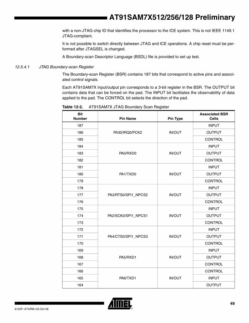
AT91SAM7X512/256/128 Preliminary
with a non-JTAG chip ID that identifies the processor to the ICE system. This is not IEEE 1149.1 JTAG-compliant.
It is not possible to switch directly between JTAG and ICE operations. A chip reset must be per-formed after JTAGSEL is changed.
A Boundary-scan Descriptor Language (BSDL) file is provided to set up test.
12.5.4.1 JTAG Boundary-scan Register
The Boundary-scan Register (BSR) contains 187 bits that correspond to active pins and associ-ated control signals.
Each AT91SAM7X input/output pin corresponds to a 3-bit register in the BSR. The OUTPUT bit contains data that can be forced on the pad. The INPUT bit facilitates the observability of data applied to the pad. The CONTROL bit selects the direction of the pad.
Table 12-2. AT91SAM7X JTAG Boundary Scan Register
Bit Number Pin Name Pin Type
Associated BSR Cells
187
PA30/IRQ0/PCK2 IN/OUT
INPUT
186 OUTPUT
185 CONTROL
184
PA0/RXD0 IN/OUT
INPUT
183 OUTPUT
182 CONTROL
181
PA1/TXD0 IN/OUT
INPUT
180 OUTPUT
179 CONTROL
178
PA3/RTS0/SPI1_NPCS2 IN/OUT
INPUT
177 OUTPUT
176 CONTROL
175
PA2/SCK0/SPI1_NPCS1 IN/OUT
INPUT
174 OUTPUT
173 CONTROL
172
PA4/CTS0/SPI1_NPCS3 IN/OUT
INPUT
171 OUTPUT
170 CONTROL
169
PA5/RXD1 IN/OUT
INPUT
168 OUTPUT
167 CONTROL
166
PA6/TXD1 IN/OUT
CONTROL
165 INPUT
164 OUTPUT
496120F–ATARM–03-Oct-06
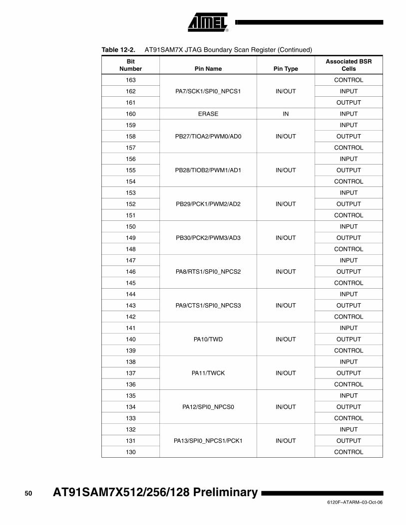
163
PA7/SCK1/SPI0_NPCS1 IN/OUT
CONTROL
162 INPUT
161 OUTPUT
160 ERASE IN INPUT
159
PB27/TIOA2/PWM0/AD0 IN/OUT
INPUT
158 OUTPUT
157 CONTROL
156
PB28/TIOB2/PWM1/AD1 IN/OUT
INPUT
155 OUTPUT
154 CONTROL
153
PB29/PCK1/PWM2/AD2 IN/OUT
INPUT
152 OUTPUT
151 CONTROL
150
PB30/PCK2/PWM3/AD3 IN/OUT
INPUT
149 OUTPUT
148 CONTROL
147
PA8/RTS1/SPI0_NPCS2 IN/OUT
INPUT
146 OUTPUT
145 CONTROL
144
PA9/CTS1/SPI0_NPCS3 IN/OUT
INPUT
143 OUTPUT
142 CONTROL
141
PA10/TWD IN/OUT
INPUT
140 OUTPUT
139 CONTROL
138
PA11/TWCK IN/OUT
INPUT
137 OUTPUT
136 CONTROL
135
PA12/SPI0_NPCS0 IN/OUT
INPUT
134 OUTPUT
133 CONTROL
132
PA13/SPI0_NPCS1/PCK1 IN/OUT
INPUT
131 OUTPUT
130 CONTROL
Table 12-2. AT91SAM7X JTAG Boundary Scan Register (Continued)
Bit Number Pin Name Pin Type
Associated BSR Cells
506120F–ATARM–03-Oct-06
AT91SAM7X512/256/128 Preliminary

AT91SAM7X512/256/128 Preliminary
129
PA14/SPI0_NPCS2/IRQ1 IN/OUT
INPUT
128 OUTPUT
127 CONTROL
126
PA15/SPI0_NPCS3/TCLK2 IN/OUT
INPUT
125 OUTPUT
124 CONTROL
123
PA16/SPI0_MISO IN/OUT
INPUT
122 OUTPUT
121 CONTROL
120
PA17/SPI0_MOSI IN/OUT
INPUT
119 OUTPUT
118 CONTROL
117
PA18/SPI0_SPCK IN/OUT
INPUT
116 OUTPUT
115 CONTROL
114
PB9/EMDIO IN/OUT
INPUT
113 OUTPUT
112 CONTROL
111
PB8/EMDC IN/OUT
INPUT
110 OUTPUT
109 CONTROL
108
PB14/ERX3/SPI0_NPCS2 IN/OUT
INPUT
107 OUTPUT
106 CONTROL
105
PB13/ERX2/SPI0_NPCS1 IN/OUT
INPUT
104 OUTPUT
103 CONTROL
102
PB6/ERX1 IN/OUT
INPUT
101 OUTPUT
100 CONTROL
99
PB5/ERX0 IN/OUT
INPUT
98 OUTPUT
97 CONTROL
Table 12-2. AT91SAM7X JTAG Boundary Scan Register (Continued)
Bit Number Pin Name Pin Type
Associated BSR Cells
516120F–ATARM–03-Oct-06
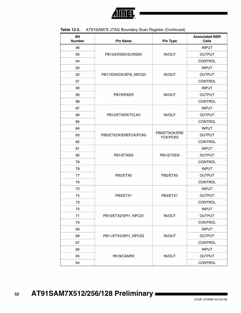
96
PB15/ERXDV/ECRSDV IN/OUT
INPUT
95 OUTPUT
94 CONTROL
93
PB17/ERXCK/SPI0_NPCS3 IN/OUT
INPUT
92 OUTPUT
91 CONTROL
90
PB7/ERXER IN/OUT
INPUT
89 OUTPUT
88 CONTROL
87
PB12/ETXER/TCLK0 IN/OUT
INPUT
86 OUTPUT
85 CONTROL
84
PB0/ETXCK/EREFCK/PCK0PB0/ETXCK/ERE
FCK/PCK0
INPUT
83 OUTPUT
82 CONTROL
81
PB1/ETXEN PB1/ETXEN
INPUT
80 OUTPUT
79 CONTROL
78
PB2/ETX0 PB2/ETX0
INPUT
77 OUTPUT
76 CONTROL
75
PB3/ETX1 PB3/ETX1
INPUT
74 OUTPUT
73 CONTROL
72
PB10/ETX2/SPI1_NPCS1 IN/OUT
INPUT
71 OUTPUT
70 CONTROL
69
PB11/ETX3/SPI1_NPCS2 IN/OUT
INPUT
68 OUTPUT
67 CONTROL
66
PA19/CANRX IN/OUT
INPUT
65 OUTPUT
64 CONTROL
Table 12-2. AT91SAM7X JTAG Boundary Scan Register (Continued)
Bit Number Pin Name Pin Type
Associated BSR Cells
526120F–ATARM–03-Oct-06
AT91SAM7X512/256/128 Preliminary

AT91SAM7X512/256/128 Preliminary
63
PA20/CANTX IN/OUT
INPUT
62 OUTPUT
61 CONTROL
60
PA21/TF/SPI1_NPCS0 IN/OUT
INPUT
59 OUTPUT
58 CONTROL
57
PA22/TK/SPI1_SPCK IN/OUT
INPUT
56 OUTPUT
55 CONTROL
54
PB16/ECOL/SPI1_NPCS3 IN/OUT
INPUT
53 OUTPUT
52 CONTROL
51
PB4/ECRS IN/OUT
INPUT
50 OUTPUT
49 CONTROL
48
PA23/TD/SPI1_MOSI IN/OUT
INPUT
47 OUTPUT
46 CONTROL
45
PA24/RD/SPI1_MISO IN/OUT
INPUT
44 OUTPUT
43 CONTROL
42
PA25/RK/SPI1_NPCS1 IN/OUT
INPUT
41 OUTPUT
40 CONTROL
39
PA26/RF/SPI1_NPCS2 IN/OUT
INPUT
38 OUTPUT
37 CONTROL
36
PB18/EF100/ADTRG IN/OUT
INPUT
35 OUTPUT
34 CONTROL
33
PB19/PWM0/TCLK1 IN/OUT
INPUT
32 OUTPUT
31 CONTROL
Table 12-2. AT91SAM7X JTAG Boundary Scan Register (Continued)
Bit Number Pin Name Pin Type
Associated BSR Cells
536120F–ATARM–03-Oct-06

30
PB20/PWM1/PCK0 IN/OUT
INPUT
29 OUTPUT
28 CONTROL
27
PB21/PWM2/PCK2 IN/OUT
INPUT
26 OUTPUT
25 CONTROL
24
PB22/PWM3/PCK2 IN/OUT
INPUT
23 OUTPUT
22 CONTROL
21
PB23/TIOA0/DCD1 IN/OUT
INPUT
20 OUTPUT
19 CONTROL
18
PB24/TIOB0/DSR1 IN/OUT
INPUT
17 OUTPUT
16 CONTROL
15
PB25/TIOA1/DTR1 IN/OUT
INPUT
14 OUTPUT
13 CONTROL
12
PB26/TIOB1/RI1 IN/OUT
INPUT
11 OUTPUT
10 CONTROL
9
PA27DRXD/PCK3 IN/OUT
INPUT
8 OUTPUT
7 CONTROL
6
PA28/DTXD IN/OUT
INPUT
5 OUTPUT
4 CONTROL
3
PA29/FIQ/SPI1_NPCS3 IN/OUT
INPUT
2 OUTPUT
1 CONTROL
Table 12-2. AT91SAM7X JTAG Boundary Scan Register (Continued)
Bit Number Pin Name Pin Type
Associated BSR Cells
546120F–ATARM–03-Oct-06
AT91SAM7X512/256/128 Preliminary
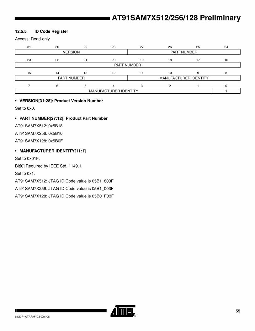
AT91SAM7X512/256/128 Preliminary
12.5.5 ID Code Register
Access: Read-only
• VERSION[31:28]: Product Version Number
Set to 0x0.
• PART NUMBER[27:12]: Product Part Number
AT91SAM7X512: 0x5B18
AT91SAM7X256: 0x5B10
AT91SAM7X128: 0x5B0F
• MANUFACTURER IDENTITY[11:1]
Set to 0x01F.
Bit[0] Required by IEEE Std. 1149.1.
Set to 0x1.
AT91SAM7X512: JTAG ID Code value is 05B1_803F
AT91SAM7X256: JTAG ID Code value is 05B1_003F
AT91SAM7X128: JTAG ID Code value is 05B0_F03F
31 30 29 28 27 26 25 24
VERSION PART NUMBER
23 22 21 20 19 18 17 16
PART NUMBER
15 14 13 12 11 10 9 8
PART NUMBER MANUFACTURER IDENTITY
7 6 5 4 3 2 1 0
MANUFACTURER IDENTITY 1
556120F–ATARM–03-Oct-06

566120F–ATARM–03-Oct-06
AT91SAM7X512/256/128 Preliminary
AT91SAM7X512/256/128 Preliminary
13. Reset Controller (RSTC)
13.1 Overview
The Reset Controller (RSTC), based on power-on reset cells, handles all the resets of the sys-tem without any external components. It reports which reset occurred last.
The Reset Controller also drives independently or simultaneously the external reset and the peripheral and processor resets.
A brownout detection is also available to prevent the processor from falling into an unpredictable state.
13.2 Block Diagram
Figure 13-1. Reset Controller Block Diagram
NRST
StartupCounter
proc_nreset
wd_fault
periph_nreset
SLCK
ResetState
Manager
Reset Controller
brown_out
bod_rst_en
rstc_irq
NRSTManager
exter_nresetnrst_out
Main SupplyPOR
WDRPROC
user_reset
BrownoutManager
bod_reset
576120F–ATARM–03-Oct-06

13.3 Functional Description
The Reset Controller is made up of an NRST Manager, a Brownout Manager, a Startup Counter and a Reset State Manager. It runs at Slow Clock and generates the following reset signals:
• proc_nreset: Processor reset line. It also resets the Watchdog Timer.
• periph_nreset: Affects the whole set of embedded peripherals.
• nrst_out: Drives the NRST pin.
These reset signals are asserted by the Reset Controller, either on external events or on soft-ware action. The Reset State Manager controls the generation of reset signals and provides a signal to the NRST Manager when an assertion of the NRST pin is required.
The NRST Manager shapes the NRST assertion during a programmable time, thus controlling external device resets.
The startup counter waits for the complete crystal oscillator startup. The wait delay is given by the crystal oscillator startup time maximum value that can be found in the section Crystal Oscil-lator Characteristics in the Electrical Characteristics section of the product documentation.
13.3.1 NRST Manager
The NRST Manager samples the NRST input pin and drives this pin low when required by the Reset State Manager. Figure 13-2 shows the block diagram of the NRST Manager.
Figure 13-2. NRST Manager
13.3.1.1 NRST Signal or Interrupt
The NRST Manager samples the NRST pin at Slow Clock speed. When the line is detected low, a User Reset is reported to the Reset State Manager.
However, the NRST Manager can be programmed to not trigger a reset when an assertion of NRST occurs. Writing the bit URSTEN at 0 in RSTC_MR disables the User Reset trigger.
The level of the pin NRST can be read at any time in the bit NRSTL (NRST level) in RSTC_SR. As soon as the pin NRST is asserted, the bit URSTS in RSTC_SR is set. This bit clears only when RSTC_SR is read.
The Reset Controller can also be programmed to generate an interrupt instead of generating a reset. To do so, the bit URSTIEN in RSTC_MR must be written at 1.
External Reset Timer
URSTS
URSTEN
ERSTL
exter_nreset
URSTIEN
RSTC_MR
RSTC_MR
RSTC_MR
RSTC_SR
NRSTL
nrst_out
NRST
rstc_irqOther
interrupt sources
user_reset
586120F–ATARM–03-Oct-06
AT91SAM7X512/256/128 Preliminary

AT91SAM7X512/256/128 Preliminary
13.3.1.2 NRST External Reset Control
The Reset State Manager asserts the signal ext_nreset to assert the NRST pin. When this occurs, the “nrst_out” signal is driven low by the NRST Manager for a time programmed by the field ERSTL in RSTC_MR. This assertion duration, named EXTERNAL_RESET_LENGTH, lasts 2(ERSTL+1) Slow Clock cycles. This gives the approximate duration of an assertion between 60 µs and 2 seconds. Note that ERSTL at 0 defines a two-cycle duration for the NRST pulse.
This feature allows the Reset Controller to shape the NRST pin level, and thus to guarantee that the NRST line is driven low for a time compliant with potential external devices connected on the system reset.
13.3.2 Brownout Manager
Brownout detection prevents the processor from falling into an unpredictable state if the power supply drops below a certain level. When VDDCORE drops below the brownout threshold, the brownout manager requests a brownout reset by asserting the bod_reset signal.
The programmer can disable the brownout reset by setting low the bod_rst_en input signal, i.e.; by locking the corresponding general-purpose NVM bit in the Flash. When the brownout reset is disabled, no reset is performed. Instead, the brownout detection is reported in the bit BODSTS of RSTC_SR. BODSTS is set and clears only when RSTC_SR is read.
The bit BODSTS can trigger an interrupt if the bit BODIEN is set in the RSTC_MR.
At factory, the brownout reset is disabled.
Figure 13-3. Brownout Manager
rstc_irqbrown_out
bod_resetbod_rst_en
BODIEN
RSTC_MR
BODSTS
RSTC_SR
Other interrupt sources
596120F–ATARM–03-Oct-06

13.3.3 Reset States
The Reset State Manager handles the different reset sources and generates the internal reset signals. It reports the reset status in the field RSTTYP of the Status Register (RSTC_SR). The update of the field RSTTYP is performed when the processor reset is released.
13.3.3.1 Power-up Reset
When VDDCORE is powered on, the Main Supply POR cell output is filtered with a start-up counter that operates at Slow Clock. The purpose of this counter is to ensure that the Slow Clock oscillator is stable before starting up the device.
The startup time, as shown in Figure 13-4, is hardcoded to comply with the Slow Clock Oscillator startup time. After the startup time, the reset signals are released and the field RSTTYP in RSTC_SR reports a Power-up Reset.
When VDDCORE is detected low by the Main Supply POR Cell, all reset signals are asserted immediately.
Figure 13-4. Power-up Reset
SLCK
periph_nreset
proc_nreset
Main SupplyPOR output
NRST(nrst_out)
EXTERNAL RESET LENGTH= 2 cycles
Startup Time
MCK
Processor Startup = 3 cycles
AnyFreq.
606120F–ATARM–03-Oct-06
AT91SAM7X512/256/128 Preliminary

AT91SAM7X512/256/128 Preliminary
13.3.3.2 User Reset
The User Reset is entered when a low level is detected on the NRST pin and the bit URSTEN in RSTC_MR is at 1. The NRST input signal is resynchronized with SLCK to insure proper behav-ior of the system.
The User Reset is entered as soon as a low level is detected on NRST. The Processor Reset and the Peripheral Reset are asserted.
The User Reset is left when NRST rises, after a two-cycle resynchronization time and a three-cycle processor startup. The processor clock is re-enabled as soon as NRST is confirmed high.
When the processor reset signal is released, the RSTTYP field of the Status Register (RSTC_SR) is loaded with the value 0x4, indicating a User Reset.
The NRST Manager guaran tees tha t the NRST l i ne i s asse r ted fo r EXTERNAL_RESET_LENGTH Slow Clock cycles, as programmed in the field ERSTL. How-ever, if NRST does not rise after EXTERNAL_RESET_LENGTH because it is driven low externally, the internal reset lines remain asserted until NRST actually rises.
Figure 13-5. User Reset State
SLCK
periph_nreset
proc_nreset
NRST
NRST(nrst_out)
>= EXTERNAL RESET LENGTH
MCK
Processor Startup = 3 cycles
AnyFreq.
Resynch.2 cycles
RSTTYP Any XXX
Resynch.2 cycles
0x4 = User Reset
616120F–ATARM–03-Oct-06
13.3.3.3 Brownout Reset
When the brown_out/bod_reset signal is asserted, the Reset State Manager immediately enters the Brownout Reset. In this state, the processor, the peripheral and the external reset lines are asserted.
The Brownout Reset is left 3 Slow Clock cycles after the rising edge of brown_out/bod_reset after a two-cycle resynchronization. An external reset is also triggered.
When the processor reset is released, the field RSTTYP in RSTC_SR is loaded with the value 0x5, thus indicating that the last reset is a Brownout Reset.
Figure 13-6. Brownout Reset State
SLCK
periph_nreset
proc_nreset
brown_outor bod_reset
NRST(nrst_out)
EXTERNAL RESET LENGTH8 cycles (ERSTL=2)
MCK
Processor Startup = 3 cycles
AnyFreq.
RSTTYP Any XXX 0x5 = Brownout Reset
Resynch.2 cycles
626120F–ATARM–03-Oct-06
AT91SAM7X512/256/128 Preliminary

AT91SAM7X512/256/128 Preliminary
13.3.3.4 Software Reset
The Reset Controller offers several commands used to assert the different reset signals. These commands are performed by writing the Control Register (RSTC_CR) with the following bits at 1:
• PROCRST: Writing PROCRST at 1 resets the processor and the watchdog timer.
• PERRST: Writing PERRST at 1 resets all the embedded peripherals, including the memory system, and, in particular, the Remap Command. The Peripheral Reset is generally used for debug purposes.
• EXTRST: Writing EXTRST at 1 asserts low the NRST pin during a time defined by the field ERSTL in the Mode Register (RSTC_MR).
The software reset is entered if at least one of these bits is set by the software. All these com-mands can be performed independently or simultaneously. The software reset lasts 3 Slow Clock cycles.
The internal reset signals are asserted as soon as the register write is performed. This is detected on the Master Clock (MCK). They are released when the software reset is left, i.e.; syn-chronously to SLCK.
If EXTRST is set, the nrst_out signal is asserted depending on the programming of the field ERSTL. However, the resulting falling edge on NRST does not lead to a User Reset.
If and only if the PROCRST bit is set, the Reset Controller reports the software status in the field RSTTYP of the Status Register (RSTC_SR). Other Software Resets are not reported in RSTTYP.
As soon as a software operation is detected, the bit SRCMP (Software Reset Command in Progress) is set in the Status Register (RSTC_SR). It is cleared as soon as the software reset is left. No other software reset can be performed while the SRCMP bit is set, and writing any value in RSTC_CR has no effect.
Figure 13-7. Software Reset
SLCK
periph_nresetif PERRST=1
proc_nresetif PROCRST=1
Write RSTC_CR
NRST(nrst_out)
if EXTRST=1EXTERNAL RESET LENGTH
8 cycles (ERSTL=2)
MCK
Processor Startup = 3 cycles
AnyFreq.
RSTTYP Any XXX 0x3 = Software Reset
Resynch.1 cycle
SRCMP in RSTC_SR
636120F–ATARM–03-Oct-06
13.3.3.5 Watchdog Reset
The Watchdog Reset is entered when a watchdog fault occurs. This state lasts 3 Slow Clock cycles.
When in Watchdog Reset, assertion of the reset signals depends on the WDRPROC bit in WDT_MR:
• If WDRPROC is 0, the Processor Reset and the Peripheral Reset are asserted. The NRST line is also asserted, depending on the programming of the field ERSTL. However, the resulting low level on NRST does not result in a User Reset state.
• If WDRPROC = 1, only the processor reset is asserted.
The Watchdog Timer is reset by the proc_nreset signal. As the watchdog fault always causes a processor reset if WDRSTEN is set, the Watchdog Timer is always reset after a Watchdog Reset, and the Watchdog is enabled by default and with a period set to a maximum.
When the WDRSTEN in WDT_MR bit is reset, the watchdog fault has no impact on the reset controller.
Figure 13-8. Watchdog Reset
Only if WDRPROC = 0
SLCK
periph_nreset
proc_nreset
wd_fault
NRST(nrst_out)
EXTERNAL RESET LENGTH8 cycles (ERSTL=2)
MCK
Processor Startup = 3 cycles
AnyFreq.
RSTTYP Any XXX 0x2 = Watchdog Reset
646120F–ATARM–03-Oct-06
AT91SAM7X512/256/128 Preliminary

AT91SAM7X512/256/128 Preliminary
13.3.4 Reset State Priorities
The Reset State Manager manages the following priorities between the different reset sources, given in descending order:
• Power-up Reset
• Brownout Reset
• Watchdog Reset
• Software Reset
• User Reset
Particular cases are listed below:
• When in User Reset:
– A watchdog event is impossible because the Watchdog Timer is being reset by the proc_nreset signal.
– A software reset is impossible, since the processor reset is being activated.
• When in Software Reset:
– A watchdog event has priority over the current state.
– The NRST has no effect.
• When in Watchdog Reset:
– The processor reset is active and so a Software Reset cannot be programmed.
– A User Reset cannot be entered.
13.3.5 Reset Controller Status Register
The Reset Controller status register (RSTC_SR) provides several status fields:
• RSTTYP field: This field gives the type of the last reset, as explained in previous sections.
• SRCMP bit: This field indicates that a Software Reset Command is in progress and that no further software reset should be performed until the end of the current one. This bit is automatically cleared at the end of the current software reset.
• NRSTL bit: The NRSTL bit of the Status Register gives the level of the NRST pin sampled on each MCK rising edge.
• URSTS bit: A high-to-low transition of the NRST pin sets the URSTS bit of the RSTC_SR register. This transition is also detected on the Master Clock (MCK) rising edge (see Figure 13-9). If the User Reset is disabled (URSTEN = 0) and if the interruption is enabled by the URSTIEN bit in the RSTC_MR register, the URSTS bit triggers an interrupt. Reading the RSTC_SR status register resets the URSTS bit and clears the interrupt.
• BODSTS bit: This bit indicates a brownout detection when the brownout reset is disabled (bod_rst_en = 0). It triggers an interrupt if the bit BODIEN in the RSTC_MR register enables the interrupt. Reading the RSTC_SR register resets the BODSTS bit and clears the interrupt.
656120F–ATARM–03-Oct-06

Figure 13-9. Reset Controller Status and Interrupt
MCK
NRST
NRSTL
2 cycle resynchronization
2 cycleresynchronization
URSTS
read RSTC_SRPeripheral Access
rstc_irqif (URSTEN = 0) and
(URSTIEN = 1)
666120F–ATARM–03-Oct-06
AT91SAM7X512/256/128 Preliminary

AT91SAM7X512/256/128 Preliminary
13.4 Reset Controller (RSTC) User Interface
Table 13-1. Reset Controller (RSTC) Register Mapping
Offset Register Name Access Reset Value
0x00 Control Register RSTC_CR Write-only -
0x04 Status Register RSTC_SR Read-only 0x0000_0000
0x08 Mode Register RSTC_MR Read/Write 0x0000_0000
676120F–ATARM–03-Oct-06

13.4.1 Reset Controller Control Register
Register Name: RSTC_CR
Access Type: Write-only
• PROCRST: Processor Reset
0 = No effect.
1 = If KEY is correct, resets the processor.
• PERRST: Peripheral Reset
0 = No effect.
1 = If KEY is correct, resets the peripherals.
• EXTRST: External Reset
0 = No effect.
1 = If KEY is correct, asserts the NRST pin.
• KEY: Password
Should be written at value 0xA5. Writing any other value in this field aborts the write operation.
31 30 29 28 27 26 25 24KEY
23 22 21 20 19 18 17 16
– – – – – – – –
15 14 13 12 11 10 9 8
– – – – – – – –
7 6 5 4 3 2 1 0
– – – – EXTRST PERRST – PROCRST
686120F–ATARM–03-Oct-06
AT91SAM7X512/256/128 Preliminary

AT91SAM7X512/256/128 Preliminary
13.4.2 Reset Controller Status Register
Register Name: RSTC_SR
Access Type: Read-only
• URSTS: User Reset Status
0 = No high-to-low edge on NRST happened since the last read of RSTC_SR.
1 = At least one high-to-low transition of NRST has been detected since the last read of RSTC_SR.
• BODSTS: Brownout Detection Status
0 = No brownout high-to-low transition happened since the last read of RSTC_SR.
1 = A brownout high-to-low transition has been detected since the last read of RSTC_SR.
• RSTTYP: Reset Type
Reports the cause of the last processor reset. Reading this RSTC_SR does not reset this field.
• NRSTL: NRST Pin Level
Registers the NRST Pin Level at Master Clock (MCK).
• SRCMP: Software Reset Command in Progress
0 = No software command is being performed by the reset controller. The reset controller is ready for a software command.
1 = A software reset command is being performed by the reset controller. The reset controller is busy.
31 30 29 28 27 26 25 24– – – – – – – –
23 22 21 20 19 18 17 16
– – – – – – SRCMP NRSTL
15 14 13 12 11 10 9 8
– – – – – RSTTYP
7 6 5 4 3 2 1 0
– – – – – – BODSTS URSTS
RSTTYP Reset Type Comments
0 0 0 Power-up Reset VDDCORE rising
0 1 0 Watchdog Reset Watchdog fault occurred
0 1 1 Software Reset Processor reset required by the software
1 0 0 User Reset NRST pin detected low
1 0 1 Brownout Reset BrownOut reset occurred
696120F–ATARM–03-Oct-06

13.4.3 Reset Controller Mode Register
Register Name: RSTC_MR
Access Type: Read/Write
• URSTEN: User Reset Enable
0 = The detection of a low level on the pin NRST does not generate a User Reset.
1 = The detection of a low level on the pin NRST triggers a User Reset.
• URSTIEN: User Reset Interrupt Enable
0 = USRTS bit in RSTC_SR at 1 has no effect on rstc_irq.
1 = USRTS bit in RSTC_SR at 1 asserts rstc_irq if URSTEN = 0.
• BODIEN: Brownout Detection Interrupt Enable
0 = BODSTS bit in RSTC_SR at 1 has no effect on rstc_irq.
1 = BODSTS bit in RSTC_SR at 1 asserts rstc_irq.
• ERSTL: External Reset Length
This field defines the external reset length. The external reset is asserted during a time of 2(ERSTL+1) Slow Clock cycles. This allows assertion duration to be programmed between 60 µs and 2 seconds.
• KEY: Password
Should be written at value 0xA5. Writing any other value in this field aborts the write operation.
31 30 29 28 27 26 25 24KEY
23 22 21 20 19 18 17 16
– – – – – – – BODIEN
15 14 13 12 11 10 9 8
– – – – ERSTL
7 6 5 4 3 2 1 0
– – – URSTIEN – – – URSTEN
706120F–ATARM–03-Oct-06
AT91SAM7X512/256/128 Preliminary

AT91SAM7X512/256/128 Preliminary
14. Real-time Timer (RTT)
14.1 Overview
The Real-time Timer is built around a 32-bit counter and used to count elapsed seconds. It gen-erates a periodic interrupt or/and triggers an alarm on a programmed value.
14.2 Block Diagram
Figure 14-1. Real-time Timer
14.3 Functional Description
The Real-time Timer is used to count elapsed seconds. It is built around a 32-bit counter fed by Slow Clock divided by a programmable 16-bit value. The value can be programmed in the field RTPRES of the Real-time Mode Register (RTT_MR).
Programming RTPRES at 0x00008000 corresponds to feeding the real-time counter with a 1 Hz signal (if the Slow Clock is 32.768 Hz). The 32-bit counter can count up to 232 seconds, corre-sponding to more than 136 years, then roll over to 0.
The Real-time Timer can also be used as a free-running timer with a lower time-base. The best accuracy is achieved by writing RTPRES to 3. Programming RTPRES to 1 or 2 is possible, but may result in losing status events because the status register is cleared two Slow Clock cycles after read. Thus if the RTT is configured to trigger an interrupt, the interrupt occurs during 2 Slow Clock cycles after reading RTT_SR. To prevent several executions of the interrupt handler, the interrupt must be disabled in the interrupt handler and re-enabled when the status register is clear.
SLCK
RTPRES
RTTINC
ALMS
16-bitDivider
32-bitCounter
ALMV
=
CRTV
RTT_MR
RTT_VR
RTT_AR
RTT_SR
RTTINCIEN
RTT_MR
0
1 0
ALMIEN
rtt_int
RTT_MR
set
set
RTT_SR
readRTT_SR
reset
reset
RTT_MR
reload
rtt_alarm
RTTRST
RTT_MR
RTTRST
716120F–ATARM–03-Oct-06
The Real-time Timer value (CRTV) can be read at any time in the register RTT_VR (Real-time Value Register). As this value can be updated asynchronously from the Master Clock, it is advis-able to read this register twice at the same value to improve accuracy of the returned value.
The current value of the counter is compared with the value written in the alarm register RTT_AR (Real-time Alarm Register). If the counter value matches the alarm, the bit ALMS in RTT_SR is set. The alarm register is set to its maximum value, corresponding to 0xFFFF_FFFF, after a reset.
The bit RTTINC in RTT_SR is set each time the Real-time Timer counter is incremented. This bit can be used to start a periodic interrupt, the period being one second when the RTPRES is pro-grammed with 0x8000 and Slow Clock equal to 32.768 Hz.
Reading the RTT_SR status register resets the RTTINC and ALMS fields.
Writing the bit RTTRST in RTT_MR immediately reloads and restarts the clock divider with the new programmed value. This also resets the 32-bit counter.
Note: Because of the asynchronism between the Slow Clock (SCLK) and the System Clock (MCK): 1) The restart of the counter and the reset of the RTT_VR current value register is effective only 2 slow clock cycles after the write of the RTTRST bit in the RTT_MR register. 2) The status register flags reset is taken into account only 2 slow clock cycles after the read of the RTT_SR (Status Register).
Figure 14-2. RTT Counting
Prescaler
ALMVALMV-10 ALMV+1
0
RTPRES - 1
RTT
APB cycle
read RTT_SR
ALMS (RTT_SR)
APB Interface
MCK
RTTINC (RTT_SR)
ALMV+2 ALMV+3...
APB cycle
726120F–ATARM–03-Oct-06
AT91SAM7X512/256/128 Preliminary

AT91SAM7X512/256/128 Preliminary
14.4 Real-time Timer (RTT) User Interface
Table 14-1. Real-time Timer (RTT) Register Mapping
Offset Register Name Access Reset Value
0x00 Mode Register RTT_MR Read/Write 0x0000_8000
0x04 Alarm Register RTT_AR Read/Write 0xFFFF_FFFF
0x08 Value Register RTT_VR Read-only 0x0000_0000
0x0C Status Register RTT_SR Read-only 0x0000_0000
736120F–ATARM–03-Oct-06

14.4.1 Real-time Timer Mode Register
Register Name: RTT_MR
Access Type: Read/Write
• RTPRES: Real-time Timer Prescaler Value
Defines the number of SLCK periods required to increment the real-time timer. RTPRES is defined as follows:
RTPRES = 0: The Prescaler Period is equal to 216
RTPRES ≠ 0: The Prescaler Period is equal to RTPRES.
• ALMIEN: Alarm Interrupt Enable
0 = The bit ALMS in RTT_SR has no effect on interrupt.
1 = The bit ALMS in RTT_SR asserts interrupt.
• RTTINCIEN: Real-time Timer Increment Interrupt Enable
0 = The bit RTTINC in RTT_SR has no effect on interrupt.
1 = The bit RTTINC in RTT_SR asserts interrupt.
• RTTRST: Real-time Timer Restart
1 = Reloads and restarts the clock divider with the new programmed value. This also resets the 32-bit counter.
31 30 29 28 27 26 25 24– – – – – – – –
23 22 21 20 19 18 17 16
– – – – – RTTRST RTTINCIEN ALMIEN
15 14 13 12 11 10 9 8
RTPRES
7 6 5 4 3 2 1 0
RTPRES
746120F–ATARM–03-Oct-06
AT91SAM7X512/256/128 Preliminary
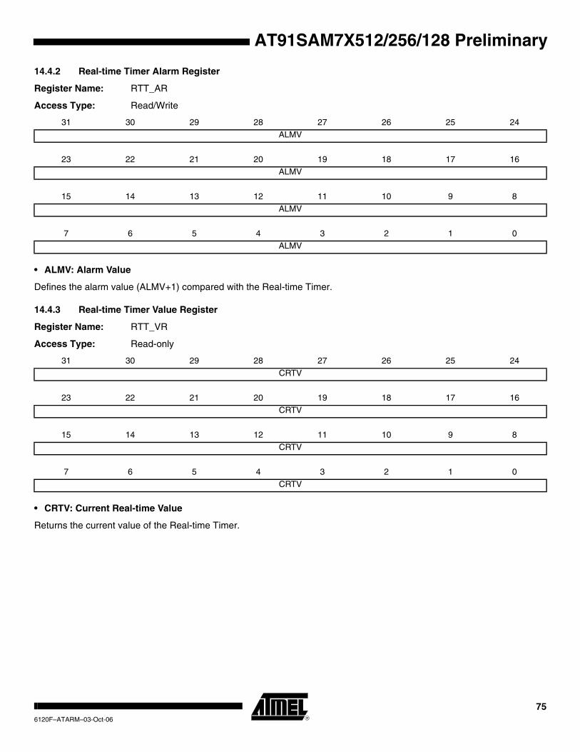
AT91SAM7X512/256/128 Preliminary
14.4.2 Real-time Timer Alarm Register
Register Name: RTT_AR
Access Type: Read/Write
• ALMV: Alarm Value
Defines the alarm value (ALMV+1) compared with the Real-time Timer.
14.4.3 Real-time Timer Value Register
Register Name: RTT_VR
Access Type: Read-only
• CRTV: Current Real-time Value
Returns the current value of the Real-time Timer.
31 30 29 28 27 26 25 24ALMV
23 22 21 20 19 18 17 16
ALMV
15 14 13 12 11 10 9 8
ALMV
7 6 5 4 3 2 1 0
ALMV
31 30 29 28 27 26 25 24
CRTV
23 22 21 20 19 18 17 16
CRTV
15 14 13 12 11 10 9 8
CRTV
7 6 5 4 3 2 1 0
CRTV
756120F–ATARM–03-Oct-06

14.4.4 Real-time Timer Status Register
Register Name: RTT_SR
Access Type: Read-only
• ALMS: Real-time Alarm Status
0 = The Real-time Alarm has not occurred since the last read of RTT_SR.
1 = The Real-time Alarm occurred since the last read of RTT_SR.
• RTTINC: Real-time Timer Increment
0 = The Real-time Timer has not been incremented since the last read of the RTT_SR.
1 = The Real-time Timer has been incremented since the last read of the RTT_SR.
31 30 29 28 27 26 25 24– – – – – – – –
23 22 21 20 19 18 17 16
– – – – – – – –
15 14 13 12 11 10 9 8
– – – – – – – –
7 6 5 4 3 2 1 0
– – – – – – RTTINC ALMS
766120F–ATARM–03-Oct-06
AT91SAM7X512/256/128 Preliminary

AT91SAM7X512/256/128 Preliminary
15. Periodic Interval Timer (PIT)
15.1 Overview
The Periodic Interval Timer (PIT) provides the operating system’s scheduler interrupt. It is designed to offer maximum accuracy and efficient management, even for systems with long response time.
15.2 Block Diagram
Figure 15-1. Periodic Interval Timer
20-bitCounter
MCK/16
PIV
PIT_MR
CPIV PIT_PIVR PICNT
12-bitAdder
0
0
read PIT_PIVR
CPIV PICNTPIT_PIIR
PITSPIT_SR
set
reset
PITIEN
PIT_MR
pit_irq
10
10
MCK
Prescaler
= ?
776120F–ATARM–03-Oct-06

15.3 Functional Description
The Periodic Interval Timer aims at providing periodic interrupts for use by operating systems.
The PIT provides a programmable overflow counter and a reset-on-read feature. It is built around two counters: a 20-bit CPIV counter and a 12-bit PICNT counter. Both counters work at Master Clock /16.
The first 20-bit CPIV counter increments from 0 up to a programmable overflow value set in the field PIV of the Mode Register (PIT_MR). When the counter CPIV reaches this value, it resets to 0 and increments the Periodic Interval Counter, PICNT. The status bit PITS in the Status Regis-ter (PIT_SR) rises and triggers an interrupt, provided the interrupt is enabled (PITIEN in PIT_MR).
Writing a new PIV value in PIT_MR does not reset/restart the counters.
When CPIV and PICNT values are obtained by reading the Periodic Interval Value Register (PIT_PIVR), the overflow counter (PICNT) is reset and the PITS is cleared, thus acknowledging the interrupt. The value of PICNT gives the number of periodic intervals elapsed since the last read of PIT_PIVR.
When CPIV and PICNT values are obtained by reading the Periodic Interval Image Register (PIT_PIIR), there is no effect on the counters CPIV and PICNT, nor on the bit PITS. For exam-ple, a profiler can read PIT_PIIR without clearing any pending interrupt, whereas a timer interrupt clears the interrupt by reading PIT_PIVR.
The PIT may be enabled/disabled using the PITEN bit in the PIT_MR register (disabled on reset). The PITEN bit only becomes effective when the CPIV value is 0. Figure 15-2 illustrates the PIT counting. After the PIT Enable bit is reset (PITEN= 0), the CPIV goes on counting until the PIV value is reached, and is then reset. PIT restarts counting, only if the PITEN is set again.
The PIT is stopped when the core enters debug state.
786120F–ATARM–03-Oct-06
AT91SAM7X512/256/128 Preliminary
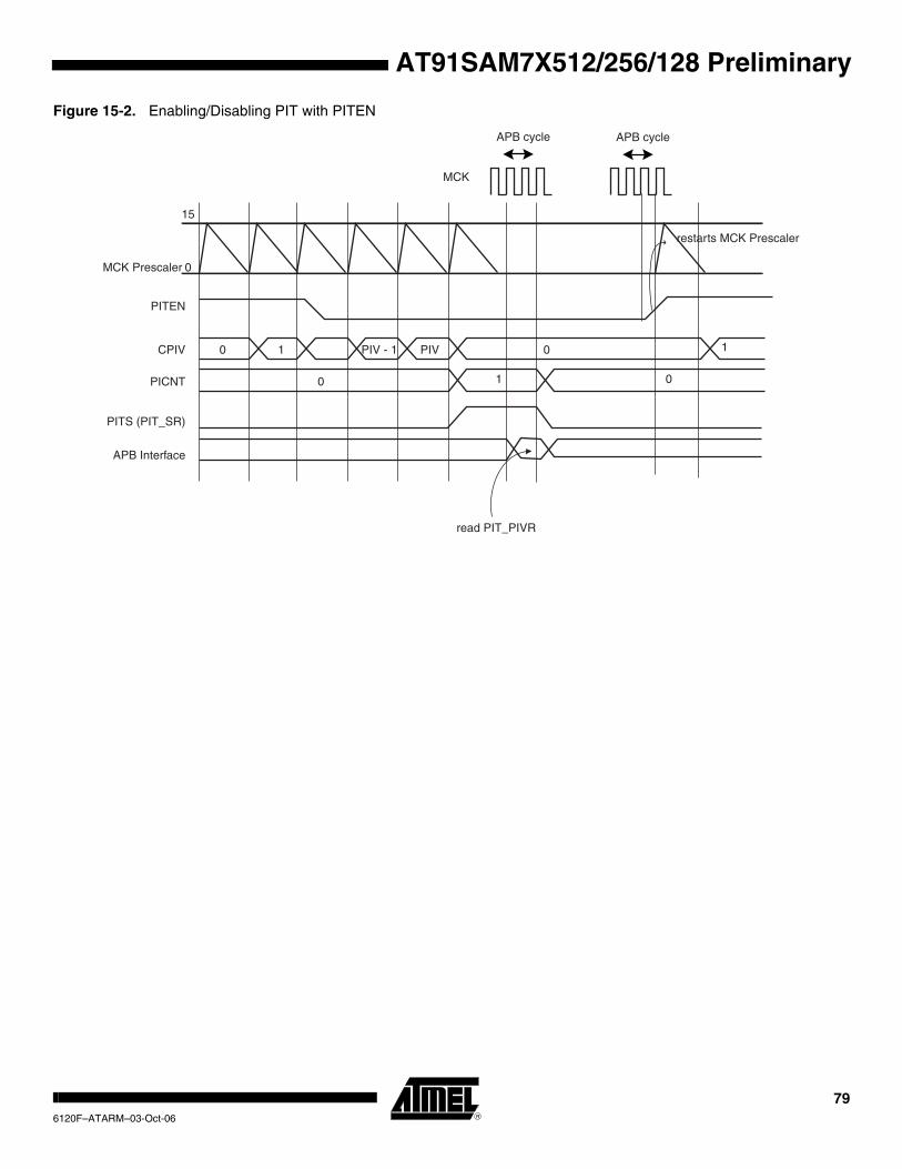
AT91SAM7X512/256/128 Preliminary
Figure 15-2. Enabling/Disabling PIT with PITEN
MCK Prescaler
PIVPIV - 10
PITEN
1 0
0
15
CPIV 1
restarts MCK Prescaler
0 1
APB cycle
read PIT_PIVR
0PICNT
PITS (PIT_SR)
MCK
APB Interface
APB cycle
796120F–ATARM–03-Oct-06
15.4 Periodic Interval Timer (PIT) User Interface
Table 15-1. Periodic Interval Timer (PIT) Register Mapping
Offset Register Name Access Reset Value
0x00 Mode Register PIT_MR Read/Write 0x000F_FFFF
0x04 Status Register PIT_SR Read-only 0x0000_0000
0x08 Periodic Interval Value Register PIT_PIVR Read-only 0x0000_0000
0x0C Periodic Interval Image Register PIT_PIIR Read-only 0x0000_0000
806120F–ATARM–03-Oct-06
AT91SAM7X512/256/128 Preliminary
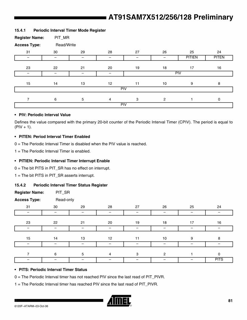
AT91SAM7X512/256/128 Preliminary
15.4.1 Periodic Interval Timer Mode Register
Register Name: PIT_MR
Access Type: Read/Write
• PIV: Periodic Interval Value
Defines the value compared with the primary 20-bit counter of the Periodic Interval Timer (CPIV). The period is equal to (PIV + 1).
• PITEN: Period Interval Timer Enabled
0 = The Periodic Interval Timer is disabled when the PIV value is reached.
1 = The Periodic Interval Timer is enabled.
• PITIEN: Periodic Interval Timer Interrupt Enable
0 = The bit PITS in PIT_SR has no effect on interrupt.
1 = The bit PITS in PIT_SR asserts interrupt.
15.4.2 Periodic Interval Timer Status Register
Register Name: PIT_SR
Access Type: Read-only
• PITS: Periodic Interval Timer Status
0 = The Periodic Interval timer has not reached PIV since the last read of PIT_PIVR.
1 = The Periodic Interval timer has reached PIV since the last read of PIT_PIVR.
31 30 29 28 27 26 25 24– – – – – – PITIEN PITEN
23 22 21 20 19 18 17 16
– – – – PIV
15 14 13 12 11 10 9 8
PIV
7 6 5 4 3 2 1 0
PIV
31 30 29 28 27 26 25 24
– – – – – – – –
23 22 21 20 19 18 17 16
– – – – – – – –
15 14 13 12 11 10 9 8
– – – – – – – –
7 6 5 4 3 2 1 0
– – – – – – – PITS
816120F–ATARM–03-Oct-06

15.4.3 Periodic Interval Timer Value Register
Register Name: PIT_PIVR
Access Type: Read-only
Reading this register clears PITS in PIT_SR.
• CPIV: Current Periodic Interval Value
Returns the current value of the periodic interval timer.
• PICNT: Periodic Interval Counter
Returns the number of occurrences of periodic intervals since the last read of PIT_PIVR.
15.4.4 Periodic Interval Timer Image Register
Register Name: PIT_PIIR
Access Type: Read-only
• CPIV: Current Periodic Interval Value
Returns the current value of the periodic interval timer.
• PICNT: Periodic Interval Counter
Returns the number of occurrences of periodic intervals since the last read of PIT_PIVR.
31 30 29 28 27 26 25 24PICNT
23 22 21 20 19 18 17 16
PICNT CPIV
15 14 13 12 11 10 9 8
CPIV
7 6 5 4 3 2 1 0
CPIV
31 30 29 28 27 26 25 24
PICNT
23 22 21 20 19 18 17 16
PICNT CPIV
15 14 13 12 11 10 9 8
CPIV
7 6 5 4 3 2 1 0
CPIV
826120F–ATARM–03-Oct-06
AT91SAM7X512/256/128 Preliminary
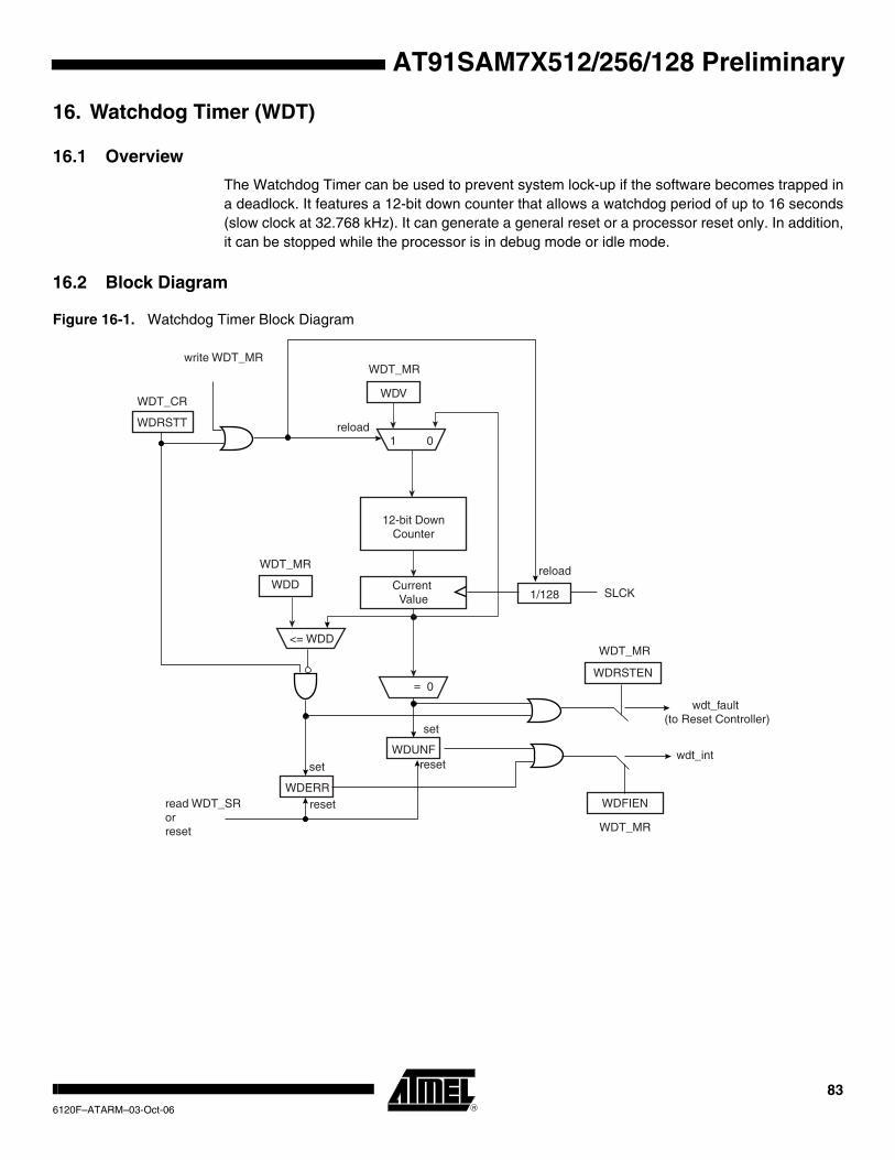
AT91SAM7X512/256/128 Preliminary
16. Watchdog Timer (WDT)
16.1 Overview
The Watchdog Timer can be used to prevent system lock-up if the software becomes trapped in a deadlock. It features a 12-bit down counter that allows a watchdog period of up to 16 seconds (slow clock at 32.768 kHz). It can generate a general reset or a processor reset only. In addition, it can be stopped while the processor is in debug mode or idle mode.
16.2 Block Diagram
Figure 16-1. Watchdog Timer Block Diagram
= 0
1 0
set
resetread WDT_SRorreset
wdt_fault (to Reset Controller)
set
reset
WDFIEN
wdt_int
WDT_MR
SLCK1/128
12-bit DownCounter
Current Value
WDD
WDT_MR
<= WDD
WDV
WDRSTT
WDT_MR
WDT_CR
reload
WDUNF
WDERR
reload
write WDT_MR
WDT_MR
WDRSTEN
836120F–ATARM–03-Oct-06

16.3 Functional Description
The Watchdog Timer can be used to prevent system lock-up if the software becomes trapped in a deadlock. It is supplied with VDDCORE. It restarts with initial values on processor reset.
The Watchdog is built around a 12-bit down counter, which is loaded with the value defined in the field WV of the Mode Register (WDT_MR). The Watchdog Timer uses the Slow Clock divided by 128 to establish the maximum Watchdog period to be 16 seconds (with a typical Slow Clock of 32.768 kHz).
After a Processor Reset, the value of WV is 0xFFF, corresponding to the maximum value of the counter with the external reset generation enabled (field WDRSTEN at 1 after a Backup Reset). This means that a default Watchdog is running at reset, i.e., at power-up. The user must either disable it (by setting the WDDIS bit in WDT_MR) if he does not expect to use it or must repro-gram it to meet the maximum Watchdog period the application requires.
The Watchdog Mode Register (WDT_MR) can be written only once. Only a processor reset resets it. Writing the WDT_MR register reloads the timer with the newly programmed mode parameters.
In normal operation, the user reloads the Watchdog at regular intervals before the timer under-flow occurs, by writing the Control Register (WDT_CR) with the bit WDRSTT to 1. The Watchdog counter is then immediately reloaded from WDT_MR and restarted, and the Slow Clock 128 divider is reset and restarted. The WDT_CR register is write-protected. As a result, writing WDT_CR without the correct hard-coded key has no effect. If an underflow does occur, the “wdt_fault” signal to the Reset Controller is asserted if the bit WDRSTEN is set in the Mode Register (WDT_MR). Moreover, the bit WDUNF is set in the Watchdog Status Register (WDT_SR).
To prevent a software deadlock that continuously triggers the Watchdog, the reload of the Watchdog must occur while the Watchdog counter is within a window between 0 and WDD, WDD is defined in the WatchDog Mode Register WDT_MR.
Any attempt to restart the Watchdog while the Watchdog counter is between WDV and WDD results in a Watchdog error, even if the Watchdog is disabled. The bit WDERR is updated in the WDT_SR and the “wdt_fault” signal to the Reset Controller is asserted.
Note that this feature can be disabled by programming a WDD value greater than or equal to the WDV value. In such a configuration, restarting the Watchdog Timer is permitted in the whole range [0; WDV] and does not generate an error. This is the default configuration on reset (the WDD and WDV values are equal).
The status bits WDUNF (Watchdog Underflow) and WDERR (Watchdog Error) trigger an inter-rupt, provided the bit WDFIEN is set in the mode register. The signal “wdt_fault” to the reset controller causes a Watchdog reset if the WDRSTEN bit is set as already explained in the reset controller programmer Datasheet. In that case, the processor and the Watchdog Timer are reset, and the WDERR and WDUNF flags are reset.
If a reset is generated or if WDT_SR is read, the status bits are reset, the interrupt is cleared, and the “wdt_fault” signal to the reset controller is deasserted.
Writing the WDT_MR reloads and restarts the down counter.
While the processor is in debug state or in idle mode, the counter may be stopped depending on the value programmed for the bits WDIDLEHLT and WDDBGHLT in the WDT_MR.
846120F–ATARM–03-Oct-06
AT91SAM7X512/256/128 Preliminary

AT91SAM7X512/256/128 Preliminary
Figure 16-2. Watchdog Behavior
0
WDV
WDD
WDT_CR = WDRSTTWatchdog
Fault
Normal behavior
Watchdog Error Watchdog Underflow
FFFif WDRSTEN is 1
if WDRSTEN is 0
ForbiddenWindow
PermittedWindow
856120F–ATARM–03-Oct-06

16.4 Watchdog Timer (WDT) User Interface
16.4.1 Watchdog Timer Control Register
Register Name: WDT_CR
Access Type: Write-only
• WDRSTT: Watchdog Restart
0: No effect.
1: Restarts the Watchdog.
• KEY: Password
Should be written at value 0xA5. Writing any other value in this field aborts the write operation.
Table 16-1. Watchdog Timer (WDT) Register Mapping
Offset Register Name Access Reset Value
0x00 Control Register WDT_CR Write-only -
0x04 Mode Register WDT_MR Read/Write Once 0x3FFF_2FFF
0x08 Status Register WDT_SR Read-only 0x0000_0000
31 30 29 28 27 26 25 24KEY
23 22 21 20 19 18 17 16– – – – – – – –
15 14 13 12 11 10 9 8– – – – – – – –
7 6 5 4 3 2 1 0– – – – – – – WDRSTT
866120F–ATARM–03-Oct-06
AT91SAM7X512/256/128 Preliminary

AT91SAM7X512/256/128 Preliminary
16.4.2 Watchdog Timer Mode Register
Register Name: WDT_MR
Access Type: Read/Write Once
• WDV: Watchdog Counter Value
Defines the value loaded in the 12-bit Watchdog Counter.
• WDFIEN: Watchdog Fault Interrupt Enable
0: A Watchdog fault (underflow or error) has no effect on interrupt.
1: A Watchdog fault (underflow or error) asserts interrupt.
• WDRSTEN: Watchdog Reset Enable
0: A Watchdog fault (underflow or error) has no effect on the resets.
1: A Watchdog fault (underflow or error) triggers a Watchdog reset.
• WDRPROC: Watchdog Reset Processor
0: If WDRSTEN is 1, a Watchdog fault (underflow or error) activates all resets.
1: If WDRSTEN is 1, a Watchdog fault (underflow or error) activates the processor reset.
• WDD: Watchdog Delta Value
Defines the permitted range for reloading the Watchdog Timer.
If the Watchdog Timer value is less than or equal to WDD, writing WDT_CR with WDRSTT = 1 restarts the timer.
If the Watchdog Timer value is greater than WDD, writing WDT_CR with WDRSTT = 1 causes a Watchdog error.
• WDDBGHLT: Watchdog Debug Halt
0: The Watchdog runs when the processor is in debug state.
1: The Watchdog stops when the processor is in debug state.
• WDIDLEHLT: Watchdog Idle Halt
0: The Watchdog runs when the system is in idle mode.
1: The Watchdog stops when the system is in idle state.
• WDDIS: Watchdog Disable
0: Enables the Watchdog Timer.
1: Disables the Watchdog Timer.
31 30 29 28 27 26 25 24– – WDIDLEHLT WDDBGHLT WDD
23 22 21 20 19 18 17 16
WDD
15 14 13 12 11 10 9 8
WDDIS WDRPROC WDRSTEN WDFIEN WDV
7 6 5 4 3 2 1 0
WDV
876120F–ATARM–03-Oct-06
16.4.3 Watchdog Timer Status Register
Register Name: WDT_SR
Access Type: Read-only
• WDUNF: Watchdog Underflow
0: No Watchdog underflow occurred since the last read of WDT_SR.
1: At least one Watchdog underflow occurred since the last read of WDT_SR.
• WDERR: Watchdog Error
0: No Watchdog error occurred since the last read of WDT_SR.
1: At least one Watchdog error occurred since the last read of WDT_SR.
31 30 29 28 27 26 25 24– – – – – – – –
23 22 21 20 19 18 17 16
– – – – – – – –
15 14 13 12 11 10 9 8
– – – – – – – –
7 6 5 4 3 2 1 0
– – – – – – WDERR WDUNF
886120F–ATARM–03-Oct-06
AT91SAM7X512/256/128 Preliminary

AT91SAM7X512/256/128 Preliminary
17. Voltage Regulator Mode Controller (VREG)
17.1 Overview
The Voltage Regulator Mode Controller contains one Read/Write register, the Voltage Regulator Mode Register. Its offset is 0x60 with respect to the System Controller offset.
This register controls the Voltage Regulator Mode. Setting PSTDBY (bit 0) puts the Voltage Regulator in Standby Mode or Low-power Mode. On reset, the PSTDBY is reset, so as to wake up the Voltage Regulator in Normal Mode.
896120F–ATARM–03-Oct-06
17.2 Voltage Regulator Power Controller (VREG) User Interface
17.2.1 Voltage Regulator Mode Register
Register Name: VREG_MR
Access Type: Read/Write
• PSTDBY: Periodic Interval Value
0 = Voltage regulator in normal mode.
1 = Voltage regulator in standby mode (low-power mode).
Table 17-1. Voltage Regulator Power Controller Register Mapping
Offset Register Name Access Reset Value
0x60 Voltage Regulator Mode Register VREG_MR Read/Write 0x0
31 30 29 28 27 26 25 24
– – – – – – – –
23 22 21 20 19 18 17 16
– – – – – – – –
15 14 13 12 11 10 9 8
– – – – – – – –
7 6 5 4 3 2 1 0
– – – – – – – PSTDBY
906120F–ATARM–03-Oct-06
AT91SAM7X512/256/128 Preliminary
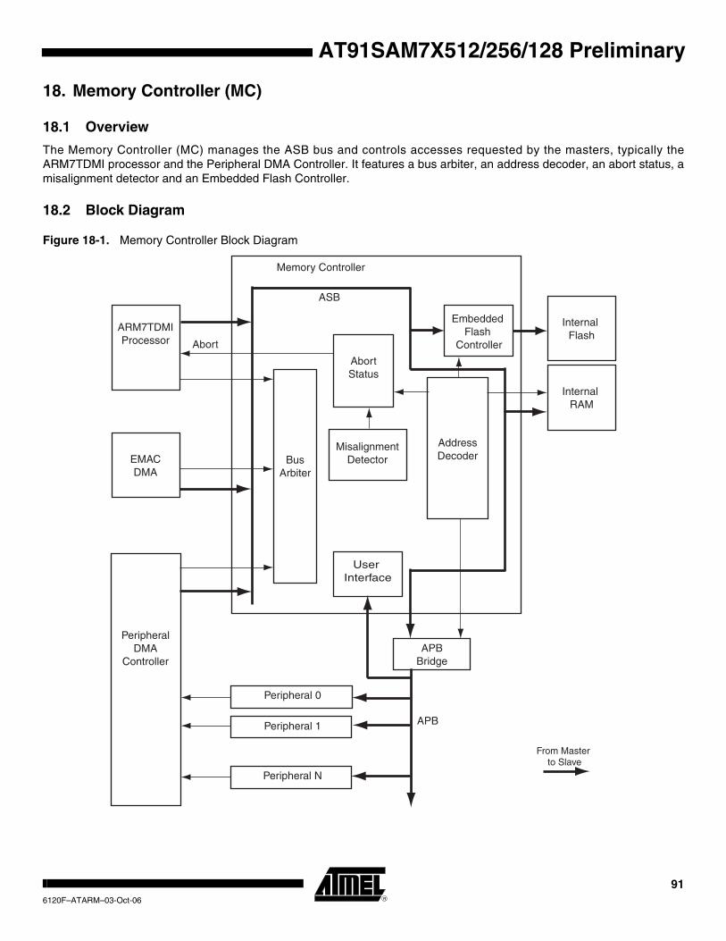
AT91SAM7X512/256/128 Preliminary
18. Memory Controller (MC)
18.1 Overview
The Memory Controller (MC) manages the ASB bus and controls accesses requested by the masters, typically the ARM7TDMI processor and the Peripheral DMA Controller. It features a bus arbiter, an address decoder, an abort status, a misalignment detector and an Embedded Flash Controller.
18.2 Block Diagram
Figure 18-1. Memory Controller Block Diagram
ARM7TDMIProcessor
BusArbiter
PeripheralDMA
Controller
Memory Controller
Abort
ASB
AbortStatus
AddressDecoder
User Interface
Peripheral 0
Peripheral 1
Internal RAM
APB
APBBridge
MisalignmentDetector
From Master to Slave
Peripheral N
Embedded Flash
Controller
Internal Flash
EMACDMA
916120F–ATARM–03-Oct-06

18.3 Functional DescriptionThe Memory Controller handles the internal ASB bus and arbitrates the accesses of up to three masters.
It is made up of:
• A bus arbiter
• An address decoder
• An abort status
• A misalignment detector
• An Embedded Flash Controller
The MC handles only little-endian mode accesses. The masters work in little-endian mode only.
18.3.1 Bus Arbiter
The Memory Controller has a simple, hard-wired priority bus arbiter that gives the control of the bus to one of the three masters. The EMAC has the highest priority; the Peripheral DMA Control-ler has the medium priority; the ARM processor has the lowest one.
18.3.2 Address Decoder
The Memory Controller features an Address Decoder that first decodes the four highest bits of the 32-bit address bus and defines three separate areas:
• One 256-Mbyte address space for the internal memories
• One 256-Mbyte address space reserved for the embedded peripherals
• An undefined address space of 3584M bytes representing fourteen 256-Mbyte areas that return an Abort if accessed
Figure 18-2 shows the assignment of the 256-Mbyte memory areas.
Figure 18-2. Memory Areas
0x0000 0000
0x0FFF FFFF
0x1000 0000
0xEFFF FFFF
0xF000 0000
0xFFFF FFFF
256M Bytes
256M Bytes
14 x 256MBytes3,584 Mbytes
Internal Memories
Undefined(Abort)
Peripherals
926120F–ATARM–03-Oct-06
AT91SAM7X512/256/128 Preliminary

AT91SAM7X512/256/128 Preliminary
18.3.2.1 Internal Memory Mapping
Within the Internal Memory address space, the Address Decoder of the Memory Controller decodes eight more address bits to allocate 1-Mbyte address spaces for the embedded memories.
The allocated memories are accessed all along the 1-Mbyte address space and so are repeated n times within this address space, n equaling 1M bytes divided by the size of the memory.
When the address of the access is undefined within the internal memory area, the Address Decoder returns an Abort to the master.
Figure 18-3. Internal Memory Mapping
18.3.2.2 Internal Memory Area 0
The first 32 bytes of Internal Memory Area 0 contain the ARM processor exception vectors, in particular, the Reset Vector at address 0x0.
Before execution of the remap command, the on-chip Flash is mapped into Internal Memory Area 0, so that the ARM7TDMI reaches an executable instruction contained in Flash. After the remap command, the internal SRAM at address 0x0020 0000 is mapped into Internal Memory Area 0. The memory mapped into Internal Memory Area 0 is accessible in both its original loca-tion and at address 0x0.
18.3.3 Remap Command
After execution, the Remap Command causes the Internal SRAM to be accessed through the Internal Memory Area 0.
As the ARM vectors (Reset, Abort, Data Abort, Prefetch Abort, Undefined Instruction, Interrupt, and Fast Interrupt) are mapped from address 0x0 to address 0x20, the Remap Command allows the user to redefine dynamically these vectors under software control.
The Remap Command is accessible through the Memory Controller User Interface by writing the MC_RCR (Remap Control Register) RCB field to one.
The Remap Command can be cancelled by writing the MC_RCR RCB field to one, which acts as a toggling command. This allows easy debug of the user-defined boot sequence by offering a simple way to put the chip in the same configuration as after a reset.
256M Bytes
Internal Memory Area 0
Undefined Areas(Abort)
0x000F FFFF
0x001F FFFF
0x002F FFFF
0x0FFF FFFF
1 M Bytes
1 M Bytes
1 M Bytes
252 M Bytes
Internal Memory Area 1Internal Flash
Internal Memory Area 2Internal SRAM
0x0000 0000
0x0010 0000
0x0020 0000
0x0030 0000Internal Memory Area 3
Internal ROM0x003F FFFF0x0040 0000
1 M Bytes
936120F–ATARM–03-Oct-06
18.3.4 Abort Status
There are two reasons for an abort to occur:
• access to an undefined address
• an access to a misaligned address.
When an abort occurs, a signal is sent back to all the masters, regardless of which one has gen-erated the access. However, only the ARM7TDMI can take an abort signal into account, and only under the condition that it was generating an access. The Peripheral DMA Controller and the EMAC do not handle the abort input signal. Note that the connections are not represented in Figure 18-1.
To facilitate debug or for fault analysis by an operating system, the Memory Controller integrates an Abort Status register set.
The full 32-bit wide abort address is saved in MC_AASR. Parameters of the access are saved in MC_ASR and include:
• the size of the request (field ABTSZ)
• the type of the access, whether it is a data read or write, or a code fetch (field ABTTYP)
• whether the access is due to accessing an undefined address (bit UNDADD) or a misaligned address (bit MISADD)
• the source of the access leading to the last abort (bits MST_EMAC, MST_PDC and MST_ARM)
• whether or not an abort occurred for each master since the last read of the register (bits SVMST_EMAC, SVMST_PDC and SVMST_ARM) unless this information is loaded in MST bits
In the case of a Data Abort from the processor, the address of the data access is stored. This is useful, as searching for which address generated the abort would require disassembling the instructions and full knowledge of the processor context.
In the case of a Prefetch Abort, the address may have changed, as the prefetch abort is pipe-lined in the ARM processor. The ARM processor takes the prefetch abort into account only if the read instruction is executed and it is probable that several aborts have occurred during this time. Thus, in this case, it is preferable to use the content of the Abort Link register of the ARM processor.
18.3.5 Embedded Flash Controller
The Embedded Flash Controller is added to the Memory Controller and ensures the interface of the flash block with the 32-bit internal bus. It allows an increase of performance in Thumb Mode for Code Fetch with its system of 32-bit buffers. It also manages with the programming, erasing, locking and unlocking sequences thanks to a full set of commands.
18.3.6 Misalignment Detector
The Memory Controller features a Misalignment Detector that checks the consistency of the accesses.
For each access, regardless of the master, the size of the access and the bits 0 and 1 of the address bus are checked. If the type of access is a word (32-bit) and the bits 0 and 1 are not 0, or if the type of the access is a half-word (16-bit) and the bit 0 is not 0, an abort is returned to the master and the access is cancelled. Note that the accesses of the ARM processor when it is fetching instructions are not checked.
The misalignments are generally due to software bugs leading to wrong pointer handling. These bugs are particularly difficult to detect in the debug phase.
946120F–ATARM–03-Oct-06
AT91SAM7X512/256/128 Preliminary

AT91SAM7X512/256/128 Preliminary
As the requested address is saved in the Abort Status Register and the address of the instruc-tion generating the misalignment is saved in the Abort Link Register of the processor, detection and fix of this kind of software bugs is simplified.
956120F–ATARM–03-Oct-06
18.4 Memory Controller (MC) User Interface
Base Address: 0xFFFFFF00
Note: 1. EFC1 pertains to AT91SAM7X512 only.
Table 18-1. Memory Controller (MC) Register Mapping
Offset Register Name Access Reset State
0x00 MC Remap Control Register MC_RCR Write-only
0x04 MC Abort Status Register MC_ASR Read-only 0x0
0x08 MC Abort Address Status Register MC_AASR Read-only 0x0
0x10-0x5C Reserved
0x60 EFC0 Configuration RegistersSee the Embedded Flash Controller Section
0x70 EFC1(1) Configuration Registers
966120F–ATARM–03-Oct-06
AT91SAM7X512/256/128 Preliminary

AT91SAM7X512/256/128 Preliminary
18.4.1 MC Remap Control Register
Register Name: MC_RCR
Access Type: Write-only
Offset: 0x0
• RCB: Remap Command Bit
0: No effect.
1: This Command Bit acts on a toggle basis: writing a 1 alternatively cancels and restores the remapping of the page zero memory devices.
31 30 29 28 27 26 25 24
– – – – – – – –
23 22 21 20 19 18 17 16
– – – – – – – –
15 14 13 12 11 10 9 8
– – – – – – – –
7 6 5 4 3 2 1 0
– – – – – – – RCB
976120F–ATARM–03-Oct-06

18.4.2 MC Abort Status Register
Register Name: MC_ASR
Access Type: Read-only
Reset Value: 0x0
Offset: 0x04
• UNDADD: Undefined Address Abort Status
0: The last abort was not due to the access of an undefined address in the address space.
1: The last abort was due to the access of an undefined address in the address space.
• MISADD: Misaligned Address Abort Status
0: The last aborted access was not due to an address misalignment.
1: The last aborted access was due to an address misalignment.
• ABTSZ: Abort Size Status
• ABTTYP: Abort Type Status
• MST_EMAC: EMAC Abort Source
0: The last aborted access was not due to the EMAC.
1: The last aborted access was due to the EMAC.
31 30 29 28 27 26 25 24
– – – – – SVMST_ARM SVMST_PDC SVMST_EMAC
23 22 21 20 19 18 17 16
– – – – – MST_ARM MST_PDC MST_EMAC
15 14 13 12 11 10 9 8
– – – – ABTTYP ABTSZ
7 6 5 4 3 2 1 0
– – – – – – MISADD UNDADD
ABTSZ Abort Size
0 0 Byte
0 1 Half-word
1 0 Word
1 1 Reserved
ABTTYP Abort Type
0 0 Data Read
0 1 Data Write
1 0 Code Fetch
1 1 Reserved
986120F–ATARM–03-Oct-06
AT91SAM7X512/256/128 Preliminary

AT91SAM7X512/256/128 Preliminary
• MST_PDC: PDC Abort Source
0: The last aborted access was not due to the PDC.
1: The last aborted access was due to the PDC.
• MST_ARM: ARM Abort Source
0: The last aborted access was not due to the ARM.
1: The last aborted access was due to the ARM.
• SVMST_EMAC: Saved EMAC Abort Source
0: No abort due to the EMAC occurred since the last read of MC_ASR or it is notified in the bit MST_EMAC.
1: At least one abort due to the EMAC occurred since the last read of MC_ASR.
• SVMST_PDC: Saved PDC Abort Source
0: No abort due to the PDC occurred since the last read of MC_ASR or it is notified in the bit MST_PDC.
1: At least one abort due to the PDC occurred since the last read of MC_ASR.
• SVMST_ARM: Saved ARM Abort Source
0: No abort due to the ARM occurred since the last read of MC_ASR or it is notified in the bit MST_ARM.
1: At least one abort due to the ARM occurred since the last read of MC_ASR.
996120F–ATARM–03-Oct-06

18.4.3 MC Abort Address Status Register
Register Name: MC_AASR
Access Type: Read-only
Reset Value: 0x0
Offset: 0x08
• ABTADD: Abort Address
This field contains the address of the last aborted access.
31 30 29 28 27 26 25 24
ABTADD
23 22 21 20 19 18 17 16
ABTADD
15 14 13 12 11 10 9 8
ABTADD
7 6 5 4 3 2 1 0
ABTADD
1006120F–ATARM–03-Oct-06
AT91SAM7X512/256/128 Preliminary

AT91SAM7X512/256/128 Preliminary
19. Embedded Flash Controller (EFC)
19.1 Overview
The Embedded Flash Controller (EFC ) is a part of the Memory Controller and ensures the inter-face of the Flash block with the 32-bit internal bus. It increases performance in Thumb Mode for Code Fetch with its system of 32-bit buffers. It also manages the programming, erasing, locking and unlocking sequences using a full set of commands.
The AT91SAM7X512 is equipped with two EFCs, EFC0 and EFC1. EFC1 does not feature the Security bit and GPNVM bits. The Security and GPNVM bits embedded only on EFC0 apply to the two blocks in the AT91SAM7X512.
19.2 Functional Description
19.2.1 Embedded Flash Organization
The Embedded Flash interfaces directly to the 32-bit internal bus. It is composed of several interfaces:
• One memory plane organized in several pages of the same size
• Two 32-bit read buffers used for code read optimization (see ”Read Operations” on page 102).
• One write buffer that manages page programming. The write buffer size is equal to the page size. This buffer is write-only and accessible all along the 1 MByte address space, so that each word can be written to its final address (see ”Write Operations” on page 104).
• Several lock bits used to protect write and erase operations on lock regions. A lock region is composed of several consecutive pages, and each lock region has its associated lock bit.
• Several general-purpose NVM bits. Each bit controls a specific feature in the device. Refer to the product definition section to get the GPNVM assignment.
The Embedded Flash size, the page size and the lock region organization are described in the product definition section.
Table 19-1. Product Specific Lock and General-purpose NVM Bits
AT91SAM7X512 AT91SAM7X256 AT91SAM7X128 Denomination
3 3 3 Number of General-purpose NVM bits
32 16 8 Number of Lock Bits
1016120F–ATARM–03-Oct-06

Figure 19-1. Embedded Flash Memory Mapping
19.2.2 Read Operations
An optimized controller manages embedded Flash reads. A system of 2 x 32-bit buffers is added in order to start access at following address during the second read, thus increasing perfor-mance when the processor is running in Thumb mode (16-bit instruction set). See Figure 19-2, Figure 19-3 and Figure 19-4.
This optimization concerns only Code Fetch and not Data.
The read operations can be performed with or without wait state. Up to 3 wait states can be pro-grammed in the field FWS (Flash Wait State) in the Flash Mode Register MC_FMR (see ”MC Flash Mode Register” on page 112). Defining FWS to be 0 enables the single-cycle access of the embedded Flash.
The Flash memory is accessible through 8-, 16- and 32-bit reads.
As the Flash block size is smaller than the address space reserved for the internal memory area, the embedded Flash wraps around the address space and appears to be repeated within it.
Lock Region 0
Lock Region (n-1)
Page 0
Page (m-1)Start Address
32-bit wide
Flash Memory
Page ( (n-1)*m )
Page (n*m-1)
Lock Bit 0
Lock Region 1 Lock Bit 1
Lock Bit n-1
1026120F–ATARM–03-Oct-06
AT91SAM7X512/256/128 Preliminary

AT91SAM7X512/256/128 Preliminary
Figure 19-2. Code Read Optimization in Thumb Mode for FWS = 0
Note: When FWS is equal to 0, all accesses are performed in a single-cycle access.
Figure 19-3. Code Read Optimization in Thumb Mode for FWS = 1
Note: When FWS is equal to 1, in case of sequential reads, all the accesses are performed in a single-cycle access (except for the first one).
Flash Access
Buffer (32 bits)
Master Clock
ARM Request (16-bit)Code Fetch
Data To ARM
Bytes 0-3 Bytes 4-7
Bytes 0-3
Bytes 0-1 Bytes 2-3 Bytes 4-5 Bytes 6-7 Bytes 8-9 Bytes 10-11 Bytes 12-13
@Byte 0 @Byte 2 @Byte 4 @Byte 6 @Byte 8 @Byte 10 @Byte 12 @Byte 14 @Byte 16
Bytes 14-15
Bytes 4-7
Bytes 8-11
Bytes 8-11
Bytes 12-15 Bytes 16-19
Bytes 12-15
Flash Access
Buffer (32 bits)
Master Clock
ARM Request (16-bit)Code Fetch
Data To ARM
Bytes 0-3 Bytes 4-7
Bytes 0-3
Bytes 2-3 Bytes 4-5 Bytes 6-7 Bytes 8-9 Bytes 10-11
@Byte 0 @Byte 4 @Byte 6 @Byte 8 @Byte 10 @Byte 12 @Byte 14
Bytes 4-7
Bytes 8-11
Bytes 8-11
Bytes 12-15
1 Wait State Cycle
Bytes 0-1
1 Wait State Cycle 1 Wait State Cycle 1 Wait State Cycle
@Byte 2
Bytes 12-13
1036120F–ATARM–03-Oct-06

Figure 19-4. Code Read Optimization in Thumb Mode for FWS = 3
Note: When FWS is equal to 2 or 3, in case of sequential reads, the first access takes FWS cycles, the second access one cycle, the third access FWS cycles, the fourth access one cycle, etc.
19.2.3 Write Operations
The internal memory area reserved for the embedded Flash can also be written through a write-only latch buffer. Write operations take into account only the 8 lowest address bits and thus wrap around within the internal memory area address space and appear to be repeated 1024 times within it.
Write operations can be prevented by programming the Memory Protection Unit of the product.
Writing 8-bit and 16-bit data is not allowed and may lead to unpredictable data corruption.
Write operations are performed in the number of wait states equal to the number of wait states for read operations + 1, except for FWS = 3 (see ”MC Flash Mode Register” on page 112).
19.2.4 Flash Commands
The EFC offers a command set to manage programming the memory flash, locking and unlock-ing lock sectors, consecutive programming and locking, and full Flash erasing.
Flash Access
Master Clock
Data To ARM 0-1
@Byte 0 @2
Bytes 0-3 Bytes 4-7 Bytes 8-11 Bytes 12-15
Bytes 0-3
2-3 6-7
@4
8-9 10-114-5
@8 @12
Bytes 4-7
3 Wait State Cycles
Buffer (32 bits)
ARM Request (16-bit)Code Fetch
Bytes 8-11
3 Wait State Cycles 3 Wait State Cycles 3 Wait State Cycles
@6 @10
12-13
Table 19-2. Set of Commands
Command Value Mnemonic
Write page 0x01 WP
Set Lock Bit 0x02 SLB
Write Page and Lock 0x03 WPL
Clear Lock Bit 0x04 CLB
Erase all 0x08 EA
Set General-purpose NVM Bit 0x0B SGPB
Clear General-purpose NVM Bit 0x0D CGPB
Set Security Bit 0x0F SSB
1046120F–ATARM–03-Oct-06
AT91SAM7X512/256/128 Preliminary
AT91SAM7X512/256/128 Preliminary
To run one of these commands, the field FCMD of the MC_FCR register has to be written with the command number. As soon as the MC_FCR register is written, the FRDY flag is automati-cally cleared. Once the current command is achieved, then the FRDY flag is automatically set. If an interrupt has been enabled by setting the bit FRDY in MC_FMR, the interrupt line of the Mem-ory Controller is activated.
All the commands are protected by the same keyword, which has to be written in the eight high-est bits of the MC_FCR register.
Writing MC_FCR with data that does not contain the correct key and/or with an invalid command has no effect on the memory plane; however, the PROGE flag is set in the MC_FSR register. This flag is automatically cleared by a read access to the MC_FSR register.
When the current command writes or erases a page in a locked region, the command has no effect on the whole memory plane; however, the LOCKE flag is set in the MC_FSR register. This flag is automatically cleared by a read access to the MC_FSR register.
1056120F–ATARM–03-Oct-06
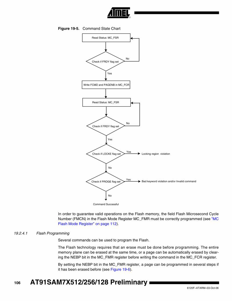
Figure 19-5. Command State Chart
In order to guarantee valid operations on the Flash memory, the field Flash Microsecond Cycle Number (FMCN) in the Flash Mode Register MC_FMR must be correctly programmed (see ”MC Flash Mode Register” on page 112).
19.2.4.1 Flash Programming
Several commands can be used to program the Flash.
The Flash technology requires that an erase must be done before programming. The entire memory plane can be erased at the same time, or a page can be automatically erased by clear-ing the NEBP bit in the MC_FMR register before writing the command in the MC_FCR register.
By setting the NEBP bit in the MC_FMR register, a page can be programmed in several steps if it has been erased before (see Figure 19-6).
Check if FRDY flag setNo
Yes
Read Status: MC_FSR
Write FCMD and PAGENB in MC_FCR
Check if LOCKE flag set
Check if FRDY flag setNo
Read Status: MC_FSR
Yes
YesLocking region violation
No
Check if PROGE flag setYes
No
Bad keyword violation and/or Invalid command
Command Successful
1066120F–ATARM–03-Oct-06
AT91SAM7X512/256/128 Preliminary

AT91SAM7X512/256/128 Preliminary
Figure 19-6. Example of Partial Page Programming:
After programming, the page (the whole lock region) can be locked to prevent miscellaneous write or erase sequences. The lock bit can be automatically set after page programming using WPL.
Data to be written are stored in an internal latch buffer. The size of the latch buffer corresponds to the page size. The latch buffer wraps around within the internal memory area address space and appears to be repeated by the number of pages in it.
Note: Writing of 8-bit and 16-bit data is not allowed and may lead to unpredictable data corruption.
Data are written to the latch buffer before the programming command is written to the Flash Command Register MC_FCR. The sequence is as follows:
• Write the full page, at any page address, within the internal memory area address space using only 32-bit access.
• Programming starts as soon as the page number and the programming command are written to the Flash Command Register. The FRDY bit in the Flash Programming Status Register (MC_FSR) is automatically cleared.
• When programming is completed, the bit FRDY in the Flash Programming Status Register (MC_FSR) rises. If an interrupt was enabled by setting the bit FRDY in MC_FMR, the interrupt line of the Memory Controller is activated.
Two errors can be detected in the MC_FSR register after a programming sequence:
• Programming Error: A bad keyword and/or an invalid command have been written in the MC_FCR register.
• Lock Error: The page to be programmed belongs to a locked region. A command must be previously run to unlock the corresponding region.
19.2.4.2 Erase All Command
The entire memory can be erased if the Erase All Command (EA) in the Flash Command Regis-ter MC_FCR is written.
Erase All Flash Programming of the second part of Page 7 Programming of the third part of Page 7
32 bits wide 32 bits wide 32 bits wide
16 wordsFF FF FF FF
FF FF FF FFFF FF FF FF
FF FF FF FF
FF FF FF FFFF FF FF FF
FF FF FF FF
FF FF FF FFFF FF FF FF
FF FF FF FF
FF FF FF FFFF FF FF FF
...
CA FE CA FE
CA FE CA FECA FE CA FE
FF FF FF FF
FF FF FF FFFF FF FF FF
FF FF FF FF
FF FF FF FFFF FF FF FF
FF FF FF FF
FF FF FF FFFF FF FF FF
CA FE CA FE
CA FE CA FECA FE CA FE
DE CA DE CA
DE CA DE CADE CA DE CA
FF FF FF FF
FF FF FF FFFF FF FF FF
FF FF FF FF
FF FF FF FFFF FF FF FF
Step 1. Step 2. Step 3.
...
...
...
...
...
...
...
...
...
...
...
(NEBP = 1) (NEBP = 1)
16 words
16 words
16 words
Page 7 erased
1076120F–ATARM–03-Oct-06

Erase All operation is allowed only if there are no lock bits set. Thus, if at least one lock region is locked, the bit LOCKE in MC_FSR rises and the command is cancelled. If the bit LOCKE has been written at 1 in MC_FMR, the interrupt line rises.
When programming is complete, the bit FRDY bit in the Flash Programming Status Register (MC_FSR) rises. If an interrupt has been enabled by setting the bit FRDY in MC_FMR, the inter-rupt line of the Memory Controller is activated.
Two errors can be detected in the MC_FSR register after a programming sequence:
• Programming Error: A bad keyword and/or an invalid command have been written in the MC_FCR register.
• Lock Error: At least one lock region to be erased is protected. The erase command has been refused and no page has been erased. A Clear Lock Bit command must be executed previously to unlock the corresponding lock regions.
19.2.4.3 Lock Bit Protection
Lock bits are associated with several pages in the embedded Flash memory plane. This defines lock regions in the embedded Flash memory plane. They prevent writing/erasing protected pages.
After production, the device may have some embedded Flash lock regions locked. These locked regions are reserved for a default application. Refer to the product definition section for the default embedded Flash mapping. Locked sectors can be unlocked to be erased and then pro-grammed with another application or other data.
The lock sequence is:
• The Flash Command register must be written with the following value: (0x5A << 24) | (lockPageNumber << 8 & PAGEN) | SLB lockPageNumber is a page of the corresponding lock region.
• When locking completes, the bit FRDY in the Flash Programming Status Register (MC_FSR) rises. If an interrupt has been enabled by setting the bit FRDY in MC_FMR, the interrupt line of the Memory Controller is activated.
A programming error, where a bad keyword and/or an invalid command have been written in the MC_FCR register, may be detected in the MC_FSR register after a programming sequence.
It is possible to clear lock bits that were set previously. Then the locked region can be erased or programmed. The unlock sequence is:
• The Flash Command register must be written with the following value: (0x5A << 24) | (lockPageNumber << 8 & PAGEN) | CLB lockPageNumber is a page of the corresponding lock region.
• When the unlock completes, the bit FRDY in the Flash Programming Status Register (MC_FSR) rises. If an interrupt has been enabled by setting the bit FRDY in MC_FMR, the interrupt line of the Memory Controller is activated.
A programming error, where a bad keyword and/or an invalid command have been written in the MC_FCR register, may be detected in the MC_FSR register after a programming sequence.
The Unlock command programs the lock bit to 1; the corresponding bit LOCKSx in MC_FSR reads 0. The Lock command programs the lock bit to 0; the corresponding bit LOCKSx in MC_FSR reads 1.
Note: Access to the Flash in Read Mode is permitted when a Lock or Unlock command is performed.
1086120F–ATARM–03-Oct-06
AT91SAM7X512/256/128 Preliminary

AT91SAM7X512/256/128 Preliminary
19.2.4.4 General-purpose NVM Bits
General-purpose NVM bits do not interfere with the embedded Flash memory plane. (Does not apply to EFC1 on the AT91SAM7X512.) These general-purpose bits are dedicated to protect other parts of the product. They can be set (activated) or cleared individually. Refer to the prod-uct definition section for the general-purpose NVM bit action.
The activation sequence is:
• Start the Set General Purpose Bit command (SGPB) by writing the Flash Command Register with the SEL command and the number of the general-purpose bit to be set in the PAGEN field.
• When the bit is set, the bit FRDY in the Flash Programming Status Register (MC_FSR) rises. If an interrupt has been enabled by setting the bit FRDY in MC_FMR, the interrupt line of the Memory Controller is activated.
Two errors can be detected in the MC_FSR register after a programming sequence:
• Programming Error: A bad keyword and/or an invalid command have been written in the MC_FCR register
• If the general-purpose bit number is greater than the total number of general-purpose bits, then the command has no effect.
It is possible to deactivate a general-purpose NVM bit set previously. The clear sequence is:
• Start the Clear General-purpose Bit command (CGPB) by writing the Flash Command Register with CGPB and the number of the general-purpose bit to be cleared in the PAGEN field.
• When the clear completes, the bit FRDY in the Flash Programming Status Register (MC_FSR) rises. If an interrupt has been enabled by setting the bit FRDY in MC_FMR, the interrupt line of the Memory Controller is activated.
Two errors can be detected in the MC_FSR register after a programming sequence:
• Programming Error: a bad keyword and/or an invalid command have been written in the MC_FCR register
• If the number of the general-purpose bit set in the PAGEN field is greater than the total number of general-purpose bits, then the command has no effect.
The Clear General-purpose Bit command programs the general-purpose NVM bit to 1; the corre-sponding bit GPNVM0 to GPNVMx in MC_FSR reads 0. The Set General-purpose Bit command programs the general-purpose NVM bit to 0; the corresponding bit GPNVMx in MC_FSR reads 1.
Note: Access to the Flash in read mode is permitted when a Set, Clear or Get General-purpose NVM Bit command is performed.
19.2.4.5 Security Bit
The goal of the security bit is to prevent external access to the internal bus system. (Does not apply to EFC1 on the AT91SAM7X512.) JTAG, Fast Flash Programming and Flash Serial Test Interface features are disabled. Once set, this bit can be reset only by an external hardware ERASE request to the chip. Refer to the product definition section for the pin name that controls the ERASE. In this case, the full memory plane is erased and all lock and general-purpose NVM bits are cleared. The security bit in the MC_FSR is cleared only after these operations. The acti-vation sequence is:
• Start the Set Security Bit command (SSB) by writing the Flash Command Register.
1096120F–ATARM–03-Oct-06

• When the locking completes, the bit FRDY in the Flash Programming Status Register (MC_FSR) rises. If an interrupt has been enabled by setting the bit FRDY in MC_FMR, the interrupt line of the Memory Controller is activated.
When the security bit is active, the SECURITY bit in the MC_FSR is set.
1106120F–ATARM–03-Oct-06
AT91SAM7X512/256/128 Preliminary

AT91SAM7X512/256/128 Preliminary
19.3 Embedded Flash Controller (EFC ) User Interface
The User Interface of the EFC is integrated within the Memory Controller with Base Address: 0xFFFF FF00.
The AT91SAM7X512 is equipped with two EFCs, EFC0 and EFC1, as described in the Register Mapping tables and Reg-ister descriptions that follow.
Table 19-3. Embedded Flash Controller (EFC0) Register Mapping
Offset Register Name Access Reset State
0x60 MC Flash Mode Register MC_FMR Read/Write 0x0
0x64 MC Flash Command Register MC_FCR Write-only –
0x68 MC Flash Status Register MC_FSR Read-only –
0x6C Reserved – – –
Table 19-4. Embedded Flash Controller (EFC1) Register Mapping
Offset Register Name Access Reset State
0x70 MC Flash Mode Register MC_FMR Read/Write 0x0
0x74 MC Flash Command Register MC_FCR Write-only –
0x78 MC Flash Status Register MC_FSR Read-only –
0x7C Reserved – – –
1116120F–ATARM–03-Oct-06

19.3.1 MC Flash Mode Register
Register Name: MC_FMR
Access Type: Read/Write
Offset: (EFC0) 0x60
Offset: (EFC1) 0x70
• FRDY: Flash Ready Interrupt Enable
0: Flash Ready does not generate an interrupt.
1: Flash Ready generates an interrupt.
• LOCKE: Lock Error Interrupt Enable
0: Lock Error does not generate an interrupt.
1: Lock Error generates an interrupt.
• PROGE: Programming Error Interrupt Enable
0: Programming Error does not generate an interrupt.
1: Programming Error generates an interrupt.
• NEBP: No Erase Before Programming
0: A page erase is performed before programming.
1: No erase is performed before programming.
• FWS: Flash Wait State
This field defines the number of wait states for read and write operations:
31 30 29 28 27 26 25 24
– – – – – – – –
23 22 21 20 19 18 17 16
FMCN
15 14 13 12 11 10 9 8
– – – – – – FWS
7 6 5 4 3 2 1 0
NEBP – – – PROGE LOCKE – FRDY
FWS Read Operations Write Operations
0 1 cycle 2 cycles
1 2 cycles 3 cycles
2 3 cycles 4 cycles
3 4 cycles 4 cycles
1126120F–ATARM–03-Oct-06
AT91SAM7X512/256/128 Preliminary
AT91SAM7X512/256/128 Preliminary
• FMCN: Flash Microsecond Cycle Number
Before writing Non Volatile Memory bits (Lock bits, General Purpose NVM bit and Security bits), this field must be set to the number of Master Clock cycles in one microsecond.
When writing the rest of the Flash, this field defines the number of Master Clock cycles in 1.5 microseconds. This number must be rounded up.
Warning: The value 0 is only allowed for a master clock period superior to 30 microseconds.
Warning: In order to guarantee valid operations on the flash memory, the field Flash Microsecond Cycle Number (FMCN) must be correctly programmed.
1136120F–ATARM–03-Oct-06
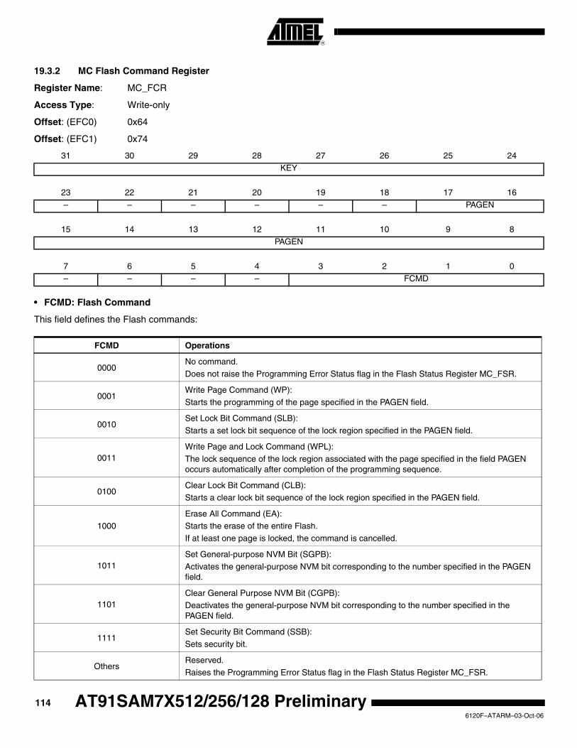
19.3.2 MC Flash Command Register
Register Name: MC_FCR
Access Type: Write-only
Offset: (EFC0) 0x64
Offset: (EFC1) 0x74
• FCMD: Flash Command
This field defines the Flash commands:
31 30 29 28 27 26 25 24
KEY
23 22 21 20 19 18 17 16
– – – – – – PAGEN
15 14 13 12 11 10 9 8
PAGEN
7 6 5 4 3 2 1 0
– – – – FCMD
FCMD Operations
0000No command.
Does not raise the Programming Error Status flag in the Flash Status Register MC_FSR.
0001Write Page Command (WP):
Starts the programming of the page specified in the PAGEN field.
0010Set Lock Bit Command (SLB):
Starts a set lock bit sequence of the lock region specified in the PAGEN field.
0011Write Page and Lock Command (WPL):
The lock sequence of the lock region associated with the page specified in the field PAGEN occurs automatically after completion of the programming sequence.
0100Clear Lock Bit Command (CLB):Starts a clear lock bit sequence of the lock region specified in the PAGEN field.
1000Erase All Command (EA):Starts the erase of the entire Flash.
If at least one page is locked, the command is cancelled.
1011Set General-purpose NVM Bit (SGPB):
Activates the general-purpose NVM bit corresponding to the number specified in the PAGEN field.
1101Clear General Purpose NVM Bit (CGPB):Deactivates the general-purpose NVM bit corresponding to the number specified in the PAGEN field.
1111Set Security Bit Command (SSB):
Sets security bit.
OthersReserved.
Raises the Programming Error Status flag in the Flash Status Register MC_FSR.
1146120F–ATARM–03-Oct-06
AT91SAM7X512/256/128 Preliminary

AT91SAM7X512/256/128 Preliminary
• PAGEN: Page Number
Note: Depending on the command, all the possible unused bits of PAGEN are meaningless.
• KEY: Write Protection Key
This field should be written with the value 0x5A to enable the command defined by the bits of the register. If the field is writ-ten with a different value, the write is not performed and no action is started.
Command PAGEN Description
Write Page Command PAGEN defines the page number to be written.
Write Page and Lock CommandPAGEN defines the page number to be written and its associated lock region.
Erase All Command This field is meaningless
Set/Clear Lock Bit CommandPAGEN defines one page number of the lock region to be locked or unlocked.
Set/Clear General Purpose NVM Bit Command PAGEN defines the general-purpose bit number.
Set Security Bit Command This field is meaningless
1156120F–ATARM–03-Oct-06
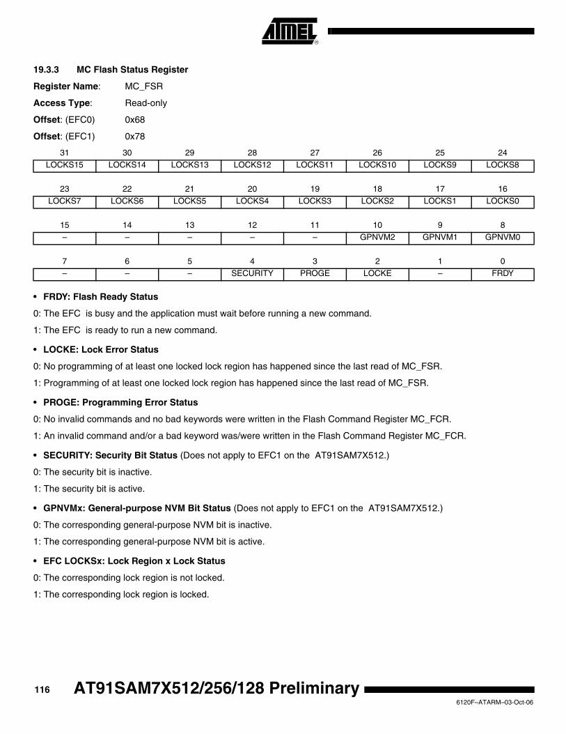
19.3.3 MC Flash Status Register
Register Name: MC_FSR
Access Type: Read-only
Offset: (EFC0) 0x68
Offset: (EFC1) 0x78
• FRDY: Flash Ready Status
0: The EFC is busy and the application must wait before running a new command.
1: The EFC is ready to run a new command.
• LOCKE: Lock Error Status
0: No programming of at least one locked lock region has happened since the last read of MC_FSR.
1: Programming of at least one locked lock region has happened since the last read of MC_FSR.
• PROGE: Programming Error Status
0: No invalid commands and no bad keywords were written in the Flash Command Register MC_FCR.
1: An invalid command and/or a bad keyword was/were written in the Flash Command Register MC_FCR.
• SECURITY: Security Bit Status (Does not apply to EFC1 on the AT91SAM7X512.)
0: The security bit is inactive.
1: The security bit is active.
• GPNVMx: General-purpose NVM Bit Status (Does not apply to EFC1 on the AT91SAM7X512.)
0: The corresponding general-purpose NVM bit is inactive.
1: The corresponding general-purpose NVM bit is active.
• EFC LOCKSx: Lock Region x Lock Status
0: The corresponding lock region is not locked.
1: The corresponding lock region is locked.
31 30 29 28 27 26 25 24
LOCKS15 LOCKS14 LOCKS13 LOCKS12 LOCKS11 LOCKS10 LOCKS9 LOCKS8
23 22 21 20 19 18 17 16
LOCKS7 LOCKS6 LOCKS5 LOCKS4 LOCKS3 LOCKS2 LOCKS1 LOCKS0
15 14 13 12 11 10 9 8
– – – – – GPNVM2 GPNVM1 GPNVM0
7 6 5 4 3 2 1 0
– – – SECURITY PROGE LOCKE – FRDY
1166120F–ATARM–03-Oct-06
AT91SAM7X512/256/128 Preliminary

AT91SAM7X512/256/128 Preliminary
20. Fast Flash Programming Interface (FFPI)
20.1 DescriptionThe Fast Flash Programming Interface provides two solutions - parallel or serial - for high-vol-ume programming using a standard gang programmer. The parallel interface is fully handshaked and the device is considered to be a standard EEPROM. Additionally, the parallel protocol offers an optimized access to all the embedded Flash functionalities. The serial inter-face uses the standard IEEE 1149.1 JTAG protocol. It offers an optimized access to all the embedded Flash functionalities.
Although the Fast Flash Programming Mode is a dedicated mode for high volume program-ming, this mode not designed for in-situ programming.
20.2 Parallel Fast Flash Programming
20.2.1 Device ConfigurationIn Fast Flash Programming Mode, the device is in a specific test mode. Only a certain set of pins is significant. Other pins must be left unconnected.
Figure 20-1. Parallel Programming Interface
NCMD PGMNCMDRDY PGMRDY
NOE PGMNOE
NVALID PGMNVALID
MODE[3:0] PGMM[3:0]
DATA[15:0] PGMD[15:0]
XIN
TSTVDDIOPGMEN0
PGMEN1
0 - 50MHz
VDDIO
VDDCORE
VDDIO
VDDPLL
VDDFLASH
GND
VDDIO
1176120F–ATARM–03-Oct-06
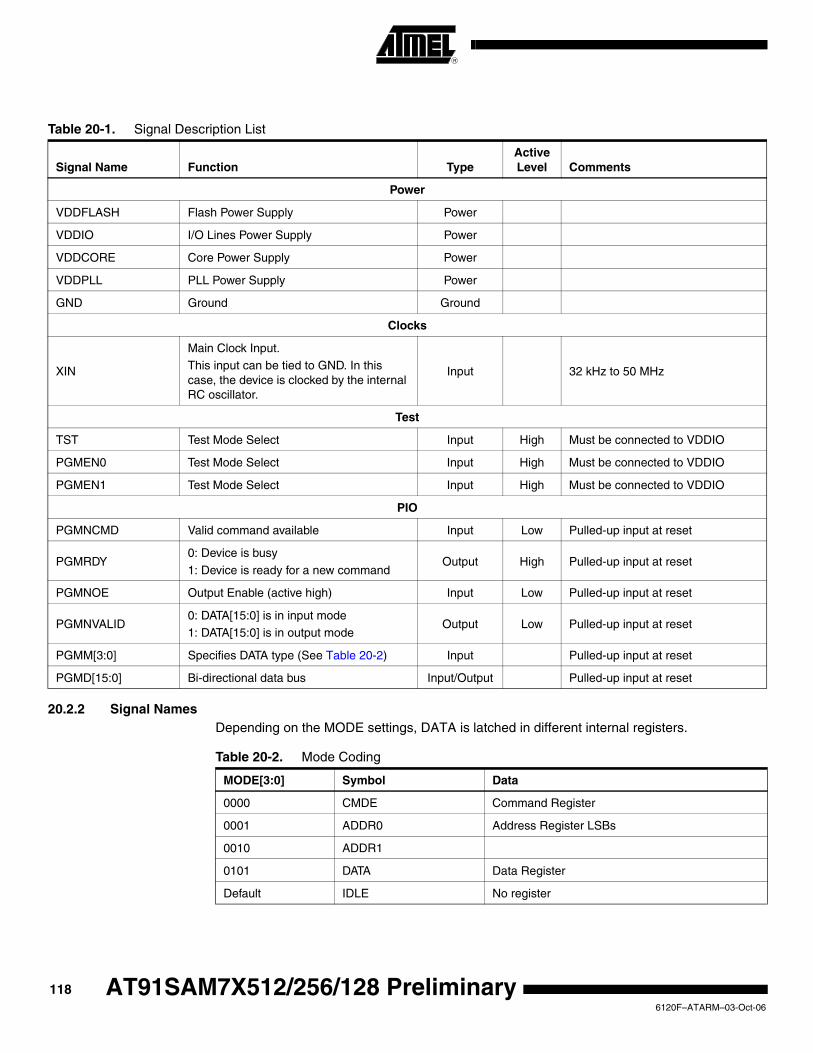
20.2.2 Signal NamesDepending on the MODE settings, DATA is latched in different internal registers.
Table 20-1. Signal Description List
Signal Name Function TypeActive Level Comments
Power
VDDFLASH Flash Power Supply Power
VDDIO I/O Lines Power Supply Power
VDDCORE Core Power Supply Power
VDDPLL PLL Power Supply Power
GND Ground Ground
Clocks
XIN
Main Clock Input.This input can be tied to GND. In this case, the device is clocked by the internal RC oscillator.
Input 32 kHz to 50 MHz
Test
TST Test Mode Select Input High Must be connected to VDDIO
PGMEN0 Test Mode Select Input High Must be connected to VDDIO
PGMEN1 Test Mode Select Input High Must be connected to VDDIO
PIO
PGMNCMD Valid command available Input Low Pulled-up input at reset
PGMRDY0: Device is busy
1: Device is ready for a new commandOutput High Pulled-up input at reset
PGMNOE Output Enable (active high) Input Low Pulled-up input at reset
PGMNVALID0: DATA[15:0] is in input mode1: DATA[15:0] is in output mode
Output Low Pulled-up input at reset
PGMM[3:0] Specifies DATA type (See Table 20-2) Input Pulled-up input at reset
PGMD[15:0] Bi-directional data bus Input/Output Pulled-up input at reset
Table 20-2. Mode Coding
MODE[3:0] Symbol Data
0000 CMDE Command Register
0001 ADDR0 Address Register LSBs
0010 ADDR1
0101 DATA Data Register
Default IDLE No register
1186120F–ATARM–03-Oct-06
AT91SAM7X512/256/128 Preliminary
AT91SAM7X512/256/128 Preliminary
When MODE is equal to CMDE, then a new command (strobed on DATA[15:0] signals) is stored in the command register.
Note: 1. Applies to AT91SAM7X512.
20.2.3 Entering Programming ModeThe following algorithm puts the device in Parallel Programming Mode:
• Apply GND, VDDIO, VDDCORE, VDDFLASH and VDDPLL.
• Apply XIN clock within TPOR_RESET if an external clock is available.
• Wait for TPOR_RESET
• Start a read or write handshaking.
Note: After reset, the device is clocked by the internal RC oscillator. Before clearing RDY signal, if an external clock ( > 32 kHz) is connected to XIN, then the device switches on the external clock. Else, XIN input is not considered. A higher frequency on XIN speeds up the programmer handshake.
20.2.4 Programmer HandshakingAn handshake is defined for read and write operations. When the device is ready to start a new operation (RDY signal set), the programmer starts the handshake by clearing the NCMD signal. The handshaking is achieved once NCMD signal is high and RDY is high.
20.2.4.1 Write HandshakingFor details on the write handshaking sequence, refer to Figure 20-2 and Table 20-4.
Table 20-3. Command Bit Coding
DATA[15:0] Symbol Command Executed
0x0011 READ Read Flash
0x0012 WP Write Page Flash
0x0022 WPL Write Page and Lock Flash
0x0032 EWP Erase Page and Write Page
0x0042 EWPL Erase Page and Write Page then Lock
0x0013 EA Erase All
0x0014 SLB Set Lock Bit
0x0024 CLB Clear Lock Bit
0x0015 GLB Get Lock Bit
0x0034 SFB Set General Purpose NVM bit
0x0044 CFB Clear General Purpose NVM bit
0x0025 GFB Get General Purpose NVM bit
0x0054 SSE Set Security Bit
0x0035 GSE Get Security Bit
0x001F WRAM Write Memory
0x0016 SEFC Select EFC Controller(1)
0x001E GVE Get Version
1196120F–ATARM–03-Oct-06

Figure 20-2. Parallel Programming Timing, Write Sequence
20.2.4.2 Read HandshakingFor details on the read handshaking sequence, refer to Figure 20-3 and Table 20-5.
Figure 20-3. Parallel Programming Timing, Read Sequence
NCMD
RDY
NOE
NVALID
DATA[15:0]
MODE[3:0]
1
2
3
4
5
Table 20-4. Write Handshake
Step Programmer Action Device Action Data I/O
1 Sets MODE and DATA signals Waits for NCMD low Input
2 Clears NCMD signal Latches MODE and DATA Input
3 Waits for RDY low Clears RDY signal Input
4 Releases MODE and DATA signals Executes command and polls NCMD high Input
5 Sets NCMD signal Executes command and polls NCMD high Input
6 Waits for RDY high Sets RDY Input
NCMD
RDY
NOE
NVALID
DATA[15:0]
MODE[3:0]
1
2
3
4
5
6
7
9
8
ADDR
Adress IN Z Data OUT
10
11
X IN
12
13
1206120F–ATARM–03-Oct-06
AT91SAM7X512/256/128 Preliminary
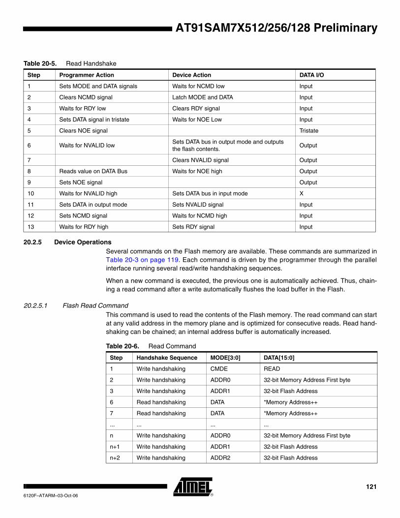
AT91SAM7X512/256/128 Preliminary
20.2.5 Device OperationsSeveral commands on the Flash memory are available. These commands are summarized in Table 20-3 on page 119. Each command is driven by the programmer through the parallel interface running several read/write handshaking sequences.
When a new command is executed, the previous one is automatically achieved. Thus, chain-ing a read command after a write automatically flushes the load buffer in the Flash.
20.2.5.1 Flash Read CommandThis command is used to read the contents of the Flash memory. The read command can start at any valid address in the memory plane and is optimized for consecutive reads. Read hand-shaking can be chained; an internal address buffer is automatically increased.
Table 20-5. Read Handshake
Step Programmer Action Device Action DATA I/O
1 Sets MODE and DATA signals Waits for NCMD low Input
2 Clears NCMD signal Latch MODE and DATA Input
3 Waits for RDY low Clears RDY signal Input
4 Sets DATA signal in tristate Waits for NOE Low Input
5 Clears NOE signal Tristate
6 Waits for NVALID lowSets DATA bus in output mode and outputs the flash contents.
Output
7 Clears NVALID signal Output
8 Reads value on DATA Bus Waits for NOE high Output
9 Sets NOE signal Output
10 Waits for NVALID high Sets DATA bus in input mode X
11 Sets DATA in output mode Sets NVALID signal Input
12 Sets NCMD signal Waits for NCMD high Input
13 Waits for RDY high Sets RDY signal Input
Table 20-6. Read Command
Step Handshake Sequence MODE[3:0] DATA[15:0]
1 Write handshaking CMDE READ
2 Write handshaking ADDR0 32-bit Memory Address First byte
3 Write handshaking ADDR1 32-bit Flash Address
6 Read handshaking DATA *Memory Address++
7 Read handshaking DATA *Memory Address++
... ... ... ...
n Write handshaking ADDR0 32-bit Memory Address First byte
n+1 Write handshaking ADDR1 32-bit Flash Address
n+2 Write handshaking ADDR2 32-bit Flash Address
1216120F–ATARM–03-Oct-06
20.2.5.2 Flash Write CommandThis command is used to write the Flash contents.
The Flash memory plane is organized into several pages. Data to be written are stored in a load buffer that corresponds to a Flash memory page. The load buffer is automatically flushed to the Flash:
• before access to any page other than the current one
• when a new command is validated (MODE = CMDE)
The Write Page command (WP) is optimized for consecutive writes. Write handshaking can be chained; an internal address buffer is automatically increased.
The Flash command Write Page and Lock (WPL) is equivalent to the Flash Write Command. However, the lock bit is automatically set at the end of the Flash write operation. As a lock region is composed of several pages, the programmer writes to the first pages of the lock region using Flash write commands and writes to the last page of the lock region using a Flash write and lock command.
n+3 Write handshaking ADDR3 32-bit Flash Address Last Byte
n+4 Read handshaking DATA *Memory Address++
n+5 Read handshaking DATA *Memory Address++
... ... ... ...
Table 20-6. Read Command (Continued)
Step Handshake Sequence MODE[3:0] DATA[15:0]
Table 20-7. Write Command
Step Handshake Sequence MODE[3:0] DATA[15:0]
1 Write handshaking CMDE WP or WPL or EWP or EWPL
2 Write handshaking ADDR0 32-bit Memory Address First byte
3 Write handshaking ADDR1 32-bit Flash Address
4 Write handshaking ADDR2 32-bit Flash Address
5 Write handshaking ADDR3 32-bit Flash Address Last Byte
6 Write handshaking DATA *Memory Address++
7 Write handshaking DATA *Memory Address++
... ... ... ...
n Write handshaking ADDR0 32-bit Memory Address First byte
n+1 Write handshaking ADDR1 32-bit Flash Address
n+2 Write handshaking ADDR2 32-bit Flash Address
n+3 Write handshaking ADDR3 32-bit Flash Address Last Byte
n+4 Write handshaking DATA *Memory Address++
n+5 Write handshaking DATA *Memory Address++
... ... ... ...
1226120F–ATARM–03-Oct-06
AT91SAM7X512/256/128 Preliminary
AT91SAM7X512/256/128 Preliminary
The Flash command Erase Page and Write (EWP) is equivalent to the Flash Write Com-mand. However, before programming the load buffer, the page is erased.
The Flash command Erase Page and Write the Lock (EWPL) combines EWP and WPL commands.
20.2.5.3 Flash Full Erase CommandThis command is used to erase the Flash memory planes.
All lock regions must be unlocked before the Full Erase command by using the CLB com-mand. Otherwise, the erase command is aborted and no page is erased.
20.2.5.4 Flash Lock CommandsLock bits can be set using WPL or EWPL commands. They can also be set by using the Set Lock command (SLB). With this command, several lock bits can be activated. A Bit Mask is provided as argument to the command. When bit 0 of the bit mask is set, then the first lock bit is activated.
In the same way, the Clear Lock command (CLB) is used to clear lock bits. All the lock bits are also cleared by the EA command.
Lock bits can be read using Get Lock Bit command (GLB). The nth lock bit is active when the bit n of the bit mask is set..
20.2.5.5 Flash General-purpose NVM CommandsGeneral-purpose NVM bits (GP NVM bits) can be set using the Set Fuse command (SFB). This command also activates GP NVM bits. A bit mask is provided as argument to the com-mand. When bit 0 of the bit mask is set, then the first GP NVM bit is activated.
Table 20-8. Full Erase Command
Step Handshake Sequence MODE[3:0] DATA[15:0]
1 Write handshaking CMDE EA
2 Write handshaking DATA 0
Table 20-9. Set and Clear Lock Bit Command
Step Handshake Sequence MODE[3:0] DATA[15:0]
1 Write handshaking CMDE SLB or CLB
2 Write handshaking DATA Bit Mask
Table 20-10. Get Lock Bit Command
Step Handshake Sequence MODE[3:0] DATA[15:0]
1 Write handshaking CMDE GLB
2 Read handshaking DATALock Bit Mask Status0 = Lock bit is cleared
1 = Lock bit is set
1236120F–ATARM–03-Oct-06
In the same way, the Clear Fuse command (CFB) is used to clear general-purpose NVM bits. All the general-purpose NVM bits are also cleared by the EA command. The general-purpose NVM bit is deactivated when the corresponding bit in the pattern value is set to 1.
General-purpose NVM bits can be read using the Get Fuse Bit command (GFB). The nth GP NVM bit is active when bit n of the bit mask is set..
20.2.5.6 Flash Security Bit CommandA security bit can be set using the Set Security Bit command (SSE). Once the security bit is active, the Fast Flash programming is disabled. No other command can be run. An event on the Erase pin can erase the security bit once the contents of the Flash have been erased.
The AT91SAM7X512 security bit is controlled by the EFC0. To use the Set Security Bit com-mand, the EFC0 must be selected using the Select EFC command.
20.2.5.7 AT91SAM7X512 Select EFC CommandThe commands WPx, EA, xLB, xFB are executed using the current EFC controller. The default EFC controller is EFC0. The Select EFC command (SEFC) allows selection of the current EFC controller.
20.2.5.8 Memory Write CommandThis command is used to perform a write access to any memory location.
Table 20-11. Set/Clear GP NVM Command
Step Handshake Sequence MODE[3:0] DATA[15:0]
1 Write handshaking CMDE SFB or CFB
2 Write handshaking DATA GP NVM bit pattern value
Table 20-12. Get GP NVM Bit Command
Step Handshake Sequence MODE[3:0] DATA[15:0]
1 Write handshaking CMDE GFB
2 Read handshaking DATA
GP NVM Bit Mask Status
0 = GP NVM bit is cleared1 = GP NVM bit is set
Table 20-13. Set Security Bit Command
Step Handshake Sequence MODE[3:0] DATA[15:0]
1 Write handshaking CMDE SSE
2 Write handshaking DATA 0
Table 20-14. Select EFC Command
Step Handshake Sequence MODE[3:0] DATA[15:0]
1 Write handshaking CMDE SEFC
2 Write handshaking DATA0 = Select EFC0
1 = Select EFC1
1246120F–ATARM–03-Oct-06
AT91SAM7X512/256/128 Preliminary

AT91SAM7X512/256/128 Preliminary
The Memory Write command (WRAM) is optimized for consecutive writes. Write handshak-ing can be chained; an internal address buffer is automatically increased.
20.2.5.9 Get Version CommandThe Get Version (GVE) command retrieves the version of the FFPI interface.
Table 20-15. Write Command
Step Handshake Sequence MODE[3:0] DATA[15:0]
1 Write handshaking CMDE WRAM
2 Write handshaking ADDR0 32-bit Memory Address First byte
3 Write handshaking ADDR1 32-bit Flash Address
4 Write handshaking ADDR2 32-bit Flash Address
5 Write handshaking ADDR3 32-bit Flash Address Last Byte
6 Write handshaking DATA *Memory Address++
7 Write handshaking DATA *Memory Address++
... ... ... ...
n Write handshaking ADDR0 32-bit Memory Address First byte
n+1 Write handshaking ADDR1 32-bit Flash Address
n+2 Write handshaking ADDR2 32-bit Flash Address
n+3 Write handshaking ADDR3 32-bit Flash Address Last Byte
n+4 Write handshaking DATA *Memory Address++
n+5 Write handshaking DATA *Memory Address++
... ... ... ...
Table 20-16. Get Version Command
Step Handshake Sequence MODE[3:0] DATA[15:0]
1 Write handshaking CMDE GVE
2 Write handshaking DATA Version
1256120F–ATARM–03-Oct-06
20.3 Serial Fast Flash ProgrammingThe Serial Fast Flash programming interface is based on IEEE Std. 1149.1 “Standard Test Access Port and Boundary-Scan Architecture”. Refer to this standard for an explanation of terms used in this chapter and for a description of the TAP controller states.
In this mode, data read/written from/to the embedded Flash of the device are transmitted through the JTAG interface of the device.
20.3.1 Device Configuration
Figure 20-4. In Serial Fast Flash Programming Mode, the device is in a specific test mode. Only a distinct set of pins is significant. Other pins must be left unconnected.Serial Programing
TDI
TDO
TMS
TCK
XIN
TSTVDDIO
PGMEN0
PGMEN1
0-50MHz
VDDIO
VDDCORE
VDDIO
VDDPLL
VDDFLASH
GND
VDDIO
Table 20-17. Signal Description List
Signal Name Function TypeActive Level Comments
Power
VDDFLASH Flash Power Supply Power
VDDIO I/O Lines Power Supply Power
VDDCORE Core Power Supply Power
VDDPLL PLL Power Supply Power
GND Ground Ground
Clocks
XIN
Main Clock Input.
This input can be tied to GND. In this case, the device is clocked by the internal RC oscillator.
Input 32 kHz to 50 MHz
1266120F–ATARM–03-Oct-06
AT91SAM7X512/256/128 Preliminary
AT91SAM7X512/256/128 Preliminary
20.3.2 Entering Serial Programming ModeThe following algorithm puts the device in Serial Programming Mode:
• Apply GND, VDDIO, VDDCORE, VDDFLASH and VDDPLL.
• Apply XIN clock within TPOR_RESET + 32(TSCLK) if an external clock is available.
• Wait for TPOR_RESET.
• Reset the TAP controller clocking 5 TCK pulses with TMS set.
• Shift 0x2 into the IR register (IR is 4 bits long, LSB first) without going through the Run-Test-Idle state.
• Shift 0x2 into the DR register (DR is 4 bits long, LSB first) without going through the Run-Test-Idle state.
• Shift 0xC into the IR register (IR is 4 bits long, LSB first) without going through the Run-Test-Idle state.
Note: After reset, the device is clocked by the internal RC oscillator. Before clearing RDY signal, if an external clock ( > 32 kHz) is connected to XIN, then the device will switch on the external clock. Else, XIN input is not considered. A higher frequency on XIN speeds up the programmer handshake.
Test
TST Test Mode Select Input High Must be connected to VDDIO.
PGMEN0 Test Mode Select Input High Must be connected to VDDIO
PGMEN1 Test Mode Select Input High Must be connected to VDDIO
JTAG
TCK JTAG TCK Input - Pulled-up input at reset
TDI JTAG Test Data In Input - Pulled-up input at reset
TDO JTAG Test Data Out Output -
TMS JTAG Test Mode Select Input - Pulled-up input at reset
Table 20-17. Signal Description List (Continued)
Signal Name Function TypeActive Level Comments
Table 20-18. Reset TAP Controller and Go to Select-DR-Scan
TDI TMS TAP Controller State
X 1
X 1
X 1
X 1
X 1 Test-Logic Reset
X 0 Run-Test/Idle
X 1 Select-DR-Scan
1276120F–ATARM–03-Oct-06

20.3.3 Read/Write HandshakeThe read/write handshake is done by carrying out read/write operations on two registers of the device that are accessible through the JTAG:
• Debug Comms Control Register: DCCR
• Debug Comms Data Register: DCDR
Access to these registers is done through the TAP 38-bit DR register comprising a 32-bit data field, a 5-bit address field and a read/write bit. The data to be written is scanned into the 32-bit data field with the address of the register to the 5-bit address field and 1 to the read/write bit. A register is read by scanning its address into the address field and 0 into the read/write bit, going through the UPDATE-DR TAP state, then scanning out the data.
Refer to the ARM7TDMI reference manuel for more information on Comm channel operations.
Figure 20-5. TAP 8-bit DR Register
A read or write takes place when the TAP controller enters UPDATE-DR state. Refer to the IEEE 1149.1 for more details on JTAG operations.
• The address of the Debug Comms Control Register is 0x04.
• The address of the Debug Comms Data Register is 0x05. The Debug Comms Control Register is read-only and allows synchronized handshaking between the processor and the debugger.
– Bit 1 (W): Denotes whether the programmer can read a data through the Debug Comms Data Register. If the device is busy W = 0, then the programmer must poll until W = 1.
– Bit 0 (R): Denotes whether the programmer can send data from the Debug Comms Data Register. If R = 1, data previously placed there through the scan chain has not been collected by the device and so the programmer must wait.
The write handshake is done by polling the Debug Comms Control Register until the R bit is cleared. Once cleared, data can be written to the Debug Comms Data Register.
The read handshake is done by polling the Debug Comms Control Register until the W bit is set. Once set, data can be read in the Debug Comms Data Register.
20.3.4 Device OperationsSeveral commands on the Flash memory are available. These commands are summarized in Table 20-3 on page 119. Commands are run by the programmer through the serial interface that is reading and writing the Debug Comms Registers.
TDI TDO4 0r/w Address 31 Data 0
AddressDecoder
Debug Comms Control Register
Debug Comms Data Register
325
1286120F–ATARM–03-Oct-06
AT91SAM7X512/256/128 Preliminary

AT91SAM7X512/256/128 Preliminary
20.3.4.1 Flash Read CommandThis command is used to read the Flash contents. The memory map is accessible through this command. Memory is seen as an array of words (32-bit wide). The read command can start at any valid address in the memory plane. This address must be word-aligned. The address is automatically incremented.
20.3.4.2 Flash Write CommandThis command is used to write the Flash contents. The address transmitted must be a valid Flash address in the memory plane.
The Flash memory plane is organized into several pages. Data to be written is stored in a load buffer that corresponds to a Flash memory page. The load buffer is automatically flushed to the Flash:
• before access to any page than the current one
• at the end of the number of words transmitted
The Write Page command (WP) is optimized for consecutive writes. Write handshaking can be chained; an internal address buffer is automatically increased.
Flash Write Page and Lock command (WPL) is equivalent to the Flash Write Command. However, the lock bit is automatically set at the end of the Flash write operation. As a lock region is composed of several pages, the programmer writes to the first pages of the lock region using Flash write commands and writes to the last page of the lock region using a Flash write and lock command.
Flash Erase Page and Write command (EWP) is equivalent to the Flash Write Command. However, before programming the load buffer, the page is erased.
Flash Erase Page and Write the Lock command (EWPL) combines EWP and WPL commands.
Table 20-19. Read Command
Read/Write DR Data
Write (Number of Words to Read) << 16 | READ
Write Address
Read Memory [address]
Read Memory [address+4]
... ...
Read Memory [address+(Number of Words to Read - 1)* 4]
Table 20-20. Write Command
Read/Write DR Data
Write (Number of Words to Write) << 16 | (WP or WPL or EWP or EWPL)
Write Address
Write Memory [address]
Write Memory [address+4]
Write Memory [address+8]
Write Memory [address+(Number of Words to Write - 1)* 4]
1296120F–ATARM–03-Oct-06

20.3.4.3 Flash Full Erase CommandThis command is used to erase the Flash memory planes.
All lock bits must be deactivated before using the Full Erase command. This can be done by using the CLB command.
20.3.4.4 Flash Lock CommandsLock bits can be set using WPL or EWPL commands. They can also be set by using the Set Lock command (SLB). With this command, several lock bits can be activated at the same time. Bit 0 of Bit Mask corresponds to the first lock bit and so on.
In the same way, the Clear Lock command (CLB) is used to clear lock bits. All the lock bits can also be cleared by the EA command.
Lock bits can be read using Get Lock Bit command (GLB). When a bit set in the Bit Mask is returned, then the corresponding lock bit is active.
20.3.4.5 Flash General-purpose NVM CommandsGeneral-purpose NVM bits (GP NVM) can be set with the Set Fuse command (SFB). Using this command, several GP NVM bits can be activated at the same time. Bit 0 of Bit Mask cor-responds to the first fuse bit and so on.
In the same way, the Clear Fuse command (CFB) is used to clear GP NVM bits. All the gen-eral-purpose NVM bits are also cleared by the EA command.
Table 20-21. Full Erase Command
Read/Write DR Data
Write EA
Table 20-22. Set and Clear Lock Bit Command
Read/Write DR Data
Write SLB or CLB
Write Bit Mask
Table 20-23. Get Lock Bit Command
Read/Write DR Data
Write GLB
Read Bit Mask
Table 20-24. Set and Clear General-purpose NVM Bit Command
Read/Write DR Data
Write SFB or CFB
Write Bit Mask
1306120F–ATARM–03-Oct-06
AT91SAM7X512/256/128 Preliminary
AT91SAM7X512/256/128 Preliminary
GP NVM bits can be read using Get Fuse Bit command (GFB). When a bit set in the Bit Mask is returned, then the corresponding fuse bit is set.
20.3.4.6 Flash Security Bit CommandSecurity bits can be set using Set Security Bit command (SSE). Once the security bit is active, the Fast Flash programming is disabled. No other command can be run. Only an event on the Erase pin can erase the security bit once the contents of the Flash have been erased.
The AT91SAM7X512 security bit is controlled by the EFC0. To use the Set Security Bit com-mand, the EFC0 must be selected using the Select EFC command.
20.3.4.7 AT91SAM7X512 Select EFC CommandThe commands WPx, EA, xLB, xFB are executed using the current EFC controller. The default EFC controller is EFC0. The Select EFC command (SEFC) allows selection of the current EFC controller.
20.3.4.8 Memory Write CommandThis command is used to perform a write access to any memory location.
The Memory Write command (WRAM) is optimized for consecutive writes. An internal address buffer is automatically increased.
Table 20-25. Get General-purpose NVM Bit Command
Read/Write DR Data
Write GFB
Read Bit Mask
Table 20-26. Set Security Bit Command
Read/Write DR Data
Write SSE
Table 20-27. Select EFC Command
Step Handshake Sequence MODE[3:0] DATA[15:0]
1 Write handshaking CMDE SEFC
2 Write handshaking DATA0 = Select EFC0
1 = Select EFC1
Table 20-28. Write Command
Read/Write DR Data
Write (Number of Words to Write) << 16 | (WRAM)
Write Address
Write Memory [address]
Write Memory [address+4]
Write Memory [address+8]
Write Memory [address+(Number of Words to Write - 1)* 4]
1316120F–ATARM–03-Oct-06

20.3.4.9 Get Version CommandThe Get Version (GVE) command retrieves the version of the FFPI interface.
Table 20-29. Get Version Command
Read/Write DR Data
Write GVE
Read Version
1326120F–ATARM–03-Oct-06
AT91SAM7X512/256/128 Preliminary
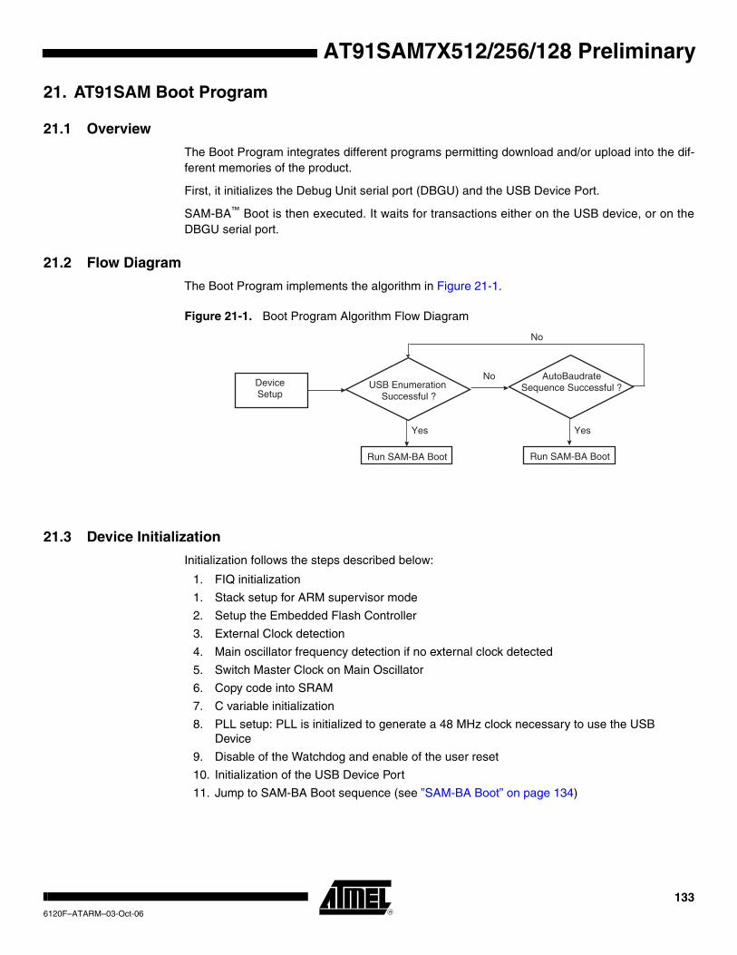
AT91SAM7X512/256/128 Preliminary
21. AT91SAM Boot Program
21.1 Overview
The Boot Program integrates different programs permitting download and/or upload into the dif-ferent memories of the product.
First, it initializes the Debug Unit serial port (DBGU) and the USB Device Port.
SAM-BA™ Boot is then executed. It waits for transactions either on the USB device, or on the DBGU serial port.
21.2 Flow Diagram
The Boot Program implements the algorithm in Figure 21-1.
Figure 21-1. Boot Program Algorithm Flow Diagram
21.3 Device Initialization
Initialization follows the steps described below:
1. FIQ initialization
1. Stack setup for ARM supervisor mode
2. Setup the Embedded Flash Controller
3. External Clock detection
4. Main oscillator frequency detection if no external clock detected
5. Switch Master Clock on Main Oscillator
6. Copy code into SRAM
7. C variable initialization
8. PLL setup: PLL is initialized to generate a 48 MHz clock necessary to use the USB Device
9. Disable of the Watchdog and enable of the user reset
10. Initialization of the USB Device Port
11. Jump to SAM-BA Boot sequence (see ”SAM-BA Boot” on page 134)
DeviceSetup
AutoBaudrateSequence Successful ?
Run SAM-BA Boot Run SAM-BA Boot
USB Enumeration Successful ?
Yes Yes
No
No
1336120F–ATARM–03-Oct-06
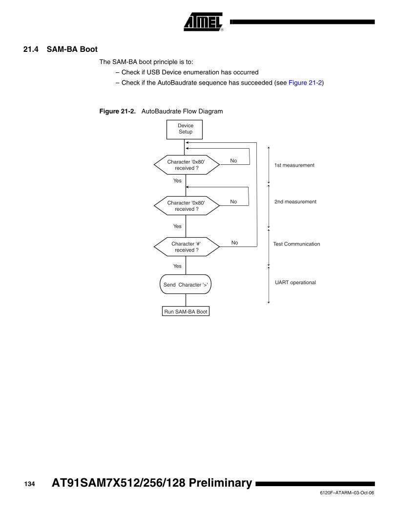
21.4 SAM-BA Boot
The SAM-BA boot principle is to:
– Check if USB Device enumeration has occurred
– Check if the AutoBaudrate sequence has succeeded (see Figure 21-2)
Figure 21-2. AutoBaudrate Flow Diagram
DeviceSetup
Character '0x80' received ?
No
Yes
Character '0x80' received ?
No
Yes
Character '#' received ?
Yes
Run SAM-BA Boot
Send Character '>'
No
1st measurement
2nd measurement
Test Communication
UART operational
1346120F–ATARM–03-Oct-06
AT91SAM7X512/256/128 Preliminary
AT91SAM7X512/256/128 Preliminary
– Once the communication interface is identified, the application runs in an infinite loop waiting for different commands as in Table 21-1.
• Write commands: Write a byte (O), a halfword (H) or a word (W) to the target.
– Address: Address in hexadecimal.
– Value: Byte, halfword or word to write in hexadecimal.
– Output: ‘>’.
• Read commands: Read a byte (o), a halfword (h) or a word (w) from the target.
– Address: Address in hexadecimal
– Output: The byte, halfword or word read in hexadecimal following by ‘>’
• Send a file (S): Send a file to a specified address
– Address: Address in hexadecimal
– Output: ‘>’.
Note: There is a time-out on this command which is reached when the prompt ‘>’ appears before the end of the command execution.
• Receive a file (R): Receive data into a file from a specified address
– Address: Address in hexadecimal
– NbOfBytes: Number of bytes in hexadecimal to receive
– Output: ‘>’
• Go (G): Jump to a specified address and execute the code
– Address: Address to jump in hexadecimal
– Output: ‘>’
• Get Version (V): Return the SAM-BA boot version
– Output: ‘>’
21.4.1 DBGU Serial Port
Communication is performed through the DBGU serial port initialized to 115200 Baud, 8, n, 1.
The Send and Receive File commands use the Xmodem protocol to communicate. Any terminal performing this protocol can be used to send the application file to the target. The size of the
Table 21-1. Commands Available through the SAM-BA Boot
Command Action Argument(s) Example
O write a byte Address, Value# O200001,CA#
o read a byte Address,# o200001,#
H write a half word Address, Value# H200002,CAFE#
h read a half word Address,# h200002,#
W write a word Address, Value# W200000,CAFEDECA#
w read a word Address,# w200000,#
S send a file Address,# S200000,#
R receive a file Address, NbOfBytes# R200000,1234#
G go Address# G200200#
V display version No argument V#
1356120F–ATARM–03-Oct-06
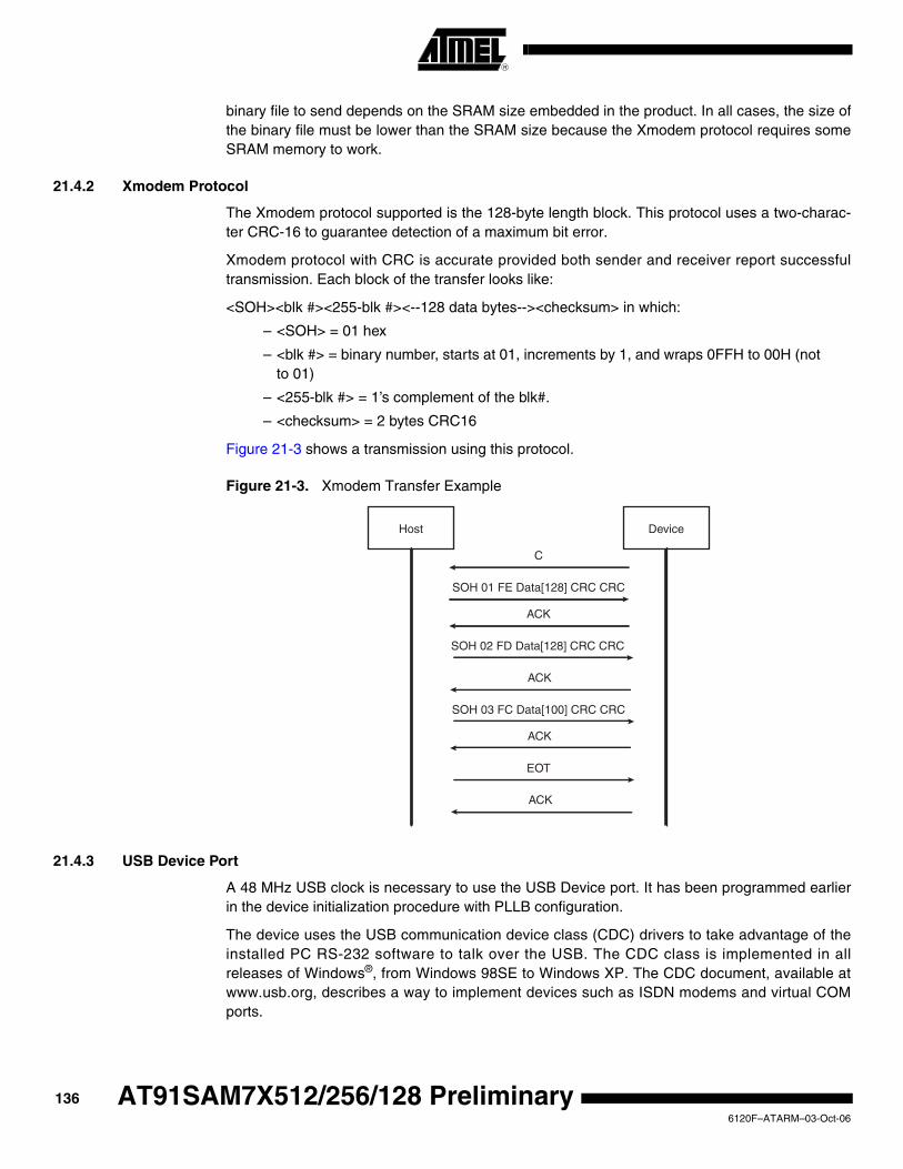
binary file to send depends on the SRAM size embedded in the product. In all cases, the size of the binary file must be lower than the SRAM size because the Xmodem protocol requires some SRAM memory to work.
21.4.2 Xmodem Protocol
The Xmodem protocol supported is the 128-byte length block. This protocol uses a two-charac-ter CRC-16 to guarantee detection of a maximum bit error.
Xmodem protocol with CRC is accurate provided both sender and receiver report successful transmission. Each block of the transfer looks like:
<SOH><blk #><255-blk #><--128 data bytes--><checksum> in which:
– <SOH> = 01 hex
– <blk #> = binary number, starts at 01, increments by 1, and wraps 0FFH to 00H (not to 01)
– <255-blk #> = 1’s complement of the blk#.
– <checksum> = 2 bytes CRC16
Figure 21-3 shows a transmission using this protocol.
Figure 21-3. Xmodem Transfer Example
21.4.3 USB Device Port
A 48 MHz USB clock is necessary to use the USB Device port. It has been programmed earlier in the device initialization procedure with PLLB configuration.
The device uses the USB communication device class (CDC) drivers to take advantage of the installed PC RS-232 software to talk over the USB. The CDC class is implemented in all releases of Windows®, from Windows 98SE to Windows XP. The CDC document, available at www.usb.org, describes a way to implement devices such as ISDN modems and virtual COM ports.
Host Device
SOH 01 FE Data[128] CRC CRC
C
ACK
SOH 02 FD Data[128] CRC CRC
ACK
SOH 03 FC Data[100] CRC CRC
ACK
EOT
ACK
1366120F–ATARM–03-Oct-06
AT91SAM7X512/256/128 Preliminary
AT91SAM7X512/256/128 Preliminary
The Vendor ID is Atmel’s vendor ID 0x03EB. The product ID is 0x6124. These references are used by the host operating system to mount the correct driver. On Windows systems, the INF files contain the correspondence between vendor ID and product ID.
Atmel provides an INF example to see the device as a new serial port and also provides another custom driver used by the SAM-BA application: atm6124.sys. Refer to the document “USB Basic Application”, literature number 6123, for more details.
21.4.3.1 Enumeration Process
The USB protocol is a master/slave protocol. This is the host that starts the enumeration send-ing requests to the device through the control endpoint. The device handles standard requests as defined in the USB Specification.
The device also handles some class requests defined in the CDC class.
Unhandled requests are STALLed.
21.4.3.2 Communication Endpoints
There are two communication endpoints and endpoint 0 is used for the enumeration process. Endpoint 1 is a 64-byte Bulk OUT endpoint and endpoint 2 is a 64-byte Bulk IN endpoint. SAM-BA Boot commands are sent by the host through the endpoint 1. If required, the message is split by the host into several data payloads by the host driver.
If the command requires a response, the host can send IN transactions to pick up the response.
Table 21-2. Handled Standard Requests
Request Definition
GET_DESCRIPTOR Returns the current device configuration value.
SET_ADDRESS Sets the device address for all future device access.
SET_CONFIGURATION Sets the device configuration.
GET_CONFIGURATION Returns the current device configuration value.
GET_STATUS Returns status for the specified recipient.
SET_FEATURE Used to set or enable a specific feature.
CLEAR_FEATURE Used to clear or disable a specific feature.
Table 21-3. Handled Class Requests
Request Definition
SET_LINE_CODINGConfigures DTE rate, stop bits, parity and number of character bits.
GET_LINE_CODINGRequests current DTE rate, stop bits, parity and number of character bits.
SET_CONTROL_LINE_STATERS-232 signal used to tell the DCE device the DTE device is now present.
1376120F–ATARM–03-Oct-06
21.5 Hardware and Software Constraints• SAM-BA boot copies itself in the SRAM and uses a block of internal SRAM for variables and
stacks. The remaining available size for the user code is 122880 bytes forAT91SAM7x512, 57344 bytes for AT91SAM7X256 and 24576 bytes for AT91SAM7X128.
• USB requirements:
– pull-up on DDP
– 18.432 MHz Quartz
Table 21-4. User Area Addresses
Device Start Address End Address Size (bytes)
AT91SAM7X512 0x202000 0x220000 122880
AT91SAM7X256 0x202000 0x210000 57344
AT91SAM7X128 0x202000 0x208000 24576
Table 21-5. Pins Driven during Boot Program Execution
Peripheral Pin PIO Line
DBGU DRXD DRXD_PIO
DBGU DTXD DTXD_PIO
1386120F–ATARM–03-Oct-06
AT91SAM7X512/256/128 Preliminary
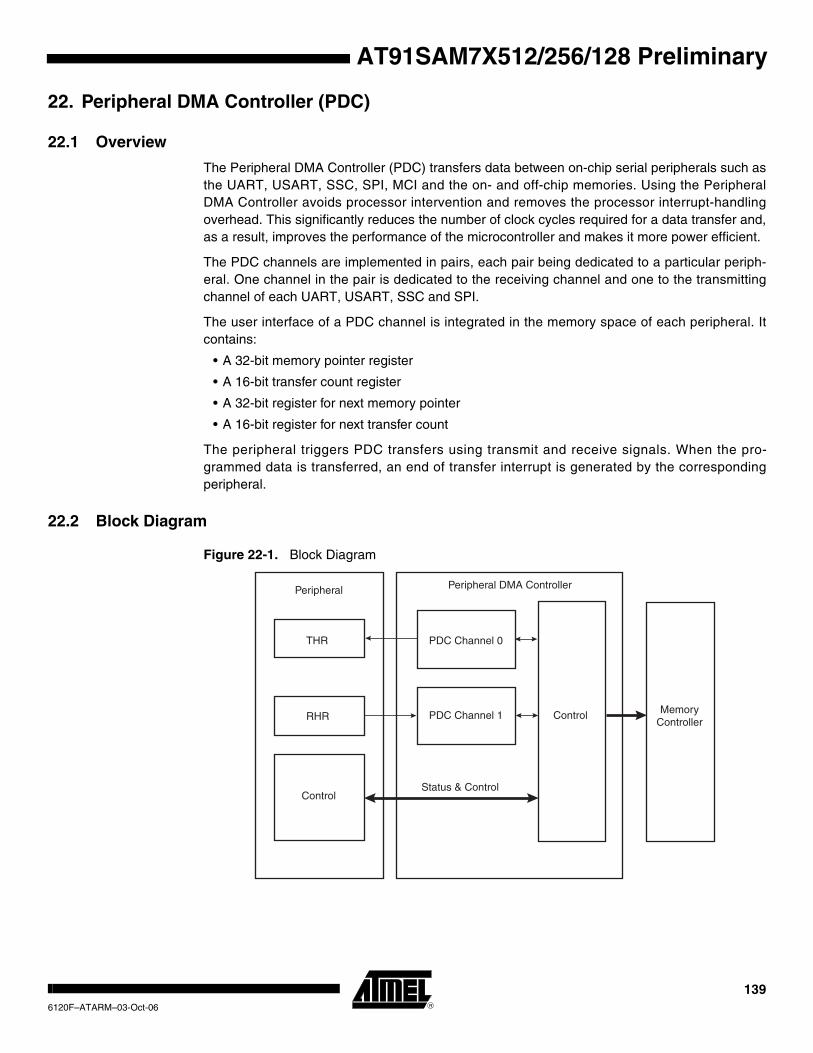
AT91SAM7X512/256/128 Preliminary
22. Peripheral DMA Controller (PDC)
22.1 Overview
The Peripheral DMA Controller (PDC) transfers data between on-chip serial peripherals such as the UART, USART, SSC, SPI, MCI and the on- and off-chip memories. Using the Peripheral DMA Controller avoids processor intervention and removes the processor interrupt-handling overhead. This significantly reduces the number of clock cycles required for a data transfer and, as a result, improves the performance of the microcontroller and makes it more power efficient.
The PDC channels are implemented in pairs, each pair being dedicated to a particular periph-eral. One channel in the pair is dedicated to the receiving channel and one to the transmitting channel of each UART, USART, SSC and SPI.
The user interface of a PDC channel is integrated in the memory space of each peripheral. It contains:
• A 32-bit memory pointer register
• A 16-bit transfer count register
• A 32-bit register for next memory pointer
• A 16-bit register for next transfer count
The peripheral triggers PDC transfers using transmit and receive signals. When the pro-grammed data is transferred, an end of transfer interrupt is generated by the corresponding peripheral.
22.2 Block Diagram
Figure 22-1. Block Diagram
Control
PDC Channel 0
PDC Channel 1
THR
RHR
ControlStatus & Control
Peripheral Peripheral DMA Controller
MemoryController
1396120F–ATARM–03-Oct-06
22.3 Functional Description
22.3.1 Configuration
The PDC channels user interface enables the user to configure and control the data transfers for each channel. The user interface of a PDC channel is integrated into the user interface of the peripheral (offset 0x100), which it is related to.
Per peripheral, it contains four 32-bit Pointer Registers (RPR, RNPR, TPR, and TNPR) and four 16-bit Counter Registers (RCR, RNCR, TCR, and TNCR).
The size of the buffer (number of transfers) is configured in an internal 16-bit transfer counter register, and it is possible, at any moment, to read the number of transfers left for each channel.
The memory base address is configured in a 32-bit memory pointer by defining the location of the first address to access in the memory. It is possible, at any moment, to read the location in memory of the next transfer and the number of remaining transfers. The PDC has dedicated sta-tus registers which indicate if the transfer is enabled or disabled for each channel. The status for each channel is located in the peripheral status register. Transfers can be enabled and/or dis-abled by setting TXTEN/TXTDIS and RXTEN/RXTDIS in PDC Transfer Control Register. These control bits enable reading the pointer and counter registers safely without any risk of their changing between both reads.
The PDC sends status flags to the peripheral visible in its status-register (ENDRX, ENDTX, RXBUFF, and TXBUFE).
ENDRX flag is set when the PERIPH_RCR register reaches zero.
RXBUFF flag is set when both PERIPH_RCR and PERIPH_RNCR reach zero.
ENDTX flag is set when the PERIPH_TCR register reaches zero.
TXBUFE flag is set when both PERIPH_TCR and PERIPH_TNCR reach zero.
These status flags are described in the peripheral status register.
22.3.2 Memory Pointers
Each peripheral is connected to the PDC by a receiver data channel and a transmitter data channel. Each channel has an internal 32-bit memory pointer. Each memory pointer points to a location anywhere in the memory space (on-chip memory or external bus interface memory).
Depending on the type of transfer (byte, half-word or word), the memory pointer is incremented by 1, 2 or 4, respectively for peripheral transfers.
If a memory pointer is reprogrammed while the PDC is in operation, the transfer address is changed, and the PDC performs transfers using the new address.
22.3.3 Transfer Counters
There is one internal 16-bit transfer counter for each channel used to count the size of the block already transferred by its associated channel. These counters are decremented after each data transfer. When the counter reaches zero, the transfer is complete and the PDC stops transfer-ring data.
If the Next Counter Register is equal to zero, the PDC disables the trigger while activating the related peripheral end flag.
1406120F–ATARM–03-Oct-06
AT91SAM7X512/256/128 Preliminary
AT91SAM7X512/256/128 Preliminary
If the counter is reprogrammed while the PDC is operating, the number of transfers is updated and the PDC counts transfers from the new value.
Programming the Next Counter/Pointer registers chains the buffers. The counters are decre-mented after each data transfer as stated above, but when the transfer counter reaches zero, the values of the Next Counter/Pointer are loaded into the Counter/Pointer registers in order to re-enable the triggers.
For each channel, two status bits indicate the end of the current buffer (ENDRX, ENTX) and the end of both current and next buffer (RXBUFF, TXBUFE). These bits are directly mapped to the peripheral status register and can trigger an interrupt request to the AIC.
The peripheral end flag is automatically cleared when one of the counter-registers (Counter or Next Counter Register) is written.
Note: When the Next Counter Register is loaded into the Counter Register, it is set to zero.
22.3.4 Data Transfers
The peripheral triggers PDC transfers using transmit (TXRDY) and receive (RXRDY) signals.
When the peripheral receives an external character, it sends a Receive Ready signal to the PDC which then requests access to the system bus. When access is granted, the PDC starts a read of the peripheral Receive Holding Register (RHR) and then triggers a write in the memory.
After each transfer, the relevant PDC memory pointer is incremented and the number of trans-fers left is decremented. When the memory block size is reached, a signal is sent to the peripheral and the transfer stops.
The same procedure is followed, in reverse, for transmit transfers.
22.3.5 Priority of PDC Transfer Requests
The Peripheral DMA Controller handles transfer requests from the channel according to priori-ties fixed for each product.These priorities are defined in the product datasheet.
If simultaneous requests of the same type (receiver or transmitter) occur on identical peripher-als, the priority is determined by the numbering of the peripherals.
If transfer requests are not simultaneous, they are treated in the order they occurred. Requests from the receivers are handled first and then followed by transmitter requests.
1416120F–ATARM–03-Oct-06
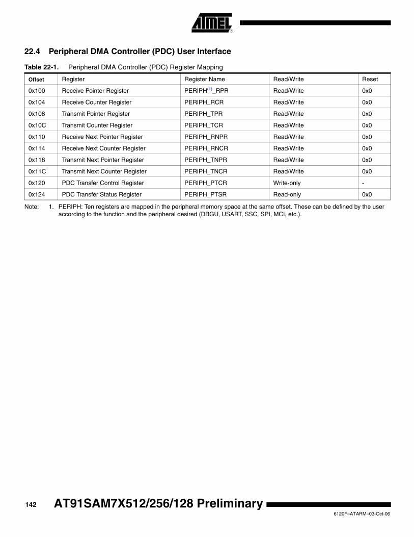
22.4 Peripheral DMA Controller (PDC) User Interface
Note: 1. PERIPH: Ten registers are mapped in the peripheral memory space at the same offset. These can be defined by the user according to the function and the peripheral desired (DBGU, USART, SSC, SPI, MCI, etc.).
Table 22-1. Peripheral DMA Controller (PDC) Register Mapping
Offset Register Register Name Read/Write Reset
0x100 Receive Pointer Register PERIPH(1)_RPR Read/Write 0x0
0x104 Receive Counter Register PERIPH_RCR Read/Write 0x0
0x108 Transmit Pointer Register PERIPH_TPR Read/Write 0x0
0x10C Transmit Counter Register PERIPH_TCR Read/Write 0x0
0x110 Receive Next Pointer Register PERIPH_RNPR Read/Write 0x0
0x114 Receive Next Counter Register PERIPH_RNCR Read/Write 0x0
0x118 Transmit Next Pointer Register PERIPH_TNPR Read/Write 0x0
0x11C Transmit Next Counter Register PERIPH_TNCR Read/Write 0x0
0x120 PDC Transfer Control Register PERIPH_PTCR Write-only -
0x124 PDC Transfer Status Register PERIPH_PTSR Read-only 0x0
1426120F–ATARM–03-Oct-06
AT91SAM7X512/256/128 Preliminary

AT91SAM7X512/256/128 Preliminary
22.4.1 PDC Receive Pointer Register
Register Name: PERIPH_RPR
Access Type: Read/Write
• RXPTR: Receive Pointer Address
Address of the next receive transfer.
22.4.2 PDC Receive Counter Register
Register Name: PERIPH_RCR
Access Type: Read/Write
• RXCTR: Receive Counter Value
Number of receive transfers to be performed.
31 30 29 28 27 26 25 24
RXPTR
23 22 21 20 19 18 17 16
RXPTR
15 14 13 12 11 10 9 8
RXPTR
7 6 5 4 3 2 1 0
RXPTR
31 30 29 28 27 26 25 24
--
23 22 21 20 19 18 17 16
--
15 14 13 12 11 10 9 8
RXCTR
7 6 5 4 3 2 1 0
RXCTR
1436120F–ATARM–03-Oct-06
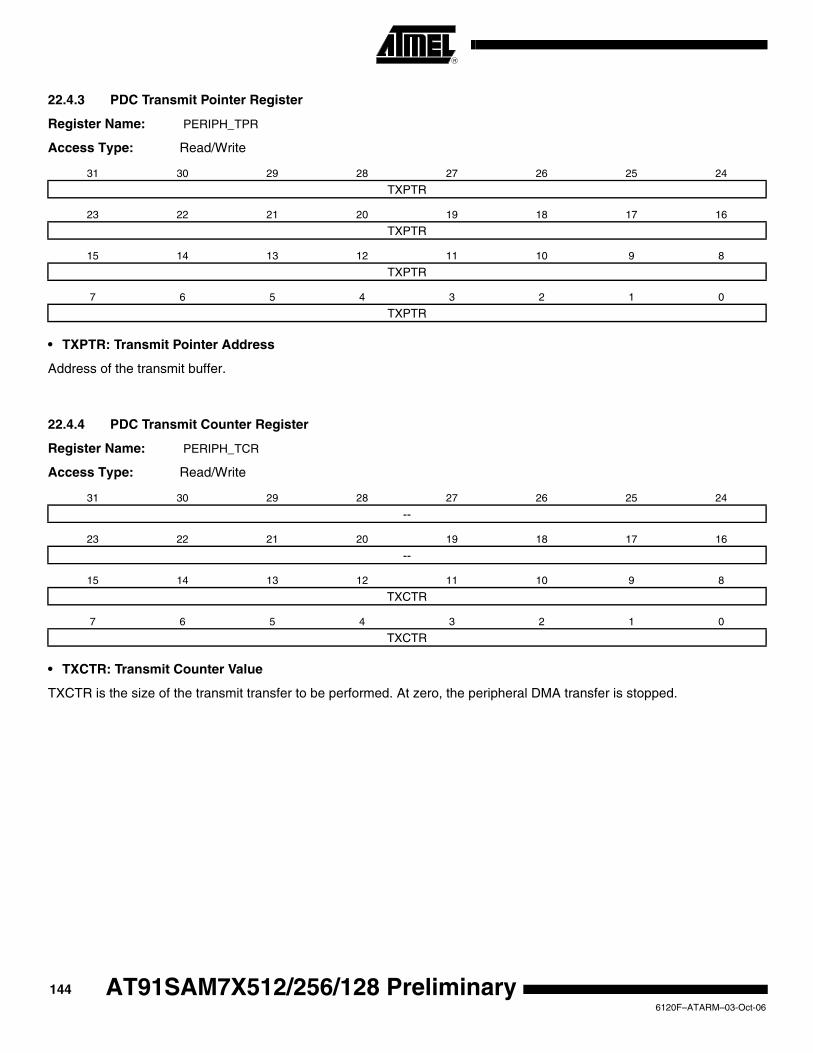
22.4.3 PDC Transmit Pointer Register
Register Name: PERIPH_TPR
Access Type: Read/Write
• TXPTR: Transmit Pointer Address
Address of the transmit buffer.
22.4.4 PDC Transmit Counter Register
Register Name: PERIPH_TCR
Access Type: Read/Write
• TXCTR: Transmit Counter Value
TXCTR is the size of the transmit transfer to be performed. At zero, the peripheral DMA transfer is stopped.
31 30 29 28 27 26 25 24
TXPTR
23 22 21 20 19 18 17 16
TXPTR
15 14 13 12 11 10 9 8
TXPTR
7 6 5 4 3 2 1 0
TXPTR
31 30 29 28 27 26 25 24
--
23 22 21 20 19 18 17 16
--
15 14 13 12 11 10 9 8
TXCTR
7 6 5 4 3 2 1 0
TXCTR
1446120F–ATARM–03-Oct-06
AT91SAM7X512/256/128 Preliminary

AT91SAM7X512/256/128 Preliminary
22.4.5 PDC Receive Next Pointer Register
Register Name: PERIPH_RNPR
Access Type: Read/Write
• RXNPTR: Receive Next Pointer Address
RXNPTR is the address of the next buffer to fill with received data when the current buffer is full.
22.4.6 PDC Receive Next Counter Register
Register Name: PERIPH_RNCR
Access Type: Read/Write
• RXNCR: Receive Next Counter Value
RXNCR is the size of the next buffer to receive.
31 30 29 28 27 26 25 24
RXNPTR
23 22 21 20 19 18 17 16
RXNPTR
15 14 13 12 11 10 9 8
RXNPTR
7 6 5 4 3 2 1 0
RXNPTR
31 30 29 28 27 26 25 24
--
23 22 21 20 19 18 17 16
--
15 14 13 12 11 10 9 8
RXNCR
7 6 5 4 3 2 1 0
RXNCR
1456120F–ATARM–03-Oct-06
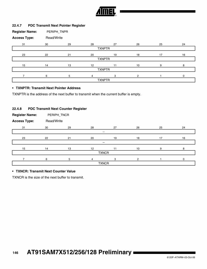
22.4.7 PDC Transmit Next Pointer Register
Register Name: PERIPH_TNPR
Access Type: Read/Write
• TXNPTR: Transmit Next Pointer Address
TXNPTR is the address of the next buffer to transmit when the current buffer is empty.
22.4.8 PDC Transmit Next Counter Register
Register Name: PERIPH_TNCR
Access Type: Read/Write
• TXNCR: Transmit Next Counter Value
TXNCR is the size of the next buffer to transmit.
31 30 29 28 27 26 25 24
TXNPTR
23 22 21 20 19 18 17 16
TXNPTR
15 14 13 12 11 10 9 8
TXNPTR
7 6 5 4 3 2 1 0
TXNPTR
31 30 29 28 27 26 25 24
--
23 22 21 20 19 18 17 16
--
15 14 13 12 11 10 9 8
TXNCR
7 6 5 4 3 2 1 0
TXNCR
1466120F–ATARM–03-Oct-06
AT91SAM7X512/256/128 Preliminary

AT91SAM7X512/256/128 Preliminary
22.4.9 PDC Transfer Control Register
Register Name: PERIPH_PTCR
Access Type: Write-only
• RXTEN: Receiver Transfer Enable
0 = No effect.
1 = Enables the receiver PDC transfer requests if RXTDIS is not set.
• RXTDIS: Receiver Transfer Disable
0 = No effect.
1 = Disables the receiver PDC transfer requests.
• TXTEN: Transmitter Transfer Enable
0 = No effect.
1 = Enables the transmitter PDC transfer requests.
• TXTDIS: Transmitter Transfer Disable
0 = No effect.
1 = Disables the transmitter PDC transfer requests
31 30 29 28 27 26 25 24
– – – – – – – –
23 22 21 20 19 18 17 16
– – – – – – – –
15 14 13 12 11 10 9 8
– – – – – – TXTDIS TXTEN
7 6 5 4 3 2 1 0
– – – – – – RXTDIS RXTEN
1476120F–ATARM–03-Oct-06

22.4.10 PDC Transfer Status Register
Register Name: PERIPH_PTSR
Access Type: Read-only
• RXTEN: Receiver Transfer Enable
0 = Receiver PDC transfer requests are disabled.
1 = Receiver PDC transfer requests are enabled.
• TXTEN: Transmitter Transfer Enable
0 = Transmitter PDC transfer requests are disabled.
1 = Transmitter PDC transfer requests are enabled.
31 30 29 28 27 26 25 24
– – – – – – – –
23 22 21 20 19 18 17 16
– – – – – – – –
15 14 13 12 11 10 9 8
– – – – – – – TXTEN
7 6 5 4 3 2 1 0
– – – – – – – RXTEN
1486120F–ATARM–03-Oct-06
AT91SAM7X512/256/128 Preliminary

AT91SAM7X512/256/128 Preliminary
23. Advanced Interrupt Controller (AIC)
23.1 Overview
The Advanced Interrupt Controller (AIC) is an 8-level priority, individually maskable, vectored interrupt controller, providing handling of up to thirty-two interrupt sources. It is designed to sub-stantially reduce the software and real-time overhead in handling internal and external interrupts.
The AIC drives the nFIQ (fast interrupt request) and the nIRQ (standard interrupt request) inputs of an ARM processor. Inputs of the AIC are either internal peripheral interrupts or external inter-rupts coming from the product's pins.
The 8-level Priority Controller allows the user to define the priority for each interrupt source, thus permitting higher priority interrupts to be serviced even if a lower priority interrupt is being treated.
Internal interrupt sources can be programmed to be level sensitive or edge triggered. External interrupt sources can be programmed to be positive-edge or negative-edge triggered or high-level or low-level sensitive.
The fast forcing feature redirects any internal or external interrupt source to provide a fast inter-rupt rather than a normal interrupt.
23.2 Block Diagram
Figure 23-1. Block Diagram
AIC
APB
ARMProcessor
FIQ
IRQ0-IRQn
EmbeddedPeripheralEE
PeripheralEmbeddedPeripheral
Embedded
Up to Thirty-twoSources
nFIQ
nIRQ
1496120F–ATARM–03-Oct-06
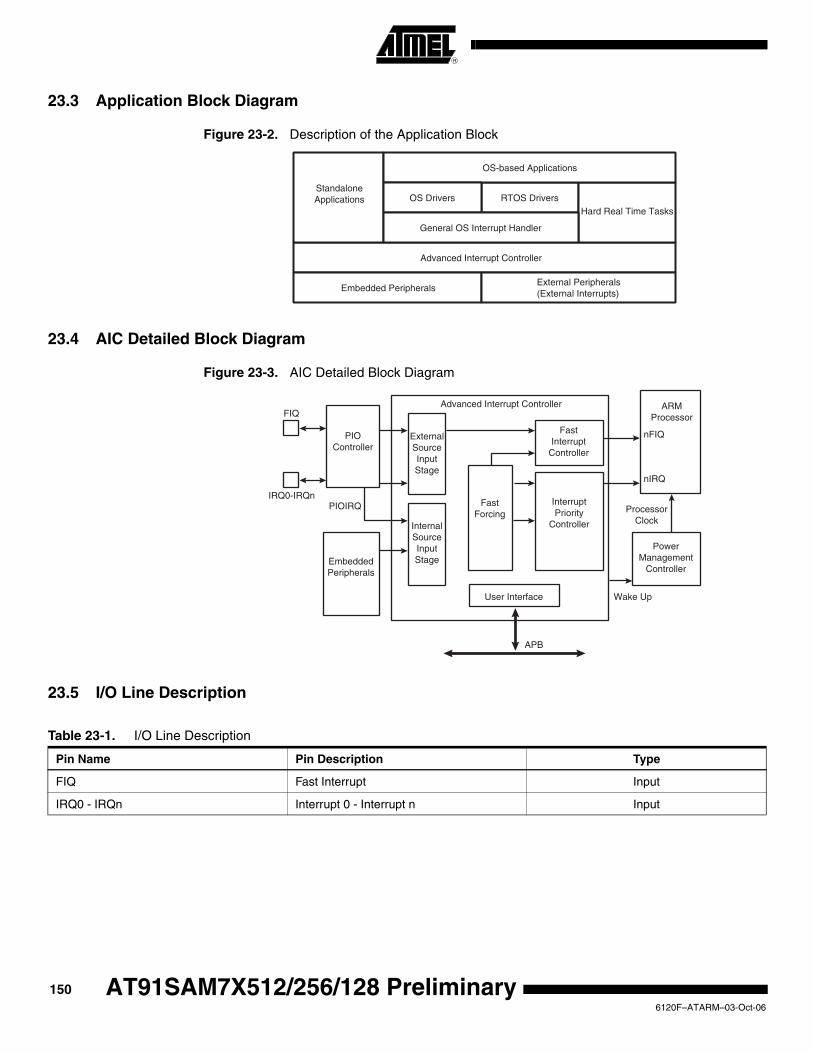
23.3 Application Block Diagram
Figure 23-2. Description of the Application Block
23.4 AIC Detailed Block Diagram
Figure 23-3. AIC Detailed Block Diagram
23.5 I/O Line Description
Advanced Interrupt Controller
Embedded PeripheralsExternal Peripherals(External Interrupts)
StandaloneApplications RTOS Drivers
Hard Real Time Tasks
OS-based Applications
OS Drivers
General OS Interrupt Handler
FIQ
PIOController
Advanced Interrupt Controller
IRQ0-IRQnPIOIRQ
EmbeddedPeripherals
ExternalSourceInputStage
InternalSourceInputStage
FastForcing
InterruptPriority
Controller
FastInterrupt
Controller
ARMProcessor
nFIQ
nIRQ
PowerManagement
Controller
Wake UpUser Interface
APB
ProcessorClock
Table 23-1. I/O Line Description
Pin Name Pin Description Type
FIQ Fast Interrupt Input
IRQ0 - IRQn Interrupt 0 - Interrupt n Input
1506120F–ATARM–03-Oct-06
AT91SAM7X512/256/128 Preliminary

AT91SAM7X512/256/128 Preliminary
23.6 Product Dependencies
23.6.1 I/O Lines
The interrupt signals FIQ and IRQ0 to IRQn are normally multiplexed through the PIO control-lers. Depending on the features of the PIO controller used in the product, the pins must be programmed in accordance with their assigned interrupt function. This is not applicable when the PIO controller used in the product is transparent on the input path.
23.6.2 Power Management
The Advanced Interrupt Controller is continuously clocked. The Power Management Controller has no effect on the Advanced Interrupt Controller behavior.
The assertion of the Advanced Interrupt Controller outputs, either nIRQ or nFIQ, wakes up the ARM processor while it is in Idle Mode. The General Interrupt Mask feature enables the AIC to wake up the processor without asserting the interrupt line of the processor, thus providing syn-chronization of the processor on an event.
23.6.3 Interrupt Sources
The Interrupt Source 0 is always located at FIQ. If the product does not feature an FIQ pin, the Interrupt Source 0 cannot be used.
The Interrupt Source 1 is always located at System Interrupt. This is the result of the OR-wiring of the system peripheral interrupt lines, such as the System Timer, the Real Time Clock, the Power Management Controller and the Memory Controller. When a system interrupt occurs, the service routine must first distinguish the cause of the interrupt. This is performed by reading suc-cessively the status registers of the above mentioned system peripherals.
The interrupt sources 2 to 31 can either be connected to the interrupt outputs of an embedded user peripheral or to external interrupt lines. The external interrupt lines can be connected directly, or through the PIO Controller.
The PIO Controllers are considered as user peripherals in the scope of interrupt handling. Accordingly, the PIO Controller interrupt lines are connected to the Interrupt Sources 2 to 31.
The peripheral identification defined at the product level corresponds to the interrupt source number (as well as the bit number controlling the clock of the peripheral). Consequently, to sim-plify the description of the functional operations and the user interface, the interrupt sources are named FIQ, SYS, and PID2 to PID31.
1516120F–ATARM–03-Oct-06

23.7 Functional Description
23.7.1 Interrupt Source Control
23.7.1.1 Interrupt Source Mode
The Advanced Interrupt Controller independently programs each interrupt source. The SRC-TYPE field of the corresponding AIC_SMR (Source Mode Register) selects the interrupt condition of each source.
The internal interrupt sources wired on the interrupt outputs of the embedded peripherals can be programmed either in level-sensitive mode or in edge-triggered mode. The active level of the internal interrupts is not important for the user.
The external interrupt sources can be programmed either in high level-sensitive or low level-sen-sitive modes, or in positive edge-triggered or negative edge-triggered modes.
23.7.1.2 Interrupt Source Enabling
Each interrupt source, including the FIQ in source 0, can be enabled or disabled by using the command registers; AIC_IECR (Interrupt Enable Command Register) and AIC_IDCR (Interrupt Disable Command Register). This set of registers conducts enabling or disabling in one instruc-tion. The interrupt mask can be read in the AIC_IMR register. A disabled interrupt does not affect servicing of other interrupts.
23.7.1.3 Interrupt Clearing and Setting
All interrupt sources programmed to be edge-triggered (including the FIQ in source 0) can be individually set or cleared by writing respectively the AIC_ISCR and AIC_ICCR registers. Clear-ing or setting interrupt sources programmed in level-sensitive mode has no effect.
The clear operation is perfunctory, as the software must perform an action to reinitialize the “memorization” circuitry activated when the source is programmed in edge-triggered mode. However, the set operation is available for auto-test or software debug purposes. It can also be used to execute an AIC-implementation of a software interrupt.
The AIC features an automatic clear of the current interrupt when the AIC_IVR (Interrupt Vector Register) is read. Only the interrupt source being detected by the AIC as the current interrupt is affected by this operation. (See “Priority Controller” on page 156.) The automatic clear reduces the operations required by the interrupt service routine entry code to reading the AIC_IVR. Note that the automatic interrupt clear is disabled if the interrupt source has the Fast Forcing feature enabled as it is considered uniquely as a FIQ source. (For further details, See “Fast Forcing” on page 160.)
The automatic clear of the interrupt source 0 is performed when AIC_FVR is read.
23.7.1.4 Interrupt Status
For each interrupt, the AIC operation originates in AIC_IPR (Interrupt Pending Register) and its mask in AIC_IMR (Interrupt Mask Register). AIC_IPR enables the actual activity of the sources, whether masked or not.
The AIC_ISR register reads the number of the current interrupt (see ”Priority Controller” on page 156) and the register AIC_CISR gives an image of the signals nIRQ and nFIQ driven on the processor.
1526120F–ATARM–03-Oct-06
AT91SAM7X512/256/128 Preliminary

AT91SAM7X512/256/128 Preliminary
Each status referred to above can be used to optimize the interrupt handling of the systems.
23.7.1.5 Internal Interrupt Source Input Stage
Figure 23-4. Internal Interrupt Source Input Stage
23.7.1.6 External Interrupt Source Input Stage
Figure 23-5. External Interrupt Source Input Stage
EdgeDetector
ClearSet
Source iAIC_IPR
AIC_IMR
AIC_IECR
AIC_IDCR
AIC_ISCR
AIC_ICCR
Fast Interrupt ControllerorPriority Controller
FF
Level/Edge
AIC_SMRI
(SRCTYPE)
EdgeDetector
ClearSet
Pos./Neg.
AIC_ISCR
AIC_ICCR
Source i
FF
Level/Edge
High/LowAIC_SMRi
SRCTYPE
AIC_IPR
AIC_IMR
AIC_IECR
AIC_IDCR
Fast Interrupt ControllerorPriority Controller
1536120F–ATARM–03-Oct-06

23.7.2 Interrupt Latencies
Global interrupt latencies depend on several parameters, including:
• The time the software masks the interrupts.
• Occurrence, either at the processor level or at the AIC level.
• The execution time of the instruction in progress when the interrupt occurs.
• The treatment of higher priority interrupts and the resynchronization of the hardware signals.
This section addresses only the hardware resynchronizations. It gives details of the latency times between the event on an external interrupt leading in a valid interrupt (edge or level) or the assertion of an internal interrupt source and the assertion of the nIRQ or nFIQ line on the pro-cessor. The resynchronization time depends on the programming of the interrupt source and on its type (internal or external). For the standard interrupt, resynchronization times are given assuming there is no higher priority in progress.
The PIO Controller multiplexing has no effect on the interrupt latencies of the external interrupt sources.
23.7.2.1 External Interrupt Edge Triggered Source
Figure 23-6. External Interrupt Edge Triggered Source
Maximum FIQ Latency = 4 Cycles
Maximum IRQ Latency = 4 Cycles
nFIQ
nIRQ
MCK
IRQ or FIQ(Positive Edge)
IRQ or FIQ(Negative Edge)
1546120F–ATARM–03-Oct-06
AT91SAM7X512/256/128 Preliminary
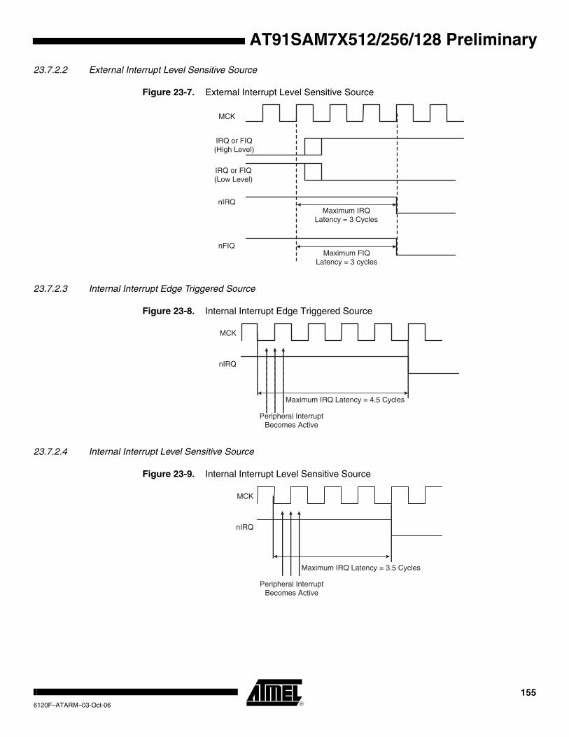
AT91SAM7X512/256/128 Preliminary
23.7.2.2 External Interrupt Level Sensitive Source
Figure 23-7. External Interrupt Level Sensitive Source
23.7.2.3 Internal Interrupt Edge Triggered Source
Figure 23-8. Internal Interrupt Edge Triggered Source
23.7.2.4 Internal Interrupt Level Sensitive Source
Figure 23-9. Internal Interrupt Level Sensitive Source
Maximum IRQLatency = 3 Cycles
Maximum FIQLatency = 3 cycles
MCK
IRQ or FIQ(High Level)
IRQ or FIQ(Low Level)
nIRQ
nFIQ
MCK
nIRQ
Peripheral InterruptBecomes Active
Maximum IRQ Latency = 4.5 Cycles
MCK
nIRQ
Maximum IRQ Latency = 3.5 Cycles
Peripheral InterruptBecomes Active
1556120F–ATARM–03-Oct-06
23.7.3 Normal Interrupt
23.7.3.1 Priority ControllerAn 8-level priority controller drives the nIRQ line of the processor, depending on the interrupt conditions occurring on the interrupt sources 1 to 31 (except for those programmed in Fast Forcing).
Each interrupt source has a programmable priority level of 7 to 0, which is user-definable by writ-ing the PRIOR field of the corresponding AIC_SMR (Source Mode Register). Level 7 is the highest priority and level 0 the lowest.
As soon as an interrupt condition occurs, as defined by the SRCTYPE field of the AIC_SMR (Source Mode Register), the nIRQ line is asserted. As a new interrupt condition might have hap-pened on other interrupt sources since the nIRQ has been asserted, the priority controller determines the current interrupt at the time the AIC_IVR (Interrupt Vector Register) is read. The read of AIC_IVR is the entry point of the interrupt handling which allows the AIC to consider that the interrupt has been taken into account by the software.
The current priority level is defined as the priority level of the current interrupt.
If several interrupt sources of equal priority are pending and enabled when the AIC_IVR is read, the interrupt with the lowest interrupt source number is serviced first.
The nIRQ line can be asserted only if an interrupt condition occurs on an interrupt source with a higher priority. If an interrupt condition happens (or is pending) during the interrupt treatment in progress, it is delayed until the software indicates to the AIC the end of the current service by writing the AIC_EOICR (End of Interrupt Command Register). The write of AIC_EOICR is the exit point of the interrupt handling.
23.7.3.2 Interrupt Nesting
The priority controller utilizes interrupt nesting in order for the high priority interrupt to be handled during the service of lower priority interrupts. This requires the interrupt service routines of the lower interrupts to re-enable the interrupt at the processor level.
When an interrupt of a higher priority happens during an already occurring interrupt service rou-tine, the nIRQ line is re-asserted. If the interrupt is enabled at the core level, the current execution is interrupted and the new interrupt service routine should read the AIC_IVR. At this time, the current interrupt number and its priority level are pushed into an embedded hardware stack, so that they are saved and restored when the higher priority interrupt servicing is finished and the AIC_EOICR is written.
The AIC is equipped with an 8-level wide hardware stack in order to support up to eight interrupt nestings pursuant to having eight priority levels.
23.7.3.3 Interrupt Vectoring
The interrupt handler addresses corresponding to each interrupt source can be stored in the reg-isters AIC_SVR1 to AIC_SVR31 (Source Vector Register 1 to 31). When the processor reads AIC_IVR (Interrupt Vector Register), the value written into AIC_SVR corresponding to the cur-rent interrupt is returned.
This feature offers a way to branch in one single instruction to the handler corresponding to the current interrupt, as AIC_IVR is mapped at the absolute address 0xFFFF F100 and thus acces-sible from the ARM interrupt vector at address 0x0000 0018 through the following instruction:
1566120F–ATARM–03-Oct-06
AT91SAM7X512/256/128 Preliminary
AT91SAM7X512/256/128 Preliminary
LDR PC,[PC,# -&F20]
When the processor executes this instruction, it loads the read value in AIC_IVR in its program counter, thus branching the execution on the correct interrupt handler.
This feature is often not used when the application is based on an operating system (either real time or not). Operating systems often have a single entry point for all the interrupts and the first task performed is to discern the source of the interrupt.
However, it is strongly recommended to port the operating system on AT91 products by support-ing the interrupt vectoring. This can be performed by defining all the AIC_SVR of the interrupt source to be handled by the operating system at the address of its interrupt handler. When doing so, the interrupt vectoring permits a critical interrupt to transfer the execution on a specific very fast handler and not onto the operating system’s general interrupt handler. This facilitates the support of hard real-time tasks (input/outputs of voice/audio buffers and software peripheral han-dling) to be handled efficiently and independently of the application running under an operating system.
23.7.3.4 Interrupt Handlers
This section gives an overview of the fast interrupt handling sequence when using the AIC. It is assumed that the programmer understands the architecture of the ARM processor, and espe-cially the processor interrupt modes and the associated status bits.
It is assumed that:
1. The Advanced Interrupt Controller has been programmed, AIC_SVR registers are loaded with corresponding interrupt service routine addresses and interrupts are enabled.
2. The instruction at the ARM interrupt exception vector address is required to work with the vectoring
LDR PC, [PC, # -&F20]
When nIRQ is asserted, if the bit “I” of CPSR is 0, the sequence is as follows:
1. The CPSR is stored in SPSR_irq, the current value of the Program Counter is loaded in the Interrupt link register (R14_irq) and the Program Counter (R15) is loaded with 0x18. In the following cycle during fetch at address 0x1C, the ARM core adjusts R14_irq, dec-rementing it by four.
2. The ARM core enters Interrupt mode, if it has not already done so.
3. When the instruction loaded at address 0x18 is executed, the program counter is loaded with the value read in AIC_IVR. Reading the AIC_IVR has the following effects:
– Sets the current interrupt to be the pending and enabled interrupt with the highest priority. The current level is the priority level of the current interrupt.
– De-asserts the nIRQ line on the processor. Even if vectoring is not used, AIC_IVR must be read in order to de-assert nIRQ.
– Automatically clears the interrupt, if it has been programmed to be edge-triggered.
– Pushes the current level and the current interrupt number on to the stack.
– Returns the value written in the AIC_SVR corresponding to the current interrupt.
4. The previous step has the effect of branching to the corresponding interrupt service routine. This should start by saving the link register (R14_irq) and SPSR_IRQ. The link register must be decremented by four when it is saved if it is to be restored directly into the program counter at the end of the interrupt. For example, the instruction SUB PC, LR, #4 may be used.
1576120F–ATARM–03-Oct-06
5. Further interrupts can then be unmasked by clearing the “I” bit in CPSR, allowing re-assertion of the nIRQ to be taken into account by the core. This can happen if an inter-rupt with a higher priority than the current interrupt occurs.
6. The interrupt handler can then proceed as required, saving the registers that will be used and restoring them at the end. During this phase, an interrupt of higher priority than the current level will restart the sequence from step 1.
Note: If the interrupt is programmed to be level sensitive, the source of the interrupt must be cleared dur-ing this phase.
7. The “I” bit in CPSR must be set in order to mask interrupts before exiting to ensure that the interrupt is completed in an orderly manner.
8. The End of Interrupt Command Register (AIC_EOICR) must be written in order to indi-cate to the AIC that the current interrupt is finished. This causes the current level to be popped from the stack, restoring the previous current level if one exists on the stack. If another interrupt is pending, with lower or equal priority than the old current level but with higher priority than the new current level, the nIRQ line is re-asserted, but the inter-rupt sequence does not immediately start because the “I” bit is set in the core. SPSR_irq is restored. Finally, the saved value of the link register is restored directly into the PC. This has the effect of returning from the interrupt to whatever was being exe-cuted before, and of loading the CPSR with the stored SPSR, masking or unmasking the interrupts depending on the state saved in SPSR_irq.
Note: The “I” bit in SPSR is significant. If it is set, it indicates that the ARM core was on the verge of masking an interrupt when the mask instruction was interrupted. Hence, when SPSR is restored, the mask instruction is completed (interrupt is masked).
1586120F–ATARM–03-Oct-06
AT91SAM7X512/256/128 Preliminary
AT91SAM7X512/256/128 Preliminary
23.7.4 Fast Interrupt
23.7.4.1 Fast Interrupt Source
The interrupt source 0 is the only source which can raise a fast interrupt request to the processor except if fast forcing is used. The interrupt source 0 is generally connected to a FIQ pin of the product, either directly or through a PIO Controller.
23.7.4.2 Fast Interrupt Control
The fast interrupt logic of the AIC has no priority controller. The mode of interrupt source 0 is programmed with the AIC_SMR0 and the field PRIOR of this register is not used even if it reads what has been written. The field SRCTYPE of AIC_SMR0 enables programming the fast inter-rupt source to be positive-edge triggered or negative-edge triggered or high-level sensitive or low-level sensitive
Writing 0x1 in the AIC_IECR (Interrupt Enable Command Register) and AIC_IDCR (Interrupt Disable Command Register) respectively enables and disables the fast interrupt. The bit 0 of AIC_IMR (Interrupt Mask Register) indicates whether the fast interrupt is enabled or disabled.
23.7.4.3 Fast Interrupt Vectoring
The fast interrupt handler address can be stored in AIC_SVR0 (Source Vector Register 0). The value written into this register is returned when the processor reads AIC_FVR (Fast Vector Reg-ister). This offers a way to branch in one single instruction to the interrupt handler, as AIC_FVR is mapped at the absolute address 0xFFFF F104 and thus accessible from the ARM fast inter-rupt vector at address 0x0000 001C through the following instruction:
LDR PC,[PC,# -&F20]
When the processor executes this instruction it loads the value read in AIC_FVR in its program counter, thus branching the execution on the fast interrupt handler. It also automatically per-forms the clear of the fast interrupt source if it is programmed in edge-triggered mode.
23.7.4.4 Fast Interrupt Handlers
This section gives an overview of the fast interrupt handling sequence when using the AIC. It is assumed that the programmer understands the architecture of the ARM processor, and espe-cially the processor interrupt modes and associated status bits.
Assuming that:
1. The Advanced Interrupt Controller has been programmed, AIC_SVR0 is loaded with the fast interrupt service routine address, and the interrupt source 0 is enabled.
2. The Instruction at address 0x1C (FIQ exception vector address) is required to vector the fast interrupt:
LDR PC, [PC, # -&F20]
3. The user does not need nested fast interrupts.
When nFIQ is asserted, if the bit “F” of CPSR is 0, the sequence is:
1. The CPSR is stored in SPSR_fiq, the current value of the program counter is loaded in the FIQ link register (R14_FIQ) and the program counter (R15) is loaded with 0x1C. In the following cycle, during fetch at address 0x20, the ARM core adjusts R14_fiq, decre-menting it by four.
2. The ARM core enters FIQ mode.
1596120F–ATARM–03-Oct-06

3. When the instruction loaded at address 0x1C is executed, the program counter is loaded with the value read in AIC_FVR. Reading the AIC_FVR has effect of automati-cally clearing the fast interrupt, if it has been programmed to be edge triggered. In this case only, it de-asserts the nFIQ line on the processor.
4. The previous step enables branching to the corresponding interrupt service routine. It is not necessary to save the link register R14_fiq and SPSR_fiq if nested fast interrupts are not needed.
5. The Interrupt Handler can then proceed as required. It is not necessary to save regis-ters R8 to R13 because FIQ mode has its own dedicated registers and the user R8 to R13 are banked. The other registers, R0 to R7, must be saved before being used, and restored at the end (before the next step). Note that if the fast interrupt is programmed to be level sensitive, the source of the interrupt must be cleared during this phase in order to de-assert the interrupt source 0.
6. Finally, the Link Register R14_fiq is restored into the PC after decrementing it by four (with instruction SUB PC, LR, #4 for example). This has the effect of returning from the interrupt to whatever was being executed before, loading the CPSR with the SPSR and masking or unmasking the fast interrupt depending on the state saved in the SPSR.
Note: The “F” bit in SPSR is significant. If it is set, it indicates that the ARM core was just about to mask FIQ interrupts when the mask instruction was interrupted. Hence when the SPSR is restored, the interrupted instruction is completed (FIQ is masked).
Another way to handle the fast interrupt is to map the interrupt service routine at the address of the ARM vector 0x1C. This method does not use the vectoring, so that reading AIC_FVR must be performed at the very beginning of the handler operation. However, this method saves the execution of a branch instruction.
23.7.4.5 Fast ForcingThe Fast Forcing feature of the advanced interrupt controller provides redirection of any normal Interrupt source on the fast interrupt controller.
Fast Forcing is enabled or disabled by writing to the Fast Forcing Enable Register (AIC_FFER) and the Fast Forcing Disable Register (AIC_FFDR). Writing to these registers results in an update of the Fast Forcing Status Register (AIC_FFSR) that controls the feature for each inter-nal or external interrupt source.
When Fast Forcing is disabled, the interrupt sources are handled as described in the previous pages.
When Fast Forcing is enabled, the edge/level programming and, in certain cases, edge detec-tion of the interrupt source is still active but the source cannot trigger a normal interrupt to the processor and is not seen by the priority handler.
If the interrupt source is programmed in level-sensitive mode and an active level is sampled, Fast Forcing results in the assertion of the nFIQ line to the core.
If the interrupt source is programmed in edge-triggered mode and an active edge is detected, Fast Forcing results in the assertion of the nFIQ line to the core.
The Fast Forcing feature does not affect the Source 0 pending bit in the Interrupt Pending Reg-ister (AIC_IPR).
The FIQ Vector Register (AIC_FVR) reads the contents of the Source Vector Register 0 (AIC_SVR0), whatever the source of the fast interrupt may be. The read of the FVR does not
1606120F–ATARM–03-Oct-06
AT91SAM7X512/256/128 Preliminary

AT91SAM7X512/256/128 Preliminary
clear the Source 0 when the fast forcing feature is used and the interrupt source should be cleared by writing to the Interrupt Clear Command Register (AIC_ICCR).
All enabled and pending interrupt sources that have the fast forcing feature enabled and that are programmed in edge-triggered mode must be cleared by writing to the Interrupt Clear Command Register. In doing so, they are cleared independently and thus lost interrupts are prevented.
The read of AIC_IVR does not clear the source that has the fast forcing feature enabled.
The source 0, reserved to the fast interrupt, continues operating normally and becomes one of the Fast Interrupt sources.
Figure 23-10. Fast Forcing
Source 0 _ FIQ
Input Stage
Automatic Clear
Input Stage
Automatic Clear
Source n
AIC_IPR
AIC_IMR
AIC_FFSR
AIC_IPR
AIC_IMR
PriorityManager
nFIQ
nIRQ
Read IVR if Source n is the current interruptand if Fast Forcing is disabled on Source n.
Read FVR if Fast Forcing is disabled on Sources 1 to 31.
1616120F–ATARM–03-Oct-06

23.7.5 Protect Mode
The Protect Mode permits reading the Interrupt Vector Register without performing the associ-ated automatic operations. This is necessary when working with a debug system. When a debugger, working either with a Debug Monitor or the ARM processor's ICE, stops the applica-tions and updates the opened windows, it might read the AIC User Interface and thus the IVR. This has undesirable consequences:
• If an enabled interrupt with a higher priority than the current one is pending, it is stacked.
• If there is no enabled pending interrupt, the spurious vector is returned.
In either case, an End of Interrupt command is necessary to acknowledge and to restore the context of the AIC. This operation is generally not performed by the debug system as the debug system would become strongly intrusive and cause the application to enter an undesired state.
This is avoided by using the Protect Mode. Writing DBGM in AIC_DCR (Debug Control Register) at 0x1 enables the Protect Mode.
When the Protect Mode is enabled, the AIC performs interrupt stacking only when a write access is performed on the AIC_IVR. Therefore, the Interrupt Service Routines must write (arbitrary data) to the AIC_IVR just after reading it. The new context of the AIC, including the value of the Interrupt Status Register (AIC_ISR), is updated with the current interrupt only when AIC_IVR is written.
An AIC_IVR read on its own (e.g., by a debugger), modifies neither the AIC context nor the AIC_ISR. Extra AIC_IVR reads perform the same operations. However, it is recommended to not stop the processor between the read and the write of AIC_IVR of the interrupt service routine to make sure the debugger does not modify the AIC context.
To summarize, in normal operating mode, the read of AIC_IVR performs the following opera-tions within the AIC:
1. Calculates active interrupt (higher than current or spurious).
2. Determines and returns the vector of the active interrupt.
3. Memorizes the interrupt.
4. Pushes the current priority level onto the internal stack.
5. Acknowledges the interrupt.
However, while the Protect Mode is activated, only operations 1 to 3 are performed when AIC_IVR is read. Operations 4 and 5 are only performed by the AIC when AIC_IVR is written.
Software that has been written and debugged using the Protect Mode runs correctly in Normal Mode without modification. However, in Normal Mode the AIC_IVR write has no effect and can be removed to optimize the code.
23.7.6 Spurious Interrupt
The Advanced Interrupt Controller features protection against spurious interrupts. A spurious interrupt is defined as being the assertion of an interrupt source long enough for the AIC to assert the nIRQ, but no longer present when AIC_IVR is read. This is most prone to occur when:
• An external interrupt source is programmed in level-sensitive mode and an active level occurs for only a short time.
1626120F–ATARM–03-Oct-06
AT91SAM7X512/256/128 Preliminary

AT91SAM7X512/256/128 Preliminary
• An internal interrupt source is programmed in level sensitive and the output signal of the corresponding embedded peripheral is activated for a short time. (As in the case for the Watchdog.)
• An interrupt occurs just a few cycles before the software begins to mask it, thus resulting in a pulse on the interrupt source.
The AIC detects a spurious interrupt at the time the AIC_IVR is read while no enabled interrupt source is pending. When this happens, the AIC returns the value stored by the programmer in AIC_SPU (Spurious Vector Register). The programmer must store the address of a spurious interrupt handler in AIC_SPU as part of the application, to enable an as fast as possible return to the normal execution flow. This handler writes in AIC_EOICR and performs a return from interrupt.
23.7.7 General Interrupt Mask
The AIC features a General Interrupt Mask bit to prevent interrupts from reaching the processor. Both the nIRQ and the nFIQ lines are driven to their inactive state if the bit GMSK in AIC_DCR (Debug Control Register) is set. However, this mask does not prevent waking up the processor if it has entered Idle Mode. This function facilitates synchronizing the processor on a next event and, as soon as the event occurs, performs subsequent operations without having to handle an interrupt. It is strongly recommended to use this mask with caution.
1636120F–ATARM–03-Oct-06

23.8 Advanced Interrupt Controller (AIC) User Interface
23.8.1 Base Address
The AIC is mapped at the address 0xFFFF F000. It has a total 4-Kbyte addressing space. This permits the vectoring feature, as the PC-relative load/store instructions of the ARM processor support only an ± 4-Kbyte offset.
23.8.2 Register Mapping
Notes: 1. The reset value of this register depends on the level of the external interrupt source. All other sources are cleared at reset, thus not pending.
2. PID2...PID31 bit fields refer to the identifiers as defined in the Peripheral Identifiers Section of the product datasheet.
Table 23-2. Register Mapping
Offset Register Name Access Reset Value
0000 Source Mode Register 0 AIC_SMR0 Read/Write 0x0
0x04 Source Mode Register 1 AIC_SMR1 Read/Write 0x0
--- --- --- --- ---
0x7C Source Mode Register 31 AIC_SMR31 Read/Write 0x0
0x80 Source Vector Register 0 AIC_SVR0 Read/Write 0x0
0x84 Source Vector Register 1 AIC_SVR1 Read/Write 0x0
--- --- --- --- ---
0xFC Source Vector Register 31 AIC_SVR31 Read/Write 0x0
0x100 Interrupt Vector Register AIC_IVR Read-only 0x0
0x104 FIQ Interrupt Vector Register AIC_FVR Read-only 0x0
0x108 Interrupt Status Register AIC_ISR Read-only 0x0
0x10C Interrupt Pending Register(2) AIC_IPR Read-only 0x0(1)
0x110 Interrupt Mask Register(2) AIC_IMR Read-only 0x0
0x114 Core Interrupt Status Register AIC_CISR Read-only 0x0
0x118 Reserved --- --- ---
0x11C Reserved --- --- ---
0x120 Interrupt Enable Command Register(2) AIC_IECR Write-only ---
0x124 Interrupt Disable Command Register(2) AIC_IDCR Write-only ---
0x128 Interrupt Clear Command Register(2) AIC_ICCR Write-only ---
0x12C Interrupt Set Command Register(2) AIC_ISCR Write-only ---
0x130 End of Interrupt Command Register AIC_EOICR Write-only ---
0x134 Spurious Interrupt Vector Register AIC_SPU Read/Write 0x0
0x138 Debug Control Register AIC_DCR Read/Write 0x0
0x13C Reserved --- --- ---
0x140 Fast Forcing Enable Register(2) AIC_FFER Write-only ---
0x144 Fast Forcing Disable Register(2) AIC_FFDR Write-only ---
0x148 Fast Forcing Status Register(2) AIC_FFSR Read-only 0x0
1646120F–ATARM–03-Oct-06
AT91SAM7X512/256/128 Preliminary

AT91SAM7X512/256/128 Preliminary
23.8.3 AIC Source Mode Register
Register Name: AIC_SMR0..AIC_SMR31
Access Type: Read/Write
Reset Value: 0x0
• PRIOR: Priority Level
Programs the priority level for all sources except FIQ source (source 0).
The priority level can be between 0 (lowest) and 7 (highest).
The priority level is not used for the FIQ in the related SMR register AIC_SMRx.
• SRCTYPE: Interrupt Source Type
The active level or edge is not programmable for the internal interrupt sources.
31 30 29 28 27 26 25 24
– – – – – – – –
23 22 21 20 19 18 17 16
– – – – – – – –
15 14 13 12 11 10 9 8
– – – – – – – –
7 6 5 4 3 2 1 0
– SRCTYPE – – PRIOR
SRCTYPE Internal Interrupt Sources External Interrupt Sources
0 0 High level Sensitive Low level Sensitive
0 1 Positive edge triggered Negative edge triggered
1 0 High level Sensitive High level Sensitive
1 1 Positive edge triggered Positive edge triggered
1656120F–ATARM–03-Oct-06
23.8.4 AIC Source Vector Register
Register Name: AIC_SVR0..AIC_SVR31
Access Type: Read/Write
Reset Value: 0x0
• VECTOR: Source Vector
The user may store in these registers the addresses of the corresponding handler for each interrupt source.
23.8.5 AIC Interrupt Vector Register
Register Name: AIC_IVR
Access Type: Read-only
Reset Value: 0
• IRQV: Interrupt Vector Register
The Interrupt Vector Register contains the vector programmed by the user in the Source Vector Register corresponding to the current interrupt.
The Source Vector Register is indexed using the current interrupt number when the Interrupt Vector Register is read.
When there is no current interrupt, the Interrupt Vector Register reads the value stored in AIC_SPU.
31 30 29 28 27 26 25 24
VECTOR
23 22 21 20 19 18 17 16
VECTOR
15 14 13 12 11 10 9 8
VECTOR
7 6 5 4 3 2 1 0
VECTOR
31 30 29 28 27 26 25 24
IRQV
23 22 21 20 19 18 17 16
IRQV
15 14 13 12 11 10 9 8
IRQV
7 6 5 4 3 2 1 0
IRQV
1666120F–ATARM–03-Oct-06
AT91SAM7X512/256/128 Preliminary
AT91SAM7X512/256/128 Preliminary
23.8.6 AIC FIQ Vector Register
Register Name: AIC_FVR
Access Type: Read-only
Reset Value: 0
• FIQV: FIQ Vector Register
The FIQ Vector Register contains the vector programmed by the user in the Source Vector Register 0. When there is no fast interrupt, the FIQ Vector Register reads the value stored in AIC_SPU.
23.8.7 AIC Interrupt Status Register
Register Name: AIC_ISR
Access Type: Read-only
Reset Value: 0
• IRQID: Current Interrupt Identifier
The Interrupt Status Register returns the current interrupt source number.
31 30 29 28 27 26 25 24
FIQV
23 22 21 20 19 18 17 16
FIQV
15 14 13 12 11 10 9 8
FIQV
7 6 5 4 3 2 1 0
FIQV
31 30 29 28 27 26 25 24
– – – – – – – –
23 22 21 20 19 18 17 16
– – – – – – – –
15 14 13 12 11 10 9 8
– – – – – – – –
7 6 5 4 3 2 1 0
– – – IRQID
1676120F–ATARM–03-Oct-06

23.8.8 AIC Interrupt Pending Register
Register Name: AIC_IPR
Access Type: Read-only
Reset Value: 0
• FIQ, SYS, PID2-PID31: Interrupt Pending
0 = Corresponding interrupt is not pending.
1 = Corresponding interrupt is pending.
23.8.9 AIC Interrupt Mask Register
Register Name: AIC_IMR
Access Type: Read-only
Reset Value: 0
• FIQ, SYS, PID2-PID31: Interrupt Mask
0 = Corresponding interrupt is disabled.
1 = Corresponding interrupt is enabled.
31 30 29 28 27 26 25 24
PID31 PID30 PID29 PID28 PID27 PID26 PID25 PID24
23 22 21 20 19 18 17 16
PID23 PID22 PID21 PID20 PID19 PID18 PID17 PID16
15 14 13 12 11 10 9 8
PID15 PID14 PID13 PID12 PID11 PID10 PID9 PID8
7 6 5 4 3 2 1 0
PID7 PID6 PID5 PID4 PID3 PID2 SYS FIQ
31 30 29 28 27 26 25 24
PID31 PID30 PID29 PID28 PID27 PID26 PID25 PID24
23 22 21 20 19 18 17 16
PID23 PID22 PID21 PID20 PID19 PID18 PID17 PID16
15 14 13 12 11 10 9 8
PID15 PID14 PID13 PID12 PID11 PID10 PID9 PID8
7 6 5 4 3 2 1 0
PID7 PID6 PID5 PID4 PID3 PID2 SYS FIQ
1686120F–ATARM–03-Oct-06
AT91SAM7X512/256/128 Preliminary
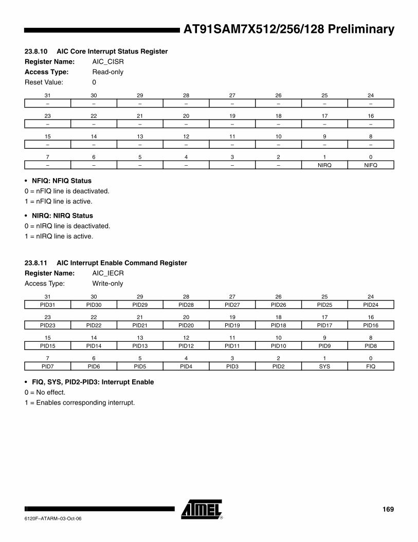
AT91SAM7X512/256/128 Preliminary
23.8.10 AIC Core Interrupt Status Register
Register Name: AIC_CISR
Access Type: Read-only
Reset Value: 0
• NFIQ: NFIQ Status
0 = nFIQ line is deactivated.
1 = nFIQ line is active.
• NIRQ: NIRQ Status
0 = nIRQ line is deactivated.
1 = nIRQ line is active.
23.8.11 AIC Interrupt Enable Command Register
Register Name: AIC_IECR
Access Type: Write-only
• FIQ, SYS, PID2-PID3: Interrupt Enable
0 = No effect.
1 = Enables corresponding interrupt.
31 30 29 28 27 26 25 24
– – – – – – – –
23 22 21 20 19 18 17 16
– – – – – – – –
15 14 13 12 11 10 9 8
– – – – – – – –
7 6 5 4 3 2 1 0
– – – – – – NIRQ NIFQ
31 30 29 28 27 26 25 24
PID31 PID30 PID29 PID28 PID27 PID26 PID25 PID24
23 22 21 20 19 18 17 16
PID23 PID22 PID21 PID20 PID19 PID18 PID17 PID16
15 14 13 12 11 10 9 8
PID15 PID14 PID13 PID12 PID11 PID10 PID9 PID8
7 6 5 4 3 2 1 0
PID7 PID6 PID5 PID4 PID3 PID2 SYS FIQ
1696120F–ATARM–03-Oct-06

23.8.12 AIC Interrupt Disable Command Register
Register Name: AIC_IDCR
Access Type: Write-only
• FIQ, SYS, PID2-PID31: Interrupt Disable
0 = No effect.
1 = Disables corresponding interrupt.
23.8.13 AIC Interrupt Clear Command Register
Register Name: AIC_ICCR
Access Type: Write-only
• FIQ, SYS, PID2-PID31: Interrupt Clear
0 = No effect.
1 = Clears corresponding interrupt.
31 30 29 28 27 26 25 24
PID31 PID30 PID29 PID28 PID27 PID26 PID25 PID24
23 22 21 20 19 18 17 16
PID23 PID22 PID21 PID20 PID19 PID18 PID17 PID16
15 14 13 12 11 10 9 8
PID15 PID14 PID13 PID12 PID11 PID10 PID9 PID8
7 6 5 4 3 2 1 0
PID7 PID6 PID5 PID4 PID3 PID2 SYS FIQ
31 30 29 28 27 26 25 24
PID31 PID30 PID29 PID28 PID27 PID26 PID25 PID24
23 22 21 20 19 18 17 16
PID23 PID22 PID21 PID20 PID19 PID18 PID17 PID16
15 14 13 12 11 10 9 8
PID15 PID14 PID13 PID12 PID11 PID10 PID9 PID8
7 6 5 4 3 2 1 0
PID7 PID6 PID5 PID4 PID3 PID2 SYS FIQ
1706120F–ATARM–03-Oct-06
AT91SAM7X512/256/128 Preliminary
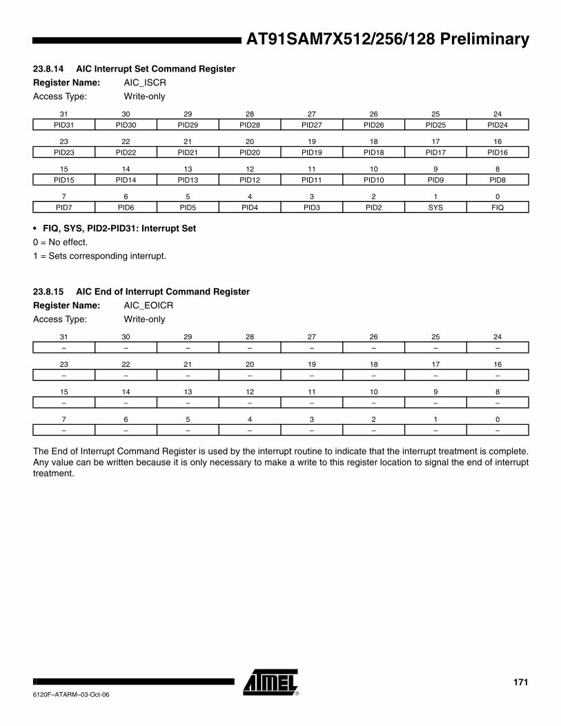
AT91SAM7X512/256/128 Preliminary
23.8.14 AIC Interrupt Set Command Register
Register Name: AIC_ISCR
Access Type: Write-only
• FIQ, SYS, PID2-PID31: Interrupt Set
0 = No effect.
1 = Sets corresponding interrupt.
23.8.15 AIC End of Interrupt Command Register
Register Name: AIC_EOICR
Access Type: Write-only
The End of Interrupt Command Register is used by the interrupt routine to indicate that the interrupt treatment is complete. Any value can be written because it is only necessary to make a write to this register location to signal the end of interrupt treatment.
31 30 29 28 27 26 25 24
PID31 PID30 PID29 PID28 PID27 PID26 PID25 PID24
23 22 21 20 19 18 17 16
PID23 PID22 PID21 PID20 PID19 PID18 PID17 PID16
15 14 13 12 11 10 9 8
PID15 PID14 PID13 PID12 PID11 PID10 PID9 PID8
7 6 5 4 3 2 1 0
PID7 PID6 PID5 PID4 PID3 PID2 SYS FIQ
31 30 29 28 27 26 25 24
– – – – – – – –
23 22 21 20 19 18 17 16
– – – – – – – –
15 14 13 12 11 10 9 8
– – – – – – – –
7 6 5 4 3 2 1 0
– – – – – – – –
1716120F–ATARM–03-Oct-06

23.8.16 AIC Spurious Interrupt Vector Register
Register Name: AIC_SPU
Access Type: Read/Write
Reset Value: 0
• SIQV: Spurious Interrupt Vector Register
The user may store the address of a spurious interrupt handler in this register. The written value is returned in AIC_IVR in case of a spurious interrupt and in AIC_FVR in case of a spurious fast interrupt.
23.8.17 AIC Debug Control Register
Register Name: AIC_DEBUG
Access Type: Read/Write
Reset Value: 0
• PROT: Protection Mode
0 = The Protection Mode is disabled.
1 = The Protection Mode is enabled.
• GMSK: General Mask
0 = The nIRQ and nFIQ lines are normally controlled by the AIC.
1 = The nIRQ and nFIQ lines are tied to their inactive state.
31 30 29 28 27 26 25 24
SIQV
23 22 21 20 19 18 17 16
SIQV
15 14 13 12 11 10 9 8
SIQV
7 6 5 4 3 2 1 0
SIQV
31 30 29 28 27 26 25 24
– – – – – – – –
23 22 21 20 19 18 17 16
– – – – – – – –
15 14 13 12 11 10 9 8
– – – – – – – –
7 6 5 4 3 2 1 0
– – – – – – GMSK PROT
1726120F–ATARM–03-Oct-06
AT91SAM7X512/256/128 Preliminary
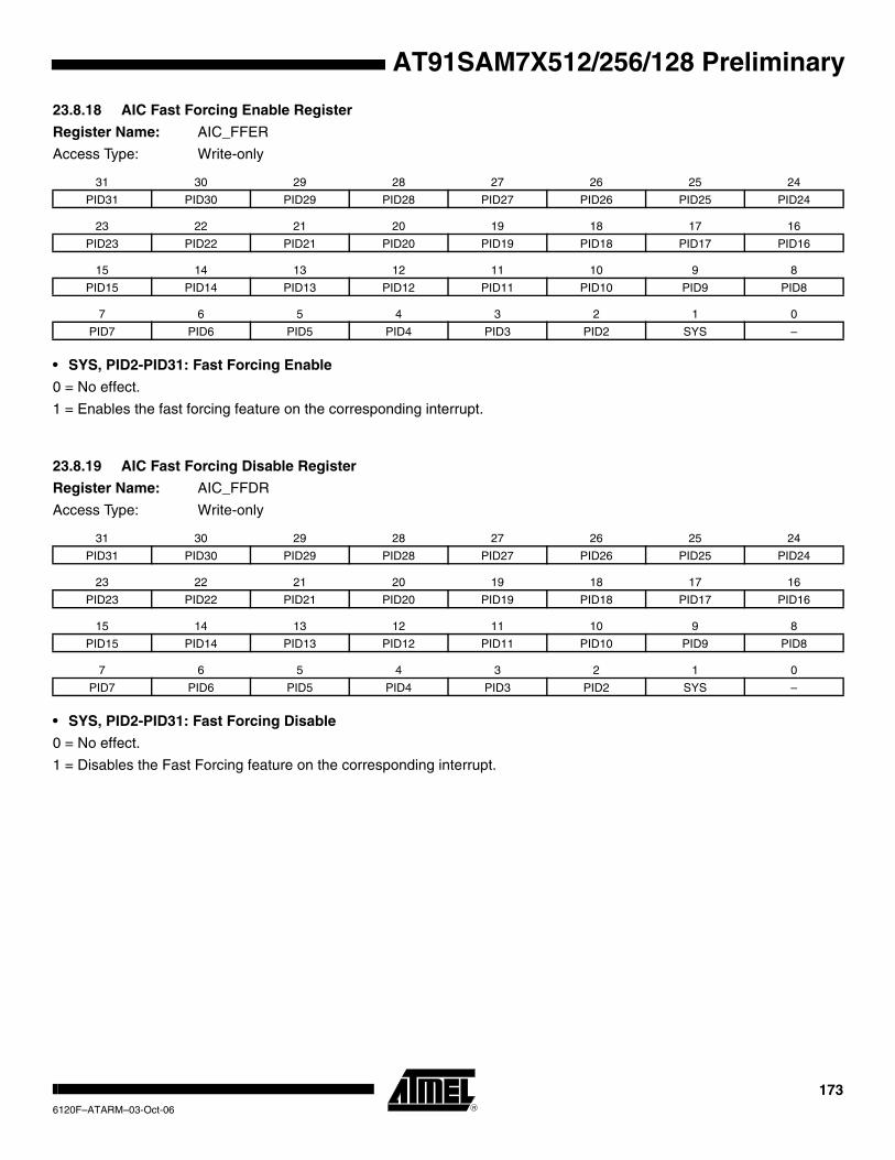
AT91SAM7X512/256/128 Preliminary
23.8.18 AIC Fast Forcing Enable Register
Register Name: AIC_FFER
Access Type: Write-only
• SYS, PID2-PID31: Fast Forcing Enable
0 = No effect.
1 = Enables the fast forcing feature on the corresponding interrupt.
23.8.19 AIC Fast Forcing Disable Register
Register Name: AIC_FFDR
Access Type: Write-only
• SYS, PID2-PID31: Fast Forcing Disable
0 = No effect.
1 = Disables the Fast Forcing feature on the corresponding interrupt.
31 30 29 28 27 26 25 24
PID31 PID30 PID29 PID28 PID27 PID26 PID25 PID24
23 22 21 20 19 18 17 16
PID23 PID22 PID21 PID20 PID19 PID18 PID17 PID16
15 14 13 12 11 10 9 8
PID15 PID14 PID13 PID12 PID11 PID10 PID9 PID8
7 6 5 4 3 2 1 0
PID7 PID6 PID5 PID4 PID3 PID2 SYS –
31 30 29 28 27 26 25 24
PID31 PID30 PID29 PID28 PID27 PID26 PID25 PID24
23 22 21 20 19 18 17 16
PID23 PID22 PID21 PID20 PID19 PID18 PID17 PID16
15 14 13 12 11 10 9 8
PID15 PID14 PID13 PID12 PID11 PID10 PID9 PID8
7 6 5 4 3 2 1 0
PID7 PID6 PID5 PID4 PID3 PID2 SYS –
1736120F–ATARM–03-Oct-06
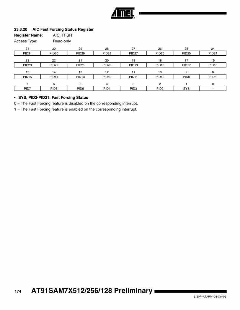
23.8.20 AIC Fast Forcing Status Register
Register Name: AIC_FFSR
Access Type: Read-only
• SYS, PID2-PID31: Fast Forcing Status
0 = The Fast Forcing feature is disabled on the corresponding interrupt.
1 = The Fast Forcing feature is enabled on the corresponding interrupt.
31 30 29 28 27 26 25 24
PID31 PID30 PID29 PID28 PID27 PID26 PID25 PID24
23 22 21 20 19 18 17 16
PID23 PID22 PID21 PID20 PID19 PID18 PID17 PID16
15 14 13 12 11 10 9 8
PID15 PID14 PID13 PID12 PID11 PID10 PID9 PID8
7 6 5 4 3 2 1 0
PID7 PID6 PID5 PID4 PID3 PID2 SYS –
1746120F–ATARM–03-Oct-06
AT91SAM7X512/256/128 Preliminary
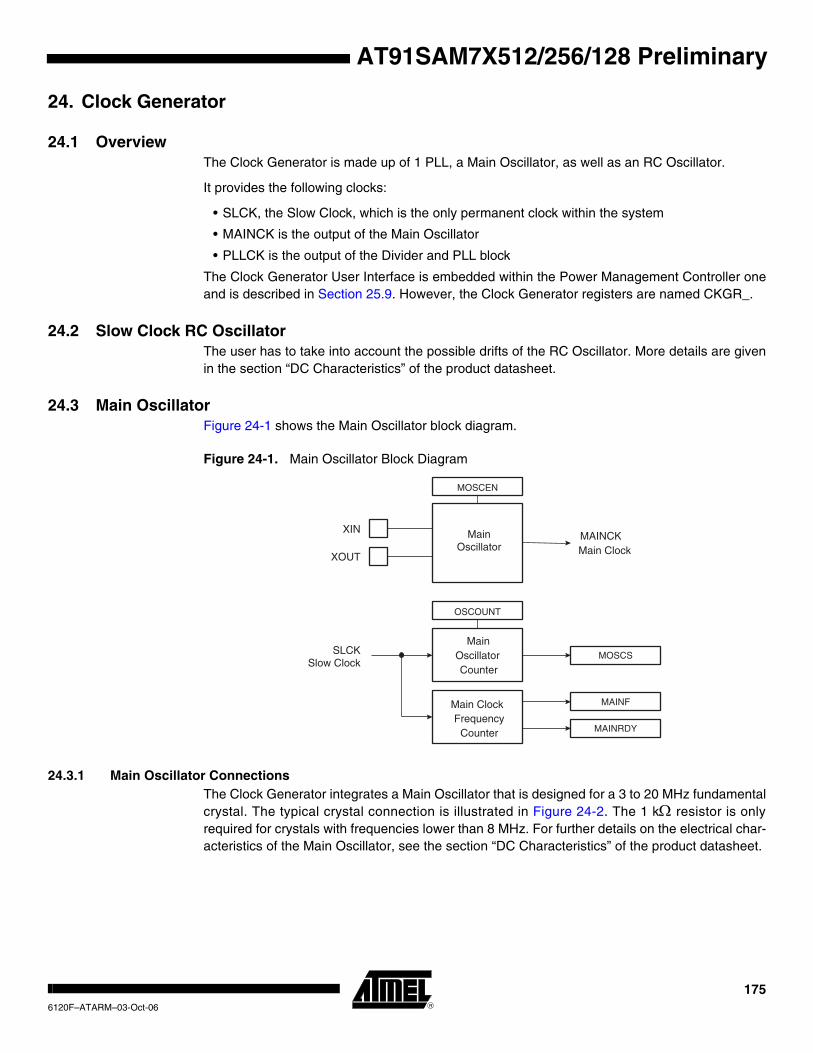
AT91SAM7X512/256/128 Preliminary
24. Clock Generator
24.1 OverviewThe Clock Generator is made up of 1 PLL, a Main Oscillator, as well as an RC Oscillator.
It provides the following clocks:
• SLCK, the Slow Clock, which is the only permanent clock within the system
• MAINCK is the output of the Main Oscillator
• PLLCK is the output of the Divider and PLL block
The Clock Generator User Interface is embedded within the Power Management Controller one and is described in Section 25.9. However, the Clock Generator registers are named CKGR_.
24.2 Slow Clock RC OscillatorThe user has to take into account the possible drifts of the RC Oscillator. More details are given in the section “DC Characteristics” of the product datasheet.
24.3 Main Oscillator Figure 24-1 shows the Main Oscillator block diagram.
Figure 24-1. Main Oscillator Block Diagram
24.3.1 Main Oscillator ConnectionsThe Clock Generator integrates a Main Oscillator that is designed for a 3 to 20 MHz fundamental crystal. The typical crystal connection is illustrated in Figure 24-2. The 1 kΩ resistor is only required for crystals with frequencies lower than 8 MHz. For further details on the electrical char-acteristics of the Main Oscillator, see the section “DC Characteristics” of the product datasheet.
XIN
XOUT
MOSCEN
MainOscillatorCounter
OSCOUNT
MOSCS
MAINCKMain Clock
Main ClockFrequency
Counter
MAINF
MAINRDY
SLCKSlow Clock
MainOscillator
1756120F–ATARM–03-Oct-06

Figure 24-2. Typical Crystal Connection
24.3.2 Main Oscillator Startup TimeThe startup time of the Main Oscillator is given in the DC Characteristics section of the product datasheet. The startup time depends on the crystal frequency and decreases when the fre-quency rises.
24.3.3 Main Oscillator ControlTo minimize the power required to start up the system, the main oscillator is disabled after reset and slow clock is selected.
The software enables or disables the main oscillator so as to reduce power consumption by clearing the MOSCEN bit in the Main Oscillator Register (CKGR_MOR).
When disabling the main oscillator by clearing the MOSCEN bit in CKGR_MOR, the MOSCS bit in PMC_SR is automatically cleared, indicating the main clock is off.
When enabling the main oscillator, the user must initiate the main oscillator counter with a value corresponding to the startup time of the oscillator. This startup time depends on the crystal fre-quency connected to the main oscillator.
When the MOSCEN bit and the OSCOUNT are written in CKGR_MOR to enable the main oscil-lator, the MOSCS bit in PMC_SR (Status Register) is cleared and the counter starts counting down on the slow clock divided by 8 from the OSCOUNT value. Since the OSCOUNT value is coded with 8 bits, the maximum startup time is about 62 ms.
When the counter reaches 0, the MOSCS bit is set, indicating that the main clock is valid. Set-ting the MOSCS bit in PMC_IMR can trigger an interrupt to the processor.
24.3.4 Main Clock Frequency CounterThe Main Oscillator features a Main Clock frequency counter that provides the quartz frequency connected to the Main Oscillator. Generally, this value is known by the system designer; how-ever, it is useful for the boot program to configure the device with the correct clock speed, independently of the application.
The Main Clock frequency counter starts incrementing at the Main Clock speed after the next ris-ing edge of the Slow Clock as soon as the Main Oscillator is stable, i.e., as soon as the MOSCS bit is set. Then, at the 16th falling edge of Slow Clock, the MAINRDY bit in CKGR_MCFR (Main Clock Frequency Register) is set and the counter stops counting. Its value can be read in the MAINF field of CKGR_MCFR and gives the number of Main Clock cycles during 16 periods of Slow Clock, so that the frequency of the crystal connected on the Main Oscillator can be determined.
1K
XIN XOUT GND
CL2CL1
1766120F–ATARM–03-Oct-06
AT91SAM7X512/256/128 Preliminary

AT91SAM7X512/256/128 Preliminary
24.3.5 Main Oscillator BypassThe user can input a clock on the device instead of connecting a crystal. In this case, the user has to provide the external clock signal on the XIN pin. The input characteristics of the XIN pin under these conditions are given in the product electrical characteristics section. The program-mer has to be sure to set the OSCBYPASS bit to 1 and the MOSCEN bit to 0 in the Main OSC register (CKGR_MOR) for the external clock to operate properly.
24.4 Divider and PLL BlockThe PLL embeds an input divider to increase the accuracy of the resulting clock signals. How-ever, the user must respect the PLL minimum input frequency when programming the divider.
Figure 24-3 shows the block diagram of the divider and PLL block.
Figure 24-3. Divider and PLL Block Diagram
24.4.1 PLL FilterThe PLL requires connection to an external second-order filter through the PLLRC pin. Figure 24-4 shows a schematic of these filters.
Figure 24-4. PLL Capacitors and Resistors
Values of R, C1 and C2 to be connected to the PLLRC pin must be calculated as a function of the PLL input frequency, the PLL output frequency and the phase margin. A trade-off has to be found between output signal overshoot and startup time.
24.4.2 Divider and Phase Lock Loop ProgrammingThe divider can be set between 1 and 255 in steps of 1. When a divider field (DIV) is set to 0, the output of the corresponding divider and the PLL output is a continuous signal at level 0. On reset, each DIV field is set to 0, thus the corresponding PLL input clock is set to 0.
Divider
PLLRC
DIV
PLL
MUL
PLLCOUNT
LOCK
OUT
SLCK
MAINCK PLLCK
PLLCounter
GND
C1
C2
PLLPLLRC
R
1776120F–ATARM–03-Oct-06

The PLL allows multiplication of the divider’s outputs. The PLL clock signal has a frequency that depends on the respective source signal frequency and on the parameters DIV and MUL. The factor applied to the source signal frequency is (MUL + 1)/DIV. When MUL is written to 0, the corresponding PLL is disabled and its power consumption is saved. Re-enabling the PLL can be performed by writing a value higher than 0 in the MUL field.
Whenever the PLL is re-enabled or one of its parameters is changed, the LOCK bit in PMC_SR is automatically cleared. The values written in the PLLCOUNT field in CKGR_PLLR are loaded in the PLL counter. The PLL counter then decrements at the speed of the Slow Clock until it reaches 0. At this time, the LOCK bit is set in PMC_SR and can trigger an interrupt to the pro-cessor. The user has to load the number of Slow Clock cycles required to cover the PLL transient time into the PLLCOUNT field. The transient time depends on the PLL filter. The initial state of the PLL and its target frequency can be calculated using a specific tool provided by Atmel.
1786120F–ATARM–03-Oct-06
AT91SAM7X512/256/128 Preliminary

AT91SAM7X512/256/128 Preliminary
25. Power Management Controller (PMC)
25.1 DescriptionThe Power Management Controller (PMC) optimizes power consumption by controlling all sys-tem and user peripheral clocks. The PMC enables/disables the clock inputs to many of the peripherals and the ARM Processor.
The Power Management Controller provides the following clocks:
• MCK, the Master Clock, programmable from a few hundred Hz to the maximum operating frequency of the device. It is available to the modules running permanently, such as the AIC and the Memory Controller.
• Processor Clock (PCK), switched off when entering processor in idle mode.
• Peripheral Clocks, typically MCK, provided to the embedded peripherals (USART, SSC, SPI, TWI, TC, MCI, etc.) and independently controllable. In order to reduce the number of clock names in a product, the Peripheral Clocks are named MCK in the product datasheet.
• UDP Clock (UDPCK), required by USB Device Port operations.
• Programmable Clock Outputs can be selected from the clocks provided by the clock generator and driven on the PCKx pins.
25.2 Master Clock ControllerThe Master Clock Controller provides selection and division of the Master Clock (MCK). MCK is the clock provided to all the peripherals and the memory controller.
The Master Clock is selected from one of the clocks provided by the Clock Generator. Selecting the Slow Clock provides a Slow Clock signal to the whole device. Selecting the Main Clock saves power consumption of the PLL.
The Master Clock Controller is made up of a clock selector and a prescaler.
The Master Clock selection is made by writing the CSS field (Clock Source Selection) in PMC_MCKR (Master Clock Register). The prescaler supports the division by a power of 2 of the selected clock between 1 and 64. The PRES field in PMC_MCKR programs the prescaler.
Each time PMC_MCKR is written to define a new Master Clock, the MCKRDY bit is cleared in PMC_SR. It reads 0 until the Master Clock is established. Then, the MCKRDY bit is set and can trigger an interrupt to the processor. This feature is useful when switching from a high-speed clock to a lower one to inform the software when the change is actually done.
Figure 25-1. Master Clock Controller
SLCKMaster Clock
PrescalerMCK
PRESCSS
MAINCK
PLLCK
To the Processor Clock Controller (PCK)
PMC_MCKR PMC_MCKR
1796120F–ATARM–03-Oct-06
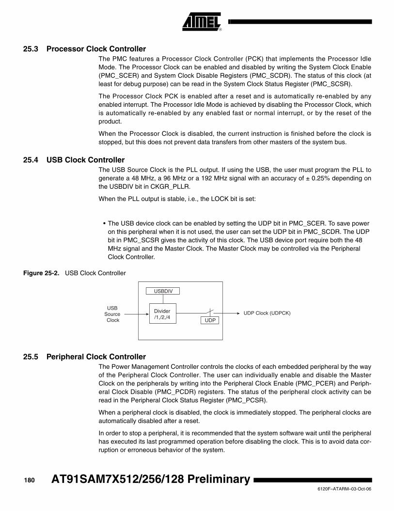
25.3 Processor Clock ControllerThe PMC features a Processor Clock Controller (PCK) that implements the Processor Idle Mode. The Processor Clock can be enabled and disabled by writing the System Clock Enable (PMC_SCER) and System Clock Disable Registers (PMC_SCDR). The status of this clock (at least for debug purpose) can be read in the System Clock Status Register (PMC_SCSR).
The Processor Clock PCK is enabled after a reset and is automatically re-enabled by any enabled interrupt. The Processor Idle Mode is achieved by disabling the Processor Clock, which is automatically re-enabled by any enabled fast or normal interrupt, or by the reset of the product.
When the Processor Clock is disabled, the current instruction is finished before the clock is stopped, but this does not prevent data transfers from other masters of the system bus.
25.4 USB Clock ControllerThe USB Source Clock is the PLL output. If using the USB, the user must program the PLL to generate a 48 MHz, a 96 MHz or a 192 MHz signal with an accuracy of ± 0.25% depending on the USBDIV bit in CKGR_PLLR.
When the PLL output is stable, i.e., the LOCK bit is set:
• The USB device clock can be enabled by setting the UDP bit in PMC_SCER. To save power on this peripheral when it is not used, the user can set the UDP bit in PMC_SCDR. The UDP bit in PMC_SCSR gives the activity of this clock. The USB device port require both the 48 MHz signal and the Master Clock. The Master Clock may be controlled via the Peripheral Clock Controller.
Figure 25-2. USB Clock Controller
25.5 Peripheral Clock ControllerThe Power Management Controller controls the clocks of each embedded peripheral by the way of the Peripheral Clock Controller. The user can individually enable and disable the Master Clock on the peripherals by writing into the Peripheral Clock Enable (PMC_PCER) and Periph-eral Clock Disable (PMC_PCDR) registers. The status of the peripheral clock activity can be read in the Peripheral Clock Status Register (PMC_PCSR).
When a peripheral clock is disabled, the clock is immediately stopped. The peripheral clocks are automatically disabled after a reset.
In order to stop a peripheral, it is recommended that the system software wait until the peripheral has executed its last programmed operation before disabling the clock. This is to avoid data cor-ruption or erroneous behavior of the system.
USB Source Clock
UDP Clock (UDPCK)
UDP
USBDIV
Divider/1,/2,/4
1806120F–ATARM–03-Oct-06
AT91SAM7X512/256/128 Preliminary

AT91SAM7X512/256/128 Preliminary
The bit number within the Peripheral Clock Control registers (PMC_PCER, PMC_PCDR, and PMC_PCSR) is the Peripheral Identifier defined at the product level. Generally, the bit number corresponds to the interrupt source number assigned to the peripheral.
25.6 Programmable Clock Output ControllerThe PMC controls 4 signals to be output on external pins PCKx. Each signal can be indepen-dently programmed via the PMC_PCKx registers.
PCKx can be independently selected between the Slow clock, the PLL output and the main clock by writing the CSS field in PMC_PCKx. Each output signal can also be divided by a power of 2 between 1 and 64 by writing the PRES (Prescaler) field in PMC_PCKx.
Each output signal can be enabled and disabled by writing 1 in the corresponding bit, PCKx of PMC_SCER and PMC_SCDR, respectively. Status of the active programmable output clocks are given in the PCKx bits of PMC_SCSR (System Clock Status Register).
Moreover, like the PCK, a status bit in PMC_SR indicates that the Programmable Clock is actu-ally what has been programmed in the Programmable Clock registers.
As the Programmable Clock Controller does not manage with glitch prevention when switching clocks, it is strongly recommended to disable the Programmable Clock before any configuration change and to re-enable it after the change is actually performed.
25.7 Programming Sequence1. Enabling the Main Oscillator:
The main oscillator is enabled by setting the MOSCEN field in the CKGR_MOR register. In some cases it may be advantageous to define a start-up time. This can be achieved by writ-ing a value in the OSCOUNT field in the CKGR_MOR register.
Once this register has been correctly configured, the user must wait for MOSCS field in the PMC_SR register to be set. This can be done either by polling the status register or by wait-ing the interrupt line to be raised if the associated interrupt to MOSCS has been enabled in the PMC_IER register.
Code Example:
write_register(CKGR_MOR,0x00000701)
Start Up Time = 8 * OSCOUNT / SLCK = 56 Slow Clock Cycles.
So, the main oscillator will be enabled (MOSCS bit set) after 56 Slow Clock Cycles.
2. Checking the Main Oscillator Frequency (Optional):
In some situations the user may need an accurate measure of the main oscillator frequency. This measure can be accomplished via the CKGR_MCFR register.
Once the MAINRDY field is set in CKGR_MCFR register, the user may read the MAINF field in CKGR_MCFR register. This provides the number of main clock cycles within sixteen slow clock cycles.
1816120F–ATARM–03-Oct-06

3. Setting PLL and divider:
All parameters needed to configure PLL and the divider are located in the CKGR_PLLR register.
The DIV field is used to control divider itself. A value between 0 and 255 can be programmed. Divider output is divider input divided by DIV parameter. By default DIV parameter is set to 0 which means that divider is turned off.
The OUT field is used to select the PLL B output frequency range.
The MUL field is the PLL multiplier factor. This parameter can be programmed between 0 and 2047. If MUL is set to 0, PLL will be turned off, otherwise the PLL output frequency is PLL input frequency multiplied by (MUL + 1).
The PLLCOUNT field specifies the number of slow clock cycles before LOCK bit is set in the PMC_SR register after CKGR_PLLR register has been written.
Once the PMC_PLL register has been written, the user must wait for the LOCK bit to be set in the PMC_SR register. This can be done either by polling the status register or by waiting the interrupt line to be raised if the associated interrupt to LOCK has been enabled in the PMC_IER register. All parameters in CKGR_PLLR can be programmed in a single write operation. If at some stage one of the following parameters, MUL, DIV is modified, LOCK bit will go low to indicate that PLL is not ready yet. When PLL is locked, LOCK will be set again. The user is constrained to wait for LOCK bit to be set before using the PLL output clock.
The USBDIV field is used to control the additional divider by 1, 2 or 4, which generates the USB clock(s).
Code Example:
write_register(CKGR_PLLR,0x00040805)
If PLL and divider are enabled, the PLL input clock is the main clock. PLL output clock is PLL input clock multiplied by 5. Once CKGR_PLLR has been written, LOCK bit will be set after eight slow clock cycles.
4. Selection of Master Clock and Processor Clock
The Master Clock and the Processor Clock are configurable via the PMC_MCKR register.
The CSS field is used to select the Master Clock divider source. By default, the selected clock source is slow clock.
The PRES field is used to control the Master Clock prescaler. The user can choose between different values (1, 2, 4, 8, 16, 32, 64). Master Clock output is prescaler input divided by PRES parameter. By default, PRES parameter is set to 1 which means that master clock is equal to slow clock.
Once the PMC_MCKR register has been written, the user must wait for the MCKRDY bit to be set in the PMC_SR register. This can be done either by polling the status register or by waiting for the interrupt line to be raised if the associated interrupt to MCKRDY has been enabled in the PMC_IER register.
The PMC_MCKR register must not be programmed in a single write operation. The preferred programming sequence for the PMC_MCKR register is as follows:
1826120F–ATARM–03-Oct-06
AT91SAM7X512/256/128 Preliminary
AT91SAM7X512/256/128 Preliminary
• If a new value for CSS field corresponds to PLL Clock,
– Program the PRES field in the PMC_MCKR register.
– Wait for the MCKRDY bit to be set in the PMC_SR register.
– Program the CSS field in the PMC_MCKR register.
– Wait for the MCKRDY bit to be set in the PMC_SR register.
• If a new value for CSS field corresponds to Main Clock or Slow Clock,
– Program the CSS field in the PMC_MCKR register.
– Wait for the MCKRDY bit to be set in the PMC_SR register.
– Program the PRES field in the PMC_MCKR register.
– Wait for the MCKRDY bit to be set in the PMC_SR register.
If at some stage one of the following parameters, CSS or PRES, is modified, the MCKRDY bit will go low to indicate that the Master Clock and the Processor Clock are not ready yet. The user must wait for MCKRDY bit to be set again before using the Master and Processor Clocks.
Note: IF PLLx clock was selected as the Master Clock and the user decides to modify it by writing in CKGR_PLLR, the MCKRDY flag will go low while PLL is unlocked. Once PLL is locked again, LOCK goes high and MCKRDY is set. While PLL is unlocked, the Master Clock selection is automatically changed to Main Clock. For fur-ther information, see Section 25.8.2. ”Clock Switching Waveforms” on page 185.
Code Example:
write_register(PMC_MCKR,0x00000001)
wait (MCKRDY=1)
write_register(PMC_MCKR,0x00000011)
wait (MCKRDY=1)
The Master Clock is main clock divided by 16.
The Processor Clock is the Master Clock.
5. Selection of Programmable clocks
Programmable clocks are controlled via registers; PMC_SCER, PMC_SCDR and PMC_SCSR.
Programmable clocks can be enabled and/or disabled via the PMC_SCER and PMC_SCDR registers. Depending on the system used, 4 Programmable clocks can be enabled or dis-abled. The PMC_SCSR provides a clear indication as to which Programmable clock is enabled. By default all Programmable clocks are disabled.
PMC_PCKx registers are used to configure Programmable clocks.
The CSS field is used to select the Programmable clock divider source. Four clock options are available: main clock, slow clock, PLLCK. By default, the clock source selected is slow clock.
The PRES field is used to control the Programmable clock prescaler. It is possible to choose between different values (1, 2, 4, 8, 16, 32, 64). Programmable clock output is prescaler input
1836120F–ATARM–03-Oct-06
divided by PRES parameter. By default, the PRES parameter is set to 1 which means that master clock is equal to slow clock.
Once the PMC_PCKx register has been programmed, The corresponding Programmable clock must be enabled and the user is constrained to wait for the PCKRDYx bit to be set in the PMC_SR register. This can be done either by polling the status register or by waiting the interrupt line to be raised if the associated interrupt to PCKRDYx has been enabled in the PMC_IER register. All parameters in PMC_PCKx can be programmed in a single write operation.
If the CSS and PRES parameters are to be modified, the corresponding Programmable clock must be disabled first. The parameters can then be modified. Once this has been done, the user must re-enable the Programmable clock and wait for the PCKRDYx bit to be set.
Code Example:
write_register(PMC_PCK0,0x00000015)
Programmable clock 0 is main clock divided by 32.
6. Enabling Peripheral Clocks
Once all of the previous steps have been completed, the peripheral clocks can be enabled and/or disabled via registers PMC_PCER and PMC_PCDR.
Depending on the system used, 15 peripheral clocks can be enabled or disabled. The PMC_PCSR provides a clear view as to which peripheral clock is enabled.
Note: Each enabled peripheral clock corresponds to Master Clock.
Code Examples:
write_register(PMC_PCER,0x00000110)
Peripheral clocks 4 and 8 are enabled.
write_register(PMC_PCDR,0x00000010)
Peripheral clock 4 is disabled.
1846120F–ATARM–03-Oct-06
AT91SAM7X512/256/128 Preliminary
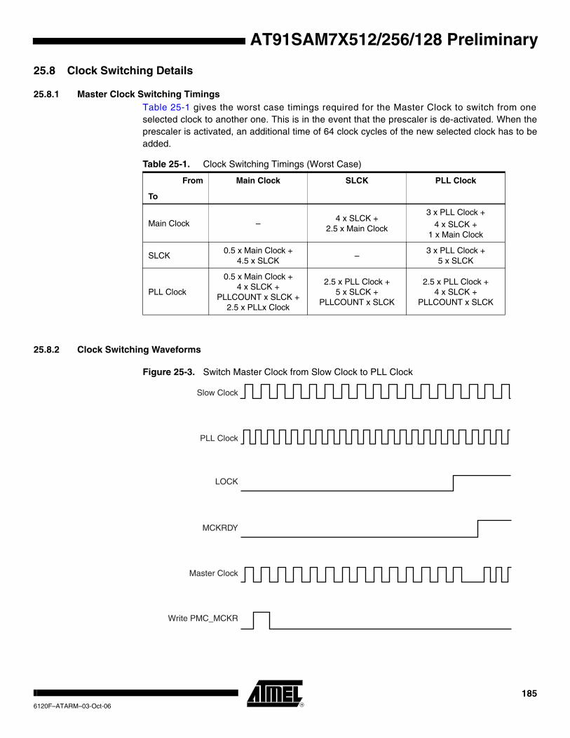
AT91SAM7X512/256/128 Preliminary
25.8 Clock Switching Details
25.8.1 Master Clock Switching TimingsTable 25-1 gives the worst case timings required for the Master Clock to switch from one selected clock to another one. This is in the event that the prescaler is de-activated. When the prescaler is activated, an additional time of 64 clock cycles of the new selected clock has to be added.
25.8.2 Clock Switching Waveforms
Figure 25-3. Switch Master Clock from Slow Clock to PLL Clock
Table 25-1. Clock Switching Timings (Worst Case)
From Main Clock SLCK PLL Clock
To
Main Clock –4 x SLCK +
2.5 x Main Clock
3 x PLL Clock +
4 x SLCK +1 x Main Clock
SLCK0.5 x Main Clock +
4.5 x SLCK–
3 x PLL Clock +5 x SLCK
PLL Clock
0.5 x Main Clock +4 x SLCK +
PLLCOUNT x SLCK +2.5 x PLLx Clock
2.5 x PLL Clock +5 x SLCK +
PLLCOUNT x SLCK
2.5 x PLL Clock +4 x SLCK +
PLLCOUNT x SLCK
Slow Clock
LOCK
MCKRDY
Master Clock
Write PMC_MCKR
PLL Clock
1856120F–ATARM–03-Oct-06
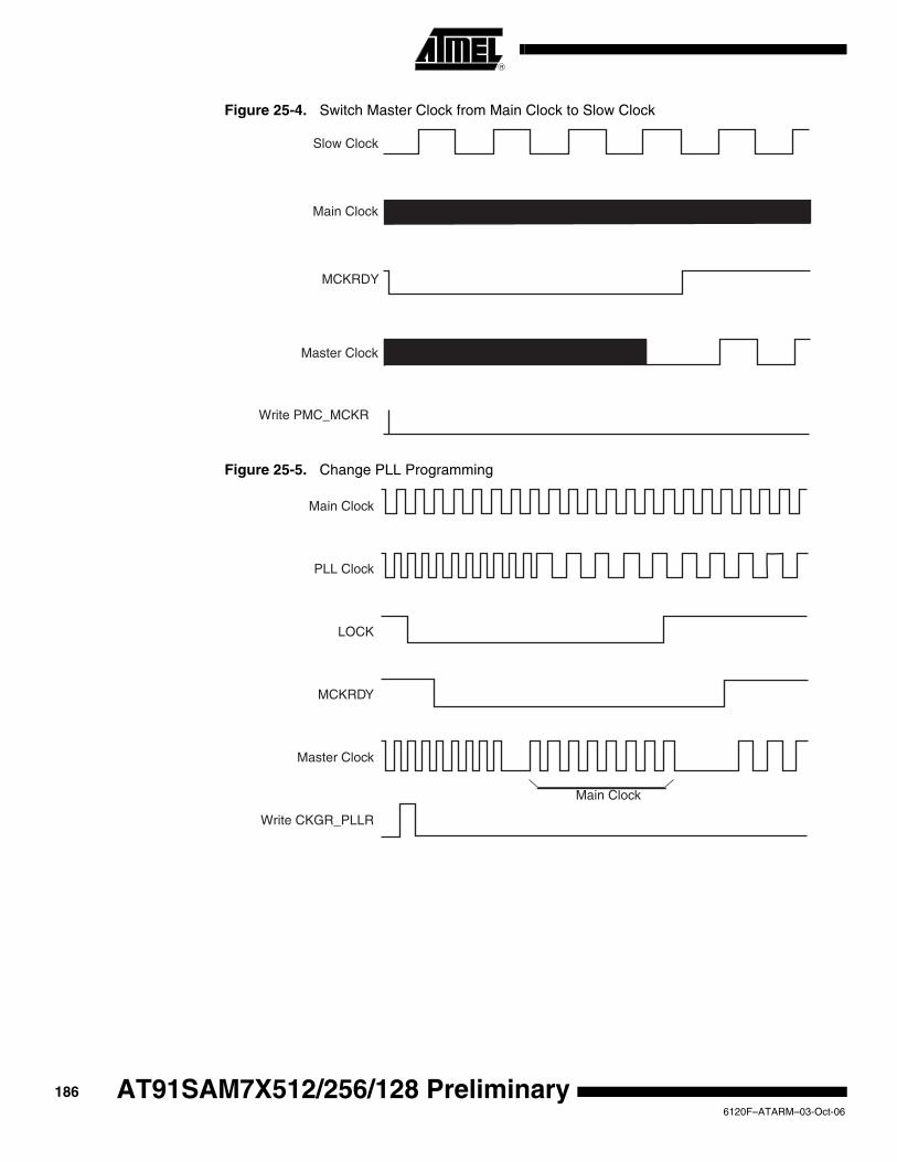
Figure 25-4. Switch Master Clock from Main Clock to Slow Clock
Figure 25-5. Change PLL Programming
Slow Clock
Main Clock
MCKRDY
Master Clock
Write PMC_MCKR
Main Clock
Main Clock
PLL Clock
LOCK
MCKRDY
Master Clock
Write CKGR_PLLR
1866120F–ATARM–03-Oct-06
AT91SAM7X512/256/128 Preliminary
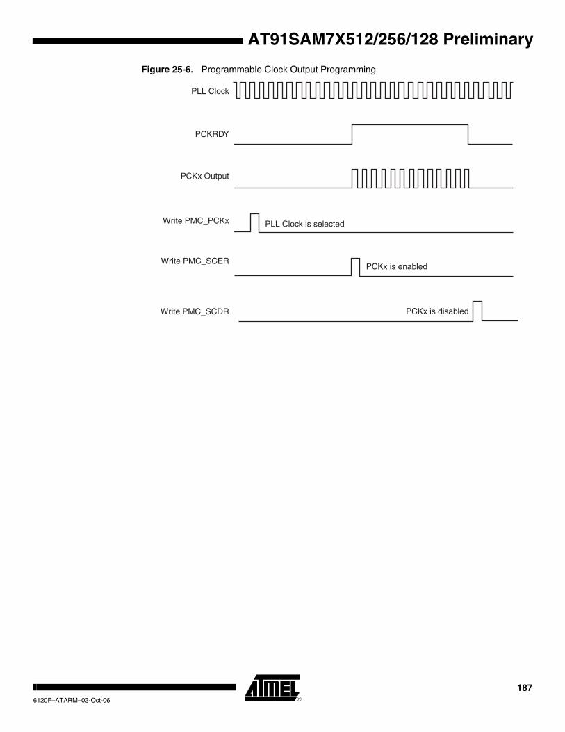
AT91SAM7X512/256/128 Preliminary
Figure 25-6. Programmable Clock Output Programming
PLL Clock
PCKRDY
PCKx Output
Write PMC_PCKx
Write PMC_SCER
Write PMC_SCDR PCKx is disabled
PCKx is enabled
PLL Clock is selected
1876120F–ATARM–03-Oct-06
25.9 Power Management Controller (PMC) User Interface
Table 25-2. Register Mapping
Offset Register Name Access Reset Value
0x0000 System Clock Enable Register PMC_SCER Write-only –
0x0004 System Clock Disable Register PMC_SCDR Write-only –
0x0008 System Clock Status Register PMC _SCSR Read-only 0x01
0x000C Reserved – – –
0x0010 Peripheral Clock Enable Register PMC _PCER Write-only –
0x0014 Peripheral Clock Disable Register PMC_PCDR Write-only –
0x0018 Peripheral Clock Status Register PMC_PCSR Read-only 0x0
0x001C Reserved – – –
0x0020 Main Oscillator Register CKGR_MOR Read/Write 0x0
0x0024 Main Clock Frequency Register CKGR_MCFR Read-only 0x0
0x0028 Reserved – – –
0x002C PLL Register CKGR_PLLR Read/Write 0x3F00
0x0030 Master Clock Register PMC_MCKR Read/Write 0x0
0x0038 Reserved – – –
0x003C Reserved – – –
0x0040 Programmable Clock 0 Register PMC_PCK0 Read/Write 0x0
0x0044 Programmable Clock 1 Register PMC_PCK1 Read/Write 0x0
... ... ... ... ...
0x0060 Interrupt Enable Register PMC_IER Write-only --
0x0064 Interrupt Disable Register PMC_IDR Write-only --
0x0068 Status Register PMC_SR Read-only 0x08
0x006C Interrupt Mask Register PMC_IMR Read-only 0x0
0x0070 - 0x007C Reserved – – –
1886120F–ATARM–03-Oct-06
AT91SAM7X512/256/128 Preliminary

AT91SAM7X512/256/128 Preliminary
25.9.1 PMC System Clock Enable RegisterRegister Name: PMC_SCER
Access Type: Write-only
• PCK: Processor Clock Enable0 = No effect.
1 = Enables the Processor clock.
• UDP: USB Device Port Clock Enable0 = No effect.
1 = Enables the 48 MHz clock of the USB Device Port.
• PCKx: Programmable Clock x Output Enable0 = No effect.
1 = Enables the corresponding Programmable Clock output.
31 30 29 28 27 26 25 24
– – – – – – – –
23 22 21 20 19 18 17 16
– – – – – – – –
15 14 13 12 11 10 9 8
– – – – PCK3 PCK2 PCK1 PCK0
7 6 5 4 3 2 1 0
UDP – – – – – – PCK
1896120F–ATARM–03-Oct-06
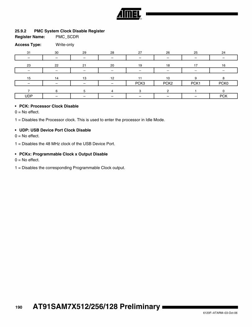
25.9.2 PMC System Clock Disable Register Register Name: PMC_SCDR
Access Type: Write-only
• PCK: Processor Clock Disable0 = No effect.
1 = Disables the Processor clock. This is used to enter the processor in Idle Mode.
• UDP: USB Device Port Clock Disable0 = No effect.
1 = Disables the 48 MHz clock of the USB Device Port.
• PCKx: Programmable Clock x Output Disable0 = No effect.
1 = Disables the corresponding Programmable Clock output.
31 30 29 28 27 26 25 24
– – – – – – – –
23 22 21 20 19 18 17 16
– – – – – – – –
15 14 13 12 11 10 9 8
– – – – PCK3 PCK2 PCK1 PCK0
7 6 5 4 3 2 1 0
UDP – – – – – – PCK
1906120F–ATARM–03-Oct-06
AT91SAM7X512/256/128 Preliminary
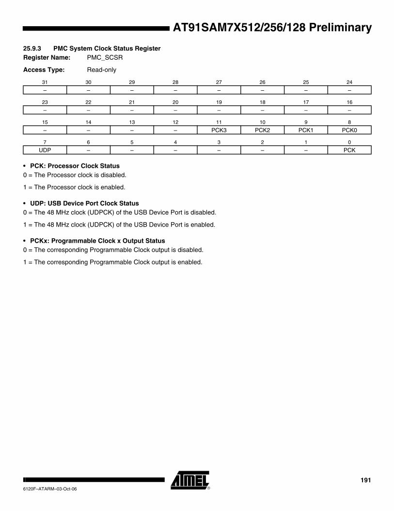
AT91SAM7X512/256/128 Preliminary
25.9.3 PMC System Clock Status Register Register Name: PMC_SCSR
Access Type: Read-only
• PCK: Processor Clock Status0 = The Processor clock is disabled.
1 = The Processor clock is enabled.
• UDP: USB Device Port Clock Status 0 = The 48 MHz clock (UDPCK) of the USB Device Port is disabled.
1 = The 48 MHz clock (UDPCK) of the USB Device Port is enabled.
• PCKx: Programmable Clock x Output Status0 = The corresponding Programmable Clock output is disabled.
1 = The corresponding Programmable Clock output is enabled.
31 30 29 28 27 26 25 24
– – – – – – – –
23 22 21 20 19 18 17 16
– – – – – – – –
15 14 13 12 11 10 9 8
– – – – PCK3 PCK2 PCK1 PCK0
7 6 5 4 3 2 1 0
UDP – – – – – – PCK
1916120F–ATARM–03-Oct-06

25.9.4 PMC Peripheral Clock Enable RegisterRegister Name: PMC_PCER
Access Type: Write-only
• PIDx: Peripheral Clock x Enable0 = No effect.
1 = Enables the corresponding peripheral clock.
Note: PID2 to PID31 refer to identifiers as defined in the section “Peripheral Identifiers” in the product datasheet.
Note: Programming the control bits of the Peripheral ID that are not implemented has no effect on the behavior of the PMC.
25.9.5 PMC Peripheral Clock Disable RegisterRegister Name: PMC_PCDR
Access Type: Write-only
• PIDx: Peripheral Clock x Disable 0 = No effect.
1 = Disables the corresponding peripheral clock.
Note: PID2 to PID31 refer to identifiers as defined in the section “Peripheral Identifiers” in the product datasheet.
31 30 29 28 27 26 25 24
PID31 PID30 PID29 PID28 PID27 PID26 PID25 PID24
23 22 21 20 19 18 17 16
PID23 PID22 PID21 PID20 PID19 PID18 PID17 PID16
15 14 13 12 11 10 9 8
PID15 PID14 PID13 PID12 PID11 PID10 PID9 PID8
7 6 5 4 3 2 1 0
PID7 PID6 PID5 PID4 PID3 PID2 - -
31 30 29 28 27 26 25 24
PID31 PID30 PID29 PID28 PID27 PID26 PID25 PID24
23 22 21 20 19 18 17 16
PID23 PID22 PID21 PID20 PID19 PID18 PID17 PID16
15 14 13 12 11 10 9 8
PID15 PID14 PID13 PID12 PID11 PID10 PID9 PID8
7 6 5 4 3 2 1 0
PID7 PID6 PID5 PID4 PID3 PID2 - -
1926120F–ATARM–03-Oct-06
AT91SAM7X512/256/128 Preliminary
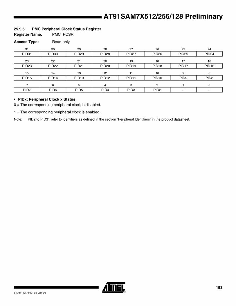
AT91SAM7X512/256/128 Preliminary
25.9.6 PMC Peripheral Clock Status RegisterRegister Name: PMC_PCSR
Access Type: Read-only
• PIDx: Peripheral Clock x Status0 = The corresponding peripheral clock is disabled.
1 = The corresponding peripheral clock is enabled.
Note: PID2 to PID31 refer to identifiers as defined in the section “Peripheral Identifiers” in the product datasheet.
31 30 29 28 27 26 25 24
PID31 PID30 PID29 PID28 PID27 PID26 PID25 PID24
23 22 21 20 19 18 17 16
PID23 PID22 PID21 PID20 PID19 PID18 PID17 PID16
15 14 13 12 11 10 9 8
PID15 PID14 PID13 PID12 PID11 PID10 PID9 PID8
7 6 5 4 3 2 1 0
PID7 PID6 PID5 PID4 PID3 PID2 – –
1936120F–ATARM–03-Oct-06

25.9.7 PMC Clock Generator Main Oscillator RegisterRegister Name: CKGR_MOR
Access Type: Read/Write
• MOSCEN: Main Oscillator EnableA crystal must be connected between XIN and XOUT.
0 = The Main Oscillator is disabled.
1 = The Main Oscillator is enabled. OSCBYPASS must be set to 0.
When MOSCEN is set, the MOSCS flag is set once the Main Oscillator startup time is achieved.
• OSCBYPASS: Oscillator Bypass0 = No effect.
1 = The Main Oscillator is bypassed. MOSCEN must be set to 0. An external clock must be connected on XIN.
When OSCBYPASS is set, the MOSCS flag in PMC_SR is automatically set.
Clearing MOSCEN and OSCBYPASS bits allows resetting the MOSCS flag.
• OSCOUNT: Main Oscillator Start-up TimeSpecifies the number of Slow Clock cycles multiplied by 8 for the Main Oscillator start-up time.
31 30 29 28 27 26 25 24– – – – – – – –
23 22 21 20 19 18 17 16
– – – – – – – –
15 14 13 12 11 10 9 8
OSCOUNT
7 6 5 4 3 2 1 0
– – – – – – OSCBYPASS MOSCEN
1946120F–ATARM–03-Oct-06
AT91SAM7X512/256/128 Preliminary
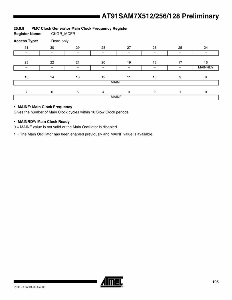
AT91SAM7X512/256/128 Preliminary
25.9.8 PMC Clock Generator Main Clock Frequency Register Register Name: CKGR_MCFR
Access Type: Read-only
• MAINF: Main Clock FrequencyGives the number of Main Clock cycles within 16 Slow Clock periods.
• MAINRDY: Main Clock Ready0 = MAINF value is not valid or the Main Oscillator is disabled.
1 = The Main Oscillator has been enabled previously and MAINF value is available.
31 30 29 28 27 26 25 24– – – – – – – –
23 22 21 20 19 18 17 16
– – – – – – – MAINRDY
15 14 13 12 11 10 9 8
MAINF
7 6 5 4 3 2 1 0
MAINF
1956120F–ATARM–03-Oct-06

25.9.9 PMC Clock Generator PLL Register Register Name: CKGR_PLLR
Access Type: Read/Write
Possible limitations on PLL input frequencies and multiplier factors should be checked before using the PMC.
• DIV: Divider
• PLLCOUNT: PLL CounterSpecifies the number of slow clock cycles before the LOCK bit is set in PMC_SR after CKGR_PLLR is written.
• OUT: PLL Clock Frequency RangeRefer to “PLL Characteristics” in the Electrical Characteristics section of the product datasheet.
• MUL: PLL Multiplier0 = The PLL is deactivated.
1 up to 2047 = The PLL Clock frequency is the PLL input frequency multiplied by MUL+ 1.
• USBDIV: Divider for USB Clock
31 30 29 28 27 26 25 24– – USBDIV – MUL
23 22 21 20 19 18 17 16
MUL
15 14 13 12 11 10 9 8
OUT PLLCOUNT
7 6 5 4 3 2 1 0
DIV
DIV Divider Selected
0 Divider output is 0
1 Divider is bypassed
2 - 255 Divider output is the selected clock divided by DIV.
USBDIV Divider for USB Clock(s)
0 0 Divider output is PLL clock output.
0 1 Divider output is PLL clock output divided by 2.
1 0 Divider output is PLL clock output divided by 4.
1 1 Reserved.
1966120F–ATARM–03-Oct-06
AT91SAM7X512/256/128 Preliminary
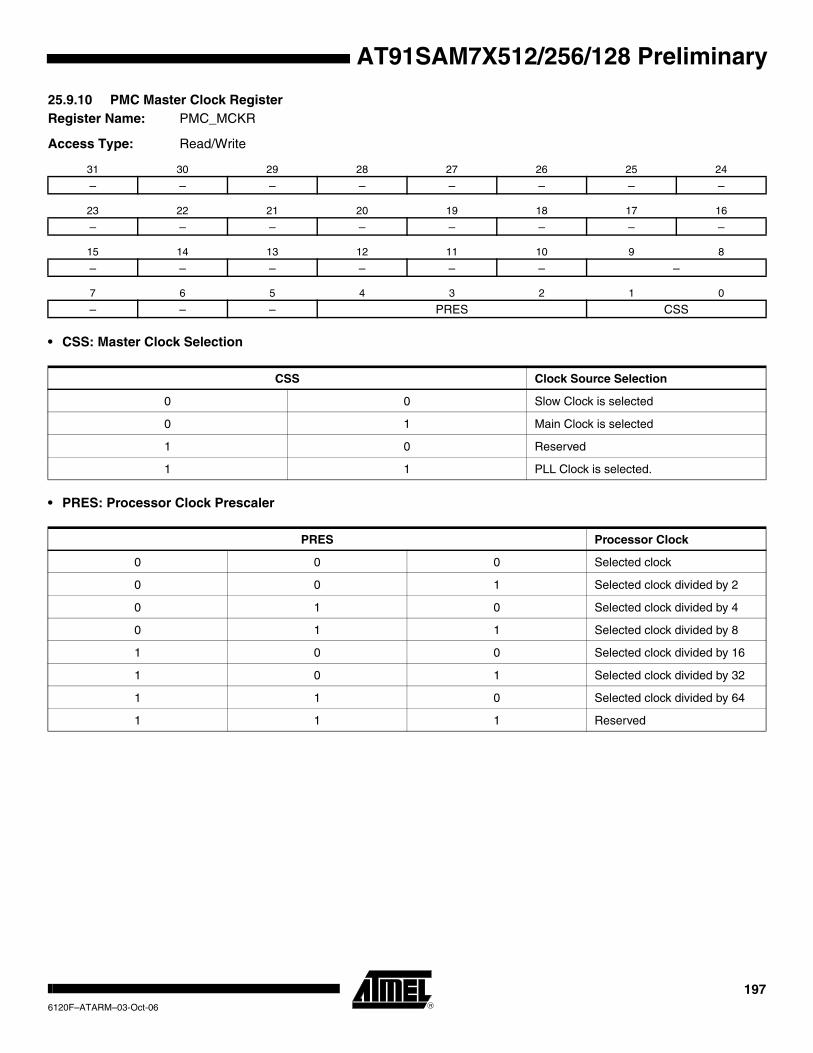
AT91SAM7X512/256/128 Preliminary
25.9.10 PMC Master Clock RegisterRegister Name: PMC_MCKR
Access Type: Read/Write
• CSS: Master Clock Selection
• PRES: Processor Clock Prescaler
31 30 29 28 27 26 25 24
– – – – – – – –
23 22 21 20 19 18 17 16
– – – – – – – –
15 14 13 12 11 10 9 8
– – – – – – –
7 6 5 4 3 2 1 0
– – – PRES CSS
CSS Clock Source Selection
0 0 Slow Clock is selected
0 1 Main Clock is selected
1 0 Reserved
1 1 PLL Clock is selected.
PRES Processor Clock
0 0 0 Selected clock
0 0 1 Selected clock divided by 2
0 1 0 Selected clock divided by 4
0 1 1 Selected clock divided by 8
1 0 0 Selected clock divided by 16
1 0 1 Selected clock divided by 32
1 1 0 Selected clock divided by 64
1 1 1 Reserved
1976120F–ATARM–03-Oct-06

25.9.11 PMC Programmable Clock RegisterRegister Name: PMC_PCKx
Access Type: Read/Write
• CSS: Master Clock Selection
• PRES: Programmable Clock Prescaler
31 30 29 28 27 26 25 24
– – – – – – – –
23 22 21 20 19 18 17 16
– – – – – – – –
15 14 13 12 11 10 9 8
– – – – – – – –
7 6 5 4 3 2 1 0
– – – PRES CSS
CSS Clock Source Selection
0 0 Slow Clock is selected
0 1 Main Clock is selected
1 0 Reserved
1 1 PLL Clock is selected
PRES Programmable Clock
0 0 0 Selected clock
0 0 1 Selected clock divided by 2
0 1 0 Selected clock divided by 4
0 1 1 Selected clock divided by 8
1 0 0 Selected clock divided by 16
1 0 1 Selected clock divided by 32
1 1 0 Selected clock divided by 64
1 1 1 Reserved
1986120F–ATARM–03-Oct-06
AT91SAM7X512/256/128 Preliminary

AT91SAM7X512/256/128 Preliminary
25.9.12 PMC Interrupt Enable RegisterRegister Name: PMC_IER
Access Type: Write-only
• MOSCS: Main Oscillator Status Interrupt Enable
• LOCK: PLL Lock Interrupt Enable
• MCKRDY: Master Clock Ready Interrupt Enable
• PCKRDYx: Programmable Clock Ready x Interrupt Enable0 = No effect.
1 = Enables the corresponding interrupt.
31 30 29 28 27 26 25 24
– – – – – – – –
23 22 21 20 19 18 17 16
– – – – – – – –
15 14 13 12 11 10 9 8
– – – – PCKRDY3 PCKRDY2 PCKRDY1 PCKRDY0
7 6 5 4 3 2 1 0
– – – – MCKRDY LOCK – MOSCS
1996120F–ATARM–03-Oct-06

25.9.13 PMC Interrupt Disable RegisterRegister Name: PMC_IDR
Access Type: Write-only
• MOSCS: Main Oscillator Status Interrupt Disable
• LOCK: PLL Lock Interrupt Disable
• MCKRDY: Master Clock Ready Interrupt Disable
• PCKRDYx: Programmable Clock Ready x Interrupt Disable0 = No effect.
1 = Disables the corresponding interrupt.
31 30 29 28 27 26 25 24
– – – – – – – –
23 22 21 20 19 18 17 16
– – – – – – – –
15 14 13 12 11 10 9 8
– – – – PCKRDY3 PCKRDY2 PCKRDY1 PCKRDY0
7 6 5 4 3 2 1 0
– – – – MCKRDY LOCK – MOSCS
2006120F–ATARM–03-Oct-06
AT91SAM7X512/256/128 Preliminary

AT91SAM7X512/256/128 Preliminary
25.9.14 PMC Status RegisterRegister Name: PMC_SR
Access Type: Read-only
• MOSCS: MOSCS Flag Status0 = Main oscillator is not stabilized.
1 = Main oscillator is stabilized.
• LOCK: PLL Lock Status0 = PLL is not locked
1 = PLL is locked.
• MCKRDY: Master Clock Status0 = Master Clock is not ready.
1 = Master Clock is ready.
• PCKRDYx: Programmable Clock Ready Status0 = Programmable Clock x is not ready.
1 = Programmable Clock x is ready.
31 30 29 28 27 26 25 24
– – – – – – – –
23 22 21 20 19 18 17 16
– – – – – – – –
15 14 13 12 11 10 9 8
– – – – PCKRDY3 PCKRDY2 PCKRDY1 PCKRDY0
7 6 5 4 3 2 1 0
– – – – MCKRDY LOCK – MOSCS
2016120F–ATARM–03-Oct-06
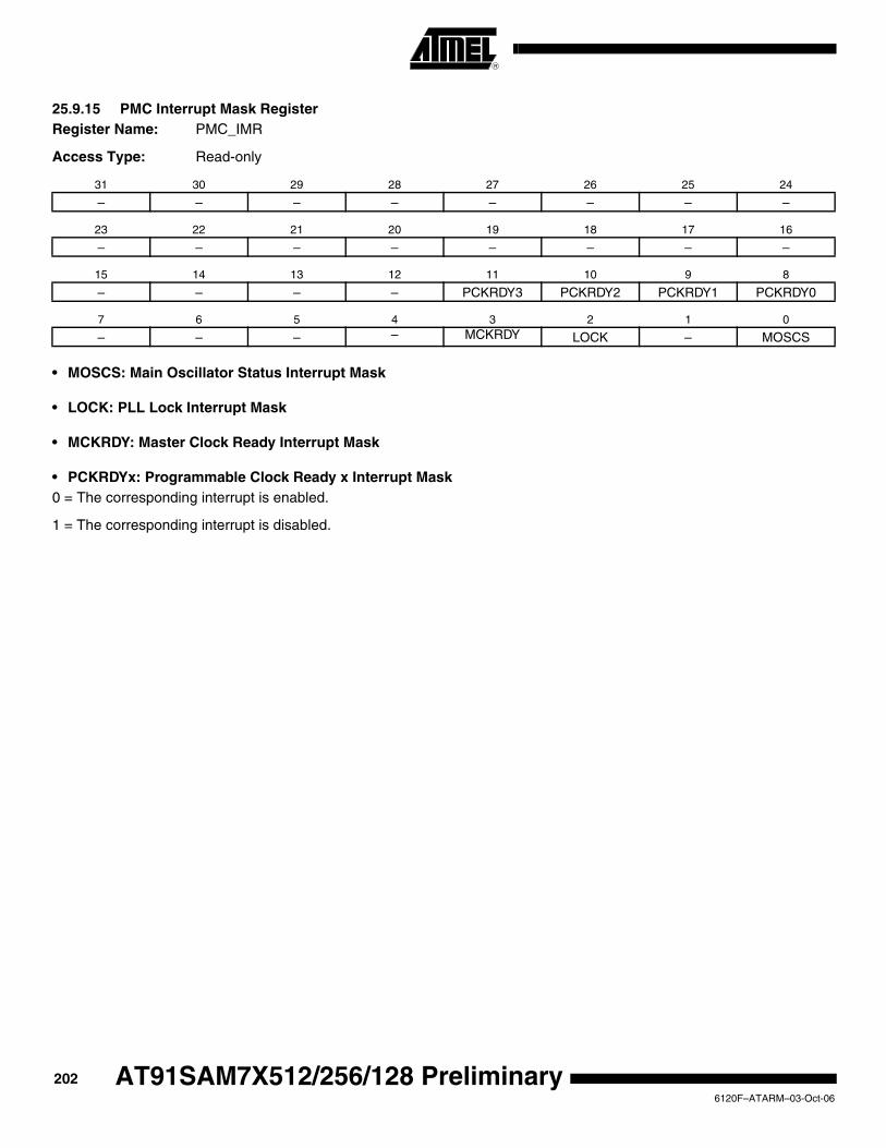
25.9.15 PMC Interrupt Mask RegisterRegister Name: PMC_IMR
Access Type: Read-only
• MOSCS: Main Oscillator Status Interrupt Mask
• LOCK: PLL Lock Interrupt Mask
• MCKRDY: Master Clock Ready Interrupt Mask
• PCKRDYx: Programmable Clock Ready x Interrupt Mask0 = The corresponding interrupt is enabled.
1 = The corresponding interrupt is disabled.
31 30 29 28 27 26 25 24
– – – – – – – –
23 22 21 20 19 18 17 16
– – – – – – – –
15 14 13 12 11 10 9 8
– – – – PCKRDY3 PCKRDY2 PCKRDY1 PCKRDY0
7 6 5 4 3 2 1 0
– – – – MCKRDY LOCK – MOSCS
2026120F–ATARM–03-Oct-06
AT91SAM7X512/256/128 Preliminary
AT91SAM7X512/256/128 Preliminary
26. Debug Unit (DBGU)
26.1 Overview
The Debug Unit provides a single entry point from the processor for access to all the debug capabilities of Atmel’s ARM-based systems.
The Debug Unit features a two-pin UART that can be used for several debug and trace purposes and offers an ideal medium for in-situ programming solutions and debug monitor communica-tions. Moreover, the association with two peripheral data controller channels permits packet handling for these tasks with processor time reduced to a minimum.
The Debug Unit also makes the Debug Communication Channel (DCC) signals provided by the In-circuit Emulator of the ARM processor visible to the software. These signals indicate the sta-tus of the DCC read and write registers and generate an interrupt to the ARM processor, making possible the handling of the DCC under interrupt control.
Chip Identifier registers permit recognition of the device and its revision. These registers inform as to the sizes and types of the on-chip memories, as well as the set of embedded peripherals.
Finally, the Debug Unit features a Force NTRST capability that enables the software to decide whether to prevent access to the system via the In-circuit Emulator. This permits protection of the code, stored in ROM.
2036120F–ATARM–03-Oct-06
26.2 Block Diagram
Figure 26-1. Debug Unit Functional Block Diagram
Figure 26-2. Debug Unit Application Example
Peripheral DMA Controller
Baud RateGenerator
DCCHandler
ICEAccessHandler
Transmit
Receive
Chip ID
InterruptControl
PeripheralBridge
ParallelInput/Output
DTXD
DRXD
PowerManagement
Controller
ARMProcessor
force_ntrst
COMMRX
COMMTX
MCK
nTRST
Power-onReset
dbgu_irq
APB Debug Unit
R
Table 26-1. Debug Unit Pin Description
Pin Name Description Type
DRXD Debug Receive Data Input
DTXD Debug Transmit Data Output
Debug Unit
RS232 Drivers
Programming Tool Trace Console Debug Console
Boot Program Debug Monitor Trace Manager
2046120F–ATARM–03-Oct-06
AT91SAM7X512/256/128 Preliminary

AT91SAM7X512/256/128 Preliminary
26.3 Product Dependencies
26.3.1 I/O Lines
Depending on product integration, the Debug Unit pins may be multiplexed with PIO lines. In this case, the programmer must first configure the corresponding PIO Controller to enable I/O lines operations of the Debug Unit.
26.3.2 Power Management
Depending on product integration, the Debug Unit clock may be controllable through the Power Management Controller. In this case, the programmer must first configure the PMC to enable the Debug Unit clock. Usually, the peripheral identifier used for this purpose is 1.
26.3.3 Interrupt Source
Depending on product integration, the Debug Unit interrupt line is connected to one of the inter-rupt sources of the Advanced Interrupt Controller. Interrupt handling requires programming of the AIC before configuring the Debug Unit. Usually, the Debug Unit interrupt line connects to the interrupt source 1 of the AIC, which may be shared with the real-time clock, the system timer interrupt lines and other system peripheral interrupts, as shown in Figure 26-1. This sharing requires the programmer to determine the source of the interrupt when the source 1 is triggered.
26.4 UART Operations
The Debug Unit operates as a UART, (asynchronous mode only) and supports only 8-bit charac-ter handling (with parity). It has no clock pin.
The Debug Unit's UART is made up of a receiver and a transmitter that operate independently, and a common baud rate generator. Receiver timeout and transmitter time guard are not imple-mented. However, all the implemented features are compatible with those of a standard USART.
26.4.1 Baud Rate Generator
The baud rate generator provides the bit period clock named baud rate clock to both the receiver and the transmitter.
The baud rate clock is the master clock divided by 16 times the value (CD) written in DBGU_BRGR (Baud Rate Generator Register). If DBGU_BRGR is set to 0, the baud rate clock is disabled and the Debug Unit's UART remains inactive. The maximum allowable baud rate is Master Clock divided by 16. The minimum allowable baud rate is Master Clock divided by (16 x 65536).
Baud Rate MCK16 CD×---------------------=
2056120F–ATARM–03-Oct-06
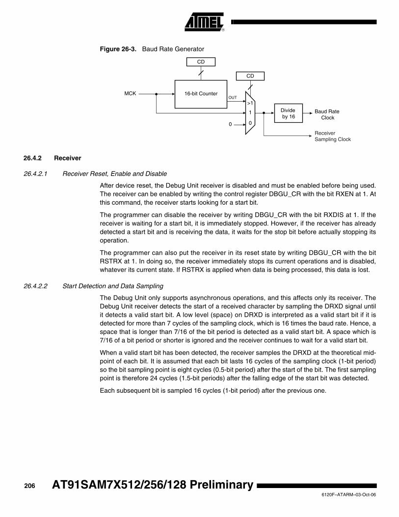
Figure 26-3. Baud Rate Generator
26.4.2 Receiver
26.4.2.1 Receiver Reset, Enable and Disable
After device reset, the Debug Unit receiver is disabled and must be enabled before being used. The receiver can be enabled by writing the control register DBGU_CR with the bit RXEN at 1. At this command, the receiver starts looking for a start bit.
The programmer can disable the receiver by writing DBGU_CR with the bit RXDIS at 1. If the receiver is waiting for a start bit, it is immediately stopped. However, if the receiver has already detected a start bit and is receiving the data, it waits for the stop bit before actually stopping its operation.
The programmer can also put the receiver in its reset state by writing DBGU_CR with the bit RSTRX at 1. In doing so, the receiver immediately stops its current operations and is disabled, whatever its current state. If RSTRX is applied when data is being processed, this data is lost.
26.4.2.2 Start Detection and Data Sampling
The Debug Unit only supports asynchronous operations, and this affects only its receiver. The Debug Unit receiver detects the start of a received character by sampling the DRXD signal until it detects a valid start bit. A low level (space) on DRXD is interpreted as a valid start bit if it is detected for more than 7 cycles of the sampling clock, which is 16 times the baud rate. Hence, a space that is longer than 7/16 of the bit period is detected as a valid start bit. A space which is 7/16 of a bit period or shorter is ignored and the receiver continues to wait for a valid start bit.
When a valid start bit has been detected, the receiver samples the DRXD at the theoretical mid-point of each bit. It is assumed that each bit lasts 16 cycles of the sampling clock (1-bit period) so the bit sampling point is eight cycles (0.5-bit period) after the start of the bit. The first sampling point is therefore 24 cycles (1.5-bit periods) after the falling edge of the start bit was detected.
Each subsequent bit is sampled 16 cycles (1-bit period) after the previous one.
MCK 16-bit Counter
0
Baud Rate Clock
CD
CD
OUT
Divide by 16
0
1
>1
ReceiverSampling Clock
2066120F–ATARM–03-Oct-06
AT91SAM7X512/256/128 Preliminary

AT91SAM7X512/256/128 Preliminary
Figure 26-4. Start Bit Detection
Figure 26-5. Character Reception
26.4.2.3 Receiver Ready
When a complete character is received, it is transferred to the DBGU_RHR and the RXRDY sta-tus bit in DBGU_SR (Status Register) is set. The bit RXRDY is automatically cleared when the receive holding register DBGU_RHR is read.
Figure 26-6. Receiver Ready
26.4.2.4 Receiver Overrun
If DBGU_RHR has not been read by the software (or the Peripheral Data Controller) since the last transfer, the RXRDY bit is still set and a new character is received, the OVRE status bit in DBGU_SR is set. OVRE is cleared when the software writes the control register DBGU_CR with the bit RSTSTA (Reset Status) at 1.
Figure 26-7. Receiver Overrun
Sampling Clock
DRXD
True Start Detection
D0
Baud RateClock
D0 D1 D2 D3 D4 D5 D6 D7
DRXD
True Start DetectionSampling
Parity BitStop Bit
Example: 8-bit, parity enabled 1 stop
1 bit period
0.5 bit period
D0 D1 D2 D3 D4 D5 D6 D7 PS S D0 D1 D2 D3 D4 D5 D6 D7 PDRXD
Read DBGU_RHR
RXRDY
D0 D1 D2 D3 D4 D5 D6 D7 PS S D0 D1 D2 D3 D4 D5 D6 D7 PDRXD
RSTSTA
RXRDY
OVRE
stop stop
2076120F–ATARM–03-Oct-06

26.4.2.5 Parity Error
Each time a character is received, the receiver calculates the parity of the received data bits, in accordance with the field PAR in DBGU_MR. It then compares the result with the received parity bit. If different, the parity error bit PARE in DBGU_SR is set at the same time the RXRDY is set. The parity bit is cleared when the control register DBGU_CR is written with the bit RSTSTA (Reset Status) at 1. If a new character is received before the reset status command is written, the PARE bit remains at 1.
Figure 26-8. Parity Error
26.4.2.6 Receiver Framing Error
When a start bit is detected, it generates a character reception when all the data bits have been sampled. The stop bit is also sampled and when it is detected at 0, the FRAME (Framing Error) bit in DBGU_SR is set at the same time the RXRDY bit is set. The bit FRAME remains high until the control register DBGU_CR is written with the bit RSTSTA at 1.
Figure 26-9. Receiver Framing Error
26.4.3 Transmitter
26.4.3.1 Transmitter Reset, Enable and Disable
After device reset, the Debug Unit transmitter is disabled and it must be enabled before being used. The transmitter is enabled by writing the control register DBGU_CR with the bit TXEN at 1. From this command, the transmitter waits for a character to be written in the Transmit Holding Register DBGU_THR before actually starting the transmission.
The programmer can disable the transmitter by writing DBGU_CR with the bit TXDIS at 1. If the transmitter is not operating, it is immediately stopped. However, if a character is being pro-cessed into the Shift Register and/or a character has been written in the Transmit Holding Register, the characters are completed before the transmitter is actually stopped.
The programmer can also put the transmitter in its reset state by writing the DBGU_CR with the bit RSTTX at 1. This immediately stops the transmitter, whether or not it is processing characters.
stopD0 D1 D2 D3 D4 D5 D6 D7 PSDRXD
RSTSTA
RXRDY
PARE
Wrong Parity Bit
D0 D1 D2 D3 D4 D5 D6 D7 PSDRXD
RSTSTA
RXRDY
FRAME
Stop Bit Detected at 0
stop
2086120F–ATARM–03-Oct-06
AT91SAM7X512/256/128 Preliminary

AT91SAM7X512/256/128 Preliminary
26.4.3.2 Transmit Format
The Debug Unit transmitter drives the pin DTXD at the baud rate clock speed. The line is driven depending on the format defined in the Mode Register and the data stored in the Shift Register. One start bit at level 0, then the 8 data bits, from the lowest to the highest bit, one optional parity bit and one stop bit at 1 are consecutively shifted out as shown on the following figure. The field PARE in the mode register DBGU_MR defines whether or not a parity bit is shifted out. When a parity bit is enabled, it can be selected between an odd parity, an even parity, or a fixed space or mark bit.
Figure 26-10. Character Transmission
26.4.3.3 Transmitter Control
When the transmitter is enabled, the bit TXRDY (Transmitter Ready) is set in the status register DBGU_SR. The transmission starts when the programmer writes in the Transmit Holding Regis-ter DBGU_THR, and after the written character is transferred from DBGU_THR to the Shift Register. The bit TXRDY remains high until a second character is written in DBGU_THR. As soon as the first character is completed, the last character written in DBGU_THR is transferred into the shift register and TXRDY rises again, showing that the holding register is empty.
When both the Shift Register and the DBGU_THR are empty, i.e., all the characters written in DBGU_THR have been processed, the bit TXEMPTY rises after the last stop bit has been completed.
Figure 26-11. Transmitter Control
D0 D1 D2 D3 D4 D5 D6 D7
DTXD
Start Bit
ParityBit
StopBit
Example: Parity enabled
Baud Rate Clock
DBGU_THR
Shift Register
DTXD
TXRDY
TXEMPTY
Data 0 Data 1
Data 0
Data 0
Data 1
Data 1S S PP
Write Data 0in DBGU_THR
Write Data 1in DBGU_THR
stopstop
2096120F–ATARM–03-Oct-06
26.4.4 Peripheral Data Controller
Both the receiver and the transmitter of the Debug Unit's UART are generally connected to a Peripheral Data Controller (PDC) channel.
The peripheral data controller channels are programmed via registers that are mapped within the Debug Unit user interface from the offset 0x100. The status bits are reported in the Debug Unit status register DBGU_SR and can generate an interrupt.
The RXRDY bit triggers the PDC channel data transfer of the receiver. This results in a read of the data in DBGU_RHR. The TXRDY bit triggers the PDC channel data transfer of the transmit-ter. This results in a write of a data in DBGU_THR.
26.4.5 Test Modes
The Debug Unit supports three tests modes. These modes of operation are programmed by using the field CHMODE (Channel Mode) in the mode register DBGU_MR.
The Automatic Echo mode allows bit-by-bit retransmission. When a bit is received on the DRXD line, it is sent to the DTXD line. The transmitter operates normally, but has no effect on the DTXD line.
The Local Loopback mode allows the transmitted characters to be received. DTXD and DRXD pins are not used and the output of the transmitter is internally connected to the input of the receiver. The DRXD pin level has no effect and the DTXD line is held high, as in idle state.
The Remote Loopback mode directly connects the DRXD pin to the DTXD line. The transmitter and the receiver are disabled and have no effect. This mode allows a bit-by-bit retransmission.
2106120F–ATARM–03-Oct-06
AT91SAM7X512/256/128 Preliminary
AT91SAM7X512/256/128 Preliminary
Figure 26-12. Test Modes
26.4.6 Debug Communication Channel Support
The Debug Unit handles the signals COMMRX and COMMTX that come from the Debug Com-munication Channel of the ARM Processor and are driven by the In-circuit Emulator.
The Debug Communication Channel contains two registers that are accessible through the ICE Breaker on the JTAG side and through the coprocessor 0 on the ARM Processor side.
As a reminder, the following instructions are used to read and write the Debug Communication Channel:
MRC p14, 0, Rd, c1, c0, 0
Returns the debug communication data read register into Rd
MCR p14, 0, Rd, c1, c0, 0
Writes the value in Rd to the debug communication data write register.
The bits COMMRX and COMMTX, which indicate, respectively, that the read register has been written by the debugger but not yet read by the processor, and that the write register has been written by the processor and not yet read by the debugger, are wired on the two highest bits of the status register DBGU_SR. These bits can generate an interrupt. This feature permits han-dling under interrupt a debug link between a debug monitor running on the target system and a debugger.
Receiver
TransmitterDisabled
RXD
TXD
Receiver
TransmitterDisabled
RXD
TXD
VDD
Disabled
Receiver
TransmitterDisabled
RXD
TXD
Disabled
Automatic Echo
Local Loopback
Remote Loopback VDD
2116120F–ATARM–03-Oct-06
26.4.7 Chip Identifier
The Debug Unit features two chip identifier registers, DBGU_CIDR (Chip ID Register) and DBGU_EXID (Extension ID). Both registers contain a hard-wired value that is read-only. The first register contains the following fields:
• EXT - shows the use of the extension identifier register
• NVPTYP and NVPSIZ - identifies the type of embedded non-volatile memory and its size
• ARCH - identifies the set of embedded peripheral
• SRAMSIZ - indicates the size of the embedded SRAM
• EPROC - indicates the embedded ARM processor
• VERSION - gives the revision of the silicon
The second register is device-dependent and reads 0 if the bit EXT is 0.
26.4.8 ICE Access Prevention
The Debug Unit allows blockage of access to the system through the ARM processor's ICE interface. This feature is implemented via the register Force NTRST (DBGU_FNR), that allows assertion of the NTRST signal of the ICE Interface. Writing the bit FNTRST (Force NTRST) to 1 in this register prevents any activity on the TAP controller.
On standard devices, the FNTRST bit resets to 0 and thus does not prevent ICE access.
This feature is especially useful on custom ROM devices for customers who do not want their on-chip code to be visible.
2126120F–ATARM–03-Oct-06
AT91SAM7X512/256/128 Preliminary

AT91SAM7X512/256/128 Preliminary
26.5 Debug Unit User Interface
Table 26-2. Debug Unit Memory Map
Offset Register Name Access Reset Value
0x0000 Control Register DBGU_CR Write-only –
0x0004 Mode Register DBGU_MR Read/Write 0x0
0x0008 Interrupt Enable Register DBGU_IER Write-only –
0x000C Interrupt Disable Register DBGU_IDR Write-only –
0x0010 Interrupt Mask Register DBGU_IMR Read-only 0x0
0x0014 Status Register DBGU_SR Read-only –
0x0018 Receive Holding Register DBGU_RHR Read-only 0x0
0x001C Transmit Holding Register DBGU_THR Write-only –
0x0020 Baud Rate Generator Register DBGU_BRGR Read/Write 0x0
0x0024 - 0x003C Reserved – – –
0x0040 Chip ID Register DBGU_CIDR Read-only –
0x0044 Chip ID Extension Register DBGU_EXID Read-only –
0x0048 Force NTRST Register DBGU_FNR Read/Write 0x0
0x004C - 0x00FC Reserved – – –
0x0100 - 0x0124 PDC Area – – –
2136120F–ATARM–03-Oct-06
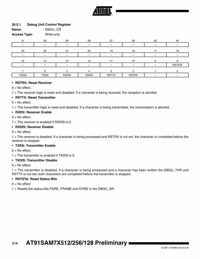
26.5.1 Debug Unit Control Register
Name: DBGU_CR
Access Type: Write-only
• RSTRX: Reset Receiver
0 = No effect.
1 = The receiver logic is reset and disabled. If a character is being received, the reception is aborted.
• RSTTX: Reset Transmitter
0 = No effect.
1 = The transmitter logic is reset and disabled. If a character is being transmitted, the transmission is aborted.
• RXEN: Receiver Enable
0 = No effect.
1 = The receiver is enabled if RXDIS is 0.
• RXDIS: Receiver Disable
0 = No effect.
1 = The receiver is disabled. If a character is being processed and RSTRX is not set, the character is completed before the receiver is stopped.
• TXEN: Transmitter Enable
0 = No effect.
1 = The transmitter is enabled if TXDIS is 0.
• TXDIS: Transmitter Disable
0 = No effect.
1 = The transmitter is disabled. If a character is being processed and a character has been written the DBGU_THR and RSTTX is not set, both characters are completed before the transmitter is stopped.
• RSTSTA: Reset Status Bits
0 = No effect.
1 = Resets the status bits PARE, FRAME and OVRE in the DBGU_SR.
31 30 29 28 27 26 25 24
– – – – – – – –
23 22 21 20 19 18 17 16
– – – – – – – –
15 14 13 12 11 10 9 8
– – – – – – – RSTSTA
7 6 5 4 3 2 1 0
TXDIS TXEN RXDIS RXEN RSTTX RSTRX – –
2146120F–ATARM–03-Oct-06
AT91SAM7X512/256/128 Preliminary

AT91SAM7X512/256/128 Preliminary
26.5.2 Debug Unit Mode Register
Name: DBGU_MR
Access Type: Read/Write
• PAR: Parity Type
• CHMODE: Channel Mode
31 30 29 28 27 26 25 24
– – – – – – – –
23 22 21 20 19 18 17 16
– – – – – – – –
15 14 13 12 11 10 9 8
CHMODE – – PAR –
7 6 5 4 3 2 1 0
– – – – – – – –
PAR Parity Type
0 0 0 Even parity
0 0 1 Odd parity
0 1 0 Space: parity forced to 0
0 1 1 Mark: parity forced to 1
1 x x No parity
CHMODE Mode Description
0 0 Normal Mode
0 1 Automatic Echo
1 0 Local Loopback
1 1 Remote Loopback
2156120F–ATARM–03-Oct-06
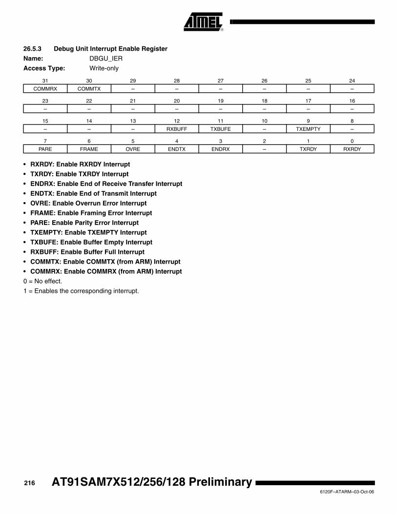
26.5.3 Debug Unit Interrupt Enable Register
Name: DBGU_IER
Access Type: Write-only
• RXRDY: Enable RXRDY Interrupt
• TXRDY: Enable TXRDY Interrupt
• ENDRX: Enable End of Receive Transfer Interrupt
• ENDTX: Enable End of Transmit Interrupt
• OVRE: Enable Overrun Error Interrupt
• FRAME: Enable Framing Error Interrupt
• PARE: Enable Parity Error Interrupt
• TXEMPTY: Enable TXEMPTY Interrupt
• TXBUFE: Enable Buffer Empty Interrupt
• RXBUFF: Enable Buffer Full Interrupt
• COMMTX: Enable COMMTX (from ARM) Interrupt
• COMMRX: Enable COMMRX (from ARM) Interrupt
0 = No effect.
1 = Enables the corresponding interrupt.
31 30 29 28 27 26 25 24
COMMRX COMMTX – – – – – –
23 22 21 20 19 18 17 16
– – – – – – – –
15 14 13 12 11 10 9 8
– – – RXBUFF TXBUFE – TXEMPTY –
7 6 5 4 3 2 1 0
PARE FRAME OVRE ENDTX ENDRX – TXRDY RXRDY
2166120F–ATARM–03-Oct-06
AT91SAM7X512/256/128 Preliminary

AT91SAM7X512/256/128 Preliminary
26.5.4 Debug Unit Interrupt Disable Register
Name: DBGU_IDR
Access Type: Write-only
• RXRDY: Disable RXRDY Interrupt
• TXRDY: Disable TXRDY Interrupt
• ENDRX: Disable End of Receive Transfer Interrupt
• ENDTX: Disable End of Transmit Interrupt
• OVRE: Disable Overrun Error Interrupt
• FRAME: Disable Framing Error Interrupt
• PARE: Disable Parity Error Interrupt
• TXEMPTY: Disable TXEMPTY Interrupt
• TXBUFE: Disable Buffer Empty Interrupt
• RXBUFF: Disable Buffer Full Interrupt
• COMMTX: Disable COMMTX (from ARM) Interrupt
• COMMRX: Disable COMMRX (from ARM) Interrupt
0 = No effect.
1 = Disables the corresponding interrupt.
31 30 29 28 27 26 25 24
COMMRX COMMTX – – – – – –
23 22 21 20 19 18 17 16
– – – – – – – –
15 14 13 12 11 10 9 8
– – – RXBUFF TXBUFE – TXEMPTY –
7 6 5 4 3 2 1 0
PARE FRAME OVRE ENDTX ENDRX – TXRDY RXRDY
2176120F–ATARM–03-Oct-06

26.5.5 Debug Unit Interrupt Mask Register
Name: DBGU_IMR
Access Type: Read-only
• RXRDY: Mask RXRDY Interrupt
• TXRDY: Disable TXRDY Interrupt
• ENDRX: Mask End of Receive Transfer Interrupt
• ENDTX: Mask End of Transmit Interrupt
• OVRE: Mask Overrun Error Interrupt
• FRAME: Mask Framing Error Interrupt
• PARE: Mask Parity Error Interrupt
• TXEMPTY: Mask TXEMPTY Interrupt
• TXBUFE: Mask TXBUFE Interrupt
• RXBUFF: Mask RXBUFF Interrupt
• COMMTX: Mask COMMTX Interrupt
• COMMRX: Mask COMMRX Interrupt
0 = The corresponding interrupt is disabled.
1 = The corresponding interrupt is enabled.
31 30 29 28 27 26 25 24
COMMRX COMMTX – – – – – –
23 22 21 20 19 18 17 16
– – – – – – – –
15 14 13 12 11 10 9 8
– – – RXBUFF TXBUFE – TXEMPTY –
7 6 5 4 3 2 1 0
PARE FRAME OVRE ENDTX ENDRX – TXRDY RXRDY
2186120F–ATARM–03-Oct-06
AT91SAM7X512/256/128 Preliminary
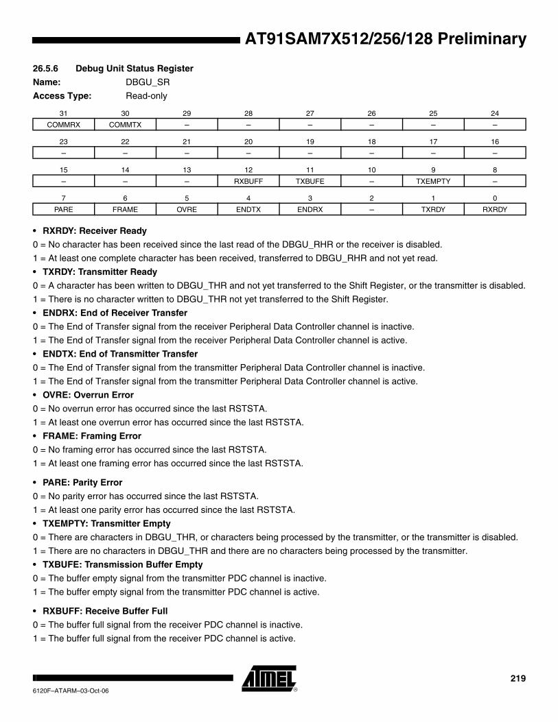
AT91SAM7X512/256/128 Preliminary
26.5.6 Debug Unit Status Register
Name: DBGU_SR
Access Type: Read-only
• RXRDY: Receiver Ready
0 = No character has been received since the last read of the DBGU_RHR or the receiver is disabled.
1 = At least one complete character has been received, transferred to DBGU_RHR and not yet read.
• TXRDY: Transmitter Ready
0 = A character has been written to DBGU_THR and not yet transferred to the Shift Register, or the transmitter is disabled.
1 = There is no character written to DBGU_THR not yet transferred to the Shift Register.
• ENDRX: End of Receiver Transfer
0 = The End of Transfer signal from the receiver Peripheral Data Controller channel is inactive.
1 = The End of Transfer signal from the receiver Peripheral Data Controller channel is active.
• ENDTX: End of Transmitter Transfer
0 = The End of Transfer signal from the transmitter Peripheral Data Controller channel is inactive.
1 = The End of Transfer signal from the transmitter Peripheral Data Controller channel is active.
• OVRE: Overrun Error
0 = No overrun error has occurred since the last RSTSTA.
1 = At least one overrun error has occurred since the last RSTSTA.
• FRAME: Framing Error
0 = No framing error has occurred since the last RSTSTA.
1 = At least one framing error has occurred since the last RSTSTA.
• PARE: Parity Error
0 = No parity error has occurred since the last RSTSTA.
1 = At least one parity error has occurred since the last RSTSTA.
• TXEMPTY: Transmitter Empty
0 = There are characters in DBGU_THR, or characters being processed by the transmitter, or the transmitter is disabled.
1 = There are no characters in DBGU_THR and there are no characters being processed by the transmitter.
• TXBUFE: Transmission Buffer Empty
0 = The buffer empty signal from the transmitter PDC channel is inactive.
1 = The buffer empty signal from the transmitter PDC channel is active.
• RXBUFF: Receive Buffer Full
0 = The buffer full signal from the receiver PDC channel is inactive.
1 = The buffer full signal from the receiver PDC channel is active.
31 30 29 28 27 26 25 24
COMMRX COMMTX – – – – – –
23 22 21 20 19 18 17 16
– – – – – – – –
15 14 13 12 11 10 9 8
– – – RXBUFF TXBUFE – TXEMPTY –
7 6 5 4 3 2 1 0
PARE FRAME OVRE ENDTX ENDRX – TXRDY RXRDY
2196120F–ATARM–03-Oct-06

• COMMTX: Debug Communication Channel Write Status
0 = COMMTX from the ARM processor is inactive.
1 = COMMTX from the ARM processor is active.
• COMMRX: Debug Communication Channel Read Status
0 = COMMRX from the ARM processor is inactive.
1 = COMMRX from the ARM processor is active.
2206120F–ATARM–03-Oct-06
AT91SAM7X512/256/128 Preliminary

AT91SAM7X512/256/128 Preliminary
26.5.7 Debug Unit Receiver Holding Register
Name: DBGU_RHR
Access Type: Read-only
• RXCHR: Received Character
Last received character if RXRDY is set.
26.5.8 Debug Unit Transmit Holding Register
Name: DBGU_THR
Access Type: Write-only
• TXCHR: Character to be Transmitted
Next character to be transmitted after the current character if TXRDY is not set.
31 30 29 28 27 26 25 24
– – – – – – – –
23 22 21 20 19 18 17 16
– – – – – – – –
15 14 13 12 11 10 9 8
– – – – – – – –
7 6 5 4 3 2 1 0
RXCHR
31 30 29 28 27 26 25 24
– – – – – – – –
23 22 21 20 19 18 17 16
– – – – – – – –
15 14 13 12 11 10 9 8
– – – – – – – –
7 6 5 4 3 2 1 0
TXCHR
2216120F–ATARM–03-Oct-06

26.5.9 Debug Unit Baud Rate Generator Register
Name: DBGU_BRGR
Access Type: Read/Write
• CD: Clock Divisor
31 30 29 28 27 26 25 24
– – – – – – – –
23 22 21 20 19 18 17 16
– – – – – – – –
15 14 13 12 11 10 9 8
CD
7 6 5 4 3 2 1 0
CD
CD Baud Rate Clock
0 Disabled
1 MCK
2 to 65535 MCK / (CD x 16)
2226120F–ATARM–03-Oct-06
AT91SAM7X512/256/128 Preliminary

AT91SAM7X512/256/128 Preliminary
26.5.10 Debug Unit Chip ID Register
Name: DBGU_CIDR
Access Type: Read-only
• VERSION: Version of the Device
• EPROC: Embedded Processor
• NVPSIZ: Nonvolatile Program Memory Size
31 30 29 28 27 26 25 24
EXT NVPTYP ARCH
23 22 21 20 19 18 17 16
ARCH SRAMSIZ
15 14 13 12 11 10 9 8
NVPSIZ2 NVPSIZ
7 6 5 4 3 2 1 0
EPROC VERSION
EPROC Processor
0 0 1 ARM946ES™
0 1 0 ARM7TDMI®
1 0 0 ARM920T™
1 0 1 ARM926EJS™
NVPSIZ Size
0 0 0 0 None
0 0 0 1 8K bytes
0 0 1 0 16K bytes
0 0 1 1 32K bytes
0 1 0 0 Reserved
0 1 0 1 64K bytes
0 1 1 0 Reserved
0 1 1 1 128K bytes
1 0 0 0 Reserved
1 0 0 1 256K bytes
1 0 1 0 512K bytes
1 0 1 1 Reserved
1 1 0 0 1024K bytes
1 1 0 1 Reserved
1 1 1 0 2048K bytes
1 1 1 1 Reserved
2236120F–ATARM–03-Oct-06

• NVPSIZ2 Second Nonvolatile Program Memory Size
• SRAMSIZ: Internal SRAM Size
NVPSIZ2 Size
0 0 0 0 None
0 0 0 1 8K bytes
0 0 1 0 16K bytes
0 0 1 1 32K bytes
0 1 0 0 Reserved
0 1 0 1 64K bytes
0 1 1 0 Reserved
0 1 1 1 128K bytes
1 0 0 0 Reserved
1 0 0 1 256K bytes
1 0 1 0 512K bytes
1 0 1 1 Reserved
1 1 0 0 1024K bytes
1 1 0 1 Reserved
1 1 1 0 2048K bytes
1 1 1 1 Reserved
SRAMSIZ Size
0 0 0 0 Reserved
0 0 0 1 1K bytes
0 0 1 0 2K bytes
0 0 1 1 Reserved
0 1 0 0 112K bytes
0 1 0 1 4K bytes
0 1 1 0 80K bytes
0 1 1 1 160K bytes
1 0 0 0 8K bytes
1 0 0 1 16K bytes
1 0 1 0 32K bytes
1 0 1 1 64K bytes
1 1 0 0 128K bytes
1 1 0 1 256K bytes
1 1 1 0 96K bytes
1 1 1 1 512K bytes
2246120F–ATARM–03-Oct-06
AT91SAM7X512/256/128 Preliminary

AT91SAM7X512/256/128 Preliminary
• ARCH: Architecture Identifier
• NVPTYP: Nonvolatile Program Memory Type
• EXT: Extension Flag
0 = Chip ID has a single register definition without extension
1 = An extended Chip ID exists.
ARCH
ArchitectureHex Bin
0x19 0001 1001 AT91SAM9xx Series
0x29 0010 1001 AT91SAM9XExx Series
0x34 0011 0100 AT91x34 Series
0x39 0011 1001 CAP9 Series
0x40 0100 0000 AT91x40 Series
0x42 0100 0010 AT91x42 Series
0x55 0101 0101 AT91x55 Series
0x60 0101 0000 AT91SAM7Axx Series
0x63 0110 0011 AT91x63 Series
0x70 0111 0000 AT91SAM7Sxx Series
0x71 0111 0001 AT91SAM7XCxx Series
0x72 0111 0010 AT91SAM7SExx Series
0x73 0111 0011 AT91SAM7Lxx Series
0x75 0111 0101 AT91SAM7Xxx Series
0x92 1001 0010 AT91x92 Series
0xF0 1111 0001 AT75Cxx Series
NVPTYP Memory
0 0 0 ROM
0 0 1 ROMless or on-chip Flash
1 0 0 SRAM emulating ROM
0 1 0 Embedded Flash Memory
0 1 1ROM and Embedded Flash Memory
NVPSIZ is ROM size NVPSIZ2 is Flash size
2256120F–ATARM–03-Oct-06

26.5.11 Debug Unit Chip ID Extension Register
Name: DBGU_EXID
Access Type: Read-only
• EXID: Chip ID Extension
Reads 0 if the bit EXT in DBGU_CIDR is 0.
26.5.12 Debug Unit Force NTRST RegisterName: DBGU_FNR
Access Type: Read/Write
• FNTRST: Force NTRST
0 = NTRST of the ARM processor’s TAP controller is driven by the power_on_reset signal.
1 = NTRST of the ARM processor’s TAP controller is held low.
31 30 29 28 27 26 25 24
EXID
23 22 21 20 19 18 17 16
EXID
15 14 13 12 11 10 9 8
EXID
7 6 5 4 3 2 1 0
EXID
31 30 29 28 27 26 25 24
– – – – – – – –
23 22 21 20 19 18 17 16
– – – – – – – –
15 14 13 12 11 10 9 8
– – – – – – – –
7 6 5 4 3 2 1 0
– – – – – – – FNTRST
2266120F–ATARM–03-Oct-06
AT91SAM7X512/256/128 Preliminary
AT91SAM7X512/256/128 Preliminary
27. Parallel Input/Output Controller (PIO)
27.1 Overview
The Parallel Input/Output Controller (PIO) manages up to 32 fully programmable input/output lines. Each I/O line may be dedicated as a general-purpose I/O or be assigned to a function of an embedded peripheral. This assures effective optimization of the pins of a product.
Each I/O line is associated with a bit number in all of the 32-bit registers of the 32-bit wide User Interface.
Each I/O line of the PIO Controller features:
• An input change interrupt enabling level change detection on any I/O line.
• A glitch filter providing rejection of pulses lower than one-half of clock cycle.
• Multi-drive capability similar to an open drain I/O line.
• Control of the pull-up of the I/O line.
• Input visibility and output control.
The PIO Controller also features a synchronous output providing up to 32 bits of data output in a single write operation.
2276120F–ATARM–03-Oct-06

27.2 Block Diagram
Figure 27-1. Block Diagram
27.3 Application Block Diagram
Figure 27-2. Application Block Diagram
Embedded Peripheral
Embedded Peripheral
PIO Interrupt
PIO Controller
Up to 32 pins
PMC
Up to 32 peripheral IOs
Up to 32 peripheral IOs
PIO Clock
APB
AIC
Data, Enable
PIN 31
PIN 1
PIN 0
Data, Enable
On-Chip Peripherals
PIO Controller
On-Chip Peripheral DriversControl & Command
DriverKeyboard Driver
Keyboard Driver General Purpose I/Os External Devices
2286120F–ATARM–03-Oct-06
AT91SAM7X512/256/128 Preliminary
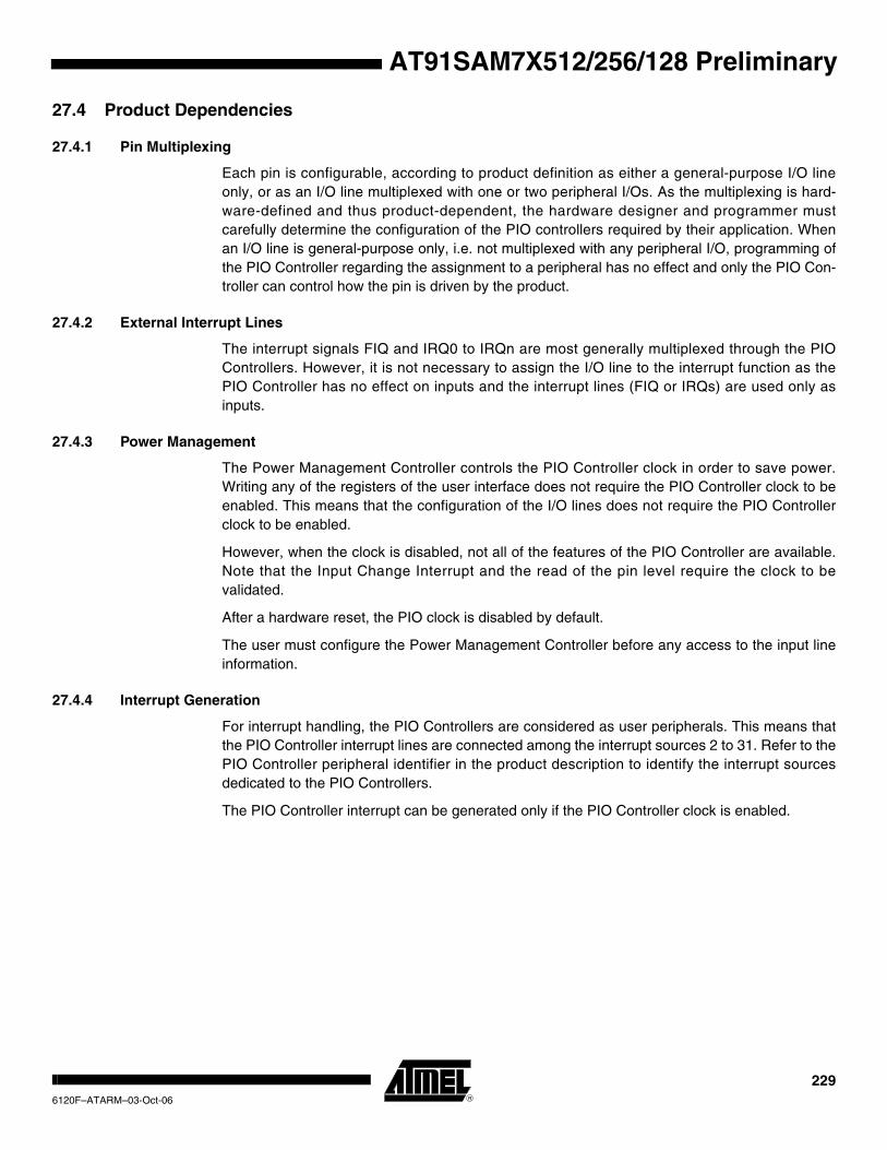
AT91SAM7X512/256/128 Preliminary
27.4 Product Dependencies
27.4.1 Pin Multiplexing
Each pin is configurable, according to product definition as either a general-purpose I/O line only, or as an I/O line multiplexed with one or two peripheral I/Os. As the multiplexing is hard-ware-defined and thus product-dependent, the hardware designer and programmer must carefully determine the configuration of the PIO controllers required by their application. When an I/O line is general-purpose only, i.e. not multiplexed with any peripheral I/O, programming of the PIO Controller regarding the assignment to a peripheral has no effect and only the PIO Con-troller can control how the pin is driven by the product.
27.4.2 External Interrupt Lines
The interrupt signals FIQ and IRQ0 to IRQn are most generally multiplexed through the PIO Controllers. However, it is not necessary to assign the I/O line to the interrupt function as the PIO Controller has no effect on inputs and the interrupt lines (FIQ or IRQs) are used only as inputs.
27.4.3 Power Management
The Power Management Controller controls the PIO Controller clock in order to save power. Writing any of the registers of the user interface does not require the PIO Controller clock to be enabled. This means that the configuration of the I/O lines does not require the PIO Controller clock to be enabled.
However, when the clock is disabled, not all of the features of the PIO Controller are available. Note that the Input Change Interrupt and the read of the pin level require the clock to be validated.
After a hardware reset, the PIO clock is disabled by default.
The user must configure the Power Management Controller before any access to the input line information.
27.4.4 Interrupt Generation
For interrupt handling, the PIO Controllers are considered as user peripherals. This means that the PIO Controller interrupt lines are connected among the interrupt sources 2 to 31. Refer to the PIO Controller peripheral identifier in the product description to identify the interrupt sources dedicated to the PIO Controllers.
The PIO Controller interrupt can be generated only if the PIO Controller clock is enabled.
2296120F–ATARM–03-Oct-06

27.5 Functional Description
The PIO Controller features up to 32 fully-programmable I/O lines. Most of the control logic asso-ciated to each I/O is represented in Figure 27-3. In this description each signal shown represents but one of up to 32 possible indexes.
Figure 27-3. I/O Line Control Logic
1
0
1
0
1
0
GlitchFilter
Peripheral B Input
Peripheral A Input
1
0
PIO_IFDR[0]
PIO_IFSR[0]
PIO_IFER[0]
EdgeDetector
PIO_PDSR[0] PIO_ISR[0]
PIO_IDR[0]
PIO_IMR[0]
PIO_IER[0]
PIO Interrupt
(Up to 32 possible inputs)
PIO_ISR[31]
PIO_IDR[31]
PIO_IMR[31]
PIO_IER[31]
Pad
1
0
PIO_PUDR[0]
PIO_PUSR[0]
PIO_PUER[0]
PIO_MDDR[0]
PIO_MDSR[0]
PIO_MDER[0]
PIO_CODR[0]
PIO_ODSR[0]
PIO_SODR[0]
PIO_PDR[0]
PIO_PSR[0]
PIO_PER[0]
1
0
1
0
PIO_BSR[0]
PIO_ABSR[0]
PIO_ASR[0]
Peripheral BOutput Enable
Peripheral AOutput Enable
Peripheral BOutput
Peripheral AOutput
PIO_ODR[0]
PIO_OSR[0]
PIO_OER[0]
2306120F–ATARM–03-Oct-06
AT91SAM7X512/256/128 Preliminary

AT91SAM7X512/256/128 Preliminary
27.5.1 Pull-up Resistor Control
Each I/O line is designed with an embedded pull-up resistor. The pull-up resistor can be enabled or disabled by writing respectively PIO_PUER (Pull-up Enable Register) and PIO_PUDR (Pull-up Disable Resistor). Writing in these registers results in setting or clearing the corresponding bit in PIO_PUSR (Pull-up Status Register). Reading a 1 in PIO_PUSR means the pull-up is dis-abled and reading a 0 means the pull-up is enabled.
Control of the pull-up resistor is possible regardless of the configuration of the I/O line.
After reset, all of the pull-ups are enabled, i.e. PIO_PUSR resets at the value 0x0.
27.5.2 I/O Line or Peripheral Function Selection
When a pin is multiplexed with one or two peripheral functions, the selection is controlled with the registers PIO_PER (PIO Enable Register) and PIO_PDR (PIO Disable Register). The regis-ter PIO_PSR (PIO Status Register) is the result of the set and clear registers and indicates whether the pin is controlled by the corresponding peripheral or by the PIO Controller. A value of 0 indicates that the pin is controlled by the corresponding on-chip peripheral selected in the PIO_ABSR (AB Select Status Register). A value of 1 indicates the pin is controlled by the PIO controller.
If a pin is used as a general purpose I/O line (not multiplexed with an on-chip peripheral), PIO_PER and PIO_PDR have no effect and PIO_PSR returns 1 for the corresponding bit.
After reset, most generally, the I/O lines are controlled by the PIO controller, i.e. PIO_PSR resets at 1. However, in some events, it is important that PIO lines are controlled by the periph-eral (as in the case of memory chip select lines that must be driven inactive after reset or for address lines that must be driven low for booting out of an external memory). Thus, the reset value of PIO_PSR is defined at the product level, depending on the multiplexing of the device.
27.5.3 Peripheral A or B Selection
The PIO Controller provides multiplexing of up to two peripheral functions on a single pin. The selection is performed by writing PIO_ASR (A Select Register) and PIO_BSR (Select B Regis-ter). PIO_ABSR (AB Select Status Register) indicates which peripheral line is currently selected. For each pin, the corresponding bit at level 0 means peripheral A is selected whereas the corre-sponding bit at level 1 indicates that peripheral B is selected.
Note that multiplexing of peripheral lines A and B only affects the output line. The peripheral input lines are always connected to the pin input.
After reset, PIO_ABSR is 0, thus indicating that all the PIO lines are configured on peripheral A. However, peripheral A generally does not drive the pin as the PIO Controller resets in I/O line mode.
Writing in PIO_ASR and PIO_BSR manages PIO_ABSR regardless of the configuration of the pin. However, assignment of a pin to a peripheral function requires a write in the corresponding peripheral selection register (PIO_ASR or PIO_BSR) in addition to a write in PIO_PDR.
27.5.4 Output Control
When the I/0 line is assigned to a peripheral function, i.e. the corresponding bit in PIO_PSR is at 0, the drive of the I/O line is controlled by the peripheral. Peripheral A or B, depending on the value in PIO_ABSR, determines whether the pin is driven or not.
2316120F–ATARM–03-Oct-06

When the I/O line is controlled by the PIO controller, the pin can be configured to be driven. This is done by writing PIO_OER (Output Enable Register) and PIO_ODR (Output Disable Register). The results of these write operations are detected in PIO_OSR (Output Status Register). When a bit in this register is at 0, the corresponding I/O line is used as an input only. When the bit is at 1, the corresponding I/O line is driven by the PIO controller.
The level driven on an I/O line can be determined by writing in PIO_SODR (Set Output Data Register) and PIO_CODR (Clear Output Data Register). These write operations respectively set and clear PIO_ODSR (Output Data Status Register), which represents the data driven on the I/O lines. Writing in PIO_OER and PIO_ODR manages PIO_OSR whether the pin is configured to be controlled by the PIO controller or assigned to a peripheral function. This enables configura-tion of the I/O line prior to setting it to be managed by the PIO Controller.
Similarly, writing in PIO_SODR and PIO_CODR effects PIO_ODSR. This is important as it defines the first level driven on the I/O line.
27.5.5 Synchronous Data Output
Controlling all parallel busses using several PIOs requires two successive write operations in the PIO_SODR and PIO_CODR registers. This may lead to unexpected transient values. The PIO controller offers a direct control of PIO outputs by single write access to PIO_ODSR (Output Data Status Register). Only bits unmasked by PIO_OSWSR (Output Write Status Register) are written. The mask bits in the PIO_OWSR are set by writing to PIO_OWER (Output Write Enable Register) and cleared by writing to PIO_OWDR (Output Write Disable Register).
After reset, the synchronous data output is disabled on all the I/O lines as PIO_OWSR resets at 0x0.
27.5.6 Multi Drive Control (Open Drain)
Each I/O can be independently programmed in Open Drain by using the Multi Drive feature. This feature permits several drivers to be connected on the I/O line which is driven low only by each device. An external pull-up resistor (or enabling of the internal one) is generally required to guar-antee a high level on the line.
The Multi Drive feature is controlled by PIO_MDER (Multi-driver Enable Register) and PIO_MDDR (Multi-driver Disable Register). The Multi Drive can be selected whether the I/O line is controlled by the PIO controller or assigned to a peripheral function. PIO_MDSR (Multi-driver Status Register) indicates the pins that are configured to support external drivers.
After reset, the Multi Drive feature is disabled on all pins, i.e. PIO_MDSR resets at value 0x0.
27.5.7 Output Line Timings
Figure 27-4 shows how the outputs are driven either by writing PIO_SODR or PIO_CODR, or by directly writing PIO_ODSR. This last case is valid only if the corresponding bit in PIO_OWSR is set. Figure 27-4 also shows when the feedback in PIO_PDSR is available.
2326120F–ATARM–03-Oct-06
AT91SAM7X512/256/128 Preliminary
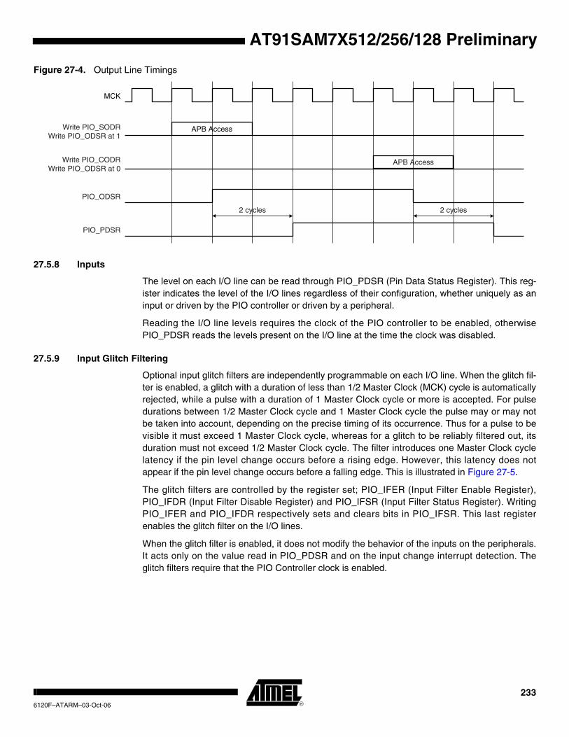
AT91SAM7X512/256/128 Preliminary
Figure 27-4. Output Line Timings
27.5.8 Inputs
The level on each I/O line can be read through PIO_PDSR (Pin Data Status Register). This reg-ister indicates the level of the I/O lines regardless of their configuration, whether uniquely as an input or driven by the PIO controller or driven by a peripheral.
Reading the I/O line levels requires the clock of the PIO controller to be enabled, otherwise PIO_PDSR reads the levels present on the I/O line at the time the clock was disabled.
27.5.9 Input Glitch Filtering
Optional input glitch filters are independently programmable on each I/O line. When the glitch fil-ter is enabled, a glitch with a duration of less than 1/2 Master Clock (MCK) cycle is automatically rejected, while a pulse with a duration of 1 Master Clock cycle or more is accepted. For pulse durations between 1/2 Master Clock cycle and 1 Master Clock cycle the pulse may or may not be taken into account, depending on the precise timing of its occurrence. Thus for a pulse to be visible it must exceed 1 Master Clock cycle, whereas for a glitch to be reliably filtered out, its duration must not exceed 1/2 Master Clock cycle. The filter introduces one Master Clock cycle latency if the pin level change occurs before a rising edge. However, this latency does not appear if the pin level change occurs before a falling edge. This is illustrated in Figure 27-5.
The glitch filters are controlled by the register set; PIO_IFER (Input Filter Enable Register), PIO_IFDR (Input Filter Disable Register) and PIO_IFSR (Input Filter Status Register). Writing PIO_IFER and PIO_IFDR respectively sets and clears bits in PIO_IFSR. This last register enables the glitch filter on the I/O lines.
When the glitch filter is enabled, it does not modify the behavior of the inputs on the peripherals. It acts only on the value read in PIO_PDSR and on the input change interrupt detection. The glitch filters require that the PIO Controller clock is enabled.
2 cycles
APB Access
2 cycles
APB Access
MCK
Write PIO_SODRWrite PIO_ODSR at 1
PIO_ODSR
PIO_PDSR
Write PIO_CODRWrite PIO_ODSR at 0
2336120F–ATARM–03-Oct-06
Figure 27-5. Input Glitch Filter Timing
27.5.10 Input Change Interrupt
The PIO Controller can be programmed to generate an interrupt when it detects an input change on an I/O line. The Input Change Interrupt is controlled by writing PIO_IER (Interrupt Enable Register) and PIO_IDR (Interrupt Disable Register), which respectively enable and disable the input change interrupt by setting and clearing the corresponding bit in PIO_IMR (Interrupt Mask Register). As Input change detection is possible only by comparing two successive samplings of the input of the I/O line, the PIO Controller clock must be enabled. The Input Change Interrupt is available, regardless of the configuration of the I/O line, i.e. configured as an input only, con-trolled by the PIO Controller or assigned to a peripheral function.
When an input change is detected on an I/O line, the corresponding bit in PIO_ISR (Interrupt Status Register) is set. If the corresponding bit in PIO_IMR is set, the PIO Controller interrupt line is asserted. The interrupt signals of the thirty-two channels are ORed-wired together to gen-erate a single interrupt signal to the Advanced Interrupt Controller.
When the software reads PIO_ISR, all the interrupts are automatically cleared. This signifies that all the interrupts that are pending when PIO_ISR is read must be handled.
Figure 27-6. Input Change Interrupt Timings
MCK
Pin Level
PIO_PDSRif PIO_IFSR = 0
PIO_PDSRif PIO_IFSR = 1
1 cycle 1 cycle 1 cycle
up to 1.5 cycles
2 cycles
up to 2.5 cycles up to 2 cycles
1 cycle
1 cycle
MCK
Pin Level
Read PIO_ISR APB Access
PIO_ISR
APB Access
2346120F–ATARM–03-Oct-06
AT91SAM7X512/256/128 Preliminary

AT91SAM7X512/256/128 Preliminary
27.6 I/O Lines Programming Example
The programing example as shown in Table 27-1 below is used to define the following configuration.
• 4-bit output port on I/O lines 0 to 3, (should be written in a single write operation), open-drain, with pull-up resistor
• Four output signals on I/O lines 4 to 7 (to drive LEDs for example), driven high and low, no pull-up resistor
• Four input signals on I/O lines 8 to 11 (to read push-button states for example), with pull-up resistors, glitch filters and input change interrupts
• Four input signals on I/O line 12 to 15 to read an external device status (polled, thus no input change interrupt), no pull-up resistor, no glitch filter
• I/O lines 16 to 19 assigned to peripheral A functions with pull-up resistor
• I/O lines 20 to 23 assigned to peripheral B functions, no pull-up resistor
• I/O line 24 to 27 assigned to peripheral A with Input Change Interrupt and pull-up resistor
Table 27-1. Programming Example
Register Value to be Written
PIO_PER 0x0000 FFFF
PIO_PDR 0x0FFF 0000
PIO_OER 0x0000 00FF
PIO_ODR 0x0FFF FF00
PIO_IFER 0x0000 0F00
PIO_IFDR 0x0FFF F0FF
PIO_SODR 0x0000 0000
PIO_CODR 0x0FFF FFFF
PIO_IER 0x0F00 0F00
PIO_IDR 0x00FF F0FF
PIO_MDER 0x0000 000F
PIO_MDDR 0x0FFF FFF0
PIO_PUDR 0x00F0 00F0
PIO_PUER 0x0F0F FF0F
PIO_ASR 0x0F0F 0000
PIO_BSR 0x00F0 0000
PIO_OWER 0x0000 000F
PIO_OWDR 0x0FFF FFF0
2356120F–ATARM–03-Oct-06

27.7 Parallel Input/Output Controller (PIO) User Interface
Each I/O line controlled by the PIO Controller is associated with a bit in each of the PIO Control-ler User Interface registers. Each register is 32 bits wide. If a parallel I/O line is not defined, writing to the corresponding bits has no effect. Undefined bits read zero. If the I/O line is not mul-tiplexed with any peripheral, the I/O line is controlled by the PIO Controller and PIO_PSR returns 1 systematically.
Table 27-2. Parallel Input/Output Controller (PIO) Register Mapping
Offset Register Name Access Reset Value
0x0000 PIO Enable Register PIO_PER Write-only –
0x0004 PIO Disable Register PIO_PDR Write-only –
0x0008 PIO Status Register (1) PIO_PSR Read-only 0x0000 0000
0x000C Reserved
0x0010 Output Enable Register PIO_OER Write-only –
0x0014 Output Disable Register PIO_ODR Write-only –
0x0018 Output Status Register PIO_OSR Read-only 0x0000 0000
0x001C Reserved
0x0020 Glitch Input Filter Enable Register PIO_IFER Write-only –
0x0024 Glitch Input Filter Disable Register PIO_IFDR Write-only –
0x0028 Glitch Input Filter Status Register PIO_IFSR Read-only 0x0000 0000
0x002C Reserved
0x0030 Set Output Data Register PIO_SODR Write-only –
0x0034 Clear Output Data Register PIO_CODR Write-only –
0x0038 Output Data Status Register(2) PIO_ODSR Read-only 0x0000 0000
0x003C Pin Data Status Register(3) PIO_PDSR Read-only
0x0040 Interrupt Enable Register PIO_IER Write-only –
0x0044 Interrupt Disable Register PIO_IDR Write-only –
0x0048 Interrupt Mask Register PIO_IMR Read-only 0x00000000
0x004C Interrupt Status Register(4) PIO_ISR Read-only 0x00000000
0x0050 Multi-driver Enable Register PIO_MDER Write-only –
0x0054 Multi-driver Disable Register PIO_MDDR Write-only –
0x0058 Multi-driver Status Register PIO_MDSR Read-only 0x00000000
0x005C Reserved
0x0060 Pull-up Disable Register PIO_PUDR Write-only –
0x0064 Pull-up Enable Register PIO_PUER Write-only –
0x0068 Pad Pull-up Status Register PIO_PUSR Read-only 0x00000000
0x006C Reserved
2366120F–ATARM–03-Oct-06
AT91SAM7X512/256/128 Preliminary
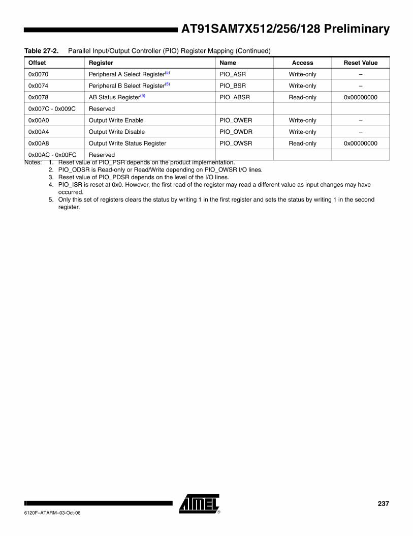
AT91SAM7X512/256/128 Preliminary
Notes: 1. Reset value of PIO_PSR depends on the product implementation.2. PIO_ODSR is Read-only or Read/Write depending on PIO_OWSR I/O lines.3. Reset value of PIO_PDSR depends on the level of the I/O lines. 4. PIO_ISR is reset at 0x0. However, the first read of the register may read a different value as input changes may have
occurred.5. Only this set of registers clears the status by writing 1 in the first register and sets the status by writing 1 in the second
register.
0x0070 Peripheral A Select Register(5) PIO_ASR Write-only –
0x0074 Peripheral B Select Register(5) PIO_BSR Write-only –
0x0078 AB Status Register(5) PIO_ABSR Read-only 0x00000000
0x007C - 0x009C Reserved
0x00A0 Output Write Enable PIO_OWER Write-only –
0x00A4 Output Write Disable PIO_OWDR Write-only –
0x00A8 Output Write Status Register PIO_OWSR Read-only 0x00000000
0x00AC - 0x00FC Reserved
Table 27-2. Parallel Input/Output Controller (PIO) Register Mapping (Continued)
Offset Register Name Access Reset Value
2376120F–ATARM–03-Oct-06

27.7.1 PIO Controller PIO Enable Register
Name: PIO_PER
Access Type: Write-only
• P0-P31: PIO Enable
0 = No effect.
1 = Enables the PIO to control the corresponding pin (disables peripheral control of the pin).
27.7.2 PIO Controller PIO Disable Register
Name: PIO_PDR
Access Type: Write-only
• P0-P31: PIO Disable
0 = No effect.
1 = Disables the PIO from controlling the corresponding pin (enables peripheral control of the pin).
31 30 29 28 27 26 25 24
P31 P30 P29 P28 P27 P26 P25 P24
23 22 21 20 19 18 17 16
P23 P22 P21 P20 P19 P18 P17 P16
15 14 13 12 11 10 9 8
P15 P14 P13 P12 P11 P10 P9 P8
7 6 5 4 3 2 1 0
P7 P6 P5 P4 P3 P2 P1 P0
31 30 29 28 27 26 25 24
P31 P30 P29 P28 P27 P26 P25 P24
23 22 21 20 19 18 17 16
P23 P22 P21 P20 P19 P18 P17 P16
15 14 13 12 11 10 9 8
P15 P14 P13 P12 P11 P10 P9 P8
7 6 5 4 3 2 1 0
P7 P6 P5 P4 P3 P2 P1 P0
2386120F–ATARM–03-Oct-06
AT91SAM7X512/256/128 Preliminary

AT91SAM7X512/256/128 Preliminary
27.7.3 PIO Controller PIO Status Register
Name: PIO_PSR
Access Type: Read-only
• P0-P31: PIO Status
0 = PIO is inactive on the corresponding I/O line (peripheral is active).
1 = PIO is active on the corresponding I/O line (peripheral is inactive).
27.7.4 PIO Controller Output Enable Register
Name: PIO_OER
Access Type: Write-only
• P0-P31: Output Enable
0 = No effect.
1 = Enables the output on the I/O line.
31 30 29 28 27 26 25 24
P31 P30 P29 P28 P27 P26 P25 P24
23 22 21 20 19 18 17 16
P23 P22 P21 P20 P19 P18 P17 P16
15 14 13 12 11 10 9 8
P15 P14 P13 P12 P11 P10 P9 P8
7 6 5 4 3 2 1 0
P7 P6 P5 P4 P3 P2 P1 P0
31 30 29 28 27 26 25 24
P31 P30 P29 P28 P27 P26 P25 P24
23 22 21 20 19 18 17 16
P23 P22 P21 P20 P19 P18 P17 P16
15 14 13 12 11 10 9 8
P15 P14 P13 P12 P11 P10 P9 P8
7 6 5 4 3 2 1 0
P7 P6 P5 P4 P3 P2 P1 P0
2396120F–ATARM–03-Oct-06
27.7.5 PIO Controller Output Disable Register
Name: PIO_ODR
Access Type: Write-only
• P0-P31: Output Disable
0 = No effect.
1 = Disables the output on the I/O line.
27.7.6 PIO Controller Output Status Register
Name: PIO_OSR
Access Type: Read-only
• P0-P31: Output Status
0 = The I/O line is a pure input.
1 = The I/O line is enabled in output.
31 30 29 28 27 26 25 24
P31 P30 P29 P28 P27 P26 P25 P24
23 22 21 20 19 18 17 16
P23 P22 P21 P20 P19 P18 P17 P16
15 14 13 12 11 10 9 8
P15 P14 P13 P12 P11 P10 P9 P8
7 6 5 4 3 2 1 0
P7 P6 P5 P4 P3 P2 P1 P0
31 30 29 28 27 26 25 24
P31 P30 P29 P28 P27 P26 P25 P24
23 22 21 20 19 18 17 16
P23 P22 P21 P20 P19 P18 P17 P16
15 14 13 12 11 10 9 8
P15 P14 P13 P12 P11 P10 P9 P8
7 6 5 4 3 2 1 0
P7 P6 P5 P4 P3 P2 P1 P0
2406120F–ATARM–03-Oct-06
AT91SAM7X512/256/128 Preliminary

AT91SAM7X512/256/128 Preliminary
27.7.7 PIO Controller Input Filter Enable Register
Name: PIO_IFER
Access Type: Write-only
• P0-P31: Input Filter Enable
0 = No effect.
1 = Enables the input glitch filter on the I/O line.
27.7.8 PIO Controller Input Filter Disable Register
Name: PIO_IFDR
Access Type: Write-only
• P0-P31: Input Filter Disable
0 = No effect.
1 = Disables the input glitch filter on the I/O line.
31 30 29 28 27 26 25 24
P31 P30 P29 P28 P27 P26 P25 P24
23 22 21 20 19 18 17 16
P23 P22 P21 P20 P19 P18 P17 P16
15 14 13 12 11 10 9 8
P15 P14 P13 P12 P11 P10 P9 P8
7 6 5 4 3 2 1 0
P7 P6 P5 P4 P3 P2 P1 P0
31 30 29 28 27 26 25 24
P31 P30 P29 P28 P27 P26 P25 P24
23 22 21 20 19 18 17 16
P23 P22 P21 P20 P19 P18 P17 P16
15 14 13 12 11 10 9 8
P15 P14 P13 P12 P11 P10 P9 P8
7 6 5 4 3 2 1 0
P7 P6 P5 P4 P3 P2 P1 P0
2416120F–ATARM–03-Oct-06

27.7.9 PIO Controller Input Filter Status Register
Name: PIO_IFSR
Access Type: Read-only
• P0-P31: Input Filer Status
0 = The input glitch filter is disabled on the I/O line.
1 = The input glitch filter is enabled on the I/O line.
27.7.10 PIO Controller Set Output Data Register
Name: PIO_SODR
Access Type: Write-only
• P0-P31: Set Output Data
0 = No effect.
1 = Sets the data to be driven on the I/O line.
31 30 29 28 27 26 25 24
P31 P30 P29 P28 P27 P26 P25 P24
23 22 21 20 19 18 17 16
P23 P22 P21 P20 P19 P18 P17 P16
15 14 13 12 11 10 9 8
P15 P14 P13 P12 P11 P10 P9 P8
7 6 5 4 3 2 1 0
P7 P6 P5 P4 P3 P2 P1 P0
31 30 29 28 27 26 25 24
P31 P30 P29 P28 P27 P26 P25 P24
23 22 21 20 19 18 17 16
P23 P22 P21 P20 P19 P18 P17 P16
15 14 13 12 11 10 9 8
P15 P14 P13 P12 P11 P10 P9 P8
7 6 5 4 3 2 1 0
P7 P6 P5 P4 P3 P2 P1 P0
2426120F–ATARM–03-Oct-06
AT91SAM7X512/256/128 Preliminary
AT91SAM7X512/256/128 Preliminary
27.7.11 PIO Controller Clear Output Data Register
Name: PIO_CODR
Access Type: Write-only
• P0-P31: Set Output Data
0 = No effect.
1 = Clears the data to be driven on the I/O line.
27.7.12 PIO Controller Output Data Status Register
Name: PIO_ODSR
Access Type: Read-only or Read/Write
• P0-P31: Output Data Status
0 = The data to be driven on the I/O line is 0.
1 = The data to be driven on the I/O line is 1.
31 30 29 28 27 26 25 24
P31 P30 P29 P28 P27 P26 P25 P24
23 22 21 20 19 18 17 16
P23 P22 P21 P20 P19 P18 P17 P16
15 14 13 12 11 10 9 8
P15 P14 P13 P12 P11 P10 P9 P8
7 6 5 4 3 2 1 0
P7 P6 P5 P4 P3 P2 P1 P0
31 30 29 28 27 26 25 24
P31 P30 P29 P28 P27 P26 P25 P24
23 22 21 20 19 18 17 16
P23 P22 P21 P20 P19 P18 P17 P16
15 14 13 12 11 10 9 8
P15 P14 P13 P12 P11 P10 P9 P8
7 6 5 4 3 2 1 0
P7 P6 P5 P4 P3 P2 P1 P0
2436120F–ATARM–03-Oct-06
27.7.13 PIO Controller Pin Data Status Register
Name: PIO_PDSR
Access Type: Read-only
• P0-P31: Output Data Status
0 = The I/O line is at level 0.
1 = The I/O line is at level 1.
27.7.14 PIO Controller Interrupt Enable Register
Name: PIO_IER
Access Type: Write-only
• P0-P31: Input Change Interrupt Enable
0 = No effect.
1 = Enables the Input Change Interrupt on the I/O line.
31 30 29 28 27 26 25 24
P31 P30 P29 P28 P27 P26 P25 P24
23 22 21 20 19 18 17 16
P23 P22 P21 P20 P19 P18 P17 P16
15 14 13 12 11 10 9 8
P15 P14 P13 P12 P11 P10 P9 P8
7 6 5 4 3 2 1 0
P7 P6 P5 P4 P3 P2 P1 P0
31 30 29 28 27 26 25 24
P31 P30 P29 P28 P27 P26 P25 P24
23 22 21 20 19 18 17 16
P23 P22 P21 P20 P19 P18 P17 P16
15 14 13 12 11 10 9 8
P15 P14 P13 P12 P11 P10 P9 P8
7 6 5 4 3 2 1 0
P7 P6 P5 P4 P3 P2 P1 P0
2446120F–ATARM–03-Oct-06
AT91SAM7X512/256/128 Preliminary
AT91SAM7X512/256/128 Preliminary
27.7.15 PIO Controller Interrupt Disable Register
Name: PIO_IDR
Access Type: Write-only
• P0-P31: Input Change Interrupt Disable
0 = No effect.
1 = Disables the Input Change Interrupt on the I/O line.
27.7.16 PIO Controller Interrupt Mask Register
Name: PIO_IMR
Access Type: Read-only
• P0-P31: Input Change Interrupt Mask
0 = Input Change Interrupt is disabled on the I/O line.
1 = Input Change Interrupt is enabled on the I/O line.
31 30 29 28 27 26 25 24
P31 P30 P29 P28 P27 P26 P25 P24
23 22 21 20 19 18 17 16
P23 P22 P21 P20 P19 P18 P17 P16
15 14 13 12 11 10 9 8
P15 P14 P13 P12 P11 P10 P9 P8
7 6 5 4 3 2 1 0
P7 P6 P5 P4 P3 P2 P1 P0
31 30 29 28 27 26 25 24
P31 P30 P29 P28 P27 P26 P25 P24
23 22 21 20 19 18 17 16
P23 P22 P21 P20 P19 P18 P17 P16
15 14 13 12 11 10 9 8
P15 P14 P13 P12 P11 P10 P9 P8
7 6 5 4 3 2 1 0
P7 P6 P5 P4 P3 P2 P1 P0
2456120F–ATARM–03-Oct-06

27.7.17 PIO Controller Interrupt Status Register
Name: PIO_ISR
Access Type: Read-only
• P0-P31: Input Change Interrupt Status
0 = No Input Change has been detected on the I/O line since PIO_ISR was last read or since reset.
1 = At least one Input Change has been detected on the I/O line since PIO_ISR was last read or since reset.
27.7.18 PIO Multi-driver Enable Register
Name: PIO_MDER
Access Type: Write-only
• P0-P31: Multi Drive Enable.
0 = No effect.
1 = Enables Multi Drive on the I/O line.
31 30 29 28 27 26 25 24
P31 P30 P29 P28 P27 P26 P25 P24
23 22 21 20 19 18 17 16
P23 P22 P21 P20 P19 P18 P17 P16
15 14 13 12 11 10 9 8
P15 P14 P13 P12 P11 P10 P9 P8
7 6 5 4 3 2 1 0
P7 P6 P5 P4 P3 P2 P1 P0
31 30 29 28 27 26 25 24
P31 P30 P29 P28 P27 P26 P25 P24
23 22 21 20 19 18 17 16
P23 P22 P21 P20 P19 P18 P17 P16
15 14 13 12 11 10 9 8
P15 P14 P13 P12 P11 P10 P9 P8
7 6 5 4 3 2 1 0
P7 P6 P5 P4 P3 P2 P1 P0
2466120F–ATARM–03-Oct-06
AT91SAM7X512/256/128 Preliminary

AT91SAM7X512/256/128 Preliminary
27.7.19 PIO Multi-driver Disable Register
Name: PIO_MDDR
Access Type: Write-only
• P0-P31: Multi Drive Disable.
0 = No effect.
1 = Disables Multi Drive on the I/O line.
27.7.20 PIO Multi-driver Status Register
Name: PIO_MDSR
Access Type: Read-only
• P0-P31: Multi Drive Status.
0 = The Multi Drive is disabled on the I/O line. The pin is driven at high and low level.
1 = The Multi Drive is enabled on the I/O line. The pin is driven at low level only.
31 30 29 28 27 26 25 24
P31 P30 P29 P28 P27 P26 P25 P24
23 22 21 20 19 18 17 16
P23 P22 P21 P20 P19 P18 P17 P16
15 14 13 12 11 10 9 8
P15 P14 P13 P12 P11 P10 P9 P8
7 6 5 4 3 2 1 0
P7 P6 P5 P4 P3 P2 P1 P0
31 30 29 28 27 26 25 24
P31 P30 P29 P28 P27 P26 P25 P24
23 22 21 20 19 18 17 16
P23 P22 P21 P20 P19 P18 P17 P16
15 14 13 12 11 10 9 8
P15 P14 P13 P12 P11 P10 P9 P8
7 6 5 4 3 2 1 0
P7 P6 P5 P4 P3 P2 P1 P0
2476120F–ATARM–03-Oct-06

27.7.21 PIO Pull Up Disable Register
Name: PIO_PUDR
Access Type: Write-only
• P0-P31: Pull Up Disable.
0 = No effect.
1 = Disables the pull up resistor on the I/O line.
27.7.22 PIO Pull Up Enable Register
Name: PIO_PUER
Access Type: Write-only
• P0-P31: Pull Up Enable.
0 = No effect.
1 = Enables the pull up resistor on the I/O line.
31 30 29 28 27 26 25 24
P31 P30 P29 P28 P27 P26 P25 P24
23 22 21 20 19 18 17 16
P23 P22 P21 P20 P19 P18 P17 P16
15 14 13 12 11 10 9 8
P15 P14 P13 P12 P11 P10 P9 P8
7 6 5 4 3 2 1 0
P7 P6 P5 P4 P3 P2 P1 P0
31 30 29 28 27 26 25 24
P31 P30 P29 P28 P27 P26 P25 P24
23 22 21 20 19 18 17 16
P23 P22 P21 P20 P19 P18 P17 P16
15 14 13 12 11 10 9 8
P15 P14 P13 P12 P11 P10 P9 P8
7 6 5 4 3 2 1 0
P7 P6 P5 P4 P3 P2 P1 P0
2486120F–ATARM–03-Oct-06
AT91SAM7X512/256/128 Preliminary

AT91SAM7X512/256/128 Preliminary
27.7.23 PIO Pull Up Status Register
Name: PIO_PUSR
Access Type: Read-only
• P0-P31: Pull Up Status.
0 = Pull Up resistor is enabled on the I/O line.
1 = Pull Up resistor is disabled on the I/O line.
27.7.24 PIO Peripheral A Select Register
Name: PIO_ASR
Access Type: Write-only
• P0-P31: Peripheral A Select.
0 = No effect.
1 = Assigns the I/O line to the Peripheral A function.
31 30 29 28 27 26 25 24
P31 P30 P29 P28 P27 P26 P25 P24
23 22 21 20 19 18 17 16
P23 P22 P21 P20 P19 P18 P17 P16
15 14 13 12 11 10 9 8
P15 P14 P13 P12 P11 P10 P9 P8
7 6 5 4 3 2 1 0
P7 P6 P5 P4 P3 P2 P1 P0
31 30 29 28 27 26 25 24
P31 P30 P29 P28 P27 P26 P25 P24
23 22 21 20 19 18 17 16
P23 P22 P21 P20 P19 P18 P17 P16
15 14 13 12 11 10 9 8
P15 P14 P13 P12 P11 P10 P9 P8
7 6 5 4 3 2 1 0
P7 P6 P5 P4 P3 P2 P1 P0
2496120F–ATARM–03-Oct-06

27.7.25 PIO Peripheral B Select Register
Name: PIO_BSR
Access Type: Write-only
• P0-P31: Peripheral B Select.
0 = No effect.
1 = Assigns the I/O line to the peripheral B function.
27.7.26 PIO Peripheral A B Status Register
Name: PIO_ABSR
Access Type: Read-only
• P0-P31: Peripheral A B Status.
0 = The I/O line is assigned to the Peripheral A.
1 = The I/O line is assigned to the Peripheral B.
31 30 29 28 27 26 25 24
P31 P30 P29 P28 P27 P26 P25 P24
23 22 21 20 19 18 17 16
P23 P22 P21 P20 P19 P18 P17 P16
15 14 13 12 11 10 9 8
P15 P14 P13 P12 P11 P10 P9 P8
7 6 5 4 3 2 1 0
P7 P6 P5 P4 P3 P2 P1 P0
31 30 29 28 27 26 25 24
P31 P30 P29 P28 P27 P26 P25 P24
23 22 21 20 19 18 17 16
P23 P22 P21 P20 P19 P18 P17 P16
15 14 13 12 11 10 9 8
P15 P14 P13 P12 P11 P10 P9 P8
7 6 5 4 3 2 1 0
P7 P6 P5 P4 P3 P2 P1 P0
2506120F–ATARM–03-Oct-06
AT91SAM7X512/256/128 Preliminary

AT91SAM7X512/256/128 Preliminary
27.7.27 PIO Output Write Enable Register
Name: PIO_OWER
Access Type: Write-only
• P0-P31: Output Write Enable.
0 = No effect.
1 = Enables writing PIO_ODSR for the I/O line.
27.7.28 PIO Output Write Disable Register
Name: PIO_OWDR
Access Type: Write-only
• P0-P31: Output Write Disable.
0 = No effect.
1 = Disables writing PIO_ODSR for the I/O line.
31 30 29 28 27 26 25 24
P31 P30 P29 P28 P27 P26 P25 P24
23 22 21 20 19 18 17 16
P23 P22 P21 P20 P19 P18 P17 P16
15 14 13 12 11 10 9 8
P15 P14 P13 P12 P11 P10 P9 P8
7 6 5 4 3 2 1 0
P7 P6 P5 P4 P3 P2 P1 P0
31 30 29 28 27 26 25 24
P31 P30 P29 P28 P27 P26 P25 P24
23 22 21 20 19 18 17 16
P23 P22 P21 P20 P19 P18 P17 P16
15 14 13 12 11 10 9 8
P15 P14 P13 P12 P11 P10 P9 P8
7 6 5 4 3 2 1 0
P7 P6 P5 P4 P3 P2 P1 P0
2516120F–ATARM–03-Oct-06

27.7.29 PIO Output Write Status Register
Name: PIO_OWSR
Access Type: Read-only
• P0-P31: Output Write Status.
0 = Writing PIO_ODSR does not affect the I/O line.
1 = Writing PIO_ODSR affects the I/O line.
31 30 29 28 27 26 25 24
P31 P30 P29 P28 P27 P26 P25 P24
23 22 21 20 19 18 17 16
P23 P22 P21 P20 P19 P18 P17 P16
15 14 13 12 11 10 9 8
P15 P14 P13 P12 P11 P10 P9 P8
7 6 5 4 3 2 1 0
P7 P6 P5 P4 P3 P2 P1 P0
2526120F–ATARM–03-Oct-06
AT91SAM7X512/256/128 Preliminary
AT91SAM7X512/256/128 Preliminary
28. Serial Peripheral Interface (SPI)
28.1 Overview
The Serial Peripheral Interface (SPI) circuit is a synchronous serial data link that provides com-munication with external devices in Master or Slave Mode. It also enables communication between processors if an external processor is connected to the system.
The Serial Peripheral Interface is essentially a shift register that serially transmits data bits to other SPIs. During a data transfer, one SPI system acts as the “master”' which controls the data flow, while the other devices act as “slaves” which have data shifted into and out by the master. Different CPUs can take turn being masters (Multiple Master Protocol opposite to Single Master Protocol where one CPU is always the master while all of the others are always slaves) and one master may simultaneously shift data into multiple slaves. However, only one slave may drive its output to write data back to the master at any given time.
A slave device is selected when the master asserts its NSS signal. If multiple slave devices exist, the master generates a separate slave select signal for each slave (NPCS).
The SPI system consists of two data lines and two control lines:
• Master Out Slave In (MOSI): This data line supplies the output data from the master shifted into the input(s) of the slave(s).
• Master In Slave Out (MISO): This data line supplies the output data from a slave to the input of the master. There may be no more than one slave transmitting data during any particular transfer.
• Serial Clock (SPCK): This control line is driven by the master and regulates the flow of the data bits. The master may transmit data at a variety of baud rates; the SPCK line cycles once for each bit that is transmitted.
• Slave Select (NSS): This control line allows slaves to be turned on and off by hardware.
2536120F–ATARM–03-Oct-06
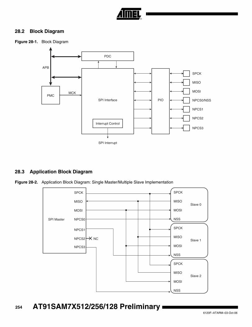
28.2 Block Diagram
Figure 28-1. Block Diagram
28.3 Application Block Diagram
Figure 28-2. Application Block Diagram: Single Master/Multiple Slave Implementation
SPI Interface
Interrupt Control
PIO
PDC
PMCMCK
SPI Interrupt
SPCK
MISO
MOSI
NPCS0/NSS
NPCS1
NPCS2
NPCS3
APB
SPI Master
SPCK
MISO
MOSI
NPCS0
NPCS1
NPCS2
SPCK
MISO
MOSI
NSS
Slave 0
SPCK
MISO
MOSI
NSS
Slave 1
SPCK
MISO
MOSI
NSS
Slave 2
NC
NPCS3
2546120F–ATARM–03-Oct-06
AT91SAM7X512/256/128 Preliminary

AT91SAM7X512/256/128 Preliminary
28.4 Signal Description
28.5 Product Dependencies
28.5.1 I/O Lines
The pins used for interfacing the compliant external devices may be multiplexed with PIO lines. The programmer must first program the PIO controllers to assign the SPI pins to their peripheral functions.
28.5.2 Power Management
The SPI may be clocked through the Power Management Controller (PMC), thus the program-mer must first configure the PMC to enable the SPI clock.
28.5.3 Interrupt
The SPI interface has an interrupt line connected to the Advanced Interrupt Controller (AIC). Handling the SPI interrupt requires programming the AIC before configuring the SPI.
Table 28-1. Signal Description
Pin Name Pin Description
Type
Master Slave
MISO Master In Slave Out Input Output
MOSI Master Out Slave In Output Input
SPCK Serial Clock Output Input
NPCS1-NPCS3 Peripheral Chip Selects Output Unused
NPCS0/NSS Peripheral Chip Select/Slave Select Output Input
2556120F–ATARM–03-Oct-06

28.6 Functional Description
28.6.1 Modes of Operation
The SPI operates in Master Mode or in Slave Mode.
Operation in Master Mode is programmed by writing at 1 the MSTR bit in the Mode Register. The pins NPCS0 to NPCS3 are all configured as outputs, the SPCK pin is driven, the MISO line is wired on the receiver input and the MOSI line driven as an output by the transmitter.
If the MSTR bit is written at 0, the SPI operates in Slave Mode. The MISO line is driven by the transmitter output, the MOSI line is wired on the receiver input, the SPCK pin is driven by the transmitter to synchronize the receiver. The NPCS0 pin becomes an input, and is used as a Slave Select signal (NSS). The pins NPCS1 to NPCS3 are not driven and can be used for other purposes.
The data transfers are identically programmable for both modes of operations. The baud rate generator is activated only in Master Mode.
28.6.2 Data Transfer
Four combinations of polarity and phase are available for data transfers. The clock polarity is programmed with the CPOL bit in the Chip Select Register. The clock phase is programmed with the NCPHA bit. These two parameters determine the edges of the clock signal on which data is driven and sampled. Each of the two parameters has two possible states, resulting in four possi-ble combinations that are incompatible with one another. Thus, a master/slave pair must use the same parameter pair values to communicate. If multiple slaves are used and fixed in different configurations, the master must reconfigure itself each time it needs to communicate with a dif-ferent slave.
Table 28-2 shows the four modes and corresponding parameter settings.
Figure 28-3 and Figure 28-4 show examples of data transfers.
Table 28-2. SPI Bus Protocol Mode
SPI Mode CPOL NCPHA
0 0 1
1 0 0
2 1 1
3 1 0
2566120F–ATARM–03-Oct-06
AT91SAM7X512/256/128 Preliminary

AT91SAM7X512/256/128 Preliminary
Figure 28-3. SPI Transfer Format (NCPHA = 1, 8 bits per transfer)
Figure 28-4. SPI Transfer Format (NCPHA = 0, 8 bits per transfer)
6
*
SPCK(CPOL = 0)
SPCK(CPOL = 1)
MOSI(from master)
MISO(from slave)
NSS(to slave)
SPCK cycle (for reference)
MSB
MSB
LSB
LSB
6
6
5
5
4
4
3
3
2
2
1
1
* Not defined, but normally MSB of previous character received.
1 2 3 4 5 7 86
*
SPCK(CPOL = 0)
SPCK(CPOL = 1)
1 2 3 4 5 7
MOSI(from master)
MISO(from slave)
NSS(to slave)
SPCK cycle (for reference) 8
MSB
MSB
LSB
LSB
6
6
5
5
4
4
3
3
1
1
* Not defined but normally LSB of previous character transmitted.
2
2
6
2576120F–ATARM–03-Oct-06
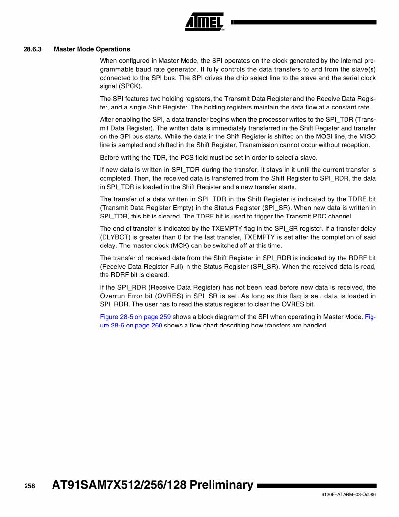
28.6.3 Master Mode Operations
When configured in Master Mode, the SPI operates on the clock generated by the internal pro-grammable baud rate generator. It fully controls the data transfers to and from the slave(s) connected to the SPI bus. The SPI drives the chip select line to the slave and the serial clock signal (SPCK).
The SPI features two holding registers, the Transmit Data Register and the Receive Data Regis-ter, and a single Shift Register. The holding registers maintain the data flow at a constant rate.
After enabling the SPI, a data transfer begins when the processor writes to the SPI_TDR (Trans-mit Data Register). The written data is immediately transferred in the Shift Register and transfer on the SPI bus starts. While the data in the Shift Register is shifted on the MOSI line, the MISO line is sampled and shifted in the Shift Register. Transmission cannot occur without reception.
Before writing the TDR, the PCS field must be set in order to select a slave.
If new data is written in SPI_TDR during the transfer, it stays in it until the current transfer is completed. Then, the received data is transferred from the Shift Register to SPI_RDR, the data in SPI_TDR is loaded in the Shift Register and a new transfer starts.
The transfer of a data written in SPI_TDR in the Shift Register is indicated by the TDRE bit (Transmit Data Register Empty) in the Status Register (SPI_SR). When new data is written in SPI_TDR, this bit is cleared. The TDRE bit is used to trigger the Transmit PDC channel.
The end of transfer is indicated by the TXEMPTY flag in the SPI_SR register. If a transfer delay (DLYBCT) is greater than 0 for the last transfer, TXEMPTY is set after the completion of said delay. The master clock (MCK) can be switched off at this time.
The transfer of received data from the Shift Register in SPI_RDR is indicated by the RDRF bit (Receive Data Register Full) in the Status Register (SPI_SR). When the received data is read, the RDRF bit is cleared.
If the SPI_RDR (Receive Data Register) has not been read before new data is received, the Overrun Error bit (OVRES) in SPI_SR is set. As long as this flag is set, data is loaded in SPI_RDR. The user has to read the status register to clear the OVRES bit.
Figure 28-5 on page 259 shows a block diagram of the SPI when operating in Master Mode. Fig-ure 28-6 on page 260 shows a flow chart describing how transfers are handled.
2586120F–ATARM–03-Oct-06
AT91SAM7X512/256/128 Preliminary
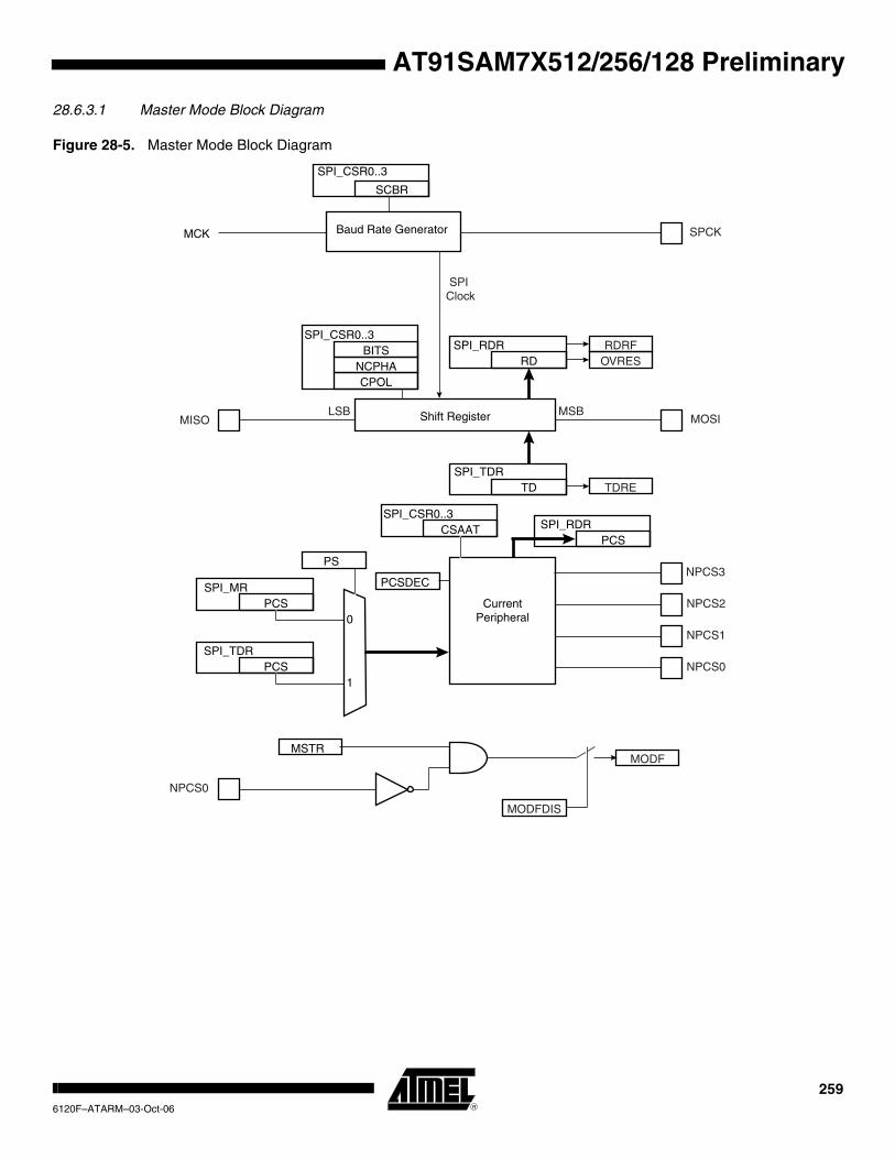
AT91SAM7X512/256/128 Preliminary
28.6.3.1 Master Mode Block Diagram
Figure 28-5. Master Mode Block Diagram
Shift Register
SPCK
MOSILSB MSB
MISO
SPI_RDRRD
SPI Clock
TDRESPI_TDR
TD
RDRFOVRES
SPI_CSR0..3
CPOLNCPHA
BITS
MCK Baud Rate Generator
SPI_CSR0..3
SCBR
NPCS3
NPCS0
NPCS2
NPCS1
NPCS0
0
1
PS
SPI_MRPCS
SPI_TDRPCS
MODF
CurrentPeripheral
SPI_RDRPCS
SPI_CSR0..3CSAAT
PCSDEC
MODFDIS
MSTR
2596120F–ATARM–03-Oct-06

28.6.3.2 Master Mode Flow Diagram
Figure 28-6. Master Mode Flow Diagram S
SPI Enable
CSAAT ?
PS ?
1
0
0
1
1
NPCS = SPI_TDR(PCS) NPCS = SPI_MR(PCS)
Delay DLYBS
Serializer = SPI_TDR(TD)TDRE = 1
Data Transfer
SPI_RDR(RD) = SerializerRDRF = 1
TDRE ?
NPCS = 0xF
Delay DLYBCS
Fixed peripheral
Variable peripheral
Delay DLYBCT
0
1CSAAT ?
0
TDRE ?1
0
PS ?0
1
SPI_TDR(PCS)= NPCS ?
no
yesSPI_MR(PCS)
= NPCS ?
no
NPCS = 0xF
Delay DLYBCS
NPCS = SPI_TDR(PCS)
NPCS = 0xF
Delay DLYBCS
NPCS = SPI_MR(PCS), SPI_TDR(PCS)
Fixed peripheral
Variable peripheral
- NPCS defines the current Chip Select- CSAAT, DLYBS, DLYBCT refer to the fields of the Chip Select Register corresponding to the Current Chip Select- When NPCS is 0xF, CSAAT is 0.
2606120F–ATARM–03-Oct-06
AT91SAM7X512/256/128 Preliminary

AT91SAM7X512/256/128 Preliminary
28.6.3.3 Clock Generation
The SPI Baud rate clock is generated by dividing the Master Clock (MCK), by a value between 1 and 255.
This allows a maximum operating baud rate at up to Master Clock and a minimum operating baud rate of MCK divided by 255.
Programming the SCBR field at 0 is forbidden. Triggering a transfer while SCBR is at 0 can lead to unpredictable results.
At reset, SCBR is 0 and the user has to program it at a valid value before performing the first transfer.
The divisor can be defined independently for each chip select, as it has to be programmed in the SCBR field of the Chip Select Registers. This allows the SPI to automatically adapt the baud rate for each interfaced peripheral without reprogramming.
28.6.3.4 Transfer Delays
Figure 28-7 shows a chip select transfer change and consecutive transfers on the same chip select. Three delays can be programmed to modify the transfer waveforms:
• The delay between chip selects, programmable only once for all the chip selects by writing the DLYBCS field in the Mode Register. Allows insertion of a delay between release of one chip select and before assertion of a new one.
• The delay before SPCK, independently programmable for each chip select by writing the field DLYBS. Allows the start of SPCK to be delayed after the chip select has been asserted.
• The delay between consecutive transfers, independently programmable for each chip select by writing the DLYBCT field. Allows insertion of a delay between two transfers occurring on the same chip select
These delays allow the SPI to be adapted to the interfaced peripherals and their speed and bus release time.
Figure 28-7. Programmable Delays
28.6.3.5 Peripheral Selection
The serial peripherals are selected through the assertion of the NPCS0 to NPCS3 signals. By default, all the NPCS signals are high before and after each transfer.
The peripheral selection can be performed in two different ways:
DLYBCS DLYBS DLYBCT DLYBCT
Chip Select 1
Chip Select 2
SPCK
2616120F–ATARM–03-Oct-06

• Fixed Peripheral Select: SPI exchanges data with only one peripheral
• Variable Peripheral Select: Data can be exchanged with more than one peripheral
Fixed Peripheral Select is activated by writing the PS bit to zero in SPI_MR (Mode Register). In this case, the current peripheral is defined by the PCS field in SPI_MR and the PCS field in the SPI_TDR has no effect.
Variable Peripheral Select is activated by setting PS bit to one. The PCS field in SPI_TDR is used to select the current peripheral. This means that the peripheral selection can be defined for each new data.
The Fixed Peripheral Selection allows buffer transfers with a single peripheral. Using the PDC is an optimal means, as the size of the data transfer between the memory and the SPI is either 8 bits or 16 bits. However, changing the peripheral selection requires the Mode Register to be reprogrammed.
The Variable Peripheral Selection allows buffer transfers with multiple peripherals without repro-gramming the Mode Register. Data written in SPI_TDR is 32 bits wide and defines the real data to be transmitted and the peripheral it is destined to. Using the PDC in this mode requires 32-bit wide buffers, with the data in the LSBs and the PCS and LASTXFER fields in the MSBs, how-ever the SPI still controls the number of bits (8 to16) to be transferred through MISO and MOSI lines with the chip select configuration registers. This is not the optimal means in term of mem-ory size for the buffers, but it provides a very effective means to exchange data with several peripherals without any intervention of the processor.
28.6.3.6 Peripheral Chip Select Decoding
The user can program the SPI to operate with up to 15 peripherals by decoding the four Chip Select lines, NPCS0 to NPCS3 with an external logic. This can be enabled by writing the PCS-DEC bit at 1 in the Mode Register (SPI_MR).
When operating without decoding, the SPI makes sure that in any case only one chip select line is activated, i.e. driven low at a time. If two bits are defined low in a PCS field, only the lowest numbered chip select is driven low.
When operating with decoding, the SPI directly outputs the value defined by the PCS field of either the Mode Register or the Transmit Data Register (depending on PS).
As the SPI sets a default value of 0xF on the chip select lines (i.e. all chip select lines at 1) when not processing any transfer, only 15 peripherals can be decoded.
The SPI has only four Chip Select Registers, not 15. As a result, when decoding is activated, each chip select defines the characteristics of up to four peripherals. As an example, SPI_CRS0 defines the characteristics of the externally decoded peripherals 0 to 3, corresponding to the PCS values 0x0 to 0x3. Thus, the user has to make sure to connect compatible peripherals on the decoded chip select lines 0 to 3, 4 to 7, 8 to 11 and 12 to 14.
28.6.3.7 Peripheral Deselection
When operating normally, as soon as the transfer of the last data written in SPI_TDR is com-pleted, the NPCS lines all rise. This might lead to runtime error if the processor is too long in responding to an interrupt, and thus might lead to difficulties for interfacing with some serial peripherals requiring the chip select line to remain active during a full set of transfers.
2626120F–ATARM–03-Oct-06
AT91SAM7X512/256/128 Preliminary

AT91SAM7X512/256/128 Preliminary
To facilitate interfacing with such devices, the Chip Select Register can be programmed with the CSAAT bit (Chip Select Active After Transfer) at 1. This allows the chip select lines to remain in their current state (low = active) until transfer to another peripheral is required.
Figure 28-8 shows different peripheral deselection cases and the effect of the CSAAT bit.
Figure 28-8. Peripheral Deselection
28.6.3.8 Mode Fault Detection
A mode fault is detected when the SPI is programmed in Master Mode and a low level is driven by an external master on the NPCS0/NSS signal. NPCS0, MOSI, MISO and SPCK must be con-figured in open drain through the PIO controller, so that external pull up resistors are needed to guarantee high level.
When a mode fault is detected, the MODF bit in the SPI_SR is set until the SPI_SR is read and the SPI is automatically disabled until re-enabled by writing the SPIEN bit in the SPI_CR (Con-trol Register) at 1.
By default, the Mode Fault detection circuitry is enabled. The user can disable Mode Fault detection by setting the MODFDIS bit in the SPI Mode Register (SPI_MR).
A
NPCS[0..3]
Write SPI_TDR
TDRE
NPCS[0..3]
Write SPI_TDR
TDRE
NPCS[0..3]
Write SPI_TDR
TDRE
DLYBCS
PCS = A
DLYBCS
DLYBCT
A
PCS = B
B
DLYBCS
PCS = A
DLYBCS
DLYBCT
A
PCS = B
B
DLYBCS
DLYBCT
PCS=A
A
DLYBCS
DLYBCT
A
PCS = A
AA
DLYBCT
A A
CSAAT = 0
DLYBCT
A A
CSAAT = 1
A
2636120F–ATARM–03-Oct-06

28.6.4 SPI Slave Mode
When operating in Slave Mode, the SPI processes data bits on the clock provided on the SPI clock pin (SPCK).
The SPI waits for NSS to go active before receiving the serial clock from an external master. When NSS falls, the clock is validated on the serializer, which processes the number of bits defined by the BITS field of the Chip Select Register 0 (SPI_CSR0). These bits are processed following a phase and a polarity defined respectively by the NCPHA and CPOL bits of the SPI_CSR0. Note that BITS, CPOL and NCPHA of the other Chip Select Registers have no effect when the SPI is programmed in Slave Mode.
The bits are shifted out on the MISO line and sampled on the MOSI line.
When all the bits are processed, the received data is transferred in the Receive Data Register and the RDRF bit rises. If RDRF is already high when the data is transferred, the Overrun bit rises and the data transfer to SPI_RDR is aborted.
When a transfer starts, the data shifted out is the data present in the Shift Register. If no data has been written in the Transmit Data Register (SPI_TDR), the last data received is transferred. If no data has been received since the last reset, all bits are transmitted low, as the Shift Regis-ter resets at 0.
When a first data is written in SPI_TDR, it is transferred immediately in the Shift Register and the TDRE bit rises. If new data is written, it remains in SPI_TDR until a transfer occurs, i.e. NSS falls and there is a valid clock on the SPCK pin. When the transfer occurs, the last data written in SPI_TDR is transferred in the Shift Register and the TDRE bit rises. This enables frequent updates of critical variables with single transfers.
Then, a new data is loaded in the Shift Register from the Transmit Data Register. In case no character is ready to be transmitted, i.e. no character has been written in SPI_TDR since the last load from SPI_TDR to the Shift Register, the Shift Register is not modified and the last received character is retransmitted.
Figure 28-9 shows a block diagram of the SPI when operating in Slave Mode.
Figure 28-9. Slave Mode Functional Block Diagram
Shift Register
SPCK
SPIENS
LSB MSB
NSS
MOSI
SPI_RDRRD
SPI Clock
TDRESPI_TDR
TD
RDRFOVRES
SPI_CSR0
CPOLNCPHA
BITS
SPIEN
SPIDIS
MISO
2646120F–ATARM–03-Oct-06
AT91SAM7X512/256/128 Preliminary

AT91SAM7X512/256/128 Preliminary
28.7 Serial Peripheral Interface (SPI) User Interface
Table 28-3. SPI Register Mapping
Offset Register Register Name Access Reset
0x00 Control Register SPI_CR Write-only ---
0x04 Mode Register SPI_MR Read/Write 0x0
0x08 Receive Data Register SPI_RDR Read-only 0x0
0x0C Transmit Data Register SPI_TDR Write-only ---
0x10 Status Register SPI_SR Read-only 0x000000F0
0x14 Interrupt Enable Register SPI_IER Write-only ---
0x18 Interrupt Disable Register SPI_IDR Write-only ---
0x1C Interrupt Mask Register SPI_IMR Read-only 0x0
0x20 - 0x2C Reserved
0x30 Chip Select Register 0 SPI_CSR0 Read/Write 0x0
0x34 Chip Select Register 1 SPI_CSR1 Read/Write 0x0
0x38 Chip Select Register 2 SPI_CSR2 Read/Write 0x0
0x3C Chip Select Register 3 SPI_CSR3 Read/Write 0x0
0x004C - 0x00F8 Reserved – – –
0x004C - 0x00FC Reserved – – –
0x100 - 0x124 Reserved for the PDC
2656120F–ATARM–03-Oct-06
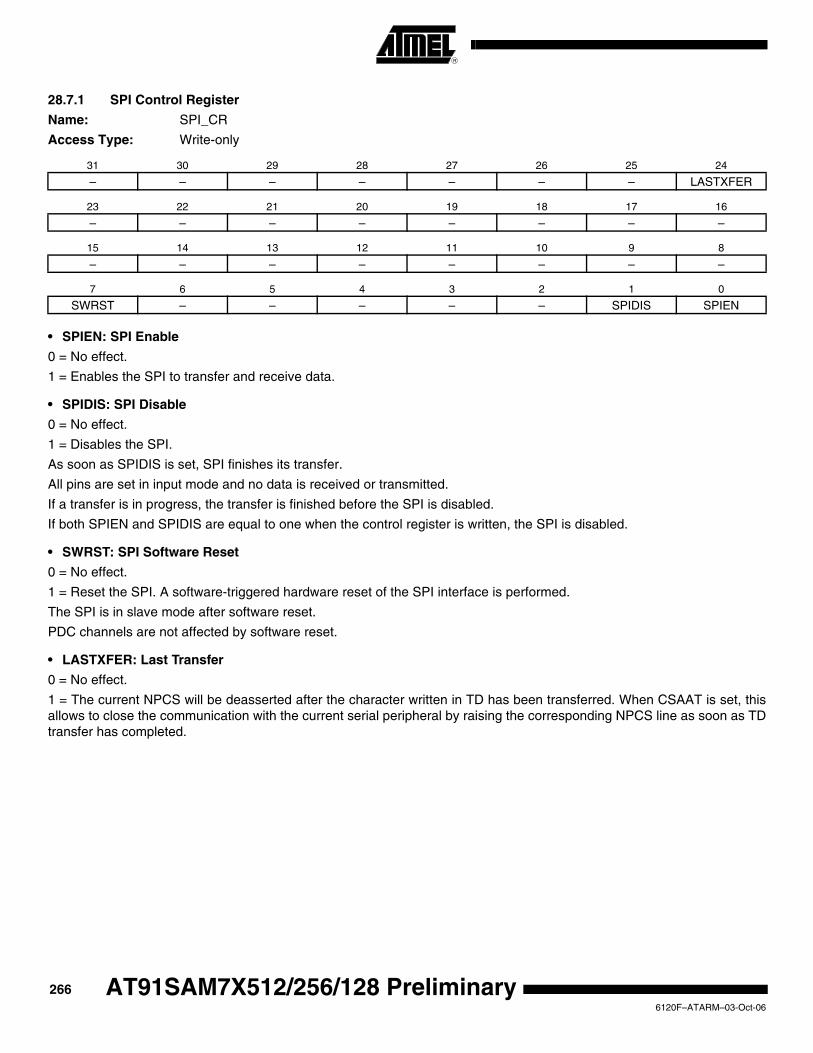
28.7.1 SPI Control Register
Name: SPI_CR
Access Type: Write-only
• SPIEN: SPI Enable
0 = No effect.
1 = Enables the SPI to transfer and receive data.
• SPIDIS: SPI Disable
0 = No effect.
1 = Disables the SPI.
As soon as SPIDIS is set, SPI finishes its transfer.
All pins are set in input mode and no data is received or transmitted.
If a transfer is in progress, the transfer is finished before the SPI is disabled.
If both SPIEN and SPIDIS are equal to one when the control register is written, the SPI is disabled.
• SWRST: SPI Software Reset
0 = No effect.
1 = Reset the SPI. A software-triggered hardware reset of the SPI interface is performed.
The SPI is in slave mode after software reset.
PDC channels are not affected by software reset.
• LASTXFER: Last Transfer
0 = No effect.
1 = The current NPCS will be deasserted after the character written in TD has been transferred. When CSAAT is set, this allows to close the communication with the current serial peripheral by raising the corresponding NPCS line as soon as TD transfer has completed.
31 30 29 28 27 26 25 24
– – – – – – – LASTXFER
23 22 21 20 19 18 17 16
– – – – – – – –
15 14 13 12 11 10 9 8
– – – – – – – –
7 6 5 4 3 2 1 0
SWRST – – – – – SPIDIS SPIEN
2666120F–ATARM–03-Oct-06
AT91SAM7X512/256/128 Preliminary
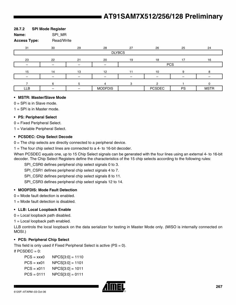
AT91SAM7X512/256/128 Preliminary
28.7.2 SPI Mode Register
Name: SPI_MR
Access Type: Read/Write
• MSTR: Master/Slave Mode
0 = SPI is in Slave mode.
1 = SPI is in Master mode.
• PS: Peripheral Select
0 = Fixed Peripheral Select.
1 = Variable Peripheral Select.
• PCSDEC: Chip Select Decode
0 = The chip selects are directly connected to a peripheral device.
1 = The four chip select lines are connected to a 4- to 16-bit decoder.
When PCSDEC equals one, up to 15 Chip Select signals can be generated with the four lines using an external 4- to 16-bit decoder. The Chip Select Registers define the characteristics of the 15 chip selects according to the following rules:
SPI_CSR0 defines peripheral chip select signals 0 to 3.
SPI_CSR1 defines peripheral chip select signals 4 to 7.
SPI_CSR2 defines peripheral chip select signals 8 to 11.
SPI_CSR3 defines peripheral chip select signals 12 to 14.
• MODFDIS: Mode Fault Detection
0 = Mode fault detection is enabled.
1 = Mode fault detection is disabled.
• LLB: Local Loopback Enable
0 = Local loopback path disabled.
1 = Local loopback path enabled.
LLB controls the local loopback on the data serializer for testing in Master Mode only. (MISO is internally connected on MOSI.)
• PCS: Peripheral Chip Select
This field is only used if Fixed Peripheral Select is active (PS = 0).
If PCSDEC = 0:
PCS = xxx0 NPCS[3:0] = 1110
PCS = xx01 NPCS[3:0] = 1101
PCS = x011 NPCS[3:0] = 1011
PCS = 0111 NPCS[3:0] = 0111
31 30 29 28 27 26 25 24
DLYBCS
23 22 21 20 19 18 17 16
– – – – PCS
15 14 13 12 11 10 9 8
– – – – – – – –
7 6 5 4 3 2 1 0
LLB – – MODFDIS PCSDEC PS MSTR
2676120F–ATARM–03-Oct-06

PCS = 1111 forbidden (no peripheral is selected)
(x = don’t care)
If PCSDEC = 1:
NPCS[3:0] output signals = PCS.
• DLYBCS: Delay Between Chip Selects
This field defines the delay from NPCS inactive to the activation of another NPCS. The DLYBCS time guarantees non-over-lapping chip selects and solves bus contentions in case of peripherals having long data float times.
If DLYBCS is less than or equal to six, six MCK periods will be inserted by default.
Otherwise, the following equation determines the delay:
Delay Between Chip Selects DLYBCSMCK
-----------------------=
2686120F–ATARM–03-Oct-06
AT91SAM7X512/256/128 Preliminary
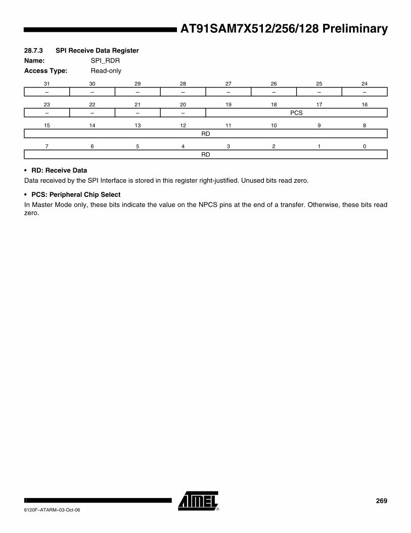
AT91SAM7X512/256/128 Preliminary
28.7.3 SPI Receive Data Register
Name: SPI_RDR
Access Type: Read-only
• RD: Receive Data
Data received by the SPI Interface is stored in this register right-justified. Unused bits read zero.
• PCS: Peripheral Chip Select
In Master Mode only, these bits indicate the value on the NPCS pins at the end of a transfer. Otherwise, these bits read zero.
31 30 29 28 27 26 25 24
– – – – – – – –
23 22 21 20 19 18 17 16
– – – – PCS
15 14 13 12 11 10 9 8
RD
7 6 5 4 3 2 1 0
RD
2696120F–ATARM–03-Oct-06
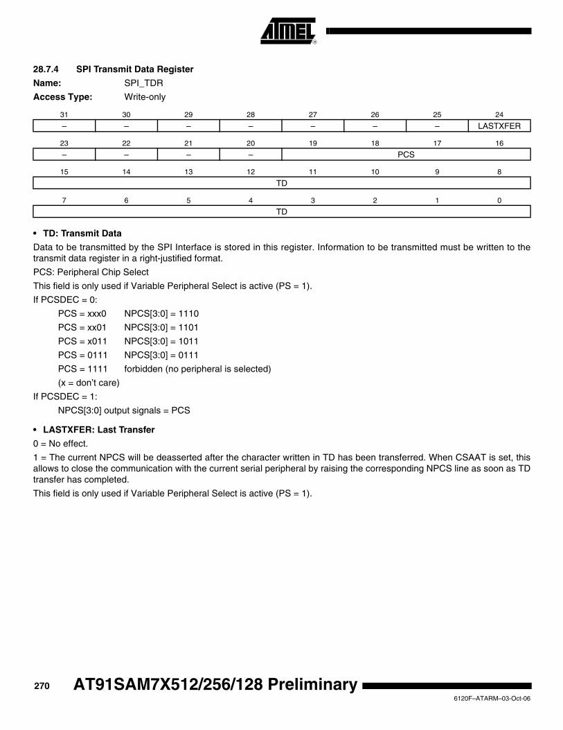
28.7.4 SPI Transmit Data Register
Name: SPI_TDR
Access Type: Write-only
• TD: Transmit Data
Data to be transmitted by the SPI Interface is stored in this register. Information to be transmitted must be written to the transmit data register in a right-justified format.
PCS: Peripheral Chip Select
This field is only used if Variable Peripheral Select is active (PS = 1).
If PCSDEC = 0:
PCS = xxx0 NPCS[3:0] = 1110
PCS = xx01 NPCS[3:0] = 1101
PCS = x011 NPCS[3:0] = 1011
PCS = 0111 NPCS[3:0] = 0111
PCS = 1111 forbidden (no peripheral is selected)
(x = don’t care)
If PCSDEC = 1:
NPCS[3:0] output signals = PCS
• LASTXFER: Last Transfer
0 = No effect.
1 = The current NPCS will be deasserted after the character written in TD has been transferred. When CSAAT is set, this allows to close the communication with the current serial peripheral by raising the corresponding NPCS line as soon as TD transfer has completed.
This field is only used if Variable Peripheral Select is active (PS = 1).
31 30 29 28 27 26 25 24
– – – – – – – LASTXFER
23 22 21 20 19 18 17 16
– – – – PCS
15 14 13 12 11 10 9 8
TD
7 6 5 4 3 2 1 0
TD
2706120F–ATARM–03-Oct-06
AT91SAM7X512/256/128 Preliminary

AT91SAM7X512/256/128 Preliminary
28.7.5 SPI Status Register
Name: SPI_SR
Access Type: Read-only
• RDRF: Receive Data Register Full
0 = No data has been received since the last read of SPI_RDR
1 = Data has been received and the received data has been transferred from the serializer to SPI_RDR since the last read of SPI_RDR.
• TDRE: Transmit Data Register Empty
0 = Data has been written to SPI_TDR and not yet transferred to the serializer.
1 = The last data written in the Transmit Data Register has been transferred to the serializer.
TDRE equals zero when the SPI is disabled or at reset. The SPI enable command sets this bit to one.
• MODF: Mode Fault Error
0 = No Mode Fault has been detected since the last read of SPI_SR.
1 = A Mode Fault occurred since the last read of the SPI_SR.
• OVRES: Overrun Error Status
0 = No overrun has been detected since the last read of SPI_SR.
1 = An overrun has occurred since the last read of SPI_SR.
An overrun occurs when SPI_RDR is loaded at least twice from the serializer since the last read of the SPI_RDR.
• ENDRX: End of RX buffer
0 = The Receive Counter Register has not reached 0 since the last write in SPI_RCR(1) or SPI_RNCR(1).
1 = The Receive Counter Register has reached 0 since the last write in SPI_RCR(1) or SPI_RNCR(1).
• ENDTX: End of TX buffer
0 = The Transmit Counter Register has not reached 0 since the last write in SPI_TCR(1) or SPI_TNCR(1).
1 = The Transmit Counter Register has reached 0 since the last write in SPI_TCR(1) or SPI_TNCR(1).
• RXBUFF: RX Buffer Full
0 = SPI_RCR(1) or SPI_RNCR(1) has a value other than 0.
1 = Both SPI_RCR(1) and SPI_RNCR(1) have a value of 0.
• TXBUFE: TX Buffer Empty
0 = SPI_TCR(1) or SPI_TNCR(1) has a value other than 0.
1 = Both SPI_TCR(1) and SPI_TNCR(1) have a value of 0.
• NSSR: NSS Rising
31 30 29 28 27 26 25 24
– – – – – – – –
23 22 21 20 19 18 17 16
– – – – – – – SPIENS
15 14 13 12 11 10 9 8
– – – – – – TXEMPTY NSSR
7 6 5 4 3 2 1 0
TXBUFE RXBUFF ENDTX ENDRX OVRES MODF TDRE RDRF
2716120F–ATARM–03-Oct-06
0 = No rising edge detected on NSS pin since last read.
1 = A rising edge occurred on NSS pin since last read.
• TXEMPTY: Transmission Registers Empty
0 = As soon as data is written in SPI_TDR.
1 = SPI_TDR and internal shifter are empty. If a transfer delay has been defined, TXEMPTY is set after the completion of such delay.
• SPIENS: SPI Enable Status
0 = SPI is disabled.
1 = SPI is enabled.
Note: 1. SPI_RCR, SPI_RNCR, SPI_TCR, SPI_TNCR are physically located in the PDC.
2726120F–ATARM–03-Oct-06
AT91SAM7X512/256/128 Preliminary

AT91SAM7X512/256/128 Preliminary
28.7.6 SPI Interrupt Enable Register
Name: SPI_IER
Access Type: Write-only
• RDRF: Receive Data Register Full Interrupt Enable
• TDRE: SPI Transmit Data Register Empty Interrupt Enable
• MODF: Mode Fault Error Interrupt Enable
• OVRES: Overrun Error Interrupt Enable
• ENDRX: End of Receive Buffer Interrupt Enable
• ENDTX: End of Transmit Buffer Interrupt Enable
• RXBUFF: Receive Buffer Full Interrupt Enable
• TXBUFE: Transmit Buffer Empty Interrupt Enable
• TXEMPTY: Transmission Registers Empty Enable
• NSSR: NSS Rising Interrupt Enable
0 = No effect.
1 = Enables the corresponding interrupt.
31 30 29 28 27 26 25 24
– – – – – – – –
23 22 21 20 19 18 17 16
– – – – – – – –
15 14 13 12 11 10 9 8
– – – – – – TXEMPTY NSSR
7 6 5 4 3 2 1 0
TXBUFE RXBUFF ENDTX ENDRX OVRES MODF TDRE RDRF
2736120F–ATARM–03-Oct-06

28.7.7 SPI Interrupt Disable Register
Name: SPI_IDR
Access Type: Write-only
• RDRF: Receive Data Register Full Interrupt Disable
• TDRE: SPI Transmit Data Register Empty Interrupt Disable
• MODF: Mode Fault Error Interrupt Disable
• OVRES: Overrun Error Interrupt Disable
• ENDRX: End of Receive Buffer Interrupt Disable
• ENDTX: End of Transmit Buffer Interrupt Disable
• RXBUFF: Receive Buffer Full Interrupt Disable
• TXBUFE: Transmit Buffer Empty Interrupt Disable
• TXEMPTY: Transmission Registers Empty Disable
• NSSR: NSS Rising Interrupt Disable
0 = No effect.
1 = Disables the corresponding interrupt.
31 30 29 28 27 26 25 24
– – – – – – – –
23 22 21 20 19 18 17 16
– – – – – – – –
15 14 13 12 11 10 9 8
– – – – – – TXEMPTY NSSR
7 6 5 4 3 2 1 0
TXBUFE RXBUFF ENDTX ENDRX OVRES MODF TDRE RDRF
2746120F–ATARM–03-Oct-06
AT91SAM7X512/256/128 Preliminary

AT91SAM7X512/256/128 Preliminary
28.7.8 SPI Interrupt Mask Register
Name: SPI_IMR
Access Type: Read-only
• RDRF: Receive Data Register Full Interrupt Mask
• TDRE: SPI Transmit Data Register Empty Interrupt Mask
• MODF: Mode Fault Error Interrupt Mask
• OVRES: Overrun Error Interrupt Mask
• ENDRX: End of Receive Buffer Interrupt Mask
• ENDTX: End of Transmit Buffer Interrupt Mask
• RXBUFF: Receive Buffer Full Interrupt Mask
• TXBUFE: Transmit Buffer Empty Interrupt Mask
• TXEMPTY: Transmission Registers Empty Mask
• NSSR: NSS Rising Interrupt Mask
0 = The corresponding interrupt is not enabled.
1 = The corresponding interrupt is enabled.
31 30 29 28 27 26 25 24
– – – – – – – –
23 22 21 20 19 18 17 16
– – – – – – – –
15 14 13 12 11 10 9 8
– – – – – – TXEMPTY NSSR
7 6 5 4 3 2 1 0
TXBUFE RXBUFF ENDTX ENDRX OVRES MODF TDRE RDRF
2756120F–ATARM–03-Oct-06

28.7.9 SPI Chip Select Register
Name: SPI_CSR0... SPI_CSR3
Access Type: Read/Write
• CPOL: Clock Polarity
0 = The inactive state value of SPCK is logic level zero.
1 = The inactive state value of SPCK is logic level one.
CPOL is used to determine the inactive state value of the serial clock (SPCK). It is used with NCPHA to produce the required clock/data relationship between master and slave devices.• NCPHA: Clock Phase
0 = Data is changed on the leading edge of SPCK and captured on the following edge of SPCK.
1 = Data is captured on the leading edge of SPCK and changed on the following edge of SPCK.
NCPHA determines which edge of SPCK causes data to change and which edge causes data to be captured. NCPHA is used with CPOL to produce the required clock/data relationship between master and slave devices.• CSAAT: Chip Select Active After Transfer
0 = The Peripheral Chip Select Line rises as soon as the last transfer is achieved.
1 = The Peripheral Chip Select does not rise after the last transfer is achieved. It remains active until a new transfer is requested on a different chip select. • BITS: Bits Per Transfer
The BITS field determines the number of data bits transferred. Reserved values should not be used.
31 30 29 28 27 26 25 24
DLYBCT
23 22 21 20 19 18 17 16
DLYBS
15 14 13 12 11 10 9 8
SCBR
7 6 5 4 3 2 1 0
BITS CSAAT – NCPHA CPOL
BITS Bits Per Transfer0000 8
0001 9
0010 100011 11
0100 12
0101 130110 14
0111 15
1000 161001 Reserved
1010 Reserved
1011 Reserved
1100 Reserved1101 Reserved
1110 Reserved
1111 Reserved
2766120F–ATARM–03-Oct-06
AT91SAM7X512/256/128 Preliminary

AT91SAM7X512/256/128 Preliminary
• SCBR: Serial Clock Baud Rate
In Master Mode, the SPI Interface uses a modulus counter to derive the SPCK baud rate from the Master Clock MCK. The Baud rate is selected by writing a value from 1 to 255 in the SCBR field. The following equations determine the SPCK baud rate:
Programming the SCBR field at 0 is forbidden. Triggering a transfer while SCBR is at 0 can lead to unpredictable results.
At reset, SCBR is 0 and the user has to program it at a valid value before performing the first transfer.
• DLYBS: Delay Before SPCK
This field defines the delay from NPCS valid to the first valid SPCK transition.
When DLYBS equals zero, the NPCS valid to SPCK transition is 1/2 the SPCK clock period.
Otherwise, the following equations determine the delay:
• DLYBCT: Delay Between Consecutive Transfers
This field defines the delay between two consecutive transfers with the same peripheral without removing the chip select. The delay is always inserted after each transfer and before removing the chip select if needed.
When DLYBCT equals zero, no delay between consecutive transfers is inserted and the clock keeps its duty cycle over the character transfers.
Otherwise, the following equation determines the delay:
SPCK Baudrate MCKSCBR---------------=
Delay Before SPCK DLYBSMCK
-------------------=
Delay Between Consecutive Transfers 32 DLYBCT×MCK
------------------------------------=
2776120F–ATARM–03-Oct-06

2786120F–ATARM–03-Oct-06
AT91SAM7X512/256/128 Preliminary

AT91SAM7X512/256/128 Preliminary
29. Two-wire Interface (TWI)
29.1 Overview
The Two-wire Interface (TWI) interconnects components on a unique two-wire bus, made up of one clock line and one data line with speeds of up to 400 Kbits per second, based on a byte-ori-ented transfer format. It can be used with any Atmel two-wire bus Serial EEPROM. The TWI is programmable as a master with sequential or single-byte access. A configurable baud rate gen-erator permits the output data rate to be adapted to a wide range of core clock frequencies.
29.2 Block Diagram
Figure 29-1. Block Diagram
29.3 Application Block Diagram
Figure 29-2. Application Block Diagram
APB Bridge
PMC MCK
Two-wireInterface
PIO
AICTWI
Interrupt
TWCK
TWD
Host withTWI
Interface
TWD
TWCK
AT24LC16U1
AT24LC16U2
LCD ControllerU3
Slave 1 Slave 2 Slave 3
R R
VDD
2796120F–ATARM–03-Oct-06

29.4 Product Dependencies
29.4.1 I/O Lines Description
29.4.2 I/O Lines
Both TWD and TWCK are bi-directional lines, connected to a positive supply voltage via a cur-rent source or pull-up resistor (see Figure 29-2 on page 279). When the bus is free, both lines are high. The output stages of devices connected to the bus must have an open-drain or open-collector to perform the wired-AND function.
TWD and TWCK pins may be multiplexed with PIO lines. To enable the TWI, the programmer must perform the following steps:
• Program the PIO controller to:
– Dedicate TWD and TWCK as peripheral lines.
– Define TWD and TWCK as open-drain.
29.4.3 Power Management
• Enable the peripheral clock.
The TWI interface may be clocked through the Power Management Controller (PMC), thus the programmer must first configure the PMC to enable the TWI clock.
29.4.4 Interrupt
The TWI interface has an interrupt line connected to the Advanced Interrupt Controller (AIC). In order to handle interrupts, the AIC must be programmed before configuring the TWI.
Table 29-1. I/O Lines Description
Pin Name Pin Description Type
TWD Two-wire Serial Data Input/Output
TWCK Two-wire Serial Clock Input/Output
2806120F–ATARM–03-Oct-06
AT91SAM7X512/256/128 Preliminary
AT91SAM7X512/256/128 Preliminary
29.5 Functional Description
29.5.1 Transfer format
The data put on the TWD line must be 8 bits long. Data is transferred MSB first; each byte must be followed by an acknowledgement. The number of bytes per transfer is unlimited (see Figure 29-4 on page 281).
Each transfer begins with a START condition and terminates with a STOP condition (see Figure 29-3 on page 281).
• A high-to-low transition on the TWD line while TWCK is high defines the START condition.
• A low-to-high transition on the TWD line while TWCK is high defines a STOP condition.
Figure 29-3. START and STOP Conditions
Figure 29-4. Transfer Format
29.5.2 Modes of Operation
The TWI has two modes of operation:
• Master transmitter mode
• Master receiver mode
The TWI Control Register (TWI_CR) allows configuration of the interface in Master Mode. In this mode, it generates the clock according to the value programmed in the Clock Waveform Gener-ator Register (TWI_CWGR). This register defines the TWCK signal completely, enabling the interface to be adapted to a wide range of clocks.
29.5.3 Transmitting Data
After the master initiates a Start condition, it sends a 7-bit slave address, configured in the Mas-ter Mode register (DADR in TWI_MMR), to notify the slave device. The bit following the slave address indicates the transfer direction (write or read). If this bit is 0, it indicates a write operation (transmit operation). If the bit is 1, it indicates a request for data read (receive operation).
The TWI transfers require the slave to acknowledge each received byte. During the acknowl-edge clock pulse, the master releases the data line (HIGH), enabling the slave to pull it down in order to generate the acknowledge. The master polls the data line during this clock pulse and
TWD
TWCK
Start Stop
TWD
TWCK
Start Address R/W Ack Data Ack Data Ack Stop
2816120F–ATARM–03-Oct-06

sets the NAK bit in the status register if the slave does not acknowledge the byte. As with the other status bits, an interrupt can be generated if enabled in the interrupt enable register (TWI_IER). After writing in the transmit-holding register (TWI_THR), setting the START bit in the control register starts the transmission. The data is shifted in the internal shifter and when an acknowledge is detected, the TXRDY bit is set until a new write in the TWI_THR (see Figure 29-6 below). The master generates a stop condition to end the transfer.
The read sequence begins by setting the START bit. When the RXRDY bit is set in the status register, a character has been received in the receive-holding register (TWI_RHR). The RXRDY bit is reset when reading the TWI_RHR.
The TWI interface performs various transfer formats (7-bit slave address, 10-bit slave address). The three internal address bytes are configurable through the Master Mode register (TWI_MMR). If the slave device supports only a 7-bit address, IADRSZ must be set to 0. For a slave address higher than 7 bits, the user must configure the address size (IADRSZ) and set the other slave address bits in the internal address register (TWI_IADR).
Figure 29-5. Master Write with One, Two or Three Bytes Internal Address and One Data Byte
Figure 29-6. Master Write with One Byte Internal Address and Multiple Data Bytes
Figure 29-7. Master Read with One, Two or Three Bytes Internal Address and One Data Byte
S DADR W A IADR(23:16) A IADR(15:8) A IADR(7:0) A DATA A P
S DADR W A IADR(15:8) A IADR(7:0) A PDATA A
A IADR(7:0) A PDATA AS DADR W
TWD
Three bytes internal address
Two bytes internal address
One byte internal address
TWD
TWD
A IADR(7:0) A DATA AS DADR W DATA A PDATA A
TXCOMP
TXRDY
Write THR
Write THR Write THR Write THR
TWD
S DADR W A IADR(23:16) A IADR(15:8) A IADR(7:0) A
S DADR W A IADR(15:8) A IADR(7:0) A
A IADR(7:0) AS DADR W
DATA N P
S DADR R A
S DADR R A DATA N P
S DADR R A DATA N P
TWD
TWD
TWD
Three bytes internal address
Two bytes internal address
One byte internal address
2826120F–ATARM–03-Oct-06
AT91SAM7X512/256/128 Preliminary
AT91SAM7X512/256/128 Preliminary
Figure 29-8. Master Read with One Byte Internal Address and Multiple Data Bytes
• S = Start
• P = Stop
• W = Write
• R = Read
• A = Acknowledge
• N = Not Acknowledge
• DADR= Device Address
• IADR = Internal Address
Figure 29-9 below shows a byte write to an Atmel AT24LC512 EEPROM. This demonstrates the use of internal addresses to access the device.
Figure 29-9. Internal Address Usage
A IADR(7:0) AS DADR W S DADR R A DATA A DATA N P
TXCOMP
Write START Bit
RXRDY
Write STOP Bit
Read RHR Read RHR
TWD
START
MSB
DeviceAddress
0
LSB
R/
W
ACK
MSB
WRITE
ACK
ACK
LSB
ACK
FIRSTWORD ADDRESS
SECONDWORD ADDRESS DATA
STOP
2836120F–ATARM–03-Oct-06

29.5.4 Read/Write Flowcharts
The following flowcharts shown in Figure 29-10 and in Figure 29-11 on page 285 give examples for read and write operations in Master Mode. A polling or interrupt method can be used to check the status bits. The interrupt method requires that the interrupt enable register (TWI_IER) be configured first.
Figure 29-10. TWI Write in Master Mode
Set TWI clock:TWI_CWGR = clock
Set the control register:- Master enable
TWI_CR = MSEN
Set the Master Mode register:- Device slave address- Internal address size- Transfer direction bit
Write ==> bit MREAD = 0
Internal address size = 0?
Load transmit registerTWI_THR = Data to send
Start the transferTWI_CR = START
Stop the transferTWI_CR = STOP
Read status register
TXRDY = 0?
Data to send?
Read status register
TXCOMP = 0?
END
START
Set theinternal addressTWI_IADR = address
Yes
TWI_THR = data to send
Yes
Yes
Yes
2846120F–ATARM–03-Oct-06
AT91SAM7X512/256/128 Preliminary
AT91SAM7X512/256/128 Preliminary
Figure 29-11. TWI Read in Master Mode
Set TWI clock:TWI_CWGR = clock
Set the control register:- Master enable- Slave disable
TWI_CR = MSEN
Set the Master Mode register:- Device slave address- Internal address size- Transfer direction bit
Read ==> bit MREAD = 0
Internal address size = 0?
Start the transferTWI_CR = START
Stop the transferTWI_CR = STOP
Read status register
RXRDY = 0?
Data to read?
Read status register
TXCOMP = 0?
END
START
Set the internal addressTWI_IADR = address
Yes
Yes
Yes
Yes
2856120F–ATARM–03-Oct-06

29.6 TWI User Interface
29.6.1 Register Mapping
Table 29-2. Two-wire Interface (TWI) User Interface
Offset Register Name Access Reset Value
0x0000 Control Register TWI_CR Write-only N/A
0x0004 Master Mode Register TWI_MMR Read/Write 0x0000
0x0008 Reserved - - -
0x000C Internal Address Register TWI_IADR Read/Write 0x0000
0x0010 Clock Waveform Generator Register TWI_CWGR Read/Write 0x0000
0x0020 Status Register TWI_SR Read-only 0x0008
0x0024 Interrupt Enable Register TWI_IER Write-only N/A
0x0028 Interrupt Disable Register TWI_IDR Write-only N/A
0x002C Interrupt Mask Register TWI_IMR Read-only 0x0000
0x0030 Receive Holding Register TWI_RHR Read-only 0x0000
0x0034 Transmit Holding Register TWI_THR Read/Write 0x0000
0x0038 - 0x00FC Reserved – – –
2866120F–ATARM–03-Oct-06
AT91SAM7X512/256/128 Preliminary
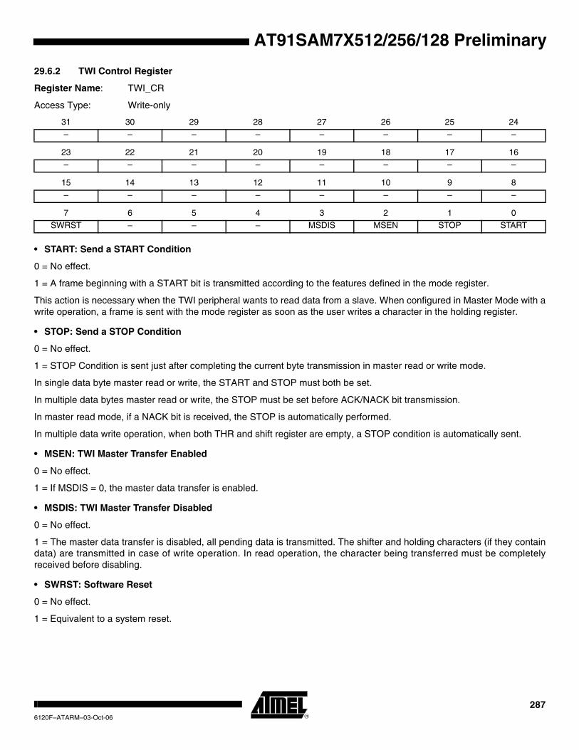
AT91SAM7X512/256/128 Preliminary
29.6.2 TWI Control Register
Register Name: TWI_CR
Access Type: Write-only
• START: Send a START Condition
0 = No effect.
1 = A frame beginning with a START bit is transmitted according to the features defined in the mode register.
This action is necessary when the TWI peripheral wants to read data from a slave. When configured in Master Mode with a write operation, a frame is sent with the mode register as soon as the user writes a character in the holding register.
• STOP: Send a STOP Condition
0 = No effect.
1 = STOP Condition is sent just after completing the current byte transmission in master read or write mode.
In single data byte master read or write, the START and STOP must both be set.
In multiple data bytes master read or write, the STOP must be set before ACK/NACK bit transmission.
In master read mode, if a NACK bit is received, the STOP is automatically performed.
In multiple data write operation, when both THR and shift register are empty, a STOP condition is automatically sent.
• MSEN: TWI Master Transfer Enabled
0 = No effect.
1 = If MSDIS = 0, the master data transfer is enabled.
• MSDIS: TWI Master Transfer Disabled
0 = No effect.
1 = The master data transfer is disabled, all pending data is transmitted. The shifter and holding characters (if they contain data) are transmitted in case of write operation. In read operation, the character being transferred must be completely received before disabling.
• SWRST: Software Reset
0 = No effect.
1 = Equivalent to a system reset.
31 30 29 28 27 26 25 24– – – – – – – –
23 22 21 20 19 18 17 16
– – – – – – – –
15 14 13 12 11 10 9 8– – – – – – – –
7 6 5 4 3 2 1 0
SWRST – – – MSDIS MSEN STOP START
2876120F–ATARM–03-Oct-06
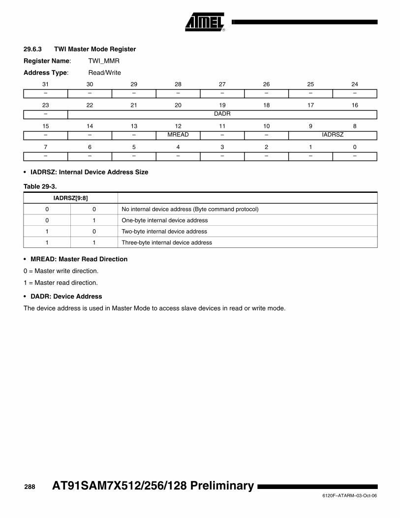
29.6.3 TWI Master Mode Register
Register Name: TWI_MMR
Address Type: Read/Write
• IADRSZ: Internal Device Address Size
• MREAD: Master Read Direction
0 = Master write direction.
1 = Master read direction.
• DADR: Device Address
The device address is used in Master Mode to access slave devices in read or write mode.
31 30 29 28 27 26 25 24– – – – – – – –
23 22 21 20 19 18 17 16
– DADR
15 14 13 12 11 10 9 8– – – MREAD – – IADRSZ
7 6 5 4 3 2 1 0
– – – – – – – –
Table 29-3.
IADRSZ[9:8]
0 0 No internal device address (Byte command protocol)
0 1 One-byte internal device address
1 0 Two-byte internal device address
1 1 Three-byte internal device address
2886120F–ATARM–03-Oct-06
AT91SAM7X512/256/128 Preliminary

AT91SAM7X512/256/128 Preliminary
29.6.4 TWI Internal Address Register
Register Name: TWI_IADR
Access Type: Read/Write
• IADR: Internal Address
0, 1, 2 or 3 bytes depending on IADRSZ.
– Low significant byte address in 10-bit mode addresses.
31 30 29 28 27 26 25 24– – – – – – – –
23 22 21 20 19 18 17 16
IADR
15 14 13 12 11 10 9 8IADR
7 6 5 4 3 2 1 0
IADR
2896120F–ATARM–03-Oct-06
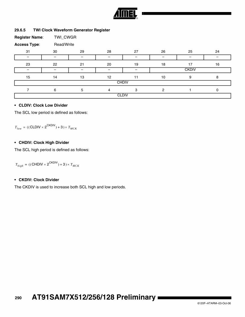
29.6.5 TWI Clock Waveform Generator Register
Register Name: TWI_CWGR
Access Type: Read/Write
• CLDIV: Clock Low Divider
The SCL low period is defined as follows:
• CHDIV: Clock High Divider
The SCL high period is defined as follows:
• CKDIV: Clock Divider
The CKDIV is used to increase both SCL high and low periods.
31 30 29 28 27 26 25 24– – – – – – – –
23 22 21 20 19 18 17 16
– – – – – CKDIV
15 14 13 12 11 10 9 8CHDIV
7 6 5 4 3 2 1 0
CLDIV
Tlow CLDIV( 2CKDIV×( ) 3 )+ TMCK×=
Thigh CHDIV( 2CKDIV×( ) 3 )+ TMCK×=
2906120F–ATARM–03-Oct-06
AT91SAM7X512/256/128 Preliminary
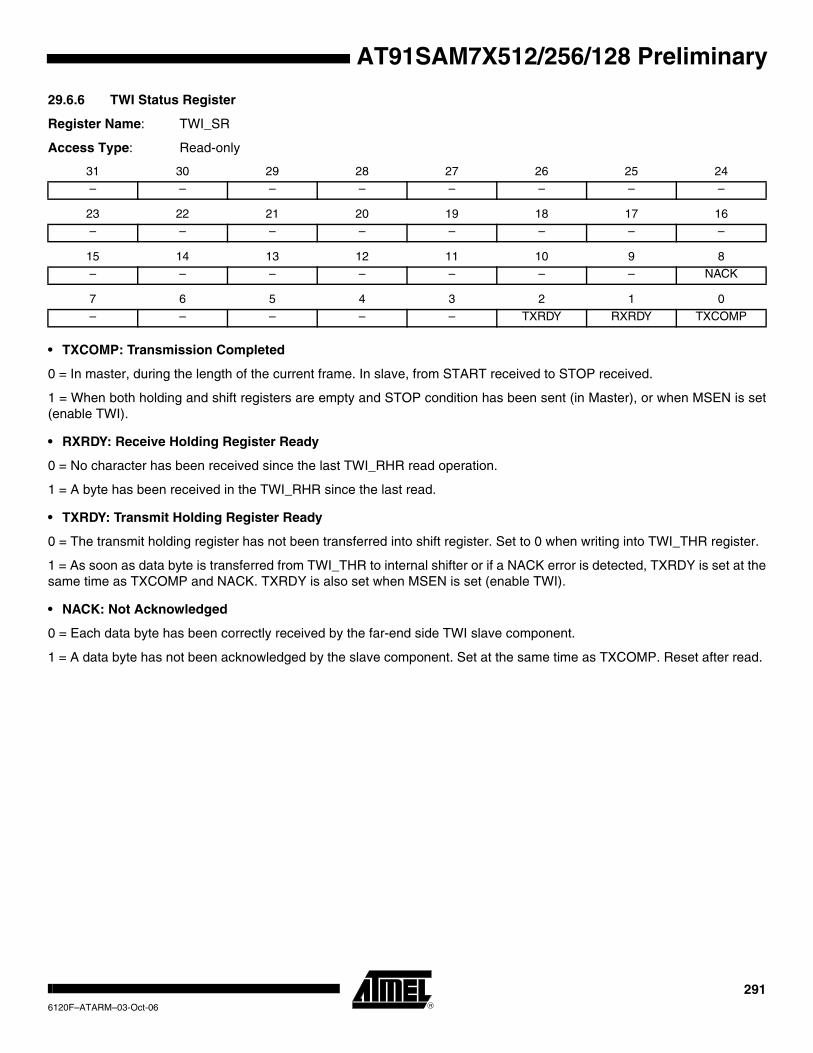
AT91SAM7X512/256/128 Preliminary
29.6.6 TWI Status Register
Register Name: TWI_SR
Access Type: Read-only
• TXCOMP: Transmission Completed
0 = In master, during the length of the current frame. In slave, from START received to STOP received.
1 = When both holding and shift registers are empty and STOP condition has been sent (in Master), or when MSEN is set (enable TWI).
• RXRDY: Receive Holding Register Ready
0 = No character has been received since the last TWI_RHR read operation.
1 = A byte has been received in the TWI_RHR since the last read.
• TXRDY: Transmit Holding Register Ready
0 = The transmit holding register has not been transferred into shift register. Set to 0 when writing into TWI_THR register.
1 = As soon as data byte is transferred from TWI_THR to internal shifter or if a NACK error is detected, TXRDY is set at the same time as TXCOMP and NACK. TXRDY is also set when MSEN is set (enable TWI).
• NACK: Not Acknowledged
0 = Each data byte has been correctly received by the far-end side TWI slave component.
1 = A data byte has not been acknowledged by the slave component. Set at the same time as TXCOMP. Reset after read.
31 30 29 28 27 26 25 24– – – – – – – –
23 22 21 20 19 18 17 16
– – – – – – – –
15 14 13 12 11 10 9 8– – – – – – – NACK
7 6 5 4 3 2 1 0
– – – – – TXRDY RXRDY TXCOMP
2916120F–ATARM–03-Oct-06
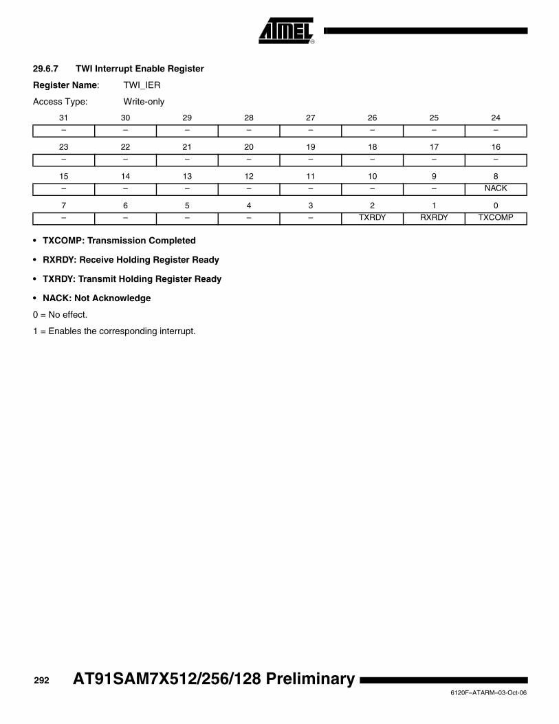
29.6.7 TWI Interrupt Enable Register
Register Name: TWI_IER
Access Type: Write-only
• TXCOMP: Transmission Completed
• RXRDY: Receive Holding Register Ready
• TXRDY: Transmit Holding Register Ready
• NACK: Not Acknowledge
0 = No effect.
1 = Enables the corresponding interrupt.
31 30 29 28 27 26 25 24– – – – – – – –
23 22 21 20 19 18 17 16
– – – – – – – –
15 14 13 12 11 10 9 8– – – – – – – NACK
7 6 5 4 3 2 1 0
– – – – – TXRDY RXRDY TXCOMP
2926120F–ATARM–03-Oct-06
AT91SAM7X512/256/128 Preliminary

AT91SAM7X512/256/128 Preliminary
29.6.8 TWI Interrupt Disable Register
Register Name: TWI_IDR
Access Type: Write-only
• TXCOMP: Transmission Completed
• RXRDY: Receive Holding Register Ready
• TXRDY: Transmit Holding Register Ready
• NACK: Not Acknowledge
0 = No effect.
1 = Disables the corresponding interrupt.
31 30 29 28 27 26 25 24– – – – – – – –
23 22 21 20 19 18 17 16
– – – – – – – –
15 14 13 12 11 10 9 8– – – – – – – NACK
7 6 5 4 3 2 1 0
– – – – – TXRDY RXRDY TXCOMP
2936120F–ATARM–03-Oct-06

29.6.9 TWI Interrupt Mask Register
Register Name: TWI_IMR
Access Type: Read-only
• TXCOMP: Transmission Completed
• RXRDY: Receive Holding Register Ready
• TXRDY: Transmit Holding Register Ready
• NACK: Not Acknowledge
0 = The corresponding interrupt is disabled.
1 = The corresponding interrupt is enabled.
31 30 29 28 27 26 25 24– – – – – – – –
23 22 21 20 19 18 17 16
– – – – – – – –
15 14 13 12 11 10 9 8– – – – – – – NACK
7 6 5 4 3 2 1 0
– – – – – TXRDY RXRDY TXCOMP
2946120F–ATARM–03-Oct-06
AT91SAM7X512/256/128 Preliminary

AT91SAM7X512/256/128 Preliminary
29.6.10 TWI Receive Holding Register
Register Name: TWI_RHR
Access Type: Read-only
• RXDATA: Master or Slave Receive Holding Data
31 30 29 28 27 26 25 24– – – – – – – –
23 22 21 20 19 18 17 16
– – – – – – – –
15 14 13 12 11 10 9 8– – – – – – – –
7 6 5 4 3 2 1 0
RXDATA
2956120F–ATARM–03-Oct-06
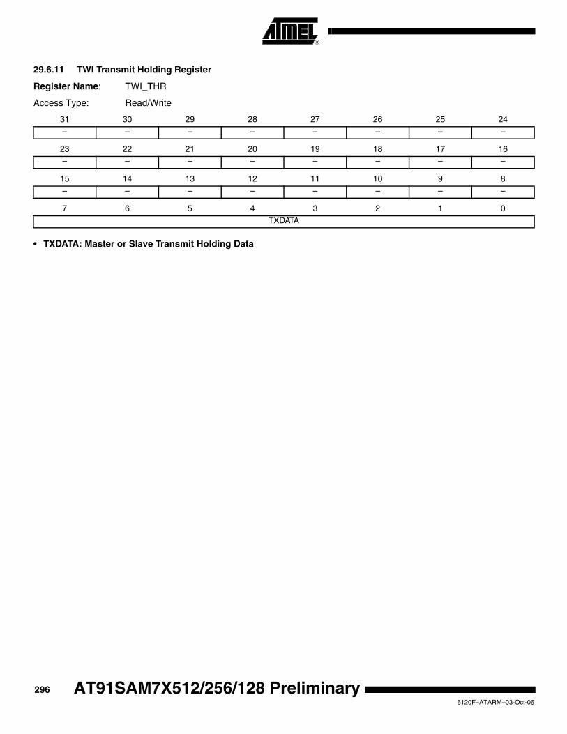
29.6.11 TWI Transmit Holding Register
Register Name: TWI_THR
Access Type: Read/Write
• TXDATA: Master or Slave Transmit Holding Data
31 30 29 28 27 26 25 24– – – – – – – –
23 22 21 20 19 18 17 16
– – – – – – – –
15 14 13 12 11 10 9 8– – – – – – – –
7 6 5 4 3 2 1 0
TXDATA
2966120F–ATARM–03-Oct-06
AT91SAM7X512/256/128 Preliminary

AT91SAM7X512/256/128 Preliminary
30. Universal Synchronous Asynchronous Receiver Transceiver (USART)
30.1 Overview
The Universal Synchronous Asynchronous Receiver Transceiver (USART) provides one full duplex universal synchronous asynchronous serial link. Data frame format is widely programma-ble (data length, parity, number of stop bits) to support a maximum of standards. The receiver implements parity error, framing error and overrun error detection. The receiver time-out enables handling variable-length frames and the transmitter timeguard facilitates communications with slow remote devices. Multidrop communications are also supported through address bit han-dling in reception and transmission.
The USART features three test modes: remote loopback, local loopback and automatic echo.
The USART supports specific operating modes providing interfaces on RS485 buses, with ISO7816 T = 0 or T = 1 smart card slots, infrared transceivers and connection to modem ports. The hardware handshaking feature enables an out-of-band flow control by automatic manage-ment of the pins RTS and CTS.
The USART supports the connection to the Peripheral DMA Controller, which enables data transfers to the transmitter and from the receiver. The PDC provides chained buffer manage-ment without any intervention of the processor.
2976120F–ATARM–03-Oct-06

30.2 Block Diagram
Figure 30-1. USART Block Diagram
Peripheral DMAController
Channel Channel
AIC
Receiver
USART Interrupt
RXD
TXD
SCK
USART PIOController
CTS
RTS
DTR
DSR
DCD
RI
Transmitter
Modem Signals Control
Baud Rate Generator
User Interface
PMCMCK
SLCK
DIVMCK/DIV
APB
2986120F–ATARM–03-Oct-06
AT91SAM7X512/256/128 Preliminary
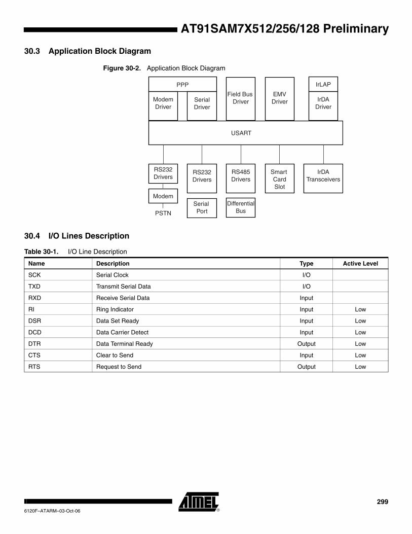
AT91SAM7X512/256/128 Preliminary
30.3 Application Block Diagram
Figure 30-2. Application Block Diagram
30.4 I/O Lines Description
Smart CardSlot
USART
RS232Drivers
Modem
RS485Drivers
DifferentialBus
IrDATransceivers
ModemDriver
Field Bus Driver
EMVDriver IrDA
Driver
IrLAP
RS232Drivers
Serial Port
SerialDriver
PPP
PSTN
Table 30-1. I/O Line Description
Name Description Type Active Level
SCK Serial Clock I/O
TXD Transmit Serial Data I/O
RXD Receive Serial Data Input
RI Ring Indicator Input Low
DSR Data Set Ready Input Low
DCD Data Carrier Detect Input Low
DTR Data Terminal Ready Output Low
CTS Clear to Send Input Low
RTS Request to Send Output Low
2996120F–ATARM–03-Oct-06

30.5 Product Dependencies
30.5.1 I/O Lines
The pins used for interfacing the USART may be multiplexed with the PIO lines. The program-mer must first program the PIO controller to assign the desired USART pins to their peripheral function. If I/O lines of the USART are not used by the application, they can be used for other purposes by the PIO Controller.
To prevent the TXD line from falling when the USART is disabled, the use of an internal pull up is mandatory.
All the pins of the modems may or may not be implemented on the USART within a product. Fre-quently, only the USART1 is fully equipped with all the modem signals. For the other USARTs of the product not equipped with the corresponding pin, the associated control bits and statuses have no effect on the behavior of the USART.
30.5.2 Power Management
The USART is not continuously clocked. The programmer must first enable the USART Clock in the Power Management Controller (PMC) before using the USART. However, if the application does not require USART operations, the USART clock can be stopped when not needed and be restarted later. In this case, the USART will resume its operations where it left off.
Configuring the USART does not require the USART clock to be enabled.
30.5.3 Interrupt
The USART interrupt line is connected on one of the internal sources of the Advanced Interrupt Controller. Using the USART interrupt requires the AIC to be programmed first. Note that it is not recommended to use the USART interrupt line in edge sensitive mode.
3006120F–ATARM–03-Oct-06
AT91SAM7X512/256/128 Preliminary
AT91SAM7X512/256/128 Preliminary
30.6 Functional Description
The USART is capable of managing several types of serial synchronous or asynchronous communications.
It supports the following communication modes:
• 5- to 9-bit full-duplex asynchronous serial communication
– MSB- or LSB-first
– 1, 1.5 or 2 stop bits
– Parity even, odd, marked, space or none
– By 8 or by 16 over-sampling receiver frequency
– Optional hardware handshaking
– Optional modem signals management
– Optional break management
– Optional multidrop serial communication
• High-speed 5- to 9-bit full-duplex synchronous serial communication
– MSB- or LSB-first
– 1 or 2 stop bits
– Parity even, odd, marked, space or none
– By 8 or by 16 over-sampling frequency
– Optional hardware handshaking
– Optional modem signals management
– Optional break management
– Optional multidrop serial communication
• RS485 with driver control signal
• ISO7816, T0 or T1 protocols for interfacing with smart cards
– NACK handling, error counter with repetition and iteration limit
• InfraRed IrDA Modulation and Demodulation
• Test modes
– Remote loopback, local loopback, automatic echo
30.6.1 Baud Rate Generator
The Baud Rate Generator provides the bit period clock named the Baud Rate Clock to both the receiver and the transmitter.
The Baud Rate Generator clock source can be selected by setting the USCLKS field in the Mode Register (US_MR) between:
• the Master Clock MCK
• a division of the Master Clock, the divider being product dependent, but generally set to 8
• the external clock, available on the SCK pin
The Baud Rate Generator is based upon a 16-bit divider, which is programmed with the CD field of the Baud Rate Generator Register (US_BRGR). If CD is programmed at 0, the Baud Rate Generator does not generate any clock. If CD is programmed at 1, the divider is bypassed and becomes inactive.
3016120F–ATARM–03-Oct-06
If the external SCK clock is selected, the duration of the low and high levels of the signal pro-vided on the SCK pin must be longer than a Master Clock (MCK) period. The frequency of the signal provided on SCK must be at least 4.5 times lower than MCK.
Figure 30-3. Baud Rate Generator
30.6.1.1 Baud Rate in Asynchronous Mode
If the USART is programmed to operate in asynchronous mode, the selected clock is first divided by CD, which is field programmed in the Baud Rate Generator Register (US_BRGR). The resulting clock is provided to the receiver as a sampling clock and then divided by 16 or 8, depending on the programming of the OVER bit in US_MR.
If OVER is set to 1, the receiver sampling is 8 times higher than the baud rate clock. If OVER is cleared, the sampling is performed at 16 times the baud rate clock.
The following formula performs the calculation of the Baud Rate.
This gives a maximum baud rate of MCK divided by 8, assuming that MCK is the highest possi-ble clock and that OVER is programmed at 1.
30.6.1.2 Baud Rate Calculation Example
Table 30-2 shows calculations of CD to obtain a baud rate at 38400 bauds for different source clock frequencies. This table also shows the actual resulting baud rate and the error.
MCK/DIV16-bit Counter
0
Baud Rate Clock
CD
CD
SamplingDivider
0
1
>1
Sampling Clock
Reserved
MCK
SCK
USCLKS
OVER
SCK
SYNC
SYNC
USCLKS = 3
1
0
2
30
1
0
1
FIDI
Baudrate SelectedClock8 2 Over–( )CD( )
--------------------------------------------=
Table 30-2. Baud Rate Example (OVER = 0)
Source ClockExpected Baud
Rate Calculation Result CD Actual Baud Rate Error
MHz Bit/s Bit/s
3 686 400 38 400 6.00 6 38 400.00 0.00%
4 915 200 38 400 8.00 8 38 400.00 0.00%
5 000 000 38 400 8.14 8 39 062.50 1.70%
7 372 800 38 400 12.00 12 38 400.00 0.00%
3026120F–ATARM–03-Oct-06
AT91SAM7X512/256/128 Preliminary

AT91SAM7X512/256/128 Preliminary
The baud rate is calculated with the following formula:
The baud rate error is calculated with the following formula. It is not recommended to work with an error higher than 5%.
30.6.1.3 Fractional Baud Rate in Asynchronous Mode
The Baud Rate generator previously defined is subject to the following limitation: the output fre-quency changes by only integer multiples of the reference frequency. An approach to this problem is to integrate a fractional N clock generator that has a high resolution. The generator architecture is modified to obtain Baud Rate changes by a fraction of the reference source clock. This fractional part is programmed with the FP field in the Baud Rate Generator Register (US_BRGR). If FP is not 0, the fractional part is activated. The resolution is one eighth of the clock divider. This feature is only available when using USART normal mode. The fractional Baud Rate is calculated using the following formula:
The modified architecture is presented below:
8 000 000 38 400 13.02 13 38 461.54 0.16%
12 000 000 38 400 19.53 20 37 500.00 2.40%
12 288 000 38 400 20.00 20 38 400.00 0.00%
14 318 180 38 400 23.30 23 38 908.10 1.31%
14 745 600 38 400 24.00 24 38 400.00 0.00%
18 432 000 38 400 30.00 30 38 400.00 0.00%
24 000 000 38 400 39.06 39 38 461.54 0.16%
24 576 000 38 400 40.00 40 38 400.00 0.00%
25 000 000 38 400 40.69 40 38 109.76 0.76%
32 000 000 38 400 52.08 52 38 461.54 0.16%
32 768 000 38 400 53.33 53 38 641.51 0.63%
33 000 000 38 400 53.71 54 38 194.44 0.54%
40 000 000 38 400 65.10 65 38 461.54 0.16%
50 000 000 38 400 81.38 81 38 580.25 0.47%
Table 30-2. Baud Rate Example (OVER = 0) (Continued)
Source ClockExpected Baud
Rate Calculation Result CD Actual Baud Rate Error
BaudRate MCK CD 16×⁄=
Error 1 ExpectedBaudRateActualBaudRate
---------------------------------------------------⎝ ⎠⎛ ⎞–=
Baudrate SelectedClock
8 2 Over–( ) CD FP8
-------+⎝ ⎠⎛ ⎞
⎝ ⎠⎛ ⎞-----------------------------------------------------------------=
3036120F–ATARM–03-Oct-06
Figure 30-4. Fractional Baud Rate Generator
30.6.1.4 Baud Rate in Synchronous Mode
If the USART is programmed to operate in synchronous mode, the selected clock is simply divided by the field CD in US_BRGR.
In synchronous mode, if the external clock is selected (USCLKS = 3), the clock is provided directly by the signal on the USART SCK pin. No division is active. The value written in US_BRGR has no effect. The external clock frequency must be at least 4.5 times lower than the system clock.
When either the external clock SCK or the internal clock divided (MCK/DIV) is selected, the value programmed in CD must be even if the user has to ensure a 50:50 mark/space ratio on the SCK pin. If the internal clock MCK is selected, the Baud Rate Generator ensures a 50:50 duty cycle on the SCK pin, even if the value programmed in CD is odd.
30.6.1.5 Baud Rate in ISO 7816 Mode
The ISO7816 specification defines the bit rate with the following formula:
where:
• B is the bit rate
• Di is the bit-rate adjustment factor
• Fi is the clock frequency division factor
• f is the ISO7816 clock frequency (Hz)
MCK/DIV16-bit Counter
0
Baud Rate Clock
CD
CD
SamplingDivider
0
1
>1
Sampling Clock
Reserved
MCK
SCK
USCLKS
OVER
SCK
SYNC
SYNC
USCLKS = 3
1
0
2
30
1
0
1
FIDIglitch-free logic
Modulus Control
FP
FP
BaudRate SelectedClockCD
--------------------------------------=
B DiFi------ f×=
3046120F–ATARM–03-Oct-06
AT91SAM7X512/256/128 Preliminary

AT91SAM7X512/256/128 Preliminary
Di is a binary value encoded on a 4-bit field, named DI, as represented in Table 30-3.
Fi is a binary value encoded on a 4-bit field, named FI, as represented in Table 30-4.
Table 30-5 shows the resulting Fi/Di Ratio, which is the ratio between the ISO7816 clock and the baud rate clock.
If the USART is configured in ISO7816 Mode, the clock selected by the USCLKS field in the Mode Register (US_MR) is first divided by the value programmed in the field CD in the Baud Rate Generator Register (US_BRGR). The resulting clock can be provided to the SCK pin to feed the smart card clock inputs. This means that the CLKO bit can be set in US_MR.
This clock is then divided by the value programmed in the FI_DI_RATIO field in the FI_DI_Ratio register (US_FIDI). This is performed by the Sampling Divider, which performs a division by up to 2047 in ISO7816 Mode. The non-integer values of the Fi/Di Ratio are not supported and the user must program the FI_DI_RATIO field to a value as close as possible to the expected value.
The FI_DI_RATIO field resets to the value 0x174 (372 in decimal) and is the most common divider between the ISO7816 clock and the bit rate (Fi = 372, Di = 1).
Figure 30-5 shows the relation between the Elementary Time Unit, corresponding to a bit time, and the ISO 7816 clock.
Table 30-3. Binary and Decimal Values for Di
DI field 0001 0010 0011 0100 0101 0110 1000 1001
Di (decimal) 1 2 4 8 16 32 12 20
Table 30-4. Binary and Decimal Values for Fi
FI field 0000 0001 0010 0011 0100 0101 0110 1001 1010 1011 1100 1101
Fi (decimal 372 372 558 744 1116 1488 1860 512 768 1024 1536 2048
Table 30-5. Possible Values for the Fi/Di Ratio
Fi/Di 372 558 774 1116 1488 1806 512 768 1024 1536 2048
1 372 558 744 1116 1488 1860 512 768 1024 1536 2048
2 186 279 372 558 744 930 256 384 512 768 1024
4 93 139.5 186 279 372 465 128 192 256 384 512
8 46.5 69.75 93 139.5 186 232.5 64 96 128 192 256
16 23.25 34.87 46.5 69.75 93 116.2 32 48 64 96 128
32 11.62 17.43 23.25 34.87 46.5 58.13 16 24 32 48 64
12 31 46.5 62 93 124 155 42.66 64 85.33 128 170.6
20 18.6 27.9 37.2 55.8 74.4 93 25.6 38.4 51.2 76.8 102.4
3056120F–ATARM–03-Oct-06
Figure 30-5. Elementary Time Unit (ETU)
30.6.2 Receiver and Transmitter Control
After reset, the receiver is disabled. The user must enable the receiver by setting the RXEN bit in the Control Register (US_CR). However, the receiver registers can be programmed before the receiver clock is enabled.
After reset, the transmitter is disabled. The user must enable it by setting the TXEN bit in the Control Register (US_CR). However, the transmitter registers can be programmed before being enabled.
The Receiver and the Transmitter can be enabled together or independently.
At any time, the software can perform a reset on the receiver or the transmitter of the USART by setting the corresponding bit, RSTRX and RSTTX respectively, in the Control Register (US_CR). The reset commands have the same effect as a hardware reset on the corresponding logic. Regardless of what the receiver or the transmitter is performing, the communication is immediately stopped.
The user can also independently disable the receiver or the transmitter by setting RXDIS and TXDIS respectively in US_CR. If the receiver is disabled during a character reception, the USART waits until the end of reception of the current character, then the reception is stopped. If the transmitter is disabled while it is operating, the USART waits the end of transmission of both the current character and character being stored in the Transmit Holding Register (US_THR). If a timeguard is programmed, it is handled normally.
30.6.3 Synchronous and Asynchronous Modes
30.6.3.1 Transmitter Operations
The transmitter performs the same in both synchronous and asynchronous operating modes (SYNC = 0 or SYNC = 1). One start bit, up to 9 data bits, one optional parity bit and up to two stop bits are successively shifted out on the TXD pin at each falling edge of the programmed serial clock.
The number of data bits is selected by the CHRL field and the MODE 9 bit in the Mode Register (US_MR). Nine bits are selected by setting the MODE 9 bit regardless of the CHRL field. The parity bit is set according to the PAR field in US_MR. The even, odd, space, marked or none parity bit can be configured. The MSBF field in US_MR configures which data bit is sent first. If written at 1, the most significant bit is sent first. At 0, the less significant bit is sent first. The num-ber of stop bits is selected by the NBSTOP field in US_MR. The 1.5 stop bit is supported in asynchronous mode only.
1 ETU
ISO7816 Clockon SCK
ISO7816 I/O Lineon TXD
FI_DI_RATIOISO7816 Clock Cycles
3066120F–ATARM–03-Oct-06
AT91SAM7X512/256/128 Preliminary

AT91SAM7X512/256/128 Preliminary
Figure 30-6. Character Transmit
The characters are sent by writing in the Transmit Holding Register (US_THR). The transmitter reports two status bits in the Channel Status Register (US_CSR): TXRDY (Transmitter Ready), which indicates that US_THR is empty and TXEMPTY, which indicates that all the characters written in US_THR have been processed. When the current character processing is completed, the last character written in US_THR is transferred into the Shift Register of the transmitter and US_THR becomes empty, thus TXRDY raises.
Both TXRDY and TXEMPTY bits are low since the transmitter is disabled. Writing a character in US_THR while TXRDY is active has no effect and the written character is lost.
Figure 30-7. Transmitter Status
30.6.3.2 Asynchronous Receiver
If the USART is programmed in asynchronous operating mode (SYNC = 0), the receiver over-samples the RXD input line. The oversampling is either 16 or 8 times the Baud Rate clock, depending on the OVER bit in the Mode Register (US_MR).
The receiver samples the RXD line. If the line is sampled during one half of a bit time at 0, a start bit is detected and data, parity and stop bits are successively sampled on the bit rate clock.
If the oversampling is 16, (OVER at 0), a start is detected at the eighth sample at 0. Then, data bits, parity bit and stop bit are sampled on each 16 sampling clock cycle. If the oversampling is 8 (OVER at 1), a start bit is detected at the fourth sample at 0. Then, data bits, parity bit and stop bit are sampled on each 8 sampling clock cycle.
The number of data bits, first bit sent and parity mode are selected by the same fields and bits as the transmitter, i.e. respectively CHRL, MODE9, MSBF and PAR. For the synchronization mechanism only, the number of stop bits has no effect on the receiver as it considers only one
D0 D1 D2 D3 D4 D5 D6 D7
TXD
Start Bit
ParityBit
StopBit
Example: 8-bit, Parity Enabled One Stop
Baud Rate Clock
D0 D1 D2 D3 D4 D5 D6 D7
TXD
Start Bit
ParityBit
StopBit
Baud Rate Clock
Start Bit
WriteUS_THR
D0 D1 D2 D3 D4 D5 D6 D7Parity
BitStopBit
TXRDY
TXEMPTY
3076120F–ATARM–03-Oct-06

stop bit, regardless of the field NBSTOP, so that resynchronization between the receiver and the transmitter can occur. Moreover, as soon as the stop bit is sampled, the receiver starts looking for a new start bit so that resynchronization can also be accomplished when the transmitter is operating with one stop bit.
Figure 30-8 and Figure 30-9 illustrate start detection and character reception when USART operates in asynchronous mode.
Figure 30-8. Asynchronous Start Detection
Figure 30-9. Asynchronous Character Reception
30.6.3.3 Synchronous Receiver
In synchronous mode (SYNC = 1), the receiver samples the RXD signal on each rising edge of the Baud Rate Clock. If a low level is detected, it is considered as a start. All data bits, the parity bit and the stop bits are sampled and the receiver waits for the next start bit. Synchronous mode operations provide a high speed transfer capability.
Configuration fields and bits are the same as in asynchronous mode.
Figure 30-10 illustrates a character reception in synchronous mode.
SamplingClock (x16)
RXD
Start Detection
Sampling
Baud RateClock
RXD
Start Rejection
Sampling
1 2 3 4 5 6 7 8
1 2 3 4 5 6 7 0 1 2 3 4
1 2 3 4 5 6 7 8 9 10 11 12 13 14 15 16D0
Sampling
D0 D1 D2 D3 D4 D5 D6 D7
RXD
ParityBit
StopBit
Example: 8-bit, Parity Enabled
Baud RateClock
Start Detection
16 samples
16 samples
16 samples
16 samples
16 samples
16 samples
16 samples
16 samples
16 samples
16 samples
3086120F–ATARM–03-Oct-06
AT91SAM7X512/256/128 Preliminary

AT91SAM7X512/256/128 Preliminary
Figure 30-10. Synchronous Mode Character Reception
30.6.3.4 Receiver Operations
When a character reception is completed, it is transferred to the Receive Holding Register (US_RHR) and the RXRDY bit in the Status Register (US_CSR) rises. If a character is com-pleted while the RXRDY is set, the OVRE (Overrun Error) bit is set. The last character is transferred into US_RHR and overwrites the previous one. The OVRE bit is cleared by writing the Control Register (US_CR) with the RSTSTA (Reset Status) bit at 1.
Figure 30-11. Receiver Status
D0 D1 D2 D3 D4 D5 D6 D7
RXD
Start Sampling
Parity BitStop Bit
Example: 8-bit, Parity Enabled 1 Stop
Baud RateClock
D0 D1 D2 D3 D4 D5 D6 D7
RXD
Start Bit
ParityBit
StopBit
Baud Rate Clock
WriteUS_CR
RXRDY
OVRE
D0 D1 D2 D3 D4 D5 D6 D7Start
BitParity
BitStopBit
RSTSTA = 1
ReadUS_RHR
3096120F–ATARM–03-Oct-06
30.6.3.5 Parity
The USART supports five parity modes selected by programming the PAR field in the Mode Register (US_MR). The PAR field also enables the Multidrop mode, see ”Multidrop Mode” on page 311. Even and odd parity bit generation and error detection are supported.
If even parity is selected, the parity generator of the transmitter drives the parity bit at 0 if a num-ber of 1s in the character data bit is even, and at 1 if the number of 1s is odd. Accordingly, the receiver parity checker counts the number of received 1s and reports a parity error if the sam-pled parity bit does not correspond. If odd parity is selected, the parity generator of the transmitter drives the parity bit at 1 if a number of 1s in the character data bit is even, and at 0 if the number of 1s is odd. Accordingly, the receiver parity checker counts the number of received 1s and reports a parity error if the sampled parity bit does not correspond. If the mark parity is used, the parity generator of the transmitter drives the parity bit at 1 for all characters. The receiver parity checker reports an error if the parity bit is sampled at 0. If the space parity is used, the parity generator of the transmitter drives the parity bit at 0 for all characters. The receiver parity checker reports an error if the parity bit is sampled at 1. If parity is disabled, the transmitter does not generate any parity bit and the receiver does not report any parity error.
Table 30-6 shows an example of the parity bit for the character 0x41 (character ASCII “A”) depending on the configuration of the USART. Because there are two bits at 1, 1 bit is added when a parity is odd, or 0 is added when a parity is even.
When the receiver detects a parity error, it sets the PARE (Parity Error) bit in the Channel Status Register (US_CSR). The PARE bit can be cleared by writing the Control Register (US_CR) with the RSTSTA bit at 1. Figure 30-12 illustrates the parity bit status setting and clearing.
Table 30-6. Parity Bit Examples
Character Hexa Binary Parity Bit Parity Mode
A 0x41 0100 0001 1 Odd
A 0x41 0100 0001 0 Even
A 0x41 0100 0001 1 Mark
A 0x41 0100 0001 0 Space
A 0x41 0100 0001 None None
3106120F–ATARM–03-Oct-06
AT91SAM7X512/256/128 Preliminary

AT91SAM7X512/256/128 Preliminary
Figure 30-12. Parity Error
30.6.3.6 Multidrop Mode
If the PAR field in the Mode Register (US_MR) is programmed to the value 0x6 or 0x07, the USART runs in Multidrop Mode. This mode differentiates the data characters and the address characters. Data is transmitted with the parity bit at 0 and addresses are transmitted with the parity bit at 1.
If the USART is configured in multidrop mode, the receiver sets the PARE parity error bit when the parity bit is high and the transmitter is able to send a character with the parity bit high when the Control Register is written with the SENDA bit at 1.
To handle parity error, the PARE bit is cleared when the Control Register is written with the bit RSTSTA at 1.
The transmitter sends an address byte (parity bit set) when SENDA is written to US_CR. In this case, the next byte written to US_THR is transmitted as an address. Any character written in US_THR without having written the command SENDA is transmitted normally with the parity at 0.
30.6.3.7 Transmitter Timeguard
The timeguard feature enables the USART interface with slow remote devices.
The timeguard function enables the transmitter to insert an idle state on the TXD line between two characters. This idle state actually acts as a long stop bit.
The duration of the idle state is programmed in the TG field of the Transmitter Timeguard Regis-ter (US_TTGR). When this field is programmed at zero no timeguard is generated. Otherwise, the transmitter holds a high level on TXD after each transmitted byte during the number of bit periods programmed in TG in addition to the number of stop bits.
As illustrated in Figure 30-13, the behavior of TXRDY and TXEMPTY status bits is modified by the programming of a timeguard. TXRDY rises only when the start bit of the next character is sent, and thus remains at 0 during the timeguard transmission if a character has been written in US_THR. TXEMPTY remains low until the timeguard transmission is completed as the time-guard is part of the current character being transmitted.
D0 D1 D2 D3 D4 D5 D6 D7
RXD
Start Bit
BadParity
Bit
StopBit
Baud Rate Clock
WriteUS_CR
PARE
RXRDY
RSTSTA = 1
3116120F–ATARM–03-Oct-06
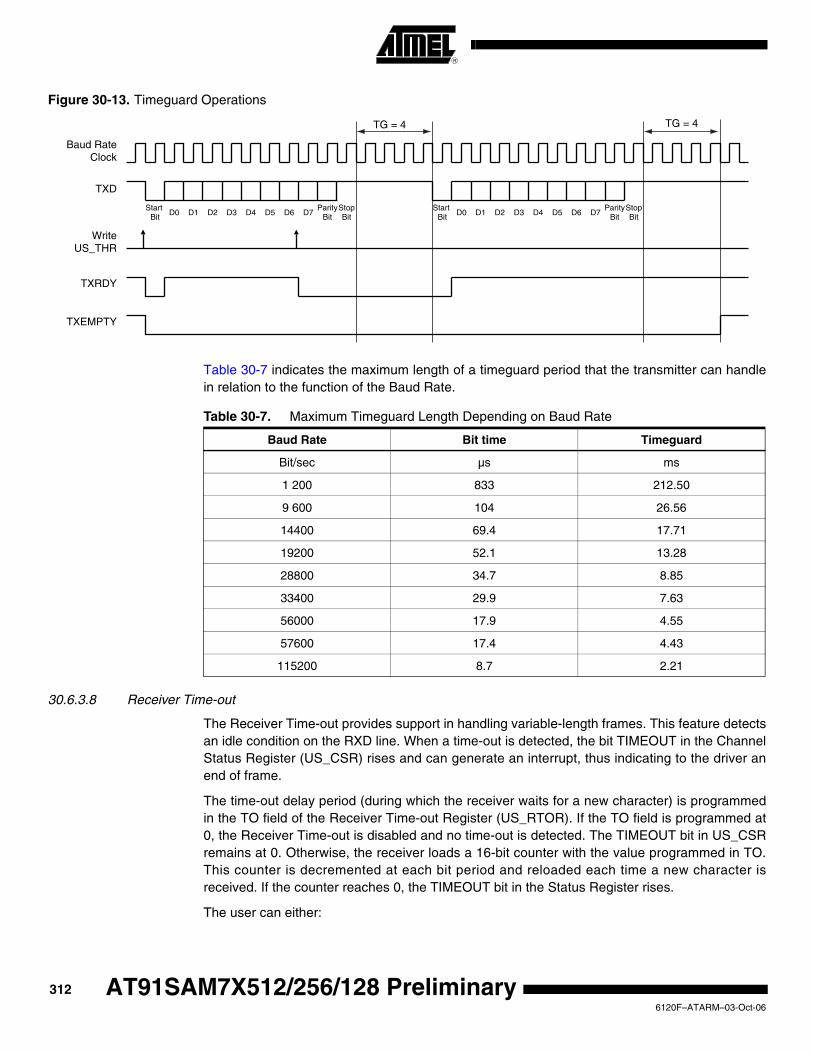
Figure 30-13. Timeguard Operations
Table 30-7 indicates the maximum length of a timeguard period that the transmitter can handle in relation to the function of the Baud Rate.
30.6.3.8 Receiver Time-out
The Receiver Time-out provides support in handling variable-length frames. This feature detects an idle condition on the RXD line. When a time-out is detected, the bit TIMEOUT in the Channel Status Register (US_CSR) rises and can generate an interrupt, thus indicating to the driver an end of frame.
The time-out delay period (during which the receiver waits for a new character) is programmed in the TO field of the Receiver Time-out Register (US_RTOR). If the TO field is programmed at 0, the Receiver Time-out is disabled and no time-out is detected. The TIMEOUT bit in US_CSR remains at 0. Otherwise, the receiver loads a 16-bit counter with the value programmed in TO. This counter is decremented at each bit period and reloaded each time a new character is received. If the counter reaches 0, the TIMEOUT bit in the Status Register rises.
The user can either:
D0 D1 D2 D3 D4 D5 D6 D7
TXD
Start Bit
ParityBit
StopBit
Baud Rate Clock
Start Bit
TG = 4
WriteUS_THR
D0 D1 D2 D3 D4 D5 D6 D7Parity
BitStopBit
TXRDY
TXEMPTY
TG = 4
Table 30-7. Maximum Timeguard Length Depending on Baud Rate
Baud Rate Bit time Timeguard
Bit/sec µs ms
1 200 833 212.50
9 600 104 26.56
14400 69.4 17.71
19200 52.1 13.28
28800 34.7 8.85
33400 29.9 7.63
56000 17.9 4.55
57600 17.4 4.43
115200 8.7 2.21
3126120F–ATARM–03-Oct-06
AT91SAM7X512/256/128 Preliminary

AT91SAM7X512/256/128 Preliminary
• Stop the counter clock until a new character is received. This is performed by writing the Control Register (US_CR) with the STTTO (Start Time-out) bit at 1. In this case, the idle state on RXD before a new character is received will not provide a time-out. This prevents having to handle an interrupt before a character is received and allows waiting for the next idle state on RXD after a frame is received.
• Obtain an interrupt while no character is received. This is performed by writing US_CR with the RETTO (Reload and Start Time-out) bit at 1. If RETTO is performed, the counter starts counting down immediately from the value TO. This enables generation of a periodic interrupt so that a user time-out can be handled, for example when no key is pressed on a keyboard.
If STTTO is performed, the counter clock is stopped until a first character is received. The idle state on RXD before the start of the frame does not provide a time-out. This prevents having to obtain a periodic interrupt and enables a wait of the end of frame when the idle state on RXD is detected.
If RETTO is performed, the counter starts counting down immediately from the value TO. This enables generation of a periodic interrupt so that a user time-out can be handled, for example when no key is pressed on a keyboard.
Figure 30-14 shows the block diagram of the Receiver Time-out feature.
Figure 30-14. Receiver Time-out Block Diagram
Table 30-8 gives the maximum time-out period for some standard baud rates.
Table 30-8. Maximum Time-out Period
Baud Rate Bit Time Time-out
bit/sec µs ms
600 1 667 109 225
1 200 833 54 613
2 400 417 27 306
4 800 208 13 653
9 600 104 6 827
14400 69 4 551
19200 52 3 413
28800 35 2 276
33400 30 1 962
16-bit Time-out Counter
0
TO
TIMEOUT
Baud Rate Clock
=
CharacterReceived
RETTO
Load
Clock
16-bit Value
STTTO
D Q1
Clear
3136120F–ATARM–03-Oct-06

30.6.3.9 Framing Error
The receiver is capable of detecting framing errors. A framing error happens when the stop bit of a received character is detected at level 0. This can occur if the receiver and the transmitter are fully desynchronized.
A framing error is reported on the FRAME bit of the Channel Status Register (US_CSR). The FRAME bit is asserted in the middle of the stop bit as soon as the framing error is detected. It is cleared by writing the Control Register (US_CR) with the RSTSTA bit at 1.
Figure 30-15. Framing Error Status
30.6.3.10 Transmit Break
The user can request the transmitter to generate a break condition on the TXD line. A break con-dition drives the TXD line low during at least one complete character. It appears the same as a 0x00 character sent with the parity and the stop bits at 0. However, the transmitter holds the TXD line at least during one character until the user requests the break condition to be removed.
A break is transmitted by writing the Control Register (US_CR) with the STTBRK bit at 1. This can be performed at any time, either while the transmitter is empty (no character in either the Shift Register or in US_THR) or when a character is being transmitted. If a break is requested while a character is being shifted out, the character is first completed before the TXD line is held low.
Once STTBRK command is requested further STTBRK commands are ignored until the end of the break is completed.
The break condition is removed by writing US_CR with the STPBRK bit at 1. If the STPBRK is requested before the end of the minimum break duration (one character, including start, data, parity and stop bits), the transmitter ensures that the break condition completes.
56000 18 1 170
57600 17 1 138
200000 5 328
Table 30-8. Maximum Time-out Period (Continued)
Baud Rate Bit Time Time-out
D0 D1 D2 D3 D4 D5 D6 D7
RXD
Start Bit
ParityBit
StopBit
Baud Rate Clock
WriteUS_CR
FRAME
RXRDY
RSTSTA = 1
3146120F–ATARM–03-Oct-06
AT91SAM7X512/256/128 Preliminary
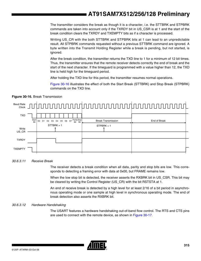
AT91SAM7X512/256/128 Preliminary
The transmitter considers the break as though it is a character, i.e. the STTBRK and STPBRK commands are taken into account only if the TXRDY bit in US_CSR is at 1 and the start of the break condition clears the TXRDY and TXEMPTY bits as if a character is processed.
Writing US_CR with the both STTBRK and STPBRK bits at 1 can lead to an unpredictable result. All STPBRK commands requested without a previous STTBRK command are ignored. A byte written into the Transmit Holding Register while a break is pending, but not started, is ignored.
After the break condition, the transmitter returns the TXD line to 1 for a minimum of 12 bit times. Thus, the transmitter ensures that the remote receiver detects correctly the end of break and the start of the next character. If the timeguard is programmed with a value higher than 12, the TXD line is held high for the timeguard period.
After holding the TXD line for this period, the transmitter resumes normal operations.
Figure 30-16 illustrates the effect of both the Start Break (STTBRK) and Stop Break (STPBRK) commands on the TXD line.
Figure 30-16. Break Transmission
30.6.3.11 Receive Break
The receiver detects a break condition when all data, parity and stop bits are low. This corre-sponds to detecting a framing error with data at 0x00, but FRAME remains low.
When the low stop bit is detected, the receiver asserts the RXBRK bit in US_CSR. This bit may be cleared by writing the Control Register (US_CR) with the bit RSTSTA at 1.
An end of receive break is detected by a high level for at least 2/16 of a bit period in asynchro-nous operating mode or one sample at high level in synchronous operating mode. The end of break detection also asserts the RXBRK bit.
30.6.3.12 Hardware Handshaking
The USART features a hardware handshaking out-of-band flow control. The RTS and CTS pins are used to connect with the remote device, as shown in Figure 30-17.
D0 D1 D2 D3 D4 D5 D6 D7
TXD
Start Bit
ParityBit
StopBit
Baud Rate Clock
WriteUS_CR
TXRDY
TXEMPTY
STPBRK = 1STTBRK = 1
Break Transmission End of Break
3156120F–ATARM–03-Oct-06
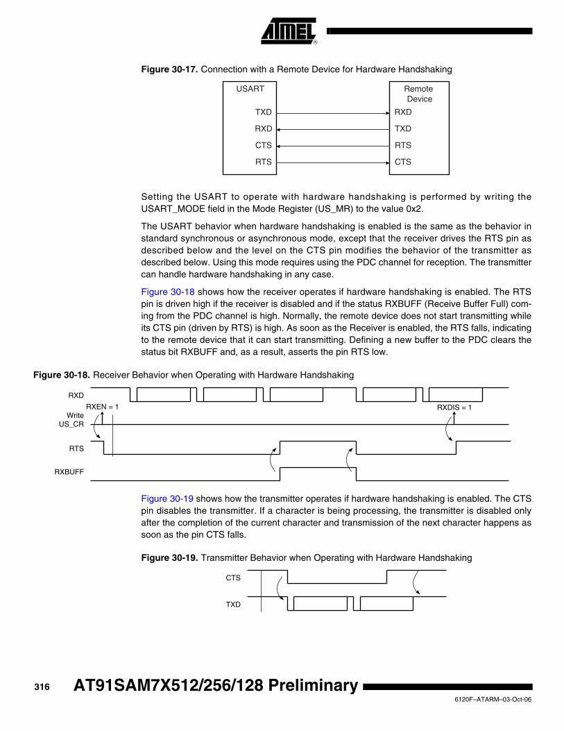
Figure 30-17. Connection with a Remote Device for Hardware Handshaking
Setting the USART to operate with hardware handshaking is performed by writing the USART_MODE field in the Mode Register (US_MR) to the value 0x2.
The USART behavior when hardware handshaking is enabled is the same as the behavior in standard synchronous or asynchronous mode, except that the receiver drives the RTS pin as described below and the level on the CTS pin modifies the behavior of the transmitter as described below. Using this mode requires using the PDC channel for reception. The transmitter can handle hardware handshaking in any case.
Figure 30-18 shows how the receiver operates if hardware handshaking is enabled. The RTS pin is driven high if the receiver is disabled and if the status RXBUFF (Receive Buffer Full) com-ing from the PDC channel is high. Normally, the remote device does not start transmitting while its CTS pin (driven by RTS) is high. As soon as the Receiver is enabled, the RTS falls, indicating to the remote device that it can start transmitting. Defining a new buffer to the PDC clears the status bit RXBUFF and, as a result, asserts the pin RTS low.
Figure 30-18. Receiver Behavior when Operating with Hardware Handshaking
Figure 30-19 shows how the transmitter operates if hardware handshaking is enabled. The CTS pin disables the transmitter. If a character is being processing, the transmitter is disabled only after the completion of the current character and transmission of the next character happens as soon as the pin CTS falls.
Figure 30-19. Transmitter Behavior when Operating with Hardware Handshaking
USART
TXD
CTS
Remote Device
RXD
TXDRXD
RTS
RTS
CTS
RTS
RXBUFF
WriteUS_CR
RXEN = 1
RXD
RXDIS = 1
CTS
TXD
3166120F–ATARM–03-Oct-06
AT91SAM7X512/256/128 Preliminary
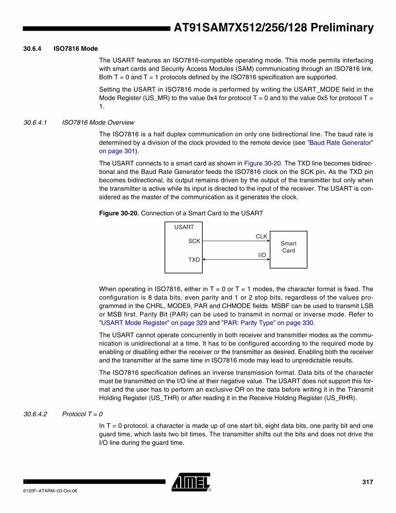
AT91SAM7X512/256/128 Preliminary
30.6.4 ISO7816 Mode
The USART features an ISO7816-compatible operating mode. This mode permits interfacing with smart cards and Security Access Modules (SAM) communicating through an ISO7816 link. Both T = 0 and T = 1 protocols defined by the ISO7816 specification are supported.
Setting the USART in ISO7816 mode is performed by writing the USART_MODE field in the Mode Register (US_MR) to the value 0x4 for protocol T = 0 and to the value 0x5 for protocol T = 1.
30.6.4.1 ISO7816 Mode Overview
The ISO7816 is a half duplex communication on only one bidirectional line. The baud rate is determined by a division of the clock provided to the remote device (see ”Baud Rate Generator” on page 301).
The USART connects to a smart card as shown in Figure 30-20. The TXD line becomes bidirec-tional and the Baud Rate Generator feeds the ISO7816 clock on the SCK pin. As the TXD pin becomes bidirectional, its output remains driven by the output of the transmitter but only when the transmitter is active while its input is directed to the input of the receiver. The USART is con-sidered as the master of the communication as it generates the clock.
Figure 30-20. Connection of a Smart Card to the USART
When operating in ISO7816, either in T = 0 or T = 1 modes, the character format is fixed. The configuration is 8 data bits, even parity and 1 or 2 stop bits, regardless of the values pro-grammed in the CHRL, MODE9, PAR and CHMODE fields. MSBF can be used to transmit LSB or MSB first. Parity Bit (PAR) can be used to transmit in normal or inverse mode. Refer to ”USART Mode Register” on page 329 and ”PAR: Parity Type” on page 330.
The USART cannot operate concurrently in both receiver and transmitter modes as the commu-nication is unidirectional at a time. It has to be configured according to the required mode by enabling or disabling either the receiver or the transmitter as desired. Enabling both the receiver and the transmitter at the same time in ISO7816 mode may lead to unpredictable results.
The ISO7816 specification defines an inverse transmission format. Data bits of the character must be transmitted on the I/O line at their negative value. The USART does not support this for-mat and the user has to perform an exclusive OR on the data before writing it in the Transmit Holding Register (US_THR) or after reading it in the Receive Holding Register (US_RHR).
30.6.4.2 Protocol T = 0
In T = 0 protocol, a character is made up of one start bit, eight data bits, one parity bit and one guard time, which lasts two bit times. The transmitter shifts out the bits and does not drive the I/O line during the guard time.
SmartCard
SCKCLK
TXDI/O
USART
3176120F–ATARM–03-Oct-06
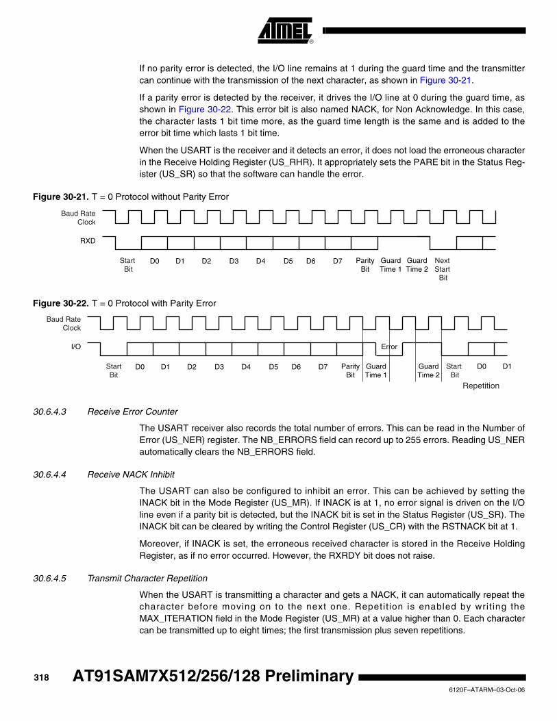
If no parity error is detected, the I/O line remains at 1 during the guard time and the transmitter can continue with the transmission of the next character, as shown in Figure 30-21.
If a parity error is detected by the receiver, it drives the I/O line at 0 during the guard time, as shown in Figure 30-22. This error bit is also named NACK, for Non Acknowledge. In this case, the character lasts 1 bit time more, as the guard time length is the same and is added to the error bit time which lasts 1 bit time.
When the USART is the receiver and it detects an error, it does not load the erroneous character in the Receive Holding Register (US_RHR). It appropriately sets the PARE bit in the Status Reg-ister (US_SR) so that the software can handle the error.
Figure 30-21. T = 0 Protocol without Parity Error
Figure 30-22. T = 0 Protocol with Parity Error
30.6.4.3 Receive Error Counter
The USART receiver also records the total number of errors. This can be read in the Number of Error (US_NER) register. The NB_ERRORS field can record up to 255 errors. Reading US_NER automatically clears the NB_ERRORS field.
30.6.4.4 Receive NACK Inhibit
The USART can also be configured to inhibit an error. This can be achieved by setting the INACK bit in the Mode Register (US_MR). If INACK is at 1, no error signal is driven on the I/O line even if a parity bit is detected, but the INACK bit is set in the Status Register (US_SR). The INACK bit can be cleared by writing the Control Register (US_CR) with the RSTNACK bit at 1.
Moreover, if INACK is set, the erroneous received character is stored in the Receive Holding Register, as if no error occurred. However, the RXRDY bit does not raise.
30.6.4.5 Transmit Character Repetition
When the USART is transmitting a character and gets a NACK, it can automatically repeat the character before moving on to the next one. Repetit ion is enabled by writ ing the MAX_ITERATION field in the Mode Register (US_MR) at a value higher than 0. Each character can be transmitted up to eight times; the first transmission plus seven repetitions.
D0 D1 D2 D3 D4 D5 D6 D7
RXD
ParityBit
Baud RateClock
Start Bit
GuardTime 1
Next Start
Bit
GuardTime 2
D0 D1 D2 D3 D4 D5 D6 D7
I/O
ParityBit
Baud RateClock
StartBit
GuardTime 1
Start Bit
GuardTime 2
D0 D1
Error
Repetition
3186120F–ATARM–03-Oct-06
AT91SAM7X512/256/128 Preliminary

AT91SAM7X512/256/128 Preliminary
If MAX_ITERATION does not equal zero, the USART repeats the character as many times as the value loaded in MAX_ITERATION.
When the USART repetition number reaches MAX_ITERATION, the ITERATION bit is set in the Channel Status Register (US_CSR). If the repetition of the character is acknowledged by the receiver, the repetitions are stopped and the iteration counter is cleared.
The ITERATION bit in US_CSR can be cleared by writing the Control Register with the RSIT bit at 1.
30.6.4.6 Disable Successive Receive NACK
The receiver can limit the number of successive NACKs sent back to the remote transmitter. This is programmed by setting the bit DSNACK in the Mode Register (US_MR). The maximum number of NACK transmitted is programmed in the MAX_ITERATION field. As soon as MAX_ITERATION is reached, the character is considered as correct, an acknowledge is sent on the line and the ITERATION bit in the Channel Status Register is set.
30.6.4.7 Protocol T = 1
When operating in ISO7816 protocol T = 1, the transmission is similar to an asynchronous for-mat with only one stop bit. The parity is generated when transmitting and checked when receiving. Parity error detection sets the PARE bit in the Channel Status Register (US_CSR).
30.6.5 IrDA Mode
The USART features an IrDA mode supplying half-duplex point-to-point wireless communica-tion. It embeds the modulator and demodulator which allows a glueless connection to the infrared transceivers, as shown in Figure 30-23. The modulator and demodulator are compliant with the IrDA specification version 1.1 and support data transfer speeds ranging from 2.4 Kb/s to 115.2 Kb/s.
The USART IrDA mode is enabled by setting the USART_MODE field in the Mode Register (US_MR) to the value 0x8. The IrDA Filter Register (US_IF) allows configuring the demodulator filter. The USART transmitter and receiver operate in a normal asynchronous mode and all parameters are accessible. Note that the modulator and the demodulator are activated.
Figure 30-23. Connection to IrDA Transceivers
The receiver and the transmitter must be enabled or disabled according to the direction of the transmission to be managed.
IrDA Transceivers
RXD RX
TXD
TX
USART
Demodulator
Modulator
Receiver
Transmitter
3196120F–ATARM–03-Oct-06

30.6.5.1 IrDA Modulation
For baud rates up to and including 115.2 Kbits/sec, the RZI modulation scheme is used. “0” is represented by a light pulse of 3/16th of a bit time. Some examples of signal pulse duration are shown in Table 30-9.
Figure 30-24 shows an example of character transmission.
Figure 30-24. IrDA Modulation
30.6.5.2 IrDA Baud Rate
Table 30-10 gives some examples of CD values, baud rate error and pulse duration. Note that the requirement on the maximum acceptable error of ±1.87% must be met.
Table 30-9. IrDA Pulse Duration
Baud Rate Pulse Duration (3/16)
2.4 Kb/s 78.13 µs
9.6 Kb/s 19.53 µs
19.2 Kb/s 9.77 µs
38.4 Kb/s 4.88 µs
57.6 Kb/s 3.26 µs
115.2 Kb/s 1.63 µs
Bit Period Bit Period316
StartBit
Data Bits StopBit
0 00 0 01 11 11Transmitter
Output
TXD
Table 30-10. IrDA Baud Rate Error
Peripheral Clock Baud Rate CD Baud Rate Error Pulse Time
3 686 400 115 200 2 0.00% 1.63
20 000 000 115 200 11 1.38% 1.63
32 768 000 115 200 18 1.25% 1.63
40 000 000 115 200 22 1.38% 1.63
3 686 400 57 600 4 0.00% 3.26
20 000 000 57 600 22 1.38% 3.26
32 768 000 57 600 36 1.25% 3.26
40 000 000 57 600 43 0.93% 3.26
3 686 400 38 400 6 0.00% 4.88
3206120F–ATARM–03-Oct-06
AT91SAM7X512/256/128 Preliminary
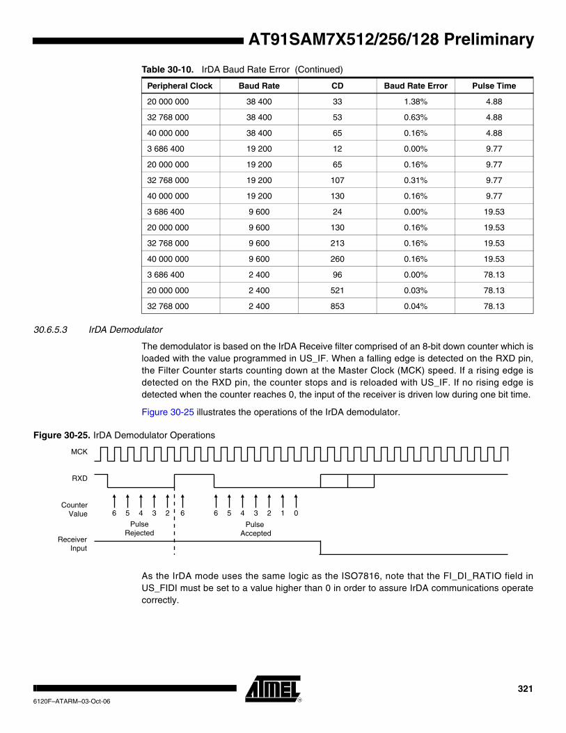
AT91SAM7X512/256/128 Preliminary
30.6.5.3 IrDA Demodulator
The demodulator is based on the IrDA Receive filter comprised of an 8-bit down counter which is loaded with the value programmed in US_IF. When a falling edge is detected on the RXD pin, the Filter Counter starts counting down at the Master Clock (MCK) speed. If a rising edge is detected on the RXD pin, the counter stops and is reloaded with US_IF. If no rising edge is detected when the counter reaches 0, the input of the receiver is driven low during one bit time.
Figure 30-25 illustrates the operations of the IrDA demodulator.
Figure 30-25. IrDA Demodulator Operations
As the IrDA mode uses the same logic as the ISO7816, note that the FI_DI_RATIO field in US_FIDI must be set to a value higher than 0 in order to assure IrDA communications operate correctly.
20 000 000 38 400 33 1.38% 4.88
32 768 000 38 400 53 0.63% 4.88
40 000 000 38 400 65 0.16% 4.88
3 686 400 19 200 12 0.00% 9.77
20 000 000 19 200 65 0.16% 9.77
32 768 000 19 200 107 0.31% 9.77
40 000 000 19 200 130 0.16% 9.77
3 686 400 9 600 24 0.00% 19.53
20 000 000 9 600 130 0.16% 19.53
32 768 000 9 600 213 0.16% 19.53
40 000 000 9 600 260 0.16% 19.53
3 686 400 2 400 96 0.00% 78.13
20 000 000 2 400 521 0.03% 78.13
32 768 000 2 400 853 0.04% 78.13
Table 30-10. IrDA Baud Rate Error (Continued)
Peripheral Clock Baud Rate CD Baud Rate Error Pulse Time
MCK
RXD
ReceiverInput
PulseRejected
6 5 4 3 2 6 16 5 4 3 2 0
Pulse Accepted
CounterValue
3216120F–ATARM–03-Oct-06

30.6.6 RS485 Mode
The USART features the RS485 mode to enable line driver control. While operating in RS485 mode, the USART behaves as though in asynchronous or synchronous mode and configuration of all the parameters is possible. The difference is that the RTS pin is driven high when the transmitter is operating. The behavior of the RTS pin is controlled by the TXEMPTY bit. A typical connection of the USART to a RS485 bus is shown in Figure 30-26.
Figure 30-26. Typical Connection to a RS485 Bus
The USART is set in RS485 mode by programming the USART_MODE field in the Mode Regis-ter (US_MR) to the value 0x1.
The RTS pin is at a level inverse to the TXEMPTY bit. Significantly, the RTS pin remains high when a timeguard is programmed so that the line can remain driven after the last character com-pletion. Figure 30-27 gives an example of the RTS waveform during a character transmission when the timeguard is enabled.
Figure 30-27. Example of RTS Drive with Timeguard
USART
RTS
TXD
RXD
Differential Bus
D0 D1 D2 D3 D4 D5 D6 D7
TXD
Start Bit
ParityBit
StopBit
Baud Rate Clock
TG = 4
WriteUS_THR
TXRDY
TXEMPTY
RTS
3226120F–ATARM–03-Oct-06
AT91SAM7X512/256/128 Preliminary
AT91SAM7X512/256/128 Preliminary
30.6.7 Modem Mode
The USART features modem mode, which enables control of the signals: DTR (Data Terminal Ready), DSR (Data Set Ready), RTS (Request to Send), CTS (Clear to Send), DCD (Data Car-rier Detect) and RI (Ring Indicator). While operating in modem mode, the USART behaves as a DTE (Data Terminal Equipment) as it drives DTR and RTS and can detect level change on DSR, DCD, CTS and RI.
Setting the USART in modem mode is performed by writing the USART_MODE field in the Mode Register (US_MR) to the value 0x3. While operating in modem mode the USART behaves as though in asynchronous mode and all the parameter configurations are available.
Table 30-11 gives the correspondence of the USART signals with modem connection standards.
The control of the DTR output pin is performed by writing the Control Register (US_CR) with the DTRDIS and DTREN bits respectively at 1. The disable command forces the corresponding pin to its inactive level, i.e. high. The enable command forces the corresponding pin to its active level, i.e. low. RTS output pin is automatically controlled in this mode
The level changes are detected on the RI, DSR, DCD and CTS pins. If an input change is detected, the RIIC, DSRIC, DCDIC and CTSIC bits in the Channel Status Register (US_CSR) are set respectively and can trigger an interrupt. The status is automatically cleared when US_CSR is read. Furthermore, the CTS automatically disables the transmitter when it is detected at its inactive state. If a character is being transmitted when the CTS rises, the charac-ter transmission is completed before the transmitter is actually disabled.
30.6.8 Test Modes
The USART can be programmed to operate in three different test modes. The internal loopback capability allows on-board diagnostics. In the loopback mode the USART interface pins are dis-connected or not and reconfigured for loopback internally or externally.
30.6.8.1 Normal Mode
Normal mode connects the RXD pin on the receiver input and the transmitter output on the TXD pin.
Table 30-11. Circuit References
USART Pin V24 CCITT Direction
TXD 2 103 From terminal to modem
RTS 4 105 From terminal to modem
DTR 20 108.2 From terminal to modem
RXD 3 104 From modem to terminal
CTS 5 106 From terminal to modem
DSR 6 107 From terminal to modem
DCD 8 109 From terminal to modem
RI 22 125 From terminal to modem
3236120F–ATARM–03-Oct-06

Figure 30-28. Normal Mode Configuration
30.6.8.2 Automatic Echo Mode
Automatic echo mode allows bit-by-bit retransmission. When a bit is received on the RXD pin, it is sent to the TXD pin, as shown in Figure 30-29. Programming the transmitter has no effect on the TXD pin. The RXD pin is still connected to the receiver input, thus the receiver remains active.
Figure 30-29. Automatic Echo Mode Configuration
30.6.8.3 Local Loopback Mode
Local loopback mode connects the output of the transmitter directly to the input of the receiver, as shown in Figure 30-30. The TXD and RXD pins are not used. The RXD pin has no effect on the receiver and the TXD pin is continuously driven high, as in idle state.
Figure 30-30. Local Loopback Mode Configuration
30.6.8.4 Remote Loopback Mode
Remote loopback mode directly connects the RXD pin to the TXD pin, as shown in Figure 30-31. The transmitter and the receiver are disabled and have no effect. This mode allows bit-by-bit retransmission.
Receiver
Transmitter
RXD
TXD
Receiver
Transmitter
RXD
TXD
Receiver
Transmitter
RXD
TXD1
3246120F–ATARM–03-Oct-06
AT91SAM7X512/256/128 Preliminary
AT91SAM7X512/256/128 Preliminary
Figure 30-31. Remote Loopback Mode Configuration
Receiver
Transmitter
RXD
TXD
1
3256120F–ATARM–03-Oct-06

30.7 USART User Interface
Table 30-12. USART Memory Map
Offset Register Name Access Reset State
0x0000 Control Register US_CR Write-only –
0x0004 Mode Register US_MR Read/Write –
0x0008 Interrupt Enable Register US_IER Write-only –
0x000C Interrupt Disable Register US_IDR Write-only –
0x0010 Interrupt Mask Register US_IMR Read-only 0x0
0x0014 Channel Status Register US_CSR Read-only –
0x0018 Receiver Holding Register US_RHR Read-only 0x0
0x001C Transmitter Holding Register US_THR Write-only –
0x0020 Baud Rate Generator Register US_BRGR Read/Write 0x0
0x0024 Receiver Time-out Register US_RTOR Read/Write 0x0
0x0028 Transmitter Timeguard Register US_TTGR Read/Write 0x0
0x2C - 0x3C Reserved – – –
0x0040 FI DI Ratio Register US_FIDI Read/Write 0x174
0x0044 Number of Errors Register US_NER Read-only –
0x0048 Reserved – – –
0x004C IrDA Filter Register US_IF Read/Write 0x0
0x5C - 0xFC Reserved – – –
0x100 - 0x128 Reserved for PDC Registers – – –
3266120F–ATARM–03-Oct-06
AT91SAM7X512/256/128 Preliminary
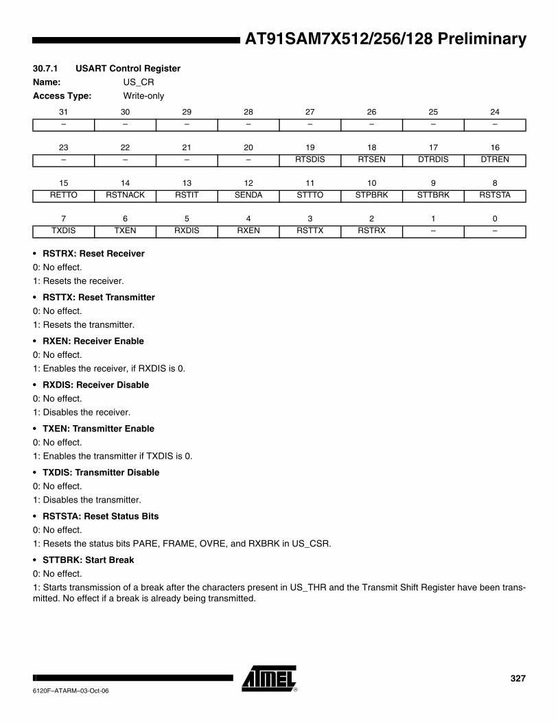
AT91SAM7X512/256/128 Preliminary
30.7.1 USART Control Register
Name: US_CR
Access Type: Write-only
• RSTRX: Reset Receiver
0: No effect.
1: Resets the receiver.
• RSTTX: Reset Transmitter
0: No effect.
1: Resets the transmitter.
• RXEN: Receiver Enable
0: No effect.
1: Enables the receiver, if RXDIS is 0.
• RXDIS: Receiver Disable
0: No effect.
1: Disables the receiver.
• TXEN: Transmitter Enable
0: No effect.
1: Enables the transmitter if TXDIS is 0.
• TXDIS: Transmitter Disable
0: No effect.
1: Disables the transmitter.
• RSTSTA: Reset Status Bits
0: No effect.
1: Resets the status bits PARE, FRAME, OVRE, and RXBRK in US_CSR.
• STTBRK: Start Break
0: No effect.
1: Starts transmission of a break after the characters present in US_THR and the Transmit Shift Register have been trans-mitted. No effect if a break is already being transmitted.
31 30 29 28 27 26 25 24– – – – – – – –
23 22 21 20 19 18 17 16
– – – – RTSDIS RTSEN DTRDIS DTREN
15 14 13 12 11 10 9 8
RETTO RSTNACK RSTIT SENDA STTTO STPBRK STTBRK RSTSTA
7 6 5 4 3 2 1 0
TXDIS TXEN RXDIS RXEN RSTTX RSTRX – –
3276120F–ATARM–03-Oct-06
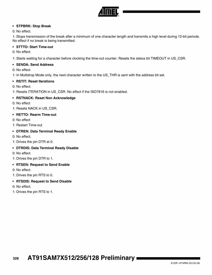
• STPBRK: Stop Break
0: No effect.
1: Stops transmission of the break after a minimum of one character length and transmits a high level during 12-bit periods. No effect if no break is being transmitted.
• STTTO: Start Time-out0: No effect.
1: Starts waiting for a character before clocking the time-out counter. Resets the status bit TIMEOUT in US_CSR.
• SENDA: Send Address
0: No effect.
1: In Multidrop Mode only, the next character written to the US_THR is sent with the address bit set.
• RSTIT: Reset Iterations
0: No effect.
1: Resets ITERATION in US_CSR. No effect if the ISO7816 is not enabled.
• RSTNACK: Reset Non Acknowledge
0: No effect
1: Resets NACK in US_CSR.
• RETTO: Rearm Time-out
0: No effect
1: Restart Time-out
• DTREN: Data Terminal Ready Enable
0: No effect.
1: Drives the pin DTR at 0.
• DTRDIS: Data Terminal Ready Disable
0: No effect.
1: Drives the pin DTR to 1.
• RTSEN: Request to Send Enable
0: No effect.
1: Drives the pin RTS to 0.
• RTSDIS: Request to Send Disable
0: No effect.
1: Drives the pin RTS to 1.
3286120F–ATARM–03-Oct-06
AT91SAM7X512/256/128 Preliminary
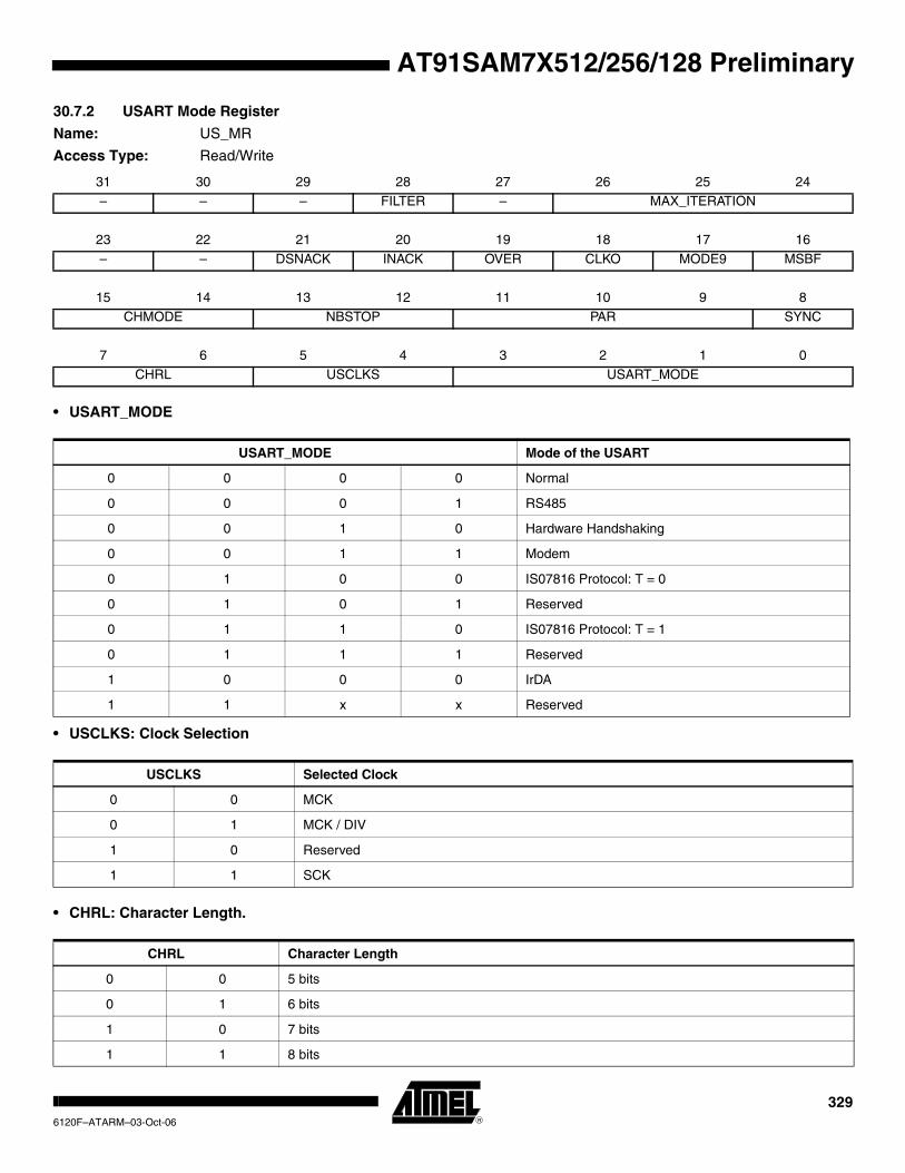
AT91SAM7X512/256/128 Preliminary
30.7.2 USART Mode Register
Name: US_MR
Access Type: Read/Write
• USART_MODE
• USCLKS: Clock Selection
• CHRL: Character Length.
31 30 29 28 27 26 25 24– – – FILTER – MAX_ITERATION
23 22 21 20 19 18 17 16
– – DSNACK INACK OVER CLKO MODE9 MSBF
15 14 13 12 11 10 9 8
CHMODE NBSTOP PAR SYNC
7 6 5 4 3 2 1 0
CHRL USCLKS USART_MODE
USART_MODE Mode of the USART
0 0 0 0 Normal
0 0 0 1 RS485
0 0 1 0 Hardware Handshaking
0 0 1 1 Modem
0 1 0 0 IS07816 Protocol: T = 0
0 1 0 1 Reserved
0 1 1 0 IS07816 Protocol: T = 1
0 1 1 1 Reserved
1 0 0 0 IrDA
1 1 x x Reserved
USCLKS Selected Clock
0 0 MCK
0 1 MCK / DIV
1 0 Reserved
1 1 SCK
CHRL Character Length
0 0 5 bits
0 1 6 bits
1 0 7 bits
1 1 8 bits
3296120F–ATARM–03-Oct-06

• SYNC: Synchronous Mode Select
0: USART operates in Asynchronous Mode.
1: USART operates in Synchronous Mode.
• PAR: Parity Type
• NBSTOP: Number of Stop Bits
• CHMODE: Channel Mode
• MSBF: Bit Order
0: Least Significant Bit is sent/received first.
1: Most Significant Bit is sent/received first.
• MODE9: 9-bit Character Length
0: CHRL defines character length.
1: 9-bit character length.
• CLKO: Clock Output Select
0: The USART does not drive the SCK pin.
1: The USART drives the SCK pin if USCLKS does not select the external clock SCK.
• OVER: Oversampling Mode
0: 16x Oversampling.
1: 8x Oversampling.
PAR Parity Type
0 0 0 Even parity
0 0 1 Odd parity
0 1 0 Parity forced to 0 (Space)
0 1 1 Parity forced to 1 (Mark)
1 0 x No parity
1 1 x Multidrop mode
NBSTOP Asynchronous (SYNC = 0) Synchronous (SYNC = 1)
0 0 1 stop bit 1 stop bit
0 1 1.5 stop bits Reserved
1 0 2 stop bits 2 stop bits
1 1 Reserved Reserved
CHMODE Mode Description
0 0 Normal Mode
0 1 Automatic Echo. Receiver input is connected to the TXD pin.
1 0 Local Loopback. Transmitter output is connected to the Receiver Input..
1 1 Remote Loopback. RXD pin is internally connected to the TXD pin.
3306120F–ATARM–03-Oct-06
AT91SAM7X512/256/128 Preliminary

AT91SAM7X512/256/128 Preliminary
• INACK: Inhibit Non Acknowledge
0: The NACK is generated.
1: The NACK is not generated.
• DSNACK: Disable Successive NACK
0: NACK is sent on the ISO line as soon as a parity error occurs in the received character (unless INACK is set).
1: Successive parity errors are counted up to the value specified in the MAX_ITERATION field. These parity errors gener-ate a NACK on the ISO line. As soon as this value is reached, no additional NACK is sent on the ISO line. The flag ITERATION is asserted.
• MAX_ITERATION
Defines the maximum number of iterations in mode ISO7816, protocol T= 0.
• FILTER: Infrared Receive Line Filter
0: The USART does not filter the receive line.
1: The USART filters the receive line using a three-sample filter (1/16-bit clock) (2 over 3 majority).
3316120F–ATARM–03-Oct-06

30.7.3 USART Interrupt Enable Register
Name: US_IER
Access Type: Write-only
• RXRDY: RXRDY Interrupt Enable
• TXRDY: TXRDY Interrupt Enable
• RXBRK: Receiver Break Interrupt Enable
• ENDRX: End of Receive Transfer Interrupt Enable
• ENDTX: End of Transmit Interrupt Enable
• OVRE: Overrun Error Interrupt Enable
• FRAME: Framing Error Interrupt Enable
• PARE: Parity Error Interrupt Enable
• TIMEOUT: Time-out Interrupt Enable
• TXEMPTY: TXEMPTY Interrupt Enable
• ITERATION: Iteration Interrupt Enable
• TXBUFE: Buffer Empty Interrupt Enable
• RXBUFF: Buffer Full Interrupt Enable
• NACK: Non Acknowledge Interrupt Enable
• RIIC: Ring Indicator Input Change Enable
• DSRIC: Data Set Ready Input Change Enable
• DCDIC: Data Carrier Detect Input Change Interrupt Enable
• CTSIC: Clear to Send Input Change Interrupt Enable
31 30 29 28 27 26 25 24– – – – – – – –
23 22 21 20 19 18 17 16
– – – – CTSIC DCDIC DSRIC RIIC
15 14 13 12 11 10 9 8
– – NACK RXBUFF TXBUFE ITERATION TXEMPTY TIMEOUT
7 6 5 4 3 2 1 0
PARE FRAME OVRE ENDTX ENDRX RXBRK TXRDY RXRDY
3326120F–ATARM–03-Oct-06
AT91SAM7X512/256/128 Preliminary

AT91SAM7X512/256/128 Preliminary
30.7.4 USART Interrupt Disable Register
Name: US_IDR
Access Type: Write-only
• RXRDY: RXRDY Interrupt Disable
• TXRDY: TXRDY Interrupt Disable
• RXBRK: Receiver Break Interrupt Disable
• ENDRX: End of Receive Transfer Interrupt Disable
• ENDTX: End of Transmit Interrupt Disable
• OVRE: Overrun Error Interrupt Disable
• FRAME: Framing Error Interrupt Disable
• PARE: Parity Error Interrupt Disable
• TIMEOUT: Time-out Interrupt Disable
• TXEMPTY: TXEMPTY Interrupt Disable
• ITERATION: Iteration Interrupt Disable
• TXBUFE: Buffer Empty Interrupt Disable
• RXBUFF: Buffer Full Interrupt Disable
• NACK: Non Acknowledge Interrupt Disable
• RIIC: Ring Indicator Input Change Disable
• DSRIC: Data Set Ready Input Change Disable
• DCDIC: Data Carrier Detect Input Change Interrupt Disable
• CTSIC: Clear to Send Input Change Interrupt Disable
31 30 29 28 27 26 25 24– – – – – – – –
23 22 21 20 19 18 17 16
– – – – CTSIC DCDIC DSRIC RIIC
15 14 13 12 11 10 9 8
– – NACK RXBUFF TXBUFE ITERATION TXEMPTY TIMEOUT
7 6 5 4 3 2 1 0
PARE FRAME OVRE ENDTX ENDRX RXBRK TXRDY RXRDY
3336120F–ATARM–03-Oct-06
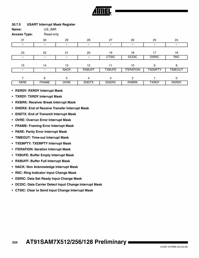
30.7.5 USART Interrupt Mask Register
Name: US_IMR
Access Type: Read-only
• RXRDY: RXRDY Interrupt Mask
• TXRDY: TXRDY Interrupt Mask
• RXBRK: Receiver Break Interrupt Mask
• ENDRX: End of Receive Transfer Interrupt Mask
• ENDTX: End of Transmit Interrupt Mask
• OVRE: Overrun Error Interrupt Mask
• FRAME: Framing Error Interrupt Mask
• PARE: Parity Error Interrupt Mask
• TIMEOUT: Time-out Interrupt Mask
• TXEMPTY: TXEMPTY Interrupt Mask
• ITERATION: Iteration Interrupt Mask
• TXBUFE: Buffer Empty Interrupt Mask
• RXBUFF: Buffer Full Interrupt Mask
• NACK: Non Acknowledge Interrupt Mask
• RIIC: Ring Indicator Input Change Mask
• DSRIC: Data Set Ready Input Change Mask
• DCDIC: Data Carrier Detect Input Change Interrupt Mask
• CTSIC: Clear to Send Input Change Interrupt Mask
31 30 29 28 27 26 25 24– – – – – – – –
23 22 21 20 19 18 17 16
– – – – CTSIC DCDIC DSRIC RIIC
15 14 13 12 11 10 9 8
– – NACK RXBUFF TXBUFE ITERATION TXEMPTY TIMEOUT
7 6 5 4 3 2 1 0
PARE FRAME OVRE ENDTX ENDRX RXBRK TXRDY RXRDY
3346120F–ATARM–03-Oct-06
AT91SAM7X512/256/128 Preliminary

AT91SAM7X512/256/128 Preliminary
30.7.6 USART Channel Status Register
Name: US_CSR
Access Type: Read-only
• RXRDY: Receiver Ready
0: No complete character has been received since the last read of US_RHR or the receiver is disabled. If characters were being received when the receiver was disabled, RXRDY changes to 1 when the receiver is enabled.
1: At least one complete character has been received and US_RHR has not yet been read.
• TXRDY: Transmitter Ready
0: A character is in the US_THR waiting to be transferred to the Transmit Shift Register, or an STTBRK command has been requested, or the transmitter is disabled. As soon as the transmitter is enabled, TXRDY becomes 1.
1: There is no character in the US_THR.
• RXBRK: Break Received/End of Break
0: No Break received or End of Break detected since the last RSTSTA.
1: Break Received or End of Break detected since the last RSTSTA.
• ENDRX: End of Receiver Transfer
0: The End of Transfer signal from the Receive PDC channel is inactive.
1: The End of Transfer signal from the Receive PDC channel is active.
• ENDTX: End of Transmitter Transfer
0: The End of Transfer signal from the Transmit PDC channel is inactive.
1: The End of Transfer signal from the Transmit PDC channel is active.
• OVRE: Overrun Error
0: No overrun error has occurred since the last RSTSTA.
1: At least one overrun error has occurred since the last RSTSTA.
• FRAME: Framing Error
0: No stop bit has been detected low since the last RSTSTA.
1: At least one stop bit has been detected low since the last RSTSTA.
• PARE: Parity Error
0: No parity error has been detected since the last RSTSTA.
1: At least one parity error has been detected since the last RSTSTA.
31 30 29 28 27 26 25 24– – – – – – – –
23 22 21 20 19 18 17 16
CTS DCD DSR RI CTSIC DCDIC DSRIC RIIC
15 14 13 12 11 10 9 8
– – NACK RXBUFF TXBUFE ITERATION TXEMPTY TIMEOUT
7 6 5 4 3 2 1 0
PARE FRAME OVRE ENDTX ENDRX RXBRK TXRDY RXRDY
3356120F–ATARM–03-Oct-06

• TIMEOUT: Receiver Time-out
0: There has not been a time-out since the last Start Time-out command (STTTO in US_CR) or the Time-out Register is 0.
1: There has been a time-out since the last Start Time-out command (STTTO in US_CR).
• TXEMPTY: Transmitter Empty
0: There are characters in either US_THR or the Transmit Shift Register, or the transmitter is disabled.
1: There is at least one character in either US_THR or the Transmit Shift Register.
• ITERATION: Max number of Repetitions Reached
0: Maximum number of repetitions has not been reached since the last RSIT.
1: Maximum number of repetitions has been reached since the last RSIT.
• TXBUFE: Transmission Buffer Empty
0: The signal Buffer Empty from the Transmit PDC channel is inactive.
1: The signal Buffer Empty from the Transmit PDC channel is active.
• RXBUFF: Reception Buffer Full
0: The signal Buffer Full from the Receive PDC channel is inactive.
1: The signal Buffer Full from the Receive PDC channel is active.
• NACK: Non Acknowledge
0: No Non Acknowledge has not been detected since the last RSTNACK.
1: At least one Non Acknowledge has been detected since the last RSTNACK.
• RIIC: Ring Indicator Input Change Flag
0: No input change has been detected on the RI pin since the last read of US_CSR.
1: At least one input change has been detected on the RI pin since the last read of US_CSR.
• DSRIC: Data Set Ready Input Change Flag
0: No input change has been detected on the DSR pin since the last read of US_CSR.
1: At least one input change has been detected on the DSR pin since the last read of US_CSR.
• DCDIC: Data Carrier Detect Input Change Flag
0: No input change has been detected on the DCD pin since the last read of US_CSR.
1: At least one input change has been detected on the DCD pin since the last read of US_CSR.
• CTSIC: Clear to Send Input Change Flag
0: No input change has been detected on the CTS pin since the last read of US_CSR.
1: At least one input change has been detected on the CTS pin since the last read of US_CSR.
• RI: Image of RI Input
0: RI is at 0.
1: RI is at 1.
• DSR: Image of DSR Input
0: DSR is at 0
1: DSR is at 1.
• DCD: Image of DCD Input
0: DCD is at 0.
1: DCD is at 1.
3366120F–ATARM–03-Oct-06
AT91SAM7X512/256/128 Preliminary
AT91SAM7X512/256/128 Preliminary
• CTS: Image of CTS Input
0: CTS is at 0.
1: CTS is at 1.
3376120F–ATARM–03-Oct-06

30.7.7 USART Receive Holding Register
Name: US_RHR
Access Type: Read-only
• RXCHR: Received Character
Last character received if RXRDY is set.
• RXSYNH: Received Sync
0: Last Character received is a Data.
1: Last Character received is a Command.
30.7.8 USART Transmit Holding Register
Name: US_THR
Access Type: Write-only
• TXCHR: Character to be Transmitted
Next character to be transmitted after the current character if TXRDY is not set.
• TXSYNH: Sync Field to be transmitted
0: The next character sent is encoded as a data. Start Frame Delimiter is DATA SYNC.
1: The next character sent is encoded as a command. Start Frame Delimiter is COMMAND SYNC.
31 30 29 28 27 26 25 24– – – – – – – –
23 22 21 20 19 18 17 16
– – – – – – – –
15 14 13 12 11 10 9 8
RXSYNH – – – – – – RXCHR
7 6 5 4 3 2 1 0
RXCHR
31 30 29 28 27 26 25 24
– – – – – – – –
23 22 21 20 19 18 17 16
– – – – – – – –
15 14 13 12 11 10 9 8
TXSYNH – – – – – – TXCHR
7 6 5 4 3 2 1 0
TXCHR
3386120F–ATARM–03-Oct-06
AT91SAM7X512/256/128 Preliminary
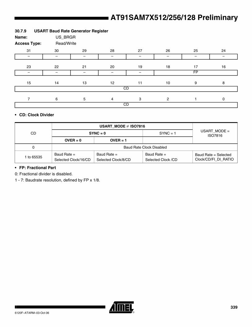
AT91SAM7X512/256/128 Preliminary
30.7.9 USART Baud Rate Generator Register
Name: US_BRGR
Access Type: Read/Write
• CD: Clock Divider
• FP: Fractional Part
0: Fractional divider is disabled.
1 - 7: Baudrate resolution, defined by FP x 1/8.
31 30 29 28 27 26 25 24– – – – – – – –
23 22 21 20 19 18 17 16
– – – – – FP
15 14 13 12 11 10 9 8
CD
7 6 5 4 3 2 1 0
CD
CD
USART_MODE ≠ ISO7816USART_MODE =
ISO7816SYNC = 0 SYNC = 1
OVER = 0 OVER = 1
0 Baud Rate Clock Disabled
1 to 65535Baud Rate =
Selected Clock/16/CD
Baud Rate =
Selected Clock/8/CD
Baud Rate =
Selected Clock /CDBaud Rate = Selected Clock/CD/FI_DI_RATIO
3396120F–ATARM–03-Oct-06
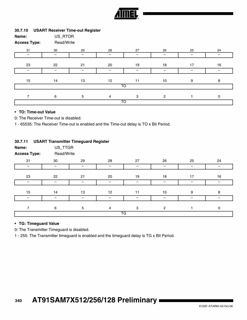
30.7.10 USART Receiver Time-out Register
Name: US_RTOR
Access Type: Read/Write
• TO: Time-out Value
0: The Receiver Time-out is disabled.
1 - 65535: The Receiver Time-out is enabled and the Time-out delay is TO x Bit Period.
30.7.11 USART Transmitter Timeguard Register
Name: US_TTGR
Access Type: Read/Write
• TG: Timeguard Value
0: The Transmitter Timeguard is disabled.
1 - 255: The Transmitter timeguard is enabled and the timeguard delay is TG x Bit Period.
31 30 29 28 27 26 25 24– – – – – – – –
23 22 21 20 19 18 17 16
– – – – – – – –
15 14 13 12 11 10 9 8
TO
7 6 5 4 3 2 1 0
TO
31 30 29 28 27 26 25 24
– – – – – – – –
23 22 21 20 19 18 17 16
– – – – – – – –
15 14 13 12 11 10 9 8
– – – – – – – –
7 6 5 4 3 2 1 0
TG
3406120F–ATARM–03-Oct-06
AT91SAM7X512/256/128 Preliminary
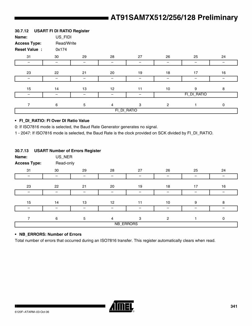
AT91SAM7X512/256/128 Preliminary
30.7.12 USART FI DI RATIO Register
Name: US_FIDI
Access Type: Read/Write
Reset Value : 0x174
• FI_DI_RATIO: FI Over DI Ratio Value
0: If ISO7816 mode is selected, the Baud Rate Generator generates no signal.
1 - 2047: If ISO7816 mode is selected, the Baud Rate is the clock provided on SCK divided by FI_DI_RATIO.
30.7.13 USART Number of Errors Register
Name: US_NER
Access Type: Read-only
• NB_ERRORS: Number of Errors
Total number of errors that occurred during an ISO7816 transfer. This register automatically clears when read.
31 30 29 28 27 26 25 24
– – – – – – – –
23 22 21 20 19 18 17 16
– – – – – – – –
15 14 13 12 11 10 9 8
– – – – – FI_DI_RATIO
7 6 5 4 3 2 1 0
FI_DI_RATIO
31 30 29 28 27 26 25 24
– – – – – – – –
23 22 21 20 19 18 17 16
– – – – – – – –
15 14 13 12 11 10 9 8
– – – – – – – –
7 6 5 4 3 2 1 0
NB_ERRORS
3416120F–ATARM–03-Oct-06
30.7.14 USART IrDA FILTER Register
Name: US_IF
Access Type: Read/Write
• IRDA_FILTER: IrDA Filter
Sets the filter of the IrDA demodulator.
31 30 29 28 27 26 25 24– – – – – – – –
23 22 21 20 19 18 17 16
– – – – – – – –
15 14 13 12 11 10 9 8
– – – – – – – –
7 6 5 4 3 2 1 0
IRDA_FILTER
3426120F–ATARM–03-Oct-06
AT91SAM7X512/256/128 Preliminary
AT91SAM7X512/256/128 Preliminary
31. Synchronous Serial Controller (SSC)
31.1 OverviewThe Atmel Synchronous Serial Controller (SSC) provides a synchronous communication link with external devices. It supports many serial synchronous communication protocols generally used in audio and telecom applications such as I2S, Short Frame Sync, Long Frame Sync, etc.
The SSC contains an independent receiver and transmitter and a common clock divider. The receiver and the transmitter each interface with three signals: the TD/RD signal for data, the TK/RK signal for the clock and the TF/RF signal for the Frame Sync. The transfers can be pro-grammed to start automatically or on different events detected on the Frame Sync signal.
The SSC’s high-level of programmability and its two dedicated PDC channels of up to 32 bits permit a continuous high bit rate data transfer without processor intervention.
Featuring connection to two PDC channels, the SSC permits interfacing with low processor overhead to the following:
• CODEC’s in master or slave mode
• DAC through dedicated serial interface, particularly I2S
• Magnetic card reader
3436120F–ATARM–03-Oct-06

31.2 Block Diagram
Figure 31-1. Block Diagram
31.3 Application Block Diagram
Figure 31-2. Application Block Diagram
SSC Interface PIO
PDC
APB Bridge
MCK
ASB
APB
TF
TK
TD
RF
RK
RDInterrupt Control
SSC Interrupt
PMC
InterruptManagement
Power Management
TestManagement
SSC
Serial AUDIO
OS or RTOS Driver
Codec FrameManagement
Line Interface Time SlotManagement
3446120F–ATARM–03-Oct-06
AT91SAM7X512/256/128 Preliminary

AT91SAM7X512/256/128 Preliminary
31.4 Pin Name List
31.5 Product Dependencies
31.5.1 I/O LinesThe pins used for interfacing the compliant external devices may be multiplexed with PIO lines.
Before using the SSC receiver, the PIO controller must be configured to dedicate the SSC receiver I/O lines to the SSC peripheral mode.
Before using the SSC transmitter, the PIO controller must be configured to dedicate the SSC transmitter I/O lines to the SSC peripheral mode.
31.5.2 Power ManagementThe SSC is not continuously clocked. The SSC interface may be clocked through the Power Management Controller (PMC), therefore the programmer must first configure the PMC to enable the SSC clock.
31.5.3 InterruptThe SSC interface has an interrupt line connected to the Advanced Interrupt Controller (AIC). Handling interrupts requires programming the AIC before configuring the SSC.
All SSC interrupts can be enabled/disabled configuring the SSC Interrupt mask register. Each pending and unmasked SSC interrupt will assert the SSC interrupt line. The SSC interrupt ser-vice routine can get the interrupt origin by reading the SSC interrupt status register.
31.6 Functional DescriptionThis chapter contains the functional description of the following: SSC Functional Block, Clock Management, Data format, Start, Transmitter, Receiver and Frame Sync.
The receiver and transmitter operate separately. However, they can work synchronously by programming the receiver to use the transmit clock and/or to start a data transfer when trans-mission starts. Alternatively, this can be done by programming the transmitter to use the receive clock and/or to start a data transfer when reception starts. The transmitter and the receiver can be programmed to operate with the clock signals provided on either the TK or RK pins. This allows the SSC to support many slave-mode data transfers. The maximum clock speed allowed on the TK and RK pins is the master clock divided by 2.
Table 31-1. I/O Lines Description
Pin Name Pin Description Type
RF Receiver Frame Synchro Input/Output
RK Receiver Clock Input/Output
RD Receiver Data Input
TF Transmitter Frame Synchro Input/Output
TK Transmitter Clock Input/Output
TD Transmitter Data Output
3456120F–ATARM–03-Oct-06
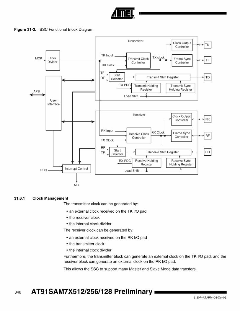
Figure 31-3. SSC Functional Block Diagram
31.6.1 Clock ManagementThe transmitter clock can be generated by:
• an external clock received on the TK I/O pad
• the receiver clock
• the internal clock divider
The receiver clock can be generated by:
• an external clock received on the RK I/O pad
• the transmitter clock
• the internal clock divider
Furthermore, the transmitter block can generate an external clock on the TK I/O pad, and the receiver block can generate an external clock on the RK I/O pad.
This allows the SSC to support many Master and Slave Mode data transfers.
Interrupt Control
AIC
UserInterface
APB
MCK
Receive ClockController
StartSelector
TX Clock
RK Input
RF
TF
Clock OutputController
Frame SyncController
Transmit ClockController
Transmit Shift RegisterStart
Selector
Transmit SyncHolding Register
Transmit HoldingRegister
Load Shift
RX clock
TX clockTK Input
TF
TX PDC
RF
RD
RF
RKClock Output
Controller
Frame SyncController
Receive Shift Register
Receive SyncHolding Register
Receive HoldingRegister
Load Shift
TD
TF
TK
RX Clock
RX PDC
Receiver
PDC
Transmitter
ClockDivider
3466120F–ATARM–03-Oct-06
AT91SAM7X512/256/128 Preliminary

AT91SAM7X512/256/128 Preliminary
31.6.1.1 Clock Divider
Figure 31-4. Divided Clock Block Diagram
The Master Clock divider is determined by the 12-bit field DIV counter and comparator (so its maximal value is 4095) in the Clock Mode Register SSC_CMR, allowing a Master Clock divi-sion by up to 8190. The Divided Clock is provided to both the Receiver and Transmitter. When this field is programmed to 0, the Clock Divider is not used and remains inactive.
When DIV is set to a value equal to or greater than 1, the Divided Clock has a frequency of Master Clock divided by 2 times DIV. Each level of the Divided Clock has a duration of the Master Clock multiplied by DIV. This ensures a 50% duty cycle for the Divided Clock regard-less of whether the DIV value is even or odd.
Figure 31-5. Divided Clock Generation
31.6.1.2 Transmitter Clock ManagementThe transmitter clock is generated from the receiver clock or the divider clock or an external clock scanned on the TK I/O pad. The transmitter clock is selected by the CKS field in SSC_TCMR (Transmit Clock Mode Register). Transmit Clock can be inverted independently by the CKI bits in SSC_TCMR.
The transmitter can also drive the TK I/O pad continuously or be limited to the actual data transfer. The clock output is configured by the SSC_TCMR register. The Transmit Clock Inver-sion (CKI) bits have no effect on the clock outputs. Programming the TCMR register to select
MCK Divided Clock
Clock Divider
/ 2 12-bit Counter
SSC_CMR
Master Clock
Divided ClockDIV = 1
Master Clock
Divided ClockDIV = 3
Divided Clock Frequency = MCK/2
Divided Clock Frequency = MCK/6
Table 31-2.
Maximum Minimum
MCK / 2 MCK / 8190
3476120F–ATARM–03-Oct-06

TK pin (CKS field) and at the same time Continuous Transmit Clock (CKO field) might lead to unpredictable results.
Figure 31-6. Transmitter Clock Management
31.6.1.3 Receiver Clock ManagementThe receiver clock is generated from the transmitter clock or the divider clock or an external clock scanned on the RK I/O pad. The Receive Clock is selected by the CKS field in SSC_RCMR (Receive Clock Mode Register). Receive Clocks can be inverted independently by the CKI bits in SSC_RCMR.
The receiver can also drive the RK I/O pad continuously or be limited to the actual data trans-fer. The clock output is configured by the SSC_RCMR register. The Receive Clock Inversion (CKI) bits have no effect on the clock outputs. Programming the RCMR register to select RK pin (CKS field) and at the same time Continuous Receive Clock (CKO field) can lead to unpre-dictable results.
Figure 31-7. Receiver Clock Management
31.6.1.4 Serial Clock Ratio ConsiderationsThe Transmitter and the Receiver can be programmed to operate with the clock signals pro-vided on either the TK or RK pins. This allows the SSC to support many slave-mode data transfers. In this case, the maximum clock speed allowed on the RK pin is:
– Master Clock divided by 2 if Receiver Frame Synchro is input
– Master Clock divided by 3 if Receiver Frame Synchro is output
In addition, the maximum clock speed allowed on the TK pin is:
– Master Clock divided by 6 if Transmit Frame Synchro is input
– Master Clock divided by 2 if Transmit Frame Synchro is output
Receiver Clock
Divider ClockTransmitter Clock
SSC_TCMR.CKI
SSC_TCMR.CKS
TK
SSC_TCMR.CKO
1
0
TK
Transmitter Clock
Divider ClockReceiver Clock
SSC_RCMR.CKI
SSC_RCMR.CKS
RK
SSC_RCMR.CKO
1
0
RK
3486120F–ATARM–03-Oct-06
AT91SAM7X512/256/128 Preliminary

AT91SAM7X512/256/128 Preliminary
31.6.2 Transmitter OperationsA transmitted frame is triggered by a start event and can be followed by synchronization data before data transmission.
The start event is configured by setting the Transmit Clock Mode Register (SSC_TCMR). See “Start” on page 350.
The frame synchronization is configured setting the Transmit Frame Mode Register (SSC_TFMR). See “Frame Sync” on page 352.
To transmit data, the transmitter uses a shift register clocked by the transmitter clock signal and the start mode selected in the SSC_TCMR. Data is written by the application to the SSC_THR register then transferred to the shift register according to the data format selected.
When both the SSC_THR and the transmit shift register are empty, the status flag TXEMPTY is set in SSC_SR. When the Transmit Holding register is transferred in the Transmit shift reg-ister, the status flag TXRDY is set in SSC_SR and additional data can be loaded in the holding register.
Figure 31-8. Transmitter Block Diagram
31.6.3 Receiver OperationsA received frame is triggered by a start event and can be followed by synchronization data before data transmission.
The start event is configured setting the Receive Clock Mode Register (SSC_RCMR). See “Start” on page 350.
The frame synchronization is configured setting the Receive Frame Mode Register (SSC_RFMR). See “Frame Sync” on page 352.
The receiver uses a shift register clocked by the receiver clock signal and the start mode selected in the SSC_RCMR. The data is transferred from the shift register depending on the data format selected.
Transmit Shift RegisterStartSelector
SSC_TSHRSSC_THR
Transmitter Clock
TD
SSC_TFMR.FSLENSSC_TFMR.DATLEN
SSC_CR.TXEN
SSC_CR.TXDIS
SSC_TCMR.STTDLYSSC_TFMR.FSDENSSC_TFMR.DATNB
SSC_SR.TXEN
SSC_TFMR.DATDEF
SSC_TFMR.MSBF
SSC_TCMR.STTDLYSSC_TFMR.FSDEN
0
1
10
RF TF
3496120F–ATARM–03-Oct-06

When the receiver shift register is full, the SSC transfers this data in the holding register, the status flag RXRDY is set in SSC_SR and the data can be read in the receiver holding register. If another transfer occurs before read of the RHR register, the status flag OVERUN is set in SSC_SR and the receiver shift register is transferred in the RHR register.
Figure 31-9. Receiver Block Diagram
31.6.4 StartThe transmitter and receiver can both be programmed to start their operations when an event occurs, respectively in the Transmit Start Selection (START) field of SSC_TCMR and in the Receive Start Selection (START) field of SSC_RCMR.
Under the following conditions the start event is independently programmable:
• Continuous. In this case, the transmission starts as soon as a word is written in SSC_THR and the reception starts as soon as the Receiver is enabled.
• Synchronously with the transmitter/receiver
• On detection of a falling/rising edge on TF/RF
• On detection of a low level/high level on TF/RF
• On detection of a level change or an edge on TF/RF
A start can be programmed in the same manner on either side of the Transmit/Receive Clock Register (RCMR/TCMR). Thus, the start could be on TF (Transmit) or RF (Receive).
Moreover, the Receiver can start when data is detected in the bit stream with the Compare Functions.
Detection on TF/RF input/output is done by the field FSOS of the Transmit/Receive Frame Mode Register (TFMR/RFMR).
Receive Shift RegisterStartSelector
SSC_RHRSSC_RSHR
Receiver ClockRD
SSC_RFMR.FSLEN SSC_RFMR.DATLEN
RF
SSC_CR.RXEN
SSC_CR.RXDIS
SSC_SR.RXEN
SSC_RFMR.MSBF
SSC_RCMR.STTDLY
SSC_RFMR.DATNBTF
3506120F–ATARM–03-Oct-06
AT91SAM7X512/256/128 Preliminary

AT91SAM7X512/256/128 Preliminary
Figure 31-10. Transmit Start Mode
Figure 31-11. Receive Pulse/Edge Start Modes
X
TK
TF(Input)
TD(Output)
TD(Output)
TD(Output)
TD(Output)
TD(Output)
TD(Output)
X BO B1
X BO B1
BO B1
BO B1
BO B1BO B1
BO B1B1BO
X
X
X
STTDLY
STTDLY
STTDLY
STTDLY
STTDLY
STTDLYStart = Falling Edge on TF
Start = Rising Edge on TF
Start = Low Level on TF
Start = High Level on TF
Start = Any Edge on TF
Start = Level Change on TF
X
RK
RF(Input)
RD(Input)
RD(Input)
RD(Input)
RD(Input)
RD(Input)
RD(Input)
X BO B1
X BO B1
BO B1
BO B1
BO B1BO B1
BO B1B1BO
X
X
X
STTDLY
STTDLY
STTDLY
STTDLY
STTDLY
STTDLYStart = Falling Edge on RF
Start = Rising Edge on RF
Start = Low Level on RF
Start = High Level on RF
Start = Any Edge on RF
Start = Level Change on RF
3516120F–ATARM–03-Oct-06

31.6.5 Frame SyncThe Transmitter and Receiver Frame Sync pins, TF and RF, can be programmed to generate different kinds of frame synchronization signals. The Frame Sync Output Selection (FSOS) field in the Receive Frame Mode Register (SSC_RFMR) and in the Transmit Frame Mode Register (SSC_TFMR) are used to select the required waveform.
• Programmable low or high levels during data transfer are supported.
• Programmable high levels before the start of data transfers or toggling are also supported.
If a pulse waveform is selected, the Frame Sync Length (FSLEN) field in SSC_RFMR and SSC_TFMR programs the length of the pulse, from 1 bit time up to 16 bit time.
The periodicity of the Receive and Transmit Frame Sync pulse output can be programmed through the Period Divider Selection (PERIOD) field in SSC_RCMR and SSC_TCMR.
31.6.5.1 Frame Sync DataFrame Sync Data transmits or receives a specific tag during the Frame Sync signal.
During the Frame Sync signal, the Receiver can sample the RD line and store the data in the Receive Sync Holding Register and the transmitter can transfer Transmit Sync Holding Regis-ter in the Shifter Register. The data length to be sampled/shifted out during the Frame Sync signal is programmed by the FSLEN field in SSC_RFMR/SSC_TFMR.
Concerning the Receive Frame Sync Data operation, if the Frame Sync Length is equal to or lower than the delay between the start event and the actual data reception, the data sampling operation is performed in the Receive Sync Holding Register through the Receive Shift Register.
The Transmit Frame Sync Operation is performed by the transmitter only if the bit Frame Sync Data Enable (FSDEN) in SSC_TFMR is set. If the Frame Sync length is equal to or lower than the delay between the start event and the actual data transmission, the normal transmission has priority and the data contained in the Transmit Sync Holding Register is transferred in the Transmit Register, then shifted out.
31.6.5.2 Frame Sync Edge DetectionThe Frame Sync Edge de tec t i on i s p rogrammed by the FSEDGE f ie ld i n SSC_RFMR/SSC_TFMR. This sets the corresponding flags RXSYN/TXSYN in the SSC Sta-tus Register (SSC_SR) on frame synchro edge detection (signals RF/TF).
31.6.6 Receive Compare Modes
Figure 31-12. Receive Compare Modes
CMP0 CMP3CMP2CMP1 Ignored B0 B2B1
Start
RK
RD(Input)
FSLENUp to 16 Bits
(4 in This Example)
STDLY DATLEN
3526120F–ATARM–03-Oct-06
AT91SAM7X512/256/128 Preliminary

AT91SAM7X512/256/128 Preliminary
31.6.6.1 Compare FunctionsCompare 0 can be one start event of the Receiver. In this case, the receiver compares at each new sample the last FSLEN bits received at the FSLEN lower bit of the data contained in the Compare 0 Register (SSC_RC0R). When this start event is selected, the user can program the Receiver to start a new data transfer either by writing a new Compare 0, or by receiving continuously until Compare 1 occurs. This selection is done with the bit (STOP) in SSC_RCMR.
31.6.7 Data FormatThe data framing format of both the transmitter and the receiver are programmable through the Transmitter Frame Mode Register (SSC_TFMR) and the Receiver Frame Mode Register (SSC_RFMR). In either case, the user can independently select:
• the event that starts the data transfer (START)
• the delay in number of bit periods between the start event and the first data bit (STTDLY)
• the length of the data (DATLEN)
• the number of data to be transferred for each start event (DATNB).
• the length of synchronization transferred for each start event (FSLEN)
• the bit sense: most or lowest significant bit first (MSBF).
Additionally, the transmitter can be used to transfer synchronization and select the level driven on the TD pin while not in data transfer operation. This is done respectively by the Frame Sync Data Enable (FSDEN) and by the Data Default Value (DATDEF) bits in SSC_TFMR.
3536120F–ATARM–03-Oct-06

Figure 31-13. Transmit and Receive Frame Format in Edge/Pulse Start Modes
Note: 1. Example of input on falling edge of TF/RF.
Table 31-3. Data Frame Registers
Transmitter Receiver Field Length Comment
SSC_TFMR SSC_RFMR DATLEN Up to 32 Size of word
SSC_TFMR SSC_RFMR DATNB Up to 16 Number of words transmitted in frame
SSC_TFMR SSC_RFMR MSBF Most significant bit first
SSC_TFMR SSC_RFMR FSLEN Up to 16 Size of Synchro data register
SSC_TFMR DATDEF 0 or 1 Data default value ended
SSC_TFMR FSDEN Enable send SSC_TSHR
SSC_TCMR SSC_RCMR PERIOD Up to 512 Frame size
SSC_TCMR SSC_RCMR STTDLY Up to 255 Size of transmit start delay
Sync Data Default
STTDLY
Sync Data IgnoredRD
Default
Data
DATLEN
Data
Data
Data
DATLEN
Data
Data Default
Default
Ignored
Sync Data
Sync Data
FSLEN
TF/RF(1)
StartStart
From SSC_TSHR From SSC_THR
From SSC_THR
From SSC_THR
From SSC_THR
To SSC_RHR To SSC_RHRTo SSC_RSHR
TD(If FSDEN = 0)
TD(If FSDEN = 1)
DATNB
PERIOD
FromDATDEF FromDATDEF
From DATDEF From DATDEF
3546120F–ATARM–03-Oct-06
AT91SAM7X512/256/128 Preliminary
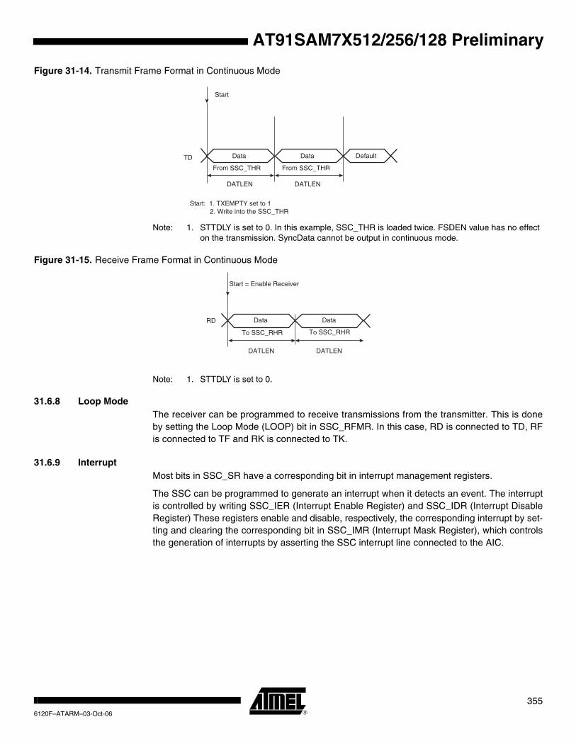
AT91SAM7X512/256/128 Preliminary
Figure 31-14. Transmit Frame Format in Continuous Mode
Note: 1. STTDLY is set to 0. In this example, SSC_THR is loaded twice. FSDEN value has no effect on the transmission. SyncData cannot be output in continuous mode.
Figure 31-15. Receive Frame Format in Continuous Mode
Note: 1. STTDLY is set to 0.
31.6.8 Loop ModeThe receiver can be programmed to receive transmissions from the transmitter. This is done by setting the Loop Mode (LOOP) bit in SSC_RFMR. In this case, RD is connected to TD, RF is connected to TF and RK is connected to TK.
31.6.9 InterruptMost bits in SSC_SR have a corresponding bit in interrupt management registers.
The SSC can be programmed to generate an interrupt when it detects an event. The interrupt is controlled by writing SSC_IER (Interrupt Enable Register) and SSC_IDR (Interrupt Disable Register) These registers enable and disable, respectively, the corresponding interrupt by set-ting and clearing the corresponding bit in SSC_IMR (Interrupt Mask Register), which controls the generation of interrupts by asserting the SSC interrupt line connected to the AIC.
DATLEN
Data
DATLEN
Data Default
Start
From SSC_THR From SSC_THR
TD
Start: 1. TXEMPTY set to 1 2. Write into the SSC_THR
Data
DATLEN
Data
DATLEN
Start = Enable Receiver
To SSC_RHR To SSC_RHR
RD
3556120F–ATARM–03-Oct-06

Figure 31-16. Interrupt Block Diagram
31.7 SSC Application ExamplesThe SSC can support several serial communication modes used in audio or high speed serial links. Some standard applications are shown in the following figures. All serial link applications supported by the SSC are not listed here.
Figure 31-17. Audio Application Block Diagram
SSC_IMR
PDC
Interrupt Control
SSC Interrupt
Set
RXRDYOVRUN
RXSYNC
Receiver
Transmitter
TXRDYTXEMPTYTXSYNC
TXBUFE
ENDTX
RXBUFFENDRX
Clear
SSC_IER SSC_IDR
SSC
RK
RF
RD
TD
TF
TKClock SCK
Word Select WS
Data SD
I2S RECEIVER
Clock SCK
Word Select WS
Data SD
Right ChannelLeft Channel
MSB MSBLSB
3566120F–ATARM–03-Oct-06
AT91SAM7X512/256/128 Preliminary
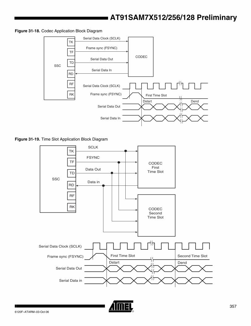
AT91SAM7X512/256/128 Preliminary
Figure 31-18. Codec Application Block Diagram
Figure 31-19. Time Slot Application Block Diagram
SSC
RK
RF
RD
TD
TF
TKSerial Data Clock (SCLK)
Frame sync (FSYNC)
Serial Data Out
Serial Data In
CODEC
Serial Data Clock (SCLK)
Frame sync (FSYNC)
Serial Data Out
Serial Data In
First Time Slot
Dstart Dend
SSC
RK
RF
RD
TD
TF
TKSCLK
FSYNC
Data Out
Data in
CODECFirst
Time Slot
Serial Data Clock (SCLK)
Frame sync (FSYNC)
Serial Data Out
Serial Data in
CODECSecond
Time Slot
First Time Slot Second Time Slot
Dstart Dend
3576120F–ATARM–03-Oct-06

AT91SAM7X512/256/128 Preliminary
31.8 Synchronous Serial Controller (SSC) User Interface
Table 31-4. Register Mapping
Offset Register Register Name Access Reset
0x0 Control Register SSC_CR Write –
0x4 Clock Mode Register SSC_CMR Read/Write 0x0
0x8 Reserved – – –
0xC Reserved – – –
0x10 Receive Clock Mode Register SSC_RCMR Read/Write 0x0
0x14 Receive Frame Mode Register SSC_RFMR Read/Write 0x0
0x18 Transmit Clock Mode Register SSC_TCMR Read/Write 0x0
0x1C Transmit Frame Mode Register SSC_TFMR Read/Write 0x0
0x20 Receive Holding Register SSC_RHR Read 0x0
0x24 Transmit Holding Register SSC_THR Write –
0x28 Reserved – – –
0x2C Reserved – – –
0x30 Receive Sync. Holding Register SSC_RSHR Read 0x0
0x34 Transmit Sync. Holding Register SSC_TSHR Read/Write 0x0
0x38 Receive Compare 0 Register SSC_RC0R Read/Write 0x0
0x3C Receive Compare 1 Register SSC_RC1R Read/Write 0x0
0x40 Status Register SSC_SR Read 0x000000CC
0x44 Interrupt Enable Register SSC_IER Write –
0x48 Interrupt Disable Register SSC_IDR Write –
0x4C Interrupt Mask Register SSC_IMR Read 0x0
0x50-0xFC Reserved – – –
0x100- 0x124 Reserved for Peripheral Data Controller (PDC) – – –
3586120F–ATARM–03-Oct-06
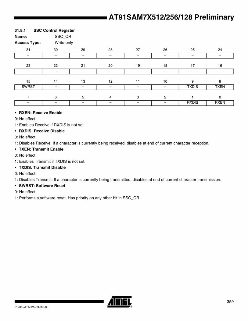
AT91SAM7X512/256/128 Preliminary
31.8.1 SSC Control Register
Name: SSC_CR
Access Type: Write-only
• RXEN: Receive Enable
0: No effect.
1: Enables Receive if RXDIS is not set.
• RXDIS: Receive Disable
0: No effect.
1: Disables Receive. If a character is currently being received, disables at end of current character reception.
• TXEN: Transmit Enable
0: No effect.
1: Enables Transmit if TXDIS is not set.
• TXDIS: Transmit Disable
0: No effect.
1: Disables Transmit. If a character is currently being transmitted, disables at end of current character transmission.
• SWRST: Software Reset
0: No effect.
1: Performs a software reset. Has priority on any other bit in SSC_CR.
31 30 29 28 27 26 25 24– – – – – – – –
23 22 21 20 19 18 17 16
– – – – – – – –
15 14 13 12 11 10 9 8
SWRST – – – – – TXDIS TXEN
7 6 5 4 3 2 1 0
– – – – – – RXDIS RXEN
3596120F–ATARM–03-Oct-06
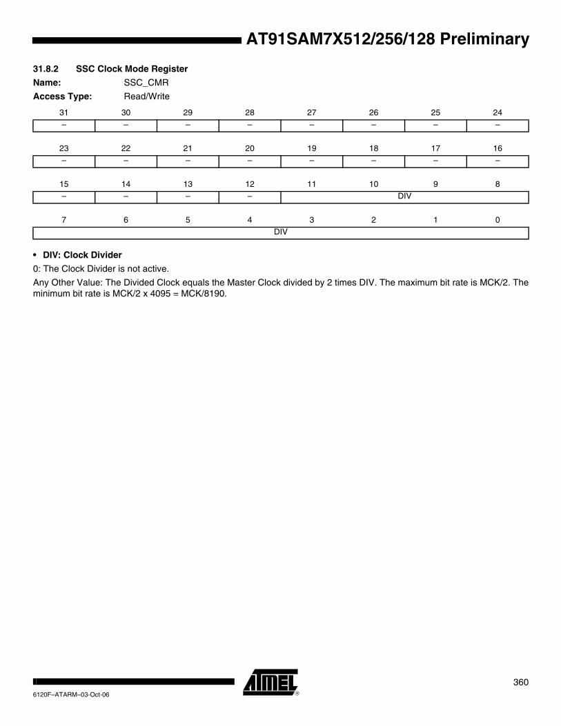
AT91SAM7X512/256/128 Preliminary
31.8.2 SSC Clock Mode Register
Name: SSC_CMR
Access Type: Read/Write
• DIV: Clock Divider
0: The Clock Divider is not active.
Any Other Value: The Divided Clock equals the Master Clock divided by 2 times DIV. The maximum bit rate is MCK/2. The minimum bit rate is MCK/2 x 4095 = MCK/8190.
31 30 29 28 27 26 25 24– – – – – – – –
23 22 21 20 19 18 17 16
– – – – – – – –
15 14 13 12 11 10 9 8
– – – – DIV
7 6 5 4 3 2 1 0
DIV
3606120F–ATARM–03-Oct-06

AT91SAM7X512/256/128 Preliminary
31.8.3 SSC Receive Clock Mode Register
Name: SSC_RCMR
Access Type: Read/Write
• CKS: Receive Clock Selection
• CKO: Receive Clock Output Mode Selection
• CKI: Receive Clock Inversion
0: The data inputs (Data and Frame Sync signals) are sampled on Receive Clock falling edge. The Frame Sync signal out-put is shifted out on Receive Clock rising edge.
1: The data inputs (Data and Frame Sync signals) are sampled on Receive Clock rising edge. The Frame Sync signal out-put is shifted out on Receive Clock falling edge.
CKI affects only the Receive Clock and not the output clock signal.
31 30 29 28 27 26 25 24PERIOD
23 22 21 20 19 18 17 16
STDDLY
15 14 13 12 11 10 9 8
– – – STOP START
7 6 5 4 3 2 1 0
CKG CKI CKO CKS
CKS Selected Receive Clock
0x0 Divided Clock
0x1 TK Clock signal
0x2 RK pin
0x3 Reserved
CKO Receive Clock Output Mode RK pin
0x0 None Input-only
0x1 Continuous Receive Clock Output
0x2 Receive Clock only during data transfers Output
0x3-0x7 Reserved
3616120F–ATARM–03-Oct-06

AT91SAM7X512/256/128 Preliminary
• CKG: Receive Clock Gating Selection
• START: Receive Start Selection
• STOP: Receive Stop Selection
0: After completion of a data transfer when starting with a Compare 0, the receiver stops the data transfer and waits for a new compare 0.
1: After starting a receive with a Compare 0, the receiver operates in a continuous mode until a Compare 1 is detected.
• STTDLY: Receive Start Delay
If STTDLY is not 0, a delay of STTDLY clock cycles is inserted between the start event and the actual start of reception. When the Receiver is programmed to start synchronously with the Transmitter, the delay is also applied.
Note: It is very important that STTDLY be set carefully. If STTDLY must be set, it should be done in relation to TAG (Receive Sync Data) reception.
• PERIOD: Receive Period Divider Selection
This field selects the divider to apply to the selected Receive Clock in order to generate a new Frame Sync Signal. If 0, no PERIOD signal is generated. If not 0, a PERIOD signal is generated each 2 x (PERIOD+1) Receive Clock.
CKG Receive Clock Gating
0x0 None, continuous clock
0x1 Receive Clock enabled only if RF Low
0x2 Receive Clock enabled only if RF High
0x3 Reserved
START Receive Start
0x0Continuous, as soon as the receiver is enabled, and immediately after the end of transfer of the previous data.
0x1 Transmit start
0x2 Detection of a low level on RF signal
0x3 Detection of a high level on RF signal
0x4 Detection of a falling edge on RF signal
0x5 Detection of a rising edge on RF signal
0x6 Detection of any level change on RF signal
0x7 Detection of any edge on RF signal
0x8 Compare 0
0x9-0xF Reserved
3626120F–ATARM–03-Oct-06

AT91SAM7X512/256/128 Preliminary
31.8.4 SSC Receive Frame Mode Register
Name: SSC_RFMR
Access Type: Read/Write
• DATLEN: Data Length
0: Forbidden value (1-bit data length not supported). Any other value: The bit stream contains DATLEN + 1 data bits. Moreover, it defines the transfer size performed by the PDC2 assigned to the Receiver. If DATLEN is lower or equal to 7, data transfers are in bytes. If DATLEN is between 8 and 15 (included), half-words are transferred, and for any other value, 32-bit words are transferred.
• LOOP: Loop Mode
0: Normal operating mode.
1: RD is driven by TD, RF is driven by TF and TK drives RK.
• MSBF: Most Significant Bit First
0: The lowest significant bit of the data register is sampled first in the bit stream.
1: The most significant bit of the data register is sampled first in the bit stream.
• DATNB: Data Number per Frame
This field defines the number of data words to be received after each transfer start, which is equal to (DATNB + 1).
• FSLEN: Receive Frame Sync Length
This field defines the length of the Receive Frame Sync Signal and the number of bits sampled and stored in the Receive Sync Data Register. When this mode is selected by the START field in the Receive Clock Mode Register, it also deter-mines the length of the sampled data to be compared to the Compare 0 or Compare 1 register.
Pulse length is equal to (FSLEN + 1) Receive Clock periods. Thus, if FSLEN is 0, the Receive Frame Sync signal is gener-ated during one Receive Clock period.
31 30 29 28 27 26 25 24– – – – – – – FSEDGE
23 22 21 20 19 18 17 16
– FSOS FSLEN
15 14 13 12 11 10 9 8
– – – – DATNB
7 6 5 4 3 2 1 0
MSBF – LOOP DATLEN
3636120F–ATARM–03-Oct-06

AT91SAM7X512/256/128 Preliminary
• FSOS: Receive Frame Sync Output Selection
• FSEDGE: Frame Sync Edge Detection
Determines which edge on Frame Sync will generate the interrupt RXSYN in the SSC Status Register.
FSOS Selected Receive Frame Sync Signal RF Pin
0x0 None Input-only
0x1 Negative Pulse Output
0x2 Positive Pulse Output
0x3 Driven Low during data transfer Output
0x4 Driven High during data transfer Output
0x5 Toggling at each start of data transfer Output
0x6-0x7 Reserved Undefined
FSEDGE Frame Sync Edge Detection
0x0 Positive Edge Detection
0x1 Negative Edge Detection
3646120F–ATARM–03-Oct-06
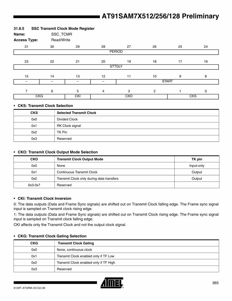
AT91SAM7X512/256/128 Preliminary
31.8.5 SSC Transmit Clock Mode Register
Name: SSC_TCMR
Access Type: Read/Write
• CKS: Transmit Clock Selection
• CKO: Transmit Clock Output Mode Selection
• CKI: Transmit Clock Inversion
0: The data outputs (Data and Frame Sync signals) are shifted out on Transmit Clock falling edge. The Frame sync signal input is sampled on Transmit clock rising edge.
1: The data outputs (Data and Frame Sync signals) are shifted out on Transmit Clock rising edge. The Frame sync signal input is sampled on Transmit clock falling edge.
CKI affects only the Transmit Clock and not the output clock signal.
• CKG: Transmit Clock Gating Selection
31 30 29 28 27 26 25 24PERIOD
23 22 21 20 19 18 17 16
STTDLY
15 14 13 12 11 10 9 8
– – – – START
7 6 5 4 3 2 1 0
CKG CKI CKO CKS
CKS Selected Transmit Clock
0x0 Divided Clock
0x1 RK Clock signal
0x2 TK Pin
0x3 Reserved
CKO Transmit Clock Output Mode TK pin
0x0 None Input-only
0x1 Continuous Transmit Clock Output
0x2 Transmit Clock only during data transfers Output
0x3-0x7 Reserved
CKG Transmit Clock Gating
0x0 None, continuous clock
0x1 Transmit Clock enabled only if TF Low
0x2 Transmit Clock enabled only if TF High
0x3 Reserved
3656120F–ATARM–03-Oct-06

AT91SAM7X512/256/128 Preliminary
• START: Transmit Start Selection
• STTDLY: Transmit Start Delay
If STTDLY is not 0, a delay of STTDLY clock cycles is inserted between the start event and the actual start of transmission of data. When the Transmitter is programmed to start synchronously with the Receiver, the delay is also applied.
Note: STTDLY must be set carefully. If STTDLY is too short in respect to TAG (Transmit Sync Data) emission, data is emit-ted instead of the end of TAG.
• PERIOD: Transmit Period Divider Selection
This field selects the divider to apply to the selected Transmit Clock to generate a new Frame Sync Signal. If 0, no period signal is generated. If not 0, a period signal is generated at each 2 x (PERIOD+1) Transmit Clock.
START Transmit Start
0x0Continuous, as soon as a word is written in the SSC_THR Register (if Transmit is enabled), and immediately after the end of transfer of the previous data.
0x1 Receive start
0x2 Detection of a low level on TF signal
0x3 Detection of a high level on TF signal
0x4 Detection of a falling edge on TF signal
0x5 Detection of a rising edge on TF signal
0x6 Detection of any level change on TF signal
0x7 Detection of any edge on TF signal
0x8 - 0xF Reserved
3666120F–ATARM–03-Oct-06

AT91SAM7X512/256/128 Preliminary
31.8.6 SSC Transmit Frame Mode Register
Name: SSC_TFMR
Access Type: Read/Write
• DATLEN: Data Length
0: Forbidden value (1-bit data length not supported).
Any other value: The bit stream contains DATLEN + 1 data bits. Moreover, it defines the transfer size performed by the PDC2 assigned to the Transmit. If DATLEN is lower or equal to 7, data transfers are bytes, if DATLEN is between 8 and 15 (included), half-words are transferred, and for any other value, 32-bit words are transferred.
• DATDEF: Data Default Value
This bit defines the level driven on the TD pin while out of transmission. Note that if the pin is defined as multi-drive by the PIO Controller, the pin is enabled only if the SCC TD output is 1.
• MSBF: Most Significant Bit First
0: The lowest significant bit of the data register is shifted out first in the bit stream.
1: The most significant bit of the data register is shifted out first in the bit stream.
• DATNB: Data Number per frame
This field defines the number of data words to be transferred after each transfer start, which is equal to (DATNB +1).
• FSLEN: Transmit Frame Sync Length
This field defines the length of the Transmit Frame Sync signal and the number of bits shifted out from the Transmit Sync Data Register if FSDEN is 1.
Pulse length is equal to (FSLEN + 1) Transmit Clock periods, i.e., the pulse length can range from 1 to 16 Transmit Clock periods. If FSLEN is 0, the Transmit Frame Sync signal is generated during one Transmit Clock period.
31 30 29 28 27 26 25 24– – – – – – – FSEDGE
23 22 21 20 19 18 17 16
FSDEN FSOS FSLEN
15 14 13 12 11 10 9 8
– – – – DATNB
7 6 5 4 3 2 1 0
MSBF – DATDEF DATLEN
3676120F–ATARM–03-Oct-06

AT91SAM7X512/256/128 Preliminary
• FSOS: Transmit Frame Sync Output Selection
• FSDEN: Frame Sync Data Enable
0: The TD line is driven with the default value during the Transmit Frame Sync signal.
1: SSC_TSHR value is shifted out during the transmission of the Transmit Frame Sync signal.
• FSEDGE: Frame Sync Edge Detection
Determines which edge on frame sync will generate the interrupt TXSYN (Status Register).
FSOS Selected Transmit Frame Sync Signal TF Pin
0x0 None Input-only
0x1 Negative Pulse Output
0x2 Positive Pulse Output
0x3 Driven Low during data transfer Output
0x4 Driven High during data transfer Output
0x5 Toggling at each start of data transfer Output
0x6-0x7 Reserved Undefined
FSEDGE Frame Sync Edge Detection
0x0 Positive Edge Detection
0x1 Negative Edge Detection
3686120F–ATARM–03-Oct-06

AT91SAM7X512/256/128 Preliminary
31.8.7 SSC Receive Holding Register
Name: SSC_RHR
Access Type: Read-only
• RDAT: Receive Data
Right aligned regardless of the number of data bits defined by DATLEN in SSC_RFMR.
31.8.8 SSC Transmit Holding Register
Name: SSC_THR
Access Type: Write-only
• TDAT: Transmit Data
Right aligned regardless of the number of data bits defined by DATLEN in SSC_TFMR.
31 30 29 28 27 26 25 24RDAT
23 22 21 20 19 18 17 16
RDAT
15 14 13 12 11 10 9 8
RDAT
7 6 5 4 3 2 1 0
RDAT
31 30 29 28 27 26 25 24
TDAT
23 22 21 20 19 18 17 16
TDAT
15 14 13 12 11 10 9 8
TDAT
7 6 5 4 3 2 1 0
TDAT
3696120F–ATARM–03-Oct-06

AT91SAM7X512/256/128 Preliminary
31.8.9 SSC Receive Synchronization Holding Register
Name: SSC_RSHR
Access Type: Read-only
• RSDAT: Receive Synchronization Data
31.8.10 SSC Transmit Synchronization Holding Register
Name: SSC_TSHR
Access Type: Read/Write
• TSDAT: Transmit Synchronization Data
31 30 29 28 27 26 25 24– – – – – – – –
23 22 21 20 19 18 17 16
– – – – – – – –
15 14 13 12 11 10 9 8
RSDAT
7 6 5 4 3 2 1 0
RSDAT
31 30 29 28 27 26 25 24
– – – – – – – –
23 22 21 20 19 18 17 16
– – – – – – – –
15 14 13 12 11 10 9 8
TSDAT
7 6 5 4 3 2 1 0
TSDAT
3706120F–ATARM–03-Oct-06
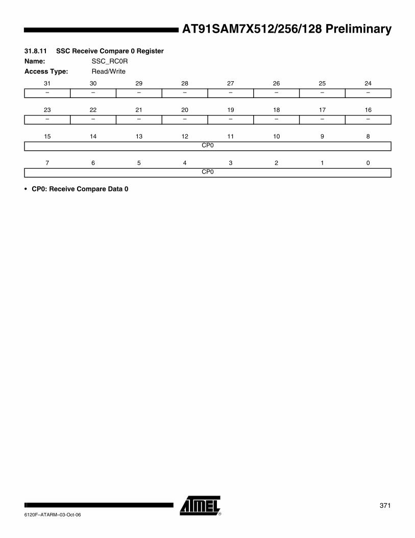
AT91SAM7X512/256/128 Preliminary
31.8.11 SSC Receive Compare 0 Register
Name: SSC_RC0R
Access Type: Read/Write
• CP0: Receive Compare Data 0
31 30 29 28 27 26 25 24– – – – – – – –
23 22 21 20 19 18 17 16
– – – – – – – –
15 14 13 12 11 10 9 8
CP0
7 6 5 4 3 2 1 0
CP0
3716120F–ATARM–03-Oct-06

AT91SAM7X512/256/128 Preliminary
31.8.12 SSC Receive Compare 1 Register
Name: SSC_RC1R
Access Type: Read/Write
• CP1: Receive Compare Data 1
31 30 29 28 27 26 25 24– – – – – – – –
23 22 21 20 19 18 17 16
– – – – – – – –
15 14 13 12 11 10 9 8
CP1
7 6 5 4 3 2 1 0
CP1
3726120F–ATARM–03-Oct-06

AT91SAM7X512/256/128 Preliminary
31.8.13 SSC Status Register
Name: SSC_SR
Access Type: Read-only
• TXRDY: Transmit Ready
0: Data has been loaded in SSC_THR and is waiting to be loaded in the Transmit Shift Register (TSR).
1: SSC_THR is empty.
• TXEMPTY: Transmit Empty
0: Data remains in SSC_THR or is currently transmitted from TSR.
1: Last data written in SSC_THR has been loaded in TSR and last data loaded in TSR has been transmitted.
• ENDTX: End of Transmission
0: The register SSC_TCR has not reached 0 since the last write in SSC_TCR or SSC_TNCR.
1: The register SSC_TCR has reached 0 since the last write in SSC_TCR or SSC_TNCR.
• TXBUFE: Transmit Buffer Empty
0: SSC_TCR or SSC_TNCR have a value other than 0.
1: Both SSC_TCR and SSC_TNCR have a value of 0.
• RXRDY: Receive Ready
0: SSC_RHR is empty.
1: Data has been received and loaded in SSC_RHR.
• OVRUN: Receive Overrun
0: No data has been loaded in SSC_RHR while previous data has not been read since the last read of the Status Register.
1: Data has been loaded in SSC_RHR while previous data has not yet been read since the last read of the Status Register.
• ENDRX: End of Reception
0: Data is written on the Receive Counter Register or Receive Next Counter Register.
1: End of PDC transfer when Receive Counter Register has arrived at zero.
• RXBUFF: Receive Buffer Full
0: SSC_RCR or SSC_RNCR have a value other than 0.
1: Both SSC_RCR and SSC_RNCR have a value of 0.
• CP0: Compare 0
0: A compare 0 has not occurred since the last read of the Status Register.
1: A compare 0 has occurred since the last read of the Status Register.
• CP1: Compare 1
0: A compare 1 has not occurred since the last read of the Status Register.
1: A compare 1 has occurred since the last read of the Status Register.
31 30 29 28 27 26 25 24– – – – – – – –
23 22 21 20 19 18 17 16
– – – – – – RXEN TXEN
15 14 13 12 11 10 9 8
– – – – RXSYN TXSYN CP1 CP0
7 6 5 4 3 2 1 0
RXBUFF ENDRX OVRUN RXRDY TXBUFE ENDTX TXEMPTY TXRDY
3736120F–ATARM–03-Oct-06

AT91SAM7X512/256/128 Preliminary
• TXSYN: Transmit Sync
0: A Tx Sync has not occurred since the last read of the Status Register.
1: A Tx Sync has occurred since the last read of the Status Register.
• RXSYN: Receive Sync
0: An Rx Sync has not occurred since the last read of the Status Register.
1: An Rx Sync has occurred since the last read of the Status Register.
• TXEN: Transmit Enable
0: Transmit is disabled.
1: Transmit is enabled.
• RXEN: Receive Enable
0: Receive is disabled.
1: Receive is enabled.
3746120F–ATARM–03-Oct-06

AT91SAM7X512/256/128 Preliminary
31.8.14 SSC Interrupt Enable Register
Name: SSC_IER
Access Type: Write-only
• TXRDY: Transmit Ready Interrupt Enable
0: No effect.
1: Enables the Transmit Ready Interrupt.
• TXEMPTY: Transmit Empty Interrupt Enable
0: No effect.
1: Enables the Transmit Empty Interrupt.
• ENDTX: End of Transmission Interrupt Enable
0: No effect.
1: Enables the End of Transmission Interrupt.
• TXBUFE: Transmit Buffer Empty Interrupt Enable
0: No effect.
1: Enables the Transmit Buffer Empty Interrupt
• RXRDY: Receive Ready Interrupt Enable
0: No effect.
1: Enables the Receive Ready Interrupt.
• OVRUN: Receive Overrun Interrupt Enable
0: No effect.
1: Enables the Receive Overrun Interrupt.
• ENDRX: End of Reception Interrupt Enable
0: No effect.
1: Enables the End of Reception Interrupt.
• RXBUFF: Receive Buffer Full Interrupt Enable
0: No effect.
1: Enables the Receive Buffer Full Interrupt.
• CP0: Compare 0 Interrupt Enable
0: No effect.
1: Enables the Compare 0 Interrupt.
• CP1: Compare 1 Interrupt Enable
0: No effect.
1: Enables the Compare 1 Interrupt.
31 30 29 28 27 26 25 24– – – – – – – –
23 22 21 20 19 18 17 16
– – – – – – – –
15 14 13 12 11 10 9 8
– – – – RXSYN TXSYN CP1 CP0
7 6 5 4 3 2 1 0
RXBUFF ENDRX OVRUN RXRDY TXBUFE ENDTX TXEMPTY TXRDY
3756120F–ATARM–03-Oct-06

AT91SAM7X512/256/128 Preliminary
• TXSYN: Tx Sync Interrupt Enable
0: No effect.
1: Enables the Tx Sync Interrupt.
• RXSYN: Rx Sync Interrupt Enable
0: No effect.
1: Enables the Rx Sync Interrupt.
3766120F–ATARM–03-Oct-06

AT91SAM7X512/256/128 Preliminary
31.8.15 SSC Interrupt Disable Register
Name: SSC_IDR
Access Type: Write-only
• TXRDY: Transmit Ready Interrupt Disable
0: No effect.
1: Disables the Transmit Ready Interrupt.
• TXEMPTY: Transmit Empty Interrupt Disable
0: No effect.
1: Disables the Transmit Empty Interrupt.
• ENDTX: End of Transmission Interrupt Disable
0: No effect.
1: Disables the End of Transmission Interrupt.
• TXBUFE: Transmit Buffer Empty Interrupt Disable
0: No effect.
1: Disables the Transmit Buffer Empty Interrupt.
• RXRDY: Receive Ready Interrupt Disable
0: No effect.
1: Disables the Receive Ready Interrupt.
• OVRUN: Receive Overrun Interrupt Disable
0: No effect.
1: Disables the Receive Overrun Interrupt.
• ENDRX: End of Reception Interrupt Disable
0: No effect.
1: Disables the End of Reception Interrupt.
• RXBUFF: Receive Buffer Full Interrupt Disable
0: No effect.
1: Disables the Receive Buffer Full Interrupt.
• CP0: Compare 0 Interrupt Disable
0: No effect.
1: Disables the Compare 0 Interrupt.
• CP1: Compare 1 Interrupt Disable
0: No effect.
1: Disables the Compare 1 Interrupt.
31 30 29 28 27 26 25 24– – – – – – – –
23 22 21 20 19 18 17 16
– – – – – – – –
15 14 13 12 11 10 9 8
– – – – RXSYN TXSYN CP1 CP0
7 6 5 4 3 2 1 0
RXBUFF ENDRX OVRUN RXRDY TXBUFE ENDTX TXEMPTY TXRDY
3776120F–ATARM–03-Oct-06
AT91SAM7X512/256/128 Preliminary
• TXSYN: Tx Sync Interrupt Enable
0: No effect.
1: Disables the Tx Sync Interrupt.
• RXSYN: Rx Sync Interrupt Enable
0: No effect.
1: Disables the Rx Sync Interrupt.
3786120F–ATARM–03-Oct-06

AT91SAM7X512/256/128 Preliminary
31.8.16 SSC Interrupt Mask Register
Name: SSC_IMR
Access Type: Read-only
• TXRDY: Transmit Ready Interrupt Mask
0: The Transmit Ready Interrupt is disabled.
1: The Transmit Ready Interrupt is enabled.
• TXEMPTY: Transmit Empty Interrupt Mask
0: The Transmit Empty Interrupt is disabled.
1: The Transmit Empty Interrupt is enabled.
• ENDTX: End of Transmission Interrupt Mask
0: The End of Transmission Interrupt is disabled.
1: The End of Transmission Interrupt is enabled.
• TXBUFE: Transmit Buffer Empty Interrupt Mask
0: The Transmit Buffer Empty Interrupt is disabled.
1: The Transmit Buffer Empty Interrupt is enabled.
• RXRDY: Receive Ready Interrupt Mask
0: The Receive Ready Interrupt is disabled.
1: The Receive Ready Interrupt is enabled.
• OVRUN: Receive Overrun Interrupt Mask
0: The Receive Overrun Interrupt is disabled.
1: The Receive Overrun Interrupt is enabled.
• ENDRX: End of Reception Interrupt Mask
0: The End of Reception Interrupt is disabled.
1: The End of Reception Interrupt is enabled.
• RXBUFF: Receive Buffer Full Interrupt Mask
0: The Receive Buffer Full Interrupt is disabled.
1: The Receive Buffer Full Interrupt is enabled.
• CP0: Compare 0 Interrupt Mask
0: The Compare 0 Interrupt is disabled.
1: The Compare 0 Interrupt is enabled.
• CP1: Compare 1 Interrupt Mask
0: The Compare 1 Interrupt is disabled.
1: The Compare 1 Interrupt is enabled.
31 30 29 28 27 26 25 24– – – – – – – –
23 22 21 20 19 18 17 16
– – – – – – – –
15 14 13 12 11 10 9 8
– – – – RXSYN TXSYN CP1 CP0
7 6 5 4 3 2 1 0
RXBUF ENDRX OVRUN RXRDY TXBUFE ENDTX TXEMPTY TXRDY
3796120F–ATARM–03-Oct-06

AT91SAM7X512/256/128 Preliminary
• TXSYN: Tx Sync Interrupt Mask
0: The Tx Sync Interrupt is disabled.
1: The Tx Sync Interrupt is enabled.
• RXSYN: Rx Sync Interrupt Mask
0: The Rx Sync Interrupt is disabled.
1: The Rx Sync Interrupt is enabled.
3806120F–ATARM–03-Oct-06

AT91SAM7X512/256/128 Preliminary
32. Timer/Counter (TC)
32.1 OverviewThe Timer Counter (TC) includes three identical 16-bit Timer Counter channels.
Each channel can be independently programmed to perform a wide range of functions including frequency measurement, event counting, interval measurement, pulse generation, delay timing and pulse width modulation.
Each channel has three external clock inputs, five internal clock inputs and two multi-purpose input/output signals which can be configured by the user. Each channel drives an internal inter-rupt signal which can be programmed to generate processor interrupts.
The Timer Counter block has two global registers which act upon all three TC channels.
The Block Control Register allows the three channels to be started simultaneously with the same instruction.
The Block Mode Register defines the external clock inputs for each channel, allowing them to be chained.
Table 32-1 gives the assignment of the device Timer Counter clock inputs common to Timer Counter 0 to 2.
Table 32-1. Timer Counter Clock Assignment
Name Definition
TIMER_CLOCK1 MCK/2
TIMER_CLOCK2 MCK/8
TIMER_CLOCK3 MCK/32
TIMER_CLOCK4 MCK/128
TIMER_CLOCK5 MCK/1024
3816120F–ATARM–03-Oct-06

32.2 Block Diagram
Figure 32-1. Timer/Counter Block Diagram
Table 32-2. Signal Name Description
Block/Channel Signal Name Description
Channel Signal
XC0, XC1, XC2 External Clock Inputs
TIOACapture Mode: Timer/Counter Input Waveform Mode: Timer/Counter Output
TIOBCapture Mode: Timer/Counter Input Waveform Mode: Timer/Counter Input/output
INT Interrupt Signal Output
SYNC Synchronization Input Signal
Timer/Counter Channel 0
Timer/Counter Channel 1
Timer/Counter Channel 2
SYNC
Parallel I/OController
TC1XC1S
TC0XC0S
TC2XC2S
INT0
INT1
INT2
TIOA0
TIOA1
TIOA2
TIOB0
TIOB1
TIOB2
XC0
XC1
XC2
XC0
XC1
XC2
XC0
XC1
XC2
TCLK0
TCLK1
TCLK2
TCLK0
TCLK1
TCLK2
TCLK0
TCLK1
TCLK2
TIOA1
TIOA2
TIOA0
TIOA2
TIOA0
TIOA1
AdvancedInterrupt
Controller
TCLK0TCLK1TCLK2
TIOA0TIOB0
TIOA1TIOB1
TIOA2TIOB2
Timer Counter
TIOA
TIOB
TIOA
TIOB
TIOA
TIOB
SYNC
SYNC
TIMER_CLOCK2
TIMER_CLOCK3
TIMER_CLOCK4
TIMER_CLOCK5
TIMER_CLOCK1
3826120F–ATARM–03-Oct-06
AT91SAM7X512/256/128 Preliminary

AT91SAM7X512/256/128 Preliminary
32.3 Pin Name List
32.4 Product Dependencies
32.4.1 I/O Lines
The pins used for interfacing the compliant external devices may be multiplexed with PIO lines. The programmer must first program the PIO controllers to assign the TC pins to their peripheral functions.
32.4.2 Power Management
The TC is clocked through the Power Management Controller (PMC), thus the programmer must first configure the PMC to enable the Timer/Counter clock.
32.4.3 Interrupt
The TC has an interrupt line connected to the Advanced Interrupt Controller (AIC). Handling the TC interrupt requires programming the AIC before configuring the TC.
Table 32-3. TC pin list
Pin Name Description Type
TCLK0-TCLK2 External Clock Input Input
TIOA0-TIOA2 I/O Line A I/O
TIOB0-TIOB2 I/O Line B I/O
3836120F–ATARM–03-Oct-06

32.5 Functional Description
32.5.1 TC Description
The three channels of the Timer/Counter are independent and identical in operation. The regis-ters for channel programming are listed in Table 32-5 on page 397.
32.5.1.1 16-bit Counter
Each channel is organized around a 16-bit counter. The value of the counter is incremented at each positive edge of the selected clock. When the counter has reached the value 0xFFFF and passes to 0x0000, an overflow occurs and the COVFS bit in TC_SR (Status Register) is set.
The current value of the counter is accessible in real time by reading the Counter Value Regis-ter, TC_CV. The counter can be reset by a trigger. In this case, the counter value passes to 0x0000 on the next valid edge of the selected clock.
32.5.1.2 Clock Selection
At block level, input clock signals of each channel can either be connected to the external inputs TCLK0, TCLK1 or TCLK2, or be connected to the configurable I/O signals TIOA0, TIOA1 or TIOA2 for chaining by programming the TC_BMR (Block Mode). See Figure 32-2.
Each channel can independently select an internal or external clock source for its counter:
• Internal clock signals: TIMER_CLOCK1, TIMER_CLOCK2, TIMER_CLOCK3, TIMER_CLOCK4, TIMER_CLOCK5
• External clock signals: XC0, XC1 or XC2
This selection is made by the TCCLKS bits in the TC Channel Mode Register.
The selected clock can be inverted with the CLKI bit in TC_CMR. This allows counting on the opposite edges of the clock.
The burst function allows the clock to be validated when an external signal is high. The BURST parameter in the Mode Register defines this signal (none, XC0, XC1, XC2).
Note: In all cases, if an external clock is used, the duration of each of its levels must be longer than the master clock period. The external clock frequency must be at least 2.5 times lower than the mas-ter clock
3846120F–ATARM–03-Oct-06
AT91SAM7X512/256/128 Preliminary

AT91SAM7X512/256/128 Preliminary
Figure 32-2. Clock Selection
32.5.1.3 Clock Control
The clock of each counter can be controlled in two different ways: it can be enabled/disabled and started/stopped. See Figure 32-3.
• The clock can be enabled or disabled by the user with the CLKEN and the CLKDIS commands in the Control Register. In Capture Mode it can be disabled by an RB load event if LDBDIS is set to 1 in TC_CMR. In Waveform Mode, it can be disabled by an RC Compare event if CPCDIS is set to 1 in TC_CMR. When disabled, the start or the stop actions have no effect: only a CLKEN command in the Control Register can re-enable the clock. When the clock is enabled, the CLKSTA bit is set in the Status Register.
• The clock can also be started or stopped: a trigger (software, synchro, external or compare) always starts the clock. The clock can be stopped by an RB load event in Capture Mode (LDBSTOP = 1 in TC_CMR) or a RC compare event in Waveform Mode (CPCSTOP = 1 in TC_CMR). The start and the stop commands have effect only if the clock is enabled.
TIMER_CLOCK1
TIMER_CLOCK2
TIMER_CLOCK3
TIMER_CLOCK4
TIMER_CLOCK5
XC0
XC1
XC2
TCCLKS
CLKI
BURST
1
SelectedClock
3856120F–ATARM–03-Oct-06
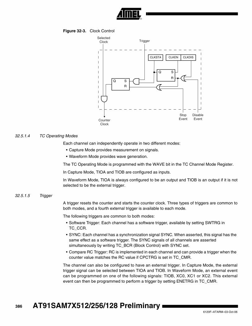
Figure 32-3. Clock Control
32.5.1.4 TC Operating Modes
Each channel can independently operate in two different modes:
• Capture Mode provides measurement on signals.
• Waveform Mode provides wave generation.
The TC Operating Mode is programmed with the WAVE bit in the TC Channel Mode Register.
In Capture Mode, TIOA and TIOB are configured as inputs.
In Waveform Mode, TIOA is always configured to be an output and TIOB is an output if it is not selected to be the external trigger.
32.5.1.5 Trigger
A trigger resets the counter and starts the counter clock. Three types of triggers are common to both modes, and a fourth external trigger is available to each mode.
The following triggers are common to both modes:
• Software Trigger: Each channel has a software trigger, available by setting SWTRG in TC_CCR.
• SYNC: Each channel has a synchronization signal SYNC. When asserted, this signal has the same effect as a software trigger. The SYNC signals of all channels are asserted simultaneously by writing TC_BCR (Block Control) with SYNC set.
• Compare RC Trigger: RC is implemented in each channel and can provide a trigger when the counter value matches the RC value if CPCTRG is set in TC_CMR.
The channel can also be configured to have an external trigger. In Capture Mode, the external trigger signal can be selected between TIOA and TIOB. In Waveform Mode, an external event can be programmed on one of the following signals: TIOB, XC0, XC1 or XC2. This external event can then be programmed to perform a trigger by setting ENETRG in TC_CMR.
Q S
R
S
R
Q
CLKSTA CLKEN CLKDIS
StopEvent
DisableEventCounter
Clock
SelectedClock Trigger
3866120F–ATARM–03-Oct-06
AT91SAM7X512/256/128 Preliminary
AT91SAM7X512/256/128 Preliminary
If an external trigger is used, the duration of the pulses must be longer than the master clock period in order to be detected.
Regardless of the trigger used, it will be taken into account at the following active edge of the selected clock. This means that the counter value can be read differently from zero just after a trigger, especially when a low frequency signal is selected as the clock.
32.5.2 Capture Operating Mode
This mode is entered by clearing the WAVE parameter in TC_CMR (Channel Mode Register).
Capture Mode allows the TC channel to perform measurements such as pulse timing, fre-quency, period, duty cycle and phase on TIOA and TIOB signals which are considered as inputs.
Figure 32-4 shows the configuration of the TC channel when programmed in Capture Mode.
32.5.2.1 Capture Registers A and B
Registers A and B (RA and RB) are used as capture registers. This means that they can be loaded with the counter value when a programmable event occurs on the signal TIOA.
The LDRA parameter in TC_CMR defines the TIOA edge for the loading of register A, and the LDRB parameter defines the TIOA edge for the loading of Register B.
RA is loaded only if it has not been loaded since the last trigger or if RB has been loaded since the last loading of RA.
RB is loaded only if RA has been loaded since the last trigger or the last loading of RB.
Loading RA or RB before the read of the last value loaded sets the Overrun Error Flag (LOVRS) in TC_SR (Status Register). In this case, the old value is overwritten.
32.5.2.2 Trigger Conditions
In addition to the SYNC signal, the software trigger and the RC compare trigger, an external trig-ger can be defined.
The ABETRG bit in TC_CMR selects TIOA or TIOB input signal as an external trigger. The ETRGEDG parameter defines the edge (rising, falling or both) detected to generate an external trigger. If ETRGEDG = 0 (none), the external trigger is disabled.
3876120F–ATARM–03-Oct-06

Figure 32-4. Capture Mode
TIM
ER
_CLO
CK
1
TIM
ER
_CLO
CK
2
TIM
ER
_CLO
CK
3
TIM
ER
_CLO
CK
4
TIM
ER
_CLO
CK
5
XC
0
XC
1
XC
2
TC
CLK
S
CLK
I
QS R
S R
Q
CLK
ST
AC
LKE
NC
LKD
IS
BU
RS
T
TIO
B
Reg
iste
r C
Cap
ture
R
egis
ter
A
Cap
ture
R
egis
ter
BC
ompa
re R
C =
16-b
it C
ount
er
AB
ET
RG
SW
TR
G
ET
RG
ED
GC
PC
TR
G
TC1_IMR
Trig
LDRBS
LDRAS
ETRGS
TC1_SR
LOVRS
COVFS
SY
NC
1
MT
IOB
TIO
A
MT
IOA
LDR
A
LDB
ST
OP
If R
A is
not
load
edor
RB
is L
oade
dIf
RA
is L
oade
d
LDB
DIS
CPCS
INT
Edg
eD
etec
tor
Edg
e D
etec
tor
LDR
B
Edg
e D
etec
tor
CLK
OV
F
RE
SE
T
Tim
er/C
ount
er C
hann
el
3886120F–ATARM–03-Oct-06
AT91SAM7X512/256/128 Preliminary

AT91SAM7X512/256/128 Preliminary
32.5.3 Waveform Operating Mode
Waveform operating mode is entered by setting the WAVE parameter in TC_CMR (Channel Mode Register).
In Waveform Operating Mode the TC channel generates 1 or 2 PWM signals with the same fre-quency and independently programmable duty cycles, or generates different types of one-shot or repetitive pulses.
In this mode, TIOA is configured as an output and TIOB is defined as an output if it is not used as an external event (EEVT parameter in TC_CMR).
Figure 32-5 shows the configuration of the TC channel when programmed in Waveform Operat-ing Mode.
32.5.3.1 Waveform Selection
Depending on the WAVSEL parameter in TC_CMR (Channel Mode Register), the behavior of TC_CV varies.
With any selection, RA, RB and RC can all be used as compare registers.
RA Compare is used to control the TIOA output, RB Compare is used to control the TIOB output (if correctly configured) and RC Compare is used to control TIOA and/or TIOB outputs.
3896120F–ATARM–03-Oct-06

Figure 32-5. Waveform Mode
TC
CLK
S
CLK
I
QS R
S R
Q
CLK
ST
AC
LKE
NC
LKD
IS
CP
CD
IS
BU
RS
T
TIO
B
Reg
iste
r A
Reg
iste
r B
Reg
iste
r C
Com
pare
RA
=
Com
pare
RB
=
Com
pare
RC
=
CP
CS
TO
P
16-b
it C
ount
er
EE
VT
EE
VT
ED
G
SY
NC
SW
TR
G
EN
ET
RG
WA
VS
EL
TC1_IMRT
rig
AC
PC
AC
PA
AE
EV
T
AS
WT
RG
BC
PC
BC
PB
BE
EV
T
BS
WT
RG
TIO
A
MT
IOA
TIO
B
MT
IOB
CPAS
COVFS
ETRGS
TC1_SR
CPCS
CPBSC
LKO
VF
RE
SE
T
Output Controller Output Controller
INT
1
Edg
e D
etec
tor
Tim
er/C
ount
er C
hann
el
TIM
ER
_CLO
CK
1
TIM
ER
_CLO
CK
2
TIM
ER
_CLO
CK
3
TIM
ER
_CLO
CK
4
TIM
ER
_CLO
CK
5
XC
0
XC
1
XC
2
WA
VS
EL
3906120F–ATARM–03-Oct-06
AT91SAM7X512/256/128 Preliminary
AT91SAM7X512/256/128 Preliminary
32.5.3.2 WAVSEL = 00
When WAVSEL = 00, the value of TC_CV is incremented from 0 to 0xFFFF. Once 0xFFFF has been reached, the value of TC_CV is reset. Incrementation of TC_CV starts again and the cycle continues. See Figure 32-6.
An external event trigger or a software trigger can reset the value of TC_CV. It is important to note that the trigger may occur at any time. See Figure 32-7.
RC Compare cannot be programmed to generate a trigger in this configuration. At the same time, RC Compare can stop the counter clock (CPCSTOP = 1 in TC_CMR) and/or disable the counter clock (CPCDIS = 1 in TC_CMR).
Figure 32-6. WAVSEL= 00 without trigger
Time
Counter Value
RC
RB
RA
TIOB
TIOA
Counter cleared by compare match with 0xFFFF
0xFFFF
Waveform Examples
3916120F–ATARM–03-Oct-06
Figure 32-7. WAVSEL= 00 with trigger
32.5.3.3 WAVSEL = 10
When WAVSEL = 10, the value of TC_CV is incremented from 0 to the value of RC, then auto-matically reset on a RC Compare. Once the value of TC_CV has been reset, it is then incremented and so on. See Figure 32-8.
It is important to note that TC_CV can be reset at any time by an external event or a software trigger if both are programmed correctly. See Figure 32-9.
In addition, RC Compare can stop the counter clock (CPCSTOP = 1 in TC_CMR) and/or disable the counter clock (CPCDIS = 1 in TC_CMR).
Time
Counter Value
RC
RB
RA
TIOB
TIOA
Counter cleared by compare match with 0xFFFF
0xFFFF
Waveform Examples
Counter cleared by trigger
3926120F–ATARM–03-Oct-06
AT91SAM7X512/256/128 Preliminary

AT91SAM7X512/256/128 Preliminary
Figure 32-8. WAVSEL = 10 Without Trigger
Figure 32-9. WAVSEL = 10 With Trigger
32.5.3.4 WAVSEL = 01
When WAVSEL = 01, the value of TC_CV is incremented from 0 to 0xFFFF. Once 0xFFFF is reached, the value of TC_CV is decremented to 0, then re-incremented to 0xFFFF and so on. See Figure 32-10.
A trigger such as an external event or a software trigger can modify TC_CV at any time. If a trig-ger occurs while TC_CV is incrementing, TC_CV then decrements. If a trigger is received while TC_CV is decrementing, TC_CV then increments. See Figure 32-11.
Time
Counter Value
RC
RB
RA
TIOB
TIOA
Counter cleared by compare match with RC0xFFFF
Waveform Examples
Time
Counter Value
RC
RB
RA
TIOB
TIOA
Counter cleared by compare match with RC0xFFFF
Waveform Examples
Counter cleared by trigger
3936120F–ATARM–03-Oct-06
RC Compare cannot be programmed to generate a trigger in this configuration.
At the same time, RC Compare can stop the counter clock (CPCSTOP = 1) and/or disable the counter clock (CPCDIS = 1).
Figure 32-10. WAVSEL = 01 Without Trigger
Figure 32-11. WAVSEL = 01 With Trigger
32.5.3.5 WAVSEL = 11
When WAVSEL = 11, the value of TC_CV is incremented from 0 to RC. Once RC is reached, the value of TC_CV is decremented to 0, then re-incremented to RC and so on. See Figure 32-12.
Time
Counter Value
RC
RB
RA
TIOB
TIOA
Counter decremented by compare match with 0xFFFF
0xFFFF
Waveform Examples
Time
Counter Value
TIOB
TIOA
Counter decremented by compare match with 0xFFFF
0xFFFF
Waveform Examples
Counter decremented by trigger
Counter incremented by trigger
RC
RB
RA
3946120F–ATARM–03-Oct-06
AT91SAM7X512/256/128 Preliminary
AT91SAM7X512/256/128 Preliminary
A trigger such as an external event or a software trigger can modify TC_CV at any time. If a trig-ger occurs while TC_CV is incrementing, TC_CV then decrements. If a trigger is received while TC_CV is decrementing, TC_CV then increments. See Figure 32-13.
RC Compare can stop the counter clock (CPCSTOP = 1) and/or disable the counter clock (CPC-DIS = 1).
Figure 32-12. WAVSEL = 11 Without Trigger
Figure 32-13. WAVSEL = 11 With Trigger
32.5.3.6 External Event/Trigger ConditionsAn external event can be programmed to be detected on one of the clock sources (XC0, XC1, XC2) or TIOB. The external event selected can then be used as a trigger.
Time
Counter Value
RC
RB
RA
TIOB
TIOA
Counter decremented by compare match with RC
0xFFFF
Waveform Examples
Time
Counter Value
TIOB
TIOA
Counter decremented by compare match with RC
0xFFFF
Waveform Examples
Counter decremented by trigger
Counter incremented by trigger
RC
RB
RA
3956120F–ATARM–03-Oct-06

The EEVT parameter in TC_CMR selects the external trigger. The EEVTEDG parameter defines the trigger edge for each of the possible external triggers (rising, falling or both). If EEVTEDG is cleared (none), no external event is defined.
If TIOB is defined as an external event signal (EEVT = 0), TIOB is no longer used as an output and the compare register B is not used to generate waveforms and subsequently no IRQs. In this case the TC channel can only generate a waveform on TIOA.
When an external event is defined, it can be used as a trigger by setting bit ENETRG in TC_CMR.
As in Capture Mode, the SYNC signal and the software trigger are also available as triggers. RC Compare can also be used as a trigger depending on the parameter WAVSEL.
32.5.3.7 Output Controller
The output controller defines the output level changes on TIOA and TIOB following an event. TIOB control is used only if TIOB is defined as output (not as an external event).
The following events control TIOA and TIOB: software trigger, external event and RC compare. RA compare controls TIOA and RB compare controls TIOB. Each of these events can be pro-grammed to set, clear or toggle the output as defined in the corresponding parameter in TC_CMR.
3966120F–ATARM–03-Oct-06
AT91SAM7X512/256/128 Preliminary

AT91SAM7X512/256/128 Preliminary
32.6 Timer/Counter (TC) User Interface
32.6.1 Global Register Mapping
TC_BCR (Block Control Register) and TC_BMR (Block Mode Register) control the whole TC block. TC channels are controlled by the registers listed in Table 32-5. The offset of each of the channel registers in Table 32-5 is in relation to the offset of the corresponding channel as men-tioned in Table 32-5.
32.6.2 Channel Memory Mapping
Notes: 1. Read-only if WAVE = 0
Table 32-4. Timer/Counter (TC) Global Register Map
Offset Channel/Register Name Access Reset Value
0x00 TC Channel 0 See Table 32-5
0x40 TC Channel 1 See Table 32-5
0x80 TC Channel 2 See Table 32-5
0xC0 TC Block Control Register TC_BCR Write-only –
0xC4 TC Block Mode Register TC_BMR Read/Write 0
Table 32-5. TC Channel Memory Map
Offset Register Name Access Reset Value
0x00 Channel Control Register TC_CCR Write-only –
0x04 Channel Mode Register TC_CMR Read/Write 0
0x08 Reserved –
0x0C Reserved –
0x10 Counter Value TC_CV Read-only 0
0x14 Register A TC_RA Read/Write(1) 0
0x18 Register B TC_RB Read/Write(1) 0
0x1C Register C TC_RC Read/Write 0
0x20 Status Register TC_SR Read-only 0
0x24 Interrupt Enable Register TC_IER Write-only –
0x28 Interrupt Disable Register TC_IDR Write-only –
0x2C Interrupt Mask Register TC_IMR Read-only 0
0xFC Reserved – – –
3976120F–ATARM–03-Oct-06

32.6.3 TC Block Control Register
Register Name: TC_BCR
Access Type: Write-only
• SYNC: Synchro Command
0 = No effect.
1 = Asserts the SYNC signal which generates a software trigger simultaneously for each of the channels.
31 30 29 28 27 26 25 24
– – – – – – – –
23 22 21 20 19 18 17 16
– – – – – – – –
15 14 13 12 11 10 9 8
– – – – – – – –
7 6 5 4 3 2 1 0
– – – – – – – SYNC
3986120F–ATARM–03-Oct-06
AT91SAM7X512/256/128 Preliminary

AT91SAM7X512/256/128 Preliminary
32.6.4 TC Block Mode Register
Register Name: TC_BMR
Access Type: Read/Write
• TC0XC0S: External Clock Signal 0 Selection
• TC1XC1S: External Clock Signal 1 Selection
• TC2XC2S: External Clock Signal 2 Selection
31 30 29 28 27 26 25 24
– – – – – – – –
23 22 21 20 19 18 17 16
– – – – – – – –
15 14 13 12 11 10 9 8
– – – – – – – –
7 6 5 4 3 2 1 0
– – TC2XC2S TCXC1S TC0XC0S
TC0XC0S Signal Connected to XC0
0 0 TCLK0
0 1 none
1 0 TIOA1
1 1 TIOA2
TC1XC1S Signal Connected to XC1
0 0 TCLK1
0 1 none
1 0 TIOA0
1 1 TIOA2
TC2XC2S Signal Connected to XC2
0 0 TCLK2
0 1 none
1 0 TIOA0
1 1 TIOA1
3996120F–ATARM–03-Oct-06

32.6.5 TC Channel Control Register
Register Name: TC_CCR
Access Type: Write-only
• CLKEN: Counter Clock Enable Command
0 = No effect.
1 = Enables the clock if CLKDIS is not 1.
• CLKDIS: Counter Clock Disable Command
0 = No effect.
1 = Disables the clock.
• SWTRG: Software Trigger Command
0 = No effect.
1 = A software trigger is performed: the counter is reset and the clock is started.
31 30 29 28 27 26 25 24
– – – – – – – –
23 22 21 20 19 18 17 16
– – – – – – – –
15 14 13 12 11 10 9 8
– – – – – – – –
7 6 5 4 3 2 1 0
– – – – – SWTRG CLKDIS CLKEN
4006120F–ATARM–03-Oct-06
AT91SAM7X512/256/128 Preliminary

AT91SAM7X512/256/128 Preliminary
32.6.6 TC Channel Mode Register: Capture Mode
Register Name: TC_CMR
Access Type: Read/Write
• TCCLKS: Clock Selection
• CLKI: Clock Invert
0 = Counter is incremented on rising edge of the clock.
1 = Counter is incremented on falling edge of the clock.
• BURST: Burst Signal Selection
• LDBSTOP: Counter Clock Stopped with RB Loading
0 = Counter clock is not stopped when RB loading occurs.
1 = Counter clock is stopped when RB loading occurs.
• LDBDIS: Counter Clock Disable with RB Loading
0 = Counter clock is not disabled when RB loading occurs.
1 = Counter clock is disabled when RB loading occurs.
31 30 29 28 27 26 25 24
– – – – – – – –
23 22 21 20 19 18 17 16
– – – – LDRB LDRA
15 14 13 12 11 10 9 8
WAVE = 0 CPCTRG – – – ABETRG ETRGEDG
7 6 5 4 3 2 1 0
LDBDIS LDBSTOP BURST CLKI TCCLKS
TCCLKS Clock Selected
0 0 0 TIMER_CLOCK1
0 0 1 TIMER_CLOCK2
0 1 0 TIMER_CLOCK3
0 1 1 TIMER_CLOCK4
1 0 0 TIMER_CLOCK5
1 0 1 XC0
1 1 0 XC1
1 1 1 XC2
BURST
0 0 The clock is not gated by an external signal.
0 1 XC0 is ANDed with the selected clock.
1 0 XC1 is ANDed with the selected clock.
1 1 XC2 is ANDed with the selected clock.
4016120F–ATARM–03-Oct-06
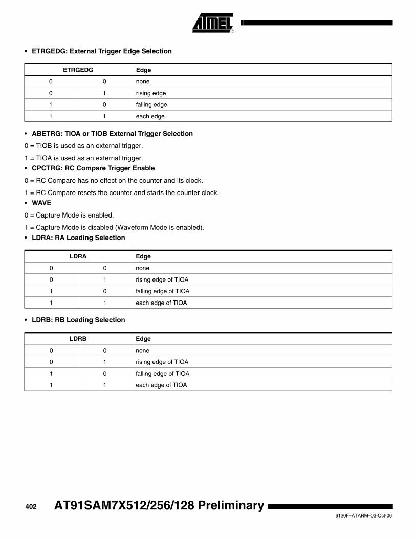
• ETRGEDG: External Trigger Edge Selection
• ABETRG: TIOA or TIOB External Trigger Selection
0 = TIOB is used as an external trigger.
1 = TIOA is used as an external trigger.
• CPCTRG: RC Compare Trigger Enable
0 = RC Compare has no effect on the counter and its clock.
1 = RC Compare resets the counter and starts the counter clock.
• WAVE
0 = Capture Mode is enabled.
1 = Capture Mode is disabled (Waveform Mode is enabled).
• LDRA: RA Loading Selection
• LDRB: RB Loading Selection
ETRGEDG Edge
0 0 none
0 1 rising edge
1 0 falling edge
1 1 each edge
LDRA Edge
0 0 none
0 1 rising edge of TIOA
1 0 falling edge of TIOA
1 1 each edge of TIOA
LDRB Edge
0 0 none
0 1 rising edge of TIOA
1 0 falling edge of TIOA
1 1 each edge of TIOA
4026120F–ATARM–03-Oct-06
AT91SAM7X512/256/128 Preliminary
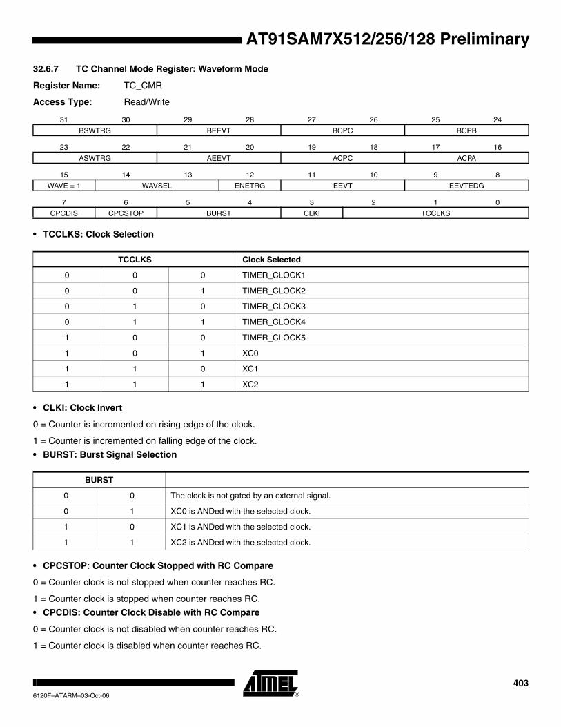
AT91SAM7X512/256/128 Preliminary
32.6.7 TC Channel Mode Register: Waveform Mode
Register Name: TC_CMR
Access Type: Read/Write
• TCCLKS: Clock Selection
• CLKI: Clock Invert
0 = Counter is incremented on rising edge of the clock.
1 = Counter is incremented on falling edge of the clock.
• BURST: Burst Signal Selection
• CPCSTOP: Counter Clock Stopped with RC Compare
0 = Counter clock is not stopped when counter reaches RC.
1 = Counter clock is stopped when counter reaches RC.
• CPCDIS: Counter Clock Disable with RC Compare
0 = Counter clock is not disabled when counter reaches RC.
1 = Counter clock is disabled when counter reaches RC.
31 30 29 28 27 26 25 24
BSWTRG BEEVT BCPC BCPB
23 22 21 20 19 18 17 16
ASWTRG AEEVT ACPC ACPA
15 14 13 12 11 10 9 8
WAVE = 1 WAVSEL ENETRG EEVT EEVTEDG
7 6 5 4 3 2 1 0
CPCDIS CPCSTOP BURST CLKI TCCLKS
TCCLKS Clock Selected
0 0 0 TIMER_CLOCK1
0 0 1 TIMER_CLOCK2
0 1 0 TIMER_CLOCK3
0 1 1 TIMER_CLOCK4
1 0 0 TIMER_CLOCK5
1 0 1 XC0
1 1 0 XC1
1 1 1 XC2
BURST
0 0 The clock is not gated by an external signal.
0 1 XC0 is ANDed with the selected clock.
1 0 XC1 is ANDed with the selected clock.
1 1 XC2 is ANDed with the selected clock.
4036120F–ATARM–03-Oct-06

• EEVTEDG: External Event Edge Selection
• EEVT: External Event Selection
Note: 1. If TIOB is chosen as the external event signal, it is configured as an input and no longer generates waveforms and sub-sequently no IRQs.
• ENETRG: External Event Trigger Enable
0 = The external event has no effect on the counter and its clock. In this case, the selected external event only controls the TIOA output.
1 = The external event resets the counter and starts the counter clock.
• WAVSEL: Waveform Selection
• WAVE = 1
0 = Waveform Mode is disabled (Capture Mode is enabled).
1 = Waveform Mode is enabled.
• ACPA: RA Compare Effect on TIOA
EEVTEDG Edge
0 0 none
0 1 rising edge
1 0 falling edge
1 1 each edge
EEVT Signal selected as external event TIOB Direction
0 0 TIOB input(1)
0 1 XC0 output
1 0 XC1 output
1 1 XC2 output
WAVSEL Effect
0 0 UP mode without automatic trigger on RC Compare
1 0 UP mode with automatic trigger on RC Compare
0 1 UPDOWN mode without automatic trigger on RC Compare
1 1 UPDOWN mode with automatic trigger on RC Compare
ACPA Effect
0 0 none
0 1 set
1 0 clear
1 1 toggle
4046120F–ATARM–03-Oct-06
AT91SAM7X512/256/128 Preliminary

AT91SAM7X512/256/128 Preliminary
• ACPC: RC Compare Effect on TIOA
• AEEVT: External Event Effect on TIOA
• ASWTRG: Software Trigger Effect on TIOA
• BCPB: RB Compare Effect on TIOB
• BCPC: RC Compare Effect on TIOB
ACPC Effect
0 0 none
0 1 set
1 0 clear
1 1 toggle
AEEVT Effect
0 0 none
0 1 set
1 0 clear
1 1 toggle
ASWTRG Effect
0 0 none
0 1 set
1 0 clear
1 1 toggle
BCPB Effect
0 0 none
0 1 set
1 0 clear
1 1 toggle
BCPC Effect
0 0 none
0 1 set
1 0 clear
1 1 toggle
4056120F–ATARM–03-Oct-06
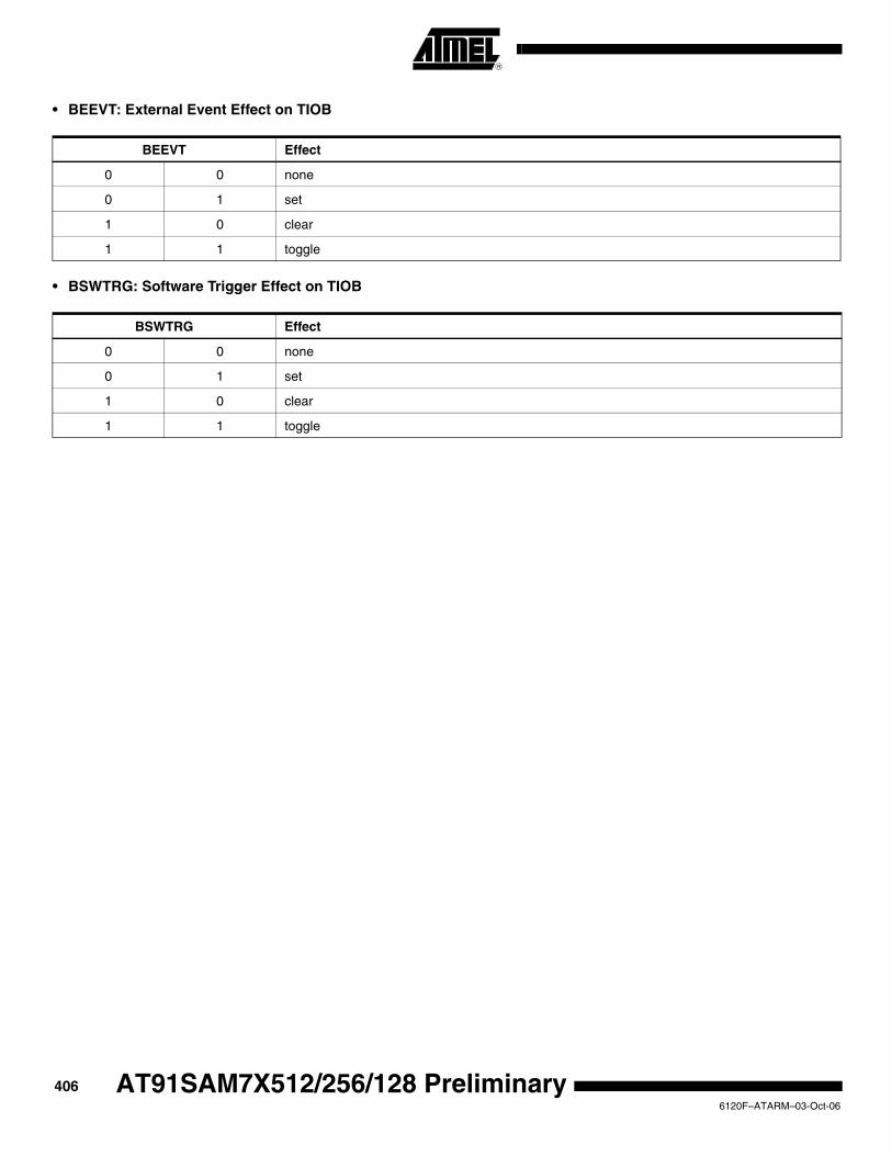
• BEEVT: External Event Effect on TIOB
• BSWTRG: Software Trigger Effect on TIOB
BEEVT Effect
0 0 none
0 1 set
1 0 clear
1 1 toggle
BSWTRG Effect
0 0 none
0 1 set
1 0 clear
1 1 toggle
4066120F–ATARM–03-Oct-06
AT91SAM7X512/256/128 Preliminary

AT91SAM7X512/256/128 Preliminary
32.6.8 TC Counter Value Register
Register Name: TC_CV
Access Type: Read-only
• CV: Counter Value
CV contains the counter value in real time.
31 30 29 28 27 26 25 24
– – – – – – – –
23 22 21 20 19 18 17 16
– – – – – – – –
15 14 13 12 11 10 9 8
CV
7 6 5 4 3 2 1 0
CV
4076120F–ATARM–03-Oct-06
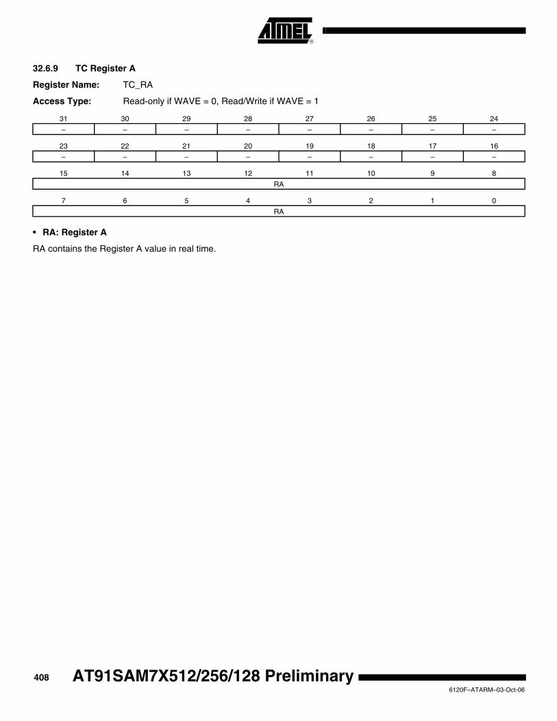
32.6.9 TC Register A
Register Name: TC_RA
Access Type: Read-only if WAVE = 0, Read/Write if WAVE = 1
• RA: Register A
RA contains the Register A value in real time.
31 30 29 28 27 26 25 24
– – – – – – – –
23 22 21 20 19 18 17 16
– – – – – – – –
15 14 13 12 11 10 9 8
RA
7 6 5 4 3 2 1 0
RA
4086120F–ATARM–03-Oct-06
AT91SAM7X512/256/128 Preliminary

AT91SAM7X512/256/128 Preliminary
32.6.10 TC Register B
Register Name: TC_RB
Access Type: Read-only if WAVE = 0, Read/Write if WAVE = 1
• RB: Register B
RB contains the Register B value in real time.
32.6.11 TC Register C
Register Name: TC_RC
Access Type: Read/Write
• RC: Register C
RC contains the Register C value in real time.
31 30 29 28 27 26 25 24
– – – – – – – –
23 22 21 20 19 18 17 16
– – – – – – – –
15 14 13 12 11 10 9 8
RB
7 6 5 4 3 2 1 0
RB
31 30 29 28 27 26 25 24
– – – – – – – –
23 22 21 20 19 18 17 16
– – – – – – – –
15 14 13 12 11 10 9 8
RC
7 6 5 4 3 2 1 0
RC
4096120F–ATARM–03-Oct-06

32.6.12 TC Status Register
Register Name: TC_SR
Access Type: Read-only
• COVFS: Counter Overflow Status
0 = No counter overflow has occurred since the last read of the Status Register.
1 = A counter overflow has occurred since the last read of the Status Register.
• LOVRS: Load Overrun Status
0 = Load overrun has not occurred since the last read of the Status Register or WAVE = 1.
1 = RA or RB have been loaded at least twice without any read of the corresponding register since the last read of the Sta-tus Register, if WAVE = 0.
• CPAS: RA Compare Status
0 = RA Compare has not occurred since the last read of the Status Register or WAVE = 0.
1 = RA Compare has occurred since the last read of the Status Register, if WAVE = 1.
• CPBS: RB Compare Status
0 = RB Compare has not occurred since the last read of the Status Register or WAVE = 0.
1 = RB Compare has occurred since the last read of the Status Register, if WAVE = 1.
• CPCS: RC Compare Status
0 = RC Compare has not occurred since the last read of the Status Register.
1 = RC Compare has occurred since the last read of the Status Register.
• LDRAS: RA Loading Status
0 = RA Load has not occurred since the last read of the Status Register or WAVE = 1.
1 = RA Load has occurred since the last read of the Status Register, if WAVE = 0.
• LDRBS: RB Loading Status
0 = RB Load has not occurred since the last read of the Status Register or WAVE = 1.
1 = RB Load has occurred since the last read of the Status Register, if WAVE = 0.
• ETRGS: External Trigger Status
0 = External trigger has not occurred since the last read of the Status Register.
1 = External trigger has occurred since the last read of the Status Register.
• CLKSTA: Clock Enabling Status
0 = Clock is disabled.
1 = Clock is enabled.
31 30 29 28 27 26 25 24
– – – – – – – –
23 22 21 20 19 18 17 16
– – – – – MTIOB MTIOA CLKSTA
15 14 13 12 11 10 9 8
– – – – – – – –
7 6 5 4 3 2 1 0
ETRGS LDRBS LDRAS CPCS CPBS CPAS LOVRS COVFS
4106120F–ATARM–03-Oct-06
AT91SAM7X512/256/128 Preliminary
AT91SAM7X512/256/128 Preliminary
• MTIOA: TIOA Mirror
0 = TIOA is low. If WAVE = 0, this means that TIOA pin is low. If WAVE = 1, this means that TIOA is driven low.
1 = TIOA is high. If WAVE = 0, this means that TIOA pin is high. If WAVE = 1, this means that TIOA is driven high.
• MTIOB: TIOB Mirror
0 = TIOB is low. If WAVE = 0, this means that TIOB pin is low. If WAVE = 1, this means that TIOB is driven low.
1 = TIOB is high. If WAVE = 0, this means that TIOB pin is high. If WAVE = 1, this means that TIOB is driven high.
4116120F–ATARM–03-Oct-06

32.6.13 TC Interrupt Enable Register
Register Name: TC_IER
Access Type: Write-only
• COVFS: Counter Overflow
0 = No effect.
1 = Enables the Counter Overflow Interrupt.
• LOVRS: Load Overrun
0 = No effect.
1 = Enables the Load Overrun Interrupt.
• CPAS: RA Compare
0 = No effect.
1 = Enables the RA Compare Interrupt.
• CPBS: RB Compare
0 = No effect.
1 = Enables the RB Compare Interrupt.
• CPCS: RC Compare
0 = No effect.
1 = Enables the RC Compare Interrupt.
• LDRAS: RA Loading
0 = No effect.
1 = Enables the RA Load Interrupt.
• LDRBS: RB Loading
0 = No effect.
1 = Enables the RB Load Interrupt.
• ETRGS: External Trigger
0 = No effect.
1 = Enables the External Trigger Interrupt.
31 30 29 28 27 26 25 24
– – – – – – – –
23 22 21 20 19 18 17 16
– – – – – – – –
15 14 13 12 11 10 9 8
– – – – – – – –
7 6 5 4 3 2 1 0
ETRGS LDRBS LDRAS CPCS CPBS CPAS LOVRS COVFS
4126120F–ATARM–03-Oct-06
AT91SAM7X512/256/128 Preliminary

AT91SAM7X512/256/128 Preliminary
32.6.14 TC Interrupt Disable Register
Register Name: TC_IDR
Access Type: Write-only
• COVFS: Counter Overflow
0 = No effect.
1 = Disables the Counter Overflow Interrupt.
• LOVRS: Load Overrun
0 = No effect.
1 = Disables the Load Overrun Interrupt (if WAVE = 0).
• CPAS: RA Compare
0 = No effect.
1 = Disables the RA Compare Interrupt (if WAVE = 1).
• CPBS: RB Compare
0 = No effect.
1 = Disables the RB Compare Interrupt (if WAVE = 1).
• CPCS: RC Compare
0 = No effect.
1 = Disables the RC Compare Interrupt.
• LDRAS: RA Loading
0 = No effect.
1 = Disables the RA Load Interrupt (if WAVE = 0).
• LDRBS: RB Loading
0 = No effect.
1 = Disables the RB Load Interrupt (if WAVE = 0).
• ETRGS: External Trigger
0 = No effect.
1 = Disables the External Trigger Interrupt.
31 30 29 28 27 26 25 24
– – – – – – – –
23 22 21 20 19 18 17 16
– – – – – – – –
15 14 13 12 11 10 9 8
– – – – – – – –
7 6 5 4 3 2 1 0
ETRGS LDRBS LDRAS CPCS CPBS CPAS LOVRS COVFS
4136120F–ATARM–03-Oct-06

32.6.15 TC Interrupt Mask Register
Register Name: TC_IMR
Access Type: Read-only
• COVFS: Counter Overflow
0 = The Counter Overflow Interrupt is disabled.
1 = The Counter Overflow Interrupt is enabled.
• LOVRS: Load Overrun
0 = The Load Overrun Interrupt is disabled.
1 = The Load Overrun Interrupt is enabled.
• CPAS: RA Compare
0 = The RA Compare Interrupt is disabled.
1 = The RA Compare Interrupt is enabled.
• CPBS: RB Compare
0 = The RB Compare Interrupt is disabled.
1 = The RB Compare Interrupt is enabled.
• CPCS: RC Compare
0 = The RC Compare Interrupt is disabled.
1 = The RC Compare Interrupt is enabled.
• LDRAS: RA Loading
0 = The Load RA Interrupt is disabled.
1 = The Load RA Interrupt is enabled.
• LDRBS: RB Loading
0 = The Load RB Interrupt is disabled.
1 = The Load RB Interrupt is enabled.
• ETRGS: External Trigger
0 = The External Trigger Interrupt is disabled.
1 = The External Trigger Interrupt is enabled.
31 30 29 28 27 26 25 24
– – – – – – – –
23 22 21 20 19 18 17 16
– – – – – – – –
15 14 13 12 11 10 9 8
– – – – – – – –
7 6 5 4 3 2 1 0
ETRGS LDRBS LDRAS CPCS CPBS CPAS LOVRS COVFS
4146120F–ATARM–03-Oct-06
AT91SAM7X512/256/128 Preliminary

AT91SAM7X512/256/128 Preliminary
33. Pulse Width Modulation Controller (PWM)
33.1 Overview
The PWM macrocell controls several channels independently. Each channel controls one square output waveform. Characteristics of the output waveform such as period, duty-cycle and polarity are configurable through the user interface. Each channel selects and uses one of the clocks provided by the clock generator. The clock generator provides several clocks resulting from the division of the PWM macrocell master clock.
All PWM macrocell accesses are made through APB mapped registers.
Channels can be synchronized, to generate non overlapped waveforms. All channels integrate a double buffering system in order to prevent an unexpected output waveform while modifying the period or the duty-cycle.
33.2 Block Diagram
Figure 33-1. Pulse Width Modulation Controller Block Diagram
PWMController
APB
PWMx
PWMx
PWMx
Channel
Update
Duty Cycle
Counter
PWM0Channel
PIO
AICPMCMCK
Clock Generator APB Interface Interrupt Generator
ClockSelector
Period
Comparator
Update
Duty Cycle
CounterClock
Selector
Period
Comparator
PWM0
PWM0
4156120F–ATARM–03-Oct-06

33.3 I/O Lines Description
Each channel outputs one waveform on one external I/O line.
33.4 Product Dependencies
33.4.1 I/O Lines
The pins used for interfacing the PWM may be multiplexed with PIO lines. The programmer must first program the PIO controller to assign the desired PWM pins to their peripheral function. If I/O lines of the PWM are not used by the application, they can be used for other purposes by the PIO controller.
All of the PWM outputs may or may not be enabled. If an application requires only four channels, then only four PIO lines will be assigned to PWM outputs.
33.4.2 Power Management
The PWM is not continuously clocked. The programmer must first enable the PWM clock in the Power Management Controller (PMC) before using the PWM. However, if the application does not require PWM operations, the PWM clock can be stopped when not needed and be restarted later. In this case, the PWM will resume its operations where it left off.
Configuring the PWM does not require the PWM clock to be enabled.
33.4.3 Interrupt Sources
The PWM interrupt line is connected on one of the internal sources of the Advanced Interrupt Controller. Using the PWM interrupt requires the AIC to be programmed first. Note that it is not recommended to use the PWM interrupt line in edge sensitive mode.
Table 33-1. I/O Line Description
Name Description Type
PWMx PWM Waveform Output for channel x Output
4166120F–ATARM–03-Oct-06
AT91SAM7X512/256/128 Preliminary
AT91SAM7X512/256/128 Preliminary
33.5 Functional Description
The PWM macrocell is primarily composed of a clock generator module and 4 channels.
• Clocked by the system clock, MCK, the clock generator module provides 13 clocks.
• Each channel can independently choose one of the clock generator outputs.
• Each channel generates an output waveform with attributes that can be defined independently for each channel through the user interface registers.
33.5.1 PWM Clock Generator
Figure 33-2. Functional View of the Clock Generator Block Diagram
Caution: Before using the PWM macrocell, the programmer must first enable the PWM clock in the Power Management Controller (PMC).
The PWM macrocell master clock, MCK, is divided in the clock generator module to provide dif-ferent clocks available for all channels. Each channel can independently select one of the divided clocks. The clock generator is divided in three blocks:
• a modulo n counter which provides 11 clocks: FMCK, FMCK/2, FMCK/4, FMCK/8, FMCK/16, FMCK/32, FMCK/64, FMCK/128, FMCK/256, FMCK/512, FMCK/1024
• two linear dividers (1, 1/2, 1/3, ... 1/255) that provide two separate clocks: clkA and clkB
modulo n counterMCK
MCK/2MCK/4
MCK/16MCK/32MCK/64
MCK/8
Divider A clkA
DIVA
PWM_MR
MCK
MCK/128MCK/256MCK/512MCK/1024
PREA
Divider B clkB
DIVB
PWM_MR
PREB
4176120F–ATARM–03-Oct-06

Each linear divider can independently divide one of the clocks of the modulo n counter. The selection of the clock to be divided is made according to the PREA (PREB) field of the PWM Mode register (PWM_MR). The resulting clock clkA (clkB) is the clock selected divided by DIVA (DIVB) field value in the PWM Mode register (PWM_MR).
After a reset of the PWM controller, DIVA (DIVB) and PREA (PREB) in the PWM Mode register are set to 0. This implies that after reset clkA (clkB) are turned off.
At reset, all clocks provided by the modulo n counter are turned off except clock “clk”. This situa-tion is also true when the PWM master clock is turned off through the Power Management Controller.
33.5.2 PWM Channel
33.5.2.1 Block Diagram
Figure 33-3. Functional View of the Channel Block Diagram
Each of the 4 channels is composed of three blocks:
• A clock selector which selects one of the clocks provided by the clock generator described in Section 33.5.1 ”PWM Clock Generator”, on page 417.
• An internal counter clocked by the output of the clock selector. This internal counter is incremented or decremented according to the channel configuration and comparators events. The size of the internal counter is 16 bits.
• A comparator used to generate events according to the internal counter value. It also computes the PWMx output waveform according to the configuration.
33.5.2.2 Waveform Properties
The different properties of output waveforms are:
• the internal clock selection. The internal channel counter is clocked by one of the clocks provided by the clock generator described in the previous section. This channel parameter is defined in the CPRE field of the PWM_CMRx register. This field is reset at 0.
• the waveform period. This channel parameter is defined in the CPRD field of the PWM_CPRDx register. - If the waveform is left aligned, then the output waveform period depends on the counter source clock and can be calculated: By using the Master Clock (MCK) divided by an X given prescaler value (with X being 1, 2, 4, 8, 16, 32, 64, 128, 256, 512, or 1024), the resulting period formula will be:
Comparator PWMxoutput waveform
InternalCounter
Clock Selector
ChannelInputs fromclock generator
Inputs fromAPB Bus
X CPRD×( )MCK
-------------------------------
4186120F–ATARM–03-Oct-06
AT91SAM7X512/256/128 Preliminary
AT91SAM7X512/256/128 Preliminary
By using a Master Clock divided by one of both DIVA or DIVB divider, the formula becomes, respectively:
or If the waveform is center aligned then the output waveform period depends on the counter source clock and can be calculated: By using the Master Clock (MCK) divided by an X given prescaler value (with X being 1, 2, 4, 8, 16, 32, 64, 128, 256, 512, or 1024). The resulting period formula will be:
By using a Master Clock divided by one of both DIVA or DIVB divider, the formula becomes, respectively:
or
• the waveform duty cycle. This channel parameter is defined in the CDTY field of the PWM_CDTYx register. If the waveform is left aligned then:
If the waveform is center aligned, then:
• the waveform polarity. At the beginning of the period, the signal can be at high or low level. This property is defined in the CPOL field of the PWM_CMRx register. By default the signal starts by a low level.
• the waveform alignment. The output waveform can be left or center aligned. Center aligned waveforms can be used to generate non overlapped waveforms. This property is defined in the CALG field of the PWM_CMRx register. The default mode is left aligned.
Figure 33-4. Non Overlapped Center Aligned Waveforms(1)
Note: 1. See Figure 33-5 on page 421 for a detailed description of center aligned waveforms.
CRPD DIVA×( )MCK
------------------------------------------ CRPD DIVAB×( )MCK
----------------------------------------------
2 X CPRD××( )MCK
-----------------------------------------
2 CPRD DIVA××( )MCK
---------------------------------------------------- 2 CPRD× DIVB×( )MCK
----------------------------------------------------
duty cycle period 1 fchannel_x_clock CDTY×⁄–( )period
--------------------------------------------------------------------------------------------------------=
duty cycle period 2⁄( ) 1 fchannel_x_clock CDTY×⁄–( ) )period 2⁄( )
-----------------------------------------------------------------------------------------------------------------------=
PWM0
PWM1
Period
No overlap
4196120F–ATARM–03-Oct-06
When center aligned, the internal channel counter increases up to CPRD and decreases down to 0. This ends the period.
When left aligned, the internal channel counter increases up to CPRD and is reset. This ends the period.
Thus, for the same CPRD value, the period for a center aligned channel is twice the period for a left aligned channel.
Waveforms are fixed at 0 when:
• CDTY = CPRD and CPOL = 0
• CDTY = 0 and CPOL = 1
Waveforms are fixed at 1 (once the channel is enabled) when:
• CDTY = 0 and CPOL = 0
• CDTY = CPRD and CPOL = 1
The waveform polarity must be set before enabling the channel. This immediately affects the channel output level. Changes on channel polarity are not taken into account while the channel is enabled.
4206120F–ATARM–03-Oct-06
AT91SAM7X512/256/128 Preliminary
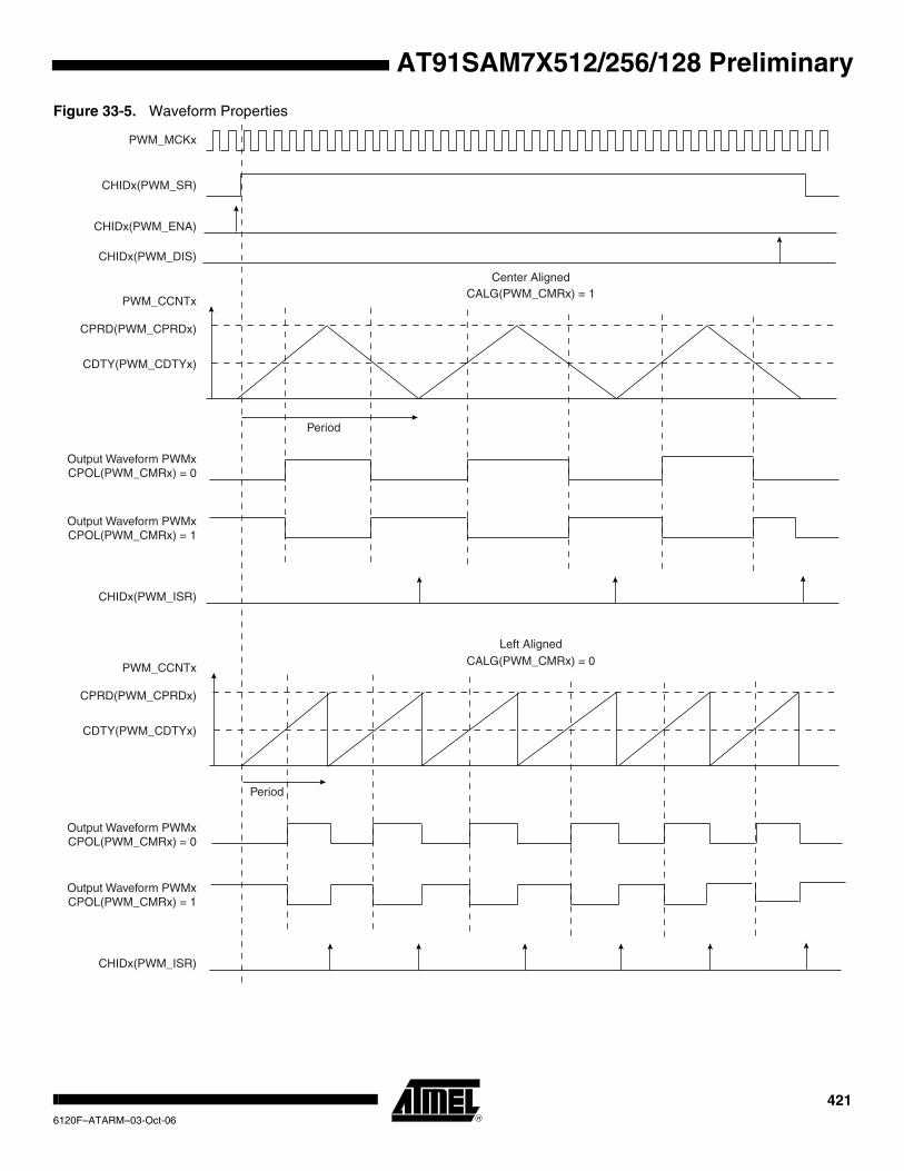
AT91SAM7X512/256/128 Preliminary
Figure 33-5. Waveform Properties
PWM_MCKx
CHIDx(PWM_SR)
Center Aligned
CPRD(PWM_CPRDx)
CDTY(PWM_CDTYx)
PWM_CCNTx
Output Waveform PWMxCPOL(PWM_CMRx) = 0
Output Waveform PWMxCPOL(PWM_CMRx) = 1
CHIDx(PWM_ISR)
Left Aligned
CPRD(PWM_CPRDx)
CDTY(PWM_CDTYx)
PWM_CCNTx
Output Waveform PWMxCPOL(PWM_CMRx) = 0
Output Waveform PWMxCPOL(PWM_CMRx) = 1
CHIDx(PWM_ISR)
CALG(PWM_CMRx) = 0
CALG(PWM_CMRx) = 1
Period
Period
CHIDx(PWM_ENA)
CHIDx(PWM_DIS)
4216120F–ATARM–03-Oct-06

33.5.3 PWM Controller Operations
33.5.3.1 Initialization
Before enabling the output channel, this channel must have been configured by the software application:
• Configuration of the clock generator if DIVA and DIVB are required
• Selection of the clock for each channel (CPRE field in the PWM_CMRx register)
• Configuration of the waveform alignment for each channel (CALG field in the PWM_CMRx register)
• Configuration of the period for each channel (CPRD in the PWM_CPRDx register). Writing in PWM_CPRDx Register is possible while the channel is disabled. After validation of the channel, the user must use PWM_CUPDx Register to update PWM_CPRDx as explained below.
• Configuration of the duty cycle for each channel (CDTY in the PWM_CDTYx register). Writing in PWM_CDTYx Register is possible while the channel is disabled. After validation of the channel, the user must use PWM_CUPDx Register to update PWM_CDTYx as explained below.
• Configuration of the output waveform polarity for each channel (CPOL in the PWM_CMRx register)
• Enable Interrupts (Writing CHIDx in the PWM_IER register)
• Enable the PWM channel (Writing CHIDx in the PWM_ENA register)
It is possible to synchronize different channels by enabling them at the same time by means of writing simultaneously several CHIDx bits in the PWM_ENA register.
• In such a situation, all channels may have the same clock selector configuration and the same period specified.
33.5.3.2 Source Clock Selection Criteria
The large number of source clocks can make selection difficult. The relationship between the value in the Period Register (PWM_CPRDx) and the Duty Cycle Register (PWM_CDTYx) can help the user in choosing. The event number written in the Period Register gives the PWM accu-racy. The Duty Cycle quantum cannot be lower than 1/PWM_CPRDx value. The higher the value of PWM_CPRDx, the greater the PWM accuracy.
For example, if the user sets 15 (in decimal) in PWM_CPRDx, the user is able to set a value between 1 up to 14 in PWM_CDTYx Register. The resulting duty cycle quantum cannot be lower than 1/15 of the PWM period.
33.5.3.3 Changing the Duty Cycle or the Period
It is possible to modulate the output waveform duty cycle or period.
To prevent unexpected output waveform, the user must use the update register (PWM_CUPDx) to change waveform parameters while the channel is still enabled. The user can write a new period value or duty cycle value in the update register (PWM_CUPDx). This register holds the new value until the end of the current cycle and updates the value for the next cycle. Depending on the CPD field in the PWM_CMRx register, PWM_CUPDx either updates PWM_CPRDx or PWM_CDTYx. Note that even if the update register is used, the period must not be smaller than the duty cycle.
4226120F–ATARM–03-Oct-06
AT91SAM7X512/256/128 Preliminary

AT91SAM7X512/256/128 Preliminary
Figure 33-6. Synchronized Period or Duty Cycle Update
To prevent overwriting the PWM_CUPDx by software, the user can use status events in order to synchronize his software. Two methods are possible. In both, the user must enable the dedi-cated interrupt in PWM_IER at PWM Controller level.
The first method (polling method) consists of reading the relevant status bit in PWM_ISR Regis-ter according to the enabled channel(s). See Figure 33-7.
The second method uses an Interrupt Service Routine associated with the PWM channel.
Note: Reading the PWM_ISR register automatically clears CHIDx flags.
Figure 33-7. Polling Method
Note: Polarity and alignment can be modified only when the channel is disabled.
PWM_CUPDx Value
PWM_CPRDx PWM_CDTYx
End of Cycle
PWM_CMRx. CPD
User's Writing
1 0
Writing in PWM_CUPDxThe last write has been taken into account
CHIDx = 1
Writing in CPD fieldUpdate of the Period or Duty Cycle
PWM_ISR ReadAcknowledgement and clear previous register state
YES
4236120F–ATARM–03-Oct-06

33.5.3.4 Interrupts
Depending on the interrupt mask in the PWM_IMR register, an interrupt is generated at the end of the corresponding channel period. The interrupt remains active until a read operation in the PWM_ISR register occurs.
A channel interrupt is enabled by setting the corresponding bit in the PWM_IER register. A chan-nel interrupt is disabled by setting the corresponding bit in the PWM_IDR register.
4246120F–ATARM–03-Oct-06
AT91SAM7X512/256/128 Preliminary

AT91SAM7X512/256/128 Preliminary
33.6 Pulse Width Modulation Controller (PWM) User Interface
Table 33-2. Pulse Width Modulation Controller (PWM) Register Mapping
Offset Register Name AccessPeripheral
Reset Value
0x00 PWM Mode Register PWM_MR Read/Write 0
0x04 PWM Enable Register PWM_ENA Write-only -
0x08 PWM Disable Register PWM_DIS Write-only -
0x0C PWM Status Register PWM_SR Read-only 0
0x10 PWM Interrupt Enable Register PWM_IER Write-only -
0x14 PWM Interrupt Disable Register PWM_IDR Write-only -
0x18 PWM Interrupt Mask Register PWM_IMR Read-only 0
0x1C PWM Interrupt Status Register PWM_ISR Read-only 0
0x4C - 0xFC Reserved – – –
0x100 - 0x1FC Reserved
0x200 Channel 0 Mode Register PWM_CMR0 Read/Write 0x0
0x204 Channel 0 Duty Cycle Register PWM_CDTY0 Read/Write 0x0
0x208 Channel 0 Period Register PWM_CPRD0 Read/Write 0x0
0x20C Channel 0 Counter Register PWM_CCNT0 Read-only 0x0
0x210 Channel 0 Update Register PWM_CUPD0 Write-only -
... Reserved
0x220 Channel 1 Mode Register PWM_CMR1 Read/Write 0x0
0x224 Channel 1 Duty Cycle Register PWM_CDTY1 Read/Write 0x0
0x228 Channel 1 Period Register PWM_CPRD1 Read/Write 0x0
0x22C Channel 1 Counter Register PWM_CCNT1 Read-only 0x0
0x230 Channel 1 Update Register PWM_CUPD1 Write-only -
... ... ... ... ...
4256120F–ATARM–03-Oct-06
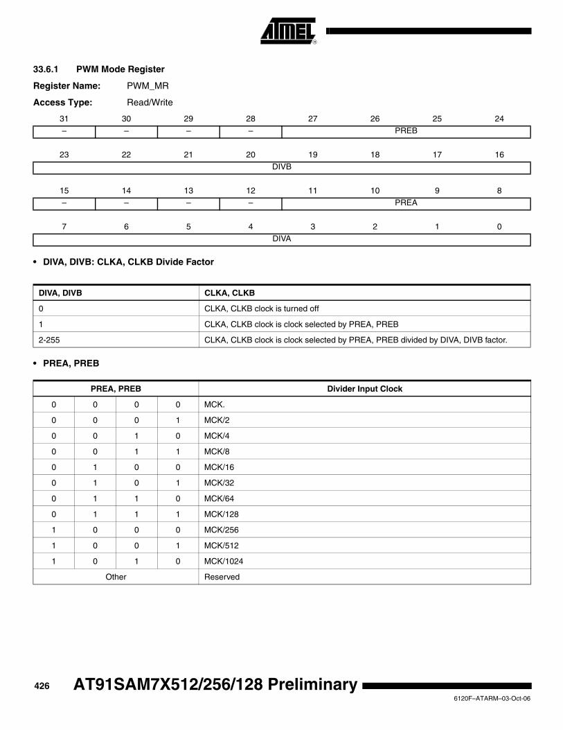
33.6.1 PWM Mode Register
Register Name: PWM_MR
Access Type: Read/Write
• DIVA, DIVB: CLKA, CLKB Divide Factor
• PREA, PREB
31 30 29 28 27 26 25 24– – – – PREB
23 22 21 20 19 18 17 16
DIVB
15 14 13 12 11 10 9 8
– – – – PREA
7 6 5 4 3 2 1 0
DIVA
DIVA, DIVB CLKA, CLKB
0 CLKA, CLKB clock is turned off
1 CLKA, CLKB clock is clock selected by PREA, PREB
2-255 CLKA, CLKB clock is clock selected by PREA, PREB divided by DIVA, DIVB factor.
PREA, PREB Divider Input Clock
0 0 0 0 MCK.
0 0 0 1 MCK/2
0 0 1 0 MCK/4
0 0 1 1 MCK/8
0 1 0 0 MCK/16
0 1 0 1 MCK/32
0 1 1 0 MCK/64
0 1 1 1 MCK/128
1 0 0 0 MCK/256
1 0 0 1 MCK/512
1 0 1 0 MCK/1024
Other Reserved
4266120F–ATARM–03-Oct-06
AT91SAM7X512/256/128 Preliminary

AT91SAM7X512/256/128 Preliminary
33.6.2 PWM Enable Register
Register Name: PWM_ENA
Access Type: Write-only
• CHIDx: Channel ID
0 = No effect.
1 = Enable PWM output for channel x.
33.6.3 PWM Disable Register
Register Name: PWM_DIS
Access Type: Write-only
• CHIDx: Channel ID
0 = No effect.
1 = Disable PWM output for channel x.
31 30 29 28 27 26 25 24– – – – – – – –
23 22 21 20 19 18 17 16
– – – – – – – –
15 14 13 12 11 10 9 8
– – – – – – – –
7 6 5 4 3 2 1 0
– – – – CHID3 CHID2 CHID1 CHID0
31 30 29 28 27 26 25 24
– – – – – – – –
23 22 21 20 19 18 17 16
– – – – – – – –
15 14 13 12 11 10 9 8
– – – – – – – –
7 6 5 4 3 2 1 0
– – – – CHID3 CHID2 CHID1 CHID0
4276120F–ATARM–03-Oct-06
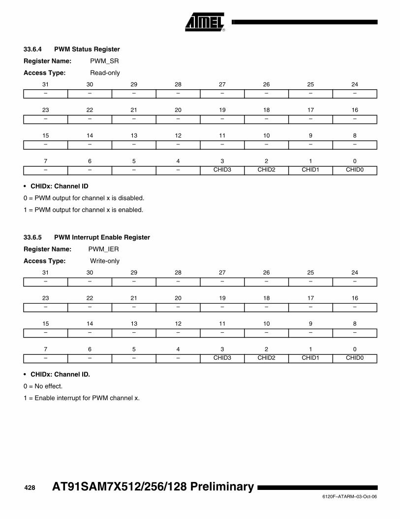
33.6.4 PWM Status Register
Register Name: PWM_SR
Access Type: Read-only
• CHIDx: Channel ID
0 = PWM output for channel x is disabled.
1 = PWM output for channel x is enabled.
33.6.5 PWM Interrupt Enable Register
Register Name: PWM_IER
Access Type: Write-only
• CHIDx: Channel ID.
0 = No effect.
1 = Enable interrupt for PWM channel x.
31 30 29 28 27 26 25 24– – – – – – – –
23 22 21 20 19 18 17 16
– – – – – – – –
15 14 13 12 11 10 9 8
– – – – – – – –
7 6 5 4 3 2 1 0
– – – – CHID3 CHID2 CHID1 CHID0
31 30 29 28 27 26 25 24
– – – – – – – –
23 22 21 20 19 18 17 16
– – – – – – – –
15 14 13 12 11 10 9 8
– – – – – – – –
7 6 5 4 3 2 1 0
– – – – CHID3 CHID2 CHID1 CHID0
4286120F–ATARM–03-Oct-06
AT91SAM7X512/256/128 Preliminary
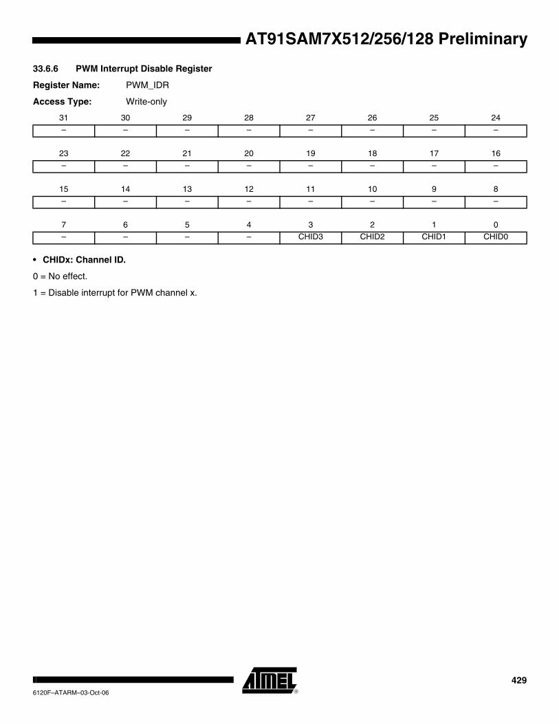
AT91SAM7X512/256/128 Preliminary
33.6.6 PWM Interrupt Disable Register
Register Name: PWM_IDR
Access Type: Write-only
• CHIDx: Channel ID.
0 = No effect.
1 = Disable interrupt for PWM channel x.
31 30 29 28 27 26 25 24– – – – – – – –
23 22 21 20 19 18 17 16
– – – – – – – –
15 14 13 12 11 10 9 8
– – – – – – – –
7 6 5 4 3 2 1 0
– – – – CHID3 CHID2 CHID1 CHID0
4296120F–ATARM–03-Oct-06
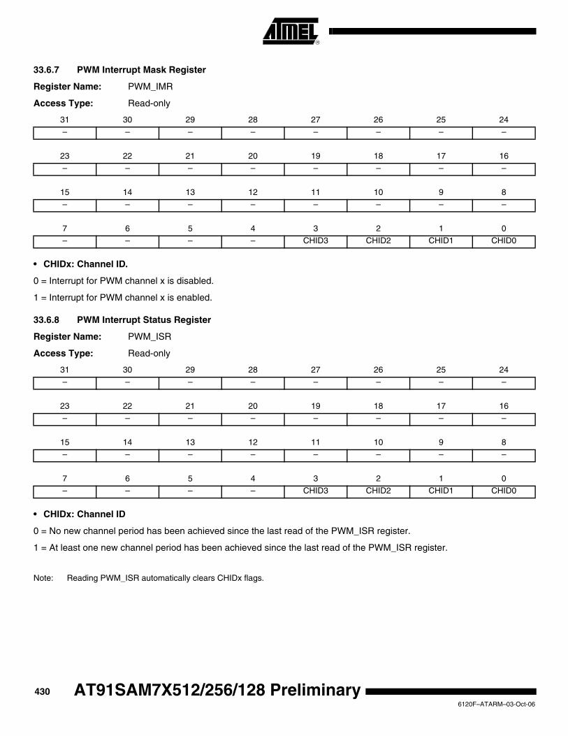
33.6.7 PWM Interrupt Mask Register
Register Name: PWM_IMR
Access Type: Read-only
• CHIDx: Channel ID.
0 = Interrupt for PWM channel x is disabled.
1 = Interrupt for PWM channel x is enabled.
33.6.8 PWM Interrupt Status Register
Register Name: PWM_ISR
Access Type: Read-only
• CHIDx: Channel ID
0 = No new channel period has been achieved since the last read of the PWM_ISR register.
1 = At least one new channel period has been achieved since the last read of the PWM_ISR register.
Note: Reading PWM_ISR automatically clears CHIDx flags.
31 30 29 28 27 26 25 24– – – – – – – –
23 22 21 20 19 18 17 16
– – – – – – – –
15 14 13 12 11 10 9 8
– – – – – – – –
7 6 5 4 3 2 1 0
– – – – CHID3 CHID2 CHID1 CHID0
31 30 29 28 27 26 25 24
– – – – – – – –
23 22 21 20 19 18 17 16
– – – – – – – –
15 14 13 12 11 10 9 8
– – – – – – – –
7 6 5 4 3 2 1 0
– – – – CHID3 CHID2 CHID1 CHID0
4306120F–ATARM–03-Oct-06
AT91SAM7X512/256/128 Preliminary

AT91SAM7X512/256/128 Preliminary
33.6.9 PWM Channel Mode Register
Register Name: PWM_CMRx
Access Type: Read/Write
• CPRE: Channel Pre-scaler
• CALG: Channel Alignment
0 = The period is left aligned.
1 = The period is center aligned.
• CPOL: Channel Polarity
0 = The output waveform starts at a low level.
1 = The output waveform starts at a high level.
• CPD: Channel Update Period
0 = Writing to the PWM_CUPDx will modify the duty cycle at the next period start event.
1 = Writing to the PWM_CUPDx will modify the period at the next period start event.
31 30 29 28 27 26 25 24– – – – – – – –
23 22 21 20 19 18 17 16
– – – – – – – –
15 14 13 12 11 10 9 8
– – – – – CPD CPOL CALG
7 6 5 4 3 2 1 0
– – – – CPRE
CPRE Channel Pre-scaler
0 0 0 0 MCK
0 0 0 1 MCK/2
0 0 1 0 MCK/4
0 0 1 1 MCK/8
0 1 0 0 MCK/16
0 1 0 1 MCK/32
0 1 1 0 MCK/64
0 1 1 1 MCK/128
1 0 0 0 MCK/256
1 0 0 1 MCK/512
1 0 1 0 MCK/1024
1 0 1 1 CLKA
1 1 0 0 CLKB
Other Reserved
4316120F–ATARM–03-Oct-06
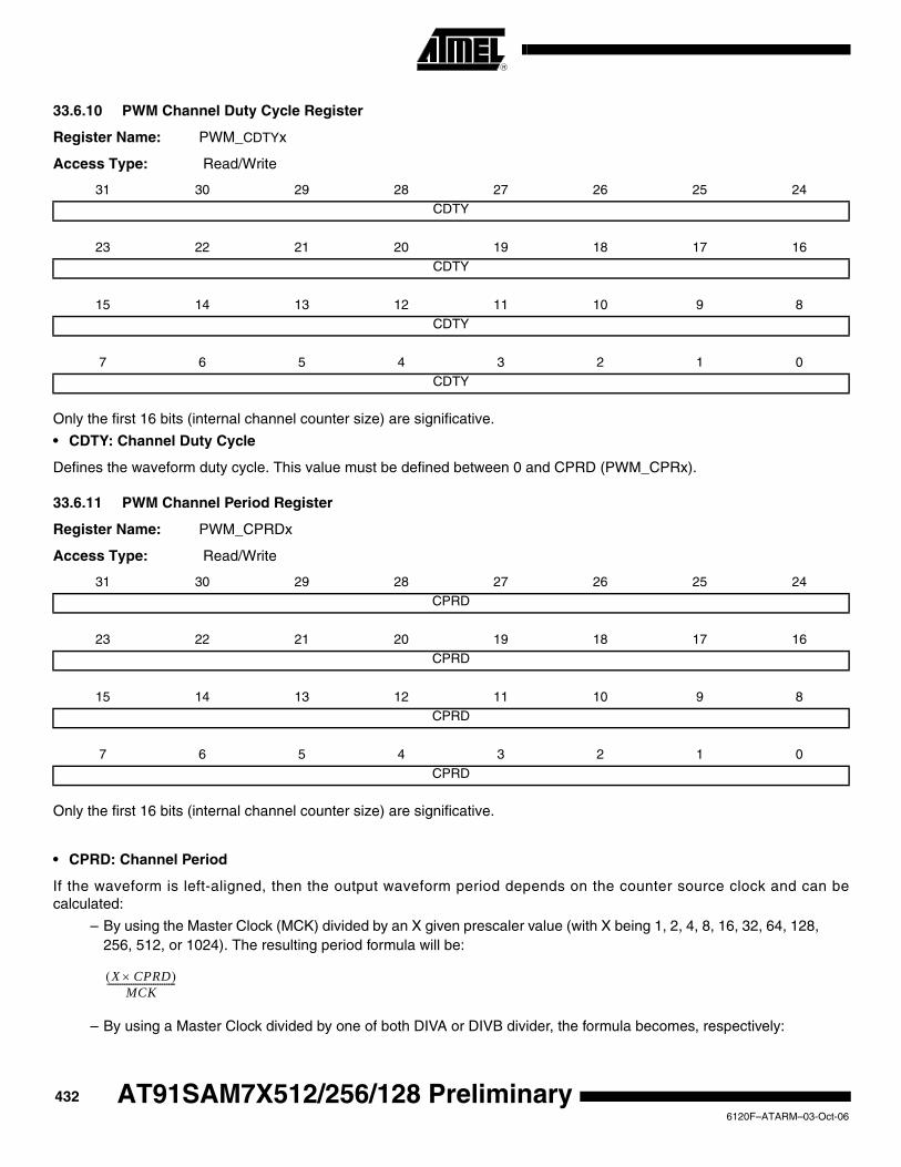
33.6.10 PWM Channel Duty Cycle Register
Register Name: PWM_CDTYx
Access Type: Read/Write
Only the first 16 bits (internal channel counter size) are significative.
• CDTY: Channel Duty Cycle
Defines the waveform duty cycle. This value must be defined between 0 and CPRD (PWM_CPRx).
33.6.11 PWM Channel Period Register
Register Name: PWM_CPRDx
Access Type: Read/Write
Only the first 16 bits (internal channel counter size) are significative.
• CPRD: Channel Period
If the waveform is left-aligned, then the output waveform period depends on the counter source clock and can be calculated:
– By using the Master Clock (MCK) divided by an X given prescaler value (with X being 1, 2, 4, 8, 16, 32, 64, 128, 256, 512, or 1024). The resulting period formula will be:
– By using a Master Clock divided by one of both DIVA or DIVB divider, the formula becomes, respectively:
31 30 29 28 27 26 25 24CDTY
23 22 21 20 19 18 17 16
CDTY
15 14 13 12 11 10 9 8
CDTY
7 6 5 4 3 2 1 0
CDTY
31 30 29 28 27 26 25 24
CPRD
23 22 21 20 19 18 17 16
CPRD
15 14 13 12 11 10 9 8
CPRD
7 6 5 4 3 2 1 0
CPRD
X CPRD×( )MCK
-------------------------------
4326120F–ATARM–03-Oct-06
AT91SAM7X512/256/128 Preliminary
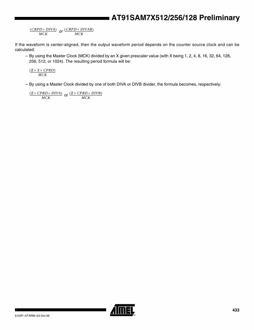
AT91SAM7X512/256/128 Preliminary
or
If the waveform is center-aligned, then the output waveform period depends on the counter source clock and can be calculated:
– By using the Master Clock (MCK) divided by an X given prescaler value (with X being 1, 2, 4, 8, 16, 32, 64, 128, 256, 512, or 1024). The resulting period formula will be:
– By using a Master Clock divided by one of both DIVA or DIVB divider, the formula becomes, respectively:
or
CRPD DIVA×( )MCK
------------------------------------------ CRPD DIVAB×( )MCK
----------------------------------------------
2 X CPRD××( )MCK
-----------------------------------------
2 CPRD DIVA××( )MCK
---------------------------------------------------- 2 CPRD× DIVB×( )MCK
----------------------------------------------------
4336120F–ATARM–03-Oct-06
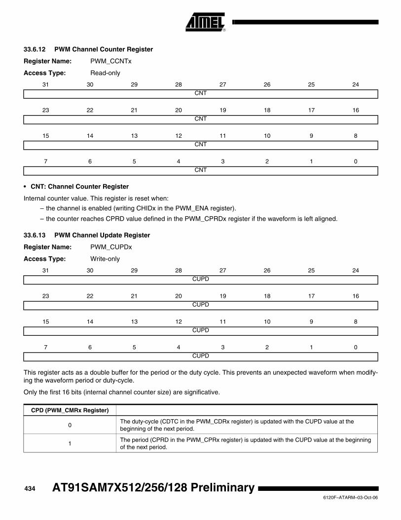
33.6.12 PWM Channel Counter Register
Register Name: PWM_CCNTx
Access Type: Read-only
• CNT: Channel Counter Register
Internal counter value. This register is reset when:
– the channel is enabled (writing CHIDx in the PWM_ENA register).
– the counter reaches CPRD value defined in the PWM_CPRDx register if the waveform is left aligned.
33.6.13 PWM Channel Update Register
Register Name: PWM_CUPDx
Access Type: Write-only
This register acts as a double buffer for the period or the duty cycle. This prevents an unexpected waveform when modify-ing the waveform period or duty-cycle.
Only the first 16 bits (internal channel counter size) are significative.
31 30 29 28 27 26 25 24CNT
23 22 21 20 19 18 17 16
CNT
15 14 13 12 11 10 9 8
CNT
7 6 5 4 3 2 1 0
CNT
31 30 29 28 27 26 25 24CUPD
23 22 21 20 19 18 17 16CUPD
15 14 13 12 11 10 9 8CUPD
7 6 5 4 3 2 1 0CUPD
CPD (PWM_CMRx Register)
0The duty-cycle (CDTC in the PWM_CDRx register) is updated with the CUPD value at the beginning of the next period.
1The period (CPRD in the PWM_CPRx register) is updated with the CUPD value at the beginning of the next period.
4346120F–ATARM–03-Oct-06
AT91SAM7X512/256/128 Preliminary
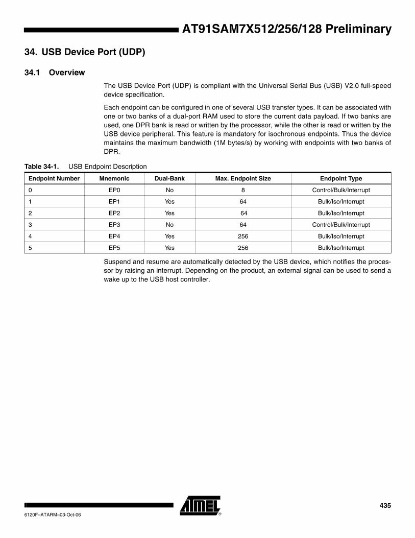
AT91SAM7X512/256/128 Preliminary
34. USB Device Port (UDP)
34.1 Overview
The USB Device Port (UDP) is compliant with the Universal Serial Bus (USB) V2.0 full-speed device specification.
Each endpoint can be configured in one of several USB transfer types. It can be associated with one or two banks of a dual-port RAM used to store the current data payload. If two banks are used, one DPR bank is read or written by the processor, while the other is read or written by the USB device peripheral. This feature is mandatory for isochronous endpoints. Thus the device maintains the maximum bandwidth (1M bytes/s) by working with endpoints with two banks of DPR.
Suspend and resume are automatically detected by the USB device, which notifies the proces-sor by raising an interrupt. Depending on the product, an external signal can be used to send a wake up to the USB host controller.
Table 34-1. USB Endpoint Description
Endpoint Number Mnemonic Dual-Bank Max. Endpoint Size Endpoint Type
0 EP0 No 8 Control/Bulk/Interrupt
1 EP1 Yes 64 Bulk/Iso/Interrupt
2 EP2 Yes 64 Bulk/Iso/Interrupt
3 EP3 No 64 Control/Bulk/Interrupt
4 EP4 Yes 256 Bulk/Iso/Interrupt
5 EP5 Yes 256 Bulk/Iso/Interrupt
4356120F–ATARM–03-Oct-06

34.2 Block Diagram
Figure 34-1. Block Diagram
Access to the UDP is via the APB bus interface. Read and write to the data FIFO are done by reading and writing 8-bit values to APB registers.
The UDP peripheral requires two clocks: one peripheral clock used by the MCK domain and a 48 MHz clock used by the 12 MHz domain.
A USB 2.0 full-speed pad is embedded and controlled by the Serial Interface Engine (SIE).
The signal external_resume is optional. It allows the UDP peripheral to wake up once in system mode. The host is then notified that the device asks for a resume. This optional feature must be also negotiated with the host during the enumeration.
Atmel Bridge
12 MHz
Suspend/Resume Logic
Wrapper
Wrapper
User Interface
SerialInterfaceEngine
SIE
MCK
Master ClockDomain
DualPortRAM
FIFO
UDPCK
Recovered 12 MHzDomain
udp_int
USB Device
EmbeddedUSB
Transceiver
DP
DM
external_resume
APBto
MCUBus
txoen
eopn
txd
rxdm
rxd
rxdp
4366120F–ATARM–03-Oct-06
AT91SAM7X512/256/128 Preliminary
AT91SAM7X512/256/128 Preliminary
34.3 Product Dependencies
For further details on the USB Device hardware implementation, see the specific Product Prop-erties document.
The USB physical transceiver is integrated into the product. The bidirectional differential signals DP and DM are available from the product boundary.
Two I/O lines may be used by the application:
• One to check that VBUS is still available from the host. Self-powered devices may use this entry to be notified that the host has been powered off. In this case, the board pullup on DP must be disabled in order to prevent feeding current to the host.
• One to control the board pullup on DP. Thus, when the device is ready to communicate with the host, it activates its DP pullup through this control line.
34.3.1 I/O Lines
DP and DM are not controlled by any PIO controllers. The embedded USB physical transceiver is controlled by the USB device peripheral.
To reserve an I/O line to check VBUS, the programmer must first program the PIO controller to assign this I/O in input PIO mode.
To reserve an I/O line to control the board pullup, the programmer must first program the PIO controller to assign this I/O in output PIO mode.
34.3.2 Power Management
The USB device peripheral requires a 48 MHz clock. This clock must be generated by a PLL with an accuracy of ± 0.25%.
Thus, the USB device receives two clocks from the Power Management Controller (PMC): the master clock, MCK, used to drive the peripheral user interface, and the UDPCK, used to inter-face with the bus USB signals (recovered 12 MHz domain).
WARNING: The UDP peripheral clock in the Power Management Controller (PMC) must be enabled before any read/write operations to the UDP registers including the UDP_TXCV register.
34.3.3 Interrupt
The USB device interface has an interrupt line connected to the Advanced Interrupt Controller (AIC).
Handling the USB device interrupt requires programming the AIC before configuring the UDP.
4376120F–ATARM–03-Oct-06
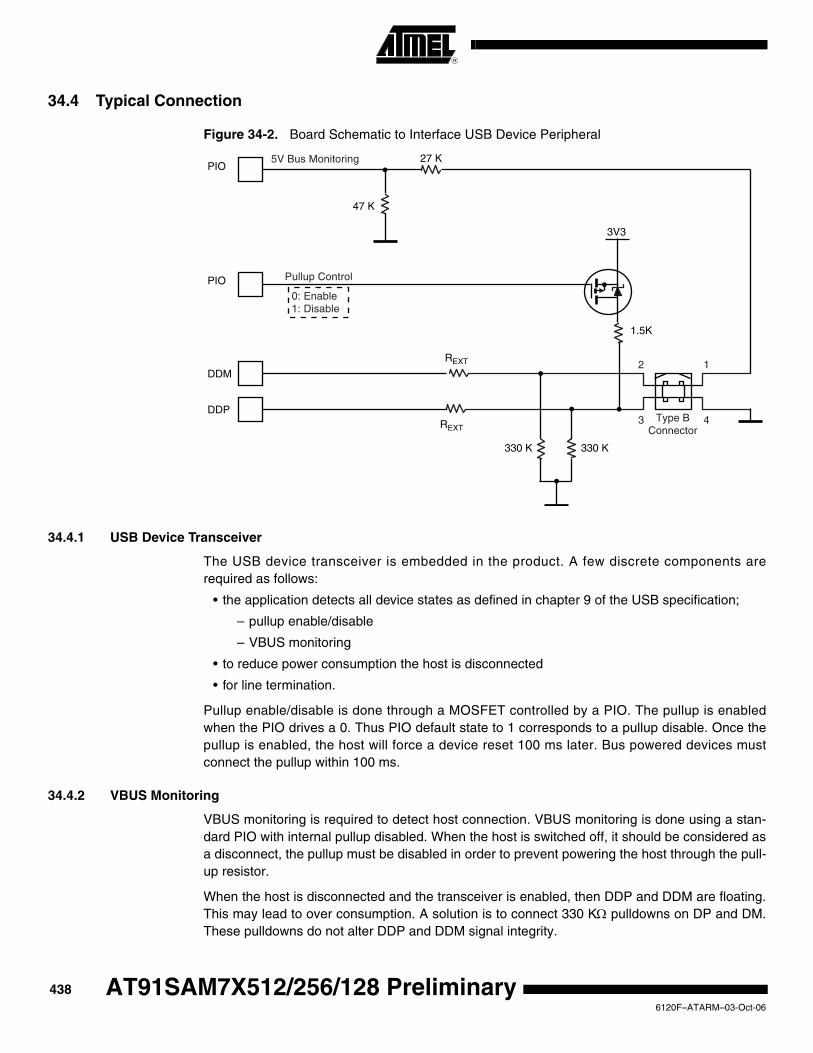
34.4 Typical Connection
Figure 34-2. Board Schematic to Interface USB Device Peripheral
34.4.1 USB Device Transceiver
The USB device transceiver is embedded in the product. A few discrete components are required as follows:
• the application detects all device states as defined in chapter 9 of the USB specification;
– pullup enable/disable
– VBUS monitoring
• to reduce power consumption the host is disconnected
• for line termination.
Pullup enable/disable is done through a MOSFET controlled by a PIO. The pullup is enabled when the PIO drives a 0. Thus PIO default state to 1 corresponds to a pullup disable. Once the pullup is enabled, the host will force a device reset 100 ms later. Bus powered devices must connect the pullup within 100 ms.
34.4.2 VBUS Monitoring
VBUS monitoring is required to detect host connection. VBUS monitoring is done using a stan-dard PIO with internal pullup disabled. When the host is switched off, it should be considered as a disconnect, the pullup must be disabled in order to prevent powering the host through the pull-up resistor.
When the host is disconnected and the transceiver is enabled, then DDP and DDM are floating. This may lead to over consumption. A solution is to connect 330 KΩ pulldowns on DP and DM. These pulldowns do not alter DDP and DDM signal integrity.
3V3
REXT
DDM
DDP
PIO
PIO27 K
47 K
330 K
Type BConnector
12
3 4
5V Bus Monitoring
Pullup Control
REXT
330 K
1.5K
0: Enable1: Disable
4386120F–ATARM–03-Oct-06
AT91SAM7X512/256/128 Preliminary

AT91SAM7X512/256/128 Preliminary
A termination serial resistor must be connected to DP and DM. The resistor value is defined in the electrical specification of the product (REXT).
4396120F–ATARM–03-Oct-06

34.5 Functional Description
34.5.1 USB V2.0 Full-speed Introduction
The USB V2.0 full-speed provides communication services between host and attached USB devices. Each device is offered with a collection of communication flows (pipes) associated with each endpoint. Software on the host communicates with a USB device through a set of commu-nication flows.
Figure 34-3. Example of USB V2.0 Full-speed Communication Control
The Control Transfer endpoint EP0 is always used when a USB device is first configured (USB v. 2.0 specifications).
34.5.1.1 USB V2.0 Full-speed Transfer Types
A communication flow is carried over one of four transfer types defined by the USB device.
34.5.1.2 USB Bus Transactions
Each transfer results in one or more transactions over the USB bus. There are three kinds of transactions flowing across the bus in packets:
EP0
USB Host V2.0
Software Client 1 Software Client 2
Data Flow: Bulk Out Transfer
Data Flow: Bulk In Transfer
Data Flow: Control Transfer
Data Flow: Control Transfer
EP1
EP2
USB Device 2.0 Block 1
USB Device 2.0 Block 2
EP5
EP4
EP0
Data Flow: Isochronous In Transfer
Data Flow: Isochronous Out Transfer
USB Device endpoint configuration requires thatin the first instance Control Transfer must be EP0.
Table 34-2. USB Communication Flow
Transfer Direction Bandwidth Supported Endpoint Size Error Detection Retrying
Control Bidirectional Not guaranteed 8, 16, 32, 64 Yes Automatic
Isochronous Unidirectional Guaranteed 256 Yes No
Interrupt Unidirectional Not guaranteed 8, 16, 32, 64 Yes Yes
Bulk Unidirectional Not guaranteed 8, 16, 32, 64 Yes Yes
4406120F–ATARM–03-Oct-06
AT91SAM7X512/256/128 Preliminary
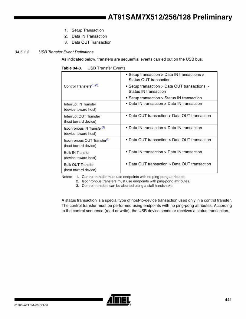
AT91SAM7X512/256/128 Preliminary
1. Setup Transaction
2. Data IN Transaction
3. Data OUT Transaction
34.5.1.3 USB Transfer Event Definitions
As indicated below, transfers are sequential events carried out on the USB bus.
Notes: 1. Control transfer must use endpoints with no ping-pong attributes. 2. Isochronous transfers must use endpoints with ping-pong attributes.3. Control transfers can be aborted using a stall handshake.
A status transaction is a special type of host-to-device transaction used only in a control transfer. The control transfer must be performed using endpoints with no ping-pong attributes. According to the control sequence (read or write), the USB device sends or receives a status transaction.
Table 34-3. USB Transfer Events
Control Transfers(1) (3)
• Setup transaction > Data IN transactions > Status OUT transaction
• Setup transaction > Data OUT transactions > Status IN transaction
• Setup transaction > Status IN transaction
Interrupt IN Transfer(device toward host)
• Data IN transaction > Data IN transaction
Interrupt OUT Transfer(host toward device)
• Data OUT transaction > Data OUT transaction
Isochronous IN Transfer(2)
(device toward host)
• Data IN transaction > Data IN transaction
Isochronous OUT Transfer(2)
(host toward device)
• Data OUT transaction > Data OUT transaction
Bulk IN Transfer (device toward host)
• Data IN transaction > Data IN transaction
Bulk OUT Transfer(host toward device)
• Data OUT transaction > Data OUT transaction
4416120F–ATARM–03-Oct-06
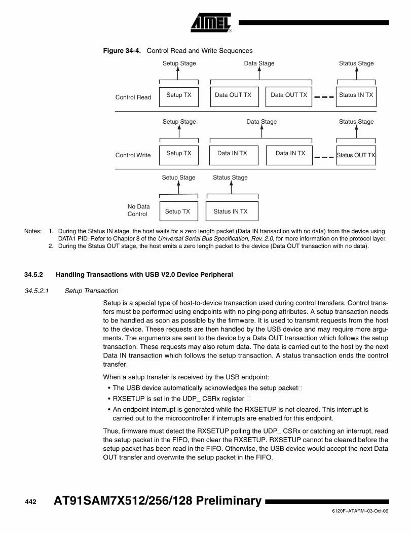
Figure 34-4. Control Read and Write Sequences
Notes: 1. During the Status IN stage, the host waits for a zero length packet (Data IN transaction with no data) from the device using DATA1 PID. Refer to Chapter 8 of the Universal Serial Bus Specification, Rev. 2.0, for more information on the protocol layer.
2. During the Status OUT stage, the host emits a zero length packet to the device (Data OUT transaction with no data).
34.5.2 Handling Transactions with USB V2.0 Device Peripheral
34.5.2.1 Setup Transaction
Setup is a special type of host-to-device transaction used during control transfers. Control trans-fers must be performed using endpoints with no ping-pong attributes. A setup transaction needs to be handled as soon as possible by the firmware. It is used to transmit requests from the host to the device. These requests are then handled by the USB device and may require more argu-ments. The arguments are sent to the device by a Data OUT transaction which follows the setup transaction. These requests may also return data. The data is carried out to the host by the next Data IN transaction which follows the setup transaction. A status transaction ends the control transfer.
When a setup transfer is received by the USB endpoint:
• The USB device automatically acknowledges the setup packet.
• RXSETUP is set in the UDP_ CSRx register .
• An endpoint interrupt is generated while the RXSETUP is not cleared. This interrupt is carried out to the microcontroller if interrupts are enabled for this endpoint.
Thus, firmware must detect the RXSETUP polling the UDP_ CSRx or catching an interrupt, read the setup packet in the FIFO, then clear the RXSETUP. RXSETUP cannot be cleared before the setup packet has been read in the FIFO. Otherwise, the USB device would accept the next Data OUT transfer and overwrite the setup packet in the FIFO.
Control Read Setup TX Data OUT TX Data OUT TX
Data Stage
Control Write
Setup Stage
Setup Stage
Setup TX
Setup TXNo DataControl
Data IN TX Data IN TX
Status Stage
Status Stage
Status IN TX
Status OUT TX
Status IN TX
Data Stage
Setup Stage Status Stage
4426120F–ATARM–03-Oct-06
AT91SAM7X512/256/128 Preliminary
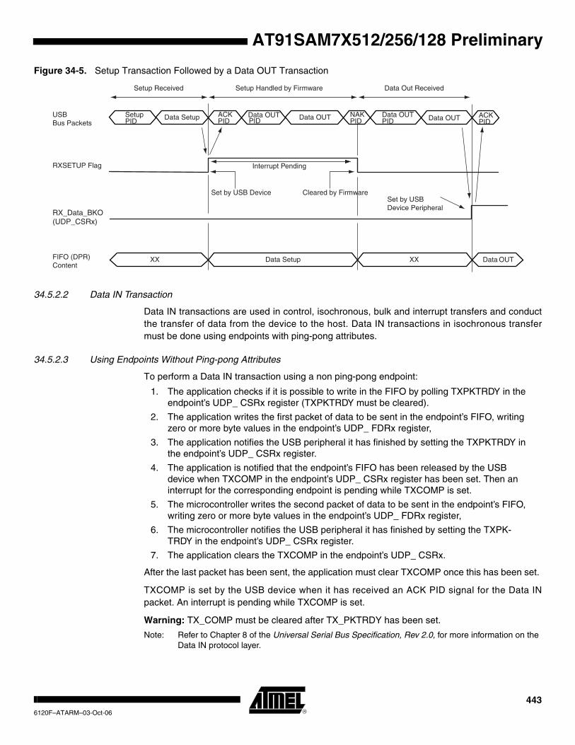
AT91SAM7X512/256/128 Preliminary
Figure 34-5. Setup Transaction Followed by a Data OUT Transaction
34.5.2.2 Data IN Transaction
Data IN transactions are used in control, isochronous, bulk and interrupt transfers and conduct the transfer of data from the device to the host. Data IN transactions in isochronous transfer must be done using endpoints with ping-pong attributes.
34.5.2.3 Using Endpoints Without Ping-pong Attributes
To perform a Data IN transaction using a non ping-pong endpoint:
1. The application checks if it is possible to write in the FIFO by polling TXPKTRDY in the endpoint’s UDP_ CSRx register (TXPKTRDY must be cleared).
2. The application writes the first packet of data to be sent in the endpoint’s FIFO, writing zero or more byte values in the endpoint’s UDP_ FDRx register,
3. The application notifies the USB peripheral it has finished by setting the TXPKTRDY in the endpoint’s UDP_ CSRx register.
4. The application is notified that the endpoint’s FIFO has been released by the USB device when TXCOMP in the endpoint’s UDP_ CSRx register has been set. Then an interrupt for the corresponding endpoint is pending while TXCOMP is set.
5. The microcontroller writes the second packet of data to be sent in the endpoint’s FIFO, writing zero or more byte values in the endpoint’s UDP_ FDRx register,
6. The microcontroller notifies the USB peripheral it has finished by setting the TXPK-TRDY in the endpoint’s UDP_ CSRx register.
7. The application clears the TXCOMP in the endpoint’s UDP_ CSRx.
After the last packet has been sent, the application must clear TXCOMP once this has been set.
TXCOMP is set by the USB device when it has received an ACK PID signal for the Data IN packet. An interrupt is pending while TXCOMP is set.
Warning: TX_COMP must be cleared after TX_PKTRDY has been set.
Note: Refer to Chapter 8 of the Universal Serial Bus Specification, Rev 2.0, for more information on the Data IN protocol layer.
RX_Data_BKO(UDP_CSRx)
ACKPIDData OUTData OUT
PIDNAKPID
ACKPIDData SetupSetup
PIDUSBBus Packets
RXSETUP Flag
Set by USB Device Cleared by FirmwareSet by USB Device Peripheral
FIFO (DPR) Content
Data Setup DataXX XX OUT
Interrupt Pending
Setup Received Setup Handled by Firmware Data Out Received
Data OUTData OUTPID
4436120F–ATARM–03-Oct-06
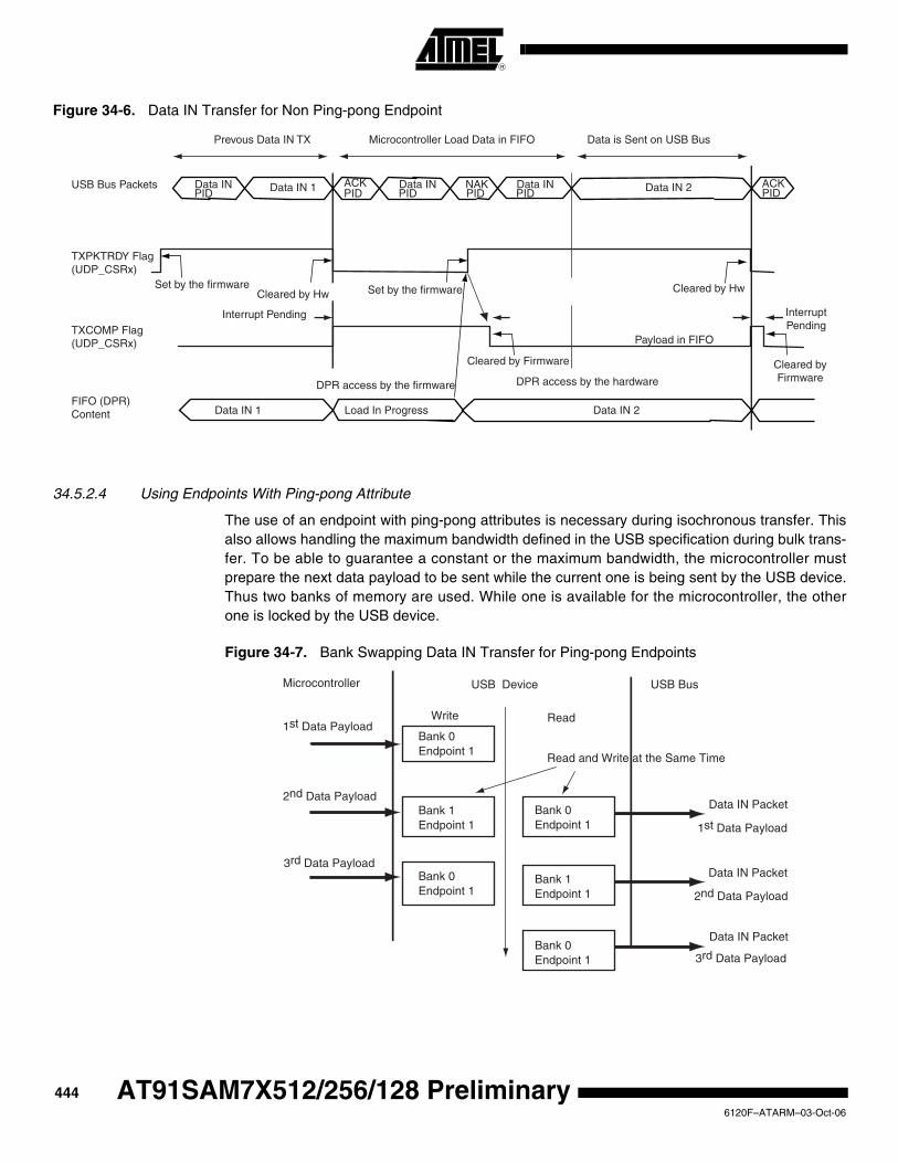
Figure 34-6. Data IN Transfer for Non Ping-pong Endpoint
34.5.2.4 Using Endpoints With Ping-pong Attribute
The use of an endpoint with ping-pong attributes is necessary during isochronous transfer. This also allows handling the maximum bandwidth defined in the USB specification during bulk trans-fer. To be able to guarantee a constant or the maximum bandwidth, the microcontroller must prepare the next data payload to be sent while the current one is being sent by the USB device. Thus two banks of memory are used. While one is available for the microcontroller, the other one is locked by the USB device.
Figure 34-7. Bank Swapping Data IN Transfer for Ping-pong Endpoints
USB Bus Packets Data IN 2Data IN NAKACKData IN 1
FIFO (DPR)Content Data IN 2Load In ProgressData IN 1
Cleared by Firmware
DPR access by the firmware
Payload in FIFOTXCOMP Flag(UDP_CSRx)
TXPKTRDY Flag(UDP_CSRx)
PIDData IN Data IN
PIDPID PIDPIDACKPID
Prevous Data IN TX Microcontroller Load Data in FIFO Data is Sent on USB Bus
InterruptPending
Interrupt Pending
Set by the firmware Set by the firmware
Cleared byFirmware
Cleared by HwCleared by Hw
DPR access by the hardware
USB Device USB Bus
ReadWrite
Read and Write at the Same Time
1st Data Payload
2nd Data Payload
3rd Data Payload
3rd Data Payload
2nd Data Payload
1st Data Payload
Data IN Packet
Data IN Packet
Data IN Packet
Microcontroller
Endpoint 1Bank 0
Endpoint 1Bank 1
Endpoint 1Bank 0
Endpoint 1Bank 0
Endpoint 1Bank 0
Endpoint 1Bank 1
4446120F–ATARM–03-Oct-06
AT91SAM7X512/256/128 Preliminary
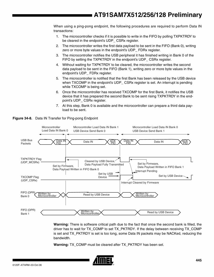
AT91SAM7X512/256/128 Preliminary
When using a ping-pong endpoint, the following procedures are required to perform Data IN transactions:
1. The microcontroller checks if it is possible to write in the FIFO by polling TXPKTRDY to be cleared in the endpoint’s UDP_ CSRx register.
2. The microcontroller writes the first data payload to be sent in the FIFO (Bank 0), writing zero or more byte values in the endpoint’s UDP_ FDRx register.
3. The microcontroller notifies the USB peripheral it has finished writing in Bank 0 of the FIFO by setting the TXPKTRDY in the endpoint’s UDP_ CSRx register.
4. Without waiting for TXPKTRDY to be cleared, the microcontroller writes the second data payload to be sent in the FIFO (Bank 1), writing zero or more byte values in the endpoint’s UDP_ FDRx register.
5. The microcontroller is notified that the first Bank has been released by the USB device when TXCOMP in the endpoint’s UDP_ CSRx register is set. An interrupt is pending while TXCOMP is being set.
6. Once the microcontroller has received TXCOMP for the first Bank, it notifies the USB device that it has prepared the second Bank to be sent rising TXPKTRDY in the end-point’s UDP_ CSRx register.
7. At this step, Bank 0 is available and the microcontroller can prepare a third data pay-load to be sent.
Figure 34-8. Data IN Transfer for Ping-pong Endpoint
Warning: There is software critical path due to the fact that once the second bank is filled, the driver has to wait for TX_COMP to set TX_PKTRDY. If the delay between receiving TX_COMP is set and TX_PKTRDY is set is too long, some Data IN packets may be NACKed, reducing the bandwidth.
Warning: TX_COMP must be cleared after TX_PKTRDY has been set.
Data INData IN
Read by USB Device
Read by USB DeviceBank 1
Bank 0FIFO (DPR)
TXCOMP Flag(UDP_CSRx)
Interrupt Cleared by Firmware
Set by USB Device
TXPKTRDY Flag(UDP_MCSRx)
ACKPID
Data INPID
ACKPID
Set by Firmware,Data Payload Written in FIFO Bank 1
Cleared by USB Device,Data Payload Fully Transmitted
Data INPID
USB BusPackets
Set by USB Device
Set by Firmware,Data Payload Written in FIFO Bank 0
Written by FIFO (DPR) Microcontroller
Written by Microcontroller
Written by Microcontroller
Microcontroller Load Data IN Bank 0
Microcontroller Load Data IN Bank 1USB Device Send Bank 0
Microcontroller Load Data IN Bank 0USB Device Send Bank 1
Interrupt Pending
4456120F–ATARM–03-Oct-06
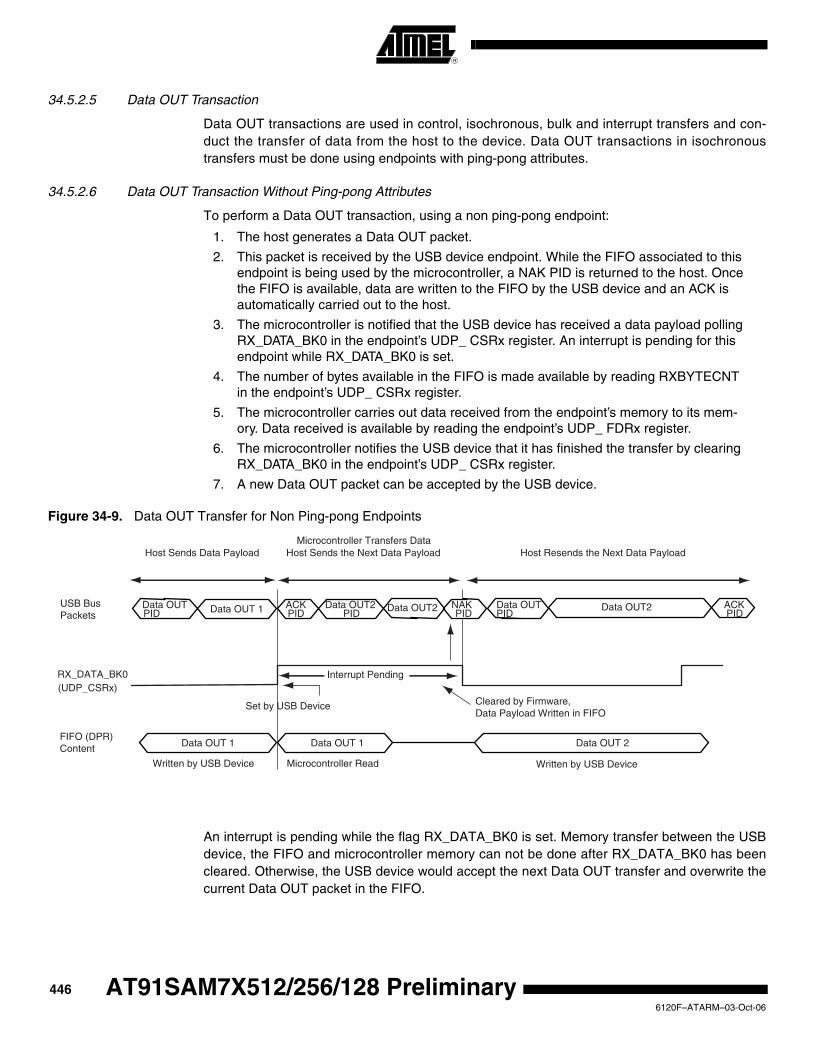
34.5.2.5 Data OUT Transaction
Data OUT transactions are used in control, isochronous, bulk and interrupt transfers and con-duct the transfer of data from the host to the device. Data OUT transactions in isochronous transfers must be done using endpoints with ping-pong attributes.
34.5.2.6 Data OUT Transaction Without Ping-pong Attributes
To perform a Data OUT transaction, using a non ping-pong endpoint:
1. The host generates a Data OUT packet.
2. This packet is received by the USB device endpoint. While the FIFO associated to this endpoint is being used by the microcontroller, a NAK PID is returned to the host. Once the FIFO is available, data are written to the FIFO by the USB device and an ACK is automatically carried out to the host.
3. The microcontroller is notified that the USB device has received a data payload polling RX_DATA_BK0 in the endpoint’s UDP_ CSRx register. An interrupt is pending for this endpoint while RX_DATA_BK0 is set.
4. The number of bytes available in the FIFO is made available by reading RXBYTECNT in the endpoint’s UDP_ CSRx register.
5. The microcontroller carries out data received from the endpoint’s memory to its mem-ory. Data received is available by reading the endpoint’s UDP_ FDRx register.
6. The microcontroller notifies the USB device that it has finished the transfer by clearing RX_DATA_BK0 in the endpoint’s UDP_ CSRx register.
7. A new Data OUT packet can be accepted by the USB device.
Figure 34-9. Data OUT Transfer for Non Ping-pong Endpoints
An interrupt is pending while the flag RX_DATA_BK0 is set. Memory transfer between the USB device, the FIFO and microcontroller memory can not be done after RX_DATA_BK0 has been cleared. Otherwise, the USB device would accept the next Data OUT transfer and overwrite the current Data OUT packet in the FIFO.
ACKPID
Data OUTNAKPIDPIDPIDPIDPID
Data OUT2ACKData OUT Data OUT 1USB BusPackets
RX_DATA_BK0
Set by USB Device Cleared by Firmware,Data Payload Written in FIFO
FIFO (DPR)Content
Written by USB Device Microcontroller Read
Data OUT 1 Data OUT 1 Data OUT 2
Host Resends the Next Data PayloadMicrocontroller Transfers Data
Host Sends Data Payload
Data OUT2 Data OUT2
Host Sends the Next Data Payload
Written by USB Device
(UDP_CSRx)Interrupt Pending
4466120F–ATARM–03-Oct-06
AT91SAM7X512/256/128 Preliminary

AT91SAM7X512/256/128 Preliminary
34.5.2.7 Using Endpoints With Ping-pong Attributes
During isochronous transfer, using an endpoint with ping-pong attributes is obligatory. To be able to guarantee a constant bandwidth, the microcontroller must read the previous data pay-load sent by the host, while the current data payload is received by the USB device. Thus two banks of memory are used. While one is available for the microcontroller, the other one is locked by the USB device.
Figure 34-10. Bank Swapping in Data OUT Transfers for Ping-pong Endpoints
When using a ping-pong endpoint, the following procedures are required to perform Data OUT transactions:
1. The host generates a Data OUT packet.
2. This packet is received by the USB device endpoint. It is written in the endpoint’s FIFO Bank 0.
3. The USB device sends an ACK PID packet to the host. The host can immediately send a second Data OUT packet. It is accepted by the device and copied to FIFO Bank 1.
4. The microcontroller is notified that the USB device has received a data payload, polling RX_DATA_BK0 in the endpoint’s UDP_ CSRx register. An interrupt is pending for this endpoint while RX_DATA_BK0 is set.
5. The number of bytes available in the FIFO is made available by reading RXBYTECNT in the endpoint’s UDP_ CSRx register.
6. The microcontroller transfers out data received from the endpoint’s memory to the microcontroller’s memory. Data received is made available by reading the endpoint’s UDP_ FDRx register.
7. The microcontroller notifies the USB peripheral device that it has finished the transfer by clearing RX_DATA_BK0 in the endpoint’s UDP_ CSRx register.
8. A third Data OUT packet can be accepted by the USB peripheral device and copied in the FIFO Bank 0.
9. If a second Data OUT packet has been received, the microcontroller is notified by the flag RX_DATA_BK1 set in the endpoint’s UDP_ CSRx register. An interrupt is pending for this endpoint while RX_DATA_BK1 is set.
USB Device USB Bus
ReadWrite
Write and Read at the Same Time
1st Data Payload
2nd Data Payload
3rd Data Payload
3rd Data Payload
2nd Data Payload
1st Data Payload
Data IN Packet
Data IN Packet
Data IN Packet
Microcontroller
Endpoint 1Bank 0
Endpoint 1Bank 1
Endpoint 1Bank 0
Endpoint 1Bank 0
Endpoint 1Bank 0
Endpoint 1Bank 1
4476120F–ATARM–03-Oct-06

10. The microcontroller transfers out data received from the endpoint’s memory to the microcontroller’s memory. Data received is available by reading the endpoint’s UDP_ FDRx register.
11. The microcontroller notifies the USB device it has finished the transfer by clearing RX_DATA_BK1 in the endpoint’s UDP_ CSRx register.
12. A fourth Data OUT packet can be accepted by the USB device and copied in the FIFO Bank 0.
Figure 34-11. Data OUT Transfer for Ping-pong Endpoint
Note: An interrupt is pending while the RX_DATA_BK0 or RX_DATA_BK1 flag is set.
Warning: When RX_DATA_BK0 and RX_DATA_BK1 are both set, there is no way to determine which one to clear first. Thus the software must keep an internal counter to be sure to clear alter-natively RX_DATA_BK0 then RX_DATA_BK1. This situation may occur when the software application is busy elsewhere and the two banks are filled by the USB host. Once the application comes back to the USB driver, the two flags are set.
34.5.2.8 Stall Handshake
A stall handshake can be used in one of two distinct occasions. (For more information on the stall handshake, refer to Chapter 8 of the Universal Serial Bus Specification, Rev 2.0.)
• A functional stall is used when the halt feature associated with the endpoint is set. (Refer to Chapter 9 of the Universal Serial Bus Specification, Rev 2.0, for more information on the halt feature.)
• To abort the current request, a protocol stall is used, but uniquely with control transfer.
The following procedure generates a stall packet:
AP
Data OUTPID
ACK Data OUT 3Data OUTData OUT 2Data OUTData OUT 1PID
Data OUT 3Data OUT 1Data OUT1
Data OUT 2 Data OUT 2
PID PID PIDACK
Cleared by Firmware
USB BusPackets
RX_DATA_BK0 Flag
RX_DATA_BK1 Flag
Set by USB Device,Data Payload Writtenin FIFO Endpoint Bank 1
FIFO (DPR) Bank 0
Bank 1
Write by USB Device Write In Progress
Read By Microcontroller
Read By Microcontroller
Set by USB Device,Data Payload Writtenin FIFO Endpoint Bank 0
Host Sends First Data Payload Microcontroller Reads Data 1 in Bank 0, Host Sends Second Data Payload
Microcontroller Reads Data2 in Bank 1, Host Sends Third Data Payload
Cleared by Firmware
Write by USB Device
FIFO (DPR)
(UDP_CSRx)
(UDP_CSRx)
Interrupt Pending
Interrupt Pending
4486120F–ATARM–03-Oct-06
AT91SAM7X512/256/128 Preliminary
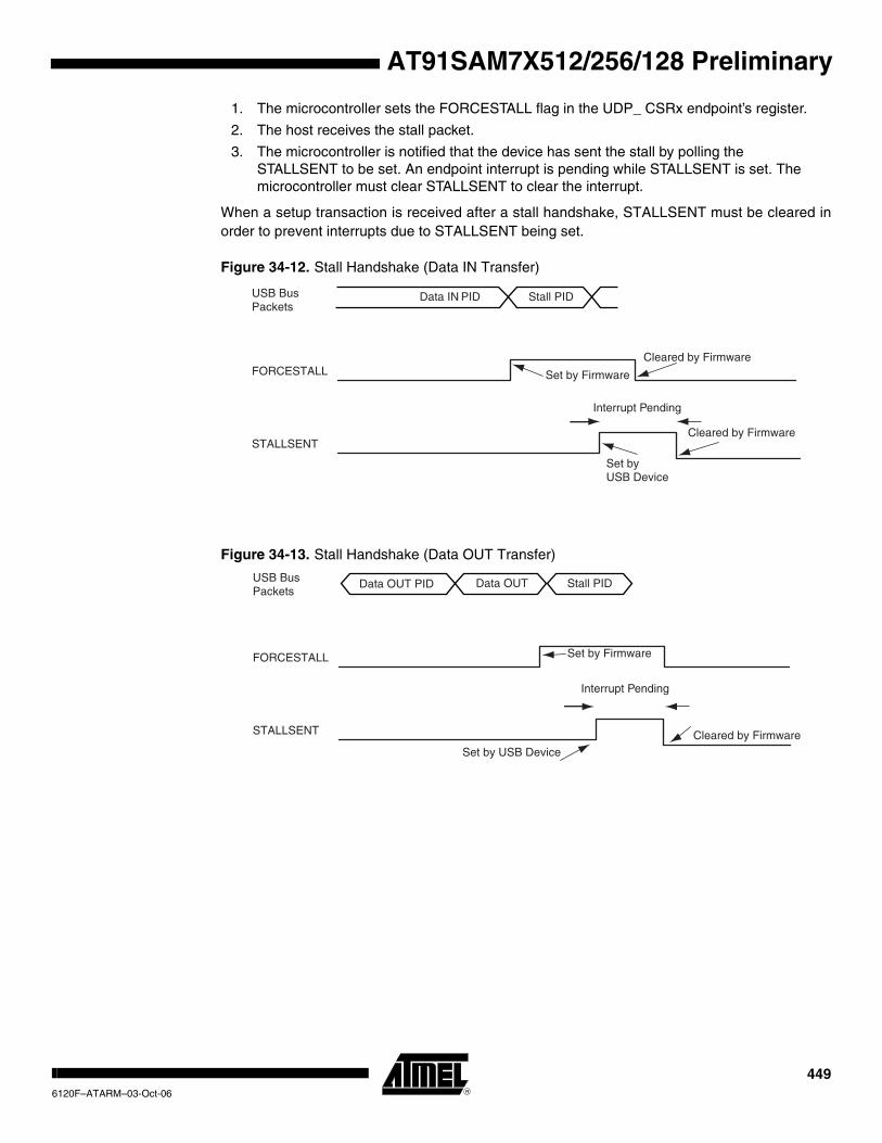
AT91SAM7X512/256/128 Preliminary
1. The microcontroller sets the FORCESTALL flag in the UDP_ CSRx endpoint’s register.
2. The host receives the stall packet.
3. The microcontroller is notified that the device has sent the stall by polling the STALLSENT to be set. An endpoint interrupt is pending while STALLSENT is set. The microcontroller must clear STALLSENT to clear the interrupt.
When a setup transaction is received after a stall handshake, STALLSENT must be cleared in order to prevent interrupts due to STALLSENT being set.
Figure 34-12. Stall Handshake (Data IN Transfer)
Figure 34-13. Stall Handshake (Data OUT Transfer)
Data IN Stall PIDPIDUSB BusPackets
Cleared by Firmware
Set by FirmwareFORCESTALL
STALLSENT
Set byUSB Device
Cleared by Firmware
Interrupt Pending
Data OUT PID Stall PID Data OUTUSB BusPackets
Cleared by Firmware
Set by FirmwareFORCESTALL
STALLSENT
Set by USB Device
Interrupt Pending
4496120F–ATARM–03-Oct-06

34.5.3 Controlling Device States
A USB device has several possible states. Refer to Chapter 9 of the Universal Serial Bus Speci-fication, Rev 2.0.
Figure 34-14. USB Device State Diagram
Movement from one state to another depends on the USB bus state or on standard requests sent through control transactions via the default endpoint (endpoint 0).
After a period of bus inactivity, the USB device enters Suspend Mode. Accepting Sus-pend/Resume requests from the USB host is mandatory. Constraints in Suspend Mode are very strict for bus-powered applications; devices may not consume more than 500 µA on the USB bus.
While in Suspend Mode, the host may wake up a device by sending a resume signal (bus activ-ity) or a USB device may send a wake up request to the host, e.g., waking up a PC by moving a USB mouse.
The wake up feature is not mandatory for all devices and must be negotiated with the host.
Attached
Suspended
Suspended
Suspended
Suspended
Hub Resetor
Deconfigured
HubConfigured
Bus Inactive
Bus Activity
Bus Inactive
Bus Activity
Bus Inactive
Bus Activity
Bus Inactive
Bus Activity
Reset
Reset
AddressAssigned
DeviceDeconfigured
DeviceConfigured
Powered
Default
Address
Configured
PowerInterruption
4506120F–ATARM–03-Oct-06
AT91SAM7X512/256/128 Preliminary
AT91SAM7X512/256/128 Preliminary
34.5.3.1 Not Powered State
Self powered devices can detect 5V VBUS using a PIO as described in the typical connection section. When the device is not connected to a host, device power consumption can be reduced by disabling MCK for the UDP, disabling UDPCK and disabling the transceiver. DDP and DDM lines are pulled down by 330 KΩ resistors.
34.5.3.2 Entering Attached State
When no device is connected, the USB DP and DM signals are tied to GND by 15 KΩ pull-down resistors integrated in the hub downstream ports. When a device is attached to a hub down-stream port, the device connects a 1.5 KΩ pull-up resistor on DP. The USB bus line goes into IDLE state, DP is pulled up by the device 1.5 KΩ resistor to 3.3V and DM is pulled down by the 15 KΩ resistor of the host.
After pullup connection, the device enters the powered state. In this state, the UDPCK and MCK must be enabled in the Power Management Controller. The transceiver can remain disabled.
34.5.3.3 From Powered State to Default State
After its connection to a USB host, the USB device waits for an end-of-bus reset. The unmaskable flag ENDBUSRES is set in the register UDP_ISR and an interrupt is triggered.
Once the ENDBUSRES interrupt has been triggered, the device enters Default State. In this state, the UDP software must:
• Enable the default endpoint, setting the EPEDS flag in the UDP_CSR[0] register and, optionally, enabling the interrupt for endpoint 0 by writing 1 to the UDP_IER register. The enumeration then begins by a control transfer.
• Configure the interrupt mask register which has been reset by the USB reset detection
• Enable the transceiver clearing the TXVDIS flag in the UDP_TXVC register.
In this state UDPCK and MCK must be enabled.
Warning: Each time an ENDBUSRES interrupt is triggered, the Interrupt Mask Register and UDP_CSR registers have been reset.
34.5.3.4 From Default State to Address State
After a set address standard device request, the USB host peripheral enters the address state.
Warning: Before the device enters in address state, it must achieve the Status IN transaction of the control transfer, i.e., the UDP device sets its new address once the TXCOMP flag in the UDP_CSR[0] register has been received and cleared.
To move to address state, the driver software sets the FADDEN flag in the UDP_GLB_STAT register, sets its new address, and sets the FEN bit in the UDP_FADDR register.
34.5.3.5 From Address State to Configured State
Once a valid Set Configuration standard request has been received and acknowledged, the device enables endpoints corresponding to the current configuration. This is done by setting the EPEDS and EPTYPE fields in the UDP_CSRx registers and, optionally, enabling corresponding interrupts in the UDP_IER register.
4516120F–ATARM–03-Oct-06
34.5.3.6 Entering in Suspend State
When a Suspend (no bus activity on the USB bus) is detected, the RXSUSP signal in the UDP_ISR register is set. This triggers an interrupt if the corresponding bit is set in the UDP_IMR register.This flag is cleared by writing to the UDP_ICR register. Then the device enters Suspend Mode.
In this state bus powered devices must drain less than 500uA from the 5V VBUS. As an exam-ple, the microcontroller switches to slow clock, disables the PLL and main oscillator, and goes into Idle Mode. It may also switch off other devices on the board.
The USB device peripheral clocks can be switched off. Resume event is asynchronously detected. MCK and UDPCK can be switched off in the Power Management controller and the USB transceiver can be disabled by setting the TXVDIS field in the UDP_TXVC register.
Warning: Read, write operations to the UDP registers are allowed only if MCK is enabled for the UDP peripheral. Switching off MCK for the UDP peripheral must be one of the last operations after writing to the UDP_TXVC and acknowledging the RXSUSP.
34.5.3.7 Receiving a Host Resume
In suspend mode, a resume event on the USB bus line is detected asynchronously, transceiver and clocks are disabled (however the pullup shall not be removed).
Once the resume is detected on the bus, the WAKEUP signal in the UDP_ISR is set. It may gen-erate an interrupt if the corresponding bit in the UDP_IMR register is set. This interrupt may be used to wake up the core, enable PLL and main oscillators and configure clocks.
Warning: Read, write operations to the UDP registers are allowed only if MCK is enabled for the UDP peripheral. MCK for the UDP must be enabled before clearing the WAKEUP bit in the UDP_ICR register and clearing TXVDIS in the UDP_TXVC register.
34.5.3.8 Sending a Device Remote Wakeup
In Suspend state it is possible to wake up the host sending an external resume.
• The device must wait at least 5 ms after being entered in suspend before sending an external resume.
• The device has 10 ms from the moment it starts to drain current and it forces a K state to resume the host.
• The device must force a K state from 1 to 15 ms to resume the host
To force a K state to the bus (DM at 3.3V and DP tied to GND), it is possible to use a transistor to connect a pullup on DM. The K state is obtained by disabling the pullup on DP and enabling the pullup on DM. This should be under the control of the application.
4526120F–ATARM–03-Oct-06
AT91SAM7X512/256/128 Preliminary

AT91SAM7X512/256/128 Preliminary
Figure 34-15. Board Schematic to Drive a K State
3V3
PIO
1.5 K
0: Force Wake UP (K State)1: Normal Mode
DM
4536120F–ATARM–03-Oct-06

34.6 USB Device Port (UDP) User InterfaceWARNING: The UDP peripheral clock in the Power Management Controller (PMC) must be enabled before any read/write operations to the UDP registers including the UDP_TXCV register.
Notes: 1. The addresses of the UDP_ CSRx registers are calculated as: 0x030 + 4(Endpoint Number - 1).2. The addresses of the UDP_ FDRx registers are calculated as: 0x050 + 4(Endpoint Number - 1).3. See Warning above the ”UDP Memory Map” on this page.
Table 34-4. UDP Memory Map
Offset Register Name Access Reset State
0x000 Frame Number Register UDP_ FRM_NUM Read 0x0000_0000
0x004 Global State Register UDP_ GLB_STAT Read/Write 0x0000_0000
0x008 Function Address Register UDP_ FADDR Read/Write 0x0000_0100
0x00C Reserved – – –
0x010 Interrupt Enable Register UDP_ IER Write
0x014 Interrupt Disable Register UDP_ IDR Write
0x018 Interrupt Mask Register UDP_ IMR Read 0x0000_1200
0x01C Interrupt Status Register UDP_ ISR Read 0x0000_XX00
0x020 Interrupt Clear Register UDP_ ICR Write
0x024 Reserved – – –
0x028 Reset Endpoint Register UDP_ RST_EP Read/Write
0x02C Reserved – – –
0x030 Endpoint 0 Control and Status Register UDP_CSR0 Read/Write 0x0000_0000
.
.
.
.
.
.
See Note: (1) Endpoint 5 Control and Status Register UDP_CSR5 Read/Write 0x0000_0000
0x050 Endpoint 0 FIFO Data Register UDP_ FDR0 Read/Write 0x0000_0000
.
.
.
.
.
.
See Note: (2) Endpoint 5 FIFO Data Register UDP_ FDR5 Read/Write 0x0000_0000
0x070 Reserved – – –
0x074 Transceiver Control Register UDP_ TXVC (3) Read/Write 0x0000_0000
0x078 - 0xFC Reserved – – –
4546120F–ATARM–03-Oct-06
AT91SAM7X512/256/128 Preliminary
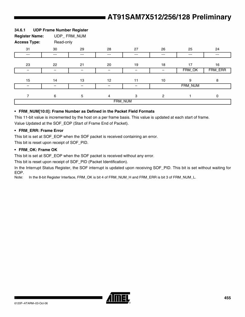
AT91SAM7X512/256/128 Preliminary
34.6.1 UDP Frame Number Register
Register Name: UDP_ FRM_NUM
Access Type: Read-only
• FRM_NUM[10:0]: Frame Number as Defined in the Packet Field Formats
This 11-bit value is incremented by the host on a per frame basis. This value is updated at each start of frame.
Value Updated at the SOF_EOP (Start of Frame End of Packet).
• FRM_ERR: Frame Error
This bit is set at SOF_EOP when the SOF packet is received containing an error.
This bit is reset upon receipt of SOF_PID.
• FRM_OK: Frame OK
This bit is set at SOF_EOP when the SOF packet is received without any error.
This bit is reset upon receipt of SOF_PID (Packet Identification).
In the Interrupt Status Register, the SOF interrupt is updated upon receiving SOF_PID. This bit is set without waiting for EOP.Note: In the 8-bit Register Interface, FRM_OK is bit 4 of FRM_NUM_H and FRM_ERR is bit 3 of FRM_NUM_L.
31 30 29 28 27 26 25 24--- --- --- --- --- --- --- ---
23 22 21 20 19 18 17 16
– – – – – – FRM_OK FRM_ERR
15 14 13 12 11 10 9 8
– – – – – FRM_NUM
7 6 5 4 3 2 1 0
FRM_NUM
4556120F–ATARM–03-Oct-06

34.6.2 UDP Global State Register
Register Name: UDP_ GLB_STAT
Access Type: Read/Write
This register is used to get and set the device state as specified in Chapter 9 of the USB Serial Bus Specification, Rev.2.0.
• FADDEN: Function Address Enable
Read:
0 = Device is not in address state.
1 = Device is in address state.
Write:
0 = No effect, only a reset can bring back a device to the default state.
1 = Sets device in address state. This occurs after a successful Set Address request. Beforehand, the UDP_ FADDR regis-ter must have been initialized with Set Address parameters. Set Address must complete the Status Stage before setting FADDEN. Refer to chapter 9 of the Universal Serial Bus Specification, Rev. 2.0 for more details.
• CONFG: Configured
Read:
0 = Device is not in configured state.
1 = Device is in configured state.
Write:
0 = Sets device in a non configured state
1 = Sets device in configured state.
The device is set in configured state when it is in address state and receives a successful Set Configuration request. Refer to Chapter 9 of the Universal Serial Bus Specification, Rev. 2.0 for more details.
31 30 29 28 27 26 25 24– – – – – – – –
23 22 21 20 19 18 17 16
– – – – – – – –
15 14 13 12 11 10 9 8
– – – – – – – –
7 6 5 4 3 2 1 0
– – – – – – CONFG FADDEN
4566120F–ATARM–03-Oct-06
AT91SAM7X512/256/128 Preliminary

AT91SAM7X512/256/128 Preliminary
34.6.3 UDP Function Address Register
Register Name: UDP_ FADDR
Access Type: Read/Write
• FADD[6:0]: Function Address Value
The Function Address Value must be programmed by firmware once the device receives a set address request from the host, and has achieved the status stage of the no-data control sequence. Refer to the Universal Serial Bus Specification, Rev. 2.0 for more information. After power up or reset, the function address value is set to 0.
• FEN: Function Enable
Read:
0 = Function endpoint disabled.
1 = Function endpoint enabled.
Write:
0 = Disables function endpoint.
1 = Default value.
The Function Enable bit (FEN) allows the microcontroller to enable or disable the function endpoints. The microcontroller sets this bit after receipt of a reset from the host. Once this bit is set, the USB device is able to accept and transfer data packets from and to the host.
31 30 29 28 27 26 25 24– – – – – – – –
23 22 21 20 19 18 17 16
– – – – – – – –
15 14 13 12 11 10 9 8
– – – – – – – FEN
7 6 5 4 3 2 1 0
– FADD
4576120F–ATARM–03-Oct-06

34.6.4 UDP Interrupt Enable Register
Register Name: UDP_ IER
Access Type: Write-only
• EP0INT: Enable Endpoint 0 Interrupt
• EP1INT: Enable Endpoint 1 Interrupt
• EP2INT: Enable Endpoint 2Interrupt
• EP3INT: Enable Endpoint 3 Interrupt
• EP4INT: Enable Endpoint 4 Interrupt
• EP5INT: Enable Endpoint 5 Interrupt
0 = No effect.
1 = Enables corresponding Endpoint Interrupt.
• RXSUSP: Enable UDP Suspend Interrupt
0 = No effect.
1 = Enables UDP Suspend Interrupt.
• RXRSM: Enable UDP Resume Interrupt
0 = No effect.
1 = Enables UDP Resume Interrupt.
• SOFINT: Enable Start Of Frame Interrupt
0 = No effect.
1 = Enables Start Of Frame Interrupt.
• WAKEUP: Enable UDP bus Wakeup Interrupt
0 = No effect.
1 = Enables USB bus Interrupt.
31 30 29 28 27 26 25 24– – – – – – – –
23 22 21 20 19 18 17 16
– – – – – – – –
15 14 13 12 11 10 9 8
– – WAKEUP – SOFINT – RXRSM RXSUSP
7 6 5 4 3 2 1 0
EP5INT EP4INT EP3INT EP2INT EP1INT EP0INT
4586120F–ATARM–03-Oct-06
AT91SAM7X512/256/128 Preliminary

AT91SAM7X512/256/128 Preliminary
34.6.5 UDP Interrupt Disable Register
Register Name: UDP_ IDR
Access Type: Write-only
• EP0INT: Disable Endpoint 0 Interrupt
• EP1INT: Disable Endpoint 1 Interrupt
• EP2INT: Disable Endpoint 2 Interrupt
• EP3INT: Disable Endpoint 3 Interrupt
• EP4INT: Disable Endpoint 4 Interrupt
• EP5INT: Disable Endpoint 5 Interrupt
0 = No effect.
1 = Disables corresponding Endpoint Interrupt.
• RXSUSP: Disable UDP Suspend Interrupt
0 = No effect.
1 = Disables UDP Suspend Interrupt.
• RXRSM: Disable UDP Resume Interrupt
0 = No effect.
1 = Disables UDP Resume Interrupt.
• SOFINT: Disable Start Of Frame Interrupt
0 = No effect.
1 = Disables Start Of Frame Interrupt
• WAKEUP: Disable USB Bus Interrupt
0 = No effect.
1 = Disables USB Bus Wakeup Interrupt.
31 30 29 28 27 26 25 24– – – – – – – –
23 22 21 20 19 18 17 16
– – – – – – – –
15 14 13 12 11 10 9 8
– – WAKEUP – SOFINT – RXRSM RXSUSP
7 6 5 4 3 2 1 0
EP5INT EP4INT EP3INT EP2INT EP1INT EP0INT
4596120F–ATARM–03-Oct-06

34.6.6 UDP Interrupt Mask Register
Register Name: UDP_ IMR
Access Type: Read-only
Note: 1. Bit 12 of UDP_IMR cannot be masked and is always read at 1.
• EP0INT: Mask Endpoint 0 Interrupt
• EP1INT: Mask Endpoint 1 Interrupt
• EP2INT: Mask Endpoint 2 Interrupt
• EP3INT: Mask Endpoint 3 Interrupt
• EP4INT: Mask Endpoint 4 Interrupt
• EP5INT: Mask Endpoint 5 Interrupt
0 = Corresponding Endpoint Interrupt is disabled.
1 = Corresponding Endpoint Interrupt is enabled.
• RXSUSP: Mask UDP Suspend Interrupt
0 = UDP Suspend Interrupt is disabled.
1 = UDP Suspend Interrupt is enabled.
• RXRSM: Mask UDP Resume Interrupt.
0 = UDP Resume Interrupt is disabled.
1 = UDP Resume Interrupt is enabled.
• SOFINT: Mask Start Of Frame Interrupt
0 = Start of Frame Interrupt is disabled.
1 = Start of Frame Interrupt is enabled.
• WAKEUP: USB Bus WAKEUP Interrupt
0 = USB Bus Wakeup Interrupt is disabled.
1 = USB Bus Wakeup Interrupt is enabled.Note: When the USB block is in suspend mode, the application may power down the USB logic. In this case, any USB HOST resume
request that is made must be taken into account and, thus, the reset value of the RXRSM bit of the register UDP_ IMR is enabled.
31 30 29 28 27 26 25 24– – – – – – – –
23 22 21 20 19 18 17 16
– – – – – – – –
15 14 13 12(1) 11 10 9 8
– – WAKEUP – SOFINT – RXRSM RXSUSP
7 6 5 4 3 2 1 0
EP5INT EP4INT EP3INT EP2INT EP1INT EP0INT
4606120F–ATARM–03-Oct-06
AT91SAM7X512/256/128 Preliminary

AT91SAM7X512/256/128 Preliminary
34.6.7 UDP Interrupt Status Register
Register Name: UDP_ ISR
Access Type: Read-only
• EP0INT: Endpoint 0 Interrupt Status
• EP1INT: Endpoint 1 Interrupt Status
• EP2INT: Endpoint 2 Interrupt Status
• EP3INT: Endpoint 3 Interrupt Status
• EP4INT: Endpoint 4 Interrupt Status
• EP5INT: Endpoint 5 Interrupt Status
0 = No Endpoint0 Interrupt pending.
1 = Endpoint0 Interrupt has been raised.
Several signals can generate this interrupt. The reason can be found by reading UDP_ CSR0:
RXSETUP set to 1
RX_DATA_BK0 set to 1
RX_DATA_BK1 set to 1
TXCOMP set to 1
STALLSENT set to 1
EP0INT is a sticky bit. Interrupt remains valid until EP0INT is cleared by writing in the corresponding UDP_ CSR0 bit.
• RXSUSP: UDP Suspend Interrupt Status
0 = No UDP Suspend Interrupt pending.
1 = UDP Suspend Interrupt has been raised.
The USB device sets this bit when it detects no activity for 3ms. The USB device enters Suspend mode.
• RXRSM: UDP Resume Interrupt Status
0 = No UDP Resume Interrupt pending.
1 =UDP Resume Interrupt has been raised.
The USB device sets this bit when a UDP resume signal is detected at its port.
After reset, the state of this bit is undefined, the application must clear this bit by setting the RXRSM flag in the UDP_ ICR register.
• SOFINT: Start of Frame Interrupt Status
0 = No Start of Frame Interrupt pending.
1 = Start of Frame Interrupt has been raised.
31 30 29 28 27 26 25 24– – – – – – – –
23 22 21 20 19 18 17 16
– – – – – – – –
15 14 13 12 11 10 9 8
– – WAKEUP ENDBUSRES SOFINT – RXRSM RXSUSP
7 6 5 4 3 2 1 0
EP5INT EP4INT EP3INT EP2INT EP1INT EP0INT
4616120F–ATARM–03-Oct-06
This interrupt is raised each time a SOF token has been detected. It can be used as a synchronization signal by using
isochronous endpoints.
• ENDBUSRES: End of BUS Reset Interrupt Status
0 = No End of Bus Reset Interrupt pending.
1 = End of Bus Reset Interrupt has been raised.
This interrupt is raised at the end of a UDP reset sequence. The USB device must prepare to receive requests on the end-point 0. The host starts the enumeration, then performs the configuration.
• WAKEUP: UDP Resume Interrupt Status
0 = No Wakeup Interrupt pending.
1 = A Wakeup Interrupt (USB Host Sent a RESUME or RESET) occurred since the last clear.
After reset the state of this bit is undefined, the application must clear this bit by setting the WAKEUP flag in the UDP_ ICR register.
4626120F–ATARM–03-Oct-06
AT91SAM7X512/256/128 Preliminary

AT91SAM7X512/256/128 Preliminary
34.6.8 UDP Interrupt Clear Register
Register Name: UDP_ ICR
Access Type: Write-only
• RXSUSP: Clear UDP Suspend Interrupt
0 = No effect.
1 = Clears UDP Suspend Interrupt.
• RXRSM: Clear UDP Resume Interrupt
0 = No effect.
1 = Clears UDP Resume Interrupt.
• SOFINT: Clear Start Of Frame Interrupt
0 = No effect.
1 = Clears Start Of Frame Interrupt.
• ENDBUSRES: Clear End of Bus Reset Interrupt
0 = No effect.
1 = Clears End of Bus Reset Interrupt.
• WAKEUP: Clear Wakeup Interrupt
0 = No effect.
1 = Clears Wakeup Interrupt.
31 30 29 28 27 26 25 24– – – – – – – –
23 22 21 20 19 18 17 16
– – – – – – – –
15 14 13 12 11 10 9 8
– – WAKEUP ENDBUSRES SOFINT – RXRSM RXSUSP
7 6 5 4 3 2 1 0
– – – – – – – –
4636120F–ATARM–03-Oct-06
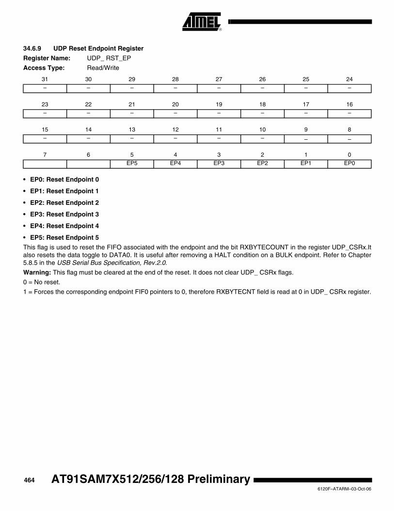
34.6.9 UDP Reset Endpoint Register
Register Name: UDP_ RST_EP
Access Type: Read/Write
• EP0: Reset Endpoint 0
• EP1: Reset Endpoint 1
• EP2: Reset Endpoint 2
• EP3: Reset Endpoint 3
• EP4: Reset Endpoint 4
• EP5: Reset Endpoint 5
This flag is used to reset the FIFO associated with the endpoint and the bit RXBYTECOUNT in the register UDP_CSRx.It also resets the data toggle to DATA0. It is useful after removing a HALT condition on a BULK endpoint. Refer to Chapter 5.8.5 in the USB Serial Bus Specification, Rev.2.0.
Warning: This flag must be cleared at the end of the reset. It does not clear UDP_ CSRx flags.
0 = No reset.
1 = Forces the corresponding endpoint FIF0 pointers to 0, therefore RXBYTECNT field is read at 0 in UDP_ CSRx register.
31 30 29 28 27 26 25 24– – – – – – – –
23 22 21 20 19 18 17 16
– – – – – – – –
15 14 13 12 11 10 9 8
– – – – – – – –
7 6 5 4 3 2 1 0
EP5 EP4 EP3 EP2 EP1 EP0
4646120F–ATARM–03-Oct-06
AT91SAM7X512/256/128 Preliminary

AT91SAM7X512/256/128 Preliminary
34.6.10 UDP Endpoint Control and Status Register
Register Name: UDP_ CSRx [x = 0..5]
Access Type: Read/Write
WARNING: Due to synchronization between MCK and UDPCK, the software application must wait for the end of the write operation before executing another write by polling the bits which must be set/cleared.
//! Clear flags of UDP UDP_CSR register and waits for synchronization #define Udp_ep_clr_flag(pInterface, endpoint, flags) \ while (pInterface->UDP_CSR[endpoint] & (flags)) \ pInterface->UDP_CSR[endpoint] &= ~(flags); \
//! Set flags of UDP UDP_CSR register and waits for synchronization #define Udp_ep_set_flag(pInterface, endpoint, flags) \ while ( (pInterface->UDP_CSR[endpoint] & (flags)) != (flags) ) \ pInterface->UDP_CSR[endpoint] |= (flags); \
• TXCOMP: Generates an IN Packet with Data Previously Written in the DPR
This flag generates an interrupt while it is set to one.
Write (Cleared by the firmware):
0 = Clear the flag, clear the interrupt.
1 = No effect.
Read (Set by the USB peripheral):
0 = Data IN transaction has not been acknowledged by the Host.
1 = Data IN transaction is achieved, acknowledged by the Host.
After having issued a Data IN transaction setting TXPKTRDY, the device firmware waits for TXCOMP to be sure that the host has acknowledged the transaction.
• RX_DATA_BK0: Receive Data Bank 0
This flag generates an interrupt while it is set to one.
Write (Cleared by the firmware):
0 = Notify USB peripheral device that data have been read in the FIFO's Bank 0.
1 = No effect.
Read (Set by the USB peripheral):
0 = No data packet has been received in the FIFO's Bank 0.
1 = A data packet has been received, it has been stored in the FIFO's Bank 0.
31 30 29 28 27 26 25 24– – – – – RXBYTECNT
23 22 21 20 19 18 17 16
RXBYTECNT
15 14 13 12 11 10 9 8
EPEDS – – – DTGLE EPTYPE
7 6 5 4 3 2 1 0
DIRRX_DATA_
BK1FORCESTALL
TXPKTRDYSTALLSENTISOERROR
RXSETUPRX_DATA_
BK0TXCOMP
4656120F–ATARM–03-Oct-06
When the device firmware has polled this bit or has been interrupted by this signal, it must transfer data from the FIFO to the microcontroller memory. The number of bytes received is available in RXBYTCENT field. Bank 0 FIFO values are read through the UDP_ FDRx register. Once a transfer is done, the device firmware must release Bank 0 to the USB peripheral device by clearing RX_DATA_BK0.
• RXSETUP: Received Setup
This flag generates an interrupt while it is set to one.
Read:
0 = No setup packet available.
1 = A setup data packet has been sent by the host and is available in the FIFO.
Write:
0 = Device firmware notifies the USB peripheral device that it has read the setup data in the FIFO.
1 = No effect.
This flag is used to notify the USB device firmware that a valid Setup data packet has been sent by the host and success-fully received by the USB device. The USB device firmware may transfer Setup data from the FIFO by reading the UDP_ FDRx register to the microcontroller memory. Once a transfer has been done, RXSETUP must be cleared by the device firmware.
Ensuing Data OUT transaction is not accepted while RXSETUP is set.
• STALLSENT: Stall Sent (Control, Bulk Interrupt Endpoints) / ISOERROR (Isochronous Endpoints)
This flag generates an interrupt while it is set to one.
STALLSENT: This ends a STALL handshake.
Read:
0 = The host has not acknowledged a STALL.
1 = Host has acknowledged the stall.
Write:
0 = Resets the STALLSENT flag, clears the interrupt.
1 = No effect.
This is mandatory for the device firmware to clear this flag. Otherwise the interrupt remains.
Refer to chapters 8.4.5 and 9.4.5 of the Universal Serial Bus Specification, Rev. 2.0 for more information on the STALL handshake.
ISOERROR: A CRC error has been detected in an isochronous transfer.
Read:
0 = No error in the previous isochronous transfer.
1 = CRC error has been detected, data available in the FIFO are corrupted.
Write:
0 = Resets the ISOERROR flag, clears the interrupt.
1 = No effect.
• TXPKTRDY: Transmit Packet Ready
This flag is cleared by the USB device.
This flag is set by the USB device firmware.
Read:
0 = Can be set to one to send the FIFO data.
1 = The data is waiting to be sent upon reception of token IN.
4666120F–ATARM–03-Oct-06
AT91SAM7X512/256/128 Preliminary

AT91SAM7X512/256/128 Preliminary
Write:
0 = No effect.
1 = A new data payload is has been written in the FIFO by the firmware and is ready to be sent.
This flag is used to generate a Data IN transaction (device to host). Device firmware checks that it can write a data payload in the FIFO, checking that TXPKTRDY is cleared. Transfer to the FIFO is done by writing in the UDP_ FDRx register. Once the data payload has been transferred to the FIFO, the firmware notifies the USB device setting TXPKTRDY to one. USB bus transactions can start. TXCOMP is set once the data payload has been received by the host.
• FORCESTALL: Force Stall (used by Control, Bulk and Isochronous Endpoints)
Read:
0 = Normal state.
1 = Stall state.
Write:
0 = Return to normal state.
1 = Send STALL to the host.
Refer to chapters 8.4.5 and 9.4.5 of the Universal Serial Bus Specification, Rev. 2.0 for more information on the STALL handshake.
Control endpoints: During the data stage and status stage, this bit indicates that the microcontroller cannot complete the request.
Bulk and interrupt endpoints: This bit notifies the host that the endpoint is halted.
The host acknowledges the STALL, device firmware is notified by the STALLSENT flag.
• RX_DATA_BK1: Receive Data Bank 1 (only used by endpoints with ping-pong attributes)
This flag generates an interrupt while it is set to one.
Write (Cleared by the firmware):
0 = Notifies USB device that data have been read in the FIFO’s Bank 1.
1 = No effect.
Read (Set by the USB peripheral):
0 = No data packet has been received in the FIFO's Bank 1.
1 = A data packet has been received, it has been stored in FIFO's Bank 1.
When the device firmware has polled this bit or has been interrupted by this signal, it must transfer data from the FIFO to microcontroller memory. The number of bytes received is available in RXBYTECNT field. Bank 1 FIFO values are read through UDP_ FDRx register. Once a transfer is done, the device firmware must release Bank 1 to the USB device by clearing RX_DATA_BK1.
• DIR: Transfer Direction (only available for control endpoints)
Read/Write
0 = Allows Data OUT transactions in the control data stage.
1 = Enables Data IN transactions in the control data stage.
Refer to Chapter 8.5.3 of the Universal Serial Bus Specification, Rev. 2.0 for more information on the control data stage.
This bit must be set before UDP_ CSRx/RXSETUP is cleared at the end of the setup stage. According to the request sent in the setup data packet, the data stage is either a device to host (DIR = 1) or host to device (DIR = 0) data transfer. It is not necessary to check this bit to reverse direction for the status stage.
4676120F–ATARM–03-Oct-06

• EPTYPE[2:0]: Endpoint Type
• DTGLE: Data Toggle
Read-only
0 = Identifies DATA0 packet.
1 = Identifies DATA1 packet.
Refer to Chapter 8 of the Universal Serial Bus Specification, Rev. 2.0 for more information on DATA0, DATA1 packet definitions.
• EPEDS: Endpoint Enable Disable
Read:
0 = Endpoint disabled.
1 = Endpoint enabled.
Write:
0 = Disables endpoint.
1 = Enables endpoint.
• RXBYTECNT[10:0]: Number of Bytes Available in the FIFO
Read-only
When the host sends a data packet to the device, the USB device stores the data in the FIFO and notifies the microcontrol-ler. The microcontroller can load the data from the FIFO by reading RXBYTECENT bytes in the UDP_ FDRx register.
Read/Write
000 Control
001 Isochronous OUT
101 Isochronous IN
010 Bulk OUT
110 Bulk IN
011 Interrupt OUT
111 Interrupt IN
4686120F–ATARM–03-Oct-06
AT91SAM7X512/256/128 Preliminary
AT91SAM7X512/256/128 Preliminary
34.6.11 UDP FIFO Data Register
Register Name: UDP_ FDRx [x = 0..5]
Access Type: Read/Write
• FIFO_DATA[7:0]: FIFO Data Value
The microcontroller can push or pop values in the FIFO through this register.
RXBYTECNT in the corresponding UDP_ CSRx register is the number of bytes to be read from the FIFO (sent by the host).
The maximum number of bytes to write is fixed by the Max Packet Size in the Standard Endpoint Descriptor. It can not be more than the physical memory size associated to the endpoint. Refer to the Universal Serial Bus Specification, Rev. 2.0for more information.
31 30 29 28 27 26 25 24– – – – – – – –
23 22 21 20 19 18 17 16
– – – – – – – –
15 14 13 12 11 10 9 8
– – – – – – – –
7 6 5 4 3 2 1 0
FIFO_DATA
4696120F–ATARM–03-Oct-06

34.6.12 UDP Transceiver Control Register
Register Name: UDP_ TXVC
Access Type: Read/Write
WARNING: The UDP peripheral clock in the Power Management Controller (PMC) must be enabled before any read/write operations to the UDP registers including the UDP_TXCV register.
• TXVDIS: Transceiver Disable
When UDP is disabled, power consumption can be reduced significantly by disabling the embedded transceiver. This can be done by setting TXVDIS field.
To enable the transceiver, TXVDIS must be cleared.
NOTE: If the USB pullup is not connected on DP, the user should not write in any UDP register other than the UDP_ TXVC register. This is because if DP and DM are floating at 0, or pulled down, then SE0 is received by the device with the conse-quence of a USB Reset.
31 30 29 28 27 26 25 24– – – – – – – –
23 22 21 20 19 18 17 16
– – – – – – – –
15 14 13 12 11 10 9 8
– – – – – – – TXVDIS
7 6 5 4 3 2 1 0
– – – – – – – –
4706120F–ATARM–03-Oct-06
AT91SAM7X512/256/128 Preliminary

AT91SAM7X512/256/128 Preliminary
35. Analog-to-Digital Converter (ADC)
35.1 Overview
The ADC is based on a Successive Approximation Register (SAR) 10-bit Analog-to-Digital Con-verter (ADC). It also integrates an 8-to-1 analog multiplexer, making possible the analog-to-digital conversions of 8 analog lines. The conversions extend from 0V to ADVREF.
The ADC supports an 8-bit or 10-bit resolution mode, and conversion results are reported in a common register for all channels, as well as in a channel-dedicated register. Software trigger, external trigger on rising edge of the ADTRG pin or internal triggers from Timer Counter out-put(s) are configurable.
The ADC also integrates a Sleep Mode and a conversion sequencer and connects with a PDC channel. These features reduce both power consumption and processor intervention.
Finally, the user can configure ADC timings, such as Startup Time and Sample & Hold Time.
35.2 Block Diagram
Figure 35-1. Analog-to-Digital Converter Block Diagram
ADC Interrupt
ADC
ADTRG
VDDANA
ADVREF
GND
Trigger Selection
Control Logic
SuccessiveApproximation
RegisterAnalog-to-Digital
Converter
Timer Counter
Channels
UserInterface
AIC
Peripheral Bridge
APB
PDC
ASB
Dedicated AnalogInputs
Analog InputsMultiplexed
with I/O lines
AD-
AD-
AD-
PIOAD-
AD-
AD-
4716120F–ATARM–03-Oct-06
35.3 Signal Description
Table 35-1. ADC Pin Description
Pin Name Description
VDDANA Analog power supply
ADVREF Reference voltage
AD0 - AD7 Analog input channels
ADTRG External trigger
4726120F–ATARM–03-Oct-06
AT91SAM7X512/256/128 Preliminary

AT91SAM7X512/256/128 Preliminary
35.4 Product Dependencies
35.4.1 Power Management
The ADC is automatically clocked after the first conversion in Normal Mode. In Sleep Mode, the ADC clock is automatically stopped after each conversion. As the logic is small and the ADC cell can be put into Sleep Mode, the Power Management Controller has no effect on the ADC behavior.
35.4.2 Interrupt Sources
The ADC interrupt line is connected on one of the internal sources of the Advanced Interrupt Controller. Using the ADC interrupt requires the AIC to be programmed first.
35.4.3 Analog Inputs
The analog input pins can be multiplexed with PIO lines. In this case, the assignment of the ADC input is automatically done as soon as the corresponding channel is enabled by writing the reg-ister ADC_CHER. By default, after reset, the PIO line is configured as input with its pull-up enabled and the ADC input is connected to the GND.
35.4.4 I/O Lines
The pin ADTRG may be shared with other peripheral functions through the PIO Controller. In this case, the PIO Controller should be set accordingly to assign the pin ADTRG to the ADC function.
35.4.5 Timer Triggers
Timer Counters may or may not be used as hardware triggers depending on user requirements. Thus, some or all of the timer counters may be non-connected.
35.4.6 Conversion Performances
For performance and electrical characteristics of the ADC, see the DC Characteristics section.
4736120F–ATARM–03-Oct-06
35.5 Functional Description
35.5.1 Analog-to-digital Conversion
The ADC uses the ADC Clock to perform conversions. Converting a single analog value to a 10-bit digital data requires Sample and Hold Clock cycles as defined in the field SHTIM of the ”ADC Mode Register” on page 481 and 10 ADC Clock cycles. The ADC Clock frequency is selected in the PRESCAL field of the Mode Register (ADC_MR).
The ADC clock range is between MCK/2, if PRESCAL is 0, and MCK/128, if PRESCAL is set to 63 (0x3F). PRESCAL must be programmed in order to provide an ADC clock frequency accord-ing to the parameters given in the Product definition section.
35.5.2 Conversion Reference
The conversion is performed on a full range between 0V and the reference voltage pin ADVREF. Analog inputs between these voltages convert to values based on a linear conversion.
35.5.3 Conversion Resolution
The ADC supports 8-bit or 10-bit resolutions. The 8-bit selection is performed by setting the bit LOWRES in the ADC Mode Register (ADC_MR). By default, after a reset, the resolution is the highest and the DATA field in the data registers is fully used. By setting the bit LOWRES, the ADC switches in the lowest resolution and the conversion results can be read in the eight lowest significant bits of the data registers. The two highest bits of the DATA field in the corresponding ADC_CDR register and of the LDATA field in the ADC_LCDR register read 0.
Moreover, when a PDC channel is connected to the ADC, 10-bit resolution sets the transfer request sizes to 16-bit. Setting the bit LOWRES automatically switches to 8-bit data transfers. In this case, the destination buffers are optimized.
4746120F–ATARM–03-Oct-06
AT91SAM7X512/256/128 Preliminary
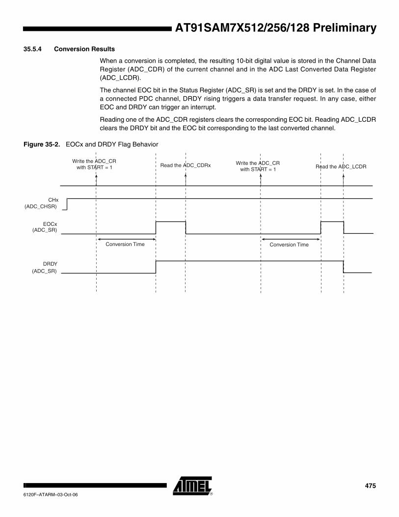
AT91SAM7X512/256/128 Preliminary
35.5.4 Conversion Results
When a conversion is completed, the resulting 10-bit digital value is stored in the Channel Data Register (ADC_CDR) of the current channel and in the ADC Last Converted Data Register (ADC_LCDR).
The channel EOC bit in the Status Register (ADC_SR) is set and the DRDY is set. In the case of a connected PDC channel, DRDY rising triggers a data transfer request. In any case, either EOC and DRDY can trigger an interrupt.
Reading one of the ADC_CDR registers clears the corresponding EOC bit. Reading ADC_LCDR clears the DRDY bit and the EOC bit corresponding to the last converted channel.
Figure 35-2. EOCx and DRDY Flag Behavior
Conversion Time
Read the ADC_CDRx
EOCx
DRDY
Read the ADC_LCDR
CHx(ADC_CHSR)
(ADC_SR)
(ADC_SR)
Write the ADC_CR with START = 1
Conversion Time
Write the ADC_CR with START = 1
4756120F–ATARM–03-Oct-06

If the ADC_CDR is not read before further incoming data is converted, the corresponding Over-run Error (OVRE) flag is set in the Status Register (ADC_SR).
In the same way, new data converted when DRDY is high sets the bit GOVRE (General Overrun Error) in ADC_SR.
The OVRE and GOVRE flags are automatically cleared when ADC_SR is read.
Figure 35-3. GOVRE and OVREx Flag Behavior
Warning: If the corresponding channel is disabled during a conversion or if it is disabled and then reenabled during a conversion, its associated data and its corresponding EOC and OVRE flags in ADC_SR are unpredictable.
EOC0
GOVRE
CH0(ADC_CHSR)
(ADC_SR)
(ADC_SR)
ADTRG
EOC1
CH1(ADC_CHSR)
(ADC_SR)
OVRE0(ADC_SR)
Undefined Data Data A Data BADC_LCDR
Undefined Data Data AADC_CDR0
Undefined Data Data BADC_CDR1
Data C
Data C
ConversionConversion
Read ADC_SR
DRDY(ADC_SR)
Read ADC_CDR1
Read ADC_CDR0
Conversion
4766120F–ATARM–03-Oct-06
AT91SAM7X512/256/128 Preliminary

AT91SAM7X512/256/128 Preliminary
35.5.5 Conversion Triggers
Conversions of the active analog channels are started with a software or a hardware trigger. The software trigger is provided by writing the Control Register (ADC_CR) with the bit START at 1.
The hardware trigger can be one of the TIOA outputs of the Timer Counter channels, or the external trigger input of the ADC (ADTRG). The hardware trigger is selected with the field TRG-SEL in the Mode Register (ADC_MR). The selected hardware trigger is enabled with the bit TRGEN in the Mode Register (ADC_MR).
If a hardware trigger is selected, the start of a conversion is detected at each rising edge of the selected signal. If one of the TIOA outputs is selected, the corresponding Timer Counter channel must be programmed in Waveform Mode.
Only one start command is necessary to initiate a conversion sequence on all the channels. The ADC hardware logic automatically performs the conversions on the active channels, then waits for a new request. The Channel Enable (ADC_CHER) and Channel Disable (ADC_CHDR) Reg-isters enable the analog channels to be enabled or disabled independently.
If the ADC is used with a PDC, only the transfers of converted data from enabled channels are performed and the resulting data buffers should be interpreted accordingly.
Warning: Enabling hardware triggers does not disable the software trigger functionality. Thus, if a hardware trigger is selected, the start of a conversion can be initiated either by the hardware or the software trigger.
35.5.6 Sleep Mode and Conversion Sequencer
The ADC Sleep Mode maximizes power saving by automatically deactivating the ADC when it is not being used for conversions. Sleep Mode is selected by setting the bit SLEEP in the Mode Register ADC_MR.
The SLEEP mode is automatically managed by a conversion sequencer, which can automati-cally process the conversions of all channels at lowest power consumption.
When a start conversion request occurs, the ADC is automatically activated. As the analog cell requires a start-up time, the logic waits during this time and starts the conversion on the enabled channels. When all conversions are complete, the ADC is deactivated until the next trigger. Trig-gers occurring during the sequence are not taken into account.
The conversion sequencer allows automatic processing with minimum processor intervention and optimized power consumption. Conversion sequences can be performed periodically using a Timer/Counter output. The periodic acquisition of several samples can be processed automat-ically without any intervention of the processor thanks to the PDC.
Note: The reference voltage pins always remain connected in normal mode as in sleep mode.
4776120F–ATARM–03-Oct-06
35.5.7 ADC Timings
Each ADC has its own minimal Startup Time that is programmed through the field STARTUP in the Mode Register ADC_MR.
In the same way, a minimal Sample and Hold Time is necessary for the ADC to guarantee the best converted final value between two channels selection. This time has to be programmed through the bitfield SHTIM in the Mode Register ADC_MR.
Warning: No input buffer amplifier to isolate the source is included in the ADC. This must be taken into consideration to program a precise value in the SHTIM field. See the section ADC Characteristics in the product datasheet.
4786120F–ATARM–03-Oct-06
AT91SAM7X512/256/128 Preliminary

AT91SAM7X512/256/128 Preliminary
35.6 Analog-to-digital Converter (ADC) User Interface
Table 35-2. ADC Register Mapping
Offset Register Name Access Reset State
0x00 Control Register ADC_CR Write-only –
0x04 Mode Register ADC_MR Read/Write 0x00000000
0x08 Reserved – – –
0x0C Reserved – – –
0x10 Channel Enable Register ADC_CHER Write-only –
0x14 Channel Disable Register ADC_CHDR Write-only –
0x18 Channel Status Register ADC_CHSR Read-only 0x00000000
0x1C Status Register ADC_SR Read-only 0x000C0000
0x20 Last Converted Data Register ADC_LCDR Read-only 0x00000000
0x24 Interrupt Enable Register ADC_IER Write-only –
0x28 Interrupt Disable Register ADC_IDR Write-only –
0x2C Interrupt Mask Register ADC_IMR Read-only 0x00000000
0x30 Channel Data Register 0 ADC_CDR0 Read-only 0x00000000
0x34 Channel Data Register 1 ADC_CDR1 Read-only 0x00000000
... ... ... ... ...
0x4C Channel Data Register 7 ADC_CDR7 Read-only 0x00000000
0x50 - 0xFC Reserved – – –
4796120F–ATARM–03-Oct-06

35.6.1 ADC Control Register
Register Name: ADC_CR
Access Type: Write-only
• SWRST: Software Reset
0 = No effect.
1 = Resets the ADC simulating a hardware reset.
• START: Start Conversion
0 = No effect.
1 = Begins analog-to-digital conversion.
31 30 29 28 27 26 25 24
– – – – – – – –
23 22 21 20 19 18 17 16
– – – – – – – –
15 14 13 12 11 10 9 8
– – – – – – – –
7 6 5 4 3 2 1 0
– – – – – – START SWRST
4806120F–ATARM–03-Oct-06
AT91SAM7X512/256/128 Preliminary
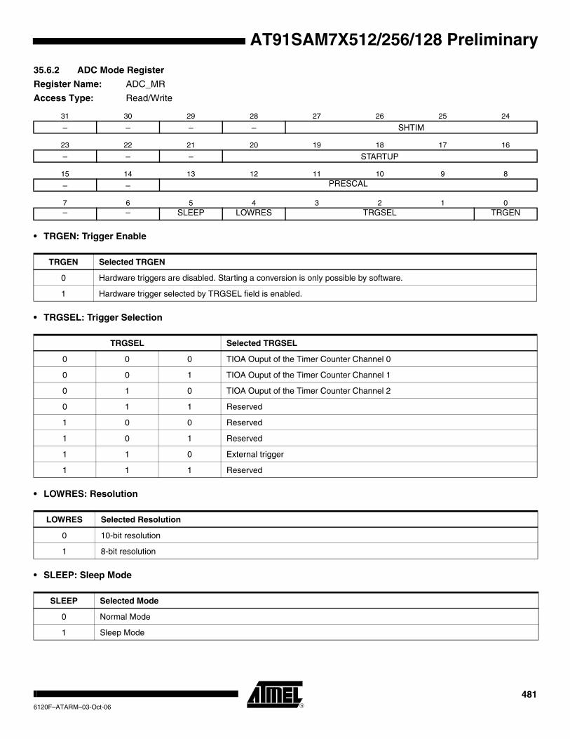
AT91SAM7X512/256/128 Preliminary
35.6.2 ADC Mode Register
Register Name: ADC_MR
Access Type: Read/Write
• TRGEN: Trigger Enable
• TRGSEL: Trigger Selection
• LOWRES: Resolution
• SLEEP: Sleep Mode
31 30 29 28 27 26 25 24
– – – – SHTIM
23 22 21 20 19 18 17 16
– – – STARTUP
15 14 13 12 11 10 9 8
– – PRESCAL
7 6 5 4 3 2 1 0– – SLEEP LOWRES TRGSEL TRGEN
TRGEN Selected TRGEN
0 Hardware triggers are disabled. Starting a conversion is only possible by software.
1 Hardware trigger selected by TRGSEL field is enabled.
TRGSEL Selected TRGSEL
0 0 0 TIOA Ouput of the Timer Counter Channel 0
0 0 1 TIOA Ouput of the Timer Counter Channel 1
0 1 0 TIOA Ouput of the Timer Counter Channel 2
0 1 1 Reserved
1 0 0 Reserved
1 0 1 Reserved
1 1 0 External trigger
1 1 1 Reserved
LOWRES Selected Resolution
0 10-bit resolution
1 8-bit resolution
SLEEP Selected Mode
0 Normal Mode
1 Sleep Mode
4816120F–ATARM–03-Oct-06

• PRESCAL: Prescaler Rate Selection ADCClock = MCK / ( (PRESCAL+1) * 2 )
• STARTUP: Start Up TimeStartup Time = (STARTUP+1) * 8 / ADCClock
• SHTIM: Sample & Hold TimeSample & Hold Time = (SHTIM+1) / ADCClock
4826120F–ATARM–03-Oct-06
AT91SAM7X512/256/128 Preliminary
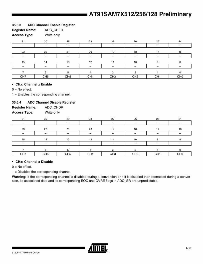
AT91SAM7X512/256/128 Preliminary
35.6.3 ADC Channel Enable Register
Register Name: ADC_CHER
Access Type: Write-only
• CHx: Channel x Enable
0 = No effect.
1 = Enables the corresponding channel.
35.6.4 ADC Channel Disable Register
Register Name: ADC_CHDR
Access Type: Write-only
• CHx: Channel x Disable
0 = No effect.
1 = Disables the corresponding channel.
Warning: If the corresponding channel is disabled during a conversion or if it is disabled then reenabled during a conver-sion, its associated data and its corresponding EOC and OVRE flags in ADC_SR are unpredictable.
31 30 29 28 27 26 25 24
– – – – – – – –
23 22 21 20 19 18 17 16
– – – – – – – –
15 14 13 12 11 10 9 8
– – – – – – – –
7 6 5 4 3 2 1 0
CH7 CH6 CH5 CH4 CH3 CH2 CH1 CH0
31 30 29 28 27 26 25 24
– – – – – – – –
23 22 21 20 19 18 17 16
– – – – – – – –
15 14 13 12 11 10 9 8
– – – – – – – –
7 6 5 4 3 2 1 0
CH7 CH6 CH5 CH4 CH3 CH2 CH1 CH0
4836120F–ATARM–03-Oct-06

35.6.5 ADC Channel Status Register
Register Name: ADC_CHSR
Access Type: Read-only
• CHx: Channel x Status
0 = Corresponding channel is disabled.
1 = Corresponding channel is enabled.
31 30 29 28 27 26 25 24
– – – – – – – –
23 22 21 20 19 18 17 16
– – – – – – – –
15 14 13 12 11 10 9 8
– – – – – – – –
7 6 5 4 3 2 1 0
CH7 CH6 CH5 CH4 CH3 CH2 CH1 CH0
4846120F–ATARM–03-Oct-06
AT91SAM7X512/256/128 Preliminary

AT91SAM7X512/256/128 Preliminary
35.6.6 ADC Status Register
Register Name: ADC_SR
Access Type: Read-only
• EOCx: End of Conversion x
0 = Corresponding analog channel is disabled, or the conversion is not finished.
1 = Corresponding analog channel is enabled and conversion is complete.
• OVREx: Overrun Error x
0 = No overrun error on the corresponding channel since the last read of ADC_SR.
1 = There has been an overrun error on the corresponding channel since the last read of ADC_SR.
• DRDY: Data Ready
0 = No data has been converted since the last read of ADC_LCDR.
1 = At least one data has been converted and is available in ADC_LCDR.
• GOVRE: General Overrun Error
0 = No General Overrun Error occurred since the last read of ADC_SR.
1 = At least one General Overrun Error has occurred since the last read of ADC_SR.
• ENDRX: End of RX Buffer
0 = The Receive Counter Register has not reached 0 since the last write in ADC_RCR or ADC_RNCR.
1 = The Receive Counter Register has reached 0 since the last write in ADC_RCR or ADC_RNCR.
• RXBUFF: RX Buffer Full
0 = ADC_RCR or ADC_RNCR have a value other than 0.
1 = Both ADC_RCR and ADC_RNCR have a value of 0.
31 30 29 28 27 26 25 24
– – – – – – – –
23 22 21 20 19 18 17 16
– – – – RXBUFF ENDRX GOVRE DRDY
15 14 13 12 11 10 9 8
OVRE7 OVRE6 OVRE5 OVRE4 OVRE3 OVRE2 OVRE1 OVRE0
7 6 5 4 3 2 1 0
EOC7 EOC6 EOC5 EOC4 EOC3 EOC2 EOC1 EOC0
4856120F–ATARM–03-Oct-06

35.6.7 ADC Last Converted Data Register
Register Name: ADC_LCDR
Access Type: Read-only
• LDATA: Last Data Converted
The analog-to-digital conversion data is placed into this register at the end of a conversion and remains until a new conver-sion is completed.
31 30 29 28 27 26 25 24
– – – – – – – –
23 22 21 20 19 18 17 16
– – – – – – – –
15 14 13 12 11 10 9 8
– – – – – – LDATA
7 6 5 4 3 2 1 0LDATA
4866120F–ATARM–03-Oct-06
AT91SAM7X512/256/128 Preliminary
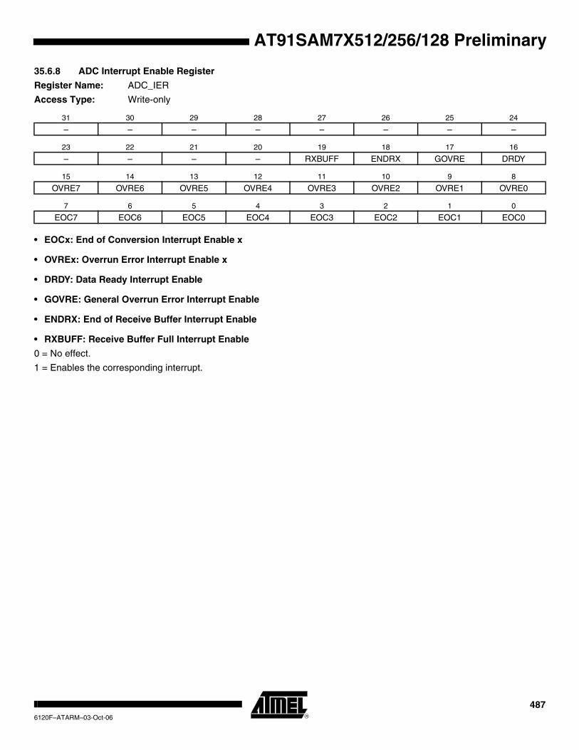
AT91SAM7X512/256/128 Preliminary
35.6.8 ADC Interrupt Enable Register
Register Name: ADC_IER
Access Type: Write-only
• EOCx: End of Conversion Interrupt Enable x
• OVREx: Overrun Error Interrupt Enable x
• DRDY: Data Ready Interrupt Enable
• GOVRE: General Overrun Error Interrupt Enable
• ENDRX: End of Receive Buffer Interrupt Enable
• RXBUFF: Receive Buffer Full Interrupt Enable
0 = No effect.
1 = Enables the corresponding interrupt.
31 30 29 28 27 26 25 24
– – – – – – – –
23 22 21 20 19 18 17 16
– – – – RXBUFF ENDRX GOVRE DRDY
15 14 13 12 11 10 9 8
OVRE7 OVRE6 OVRE5 OVRE4 OVRE3 OVRE2 OVRE1 OVRE0
7 6 5 4 3 2 1 0
EOC7 EOC6 EOC5 EOC4 EOC3 EOC2 EOC1 EOC0
4876120F–ATARM–03-Oct-06

35.6.9 ADC Interrupt Disable Register
Register Name: ADC_IDR
Access Type: Write-only
• EOCx: End of Conversion Interrupt Disable x
• OVREx: Overrun Error Interrupt Disable x
• DRDY: Data Ready Interrupt Disable
• GOVRE: General Overrun Error Interrupt Disable
• ENDRX: End of Receive Buffer Interrupt Disable
• RXBUFF: Receive Buffer Full Interrupt Disable
0 = No effect.
1 = Disables the corresponding interrupt.
31 30 29 28 27 26 25 24
– – – – – – – –
23 22 21 20 19 18 17 16
– – – – RXBUFF ENDRX GOVRE DRDY
15 14 13 12 11 10 9 8
OVRE7 OVRE6 OVRE5 OVRE4 OVRE3 OVRE2 OVRE1 OVRE0
7 6 5 4 3 2 1 0
EOC7 EOC6 EOC5 EOC4 EOC3 EOC2 EOC1 EOC0
4886120F–ATARM–03-Oct-06
AT91SAM7X512/256/128 Preliminary

AT91SAM7X512/256/128 Preliminary
35.6.10 ADC Interrupt Mask Register
Register Name: ADC_IMR
Access Type: Read-only
• EOCx: End of Conversion Interrupt Mask x
• OVREx: Overrun Error Interrupt Mask x
• DRDY: Data Ready Interrupt Mask
• GOVRE: General Overrun Error Interrupt Mask
• ENDRX: End of Receive Buffer Interrupt Mask
• RXBUFF: Receive Buffer Full Interrupt Mask
0 = The corresponding interrupt is disabled.
1 = The corresponding interrupt is enabled.
31 30 29 28 27 26 25 24
– – – – – – – –
23 22 21 20 19 18 17 16
– – – – RXBUFF ENDRX GOVRE DRDY
15 14 13 12 11 10 9 8
OVRE7 OVRE6 OVRE5 OVRE4 OVRE3 OVRE2 OVRE1 OVRE0
7 6 5 4 3 2 1 0
EOC7 EOC6 EOC5 EOC4 EOC3 EOC2 EOC1 EOC0
4896120F–ATARM–03-Oct-06

35.6.11 ADC Channel Data Register
Register Name: ADC_CDRx
Access Type: Read-only
• DATA: Converted Data
The analog-to-digital conversion data is placed into this register at the end of a conversion and remains until a new conver-sion is completed. The Convert Data Register (CDR) is only loaded if the corresponding analog channel is enabled.
31 30 29 28 27 26 25 24
– – – – – – – –
23 22 21 20 19 18 17 16
– – – – – – – –
15 14 13 12 11 10 9 8
– – – – – – DATA
7 6 5 4 3 2 1 0DATA
4906120F–ATARM–03-Oct-06
AT91SAM7X512/256/128 Preliminary
AT91SAM7X512/256/128 Preliminary
36. Controller Area Network (CAN)
36.1 DescriptionThe CAN controller provides all the features required to implement the serial communication protocol CAN defined by Robert Bosch GmbH, the CAN specification as referred to by ISO/11898A (2.0 Part A and 2.0 Part B) for high speeds and ISO/11519-2 for low speeds. The CAN Controller is able to handle all types of frames (Data, Remote, Error and Overload) and achieves a bitrate of 1 Mbit/sec.
CAN controller accesses are made through configuration registers. 8 independent message objects (mailboxes) are implemented.
Any mailbox can be programmed as a reception buffer block (even non-consecutive buffers). For the reception of defined messages, one or several message objects can be masked with-out participating in the buffer feature. An interrupt is generated when the buffer is full. According to the mailbox configuration, the first message received can be locked in the CAN controller registers until the application acknowledges it, or this message can be discarded by new received messages.
Any mailbox can be programmed for transmission. Several transmission mailboxes can be enabled in the same time. A priority can be defined for each mailbox independently.
An internal 16-bit timer is used to stamp each received and sent message. This timer starts counting as soon as the CAN controller is enabled. This counter can be reset by the applica-tion or automatically after a reception in the last mailbox in Time Triggered Mode.
The CAN controller offers optimized features to support the Time Triggered Communication (TTC) protocol.
4916120F–ATARM–03-Oct-06
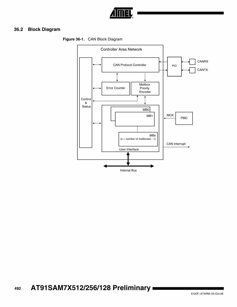
36.2 Block Diagram
Figure 36-1. CAN Block Diagram
Internal Bus
CAN Interrupt
CANRX
Controller Area Network
PIO
CANTX
Error Counter
User Interface
PMCMCK
Mailbox Priority Encoder
MB0
MBx(x = number of mailboxes - 1)
Control &
Status
CAN Protocol Controller
MB1
4926120F–ATARM–03-Oct-06
AT91SAM7X512/256/128 Preliminary

AT91SAM7X512/256/128 Preliminary
36.3 Application Block Diagram
Figure 36-2. Application Block Diagram
36.4 I/O Lines Description
36.5 Product Dependencies
36.5.1 I/O LinesThe pins used for interfacing the CAN may be multiplexed with the PIO lines. The programmer must first program the PIO controller to assign the desired CAN pins to their peripheral func-tion. If I/O lines of the CAN are not used by the application, they can be used for other purposes by the PIO Controller.
36.5.2 Power ManagementThe programmer must first enable the CAN clock in the Power Management Controller (PMC) before using the CAN.
A Low-power Mode is defined for the CAN controller: If the application does not require CAN operations, the CAN clock can be stopped when not needed and be restarted later. Before stopping the clock, the CAN Controller must be in Low-power Mode to complete the current transfer. After restarting the clock, the application must disable the Low-power Mode of the CAN controller.
36.5.3 Interrupt The CAN interrupt line is connected on one of the internal sources of the Advanced Interrupt Controller. Using the CAN interrupt requires the AIC to be programmed first. Note that it is not recommended to use the CAN interrupt line in edge-sensitive mode.
Software
Software
CAN Controller
Transceiver
ImplementationLayers
CAN-based Application Layer
CAN-based Profiles
CAN Data Link Layer
CAN Physical Layer
Table 36-1. I/O Lines Description
Name Description Type
CANRX CAN Receive Serial Data Input
CANTX CAN Transmit Serial Data Output
4936120F–ATARM–03-Oct-06

AT91SAM7X512/256/128 Preliminary
36.6 CAN Controller Features
36.6.1 CAN Protocol OverviewThe Controller Area Network (CAN) is a multi-master serial communication protocol that effi-ciently supports real-time control with a very high level of security with bit rates up to 1 Mbit/s.
The CAN protocol supports four different frame types:
• Data frames: They carry data from a transmitter node to the receiver nodes. The overall maximum data frame length is 108 bits for a standard frame and 128 bits for an extended frame.
• Remote frames: A destination node can request data from the source by sending a remote frame with an identifier that matches the identifier of the required data frame. The appropriate data source node then sends a data frame as a response to this node request.
• Error frames: An error frame is generated by any node that detects a bus error.
• Overload frames: They provide an extra delay between the preceding and the successive data frames or remote frames.
The Atmel CAN controller provides the CPU with full functionality of the CAN protocol V2.0 Part A and V2.0 Part B. It minimizes the CPU load in communication overhead. The Data Link Layer and part of the physical layer are automatically handled by the CAN controller itself.
The CPU reads or writes data or messages via the CAN controller mailboxes. An identifier is assigned to each mailbox. The CAN controller encapsulates or decodes data messages to build or to decode bus data frames. Remote frames, error frames and overload frames are automatically handled by the CAN controller under supervision of the software application.
36.6.2 Mailbox OrganizationThe CAN module has 8 buffers, also called channels or mailboxes. An identifier that corre-sponds to the CAN identifier is defined for each active mailbox. Message identifiers can match the standard frame identifier or the extended frame identifier. This identifier is defined for the first time during the CAN initialization, but can be dynamically reconfigured later so that the mailbox can handle a new message family. Several mailboxes can be configured with the same ID.
Each mailbox can be configured in receive or in transmit mode independently. The mailbox object type is defined in the MOT field of the CAN_MMRx register.
36.6.2.1 Message Acceptance ProcedureIf the MIDE field in the CAN_MIDx register is set, the mailbox can handle the extended format identifier; otherwise, the mailbox handles the standard format identifier. Once a new message is received, its ID is masked with the CAN_MAMx value and compared with the CAN_MIDx value. If accepted, the message ID is copied to the CAN_MIDx register.
4946120F–ATARM–03-Oct-06

AT91SAM7X512/256/128 Preliminary
Figure 36-3. Message Acceptance Procedure
If a mailbox is dedicated to receiving several messages (a family of messages) with different IDs, the acceptance mask defined in the CAN_MAMx register must mask the variable part of the ID family. Once a message is received, the application must decode the masked bits in the CAN_MIDx. To speed up the decoding, masked bits are grouped in the family ID register (CAN_MFIDx).
For example, if the following message IDs are handled by the same mailbox:
ID0 101000100100010010000100 0 11 00b
ID1 101000100100010010000100 0 11 01b
ID2 101000100100010010000100 0 11 10b
ID3 101000100100010010000100 0 11 11b
ID4 101000100100010010000100 1 11 00b
ID5 101000100100010010000100 1 11 01b
ID6 101000100100010010000100 1 11 10b
ID7 101000100100010010000100 1 11 11b
The CAN_MIDx and CAN_MAMx of Mailbox x must be initialized to the corresponding values:
CAN_MIDx = 001 101000100100010010000100 x 11 xxb
CAN_MAMx = 001 111111111111111111111111 0 11 00b
If Mailbox x receives a message with ID6, then CAN_MIDx and CAN_MFIDx are set:
CAN_MIDx = 001 101000100100010010000100 1 11 10b
CAN_MFIDx = 00000000000000000000000000000110b
If the application associates a handler for each message ID, it may define an array of pointers to functions:
void (*pHandler[8])(void);
When a message is received, the corresponding handler can be invoked using CAN_MFIDx register and there is no need to check masked bits:
unsigned int MFID0_register;
MFID0_register = Get_CAN_MFID0_Register();
// Get_CAN_MFID0_Register() returns the value of the CAN_MFID0 register
pHandler[MFID0_register]();
CAN_MIDx CAN_MAMx Message Received
& &
==
Message Accepted
Message RefusedNo
Yes
CAN_MFIDx
4956120F–ATARM–03-Oct-06
AT91SAM7X512/256/128 Preliminary
36.6.2.2 Receive MailboxWhen the CAN module receives a message, it looks for the first available mailbox with the low-est number and compares the received message ID with the mailbox ID. If such a mailbox is found, then the message is stored in its data registers. Depending on the configuration, the mailbox is disabled as long as the message has not been acknowledged by the application (Receive only), or, if new messages with the same ID are received, then they overwrite the previous ones (Receive with overwrite).
It is also possible to configure a mailbox in Consumer Mode. In this mode, after each transfer request, a remote frame is automatically sent. The first answer received is stored in the corre-sponding mailbox data registers.
Several mailboxes can be chained to receive a buffer. They must be configured with the same ID in Receive Mode, except for the last one, which can be configured in Receive with Over-write Mode. The last mailbox can be used to detect a buffer overflow.
36.6.2.3 Transmit MailboxWhen transmitting a message, the message length and data are written to the transmit mail-box with the correct identifier. For each transmit mailbox, a priority is assigned. The controller automatically sends the message with the highest priority first (set with the field PRIOR in CAN_MMRx register).
It is also possible to configure a mailbox in Producer Mode. In this mode, when a remote frame is received, the mailbox data are sent automatically. By enabling this mode, a producer can be done using only one mailbox instead of two: one to detect the remote frame and one to send the answer.
Table 36-2.
Mailbox Object Type Description
ReceiveThe first message received is stored in mailbox data registers. Data remain available until the next transfer request.
Receive with overwriteThe last message received is stored in mailbox data register. The next message always overwrites the previous one. The application has to check whether a new message has not overwritten the current one while reading the data registers.
ConsumerA remote frame is sent by the mailbox. The answer received is stored in mailbox data register. This extends Receive mailbox features. Data remain available until the next transfer request.
Table 36-3.
Mailbox Object Type Description
TransmitThe message stored in the mailbox data registers will try to win the bus arbitration immediately or later according to or not the Time Management Unit configuration (see Section 36.6.3).
The application is notified that the message has been sent or aborted.
ProducerThe message prepared in the mailbox data registers will be sent after receiving the next remote frame. This extends transmit mailbox features.
4966120F–ATARM–03-Oct-06
AT91SAM7X512/256/128 Preliminary
36.6.3 Time Management UnitThe CAN Controller integrates a free-running 16-bit internal timer. The counter is driven by the bit clock of the CAN bus line. It is enabled when the CAN controller is enabled (CANEN set in the CAN_MR register). It is automatically cleared in the following cases:
• after a reset
• when the CAN controller is in Low-power Mode is enabled (LPM bit set in the CAN_MR and SLEEP bit set in the CAN_SR)
• after a reset of the CAN controller (CANEN bit in the CAN_MR register)
• in Time-triggered Mode, when a message is accepted by the last mailbox (rising edge of the MRDY signal in the CAN_MSRlast_mailbox_number register).
The application can also reset the internal timer by setting TIMRST in the CAN_TCR register. The current value of the internal timer is always accessible by reading the CAN_TIM register.
When the timer rolls-over from FFFFh to 0000h, TOVF (Timer Overflow) signal in the CAN_SR register is set. TOVF bit in the CAN_SR register is cleared by reading the CAN_SR register. Depending on the corresponding interrupt mask in the CAN_IMR register, an interrupt is gen-erated while TOVF is set.
In a CAN network, some CAN devices may have a larger counter. In this case, the application can also decide to freeze the internal counter when the timer reaches FFFFh and to wait for a restart condition from another device. This feature is enabled by setting TIMFRZ in the CAN_MR register. The CAN_TIM register is frozen to the FFFFh value. A clear condition described above restarts the timer. A timer overflow (TOVF) interrupt is triggered.
To monitor the CAN bus activity, the CAN_TIM register is copied to the CAN _TIMESTP regis-ter after each start of frame or end of frame and a TSTP interrupt is triggered. If TEOF bit in the CAN_MR register is set, the value is captured at each End Of Frame, else it is captured at each Start Of Frame. Depending on the corresponding mask in the CAN_IMR register, an interrupt is generated while TSTP is set in the CAN_SR. TSTP bit is cleared by reading the CAN_SR register.
The time management unit can operate in one of the two following modes:
• Timestamping mode: The value of the internal timer is captured at each Start Of Frame or each End Of Frame
• Time Triggered mode: A mailbox transfer operation is triggered when the internal timer reaches the mailbox trigger.
Timestamping Mode is enabled by clearing TTM field in the CAN_MR register. Time Triggered Mode is enabled by setting TTM field in the CAN_MR register.
4976120F–ATARM–03-Oct-06

AT91SAM7X512/256/128 Preliminary
36.6.4 CAN 2.0 Standard Features
36.6.4.1 CAN Bit Timing ConfigurationAll controllers on a CAN bus must have the same bit rate and bit length. At different clock fre-quencies of the individual controllers, the bit rate has to be adjusted by the time segments.
The CAN protocol specification partitions the nominal bit time into four different segments:
Figure 36-4. Partition of the CAN Bit Time
TIME QUANTUM:
The TIME QUANTUM (TQ) is a fixed unit of time derived from the MCK period. The total num-ber of TIME QUANTA in a bit time is programmable from 8 to 25.
SYNC SEG: SYNChronization Segment.
This part of the bit time is used to synchronize the various nodes on the bus. An edge is expected to lie within this segment. It is 1 TQ long.
PROP SEG: PROPagation Segment.
This part of the bit time is used to compensate for the physical delay times within the network. It is twice the sum of the signal’s propagation time on the bus line, the input comparator delay, and the output driver delay. It is programmable to be 1,2,..., 8 TQ long.
This parameter is defined in the PROPAG field of the ”CAN Baudrate Register”.
PHASE SEG1, PHASE SEG2: PHASE Segment 1 and 2.
The Phase-Buffer-Segments are used to compensate for edge phase errors. These segments can be lengthened (PHASE SEG1) or shortened (PHASE SEG2) by resynchronization.
Phase Segment 1 is programmable to be 1,2,..., 8 TQ long.
Phase Segment 2 length has to be at least as long as the Information Processing Time (IPT) and may not be more than the length of Phase Segment 1.
These parameters are defined in the PHASE1 and PHASE2 fields of the ”CAN Baudrate Register”.
INFORMATION PROCESSING TIME:
The Information Processing Time (IPT) is the time required for the logic to determine the bit level of a sampled bit. The IPT begins at the sample point, is measured in TQ and is fixed at 2 TQ for the Atmel CAN. Since Phase Segment 2 also begins at the sample point and is the last segment in the bit time, PHASE SEG2 shall not be less than the IPT.
SAMPLE POINT:
SYNC_SEG PROP_SEG PHASE_SEG1 PHASE_SEG2
NOMINAL BIT TIME
Sample Point
4986120F–ATARM–03-Oct-06

AT91SAM7X512/256/128 Preliminary
The SAMPLE POINT is the point in time at which the bus level is read and interpreted as the value of that respective bit. Its location is at the end of PHASE_SEG1.
SJW: ReSynchronization Jump Width.
The ReSynchronization Jump Width defines the limit to the amount of lengthening or shorten-ing of the Phase Segments.
SJW is programmable to be the minimum of PHASE SEG1 and 4 TQ.
If the SMP field in the CAN_BR register is set, then the incoming bit stream is sampled three times with a period of half a CAN clock period, centered on sample point.
In the CAN controller, the length of a bit on the CAN bus is determined by the parameters (BRP, PROPAG, PHASE1 and PHASE2).
The time quantum is calculated as follows:
Note: The BRP field must be within the range [1, 0x7F], i.e., BRP = 0 is not authorized.
To compensate for phase shifts between clock oscillators of different controllers on the bus, the CAN controller must resynchronize on any relevant signal edge of the current transmis-sion. The resynchronization shortens or lengthens the bit time so that the position of the sample point is shifted with regard to the detected edge. The resynchronization jump width (SJW) defines the maximum of time by which a bit period may be shortened or lengthened by resynchronization.
Figure 36-5. CAN Bit Timing
Example of bit timing determination for CAN baudrate of 500 Kbit/s:
MCK = 48MHz
tBIT tCSC tPRS tPHS1 tPHS2+ + +=
tCSC BRP 1+( ) MCK⁄=
tPRS tCSC PROPAG 1+( )×=
tPHS1 tCSC PHASE1 1+( )×=
tPHS2 tCSC PHASE2 1+( )×=
tSJW tCSC SJW 1+( )×=
SYNC_SEG
PROP_SEG PHASE_SEG1 PHASE_SEG2
NOMINAL BIT TIME
Sample Point Transmission Point
MCK
CAN Clock
tCSC tPRS tPHS1 tPHS2
4996120F–ATARM–03-Oct-06

AT91SAM7X512/256/128 Preliminary
CAN baudrate= 500kbit/s => bit time= 2us
Delay of the bus driver: 50 ns
Delay of the receiver: 30ns
Delay of the bus line (20m): 110ns
The total number of time quanta in a bit time must be comprised between 8 and 25. If we fix the bit time to 16 time quanta:
Tcsc = 1 time quanta = bit time / 16 = 125 ns
=> BRP = (Tcsc x MCK) - 1 = 5
The propagation segment time is equal to twice the sum of the signal’s propagation time on the bus line, the receiver delay and the output driver delay:
Tprs = 2 * (50+30+110) ns = 380 ns = 3 Tcsc
=> PROPAG = Tprs/Tcsc - 1 = 2
The remaining time for the two phase segments is:
Tphs1 + Tphs2 = bit time - Tcsc - Tprs = (16 - 1 - 3)Tcsc
Tphs1 + Tphs2 = 12 Tcsc
Because this number is even, we choose Tphs2 = Tphs1 (else we would choose Tphs2 = Tphs1 + Tcsc)
Tphs1 = Tphs2 = (12/2) Tcsc = 6 Tcsc
=> PHASE1 = PHASE2 = Tphs1/Tcsc - 1 = 5
The resynchronization jump width must be comprised between 1 Tcsc and the minimum of 4 Tcsc and Tphs1. We choose its maximum value:
Tsjw = Min(4 Tcsc,Tphs1) = 4 Tcsc
=> SJW = Tsjw/Tcsc - 1 = 3
Finally: CAN_BR = 0x00053255
5006120F–ATARM–03-Oct-06

AT91SAM7X512/256/128 Preliminary
CAN Bus Synchronization
Two types of synchronization are distinguished: “hard synchronization” at the start of a frame and “resynchronization” inside a frame. After a hard synchronization, the bit time is restarted with the end of the SYNC_SEG segment, regardless of the phase error. Resynchronization causes a reduction or increase in the bit time so that the position of the sample point is shifted with respect to the detected edge.
The effect of resynchronization is the same as that of hard synchronization when the magni-tude of the phase error of the edge causing the resynchronization is less than or equal to the programmed value of the resynchronization jump width (tSJW).
When the magnitude of the phase error is larger than the resynchronization jump width and
• the phase error is positive, then PHASE_SEG1 is lengthened by an amount equal to the resynchronization jump width.
• the phase error is negative, then PHASE_SEG2 is shortened by an amount equal to the resynchronization jump width.
Figure 36-6. CAN Resynchronization
Autobaud Mode
The autobaud feature is enabled by setting the ABM field in the CAN_MR register. In this mode, the CAN controller is only listening to the line without acknowledging the received mes-sages. It can not send any message. The errors flags are updated. The bit timing can be adjusted until no error occurs (good configuration found). In this mode, the error counters are frozen. To go back to the standard mode, the ABM bit must be cleared in the CAN_MR register.
SYNC_SEG
PROP_SEG PHASE_SEG1 PHASE_SEG2
SYNC_SEG
PROP_SEG PHASE_SEG1 PHASE_SEG2
Phase errorPhase error (max Tsjw)
SYNC_SEG
SYNC_SEG
SYNC_SEG
PROP_SEG PHASE_SEG1PHASE_SEG2 SYNC_SEG
PHASE_SEG2
SYNC_SEG
PROP_SEG PHASE_SEG1PHASE_SEG2
SYNC_SEG
PHASE_SEG2
Phase error
NominalSample point
Sample pointafter resynchronization
NominalSample point
Sample pointafter resynchronization
THE PHASE ERROR IS POSITIVE(the transmitter is slower than the receiver)
Receiveddata bit
Receiveddata bit
Nominal bit time(before resynchronization)
Bit time withresynchronization
Bit time withresynchronization
Phase error (max Tsjw)
Nominal bit time(before resynchronization)
THE PHASE ERROR IS NEGATIVE(the transmitter is faster than the receiver)
5016120F–ATARM–03-Oct-06

AT91SAM7X512/256/128 Preliminary
36.6.4.2 Error DetectionThere are five different error types that are not mutually exclusive. Each error concerns only specific fields of the CAN data frame (refer to the Bosch CAN specification for their correspondence):
• CRC error (CERR bit in the CAN_SR register): With the CRC, the transmitter calculates a checksum for the CRC bit sequence from the Start of Frame bit until the end of the Data Field. This CRC sequence is transmitted in the CRC field of the Data or Remote Frame.
• Bit-stuffing error (SERR bit in the CAN_SR register): If a node detects a sixth consecutive equal bit level during the bit-stuffing area of a frame, it generates an Error Frame starting with the next bit-time.
• Bit error (BERR bit in CAN_SR register): A bit error occurs if a transmitter sends a dominant bit but detects a recessive bit on the bus line, or if it sends a recessive bit but detects a dominant bit on the bus line. An error frame is generated and starts with the next bit time.
• Form Error (FERR bit in the CAN_SR register): If a transmitter detects a dominant bit in one of the fix-formatted segments CRC Delimiter, ACK Delimiter or End of Frame, a form error has occurred and an error frame is generated.
• Acknowledgment error (AERR bit in the CAN_SR register): The transmitter checks the Acknowledge Slot, which is transmitted by the transmitting node as a recessive bit, contains a dominant bit. If this is the case, at least one other node has received the frame correctly. If not, an Acknowledge Error has occurred and the transmitter will start in the next bit-time an Error Frame transmission.
Fault Confinement
To distinguish between temporary and permanent failures, every CAN controller has two error counters: REC (Receive Error Counter) and TEC (Transmit Error Counter). The counters are incremented upon detected errors and respectively are decremented upon correct transmis-sions or receptions. Depending on the counter values, the state of the node changes: the initial state of the CAN controller is Error Active, meaning that the controller can send Error Active flags. The controller changes to the Error Passive state if there is an accumulation of errors. If the CAN controller fails or if there is an extreme accumulation of errors, there is a state transition to Bus Off.
Figure 36-7. Line Error Mode
ERROR ACTIVE
ERROR PASSIVE BUS OFF
TEC > 255
Init
TEC > 127or
REC > 127
TEC < 127and
REC < 127
128 occurences of 11 consecutive recessive bitsor
CAN controller reset
5026120F–ATARM–03-Oct-06

AT91SAM7X512/256/128 Preliminary
An error active unit takes part in bus communication and sends an active error frame when the CAN controller detects an error.
An error passive unit cannot send an active error frame. It takes part in bus communication, but when an error is detected, a passive error frame is sent. Also, after a transmission, an error passive unit waits before initiating further transmission.
A bus off unit is not allowed to have any influence on the bus.
For fault confinement, two errors counters (TEC and REC) are implemented. These counters are accessible via the CAN_ECR register. The state of the CAN controller is automatically updated according to these counter values. If the CAN controller is in Error Active state, then the ERRA bit is set in the CAN_SR register. The corresponding interrupt is pending while the interrupt is not masked in the CAN_IMR register. If the CAN controller is in Error Passive Mode, then the ERRP bit is set in the CAN_SR register and an interrupt remains pending while the ERRP bit is set in the CAN_IMR register. If the CAN is in Bus-off Mode, then the BOFF bit is set in the CAN_SR register. As for ERRP and ERRA, an interrupt is pending while the BOFF bit is set in the CAN_IMR register.
When one of the error counters values exceeds 96, an increased error rate is indicated to the controller through the WARN bit in CAN_SR register, but the node remains error active. The corresponding interrupt is pending while the interrupt is set in the CAN_IMR register.
Refer to the Bosch CAN specification v2.0 for details on fault confinement.
36.6.4.3 OverloadThe overload frame is provided to request a delay of the next data or remote frame by the receiver node (“Request overload frame”) or to signal certain error conditions (“Reactive over-load frame”) related to the intermission field respectively.
Reactive overload frames are transmitted after detection of the following error conditions:
• Detection of a dominant bit during the first two bits of the intermission field
• Detection of a dominant bit in the last bit of EOF by a receiver, or detection of a dominant bit by a receiver or a transmitter at the last bit of an error or overload frame delimiter
The CAN controller can generate a request overload frame automatically after each message sent to one of the CAN controller mailboxes. This feature is enabled by setting the OVL bit in the CAN_MR register.
Reactive overload frames are automatically handled by the CAN controller even if the OVL bit in the CAN_MR register is not set. An overload flag is generated in the same way as an error flag, but error counters do not increment.
36.6.5 Low-power ModeIn Low-power Mode, the CAN controller cannot send or receive messages. All mailboxes are inactive.
In Low-power Mode, the SLEEP signal in the CAN_SR register is set; otherwise, the WAKEUP signal in the CAN_SR register is set. These two fields are exclusive except after a CAN con-troller reset (WAKEUP and SLEEP are stuck at 0 after a reset). After power-up reset, the Low-power Mode is disabled and the WAKEUP bit is set in the CAN_SR register only after detec-tion of 11 consecutive recessive bits on the bus.
5036120F–ATARM–03-Oct-06

AT91SAM7X512/256/128 Preliminary
36.6.5.1 Enabling Low-power ModeA software application can enable Low-power Mode by setting the LPM bit in the CAN_MR global register. The CAN controller enters Low-power Mode once all pending transmit mes-sages are sent.
When the CAN controller enters Low-power Mode, the SLEEP signal in the CAN_SR register is set. Depending on the corresponding mask in the CAN_IMR register, an interrupt is gener-ated while SLEEP is set.
The SLEEP signal in the CAN_SR register is automatically cleared once WAKEUP is set. The WAKEUP signal is automatically cleared once SLEEP is set.
Reception is disabled while the SLEEP signal is set to one in the CAN_SR register. It is impor-tant to note that those messages with higher priority than the last message transmitted can be received between the LPM command and entry in Low-power Mode.
Once in Low-power Mode, the CAN controller clock can be switched off by programming the chip’s Power Management Controller (PMC). The CAN controller drains only the static current.
Error counters are disabled while the SLEEP signal is set to one.
Thus, to enter Low-power Mode, the software application must:
– Set LPM field in the CAN_MR register
– Wait for SLEEP signal rising
Now the CAN Controller clock can be disabled. This is done by programming the Power Man-agement Controller (PMC).
Figure 36-8. Enabling Low-power Mode
36.6.5.2 Disabling Low-power ModeThe CAN controller can be awake after detecting a CAN bus activity. Bus activity detection is done by an external module that may be embedded in the chip. When it is notified of a CAN bus activity, the software application disables Low-power Mode by programming the CAN controller.
SLEEP (CAN_SR)
MRDY(CAN_MSR1)
LPM(CAN_MR)
LPEN= 1
CAN BUS
MRDY(CAN_MSR3)
Mailbox 1 Mailbox 3
Arbitration lost
WAKEUP(CAN_SR)
0x0CAN_TIM
5046120F–ATARM–03-Oct-06
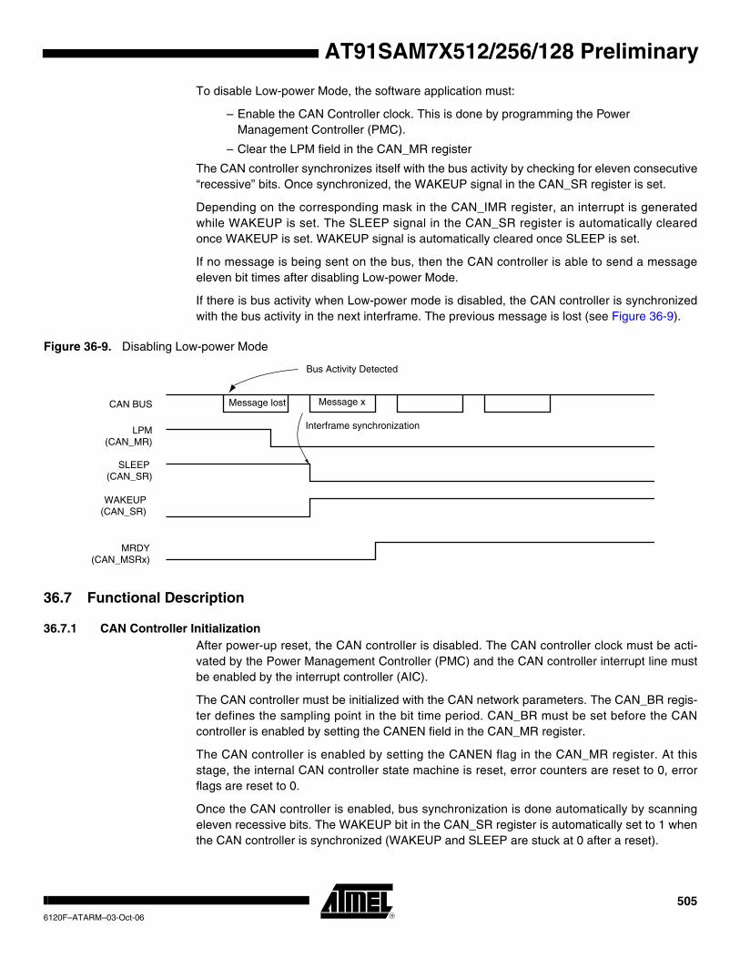
AT91SAM7X512/256/128 Preliminary
To disable Low-power Mode, the software application must:
– Enable the CAN Controller clock. This is done by programming the Power Management Controller (PMC).
– Clear the LPM field in the CAN_MR register
The CAN controller synchronizes itself with the bus activity by checking for eleven consecutive “recessive” bits. Once synchronized, the WAKEUP signal in the CAN_SR register is set.
Depending on the corresponding mask in the CAN_IMR register, an interrupt is generated while WAKEUP is set. The SLEEP signal in the CAN_SR register is automatically cleared once WAKEUP is set. WAKEUP signal is automatically cleared once SLEEP is set.
If no message is being sent on the bus, then the CAN controller is able to send a message eleven bit times after disabling Low-power Mode.
If there is bus activity when Low-power mode is disabled, the CAN controller is synchronized with the bus activity in the next interframe. The previous message is lost (see Figure 36-9).
Figure 36-9. Disabling Low-power Mode
36.7 Functional Description
36.7.1 CAN Controller InitializationAfter power-up reset, the CAN controller is disabled. The CAN controller clock must be acti-vated by the Power Management Controller (PMC) and the CAN controller interrupt line must be enabled by the interrupt controller (AIC).
The CAN controller must be initialized with the CAN network parameters. The CAN_BR regis-ter defines the sampling point in the bit time period. CAN_BR must be set before the CAN controller is enabled by setting the CANEN field in the CAN_MR register.
The CAN controller is enabled by setting the CANEN flag in the CAN_MR register. At this stage, the internal CAN controller state machine is reset, error counters are reset to 0, error flags are reset to 0.
Once the CAN controller is enabled, bus synchronization is done automatically by scanning eleven recessive bits. The WAKEUP bit in the CAN_SR register is automatically set to 1 when the CAN controller is synchronized (WAKEUP and SLEEP are stuck at 0 after a reset).
SLEEP (CAN_SR)
MRDY(CAN_MSRx)
LPM(CAN_MR)
CAN BUS
Bus Activity Detected
Message x
Interframe synchronization
WAKEUP(CAN_SR)
Message lost
5056120F–ATARM–03-Oct-06

AT91SAM7X512/256/128 Preliminary
The CAN controller can start listening to the network in Autobaud Mode. In this case, the error counters are locked and a mailbox may be configured in Receive Mode. By scanning error flags, the CAN_BR register values synchronized with the network. Once no error has been detected, the application disables the Autobaud Mode, clearing the ABM field in the CAN_MR register.
Figure 36-10. Possible Initialization Procedure
36.7.2 CAN Controller Interrupt HandlingThere are two different types of interrupts. One type of interrupt is a message-object related interrupt, the other is a system interrupt that handles errors or system-related interrupt sources.
All interrupt sources can be masked by writing the corresponding field in the CAN_IDR regis-ter. They can be unmasked by writing to the CAN_IER register. After a power-up reset, all interrupt sources are disabled (masked). The current mask status can be checked by reading the CAN_IMR register.
The CAN_SR register gives all interrupt source states.
The following events may initiate one of the two interrupts:
• Message object interrupt
– Data registers in the mailbox object are available to the application. In Receive Mode, a new message was received. In Transmit Mode, a message was transmitted successfully.
– A sent transmission was aborted.
Errors ?
No
Yes
(ABM == 1 and CANEN == 1)
CANEN = 1 (ABM == 0)
ABM = 0 and CANEN = 0
(CAN_SR or CAN_MSRx)
Change CAN_BR value
End of Initialization
Configure a Mailbox in Reception Mode
Enable CAN Controller Interrupt Line
Enable CAN Controller Clock
(AIC)
(PMC)
5066120F–ATARM–03-Oct-06
AT91SAM7X512/256/128 Preliminary
• System interrupts
– Bus-off interrupt: The CAN module enters the bus-off state.
– Error-passive interrupt: The CAN module enters Error Passive Mode.
– Error-active Mode: The CAN module is neither in Error Passive Mode nor in Bus-off mode.
– Warn Limit interrupt: The CAN module is in Error-active Mode, but at least one of its error counter value exceeds 96.
– Wake-up interrupt: This interrupt is generated after a wake-up and a bus synchronization.
– Sleep interrupt: This interrupt is generated after a Low-power Mode enable once all pending messages in transmission have been sent.
– Internal timer counter overflow interrupt: This interrupt is generated when the internal timer rolls over.
– Timestamp interrupt: This interrupt is generated after the reception or the transmission of a start of frame or an end of frame. The value of the internal counter is copied in the CAN_TIMESTP register.
All interrupts are cleared by clearing the interrupt source except for the internal timer counter overflow interrupt and the timestamp interrupt. These interrupts are cleared by reading the CAN_SR register.
5076120F–ATARM–03-Oct-06

AT91SAM7X512/256/128 Preliminary
36.7.3 CAN Controller Message Handling
36.7.3.1 Receive HandlingTwo modes are available to configure a mailbox to receive messages. In Receive Mode, the first message received is stored in the mailbox data register. In Receive with Overwrite Mode, the last message received is stored in the mailbox.
Simple Receive Mailbox
A mailbox is in Receive Mode once the MOT field in the CAN_MMRx register has been config-ured. Message ID and Message Acceptance Mask must be set before the Receive Mode is enabled.
After Receive Mode is enabled, the MRDY flag in the CAN_MSR register is automatically cleared until the first message is received. When the first message has been accepted by the mailbox, the MRDY flag is set. An interrupt is pending for the mailbox while the MRDY flag is set. This interrupt can be masked depending on the mailbox flag in the CAN_IMR global register.
Message data are stored in the mailbox data register until the software application notifies that data processing has ended. This is done by asking for a new transfer command, setting the MTCR flag in the CAN_MCRx register. This automatically clears the MRDY signal.
The MMI flag in the CAN_MSRx register notifies the software that a message has been lost by the mailbox. This flag is set when messages are received while MRDY is set in the CAN_MSRx register. This flag is cleared by reading the CAN_MSRs register. A receive mail-box prevents from overwriting the first message by new ones while MRDY flag is set in the CAN_MSRx register. See Figure 36-11.
Figure 36-11. Receive Mailbox
Note: In the case of ARM architecture, CAN_MSRx, CAN_MDLx, CAN_MDHx can be read using an optimized ldm assembler instruction.
Receive with Overwrite Mailbox
Message 1 Message 2 lost Message 3
Message 3 Message 1
Reading CAN_MSRxReading CAN_MDHx & CAN_MDLx
Writing CAN_MCRx
MMI(CAN_MSRx)
MRDY(CAN_MSRx)
CAN BUS
(CAN_MDLxCAN_MDHx)
MTCR(CAN_MCRx)
Message ID = CAN_MIDx
5086120F–ATARM–03-Oct-06
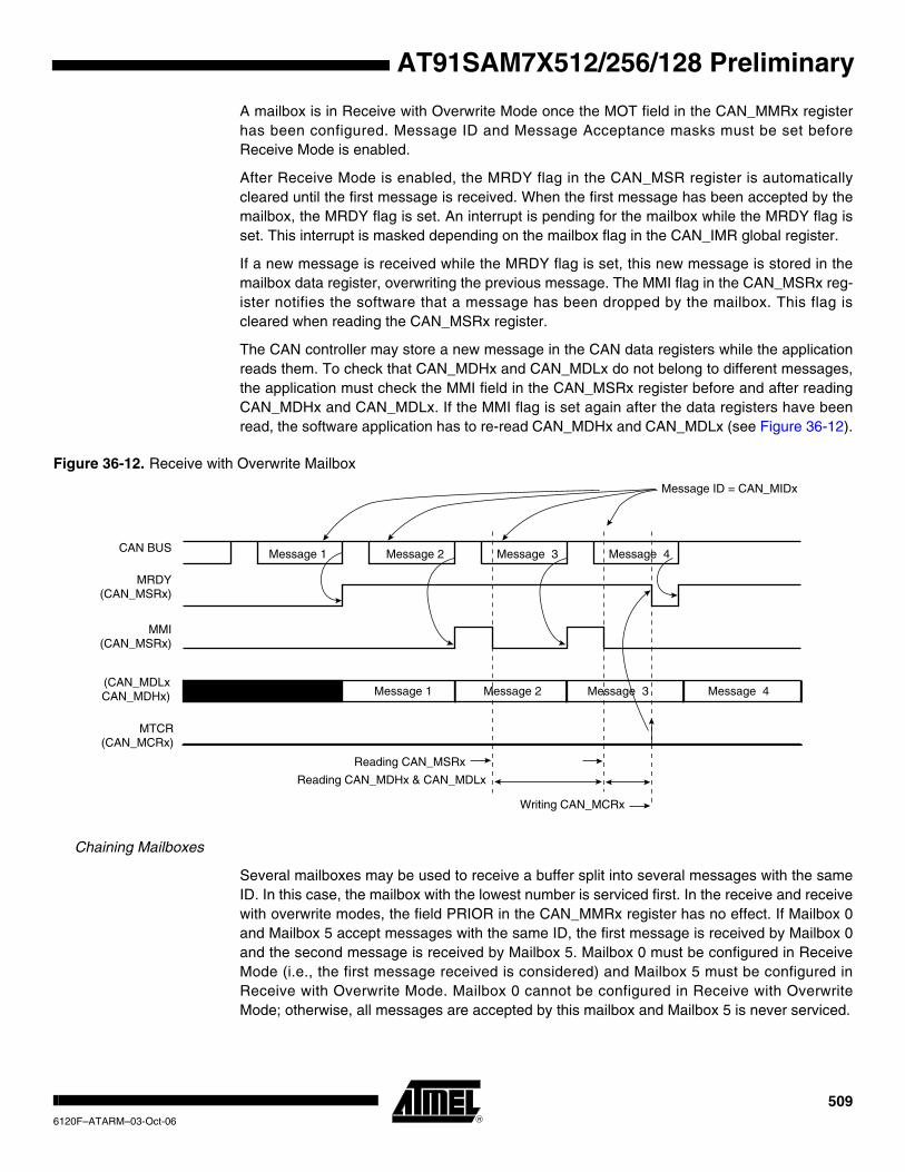
AT91SAM7X512/256/128 Preliminary
A mailbox is in Receive with Overwrite Mode once the MOT field in the CAN_MMRx register has been configured. Message ID and Message Acceptance masks must be set before Receive Mode is enabled.
After Receive Mode is enabled, the MRDY flag in the CAN_MSR register is automatically cleared until the first message is received. When the first message has been accepted by the mailbox, the MRDY flag is set. An interrupt is pending for the mailbox while the MRDY flag is set. This interrupt is masked depending on the mailbox flag in the CAN_IMR global register.
If a new message is received while the MRDY flag is set, this new message is stored in the mailbox data register, overwriting the previous message. The MMI flag in the CAN_MSRx reg-ister notifies the software that a message has been dropped by the mailbox. This flag is cleared when reading the CAN_MSRx register.
The CAN controller may store a new message in the CAN data registers while the application reads them. To check that CAN_MDHx and CAN_MDLx do not belong to different messages, the application must check the MMI field in the CAN_MSRx register before and after reading CAN_MDHx and CAN_MDLx. If the MMI flag is set again after the data registers have been read, the software application has to re-read CAN_MDHx and CAN_MDLx (see Figure 36-12).
Figure 36-12. Receive with Overwrite Mailbox
Chaining Mailboxes
Several mailboxes may be used to receive a buffer split into several messages with the same ID. In this case, the mailbox with the lowest number is serviced first. In the receive and receive with overwrite modes, the field PRIOR in the CAN_MMRx register has no effect. If Mailbox 0 and Mailbox 5 accept messages with the same ID, the first message is received by Mailbox 0 and the second message is received by Mailbox 5. Mailbox 0 must be configured in Receive Mode (i.e., the first message received is considered) and Mailbox 5 must be configured in Receive with Overwrite Mode. Mailbox 0 cannot be configured in Receive with Overwrite Mode; otherwise, all messages are accepted by this mailbox and Mailbox 5 is never serviced.
Message 1 Message 2 Message 3
Message 3 Message 1
Reading CAN_MSRx
Reading CAN_MDHx & CAN_MDLx
Writing CAN_MCRx
MMI(CAN_MSRx)
MRDY(CAN_MSRx)
CAN BUS
(CAN_MDLxCAN_MDHx)
MTCR(CAN_MCRx)
Message ID = CAN_MIDx
Message 4
Message 2 Message 4
5096120F–ATARM–03-Oct-06
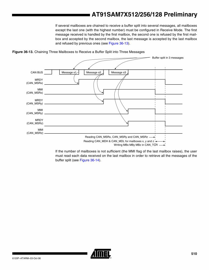
AT91SAM7X512/256/128 Preliminary
If several mailboxes are chained to receive a buffer split into several messages, all mailboxes except the last one (with the highest number) must be configured in Receive Mode. The first message received is handled by the first mailbox, the second one is refused by the first mail-box and accepted by the second mailbox, the last message is accepted by the last mailbox and refused by previous ones (see Figure 36-13).
Figure 36-13. Chaining Three Mailboxes to Receive a Buffer Split into Three Messages
If the number of mailboxes is not sufficient (the MMI flag of the last mailbox raises), the user must read each data received on the last mailbox in order to retrieve all the messages of the buffer split (see Figure 36-14).
MMI(CAN_MSRx)
MRDY(CAN_MSRx)
CAN BUS Message s1
Reading CAN_MSRx, CAN_MSRy and CAN_MSRz
Writing MBx MBy MBz in CAN_TCRReading CAN_MDH & CAN_MDL for mailboxes x, y and z
MMI(CAN_MSRy)
MRDY(CAN_MSRy)
MMI(CAN_MSRz)
MRDY(CAN_MSRz)
Message s2 Message s3
Buffer split in 3 messages
5106120F–ATARM–03-Oct-06

AT91SAM7X512/256/128 Preliminary
Figure 36-14. Chaining Three Mailboxes to Receive a Buffer Split into Four Messages
36.7.3.2 Transmission HandlingA mailbox is in Transmit Mode once the MOT field in the CAN_MMRx register has been con-figured. Message ID and Message Acceptance mask must be set before Receive Mode is enabled.
After Transmit Mode is enabled, the MRDY flag in the CAN_MSR register is automatically set until the first command is sent. When the MRDY flag is set, the software application can pre-pare a message to be sent by writing to the CAN_MDx registers. The message is sent once the software asks for a transfer command setting the MTCR bit and the message data length in the CAN_MCRx register.
The MRDY flag remains at zero as long as the message has not been sent or aborted. It is important to note that no access to the mailbox data register is allowed while the MRDY flag is cleared. An interrupt is pending for the mailbox while the MRDY flag is set. This interrupt can be masked depending on the mailbox flag in the CAN_IMR global register.
It is also possible to send a remote frame setting the MRTR bit instead of setting the MDLC field. The answer to the remote frame is handled by another reception mailbox. In this case, the device acts as a consumer but with the help of two mailboxes. It is possible to handle the remote frame emission and the answer reception using only one mailbox configured in Con-sumer Mode. Refer to the section ”Remote Frame Handling” on page 512.
Several messages can try to win the bus arbitration in the same time. The message with the highest priority is sent first. Several transfer request commands can be generated at the same time by setting MBx bits in the CAN_TCR register. The priority is set in the PRIOR field of the CAN_MMRx register. Priority 0 is the highest priority, priority 15 is the lowest priority. Thus it is possible to use a part of the message ID to set the PRIOR field. If two mailboxes have the same priority, the message of the mailbox with the lowest number is sent first. Thus if mailbox
MMI(CAN_MSRx)
MRDY(CAN_MSRx)
CAN BUS Message s1
Reading CAN_MSRx, CAN_MSRy and CAN_MSRz
Writing MBx MBy MBz in CAN_TCRReading CAN_MDH & CAN_MDL for mailboxes x, y and z
MMI(CAN_MSRy)
MRDY(CAN_MSRy)
MMI(CAN_MSRz)
MRDY(CAN_MSRz)
Message s2 Message s3
Buffer split in 4 messages
Message s4
5116120F–ATARM–03-Oct-06

AT91SAM7X512/256/128 Preliminary
0 and mailbox 5 have the same priority and have a message to send at the same time, then the message of the mailbox 0 is sent first.
Setting the MACR bit in the CAN_MCRx register aborts the transmission. Transmission for several mailboxes can be aborted by writing MBx fields in the CAN_MACR register. If the message is being sent when the abort command is set, then the application is notified by the MRDY bit set and not the MABT in the CAN_MSRx register. Otherwise, if the message has not been sent, then the MRDY and the MABT are set in the CAN_MSR register.
When the bus arbitration is lost by a mailbox message, the CAN controller tries to win the next bus arbitration with the same message if this one still has the highest priority. Messages to be sent are re-tried automatically until they win the bus arbitration. This feature can be disabled by setting the bit DRPT in the CAN_MR register. In this case if the message was not sent the first time it was transmitted to the CAN transceiver, it is automatically aborted. The MABT flag is set in the CAN_MSRx register until the next transfer command.
Figure 36-15 shows three MBx message attempts being made (MRDY of MBx set to 0).
The first MBx message is sent, the second is aborted and the last one is trying to be aborted but too late because it has already been transmitted to the CAN transceiver.
Figure 36-15. Transmitting Messages
36.7.3.3 Remote Frame HandlingProducer/consumer model is an efficient means of handling broadcasted messages. The push model allows a producer to broadcast messages; the pull model allows a customer to ask for messages.
MTCR(CAN_MCRx)
MRDY(CAN_MSRx)
CAN BUS MBx message
Reading CAN_MSRx
Writing CAN_MDHx & CAN_MDLx
MBx message
MACR(CAN_MCRx)
Abort MBx message Try to Abort MBx message
MABT(CAN_MSRx)
5126120F–ATARM–03-Oct-06

AT91SAM7X512/256/128 Preliminary
Figure 36-16. Producer / Consumer Model
In Pull Mode, a consumer transmits a remote frame to the producer. When the producer receives a remote frame, it sends the answer accepted by one or many consumers. Using transmit and receive mailboxes, a consumer must dedicate two mailboxes, one in Transmit Mode to send remote frames, and at least one in Receive Mode to capture the producer’s answer. The same structure is applicable to a producer: one reception mailbox is required to get the remote frame and one transmit mailbox to answer.
Mailboxes can be configured in Producer or Consumer Mode. A lonely mailbox can handle the remote frame and the answer. With 8 mailboxes, the CAN controller can handle 8 independent producers/consumers.
Producer Configuration
A mailbox is in Producer Mode once the MOT field in the CAN_MMRx register has been con-figured. Message ID and Message Acceptance masks must be set before Receive Mode is enabled.
After Producer Mode is enabled, the MRDY flag in the CAN_MSR register is automatically set until the first transfer command. The software application prepares data to be sent by writing to the CAN_MDHx and the CAN_MDLx registers, then by setting the MTCR bit in the CAN_MCRx register. Data is sent after the reception of a remote frame as soon as it wins the bus arbitration.
The MRDY flag remains at zero as long as the message has not been sent or aborted. No access to the mailbox data register can be done while MRDY flag is cleared. An interrupt is pending for the mailbox while the MRDY flag is set. This interrupt can be masked according to the mailbox flag in the CAN_IMR global register.
If a remote frame is received while no data are ready to be sent (signal MRDY set in the CAN_MSRx register), then the MMI signal is set in the CAN_MSRx register. This bit is cleared by reading the CAN_MSRx register.
CAN Data Frame
CAN Remote Frame
CAN Data Frame
Indication(s)Request
Request(s)Indications
Response
Confirmation(s)
PUSH MODEL
PULL MODEL
Producer
Producer
Consumer
Consumer
5136120F–ATARM–03-Oct-06

AT91SAM7X512/256/128 Preliminary
The MRTR field in the CAN_MSRx register has no meaning. This field is used only when using Receive and Receive with Overwrite modes.
After a remote frame has been received, the mailbox functions like a transmit mailbox. The message with the highest priority is sent first. The transmitted message may be aborted by setting the MACR bit in the CAN_MCR register. Please refer to the section ”Transmission Handling” on page 511.
Figure 36-17. Producer Handling
Consumer Configuration
A mailbox is in Consumer Mode once the MOT field in the CAN_MMRx register has been con-figured. Message ID and Message Acceptance masks must be set before Receive Mode is enabled.
After Consumer Mode is enabled, the MRDY flag in the CAN_MSR register is automatically cleared until the first transfer request command. The software application sends a remote frame by setting the MTCR bit in the CAN_MCRx register or the MBx bit in the global CAN_TCR register. The application is notified of the answer by the MRDY flag set in the CAN_MSRx register. The application can read the data contents in the CAN_MDHx and CAN_MDLx registers. An interrupt is pending for the mailbox while the MRDY flag is set. This interrupt can be masked according to the mailbox flag in the CAN_IMR global register.
The MRTR bit in the CAN_MCRx register has no effect. This field is used only when using Transmit Mode.
After a remote frame has been sent, the consumer mailbox functions as a reception mailbox. The first message received is stored in the mailbox data registers. If other messages intended for this mailbox have been sent while the MRDY flag is set in the CAN_MSRx register, they will be lost. The application is notified by reading the MMI field in the CAN_MSRx register. The read operation automatically clears the MMI flag.
If several messages are answered by the Producer, the CAN controller may have one mailbox in consumer configuration, zero or several mailboxes in Receive Mode and one mailbox in Receive with Overwrite Mode. In this case, the consumer mailbox must have a lower number than the Receive with Overwrite mailbox. The transfer command can be triggered for all mail-boxes at the same time by setting several MBx fields in the CAN_TCR register.
MTCR(CAN_MCRx)
MRDY(CAN_MSRx)
CAN BUS Remote Frame Message 1
Message 1
Message 2
(CAN_MDLxCAN_MDHx)
MMI(CAN_MSRx)
Remote Frame Remote Frame
Message 2
Reading CAN_MSRx
5146120F–ATARM–03-Oct-06
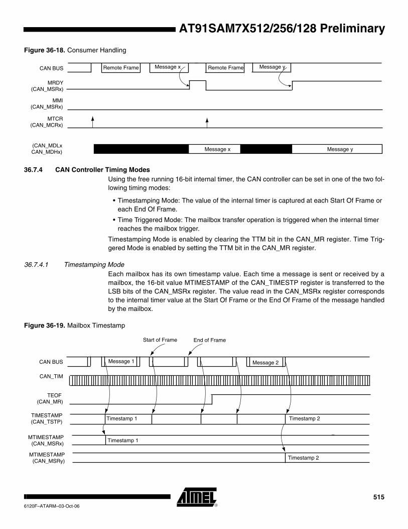
AT91SAM7X512/256/128 Preliminary
Figure 36-18. Consumer Handling
36.7.4 CAN Controller Timing ModesUsing the free running 16-bit internal timer, the CAN controller can be set in one of the two fol-lowing timing modes:
• Timestamping Mode: The value of the internal timer is captured at each Start Of Frame or each End Of Frame.
• Time Triggered Mode: The mailbox transfer operation is triggered when the internal timer reaches the mailbox trigger.
Timestamping Mode is enabled by clearing the TTM bit in the CAN_MR register. Time Trig-gered Mode is enabled by setting the TTM bit in the CAN_MR register.
36.7.4.1 Timestamping ModeEach mailbox has its own timestamp value. Each time a message is sent or received by a mailbox, the 16-bit value MTIMESTAMP of the CAN_TIMESTP register is transferred to the LSB bits of the CAN_MSRx register. The value read in the CAN_MSRx register corresponds to the internal timer value at the Start Of Frame or the End Of Frame of the message handled by the mailbox.
Figure 36-19. Mailbox Timestamp
MTCR(CAN_MCRx)
MRDY(CAN_MSRx)
CAN BUS Remote Frame Message x
Message y
Message y
(CAN_MDLxCAN_MDHx)
MMI(CAN_MSRx)
Remote Frame
Message x
TEOF (CAN_MR)
MTIMESTAMP(CAN_MSRx)
CAN_TIM
CAN BUS
MTIMESTAMP(CAN_MSRy)
Message 1 Message 2
Start of Frame
TIMESTAMP(CAN_TSTP)
End of Frame
Timestamp 1
Timestamp 1
Timestamp 2
Timestamp 2
5156120F–ATARM–03-Oct-06
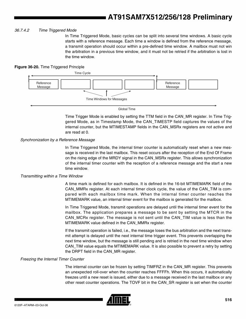
AT91SAM7X512/256/128 Preliminary
36.7.4.2 Time Triggered ModeIn Time Triggered Mode, basic cycles can be split into several time windows. A basic cycle starts with a reference message. Each time a window is defined from the reference message, a transmit operation should occur within a pre-defined time window. A mailbox must not win the arbitration in a previous time window, and it must not be retried if the arbitration is lost in the time window.
Figure 36-20. Time Triggered Principle
Time Trigger Mode is enabled by setting the TTM field in the CAN_MR register. In Time Trig-gered Mode, as in Timestamp Mode, the CAN_TIMESTP field captures the values of the internal counter, but the MTIMESTAMP fields in the CAN_MSRx registers are not active and are read at 0.
Synchronization by a Reference Message
In Time Triggered Mode, the internal timer counter is automatically reset when a new mes-sage is received in the last mailbox. This reset occurs after the reception of the End Of Frame on the rising edge of the MRDY signal in the CAN_MSRx register. This allows synchronization of the internal timer counter with the reception of a reference message and the start a new time window.
Transmitting within a Time Window
A time mark is defined for each mailbox. It is defined in the 16-bit MTIMEMARK field of the CAN_MMRx register. At each internal timer clock cycle, the value of the CAN_TIM is com-pared with each mailbox time mark. When the internal timer counter reaches the MTIMEMARK value, an internal timer event for the mailbox is generated for the mailbox.
In Time Triggered Mode, transmit operations are delayed until the internal timer event for the mailbox. The application prepares a message to be sent by setting the MTCR in the CAN_MCRx register. The message is not sent until the CAN_TIM value is less than the MTIMEMARK value defined in the CAN_MMRx register.
If the transmit operation is failed, i.e., the message loses the bus arbitration and the next trans-mit attempt is delayed until the next internal time trigger event. This prevents overlapping the next time window, but the message is still pending and is retried in the next time window when CAN_TIM value equals the MTIMEMARK value. It is also possible to prevent a retry by setting the DRPT field in the CAN_MR register.
Freezing the Internal Timer Counter
The internal counter can be frozen by setting TIMFRZ in the CAN_MR register. This prevents an unexpected roll-over when the counter reaches FFFFh. When this occurs, it automatically freezes until a new reset is issued, either due to a message received in the last mailbox or any other reset counter operations. The TOVF bit in the CAN_SR register is set when the counter
ReferenceMessage
ReferenceMessage
Global Time
Time Cycle
Time Windows for Messages
5166120F–ATARM–03-Oct-06

AT91SAM7X512/256/128 Preliminary
is frozen. The TOVF bit in the CAN_SR register is cleared by reading the CAN_SR register. Depending on the corresponding interrupt mask in the CAN_IMR register, an interrupt is gen-erated when TOVF is set.
Figure 36-21. Time Triggered Operations
MRDY(CAN_MSRlast_mailbox_number)
CAN_TIM
CAN BUS
MRDY(CAN_MSRx)
End of Frame
Timer Event x MTIMEMARKx == CAN_TIM
Timer Event y
MRDY(CAN_MSRy)
MTIMEMARKy == CAN_TIM
Cleared by software
Internal Counter Reset
Message xArbitration Lost
Message yArbitration Win
Reference Message Message y
MRDY(CAN_MSRlast_mailbox_number)
CAN_TIM
CAN BUS
MRDY(CAN_MSRx)
End of Frame
Timer Event x MTIMEMARKx == CAN_TIM
Cleared by software
Internal Counter Reset
Message xArbitration Win
Reference Message Message x
Basic Cycle
Time Window
Basic Cycle
Time Window
5176120F–ATARM–03-Oct-06

AT91SAM7X512/256/128 Preliminary
36.8 Controller Area Network (CAN) User Interface
Table 36-4. CAN Memory Map
Offset Register Name Access Reset State
0x0000 Mode Register CAN_MR Read-Write 0x0
0x0004 Interrupt Enable Register CAN_IER Write-only -
0x0008 Interrupt Disable Register CAN_IDR Write-only -
0x000C Interrupt Mask Register CAN_IMR Read-only 0x0
0x0010 Status Register CAN_SR Read-only 0x0
0x0014 Baudrate Register CAN_BR Read/Write 0x0
0x0018 Timer Register CAN_TIM Read-only 0x0
0x001C Timestamp Register CAN_TIMESTP Read-only 0x0
0x0020 Error Counter Register CAN_ECR Read-only 0x0
0x0024 Transfer Command Register CAN_TCR Write-only -
0x0028 Abort Command Register CAN_ACR Write-only -
0x0100 - 0x01FC Reserved – – –
0x0200 Mailbox 0 Mode Register CAN_MMR0 Read/Write 0x0
0x0204 Mailbox 0 Acceptance Mask Register CAN_MAM0 Read/Write 0x0
0x0208 Mailbox 0 ID Register CAN_MID0 Read/Write 0x0
0x020C Mailbox 0 Family ID Register CAN_MFID0 Read-only 0x0
0x0210 Mailbox 0 Status Register CAN_MSR0 Read-only 0x0
0x0214 Mailbox 0 Data Low Register CAN_MDL0 Read/Write 0x0
0x0218 Mailbox 0 Data High Register CAN_MDH0 Read/Write 0x0
0x021C Mailbox 0 Control Register CAN_MCR0 Write-only -
0x0220 Mailbox 1 Mode Register CAN_MMR1 Read/Write 0x0
0x0224 Mailbox 1 Acceptance Mask Register CAN_MAM1 Read/Write 0x0
0x0228 Mailbox 1 ID register CAN_MID1 Read/Write 0x0
0x022C Mailbox 1 Family ID Register CAN_MFID1 Read-only 0x0
0x0230 Mailbox 1 Status Register CAN_MSR1 Read-only 0x0
0x0234 Mailbox 1 Data Low Register CAN_MDL1 Read/Write 0x0
0x0238 Mailbox 1 Data High Register CAN_MDH1 Read/Write 0x0
0x023C Mailbox 1 Control Register CAN_MCR1 Write-only -
... ... ... ... -
5186120F–ATARM–03-Oct-06

AT91SAM7X512/256/128 Preliminary
36.8.1 CAN Mode Register
Name: CAN_MR
Access Type: Read/Write
• CANEN: CAN Controller Enable
0 = The CAN Controller is disabled.
1 = The CAN Controller is enabled.
• LPM: Disable/Enable Low Power Mode
0 = Disable w Power Mode.
1 = Enable Low Power Mo
CAN controller enters Low Power Mode once all pending messages have been transmitted.
• ABM: Disable/Enable Autobaud/Listen mode
0 = Disable Autobaud/listen mode.
1 = Enable Autobaud/listen mode.
• OVL: Disable/Enable Overload Frame
0 = No overload frame is generated.
1 = An overload frame is generated after each successful reception for mailboxes configured in Receive with/without over-write Mode, Producer and Consumer.
• TEOF: Timestamp messages at each end of Frame
0 = The value of CAN_TIM is captured in the CAN_TIMESTP register at each Start Of Frame.
1 = The value of CAN_TIM is captured in the CAN_TIMESTP register at each End Of Frame.
• TTM: Disable/Enable Time Triggered Mode
0 = Time Triggered Mode is disabled.
1 = Time Triggered Mode is enabled.
• TIMFRZ: Enable Timer Freeze
0 = The internal timer continues to be incremented after it reached 0xFFFF.
1 = The internal timer stops incrementing after reaching 0xFFFF. It is restarted after a timer reset. See ”Freezing the Inter-nal Timer Counter” on page 516.
• DRPT: Disable Repeat
0 = When a transmit mailbox loses the bus arbitration, the transfer request remains pending.
1 = When a transmit mailbox lose the bus arbitration, the transfer request is automatically aborted. It automatically raises the MABT and MRDT flags in the corresponding CAN_MSRx.
31 30 29 28 27 26 25 24– – – – –
23 22 21 20 19 18 17 16
– – – – – – – –
15 14 13 12 11 10 9 8
– – – – – – – –
7 6 5 4 3 2 1 0
DRPT TIMFRZ TTM TEOF OVL ABM LPM CANEN
5196120F–ATARM–03-Oct-06
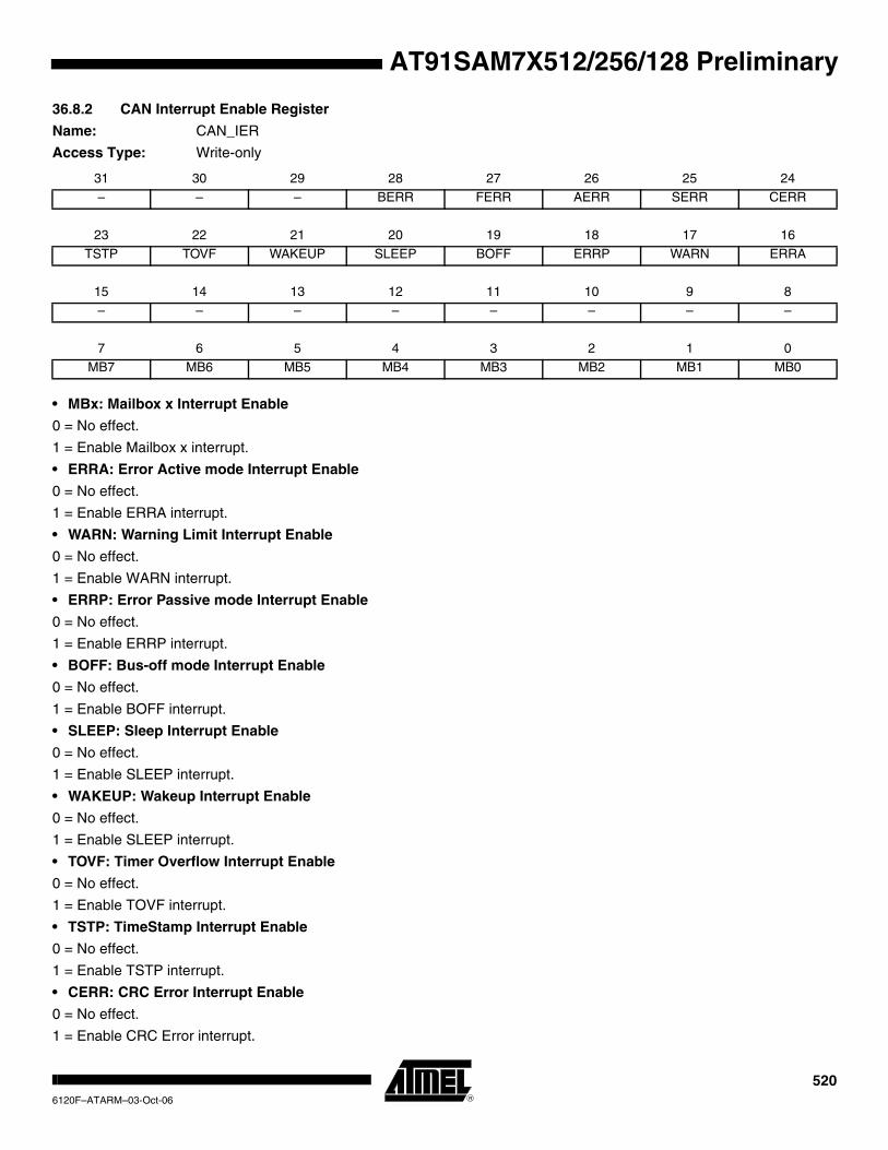
AT91SAM7X512/256/128 Preliminary
36.8.2 CAN Interrupt Enable Register
Name: CAN_IER
Access Type: Write-only
• MBx: Mailbox x Interrupt Enable
0 = No effect.
1 = Enable Mailbox x interrupt.
• ERRA: Error Active mode Interrupt Enable
0 = No effect.
1 = Enable ERRA interrupt.
• WARN: Warning Limit Interrupt Enable
0 = No effect.
1 = Enable WARN interrupt.
• ERRP: Error Passive mode Interrupt Enable
0 = No effect.
1 = Enable ERRP interrupt.
• BOFF: Bus-off mode Interrupt Enable
0 = No effect.
1 = Enable BOFF interrupt.
• SLEEP: Sleep Interrupt Enable
0 = No effect.
1 = Enable SLEEP interrupt.
• WAKEUP: Wakeup Interrupt Enable
0 = No effect.
1 = Enable SLEEP interrupt.
• TOVF: Timer Overflow Interrupt Enable
0 = No effect.
1 = Enable TOVF interrupt.
• TSTP: TimeStamp Interrupt Enable
0 = No effect.
1 = Enable TSTP interrupt.
• CERR: CRC Error Interrupt Enable
0 = No effect.
1 = Enable CRC Error interrupt.
31 30 29 28 27 26 25 24– – – BERR FERR AERR SERR CERR
23 22 21 20 19 18 17 16
TSTP TOVF WAKEUP SLEEP BOFF ERRP WARN ERRA
15 14 13 12 11 10 9 8
– – – – – – – –
7 6 5 4 3 2 1 0
MB7 MB6 MB5 MB4 MB3 MB2 MB1 MB0
5206120F–ATARM–03-Oct-06

AT91SAM7X512/256/128 Preliminary
• SERR: Stuffing Error Interrupt Enable
0 = No effect.
1 = Enable Stuffing Error interrupt.
• AERR: Acknowledgment Error Interrupt Enable
0 = No effect.
1 = Enable Acknowledgment Error interrupt.
• FERR: Form Error Interrupt Enable
0 = No effect.
1 = Enable Form Error interrupt.
• BERR: Bit Error Interrupt Enable
0 = No effect.
1 = Enable Bit Error interrupt.
5216120F–ATARM–03-Oct-06

AT91SAM7X512/256/128 Preliminary
36.8.3 CAN Interrupt Disable Register
Name: CAN_IDR
Access Type: Write-only
• MBx: Mailbox x Interrupt Disable
0 = No effect.
1 = Disable Mailbox x interrupt.
• ERRA: Error Active Mode Interrupt Disable
0 = No effect.
1 = Disable ERRA interrupt.
• WARN: Warning Limit Interrupt Disable
0 = No effect.
1 = Disable WARN interrupt.
• ERRP: Error Passive mode Interrupt Disable
0 = No effect.
1 = Disable ERRP interrupt.
• BOFF: Bus-off mode Interrupt Disable
0 = No effect.
1 = Disable BOFF interrupt.
• SLEEP: Sleep Interrupt Disable
0 = No effect.
1 = Disable SLEEP interrupt.
• WAKEUP: Wakeup Interrupt Disable
0 = No effect.
1 = Disable WAKEUP interrupt.
• TOVF: Timer Overflow Interrupt
0 = No effect.
1 = Disable TOVF interrupt.
• TSTP: TimeStamp Interrupt Disable
0 = No effect.
1 = Disable TSTP interrupt.
• CERR: CRC Error Interrupt Disable
0 = No effect.
1 = Disable CRC Error interrupt.
31 30 29 28 27 26 25 24– – – BERR FERR AERR SERR CERR
23 22 21 20 19 18 17 16
TSTP TOVF WAKEUP SLEEP BOFF ERRP WARN ERRA
15 14 13 12 11 10 9 8
– – – – – – – –
7 6 5 4 3 2 1 0
MB7 MB6 MB5 MB4 MB3 MB2 MB1 MB0
5226120F–ATARM–03-Oct-06

AT91SAM7X512/256/128 Preliminary
• SERR: Stuffing Error Interrupt Disable
0 = No effect.
1 = Disable Stuffing Error interrupt.
• AERR: Acknowledgment Error Interrupt Disable
0 = No effect.
1 = Disable Acknowledgment Error interrupt.
• FERR: Form Error Interrupt Disable
0 = No effect.
1 = Disable Form Error interrupt.
• BERR: Bit Error Interrupt Disable
0 = No effect.
1 = Disable Bit Error interrupt.
5236120F–ATARM–03-Oct-06

AT91SAM7X512/256/128 Preliminary
36.8.4 CAN Interrupt Mask Register
Name: CAN_IMR
Access Type: Read-only
• MBx: Mailbox x Interrupt Mask
0 = Mailbox x interrupt is disabled.
1 = Mailbox x interrupt is enabled.
• ERRA: Error Active mode Interrupt Mask
0 = ERRA interrupt is disabled.
1 = ERRA interrupt is enabled.
• WARN: Warning Limit Interrupt Mask
0 = Warning Limit interrupt is disabled.
1 = Warning Limit interrupt is enabled.
• ERRP: Error Passive Mode Interrupt Mask
0 = ERRP interrupt is disabled.
1 = ERRP interrupt is enabled.
• BOFF: Bus-off Mode Interrupt Mask
0 = BOFF interrupt is disabled.
1 = BOFF interrupt is enabled.
• SLEEP: Sleep Interrupt Mask
0 = SLEEP interrupt is disabled.
1 = SLEEP interrupt is enabled.
• WAKEUP: Wakeup Interrupt Mask
0 = WAKEUP interrupt is disabled.
1 = WAKEUP interrupt is enabled.
• TOVF: Timer Overflow Interrupt Mask
0 = TOVF interrupt is disabled.
1 = TOVF interrupt is enabled.
• TSTP: Timestamp Interrupt Mask
0 = TSTP interrupt is disabled.
1 = TSTP interrupt is enabled.
• CERR: CRC Error Interrupt Mask
0 = CRC Error interrupt is disabled.
1 = CRC Error interrupt is enabled.
31 30 29 28 27 26 25 24– – – BERR FERR AERR SERR CERR
23 22 21 20 19 18 17 16
TSTP TOVF WAKEUP SLEEP BOFF ERRP WARN ERRA
15 14 13 12 11 10 9 8
– – – – – – – –
7 6 5 4 3 2 1 0
MB7 MB6 MB5 MB4 MB3 MB2 MB1 MB0
5246120F–ATARM–03-Oct-06

AT91SAM7X512/256/128 Preliminary
• SERR: Stuffing Error Interrupt Mask
0 = Bit Stuffing Error interrupt is disabled.
1 = Bit Stuffing Error interrupt is enabled.
• AERR: Acknowledgment Error Interrupt Mask
0 = Acknowledgment Error interrupt is disabled.
1 = Acknowledgment Error interrupt is enabled.
• FERR: Form Error Interrupt Mask
0 = Form Error interrupt is disabled.
1 = Form Error interrupt is enabled.
• BERR: Bit Error Interrupt Mask
0 = Bit Error interrupt is disabled.
1 = Bit Error interrupt is enabled.
5256120F–ATARM–03-Oct-06
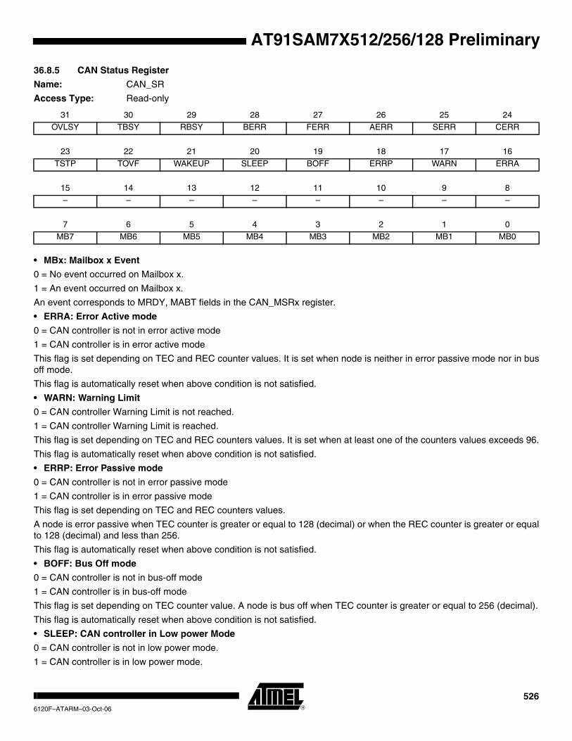
AT91SAM7X512/256/128 Preliminary
36.8.5 CAN Status Register
Name: CAN_SR
Access Type: Read-only
• MBx: Mailbox x Event
0 = No event occurred on Mailbox x.
1 = An event occurred on Mailbox x.
An event corresponds to MRDY, MABT fields in the CAN_MSRx register.
• ERRA: Error Active mode
0 = CAN controller is not in error active mode
1 = CAN controller is in error active mode
This flag is set depending on TEC and REC counter values. It is set when node is neither in error passive mode nor in bus off mode.
This flag is automatically reset when above condition is not satisfied.
• WARN: Warning Limit
0 = CAN controller Warning Limit is not reached.
1 = CAN controller Warning Limit is reached.
This flag is set depending on TEC and REC counters values. It is set when at least one of the counters values exceeds 96.
This flag is automatically reset when above condition is not satisfied.
• ERRP: Error Passive mode
0 = CAN controller is not in error passive mode
1 = CAN controller is in error passive mode
This flag is set depending on TEC and REC counters values.
A node is error passive when TEC counter is greater or equal to 128 (decimal) or when the REC counter is greater or equal to 128 (decimal) and less than 256.
This flag is automatically reset when above condition is not satisfied.
• BOFF: Bus Off mode
0 = CAN controller is not in bus-off mode
1 = CAN controller is in bus-off mode
This flag is set depending on TEC counter value. A node is bus off when TEC counter is greater or equal to 256 (decimal).
This flag is automatically reset when above condition is not satisfied.
• SLEEP: CAN controller in Low power Mode
0 = CAN controller is not in low power mode.
1 = CAN controller is in low power mode.
31 30 29 28 27 26 25 24OVLSY TBSY RBSY BERR FERR AERR SERR CERR
23 22 21 20 19 18 17 16
TSTP TOVF WAKEUP SLEEP BOFF ERRP WARN ERRA
15 14 13 12 11 10 9 8
– – – – – – – –
7 6 5 4 3 2 1 0
MB7 MB6 MB5 MB4 MB3 MB2 MB1 MB0
5266120F–ATARM–03-Oct-06

AT91SAM7X512/256/128 Preliminary
This flag is automatically reset when Low power mode is disabled
• WAKEUP: CAN controller is not in Low power Mode
0 = CAN controller is in low power mode.
1 = CAN controller is not in low power mode.
When a WAKEUP event occurs, the CAN controller is synchronized with the bus activity. Messages can be transmitted or received. The CAN controller clock must be available when a WAKEUP event occurs. This flag is automatically reset when the CAN Controller enters Low Power mode.
• TOVF: Timer Overflow
0 = The timer has not rolled-over FFFFh to 0000h.
1 = The timer rolls-over FFFFh to 0000h.
This flag is automatically cleared by reading CAN_SR register.
• TSTP Timestamp
0 = No bus activity has been detected.
1 = A start of frame or an end of frame has been detected (according to the TEOF field in the CAN_MR register).
This flag is automatically cleared by reading the CAN_SR register.
• CERR: Mailbox CRC Error
0 = No CRC error occurred during a previous transfer.
1 = A CRC error occurred during a previous transfer.
A CRC error has been detected during last reception.
This flag is automatically cleared by reading CAN_SR register.
• SERR: Mailbox Stuffing Error
0 = No stuffing error occurred during a previous transfer.
1 = A stuffing error occurred during a previous transfer.
A form error results from the detection of more than five consecutive bit with the same polarity.
This flag is automatically cleared by reading CAN_SR register.
• AERR: Acknowledgment Error
0 = No acknowledgment error occurred during a previous transfer.
1 = An acknowledgment error occurred during a previous transfer.
An acknowledgment error is detected when no detection of the dominant bit in the acknowledge slot occurs.
This flag is automatically cleared by reading CAN_SR register.
• FERR: Form Error
0 = No form error occurred during a previous transfer
1 = A form error occurred during a previous transfer
A form error results from violations on one or more of the fixed form of the following bit fields:
– CRC delimiter
– ACK delimiter
– End of frame
– Error delimiter
– Overload delimiter
This flag is automatically cleared by reading CAN_SR register.
• BERR: Bit Error
0 = No bit error occurred during a previous transfer.
1 = A bit error occurred during a previous transfer.
5276120F–ATARM–03-Oct-06
AT91SAM7X512/256/128 Preliminary
A bit error is set when the bit value monitored on the line is different from the bit value sent.
This flag is automatically cleared by reading CAN_SR register.
• RBSY: Receiver busy
0 = CAN receiver is not receiving a frame.
1 = CAN receiver is receiving a frame.
Receiver busy. This status bit is set by hardware while CAN receiver is acquiring or monitoring a frame (remote, data, over-load or error frame). It is automatically reset when CAN is not receiving.
• TBSY: Transmitter busy
0 = CAN transmitter is not transmitting a frame.
1 = CAN transmitter is transmitting a frame.
Transmitter busy. This status bit is set by hardware while CAN transmitter is generating a frame (remote, data, overload or error frame). It is automatically reset when CAN is not transmitting.
• OVLSY: Overload busy
0 = CAN transmitter is not transmitting an overload frame.
1 = CAN transmitter is transmitting a overload frame.
It is automatically reset when the bus is not transmitting an overload frame.
5286120F–ATARM–03-Oct-06

AT91SAM7X512/256/128 Preliminary
36.8.6 CAN Baudrate Register
Name: CAN_BR
Access Type: Read/Write
Any modification on one of the fields of the CANBR register must be done while CAN module is disabled.
To compute the different Bit Timings, please refer to the Section 36.6.4.1 ”CAN Bit Timing Configuration” on page 498.
• PHASE2: Phase 2 segment
This phase is used to compensate the edge phase error.
Warning: PHASE2 value must be different from 0.
• PHASE1: Phase 1 segment
This phase is used to compensate for edge phase error.
• PROPAG: Programming time segment
This part of the bit time is used to compensate for the physical delay times within the network.
• SJW: Re-synchronization jump width
To compensate for phase shifts between clock oscillators of different controllers on bus. The controller must re-synchronize on any relevant signal edge of the current transmission. The synchronization jump width defines the maximum of clock cycles a bit period may be shortened or lengthened by re-synchronization.
• BRP: Baudrate Prescaler.
This field allows user to program the period of the CAN system clock to determine the individual bit timing.
The BRP field must be within the range [1, 0x7F], i.e., BRP = 0 is not authorized.
• SMP: Sampling Mode
0 = The incoming bit stream is sampled once at sample point.
1 = The incoming bit stream is sampled three times with a period of a MCK clock period, centered on sample point.
SMP Sampling Mode is automatically disabled if BRP = 0.
31 30 29 28 27 26 25 24– – – – – – – SMP
23 22 21 20 19 18 17 16
– BRP
15 14 13 12 11 10 9 8
– – SJW – PROPAG
7 6 5 4 3 2 1 0
– PHASE1 – PHASE2
tPHS2 tCSC PHASE2 1+( )×=
tPHS1 tCSC PHASE1 1+( )×=
tPRS tCSC PROPAG 1+( )×=
tSJW tCSC SJW 1+( )×=
tCSC BRP 1+( ) MCK⁄=
5296120F–ATARM–03-Oct-06

AT91SAM7X512/256/128 Preliminary
36.8.7 CAN Timer Register
Name: CAN_TIM
Access Type: Read-only
• TIMERx: Timer
This field represents the internal CAN controller 16-bit timer value.
31 30 29 28 27 26 25 24– – – – – – – –
23 22 21 20 19 18 17 16
– – – – – – – –
15 14 13 12 11 10 9 8
TIMER15 TIMER14 TIMER13 TIMER12 TIMER11 TIMER10 TIMER9 TIMER8
7 6 5 4 3 2 1 0
TIMER7 TIMER6 TIMER5 TIMER4 TIMER3 TIMER2 TIMER1 TIMER0
5306120F–ATARM–03-Oct-06
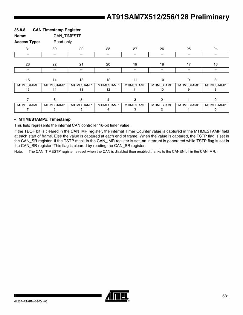
AT91SAM7X512/256/128 Preliminary
36.8.8 CAN Timestamp Register
Name: CAN_TIMESTP
Access Type: Read-only
• MTIMESTAMPx: Timestamp
This field represents the internal CAN controller 16-bit timer value.
If the TEOF bit is cleared in the CAN_MR register, the internal Timer Counter value is captured in the MTIMESTAMP field at each start of frame. Else the value is captured at each end of frame. When the value is captured, the TSTP flag is set in the CAN_SR register. If the TSTP mask in the CAN_IMR register is set, an interrupt is generated while TSTP flag is set in the CAN_SR register. This flag is cleared by reading the CAN_SR register.Note: The CAN_TIMESTP register is reset when the CAN is disabled then enabled thanks to the CANEN bit in the CAN_MR.
31 30 29 28 27 26 25 24– – – – – – – –
23 22 21 20 19 18 17 16
– – – – – – – –
15 14 13 12 11 10 9 8
MTIMESTAMP15
MTIMESTAMP14
MTIMESTAMP13
MTIMESTAMP12
MTIMESTAMP11
MTIMESTAMP10
MTIMESTAMP9
MTIMESTAMP8
7 6 5 4 3 2 1 0
MTIMESTAMP7
MTIMESTAMP6
MTIMESTAMP5
MTIMESTAMP4
MTIMESTAMP3
MTIMESTAMP2
MTIMESTAMP1
MTIMESTAMP0
5316120F–ATARM–03-Oct-06

AT91SAM7X512/256/128 Preliminary
36.8.9 CAN Error Counter Register
Name: CAN_ECR
Access Type: Read-only
• REC: Receive Error Counter
When a receiver detects an error, REC will be increased by one, except when the detected error is a BIT ERROR while sending an ACTIVE ERROR FLAG or an OVERLOAD FLAG.
When a receiver detects a dominant bit as the first bit after sending an ERROR FLAG, REC is increased by 8.
When a receiver detects a BIT ERROR while sending an ACTIVE ERROR FLAG, REC is increased by 8.
Any node tolerates up to 7 consecutive dominant bits after sending an ACTIVE ERROR FLAG, PASSIVE ERROR FLAG or OVERLOAD FLAG. After detecting the 14th consecutive dominant bit (in case of an ACTIVE ERROR FLAG or an OVER-LOAD FLAG) or after detecting the 8th consecutive dominant bit following a PASSIVE ERROR FLAG, and after each sequence of additional eight consecutive dominant bits, each receiver increases its REC by 8.
After successful reception of a message, REC is decreased by 1 if it was between 1 and 127. If REC was 0, it stays 0, and if it was greater than 127, then it is set to a value between 119 and 127.
• TEC: Transmit Error Counter
When a transmitter sends an ERROR FLAG, TEC is increased by 8 except when
– the transmitter is error passive and detects an ACKNOWLEDGMENT ERROR because of not detecting a dominant ACK and does not detect a dominant bit while sending its PASSIVE ERROR FLAG.
– the transmitter sends an ERROR FLAG because a STUFF ERROR occurred during arbitration and should have been recessive and has been sent as recessive but monitored as dominant.
When a transmitter detects a BIT ERROR while sending an ACTIVE ERROR FLAG or an OVERLOAD FLAG, the TEC will be increased by 8.
Any node tolerates up to 7 consecutive dominant bits after sending an ACTIVE ERROR FLAG, PASSIVE ERROR FLAG or OVERLOAD FLAG. After detecting the 14th consecutive dominant bit (in case of an ACTIVE ERROR FLAG or an OVER-LOAD FLAG) or after detecting the 8th consecutive dominant bit following a PASSIVE ERROR FLAG, and after each sequence of additional eight consecutive dominant bits every transmitter increases its TEC by 8.
After a successful transmission the TEC is decreased by 1 unless it was already 0.
31 30 29 28 27 26 25 24– – – – – – – –
23 22 21 20 19 18 17 16
TEC
15 14 13 12 11 10 9 8
– – – – – – – –
7 6 5 4 3 2 1 0
REC
5326120F–ATARM–03-Oct-06
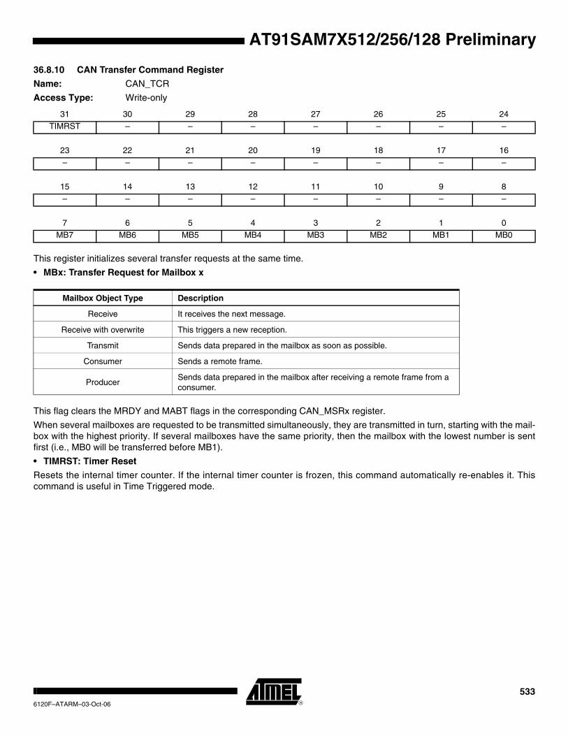
AT91SAM7X512/256/128 Preliminary
36.8.10 CAN Transfer Command Register
Name: CAN_TCR
Access Type: Write-only
This register initializes several transfer requests at the same time.
• MBx: Transfer Request for Mailbox x
This flag clears the MRDY and MABT flags in the corresponding CAN_MSRx register.
When several mailboxes are requested to be transmitted simultaneously, they are transmitted in turn, starting with the mail-box with the highest priority. If several mailboxes have the same priority, then the mailbox with the lowest number is sent first (i.e., MB0 will be transferred before MB1).
• TIMRST: Timer Reset
Resets the internal timer counter. If the internal timer counter is frozen, this command automatically re-enables it. This command is useful in Time Triggered mode.
31 30 29 28 27 26 25 24TIMRST – – – – – – –
23 22 21 20 19 18 17 16
– – – – – – – –
15 14 13 12 11 10 9 8
– – – – – – – –
7 6 5 4 3 2 1 0
MB7 MB6 MB5 MB4 MB3 MB2 MB1 MB0
Mailbox Object Type Description
Receive It receives the next message.
Receive with overwrite This triggers a new reception.
Transmit Sends data prepared in the mailbox as soon as possible.
Consumer Sends a remote frame.
ProducerSends data prepared in the mailbox after receiving a remote frame from a consumer.
5336120F–ATARM–03-Oct-06

AT91SAM7X512/256/128 Preliminary
36.8.11 CAN Abort Command Register
Name: CAN_ACR
Access Type: Write-only
This register initializes several abort requests at the same time.
• MBx: Abort Request for Mailbox x
It is possible to set MACR field (in the CAN_MCRx register) for each mailbox.
31 30 29 28 27 26 25 24– – – – – – – –
23 22 21 20 19 18 17 16
– – – – – – – –
15 14 13 12 11 10 9 8
– – – – – – – –
7 6 5 4 3 2 1 0
MB7 MB6 MB5 MB4 MB3 MB2 MB1 MB0
Mailbox Object Type Description
Receive No action
Receive with overwrite No action
TransmitCancels transfer request if the message has not been transmitted to the CAN transceiver.
Consumer Cancels the current transfer before the remote frame has been sent.
Producer Cancels the current transfer. The next remote frame is not serviced.
5346120F–ATARM–03-Oct-06

AT91SAM7X512/256/128 Preliminary
36.8.12 CAN Message Mode Register
Name: CAN_MMRx
Access Type: Read/Write
• MTIMEMARK: Mailbox Timemark
This field is active in Time Triggered Mode. Transmit operations are allowed when the internal timer counter reaches the Mailbox Timemark. See ”Transmitting within a Time Window” on page 516.
In Timestamp Mode, MTIMEMARK is set to 0.
• PRIOR: Mailbox Priority
This field has no effect in receive and receive with overwrite modes. In these modes, the mailbox with the lowest number is serviced first.
When several mailboxes try to transmit a message at the same time, the mailbox with the highest priority is serviced first. If several mailboxes have the same priority, the mailbox with the lowest number is serviced first (i.e., MBx0 is serviced before MBx 15 if they have the same priority).
• MOT: Mailbox Object Type
This field allows the user to define the type of the mailbox. All mailboxes are independently configurable. Five different types are possible for each mailbox:
31 30 29 28 27 26 25 24– – – – – MOT
23 22 21 20 19 18 17 16
– – – – PRIOR
15 14 13 12 11 10 9 8
MTIMEMARK15
MTIMEMARK14
MTIMEMARK13
MTIMEMARK12
MTIMEMARK11
MTIMEMARK10
MTIMEMARK9 MTIMEMARK8
7 6 5 4 3 2 1 0
MTIMEMARK7 MTIMEMARK6 MTIMEMARK5 MTIMEMARK4 MTIMEMARK3 MTIMEMARK2 MTIMEMARK1 MTIMEMARK0
MOT Mailbox Object Type
0 0 0Mailbox is disabled. This prevents receiving or transmitting any messages with this mailbox.
0 0 1Reception Mailbox. Mailbox is configured for reception. If a message is received while the mailbox data register is full, it is discarded.
0 1 0Reception mailbox with overwrite. Mailbox is configured for reception. If a message is received while the mailbox is full, it overwrites the previous message.
0 1 1 Transmit mailbox. Mailbox is configured for transmission.
1 0 0Consumer Mailbox. Mailbox is configured in reception but behaves as a Transmit Mailbox, i.e., it sends a remote frame and waits for an answer.
1 0 1Producer Mailbox. Mailbox is configured in transmission but also behaves like a reception mailbox, i.e., it waits to receive a Remote Frame before sending its contents.
1 1 X Reserved
5356120F–ATARM–03-Oct-06

AT91SAM7X512/256/128 Preliminary
36.8.13 CAN Message Acceptance Mask Register
Name: CAN_MAMx
Access Type: Read/Write
To prevent concurrent access with the internal CAN core, the application must disable the mailbox before writing to CAN_MAMx registers.
• MIDvB: Complementary bits for identifier in extended frame mode
Acceptance mask for corresponding field of the message IDvB register of the mailbox.
• MIDvA: Identifier for standard frame mode
Acceptance mask for corresponding field of the message IDvA register of the mailbox.
• MIDE: Identifier Version
0= Compares IDvA from the received frame with the CAN_MIDx register masked with CAN_MAMx register.
1= Compares IDvA and IDvB from the received frame with the CAN_MIDx register masked with CAN_MAMx register.
31 30 29 28 27 26 25 24– – MIDE MIDvA
23 22 21 20 19 18 17 16
MIDvA MIDvB
15 14 13 12 11 10 9 8
MIDvB
7 6 5 4 3 2 1 0
MIDvB
5366120F–ATARM–03-Oct-06
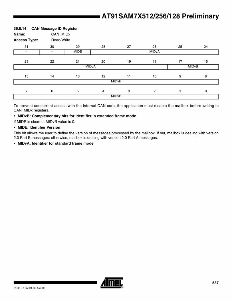
AT91SAM7X512/256/128 Preliminary
36.8.14 CAN Message ID Register
Name: CAN_MIDx
Access Type: Read/Write
To prevent concurrent access with the internal CAN core, the application must disable the mailbox before writing to CAN_MIDx registers.
• MIDvB: Complementary bits for identifier in extended frame mode
If MIDE is cleared, MIDvB value is 0.
• MIDE: Identifier Version
This bit allows the user to define the version of messages processed by the mailbox. If set, mailbox is dealing with version 2.0 Part B messages; otherwise, mailbox is dealing with version 2.0 Part A messages.
• MIDvA: Identifier for standard frame mode
31 30 29 28 27 26 25 24– – MIDE MIDvA
23 22 21 20 19 18 17 16
MIDvA MIDvB
15 14 13 12 11 10 9 8
MIDvB
7 6 5 4 3 2 1 0
MIDvB
5376120F–ATARM–03-Oct-06

AT91SAM7X512/256/128 Preliminary
36.8.15 CAN Message Family ID Register
Name: CAN_MFIDx
Access Type: Read-only
• MFID: Family ID
This field contains the concatenation of CAN_MIDx register bits masked by the CAN_MAMx register. This field is useful to speed up message ID decoding. The message acceptance procedure is described below.
As an example:CAN_MIDx = 0x305A4321
CAN_MAMx = 0x3FF0F0FF
CAN_MFIDx = 0x000000A3
31 30 29 28 27 26 25 24– – – MFID
23 22 21 20 19 18 17 16
MFID
15 14 13 12 11 10 9 8
MFID
7 6 5 4 3 2 1 0
MFID
5386120F–ATARM–03-Oct-06

AT91SAM7X512/256/128 Preliminary
36.8.16 CAN Message Status Register
Name: CAN_MSRx
Access Type: Read only
These register fields are updated each time a message transfer is received or aborted.
MMI is cleared by reading the CAN_MSRx register.
MRDY, MABT are cleared by writing MTCR or MACR in the CAN_MCRx register.
Warning: MRTR and MDLC state depends partly on the mailbox object type.
• MTIMESTAMP: Timer value
This field is updated only when time-triggered operations are disabled (TTM cleared in CAN_MR register). If the TEOF field in the CAN_MR register is cleared, TIMESTAMP is the internal timer value at the start of frame of the last message received or sent by the mailbox. If the TEOF field in the CAN_MR register is set, TIMESTAMP is the internal timer value at the end of frame of the last message received or sent by the mailbox.
In Time Triggered Mode, MTIMESTAMP is set to 0.
• MDLC: Mailbox Data Length Code
31 30 29 28 27 26 25 24– – – – – – – MMI
23 22 21 20 19 18 17 16
MRDY MABT – MRTR MDLC
15 14 13 12 11 10 9 8
MTIMESTAMP15
MTIMESTAMP14
MTIMESTAMP13
MTIMESTAMP12
MTIMESTAMP11
MTIMESTAMP10
MTIMESTAMP9
MTIMESTAMP8
7 6 5 4 3 2 1 0
MTIMESTAMP7
MTIMESTAMP6
MTIMESTAMP5
MTIMESTAMP4
MTIMESTAMP3
MTIMESTAMP2
MTIMESTAMP1
MTIMESTAMP0
Mailbox Object Type Description
Receive Length of the first mailbox message received
Receive with overwrite Length of the last mailbox message received
Transmit No action
Consumer Length of the mailbox message received
Producer Length of the mailbox message to be sent after the remote frame reception
5396120F–ATARM–03-Oct-06
AT91SAM7X512/256/128 Preliminary
• MRTR: Mailbox Remote Transmission Request
• MABT: Mailbox Message Abort
An interrupt is triggered when MABT is set.
0 = Previous transfer is not aborted.
1 = Previous transfer has been aborted.
This flag is cleared by writing to CAN_MCRx register
Mailbox Object Type Description
Receive The first frame received has the RTR bit set.
Receive with overwrite The last frame received has the RTR bit set.
Transmit Reserved
Consumer Reserved. After setting the MOT field in the CAN_MMR, MRTR is reset to 1.
Producer Reserved. After setting the MOT field in the CAN_MMR, MRTR is reset to 0.
Mailbox Object Type Description
Receive Reserved
Receive with overwrite Reserved
Transmit Previous transfer has been aborted
Consumer The remote frame transfer request has been aborted.
Producer The response to the remote frame transfer has been aborted.
5406120F–ATARM–03-Oct-06

AT91SAM7X512/256/128 Preliminary
• MRDY: Mailbox Ready
An interrupt is triggered when MRDY is set.
0 = Mailbox data registers can not be read/written by the software application. CAN_MDx are locked by the CAN_MDx.
1 = Mailbox data registers can be read/written by the software application.
This flag is cleared by writing to CAN_MCRx register.
• MMI: Mailbox Message Ignored
0 = No message has been ignored during the previous transfer
1 = At least one message has been ignored during the previous transfer
Cleared by reading the CAN_MSRx register.
Mailbox Object Type Description
ReceiveAt least one message has been received since the last mailbox transfer order. Data from the first frame received can be read in the CAN_MDxx registers.
After setting the MOT field in the CAN_MMR, MRDY is reset to 0.
Receive with overwriteAt least one frame has been received since the last mailbox transfer order. Data from the last frame received can be read in the CAN_MDxx registers.After setting the MOT field in the CAN_MMR, MRDY is reset to 0.
TransmitMailbox data have been transmitted.After setting the MOT field in the CAN_MMR, MRDY is reset to 1.
ConsumerAt least one message has been received since the last mailbox transfer order. Data from the first message received can be read in the CAN_MDxx registers.
After setting the MOT field in the CAN_MMR, MRDY is reset to 0.
ProducerA remote frame has been received, mailbox data have been transmitted.
After setting the MOT field in the CAN_MMR, MRDY is reset to 1.
Mailbox Object Type Description
ReceiveSet when at least two messages intended for the mailbox have been sent. The first one is available in the mailbox data register. Others have been ignored. A mailbox with a lower priority may have accepted the message.
Receive with overwriteSet when at least two messages intended for the mailbox have been sent. The last one is available in the mailbox data register. Previous ones have been lost.
Transmit Reserved
ConsumerA remote frame has been sent by the mailbox but several messages have been received. The first one is available in the mailbox data register. Others have been ignored. Another mailbox with a lower priority may have accepted the message.
Producer A remote frame has been received, but no data are available to be sent.
5416120F–ATARM–03-Oct-06

AT91SAM7X512/256/128 Preliminary
36.8.17 CAN Message Data Low Register
Name: CAN_MDLx
Access Type: Read/Write
• MDL: Message Data Low Value
When MRDY field is set in the CAN_MSRx register, the lower 32 bits of a received message can be read or written by the software application. Otherwise, the MDL value is locked by the CAN controller to send/receive a new message.
In Receive with overwrite, the CAN controller may modify MDL value while the software application reads MDH and MDL registers. To check that MDH and MDL do not belong to different messages, the application has to check the MMI field in the CAN_MSRx register. In this mode, the software application must re-read CAN_MDH and CAN_MDL, while the MMI bit in the CAN_MSRx register is set.
Bytes are received/sent on the bus in the following order:
1. CAN_MDL[7:0]
2. CAN_MDL[15:8]
3. CAN_MDL[23:16]
4. CAN_MDL[31:24]
5. CAN_MDH[7:0]
6. CAN_MDH[15:8]
7. CAN_MDH[23:16]
8. CAN_MDH[31:24]
31 30 29 28 27 26 25 24
MDL
23 22 21 20 19 18 17 16
MDL
15 14 13 12 11 10 9 8
MDL
7 6 5 4 3 2 1 0
MDL
5426120F–ATARM–03-Oct-06
AT91SAM7X512/256/128 Preliminary
36.8.18 CAN Message Data High Register
Name: CAN_MDHx
Access Type: Read/Write
• MDH: Message Data High Value
When MRDY field is set in the CAN_MSRx register, the upper 32 bits of a received message are read or written by the soft-ware application. Otherwise, the MDH value is locked by the CAN controller to send/receive a new message.
In Receive with overwrite, the CAN controller may modify MDH value while the software application reads MDH and MDL registers. To check that MDH and MDL do not belong to different messages, the application has to check the MMI field in the CAN_MSRx register. In this mode, the software application must re-read CAN_MDH and CAN_MDL, while the MMI bit in the CAN_MSRx register is set.
Bytes are received/sent on the bus in the following order:
1. CAN_MDL[7:0]
2. CAN_MDL[15:8]
3. CAN_MDL[23:16]
4. CAN_MDL[31:24]
5. CAN_MDH[7:0]
6. CAN_MDH[15:8]
7. CAN_MDH[23:16]
8. CAN_MDH[31:24]
31 30 29 28 27 26 25 24
MDH
23 22 21 20 19 18 17 16
MDH
15 14 13 12 11 10 9 8
MDH
7 6 5 4 3 2 1 0
MDH
5436120F–ATARM–03-Oct-06
AT91SAM7X512/256/128 Preliminary
36.8.19 CAN Message Control Register
Name: CAN_MCRx
Access Type: Write-only
• MDLC: Mailbox Data Length Code
• MRTR: Mailbox Remote Transmission Request
Consumer situations can be handled automatically by setting the mailbox object type in Consumer. This requires only one mailbox.
It can also be handled using two mailboxes, one in reception, the other in transmission. The MRTR and the MTCR bits must be set in the same time.
31 30 29 28 27 26 25 24– – – – – – – –
23 22 21 20 19 18 17 16
MTCR MACR – MRTR MDLC
15 14 13 12 11 10 9 8
– – – – – – – –
7 6 5 4 3 2 1 0
– – – – – – – –
Mailbox Object Type Description
Receive No action.
Receive with overwrite No action.
Transmit Length of the mailbox message.
Consumer No action.
Producer Length of the mailbox message to be sent after the remote frame reception.
Mailbox Object Type Description
Receive No action
Receive with overwrite No action
Transmit Set the RTR bit in the sent frame
Consumer No action, the RTR bit in the sent frame is set automatically
Producer No action
5446120F–ATARM–03-Oct-06

AT91SAM7X512/256/128 Preliminary
• MACR: Abort Request for Mailbox x
It is possible to set MACR field for several mailboxes in the same time, setting several bits to the CAN_ACR register.
• MTCR: Mailbox Transfer Command
This flag clears the MRDY and MABT flags in the CAN_MSRx register.
When several mailboxes are requested to be transmitted simultaneously, they are transmitted in turn. The mailbox with the highest priority is serviced first. If several mailboxes have the same priority, the mailbox with the lowest number is serviced first (i.e., MBx0 will be serviced before MBx 15 if they have the same priority).
It is possible to set MTCR for several mailboxes at the same time by writing to the CAN_TCR register.
Mailbox Object Type Description
Receive No action
Receive with overwrite No action
TransmitCancels transfer request if the message has not been transmitted to the CAN transceiver.
Consumer Cancels the current transfer before the remote frame has been sent.
Producer Cancels the current transfer. The next remote frame will not be serviced.
Mailbox Object Type Description
Receive Allows the reception of the next message.
Receive with overwrite Triggers a new reception.
Transmit Sends data prepared in the mailbox as soon as possible.
Consumer Sends a remote transmission frame.
ProducerSends data prepared in the mailbox after receiving a remote frame from a Consumer.
5456120F–ATARM–03-Oct-06

5466120F–ATARM–03-Oct-06
AT91SAM7X512/256/128 Preliminary

AT91SAM7X512/256/128 Preliminary
37. Ethernet MAC 10/100 (EMAC)
37.1 Overview
The EMAC module implements a 10/100 Ethernet MAC compatible with the IEEE 802.3 stan-dard using an address checker, statistics and control registers, receive and transmit blocks, and a DMA interface.
The address checker recognizes four specific 48-bit addresses and contains a 64-bit hash regis-ter for matching multicast and unicast addresses. It can recognize the broadcast address of all ones, copy all frames, and act on an external address match signal.
The statistics register block contains registers for counting various types of event associated with transmit and receive operations. These registers, along with the status words stored in the receive buffer list, enable software to generate network management statistics compatible with IEEE 802.3.
37.2 Block Diagram
Figure 37-1. EMAC Block Diagram
APBSlave
Register Interface
DMA Interface
Address Checker
Statistics Registers
Control Registers
Ethernet Receive
Ethernet Transmit
MDIO
MII/RMII
RX FIFO TX FIFO
ASBMaster
5476120F–ATARM–03-Oct-06
37.3 Functional Description
Figure 37-1 illustrates the different blocks of the EMAC module.
The control registers drive the MDIO interface, setup up DMA activity, start frame transmission and select modes of operation such as full- or half-duplex.
The receive block checks for valid preamble, FCS, alignment and length, and presents received frames to the address checking block and DMA interface.
The transmit block takes data from the DMA interface, adds preamble and, if necessary, pad and FCS, and transmits data according to the CSMA/CD (carrier sense multiple access with col-lision detect) protocol. The start of transmission is deferred if CRS (carrier sense) is active.
If COL (collision) becomes active during transmission, a jam sequence is asserted and the transmission is retried after a random back off. CRS and COL have no effect in full duplex mode.
The DMA block connects to external memory through its ASB bus interface. It contains receive and transmit FIFOs for buffering frame data. It loads the transmit FIFO and empties the receive FIFO using ASB bus master operations. Receive data is not sent to memory until the address checking logic has determined that the frame should be copied. Receive or transmit frames are stored in one or more buffers. Receive buffers have a fixed length of 128 bytes. Transmit buffers range in length between 0 and 2047 bytes, and up to 128 buffers are permitted per frame. The DMA block manages the transmit and receive framebuffer queues. These queues can hold mul-tiple frames.
37.3.1 Memory Interface
Frame data is transferred to and from the EMAC through the DMA interface. All transfers are 32-bit words and may be single accesses or bursts of 2, 3 or 4 words. Burst accesses do not cross sixteen-byte boundaries. Bursts of 4 words are the default data transfer; single accesses or bursts of less than four words may be used to transfer data at the beginning or the end of a buffer.
The DMA controller performs six types of operation on the bus. In order of priority, these are:
1. Receive buffer manager write
2. Receive buffer manager read
3. Transmit data DMA read
4. Receive data DMA write
5. Transmit buffer manager read
6. Transmit buffer manager write
37.3.1.1 FIFO
The FIFO depths are 28 bytes and 28 bytes and area function of the system clock speed, mem-ory latency and network speed.
Data is typically transferred into and out of the FIFOs in bursts of four words. For receive, a bus request is asserted when the FIFO contains four words and has space for three more. For trans-mit, a bus request is generated when there is space for four words, or when there is space for two words if the next transfer is to be only one or two words.
Thus the bus latency must be less than the time it takes to load the FIFO and transmit or receive three words (12 bytes) of data.
5486120F–ATARM–03-Oct-06
AT91SAM7X512/256/128 Preliminary
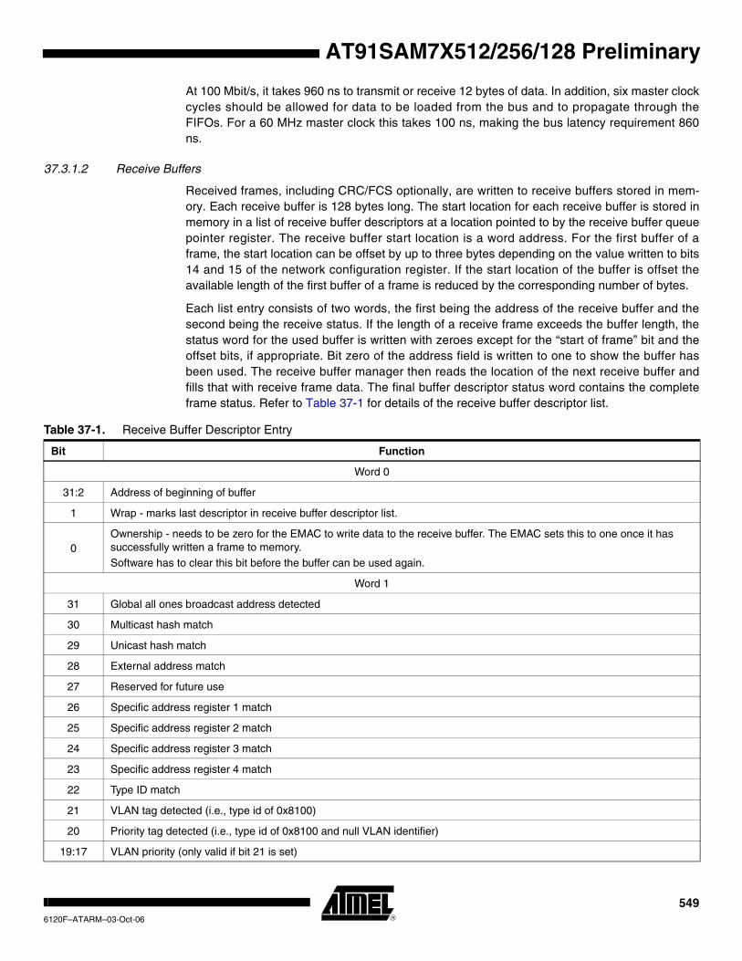
AT91SAM7X512/256/128 Preliminary
At 100 Mbit/s, it takes 960 ns to transmit or receive 12 bytes of data. In addition, six master clock cycles should be allowed for data to be loaded from the bus and to propagate through the FIFOs. For a 60 MHz master clock this takes 100 ns, making the bus latency requirement 860 ns.
37.3.1.2 Receive Buffers
Received frames, including CRC/FCS optionally, are written to receive buffers stored in mem-ory. Each receive buffer is 128 bytes long. The start location for each receive buffer is stored in memory in a list of receive buffer descriptors at a location pointed to by the receive buffer queue pointer register. The receive buffer start location is a word address. For the first buffer of a frame, the start location can be offset by up to three bytes depending on the value written to bits 14 and 15 of the network configuration register. If the start location of the buffer is offset the available length of the first buffer of a frame is reduced by the corresponding number of bytes.
Each list entry consists of two words, the first being the address of the receive buffer and the second being the receive status. If the length of a receive frame exceeds the buffer length, the status word for the used buffer is written with zeroes except for the “start of frame” bit and the offset bits, if appropriate. Bit zero of the address field is written to one to show the buffer has been used. The receive buffer manager then reads the location of the next receive buffer and fills that with receive frame data. The final buffer descriptor status word contains the complete frame status. Refer to Table 37-1 for details of the receive buffer descriptor list.
Table 37-1. Receive Buffer Descriptor Entry
Bit Function
Word 0
31:2 Address of beginning of buffer
1 Wrap - marks last descriptor in receive buffer descriptor list.
0Ownership - needs to be zero for the EMAC to write data to the receive buffer. The EMAC sets this to one once it has successfully written a frame to memory. Software has to clear this bit before the buffer can be used again.
Word 1
31 Global all ones broadcast address detected
30 Multicast hash match
29 Unicast hash match
28 External address match
27 Reserved for future use
26 Specific address register 1 match
25 Specific address register 2 match
24 Specific address register 3 match
23 Specific address register 4 match
22 Type ID match
21 VLAN tag detected (i.e., type id of 0x8100)
20 Priority tag detected (i.e., type id of 0x8100 and null VLAN identifier)
19:17 VLAN priority (only valid if bit 21 is set)
5496120F–ATARM–03-Oct-06
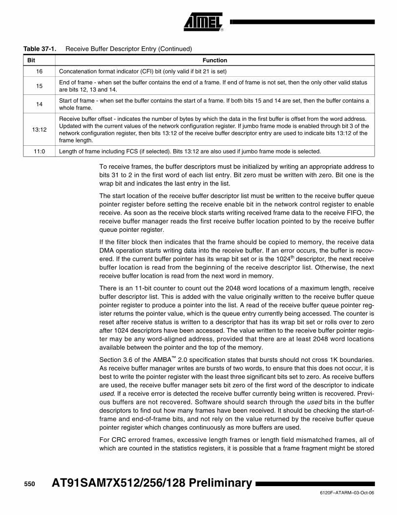
To receive frames, the buffer descriptors must be initialized by writing an appropriate address to bits 31 to 2 in the first word of each list entry. Bit zero must be written with zero. Bit one is the wrap bit and indicates the last entry in the list.
The start location of the receive buffer descriptor list must be written to the receive buffer queue pointer register before setting the receive enable bit in the network control register to enable receive. As soon as the receive block starts writing received frame data to the receive FIFO, the receive buffer manager reads the first receive buffer location pointed to by the receive buffer queue pointer register.
If the filter block then indicates that the frame should be copied to memory, the receive data DMA operation starts writing data into the receive buffer. If an error occurs, the buffer is recov-ered. If the current buffer pointer has its wrap bit set or is the 1024th descriptor, the next receive buffer location is read from the beginning of the receive descriptor list. Otherwise, the next receive buffer location is read from the next word in memory.
There is an 11-bit counter to count out the 2048 word locations of a maximum length, receive buffer descriptor list. This is added with the value originally written to the receive buffer queue pointer register to produce a pointer into the list. A read of the receive buffer queue pointer reg-ister returns the pointer value, which is the queue entry currently being accessed. The counter is reset after receive status is written to a descriptor that has its wrap bit set or rolls over to zero after 1024 descriptors have been accessed. The value written to the receive buffer pointer regis-ter may be any word-aligned address, provided that there are at least 2048 word locations available between the pointer and the top of the memory.
Section 3.6 of the AMBA™ 2.0 specification states that bursts should not cross 1K boundaries. As receive buffer manager writes are bursts of two words, to ensure that this does not occur, it is best to write the pointer register with the least three significant bits set to zero. As receive buffers are used, the receive buffer manager sets bit zero of the first word of the descriptor to indicate used. If a receive error is detected the receive buffer currently being written is recovered. Previ-ous buffers are not recovered. Software should search through the used bits in the buffer descriptors to find out how many frames have been received. It should be checking the start-of-frame and end-of-frame bits, and not rely on the value returned by the receive buffer queue pointer register which changes continuously as more buffers are used.
For CRC errored frames, excessive length frames or length field mismatched frames, all of which are counted in the statistics registers, it is possible that a frame fragment might be stored
16 Concatenation format indicator (CFI) bit (only valid if bit 21 is set)
15End of frame - when set the buffer contains the end of a frame. If end of frame is not set, then the only other valid status are bits 12, 13 and 14.
14Start of frame - when set the buffer contains the start of a frame. If both bits 15 and 14 are set, then the buffer contains a whole frame.
13:12
Receive buffer offset - indicates the number of bytes by which the data in the first buffer is offset from the word address. Updated with the current values of the network configuration register. If jumbo frame mode is enabled through bit 3 of the network configuration register, then bits 13:12 of the receive buffer descriptor entry are used to indicate bits 13:12 of the frame length.
11:0 Length of frame including FCS (if selected). Bits 13:12 are also used if jumbo frame mode is selected.
Table 37-1. Receive Buffer Descriptor Entry (Continued)
Bit Function
5506120F–ATARM–03-Oct-06
AT91SAM7X512/256/128 Preliminary
AT91SAM7X512/256/128 Preliminary
in a sequence of receive buffers. Software can detect this by looking for start of frame bit set in a buffer following a buffer with no end of frame bit set.
For a properly working Ethernet system, there should be no excessively long frames or frames greater than 128 bytes with CRC/FCS errors. Collision fragments are less than 128 bytes long. Therefore, it is a rare occurrence to find a frame fragment in a receive buffer.
If bit zero is set when the receive buffer manager reads the location of the receive buffer, then the buffer has already been used and cannot be used again until software has processed the frame and cleared bit zero. In this case, the DMA block sets the buffer not available bit in the receive status register and triggers an interrupt.
If bit zero is set when the receive buffer manager reads the location of the receive buffer and a frame is being received, the frame is discarded and the receive resource error statistics register is incremented.
A receive overrun condition occurs when bus was not granted in time or because HRESP was not OK (bus error). In a receive overrun condition, the receive overrun interrupt is asserted and the buffer currently being written is recovered. The next frame received with an address that is recognized reuses the buffer.
If bit 17 of the network configuration register is set, the FCS of received frames shall not be cop-ied to memory. The frame length indicated in the receive status field shall be reduced by four bytes in this case.
37.3.1.3 Transmit Buffer
Frames to be transmitted are stored in one or more transmit buffers. Transmit buffers can be between 0 and 2047 bytes long, so it is possible to transmit frames longer than the maximum length specified in IEEE Standard 802.3. Zero length buffers are allowed. The maximum number of buffers permitted for each transmit frame is 128.
The start location for each transmit buffer is stored in memory in a list of transmit buffer descrip-tors at a location pointed to by the transmit buffer queue pointer register. Each list entry consists of two words, the first being the byte address of the transmit buffer and the second containing the transmit control and status. Frames can be transmitted with or without automatic CRC gen-eration. If CRC is automatically generated, pad is also automatically generated to take frames to a minimum length of 64 bytes. Table 37-2 on page 552 defines an entry in the transmit buffer descriptor list. To transmit frames, the buffer descriptors must be initialized by writing an appro-priate byte address to bits 31 to 0 in the first word of each list entry. The second transmit buffer descriptor is initialized with control information that indicates the length of the buffer, whether or not it is to be transmitted with CRC and whether the buffer is the last buffer in the frame.
After transmission, the control bits are written back to the second word of the first buffer along with the “used” bit and other status information. Bit 31 is the “used” bit which must be zero when the control word is read if transmission is to happen. It is written to one when a frame has been transmitted. Bits 27, 28 and 29 indicate various transmit error conditions. Bit 30 is the “wrap” bit which can be set for any buffer within a frame. If no wrap bit is encountered after 1024 descrip-tors, the queue pointer rolls over to the start in a similar fashion to the receive queue.
The transmit buffer queue pointer register must not be written while transmit is active. If a new value is written to the transmit buffer queue pointer register, the queue pointer resets itself to point to the beginning of the new queue. If transmit is disabled by writing to bit 3 of the network control, the transmit buffer queue pointer register resets to point to the beginning of the transmit queue. Note that disabling receive does not have the same effect on the receive queue pointer.
5516120F–ATARM–03-Oct-06

Once the transmit queue is initialized, transmit is activated by writing to bit 9, the Transmit Start bit of the network control register. Transmit is halted when a buffer descriptor with its used bit set is read, or if a transmit error occurs, or by writing to the transmit halt bit of the network control register. (Transmission is suspended if a pause frame is received while the pause enable bit is set in the network configuration register.) Rewriting the start bit while transmission is active is allowed.
Transmission control is implemented with a Tx_go variable which is readable in the transmit sta-tus register at bit location 3. The Tx_go variable is reset when:
– transmit is disabled
– a buffer descriptor with its ownership bit set is read
– a new value is written to the transmit buffer queue pointer register
– bit 10, tx_halt, of the network control register is written
– there is a transmit error such as too many retries or a transmit underrun.
To set tx_go, write to bit 9, tx_start, of the network control register. Transmit halt does not take effect until any ongoing transmit finishes. If a collision occurs during transmission of a multi-buffer frame, transmission automatically restarts from the first buffer of the frame. If a “used” bit is read midway through transmission of a multi-buffer frame, this is treated as a transmit error. Transmission stops, tx_er is asserted and the FCS is bad.
If transmission stops due to a transmit error, the transmit queue pointer resets to point to the beginning of the transmit queue. Software needs to re-initialize the transmit queue after a trans-mit error.
If transmission stops due to a “used” bit being read at the start of the frame, the transmission queue pointer is not reset and transmit starts from the same transmit buffer descriptor when the transmit start bit is written
Table 37-2. Transmit Buffer Descriptor Entry
Bit Function
Word 0
31:0 Byte Address of buffer
Word 1
31
Used. Needs to be zero for the EMAC to read data from the transmit buffer. The EMAC sets this to one for the first buffer of a frame once it has been successfully transmitted.
Software has to clear this bit before the buffer can be used again.
Note: This bit is only set for the first buffer in a frame unlike receive where all buffers have the Used bit set once used.
30 Wrap. Marks last descriptor in transmit buffer descriptor list.
29 Retry limit exceeded, transmit error detected
28Transmit underrun, occurs either when hresp is not OK (bus error) or the transmit data could not be fetched in time or when buffers are exhausted in mid frame.
27 Buffers exhausted in mid frame
26:17 Reserved
16 No CRC. When set, no CRC is appended to the current frame. This bit only needs to be set for the last buffer of a frame.
15 Last buffer. When set, this bit indicates the last buffer in the current frame has been reached.
14:11 Reserved
10:0 Length of buffer
5526120F–ATARM–03-Oct-06
AT91SAM7X512/256/128 Preliminary
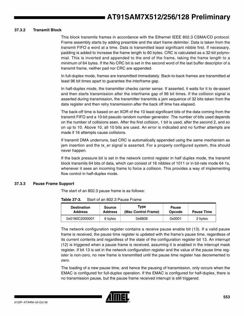
AT91SAM7X512/256/128 Preliminary
37.3.2 Transmit Block
This block transmits frames in accordance with the Ethernet IEEE 802.3 CSMA/CD protocol. Frame assembly starts by adding preamble and the start frame delimiter. Data is taken from the transmit FIFO a word at a time. Data is transmitted least significant nibble first. If necessary, padding is added to increase the frame length to 60 bytes. CRC is calculated as a 32-bit polyno-mial. This is inverted and appended to the end of the frame, taking the frame length to a minimum of 64 bytes. If the No CRC bit is set in the second word of the last buffer descriptor of a transmit frame, neither pad nor CRC are appended.
In full-duplex mode, frames are transmitted immediately. Back-to-back frames are transmitted at least 96 bit times apart to guarantee the interframe gap.
In half-duplex mode, the transmitter checks carrier sense. If asserted, it waits for it to de-assert and then starts transmission after the interframe gap of 96 bit times. If the collision signal is asserted during transmission, the transmitter transmits a jam sequence of 32 bits taken from the data register and then retry transmission after the back off time has elapsed.
The back-off time is based on an XOR of the 10 least significant bits of the data coming from the transmit FIFO and a 10-bit pseudo random number generator. The number of bits used depends on the number of collisions seen. After the first collision, 1 bit is used, after the second 2, and so on up to 10. Above 10, all 10 bits are used. An error is indicated and no further attempts are made if 16 attempts cause collisions.
If transmit DMA underruns, bad CRC is automatically appended using the same mechanism as jam insertion and the tx_er signal is asserted. For a properly configured system, this should never happen.
If the back pressure bit is set in the network control register in half duplex mode, the transmit block transmits 64 bits of data, which can consist of 16 nibbles of 1011 or in bit-rate mode 64 1s, whenever it sees an incoming frame to force a collision. This provides a way of implementing flow control in half-duplex mode.
37.3.3 Pause Frame Support
The start of an 802.3 pause frame is as follows:
The network configuration register contains a receive pause enable bit (13). If a valid pause frame is received, the pause time register is updated with the frame’s pause time, regardless of its current contents and regardless of the state of the configuration register bit 13. An interrupt (12) is triggered when a pause frame is received, assuming it is enabled in the interrupt mask register. If bit 13 is set in the network configuration register and the value of the pause time reg-ister is non-zero, no new frame is transmitted until the pause time register has decremented to zero.
The loading of a new pause time, and hence the pausing of transmission, only occurs when the EMAC is configured for full-duplex operation. If the EMAC is configured for half-duplex, there is no transmission pause, but the pause frame received interrupt is still triggered.
Table 37-3. Start of an 802.3 Pause Frame
Destination Address
Source Address
Type(Mac Control Frame)
Pause Opcode Pause Time
0x0180C2000001 6 bytes 0x8808 0x0001 2 bytes
5536120F–ATARM–03-Oct-06

A valid pause frame is defined as having a destination address that matches either the address stored in specific address register 1 or matches 0x0180C2000001 and has the MAC control frame type ID of 0x8808 and the pause opcode of 0x0001. Pause frames that have FCS or other errors are treated as invalid and are discarded. Valid pause frames received increment the Pause Frame Received statistic register.
The pause time register decrements every 512 bit times (i.e., 128 rx_clks in nibble mode) once transmission has stopped. For test purposes, the register decrements every rx_clk cycle once transmission has stopped if bit 12 (retry test) is set in the network configuration register. If the pause enable bit (13) is not set in the network configuration register, then the decrementing occurs regardless of whether transmission has stopped or not.
An interrupt (13) is asserted whenever the pause time register decrements to zero (assuming it is enabled in the interrupt mask register).
37.3.4 Receive Block
The receive block checks for valid preamble, FCS, alignment and length, presents received frames to the DMA block and stores the frames destination address for use by the address checking block. If, during frame reception, the frame is found to be too long or rx_er is asserted, a bad frame indication is sent to the DMA block. The DMA block then ceases sending data to memory. At the end of frame reception, the receive block indicates to the DMA block whether the frame is good or bad. The DMA block recovers the current receive buffer if the frame was bad. The receive block signals the register block to increment the alignment error, the CRC (FCS) error, the short frame, long frame, jabber error, the receive symbol error statistics and the length field mismatch statistics.
The enable bit for jumbo frames in the network configuration register allows the EMAC to receive jumbo frames of up to 10240 bytes in size. This operation does not form part of the IEEE802.3 specification and is disabled by default. When jumbo frames are enabled, frames received with a frame size greater than 10240 bytes are discarded.
37.3.5 Address Checking Block
The address checking (or filter) block indicates to the DMA block which receive frames should be copied to memory. Whether a frame is copied depends on what is enabled in the network configuration register, the state of the external match pin, the contents of the specific address and hash registers and the frame’s destination address. In this implementation of the EMAC, the frame’s source address is not checked. Provided that bit 18 of the Network Configuration regis-ter is not set, a frame is not copied to memory if the EMAC is transmitting in half duplex mode at the time a destination address is received. If bit 18 of the Network Configuration register is set, frames can be received while transmitting in half-duplex mode.
Ethernet frames are transmitted a byte at a time, least significant bit first. The first six bytes (48 bits) of an Ethernet frame make up the destination address. The first bit of the destination address, the LSB of the first byte of the frame, is the group/individual bit: this is One for multicast addresses and Zero for unicast. The All Ones address is the broadcast address, and a special case of multicast.
The EMAC supports recognition of four specific addresses. Each specific address requires two registers, specific address register bottom and specific address register top. Specific address register bottom stores the first four bytes of the destination address and specific address register top contains the last two bytes. The addresses stored can be specific, group, local or universal.
5546120F–ATARM–03-Oct-06
AT91SAM7X512/256/128 Preliminary
AT91SAM7X512/256/128 Preliminary
The destination address of received frames is compared against the data stored in the specific address registers once they have been activated. The addresses are deactivated at reset or when their corresponding specific address register bottom is written. They are activated when specific address register top is written. If a receive frame address matches an active address, the frame is copied to memory.
The following example illustrates the use of the address match registers for a MAC address of 21:43:65:87:A9:CB.
Preamble 55
SFD D5
DA (Octet0 - LSB) 21
DA(Octet 1) 43
DA(Octet 2) 65
DA(Octet 3) 87
DA(Octet 4) A9
DA (Octet5 - MSB) CB
SA (LSB) 00
SA 00
SA 00
SA 00
SA 00
SA (MSB) 43
SA (LSB) 21
The sequence above shows the beginning of an Ethernet frame. Byte order of transmission is from top to bottom as shown. For a successful match to specific address 1, the following address matching registers must be set up:
• Base address + 0x98 0x87654321 (Bottom)
• Base address + 0x9C 0x0000CBA9 (Top)
And for a successful match to the Type ID register, the following should be set up:
• Base address + 0xB8 0x00004321
37.3.6 Broadcast Address
The broadcast address of 0xFFFFFFFFFFFF is recognized if the ‘no broadcast’ bit in the net-work configuration register is zero.
37.3.7 Hash Addressing
The hash address register is 64 bits long and takes up two locations in the memory map. The least significant bits are stored in hash register bottom and the most significant bits in hash reg-ister top.
The unicast hash enable and the multicast hash enable bits in the network configuration register enable the reception of hash matched frames. The destination address is reduced to a 6-bit
5556120F–ATARM–03-Oct-06

index into the 64-bit hash register using the following hash function. The hash function is an exclusive or of every sixth bit of the destination address.
hash_index[5] = da[5] ^ da[11] ^ da[17] ^ da[23] ^ da[29] ^ da[35] ^ da[41] ^ da[47]
hash_index[4] = da[4] ^ da[10] ^ da[16] ^ da[22] ^ da[28] ^ da[34] ^ da[40] ^ da[46]
hash_index[3] = da[3] ^ da[09] ^ da[15] ^ da[21] ^ da[27] ^ da[33] ^ da[39] ^ da[45]
hash_index[2] = da[2] ^ da[08] ^ da[14] ^ da[20] ^ da[26] ^ da[32] ^ da[38] ^ da[44]
hash_index[1] = da[1] ^ da[07] ^ da[13] ^ da[19] ^ da[25] ^ da[31] ^ da[37] ^ da[43]
hash_index[0] = da[0] ^ da[06] ^ da[12] ^ da[18] ^ da[24] ^ da[30] ^ da[36] ^ da[42]
da[0] represents the least significant bit of the first byte received, that is, the multicast/unicast indicator, and da[47] represents the most significant bit of the last byte received.
If the hash index points to a bit that is set in the hash register, then the frame is matched accord-ing to whether the frame is multicast or unicast.
A multicast match is signalled if the multicast hash enable bit is set. da[0] is 1 and the hash index points to a bit set in the hash register.
A unicast match is signalled if the unicast hash enable bit is set. da[0] is 0 and the hash index points to a bit set in the hash register.
To receive all multicast frames, the hash register should be set with all ones and the multicast hash enable bit should be set in the network configuration register.
37.3.8 Copy All Frames (or Promiscuous Mode)
If the copy all frames bit is set in the network configuration register, then all non-errored frames are copied to memory. For example, frames that are too long, too short, or have FCS errors or rx_er asserted during reception are discarded and all others are received. Frames with FCS errors are copied to memory if bit 19 in the network configuration register is set.
37.3.9 Type ID Checking
The contents of the type_id register are compared against the length/type ID of received frames (i.e., bytes 13 and 14). Bit 22 in the receive buffer descriptor status is set if there is a match. The reset state of this register is zero which is unlikely to match the length/type ID of any valid Ether-net frame.
Note: A type ID match does not affect whether a frame is copied to memory.
37.3.10 VLAN Support
An Ethernet encoded 802.1Q VLAN tag looks like this:
Table 37-4. 802.1Q VLAN Tag
TPID (Tag Protocol Identifier) 16 bits TCI (Tag Control Information) 16 bits
0x8100 First 3 bits priority, then CFI bit, last 12 bits VID
5566120F–ATARM–03-Oct-06
AT91SAM7X512/256/128 Preliminary

AT91SAM7X512/256/128 Preliminary
The VLAN tag is inserted at the 13th byte of the frame, adding an extra four bytes to the frame. If the VID (VLAN identifier) is null (0x000), this indicates a priority-tagged frame. The MAC can support frame lengths up to 1536 bytes, 18 bytes more than the original Ethernet maximum frame length of 1518 bytes. This is achieved by setting bit 8 in the network configuration register.
The following bits in the receive buffer descriptor status word give information about VLAN tagged frames:
• Bit 21 set if receive frame is VLAN tagged (i.e. type id of 0x8100)
• Bit 20 set if receive frame is priority tagged (i.e. type id of 0x8100 and null VID). (If bit 20 is set bit 21 is set also.)
• Bit 19, 18 and 17 set to priority if bit 21 is set
• Bit 16 set to CFI if bit 21 is set
37.3.11 PHY Maintenance
The register EMAC_MAN enables the EMAC to communicate with a PHY by means of the MDIO interface. It is used during auto-negotiation to ensure that the EMAC and the PHY are config-ured for the same speed and duplex configuration.
The PHY maintenance register is implemented as a shift register. Writing to the register starts a shift operation which is signalled as complete when bit two is set in the network status register (about 2000 MCK cycles later when bit ten is set to zero, and bit eleven is set to one in the net-work configuration register). An interrupt is generated as this bit is set. During this time, the MSB of the register is output on the MDIO pin and the LSB updated from the MDIO pin with each MDC cycle. This causes transmission of a PHY management frame on MDIO.
Reading during the shift operation returns the current contents of the shift register. At the end of management operation, the bits have shifted back to their original locations. For a read opera-tion, the data bits are updated with data read from the PHY. It is important to write the correct values to the register to ensure a valid PHY management frame is produced.
The MDIO interface can read IEEE 802.3 clause 45 PHYs as well as clause 22 PHYs. To read clause 45 PHYs, bits[31:28] should be written as 0x0011. For a description of MDC generation, see the network configuration register in the ”Network Control Register” on page 564.
37.3.12 Media Independent Interface
The Ethernet MAC is capable of interfacing to both RMII and MII Interfaces. The RMII bit in the EMAC_USRIO register controls the interface that is selected. When this bit is set, the RMII inter-face is selected, else the MII interface is selected.
The MII and RMII interface are capable of both 10Mb/s and 100Mb/s data rates as described in the IEEE 802.3u standard. The signals used by the MII and RMII interfaces are described in Table 37-5.
Table 37-5. Pin Configuration
Pin Name MII RMII
ETXCK_EREFCK ETXCK: Transmit Clock EREFCK: Reference Clock
ECRS ECRS: Carrier Sense
ECOL ECOL: Collision Detect
ERXDV ERXDV: Data Valid ECRSDV: Carrier Sense/Data Valid
5576120F–ATARM–03-Oct-06
The intent of the RMII is to provide a reduced pin count alternative to the IEEE 802.3u MII. It uses 2 bits for transmit (ETX0 and ETX1) and two bits for receive (ERX0 and ERX1). There is a Transmit Enable (ETXEN), a Receive Error (ERXER), a Carrier Sense (ECRS_DV), and a 50 MHz Reference Clock (ETXCK_EREFCK) for 100Mb/s data rate.
37.3.12.1 RMII Transmit and Receive Operation
The same signals are used internally for both the RMII and the MII operations. The RMII maps these signals in a more pin-efficient manner. The transmit and receive bits are converted from a 4-bit parallel format to a 2-bit parallel scheme that is clocked at twice the rate. The carrier sense and data valid signals are combined into the ECRSDV signal. This signal contains information on carrier sense, FIFO status, and validity of the data. Transmit error bit (ETXER) and collision detect (ECOL) are not used in RMII mode.
ERX0 - ERX3 ERX0 - ERX3: 4-bit Receive Data ERX0 - ERX1: 2-bit Receive Data
ERXER ERXER: Receive Error ERXER: Receive Error
ERXCK ERXCK: Receive Clock
ETXEN ETXEN: Transmit Enable ETXEN: Transmit Enable
ETX0-ETX3 ETX0 - ETX3: 4-bit Transmit Data ETX0 - ETX1: 2-bit Transmit Data
ETXER ETXER: Transmit Error
Table 37-5. Pin Configuration (Continued)
5586120F–ATARM–03-Oct-06
AT91SAM7X512/256/128 Preliminary

AT91SAM7X512/256/128 Preliminary
37.4 Programming Interface
37.4.1 Initialization
37.4.1.1 Configuration
Initialization of the EMAC configuration (e.g., loop-back mode, frequency ratios) must be done while the transmit and receive circuits are disabled. See the description of the network control register and network configuration register earlier in this document.
To change loop-back mode, the following sequence of operations must be followed:
1. Write to network control register to disable transmit and receive circuits.
2. Write to network control register to change loop-back mode.
3. Write to network control register to re-enable transmit or receive circuits.Note: These writes to network control register cannot be combined in any way.
37.4.1.2 Receive Buffer List
Receive data is written to areas of data (i.e., buffers) in system memory. These buffers are listed in another data structure that also resides in main memory. This data structure (receive buffer queue) is a sequence of descriptor entries as defined in ”Receive Buffer Descriptor Entry” on page 549. It points to this data structure.
Figure 37-2. Receive Buffer List
To create the list of buffers:
1. Allocate a number (n) of buffers of 128 bytes in system memory.
2. Allocate an area 2n words for the receive buffer descriptor entry in system memory and create n entries in this list. Mark all entries in this list as owned by EMAC, i.e., bit 0 of word 0 set to 0.
3. If less than 1024 buffers are defined, the last descriptor must be marked with the wrap bit (bit 1 in word 0 set to 1).
4. Write address of receive buffer descriptor entry to EMAC register receive_buffer queue pointer.
Receive Buffer Queue Pointer(MAC Register)
Receive Buffer 0
Receive Buffer 1
Receive Buffer N
Receive Buffer Descriptor List(In memory) (In memory)
5596120F–ATARM–03-Oct-06
5. The receive circuits can then be enabled by writing to the address recognition registers and then to the network control register.
37.4.1.3 Transmit Buffer List
Transmit data is read from areas of data (the buffers) in system memory These buffers are listed in another data structure that also resides in main memory. This data structure (Transmit Buffer Queue) is a sequence of descriptor entries (as defined in Table 37-2 on page 552) that points to this data structure.
To create this list of buffers:
1. Allocate a number (n) of buffers of between 1 and 2047 bytes of data to be transmitted in system memory. Up to 128 buffers per frame are allowed.
2. Allocate an area 2n words for the transmit buffer descriptor entry in system memory and create N entries in this list. Mark all entries in this list as owned by EMAC, i.e. bit 31 of word 1 set to 0.
3. If fewer than 1024 buffers are defined, the last descriptor must be marked with the wrap bit — bit 30 in word 1 set to 1.
4. Write address of transmit buffer descriptor entry to EMAC register transmit_buffer queue pointer.
5. The transmit circuits can then be enabled by writing to the network control register.
37.4.1.4 Address Matching
The EMAC register-pair hash address and the four specific address register-pairs must be writ-ten with the required values. Each register-pair comprises a bottom register and top register, with the bottom register being written first. The address matching is disabled for a particular reg-ister-pair after the bottom-register has been written and re-enabled when the top register is written. See “Address Checking Block” on page 554. for details of address matching. Each reg-ister-pair may be written at any time, regardless of whether the receive circuits are enabled or disabled.
37.4.1.5 Interrupts
There are 14 interrupt conditions that are detected within the EMAC. These are ORed to make a single interrupt. Depending on the overall system design, this may be passed through a further level of interrupt collection (interrupt controller). On receipt of the interrupt signal, the CPU enters the interrupt handler (Refer to the AIC programmer datasheet). To ascertain which inter-rupt has been generated, read the interrupt status register. Note that this register clears itself when read. At reset, all interrupts are disabled. To enable an interrupt, write to interrupt enable register with the pertinent interrupt bit set to 1. To disable an interrupt, write to interrupt disable register with the pertinent interrupt bit set to 1. To check whether an interrupt is enabled or dis-abled, read interrupt mask register: if the bit is set to 1, the interrupt is disabled.
37.4.1.6 Transmitting Frames
To set up a frame for transmission:
1. Enable transmit in the network control register.
2. Allocate an area of system memory for transmit data. This does not have to be contigu-ous, varying byte lengths can be used as long as they conclude on byte borders.
3. Set-up the transmit buffer list.
4. Set the network control register to enable transmission and enable interrupts.
5606120F–ATARM–03-Oct-06
AT91SAM7X512/256/128 Preliminary

AT91SAM7X512/256/128 Preliminary
5. Write data for transmission into these buffers.
6. Write the address to transmit buffer descriptor queue pointer.
7. Write control and length to word one of the transmit buffer descriptor entry.
8. Write to the transmit start bit in the network control register.
37.4.1.7 Receiving Frames
When a frame is received and the receive circuits are enabled, the EMAC checks the address and, in the following cases, the frame is written to system memory:
• if it matches one of the four specific address registers.
• if it matches the hash address function.
• if it is a broadcast address (0xFFFFFFFFFFFF) and broadcasts are allowed.
• if the EMAC is configured to copy all frames.
The register receive buffer queue pointer points to the next entry (see Table 37-1 on page 549) and the EMAC uses this as the address in system memory to write the frame to. Once the frame has been completely and successfully received and written to system memory, the EMAC then updates the receive buffer descriptor entry with the reason for the address match and marks the area as being owned by software. Once this is complete an interrupt receive complete is set. Software is then responsible for handling the data in the buffer and then releasing the buffer by writing the ownership bit back to 0.
If the EMAC is unable to write the data at a rate to match the incoming frame, then an interrupt receive overrun is set. If there is no receive buffer available, i.e., the next buffer is still owned by software, the interrupt receive buffer not available is set. If the frame is not successfully received, a statistic register is incremented and the frame is discarded without informing software.
5616120F–ATARM–03-Oct-06

37.5 Ethernet MAC 10/100 (EMAC) User Interface
Table 37-6. Ethernet MAC 10/100 (EMAC) Register Mapping
Offset Register Name Access Reset Value
0x00 Network Control Register EMAC_NCR Read/Write 0
0x04 Network Configuration Register EMAC_NCFG Read/Write 0x800
0x08 Network Status Register EMAC_NSR Read-only -
0x0C Reserved
0x10 Reserved
0x14 Transmit Status Register EMAC_TSR Read/Write 0x0000_0000
0x18 Receive Buffer Queue Pointer Register EMAC_RBQP Read/Write 0x0000_0000
0x1C Transmit Buffer Queue Pointer Register EMAC_TBQP Read/Write 0x0000_0000
0x20 Receive Status Register EMAC_RSR Read/Write 0x0000_0000
0x24 Interrupt Status Register EMAC_ISR Read/Write 0x0000_0000
0x28 Interrupt Enable Register EMAC_IER Write-only -
0x2C Interrupt Disable Register EMAC_IDR Write-only -
0x30 Interrupt Mask Register EMAC_IMR Read-only 0x0000_3FFF
0x34 Phy Maintenance Register EMAC_MAN Read/Write 0x0000_0000
0x38 Pause Time Register EMAC_PTR Read/Write 0x0000_0000
0x3C Pause Frames Received Register EMAC_PFR Read/Write 0x0000_0000
0x40 Frames Transmitted Ok Register EMAC_FTO Read/Write 0x0000_0000
0x44 Single Collision Frames Register EMAC_SCF Read/Write 0x0000_0000
0x48 Multiple Collision Frames Register EMAC_MCF Read/Write 0x0000_0000
0x4C Frames Received Ok Register EMAC_FRO Read/Write 0x0000_0000
0x50 Frame Check Sequence Errors Register EMAC_FCSE Read/Write 0x0000_0000
0x54 Alignment Errors Register EMAC_ALE Read/Write 0x0000_0000
0x58 Deferred Transmission Frames Register EMAC_DTF Read/Write 0x0000_0000
0x5C Late Collisions Register EMAC_LCOL Read/Write 0x0000_0000
0x60 Excessive Collisions Register EMAC_ECOL Read/Write 0x0000_0000
0x64 Transmit Underrun Errors Register EMAC_TUND Read/Write 0x0000_0000
0x68 Carrier Sense Errors Register EMAC_CSE Read/Write 0x0000_0000
0x6C Receive Resource Errors Register EMAC_RRE Read/Write 0x0000_0000
0x70 Receive Overrun Errors Register EMAC_ROV Read/Write 0x0000_0000
0x74 Receive Symbol Errors Register EMAC_RSE Read/Write 0x0000_0000
0x78 Excessive Length Errors Register EMAC_ELE Read/Write 0x0000_0000
0x7C Receive Jabbers Register EMAC_RJA Read/Write 0x0000_0000
0x80 Undersize Frames Register EMAC_USF Read/Write 0x0000_0000
0x84 SQE Test Errors Register EMAC_STE Read/Write 0x0000_0000
0x88 Received Length Field Mismatch Register EMAC_RLE Read/Write 0x0000_0000
5626120F–ATARM–03-Oct-06
AT91SAM7X512/256/128 Preliminary

AT91SAM7X512/256/128 Preliminary
0x90 Hash Register Bottom [31:0] Register EMAC_HRB Read/Write 0x0000_0000
0x94 Hash Register Top [63:32] Register EMAC_HRT Read/Write 0x0000_0000
0x98 Specific Address 1 Bottom Register EMAC_SA1B Read/Write 0x0000_0000
0x9C Specific Address 1 Top Register EMAC_SA1T Read/Write 0x0000_0000
0xA0 Specific Address 2 Bottom Register EMAC_SA2B Read/Write 0x0000_0000
0xA4 Specific Address 2 Top Register EMAC_SA2T Read/Write 0x0000_0000
0xA8 Specific Address 3 Bottom Register EMAC_SA3B Read/Write 0x0000_0000
0xAC Specific Address 3 Top Register EMAC_SA3T Read/Write 0x0000_0000
0xB0 Specific Address 4 Bottom Register EMAC_SA4B Read/Write 0x0000_0000
0xB4 Specific Address 4 Top Register EMAC_SA4T Read/Write 0x0000_0000
0xB8 Type ID Checking Register EMAC_TID Read/Write 0x0000_0000
0xC0 User Input/output Register EMAC_USRIO Read/Write 0x0000_0000
0xC8-0xF8 Reserved – – –
0xC8 - 0xFC Reserved – – –
Table 37-6. Ethernet MAC 10/100 (EMAC) Register Mapping (Continued)
Offset Register Name Access Reset Value
5636120F–ATARM–03-Oct-06

37.5.1 Network Control Register
Register Name: EMAC_NCR
Access Type: Read/Write
• LB: LoopBack
Asserts the loopback signal to the PHY.
• LLB: Loopback local
Connects txd to rxd, tx_en to rx_dv, forces full duplex and drives rx_clk and tx_clk with pclk divided by 4. rx_clk and tx_clk may glitch as the EMAC is switched into and out of internal loop back. It is important that receive and transmit circuits have already been disabled when making the switch into and out of internal loop back.
• RE: Receive enable
When set, enables the EMAC to receive data. When reset, frame reception stops immediately and the receive FIFO is cleared. The receive queue pointer register is unaffected.
• TE: Transmit enable
When set, enables the Ethernet transmitter to send data. When reset transmission, stops immediately, the transmit FIFO and control registers are cleared and the transmit queue pointer register resets to point to the start of the transmit descrip-tor list.
• MPE: Management port enable
Set to one to enable the management port. When zero, forces MDIO to high impedance state and MDC low.
• CLRSTAT: Clear statistics registers
This bit is write only. Writing a one clears the statistics registers.
• INCSTAT: Increment statistics registers
This bit is write only. Writing a one increments all the statistics registers by one for test purposes.
• WESTAT: Write enable for statistics registers
Setting this bit to one makes the statistics registers writable for functional test purposes.
• BP: Back pressure
If set in half duplex mode, forces collisions on all received frames.
• TSTART: Start transmission
Writing one to this bit starts transmission.
• THALT: Transmit halt
Writing one to this bit halts transmission as soon as any ongoing frame transmission ends.
31 30 29 28 27 26 25 24– – – – – – – –
23 22 21 20 19 18 17 16
– – – – – – – –
15 14 13 12 11 10 9 8
– – – – – THALT TSTART BP
7 6 5 4 3 2 1 0
WESTAT INCSTAT CLRSTAT MPE TE RE LLB LB
5646120F–ATARM–03-Oct-06
AT91SAM7X512/256/128 Preliminary
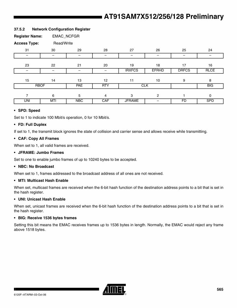
AT91SAM7X512/256/128 Preliminary
37.5.2 Network Configuration Register
Register Name: EMAC_NCFGR
Access Type: Read/Write
• SPD: Speed
Set to 1 to indicate 100 Mbit/s operation, 0 for 10 Mbit/s.
• FD: Full Duplex
If set to 1, the transmit block ignores the state of collision and carrier sense and allows receive while transmitting.
• CAF: Copy All Frames
When set to 1, all valid frames are received.
• JFRAME: Jumbo Frames
Set to one to enable jumbo frames of up to 10240 bytes to be accepted.
• NBC: No Broadcast
When set to 1, frames addressed to the broadcast address of all ones are not received.
• MTI: Multicast Hash Enable
When set, multicast frames are received when the 6-bit hash function of the destination address points to a bit that is set in the hash register.
• UNI: Unicast Hash Enable
When set, unicast frames are received when the 6-bit hash function of the destination address points to a bit that is set in the hash register.
• BIG: Receive 1536 bytes frames
Setting this bit means the EMAC receives frames up to 1536 bytes in length. Normally, the EMAC would reject any frame above 1518 bytes.
31 30 29 28 27 26 25 24– – – – – – – –
23 22 21 20 19 18 17 16
– – – – IRXFCS EFRHD DRFCS RLCE
15 14 13 12 11 10 9 8
RBOF PAE RTY CLK BIG
7 6 5 4 3 2 1 0
UNI MTI NBC CAF JFRAME – FD SPD
5656120F–ATARM–03-Oct-06

• CLK: MDC clock divider
Set according to system clock speed. This determines by what number system clock is divided to generate MDC. For conformance with 802.3, MDC must not exceed 2.5MHz (MDC is only active during MDIO read and write operations).
• RTY: Retry test
Must be set to zero for normal operation. If set to one, the back off between collisions is always one slot time. Setting this bit to one helps testing the too many retries condition. Also used in the pause frame tests to reduce the pause counters decrement time from 512 bit times, to every rx_clk cycle.
• PAE: Pause Enable
When set, transmission pauses when a valid pause frame is received.
• RBOF: Receive Buffer Offset
Indicates the number of bytes by which the received data is offset from the start of the first receive buffer.
• RLCE: Receive Length field Checking Enable
When set, frames with measured lengths shorter than their length fields are discarded. Frames containing a type ID in bytes 13 and 14 — length/type ID = 0600 — are not be counted as length errors.
• DRFCS: Discard Receive FCS
When set, the FCS field of received frames are not be copied to memory.
• EFRHD:
Enable Frames to be received in half-duplex mode while transmitting.
• IRXFCS: Ignore RX FCS
When set, frames with FCS/CRC errors are not rejected and no FCS error statistics are counted. For normal operation, this bit must be set to 0.
CLK MDC
00 MCK divided by 8 (MCK up to 20 MHz)
01 MCK divided by 16 (MCK up to 40 MHz)
10 MCK divided by 32 (MCK up to 80 MHz)
11 MCK divided by 64 (MCK up to 160 MHz)
RBOF Offset
00 No offset from start of receive buffer
01 One-byte offset from start of receive buffer
10 Two-byte offset from start of receive buffer
11 Three-byte offset from start of receive buffer
5666120F–ATARM–03-Oct-06
AT91SAM7X512/256/128 Preliminary

AT91SAM7X512/256/128 Preliminary
37.5.3 Network Status Register
Register Name: EMAC_NSR
Access Type: Read-only
• MDIO
Returns status of the MDIO pin. Use the PHY maintenance register for reading managed frames rather than this bit.
• IDLE
0 = The PHY management logic is idle (i.e., has completed).
1 = The PHY logic is running.
31 30 29 28 27 26 25 24– – – – – – – –
23 22 21 20 19 18 17 16
– – – – – – – –
15 14 13 12 11 10 9 8
– – – – – – – –
7 6 5 4 3 2 1 0
– – – – – IDLE MDIO –
5676120F–ATARM–03-Oct-06

37.5.4 Transmit Status Register
Register Name: EMAC_TSR
Access Type: Read/Write
This register, when read, provides details of the status of a transmit. Once read, individual bits may be cleared by writing 1 to them. It is not possible to set a bit to 1 by writing to the register.
• UBR: Used Bit Read
Set when a transmit buffer descriptor is read with its used bit set. Cleared by writing a one to this bit.
• COL: Collision Occurred
Set by the assertion of collision. Cleared by writing a one to this bit.
• RLE: Retry Limit exceeded
Cleared by writing a one to this bit.
• TGO: Transmit Go
If high transmit is active.
• BEX: Buffers exhausted mid frame
If the buffers run out during transmission of a frame, then transmission stops, FCS shall be bad and tx_er asserted. Cleared by writing a one to this bit.
• COMP: Transmit Complete
Set when a frame has been transmitted. Cleared by writing a one to this bit.
• UND: Transmit Underrun
Set when transmit DMA was not able to read data from memory, either because the bus was not granted in time, because a not OK hresp(bus error) was returned or because a used bit was read midway through frame transmission. If this occurs, the transmitter forces bad CRC. Cleared by writing a one to this bit.
31 30 29 28 27 26 25 24– – – – – – – –
23 22 21 20 19 18 17 16
– – – – – – – –
15 14 13 12 11 10 9 8
– – – – – – – –
7 6 5 4 3 2 1 0
– UND COMP BEX TGO RLE COL UBR
5686120F–ATARM–03-Oct-06
AT91SAM7X512/256/128 Preliminary

AT91SAM7X512/256/128 Preliminary
37.5.5 Receive Buffer Queue Pointer Register
Register Name: EMAC_RBQP
Access Type: Read/Write
This register points to the entry in the receive buffer queue (descriptor list) currently being used. It is written with the start location of the receive buffer descriptor list. The lower order bits increment as buffers are used up and wrap to their original values after either 1024 buffers or when the wrap bit of the entry is set.
Reading this register returns the location of the descriptor currently being accessed. This value increments as buffers are used. Software should not use this register for determining where to remove received frames from the queue as it con-stantly changes as new frames are received. Software should instead work its way through the buffer descriptor queue checking the used bits.
Receive buffer writes also comprise bursts of two words and, as with transmit buffer reads, it is recommended that bit 2 is always written with zero to prevent a burst crossing a 1K boundary, in violation of section 3.6 of the AMBA specification.
• ADDR: Receive buffer queue pointer address
Written with the address of the start of the receive queue, reads as a pointer to the current buffer being used.
31 30 29 28 27 26 25 24ADDR
23 22 21 20 19 18 17 16
ADDR
15 14 13 12 11 10 9 8
ADDR
7 6 5 4 3 2 1 0
ADDR – –
5696120F–ATARM–03-Oct-06

37.5.6 Transmit Buffer Queue Pointer Register
Register Name: EMAC_TBQP
Access Type: Read/Write
This register points to the entry in the transmit buffer queue (descriptor list) currently being used. It is written with the start location of the transmit buffer descriptor list. The lower order bits increment as buffers are used up and wrap to their original values after either 1024 buffers or when the wrap bit of the entry is set. This register can only be written when bit 3 in the transmit status register is low.
As transmit buffer reads consist of bursts of two words, it is recommended that bit 2 is always written with zero to prevent a burst crossing a 1K boundary, in violation of section 3.6 of the AMBA specification.
• ADDR: Transmit buffer queue pointer address
Written with the address of the start of the transmit queue, reads as a pointer to the first buffer of the frame being transmit-ted or about to be transmitted.
31 30 29 28 27 26 25 24ADDR
23 22 21 20 19 18 17 16
ADDR
15 14 13 12 11 10 9 8
ADDR
7 6 5 4 3 2 1 0
ADDR – –
5706120F–ATARM–03-Oct-06
AT91SAM7X512/256/128 Preliminary

AT91SAM7X512/256/128 Preliminary
37.5.7 Receive Status Register
Register Name: EMAC_RSR
Access Type: Read/Write
This register, when read, provides details of the status of a receive. Once read, individual bits may be cleared by writing 1 to them. It is not possible to set a bit to 1 by writing to the register.
• BNA: Buffer Not Available
An attempt was made to get a new buffer and the pointer indicated that it was owned by the processor. The DMA rereads the pointer each time a new frame starts until a valid pointer is found. This bit is set at each attempt that fails even if it has not had a successful pointer read since it has been cleared.
Cleared by writing a one to this bit.
• REC: Frame Received
One or more frames have been received and placed in memory. Cleared by writing a one to this bit.
• OVR: Receive Overrun
The DMA block was unable to store the receive frame to memory, either because the bus was not granted in time or because a not OK hresp(bus error) was returned. The buffer is recovered if this happens.
Cleared by writing a one to this bit.
31 30 29 28 27 26 25 24– – – – – – – –
23 22 21 20 19 18 17 16
– – – – – – – –
15 14 13 12 11 10 9 8
– – – – – – – –
7 6 5 4 3 2 1 0
– – – – – OVR REC BNA
5716120F–ATARM–03-Oct-06
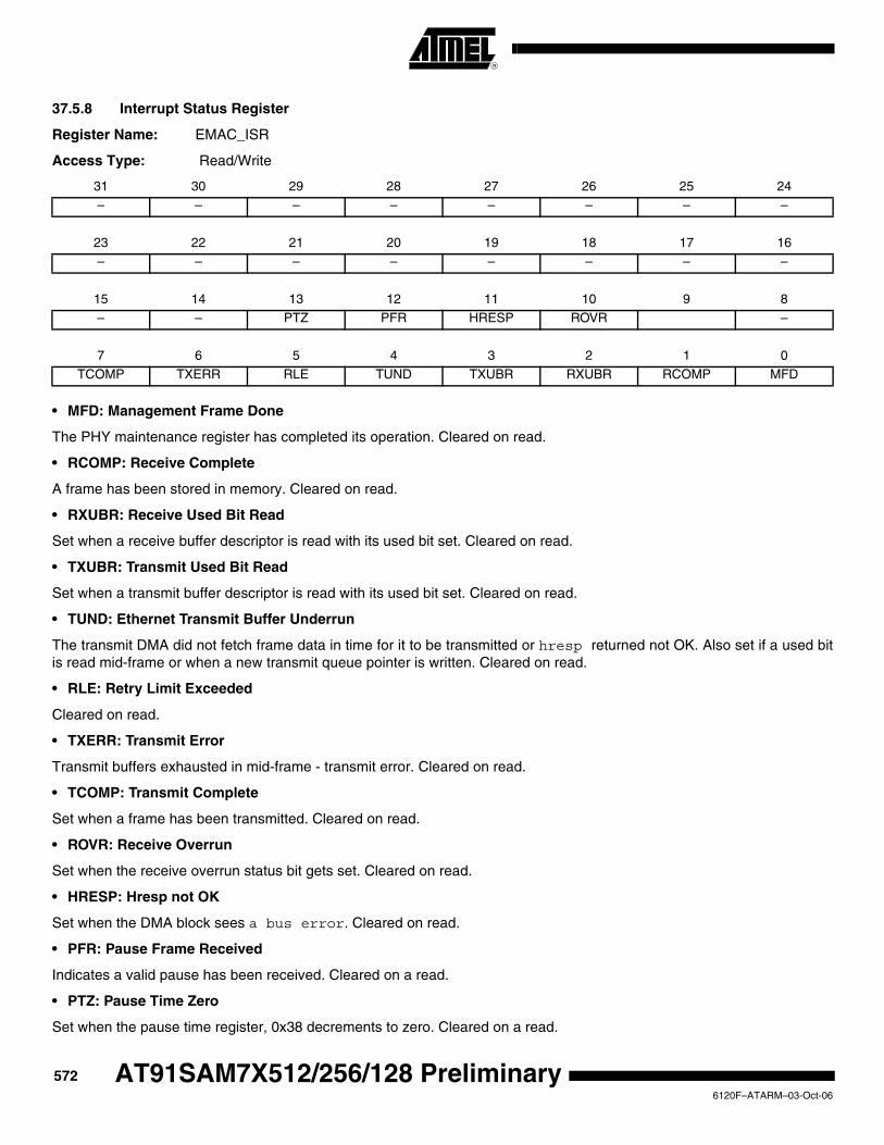
37.5.8 Interrupt Status Register
Register Name: EMAC_ISR
Access Type: Read/Write
• MFD: Management Frame Done
The PHY maintenance register has completed its operation. Cleared on read.
• RCOMP: Receive Complete
A frame has been stored in memory. Cleared on read.
• RXUBR: Receive Used Bit Read
Set when a receive buffer descriptor is read with its used bit set. Cleared on read.
• TXUBR: Transmit Used Bit Read
Set when a transmit buffer descriptor is read with its used bit set. Cleared on read.
• TUND: Ethernet Transmit Buffer Underrun
The transmit DMA did not fetch frame data in time for it to be transmitted or hresp returned not OK. Also set if a used bit is read mid-frame or when a new transmit queue pointer is written. Cleared on read.
• RLE: Retry Limit Exceeded
Cleared on read.
• TXERR: Transmit Error
Transmit buffers exhausted in mid-frame - transmit error. Cleared on read.
• TCOMP: Transmit Complete
Set when a frame has been transmitted. Cleared on read.
• ROVR: Receive Overrun
Set when the receive overrun status bit gets set. Cleared on read.
• HRESP: Hresp not OK
Set when the DMA block sees a bus error. Cleared on read.
• PFR: Pause Frame Received
Indicates a valid pause has been received. Cleared on a read.
• PTZ: Pause Time Zero
Set when the pause time register, 0x38 decrements to zero. Cleared on a read.
31 30 29 28 27 26 25 24– – – – – – – –
23 22 21 20 19 18 17 16
– – – – – – – –
15 14 13 12 11 10 9 8
– – PTZ PFR HRESP ROVR –
7 6 5 4 3 2 1 0
TCOMP TXERR RLE TUND TXUBR RXUBR RCOMP MFD
5726120F–ATARM–03-Oct-06
AT91SAM7X512/256/128 Preliminary

AT91SAM7X512/256/128 Preliminary
37.5.9 Interrupt Enable Register
Register Name: EMAC_IER
Access Type: Write-only
• MFD: Management Frame sent
Enable management done interrupt.
• RCOMP: Receive Complete
Enable receive complete interrupt.
• RXUBR: Receive Used Bit Read
Enable receive used bit read interrupt.
• TXUBR: Transmit Used Bit Read
Enable transmit used bit read interrupt.
• TUND: Ethernet Transmit Buffer Underrun
Enable transmit underrun interrupt.
• RLE: Retry Limit Exceeded
Enable retry limit exceeded interrupt.
• TXERR
Enable transmit buffers exhausted in mid-frame interrupt.
• TCOMP: Transmit Complete
Enable transmit complete interrupt.
• ROVR: Receive Overrun
Enable receive overrun interrupt.
• HRESP: Hresp not OK
Enable Hresp not OK interrupt.
• PFR: Pause Frame Received
Enable pause frame received interrupt.
• PTZ: Pause Time Zero
Enable pause time zero interrupt.
31 30 29 28 27 26 25 24– – – – – – – –
23 22 21 20 19 18 17 16
– – – – – – – –
15 14 13 12 11 10 9 8
– – PTZ PFR HRESP ROVR –
7 6 5 4 3 2 1 0
TCOMP TXERR RLE TUND TXUBR RXUBR RCOMP MFD
5736120F–ATARM–03-Oct-06

37.5.10 Interrupt Disable Register
Register Name: EMAC_IDR
Access Type: Write-only
• MFD: Management Frame sent
Disable management done interrupt.
• RCOMP: Receive Complete
Disable receive complete interrupt.
• RXUBR: Receive Used Bit Read
Disable receive used bit read interrupt.
• TXUBR: Transmit Used Bit Read
Disable transmit used bit read interrupt.
• TUND: Ethernet Transmit Buffer Underrun
Disable transmit underrun interrupt.
• RLE: Retry Limit Exceeded
Disable retry limit exceeded interrupt.
• TXERR
Disable transmit buffers exhausted in mid-frame interrupt.
• TCOMP: Transmit Complete
Disable transmit complete interrupt.
• ROVR: Receive Overrun
Disable receive overrun interrupt.
• HRESP: Hresp not OK
Disable Hresp not OK interrupt.
• PFR: Pause Frame Received
Disable pause frame received interrupt.
• PTZ: Pause Time Zero
Disable pause time zero interrupt.
31 30 29 28 27 26 25 24– – – – – – – –
23 22 21 20 19 18 17 16
– – – – – – – –
15 14 13 12 11 10 9 8
– – PTZ PFR HRESP ROVR –
7 6 5 4 3 2 1 0
TCOMP TXERR RLE TUND TXUBR RXUBR RCOMP MFD
5746120F–ATARM–03-Oct-06
AT91SAM7X512/256/128 Preliminary

AT91SAM7X512/256/128 Preliminary
37.5.11 Interrupt Mask Register
Register Name: EMAC_IMR
Access Type: Read-only
• MFD: Management Frame sent
Management done interrupt masked.
• RCOMP: Receive Complete
Receive complete interrupt masked.
• RXUBR: Receive Used Bit Read
Receive used bit read interrupt masked.
• TXUBR: Transmit Used Bit Read
Transmit used bit read interrupt masked.
• TUND: Ethernet Transmit Buffer Underrun
Transmit underrun interrupt masked.
• RLE: Retry Limit Exceeded
Retry limit exceeded interrupt masked.
• TXERR
Transmit buffers exhausted in mid-frame interrupt masked.
• TCOMP: Transmit Complete
Transmit complete interrupt masked.
• ROVR: Receive Overrun
Receive overrun interrupt masked.
• HRESP: Hresp not OK
Hresp not OK interrupt masked.
• PFR: Pause Frame Received
Pause frame received interrupt masked.
• PTZ: Pause Time Zero
Pause time zero interrupt masked.
31 30 29 28 27 26 25 24– – – – – – – –
23 22 21 20 19 18 17 16
– – – – – – – –
15 14 13 12 11 10 9 8
– – PTZ PFR HRESP ROVR –
7 6 5 4 3 2 1 0
TCOMP TXERR RLE TUND TXUBR RXUBR RCOMP MFD
5756120F–ATARM–03-Oct-06

37.5.12 PHY Maintenance Register
Register Name: EMAC_MAN
Access Type: Read/Write
• DATA
For a write operation this is written with the data to be written to the PHY.
After a read operation this contains the data read from the PHY.
• CODE:
Must be written to 10. Reads as written.
• REGA: Register Address
Specifies the register in the PHY to access.
• PHYA: PHY Address
• RW: Read/Write
10 is read; 01 is write. Any other value is an invalid PHY management frame
• SOF: Start of frame
Must be written 01 for a valid frame.
31 30 29 28 27 26 25 24SOF RW PHYA
23 22 21 20 19 18 17 16
PHYA REGA CODE
15 14 13 12 11 10 9 8
DATA
7 6 5 4 3 2 1 0
DATA
5766120F–ATARM–03-Oct-06
AT91SAM7X512/256/128 Preliminary

AT91SAM7X512/256/128 Preliminary
37.5.13 Pause Time Register
Register Name: EMAC_PTR
Access Type: Read/Write
• PTIME: Pause Time
Stores the current value of the pause time register which is decremented every 512 bit times.
31 30 29 28 27 26 25 24– – – – – – – –
23 22 21 20 19 18 17 16
– – – – – – – –
15 14 13 12 11 10 9 8
PTIME
7 6 5 4 3 2 1 0
PTIME
5776120F–ATARM–03-Oct-06
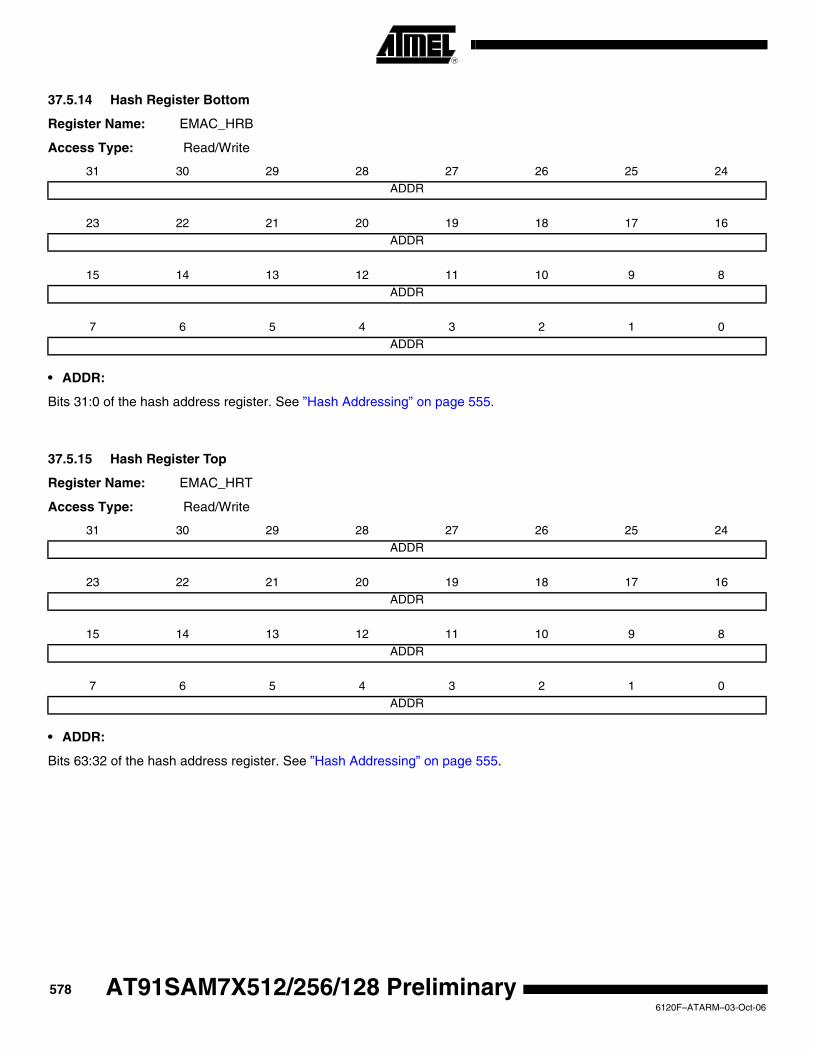
37.5.14 Hash Register Bottom
Register Name: EMAC_HRB
Access Type: Read/Write
• ADDR:
Bits 31:0 of the hash address register. See ”Hash Addressing” on page 555.
37.5.15 Hash Register Top
Register Name: EMAC_HRT
Access Type: Read/Write
• ADDR:
Bits 63:32 of the hash address register. See ”Hash Addressing” on page 555.
31 30 29 28 27 26 25 24ADDR
23 22 21 20 19 18 17 16
ADDR
15 14 13 12 11 10 9 8
ADDR
7 6 5 4 3 2 1 0
ADDR
31 30 29 28 27 26 25 24
ADDR
23 22 21 20 19 18 17 16
ADDR
15 14 13 12 11 10 9 8
ADDR
7 6 5 4 3 2 1 0
ADDR
5786120F–ATARM–03-Oct-06
AT91SAM7X512/256/128 Preliminary

AT91SAM7X512/256/128 Preliminary
37.5.16 Specific Address 1 Bottom Register
Register Name: EMAC_SA1B
Access Type: Read/Write
• ADDR
Least significant bits of the destination address. Bit zero indicates whether the address is multicast or unicast and corre-sponds to the least significant bit of the first byte received.
37.5.17 Specific Address 1 Top Register
Register Name: EMAC_SA1T
Access Type: Read/Write
• ADDR
The most significant bits of the destination address, that is bits 47 to 32.
31 30 29 28 27 26 25 24ADDR
23 22 21 20 19 18 17 16
ADDR
15 14 13 12 11 10 9 8
ADDR
7 6 5 4 3 2 1 0
ADDR
31 30 29 28 27 26 25 24
– – – – – – – –
23 22 21 20 19 18 17 16
– – – – – – – –
15 14 13 12 11 10 9 8
ADDR
7 6 5 4 3 2 1 0
ADDR
5796120F–ATARM–03-Oct-06

37.5.18 Specific Address 2 Bottom Register
Register Name: EMAC_SA2B
Access Type: Read/Write
• ADDR
Least significant bits of the destination address. Bit zero indicates whether the address is multicast or unicast and corre-sponds to the least significant bit of the first byte received.
37.5.19 Specific Address 2 Top Register
Register Name: EMAC_SA2T
Access Type: Read/Write
• ADDR
The most significant bits of the destination address, that is bits 47 to 32.
31 30 29 28 27 26 25 24ADDR
23 22 21 20 19 18 17 16
ADDR
15 14 13 12 11 10 9 8
ADDR
7 6 5 4 3 2 1 0
ADDR
31 30 29 28 27 26 25 24
– – – – – – – –
23 22 21 20 19 18 17 16
– – – – – – – –
15 14 13 12 11 10 9 8
ADDR
7 6 5 4 3 2 1 0
ADDR
5806120F–ATARM–03-Oct-06
AT91SAM7X512/256/128 Preliminary

AT91SAM7X512/256/128 Preliminary
37.5.20 Specific Address 3 Bottom Register
Register Name: EMAC_SA3B
Access Type: Read/Write
• ADDR
Least significant bits of the destination address. Bit zero indicates whether the address is multicast or unicast and corre-sponds to the least significant bit of the first byte received.
37.5.21 Specific Address 3 Top Register
Register Name: EMAC_SA3T
Access Type: Read/Write
• ADDR
The most significant bits of the destination address, that is bits 47 to 32.
31 30 29 28 27 26 25 24ADDR
23 22 21 20 19 18 17 16
ADDR
15 14 13 12 11 10 9 8
ADDR
7 6 5 4 3 2 1 0
ADDR
31 30 29 28 27 26 25 24
– – – – – – – –
23 22 21 20 19 18 17 16
– – – – – – – –
15 14 13 12 11 10 9 8
ADDR
7 6 5 4 3 2 1 0
ADDR
5816120F–ATARM–03-Oct-06

37.5.22 Specific Address 4 Bottom Register
Register Name: EMAC_SA4B
Access Type: Read/Write
• ADDR
Least significant bits of the destination address. Bit zero indicates whether the address is multicast or unicast and corre-sponds to the least significant bit of the first byte received.
37.5.23 Specific Address 4 Top Register
Register Name: EMAC_SA4T
Access Type: Read/Write
• ADDR
The most significant bits of the destination address, that is bits 47 to 32.
31 30 29 28 27 26 25 24ADDR
23 22 21 20 19 18 17 16
ADDR
15 14 13 12 11 10 9 8
ADDR
7 6 5 4 3 2 1 0
ADDR
31 30 29 28 27 26 25 24
– – – – – – – –
23 22 21 20 19 18 17 16
– – – – – – – –
15 14 13 12 11 10 9 8
ADDR
7 6 5 4 3 2 1 0
ADDR
5826120F–ATARM–03-Oct-06
AT91SAM7X512/256/128 Preliminary

AT91SAM7X512/256/128 Preliminary
37.5.24 Type ID Checking Register
Register Name: EMAC_TID
Access Type: Read/Write
• TID: Type ID Checking
For use in comparisons with received frames TypeID/Length field.
37.5.25 User Input/Output Register
Register Name: EMAC_USRIO
Access Type: Read/Write
• RMII
When set, this bit enables the RMII operation mode. When reset, it selects the MII mode.
• CLKEN
When set, this bit enables the transceiver input clock.
Setting this bit to 0 reduces power consumption when the treasurer is not used.
31 30 29 28 27 26 25 24– – – – – – – –
23 22 21 20 19 18 17 16
– – – – – – – –
15 14 13 12 11 10 9 8
TID
7 6 5 4 3 2 1 0
TID
31 30 29 28 27 26 25 24
– – – – – – – –
23 22 21 20 19 18 17 16
– – – – – – – –
15 14 13 12 11 10 9 8
– – – – – – – –
7 6 5 4 3 2 1 0
– – – – – – CLKEN RMII
5836120F–ATARM–03-Oct-06

37.5.26 EMAC Statistic Registers
These registers reset to zero on a read and stick at all ones when they count to their maximum value. They should be read frequently enough to prevent loss of data. The receive statistics registers are only incremented when the receive enable bit is set in the network control register. To write to these registers, bit 7 must be set in the network control register. The statis-tics register block contains the following registers.
37.5.26.1 Pause Frames Received Register
Register Name: EMAC_PFR
Access Type: Read/Write
• FROK: Pause Frames Received OK
A 16-bit register counting the number of good pause frames received. A good frame has a length of 64 to 1518 (1536 if bit 8 set in network configuration register) and has no FCS, alignment or receive symbol errors.
37.5.26.2 Frames Transmitted OK Register
Register Name: EMAC_FTO
Access Type: Read/Write
• FTOK: Frames Transmitted OK
A 24-bit register counting the number of frames successfully transmitted, i.e., no underrun and not too many retries.
31 30 29 28 27 26 25 24
– – – – – – – –
23 22 21 20 19 18 17 16
– – – – – – – –
15 14 13 12 11 10 9 8
FROK
7 6 5 4 3 2 1 0
FROK
31 30 29 28 27 26 25 24
– – – – – – – –
23 22 21 20 19 18 17 16
FTOK
15 14 13 12 11 10 9 8
FTOK
7 6 5 4 3 2 1 0
FTOK
5846120F–ATARM–03-Oct-06
AT91SAM7X512/256/128 Preliminary

AT91SAM7X512/256/128 Preliminary
37.5.26.3 Single Collision Frames Register
Register Name: EMAC_SCF
Access Type: Read/Write
• SCF: Single Collision Frames
A 16-bit register counting the number of frames experiencing a single collision before being successfully transmitted, i.e., no underrun.
37.5.26.4 Multicollision Frames Register
Register Name: EMAC_MCF
Access Type: Read/Write
• MCF: Multicollision Frames
A 16-bit register counting the number of frames experiencing between two and fifteen collisions prior to being successfully transmitted, i.e., no underrun and not too many retries.
31 30 29 28 27 26 25 24– – – – – – – –
23 22 21 20 19 18 17 16
– – – – – – – –
15 14 13 12 11 10 9 8
SCF
7 6 5 4 3 2 1 0
SCF
31 30 29 28 27 26 25 24
– – – – – – – –
23 22 21 20 19 18 17 16
– – – – – – – –
15 14 13 12 11 10 9 8
MCF
7 6 5 4 3 2 1 0
MCF
5856120F–ATARM–03-Oct-06
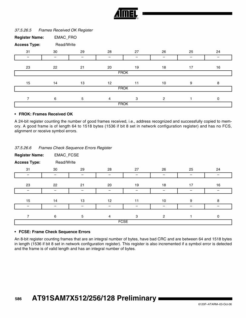
37.5.26.5 Frames Received OK Register
Register Name: EMAC_FRO
Access Type: Read/Write
• FROK: Frames Received OK
A 24-bit register counting the number of good frames received, i.e., address recognized and successfully copied to mem-ory. A good frame is of length 64 to 1518 bytes (1536 if bit 8 set in network configuration register) and has no FCS, alignment or receive symbol errors.
37.5.26.6 Frames Check Sequence Errors Register
Register Name: EMAC_FCSE
Access Type: Read/Write
• FCSE: Frame Check Sequence Errors
An 8-bit register counting frames that are an integral number of bytes, have bad CRC and are between 64 and 1518 bytes in length (1536 if bit 8 set in network configuration register). This register is also incremented if a symbol error is detected and the frame is of valid length and has an integral number of bytes.
31 30 29 28 27 26 25 24– – – – – – – –
23 22 21 20 19 18 17 16
FROK
15 14 13 12 11 10 9 8
FROK
7 6 5 4 3 2 1 0
FROK
31 30 29 28 27 26 25 24
– – – – – – – –
23 22 21 20 19 18 17 16
– – – – – – – –
15 14 13 12 11 10 9 8
– – – – – – – –
7 6 5 4 3 2 1 0
FCSE
5866120F–ATARM–03-Oct-06
AT91SAM7X512/256/128 Preliminary
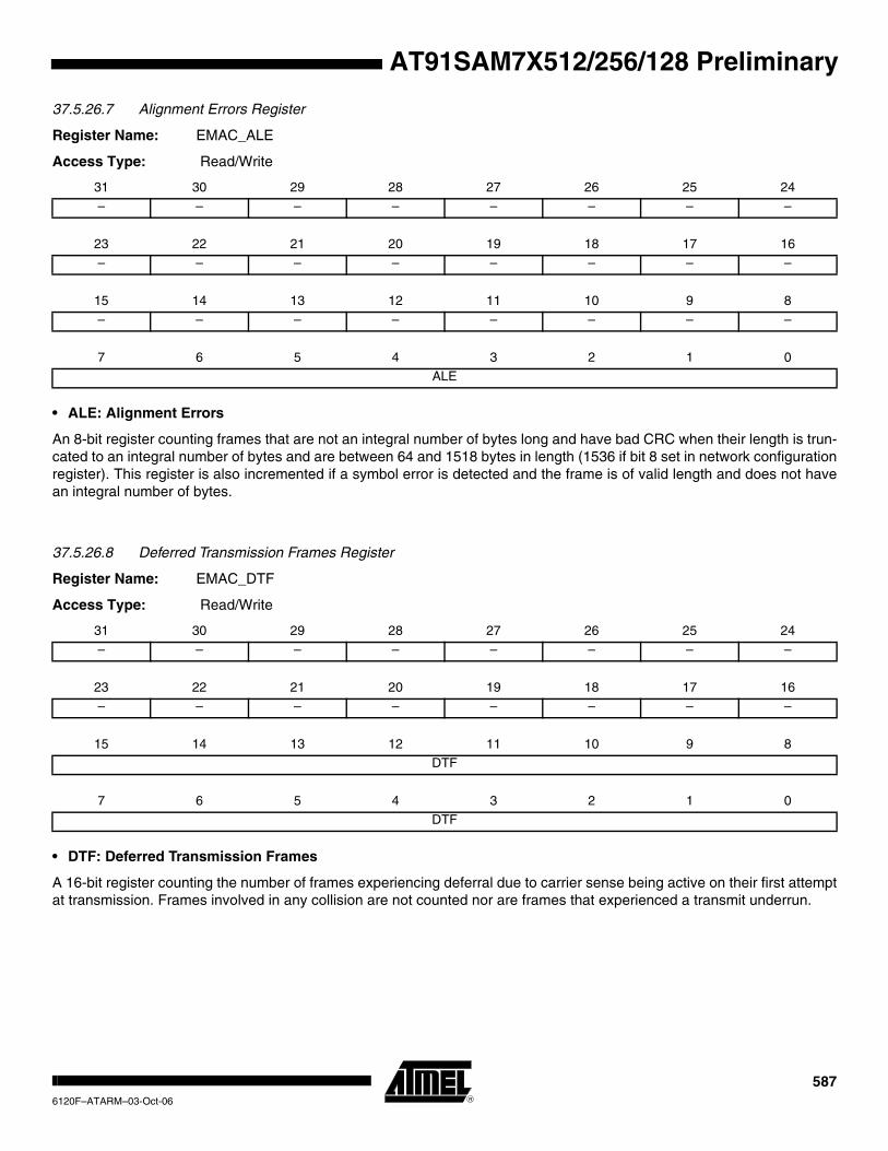
AT91SAM7X512/256/128 Preliminary
37.5.26.7 Alignment Errors Register
Register Name: EMAC_ALE
Access Type: Read/Write
• ALE: Alignment Errors
An 8-bit register counting frames that are not an integral number of bytes long and have bad CRC when their length is trun-cated to an integral number of bytes and are between 64 and 1518 bytes in length (1536 if bit 8 set in network configuration register). This register is also incremented if a symbol error is detected and the frame is of valid length and does not have an integral number of bytes.
37.5.26.8 Deferred Transmission Frames Register
Register Name: EMAC_DTF
Access Type: Read/Write
• DTF: Deferred Transmission Frames
A 16-bit register counting the number of frames experiencing deferral due to carrier sense being active on their first attempt at transmission. Frames involved in any collision are not counted nor are frames that experienced a transmit underrun.
31 30 29 28 27 26 25 24– – – – – – – –
23 22 21 20 19 18 17 16
– – – – – – – –
15 14 13 12 11 10 9 8
– – – – – – – –
7 6 5 4 3 2 1 0
ALE
31 30 29 28 27 26 25 24
– – – – – – – –
23 22 21 20 19 18 17 16
– – – – – – – –
15 14 13 12 11 10 9 8
DTF
7 6 5 4 3 2 1 0
DTF
5876120F–ATARM–03-Oct-06

37.5.26.9 Late Collisions Register
Register Name: EMAC_LCOL
Access Type: Read/Write
• LCOL: Late Collisions
An 8-bit register counting the number of frames that experience a collision after the slot time (512 bits) has expired. A late collision is counted twice; i.e., both as a collision and a late collision.
37.5.26.10 Excessive Collisions Register
Register Name: EMAC_EXCOL
Access Type: Read/Write
• EXCOL: Excessive Collisions
An 8-bit register counting the number of frames that failed to be transmitted because they experienced 16 collisions.
31 30 29 28 27 26 25 24– – – – – – – –
23 22 21 20 19 18 17 16
– – – – – – – –
15 14 13 12 11 10 9 8
– – – – – – – –
7 6 5 4 3 2 1 0
LCOL
31 30 29 28 27 26 25 24
– – – – – – – –
23 22 21 20 19 18 17 16
– – – – – – – –
15 14 13 12 11 10 9 8
– – – – – – – –
7 6 5 4 3 2 1 0
EXCOL
5886120F–ATARM–03-Oct-06
AT91SAM7X512/256/128 Preliminary

AT91SAM7X512/256/128 Preliminary
37.5.26.11 Transmit Underrun Errors Register
Register Name: EMAC_TUND
Access Type: Read/Write
• TUND: Transmit Underruns
An 8-bit register counting the number of frames not transmitted due to a transmit DMA underrun. If this register is incre-mented, then no other statistics register is incremented.
37.5.26.12 Carrier Sense Errors Register
Register Name: EMAC_CSE
Access Type: Read/Write
• CSE: Carrier Sense Errors
An 8-bit register counting the number of frames transmitted where carrier sense was not seen during transmission or where carrier sense was deasserted after being asserted in a transmit frame without collision (no underrun). Only incremented in half-duplex mode. The only effect of a carrier sense error is to increment this register. The behavior of the other statistics registers is unaffected by the detection of a carrier sense error.
31 30 29 28 27 26 25 24– – – – – – – –
23 22 21 20 19 18 17 16
– – – – – – – –
15 14 13 12 11 10 9 8
– – – – – – – –
7 6 5 4 3 2 1 0
TUND
31 30 29 28 27 26 25 24
– – – – – – – –
23 22 21 20 19 18 17 16
– – – – – – – –
15 14 13 12 11 10 9 8
– – – – – – – –
7 6 5 4 3 2 1 0
CSE
5896120F–ATARM–03-Oct-06
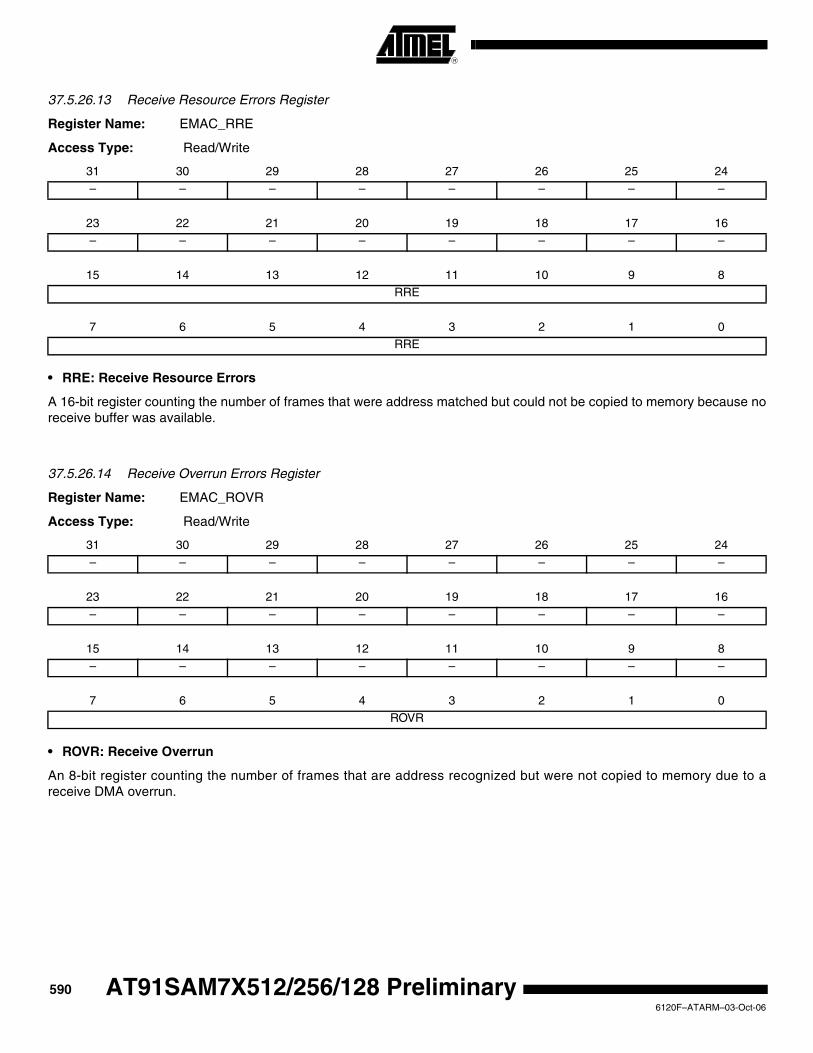
37.5.26.13 Receive Resource Errors Register
Register Name: EMAC_RRE
Access Type: Read/Write
• RRE: Receive Resource Errors
A 16-bit register counting the number of frames that were address matched but could not be copied to memory because no receive buffer was available.
37.5.26.14 Receive Overrun Errors Register
Register Name: EMAC_ROVR
Access Type: Read/Write
• ROVR: Receive Overrun
An 8-bit register counting the number of frames that are address recognized but were not copied to memory due to a receive DMA overrun.
31 30 29 28 27 26 25 24– – – – – – – –
23 22 21 20 19 18 17 16
– – – – – – – –
15 14 13 12 11 10 9 8
RRE
7 6 5 4 3 2 1 0
RRE
31 30 29 28 27 26 25 24
– – – – – – – –
23 22 21 20 19 18 17 16
– – – – – – – –
15 14 13 12 11 10 9 8
– – – – – – – –
7 6 5 4 3 2 1 0
ROVR
5906120F–ATARM–03-Oct-06
AT91SAM7X512/256/128 Preliminary
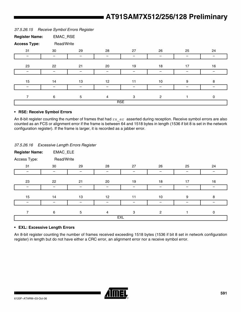
AT91SAM7X512/256/128 Preliminary
37.5.26.15 Receive Symbol Errors Register
Register Name: EMAC_RSE
Access Type: Read/Write
• RSE: Receive Symbol Errors
An 8-bit register counting the number of frames that had rx_er asserted during reception. Receive symbol errors are also counted as an FCS or alignment error if the frame is between 64 and 1518 bytes in length (1536 if bit 8 is set in the network configuration register). If the frame is larger, it is recorded as a jabber error.
37.5.26.16 Excessive Length Errors Register
Register Name: EMAC_ELE
Access Type: Read/Write
• EXL: Excessive Length Errors
An 8-bit register counting the number of frames received exceeding 1518 bytes (1536 if bit 8 set in network configuration register) in length but do not have either a CRC error, an alignment error nor a receive symbol error.
31 30 29 28 27 26 25 24– – – – – – – –
23 22 21 20 19 18 17 16
– – – – – – – –
15 14 13 12 11 10 9 8
– – – – – – – –
7 6 5 4 3 2 1 0
RSE
31 30 29 28 27 26 25 24
– – – – – – – –
23 22 21 20 19 18 17 16
– – – – – – – –
15 14 13 12 11 10 9 8
– – – – – – – –
7 6 5 4 3 2 1 0
EXL
5916120F–ATARM–03-Oct-06

37.5.26.17 Receive Jabbers Register
Register Name: EMAC_RJA
Access Type: Read/Write
• RJB: Receive Jabbers
An 8-bit register counting the number of frames received exceeding 1518 bytes (1536 if bit 8 set in network configuration register) in length and have either a CRC error, an alignment error or a receive symbol error.
37.5.26.18 Undersize Frames Register
Register Name: EMAC_USF
Access Type: Read/Write
• USF: Undersize Frames
An 8-bit register counting the number of frames received less than 64 bytes in length but do not have either a CRC error, an alignment error or a receive symbol error.
31 30 29 28 27 26 25 24– – – – – – – –
23 22 21 20 19 18 17 16
– – – – – – – –
15 14 13 12 11 10 9 8
– – – – – – – –
7 6 5 4 3 2 1 0
RJB
31 30 29 28 27 26 25 24
– – – – – – – –
23 22 21 20 19 18 17 16
– – – – – – – –
15 14 13 12 11 10 9 8
– – – – – – – –
7 6 5 4 3 2 1 0
USF
5926120F–ATARM–03-Oct-06
AT91SAM7X512/256/128 Preliminary

AT91SAM7X512/256/128 Preliminary
37.5.26.19 SQE Test Errors Register
Register Name: EMAC_STE
Access Type: Read/Write
• SQER: SQE Test Errors
An 8-bit register counting the number of frames where ECOL was not asserted within 96 bit times (an interframe gap) of tx_en being deasserted in half duplex mode.
37.5.26.20 Received Length Field Mismatch Register
Register Name: EMAC_RLE
Access Type: Read/Write
• RLFM: Receive Length Field Mismatch
An 8-bit register counting the number of frames received that have a measured length shorter than that extracted from its length field. Checking is enabled through bit 16 of the network configuration register. Frames containing a type ID in bytes 13 and 14 (i.e., length/type ID ≥ 0x0600) are not counted as length field errors, neither are excessive length frames.
31 30 29 28 27 26 25 24– – – – – – – –
23 22 21 20 19 18 17 16
– – – – – – – –
15 14 13 12 11 10 9 8
– – – – – – – –
7 6 5 4 3 2 1 0
SQER
31 30 29 28 27 26 25 24
– – – – – – – –
23 22 21 20 19 18 17 16
– – – – – – – –
15 14 13 12 11 10 9 8
– – – – – – – –
7 6 5 4 3 2 1 0
RLFM
5936120F–ATARM–03-Oct-06

5946120F–ATARM–03-Oct-06
AT91SAM7X512/256/128 Preliminary
AT91SAM7X512/256/128 Preliminary
38. AT91SAM7X Electrical Characteristics
38.1 Absolute Maximum Ratings
Table 38-1. Absolute Maximum Ratings*
Operating Temperature (Industrial).........-40°C to + 85°C *NOTICE: Stresses beyond those listed under “Absolute Maxi-mum Ratings” may cause permanent damage to the device. This is a stress rating only and func-tional operation of the device at these or other con-ditions beyond those indicated in the operational sections of this specification is not implied. Expo-sure to absolute maximum rating conditions for extended periods may affect device reliability.
Storage Temperature............................-60°C to + 150°C
Voltage on Input Pins with Respect to Ground...........................-0.3V to + 5.5V
Maximum Operating Voltage (VDDCORE, and VDDPLL)........................................2.0V
Maximum Operating Voltage (VDDIO, VDDIN and VDDFLASH)...........................4.0V
Total DC Output Current on all I/O lines 100-lead LQFP package........................................200 mA
5956120F–ATARM–03-Oct-06

38.2 DC CharacteristicsThe following characteristics are applicable to the operating temperature range: TA = -40°C to 85°C, unless otherwise spec-ified and are certified for a junction temperature up to TJ = 100°C.
Note that even during startup, VVDDFLASH must always be superior or equal to VVDDCORE.
Table 38-2. DC Characteristics
Symbol Parameter Conditions Min Typ Max Units
VVDDCORE DC Supply Core 1.65 1.95 V
VVDDPLL DC Supply PLL 1.65 1.95 V
VVDDIO DC Supply I/Os 3.0 3.6 V
VVDDFLASH DC Supply Flash 3.0 3.6 V
VIL Input Low-level Voltage VVDDIO from 3.0V to 3.6V -0.3 0.8 V
VIH Input High-level Voltage VVDDIO from 3.0V to 3.6V 2.0 5.5 V
VOL Output Low-level Voltage IO max, VVDDIO from 3.0V to 3.6V 0.4 V
VOH Output High-level Voltage IO max, VVDDIO from 3.0V to 3.6V VDDIO - 0.4 V
ILEAK Input Leakage Current
PA0-PA3, Pull-up resistors disabled (Typ: TA = 25°C, Max: TA = 85°C)
40 400 nA
Other PIOs and NRST, Pull-up resistors disabled (Typ: TA = 25°C, Max: TA = 85°C)
20 200 nA
IPULLUP Input Pull-up Current
PB27-PB30, VVDDIO from 3.0V to 3.6V, PAx connected to ground
10 20.6 60 µA
Other PIOs and NRST, VVDDIO from 3.0V to 3.6V, PAx connected to ground
143 321 600 µA
IPULLDOWNInput Pull-down Current,(TST, ERASE, JTAGSEL)
VVDDIO from 3.0V to 3.6V,Pins connected to VVDDIO
135 295 550 µA
CIN Input Capacitance 100 LQFP Package 13.9 pF
ISCStatic Current (AT91SAM7X512/256/128)
On VVDDCORE = 1.85V,
MCK = 500HzTA = 25°C 12 60
µAAll inputs driven at 1 (including TMS, TDI, TCK, NRST) Flash in standby mode All peripherals off
TA = 85°C 100 400
IO Output Current
PA0-PA3, VVDDIO from 3.0V to 3.6V 16 mA
PB27-PB30 and NRST, VVDDIO from 3.0V to 3.6V 2 mA
Other PIOs, VVDDIO from 3.0V to 3.6V 8 mA
TSLOPE Supply Core Slope 6 V/ms
5966120F–ATARM–03-Oct-06
AT91SAM7X512/256/128 Preliminary
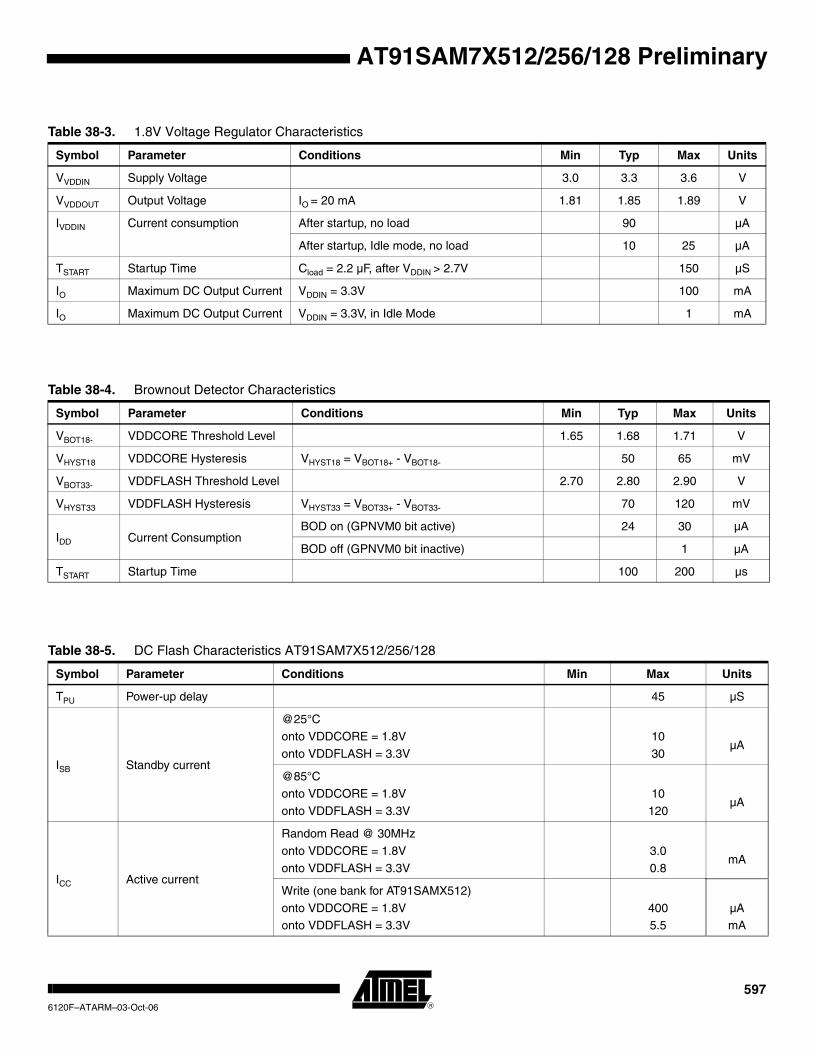
AT91SAM7X512/256/128 Preliminary
Table 38-3. 1.8V Voltage Regulator Characteristics
Symbol Parameter Conditions Min Typ Max Units
VVDDIN Supply Voltage 3.0 3.3 3.6 V
VVDDOUT Output Voltage IO = 20 mA 1.81 1.85 1.89 V
IVDDIN Current consumption After startup, no load 90 µA
After startup, Idle mode, no load 10 25 µA
TSTART Startup Time Cload = 2.2 µF, after VDDIN > 2.7V 150 µS
IO Maximum DC Output Current VDDIN = 3.3V 100 mA
IO Maximum DC Output Current VDDIN = 3.3V, in Idle Mode 1 mA
Table 38-4. Brownout Detector Characteristics
Symbol Parameter Conditions Min Typ Max Units
VBOT18- VDDCORE Threshold Level 1.65 1.68 1.71 V
VHYST18 VDDCORE Hysteresis VHYST18 = VBOT18+ - VBOT18- 50 65 mV
VBOT33- VDDFLASH Threshold Level 2.70 2.80 2.90 V
VHYST33 VDDFLASH Hysteresis VHYST33 = VBOT33+ - VBOT33- 70 120 mV
IDD Current ConsumptionBOD on (GPNVM0 bit active) 24 30 µA
BOD off (GPNVM0 bit inactive) 1 µA
TSTART Startup Time 100 200 µs
Table 38-5. DC Flash Characteristics AT91SAM7X512/256/128
Symbol Parameter Conditions Min Max Units
TPU Power-up delay 45 µS
ISB Standby current
@25°Conto VDDCORE = 1.8V
onto VDDFLASH = 3.3V
10
30µA
@85°C
onto VDDCORE = 1.8V
onto VDDFLASH = 3.3V
10
120µA
ICC Active current
Random Read @ 30MHz
onto VDDCORE = 1.8V
onto VDDFLASH = 3.3V
3.0
0.8mA
Write (one bank for AT91SAMX512)
onto VDDCORE = 1.8Vonto VDDFLASH = 3.3V
4005.5
µAmA
5976120F–ATARM–03-Oct-06

38.3 Power Consumption• Typical power consumption of PLLs, Slow Clock and Main Oscillator.
• Power consumption of power supply in two different modes: Active and ultra Low-power.
• Power consumption by peripheral: calculated as the difference in current measurement after having enabled then disabled the corresponding clock.
38.3.1 Power Consumption Versus ModesThe values in Table 38-6 and Table 38-7 on page 599 are measured values of the power con-sumption with operating conditions as follows:
• VDDIO = VDDIN = VDDFLASH= 3.3V
• VDDCORE = VDDPLL = 1.85V
• TA = 25°C
• There is no consumption on the I/Os of the device
Figure 38-1. Measure Schematics:
1.8V
VDDIN
VoltageRegulator
VDDOUT
VDDCORE
VDDPLL
3.3V
VDDIO
VDDFLASH
AMP1
AMP2
5986120F–ATARM–03-Oct-06
AT91SAM7X512/256/128 Preliminary

AT91SAM7X512/256/128 Preliminary
These figures represent the power consumption typically measured on the power supplies..
38.3.2 Peripheral Power Consumption in Active Mode
Note: 1. Note: VDDCORE = 1.85V, TA = 25°C
Table 38-6. Power Consumption for Different Modes
Mode Conditions Consumption Unit
Active(AT91SAM7X512/256/128)
Voltage regulator is on.Brown Out Detector is activated.
Flash is read.
ARM Core clock is 50MHz.
Analog-to-Digital Converter activated.All peripheral clocks activated.
USB transceiver enabled.
onto AMP1onto AMP2
5049
mA
Ultra low power
Voltage regulator is in Low-power mode.Brown Out Detector is de-activated.
Flash is in standby mode.
ARM Core in idle mode.MCK @ 500Hz.
Analog-to-Digital Converter de-activated.
All peripheral clocks de-activated.USB transceiver disabled.
DDM and DDP pins connected to ground.
onto AMP1onto AMP2
2612
µA
Table 38-7. Power Consumption on VDDCORE(1)
Peripheral Consumption (Typ) Unit
PIO Controller 12
µA/MHz
USART 28
UDP 20
PWM 16
TWI 5
SPI 16
SSC 32
Timer Counter Channels 6
CAN 75
ARM7TDMI 160
EMAC 120
System Peripherals (AT91SAM7X512/256/128)
200
5996120F–ATARM–03-Oct-06
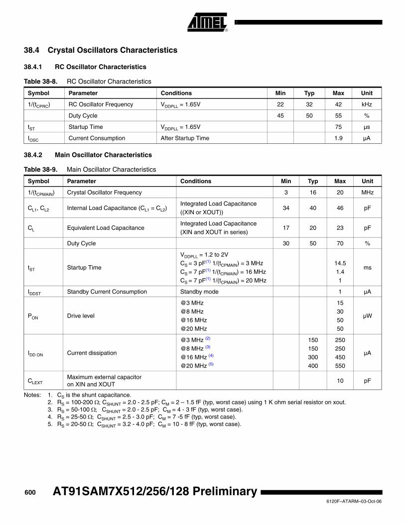
38.4 Crystal Oscillators Characteristics
38.4.1 RC Oscillator Characteristics
38.4.2 Main Oscillator Characteristics
Notes: 1. CS is the shunt capacitance.2. RS = 100-200 Ω; CSHUNT = 2.0 - 2.5 pF; CM = 2 – 1.5 fF (typ, worst case) using 1 K ohm serial resistor on xout.3. RS = 50-100 Ω; CSHUNT = 2.0 - 2.5 pF; CM = 4 - 3 fF (typ, worst case).4. RS = 25-50 Ω; CSHUNT = 2.5 - 3.0 pF; CM = 7 -5 fF (typ, worst case).5. RS = 20-50 Ω; CSHUNT = 3.2 - 4.0 pF; CM = 10 - 8 fF (typ, worst case).
Table 38-8. RC Oscillator Characteristics
Symbol Parameter Conditions Min Typ Max Unit
1/(tCPRC) RC Oscillator Frequency VDDPLL = 1.65V 22 32 42 kHz
Duty Cycle 45 50 55 %
tST Startup Time VDDPLL = 1.65V 75 µs
IOSC Current Consumption After Startup Time 1.9 µA
Table 38-9. Main Oscillator Characteristics
Symbol Parameter Conditions Min Typ Max Unit
1/(tCPMAIN) Crystal Oscillator Frequency 3 16 20 MHz
CL1, CL2 Internal Load Capacitance (CL1 = CL2)Integrated Load Capacitance
((XIN or XOUT))34 40 46 pF
CL Equivalent Load CapacitanceIntegrated Load Capacitance
(XIN and XOUT in series)17 20 23 pF
Duty Cycle 30 50 70 %
tST Startup Time
VDDPLL = 1.2 to 2VCS = 3 pF(1) 1/(tCPMAIN) = 3 MHz
CS = 7 pF(1) 1/(tCPMAIN) = 16 MHz
CS = 7 pF(1) 1/(tCPMAIN) = 20 MHz
14.5
1.4
1
ms
IDDST Standby Current Consumption Standby mode 1 µA
PON Drive level
@3 MHz
@8 MHz
@16 MHz@20 MHz
15
30
5050
µW
IDD ON Current dissipation
@3 MHz (2)
@8 MHz (3)
@16 MHz (4)
@20 MHz (5)
150150
300
400
250250
450
550
µA
CLEXTMaximum external capacitor on XIN and XOUT
10 pF
6006120F–ATARM–03-Oct-06
AT91SAM7X512/256/128 Preliminary
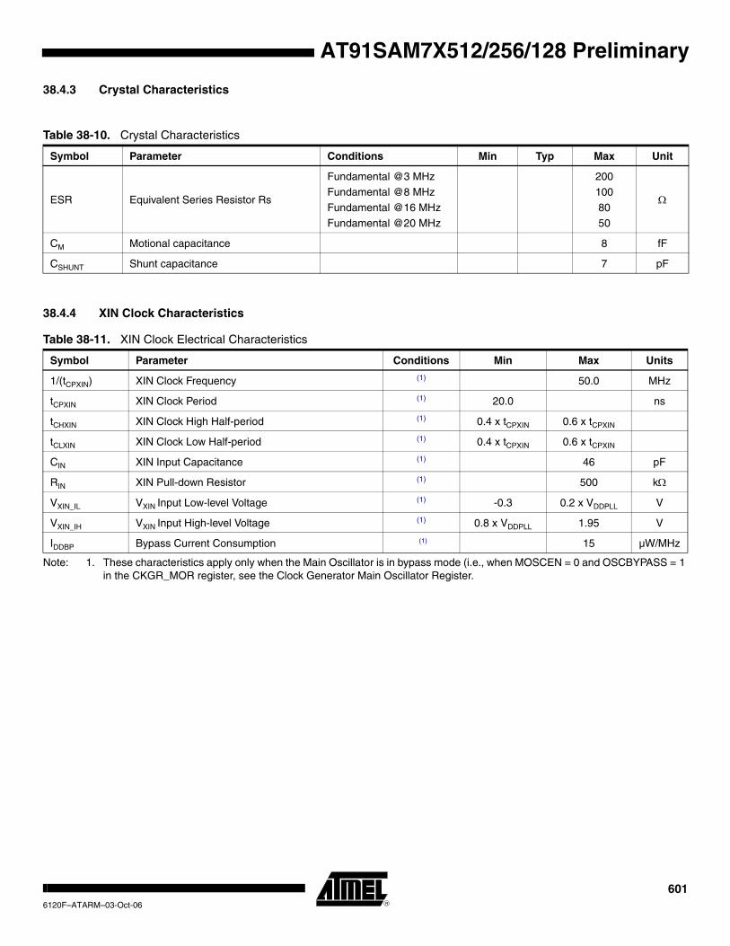
AT91SAM7X512/256/128 Preliminary
38.4.3 Crystal Characteristics
38.4.4 XIN Clock Characteristics
Note: 1. These characteristics apply only when the Main Oscillator is in bypass mode (i.e., when MOSCEN = 0 and OSCBYPASS = 1 in the CKGR_MOR register, see the Clock Generator Main Oscillator Register.
Table 38-10. Crystal Characteristics
Symbol Parameter Conditions Min Typ Max Unit
ESR Equivalent Series Resistor Rs
Fundamental @3 MHz
Fundamental @8 MHz
Fundamental @16 MHz
Fundamental @20 MHz
200
100
80
50
Ω
CM Motional capacitance 8 fF
CSHUNT Shunt capacitance 7 pF
Table 38-11. XIN Clock Electrical Characteristics
Symbol Parameter Conditions Min Max Units
1/(tCPXIN) XIN Clock Frequency (1) 50.0 MHz
tCPXIN XIN Clock Period (1) 20.0 ns
tCHXIN XIN Clock High Half-period (1) 0.4 x tCPXIN 0.6 x tCPXIN
tCLXIN XIN Clock Low Half-period (1) 0.4 x tCPXIN 0.6 x tCPXIN
CIN XIN Input Capacitance (1) 46 pF
RIN XIN Pull-down Resistor (1) 500 kΩ
VXIN_IL VXIN Input Low-level Voltage (1) -0.3 0.2 x VDDPLL V
VXIN_IH VXIN Input High-level Voltage (1) 0.8 x VDDPLL 1.95 V
IDDBP Bypass Current Consumption (1) 15 µW/MHz
6016120F–ATARM–03-Oct-06
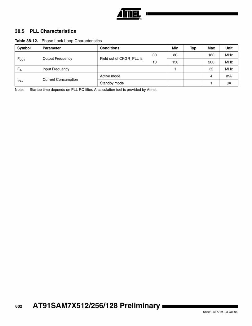
38.5 PLL Characteristics
Note: Startup time depends on PLL RC filter. A calculation tool is provided by Atmel.
Table 38-12. Phase Lock Loop Characteristics
Symbol Parameter Conditions Min Typ Max Unit
FOUT Output Frequency Field out of CKGR_PLL is:00 80 160 MHz
10 150 200 MHz
FIN Input Frequency 1 32 MHz
IPLL Current ConsumptionActive mode 4 mA
Standby mode 1 µA
6026120F–ATARM–03-Oct-06
AT91SAM7X512/256/128 Preliminary

AT91SAM7X512/256/128 Preliminary
38.6 USB Transceiver Characteristics
38.6.1 Electrical Characteristics
38.6.2 Switching Characteristics
Table 38-13. Electrical Parameters
Symbol Parameter Conditions Min Typ Max Unit
Input Levels
VIL Low Level 0.8 V
VIH High Level 2.0 V
VDI Differential Input Sensitivity |(D+) - (D-)| 0.2 V
VCM
Differential Input Common Mode Range
0.8 2.5 V
CIN Transceiver capacitance Capacitance to ground on each line 9.18 pF
I Hi-Z State Data Line Leakage 0V < VIN < 3.3V -10 +10 µA
REXT
Recommended External USB Series Resistor
In series with each USB pin with ±5% 27 Ω
Output Levels
VOL Low Level OutputMeasured with RL of 1.425 kOhm tied to 3.6V
0.0 0.3 V
VOH High Level OutputMeasured with RL of 14.25 kOhm tied to GND
2.8 3.6 V
VCRS
Output Signal Crossover Voltage
Measure conditions described in Figure 38-2
1.3 2.0 V
Consumption
IVDDIO Current Consumption Transceiver enabled in input mode DDP=1 and DDM=0
105 200 µA
IVDDCORE Current Consumption 80 150 µA
Table 38-14. In Full Speed
Symbol Parameter Conditions Min Typ Max Unit
tFR Transition Rise Time CLOAD = 50 pF 4 20 ns
tFE Transition Fall Time CLOAD = 50 pF 4 20 ns
tFRFM Rise/Fall time Matching 90 111.11 %
6036120F–ATARM–03-Oct-06

Figure 38-2. USB Data Signal Rise and Fall Times
10% 10%
90%VCRS
tR tFDifferentialData Lines
Rise Time Fall Time
Fosc = 6MHz/750kHzREXT=27 ohms
CloadBuffer
(b)
(a)
6046120F–ATARM–03-Oct-06
AT91SAM7X512/256/128 Preliminary

AT91SAM7X512/256/128 Preliminary
38.7 ADC Characteristics
Notes: 1. Corresponds to 13 clock cycles at 5 MHz: 3 clock cycles for track and hold acquisition time and 10 clock cycles for conversion.
2. Corresponds to 15 clock cycles at 8 MHz: 5 clock cycles for track and hold acquisition time and 10 clock cycles for conversion.
The user can drive ADC input with impedance up to:
• ZOUT ≤ (SHTIM -470) x 10 in 8-bit resolution mode
• ZOUT ≤ (SHTIM -589) x 7.69 in 10-bit resolution mode
with SHTIM (Sample and Hold Time register) expressed in ns and ZOUT expressed in ohms.
Table 38-15. Channel Conversion Time and ADC Clock
Parameter Conditions Min Typ Max Units
ADC Clock Frequency 10-bit resolution mode 5 MHz
ADC Clock Frequency 8-bit resolution mode 8 MHz
Startup Time Return from Idle Mode 20 µs
Track and Hold Acquisition Time 600 ns
Conversion Time ADC Clock = 5 MHz 2 µs
Conversion Time ADC Clock = 8 MHz 1.25 µs
Throughput Rate ADC Clock = 5 MHz 384(1) kSPS
Throughput Rate ADC Clock = 8 MHz 533(2) kSPS
Table 38-16. External Voltage Reference Input
Parameter Conditions Min Typ Max Units
ADVREF Input Voltage Range 2.6 VDDIN V
ADVREF Average Current On 13 samples with ADC Clock = 5 MHz 200 250 µA
Current Consumption on VDDIN 0.55 1 mA
Table 38-17. Analog Inputs
Parameter Min Typ Max Units
Input Voltage Range 0 VADVREF
Input Leakage Current 1 µA
Input Capacitance 12 14 pF
Table 38-18. Transfer Characteristics
Parameter Min Typ Max Units
Resolution 10 Bit
Integral Non-linearity ±3 LSB
Differential Non-linearity ±2 LSB
Offset Error ±2 LSB
Gain Error ±2 LSB
6056120F–ATARM–03-Oct-06

38.8 AC Characteristics
38.8.1 Master Clock Characteristics
38.8.2 I/O Characteristics
Criteria used to define the maximum frequency of the I/Os:
• output duty cycle (30%-70%)
• minimum output swing: 100mV to VDDIO - 100mV
• Addition of rising and falling time inferior to 75% of the period
Notes: 1. Pin Group 1 = PB27 to PB302. Pin Group 2 = PA4 to PA30 and PB0 to PB30 3. Pin Group 3 = PA0 to PA34. VVDDIO from 3.0V to 3.6V, maximum external capacitor = 40pF5. VVDDIO from 3.0V to 3.6V, maximum external capacitor = 20pF
Table 38-19. Master Clock Waveform Parameters
Symbol Parameter Conditions Min Max Units
1/(tCPMCK) Master Clock Frequency 55 MHz
Table 38-20. I/O Characteristics
Symbol Parameter Conditions Min Max Units
FreqMaxI01 Pin Group 1 (1) frequency Load: 40 pF(4) 12.5 MHz
PulseminHI01 Pin Group 1 (1) High Level Pulse Width Load: 40 pF(4) 40 ns
PulseminLI01 Pin Group 1 (1) Low Level Pulse Width Load: 40 pF(4) 40 ns
FreqMaxI02 Pin Group 2 (2) frequencyLoad: 40 pF(4) 25 MHz
Load: 20 pF(5) 30 MHz
PulseminHI02 Pin Group 2 (2) High Level Pulse WidthLoad: 40 pF(4) 20 ns
Load: 20 pF(5) 10 ns
PulseminLI02 Pin Group 2 (2) Low Level Pulse WidthLoad: 40 pF(4) 20 ns
Load: 20 pF(5) 10 ns
FreqMaxI03 Pin Group 3 (3) frequency Load: 40 pF(4) 30 MHz
PulseminHI03 Pin Group 3 (3) High Level Pulse Width Load: 40 pF(4) 16.6 ns
PulseminLI03 Pin Group 3 (3) Low Level Pulse Width Load: 40 pF(4) 16.6 ns
6066120F–ATARM–03-Oct-06
AT91SAM7X512/256/128 Preliminary
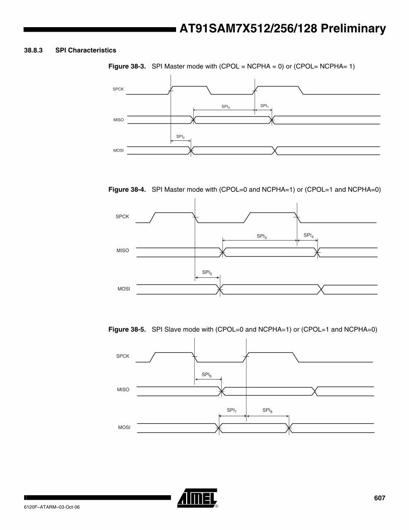
AT91SAM7X512/256/128 Preliminary
38.8.3 SPI Characteristics
Figure 38-3. SPI Master mode with (CPOL = NCPHA = 0) or (CPOL= NCPHA= 1)
Figure 38-4. SPI Master mode with (CPOL=0 and NCPHA=1) or (CPOL=1 and NCPHA=0)
Figure 38-5. SPI Slave mode with (CPOL=0 and NCPHA=1) or (CPOL=1 and NCPHA=0)
SPCK
MISO
MOSI
SPI2
SPI0 SPI1
SPCK
MISO
MOSI
SPI5
SPI3 SPI4
SPCK
MISO
MOSI
SPI6
SPI7 SPI8
6076120F–ATARM–03-Oct-06
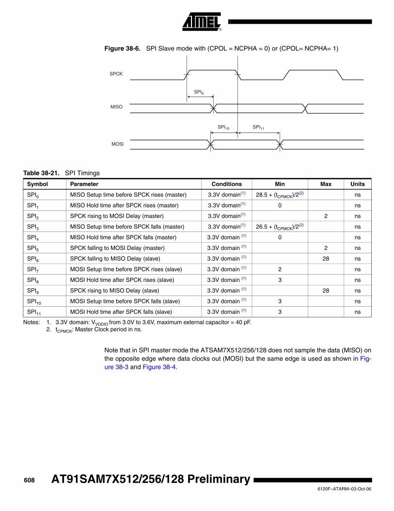
Figure 38-6. SPI Slave mode with (CPOL = NCPHA = 0) or (CPOL= NCPHA= 1)
Notes: 1. 3.3V domain: VVDDIO from 3.0V to 3.6V, maximum external capacitor = 40 pF. 2. tCPMCK: Master Clock period in ns.
Note that in SPI master mode the ATSAM7X512/256/128 does not sample the data (MISO) on the opposite edge where data clocks out (MOSI) but the same edge is used as shown in Fig-ure 38-3 and Figure 38-4.
SPCK
MISO
MOSI
SPI9
SPI10 SPI11
Table 38-21. SPI Timings
Symbol Parameter Conditions Min Max Units
SPI0 MISO Setup time before SPCK rises (master) 3.3V domain(1) 28.5 + (tCPMCK)/2(2) ns
SPI1 MISO Hold time after SPCK rises (master) 3.3V domain(1) 0 ns
SPI2 SPCK rising to MOSI Delay (master) 3.3V domain(1) 2 ns
SPI3 MISO Setup time before SPCK falls (master) 3.3V domain(1) 26.5 + (tCPMCK)/2(2) ns
SPI4 MISO Hold time after SPCK falls (master) 3.3V domain (1) 0 ns
SPI5 SPCK falling to MOSI Delay (master) 3.3V domain (1) 2 ns
SPI6 SPCK falling to MISO Delay (slave) 3.3V domain (1) 28 ns
SPI7 MOSI Setup time before SPCK rises (slave) 3.3V domain (1) 2 ns
SPI8 MOSI Hold time after SPCK rises (slave) 3.3V domain (1) 3 ns
SPI9 SPCK rising to MISO Delay (slave) 3.3V domain (1) 28 ns
SPI10 MOSI Setup time before SPCK falls (slave) 3.3V domain (1) 3 ns
SPI11 MOSI Hold time after SPCK falls (slave) 3.3V domain (1) 3 ns
6086120F–ATARM–03-Oct-06
AT91SAM7X512/256/128 Preliminary

AT91SAM7X512/256/128 Preliminary
38.8.4 EMAC Characteristics
Notes: 1. f: MCK frequency (MHz)2. VVDDIO from 3.0V to 3.6V, maximum external capacitor = 20 pF
Note: 1. VVDDIO from 3.0V to 3.6V, maximum external capacitor = 20 pF
Table 38-22. EMAC Signals
Symbol Parameter Conditions Min (ns) Max (ns)
EMAC1 Setup for EMDIO from EMDC rising Load: 20pF(2) 2
EMAC2 Hold for EMDIO from EMDC rising Load: 20pF(2) ((1/f)-19) + 4(1)
EMAC3 EMDIO toggling from EMDC falling Load: 20pF(2) 4.5
Table 38-23. EMAC MII Specific Signals
Symbol Parameter Conditions Min (ns) Max (ns)
EMAC4 Setup for ECOL from ETXCK rising Load: 20pF (1) 0
EMAC5 Hold for ECOL from ETXCK rising Load: 20pF (1) 2
EMAC6 Setup for ECRS from ETXCK rising Load: 20pF (1) 1.5
EMAC7 Hold for ECRS from ETXCK rising Load: 20pF (1) 2
EMAC8 ETXER toggling from ETXCK rising Load: 20pF (1) 25
EMAC9 ETXEN toggling from ETXCK rising Load: 20pF (1) 25
EMAC10 ETX toggling from ETXCK rising Load: 20pF (1) 25
EMAC11 Setup for ERX from ERXCK Load: 20pF (1) 0
EMAC12 Hold for ERX from ERXCK Load: 20pF (1) 4
EMAC13 Setup for ERXER from ERXCK Load: 20pF (1) 0
EMAC14 Hold for ERXER from ERXCK Load: 20pF (1) 4
EMAC15 Setup for ERXDV from ERXCK Load: 20pF (1) 2
EMAC16 Hold for ERXDV from ERXCK Load: 20pF (1) 2
6096120F–ATARM–03-Oct-06

Figure 38-7. EMAC MII Mode
EMDC
EMDIO
ECOL
ECRS
ETXCK
ETXER
ETXEN
ETX[3:0]
ERXCK
ERX[3:0]
ERXER
ERXDV
EMAC3EMAC1 EMAC2
EMAC4 EMAC5
EMAC6 EMAC7
EMAC8
EMAC9
EMAC10
EMAC11 EMAC12
EMAC13 EMAC14
EMAC15 EMAC16
6106120F–ATARM–03-Oct-06
AT91SAM7X512/256/128 Preliminary
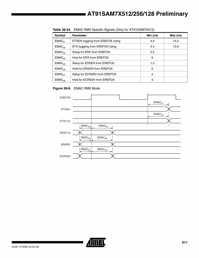
AT91SAM7X512/256/128 Preliminary
Figure 38-8. EMAC RMII Mode
Table 38-24. EMAC RMII Specific Signals (Only for AT91SAM7X512)
Symbol Parameter Min (ns) Max (ns)
EMAC21 ETXEN toggling from EREFCK rising 4.9 14.2
EMAC22 ETX toggling from EREFCK rising 4.4 15.9
EMAC23 Setup for ERX from EREFCK 0.5
EMAC24 Hold for ERX from EREFCK 0
EMAC25 Setup for ERXER from EREFCK 1.5
EMAC26 Hold for ERXER from EREFCK 0
EMAC27 Setup for ECRSDV from EREFCK 2
EMAC28 Hold for ECRSDV from EREFCK 0
EREFCK
ETXEN
ETX[1:0]
ERX[1:0]
ERXER
ECRSDV
EMAC21
EMAC22
EMAC23 EMAC24
EMAC25 EMAC26
EMAC27 EMAC28
6116120F–ATARM–03-Oct-06
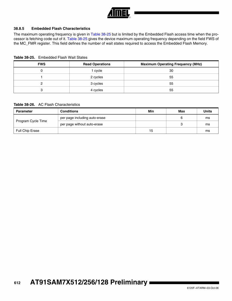
38.8.5 Embedded Flash Characteristics
The maximum operating frequency is given in Table 38-25 but is limited by the Embedded Flash access time when the pro-cessor is fetching code out of it. Table 38-25 gives the device maximum operating frequency depending on the field FWS of the MC_FMR register. This field defines the number of wait states required to access the Embedded Flash Memory.
Table 38-25. Embedded Flash Wait States
FWS Read Operations Maximum Operating Frequency (MHz)
0 1 cycle 30
1 2 cycles 55
2 3 cycles 55
3 4 cycles 55
Table 38-26. AC Flash Characteristics
Parameter Conditions Min Max Units
Program Cycle Timeper page including auto-erase 6 ms
per page without auto-erase 3 ms
Full Chip Erase 15 ms
6126120F–ATARM–03-Oct-06
AT91SAM7X512/256/128 Preliminary
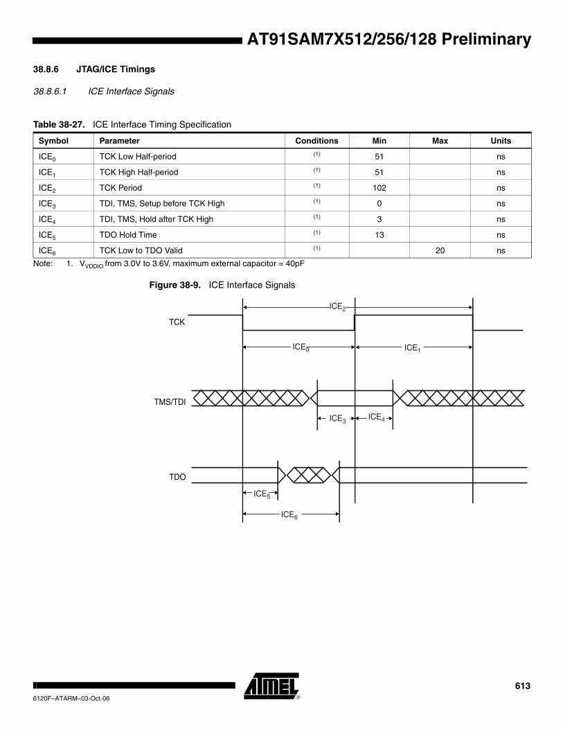
AT91SAM7X512/256/128 Preliminary
38.8.6 JTAG/ICE Timings
38.8.6.1 ICE Interface Signals
Note: 1. VVDDIO from 3.0V to 3.6V, maximum external capacitor = 40pF
Figure 38-9. ICE Interface Signals
Table 38-27. ICE Interface Timing Specification
Symbol Parameter Conditions Min Max Units
ICE0 TCK Low Half-period (1) 51 ns
ICE1 TCK High Half-period (1) 51 ns
ICE2 TCK Period (1) 102 ns
ICE3 TDI, TMS, Setup before TCK High (1) 0 ns
ICE4 TDI, TMS, Hold after TCK High (1) 3 ns
ICE5 TDO Hold Time (1) 13 ns
ICE6 TCK Low to TDO Valid (1) 20 ns
TCK
ICE3ICE4
ICE6
TMS/TDI
TDO
ICE5
ICE1
ICE2
ICE0
6136120F–ATARM–03-Oct-06

38.8.6.2 JTAG Interface Signals
Note: 1. VVDDIO from 3.0V to 3.6V, maximum external capacitor = 40pF
Figure 38-10. JTAG Interface Signals
Table 38-28. JTAG Interface Timing specification
Symbol Parameter Conditions Min Max Units
JTAG0 TCK Low Half-period (1) 6.5 ns
JTAG1 TCK High Half-period (1) 5.5 ns
JTAG2 TCK Period (1) 12 ns
JTAG3 TDI, TMS Setup before TCK High (1) 2 ns
JTAG4 TDI, TMS Hold after TCK High (1) 3 ns
JTAG5 TDO Hold Time (1) 4 ns
JTAG6 TCK Low to TDO Valid (1) 16 ns
JTAG7 Device Inputs Setup Time (1) 0 ns
JTAG8 Device Inputs Hold Time (1) 3 ns
JTAG9 Device Outputs Hold Time (1) 6 ns
JTAG10 TCK to Device Outputs Valid (1) 18 ns
TCK
JTAG9
TMS/TDI
TDO
Device Outputs
JTAG5
JTAG4JTAG3
JTAG0 JTAG1
JTAG2
JTAG10
Device Inputs
JTAG8JTAG7
JTAG6
6146120F–ATARM–03-Oct-06
AT91SAM7X512/256/128 Preliminary

AT91SAM7X512/256/128 Preliminary
39. AT91SAM7X512/256/128 Mechanical Characteristics
39.1 Thermal Considerations
39.1.1 Thermal DataTable 39-1 summarizes the thermal resistance data depending on the package.
39.1.2 Junction TemperatureThe average chip-junction temperature, TJ, in °C can be obtained from the following:
1.
2.
where:
• θJA = package thermal resistance, Junction-to-ambient (°C/W), provided in Table 39-1 on page 615.
• θJC = package thermal resistance, Junction-to-case thermal resistance (°C/W), provided in Table 39-1 on page 615.
• θHEAT SINK = cooling device thermal resistance (°C/W), provided in the device datasheet.
• PD = device power consumption (W) estimated from data provided in the section Section 38.3 ”Power Consumption” on page 598.
• TA = ambient temperature (°C).
Table 39-1. Thermal Resistance Data
Symbol Parameter Condition Package Typ Unit
θJA Junction-to-ambient thermal resistance Still Air LQFP100 38.3 °C/W
θJC Junction-to-case thermal resistance LQFP100 8.7
TJ TA PD θJA×( )+=
TJ TA P( D θ( HEATSINK× θJC ) )+ +=
6156120F–ATARM–03-Oct-06

39.2 Package Drawings
Figure 39-1. LQFP Package Drawing
6166120F–ATARM–03-Oct-06
AT91SAM7X512/256/128 Preliminary

AT91SAM7X512/256/128 Preliminary
Table 39-2. 100-lead LQFP Package Dimensions
Symbol
Millimeter Inch
Min Nom Max Min Nom Max
A 1.60 0.63
A1 0.05 0.15 0.002 0.006
A2 1.35 1.40 1.45 0.053 0.055 0.057
D 16.00 BSC 0.630 BSC
D1 14.00 BSC 0.551 BSC
E 16.00 BSC 0.630 BSC
E1 14.00 BSC 0.551 BSC
R2 0.08 0.20 0.003 0.008
R1 0.08 0.003
Q 0° 3.5° 7° 0° 3.5° 7°
θ1 0° 0°
θ2 11° 12° 13° 11° 12° 13°
θ3 11° 12° 13° 11° 12° 13°
c 0.09 0.20 0.004 0.008
L 0.45 0.60 0.75 0.018 0.024 0.030
L1 1.00 REF 0.039 REF
S 0.20 0.008
b 0.17 0.20 0.27 0.007 0.008 0.011
e 0.50 BSC 0.020 BSC
D2 12.00 0.472
E2 12.00 0.472
Tolerances of Form and Position
aaa 0.20 0.008
bbb 0.20 0.008
ccc 0.08 0.003
ddd 0.08 0.003
6176120F–ATARM–03-Oct-06

Figure 39-2. 100-TFBGA Package Drawing
This package respects the recommendations of the NEMI User Group.
All dimensions are in mm
Table 39-3. Device and LQFP Package Maximum Weight
AT91SAM7X512/256/128 800 mg
Table 39-4. Package Reference
JEDEC Drawing Reference MS-026
JESD97 Classification e2
Table 39-5. LQFP Package Characteristics
Moisture Sensitivity Level 3
6186120F–ATARM–03-Oct-06
AT91SAM7X512/256/128 Preliminary
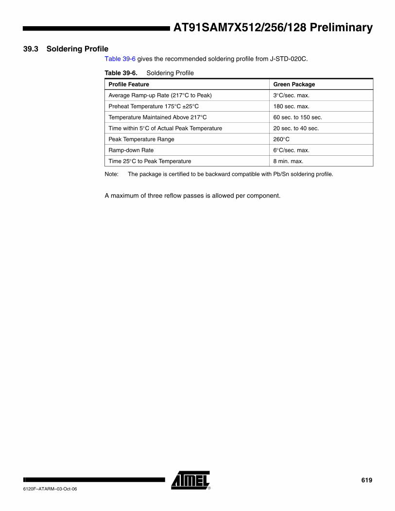
AT91SAM7X512/256/128 Preliminary
39.3 Soldering Profile Table 39-6 gives the recommended soldering profile from J-STD-020C.
Note: The package is certified to be backward compatible with Pb/Sn soldering profile.
A maximum of three reflow passes is allowed per component.
Table 39-6. Soldering Profile
Profile Feature Green Package
Average Ramp-up Rate (217°C to Peak) 3°C/sec. max.
Preheat Temperature 175°C ±25°C 180 sec. max.
Temperature Maintained Above 217°C 60 sec. to 150 sec.
Time within 5°C of Actual Peak Temperature 20 sec. to 40 sec.
Peak Temperature Range 260°C
Ramp-down Rate 6°C/sec. max.
Time 25°C to Peak Temperature 8 min. max.
6196120F–ATARM–03-Oct-06

40. AT91SAM7X Ordering Informationì
Table 40-1. Ordering Information
Ordering Code Package Package TypeTemperature
Operating Range
AT91SAM7X512-AUAT91SAM7X512-CU
LQFP 100TFBGA 100
GreenIndustrial
(-40°C to 85°C)
AT91SAM7X256-AUAT91SAM7X256-CU
LQFP 100TFBGA 100
GreenIndustrial
(-40°C to 85°C)
AT91SAM7X128-AUAT91SAM7X128-CU
LQFP 100TFBGA 100
GreenIndustrial
(-40°C to 85°C)
6206120F–ATARM–03-Oct-06
AT91SAM7X512/256/128 Preliminary
AT91SAM7X512/256/128 Preliminary
41. AT91SAM7X512/256/128 Errata
41.1 Marking
All devices are marked with the Atmel logo and the ordering code.
Additional marking has the following format:
where
• “YY”: manufactory year
• “WW”: manufactory week
• “V”: revision
• “XXXXXXXXX”: lot number
YYWW VXXXXXXXXX ARM
6216120F–ATARM–03-Oct-06
41.2 AT91SAM7X256/128 Errata - Rev. A Parts
Refer to Section 41.1 ”Marking”, on page 621.
41.2.1 Ethernet MAC (EMAC)
41.2.1.1 EMAC: RMII Mode
RMII mode is not functional.
Problem Fix/Workaround
None
41.2.1.2 EMAC: Possible Event Loss when Reading EMAC_ISR
If an event occurs within the same clock cycle in which the EMAC_ISR is read, the correspond-ing bit might be cleared even though it has not been read at 1. This might lead to the loss of this event.
Problem Fix/Workaround
Each time the software reads EMAC_ISR, it has to check the contents of the Transmit Status Register (EMAC_TSR), the Receive Status Register (EMAC_RSR) and the Network Status Register (EMAC_NSR), as the possible lost event is still notified in one of these registers.
41.2.1.3 EMAC: Possible Event Loss when Reading the Statistics Register Block
If an event occurs within the same clock cycle during which a statistics register is read, the cor-responding counter might lose this event. This might lead to the loss of the incrementation of one for this counter.
Problem Fix/Workaround
None
41.2.2 Peripheral Input/Output (PIO)
41.2.2.1 PIO: Leakage on PB27 - PB30
When PB27, PB28, PB29 or PB30 (the I/O lines multiplexed with the analog inputs) are set as digital inputs with pull-up disabled, the leakage can be 25 µA in worst case and 90 nA in typical case per I/O when the I/O is set externally at low level.
Problem Fix/Workaround
Set the I/O to VDDIO by internal or external pull-up.
41.2.2.2 PIO: Electrical Characteristics on NRST, PA0-PA30 and PB0-PB26
When NRST or PA0 - PA30 or PB0 - PB26 are set as digital inputs with pull-up enabled, the volt-age of the I/O stabilizes at VPull-up.
Vpull-up
VPull-up Min VPull-up Max
VDDIO - 0.65 V VDDIO - 0.45 V
6226120F–ATARM–03-Oct-06
AT91SAM7X512/256/128 Preliminary
AT91SAM7X512/256/128 Preliminary
This condition causes a leakage through VDDIO. This leakage is 45 µA per pad in worst case at 3.3 V.
Problem Fix/Workaround
It is recommended to use an external pull-up if needed.
41.2.2.3 PIO: Drive Low NRST, PA0-PA30 and PB0-PB26
When NRST or PA0 - PA30 or PB0 - PB26 are set as digital inputs with pull-up enabled, driving the I/O with an output impedance higher than 500 ohms may not drive the I/O to a logical zero.
Problem Fix/Workaround
Output impedance must be lower than 500 ohms.
41.2.3 Pulse Width Modulation Controller (PWM)
41.2.3.1 PWM: Update when PWM_CCNTx = 0 or 1
If the Channel Counter Register value is 0 or 1, the Channel Period Register or Channel Duty Cycle Register is directly modified when writing the Channel Update Register.
Problem Fix/Workaround
Check the Channel Counter Register before writing the update register.
41.2.3.2 PWM: Update when PWM_CPRDx = 0
When Channel Period Register equals 0, the period update is not operational.
Problem Fix/Workaround
Do not write 0 in the period register.
41.2.3.3 PWM: Counter Start Value
In left aligned mode, the first start value of the counter is 0. For the other periods, the counter starts at 1.
Problem Fix/Workaround
None.
41.2.3.4 PWM: Behavior of CHIDx Status Bits in the PWM_SR Register
Erratic behavior of the CHIDx status bit in the PWM_SR Register. When a channel is disabled by writing in the PWM_DIS Register just after enabling it (before completion of a Clock Period of the clock selected for the channel), the PWM line is internally disabled but the CHIDx status bit in the PWM_SR stays at 1.
Problem Fix/Workaround
Do not disable a channel before completion of one period of the selected clock.
I Leakage
Parameter Typ Max
I Leakage at 3,3V 2.5 µA 45 µA
6236120F–ATARM–03-Oct-06

41.2.4 Real Time Timer (RTT)
41.2.4.1 RTT: Possible Event Loss when Reading RTT_SRIf an event (RTTINC or ALMS) occurs within the same slow clock cycle during which the RTT_SR is read, the corresponding bit might be cleared. This can lead to the loss of this event.
Problem Fix/Workaround:
The software must handle the RTT event as an interrupt and should not poll RTT_SR.
41.2.5 Serial Peripheral Interface (SPI)
41.2.5.1 SPI: Bad tx_ready Behavior when CSAAT = 1 and SCBR = 1
If the SPI2 is programmed with CSAAT = 1, SCBR(baudrate) = 1 and two transfers are per-formed consecutively on the same slave with an IDLE state between them, the tx_ready signal does not rise after the second data has been transferred in the shifter. This can imply for exam-ple, that the second data is sent twice.
Problem Fix/Workaround
Do not use the combination CSAAT = 1 and SCBR = 1.
41.2.5.2 SPI: LASTXFER (Last Transfer) Behavior
In FIXED Mode, with CSAAT bit set, and in “PDC mode” the Chip Select can rise depending on the data written in the SPI_TDR when the TX_EMPTY flag is set. If for example, the PDC writes a “1” in the bit 24 (LASTXFER bit) of the SPI_TDR, the chip select will rise as soon as the TXEMPTY flag is set.
Problem Fix/Workaround
Use the CS in PIO mode when PDC mode is required and CS has to be maintained between transfers.
41.2.5.3 SPI: SPCK Behavior in Master Mode
SPCK pin can toggle out before the first transfer in Master Mode.
Problem Fix/Workaround
In Master Mode, MSTR bit must be set (in SPI_MR register) before configuring SPI_CSRx registers.
41.2.5.4 SPI: Chip Select and Fixed Mode
In fixed Mode, if a transfer is performed through a PDC on a Chip select different from the Chip select 0, the output spi_size sampled by the PDC will depend on the field, BITS (Bits per Trans-fer) of SPI_CSR0 register, whatever the selected Chip select is. For example, if SPI_CSR0 is configured for a 10-bit transfer whereas SPI_CSR1 is configured for an 8-bit transfer, when a transfer is performed in Fixed mode through the PDC, on Chip select 1, the transfer will be con-sidered as a HalfWord transfer.
Problem Fix/Workaround
If a PDC transfer has to be performed in 8 bits, on a Chip select y (y as different from 0), the BITS field of the SPI_CSR0 must be configured in 8 bits, in the same way as the BITS field of the CSRy Register.
6246120F–ATARM–03-Oct-06
AT91SAM7X512/256/128 Preliminary
AT91SAM7X512/256/128 Preliminary
41.2.5.5 SPI: Baudrate Set to 1When Baudrate is set at 1 (i.e. when serial clock frequency equals the system clock frequency) and when the BITS field of the SPI_CSR register (number of bits to be transmitted) equals an ODD value (in this case 9,11,13 or 15), an additional pulse will be generated on output SPCK.
Everything is OK if the BITS field equals 8,10,12,14 or 16 and Baudrate = 1.
Problem Fix/Workaround
None.
41.2.6 Synchronous Serial Controller (SSC)
41.2.6.1 SSC: Periodic Transmission Limitations in Master Mode
If the Least Significant Bit is sent first (MSBF = 0), the first TAG during the frame synchro is not sent.
Problem Fix/Workaround
None.
41.2.6.2 SSC: Transmitter Limitations in Slave Mode
If TK is programmed as output and TF is programmed as input, it is impossible to emit data when the start of edge (rising or falling) of synchro has a Start Delay equal to zero.
Problem Fix/Workaround
None.
41.2.6.3 SSC: Transmitter Limitations in Slave Mode
If TK is programmed as an input and TF is programmed as an output and requested to be set to low/high during data emission, the Frame Synchro signal is generated one bit clock period after the data start and one data bit is lost. This problem does not exist when generating a periodic synchro.
Problem Fix/Workaround
The data need to be delayed for one bit clock period with an external assembly. In the following schematic, TD, TK and NRST are AT91SAM7X signals, TXD is the delayed data to connect to the device.
6256120F–ATARM–03-Oct-06

41.2.7 Two-wire Interface (TWI)
41.2.7.1 TWI: Clock Divider
The value of CLDIV x 2CKDIV must be less than or equal to 8191, the value of CHDIV x 2CKDIV
must be less than or equal to 8191⋅
Problem Fix/Workaround
None.
41.2.7.2 TWI: Disabling Does not Operate Correctly
Any transfer in progress is immediately frozen if the Control Register (TWI_CR) is written with the bit MSDIS at 1. Furthermore, the status bits TXCOMP and TXRDY in the Status Register (TWI_SR) are not reset.
Problem Fix/Workaround
The user must wait for the end of transfer before disabling the TWI. In addition, the interrupts must be disabled before disabling the TWI.
41.2.7.3 TWI: NACK Status Bit Lost
During a master frame, if TWI_SR is read between the Non Acknowledge condition detection and the TXCOMP bit rising in the TWI_SR, the NACK bit is not set.
Problem Fix/Workaround
The user must wait for the TXCOMP status bit by interrupt and must not read the TWI_SR as long as transmission is not completed.
TXCOMP and NACK fields are set simultaneously and the NACK field is reset after the read of the TWI_SR.
6266120F–ATARM–03-Oct-06
AT91SAM7X512/256/128 Preliminary

AT91SAM7X512/256/128 Preliminary
41.2.7.4 TWI: Possible Receive Holding Register Corruption
When loading the TWI_RHR, the transfer direction is ignored. The last data byte received in the TWI_RHR is corrupted at the end of the first subsequent transmit data byte. Neither RXRDY nor OVERRUN status bits are set if this occurs.
Problem Fix/Workaround
The user must be sure that received data is read before transmitting any new data.
41.2.7.5 TWI: Software Resetwhen a software reset is performed during a frame and when TWCK is low, it is impossible to ini-tiate a new transfer in READ or WRITE mode.
Problem Fix/Workaround
None.
41.2.8 Universal Synchronous Asynchronous Receiver Transmitter (USART)
41.2.8.1 USART: CTS in Hardware Handshaking
When Hardware Handshaking is used and if CTS goes low close to the end of the starting bit, a character can be lost.
Problem Fix/Workaround
CTS must not go low during a time slot occurring between 2 Master Clock periods before the starting bit and 16 Master Clock periods after the rising edge of the starting bit.
41.2.8.2 USART: Hardware Handshaking – Two Characters SentIf CTS switches from 0 to 1 during the TX of a character and if the holding register (US_THR) is not empty, the content of US_THR will also be transmitted.
Problem Fix/WorkaroundDon't use the PDC in transmit mode and do not fill US_THR before TXEMPTY is set at 1.
41.2.8.3 USART: XOFF Character Bad BehaviorThe XOFF character is sent only when the receive buffer is detected full. While the XOFF is being sent, the remote transmitter is still transmitting. As only one Holding register is available in the receiver, characters will be lost in reception. This makes the software handshaking function-ality ineffective.
Problem Fix/Workaround
None.
6276120F–ATARM–03-Oct-06
41.3 AT91SAM7X512 Errata - Rev. A Parts
Refer to Section 41.1 ”Marking”, on page 621.
41.3.1 Ethernet MAC (EMAC)
41.3.1.1 EMAC: Possible Event Loss when Reading EMAC_ISR
If an event occurs within the same clock cycle in which the EMAC_ISR is read, the correspond-ing bit might be cleared even though it has not been read at 1. This might lead to the loss of this event.
Problem Fix/Workaround
Each time the software reads EMAC_ISR, it has to check the contents of the Transmit Status Register (EMAC_TSR), the Receive Status Register (EMAC_RSR) and the Network Status Register (EMAC_NSR), as the possible lost event is still notified in one of these registers.
41.3.1.2 EMAC: Possible Event Loss when Reading the Statistics Register Block
If an event occurs within the same clock cycle during which a statistics register is read, the cor-responding counter might lose this event. This might lead to the loss of the incrementation of one for this counter.
Problem Fix/Workaround
None
41.3.2 Peripheral Input/Output (PIO)
41.3.2.1 PIO: Leakage on PB27 - PB30
When PB27, PB28, PB29 or PB30 (the I/O lines multiplexed with the analog inputs) are set as digital inputs with pull-up disabled, the leakage can be 25 µA in worst case and 90 nA in typical case per I/O when the I/O is set externally at low level.
Problem Fix/Workaround
Set the I/O to VDDIO by internal or external pull-up.
41.3.2.2 PIO: Electrical Characteristics on NRST, PA0-PA30 and PB0-PB26
When NRST or PA0 - PA30 or PB0 - PB26 are set as digital inputs with pull-up enabled, the volt-age of the I/O stabilizes at VPull-up.
This condition causes a leakage through VDDIO. This leakage is 45 µA per pad in worst case at 3.3 V.
Vpull-up
VPull-up Min VPull-up Max
VDDIO - 0.65 V VDDIO - 0.45 V
I Leakage
Parameter Typ Max
I Leakage at 3,3V 2.5 µA 45 µA
6286120F–ATARM–03-Oct-06
AT91SAM7X512/256/128 Preliminary

AT91SAM7X512/256/128 Preliminary
Problem Fix/Workaround
It is recommended to use an external pull-up if needed.
41.3.2.3 PIO: Drive Low NRST, PA0-PA30 and PB0-PB26
When NRST or PA0 - PA30 or PB0 - PB26 are set as digital inputs with pull-up enabled, driving the I/O with an output impedance higher than 500 ohms may not drive the I/O to a logical zero.
Problem Fix/Workaround
Output impedance must be lower than 500 ohms.
41.3.3 Pulse Width Modulation Controller (PWM)
41.3.3.1 PWM: Update when PWM_CCNTx = 0 or 1
If the Channel Counter Register value is 0 or 1, the Channel Period Register or Channel Duty Cycle Register is directly modified when writing the Channel Update Register.
Problem Fix/Workaround
Check the Channel Counter Register before writing the update register.
41.3.3.2 PWM: Update when PWM_CPRDx = 0
When Channel Period Register equals 0, the period update is not operational.
Problem Fix/Workaround
Do not write 0 in the period register.
41.3.3.3 PWM: Counter Start Value
In left aligned mode, the first start value of the counter is 0. For the other periods, the counter starts at 1.
Problem Fix/Workaround
None.
41.3.3.4 PWM: Behavior of CHIDx Status Bits in the PWM_SR Register
Erratic behavior of the CHIDx status bit in the PWM_SR Register. When a channel is disabled by writing in the PWM_DIS Register just after enabling it (before completion of a Clock Period of the clock selected for the channel), the PWM line is internally disabled but the CHIDx status bit in the PWM_SR stays at 1.
Problem Fix/Workaround
Do not disable a channel before completion of one period of the selected clock.
41.3.4 Real Time Timer (RTT)
41.3.4.1 RTT: Possible Event Loss when Reading RTT_SRIf an event (RTTINC or ALMS) occurs within the same slow clock cycle during which the RTT_SR is read, the corresponding bit might be cleared. This can lead to the loss of this event.
Problem Fix/Workaround:
The software must handle the RTT event as an interrupt and should not poll RTT_SR.
6296120F–ATARM–03-Oct-06

41.3.5 Serial Peripheral Interface (SPI)
41.3.5.1 SPI: Bad tx_ready Behavior when CSAAT = 1 and SCBR = 1
If the SPI2 is programmed with CSAAT = 1, SCBR(baudrate) = 1 and two transfers are per-formed consecutively on the same slave with an IDLE state between them, the tx_ready signal does not rise after the second data has been transferred in the shifter. This can imply for exam-ple, that the second data is sent twice.
Problem Fix/Workaround
Do not use the combination CSAAT = 1 and SCBR = 1.
41.3.5.2 SPI: LASTXFER (Last Transfer) Behavior
In FIXED Mode, with CSAAT bit set, and in “PDC mode” the Chip Select can rise depending on the data written in the SPI_TDR when the TX_EMPTY flag is set. If for example, the PDC writes a “1” in the bit 24 (LASTXFER bit) of the SPI_TDR, the chip select will rise as soon as the TXEMPTY flag is set.
Problem Fix/Workaround
Use the CS in PIO mode when PDC mode is required and CS has to be maintained between transfers.
41.3.5.3 SPI: SPCK Behavior in Master Mode
SPCK pin can toggle out before the first transfer in Master Mode.
Problem Fix/Workaround
In Master Mode, MSTR bit must be set (in SPI_MR register) before configuring SPI_CSRx registers.
41.3.5.4 SPI: Chip Select and Fixed Mode
In fixed Mode, if a transfer is performed through a PDC on a Chip select different from the Chip select 0, the output spi_size sampled by the PDC will depend on the field, BITS (Bits per Trans-fer) of SPI_CSR0 register, whatever the selected Chip select is. For example, if SPI_CSR0 is configured for a 10-bit transfer whereas SPI_CSR1 is configured for an 8-bit transfer, when a transfer is performed in Fixed mode through the PDC, on Chip select 1, the transfer will be con-sidered as a HalfWord transfer.
Problem Fix/Workaround
If a PDC transfer has to be performed in 8 bits, on a Chip select y (y as different from 0), the BITS field of the SPI_CSR0 must be configured in 8 bits, in the same way as the BITS field of the CSRy Register.
41.3.5.5 SPI: Baudrate Set to 1When Baudrate is set at 1 (i.e. when serial clock frequency equals the system clock frequency) and when the BITS field of the SPI_CSR register (number of bits to be transmitted) equals an ODD value (in this case 9,11,13 or 15), an additional pulse will be generated on output SPCK.
Everything is OK if the BITS field equals 8,10,12,14 or 16 and Baudrate = 1.
Problem Fix/Workaround
None.
6306120F–ATARM–03-Oct-06
AT91SAM7X512/256/128 Preliminary
AT91SAM7X512/256/128 Preliminary
41.3.6 Synchronous Serial Controller (SSC)
41.3.6.1 SSC: Periodic Transmission Limitations in Master Mode
If the Least Significant Bit is sent first (MSBF = 0), the first TAG during the frame synchro is not sent.
Problem Fix/Workaround
None.
41.3.6.2 SSC: Transmitter Limitations in Slave Mode
If TK is programmed as output and TF is programmed as input, it is impossible to emit data when the start of edge (rising or falling) of synchro has a Start Delay equal to zero.
Problem Fix/Workaround
None.
41.3.6.3 SSC: Transmitter Limitations in Slave Mode
If TK is programmed as an input and TF is programmed as an output and requested to be set to low/high during data emission, the Frame Synchro signal is generated one bit clock period after the data start and one data bit is lost. This problem does not exist when generating a periodic synchro.
Problem Fix/Workaround
The data need to be delayed for one bit clock period with an external assembly. In the following schematic, TD, TK and NRST are AT91SAM7X signals, TXD is the delayed data to connect to the device.
6316120F–ATARM–03-Oct-06

41.3.7 Two-wire Interface (TWI)
41.3.7.1 TWI: Clock Divider
The value of CLDIV x 2CKDIV must be less than or equal to 8191, the value of CHDIV x 2CKDIV
must be less than or equal to 8191⋅
Problem Fix/Workaround
None.
41.3.7.2 TWI: Disabling Does not Operate Correctly
Any transfer in progress is immediately frozen if the Control Register (TWI_CR) is written with the bit MSDIS at 1. Furthermore, the status bits TXCOMP and TXRDY in the Status Register (TWI_SR) are not reset.
Problem Fix/Workaround
The user must wait for the end of transfer before disabling the TWI. In addition, the interrupts must be disabled before disabling the TWI.
41.3.7.3 TWI: NACK Status Bit Lost
During a master frame, if TWI_SR is read between the Non Acknowledge condition detection and the TXCOMP bit rising in the TWI_SR, the NACK bit is not set.
Problem Fix/Workaround
The user must wait for the TXCOMP status bit by interrupt and must not read the TWI_SR as long as transmission is not completed.
TXCOMP and NACK fields are set simultaneously and the NACK field is reset after the read of the TWI_SR.
41.3.7.4 TWI: Possible Receive Holding Register Corruption
When loading the TWI_RHR, the transfer direction is ignored. The last data byte received in the TWI_RHR is corrupted at the end of the first subsequent transmit data byte. Neither RXRDY nor OVERRUN status bits are set if this occurs.
Problem Fix/Workaround
The user must be sure that received data is read before transmitting any new data.
41.3.7.5 TWI: Software Resetwhen a software reset is performed during a frame and when TWCK is low, it is impossible to ini-tiate a new transfer in READ or WRITE mode.
Problem Fix/Workaround
None.
6326120F–ATARM–03-Oct-06
AT91SAM7X512/256/128 Preliminary
AT91SAM7X512/256/128 Preliminary
41.3.8 Universal Synchronous Asynchronous Receiver Transmitter (USART)
41.3.8.1 USART: CTS in Hardware Handshaking
When Hardware Handshaking is used and if CTS goes low close to the end of the starting bit, a character can be lost.
Problem Fix/Workaround
CTS must not go low during a time slot occurring between 2 Master Clock periods before the starting bit and 16 Master Clock periods after the rising edge of the starting bit.
41.3.8.2 USART: Hardware Handshaking – Two Characters SentIf CTS switches from 0 to 1 during the TX of a character and if the holding register (US_THR) is not empty, the content of US_THR will also be transmitted.
Problem Fix/WorkaroundDon't use the PDC in transmit mode and do not fill US_THR before TXEMPTY is set at 1.
41.3.8.3 USART: XOFF Character Bad BehaviorThe XOFF character is sent only when the receive buffer is detected full. While the XOFF is being sent, the remote transmitter is still transmitting. As only one Holding register is available in the receiver, characters will be lost in reception. This makes the software handshaking function-ality ineffective.
Problem Fix/Workaround
None.
6336120F–ATARM–03-Oct-06

6346120F–ATARM–03-Oct-06
AT91SAM7X512/256/128 Preliminary

AT91SAM7X512/256/128 Preliminary
42. Revision History
Version Comments
Change Request Ref.
6120A 10-Oct-05 First issue
6120B 17-Oct-05
Updated product functionalities in ”Features” on page 1, Figure 2-1 on page 4, Section 9.5 ”Debug Unit” on page 29, and Figure 11-1 on page 27
05-456
Corrected PLL output range maximum value in Section 9.2 ”Clock Generator” on page 27, Figure 18-3 in Section 18.3.2.1 ”Internal Memory Mapping” on page 93 and Table 38-12, “Phase Lock Loop Characteristics,” on page 602.
05-491Updated information in Power Supplies on page 9
Updated field Part Number in Section 12.5.5 ”ID Code Register” on page 55.
Updated Chip ID in Section 9.5 ”Debug Unit” on page 29 and in Section 12.5.3 ”Debug Unit” on page 48. 05-472
Removed references to PGMEN2 in Section 20. ”Fast Flash Programming Interface (FFPI)” on page 117. 05-464
Updated “ARCH: Architecture Identifier” in Debug Unit with new values for AT91SAM7XCxx series and AT91SAM7Xxx series.
05-459
Updated CAN bit timing configuration in Section 36.6.4.1 ”CAN Bit Timing Configuration” on page 502 and in Section 36.8.6 ”CAN Baudrate Register” on page 533.
05-419
Added Section 38.8.4 ”EMAC Characteristics” on page 609. 05-469
Updated AT91SAM7X Ordering information. 05-470
6120C 26-Oct-05
Replaced Section 29. ”Two-wire Interface (TWI)” on page 279. 05-516
6120D 03-Feb-06
Section 41. ”AT91SAM7X512/256/128 Errata”Device package/product number changed
Section 41.2.1 ”Ethernet MAC (EMAC)” RMII mode is not functional
The sections listed below have been added to the Errata:Section 41.2.3 ”Pulse Width Modulation Controller (PWM)”
Section 41.2.5 ”Serial Peripheral Interface (SPI)”
Section 41.2.6 ”Synchronous Serial Controller (SSC)”Section 41.2.7 ”Two-wire Interface (TWI)”
Section 41.2.8 ”Universal Synchronous Asynchronous Receiver Transmitter (USART)”
#1767
6120E 04-Apr-06
The following errata have been added:Section 41.2.1.2 ”EMAC: Possible Event Loss when Reading EMAC_ISR”
Section 41.2.1.3 ”EMAC: Possible Event Loss when Reading the Statistics Register Block”
Section 41.2.5.3 ”SPI: SPCK Behavior in Master Mode”
Section 41.2.2.1 ”PIO: Leakage on PB27 - PB30”: worst case leakage changed to 9 µA
#2455
#2605
6356120F–ATARM–03-Oct-06

Version6120F Comments
Change Request Ref.
AT91SAM7X512 added to product family. ”Features” on page 1, ”Description” on page 3 Global and TFBGA package to Section 4. ”Package”, Section 39. ”AT91SAM7X512/256/128 Mechanical Characteristics” and Section 40. ”AT91SAM7X Ordering Informationì”.
Section 4.1 ”100-lead LQFP Package Outline” and Section 4.3 ”100-ball TFBGA Package Outline” Replace “...Mechanical Overview”
Peripheral and System Controller Memory Maps consolidated in Figure 8-1 on page 18
Internal Memory Area 3 is “Internal ROM” Figure 18-3 on page 93
#2724
Section 10.1 ”User Interface” User Peripherals are mapped between 0xF000 0000 and 0XFFFF EFFF.
Table 10-1 on page 31 SYSIRQ changed to SYSC in “Peripheral Identifiers”.rfo review
IP Block Evolution:
RSTC: Section 13.3 ”Functional Description” on page 58, added information on startup counter for crystal oscillator.
3005
RTT: Section 14.3 ”Functional Description”: Note (asynchronization between SCLK and MCK) added to end of section.
2522
WDT: ”Block Diagram” on page 83 replaced. (WV changed to WDV) ”Functional Description” on page 84 6th and 7th paragraph changed.
3002
EFC: Section 19. ”Embedded Flash Controller (EFC)” updated to reflect EFC configuration for AT91SAM7X512 with multiple EFCs.
2356
3086
FFPI: information added to Section 20.2.5.6 and Section 20.3.4.6 ”Flash Security Bit Command”, added Section 20.2.5.7 and Section 20.3.4.7 ”AT91SAM7X512 Select EFC Command”
rfo/2284
AT91SAM Boot Program: ”Hardware and Software Constraints” on page 138 SAM7X512 added
”SAM-BA Boot” on page 134, SAM-BA boot principle changed”Flow Diagram” on page 133 replaced Figure 21-1
2285/2618
3050
PDC: Corrected description of user interface in Section 22.1 ”Overview” on page 139. Corrected bit name to ENDTX in Section 22.3.3 ”Transfer Counters” on page 140. 05-460
AIC: Section 23.7.3.1 ”Priority Controller” on page 156: incorrect reference of SRCTYPE field to AIC_SVR register changed to AIC_SMR register. Section 23.8 ”Advanced Interrupt Controller (AIC) User Interface” on page 164, Table 23-2: Added note (2) in reference to PID2...PID31 bit fields. Naming convention for AIC_FVR register harmonized in Table 23-2, Section 23.8.6 ”AIC FIQ Vector Register” on page 167 and Section 23.7.4.5 ”Fast Forcing” on page 160.
2512
2548
PMC: Section 25.7 ”Programming Sequence” on page 181 change to Step 4. on page 182, “Selection of Master Clock and Processor Clock” and to code. Corrected name of bitfield PRES in Section 25.9.10 ”PMC Master Clock Register” on page 197.
Removed reference to PMC_ACKR register in Table 25-2, “Register Mapping,” on page 188.
Updated OUTx bit descriptions in Section 25.9.9 ”PMC Clock Generator PLL Register” on page 196. Added note defining PIDx in Section 25.9.4 ”PMC Peripheral Clock Enable Register” on page 192, Section 25.9.5 ”PMC Peripheral Clock Disable Register” on page 192 and Section 25.9.6 ”PMC Peripheral Clock Status Register” on page 193.
Changed Section 24.2 ”Slow Clock RC Oscillator” on page 175.
05-506
16031719
2467, 2913
2468
1558
DBGU: Corrected references from ice_nreset to Power-on Reset in Figure 26-1 on page 204, Functional Block Diagram, and in FNTRST bit description in Section 26.5.12 ”Debug Unit Force NTRST Register” on page 226.
2832
6366120F–ATARM–03-Oct-06
AT91SAM7X512/256/128 Preliminary
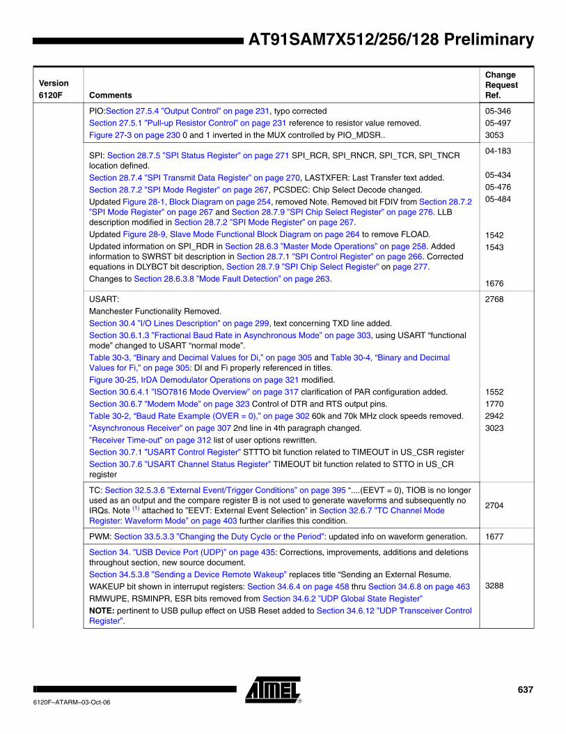
AT91SAM7X512/256/128 Preliminary
PIO:Section 27.5.4 ”Output Control” on page 231, typo correctedSection 27.5.1 ”Pull-up Resistor Control” on page 231 reference to resistor value removed.
Figure 27-3 on page 230 0 and 1 inverted in the MUX controlled by PIO_MDSR..
05-34605-497
3053
SPI: Section 28.7.5 ”SPI Status Register” on page 271 SPI_RCR, SPI_RNCR, SPI_TCR, SPI_TNCR location defined.
Section 28.7.4 ”SPI Transmit Data Register” on page 270, LASTXFER: Last Transfer text added.
Section 28.7.2 ”SPI Mode Register” on page 267, PCSDEC: Chip Select Decode changed.Updated Figure 28-1, Block Diagram on page 254, removed Note. Removed bit FDIV from Section 28.7.2 ”SPI Mode Register” on page 267 and Section 28.7.9 ”SPI Chip Select Register” on page 276. LLB description modified in Section 28.7.2 ”SPI Mode Register” on page 267.
Updated Figure 28-9, Slave Mode Functional Block Diagram on page 264 to remove FLOAD. Updated information on SPI_RDR in Section 28.6.3 ”Master Mode Operations” on page 258. Added information to SWRST bit description in Section 28.7.1 ”SPI Control Register” on page 266. Corrected equations in DLYBCT bit description, Section 28.7.9 ”SPI Chip Select Register” on page 277.
Changes to Section 28.6.3.8 ”Mode Fault Detection” on page 263.
04-183
05-434
05-47605-484
1542
1543
1676
USART:
Manchester Functionality Removed.
Section 30.4 ”I/O Lines Description” on page 299, text concerning TXD line added. Section 30.6.1.3 ”Fractional Baud Rate in Asynchronous Mode” on page 303, using USART “functional mode” changed to USART “normal mode”.Table 30-3, “Binary and Decimal Values for Di,” on page 305 and Table 30-4, “Binary and Decimal Values for Fi,” on page 305: DI and Fi properly referenced in titles.Figure 30-25, IrDA Demodulator Operations on page 321 modified.
Section 30.6.4.1 ”ISO7816 Mode Overview” on page 317 clarification of PAR configuration added.
Section 30.6.7 ”Modem Mode” on page 323 Control of DTR and RTS output pins.Table 30-2, “Baud Rate Example (OVER = 0),” on page 302 60k and 70k MHz clock speeds removed.
”Asynchronous Receiver” on page 307 2nd line in 4th paragraph changed.
”Receiver Time-out” on page 312 list of user options rewritten.Section 30.7.1 ”USART Control Register” STTTO bit function related to TIMEOUT in US_CSR register
Section 30.7.6 ”USART Channel Status Register” TIMEOUT bit function related to STTO in US_CR register
2768
1552
17702942
3023
TC: Section 32.5.3.6 ”External Event/Trigger Conditions” on page 395 “....(EEVT = 0), TIOB is no longer used as an output and the compare register B is not used to generate waveforms and subsequently no IRQs. Note (1) attached to ”EEVT: External Event Selection” in Section 32.6.7 ”TC Channel Mode Register: Waveform Mode” on page 403 further clarifies this condition.
2704
PWM: Section 33.5.3.3 ”Changing the Duty Cycle or the Period”: updated info on waveform generation. 1677
Section 34. ”USB Device Port (UDP)” on page 435: Corrections, improvements, additions and deletions throughout section, new source document.Section 34.5.3.8 ”Sending a Device Remote Wakeup” replaces title “Sending an External Resume.
WAKEUP bit shown in interruput registers: Section 34.6.4 on page 458 thru Section 34.6.8 on page 463
RMWUPE, RSMINPR, ESR bits removed from Section 34.6.2 ”UDP Global State Register”
NOTE: pertinent to USB pullup effect on USB Reset added to Section 34.6.12 ”UDP Transceiver Control Register”.
3288
Version6120F Comments
Change Request Ref.
6376120F–ATARM–03-Oct-06

ADC: Section 35-1 ”Analog-to-Digital Converter Block Diagram” on page 471 dedicated and I/O line multiplexed inputs differentiated.”ADC Timings” on page 478 typo corrected in warning
3052
2830
CAN: Update to message acceptance example in Section 36.6.2.1 ”Message Acceptance Procedure” on page 494.
New information on byte priority added to Section 36.8.17 ”CAN Message Data Low Register” on page 542 and Section 36.8.18 ”CAN Message Data High Register” on page 543.
Corrected MDL bit description in Section 36.8.17 ”CAN Message Data Low Register” on page 542.Update to specify allowed values for BRP field on Section 36.6.4 ”CAN 2.0 Standard Features”, page 499 and in Section 36.8.6 ”CAN Baudrate Register” on page 529.
2295, 2296
2476
2597
EMAC: ”Interrupt Enable Register” on page 573, access changed to Write-only.
”Interrupt Disable Register” on page 574, access changed to Write-only. ”Interrupt Mask Register” on page 575, access changed to Read-only.
1725
Section 38. ”AT91SAM7X Electrical Characteristics””Absolute Maximum Ratings” on page 595 change to Maximum Operating Voltages 3059
Changed conditions of parameters IPULLUP and ILEAK in Table 38-2, “DC Characteristics,” on page 596.Updated Table 38-5, “DC Flash Characteristics AT91SAM7X512/256/128,” on page 597 and Table 38-9, “Main Oscillator Characteristics,” on page 600.Added Table 38-10, “Crystal Characteristics,” on page 601.
Updated IDDBP in Table 38-11, “XIN Clock Electrical Characteristics,” on page 601.
Added information on data sampling in SPI master mode to Table 38-21, “SPI Timings,” on page 608.Updated Table 38-22, “EMAC Signals,” on page 609
Added Table 38-24, “EMAC RMII Specific Signals (Only for AT91SAM7X512),” on page 611 and Figure 38-8, EMAC RMII Mode on page 611.
rfo review
Errata updated:Added Section 41.1 ”Marking” on page 621.
Section 41.2.4.1 ”RTT: Possible Event Loss when Reading RTT_SR”
Section 41.2.5.4 ”SPI: Chip Select and Fixed Mode”Section 41.2.5.5 ”SPI: Baudrate Set to 1”
TWI: Behavior of OVRE Bit (removed)
Section 41.2.7.5 ”TWI: Software Reset”Section 41.2.8.2 ”USART: Hardware Handshaking – Two Characters Sent”
Section 41.2.8.3 ”USART: XOFF Character Bad Behavior”
#2871
PIO: Leakage on PB27 - PB 30 ....”the leakage can be 25 µA in worst case...” rfo review
Version6120F Comments
Change Request Ref.
6386120F–ATARM–03-Oct-06
AT91SAM7X512/256/128 Preliminary

AT91SAM7X512/256/128 Preliminary
Table of Contents
Features ..................................................................................................... 1
1 Description ............................................................................................... 3
1.1 Configuration Summary of the AT91SAM7X512/256/128 ........................................3
2 AT91SAM7X512/256/128 Block Diagram ................................................ 4
3 Signal Description ................................................................................... 5
4 Package .................................................................................................... 8
4.1 100-lead LQFP Package Outline ..............................................................................8
4.2 100-lead LQFP Pinout .............................................................................................9
4.3 100-ball TFBGA Package Outline ..........................................................................10
4.4 100-ball TFBGA Pinout ..........................................................................................10
5 Power Considerations ........................................................................... 11
5.1 Power Supplies ......................................................................................................11
5.2 Power Consumption ...............................................................................................11
5.3 Voltage Regulator ...................................................................................................11
5.4 Typical Powering Schematics ................................................................................12
6 I/O Lines Considerations ....................................................................... 13
6.1 JTAG Port Pins .......................................................................................................13
6.2 Test Pin ..................................................................................................................13
6.3 Reset Pin ................................................................................................................13
6.4 ERASE Pin .............................................................................................................13
6.5 PIO Controller Lines ...............................................................................................13
6.6 I/O Lines Current Drawing ......................................................................................14
7 Processor and Architecture .................................................................. 15
7.1 ARM7TDMI Processor ...........................................................................................15
7.2 Debug and Test Features .......................................................................................15
7.3 Memory Controller ..................................................................................................15
7.4 Peripheral DMA Controller .....................................................................................16
8 Memories ................................................................................................ 17
8.1 AT91SAM7X512 .....................................................................................................17
8.2 AT91SAM7X256 .....................................................................................................17
8.3 AT91SAM7X128 .....................................................................................................17
8.4 Memory Mapping ....................................................................................................19
i6120F–ATARM–03-Oct-06
8.5 Embedded Flash ....................................................................................................20
8.6 Fast Flash Programming Interface .........................................................................22
8.7 SAM-BA Boot Assistant ..........................................................................................22
9 System Controller .................................................................................. 24
9.1 Reset Controller .....................................................................................................26
9.2 Clock Generator .....................................................................................................27
9.3 Power Management Controller ...............................................................................28
9.4 Advanced Interrupt Controller ................................................................................28
9.5 Debug Unit .............................................................................................................29
9.6 Periodic Interval Timer ...........................................................................................29
9.7 Watchdog Timer .....................................................................................................29
9.8 Real-time Timer ......................................................................................................30
9.9 PIO Controllers .......................................................................................................30
9.10 Voltage Regulator Controller ................................................................................30
10 Peripherals ............................................................................................. 31
10.1 User Interface .......................................................................................................31
10.2 Peripheral Identifiers ............................................................................................31
10.3 Peripheral Multiplexing on PIO Lines ...................................................................32
10.4 PIO Controller A Multiplexing ...............................................................................33
10.5 PIO Controller B Multiplexing ...............................................................................34
10.6 Ethernet MAC .......................................................................................................35
10.7 Serial Peripheral Interface ....................................................................................35
10.8 Two-wire Interface ................................................................................................35
10.9 USART .................................................................................................................36
10.10 Serial Synchronous Controller ............................................................................36
10.11 Timer Counter ....................................................................................................36
10.12 Pulse Width Modulation Controller .....................................................................37
10.13 USB Device Port ................................................................................................37
10.14 CAN Controller ...................................................................................................38
10.15 Analog-to-Digital Converter ................................................................................38
11 ARM7TDMI Processor Overview .......................................................... 39
11.1 Overview ..............................................................................................................39
11.2 ARM7TDMI Processor .........................................................................................40
12 Debug and Test Features ...................................................................... 45
12.1 Description ...........................................................................................................45
ii6120F–ATARM–03-Oct-06
AT91SAM7X512/256/128 Preliminary

AT91SAM7X512/256/128 Preliminary
12.2 Block Diagram ......................................................................................................45
12.3 Application Examples ...........................................................................................46
12.4 Debug and Test Pin Description ...........................................................................47
12.5 Functional Description ..........................................................................................48
13 Reset Controller (RSTC) ........................................................................ 57
13.1 Overview ..............................................................................................................57
13.2 Block Diagram ......................................................................................................57
13.3 Functional Description ..........................................................................................58
13.4 Reset Controller (RSTC) User Interface ...............................................................67
14 Real-time Timer (RTT) ............................................................................ 71
14.1 Overview ..............................................................................................................71
14.2 Block Diagram ......................................................................................................71
14.3 Functional Description ..........................................................................................71
14.4 Real-time Timer (RTT) User Interface ..................................................................73
15 Periodic Interval Timer (PIT) ................................................................. 77
15.1 Overview ..............................................................................................................77
15.2 Block Diagram ......................................................................................................77
15.3 Functional Description ..........................................................................................78
15.4 Periodic Interval Timer (PIT) User Interface .........................................................80
16 Watchdog Timer (WDT) ......................................................................... 83
16.1 Overview ..............................................................................................................83
16.2 Block Diagram ......................................................................................................83
16.3 Functional Description ..........................................................................................84
16.4 Watchdog Timer (WDT) User Interface ................................................................86
17 Voltage Regulator Mode Controller (VREG) ........................................ 89
17.1 Overview ..............................................................................................................89
17.2 Voltage Regulator Power Controller (VREG) User Interface ................................90
18 Memory Controller (MC) ........................................................................ 91
18.1 Overview ..............................................................................................................91
18.2 Block Diagram ......................................................................................................91
18.3 Functional Description ..........................................................................................92
18.4 Memory Controller (MC) User Interface ...............................................................96
19 Embedded Flash Controller (EFC) ..................................................... 101
19.1 Overview ...........................................................................................................101
iii6120F–ATARM–03-Oct-06
19.2 Functional Description ........................................................................................101
19.3 Embedded Flash Controller (EFC ) User Interface .............................................111
20 Fast Flash Programming Interface (FFPI) .......................................... 117
20.1 Description .........................................................................................................117
20.2 Parallel Fast Flash Programming .......................................................................117
20.3 Serial Fast Flash Programming ..........................................................................126
21 AT91SAM Boot Program ..................................................................... 133
21.1 Overview ............................................................................................................133
21.2 Flow Diagram .....................................................................................................133
21.3 Device Initialization .............................................................................................133
21.4 SAM-BA Boot .....................................................................................................134
21.5 Hardware and Software Constraints ..................................................................138
22 Peripheral DMA Controller (PDC) ....................................................... 139
22.1 Overview ............................................................................................................139
22.2 Block Diagram ....................................................................................................139
22.3 Functional Description ........................................................................................140
22.4 Peripheral DMA Controller (PDC) User Interface ...............................................142
23 Advanced Interrupt Controller (AIC) .................................................. 149
23.1 Overview ............................................................................................................149
23.2 Block Diagram ....................................................................................................149
23.3 Application Block Diagram .................................................................................150
23.4 AIC Detailed Block Diagram ...............................................................................150
23.5 I/O Line Description ............................................................................................150
23.6 Product Dependencies .......................................................................................151
23.7 Functional Description ........................................................................................152
23.8 Advanced Interrupt Controller (AIC) User Interface ............................................164
24 Clock Generator ................................................................................... 175
24.1 Overview ............................................................................................................175
24.2 Slow Clock RC Oscillator ....................................................................................175
24.3 Main Oscillator ....................................................................................................175
24.4 Divider and PLL Block ........................................................................................177
25 Power Management Controller (PMC) ................................................ 179
25.1 Description .........................................................................................................179
25.2 Master Clock Controller ......................................................................................179
iv6120F–ATARM–03-Oct-06
AT91SAM7X512/256/128 Preliminary
AT91SAM7X512/256/128 Preliminary
25.3 Processor Clock Controller .................................................................................180
25.4 USB Clock Controller .........................................................................................180
25.5 Peripheral Clock Controller ................................................................................180
25.6 Programmable Clock Output Controller ..............................................................181
25.7 Programming Sequence .....................................................................................181
25.8 Clock Switching Details ......................................................................................185
25.9 Power Management Controller (PMC) User Interface .......................................188
26 Debug Unit (DBGU) .............................................................................. 203
26.1 Overview ............................................................................................................203
26.2 Block Diagram ....................................................................................................204
26.3 Product Dependencies .......................................................................................205
26.4 UART Operations ...............................................................................................205
26.5 Debug Unit User Interface .................................................................................213
27 Parallel Input/Output Controller (PIO) ................................................ 227
27.1 Overview ............................................................................................................227
27.2 Block Diagram ....................................................................................................228
27.3 Application Block Diagram .................................................................................228
27.4 Product Dependencies .......................................................................................229
27.5 Functional Description ........................................................................................230
27.6 I/O Lines Programming Example .......................................................................235
27.7 Parallel Input/Output Controller (PIO) User Interface .........................................236
28 Serial Peripheral Interface (SPI) ......................................................... 253
28.1 Overview ............................................................................................................253
28.2 Block Diagram ....................................................................................................254
28.3 Application Block Diagram .................................................................................254
28.4 Signal Description .............................................................................................255
28.5 Product Dependencies .......................................................................................255
28.6 Functional Description ........................................................................................256
28.7 Serial Peripheral Interface (SPI) User Interface .................................................265
29 Two-wire Interface (TWI) ..................................................................... 279
29.1 Overview ............................................................................................................279
29.2 Block Diagram ....................................................................................................279
29.3 Application Block Diagram .................................................................................279
29.4 Product Dependencies .......................................................................................280
29.5 Functional Description ........................................................................................281
v6120F–ATARM–03-Oct-06

29.6 TWI User Interface .............................................................................................286
30 Universal Synchronous Asynchronous Receiver Transceiver USART) ................................................................................................. 297
30.1 Overview ............................................................................................................297
30.2 Block Diagram ....................................................................................................298
30.3 Application Block Diagram .................................................................................299
30.4 I/O Lines Description .........................................................................................299
30.5 Product Dependencies .......................................................................................300
30.6 Functional Description ........................................................................................301
30.7 USART User Interface .......................................................................................326
31 Synchronous Serial Controller (SSC) ................................................ 343
31.1 Overview ............................................................................................................343
31.2 Block Diagram ....................................................................................................344
31.3 Application Block Diagram .................................................................................344
31.4 Pin Name List .....................................................................................................345
31.5 Product Dependencies .......................................................................................345
31.6 Functional Description ........................................................................................345
31.7 SSC Application Examples .................................................................................356
31.8 Synchronous Serial Controller (SSC) User Interface .........................................358
32 Timer/Counter (TC) .............................................................................. 381
32.1 Overview ............................................................................................................381
32.2 Block Diagram ....................................................................................................382
32.3 Pin Name List .....................................................................................................383
32.4 Product Dependencies .......................................................................................383
32.5 Functional Description ........................................................................................384
32.6 Timer/Counter (TC) User Interface .....................................................................397
33 Pulse Width Modulation Controller (PWM) ........................................ 415
33.1 Overview ............................................................................................................415
33.2 Block Diagram ....................................................................................................415
33.3 I/O Lines Description ..........................................................................................416
33.4 Product Dependencies .......................................................................................416
33.5 Functional Description ........................................................................................417
33.6 Pulse Width Modulation Controller (PWM) User Interface .................................425
34 USB Device Port (UDP) ........................................................................ 435
34.1 Overview ............................................................................................................435
vi6120F–ATARM–03-Oct-06
AT91SAM7X512/256/128 Preliminary
AT91SAM7X512/256/128 Preliminary
34.2 Block Diagram ....................................................................................................436
34.3 Product Dependencies .......................................................................................437
34.4 Typical Connection .............................................................................................438
34.5 Functional Description ........................................................................................440
34.6 USB Device Port (UDP) User Interface ..............................................................454
35 Analog-to-Digital Converter (ADC) ..................................................... 471
35.1 Overview ............................................................................................................471
35.2 Block Diagram ....................................................................................................471
35.3 Signal Description ..............................................................................................472
35.4 Product Dependencies .......................................................................................473
35.5 Functional Description ........................................................................................474
35.6 Analog-to-digital Converter (ADC) User Interface ..............................................479
36 Controller Area Network (CAN) .......................................................... 491
36.1 Description .........................................................................................................491
36.2 Block Diagram ....................................................................................................492
36.3 Application Block Diagram .................................................................................493
36.4 I/O Lines Description .........................................................................................493
36.5 Product Dependencies .......................................................................................493
36.6 CAN Controller Features ....................................................................................494
36.7 Functional Description ........................................................................................505
36.8 Controller Area Network (CAN) User Interface ..................................................518
37 Ethernet MAC 10/100 (EMAC) ............................................................. 547
37.1 Overview ............................................................................................................547
37.2 Block Diagram ....................................................................................................547
37.3 Functional Description ........................................................................................548
37.4 Programming Interface .......................................................................................559
37.5 Ethernet MAC 10/100 (EMAC) User Interface ....................................................562
38 AT91SAM7X Electrical Characteristics .............................................. 595
38.1 Absolute Maximum Ratings ................................................................................595
38.2 DC Characteristics .............................................................................................596
38.3 Power Consumption ...........................................................................................598
38.4 Crystal Oscillators Characteristics ......................................................................600
38.5 PLL Characteristics ............................................................................................602
38.6 USB Transceiver Characteristics ........................................................................603
38.7 ADC Characteristics ..........................................................................................605
vii6120F–ATARM–03-Oct-06
38.8 AC Characteristics ..............................................................................................606
39 AT91SAM7X512/256/128 Mechanical Characteristics ...................... 615
39.1 Thermal Considerations .....................................................................................615
39.2 Package Drawings .............................................................................................616
39.3 Soldering Profile .................................................................................................619
40 AT91SAM7X Ordering Informationì .................................................... 620
41 AT91SAM7X512/256/128 Errata .......................................................... 621
41.1 Marking ...............................................................................................................621
41.2 AT91SAM7X256/128 Errata - Rev. A Parts .......................................................622
41.3 AT91SAM7X512 Errata - Rev. A Parts ..............................................................628
42 Revision History ................................................................................... 635
Table of Contents....................................................................................... i
viii6120F–ATARM–03-Oct-06
AT91SAM7X512/256/128 Preliminary

Disclaimer: The information in this document is provided in connection with Atmel products. No license, express or implied, by estoppel or otherwise, to any intellectual property right is granted by this document or in connection with the sale of Atmel products. EXCEPT AS SET FORTH IN ATMEL’S TERMS AND CONDI-TIONS OF SALE LOCATED ON ATMEL’S WEB SITE, ATMEL ASSUMES NO LIABILITY WHATSOEVER AND DISCLAIMS ANY EXPRESS, IMPLIED OR STATUTORY WARRANTY RELATING TO ITS PRODUCTS INCLUDING, BUT NOT LIMITED TO, THE IMPLIED WARRANTY OF MERCHANTABILITY, FITNESS FOR A PARTICULAR PURPOSE, OR NON-INFRINGEMENT. IN NO EVENT SHALL ATMEL BE LIABLE FOR ANY DIRECT, INDIRECT, CONSEQUENTIAL, PUNITIVE, SPECIAL OR INCIDEN-TAL DAMAGES (INCLUDING, WITHOUT LIMITATION, DAMAGES FOR LOSS OF PROFITS, BUSINESS INTERRUPTION, OR LOSS OF INFORMATION) ARISING OUT OF THE USE OR INABILITY TO USE THIS DOCUMENT, EVEN IF ATMEL HAS BEEN ADVISED OF THE POSSIBILITY OF SUCH DAMAGES. Atmel makes no representations or warranties with respect to the accuracy or completeness of the contents of this document and reserves the right to make changes to specifications and product descriptions at any time without notice. Atmel does not make any commitment to update the information contained herein. Unless specifically provided otherwise, Atmel products are not suitable for, and shall not be used in, automotive applications. Atmel’s products are not intended, authorized, or warranted for use as components in applications intended to support or sustain life.
Atmel Corporation Atmel Operations
2325 Orchard ParkwaySan Jose, CA 95131, USATel: 1(408) 441-0311Fax: 1(408) 487-2600
Regional Headquarters
EuropeAtmel SarlRoute des Arsenaux 41Case Postale 80CH-1705 FribourgSwitzerlandTel: (41) 26-426-5555Fax: (41) 26-426-5500
AsiaRoom 1219Chinachem Golden Plaza77 Mody Road TsimshatsuiEast KowloonHong KongTel: (852) 2721-9778Fax: (852) 2722-1369
Japan9F, Tonetsu Shinkawa Bldg.1-24-8 ShinkawaChuo-ku, Tokyo 104-0033JapanTel: (81) 3-3523-3551Fax: (81) 3-3523-7581
Memory2325 Orchard ParkwaySan Jose, CA 95131, USATel: 1(408) 441-0311Fax: 1(408) 436-4314
Microcontrollers2325 Orchard ParkwaySan Jose, CA 95131, USATel: 1(408) 441-0311Fax: 1(408) 436-4314
La ChantrerieBP 7060244306 Nantes Cedex 3, FranceTel: (33) 2-40-18-18-18Fax: (33) 2-40-18-19-60
ASIC/ASSP/Smart CardsZone Industrielle13106 Rousset Cedex, FranceTel: (33) 4-42-53-60-00Fax: (33) 4-42-53-60-01
1150 East Cheyenne Mtn. Blvd.Colorado Springs, CO 80906, USATel: 1(719) 576-3300Fax: 1(719) 540-1759
Scottish Enterprise Technology ParkMaxwell BuildingEast Kilbride G75 0QR, Scotland Tel: (44) 1355-803-000Fax: (44) 1355-242-743
RF/AutomotiveTheresienstrasse 2Postfach 353574025 Heilbronn, GermanyTel: (49) 71-31-67-0Fax: (49) 71-31-67-2340
1150 East Cheyenne Mtn. Blvd.Colorado Springs, CO 80906, USATel: 1(719) 576-3300Fax: 1(719) 540-1759
Biometrics/Imaging/Hi-Rel MPU/ High Speed Converters/RF Datacom
Avenue de RochepleineBP 12338521 Saint-Egreve Cedex, FranceTel: (33) 4-76-58-30-00Fax: (33) 4-76-58-34-80
Literature Requestswww.atmel.com/literature
© 2006 Atmel Corporation. All rights reserved. Atmel®, logo and combinations thereof, Everywhere You Are®, DataFlash® and others, are reg-istered trademarks SAM-BA™ and others are trademarks of Atmel Corporation or its subsidiaries. Windows® and others, are registered trade-marks of Microsoft Corporation in the US and/or other countries. ARM®, the ARM Powered® logo and others, are registered trademarks or trademarks of ARM Limited. Other terms and product names may be the trademarks of others.
6120F–ATARM–03-Oct-06


![AT91 USB HID Driver Implementation - ww1.microchip.comww1.microchip.com/downloads/en/AppNotes/doc6273.pdf · AT91 USB HID Driver Implementation 1. ... January 21, 2005. [2] Atmel](https://static.fdocuments.in/doc/165x107/5be9e0aa09d3f25b278c9e5c/at91-usb-hid-driver-implementation-ww1-at91-usb-hid-driver-implementation.jpg)