
ASSIGNMENT AND CIRCUIT MINIMIZATION, ANALYSIS…€¦ · · 2007-01-15ANALYSIS, STATE...
45
Chapter 15 SEQUENTIAL CIRCUITS SEQUENTIAL CIRCUITS — — ANALYSIS, STATE ANALYSIS, STATE MINIMIZATION, MINIMIZATION, ASSIGNMENT AND CIRCUIT ASSIGNMENT AND CIRCUIT IMPLEMENTATION IMPLEMENTATION
Transcript of ASSIGNMENT AND CIRCUIT MINIMIZATION, ANALYSIS…€¦ · · 2007-01-15ANALYSIS, STATE...
Chapter 15
SEQUENTIAL CIRCUITS SEQUENTIAL CIRCUITS ——ANALYSIS, STATE ANALYSIS, STATE MINIMIZATION, MINIMIZATION,
ASSIGNMENT AND CIRCUIT ASSIGNMENT AND CIRCUIT IMPLEMENTATIONIMPLEMENTATION
Ch15L3- "Digital Principles and Design", Raj Kamal, Pearson Education, 2006
2
Lesson 3
States equivalency, state reduction and state
minimization
Ch15L3- "Digital Principles and Design", Raj Kamal, Pearson Education, 2006
3
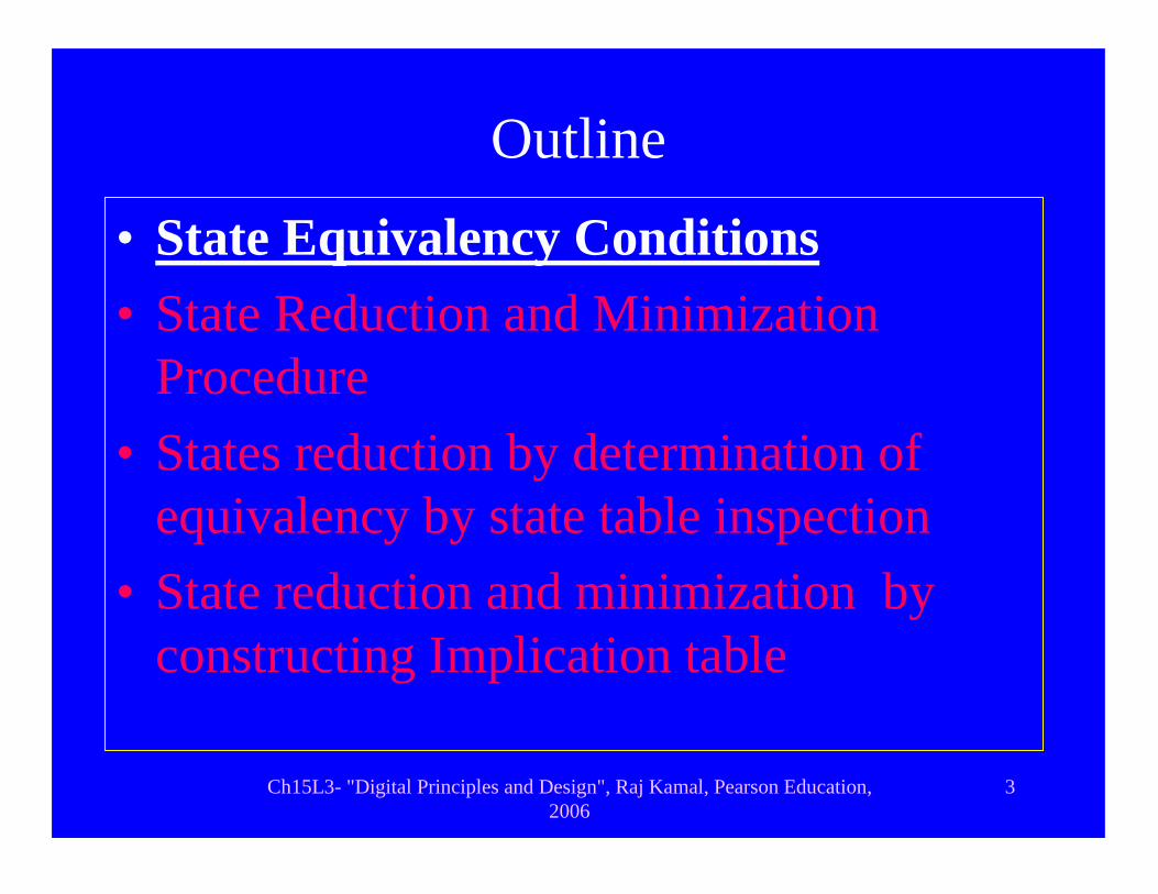
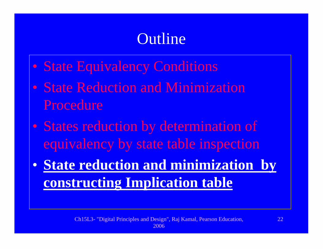
Outline
• State Equivalency Conditions• State Reduction and Minimization
Procedure• States reduction by determination of
equivalency by state table inspection • State reduction and minimization by
constructing Implication table
Ch15L3- "Digital Principles and Design", Raj Kamal, Pearson Education, 2006
4
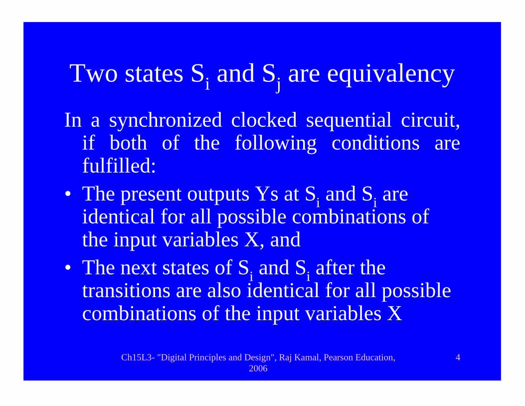
Two states Si and Sj are equivalency
In a synchronized clocked sequential circuit, if both of the following conditions are fulfilled:
• The present outputs Ys at Si and Si are identical for all possible combinations of the input variables X, and
• The next states of Si and Si after the transitions are also identical for all possible combinations of the input variables X
Ch15L3- "Digital Principles and Design", Raj Kamal, Pearson Education, 2006
5
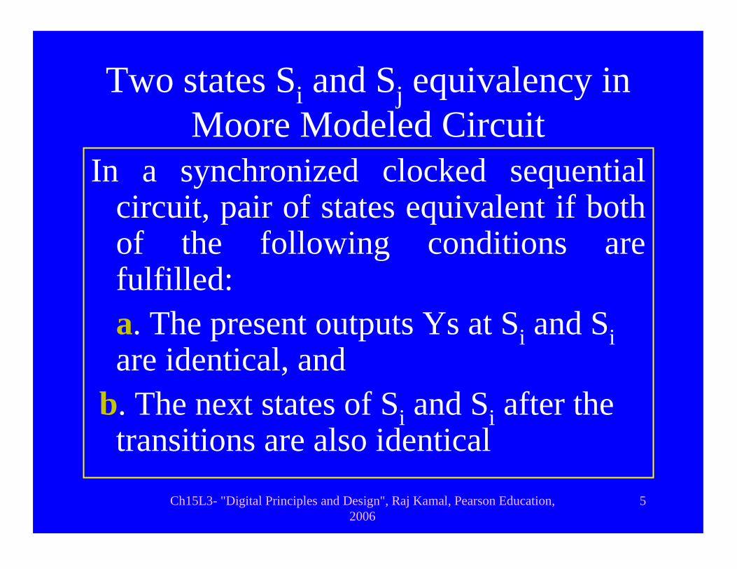
Two states Si and Sj equivalency in Moore Modeled Circuit
In a synchronized clocked sequential circuit, pair of states equivalent if both of the following conditions are fulfilled:a. The present outputs Ys at Si and Siare identical, and
b. The next states of Si and Si after the transitions are also identical
Ch15L3- "Digital Principles and Design", Raj Kamal, Pearson Education, 2006
6
Equivalent sequential circuits
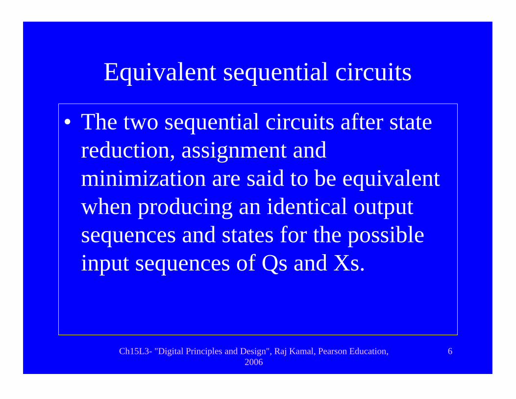
• The two sequential circuits after state reduction, assignment and minimization are said to be equivalent when producing an identical output sequences and states for the possible input sequences of Qs and Xs.
Ch15L3- "Digital Principles and Design", Raj Kamal, Pearson Education, 2006
7
Outline
• State Equivalency Conditions• State Reduction and Minimization
Procedure• States reduction by determination of
equivalency by state table inspection • State reduction and minimization by
constructing Implication table
Ch15L3- "Digital Principles and Design", Raj Kamal, Pearson Education, 2006
8
State Reduction
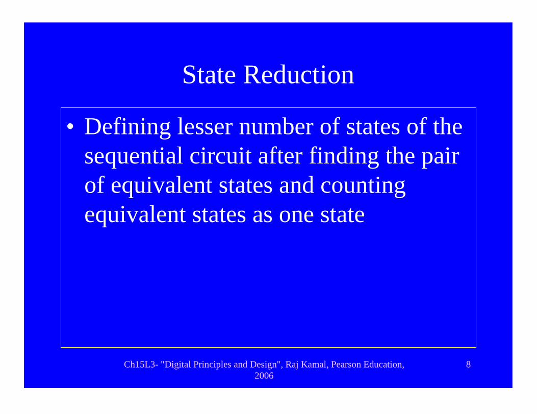
• Defining lesser number of states of the sequential circuit after finding the pair of equivalent states and counting equivalent states as one state
Ch15L3- "Digital Principles and Design", Raj Kamal, Pearson Education, 2006
9
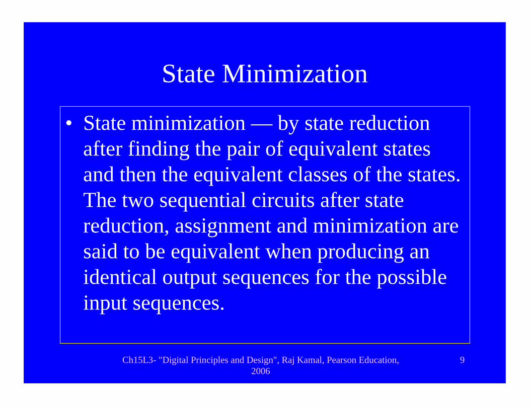
State Minimization
• State minimization — by state reduction after finding the pair of equivalent states and then the equivalent classes of the states. The two sequential circuits after state reduction, assignment and minimization are said to be equivalent when producing an identical output sequences for the possible input sequences.
Ch15L3- "Digital Principles and Design", Raj Kamal, Pearson Education, 2006
10
Outline
• State Equivalency Conditions• State Reduction and Minimization
Procedure• States reduction by determination of
equivalency by state table inspection • State reduction and minimization by
constructing Implication table
Ch15L3- "Digital Principles and Design", Raj Kamal, Pearson Education, 2006
11
State table inspection
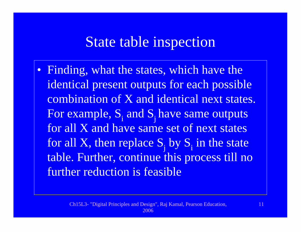
• Finding, what the states, which have the identical present outputs for each possible combination of X and identical next states. For example, Si and Sj have same outputs for all X and have same set of next states for all X, then replace Sj by Si in the state table. Further, continue this process till no further reduction is feasible
Ch15L3- "Digital Principles and Design", Raj Kamal, Pearson Education, 2006
12
State Names
• Let (Q0, Q1, Q2) = 000 S1• Let (Q0, Q1, Q2) = 001 S2 • .• .• Let (Q0, Q1, Q2) = 110 S7 • Let (Q0, Q1, Q2) = 111 S8
Ch15L3- "Digital Principles and Design", Raj Kamal, Pearson Education, 2006
13
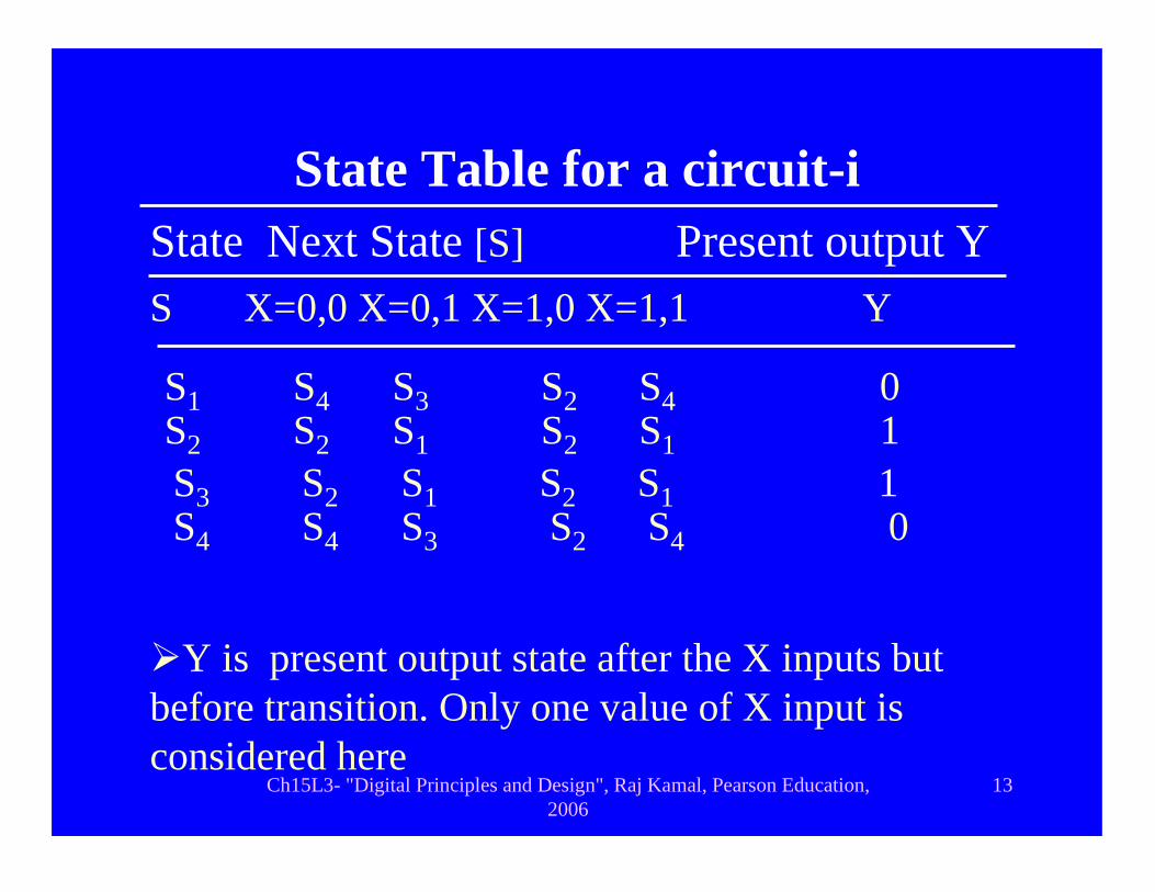
State Table for a circuit-iState Next State [S] Present output Y S X=0,0 X=0,1 X=1,0 X=1,1 Y
�Y is present output state after the X inputs but before transition. Only one value of X input is considered here
S1 S4 S3 S2 S4 0S2 S2 S1 S2 S1 1S3 S2 S1 S2 S1 1S4 S4 S3 S2 S4 0

Ch15L3- "Digital Principles and Design", Raj Kamal, Pearson Education, 2006
14
State Table for a circuit-iState Next State [S] Present output Y S X=0,0 X=0,1 X=1,0 X=1,1 Y
�Y is present output state after the X inputs but before transition. Only one value of X input is considered here
S5 S4 S3 S2 S4 0S6 S2 S1 S2 S1 1S7 S3 S4 S3 S4 0S8 S1 S2 S1 S2 1
Ch15L3- "Digital Principles and Design", Raj Kamal, Pearson Education, 2006
15
State table inspection
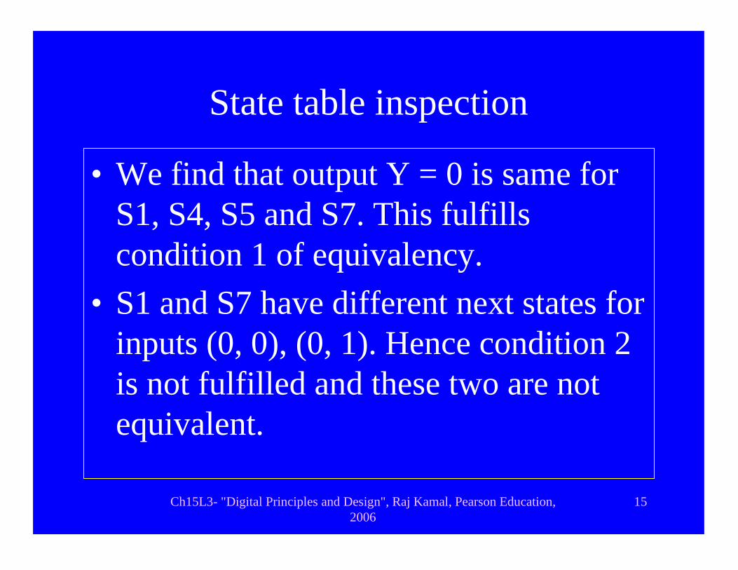
• We find that output Y = 0 is same for S1, S4, S5 and S7. This fulfills condition 1 of equivalency.
• S1 and S7 have different next states for inputs (0, 0), (0, 1). Hence condition 2 is not fulfilled and these two are not equivalent.
Ch15L3- "Digital Principles and Design", Raj Kamal, Pearson Education, 2006
16
State table inspection and reduction
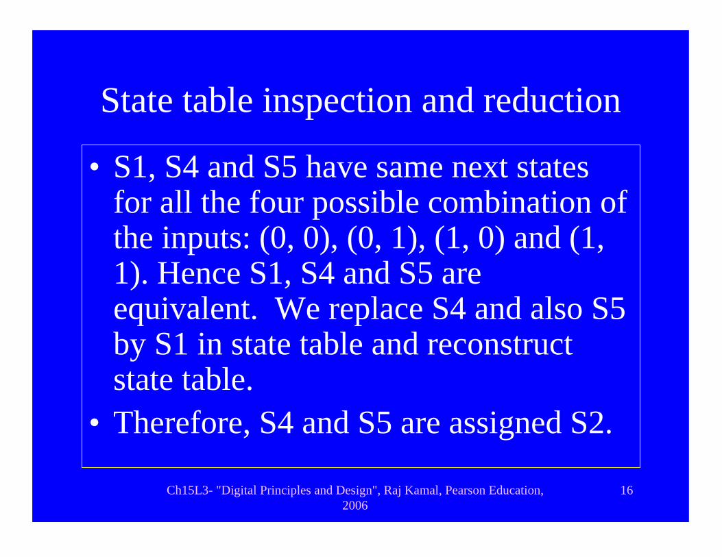
• S1, S4 and S5 have same next states for all the four possible combination of the inputs: (0, 0), (0, 1), (1, 0) and (1, 1). Hence S1, S4 and S5 are equivalent. We replace S4 and also S5 by S1 in state table and reconstruct state table.
• Therefore, S4 and S5 are assigned S2.
Ch15L3- "Digital Principles and Design", Raj Kamal, Pearson Education, 2006
17
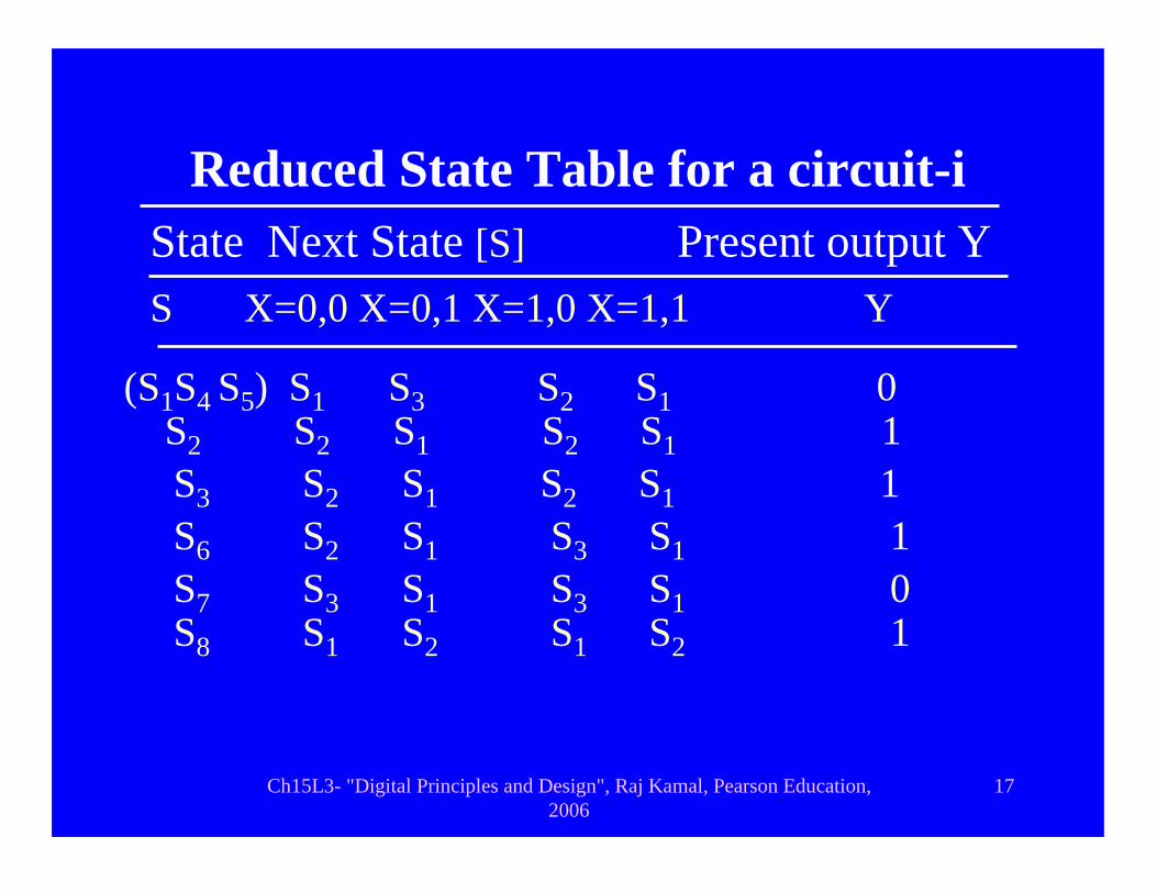
Reduced State Table for a circuit-iState Next State [S] Present output Y S X=0,0 X=0,1 X=1,0 X=1,1 Y
(S1S4 S5) S1 S3 S2 S1 0S2 S2 S1 S2 S1 1S3 S2 S1 S2 S1 1S6 S2 S1 S3 S1 1S7 S3 S1 S3 S1 0S8 S1 S2 S1 S2 1
Ch15L3- "Digital Principles and Design", Raj Kamal, Pearson Education, 2006
18
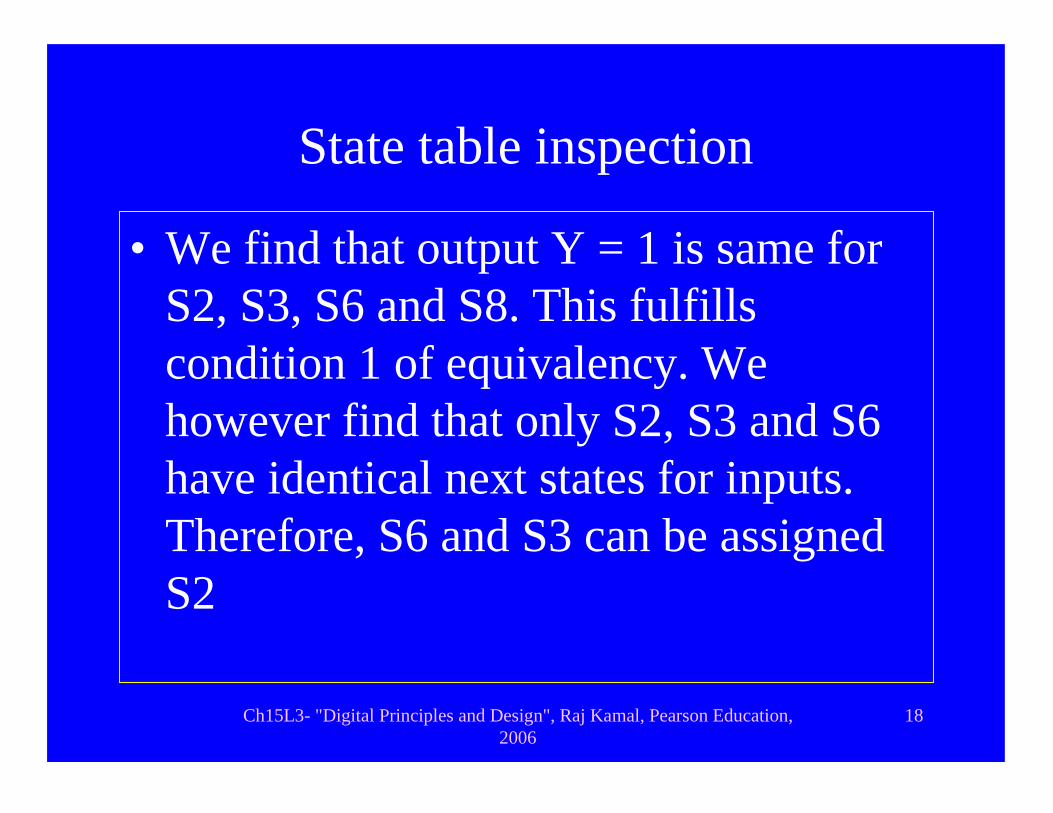
State table inspection
• We find that output Y = 1 is same for S2, S3, S6 and S8. This fulfills condition 1 of equivalency. We however find that only S2, S3 and S6 have identical next states for inputs. Therefore, S6 and S3 can be assigned S2
Ch15L3- "Digital Principles and Design", Raj Kamal, Pearson Education, 2006
19
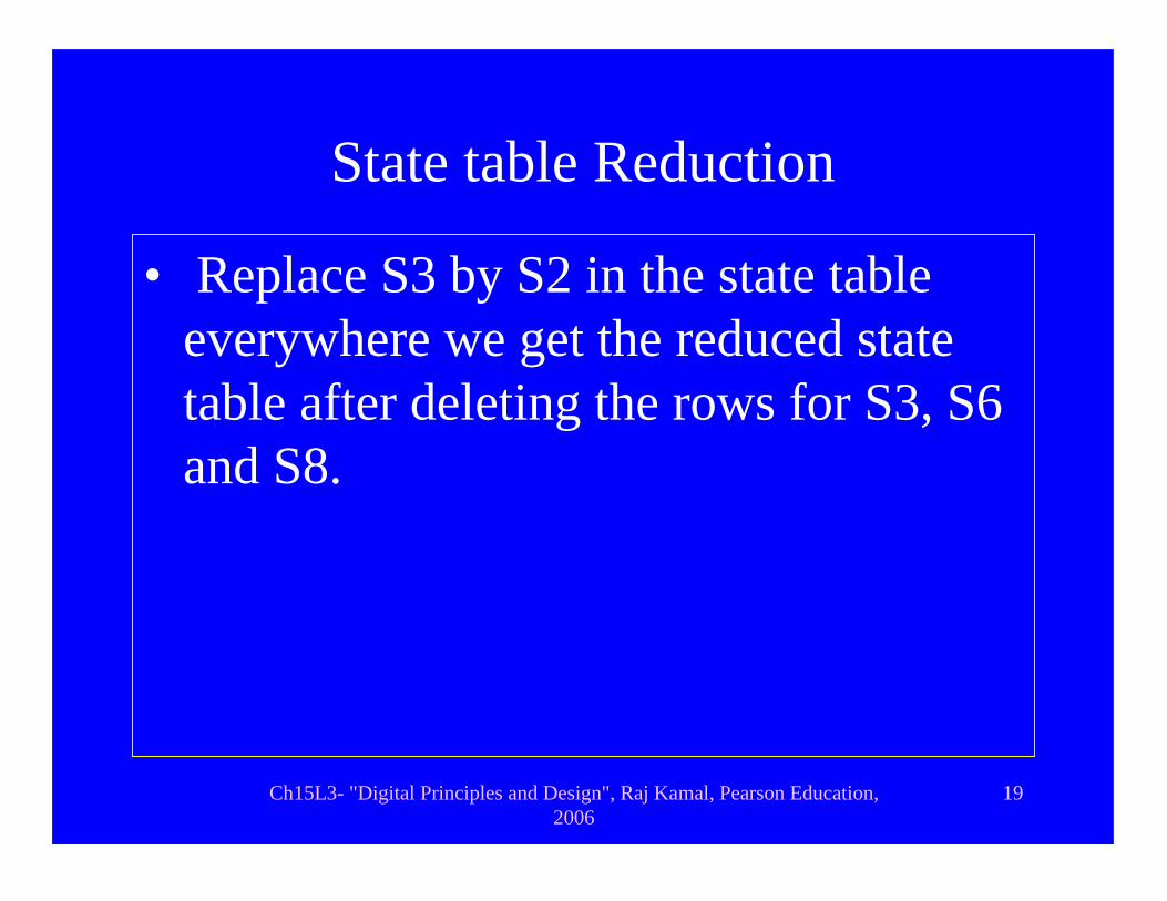
State table Reduction
• Replace S3 by S2 in the state table everywhere we get the reduced state table after deleting the rows for S3, S6 and S8.
Ch15L3- "Digital Principles and Design", Raj Kamal, Pearson Education, 2006
20
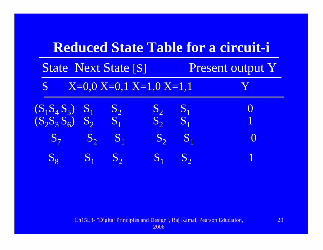
Reduced State Table for a circuit-iState Next State [S] Present output Y S X=0,0 X=0,1 X=1,0 X=1,1 Y
(S1S4 S5) S1 S2 S2 S1 0(S2S3 S6) S2 S1 S2 S1 1
S7 S2 S1 S2 S1 0
S8 S1 S2 S1 S2 1
Ch15L3- "Digital Principles and Design", Raj Kamal, Pearson Education, 2006
21
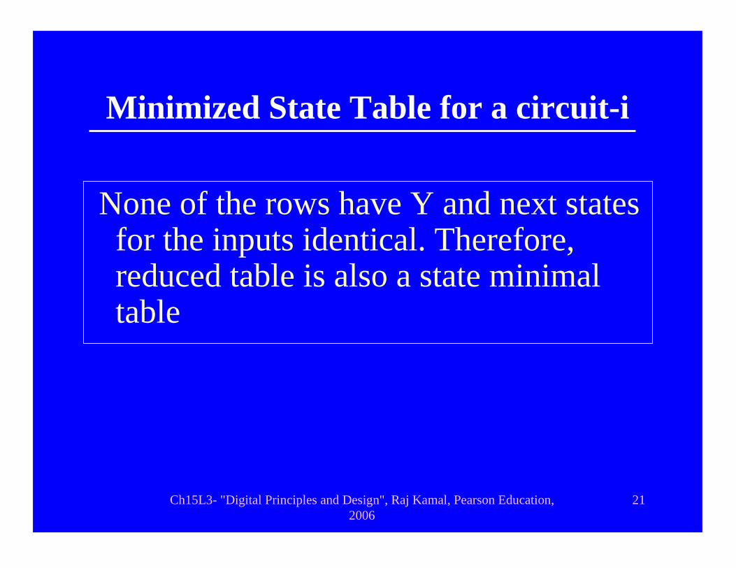
Minimized State Table for a circuit-i
None of the rows have Y and next states for the inputs identical. Therefore, reduced table is also a state minimal table
Ch15L3- "Digital Principles and Design", Raj Kamal, Pearson Education, 2006
22
Outline
• State Equivalency Conditions• State Reduction and Minimization
Procedure• States reduction by determination of
equivalency by state table inspection • State reduction and minimization by
constructing Implication table

Ch15L3- "Digital Principles and Design", Raj Kamal, Pearson Education, 2006
23
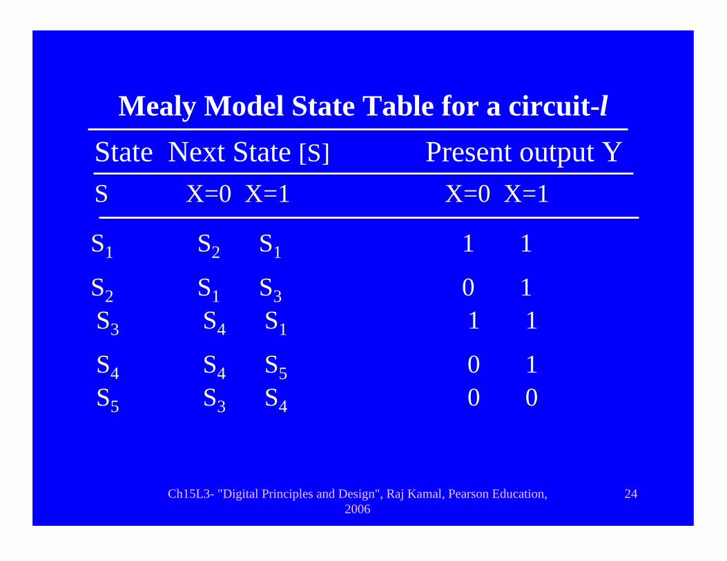
Constructing Implication Table
• Step 1: Construct a state table
Ch15L3- "Digital Principles and Design", Raj Kamal, Pearson Education, 2006
24
Mealy Model State Table for a circuit-lState Next State [S] Present output Y S X=0 X=1 X=0 X=1
S1 S2 S1 1 1
S2 S1 S3 0 1 S3 S4 S1 1 1
S4 S4 S5 0 1 S5 S3 S4 0 0
Ch15L3- "Digital Principles and Design", Raj Kamal, Pearson Education, 2006
25
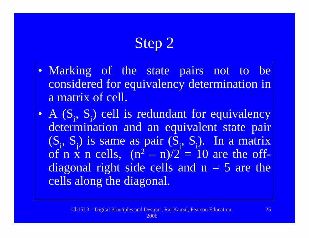
Step 2
• Marking of the state pairs not to be considered for equivalency determination in a matrix of cell.
• A (Si, Si) cell is redundant for equivalency determination and an equivalent state pair (Si, Sj) is same as pair (Sj, Si). In a matrix of n x n cells, (n2 – n)/2 = 10 are the off-diagonal right side cells and n = 5 are the cells along the diagonal.
Ch15L3- "Digital Principles and Design", Raj Kamal, Pearson Education, 2006
26
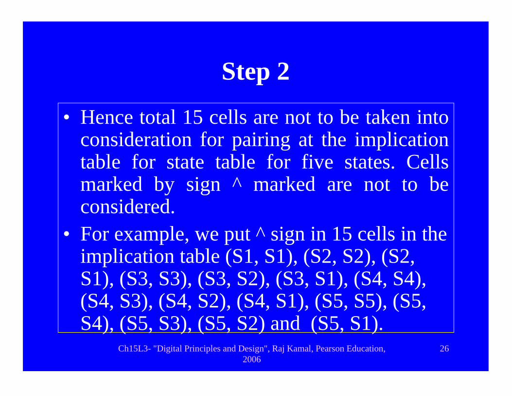
Step 2
• Hence total 15 cells are not to be taken into consideration for pairing at the implication table for state table for five states. Cells marked by sign ^ marked are not to be considered.
• For example, we put ^ sign in 15 cells in the implication table (S1, S1), (S2, S2), (S2, S1), (S3, S3), (S3, S2), (S3, S1), (S4, S4), (S4, S3), (S4, S2), (S4, S1), (S5, S5), (S5, S4), (S5, S3), (S5, S2) and (S5, S1).
Ch15L3- "Digital Principles and Design", Raj Kamal, Pearson Education, 2006
27
Step 3
• Put # sign for a cell not having the same set of output for all the input combinations
Ch15L3- "Digital Principles and Design", Raj Kamal, Pearson Education, 2006
28
Step 3 Circuit-l
• Put # sign for a cell not having the same set of output for all the input combinations
Ch15L3- "Digital Principles and Design", Raj Kamal, Pearson Education, 2006
29
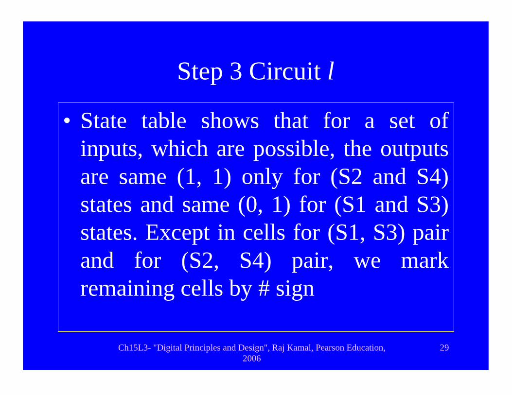
Step 3 Circuit l
• State table shows that for a set of inputs, which are possible, the outputs are same (1, 1) only for (S2 and S4) states and same (0, 1) for (S1 and S3) states. Except in cells for (S1, S3) pair and for (S2, S4) pair, we mark remaining cells by # sign
Ch15L3- "Digital Principles and Design", Raj Kamal, Pearson Education, 2006
30
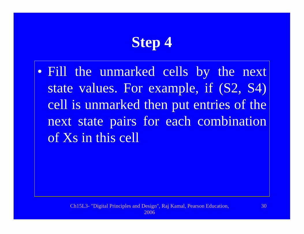
Step 4
• Fill the unmarked cells by the next state values. For example, if (S2, S4) cell is unmarked then put entries of the next state pairs for each combination of Xs in this cell
Ch15L3- "Digital Principles and Design", Raj Kamal, Pearson Education, 2006
31
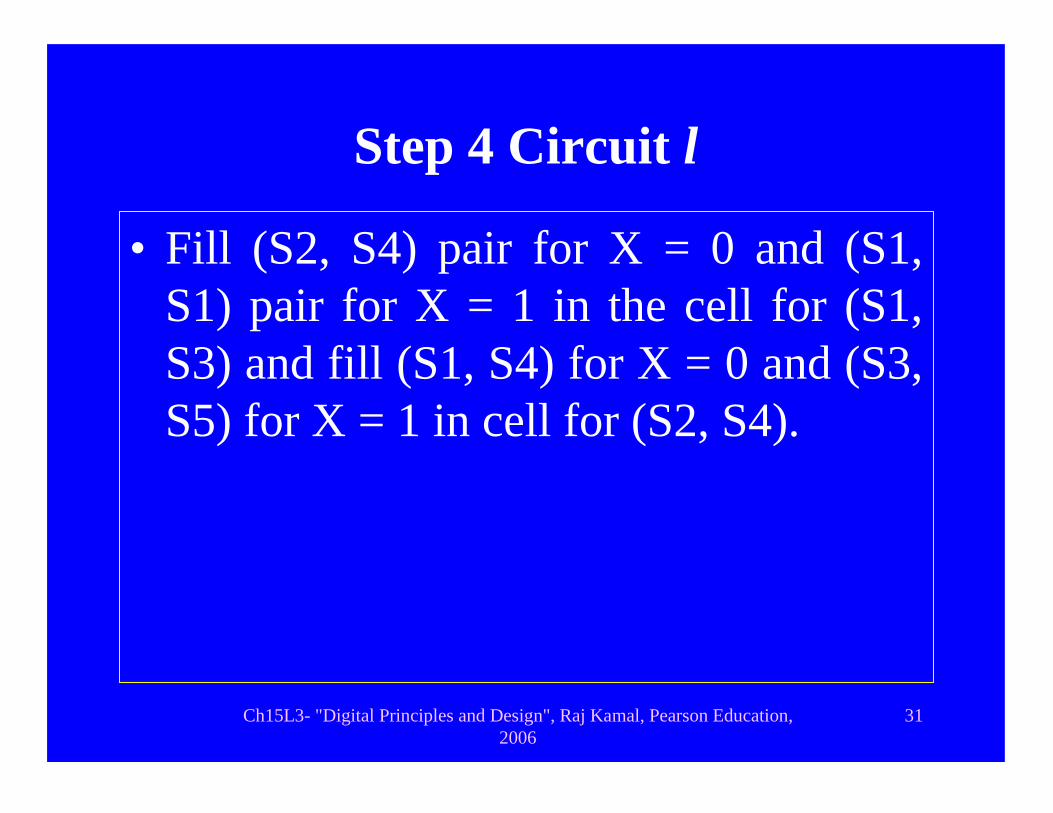
Step 4 Circuit l
• Fill (S2, S4) pair for X = 0 and (S1, S1) pair for X = 1 in the cell for (S1, S3) and fill (S1, S4) for X = 0 and (S3, S5) for X = 1 in cell for (S2, S4).
Ch15L3- "Digital Principles and Design", Raj Kamal, Pearson Education, 2006
32
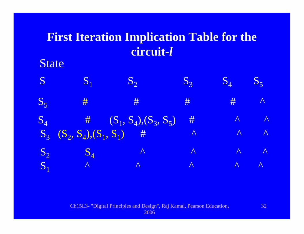
First Iteration Implication Table for the circuit-l
StateS S1 S2 S3 S4 S5
S5 # # # # ^
S4 # (S1, S4),(S3, S5) # ^ ^S3 (S2, S4),(S1, S1) # ^ ^ ^
S2 S4 ^ ^ ^ ^ S1 ^ ^ ^ ^ ^
Ch15L3- "Digital Principles and Design", Raj Kamal, Pearson Education, 2006
33
Step 5
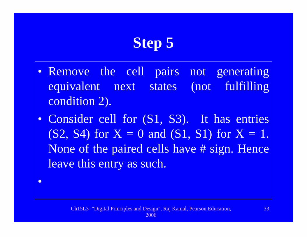
• Remove the cell pairs not generating equivalent next states (not fulfilling condition 2).
• Consider cell for (S1, S3). It has entries (S2, S4) for X = 0 and (S1, S1) for X = 1. None of the paired cells have # sign. Hence leave this entry as such.
•
Ch15L3- "Digital Principles and Design", Raj Kamal, Pearson Education, 2006
34
Step 5 circuit l
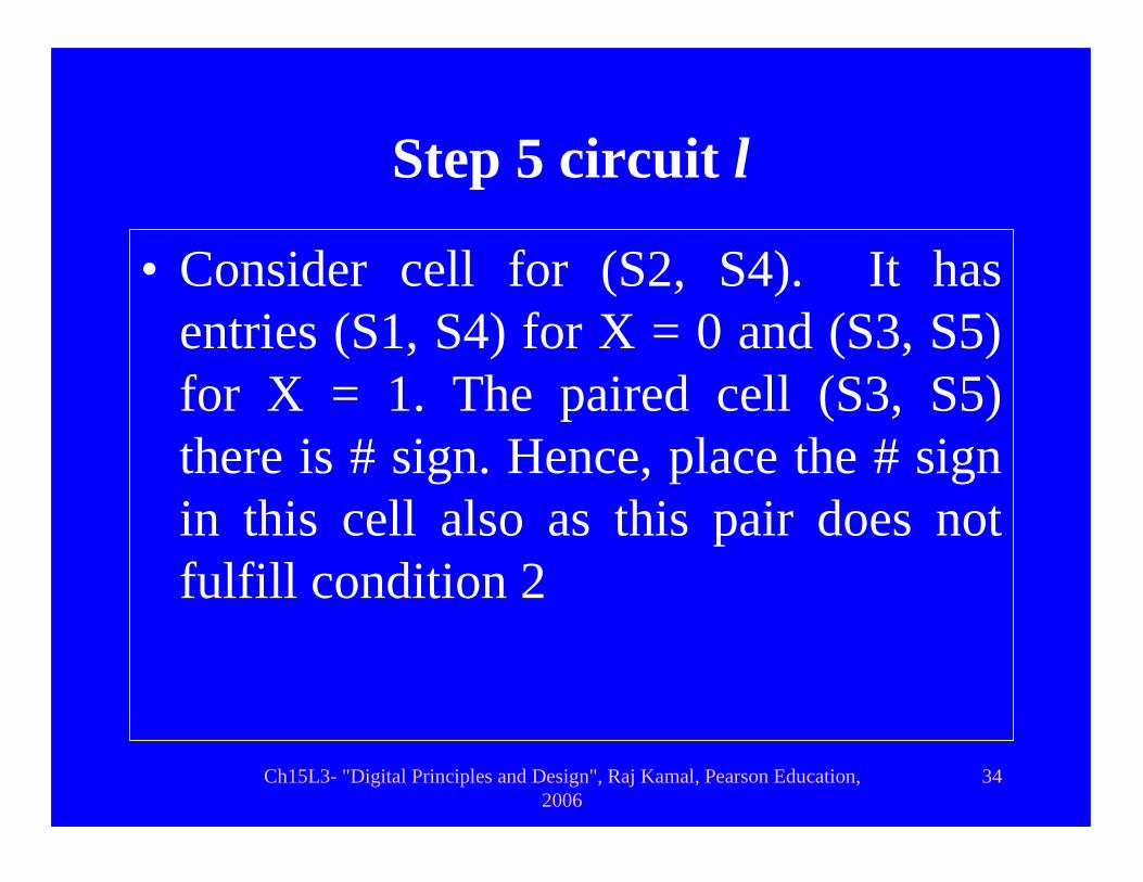
• Consider cell for (S2, S4). It has entries (S1, S4) for X = 0 and (S3, S5) for X = 1. The paired cell (S3, S5) there is # sign. Hence, place the # sign in this cell also as this pair does not fulfill condition 2
Ch15L3- "Digital Principles and Design", Raj Kamal, Pearson Education, 2006
35
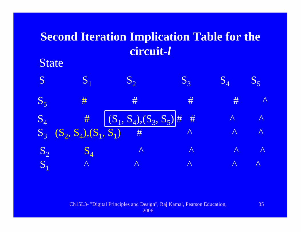
Second Iteration Implication Table for the circuit-l
StateS S1 S2 S3 S4 S5
S5 # # # # ^
S4 # (S1, S4),(S3, S5) # # ^ ^S3 (S2, S4),(S1, S1) # ^ ^ ^
S2 S4 ^ ^ ^ ^ S1 ^ ^ ^ ^ ^
Ch15L3- "Digital Principles and Design", Raj Kamal, Pearson Education, 2006
36
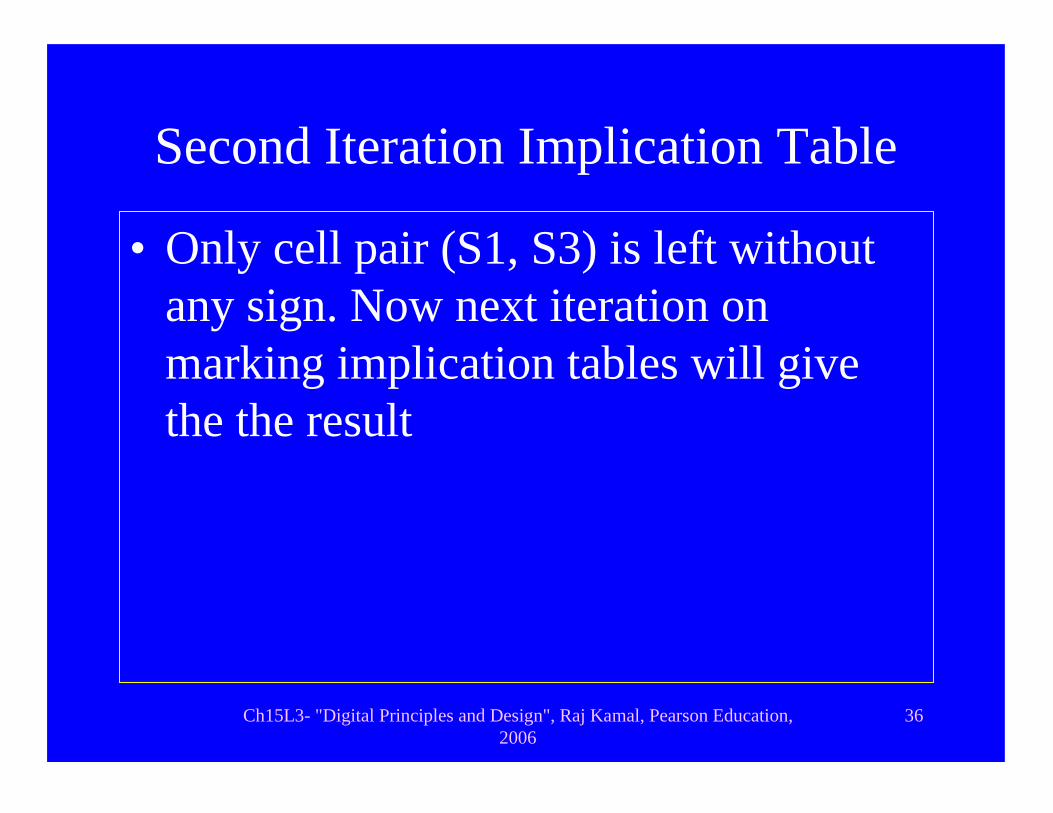
Second Iteration Implication Table
• Only cell pair (S1, S3) is left without any sign. Now next iteration on marking implication tables will give the the result

Ch15L3- "Digital Principles and Design", Raj Kamal, Pearson Education, 2006
37
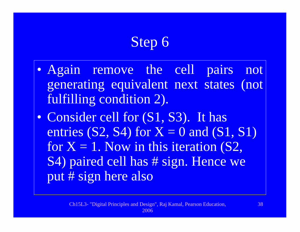
Step 6
• Step 6: Continue process in Step 5 till no more # sign needs to be placed. All the cells not generating equivalent next states (not fulfilling condition 2) are now free from # sign
Ch15L3- "Digital Principles and Design", Raj Kamal, Pearson Education, 2006
38
Step 6
• Again remove the cell pairs not generating equivalent next states (not fulfilling condition 2).
• Consider cell for (S1, S3). It has entries (S2, S4) for X = 0 and (S1, S1) for X = 1. Now in this iteration (S2, S4) paired cell has # sign. Hence we put # sign here also
Ch15L3- "Digital Principles and Design", Raj Kamal, Pearson Education, 2006
39
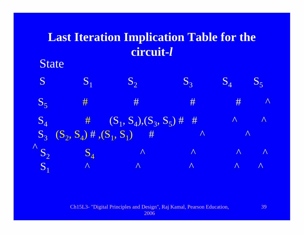
Last Iteration Implication Table for the circuit-l
StateS S1 S2 S3 S4 S5
S5 # # # # ^
S4 # (S1, S4),(S3, S5) # # ^ ^S3 (S2, S4) # ,(S1, S1) # ^ ^
^ S2 S4 ^ ^ ^ ^ S1 ^ ^ ^ ^ ^
Ch15L3- "Digital Principles and Design", Raj Kamal, Pearson Education, 2006
40
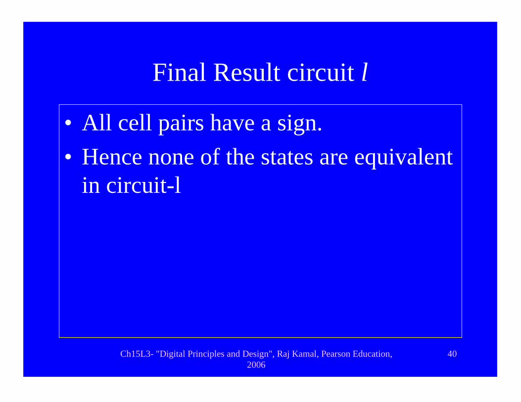
Final Result circuit l
• All cell pairs have a sign.• Hence none of the states are equivalent
in circuit-l
Summary
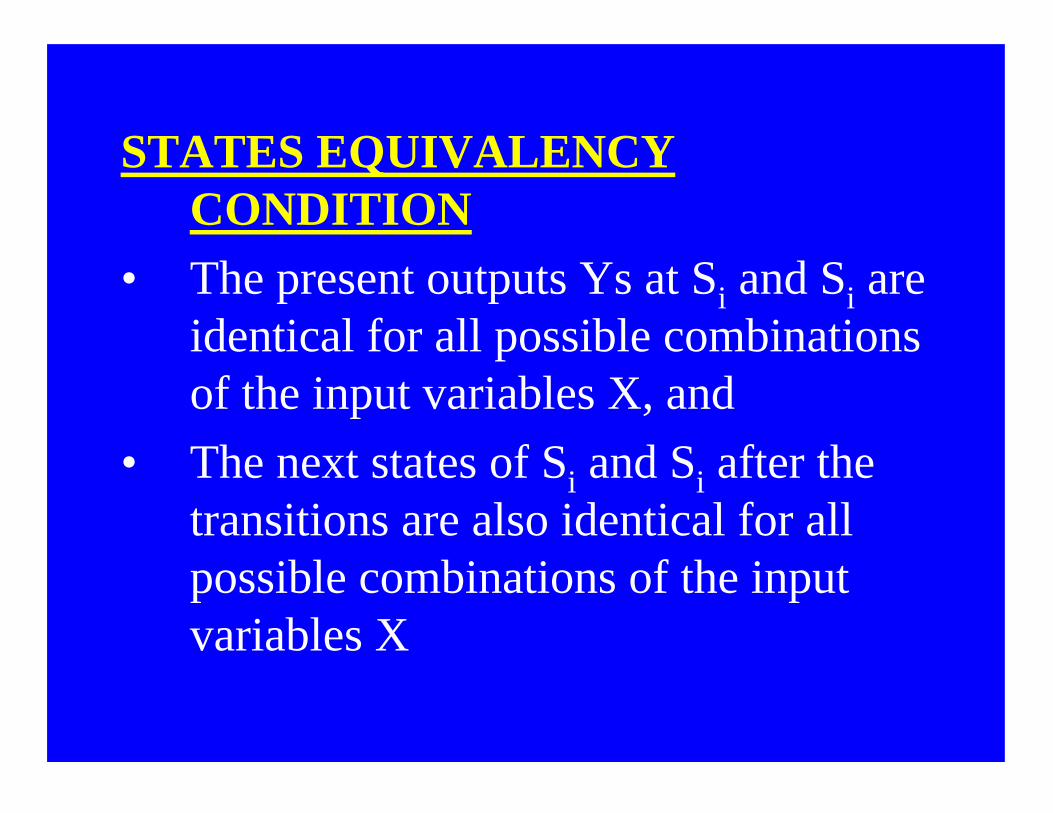
STATES EQUIVALENCY CONDITION
• The present outputs Ys at Si and Si are identical for all possible combinations of the input variables X, and
• The next states of Si and Si after the transitions are also identical for all possible combinations of the input variables X
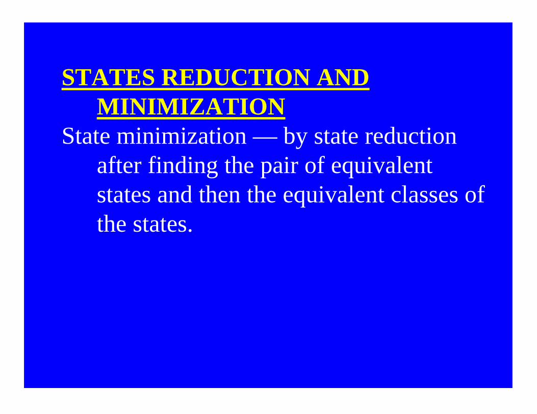
STATES REDUCTION AND MINIMIZATION
State minimization — by state reduction after finding the pair of equivalent states and then the equivalent classes of the states.
End of Lesson 3 on States equivalency,
state reduction and state minimization

Ch15L3- "Digital Principles and Design", Raj Kamal, Pearson Education, 2006
45
THANK YOU