Assembly of Mechanically Compliant Interfaces between ... · IEEE 64 th ECTC – Orlando, FL, USA...
14
IEEE 64 th ECTC – Orlando, FL, USA May 27–30, 2014 Add Company Logo Here Assembly of Mechanically Compliant Interfaces between Optical Fibers and Nanophotonic Chips T. Barwicz, Y. Taira , H. Numata, N. Boyer, S. Harel, S. Kamlapurkar, S. Takenobu, S. Laflamme, S. Engelmann, Y. Vlasov, and P. Fortier
Transcript of Assembly of Mechanically Compliant Interfaces between ... · IEEE 64 th ECTC – Orlando, FL, USA...

IEEE 64th ECTC – Orlando, FL, USA May 27–30, 2014
Add Company
Logo Here
Assembly of Mechanically Compliant Interfaces between Optical Fibers and Nanophotonic Chips
T. Barwicz, Y. Taira, H. Numata, N. Boyer, S.
Harel, S. Kamlapurkar, S. Takenobu, S. Laflamme,
S. Engelmann, Y. Vlasov, and P. Fortier
2IEEE 64th ECTC – Orlando, FL, USA May 27 – 30, 2014T. Barwicz, T. Taira, et al. 2May 27 – 30, 2014
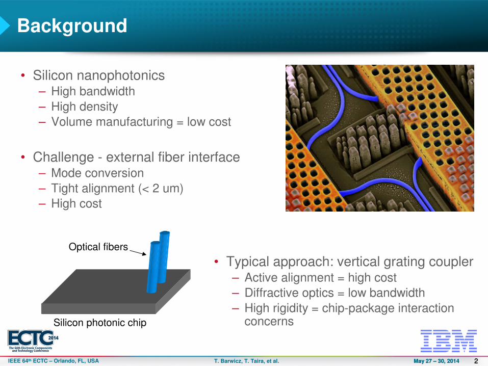
Background
• Silicon nanophotonics– High bandwidth
– High density
– Volume manufacturing = low cost
• Challenge - external fiber interface– Mode conversion
– Tight alignment (< 2 um)
– High cost
• Typical approach: vertical grating coupler– Active alignment = high cost
– Diffractive optics = low bandwidth
– High rigidity = chip-package interaction concernsSilicon photonic chip
Optical fibers

3IEEE 64th ECTC – Orlando, FL, USA May 27 – 30, 2014T. Barwicz, T. Taira, et al. 3May 27 – 30, 2014
Compliant interface: concept
Nanophotonic die
Mechanically compliant extension with
integrated polymer waveguides
Standard fiber
interface
Adiabatic optical
coupling
• Standard self-aligned fiber interface
• Integrated, flexible polymer waveguides
• High-speed, self-aligned assembly to chip
4IEEE 64th ECTC – Orlando, FL, USA May 27 – 30, 2014T. Barwicz, T. Taira, et al. 4May 27 – 30, 2014
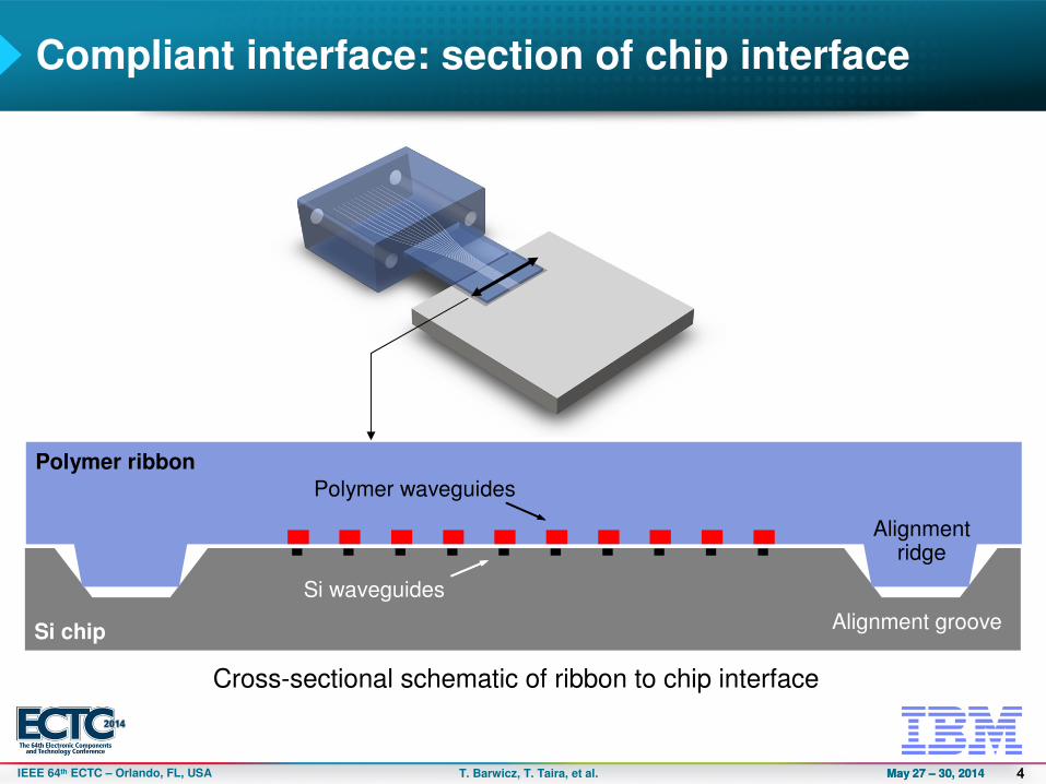
Compliant interface: section of chip interface
Si chip
Polymer ribbon
Si waveguides
Polymer waveguides
Alignment groove
Alignment ridge
Cross-sectional schematic of ribbon to chip interface

5IEEE 64th ECTC – Orlando, FL, USA May 27 – 30, 2014T. Barwicz, T. Taira, et al. 5May 27 – 30, 2014
Lithographically defined polymer waveguides assembled to a molded ferrule
Compliant interface: implementation here
Mechanically
compliant extension
Standard fiber
interface
Nanophotonic
die
Ferrule lid
Polymer ribbon
with waveguides
Ferrule for interfacing
to fibers
Die with
nanophotonic circuits
Coupling region

6IEEE 64th ECTC – Orlando, FL, USA May 27 – 30, 2014T. Barwicz, T. Taira, et al. 6May 27 – 30, 2014
Compliant interface: flex to ferrule assembly
Ferrule
Polymer
ribbon
Ferrule
lid
Polymer ribbon
MT pin
hole
- Dispense adhesive
- Place ribbon in ferrule
- Apply pressure
- UV cure adhesive
- Place lid
- Cure lid adhesive
- Angle polish fiber
interface
• MT based parallel fiber interface
• Self-alignment structures for high-speed machine assembly

7IEEE 64th ECTC – Orlando, FL, USA May 27 – 30, 2014T. Barwicz, T. Taira, et al. 7May 27 – 30, 2014
Accurate fabrication + self-aligned assembly = 1-2 um placement accuracy
Compliant interface: flex to ferrule accuracy
101.1 µm
(100 +/-2 µm)
20.5 µm
(20 +1/-3 µm)
250.0 µm
(250 µm)
200.8 µm
(200 µm)
101.1 µm
(100+/-2 µm)
250.0 µm
(250 µm)
199.5 µm
(200 µm)
Ferrule
Ferrule lid
Polymer ribbon backing
Polymer waveguides Self-
alignment
structure
8IEEE 64th ECTC – Orlando, FL, USA May 27 – 30, 2014T. Barwicz, T. Taira, et al. 8May 27 – 30, 2014
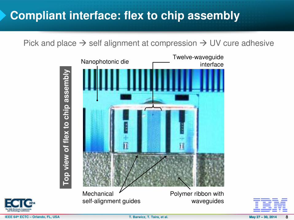
Pick and place � self alignment at compression � UV cure adhesive
Compliant interface: flex to chip assembly
Polymer ribbon with
waveguides
Twelve-waveguide
interface
Mechanical
self-alignment guides
Nanophotonic dieT
op
vie
w o
f fl
ex t
o c
hip
assem
bly
9IEEE 64th ECTC – Orlando, FL, USA May 27 – 30, 2014T. Barwicz, T. Taira, et al. 9May 27 – 30, 2014
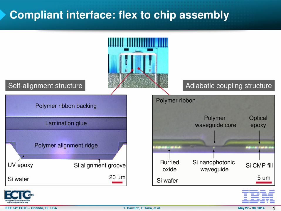
Compliant interface: flex to chip assembly
Si alignment groove
Polymer alignment ridge
Polymer ribbon backing
Lamination glue
Si wafer 20 um
UV epoxy
Si wafer
Polymer ribbon
Polymer
waveguide core
Si nanophotonic
waveguideSi CMP fill
Optical
epoxy
5 um
Burried
oxide
Self-alignment structure Adiabatic coupling structure

10IEEE 64th ECTC – Orlando, FL, USA May 27 – 30, 2014T. Barwicz, T. Taira, et al. 10May 27 – 30, 2014
Compliant interface: alignment accuracy readout
Edges of polymer
waveguide
Si nanophotonic
waveguide
Si CMP fill
4 um
Alignment
readout marks
Measure polymer waveguide to nanophotonic waveguide alignment:� cross-sections and alignment accuracy readout structures

11IEEE 64th ECTC – Orlando, FL, USA May 27 – 30, 2014T. Barwicz, T. Taira, et al. 11May 27 – 30, 2014
Compliant interface: self-alignment performance
Starting misalignment: -10 to +10 umResulting misalignment: ~1 um (typical), < 2 um (always)
-10 -5 0 5 10-8
-6
-4
-2
0
2
4
6
Purposefully induced misalignment (um)
Re
su
ltin
g m
isa
lignm
en
t (u
m)
Brut data
top left
top right
bottom left
bottom right
All assemblies in allowed range
Measurement positions circled
8

12IEEE 64th ECTC – Orlando, FL, USA May 27 – 30, 2014T. Barwicz, T. Taira, et al. 12May 27 – 30, 2014
top lefttop rightbottom leftbottom right
Compliant interface: self-alignment angle
Decomposing residual misalignment into angular and lateral components� see correlation between initial and final lateral misalignment
An
gle
(de
gre
e)
-0.05
-0.04
-0.03
-0.02
-0.01
0.01
0.02
-10 -5 0 5 10
0
Angle of rotation
Purposefully induced misalignment (um)-10 -5 0 5 10
-2
-1.5
-1
-0.5
0
0.5
1
1.5
2
Purposefully induced misalignment (um)
Re
su
ltin
g m
isa
lignm
en
t (u
m)
Misalignment after subtraction of rotation
Correlation via deformation
of polymer alignment ridge
Structure inaccuracy

13IEEE 64th ECTC – Orlando, FL, USA May 27 – 30, 2014T. Barwicz, T. Taira, et al. 13May 27 – 30, 2014
Conclusion
• What has been achieved:– Self-aligned assembly of ribbon to ferrule
– Self-aligned assembly to silicon photonic chip
• Demonstrated feasibility of single-mode optics assembly in high speed microelectronics tools
• Single-mode optics requires < 2 um alignment
• Demonstrated self-alignment to 1-2 um from +/- 10 um purposeful misalignment
• Limit of re-alignment set by structure accuracy
– +/- 0.5 um for ribbon to Si alignment
– +/- 1.5 um for ribbon to ferrule alignment
14IEEE 64th ECTC – Orlando, FL, USA May 27 – 30, 2014T. Barwicz, T. Taira, et al. 14May 27 – 30, 2014
Team and acknowledgments
IBM Watson, NY USAInterface design, Si fabrication
IBM Research - TokyoRibbon to ferrule assembly
IBM Bromont – C2MIRibbon to Si assembly
Outside partners
Shotaro TakenobuPolymer waveguide fabrication
Masato ShiinoFerrule fabrication
Supported by