
ASNT611 9 ASNT6119B-KMF 33.5Gbps Advanced · PDF file · 2017-09-22Functional Block...
15
Rev.1.1.1 September 2017 1 Advanced Science And Novel Technology Company, Inc. 27 Via Porto Grande, Rancho Palos Verdes, CA 90275 Offices: 310-377-6029 / 310-803-9284 Fax: 310-377-9940 www.adsantec.com ASNT6119B-KMF 33.5Gbps Advanced Driver/Amplifier High-speed limiting amplifier with selectable built-in pre-emphasis Four pre-emphasis taps with externally controlled weight and inversion Adjustable data output amplitude and eye quality Single-ended output data eye cross point adjustment Optional main clock frequency multiplier by 2 Main clock duty cycle indicators located before and after the multiplier Opposite and parallel adjustment of the main clock and data delays Additional clock input Fully differential CML input and output data, and clock interfaces Selectable main or additional clock at the output with adjustable amplitude Standard CMOS 3-wire interface for digital controls On-chip linear temperature sensor Two power supplies: negative -4.3V and floating positive +3.5V Average power consumption: 4.0W Custom CQFP 64-pin package tune1 tune2 tune3 tune4 vth ASNT6119 ASNT6119B
-
Upload
nguyendiep -
Category
Documents
-
view
215 -
download
2
Transcript of ASNT611 9 ASNT6119B-KMF 33.5Gbps Advanced · PDF file · 2017-09-22Functional Block...

Rev.1.1.1 September 2017 1
Advanced Science And Novel Technology Company, Inc.
27 Via Porto Grande, Rancho Palos Verdes, CA 90275
Offices: 310-377-6029 / 310-803-9284 Fax: 310-377-9940
www.adsantec.com
ASNT6119B-KMF
33.5Gbps Advanced Driver/Amplifier
High-speed limiting amplifier with selectable built-in pre-emphasis
Four pre-emphasis taps with externally controlled weight and inversion
Adjustable data output amplitude and eye quality
Single-ended output data eye cross point adjustment
Optional main clock frequency multiplier by 2
Main clock duty cycle indicators located before and after the multiplier
Opposite and parallel adjustment of the main clock and data delays
Additional clock input
Fully differential CML input and output data, and clock interfaces
Selectable main or additional clock at the output with adjustable amplitude
Standard CMOS 3-wire interface for digital controls
On-chip linear temperature sensor
Two power supplies: negative -4.3V and floating positive +3.5V
Average power consumption: 4.0W
Custom CQFP 64-pin package
tun
e1
tun
e2
tun
e3
tun
e4
vth
ASNT6119
ASNT6119B
Rev.1.1.1 September 2017 2
Advanced Science And Novel Technology Company, Inc.
27 Via Porto Grande, Rancho Palos Verdes, CA 90275
Offices: 310-377-6029 / 310-803-9284 Fax: 310-377-9940
www.adsantec.com
DESCRIPTION
xadjp/xadjn dp/dn
ci0p/ci0n
skwadj
Delay2
dlyadj
Clk x2
phadj
DCycl
ci1p/ci1n
SB
I
g
I
I
I
tune1/2/3/4
DOB qp/qn
vddshd
temp
dcyc0
3wdin
3wcin
3wenin
T1
T2
T4
T3
vth
Delay2
Delay1
Delay1
COB cop/con
vddshc
campadj
DCycl dcyc1
dcqp/dcqn
Temp
cose
l
inv
1/2
/3/4
dlypol skwpol
3-Wire Interface
Dig
ital
tap
co
ntr
ols
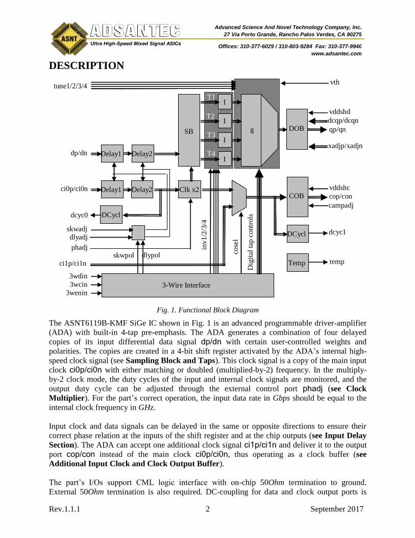
Fig. 1. Functional Block Diagram
The ASNT6119B-KMF SiGe IC shown in Fig. 1 is an advanced programmable driver-amplifier
(ADA) with built-in 4-tap pre-emphasis. The ADA generates a combination of four delayed
copies of its input differential data signal dp/dn with certain user-controlled weights and
polarities. The copies are created in a 4-bit shift register activated by the ADA’s internal high-
speed clock signal (see Sampling Block and Taps). This clock signal is a copy of the main input
clock ci0p/ci0n with either matching or doubled (multiplied-by-2) frequency. In the multiply-
by-2 clock mode, the duty cycles of the input and internal clock signals are monitored, and the
output duty cycle can be adjusted through the external control port phadj (see Clock
Multiplier). For the part’s correct operation, the input data rate in Gbps should be equal to the
internal clock frequency in GHz.
Input clock and data signals can be delayed in the same or opposite directions to ensure their
correct phase relation at the inputs of the shift register and at the chip outputs (see Input Delay
Section). The ADA can accept one additional clock signal ci1p/ci1n and deliver it to the output
port cop/con instead of the main clock ci0p/ci0n, thus operating as a clock buffer (see
Additional Input Clock and Clock Output Buffer).
The part’s I/Os support CML logic interface with on-chip 50Ohm termination to ground.
External 50Ohm termination is also required. DC-coupling for data and clock output ports is
Rev.1.1.1 September 2017 3
Advanced Science And Novel Technology Company, Inc.
27 Via Porto Grande, Rancho Palos Verdes, CA 90275
Offices: 310-377-6029 / 310-803-9284 Fax: 310-377-9940
www.adsantec.com
strongly recommended. The input ports can use DC or AC coupling. Differential input clock and
data are strongly recommended. Amplitude and peaking in the clock and data output signals can
be externally adjusted. Both single-ended data output signals also have controlled DC common-
mode levels and eye crossing points (see Data Output Buffer).
All operational modes of the chip are controlled through a 3-wire serial interface. For more
details see 3-Wire Interface Control Block.
The chip operates from one negative power supply (positive pin connected to external Ground,
negative pin vee = -4.3V) and one floating positive power supply (negative pin connected to vee
and positive pin v3p5 = 3.5V). It is recommended to keep the relative deviation of v3p5 from
Ground within less than ±0.1V.
Input Delay Section As shown in Fig. 1, the ADA accepts differential input data dp/dn and clock ci0p/ci0n signals
and inserts them both into identical variable delay blocks Delay1 and Delay2 that can be
adjusted in parallel or opposite modes depending on the polarity of internal digital signals
skwpol and dlypol (“0”=parallel, “1”=opposite) provided by the 3-Wire Interface block. The
Delay1 blocks are controlled by the analog voltage skwadj. The Delay2 blocks are controlled
by the analog voltage dlyadj.
It should be noted that the delay settings may affect the multiplied-by-2 clock’s duty cycle and
should be tuned for each specific case.
Clock Multiplier The clock doubler Clkx2 uses a “delay and XOR” mechanism to create output clock pulses from
each edge of the input clock ci0p/ci0n. The multiplier is intended for operation with input clock
signals within a certain frequency range specified in ELECTRICAL CHARACTERISTICS.
Analog control voltage phadj performs a dual function of multiplier activation and linear phase
control. Voltages within the linear control range activate the multiplication function and are used
for tuning the block’s internal delay in order to achieve 50% duty cycle of the multiplied clock.
Voltages below the switch-off threshold disable the multiplication function and allow for direct
passing of the input clock to the multiplier’s output.
Two duty cycle control blocks DCycl are used for monitoring the clock pulse shapes before and
after the multiplier. The first block is positioned before the multiplier and delivers single-ended
analog voltage dcyc0 that indicates the input clock’s duty cycle deviation from 50%. The second
block is positioned after the multiplier and delivers a similar signal dcyc1 for the output clock.
Both generated output voltages can be used in combination with phadj input within external
control loops for getting an optimal shape of the multiplied clock.
It should be noted that the duty cycle of the multiplied clock may depend on the delay settings
(see Input Delay Section).
Additional Input Clock and Clock Output Buffer The ADA can also accept an additional input clock signal ci1p/ci1n and deliver it to the clock
output. This allows the IC to operate solely as a clock amplifier where the output clock signal’s
Rev.1.1.1 September 2017 4
Advanced Science And Novel Technology Company, Inc.
27 Via Porto Grande, Rancho Palos Verdes, CA 90275
Offices: 310-377-6029 / 310-803-9284 Fax: 310-377-9940
www.adsantec.com
amplitude supplied by output buffer COB can be adjusted using the analog signal campadj. The
amplitude changes from its minimum value (campadj = switch-off threshold) to its maximum
value (campadj = maximum). COB can also be completely disabled by applying campadj voltage below the switch-off threshold.
Either ci0 or ci1 clock signals can be processed by the output buffer COB. Selection of the input
clock is accomplished through the digital control signal clock select (“0” - ci0, “1” - ci1)
delivered by the 3-wire interface block.
The quality of the output signal’s shape can be optimized using the external control vddshc.
This voltage controls peaking on the falling edge of the output signal. More positive voltages
correspond to higher peaking.
Sampling Block and Taps Sampling block SB is essentially a 4-bit shift register that generates 4 delayed data streams T1-T4 needed for the ADA’s 4-tap pre-emphasis capability. As stated above, the analog control
voltage dlyadj is used to adjust the phase relationship between clock and data to ensure optimum
sampling in SB. The four samples of the data stream with certain weights and polarities are
delivered to the output buffer via four identical channels.
The polarity of the data streams can be independently inverted by circuit blocks I under control
of four signals inv1/inv2/inv3/inv4 (“0”=direct, “1”=inverted) provided by the 3-wire interface.
This version of the ADA has 4 Taps (1, 2, 3, and 4) designed as 11 parallel buffers with a
common load that are combined into a single output driver. Each buffer has its maximum
amplitude equal to 1/8th of the optimal total output amplitude Aout. The first 7 buffers can be
assigned to one of 2 Taps or switched off completely using digital signals provided by the 3-wire
interface as shown in Table 1. For detailed interface mapping, see the 3-Wire Interface Control
Block section below.
Table 1. Buffer’s Assignment to Taps
Buffers 1 2 3 4 5 6 7 8 9 10 11
Taps 1/2 1/2 3/2 3/2 3/2 4/2 4/2 1 2 3 4
Amplitude Constant, 0 or 1/8th of Aout From 0 to Aanalog = Aout/8
Control Digital Analog
The last 4 buffers are assigned to one Tap each and are linearly controlled by four external
voltages tune1/tune2/tune3/tune4 from minimum (0) to maximum (Aanalog) amplitude that is
approximately equal to 1/8th of Aout. The actual value of the amplitude Aanalog available for the
analog controls can be adjusted through the external control voltage vth. The calibration
procedure is described in the Application Notes.
It should be noted that the output amplitude may exceed the optimal value by up to 3/8th of Aout,
if more than one analog buffer is activated. It is recommended to avoid such situations by the
appropriate assignment of Tap weights.

Rev.1.1.1 September 2017 5
Advanced Science And Novel Technology Company, Inc.
27 Via Porto Grande, Rancho Palos Verdes, CA 90275
Offices: 310-377-6029 / 310-803-9284 Fax: 310-377-9940
www.adsantec.com
For example, if all seven digital buffers are activated, the total value of the analog amplitude
should not exceed 1/8th of Aout. This means that one analog buffer can be fully switched on while
the controls of the three remaining analog buffers should stay at minimum. If two analog buffers
are required, then one of them can be assigned a weight of A1 ≤ 1/8th of Aout and the other one can
have a weight of A2 ≤ 1/8th-A1 .
The recommended algorithm of the weight assignment is described in the ASNT6119B
Application Notes.
Data Output Buffer Data output buffer DOB includes several features to tune the output data signal generated by the
ADA.
The quality of the output signal shape can be optimized using the control voltage vddshd similar
to what is described in the Additional Input Clock and Clock Output Buffer section above.
Optimized output eyes with a 625mV amplitude delivered from one Tap at data rates of 28Gb/s
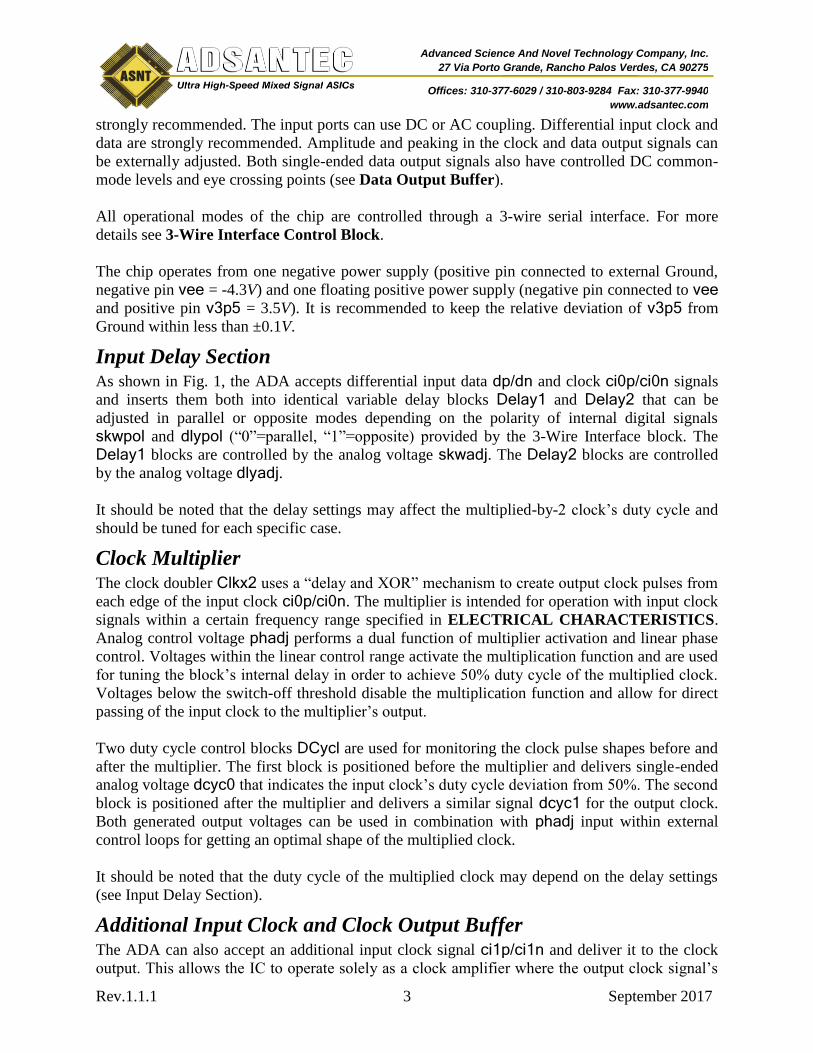
and 32Gb/s are shown in Fig. 2 and Fig. 3 respectively. Fig. 4 to Fig. 6 show this part’s
capabilities for driving a PAM4 signal.
Differential analog control voltage xadjp/xadjn can be utilized to adjust the crossing points of
single-ended output eyes. At the default state of xadjp = xadjn = 0V, the crossing points in both
direct and inverted eyes should be centered. The crossing points are moving up in the direct eye
and down in the inverted eye if xadjp = -xadjn > 0, or in the opposite directions if xadjp = -
xadjn < 0.
Fig. 2. 1-Tap Output Eye at 28Gb/s Data Rate

Rev.1.1.1 September 2017 6
Advanced Science And Novel Technology Company, Inc.
27 Via Porto Grande, Rancho Palos Verdes, CA 90275
Offices: 310-377-6029 / 310-803-9284 Fax: 310-377-9940
www.adsantec.com
Fig. 3. 1-Tap Output Eye at 32Gb/s Data Rate
Fig. 4. PAM4 Output Eye Diagram at 25.8Gb/s Data Rate
Finally, 1.0KOhm resistors are attached to both data outputs qp and qn to provide DC shifting of
the output signals. Access to the resistors is available through control pins dcqp/dcqn.
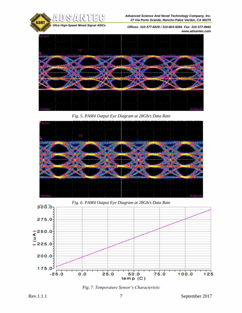
Temperature Sensor A linear temperature sensor is included on chip. Its behavior is illustrated in Fig. 7 below. The
demonstrated voltage has been generated on the internal 11KOhm resistor connected to vdd.
Rev.1.1.1 September 2017 7
Advanced Science And Novel Technology Company, Inc.
27 Via Porto Grande, Rancho Palos Verdes, CA 90275
Offices: 310-377-6029 / 310-803-9284 Fax: 310-377-9940
www.adsantec.com
Fig. 5. PAM4 Output Eye Diagram at 28Gb/s Data Rate
Fig. 6. PAM4 Output Eye Diagram at 28Gb/s Data Rate
Fig. 7. Temperature Sensor’s Characteristic

Rev.1.1.1 September 2017 8
Advanced Science And Novel Technology Company, Inc.
27 Via Porto Grande, Rancho Palos Verdes, CA 90275
Offices: 310-377-6029 / 310-803-9284 Fax: 310-377-9940
www.adsantec.com
3-Wire Interface Control Block
To reduce the physical number of digital control inputs to the ADA, a 32-bit shift register with a
3-wire input interface has been included on chip. The digital control bits applied through 3wdin
input are latched in and shifted down the register by negative edges of low-speed clock 3wcin (Bit 0/MSB first). Write enable signal 3wenin must be set to logic “1” during the data read-in
phase and then set to logic “0” to retain the shifted in values after 32 clock periods of 3wcin.
Table 2 below maps the input 32-bit word to the internal digital control signals.
Table 2. 3-Wire Interface Bit Map
Bit # Function State at
Bit=”1”/”0”
0, MSB Activation of additional 1/2 pre-buffer current in one of the Taps.
Must be ON if the amplitude in the corresponding Tap is more
than half of its maximum value (more than 1/16th of the full output
amplitude, or Aout/16).
ON/OFF in Tap 4
1 ON/OFF in Tap 3
2 ON/OFF in Tap 2
3 ON/OFF in Tap 1
4 Activation of analog-controlled sections of the Taps including the
corresponding output drivers and 1/2 pre-buffer currents.
ON/OFF in Tap 4
5 ON/OFF in Tap 3
6 ON/OFF in Tap 2
7 ON/OFF in Tap 1
8 Buffer 7 activation (Aout/8 for Tap 2 or Tap 4 as defined by Bit 16) ON/OFF
9 Buffer 6 activation (Aout/8 for Tap 2 or Tap 4 as defined by Bit 17) ON/OFF
10 Buffer 5 activation (Aout/8 for Tap 2 or Tap 3 as defined by Bit 18) ON/OFF
11 Buffer 4 activation (Aout/8 for Tap 2 or Tap 3 as defined by Bit 19) ON/OFF
12 Buffer 3 activation (Aout/8 for Tap 2 or Tap 3 as defined by Bit 20) ON/OFF
13 Buffer 2 activation (Aout/8 for Tap 2 or Tap 1 as defined by Bit 21) ON/OFF
14 Buffer 1 activation (Aout/8 for Tap 2 or Tap 1 as defined by Bit 22) ON/OFF
15 Not used
16 Buffer 7 assignment to Tap 2 or Tap 4 Tap 2 / Tap 4
17 Buffer 6 assignment to Tap 2 or Tap 4 Tap 2 / Tap 4
18 Buffer 5 assignment to Tap 2 or Tap 3 Tap 2 / Tap 3
19 Buffer 4 assignment to Tap 2 or Tap 3 Tap 2 / Tap 3
20 Buffer 3 assignment to Tap 2 or Tap 3 Tap 2 / Tap 3
21 Buffer 2 assignment to Tap 2 or Tap 1 Tap 2 / Tap 1
22 Buffer 1 assignment to Tap 2 or Tap 1 Tap 2 / Tap 1
23 Not used
24 Selection of the clock (C0 or C1) to be sent to the output C1 / C0
25 Selection of the data and clock short delay (opposite or parallel) Parallel/Opposite
26 Selection of the data and clock long delay (opposite or parallel) Parallel/Opposite
27 Activation of the Tap 4 data inversion ON/OFF
28 Activation of the Tap 3 data inversion ON/OFF
29 Activation of the Tap 2 data inversion ON/OFF
30 Activation of the Tap 1 data inversion ON/OFF
31, LSB Not used
Rev.1.1.1 September 2017 9
Advanced Science And Novel Technology Company, Inc.
27 Via Porto Grande, Rancho Palos Verdes, CA 90275
Offices: 310-377-6029 / 310-803-9284 Fax: 310-377-9940
www.adsantec.com
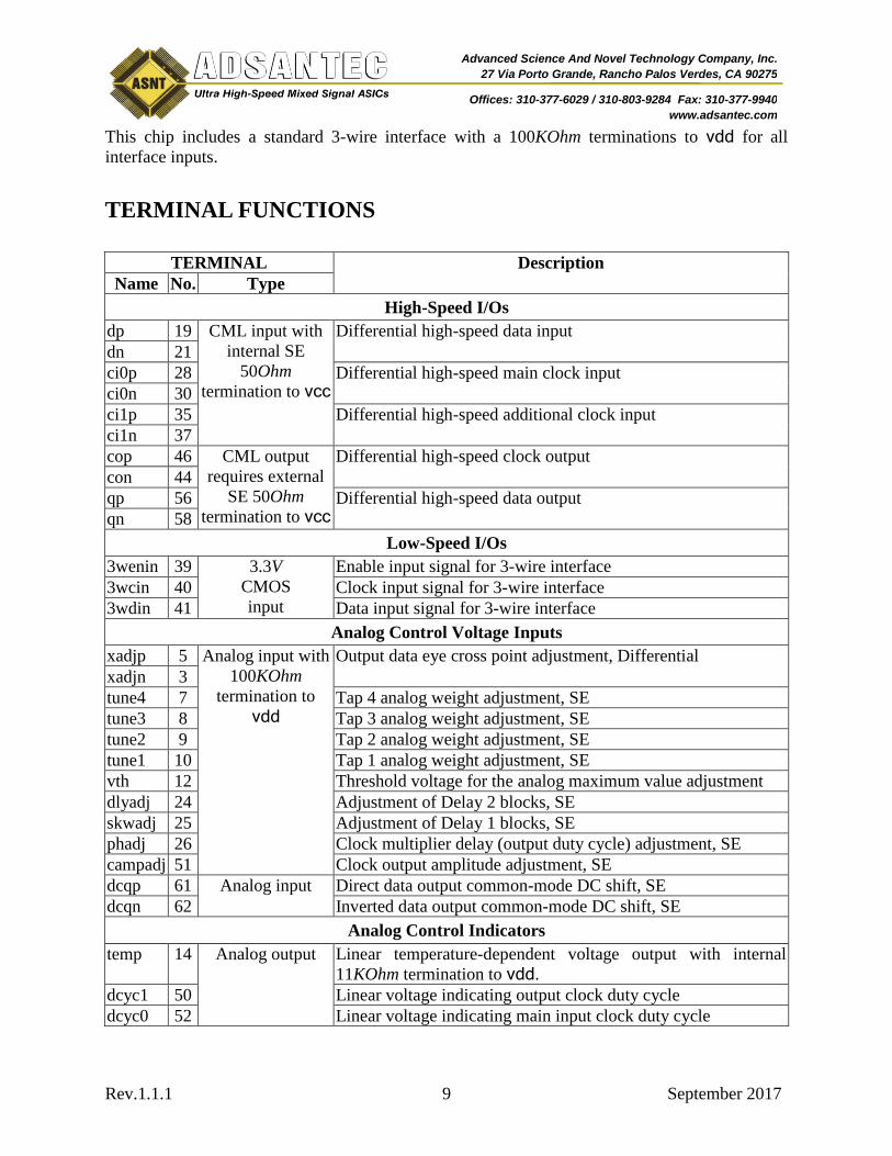
This chip includes a standard 3-wire interface with a 100KOhm terminations to vdd for all
interface inputs.
TERMINAL FUNCTIONS
TERMINAL Description
Name No. Type
High-Speed I/Os
dp 19 CML input with
internal SE
50Ohm
termination to vcc
Differential high-speed data input
dn 21
ci0p 28 Differential high-speed main clock input
ci0n 30
ci1p 35 Differential high-speed additional clock input
ci1n 37
cop 46 CML output
requires external
SE 50Ohm
termination to vcc
Differential high-speed clock output
con 44
qp 56 Differential high-speed data output
qn 58
Low-Speed I/Os
3wenin 39 3.3V
CMOS
input
Enable input signal for 3-wire interface
3wcin 40 Clock input signal for 3-wire interface
3wdin 41 Data input signal for 3-wire interface
Analog Control Voltage Inputs
xadjp 5 Analog input with
100KOhm
termination to
vdd
Output data eye cross point adjustment, Differential
xadjn 3
tune4 7 Tap 4 analog weight adjustment, SE
tune3 8 Tap 3 analog weight adjustment, SE
tune2 9 Tap 2 analog weight adjustment, SE
tune1 10 Tap 1 analog weight adjustment, SE
vth 12 Threshold voltage for the analog maximum value adjustment
dlyadj 24 Adjustment of Delay 2 blocks, SE
skwadj 25 Adjustment of Delay 1 blocks, SE
phadj 26 Clock multiplier delay (output duty cycle) adjustment, SE
campadj 51 Clock output amplitude adjustment, SE
dcqp 61 Analog input Direct data output common-mode DC shift, SE
dcqn 62 Inverted data output common-mode DC shift, SE
Analog Control Indicators
temp 14 Analog output Linear temperature-dependent voltage output with internal
11KOhm termination to vdd.
dcyc1 50 Linear voltage indicating output clock duty cycle
dcyc0 52 Linear voltage indicating main input clock duty cycle
Rev.1.1.1 September 2017 10
Advanced Science And Novel Technology Company, Inc.
27 Via Porto Grande, Rancho Palos Verdes, CA 90275
Offices: 310-377-6029 / 310-803-9284 Fax: 310-377-9940
www.adsantec.com
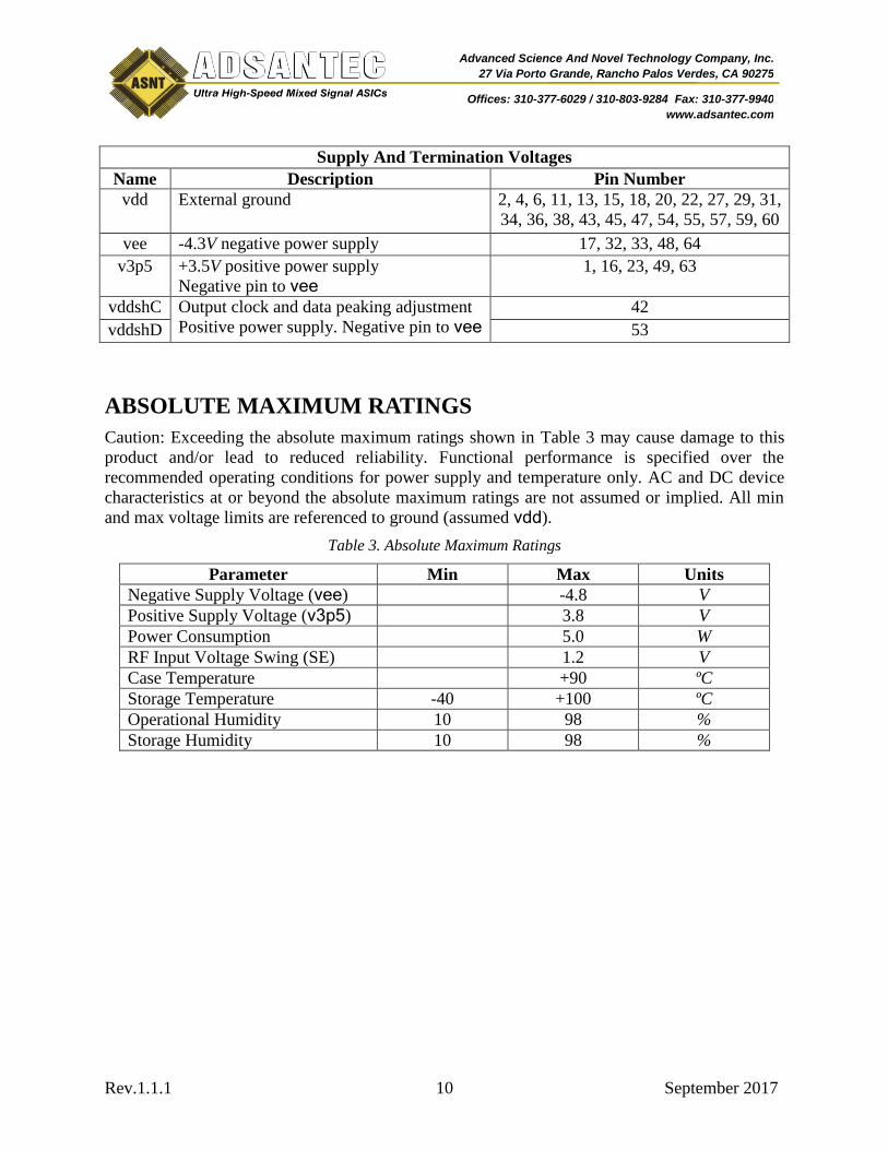
Supply And Termination Voltages
Name Description Pin Number
vdd External ground 2, 4, 6, 11, 13, 15, 18, 20, 22, 27, 29, 31,
34, 36, 38, 43, 45, 47, 54, 55, 57, 59, 60
vee -4.3V negative power supply 17, 32, 33, 48, 64
v3p5 +3.5V positive power supply
Negative pin to vee
1, 16, 23, 49, 63
vddshC Output clock and data peaking adjustment
Positive power supply. Negative pin to vee
42
vddshD 53
ABSOLUTE MAXIMUM RATINGS
Caution: Exceeding the absolute maximum ratings shown in Table 3 may cause damage to this
product and/or lead to reduced reliability. Functional performance is specified over the
recommended operating conditions for power supply and temperature only. AC and DC device
characteristics at or beyond the absolute maximum ratings are not assumed or implied. All min
and max voltage limits are referenced to ground (assumed vdd).
Table 3. Absolute Maximum Ratings
Parameter Min Max Units
Negative Supply Voltage (vee) -4.8 V
Positive Supply Voltage (v3p5) 3.8 V
Power Consumption 5.0 W
RF Input Voltage Swing (SE) 1.2 V
Case Temperature +90 ºC
Storage Temperature -40 +100 ºC
Operational Humidity 10 98 %
Storage Humidity 10 98 %

Rev.1.1.1 September 2017 11
Advanced Science And Novel Technology Company, Inc.
27 Via Porto Grande, Rancho Palos Verdes, CA 90275
Offices: 310-377-6029 / 310-803-9284 Fax: 310-377-9940
www.adsantec.com
ELECTRICAL CHARACTERISTICS
PARAMETER MIN TYP MAX UNIT COMMENTS
General Parameters
vee -4.1 -4.3 -4.5 V
vdd 0.0 V External ground
v3p5 3.4 3.5 3.6 V “-“ pin to vee
I-4.3 120 220 mA Depending on the settings of
the clock multiplier and the
clock and data amplitudes1) Iv3p5 850 1020 mA
Power 3.5 4.0 4.5 W
Junction temperature 0 50 100 °C
Data input (dp/dn)
Rate 1.0 33.5 Gb/s
SE Swing 50 200 500 mV Peak-to-peak
CM Level vdd-(SE swing)/2
Clock inputs (ci0p/ci0n, ci1p/ci1n)
Frequency (C0 input) 1.0 17 GHz Fx1 mode, any skwadj and
dlyadj 4.0 16.75 GHz Fx2 mode, skwadj and
dlyadj need tuning
SE Swing 50 200 500 mV Peak-to-peak
CM Level vdd-(SE swing)/2
Data output (qp/qn)
Rate 1.0 33.5 Gbps
SE Swing 0.0 1250 mV Peak-to-peak
CM Level vdd-0.1 vdd-0.75 V Depends on the amplitude2)
Rise/Fall Times 12 13 14 ps 20%-80%
Clock output (cop/con)
SE Swing, max 530 920 mV Pk-pk, 1.0-17GHz
160 400 mV Pk-pk, 18-32GHz
CM Level vdd-0.05 vdd-0.55 V Depends on the amplitude3)
Rise/Fall Times TBD ps 20%-80%
SE tuning ports (tune1/2/3/4, skwadj, dlyadj, phadj, campadj) Linear control voltage vdd-2 vdd V
Switch-off threshold vdd-2 V
Cross point control (xadjp/xadjn)
Differential voltage range vdd-8.0 vdd+8.0 V ±4V at each input
CM Level vdd
Current in/out of the pin +4 / -4 mA at +4V / -4V
Threshold control (vth)
Voltage range vdd-2 vdd V
DC common mode voltage control (dcqp/dcqn)
Voltage range vee vdd V

Rev.1.1.1 September 2017 12
Advanced Science And Novel Technology Company, Inc.
27 Via Porto Grande, Rancho Palos Verdes, CA 90275
Offices: 310-377-6029 / 310-803-9284 Fax: 310-377-9940
www.adsantec.com
PARAMETER MIN TYP MAX UNIT COMMENTS
Externally Controlled Operational Ranges
Clock-to-Data skew -30 +30 ps opposite skwadj control
Clock and Data delay 0 +30 ps paralllel skwadj control
Clock-to-Data skew -45 +45 ps opposite dlyadj control
Clock and Data delay 0 +45 ps paralllel dlyadj control
Output eye cross point -25 +25 % of the eye amplitude
PARAMETER MIN TYP MAX UNIT COMMENTS
Variable supply voltages (vddshc, vddshd)
Voltage range 2.8 4.3 V “-“ pin to vee
Ivddshd 2.2 mA All 4 taps active
Ivddshc 1.1 mA
Duty Cycle Indicator (dcyc0/dcyc1)
Voltage range vdd-3.3 vdd-0.8 V
Temperature Sensor (temp)
Voltage range vdd-3.3 vdd-2.3 V
3-Wire Inputs (3wdin, 3wcin, 3wenin)
High voltage level vdd-0.2 vdd V
Low voltage level vdd-3.3 vdd-3.1 V
Clock speed 350 400 MHz
Power Supply Currents
(Preliminary Data, for Reference Only)
co amplitude q amplitude Clock multiplier I-4.3, mA Iv3p5, mA
min min off (Fx1) 120 850
min min on (Fx2) 120 920
min max off (Fx1) 180 880
min max on (Fx2) 180 950
max min off (Fx1) 160 930
max min on (Fx2) 160 1000
max max off (Fx1) 220 950
max max on (Fx2) 220 1020

Rev.1.1.1 September 2017 13
Advanced Science And Novel Technology Company, Inc.
27 Via Porto Grande, Rancho Palos Verdes, CA 90275
Offices: 310-377-6029 / 310-803-9284 Fax: 310-377-9940
www.adsantec.com
Data Output Common Mode Voltage Levels
(Preliminary Data, for Reference Only)
Amplitude VCM, V
Amplitude VCM, V
Total, mV Digital Analog, mV Total, mV Digital Analog, mV
150 0 min vdd-0.089 790 4Aout/8 min vdd-0.461
150 Aout/8 max vdd-0.182 790 5Aout/8 max vdd-0.554
310 Aout/8 min vdd-0.182 950 5Aout/8 min vdd-0.554
310 2Aout/8 max vdd-0.275 950 6Aout/8 max vdd-0.647
470 2Aout/8 min vdd-0.275 1100 6Aout/8 min vdd-0.647
470 3Aout/8 max vdd-0.368 1100 7Aout/8 max vdd-0.740
630 3Aout/8 min vdd-0.368 1250 7Aout/8 min vdd-0.740
630 4Aout/8 max vdd-0.461
Clock Output Common Mode Voltage Levels
(Preliminary Data, for Reference Only)
Amplitude, mV 100 200 300 400 500 600 700 750
VCM, V vdd-0.07 vdd-0.14 vdd-0.21 vdd-0.28 vdd-0.35 vdd-0.42 vdd-0.49 vdd-0.54
PACKAGE INFORMATION
The chip die is housed in a custom 64-pin CQFP package. The dimensioned drawings are shown
in Fig. 8.
The package provides a center heat slug located on its back side to be used for heat dissipation.
ADSANTEC recommends for this section to be soldered to the vdd plain, which is ground for a
negative supply, or power for a positive supply.
The part’s identification label is ASNT6119B-KMF. The first 9 characters of the name before
the dash identify the bare die including general circuit family, fabrication technology, specific
circuit type, and part version while the 3 characters after the dash represent the package’s
manufacturer, type, and pin out count.
This device complies with the Restriction of Hazardous Substances (RoHS) per EU 2002/95/EC
for all six substances.

Rev.1.1.1 September 2017 14
Advanced Science And Novel Technology Company, Inc.
27 Via Porto Grande, Rancho Palos Verdes, CA 90275
Offices: 310-377-6029 / 310-803-9284 Fax: 310-377-9940
www.adsantec.com
Fig. 8. CQFP 64-Pin Package Drawing (All Dimensions in mm)

Rev.1.1.1 September 2017 15
Advanced Science And Novel Technology Company, Inc.
27 Via Porto Grande, Rancho Palos Verdes, CA 90275
Offices: 310-377-6029 / 310-803-9284 Fax: 310-377-9940
www.adsantec.com
REVISION HISTORY
Revision Date Changes
1.1.1 09-2017 Corrected frequency of operation
Updated electrical characteristics
1.0.1 09-2017 Initial release


![16 Annual Report 2010-2011 - KMF BUILDERSkmfbuilders.com/images/16_th_Annual_report/KMFBUILD_11_final[1].… · KMF BUILDERS & DEVELOPERS LIMITED Annual Report 2010-11 1 NOTICE Notice](https://static.fdocuments.in/doc/165x107/5ead91be80f40046fa416b9b/16-annual-report-2010-2011-kmf-1-kmf-builders-developers-limited-annual.jpg)


