ASML HOLDING NV (Form: 6-K, Filing Date:...
98
Business Address DE RUN 6501 DR VELDHOVEN P7 5504 31402683000 Mailing Address P.O. BOX 324 AH VELDHOVEN P7 5500 SECURITIES AND EXCHANGE COMMISSION FORM 6-K Current report of foreign issuer pursuant to Rules 13a-16 and 15d-16 Amendments Filing Date: 2008-06-05 | Period of Report: 2008-06-05 SEC Accession No. 0001156973-08-000602 (HTML Version on secdatabase.com) FILER ASML HOLDING NV CIK:937966| IRS No.: 000000000 | Fiscal Year End: 1231 Type: 6-K | Act: 34 | File No.: 001-33463 | Film No.: 08881930 SIC: 3559 Special industry machinery, nec Copyright © 2012 www.secdatabase.com . All Rights Reserved. Please Consider the Environment Before Printing This Document
Transcript of ASML HOLDING NV (Form: 6-K, Filing Date:...

Business AddressDE RUN 6501DR VELDHOVEN P7 550431402683000
Mailing AddressP.O. BOX 324AH VELDHOVEN P7 5500
SECURITIES AND EXCHANGE COMMISSION
FORM 6-KCurrent report of foreign issuer pursuant to Rules 13a-16 and 15d-16 Amendments
Filing Date: 2008-06-05 | Period of Report: 2008-06-05SEC Accession No. 0001156973-08-000602
(HTML Version on secdatabase.com)
FILERASML HOLDING NVCIK:937966| IRS No.: 000000000 | Fiscal Year End: 1231Type: 6-K | Act: 34 | File No.: 001-33463 | Film No.: 08881930SIC: 3559 Special industry machinery, nec
Copyright © 2012 www.secdatabase.com. All Rights Reserved.Please Consider the Environment Before Printing This Document

SECURITIES AND EXCHANGE COMMISSIONWashington, D.C. 20549
FORM 6-K
REPORT OF A FOREIGN ISSUERPURSUANT TO RULE 13A-16 OR 15D-16
OF THE SECURITIES EXCHANGE ACT OF 1934For May 2008
ASML Holding N.V.De Run 6501
5504 DR VeldhovenThe Netherlands
(Address of principal executive offices)
Indicate by check mark whether the registrant files or will file annual reports under cover of Form 20-F or Form 40-F.
Form 20-F þ Form 40-F o
Indicate by check mark whether the registrant by furnishing the information contained in this Form is also thereby furnishing the informationto the Commission pursuant to Rule 12g3-2(b) under the Securities Exchange Act of 1934.
Yes o No þ
If �Yes� is marked, indicate below the file number assigned to the registrant in connection with Rule 12g3-2(b):
Copyright © 2012 www.secdatabase.com. All Rights Reserved.Please Consider the Environment Before Printing This Document

Exhibits
99.1 Merrill Lynch Technology Conference 2008, �ASML Continues to Execute its Leadership Strategy and Expects Gradual Order Pick-up,� presentation dated May 6, 2008;
99.2 The Confab Technology Conference, �Next Generation Lithography � The Road to Cost-Effective Shrink,� presentation dated May 20,2008;
99.3 FBR Capital Markets � 12th Annual Spring Investor Conference, �ASML Continues to Execute its Leadership Strategy,� presentationdated May 28, 2008.
�Safe Harbor� Statement under the U.S. Private Securities Litigation Reform Act of 1995: the matters discussed in this document mayinclude forward-looking statements, including statements made about our outlook, realization of backlog, IC unit demand, financial results,average sales price, gross margin and expenses. These forward looking statements are subject to risks and uncertainties including, but notlimited to: economic conditions, product demand and semiconductor equipment industry capacity, worldwide demand and manufacturingcapacity utilization for semiconductors (the principal product of our customer base), competitive products and pricing, manufacturingefficiencies, new product development and customer acceptance of new products, ability to enforce patents and protect intellectual propertyrights, the outcome of intellectual property litigation, availability of raw materials and critical manufacturing equipment, trade environment,changes in exchange rates and other risks indicated in the risk factors included in ASML�s Annual Report on Form 20-F and other filings withthe U.S. Securities and Exchange Commission.
SIGNATURES
Pursuant to the requirements of the Securities Exchange Act of 1934, the registrant has duly caused this report to be signed on its behalf bythe undersigned, thereunto duly authorized.
ASML HOLDING N.V. (Registrant)
Date: June 5, 2008 By: /s/ Peter T.F.M. WenninkPeter T.F.M. WenninkExecutive Vice President and Chief FinancialOfficer
2
Copyright © 2012 www.secdatabase.com. All Rights Reserved.Please Consider the Environment Before Printing This Document

Merrill Lynch Technology Conference 2008 ASML continues to execute its leadership strategy and expects gradual order pick-up Craig De Young VP Investor Relations and Corporate Communications New York City - May 06, 2008
Copyright © 2012 www.secdatabase.com. All Rights Reserved.Please Consider the Environment Before Printing This Document

Safe Harbor "Safe Harbor" Statement under the US Private Securities Litigation Reform Act of 1995: the matters discussed in this document may include forward- looking statements, including statements made about our outlook, realization of backlog, IC unit demand, financial results, average sales price, gross margin and expenses. These forward looking statements are subject to risks and uncertainties including, but not limited to: economic conditions, product demand and semiconductor equipment industry capacity, worldwide demand and manufacturing capacity utilization for semiconductors (the principal product of our customer base), competitive products and pricing, manufacturing efficiencies, new product development and customer acceptance of new products, ability to enforce patents and protect intellectual property rights, the outcome of intellectual property litigation, availability of raw materials and critical manufacturing equipment, trade environment, changes in exchange rates and other risks indicated in the risk factors included in ASML's Annual Report on Form 20-F and other filings with the US Securities and Exchange Commission.
Copyright © 2012 www.secdatabase.com. All Rights Reserved.Please Consider the Environment Before Printing This Document

ASML - the world's largest supplier of lithography equipment Source: Semi & ASML Leadership in immersion for volume chip manufacturing Canon 11% ASML 65% Nikon 24% KLA Tencor ASML Tokyo Electron Lam Research Applied Materials Revenue evolution Top 5 semiconductor equipment suppliers - 2007 Market share 2007
Copyright © 2012 www.secdatabase.com. All Rights Reserved.Please Consider the Environment Before Printing This Document

The Market
Copyright © 2012 www.secdatabase.com. All Rights Reserved.Please Consider the Environment Before Printing This Document
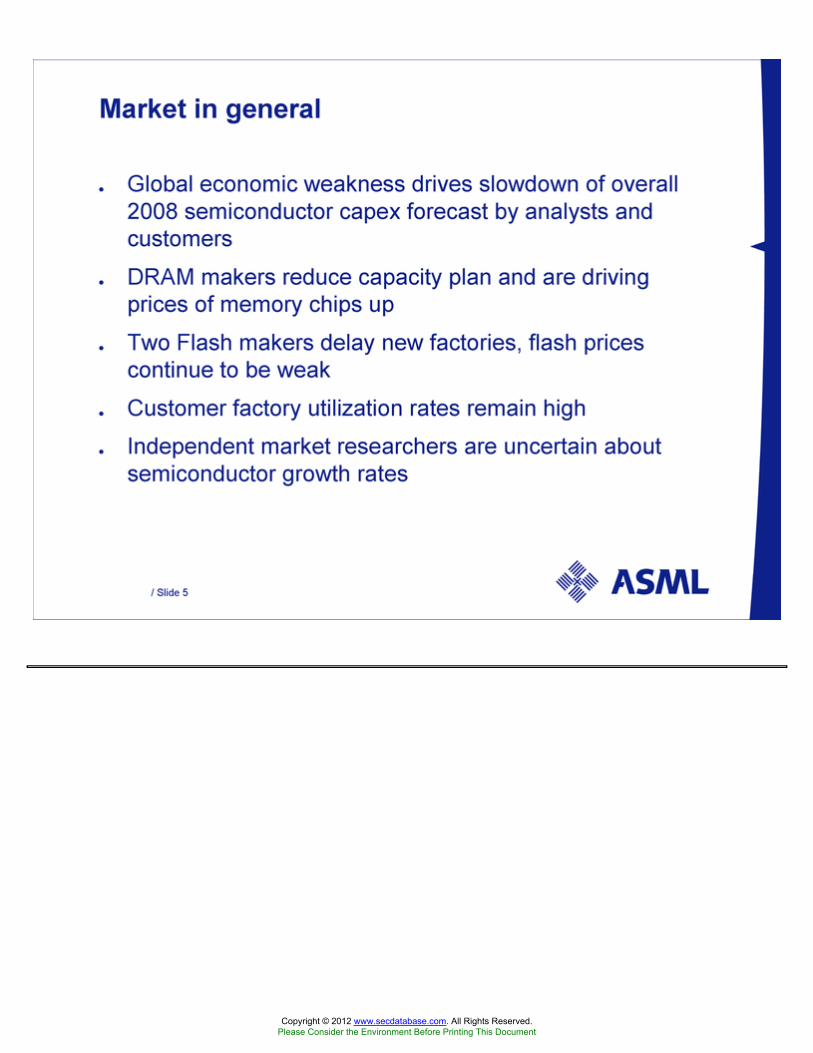
Market in general Global economic weakness drives slowdown of overall 2008 semiconductor capex forecast by analysts and customers DRAM makers reduce capacity plan and are driving prices of memory chips up Two Flash makers delay new factories, flash prices continue to be weak Customer factory utilization rates remain high Independent market researchers are uncertain about semiconductor growth rates
Copyright © 2012 www.secdatabase.com. All Rights Reserved.Please Consider the Environment Before Printing This Document

ASML affected by changing market environment Recent capacity delay decisions by one DRAM factory expansion and two new Flash factories impact Q1 orders and '08 outlook Rationalization efforts amongst Taiwanese DRAM players ongoing Overall economic growth uncertainty delaying capex decisions for Foundries Demand for immersion tools remain strong
Copyright © 2012 www.secdatabase.com. All Rights Reserved.Please Consider the Environment Before Printing This Document

ASML's assessment of 2008 worldwide lithography demand March 2008 ASML shipped 260 machines in 2007 with ASP of � 12.9 million ASML expects market share gains and substantial ASP growth in 2008 Numbers include new and used equipment Source: ASML April 2008 April 2008
Copyright © 2012 www.secdatabase.com. All Rights Reserved.Please Consider the Environment Before Printing This Document

Industry analyst 2008 memory forecasts Source: ASML MCC Unit Growth Time of Forecast DRAM Unit Growth NAND Unit Growth Gartner IC Insights VLSIR
Copyright © 2012 www.secdatabase.com. All Rights Reserved.Please Consider the Environment Before Printing This Document
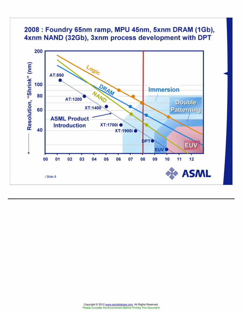
2008 : Foundry 65nm ramp, MPU 45nm, 5xnm DRAM (1Gb), 4xnm NAND (32Gb), 3xnm process development with DPT 10 12 Resolution, "Shrink" (nm) 200 100 80 60 40 Logic DRAM NAND 11 07 09 08 04 06 05 01 03 02 00 ASML Product Introduction XT:1400 XT:1700i AT:1200 AT:850 Double Patterning XT:1900i EUV Immersion EUV DPT
Copyright © 2012 www.secdatabase.com. All Rights Reserved.Please Consider the Environment Before Printing This Document

65nm Pilot 90nm Pilot N90 Qualification Period N90 Production Ramp Source: TSMC Quarterly Reports FOUNDRY Sales by process technology: 65nm starts volume ramp in 2008
Copyright © 2012 www.secdatabase.com. All Rights Reserved.Please Consider the Environment Before Printing This Document

FOUNDRY Bi-annual capacity increase pattern* suggests improved 2H/08 Foundry utilization triggers ASML litho equipment purchases Source: ASML MCC (SAP-IFP update 12/07) * Utilization seems to drop mainly as result of capacity additions. If pattern holds, foundry will likely add capacity again in 2008. This is not a forecast. 2002 2003 2004 2005 2006 2007 2008 TWINSCAN Add Point
Copyright © 2012 www.secdatabase.com. All Rights Reserved.Please Consider the Environment Before Printing This Document

ASML technology leader
Copyright © 2012 www.secdatabase.com. All Rights Reserved.Please Consider the Environment Before Printing This Document

Source: ASML Immersion technology used in volume production for 55 nm resolution and beyond ASML immersion installed base 86 tools 25 in the US 53 in ASIA, (16 in Japan) 8 in Europe
Copyright © 2012 www.secdatabase.com. All Rights Reserved.Please Consider the Environment Before Printing This Document
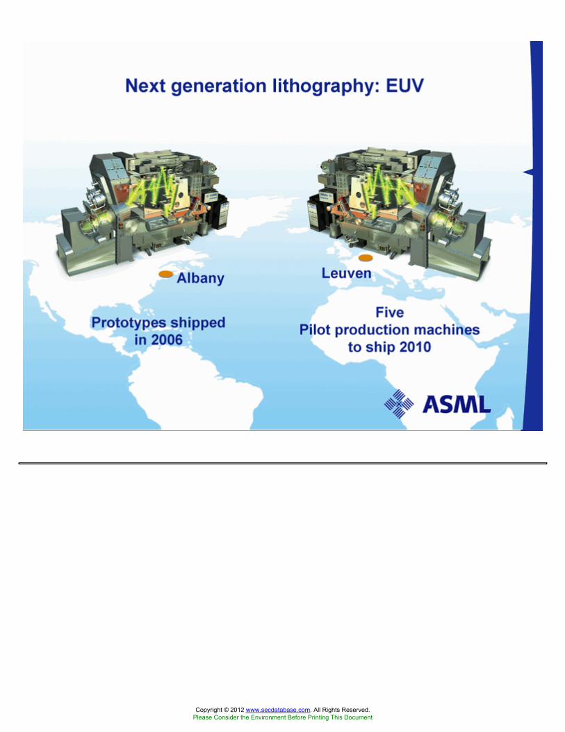
Next generation lithography: EUV Prototypes shipped in 2006 Five Pilot production machines to ship 2010 Albany Leuven
Copyright © 2012 www.secdatabase.com. All Rights Reserved.Please Consider the Environment Before Printing This Document

/ Slide 15 EUVL Roadmap down to 11 nm support 22 nm and 16 nm node with a single projection system same projection system, enhanced off-axis illumination implementation volume production Res 11 nm 16 nm 22 nm 27 nm 2014 2015 2013 2010 2011 2012 0.32 NA +off axis illumination 0.32 NA, 3 nm OVL, >100 wph 0.25 NA, 4 nm OVL 0.4x NA
Copyright © 2012 www.secdatabase.com. All Rights Reserved.Please Consider the Environment Before Printing This Document

/ Slide 16 Strong DPT EUV DFM supported low k1, light DPT EUV Jan-02 Jan-03 Jan-04 Jan-05 Jan-06 Jan-07 Jan-08 Jan-09 Jan-10 Jan-11 Jan-12 Jan-13 Jan-14 Year of Production Start* Resolution, "Shrink" [nm] 100 80 60 Logic NAND Flash DRAM 30 20 50 *Process development 1.5 ~ 2 years in advance (updated 12/07) 200 Double patterning will bridge the gap between single exposure 193 nm immersion and EUV AT:1200 XT:1400 XT:1900i Next EUV ASML product Introduction 40 XT:1700i
Copyright © 2012 www.secdatabase.com. All Rights Reserved.Please Consider the Environment Before Printing This Document

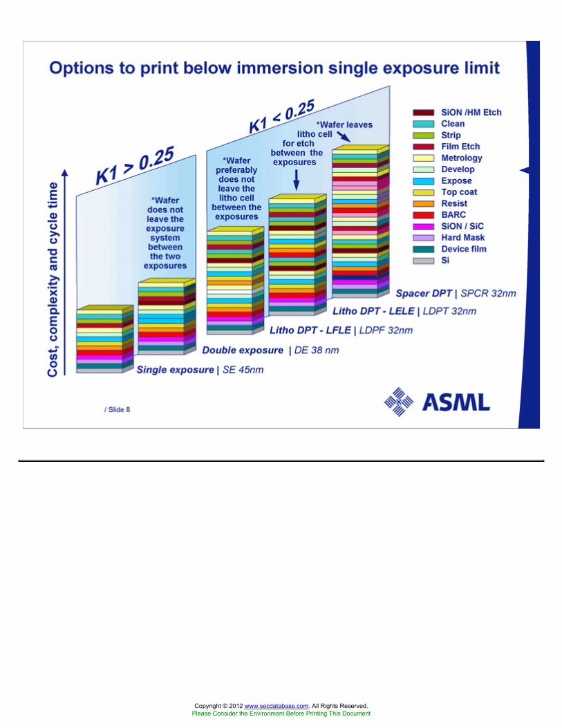
/ Slide 17 Spacer DPT | SPCR 32nm Litho DPT - LELE | LDPT 32nm Litho DPT - LFLE | LDPF 32nm Double exposure | DE 38 nm SiON /HM Etch Clean Strip Film Etch Metrology Develop Expose Top coat Resist BARC SiON / SiC Hard Mask Device film Si Single exposure | SE 45nm Options to print below immersion single exposure limit Cost, complexity and cycle time *Wafer does not leave the exposure system between the two exposures *Wafer preferably does not leave the litho cell between the exposures *Wafer leaves litho cell for etch between the exposures
Copyright © 2012 www.secdatabase.com. All Rights Reserved.Please Consider the Environment Before Printing This Document
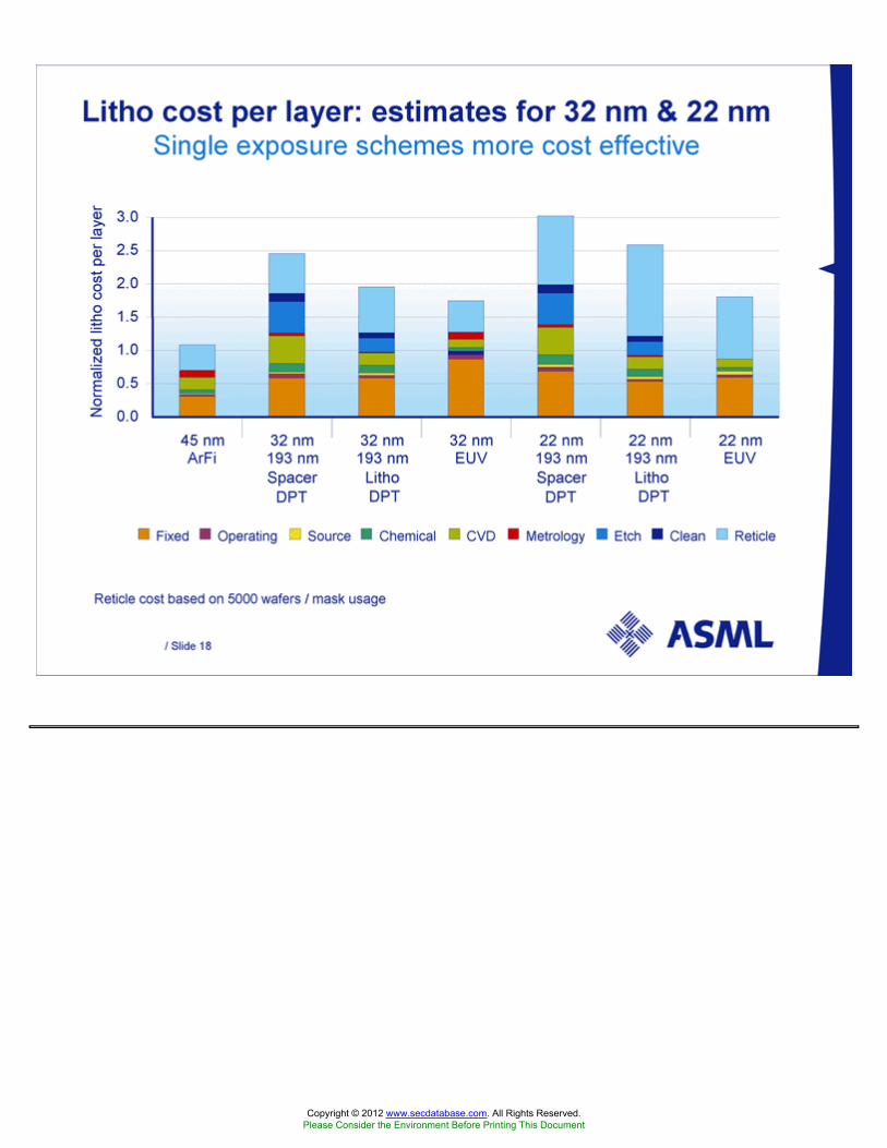
/ Slide 18 Litho cost per layer: estimates for 32 nm & 22 nm Single exposure schemes more cost effective Reticle cost based on 5000 wafers / mask usage Fixed Operating Source Chemical CVD Metrology Etch Clean Reticle 0.0 0.5 1.0 1.5 2.0 2.5 3.0 45 nm 32 nm 32 nm 32 nm 22 nm 22 nm 22 nm ArFi 193 nm Spacer DPT 193 nm Litho DPT EUV 193 nm Spacer DPT 193 nm Litho DPT EUV Normalized litho cost per layer
Copyright © 2012 www.secdatabase.com. All Rights Reserved.Please Consider the Environment Before Printing This Document

Business summary
Copyright © 2012 www.secdatabase.com. All Rights Reserved.Please Consider the Environment Before Printing This Document

Q1 results 8th consecutive quarter with sales over � 900 million Solid operating margin of 20.5% Cash generation � 263 million from operations Backlog at �1,167 million, 65 systems Booked 26 systems Shipped 14 immersion tools Record average selling price for new shipped systems of � 18.7 million
Copyright © 2012 www.secdatabase.com. All Rights Reserved.Please Consider the Environment Before Printing This Document

Total net sales M� 1,543 2,465 2,529 3,597 3,768 *2007 numbers are adjusted retrospectively with respect to the change in accounting policy.
Copyright © 2012 www.secdatabase.com. All Rights Reserved.Please Consider the Environment Before Printing This Document

Net sales breakdown in value: Q1 2008 End-use Foundry 13% Numbers have been rounded for readers' convenience Technology KrF 14% i-Line 3% ArF dry 32% USA 24% Taiwan 15% Korea 32% Japan 7% Europe 7% Sales in Units Region Other 1% China 14% Memory 64% IDM 23% ArF Immersion 51%
Copyright © 2012 www.secdatabase.com. All Rights Reserved.Please Consider the Environment Before Printing This Document

Backlog lithography in value per March 30th, 2008 Total value M� 1,167 = 65 systems Technology i-Line 3% KrF 9% ArF dry 31% Region USA 20% Taiwan 13% Korea 30% Other 6% Europe 13% Japan 9% China 9% End-use Memory 56% IDM 30% Foundry 14% Numbers have been rounded for readers' convenience ArF immersion 57%
Copyright © 2012 www.secdatabase.com. All Rights Reserved.Please Consider the Environment Before Printing This Document

Outlook
Copyright © 2012 www.secdatabase.com. All Rights Reserved.Please Consider the Environment Before Printing This Document

Q2 2008 outlook ASML expects to ship 42 systems ASP for new + refurbished systems expected to be � 17.0 million Gross margin approximately 40% R&D is expected at � 130 million net of credit SG&A is expected at � 58 million Given current market weakness, we are trimming Manufacturing and SG&A variable costs for 2008 second half while keeping R&D stable
Copyright © 2012 www.secdatabase.com. All Rights Reserved.Please Consider the Environment Before Printing This Document

Outlook Order pattern translates into weaker net sales for next 2 quarters We expect gradual unit order pick-up from Q2 onwards, due to: Improvements in memory supply/demand balance Volume production ramps of 45nm node Flash memory to start in H2 2008 Foundry contribution ASML's market share gains Due to advanced technology tool mix, Q2 bookings value increase will be significant
Copyright © 2012 www.secdatabase.com. All Rights Reserved.Please Consider the Environment Before Printing This Document

Copyright © 2012 www.secdatabase.com. All Rights Reserved.Please Consider the Environment Before Printing This Document

Next Generation Lithography The road to cost-effective shrink Martin van den Brink Executive Vice President Marketing & Technology May 20, 2008
Copyright © 2012 www.secdatabase.com. All Rights Reserved.Please Consider the Environment Before Printing This Document
Agenda Shrink roadmap Progress in immersion lithography A holistic approach to extend immersion lithography EUV the next production worthy shrink technology Economics of advanced lithography
Copyright © 2012 www.secdatabase.com. All Rights Reserved.Please Consider the Environment Before Printing This Document

Jan - 02 Jan - 03 Jan - 04 Jan - 05 Jan - 06 Jan - 07 Jan - 08 Jan - 09 Jan - 10 Jan - 11 Jan - 12 Jan - 13 Jan - 14 Year of production start* Resolution, "Shrink" [nm] 100 80 60 40 Logic NAND Flash DRAM 30 20 50 *Process development 1.5 ~ 2 years in advance (updated 12/07) 200 Shrink will continue (based on the average of multiple customers' input)
Copyright © 2012 www.secdatabase.com. All Rights Reserved.Please Consider the Environment Before Printing This Document

Most likely litho roadmap Half pitch (nm) Half pitch (nm) Half pitch (nm) Half pitch (nm) Half pitch (nm) 100 65 45 32 22 16 11 Year Year Year 2005 2007 2009 2011 2013 2015 ? (nm) NA NA 248 0.93 0.93 0.38 0.38 193 0.93 0.93 0.31 1.20 1.20 0.40 0.28 1.35 1.35 0.31 0.22 0.15 1.55 1.55 0.26 0.18 13.5 0.25 0.25 0.59 0.41 0.35 0.35 0.57 0.41 0.45 0.45 0.53 0.37 most likely opportunity
Copyright © 2012 www.secdatabase.com. All Rights Reserved.Please Consider the Environment Before Printing This Document

Agenda Shrink roadmap Progress in immersion lithography A holistic approach to extend immersion lithography EUV the next production worthy shrink technology Economics of advanced lithography
Copyright © 2012 www.secdatabase.com. All Rights Reserved.Please Consider the Environment Before Printing This Document

Immersion 1.35 NA scalable to 38 nm SGL WL1 ...32 parallel word lines Focus: 40 nm 38 nm -20 nm 0 +20 nm +40 nm -50 nm -20 nm 0 +20 nm +40 nm -30 nm Focus: NA = 1.35 Dipole-X-35 ? = 0.82/0.97 Y Polarization 6% Att PSM mask
Copyright © 2012 www.secdatabase.com. All Rights Reserved.Please Consider the Environment Before Printing This Document

Shrink roadmap Progress in immersion lithography A holistic approach to extend immersion lithography Double patterning Optimize performance using computational lithography Reduce variability using intra-field litho correction EUV the next production worthy shrink technology Economics of advanced lithography Agenda
Copyright © 2012 www.secdatabase.com. All Rights Reserved.Please Consider the Environment Before Printing This Document
Spacer DPT | SPCR 32nm Litho DPT - LELE | LDPT 32nm Litho DPT - LFLE | LDPF 32nm Double exposure | DE 38 nm SiON /HM Etch Clean Strip Film Etch Metrology Develop Expose Top coat Resist BARC SiON / SiC Hard Mask Device film Si Single exposure | SE 45nm Options to print below immersion single exposure limit Cost, complexity and cycle time *Wafer does not leave the exposure system between the two exposures *Wafer preferably does not leave the litho cell between the exposures *Wafer leaves litho cell for etch between the exposures
Copyright © 2012 www.secdatabase.com. All Rights Reserved.Please Consider the Environment Before Printing This Document

Single exposure (like EUV): lowest process complexity and most relaxed litho requirements, suitable for 1D and 2D scaling, logic and all memory Real CD is smaller than target CD. Error caused by litho step CD error during litho process steps will result in smaller lines Extra CD errors are created during etch step combined with litho CD error to a final CD error Target CD litho Target CD < 10% CD CD determined by 2 error components litho and etch: ^CDlitho < 7% of CD Overlay < 20% of CD
Copyright © 2012 www.secdatabase.com. All Rights Reserved.Please Consider the Environment Before Printing This Document

Litho1 Standard resist "Freezing" process first developed image: Coat first developed (shown) Thermal treatment Pos/Neg resist Other post development treatment Litho 2 Coat, expose, develop 2nd pattern Litho double patterning: Litho-Freeze-Litho-Etch Litho quality yet below required 32 nm performance but lowest cost opportunity: wafer will not leave the litho cell between the 2 exposures 32 nm Litho1 + Litho2 After etch into 60nm poly 2nd 1st 2nd 1st Data generated in collaboration with IMEC
Copyright © 2012 www.secdatabase.com. All Rights Reserved.Please Consider the Environment Before Printing This Document

Litho double patterning: Litho-Etch-Litho-Etch Suitable for 1D and 2D scaling, logic and all memory 1st Photo CD errors during litho will result in smaller/larger lines 1st Etch+CD trim Extra CD errors could take place 2nd Photo Overlay error translates into CD error between lines 2nd etch+CD trim 2nd pattern with CD errors from 2nd etch/trim and overlay 32 nm lines/96 nm spaces 32 nm lines/32 nm spaces Real CD litho is smaller than target CD litho. Error caused by litho Target CD litho Final CD < 10% CD CD determined by 8 error components; 2 x litho, 2 x etch and overlay: ^CDlitho < 3.5% of CD Overlay < 7% of CD
Copyright © 2012 www.secdatabase.com. All Rights Reserved.Please Consider the Environment Before Printing This Document

CD determined by 11 error components; litho, etch, spacer deposition, trim and final etch: ^CDlitho < 3 % of CD Overlay < 20% of CD Spacer double patterning litho requirements 1D scaling only, suitable for Flash Real CD is smaller than target CD. Error caused by litho and etch trim patterning steps Sacrificial line patterning: A CD error during litho and etch process steps will result in smaller lines Target CD litho Final CD < 10%CD Line CD error propagates during spacer uniform deposition and etched back Initial CD error becomes a pitch variation on the final pattern Data generated in collaboration with IMEC
Copyright © 2012 www.secdatabase.com. All Rights Reserved.Please Consider the Environment Before Printing This Document

Negative spacer flow for NAND periphery G After etch Trim mask B Pattern split C 1st litho/etch D 1st spacer deposition A design Based on Soo-Han Choi et al. | SPIE Ref. 5377-63 "Simulation-based critical area extraction and litho-friendly layout design for low k1 lithography", F 2nd litho/Trim This is the overlap of the trim mask and layout in E E 2nd film dep
Copyright © 2012 www.secdatabase.com. All Rights Reserved.Please Consider the Environment Before Printing This Document

Double patterning requires better and more lithography Litho exposure equipment parameter as percentage of CD Single exposure Litho double patterning Spacer double patterning ^CD 7% 3.5% 3% Overlay (depending on DFM) 20% 7% 7-20%* # mask steps 1 2 2-3 # process steps relative to single exposure 1 2 3-4 Application 2D, all 2D, all 1D, mainly memory * Depending on the amount of "Design For Manufacturing" effort
Copyright © 2012 www.secdatabase.com. All Rights Reserved.Please Consider the Environment Before Printing This Document
Shrink roadmap Progress in immersion lithography A holistic approach to extend immersion lithography Double patterning Optimize performance using computational lithography Reduce variability using intra-field litho correction EUV the next production worthy shrink technology Economics of advanced lithography Agenda
Copyright © 2012 www.secdatabase.com. All Rights Reserved.Please Consider the Environment Before Printing This Document

Design For Manufacturing DFM Application Specific Manufacturing Design space Manufacturing space Litho aware design constraints OPC & RETs: PSM, DPT, Scatterbars, DDL verification Application specific tuning Source-Mask Optimization Low k1: High design to wafer integration Low k1 (<0.4): Integration of design, mask and lithography processes
Copyright © 2012 www.secdatabase.com. All Rights Reserved.Please Consider the Environment Before Printing This Document

Scanner Matcher Product Portfolio (beta Q3 07) Full Chip plug in Matching service Matching service
Copyright © 2012 www.secdatabase.com. All Rights Reserved.Please Consider the Environment Before Printing This Document

Matching using through pitch structures not adequate Extended structure set required to capture all variations Structure type Structure type CD matching [nm] Immersion matching performance between 1.2 NA and 1.35 NA system -10 -5 0 5 10 A B C A B C A B C A B C A B C A B C Pitch Bar Line Bar Space EOL EOLT Gen2D A: 1900i-1700i Untuned baseline matching B: 1900i-1700i Tuning based on pitch lines only C: 1900i-1700i Tuning based on all patterns Data generated in collaboration with IMEC
Copyright © 2012 www.secdatabase.com. All Rights Reserved.Please Consider the Environment Before Printing This Document

Integration of computational lithography tools Source Mask Optimization & Litho double patterning Low K1 integration of DPT, SMO & full chip verification Traditional single clip Source Mask Optimization Split 1 Split 2 Source Mask Optimization Cell design PW verification Split 1 Split 2 Final Source 1 DOF =98nm, EL = 10% Logic part of design SRAM + Logic optimized source Split 1 Split 2 Full-chip OPC & verification verification verification DOF = 82 nm EL = 10% Final source PW verification with Source 1 DOF =98 nm, EL = 5% Final PW has acceptable size
Copyright © 2012 www.secdatabase.com. All Rights Reserved.Please Consider the Environment Before Printing This Document

Shrink roadmap Progress in immersion lithography A holistic approach to extend immersion lithography Double patterning Optimize performance using computational lithography Reduce variability using intra-field litho correction EUV the next production worthy shrink technology Economics of advanced lithography Agenda
Copyright © 2012 www.secdatabase.com. All Rights Reserved.Please Consider the Environment Before Printing This Document

Improved (integrated) metrology & intra and inter field control loops to drive CD and Overlay required develop Track Off-line metrology CD, OVL, Focus & Dose Film thickness Feedback Example intrafield CD control: "Dose mapper" Inter-field: Dose per Field Intra-field Y-scan: Dosicom -2% 0% 2% 4% -4% -14 -7 0 7 14 Dose Change Dose on wafer Requested dose Scan position [mm] Intra-field X-slit: Unicom -2% 0% 2% -13 0 13 Slit position [mm] Intensity change Filter Position Exposure Slit Litho only can provide intra wafer/field control coat Track Metrology system
Copyright © 2012 www.secdatabase.com. All Rights Reserved.Please Consider the Environment Before Printing This Document

High precision and productive metrology: angle-resolved scatterometry vs spectroscopic Multi wavelength 2D vs 0D pupil detection for angle-resolved scatterometry for more process robust metrology ? I(?) 30x more photons for angle-based scatterometry for more productivity Spectrometer grating Beam splitter 1D CCD light source wafer Pupil stop light source wafer Interference filter 2D CCD camera Beam splitter Angle-resolved scatterometry Spectroscopic scatterometry I(?1) I(?2 )
Copyright © 2012 www.secdatabase.com. All Rights Reserved.Please Consider the Environment Before Printing This Document

Litho patterning process control for CD and Overlay of 32 nm, using angle-resolved scatterometry Overlay between litho 1 and 2 DoseMapper recipe Line1 Line2 Raw etched poly CDU DoseMapper recipe Optimum GridMapper recipe DoseMapper corrected etched poly CDU Mean CD mean CD < 4.9 nm < 7.0 nm < 3.8 nm < 2.8 nm 99.7% OVL X = 3.2 nm 99.7% OVL Y = 3.4 nm < 0.8 nm < 6.3 nm 99.7% OVL X = 4.0 nm 99.7% OVL Y = 4.2 nm
Copyright © 2012 www.secdatabase.com. All Rights Reserved.Please Consider the Environment Before Printing This Document

Spacer double patterning: good line-width control L1 L2 S1 S2 Line1 3s=2.1 nm Line CD uniformity determined by spacer process Space CD uniformity only partly correctable by litho: align main CD Line2 3s=2.0 nm Space1 3s=2.1 nm Space2 3s=4.1 nm Data generated in collaboration with IMEC
Copyright © 2012 www.secdatabase.com. All Rights Reserved.Please Consider the Environment Before Printing This Document

Correction of etch profile through dose improves space control Distance Wafer from center [mm] L1 L2 S1 S2 8.2 nm 4.5 nm Etch CD [nm] Wafer CD etch profile Uncorrected space spread Dose corrected space spread Data generated in collaboration with IMEC
Copyright © 2012 www.secdatabase.com. All Rights Reserved.Please Consider the Environment Before Printing This Document

Lithography Holistic litho optimization requires a combination of Computational and Wafer lithography Source-Mask Optimization RET/OPC, Litho Verification, Mask Proximity Correction Scanner-to-pattern tuning Metrology Model predictive controller, DoseMapper & GridMapper Illumination setting Device pattern Printed wafers Measured CD & Overlay Computational Litho Wafer Litho Mask making Dose & Grid corrections Scanner settings
Copyright © 2012 www.secdatabase.com. All Rights Reserved.Please Consider the Environment Before Printing This Document

Shrink roadmap Progress in immersion lithography A holistic approach to extend immersion lithography EUV the next production worthy shrink technology Economics of advanced lithography Agenda
Copyright © 2012 www.secdatabase.com. All Rights Reserved.Please Consider the Environment Before Printing This Document

EUV producing the world first full field devices SRAM cell and full working transistor Alpha Demo Tool EUV print 15GB 3D thick mask panoramic simulation Reference 193 nm print of SRAM bit cell Sample NMOS transistor curve from EUV wafer 0 0 0 0 0 0 0 0 0 0 1 1 1 1 Vg log(Id) Albany Alliance EUV Program RHEM XP4502J Full size AMD Typhoon1 33 mm 22 mm Full size AMD Typhoon1 33 mm 22 mm
Copyright © 2012 www.secdatabase.com. All Rights Reserved.Please Consider the Environment Before Printing This Document

After Hard Mask etch 13.5 mJ 14.0 mJ 14.5 mJ 15.0 mJ 15.5 mJ Litho After Oxide etch Exposure Latitude Data generated in collaboration with IMEC Aerial image 32 nm node SRAM contact patterning using EUV litho 55 nm dense and isolated contacts without OPC Active fin Poly fin Contact post litho
Copyright © 2012 www.secdatabase.com. All Rights Reserved.Please Consider the Environment Before Printing This Document

0 100 200 300 400 7H1 7H2 8H1 8H2 9H1 9H2 10H1 10H2 11H1 11H2 12H1 Power at IF (W) Supplier A Supplier B Supplier C Source roadmaps on critical path for TPT roadmap clean and spectrally pure photons 10 mJ/cm2 60 wph 10 mJ/cm2 100 wph
Copyright © 2012 www.secdatabase.com. All Rights Reserved.Please Consider the Environment Before Printing This Document

EUVL Roadmap down to 11 nm support 22 nm and 16 nm node with a single projection system same projection system, enhanced off-axis illumination implementation volume production Res 11 nm 16 nm 22 nm 27 nm 2014 2015 2013 2010 2011 2012 0.32 NA, 3 nm OVL, >100 wph 0.25 NA, 4 nm OVL 0.4x NA 0.32 NA +off axis illumination
Copyright © 2012 www.secdatabase.com. All Rights Reserved.Please Consider the Environment Before Printing This Document

Shrink roadmap Progress in immersion lithography A holistic approach to extend immersion lithography EUV the next production worthy shrink technology Economics of advanced lithography Agenda
Copyright © 2012 www.secdatabase.com. All Rights Reserved.Please Consider the Environment Before Printing This Document
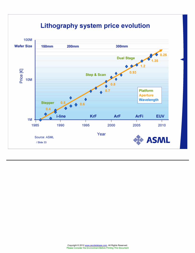
Lithography system price evolution 1M 10M 100M 1985 1990 1995 2000 2005 2010 Year Price [�] i-line 300mm 200mm 150mm KrF ArF ArFi EUV Wafer Size Stepper Platform Aperture Wavelength Step & Scan Dual Stage 0.4 0.5 0.6 0.7 0.8 0.93 1.2 0.25 Source: ASML 1.35
Copyright © 2012 www.secdatabase.com. All Rights Reserved.Please Consider the Environment Before Printing This Document
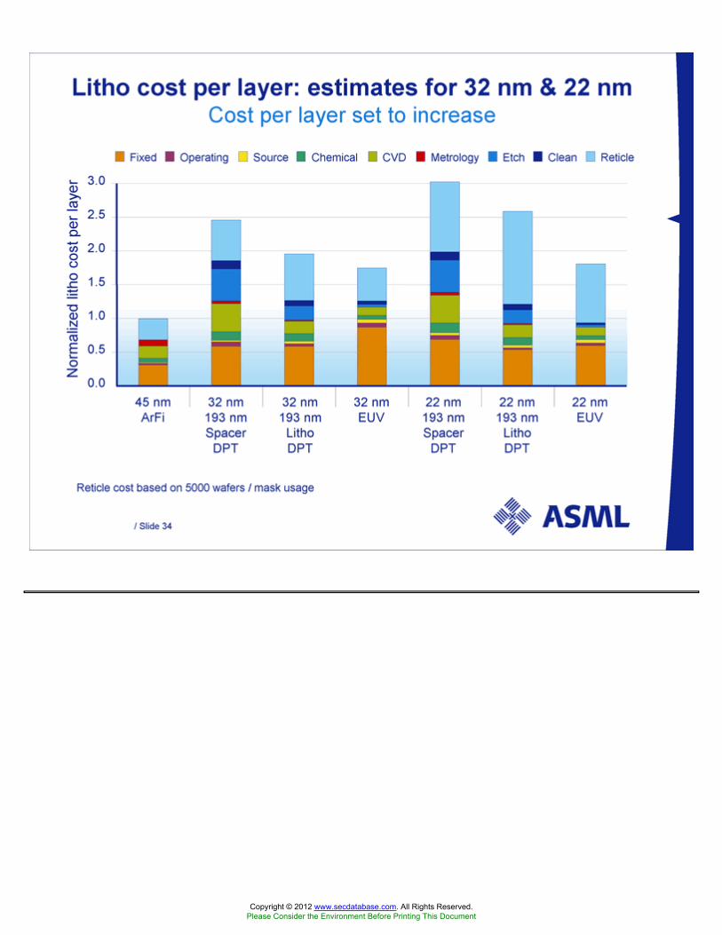
Litho cost per layer: estimates for 32 nm & 22 nm Cost per layer set to increase Reticle cost based on 5000 wafers / mask usage Fixed Operating Source Chemical CVD Metrology Etch Clean Reticle 0.0 0.5 1.0 1.5 2.0 2.5 3.0 32 nm 193 nm Spacer DPT Normalized litho cost per layer 45 nm ArFi 32 nm 193 nm Litho DPT 22 nm 193 nm Spacer DPT 32 nm EUV 22 nm 193 nm Litho DPT 22 nm EUV
Copyright © 2012 www.secdatabase.com. All Rights Reserved.Please Consider the Environment Before Printing This Document

ASML system throughput improvement drives CoO 0 40 80 120 160 200 1985 1990 1995 2000 2005 2010 g-line i-Line KrF ArF ArFi Wavelength Wafer size Year of introduction ATP throughput [Wafers Per Hour] 200 mm stepper 150 mm stepper 200 mm scanner 300 mm TWINSCAN scanner XT:1900Gi 300 mm Next TWINSCAN 150 mm 200 mm 300 mm
Copyright © 2012 www.secdatabase.com. All Rights Reserved.Please Consider the Environment Before Printing This Document

Evolution in 300mm litho costs per layer * Including chemicals, track, mask, deposition etc. Litho costs per single layer* [�] 2003 2004 2005 2006 2007 2008 2009 2010 Year 1 10 100 ~10% average cost reduction / year 0.93 NA 1.35 NA 1.2 NA ArFi ArF KrF i-Line 0.85 NA 0.8 NA 0.65 NA
Copyright © 2012 www.secdatabase.com. All Rights Reserved.Please Consider the Environment Before Printing This Document
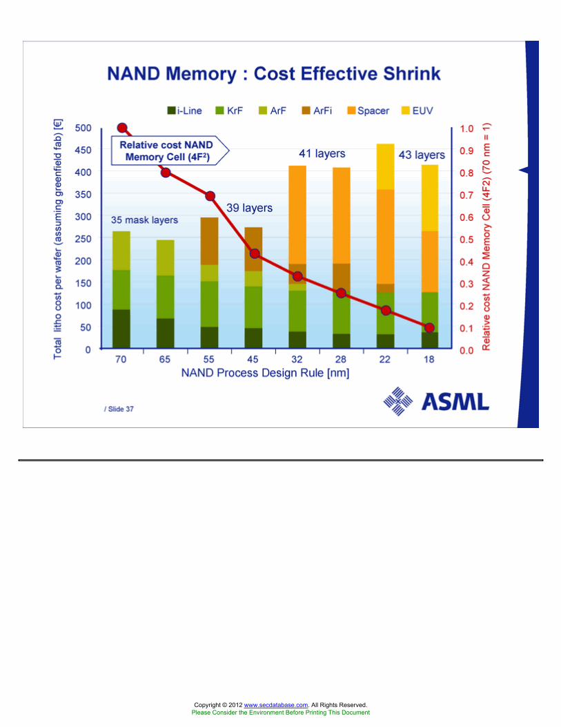
NAND Memory : Cost Effective Shrink 0 50 100 150 200 250 300 350 400 450 500 70 65 55 45 32 28 22 18 0.0 0.1 0.2 0.3 0.4 0.5 0.6 0.7 0.8 0.9 1.0 i-Line KrF ArF ArFi Spacer EUV NAND Process Design Rule [nm] Total litho cost per wafer (assuming greenfield fab) [�] 35 mask layers 39 layers 41 layers 43 layers Relative cost NAND Memory Cell (4F2) Relative cost NAND Memory Cell (4F2) (70 nm = 1)
Copyright © 2012 www.secdatabase.com. All Rights Reserved.Please Consider the Environment Before Printing This Document

Strong DPT EUV DFM supported low k1, light DPT EUV Year of Production Start* Resolution, "Shrink" [nm] 100 80 60 Logic NAND Flash DRAM 30 20 50 *Process development 1.5 ~ 2 years in advance (updated 12/07) 200 Double patterning will bridge the gap between single exposure 193 nm immersion and EUV AT:1200 XT:1400 XT:1900i Next EUV ASML product Introduction 40 XT:1700i Jan - 02 Jan - 03 Jan - 04 Jan - 05 Jan - 06 Jan - 07 Jan - 08 Jan - 09 Jan - 10 Jan - 11 Jan - 12 Jan - 13 Jan - 14
Copyright © 2012 www.secdatabase.com. All Rights Reserved.Please Consider the Environment Before Printing This Document

Commitment
Copyright © 2012 www.secdatabase.com. All Rights Reserved.Please Consider the Environment Before Printing This Document
FBR Capital Markets 12th Annual Spring Investor Conference ASML continues to execute its leadership strategy Craig De Young VP Investor Relations and Corporate Communications New York City - May 28-29, 2008
Copyright © 2012 www.secdatabase.com. All Rights Reserved.Please Consider the Environment Before Printing This Document
Safe Harbor Forward Looking Statements "Safe Harbor" Statement under the US Private Securities Litigation Reform Act of 1995: the matters discussed in this document may include forward-looking statements, including statements made about our outlook, realization of backlog, IC unit demand, financial results, average sales price, gross margin and expenses. These forward looking statements are subject to risks and uncertainties including, but not limited to: economic conditions, product demand and semiconductor equipment industry capacity, worldwide demand and manufacturing capacity utilization for semiconductors (the principal product of our customer base), competitive products and pricing, manufacturing efficiencies, new product development and customer acceptance of new products, ability to enforce patents and protect intellectual property rights, the outcome of intellectual property litigation, availability of raw materials and critical manufacturing equipment, trade environment, changes in exchange rates and other risks indicated in the risk factors included in ASML's Annual Report on Form 20-F and other filings with the US Securities and Exchange Commission.
Copyright © 2012 www.secdatabase.com. All Rights Reserved.Please Consider the Environment Before Printing This Document

ASML - the world's largest supplier of lithography equipment Source: Semi & ASML Leadership in immersion for volume chip manufacturing Canon 11% ASML 65% Nikon 24% KLA Tencor ASML Tokyo Electron Lam Research Applied Materials Revenue evolution Top 5 semiconductor equipment suppliers - 2007 Market share 2007
Copyright © 2012 www.secdatabase.com. All Rights Reserved.Please Consider the Environment Before Printing This Document

The Market
Copyright © 2012 www.secdatabase.com. All Rights Reserved.Please Consider the Environment Before Printing This Document

Market in general Global economic weakness drives slowdown of overall 2008 semiconductor capex forecast by analysts and customers DRAM makers reduce capacity plan and are driving prices of memory chips up Two Flash makers delayed new factories, flash prices continue to be weak Customer factory utilization rates remain high Independent market researchers are uncertain about semiconductor growth rates
Copyright © 2012 www.secdatabase.com. All Rights Reserved.Please Consider the Environment Before Printing This Document

ASML affected by changing market environment Recent capacity delay decisions by one DRAM factory expansion and two new Flash factories impact Q1 orders and '08 outlook Rationalization efforts amongst Taiwanese DRAM players ongoing Overall economic uncertainty causing caution at Foundries Demand for immersion tools remain strong
Copyright © 2012 www.secdatabase.com. All Rights Reserved.Please Consider the Environment Before Printing This Document

ASML's assessment of 2008 worldwide lithography demand March 2008 ASML shipped 260 machines in 2007 with ASP of � 12.9 million ASML expects market share gains and substantial ASP growth in 2008 Numbers include new and used equipment Source: ASML April 2008 April 2008
Copyright © 2012 www.secdatabase.com. All Rights Reserved.Please Consider the Environment Before Printing This Document
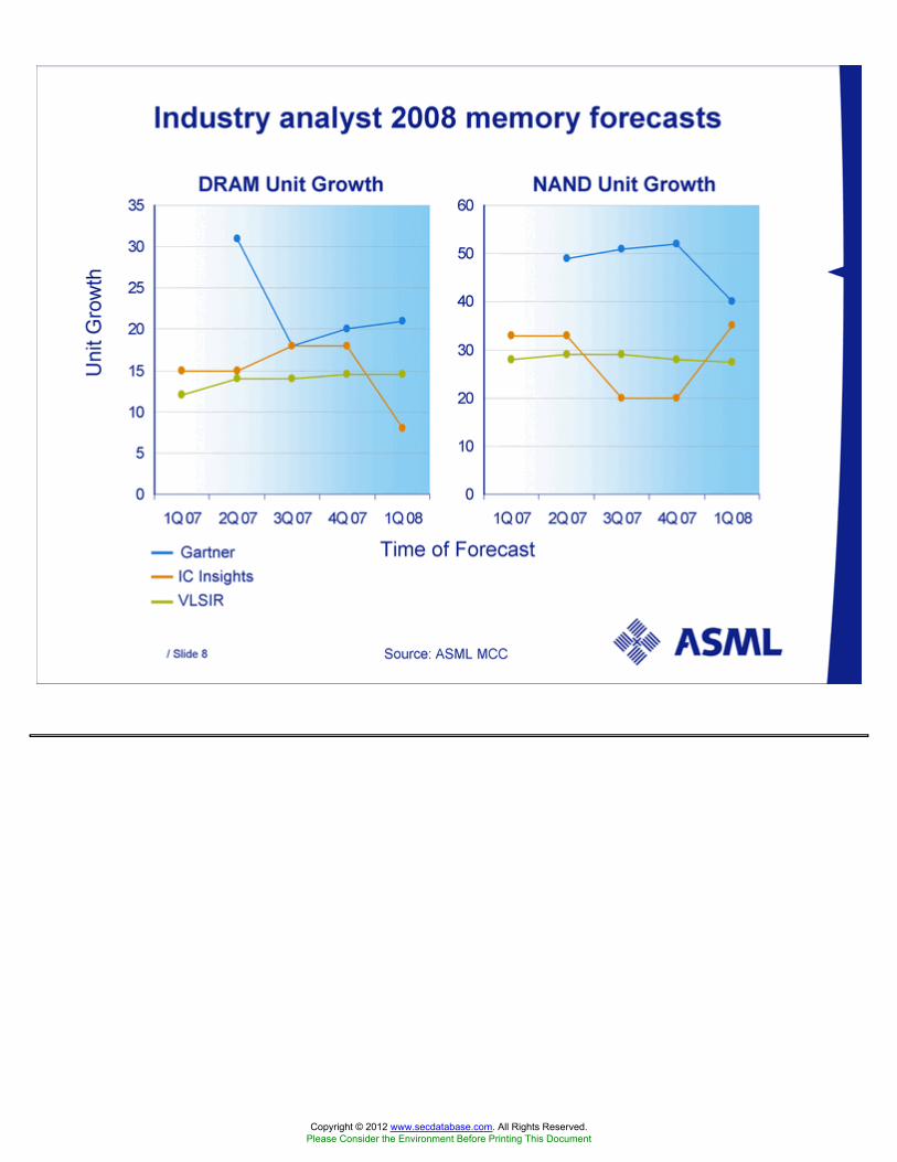
Industry analyst 2008 memory forecasts Source: ASML MCC Unit Growth Time of Forecast DRAM Unit Growth NAND Unit Growth Gartner IC Insights VLSIR
Copyright © 2012 www.secdatabase.com. All Rights Reserved.Please Consider the Environment Before Printing This Document

Recent positive DRAM Developments Pricing rising/stabilizing Samsung raises capex $1 billion Micron/Nanya plan to convert Nanya Fab 2 from 200mm to 300mm state of the art DRAM processing ProMOS signed a 54nm technology license agreement with Hynix. ProMOS expects to pilot 54nm production in late 2008/early 2009 Elpida Memory Inc. forms a tie-up with Qimonda for the development and fabrication of next-generation DRAM by jointly developing 40-nanometer processing technology; they also aim to co-develop 30nm processing technology
Copyright © 2012 www.secdatabase.com. All Rights Reserved.Please Consider the Environment Before Printing This Document

2008 : Foundry 65nm ramp, MPU 45nm, 5xnm DRAM (1Gb), 4xnm NAND (32Gb), 3xnm process development with DPT 10 12 Resolution, "Shrink" (nm) 200 100 80 60 40 Logic DRAM NAND 11 07 09 08 04 06 05 01 03 02 00 ASML Product Introduction XT:1400 XT:1700i AT:1200 AT:850 Double Patterning XT:1900i EUV Immersion EUV DPT
Copyright © 2012 www.secdatabase.com. All Rights Reserved.Please Consider the Environment Before Printing This Document
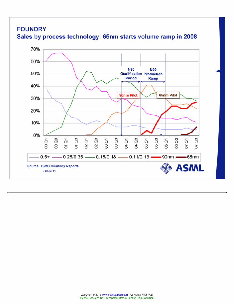
65nm Pilot 90nm Pilot N90 Qualification Period N90 Production Ramp Source: TSMC Quarterly Reports FOUNDRY Sales by process technology: 65nm starts volume ramp in 2008
Copyright © 2012 www.secdatabase.com. All Rights Reserved.Please Consider the Environment Before Printing This Document

FOUNDRY Bi-annual capacity increase pattern* suggests improved 2H/08 Foundry utilization triggers ASML litho equipment purchases Source: ASML MCC (SAP-IFP update 12/07) * Utilization seems to drop mainly as result of capacity additions. If pattern holds, foundry will likely add capacity again in 2008. This is not a forecast. 2002 2003 2004 2005 2006 2007 2008 TWINSCAN Add Point
Copyright © 2012 www.secdatabase.com. All Rights Reserved.Please Consider the Environment Before Printing This Document

ASML technology leader
Copyright © 2012 www.secdatabase.com. All Rights Reserved.Please Consider the Environment Before Printing This Document

Source: ASML Immersion technology used in volume production for 55 nm resolution and beyond ASML immersion installed base 86 tools 25 in the US 53 in ASIA, (16 in Japan) 8 in Europe
Copyright © 2012 www.secdatabase.com. All Rights Reserved.Please Consider the Environment Before Printing This Document

Technology drives ASML product acceptance Japanese memory manufacturers embracing ASML Immersion solutions ASML KrF is showing clear advantage for CCD CMOS Image sensor application in Japan. Key device at Japanese plasma TV manufacturer to be made using ASML Immersion systems ASML Immersion systems selected by a Japanese manufacturer for microprocessor production
Copyright © 2012 www.secdatabase.com. All Rights Reserved.Please Consider the Environment Before Printing This Document

Next generation lithography: EUV Prototypes shipped in 2006 Five Pilot production machines to ship 2010 Albany Leuven
Copyright © 2012 www.secdatabase.com. All Rights Reserved.Please Consider the Environment Before Printing This Document

/ Slide 17 EUVL Roadmap down to 11 nm support 22 nm and 16 nm node with a single projection system same projection system, enhanced off-axis illumination implementation volume production Res 11 nm 16 nm 22 nm 27 nm 2014 2015 2013 2010 2011 2012 0.32 NA +off axis illumination 0.32 NA, 3 nm OVL, >100 wph 0.25 NA, 4 nm OVL 0.4x NA
Copyright © 2012 www.secdatabase.com. All Rights Reserved.Please Consider the Environment Before Printing This Document

/ Slide 18 Strong DPT EUV DFM supported low k1, light DPT EUV Jan-02 Jan-03 Jan-04 Jan-05 Jan-06 Jan-07 Jan-08 Jan-09 Jan-10 Jan-11 Jan-12 Jan-13 Jan-14 Year of Production Start* Resolution, "Shrink" [nm] 100 80 60 Logic NAND Flash DRAM 30 20 50 *Process development 1.5 ~ 2 years in advance (updated 12/07) 200 Double patterning will bridge the gap between single exposure 193 nm immersion and EUV AT:1200 XT:1400 XT:1900i Next EUV ASML product Introduction 40 XT:1700i
Copyright © 2012 www.secdatabase.com. All Rights Reserved.Please Consider the Environment Before Printing This Document

/ Slide 19 Spacer DPT | SPCR 32nm Litho DPT - LELE | LDPT 32nm Litho DPT - LFLE | LDPF 32nm Double exposure | DE 38 nm SiON /HM Etch Clean Strip Film Etch Metrology Develop Expose Top coat Resist BARC SiON / SiC Hard Mask Device film Si Single exposure | SE 45nm Options to print below immersion single exposure limit Cost, complexity and cycle time *Wafer does not leave the exposure system between the two exposures *Wafer preferably does not leave the litho cell between the exposures *Wafer leaves litho cell for etch between the exposures
Copyright © 2012 www.secdatabase.com. All Rights Reserved.Please Consider the Environment Before Printing This Document
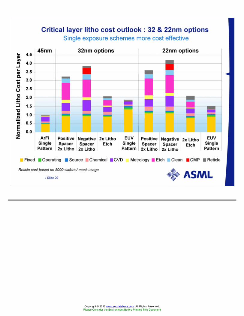
Critical layer litho cost outlook : 32 & 22nm options Single exposure schemes more cost effective 0.0 0.5 1.0 1.5 2.0 2.5 3.0 3.5 4.0 4.5 45nm 32nm options 22nm options ArFi Single Pattern Positive Spacer 2x Litho Negative Spacer 2x Litho EUV Single Pattern 2x Litho Etch Normalized Litho Cost per Layer Fixed Operating Source Chemical CVD Metrology Etch Clean CMP Reticle Reticle cost based on 5000 wafers / mask usage EUV Single Pattern 2x Litho Etch Positive Spacer 2x Litho Negative Spacer 2x Litho
Copyright © 2012 www.secdatabase.com. All Rights Reserved.Please Consider the Environment Before Printing This Document

Business summary
Copyright © 2012 www.secdatabase.com. All Rights Reserved.Please Consider the Environment Before Printing This Document

Q1 result highlights 8th consecutive quarter with sales over � 900 million Operating margin of 20.5% Cash generation � 263 million from operations Backlog at �1,167 million (booked 26 system in Q1) Shipped 14 immersion tools Record average selling price for new shipped systems of � 18.7 million
Copyright © 2012 www.secdatabase.com. All Rights Reserved.Please Consider the Environment Before Printing This Document

Total net sales M� 1,543 2,465 2,529 3,597 3,768 *2007 numbers are adjusted retrospectively with respect to the change in accounting policy.
Copyright © 2012 www.secdatabase.com. All Rights Reserved.Please Consider the Environment Before Printing This Document

Net sales breakdown in value: Q1 2008 End-use Foundry 13% Numbers have been rounded for readers' convenience Technology KrF 14% i-Line 3% ArF dry 32% USA 24% Taiwan 15% Korea 32% Japan 7% Europe 7% Sales in Units Region Other 1% ArF immersion 57% Memory 64% IDM 23% China 14%
Copyright © 2012 www.secdatabase.com. All Rights Reserved.Please Consider the Environment Before Printing This Document

Backlog lithography in value per March 30th, 2008 Total value M� 1,167 = 65 systems Technology i-Line 3% ArF immersion 57% KrF 9% ArF dry 31% Region USA 20% Taiwan 13% Korea 30% Other 6% Europe 13% Japan 9% China 9% End-use Memory 56% IDM 30% Foundry 14% Numbers have been rounded for readers' convenience
Copyright © 2012 www.secdatabase.com. All Rights Reserved.Please Consider the Environment Before Printing This Document

Outlook
Copyright © 2012 www.secdatabase.com. All Rights Reserved.Please Consider the Environment Before Printing This Document

Q2 2008 outlook ASML expects to ship 42 systems ASP for new + refurbished systems expected to be � 17.0 million Gross margin approximately 40% R&D is expected at � 130 million net of credit SG&A is expected at � 58 million Given current market weakness, we are trimming Manufacturing and SG&A variable costs for 2008 second half while keeping R&D stable
Copyright © 2012 www.secdatabase.com. All Rights Reserved.Please Consider the Environment Before Printing This Document

Outlook Order pattern translates into weaker net sales for next 2 quarters We expect gradual unit order pick-up from Q2 onwards, due to: Improvements in memory supply/demand balance Volume production ramps of 45nm node Flash memory to start in H2 2008 Foundry contribution ASML's market share gains Due to advanced technology tool mix, Q2 bookings value increase will be significant
Copyright © 2012 www.secdatabase.com. All Rights Reserved.Please Consider the Environment Before Printing This Document

Copyright © 2012 www.secdatabase.com. All Rights Reserved.Please Consider the Environment Before Printing This Document