Artigo IBM
17
RC23872 (W0602-085) February 9, 2006 Electrical Engineering IBM Research Report Prediction of Losses Caused by Roughness of Metallization in Printed-Circuit Boards A. Deutsch, C. W. Surovic, R. S. Krabbenhoft 1 , G. V. Kopcsay, B. J. Chamberlin 2 IBM Research Division Thomas J. Watson Research Center P.O. Box 218 Yorktown Heights, NY 10598 1 IBM Server Group Rochester, MN 55901 2 IBM Microelectronics Division Endicott, NY 13760 Research Division Almaden - Austin - Beijing - Haifa - India - T. J. Watson - Tokyo - Zurich LIMITED DISTRIBUTION NOTICE: This report has been submitted for publication outside of IBM and will probably be copyrighted if accepted for publication. It has been issued as a Research Report for early dissemination of its contents. In view of the transfer of copyright to the outside publisher, its distribution outside of IBM prior to publication should be limited to peer communication s and specific requests. After outside publication, requests should be filled only by reprints or legally obtained copies of the article (e.g. , payment of royalties). Copies may be requested from IBM T. J. Watson Research Center , P. O. Box 218, Yorktown Heights, NY 10598 USA (email: reports@us .ibm.com) . Some reports are availabl e on the internet at http://domino.wa tson.ibm.com/library /CyberDig.nsf/h ome .
-
Upload
william-soto -
Category
Documents
-
view
2 -
download
0
description
perda de metalização.
Transcript of Artigo IBM
7/17/2019 Artigo IBM
http://slidepdf.com/reader/full/artigo-ibm 1/17
RC23872 (W0602-085) February 9, 2006
Electrical Engineering
IBM Research Report
Prediction of Losses Caused by Roughness of Metallization in
Printed-Circuit Boards
A. Deutsch, C. W. Surovic, R. S. Krabbenhoft1,
G. V. Kopcsay, B. J. Chamberlin2
IBM Research Division
Thomas J. Watson Research Center P.O. Box 218
Yorktown Heights, NY 10598
1IBM Server Group
Rochester, MN 55901
2IBM Microelectronics Division
Endicott, NY 13760
Research Division
Almaden - Austin - Beijing - Haifa - India - T. J. Watson - Tokyo - Zurich
LIMITED DISTRIBUTION NOTICE: This report has been submitted for publication outside of IBM and will probably be copyrighted if accepted for publication. It has been issued as a Research
Report for early dissemination of its contents. In view of the transfer of copyright to the outside publisher, its distribution outside of IBM prior to publication should be limited to peer communications and specific
requests. After outside publication, requests should be filled only by reprints or legally obtained copies of the article (e.g., payment of royalties). Copies may be requested from IBM T. J. Watson Research Center , P.
O. Box 218, Yorktown Heights, NY 10598 USA (email: reports@us .ibm.com) . Some reports are availabl e on the internet athttp://domino.watson.ibm.com/library/CyberDig.nsf/home.
7/17/2019 Artigo IBM
http://slidepdf.com/reader/full/artigo-ibm 2/17
7/17/2019 Artigo IBM
http://slidepdf.com/reader/full/artigo-ibm 3/17
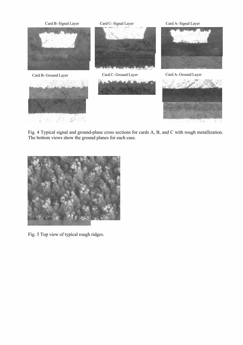
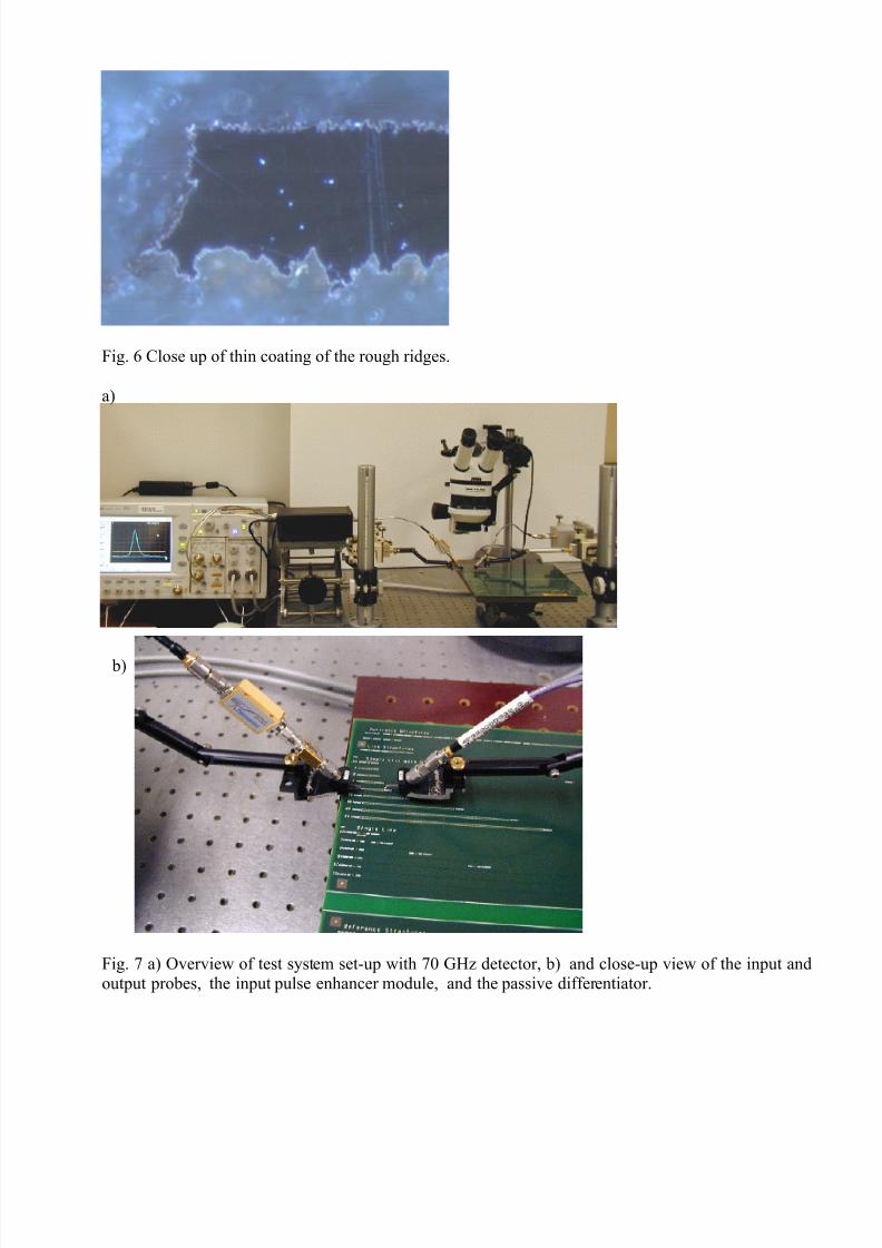
Notice the ridges on the side of the signal lines in addition to the top and the very high irregularity on the ground plane for
card A in Fig. 4. Fig. 6 shows a very close view of the ridge tips. It can be seen that micro-nodules are electroplated that
could be in size from 0.1 to 1 µm to promote adhesion. This increases surface area without adding to the overall topography.
In addition, the side of the ridges and the conductor outline could have a thin layer of an organo-metallic compound. This will
differ depending on whether the manufacturer used standard, reverse, or dual treatment. It is explained in [5-6] that standard
treatment would be applied to the toothed, or non-drum side of the copper foil and was generally used on the three cardsshown here. Fig. 6 shows a typical view of this alloy layer. The metals that are used can have resistivity that is more than an
order of magnitude higher than for copper.
Eight cross sections were taken at various positions along the lines and one parallel to the length of the lines. It was foundthat for the card A, the low profile, LP, case, had the ridge height in the range of 2.5-5 µm, and for the rough case, 7.5-10 µm.
For card B, the rough signal layer had ridges that were on the average 7.5 µm tall and 8 µm wide. The ground layer had 5.5
µm heights and 7.4 µm widths. For card C, the signal layer had heights of 5.3 µm and widths of 10.3 µm and for the ground
layer, heights of 7.5 µm and widths of 8.6 µm. For typical copper resitivity of 2 µΩcm, skin-depth is in the range of 1.03 to
0.36 µm for 5 GHz to 40 GHz. This means, that the dimension of the ridges are larger than the skin-depth and the current will
follow the contour of the ridges and increase the effective resistance and inductance and slow-down the wave propagation.
The higher resistivity coating on the surface of the ridges will exacerbate this effect. Moreover, the irregularity of the random
ridges could generate some non-TEM components of the field longitudinally and further affect the wave propagation.
DC Analysis
The resistance, capacitance, and cross sectional dimensions were analyzed for all six cards in order to ensure that similar
conditions were used for comparison and the data is shown in the table below. Given the fact that these parts came from three
different manufacturers, it is believed that the results were quite close. Resistivity was obtained from cross sectional
dimensions and four-point resistance measurements. Line capacitance and dielectric constants'
r ε were obtained at 1 MHz.
'
r ε was obtained from measuring the capacitance of a 12.7-mm (500-mil) diameter circular plate placed on the signal layer. It
is observed that the effective DC resistivity increased only in the range of 0.05 – 0.6%. The effective dielectric constantincreased by 2.4-4.3% at 1 MHz. Card B had the largest area difference between smooth and rough cards, namely 8.6%. The
other two had very similar dimensions with ∆Area = 1.9-4.8%. The resultant line capacitance changed by only 1.2-3.1% dueto roughness. If the cross section is slightly smaller and the dielectric constant is slightly higher, the resultant capacitance will
not change too much unless the effect of roughness is significant. This did not seem to be the case. In all cases, an average line
cross section was assumed through the middle of the rough ridges. In summary, the Table shows that the effect of roughness
on effective DC resistivity and low-frequency effective dielectric constant are very small. This was also confirmed by
measuring the characteristic impedance in TDR, Z o. The impedance values for rough and smooth cards were within 1%.
Extraction of Total Loss
It was shown in [3], that a short-pulse propagation time-domain technique combined with signal processing and iterativefitting and modeling can successfully extract the total loss for representative stripline interconnects over the range 10 KHz to
50 GHz. It relies on a carefully built representative test vehicle that minimizes the interface discontinuities but retains all the
key processing steps of an actual multi-layer card. High-bandwidth time-domain instrumentation and accessories are usedsuch as the Agilent 86100B sampling oscilloscope with an 86118A, 70 GHz, detector unit connected through 65 GHz cables
and coaxial probes (such as 67A from GGB Industries). In addition, the Picoseconds Pulse Labs 4022 TDT Source Pulse
Enhancer and 5206 Differentiator allow the generation of 11 ps risetime step and 20 ps wide pulse excitations. Figs. 7a and b
show an overall view of the measurement set-up and a close-up of the input and output coaxial probing. The 20-ps wide short
pulse is launched on two identical lines of different lengths. Signal processing of the digitized, propagated pulses consists ofrectangular time-windowing to eliminate reflections from pads, vias, probes, and the Fourier transformation into frequency-
domain data. The two Fourier transforms are ratioed and from the ratio of the amplitudes and difference in phase, the
attenuation, α (f), and phase constant, β (f), are obtained. This is achieved without any calibration or de-embedding as used innetwork-analyzer based techniques. In the ratio operation, the effects of discontinuities will cancel out. Accurate sample cross
sectioning is performed at many locations. Based on this, R(f) and L(f) per unit length can be calculated with a field solversuch as CZ2D [4]. C(f) and G(f) can also be obtained with the same field solver if the complex permittivity is known. An
initial starting set of values for the loss tangent at a few frequencies is given to the solver and the dielectric constant'
r ε at 1
MHz. The solver has a built-in Debye model for ε( f ) that guarantees causal response. Once the initial R(f), L(f), C(f), and G(f)
are obtained, the calculated and measured attenuation and phase constant, α( f ) and β( f ), are compared. A few iterations are
made on the initial guess to improve the fit. The 1 MHz'
r ε is obtained from the capacitance measurement of the large circular
plate placed on the signal layer. A few additional low frequency tanδ values are added to the initial starting values. These are
obtained from LCR-meter based tanδ measurements of the plate in the 10 KHz to 1 MHz range. Having C(f), G(f), C1MHz, and
7/17/2019 Artigo IBM
http://slidepdf.com/reader/full/artigo-ibm 4/17
'
r ε 1MHz allows the broadband extraction of'
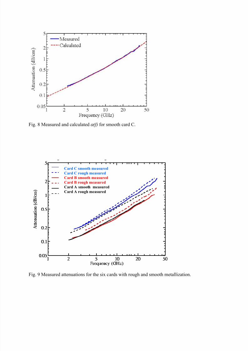
r ε (f ) and tanδ(f). Fig. 8 shows a typical comparison of measured and calculated
attenuation for the smooth card C. In this case the measurement bandwidth was 2.2 GHz to 38 GHz and the Debye model
extrapolated the data over the 10 KHz to 50 GHz range. Fig. 9 shows the measured attenuations for all six card cases.
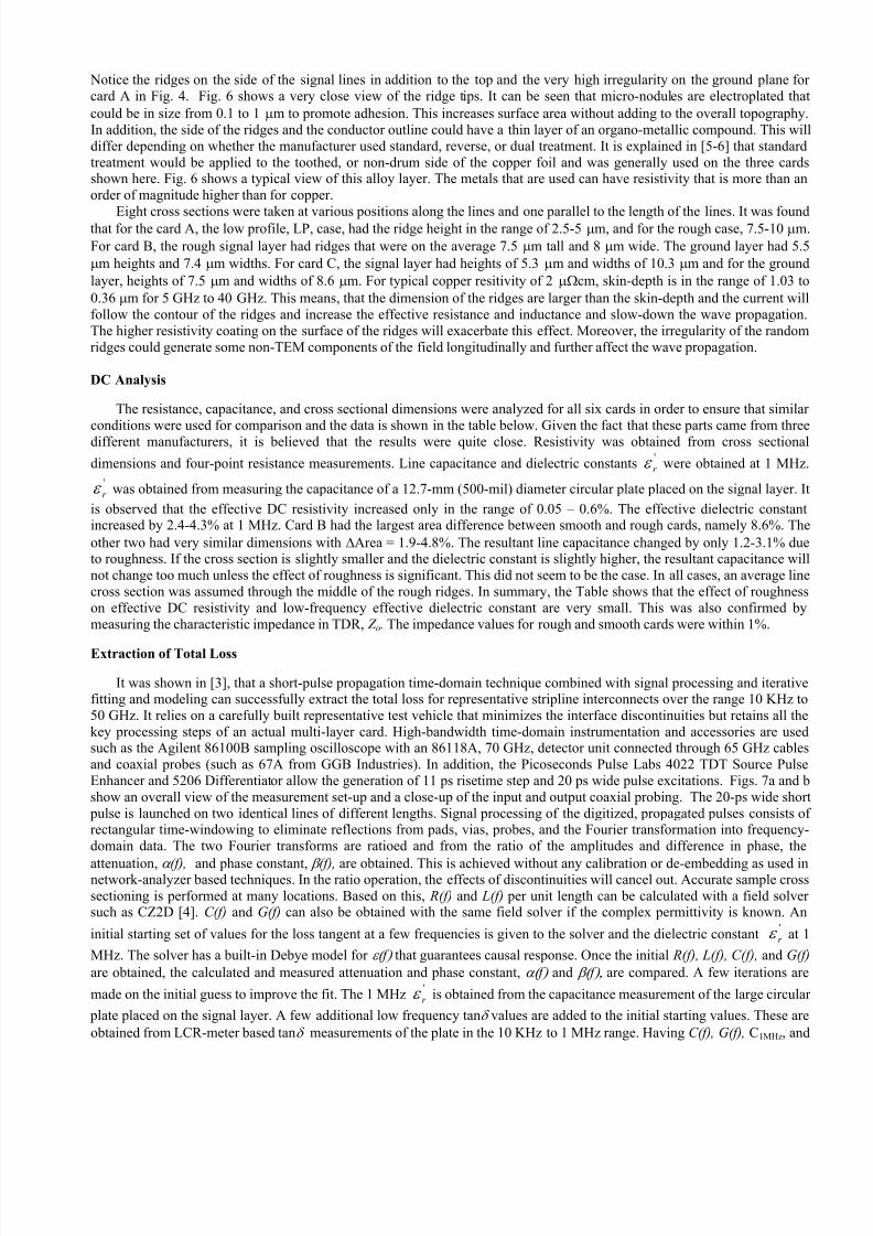
It has been proposed to use a Debye model to represent the slowly varying )(' f r ε and tanδ(f) properties of most printed-
circuit board insulator materials. It ensures causality for ε( f ) and is a good representation for the polarization-damping basedlosses. The analytic function below
(1)
can be calculated with a small number of poles. A typical representation for a good broadband model might have 30 poles
over the range 10 KHz to 1000 GHz. Ten values could be specified and interpolation and piecewise linear expansion with
respect to log(f) can be made to consistently determine both )(' f r ε and tanδ (f) over the desired frequency range. Fig. 10
shows simulation results for a 38 cm long line and 6 Gbps transmission for four conditions. Simulation was made with ten
initial tanδ values in the range of 10 GHz to 50 GHz, two values, namely at 1 MHz and 50 GHz, constant'
r ε and tanδ , and
constant values without using a Debye model. It was found that the differences in amplitude were -28.3 mV, -8.5 mV, and
+6.9 mV compared to the ten-value case with amplitude of 561 mV, respectively. The delay differences were -16 ps, -25 ps,and +70 ps , respectively. The accuracy of the model increases with the number of specified input values, however, all Debye-
based models are much closer to each other and to measurements than when causality is not respected. For constant '
r ε and
tanδ , G = ω Ctanδ expression is used with C at 1 MHz and this cannot provide consistency of complex ε ( f ) and results inlarge simulation errors.
Effect of Surface Roughness
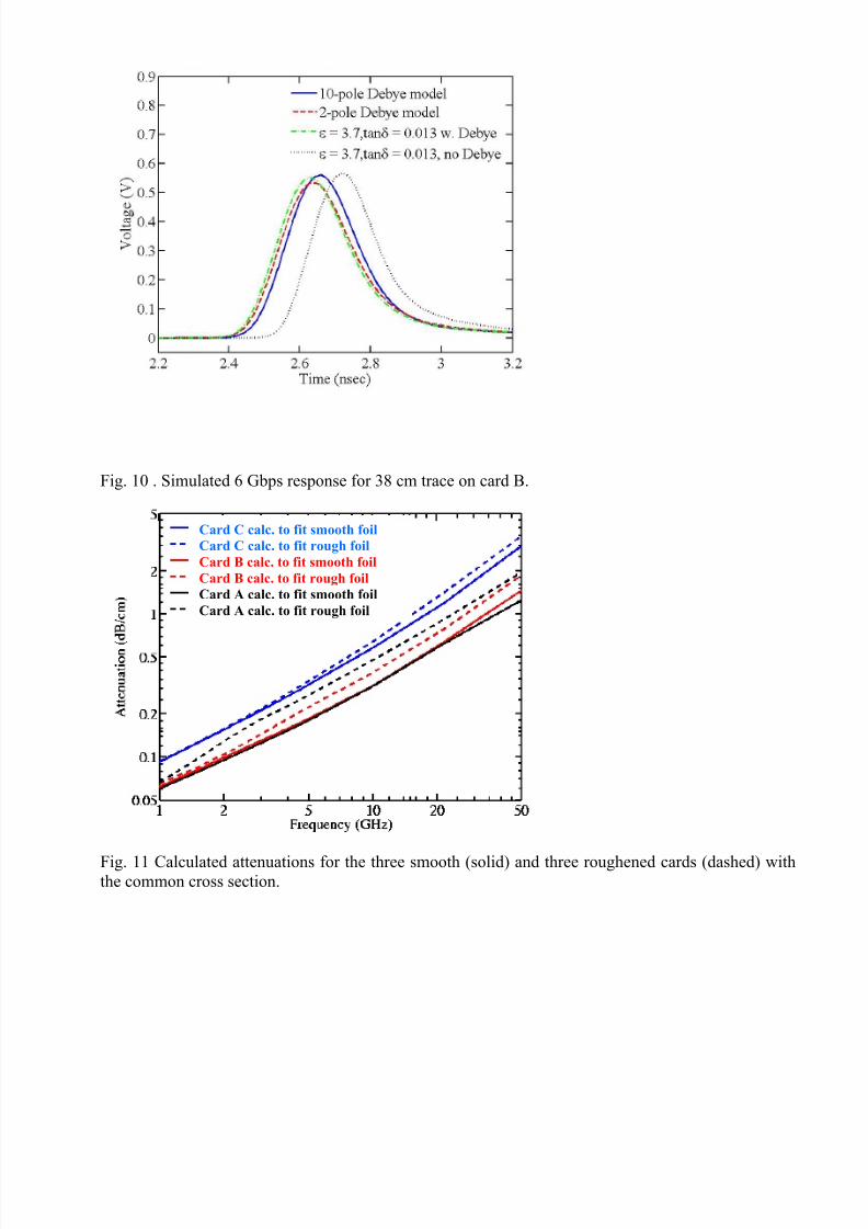
In order to eliminate the effect of slight differences in cross section, resistivity, and dielectric constants, a common cross
section with a trapezoidal shape of width 91.9 / 109 µm (3.62 / 4.29 mil) or effective 100.5 µm (3.955 mil) and thickness of
32.0 µm (1.26 mil) was used for all three materials. The dielectric heights were h1 = h2 = 114.0 µm (4.49 mil). In all three
cases, the conditions for R(f), L(f), C(f), and G(f) calculations were such that the fit was either made to the total loss for the
smooth cards or the total loss for the roughened cards, but the cross section was the same. The'
r ε 1MHz and ρ DC that were used
were extracted from measurements of the six actual cards of this study. Fig. 11 then shows the resultant six attenuations. The
solid traces correspond to the smooth cards. The low-loss materials A and B have a substantial increase in total loss due to
roughness. At 5 GHz, A and B cards have an increase in attenuation of 49.8% and 20.3%, respectively. At 10 GHz, the
increase is 53.4% and 23.6%. Material A with roughened metallization produces a total interconnect loss that is very close tothe loss of card C which is a standard material in use today. All the advantages of lower tan δ are overwhelmed by the losses
due to roughness. Material C in fact has the least increase due to the ridges, namely at 5 GHz, only 5.5% increase, and at 10GHz, 10.6%. It is possible that the newer materials require a more aggressive roughening process. Fig. 12 plots the differences
in attenuation caused by roughness.
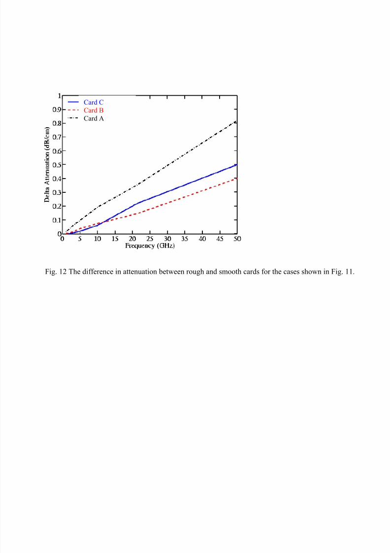
The values shown in Fig. 11 for the roughened cards were calculated by assuming an average cross section through the
rough ridges. What this implies is that when extracting the effective'
r ε (f) and tanδ (f), the effect of roughness which is an
additional resistive loss, gets attributed to dielectric loss. This is because the actual topography of the ridges is not accounted
for. As a result, the error in the extracted tanδ is quite large as shown in Fig. 13. This issue has also been highlighted in [7]and attempts have been made to find analytical techniques fitted to measurements to alleviate this error. Fig. 14 shows the
extracted dielectric constants for the smooth cards.
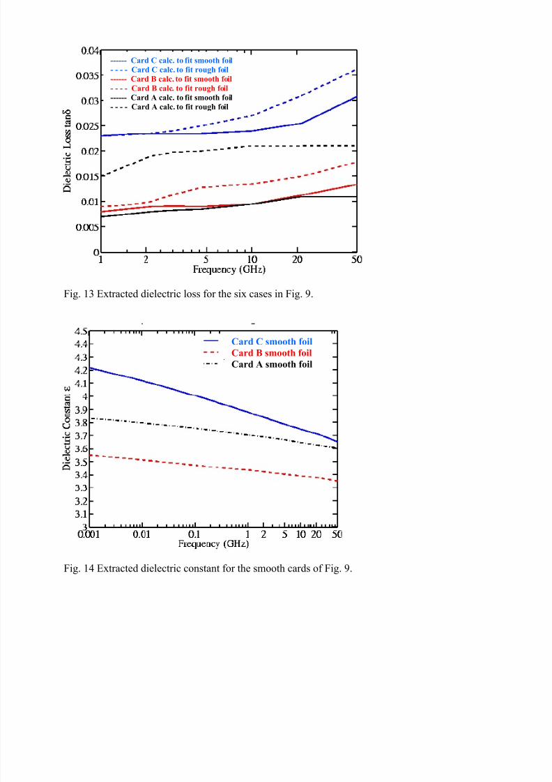
Modeling the Effect of Roughness
Including the actual profile of the ridges shown in Fig. 5 in any full-wave electromagnetic field solver can be extremely
costly in the number of unknowns and run time. Attempts have been made to use stochastic techniques for the calculation ofcapacitance [8] and effective conductivity [9] but complete broadband causal model generation has not been attained. In this
study, an attempt was made to continue using the two-dimensional field solver that was used for the smooth card analyses. An
equivalent cross section is shown in Fig. 15 for card B. 7.5 µm tall rectangles with 8 µm and 5 µm widths and 3 µm
separations represented the ridges. Each rectangle had a 1 µm shell of material with resistivity of ρ = 15 µΩcm. The ridges on
the ground layer were represented by a thin, 5.5 µm, layer with ρ = 15 µΩcm. The extraction was then performed for C(f) and
G(f) by using the tanδ values obtained for the smooth card. For the case of card C, the equivalent cross section had uniform
ridges with widths of 10 µm, heights of 5.5 µm, and resistivity of 2.086 µΩcm. The ground ridges were represented by a 7.5
µm thick layer with resistivity of ρ = 50 µΩcm. This type of a simplification can only be achieved if both the smooth and
roughened versions of the same build are available. This can, however, alleviate very costly computations and provide fairly
∑ ++= ∞
i i
i jωτ
ε ε ω ε 1)(
7/17/2019 Artigo IBM
http://slidepdf.com/reader/full/artigo-ibm 5/17
accurate, causal, predictive broadband models for system performance assessment. Notice that the 2D model will differ for
each material and build condition. The attenuation differences are shown in Fig. 16 for card A and compared with
measurements. For the rough case, results are compared for the cases where an average cross section through the middle of theridges is assumed (no ridges), the case where only signal ridges are included in the modeling ( signal ridges), and the case
where both signal ridges and a high resistivity thin layer is included on the ground plane. The effect of the ridges on the
ground plane is not large but it can add error in the prediction and should not be ignored. The magnitude of this error is shown
in Fig. 16. Including all effects with this type of 2D modeling can provide a fairly good model over a wide frequency range
and the model is guaranteed to be causal.
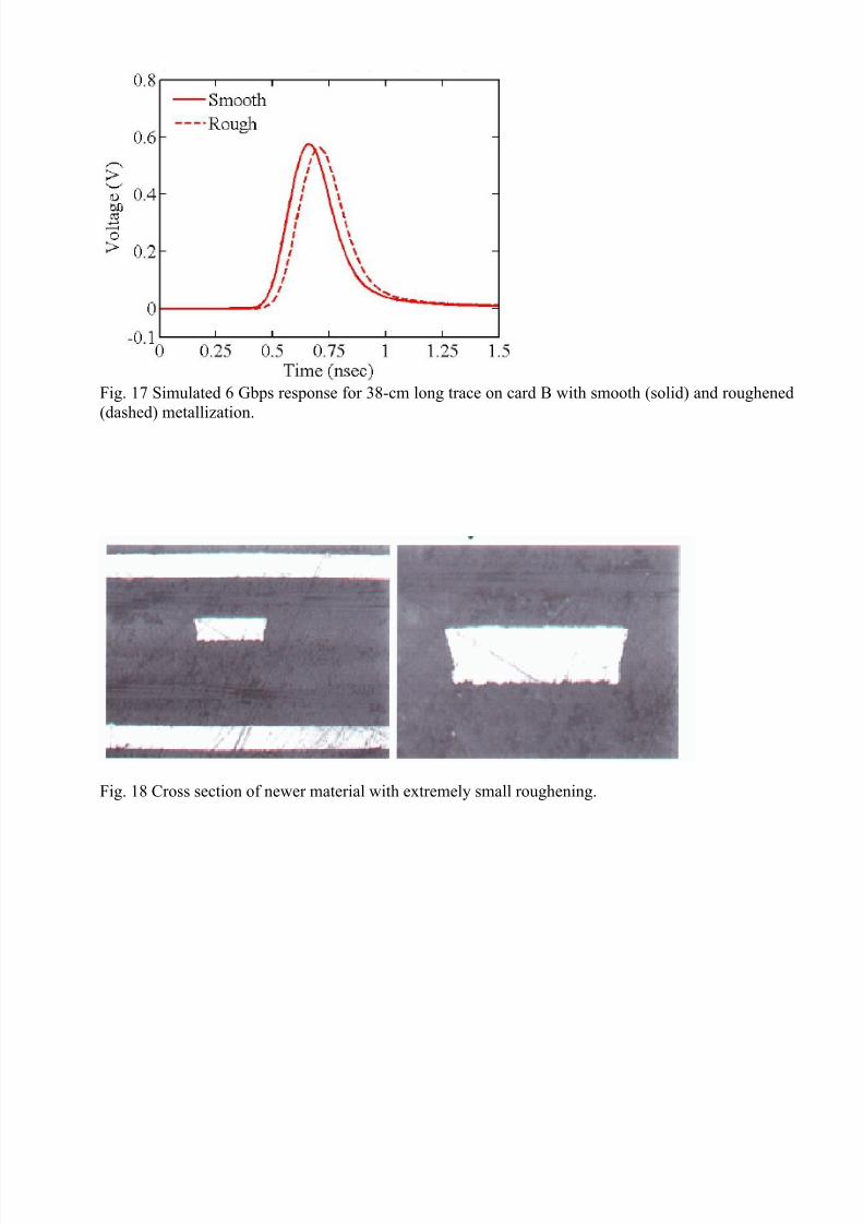
Simulations were also performed for two representative data-rates, namely 3 Gbps and 6 Gbps, with and withoutroughness-induced loss. 333 ps and 166 ps wide pulses were transmitted on 76.2 cm and 38 cm long lines, respectively, with
the card B wiring and the common cross section described earlier for Fig. 11. For the 3 Gbps case, the loss in useable lengthwas 2.12 cm (2.8%), the loss in amplitude was 1.8%, and the delay increase was 95.6 ps or 1.9%. In the case of 6 Gbps, as
shown in Fig. 17, the loss in useable length was 4 cm or 10.5%, the increase in delay was 44 ps or 1.8%, and the decrease in
signal amplitude was 17.5%.
Conclusions
It has been shown that resistive losses caused by the roughening of metallization in printed-circuit board wiring can be
quite significant. The increase of total loss ranged from 5.5% to 49.5%, even at 5 GHz. The use of roughness to promote
adhesion can cancel the beneficial low dielectric loss characteristics of newly developed card insulators and manufacturersneed to thrive to eliminate the rough ridges. The effect on signal integrity was shown to increase with frequency and could
curtail the delivery of high-performance systems or increase system complexity and cost.
One of the most significant finding of the study was that this effect will be quite different in characteristic depending onmaterial used by card manufacturer and treatment employed by supplier of metal foil. The rough ridge profile could even
differ on the ground plane layer from the signal line layer within the same card cross section. The coating of the lines and the
composition of the micro-nodules is not generally released or known by vendors and the effective resistivity can besignificantly higher than for copper metallization. The resultant composite cross section cannot be predicted. Moreover,
accurate three-dimensional modeling is prohibitive in computation cost. Even faster stochastic modeling approaches require
cross sectional information which is hard to obtain. This is then the second significant finding of the paper, namely that any
modeling technique requires some amount of fitting to actual hardware. Because of this, a practical approach that circumvents
costly analyses was outlined in this paper. It relies on the availability of a smooth version of the card build for each material
considered. This allows the use of fast, two-dimensional modeling techniques for generating causal, broadband, predictivemodels for simulation. The implicit assumption is that the two card constructions maintain the same insulator properties. Card
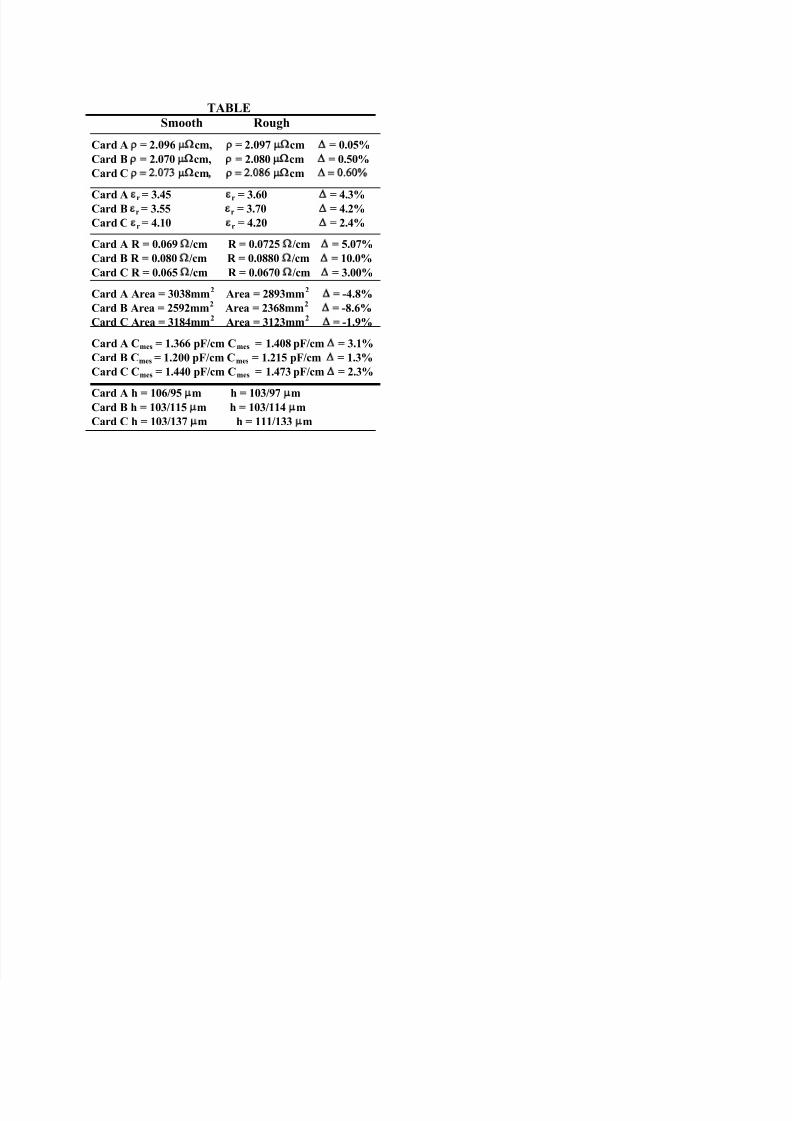
manufacturers are hard at work in developing new processing techniques that can use profile-free copper as was recentlyshown in [10] and one such cross section is shown in Fig. 18. The smooth material can result in lower total attenuation than
the combination of low tanδ and roughened foil. This might relax the material development requirements and afford higherdata rate transmission. Reliability testing on large multi-layer boards is still underway for these newer options.
References
[1] A. E. Ruehli and A. C. Cangellaris, “Methodology for the electrical modeling of interconnects and electronic packages”,
Proc. IEEE, vol. 89, no. 5, pp. 740-771, May 2001.[2] K. M. Cooperich, J. Morsey, A. C. Cangellaris, and A. E. Ruehli, “Physically consistent transmission line models for high-
speed interconnects in lossy dielectrics”, in Proc. IEEE 10th Topical Meeting on Electrical Performance of Electronic
Packaging, EPEP, Cambridge, MA, Oct. 29-31, 2001, pp. 247-250.[3] A. Deutsch, T-M. Winkel, G. V. Kopcsay, C. W. Surovic, B. J. Rubin, G. A. Katopis, B. J. Chamberlin, R. S. Krabbenhoft,
“Extraction of ε (f) and tanδ(f) for Printed-Circuit Board Insulators up to 30 GHz Using the Short-Pulse Propagation
Technique”, IEEE Trans. On Adv. Packg., vol. 28, no. 1, pp.4-9, Feb. 2005.[4] W. T. Weeks, L. L. Wu, M. F. McAllister, and A. Singh, “Resistive and inductive skin effect in rectangular conductors”,
IBM. J. Res. And Dev., vol. 23, pp.652-660, 1979.
[5] http://www.gould.com/cf_jtc.htm [6] B. L. Adams-Melvin, D. R. McGregor, K. H. Dietz, “eefects of Copper Foil Type and Surface Preparation on Fine LineImage Transfer in Primary Imaging of Printed Wiring Boards”, digest PC World Convention VII, pp. 1-20, Basel, Switzerland,
May 21-24, 1996.
[7] G. Brist, S. Hall, S. Clouser, T. Liang, “Non-Classical Conductor Losses Due to Copper Foil Roughness and Treatment”,digest ECWC10 Conference at APEX IPC Printed Circuits Expo and Designers Summit 2005, pp. 1-11, Feb. 22-24, 2005,
Anaheim, CA.
[8] Z. Zhu, “Efficient Integral Equation Based Algorithms for Parasitic extraction of Interconnects with Smooth or Rough
Surfaces”, PhD Thesis MIT, Aug. 2004. http://www.rle.mit.edu/cpg/people-alumni.htm.[9] L. Proekt and A. C. Cangellaris, “Investigation of the Impact of Conductor Surface Roughness on Interconnect Frequency-
Dependent Ohmic Loss”, 2003 ECTC Conference, pp.1004-1010, June 2003, New Orleans, LA.

7/17/2019 Artigo IBM
http://slidepdf.com/reader/full/artigo-ibm 6/17
[10] N. Ogawa, H. Onezeki, N. Moriike, T. Tanabe, T. Kumakura, “Profile-Free Copper Foil for High-Density Packaging
Substrates and High-Frequency Applications”, Proc. 2005 Electronic Components and Technology Conference, Las Vegas,
NV, pp.457-461.
7/17/2019 Artigo IBM
http://slidepdf.com/reader/full/artigo-ibm 7/17
Fig. 1 Calculated attenuations for complex permittivity ε (f) (solid), constant εr and tanδ=0 (dashed),
and constant εr and tanδ = 0.0133 (dot-dashed) for card B.
Skin-effect + r (f) + tan (f)
Skin effect +εr = ct, tan
δ
= 0
Skin-effect + εr = ct, tanδ
=0.0133
7/17/2019 Artigo IBM
http://slidepdf.com/reader/full/artigo-ibm 8/17
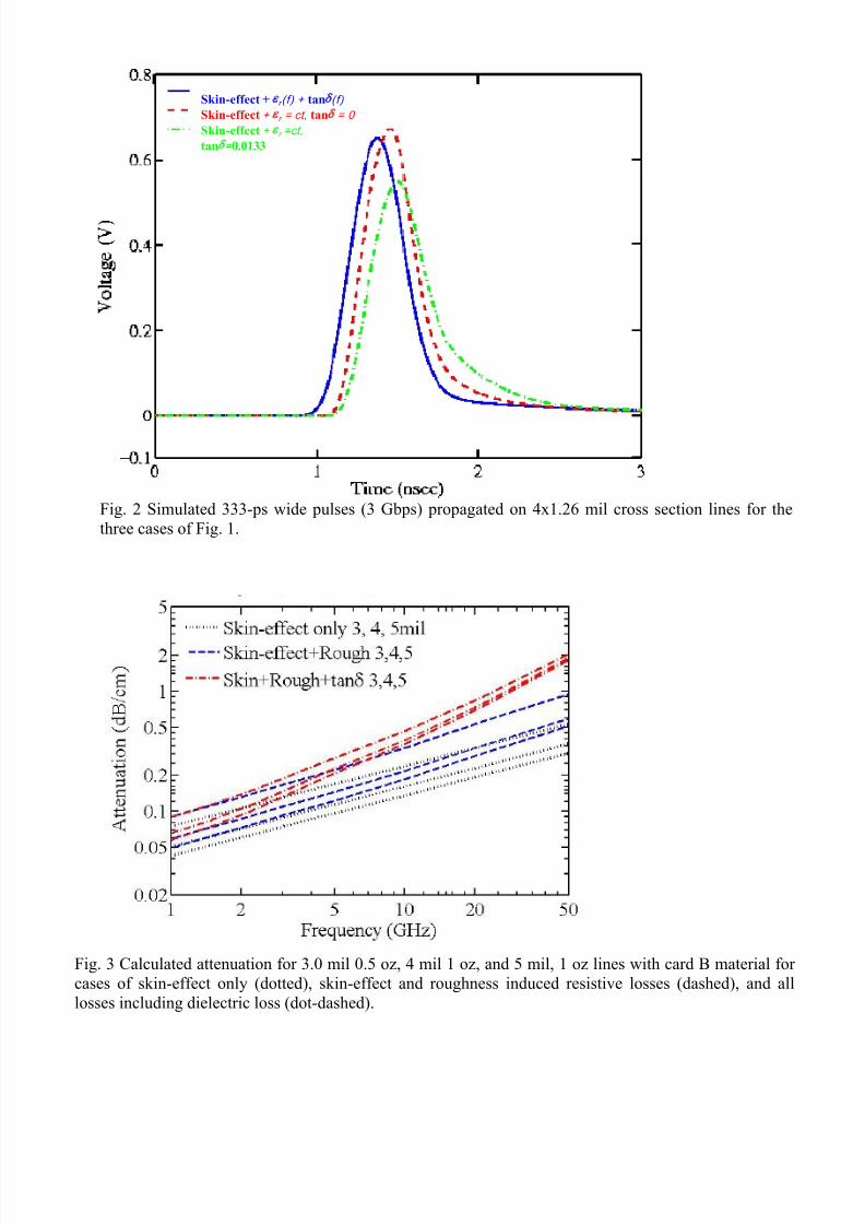
Fig. 2 Simulated 333-ps wide pulses (3 Gbps) propagated on 4x1.26 mil cross section lines for the
three cases of Fig. 1.
Fig. 3 Calculated attenuation for 3.0 mil 0.5 oz, 4 mil 1 oz, and 5 mil, 1 oz lines with card B material for
cases of skin-effect only (dotted), skin-effect and roughness induced resistive losses (dashed), and all
losses including dielectric loss (dot-dashed).
Skin-effect + r (f) + tan (f)
Skin-effect + r = ct, tan
= 0
Skin-effect + r =ct,
tan = 0.0133
7/17/2019 Artigo IBM
http://slidepdf.com/reader/full/artigo-ibm 9/17
Fig. 4 Typical signal and ground-plane cross sections for cards A, B, and C with rough metallization.The bottom views show the ground planes for each case.
Fig. 5 Top view of typical rough ridges.
Card B- Signal Layer
Card B- Ground Layer Card C- Ground Layer
Card A- Signal Layer
Card A- Ground Layer
Card C- Signal Layer
7/17/2019 Artigo IBM
http://slidepdf.com/reader/full/artigo-ibm 10/17
Fig. 6 Close up of thin coating of the rough ridges.
a)
Fig. 7 a) Overview of test system set-up with 70 GHz detector, b) and close-up view of the input andoutput probes, the input pulse enhancer module, and the passive differentiator.
b)
7/17/2019 Artigo IBM
http://slidepdf.com/reader/full/artigo-ibm 11/17
Fig. 8 Measured and calculated α (f) for smooth card C.
Fig. 9 Measured attenuations for the six cards with rough and smooth metallization.
Card C smooth measured
Card C rough measured
Card B smooth measured
Card B rough measured
Card A smooth measured
Card A rough measured
7/17/2019 Artigo IBM
http://slidepdf.com/reader/full/artigo-ibm 12/17
Fig. 10 . Simulated 6 Gbps response for 38 cm trace on card B.
Fig. 11 Calculated attenuations for the three smooth (solid) and three roughened cards (dashed) withthe common cross section.
Card C calc. to fit smooth foil
Card C calc. to fit rough foil
Card B calc. to fit smooth foil
Card B calc. to fit rough foil
Card A calc. to fit smooth foil
Card A calc. to fit rough foil
7/17/2019 Artigo IBM
http://slidepdf.com/reader/full/artigo-ibm 13/17
Fig. 12 The difference in attenuation between rough and smooth cards for the cases shown in Fig. 11.
Card C
Card B
Card A
7/17/2019 Artigo IBM
http://slidepdf.com/reader/full/artigo-ibm 14/17
Fig. 13 Extracted dielectric loss for the six cases in Fig. 9.
Fig. 14 Extracted dielectric constant for the smooth cards of Fig. 9.
------ Card C calc. to fit smooth foil
- - - - Card C calc. to fit rough foil
------ Card B calc. to fit smooth foil
- - - - Card B calc. to fit rough foil
------ Card A calc. to fit smooth foil
- - - - Card A calc. to fit rough foil
Card C smooth foil
Card B smooth foil
Card A smooth foil
7/17/2019 Artigo IBM
http://slidepdf.com/reader/full/artigo-ibm 15/17
Fig. 15 Two-dimensional model used for roughened card B.
Fig. 16 Measured and calculated attenuations using the model shown in Fig. 15.
Smooth – Measured
Rough – Measured
Calculated – no ridges
Calculated – signal ridges
Calculated – signal ridges+gnd
7/17/2019 Artigo IBM
http://slidepdf.com/reader/full/artigo-ibm 16/17
Fig. 17 Simulated 6 Gbps response for 38-cm long trace on card B with smooth (solid) and roughened
(dashed) metallization.
Fig. 18 Cross section of newer material with extremely small roughening.
7/17/2019 Artigo IBM
http://slidepdf.com/reader/full/artigo-ibm 17/17
TABLE
Smooth Rough
Card Aρ
= 2.096µΩ
cm,ρ
= 2.097µΩ
cm∆
= 0.05%
Card Bρ
= 2.070µΩ
cm,ρ
= 2.080µΩ
cm∆
= 0.50%
Card Cρ = 2.073 µΩ
cm, ρ = 2.086 µΩ
cm∆ = 0.60
Card Aε
r = 3.45ε
r = 3.60∆
= 4.3%Card B
εr = 3.55εr = 3.70
∆
= 4.2%
Card Cεr = 4.10
εr = 4.20∆
= 2.4%
Card A R = 0.069Ω
/cm R = 0.0725Ω
/cm∆
= 5.07%
Card B R = 0.080Ω
/cm R = 0.0880Ω
/cm∆
= 10.0%
Card C R = 0.065Ω
/cm R = 0.0670Ω
/cm∆
= 3.00%
Card A Area = 3038mm2 Area = 2893mm
2
∆
= -4.8%
Card B Area = 2592mm2 Area = 2368mm
2
∆
= -8.6%
Card C Area = 3184mm2 Area = 3123mm
2
∆
= -1.9%
Card A Cmes = 1.366 pF/cm Cmes = 1.408 pF/cm∆
= 3.1%
Card B Cmes = 1.200 pF/cm Cmes = 1.215 pF/cm∆
= 1.3%
Card C Cmes = 1.440 pF/cm Cmes = 1.473 pF/cm∆
= 2.3%
Card A h = 106/95µ
m h = 103/97µ
mCard B h = 103/115
µ
m h = 103/114µ
m
Card C h = 103/137µ
m h = 111/133µ
m