Array/Antenna Design in NI AWRDE - National Chiao …3gpptrend.cm.nctu.edu.tw/05....
26
ni.com/awr Array/Antenna, Beamforming Design in NI AWRDE & LabVIEW
Transcript of Array/Antenna Design in NI AWRDE - National Chiao …3gpptrend.cm.nctu.edu.tw/05....

ni.com ni.com/awr
Array/Antenna, Beamforming Design in NI AWRDE & LabVIEW

ni.com NCTU 5G Seminar
ni.com | © 2015 AWR Group of NI. All rights reserved
Antenna Array Flow
Analyst ® 3D-FEM solver
AXIEM® 3D-planar-MOM solver VSS®
RF System Simulator
ni.com NCTU 5G Seminar
ni.com | © 2015 AWR Group of NI. All rights reserved
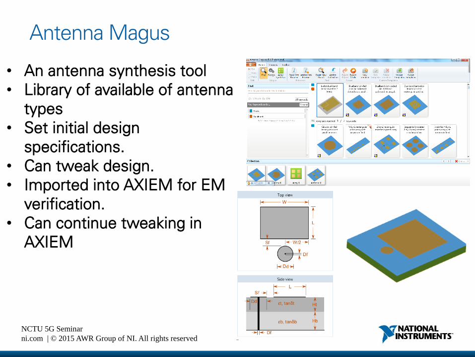
Antenna Magus
• An antenna synthesis tool • Library of available of antenna
types • Set initial design
specifications. • Can tweak design. • Imported into AXIEM for EM
verification. • Can continue tweaking in
AXIEM

ni.com NCTU 5G Seminar
ni.com | © 2015 AWR Group of NI. All rights reserved
User Interface

ni.com NCTU 5G Seminar
ni.com | © 2015 AWR Group of NI. All rights reserved
Workflow II: Designing the Antenna
• New Design>Design for Operating frequency
• Click “Design”
• Confirm/Modify “Parameter” shown in “Sketch”>Estimate Performance

ni.com NCTU 5G Seminar
ni.com | © 2015 AWR Group of NI. All rights reserved
Workflow II: Designing the Antenna
• “Tweak” parameters for tuning
• Chang representation of plot if you like

ni.com NCTU 5G Seminar
ni.com | © 2015 AWR Group of NI. All rights reserved
Workflow III: Export to AWR do EM Simulation
• Export Mode>Export and open model
ni.com NCTU 5G Seminar
ni.com | © 2015 AWR Group of NI. All rights reserved
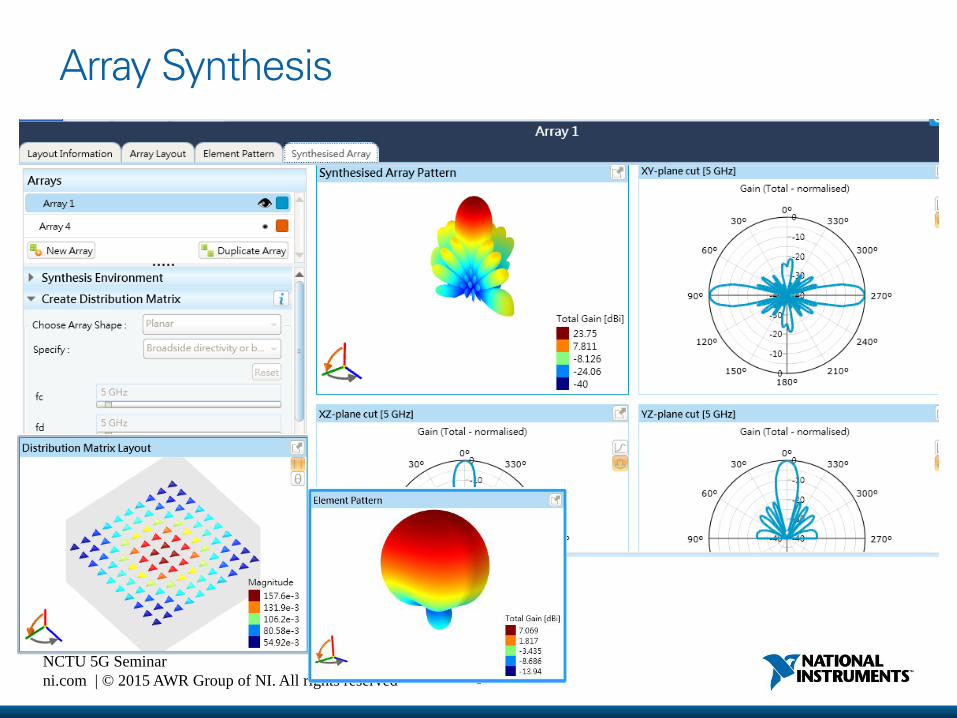
Array Synthesis

ni.com NCTU 5G Seminar
ni.com | © 2015 AWR Group of NI. All rights reserved
AWR Design Environment

ni.com NCTU 5G Seminar
ni.com | © 2015 AWR Group of NI. All rights reserved
VSS for RF System Simulation
• Develop component specifications • RF Budget and Spur Analysis • Understand impairments of the RF Link • Graphically develop custom algorithms • End-to-end simulations with modulated signals • Hardware in loop simulations

ni.com NCTU 5G Seminar
ni.com | © 2015 AWR Group of NI. All rights reserved
VSS for RF System Simulation
RF Budget Cascaded gain
Input/output IP3
Noise figure, etc.
RF Inspector Heritage tone inspector to identify the cause of
an inter-modulation product of an RF link
RF System End-to-End analysis C/N, BER, ACPR, EVM, etc.
Circuit co-simulation Matlab co-simulation
Communication Standards
WiMAX, IS2000, UWB, WCDMA 3GPP LTE, QAM, OQPSK, MPSK, GSM EDGE, DVB, 802.11a/b/g/n/ac
The most complete RF system simulation functionality in one
integrated tool

ni.com NCTU 5G Seminar
ni.com | © 2015 AWR Group of NI. All rights reserved
Typical Implementation
• Phased arrays implemented using discrete blocks • Define gain & phase offset for each element
• Specify RF link for each array element
• Allows implementation of beamforming algorithms
• Good for relatively small phased arrays

ni.com NCTU 5G Seminar
ni.com | © 2015 AWR Group of NI. All rights reserved
VSS Phased Array Configuration
• TX/RX modes • Several divider types
• Distance units • Metric
• Imperial
• Wavelength (l)
• Signal frequency • For metric/imperial
• Steering angles
• Angles of Incidence

ni.com NCTU 5G Seminar
ni.com | © 2015 AWR Group of NI. All rights reserved
Phased Array Geometry
• Standard array geometry configurations • Lattice (rectangular, triangular)
• Circular (multiple concentric circles)
• Custom configurations • Configured via X/Y locations
dx
dy
g

ni.com NCTU 5G Seminar
ni.com | © 2015 AWR Group of NI. All rights reserved
Gain Tapers
• Standard tapers: • Dolph-Chebyshev
o Side-lobe ratio (dB)
• Taylor
o Side-lobe ratio (dB)
o Near-equal side lobes
• Uniform
• User defined tapers • Gain/phase vectors for each element
ni.com NCTU 5G Seminar
ni.com | © 2015 AWR Group of NI. All rights reserved
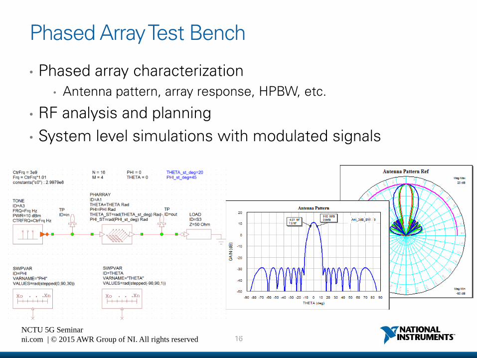
Phased Array Test Bench
• Phased array characterization • Antenna pattern, array response, HPBW, etc.
• RF analysis and planning
• System level simulations with modulated signals

ni.com NCTU 5G Seminar
ni.com | © 2015 AWR Group of NI. All rights reserved
Linear Array Example
• Linear array with 16 elements, NX=16, dx=l/2
• Dolph-Chebyshev taper, SLR=40dB
• Steering angles: q =15, f =45
• Measured HPBW = 12.8
ni.com NCTU 5G Seminar
ni.com | © 2015 AWR Group of NI. All rights reserved
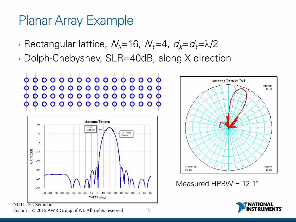
Planar Array Example
• Rectangular lattice, NX=16, NY=4, dX=dY=l/2
• Dolph-Chebyshev, SLR=40dB, along X direction
Measured HPBW = 12.1

ni.com NCTU 5G Seminar
ni.com | © 2015 AWR Group of NI. All rights reserved
Implement Array in EM Tools

ni.com NCTU 5G Seminar
ni.com | © 2015 AWR Group of NI. All rights reserved
Feeding Design and Insitu Antenna 3D Pattern
-90
-90
00
1
2
3
4
QHYB
PHASE2A=-90 Deg
180
0
00
1
2
3
4
DHYB
CAPID=C1C=c pF
CAPID=C2C=c pF
M_PROBEID=VP1
M_PROBEID=VP2
NL_AMPID=AM2GAIN=-6 dBNF=0 dBIP2H=40 dBmIP3=30 dBmP1DB=10 dBm
1
2
SUBCKTID=S1NET="Single Element"
PORT1P=1Z=50 OhmPwr={0} dBm
PORTP=2Z=50 Ohm
c=7
ni.com NCTU 5G Seminar
ni.com | © 2015 AWR Group of NI. All rights reserved
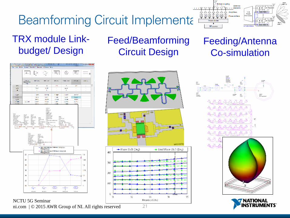
Beamforming Circuit Implementation
-90
-90
00
1
2
3
4
QHYB
PHASE2A=-150 Deg
180
0
00
1
2
3
4
DHYB
CAPID=C1C=c pF
CAPID=C2C=c pF
M_PROBEID=VP1
M_PROBEID=VP2
NL_AMPID=AM2GAIN=-6 dBNF=0 dBIP2H=40 dBmIP3=30 dBmP1DB=10 dBm
1
2
SUBCKTID=S1NET="Single Element"
PORT1P=1Z=50 OhmPwr={0} dBm
PORTP=2Z=50 Ohm
c=7
TRX module Link-
budget/ Design Feed/Beamforming
Circuit Design Feeding/Antenna
Co-simulation

ni.com NCTU 5G Seminar
ni.com | © 2015 AWR Group of NI. All rights reserved
Full RF System Analysis in VSS
TPID=in
TPID=out
PHARRAYID=A1THETA=THETA RadPHI=PHI RadTHETA_ST=rad(THETA_st_deg) RadPHI_ST=
802.11ac
TX
B
1
2
80211ACID=A2TX_Mode=MCS=6: 64QAM, r=3/4TX_Power=-10 dBmBandwidth=Channel BW 80MHzGuardInterval=800nPayload=1024SMPSYM=_SMPSYMCTRFRQ=5.250 GHz
802.11ac
RX
EVM (sc) (sym)
P
IQ
B
1 2
3
4
5 6 7
80211ACID=A4Bandwidth=Auto
TPID=Constellation1
TPID=DUT_In1
TPID=DUT_Out1
TPID=EVM1
TPID=EVM_vs_Subcarrier1
TPID=EVM_vs_Symbol1
TPID=Power1
TPID=Rx_Bitstream1
TPID=TxBitstream1
Fading
MULTIPATH_FADINGID=A5CTRFRQSEL=PropagatedPATHLOSS=40
1
2
3
4
SUBCKTID=S1NET="TGC2610_SM"
THETA = 55
constants("c0") : Frq = CtrFrq*1.01CtrFrq = 5.25e9
N = 4 PHI = 0M = 4
THETA_st_deg=0AMP_B2ID=A3GAIN=10P1DB=10IP3= IP2= MEASREF= OSAT= NF=3NOISE=AutoRFIFRQ=
OSC_SID=A6NET="M"PORT=1FRQ= HARMIDX=1PWR= PHS=0 DegCTRFRQ= SMPFRQ= ZS=_Z0 OhmTN=_TAMB DegKNOISE=AutoPNOISE=No phase noise
2.05 2.1 2.15
Frequency (GHz)
Spectrum_interband_a
-120
-110
-100
-90
-80
-70
-60
-50
-40
-30
-20
-10
0
10
DUT In (dBm)
DUT In2 (dBm)
DB(PWR_SPEC(TP.TP1,1000,0,10,0,-1,0,-1,1,0,4,0,1,0)) (dBm)
d1: Graphs_Auto
d2: Graphs_Auto
d3: Graphs_Auto-45 -25 -5 10
Output Power vs Input Power
-20
-15
-10
-5
0
5p1
DB(Re(P_node(TP.TP1,TP.TP2,0,1,0)))[*,X] (dBm)RF_PID Feedback
p1: Signal Node Power, dBmFreq=1 GHz
ni.com NCTU 5G Seminar
ni.com | © 2015 AWR Group of NI. All rights reserved
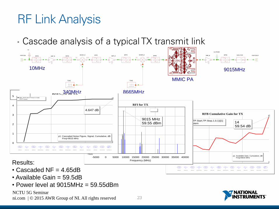
RFB Cumulative Gain for TX
-20
0
20
40
60
S4\BPFB (F1) S4\AMP_B (A1) S4\BPFB (F2) S4\MIXER_B (Mixer1) S4\BPFE (F3) S4\AMP_B (A2) S4\BPFE (F4) S4\MIXER_B (Mixer2) S4\BPFB (F5) S4\AMP_B (A5) S4\AMP_B (A4) S4\BPFB (F6) S4\ISOLATOR (S8) TX_ANTENNA (S7)
p1
1459.54 dB
DB(C_GA(TP.Start,TP.Stop,1,0,1))[1]RFB Tx System
p1: Available Gain, Cumulative, dBFreq=9015 MHz-5000 0 5000 10000 15000 20000 25000 30000 35000 40000
Frequency (MHz)
RFI for TX
-400
-300
-200
-100
0
100
9015 MHz59.55 dBm
RFB C_NF for TX
0
1
2
3
4
5
S4\BPFB (F1) S4\AMP_B (A1) S4\BPFB (F2) S4\MIXER_B (Mixer1) S4\BPFE (F3) S4\AMP_B (A2) S4\BPFE (F4) S4\MIXER_B (Mixer2) S4\BPFB (F5) S4\AMP_B (A5) S4\AMP_B (A4) S4\BPFB (F6) S4\ISOLATOR (S8) TX_ANTENNA (S7)
p1
4.647 dB
DB(C_NF(TP.Start,TP.Stop,0,1,0,1))[1]
RFB Tx System
p1: Cascaded Noise Figure, Signal, Cumulative, dBFreq=9015 MHz
RF Link Analysis
• Cascade analysis of a typical TX transmit link
PORTDOUTPORTDIN AMP_B
1 2
NL_S
ISOLATOR
M_PROBE
BPFB
MMIC PA
340MHz
10MHz
8665MHz
9015MHz
Behavioral PA
or
BPFE BPFBBPFBBPFB AMP_BAMP_B
TP
TONETONE
IN OUT
LO
MIXER_B
IN OUT
LO
MIXER_B BPFE
AMP_B
Results:
• Cascaded NF = 4.65dB
• Available Gain = 59.5dB
• Power level at 9015MHz = 59.55dBm

ni.com NCTU 5G Seminar
ni.com | © 2015 AWR Group of NI. All rights reserved
Time EVM Power (ns) System Diagram 1 System Diagram 1 1.6e+005 -36.65 -0.032489 1.64e+005 -36.649 -0.032488 1.68e+005 -36.65 -0.03249 1.72e+005 -36.65 -0.032486 1.76e+005 -36.647 -0.032486 1.8e+005 -36.649 -0.032489 1.84e+005 -36.649 -0.032486 1.88e+005 -36.65 -0.032488 1.92e+005 -36.65 -0.03249
System Level Design and Analysis
• Signal sources and receivers from LabVIEW
• Conformance test benches • Standard and custom measurements
• Seamless integration with circuit designs (MWO)
• Blazing fast simulations!
ni.com NCTU 5G Seminar
ni.com | © 2015 AWR Group of NI. All rights reserved
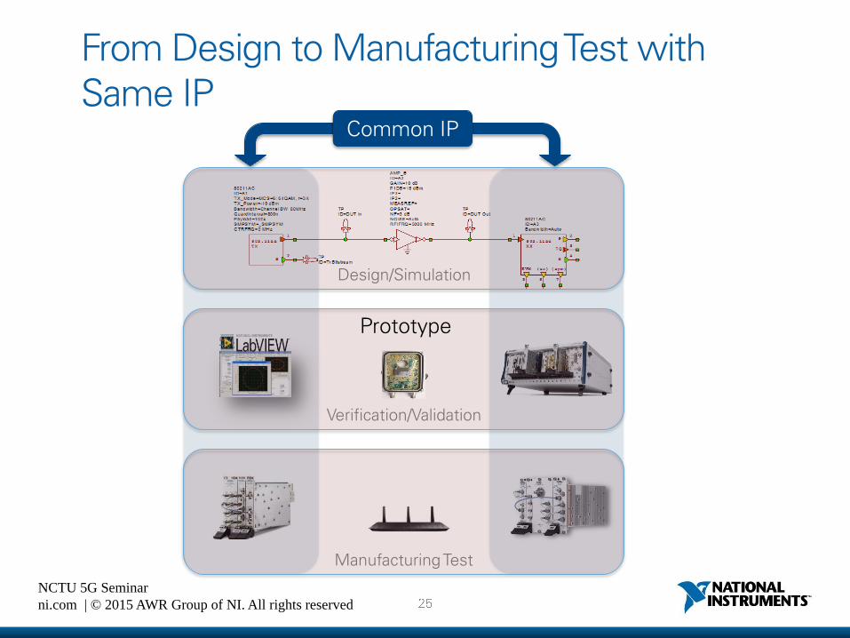
From Design to Manufacturing Test with Same IP
Verification/Validation
Manufacturing Test
Common IP
Design/Simulation
Prototype
ni.com NCTU 5G Seminar
ni.com | © 2015 AWR Group of NI. All rights reserved
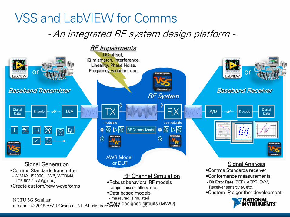
VSS and LabVIEW for Comms
Signal Analysis •Comms Standards receiver •Conformance measurements - Bit Error Rate (BER), ACPR, EVM, Receiver sensitivity, etc.
•Custom IP, algorithm development
Baseband Transmitter
RF Impairments
Baseband Receiver
RF Channel Simulation •Robust behavioral RF models - amps, mixers, filters, etc.,
•Data based models - measured, simulated
•AWR designed circuits (MWO)
RF System
- An integrated RF system design platform -
TX RX
RF Channel Model
DC offset, IQ mismatch, Interference,
Linearity, Phase Noise, Frequency variation, etc.,
Signal Generation •Comms Standards transmitter - WiMAX, IS2000, UWB, WCDMA, LTE,802.11a/b/g, etc.,
•Create custom/new waveforms
C R
Digital Data
Encode D/A Decode Digital Data A/D
-0.4 -0.2 0 0.2 0.4
IQ
-0.4
-0.2
0
0.2
0.4
IQ(TP.Spectrum,300,1,1,0,0,0)
System
-105 -95 -85 -75 -65 -55 -45 -35 -25
SNR
5
10
15
20
25
30
DB(ACPR(VSA.M1,10.1,4,0.1,-1,-0.1,4,0.1,4,1,0,1,0,0,0,0.5,0.01,5,10,2))[x]
Increasing Sweep
DB(ACPR(VSA.M1,10.1,4,0.1,-1,-0.1,4,0.1,4,1,0,1,0,0,0,0.5,0.01,5,10,2))[x]
Decreasing Sweep
DB(ACPR(VSA.M1,10.1,4,0.1,-1,-0.1,4,0.1,4,1,0,1,0,0,0,0.5,0.01,5,10,2))[x]
Increasing Sweep No Hyst
DB(ACPR(VSA.M1,10.1,4,0.1,-1,-0.1,4,0.1,4,1,0,1,0,0,0,0.5,0.01,5,10,2))[x]
Decreasing Sweep No Hyst
AWR Model or DUT
or or
modulate de-modulate