ARM – Memory Management Unit · – Two 16-KByte Internal SRAM, Single-cycle Access at Maximum...
42
NOTE: This is a summary document. The complete document is available on the Atmel website at www.atmel.com. Features • Incorporates the ARM926EJ-S ™ ARM ® Thumb ® Processor – DSP Instruction Extensions, ARM Jazelle ® Technology for Java ® Acceleration – 32-KByte Data Cache, 32-KByte Instruction Cache, Write Buffer – CPU Frequency 400 MHz – Memory Management Unit – EmbeddedICE ™ , Debug Communication Channel Support • Additional Embedded Memories – One 64-KByte Internal ROM, Single-cycle Access at Maximum Matrix Speed – Two 16-KByte Internal SRAM, Single-cycle Access at Maximum Matrix Speed • External Bus Interface (EBI) – Supports SDRAM, Static Memory, ECC-enabled NAND Flash and CompactFlash ® • USB 2.0 Full Speed (12 Mbits per second) Device Port – On-chip Transceiver, 2,432-byte Configurable Integrated DPRAM • USB 2.0 Full Speed (12 Mbits per second) Host and Double Port – Single or Dual On-chip Transceivers – Integrated FIFOs and Dedicated DMA Channels • Ethernet MAC 10/100 Base T – Media Independent Interface or Reduced Media Independent Interface – 128-byte FIFOs and Dedicated DMA Channels for Receive and Transmit • Image Sensor Interface – ITU-R BT. 601/656 External Interface, Programmable Frame Capture Rate – 12-bit Data Interface for Support of High Sensibility Sensors – SAV and EAV Synchronization, Preview Path with Scaler, YCbCr Format • Bus Matrix – Six 32-bit-layer Matrix – Boot Mode Select Option, Remap Command • Fully-featured System Controller, including – Reset Controller, Shutdown Controller – Four 32-bit Battery Backup Registers for a Total of 16 Bytes – Clock Generator and Power Management Controller – Advanced Interrupt Controller and Debug Unit – Periodic Interval Timer, Watchdog Timer and Real-time Timer • Reset Controller (RSTC) – Based on a Power-on Reset Cell, Reset Source Identification and Reset Output Control • Clock Generator (CKGR) – Selectable 32,768 Hz Low-power Oscillator or Internal Low Power RC Oscillator on Battery Backup Power Supply, Providing a Permanent Slow Clock – 3 to 20 MHz On-chip Oscillator, One up to 800 MHz PLL and One up to 100 MHz PLL • Power Management Controller (PMC) – Very Slow Clock Operating Mode, Software Programmable Power Optimization Capabilities – Two Programmable External Clock Signals • Advanced Interrupt Controller (AIC) – Individually Maskable, Eight-level Priority, Vectored Interrupt Sources – Three External Interrupt Sources and One Fast Interrupt Source, Spurious Interrupt Protected • Debug Unit (DBGU) – 2-wire UART and Support for Debug Communication Channel, Programmable ICE Access Prevention – Mode for General Purpose 2-wire UART Serial Communication AT91 ARM Thumb Microcontrollers AT91SAM9G20 Summary 6384DS–ATARM–13-Jan-10
Transcript of ARM – Memory Management Unit · – Two 16-KByte Internal SRAM, Single-cycle Access at Maximum...

NOTE: This is a summary document. The complete document is available on the Atmel website at www.atmel.com.
AT91 ARM Thumb Microcontrollers
AT91SAM9G20 Summary
6384DS–ATARM–13-Jan-10
Features• Incorporates the ARM926EJ-S™ ARM® Thumb® Processor
– DSP Instruction Extensions, ARM Jazelle® Technology for Java® Acceleration– 32-KByte Data Cache, 32-KByte Instruction Cache, Write Buffer– CPU Frequency 400 MHz– Memory Management Unit– EmbeddedICE™, Debug Communication Channel Support
• Additional Embedded Memories– One 64-KByte Internal ROM, Single-cycle Access at Maximum Matrix Speed– Two 16-KByte Internal SRAM, Single-cycle Access at Maximum Matrix Speed
• External Bus Interface (EBI)– Supports SDRAM, Static Memory, ECC-enabled NAND Flash and CompactFlash®
• USB 2.0 Full Speed (12 Mbits per second) Device Port– On-chip Transceiver, 2,432-byte Configurable Integrated DPRAM
• USB 2.0 Full Speed (12 Mbits per second) Host and Double Port– Single or Dual On-chip Transceivers– Integrated FIFOs and Dedicated DMA Channels
• Ethernet MAC 10/100 Base T– Media Independent Interface or Reduced Media Independent Interface – 128-byte FIFOs and Dedicated DMA Channels for Receive and Transmit
• Image Sensor Interface– ITU-R BT. 601/656 External Interface, Programmable Frame Capture Rate– 12-bit Data Interface for Support of High Sensibility Sensors– SAV and EAV Synchronization, Preview Path with Scaler, YCbCr Format
• Bus Matrix– Six 32-bit-layer Matrix– Boot Mode Select Option, Remap Command
• Fully-featured System Controller, including– Reset Controller, Shutdown Controller– Four 32-bit Battery Backup Registers for a Total of 16 Bytes– Clock Generator and Power Management Controller– Advanced Interrupt Controller and Debug Unit– Periodic Interval Timer, Watchdog Timer and Real-time Timer
• Reset Controller (RSTC)– Based on a Power-on Reset Cell, Reset Source Identification and Reset Output
Control• Clock Generator (CKGR)
– Selectable 32,768 Hz Low-power Oscillator or Internal Low Power RC Oscillator on Battery Backup Power Supply, Providing a Permanent Slow Clock
– 3 to 20 MHz On-chip Oscillator, One up to 800 MHz PLL and One up to 100 MHz PLL• Power Management Controller (PMC)
– Very Slow Clock Operating Mode, Software Programmable Power Optimization Capabilities
– Two Programmable External Clock Signals• Advanced Interrupt Controller (AIC)
– Individually Maskable, Eight-level Priority, Vectored Interrupt Sources– Three External Interrupt Sources and One Fast Interrupt Source, Spurious
Interrupt Protected• Debug Unit (DBGU)
– 2-wire UART and Support for Debug Communication Channel, Programmable ICE Access Prevention
– Mode for General Purpose 2-wire UART Serial Communication

• Periodic Interval Timer (PIT)– 20-bit Interval Timer plus 12-bit Interval Counter
• Watchdog Timer (WDT)– Key-protected, Programmable Only Once, Windowed 16-bit Counter Running at Slow Clock
• Real-time Timer (RTT)– 32-bit Free-running Backup Counter Running at Slow Clock with 16-bit Prescaler
• One 4-channel 10-bit Analog-to-Digital Converter• Three 32-bit Parallel Input/Output Controllers (PIOA, PIOB, PIOC)
– 96 Programmable I/O Lines Multiplexed with up to Two Peripheral I/Os – Input Change Interrupt Capability on Each I/O Line– Individually Programmable Open-drain, Pull-up Resistor and Synchronous Output– All I/O Lines are Schmitt Trigger Inputs
• Peripheral DMA Controller Channels (PDC)• One Two-slot MultiMedia Card Interface (MCI)
– SDCard/SDIO and MultiMediaCard™ Compliant – Automatic Protocol Control and Fast Automatic Data Transfers with PDC
• One Synchronous Serial Controller (SSC)– Independent Clock and Frame Sync Signals for Each Receiver and Transmitter– I²S Analog Interface Support, Time Division Multiplex Support– High-speed Continuous Data Stream Capabilities with 32-bit Data Transfer
• Four Universal Synchronous/Asynchronous Receiver Transmitters (USART)– Individual Baud Rate Generator, IrDA® Infrared Modulation/Demodulation, Manchester Encoding/Decoding– Support for ISO7816 T0/T1 Smart Card, Hardware Handshaking, RS485 Support– Full Modem Signal Control on USART0
• Two 2-wire UARTs• Two Master/Slave Serial Peripheral Interfaces (SPI)
– 8- to 16-bit Programmable Data Length, Four External Peripheral Chip Selects– Synchronous Communications
• Two Three-channel 16-bit Timer/Counters (TC)– Three External Clock Inputs, Two Multi-purpose I/O Pins per Channel– Double PWM Generation, Capture/Waveform Mode, Up/Down Capability– High-Drive Capability on Outputs TIOA0, TIOA1, TIOA2
• One Two-wire Interface (TWI)– Compatible with Standard Two-wire Serial Memories– One, Two or Three Bytes for Slave Address– Sequential Read/Write Operations– Master, Multi-master and Slave Mode Operation– Bit Rate: Up to 400 Kbits– General Call Supported in Slave Mode– Connection to Peripheral DMA Controller (PDC) Channel Capabilities Optimizes Data Transfers in Master Mode
• IEEE® 1149.1 JTAG Boundary Scan on All Digital Pins• Required Power Supplies
– 0.9V to 1.1V for VDDBU, VDDCORE, VDDPLL– 1.65 to 3.6V for VDDOSC – 1.65V to 3.6V for VDDIOP (Peripheral I/Os) – 3.0V to 3.6V for VDDUSB– 3.0V to 3.6V VDDANA (Analog-to-digital Converter)– Programmable 1.65V to 1.95V or 3.0V to 3.6V for VDDIOM (Memory I/Os)
• Available in a 217-ball LFBGA and 247-ball TFBGA RoHS-compliant Package
26384DS–ATARM–13-Jan-10
AT91SAM9G20 Summary

AT91SAM9G20 Summary
1. DescriptionThe AT91SAM9G20 is based on the integration of an ARM926EJ-S processor with fast ROMand RAM memories and a wide range of peripherals.
The AT91SAM9G20 embeds an Ethernet MAC, one USB Device Port, and a USB Host control-ler. It also integrates several standard peripherals, such as the USART, SPI, TWI, TimerCounters, Synchronous Serial Controller, ADC and MultiMedia Card Interface.
The AT91SAM9G20 is architectured on a 6-layer matrix, allowing a maximum internal bandwidthof six 32-bit buses. It also features an External Bus Interface capable of interfacing with a widerange of memory devices.
The AT91SAM9G20 is an enhancement of the AT91SAM9260 with the same peripheral fea-tures. It is pin-to-pin compatible with the exception of power supply pins. Speed is increased toreach 400 MHz on the ARM core and 133 MHz on the system bus and EBI.
36384DS–ATARM–13-Jan-10
2. AT91SAM9G20 Block Diagram
Figure 2-1. AT91SAM9G20 Block Diagram
AR
M92
6EJ-
S P
roce
ssor
JTA
G S
elec
tion
and
Bou
ndar
y S
can
In-C
ircui
t Em
ulat
orA
IC
Fast
SR
AM
16
Kby
tes
D0-
D15
A0/
NB
S0
A2-
A15
, A18
-A20
A16
/BA
0A
17/B
A1
NC
S0
NC
S1/
SD
CS
NR
D/C
FO
EN
WR
0/N
WE
/CF
WE
NW
R1/
NB
S1/
CF
IOR
NW
R3/
NB
S3/
CF
IOW
SD
CK
, SD
CK
ER
AS
, CA
SS
DW
E, S
DA
10
FIQ
IRQ
0-IR
Q2
DR
XD
DT
XD
MM
U
AP
B
RO
M64
Kby
tes
Per
iphe
ral
Brid
ge24
-cha
nnel
Per
iphe
ral
DM
A
Bus
Inte
rfac
e
A1/
NB
S2/
NW
R2
TS
T
PC
K0-
PC
K1
Sys
tem
C
ontr
olle
r
XIN
TDI TDO TMS TCK
JTAGSEL
ID
NA
ND
OE
, NA
ND
WE
PM
C
OS
CX
OU
T
PIT
WD
T
DB
GU
SLA
VE
MA
ST
ER
PD
C
BMS
A23
-A24
NC
S5/
CF
CS
1A
25/C
FR
NW
NC
S4/
CF
CS
0
NW
AIT
CF
CE
1-C
FC
E2
EB
I
Sta
ticM
emor
yC
ontr
olle
r
Com
pact
Fla
shN
AN
D F
lash
SD
RA
MC
ontr
olle
r
NC
S2,
NC
S6,
NC
S7
NC
S3/
NA
ND
CS
RTCK
EC
CC
ontr
olle
r
ETXCK-ERXCK
ETXEN-ETXER
ECRS-ECOL
ERXER-ERXDV
ERX0-ERX3
ETX0-ETX3
MDC MDIO F100
10/1
00 E
ther
net
MA
C
FIF
O
DM
A
FIF
O
SS
C
PD
C
US
B
Dev
ice
DDM DDP
TKTFTDRDRFRK
TC
0T
C1
TC
2
TCLK0-
TCLK2
TIOA0-
TIOA2
TIOB0-
TIOB2
SP
I0S
PI1
PD
C
US
AR
T0
US
AR
T1
US
AR
T2
US
AR
T3
US
AR
T4
US
AR
T5
RTS0-RTS3
SCK0-SCK2
TXD0-TXD5
RXD0-RXD5
CTS0-CTS3
PD
C
TW
I
TWCK
TWD
MC
I
PD
C
Tran
scei
ver
DP
RA
M
ICac
he32
K b
ytes
DC
ache
32K
byt
es
6-la
yer
Mat
rix6
x 10
0M x
32-
bit w
ords
NPCS2NPCS1SPCK MOSI MIS
O
NPCS0
NPCS3
SP
I0_,
SP
I1_
MCCK
MCDA0-MCDA3MCCDA
NR
ST
XIN
32X
OU
T32
VD
DC
OR
E
PIO
A
PIO
B
PIO
C
DSR0 DCD0DTR0
RI0
US
B
OH
CI
DM
ATran
sc.
Tran
sc.
HDPA HDMAHDPB HDMB
Imag
e S
enso
r In
terf
ace
DM
A
ISI_P
CKIS
I_DO-IS
I_D7
ISI_H
SYNC
ISI_V
SYNC
ISI_M
CK
4-ch
anne
l10
-bit
AD
CAD0-
AD3 ADTRIGADVREF VDDANA GNDANA
PD
C
D16
-D31
RT
TO
SC
RS
TC
PO
R
4GP
RE
G
SH
DN
WK
UP
SH
DC
PO
R
RC
OS
CS
EL
VD
DB
U
MCDB0-MCDB3 MCCDB
TC
3T
C4
TC
5
TCLK3-
TCLK5
TIOA3-
TIOA5
TIOB3-
TIOB5
Fast
SR
AM
16
Kby
tes
PD
C
A21
/NA
ND
ALE
, A22
/NA
ND
CLE
PLL
A
Filter Filter
PLL
B
46384DS–ATARM–13-Jan-10
AT91SAM9G20 Summary

AT91SAM9G20 Summary
3. Signal Description
Table 3-1. Signal Description List (Continued)
Signal Name Function TypeActive Level Comments
Power Supplies
VDDIOM EBI I/O Lines Power Supply Power 1.65V to 1.95V or 3.0V to 3.6V
VDDIOP Peripherals I/O Lines Power Supply Power 1.65V to 3.6V
VDDBU Backup I/O Lines Power Supply Power 0.9V to 1.1V
VDDANA Analog Power Supply Power 3.0V to 3.6V
VDDPLL PLL Power Supply Power 0.9V to 1.1V
VDDOSC Oscillator Power Supply Power 1.65V to 3.6V
VDDCORE Core Chip Power Supply Power 0.9V to 1.1V
VDDUSB USB Power Supply Power 1.65V to 3.6V
GND Ground Ground
GNDANA Analog Ground Ground
GNDBU Backup Ground Ground
GNDUSB USB Ground Ground
GNDPLL PLL Ground Ground
Clocks, Oscillators and PLLs
XIN Main Oscillator Input Input
XOUT Main Oscillator Output Output
XIN32 Slow Clock Oscillator Input Input
XOUT32 Slow Clock Oscillator Output Output
OSCSEL Slow Clock Oscillator Selection InputAccepts between 0V and VDDBU.
PCK0 - PCK1 Programmable Clock Output Output
Shutdown, Wakeup Logic
SHDN Shutdown Control Output
WKUP Wake-up Input InputAccepts between 0V and VDDBU.
ICE and JTAG
NTRST Test Reset Signal Input Low Pull-up resistor
TCK Test Clock Input No pull-up resistor
TDI Test Data In Input No pull-up resistor
TDO Test Data Out Output
TMS Test Mode Select Input No pull-up resistor
JTAGSEL JTAG Selection InputPull-down resistor. Accepts between 0V and VDDBU.
RTCK Return Test Clock Output
56384DS–ATARM–13-Jan-10

Reset/Test
NRST Microcontroller Reset I/O Low Pull-up resistor
TST Test Mode Select InputPull-down resistor. Accepts between 0V and VDDBU.
BMS Boot Mode Select InputNo pull-up resistorBMS = 0 when tied to GND.
BMS = 1 when tied to VDDIOP.
Debug Unit - DBGU
DRXD Debug Receive Data Input
DTXD Debug Transmit Data Output
Advanced Interrupt Controller - AIC
IRQ0 - IRQ2 External Interrupt Inputs Input
FIQ Fast Interrupt Input Input
PIO Controller - PIOA - PIOB - PIOC
PA0 - PA31 Parallel IO Controller A I/O Pulled-up input at reset
PB0 - PB31 Parallel IO Controller B I/O Pulled-up input at reset
PC0 - PC31 Parallel IO Controller C I/O Pulled-up input at reset
External Bus Interface - EBI
D0 - D31 Data Bus I/O Pulled-up input at reset
A0 - A25 Address Bus Output 0 at reset
NWAIT External Wait Signal Input Low
Static Memory Controller - SMC
NCS0 - NCS7 Chip Select Lines Output Low
NWR0 - NWR3 Write Signal Output Low
NRD Read Signal Output Low
NWE Write Enable Output Low
NBS0 - NBS3 Byte Mask Signal Output Low
CompactFlash Support
CFCE1 - CFCE2 CompactFlash Chip Enable Output Low
CFOE CompactFlash Output Enable Output Low
CFWE CompactFlash Write Enable Output Low
CFIOR CompactFlash IO Read Output Low
CFIOW CompactFlash IO Write Output Low
CFRNW CompactFlash Read Not Write Output
CFCS0 - CFCS1 CompactFlash Chip Select Lines Output Low
Table 3-1. Signal Description List (Continued)
Signal Name Function TypeActive Level Comments
66384DS–ATARM–13-Jan-10
AT91SAM9G20 Summary
AT91SAM9G20 Summary
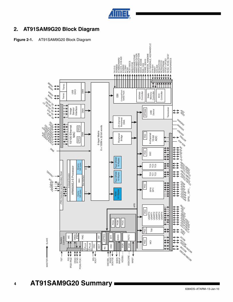
NAND Flash Support
NANDCS NAND Flash Chip Select Output Low
NANDOE NAND Flash Output Enable Output Low
NANDWE NAND Flash Write Enable Output Low
NANDALE NAND Flash Address Latch Enable Output Low
NANDCLE NAND Flash Command Latch Enable Output Low
SDRAM Controller
SDCK SDRAM Clock Output
SDCKE SDRAM Clock Enable Output High
SDCS SDRAM Controller Chip Select Output Low
BA0 - BA1 Bank Select Output
SDWE SDRAM Write Enable Output Low
RAS - CAS Row and Column Signal Output Low
SDA10 SDRAM Address 10 Line Output
Multimedia Card Interface MCI
MCCK Multimedia Card Clock Output
MCCDA Multimedia Card Slot A Command I/O
MCDA0 - MCDA3 Multimedia Card Slot A Data I/O
MCCDB Multimedia Card Slot B Command I/O
MCDB0 - MCDB3 Multimedia Card Slot B Data I/O
Universal Synchronous Asynchronous Receiver Transmitter USARTx
SCKx USARTx Serial Clock I/O
TXDx USARTx Transmit Data I/O
RXDx USARTx Receive Data Input
RTSx USARTx Request To Send Output
CTSx USARTx Clear To Send Input
DTR0 USART0 Data Terminal Ready Output
DSR0 USART0 Data Set Ready Input
DCD0 USART0 Data Carrier Detect Input
RI0 USART0 Ring Indicator Input
Synchronous Serial Controller - SSC
TD SSC Transmit Data Output
RD SSC Receive Data Input
TK SSC Transmit Clock I/O
RK SSC Receive Clock I/O
TF SSC Transmit Frame Sync I/O
RF SSC Receive Frame Sync I/O
Table 3-1. Signal Description List (Continued)
Signal Name Function TypeActive Level Comments
76384DS–ATARM–13-Jan-10

Timer/Counter - TCx
TCLKx TC Channel x External Clock Input Input
TIOAx TC Channel x I/O Line A I/O
TIOBx TC Channel x I/O Line B I/O
Serial Peripheral Interface - SPIx_
SPIx_MISO Master In Slave Out I/O
SPIx_MOSI Master Out Slave In I/O
SPIx_SPCK SPI Serial Clock I/O
SPIx_NPCS0 SPI Peripheral Chip Select 0 I/O Low
SPIx_NPCS1-SPIx_NPCS3 SPI Peripheral Chip Select Output Low
Two-Wire Interface
TWD Two-wire Serial Data I/O
TWCK Two-wire Serial Clock I/O
USB Host Port
HDPA USB Host Port A Data + Analog
HDMA USB Host Port A Data - Analog
HDPB USB Host Port B Data + Analog
HDMB USB Host Port B Data - Analog
USB Device Port
DDM USB Device Port Data - Analog
DDP USB Device Port Data + Analog
Ethernet 10/100
ETXCK Transmit Clock or Reference Clock Input MII only, REFCK in RMII
ERXCK Receive Clock Input MII only
ETXEN Transmit Enable Output
ETX0-ETX3 Transmit Data Output ETX0-ETX1 only in RMII
ETXER Transmit Coding Error Output MII only
ERXDV Receive Data Valid Input RXDV in MII, CRSDV in RMII
ERX0-ERX3 Receive Data Input ERX0-ERX1 only in RMII
ERXER Receive Error Input
ECRS Carrier Sense and Data Valid Input MII only
ECOL Collision Detect Input MII only
EMDC Management Data Clock Output
EMDIO Management Data Input/Output I/O
Table 3-1. Signal Description List (Continued)
Signal Name Function TypeActive Level Comments
86384DS–ATARM–13-Jan-10
AT91SAM9G20 Summary

AT91SAM9G20 Summary
Note: No PLLRCA line present on the AT91SAM9G20.
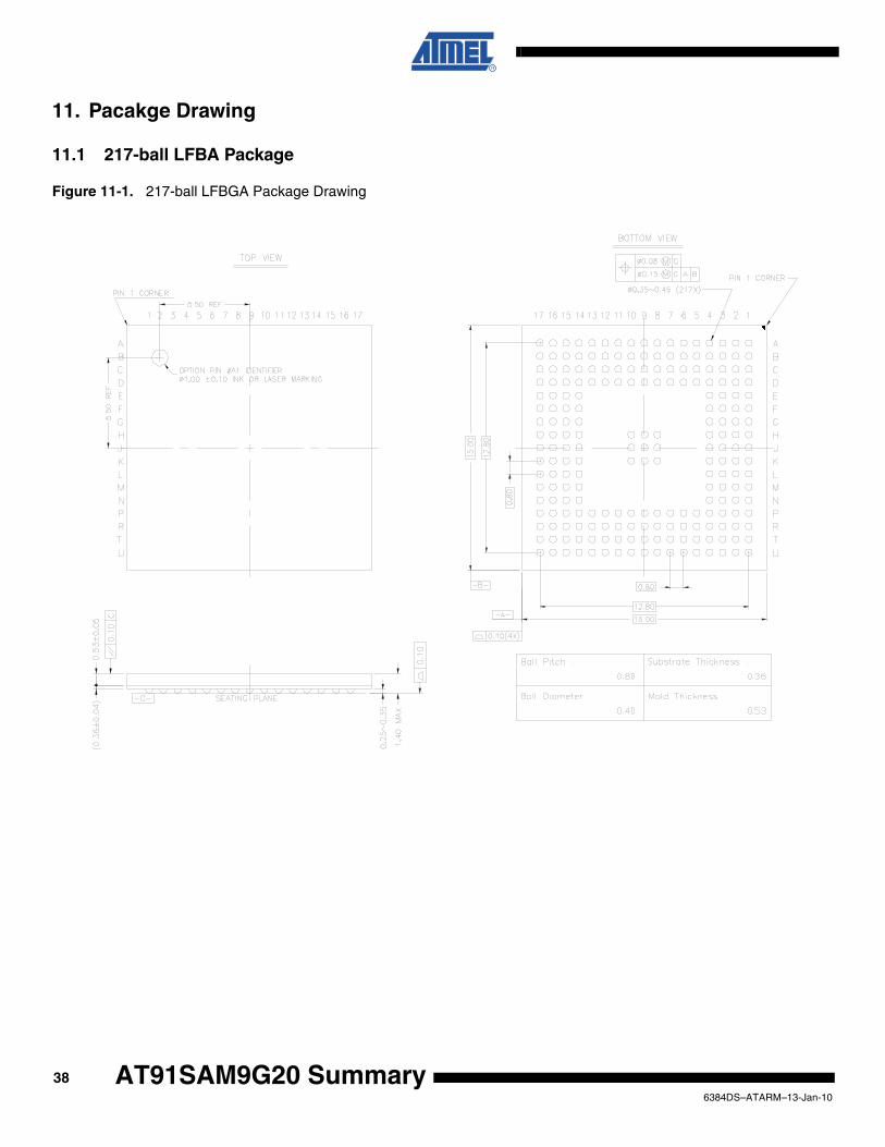
4. Package and Pinout• The AT91SAM9G20 is available in a 217-ball, 15 x 15 mm, LFBGA package (0.8 mm pitch)
(Figure 4-1).
• The AT91SAM9G20 is available in a 247-ball, 10 x 10 x 1.1 mm, TFBGA Green package, , (0.5 mm pitch) (Figure 4-2).
4.1 217-ball LFBGA Package OutlineFigure 4-1 shows the orientation of the 217-ball LFBGA package.
A detailed mechanical description is given in the section “AT91SAM9G20 Mechanical Charac-teristics” of the product datasheet.
Figure 4-1. 217-ball LFBGA Package (Top View)
Image Sensor Interface
ISI_D0-ISI_D11 Image Sensor Data Input
ISI_MCK Image Sensor Reference Clock Output
ISI_HSYNC Image Sensor Horizontal Synchro Input
ISI_VSYNC Image Sensor Vertical Synchro Input
ISI_PCK Image Sensor Data clock Input
Analog to Digital Converter
AD0-AD3 Analog Inputs Analog Digital pulled-up inputs at reset
ADVREF Analog Positive Reference Analog
ADTRG ADC Trigger Input
Table 3-1. Signal Description List (Continued)
Signal Name Function TypeActive Level Comments
12
1234567891011
1314151617
A B C D E F G H J K L M N P R T UBall A1
96384DS–ATARM–13-Jan-10

4.2 217-ball LFBGA Pinout
Table 4-1. Pinout for 217-ball LFBGA PackagePin Signal Name Pin Signal Name Pin Signal Name Pin Signal NameA1 CFIOW/NBS3/NWR3 D5 A5 J14 TDO P17 PB5A2 NBS0/A0 D6 GND J15 PB19 R1 NCA3 NWR2/NBS2/A1 D7 A10 J16 TDI R2 GNDANAA4 A6 D8 GND J17 PB16 R3 PC29A5 A8 D9 VDDCORE K1 PC24 R4 VDDANAA6 A11 D10 GNDUSB K2 PC20 R5 PB12A7 A13 D11 VDDIOM K3 D15 R6 PB23A8 BA0/A16 D12 GNDUSB K4 PC21 R7 GNDA9 A18 D13 DDM K8 GND R8 PB26A10 A21 D14 HDPB K9 GND R9 PB28A11 A22 D15 NC K10 GND R10 PA0A12 CFWE/NWE/NWR0 D16 VDDBU K14 PB4 R11 PA4A13 CFOE/NRD D17 XIN32 K15 PB17 R12 PA5A14 NCS0 E1 D10 K16 GND R13 PA10A15 PC5 E2 D5 K17 PB15 R14 PA21A16 PC6 E3 D3 L1 GND R15 PA23A17 PC4 E4 D4 L2 PC26 R16 PA24B1 SDCK E14 HDPA L3 PC25 R17 PA29B2 CFIOR/NBS1/NWR1 E15 HDMA L4 VDDOSC T1 NCB3 SDCS/NCS1 E16 GNDBU L14 PA28 T2 GNDPLLB4 SDA10 E17 XOUT32 L15 PB9 T3 PC0B5 A3 F1 D13 L16 PB8 T4 PC1B6 A7 F2 SDWE L17 PB14 T5 PB10B7 A12 F3 D6 M1 VDDCORE T6 PB22B8 A15 F4 GND M2 PC31 T7 GNDB9 A20 F14 OSCSEL M3 GND T8 PB29B10 NANDWE F15 BMS M4 PC22 T9 PA2B11 PC7 F16 JTAGSEL M14 PB1 T10 PA6B12 PC10 F17 TST M15 PB2 T11 PA8B13 PC13 G1 PC15 M16 PB3 T12 PA11B14 PC11 G2 D7 M17 PB7 T13 VDDCOREB15 PC14 G3 SDCKE N1 XIN T14 PA20B16 PC8 G4 VDDIOM N2 VDDPLL T15 GNDB17 WKUP G14 GND N3 PC23 T16 PA22C1 D8 G15 NRST N4 PC27 T17 PA27C2 D1 G16 RTCK N14 PA31 U1 GNDPLLC3 CAS G17 TMS N15 PA30 U2 ADVREFC4 A2 H1 PC18 N16 PB0 U3 PC2C5 A4 H2 D14 N17 PB6 U4 PC3C6 A9 H3 D12 P1 XOUT U5 PB20C7 A14 H4 D11 P2 VDDPLL U6 PB21C8 BA1/A17 H8 GND P3 PC30 U7 PB25C9 A19 H9 GND P4 PC28 U8 PB27C10 NANDOE H10 GND P5 PB11 U9 PA12C11 PC9 H14 VDDCORE P6 PB13 U10 PA13C12 PC12 H15 TCK P7 PB24 U11 PA14C13 DDP H16 NTRST P8 VDDIOP U12 PA15C14 HDMB H17 PB18 P9 PB30 U13 PA19C15 NC J1 PC19 P10 PB31 U14 PA17C16 VDDUSB J2 PC17 P11 PA1 U15 PA16C17 SHDN J3 VDDIOM P12 PA3 U16 PA18D1 D9 J4 PC16 P13 PA7 U17 VDDIOPD2 D2 J8 GND P14 PA9D3 RAS J9 GND P15 PA26D4 D0 J10 GND P16 PA25
106384DS–ATARM–13-Jan-10
AT91SAM9G20 Summary
AT91SAM9G20 Summary
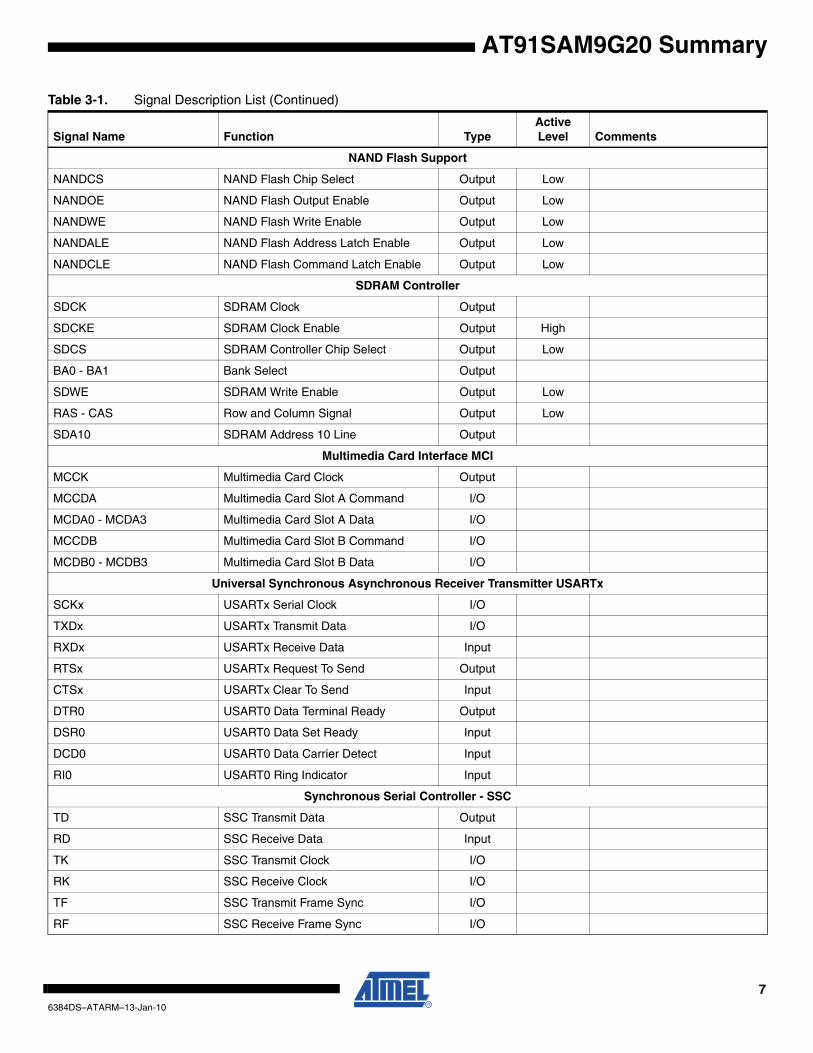
4.3 247-ball TFBGA Package OutlineFigure 4-2 shows the orientation of the 247-ball TFBGA package.
A detailed mechanical description is given in the section “AT91SAM9G20 Mechanical Charac-teristics” of the product datasheet.
Figure 4-2. 247-ball TFBGA Package (Bottom View)
A
B
C
D
E
F
G
H
J
K
L
M
N
P
R
T
U
V
W
1 2 3 4 5 6 7 8 9 10 11 12 13 14 15 16 17 18 19
Ball A1
116384DS–ATARM–13-Jan-10

4.4 247-ball TFBGA Package Pinout
Table 4-2. Pinout for 247-ball TFBGA Package Pin Signal Name Pin Signal Name Pin Signal Name Pin Signal NameA1 D13 F7 CFIOR/NBS1/NWR1 K10 GND P17 RTCK
A2 D12 F8 SDA10 K11 VDDIOM P18 PB16
A12 A9 F9 NBS0/A0 K12 GND R2 GND
A14 A13 F10 A6 K13 GND R3 PB29
A16 A20 F11 A12 K14 XOUT32 R5 PB26
A18 A22 F12 A15 K15 XIN32 R6 PB27
A19 NANDOE F13 BA1/A17 K17 HDPA R7 PA5
B1 D15 F14 PC10 K18 HDMA R8 GND
B2 D14 F15 PC14 L2 NC R9 PA12
B3 D10 F16 VDDUSB L3 NC R10 GND
B4 D9 F17 PC9 L5 ADVREF R11 PA19
B5 D7 F18 PC12 L6 PC2 R12 PA26
B6 D3 G2 PC26 L7 GND R13 PB1
B7 D2 G3 PC25 L8 GND R14 GND
B8 RAS G5 PC24 L9 GND R15 PB7
B9 CAS G6 PC21 L10 GND R17 PB14
B10 NWR2/NBS2/A1 G8 VDDCORE L11 VDDCORE R18 PB9
B11 A3 G9 A5 L12 GND T2 PA1
B13 A10 G10 VDDCORE L13 OSCSEL T3 PB10
B15 A18 G11 VDDCORE L14 GNDBU T17 PB19
B17 A21 G12 VDDCORE L15 GND T18 PB17
B19 VDDUSB G14 PC13 L17 NRST U2 GNDANA
C2 PC15 G15 GND L18 TCK U3 PB21
C3 D11 G17 GNDUSB M2 PC0 U4 PB28
C4 D8 G18 PC11 M3 PC1 U5 PB31
C5 SDCKE H2 PC31 M5 PC3 U6 PA4
C6 SDWE H3 PC30 M6 NTRST U7 PA3
C7 SDCK H5 PC28 M7 GND U8 PA9
C8 D1 H6 PC27 M8 GND U9 GND
C9 SDCS/NCS1 H7 PC29 M9 GND U10 PA15
C10 A2 H8 GND M10 PA16 U11 PA21
C11 A7 H9 GND M11 VDDCORE U12 PA25
C12 A11 H10 VDDIOM M12 GND U13 PA29
C14 A19 H11 VDDIOM M13 VDDIOP U14 PA27
C16 GNDUSB H12 GND M14 TST U15 PA31
C18 CFWE/NWE/NWR0 H13 VDDCORE M15 JTAGSEL U16 GND
D2 PC17 H14 SHDW M17 PB18 U17 PB2
D3 PC16 H15 VDDBU M18 TMS U18 GND
D13 A14 H17 HDPB N2 PB20 V1 PB12
D15 NANDWE H18 HDMB N3 PB13 V2 PB23
D17 CFOE/NRD J2 VDDOSC N5 PB11 V3 PB30
D19 NCS0 J3 VDDPLL N6 BMS V4 PA2
E2 PC18 J5 XOUT N8 GND V5 PA8
E3 PC19 J6 XIN N11 PA17 V6 PA10
E5 D6 J7 VDDPLL N12 PA23 V7 PA13
E6 D5 J8 GND N14 GND V8 VDDIOP
E7 D0 J9 VDDIOM N15 VDDIOP V9 PA14
E8 CFIOW/NBS3/NWR3 J10 VDDIOM N17 TDO V10 VDDIOP
E9 GND J11 VDDIOM N18 TDI V11 PA20
E10 A4 J12 GND P2 PB24 V12 PA22
E11 A8 J13 GND P3 PB22 V13 VDDIOP
E12 VDDIOM J14 WKUP P5 GND V14 PA30
E13 BA0/A16 J15 DDP P6 GND V15 PB0
E14 PC8 J17 DDM P7 PA6 V16 GND
E15 PC4 J18 VDDIOP P8 PA7 V17 PB4
E16 PC5 K2 GNDPLL P9 PA11 V18 GND
E18 PC7 K3 GND P10 GND V19 PB6
E19 PC6 K5 NC P11 PA18 W1 PB25
F2 PC22 K6 GNDPLL P12 PA24 W2 PA0
F3 PC23 K7 VDDANA P13 PA28 W18 PB8
F5 PC20 K8 GND P14 PB3 W19 PB15
F6 D4 K9 GND P15 PB5
126384DS–ATARM–13-Jan-10
AT91SAM9G20 Summary

AT91SAM9G20 Summary
5. Power Considerations
5.1 Power SuppliesThe AT91SAM9G20 has several types of power supply pins:
• VDDCORE pins: Power the core, including the processor, the embedded memories and the peripherals; voltage ranges from 0.9V to 1.1V, 1.0V nominal.
• VDDIOM pins: Power the External Bus Interface I/O lines; voltage ranges between 1.65V and 1.95V (1.8V typical) or between 3.0V and 3.6V (3.3V nominal). The voltage range is selectable by software.
• VDDIOP pins: Power the Peripherals I/O lines; voltage ranges from 1.65V to 3.6V.
• VDDBU pin: Powers the Slow Clock oscillator, the internal RC oscillator and a part of the System Controller; voltage ranges from 0.9V to 1.1V, 1.0V nominal.
• VDDPLL pin: Powers the PLL cells; voltage ranges from 0.9V to 1.1V.
• VDDOSC pin: Powers the Main Oscillator cells; voltage ranges from 1.65V to 3.6V
• VDDANA pin: Powers the Analog to Digital Converter; voltage ranges from 3.0V to 3.6V, 3.3V nominal.
• VDDUSB pin: Powers USB transceiver; voltage ranges from 3.0V to 3.6V.
Ground pins GND are common to VDDCORE, VDDIOM, VDDOSC and VDDIOP pins powersupplies. Separated ground pins are provided for VDDBU, VDDPLL, VDDUSB and VDDANA.These ground pins are respectively GNDBU, GNDPLL, GNDUSB and GNDANA.
5.2 Programmable I/O LinesThe power supplies pins VDDIOM accept two voltage ranges. This allows the device to reach itsmaximum speed either out of 1.8V or 3.3V external memories.
The maximum speed is 133 MHz on the pin SDCK (SDRAM Clock) loaded with 10 pF. The othersignals (control, address and data signals) do not go over 66 MHz, loaded with 30 pF for powersupply at 1.8V and 50 pF for power supply at 3.3V.
The EBI I/Os accept two slew rate modes, Fast and Slow. This allows to adapt the rising and fall-ing time on SDRAM clock, control and data to the bus load.
The voltage ranges and the slew rates are determined by programming VDDIOMSEL and IOSRbits in the Chip Configuration registers located in the Matrix User Interface.
At reset, the selected voltage defaults to 3.3V nominal and power supply pins can accept either1.8V or 3.3V. The user must make sure to program the EBI voltage range before getting thedevice out of its Slow Clock Mode.
At reset, the selected slew rates defaults are Fast.
136384DS–ATARM–13-Jan-10

6. I/O Line Considerations
6.1 JTAG Port PinsTMS, TDI and TCK are schmitt trigger inputs and have no pull-up resistors.
TDO and RTCK are outputs, driven at up to VDDIOP, and have no pull-up resistor.
The JTAGSEL pin is used to select the JTAG boundary scan when asserted at a high level. Itintegrates a permanent pull-down resistor of about 15 kΩ to GND, so that it can be left uncon-nected for normal operations.
The NTRST signal is described in the Reset Pins paragraph.
All the JTAG signals are supplied with VDDIOP.
6.2 Test PinThe TST pin is used for manufacturing test purposes when asserted high. It integrates a perma-nent pull-down resistor of about 15 kΩ to GNDBU, so that it can be left unconnected for normaloperations. Driving this line at a high level leads to unpredictable results.
This pin is supplied with VDDBU.
6.3 Reset PinsNRST is an open-drain output integrating a non-programmable pull-up resistor. It can be drivenwith voltage at up to VDDIOP.
NTRST is an input which allows reset of the JTAG Test Access port. It has no action on theprocessor.
As the product integrates power-on reset cells, which manages the processor and the JTAGreset, the NRST and NTRST pins can be left unconnected.
The NRST and NTRST pins both integrate a permanent pull-up resistor of 100 kΩ minimum toVDDIOP.
The NRST signal is inserted in the Boundary Scan.
6.4 PIO ControllersAll the I/O lines are Schmitt trigger inputs and all the lines managed by the PIO Controllers inte-grate a programmable pull-up resistor of 75 kΩ typical with the exception of P4 - P31. For details,refer to the section “AT91SAM9G20 Electrical Characteristics”. Programming of this pull-upresistor is performed independently for each I/O line through the PIO Controllers.
6.5 I/O Line Drive LevelsThe PIO lines drive current capability is described in the DC Characteristics section of the prod-uct datasheet.
6.6 Shutdown Logic PinsThe SHDN pin is a tri-state output only pin, which is driven by the Shutdown Controller. There isno internal pull-up. An external pull-up to VDDBU is needed and its value must be higher than 1MΩ. The resisitor value is calculated according to the regulator enable implementation and theSHDN level. The pin WKUP is an input-only. It can accept voltages only between 0V and VDDBU.
146384DS–ATARM–13-Jan-10
AT91SAM9G20 Summary

AT91SAM9G20 Summary
7. Processor and Architecture
7.1 ARM926EJ-S Processor• RISC Processor Based on ARM v5TEJ Architecture with Jazelle technology for Java
acceleration
• Two Instruction Sets
– ARM High-performance 32-bit Instruction Set
– Thumb High Code Density 16-bit Instruction Set
• DSP Instruction Extensions
• 5-Stage Pipeline Architecture:
– Instruction Fetch (F)
– Instruction Decode (D)
– Execute (E)
– Data Memory (M)
– Register Write (W)
• 32-Kbyte Data Cache, 32-Kbyte Instruction Cache
– Virtually-addressed 4-way Associative Cache
– Eight words per line
– Write-through and Write-back Operation
– Pseudo-random or Round-robin Replacement
• Write Buffer
– Main Write Buffer with 16-word Data Buffer and 4-address Buffer
– DCache Write-back Buffer with 8-word Entries and a Single Address Entry
– Software Control Drain
• Standard ARM v4 and v5 Memory Management Unit (MMU)
– Access Permission for Sections
– Access Permission for large pages and small pages can be specified separately for each quarter of the page
– 16 embedded domains
• Bus Interface Unit (BIU)
– Arbitrates and Schedules AHB Requests
– Separate Masters for both instruction and data access providing complete Matrix system flexibility
– Separate Address and Data Buses for both the 32-bit instruction interface and the 32-bit data interface
– On Address and Data Buses, data can be 8-bit (Bytes), 16-bit (Half-words) or 32-bit (Words)
7.2 Bus Matrix• 6-layer Matrix, handling requests from 6 masters
• Programmable Arbitration strategy
– Fixed-priority Arbitration
156384DS–ATARM–13-Jan-10

– Round-Robin Arbitration, either with no default master, last accessed default master or fixed default master
• Burst Management
– Breaking with Slot Cycle Limit Support
– Undefined Burst Length Support
• One Address Decoder provided per Master
– Three different slaves may be assigned to each decoded memory area: one for internal boot, one for external boot, one after remap
• Boot Mode Select
– Non-volatile Boot Memory can be internal or external
– Selection is made by BMS pin sampled at reset
• Remap Command
– Allows Remapping of an Internal SRAM in Place of the Boot Non-Volatile Memory
• Allows Handling of Dynamic Exception Vectors
7.2.1 Matrix MastersThe Bus Matrix of the AT91SAM9G20 manages six Masters, which means that each master canperform an access concurrently with others, according the slave it accesses is available.
Each Master has its own decoder that can be defined specifically for each master. In order tosimplify the addressing, all the masters have the same decodings.
7.2.2 Matrix SlavesEach Slave has its own arbiter, thus allowing to program a different arbitration per Slave.
Table 7-1. List of Bus Matrix Masters
Master 0 ARM926™ Instruction
Master 1 ARM926 Data
Master 2 PDC
Master 3 ISI Controller
Master 4 Ethernet MAC
Master 5 USB Host DMA
Table 7-2. List of Bus Matrix Slaves
Slave 0 Internal SRAM0 16 KBytes
Slave 1 Internal SRAM1 16 KBytes
Slave 2Internal ROM
USB Host User Interface
Slave 3 External Bus Interface
Slave 4 Internal Peripherals
166384DS–ATARM–13-Jan-10
AT91SAM9G20 Summary
AT91SAM9G20 Summary
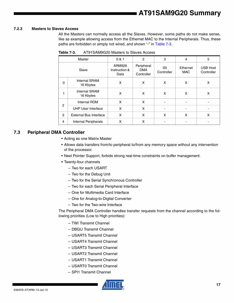
7.2.3 Masters to Slaves AccessAll the Masters can normally access all the Slaves. However, some paths do not make sense,like as example allowing access from the Ethernet MAC to the Internal Peripherals. Thus, thesepaths are forbidden or simply not wired, and shown “-” in Table 7-3.
7.3 Peripheral DMA Controller• Acting as one Matrix Master
• Allows data transfers from/to peripheral to/from any memory space without any intervention of the processor.
• Next Pointer Support, forbids strong real-time constraints on buffer management.
• Twenty-four channels
– Two for each USART
– Two for the Debug Unit
– Two for the Serial Synchronous Controller
– Two for each Serial Peripheral Interface
– One for Multimedia Card Interface
– One for Analog-to-Digital Converter
– Two for the Two-wire Interface
The Peripheral DMA Controller handles transfer requests from the channel according to the fol-lowing priorities (Low to High priorities):
– TWI Transmit Channel
– DBGU Transmit Channel
– USART5 Transmit Channel
– USART4 Transmit Channel
– USART3 Transmit Channel
– USART2 Transmit Channel
– USART1 Transmit Channel
– USART0 Transmit Channel
– SPI1 Transmit Channel
Table 7-3. AT91SAM9G20 Masters to Slaves Access
Master 0 & 1 2 3 4 5
SlaveARM926
Instruction & Data
Peripheral DMA
Controller
ISI Controller
Ethernet MAC
USB Host Controller
0Internal SRAM
16 KbytesX X X X X
1Internal SRAM
16 KbytesX X X X X
2Internal ROM X X - - -
UHP User Interface X X - - -
3 External Bus Interface X X X X X
4 Internal Peripherals X X - - -
176384DS–ATARM–13-Jan-10

– SPI0 Transmit Channel
– SSC Transmit Channel
– TWI Receive Channel
– DBGU Receive Channel
– USART5 Receive Channel
– USART4 Receive Channel
– USART3 Receive Channel
– USART2 Receive Channel
– USART1 Receive Channel
– USART0 Receive Channel
– ADC Receive Channel
– SPI1 Receive Channel
– SPI0 Receive Channel
– SSC Receive Channel
– MCI Transmit/Receive Channel
7.4 Debug and Test Features• ARM926 Real-time In-circuit Emulator
– Two real-time Watchpoint Units
– Two Independent Registers: Debug Control Register and Debug Status Register
– Test Access Port Accessible through JTAG Protocol
– Debug Communications Channel
• Debug Unit
– Two-pin UART
– Debug Communication Channel Interrupt Handling
– Chip ID Register
• IEEE1149.1 JTAG Boundary-scan on All Digital Pins
186384DS–ATARM–13-Jan-10
AT91SAM9G20 Summary

AT91SAM9G20 Summary
8. Memories
Figure 8-1. AT91SAM9G20 Memory Mapping
16K Bytes
16K Bytes
0xFFFC 000016K Bytes
0xFFFC 4000
SPI1
0xFFFC C000
SPI0
16K Bytes
0xFFFC 8000
16K Bytes
16K Bytes
16K Bytes
0xFFFA 4000TCO, TC1, TC2
0xFFFA 8000
MCI
0xFFFB 0000
0xFFFB 4000USART0
0xFFFB C000
USART1
0xFFFA 0000
0xFFFA C000
USART2
16K Bytes
TWI
16K Bytes
16K Bytes
0xFFFB 8000
16K Bytes
16K Bytes
UDP
SSC
256M Bytes
0x1000 0000
0x0000 0000
0x0FFF FFFF
0xFFFF FFFF
0xF000 00000xEFFF FFFF
Address Memory Space
Internal Peripherals
Internal Memories
EBIChip Select 0
EBIChip Select 1/
SDRAMC
EBIChip Select 2
EBIChip Select 3/NANDFlash
EBIChip Select 4/Compact Flash
Slot 0
EBIChip Select 5/Compact Flash
Slot 1
EBIChip Select 6
EBIChip Select 7
Undefined(Abort)
256M Bytes
256M Bytes
256M Bytes
256M Bytes
256M Bytes
256M Bytes
256M Bytes
1,518M Bytes
0x2000 00000x1FFF FFFF
0x3000 00000x2FFF FFFF
0x4000 00000x3FFF FFFF
0x6FFF FFFF
0x6000 00000x5FFF FFFF
0x5000 00000x4FFF FFFF
0x7000 0000
0x7FFF FFFF0x8000 0000
0x8FFF FFFF0x9000 0000
256M Bytes
0xFFFF FD00
0xFFFF FC00
0xFFFF FA00
0xFFFF F800
0xFFFF F600
0xFFFF F400
0xFFFF F200
16 Bytes
256 Bytes
512 bytes
512 bytes
512 Bytes
512 Bytes
PMC
PIOC
PIOB
PIOA
DBGU
RSTC
0xFFFF F000
512 BytesAIC
0xFFFF EE00
512 BytesMATRIX
0xFFFF EC00
512 BytesSMC
0xFFFF FD10 16 BytesSHDC
0xFFFF EA00
512 BytesSDRAMC
0xFFFF FD2016 BytesRTTC
0xFFFF FD3016 BytesPITC
0xFFFF FD4016 BytesWDTC
0xFFFF FD50 16 BytesGPBR0xFFFF FD60
Reserved
Reserved256M Bytes
Peripheral Mapping
Internal Memory Mapping(1) Can be ROM, EBI_NCS0 or SRAM
depending on BMS and REMAP
Notes :
ISI
EMAC
0xFFFF C000
SYSC Reserved0xFFFF FFFF
System Controller Mapping
16K Bytes
0xFFFF FFFF
Reserved
0xFFFF C000
ADC
USART3
USART4
USART5
TC3, TC4, TC5
16K Bytes
16K Bytes
16K Bytes
16K Bytes
16K Bytes
0xFFFD 4000
0xFFFD 8000
0xFFFD 0000
0xFFFE 0000
0xFFFD C000
0xFFFE 4000
0xFFFF E800
ECC 512 Bytes
CCFG0xFFFF EF10
32K Bytes
16K Bytes
0x10 8000
ROM
0x20 0000
SRAM0
0x30 0000
0x30 4000
SRAM1
0x50 4000
0x10 0000
0x20 4000
UHP
16K Bytes
16K Bytes
0x50 0000
Reserved
Reserved
Reserved
Reserved
0x0FFF FFFF
Boot Memory (1)0x0000 0000
Reserved0xF000 0000
196384DS–ATARM–13-Jan-10

A first level of address decoding is performed by the Bus Matrix, i.e., the implementation of theAdvanced High Performance Bus (AHB) for its Master and Slave interfaces with additionalfeatures.
Decoding breaks up the 4G bytes of address space into 16 banks of 256 Mbytes. The banks 1 to7 are directed to the EBI that associates these banks to the external chip selects EBI_NCS0 toEBI_NCS7. Bank 0 is reserved for the addressing of the internal memories, and a second levelof decoding provides 1 Mbyte of internal memory area. Bank 15 is reserved for the peripheralsand provides access to the Advanced Peripheral Bus (APB).
Other areas are unused and performing an access within them provides an abort to the masterrequesting such an access.
Each Master has its own bus and its own decoder, thus allowing a different memory mappingper Master. However, in order to simplify the mappings, all the masters have a similar addressdecoding.
Regarding Master 0 and Master 1 (ARM926 Instruction and Data), three different Slaves areassigned to the memory space decoded at address 0x0: one for internal boot, one for externalboot, one after remap. Refer to Table 8-1, “Internal Memory Mapping,” on page 20 for details.
A complete memory map is presented in Figure 8-1 on page 19.
8.1 Embedded Memories• 64-KByte ROM
– Single Cycle Access at full matrix speed
• Two 16-Kbyte Fast SRAM
– Single Cycle Access at full matrix speed
8.1.1 Boot StrategiesTable 8-1 summarizes the Internal Memory Mapping for each Master, depending on the Remapstatus and the BMS state at reset.
The system always boots at address 0x0. To ensure a maximum number of possibilities for boot,the memory layout can be configured with two parameters.
REMAP allows the user to lay out the first internal SRAM bank to 0x0 to ease development. Thisis done by software once the system has booted. When REMAP = 1, BMS is ignored. Refer tothe Bus Matrix Section for more details.
Table 8-1. Internal Memory Mapping
AddressREMAP = 0 REMAP = 1
BMS = 1 BMS = 0
0x0000 0000 ROM EBI_NCS0 SRAM0 16K
0x0010 0000 ROM
0x0020 0000 SRAM0 16K
0x0030 0000 SRAM1 16K
0x0050 0000 USB Host User Interface
206384DS–ATARM–13-Jan-10
AT91SAM9G20 Summary

AT91SAM9G20 Summary
When REMAP = 0, BMS allows the user to lay out to 0x0, at his convenience, the ROM or anexternal memory. This is done via hardware at reset.
Note: Memory blocks not affected by these parameters can always be seen at their specified base addresses. See the complete memory map presented in Figure 8-1 on page 19.
The AT91SAM9G20 matrix manages a boot memory that depends on the level on the BMS pinat reset. The internal memory area mapped between address 0x0 and 0x000F FFFF is reservedfor this purpose.
If BMS is detected at 1, the boot memory is the embedded ROM.
If BMS is detected at 0, the boot memory is the memory connected on the Chip Select 0 of theExternal Bus Interface.
8.1.1.1 BMS = 1, Boot on Embedded ROMThe system boots using the Boot Program.
• Boot on slow clock (On-chip RC or 32,768 Hz)
• Auto baudrate detection
• Downloads and runs an application from external storage media into internal SRAM
• Downloaded code size depends on embedded SRAM size
• Automatic detection of valid application
• Bootloader on a non-volatile memory
– SDCard (boot ROM does not support high capacity SDCards.)
– NAND Flash
– SPI DataFlash® and Serial Flash connected on NPCS0 and NPCS1 of the SPI0
– EEPROM on TWI
• SAM-BA® Boot in case no valid program is detected in external NVM, supporting
– Serial communication on a DBGU
– USB Device HS Port
8.1.1.2 BMS = 0, Boot on External Memory
• Boot on slow clock (On-chip RC or 32,768 Hz)
• Boot with the default configuration for the Static Memory Controller, byte select mode, 16-bit data bus, Read/Write controlled by Chip Select, allows boot on 16-bit non-volatile memory.
The customer-programmed software must perform a complete configuration.
To speed up the boot sequence when booting at 32 kHz EBI CS0 (BMS=0), the user must takethe following steps:
1. Program the PMC (main oscillator enable or bypass mode).
2. Program and start the PLL.
3. Reprogram the SMC setup, cycle, hold, mode timings registers for CS0 to adapt them to the new clock.
4. Switch the main clock to the new value.
216384DS–ATARM–13-Jan-10

8.2 External MemoriesThe external memories are accessed through the External Bus Interface. Each Chip Select linehas a 256-Mbyte memory area assigned.
Refer to the memory map in Figure 8-1 on page 19.
8.2.1 External Bus Interface
• Integrates three External Memory Controllers
– Static Memory Controller
– SDRAM Controller
– ECC Controller
• Additional logic for NAND Flash
• Full 32-bit External Data Bus
• Up to 26-bit Address Bus (up to 64MBytes linear)
• Up to 8 chip selects, Configurable Assignment:
– Static Memory Controller on NCS0
– SDRAM Controller or Static Memory Controller on NCS1
– Static Memory Controller on NCS2
– Static Memory Controller on NCS3, Optional NAND Flash support
– Static Memory Controller on NCS4 - NCS5, Optional CompactFlash support
– Static Memory Controller on NCS6-NCS7
8.2.2 Static Memory Controller
• 8-, 16- or 32-bit Data Bus
• Multiple Access Modes supported
– Byte Write or Byte Select Lines
– Asynchronous read in Page Mode supported (4- up to 32-byte page size)
• Multiple device adaptability
– Compliant with LCD Module
– Control signals programmable setup, pulse and hold time for each Memory Bank
• Multiple Wait State Management
– Programmable Wait State Generation
– External Wait Request
– Programmable Data Float Time
• Slow Clock mode supported
8.2.3 SDRAM Controller
• Supported devices
– Standard and Low-power SDRAM (Mobile SDRAM)
• Numerous configurations supported
– 2K, 4K, 8K Row Address Memory Parts
– SDRAM with two or four Internal Banks
– SDRAM with 16- or 32-bit Datapath
226384DS–ATARM–13-Jan-10
AT91SAM9G20 Summary
AT91SAM9G20 Summary
• Programming facilities
– Word, half-word, byte access
– Automatic page break when Memory Boundary has been reached
– Multibank Ping-pong Access
– Timing parameters specified by software
– Automatic refresh operation, refresh rate is programmable
• Energy-saving capabilities
– Self-refresh, power down and deep power down modes supported
• Error detection
– Refresh Error Interrupt
• SDRAM Power-up Initialization by software
• CAS Latency of 1, 2 and 3 supported
• Auto Precharge Command not used
8.2.4 Error Corrected Code Controller
• Hardware Error Corrected Code (ECC) Generation
– Detection and Correction by Software
• Supports NAND Flash and SmartMedia™ Devices with 8- or 16-bit Data Path.
• Supports NAND Flash/SmartMedia with Page Sizes of 528, 1056, 2112 and 4224 Bytes, Specified by Software
• Supports 1 bit correction for a page of 512,1024,2048 and 4096 Bytes with 8- or 16-bit Data Path
• Supports 1 bit correction per 512 bytes of data for a page size of 512, 2048 and 4096 Bytes with 8-bit Data Path
• Supports 1 bit correction per 256 bytes of data for a page size of 512, 2048 and 4096 Bytes with 8-bit Data Path
9. System ControllerThe System Controller is a set of peripherals, which allow handling of key elements of the sys-tem, such as power, resets, clocks, time, interrupts, watchdog, etc.
The System Controller User Interface embeds also the registers allowing to configure the Matrixand a set of registers for the chip configuration. The chip configuration registers allowsconfiguring:
– EBI chip select assignment and Voltage range for external memories
The System Controller’s peripherals are all mapped within the highest 16 Kbytes of addressspace, between addresses 0xFFFF E800 and 0xFFFF FFFF.
However, all the registers of System Controller are mapped on the top of the address space. Allthe registers of the System Controller can be addressed from a single pointer by using the stan-dard ARM instruction set, as the Load/Store instruction has an indexing mode of ±4 Kbytes.
Figure 9-1 on page 24 shows the System Controller block diagram.
Figure 8-1 on page 19 shows the mapping of the User Interfaces of the System Controllerperipherals.
236384DS–ATARM–13-Jan-10

9.1 System Controller Block Diagram
Figure 9-1. AT91SAM9G20 System Controller Block Diagram
NRST
SLCK
Advanced Interrupt Controller
Real-Time Timer
Periodic Interval Timer
Reset Controller
PA0-PA31
periph_nreset
System Controller
Watchdog Timer
wdt_faultWDRPROC
PIO Controllers
Power Management
Controller
XIN
XOUT
MAINCK
PLLACK
pit_irqMCK
proc_nreset
wdt_irq
periph_irq[2..4]periph_nreset
periph_clk[2..27]
PCK
MCK
pmc_irq
nirqnfiq
rtt_irq
EmbeddedPeripheralsperiph_clk[2..4]
pck[0-1]
inoutenable
ARM926EJ-S
SLCK
SLCK
irq0-irq2fiq
irq0-irq2fiq
periph_irq[6..24]
periph_irq[2..24]
int
int
periph_nreset
periph_clk[6..24]
jtag_nreset
por_ntrst
proc_nreset
periph_nreset
dbgu_txddbgu_rxd
pit_irq
dbgu_irqpmc_irq
rstc_irq
wdt_irq
rstc_irq
SLCK
Boundary Scan TAP Controller
jtag_nreset
debug
PCK
debugidle
debug
Bus Matrix
MCK
periph_nreset
proc_nreset
backup_nreset
periph_nreset
idle
Debug Unit
dbgu_irqMCK
dbgu_rxd
periph_nresetdbgu_txd
rtt_alarm
Shut-DownController
SLCK
rtt0_alarm
backup_nreset
SHDN
WKUP
4 General-PurposeBackup Registers
backup_nreset
XIN32
XOUT32
PLLBCK
PB0-PB31
PC0-PC31
VDDBU Powered
VDDCORE Powered
ntrst
VDDCOREPOR
MAINOSC
PLLA
VDDBUPOR
SLOWCLOCK
OSC
PLLB
por_ntrst
VDDBU
rtt_irq
UDPCK
USB Device
Port
UDPCK
periph_nreset
periph_clk[10]
periph_irq[10]
USB HostPortperiph_nreset
periph_clk[20]
periph_irq[20]
UHPCK
UHPCK
RC OSC
OSCSEL
246384DS–ATARM–13-Jan-10
AT91SAM9G20 Summary

AT91SAM9G20 Summary
9.2 Reset Controller• Based on two Power-on-Reset cell
– one on VDDBU and one on VDDCORE
• Status of the last reset
– Either general reset (VDDBU rising), wake-up reset (VDDCORE rising), software reset, user reset or watchdog reset
• Controls the internal resets and the NRST pin output
– Allows shaping a reset signal for the external devices
9.3 Shutdown Controller• Shutdown and Wake-Up logic
– Software programmable assertion of the SHDWN pin
– Deassertion Programmable on a WKUP pin level change or on alarm
9.4 Clock Generator• Embeds a Low Power 32768 Hz Slow Clock Oscillator and a Low power RC oscillator
selectable with OSCSEL signal
– Provides the permanent Slow Clock SLCK to the system
• Embeds the Main Oscillator
– Oscillator bypass feature
– Supports 3 to 20 MHz crystals
• Embeds 2 PLLs
– The PLL A outputs 400-800 MHz clock
– The PLL B outputs 100 MHz clock
– Both integrate an input divider to increase output accuracy
– PLL A and PLL B embed their own filters
256384DS–ATARM–13-Jan-10

Figure 9-2. Clock Generator Block Diagram
9.5 Power Management Controller• Provides:
– the Processor Clock PCK
– the Master Clock MCK, in particular to the Matrix and the memory interfaces.The MCK divider can be 1,2,4,6
– the USB Device Clock UDPCK
– independent peripheral clocks, typically at the frequency of MCK
– 2 programmable clock outputs: PCK0, PCK1
• Five flexible operating modes:
– Normal Mode, processor and peripherals running at a programmable frequency
– Idle Mode, processor stopped waiting for an interrupt
– Slow Clock Mode, processor and peripherals running at low frequency
– Standby Mode, mix of Idle and Backup Mode, peripheral running at low frequency, processor stopped waiting for an interrupt
– Backup Mode, Main Power Supplies off, VDDBU powered by a battery
On Chip RC OSC
Power Management
Controller
XIN
XOUT
Slow Clock SLCK
Main ClockMAINCK
PLLA ClockPLLACK
ControlStatus
PLL and Divider B
PLLB ClockPLLBCK
XIN32
XOUT32
Slow ClockOscillator
Main Oscillator
PLL and Divider A
Clock GeneratorOSCSEL
266384DS–ATARM–13-Jan-10
AT91SAM9G20 Summary

AT91SAM9G20 Summary
Figure 9-3. AT91SAM9G20 Power Management Controller Block Diagram
9.6 Periodic Interval Timer• Includes a 20-bit Periodic Counter, with less than 1 µs accuracy
• Includes a 12-bit Interval Overlay Counter
• Real Time OS or Linux®/Windows CE® compliant tick generator
9.7 Watchdog Timer• 16-bit key-protected only-once-Programmable Counter
• Windowed, prevents the processor being in a dead-lock on the watchdog access
9.8 Real-time Timer• Real-time Timer 32-bit free-running back-up Counter
• Integrates a 16-bit programmable prescaler running on slow clock
• Alarm Register capable of generating a wake-up of the system through the Shutdown Controller
9.9 General-purpose Back-up Registers• Four 32-bit backup general-purpose registers
9.10 Advanced Interrupt Controller• Controls the interrupt lines (nIRQ and nFIQ) of the ARM Processor
• Thirty-two individually maskable and vectored interrupt sources
MCK
periph_clk[..]
int
SLCKMAINCKPLLACK
Prescaler/1,/2,/4,.../64
PCKProcessor
Clock Controller
Idle ModeMaster Clock Controller
PeripheralsClock Controller
ON/OFF
PLLBCK
Divider/1,/2,/4,/6
USB Clock Controller
SLCKMAINCKPLLACK
Prescaler/1,/2,/4,...,/64
Programmable Clock Controller
PLLBCK Divider/1,/2,/4
pck[..]
PLLBCK
UDPCKON/OFF
ON/OFF
/1,/2Divider
276384DS–ATARM–13-Jan-10

– Source 0 is reserved for the Fast Interrupt Input (FIQ)
– Source 1 is reserved for system peripherals
– Programmable Edge-triggered or Level-sensitive Internal Sources
– Programmable Positive/Negative Edge-triggered or High/Low Level-sensitive
• Three External Sources plus the Fast Interrupt signal
• 8-level Priority Controller
– Drives the Normal Interrupt of the processor
– Handles priority of the interrupt sources 1 to 31
– Higher priority interrupts can be served during service of lower priority interrupt
• Vectoring
– Optimizes Interrupt Service Routine Branch and Execution
– One 32-bit Vector Register per interrupt source
– Interrupt Vector Register reads the corresponding current Interrupt Vector
• Protect Mode
– Easy debugging by preventing automatic operations when protect models are enabled
• Fast Forcing
– Permits redirecting any normal interrupt source on the Fast Interrupt of the processor
9.11 Debug Unit• Composed of two functions:
– Two-pin UART
– Debug Communication Channel (DCC) support
• Two-pin UART
– Implemented features are 100% compatible with the standard Atmel ® USART
– Independent receiver and transmitter with a common programmable Baud Rate Generator
– Even, Odd, Mark or Space Parity Generation
– Parity, Framing and Overrun Error Detection
– Automatic Echo, Local Loopback and Remote Loopback Channel Modes
– Support for two PDC channels with connection to receiver and transmitter
• Debug Communication Channel Support
– Offers visibility of and interrupt trigger from COMMRX and COMMTX signals from the ARM Processor’s ICE Interface
9.12 Chip Identification• Chip ID:0x019905A1
• JTAG ID: 0x05B2403F
• ARM926 TAP ID:0x0792603F
286384DS–ATARM–13-Jan-10
AT91SAM9G20 Summary

AT91SAM9G20 Summary
10. Peripherals
10.1 User InterfaceThe peripherals are mapped in the upper 256 Mbytes of the address space between theaddresses 0xFFFA 0000 and 0xFFFC FFFF. Each User Peripheral is allocated 16 Kbytes ofaddress space. A complete memory map is presented in Figure 8-1 on page 19.
10.2 IdentifiersTable 10-1 defines the Peripheral Identifiers of the AT91SAM9G20. A peripheral identifier isrequired for the control of the peripheral interrupt with the Advanced Interrupt Controller and forthe control of the peripheral clock with the Power Management Controller.
Table 10-1. AT91SAM9G20 Peripheral Identifiers (Continued)
Peripheral ID Peripheral Mnemonic Peripheral Name External Interrupt
0 AIC Advanced Interrupt Controller FIQ
1 SYSC System Controller Interrupt
2 PIOA Parallel I/O Controller A
3 PIOB Parallel I/O Controller B
4 PIOC Parallel I/O Controller C
5 ADC Analog to Digital Converter
6 US0 USART 0
7 US1 USART 1
8 US2 USART 2
9 MCI Multimedia Card Interface
10 UDP USB Device Port
11 TWI Two-wire Interface
12 SPI0 Serial Peripheral Interface 0
13 SPI1 Serial Peripheral Interface 1
14 SSC Synchronous Serial Controller
15 - Reserved
16 - Reserved
17 TC0 Timer/Counter 0
18 TC1 Timer/Counter 1
19 TC2 Timer/Counter 2
20 UHP USB Host Port
21 EMAC Ethernet MAC
22 ISI Image Sensor Interface
23 US3 USART 3
24 US4 USART 4
25 US5 USART 5
26 TC3 Timer/Counter 3
27 TC4 Timer/Counter 4
28 TC5 Timer/Counter 5
296384DS–ATARM–13-Jan-10

Note: Setting AIC, SYSC, UHP, ADC and IRQ0-2 bits in the clock set/clear registers of the PMC has no effect. The ADC clock is auto-matically started for the first conversion. In Sleep Mode the ADC clock is automatically stopped after each conversion.
10.2.1 Peripheral Interrupts and Clock Control
10.2.1.1 System InterruptThe System Interrupt in Source 1 is the wired-OR of the interrupt signals coming from:
• the SDRAM Controller
• the Debug Unit
• the Periodic Interval Timer
• the Real-time Timer
• the Watchdog Timer
• the Reset Controller
• the Power Management Controller
The clock of these peripherals cannot be deactivated and Peripheral ID 1 can only be usedwithin the Advanced Interrupt Controller.
10.2.1.2 External InterruptsAll external interrupt signals, i.e., the Fast Interrupt signal FIQ or the Interrupt signals IRQ0 toIRQ2, use a dedicated Peripheral ID. However, there is no clock control associated with theseperipheral IDs.
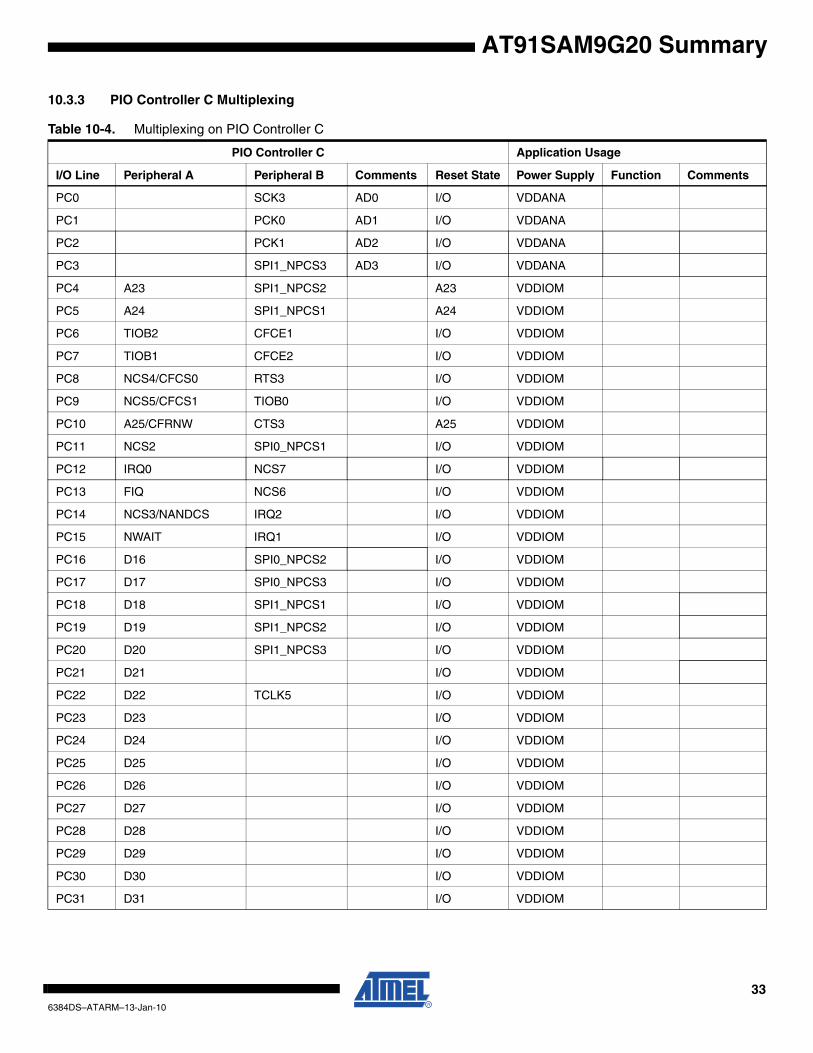
10.3 Peripheral Signal Multiplexing on I/O LinesThe AT91SAM9G20 features 3 PIO controllers (PIOA, PIOB, PIOC) that multiplex the I/O linesof the peripheral set.
Each PIO Controller controls up to 32 lines. Each line can be assigned to one of two peripheralfunctions, A or B. Table 10-2 on page 31, Table 10-3 on page 32 and Table 10-4 on page 33define how the I/O lines of the peripherals A and B are multiplexed on the PIO Controllers. Thetwo columns “Function” and “Comments” have been inserted in this table for the user’s owncomments; they may be used to track how pins are defined in an application.
Note that some peripheral functions which are output only might be duplicated within bothtables.
The column “Reset State” indicates whether the PIO Line resets in I/O mode or in peripheralmode. If I/O appears, the PIO Line resets in input with the pull-up enabled, so that the device ismaintained in a static state as soon as the reset is released. As a result, the bit corresponding tothe PIO Line in the register PIO_PSR (Peripheral Status Register) resets low.
If a signal name appears in the “Reset State” column, the PIO Line is assigned to this functionand the corresponding bit in PIO_PSR resets high. This is the case of pins controlling memories,in particular the address lines, which require the pin to be driven as soon as the reset isreleased. Note that the pull-up resistor is also enabled in this case.
29 AIC Advanced Interrupt Controller IRQ0
30 AIC Advanced Interrupt Controller IRQ1
31 AIC Advanced Interrupt Controller IRQ2
Table 10-1. AT91SAM9G20 Peripheral Identifiers (Continued)
Peripheral ID Peripheral Mnemonic Peripheral Name External Interrupt
306384DS–ATARM–13-Jan-10
AT91SAM9G20 Summary

AT91SAM9G20 Summary
10.3.1 PIO Controller A Multiplexing
Table 10-2. Multiplexing on PIO Controller A
PIO Controller A Application Usage
I/O Line Peripheral A Peripheral B Comments Reset State Power Supply Function Comments
PA0 SPI0_MISO MCDB0 I/O VDDIOP
PA1 SPI0_MOSI MCCDB I/O VDDIOP
PA2 SPI0_SPCK I/O VDDIOP
PA3 SPI0_NPCS0 MCDB3 I/O VDDIOP
PA4 RTS2 MCDB2 I/O VDDIOP
PA5 CTS2 MCDB1 I/O VDDIOP
PA6 MCDA0 I/O VDDIOP
PA7 MCCDA I/O VDDIOP
PA8 MCCK I/O VDDIOP
PA9 MCDA1 I/O VDDIOP
PA10 MCDA2 ETX2 I/O VDDIOP
PA11 MCDA3 ETX3 I/O VDDIOP
PA12 ETX0 I/O VDDIOP
PA13 ETX1 I/O VDDIOP
PA14 ERX0 I/O VDDIOP
PA15 ERX1 I/O VDDIOP
PA16 ETXEN I/O VDDIOP
PA17 ERXDV I/O VDDIOP
PA18 ERXER I/O VDDIOP
PA19 ETXCK I/O VDDIOP
PA20 EMDC I/O VDDIOP
PA21 EMDIO I/O VDDIOP
PA22 ADTRG ETXER I/O VDDIOP
PA23 TWD ETX2 I/O VDDIOP
PA24 TWCK ETX3 I/O VDDIOP
PA25 TCLK0 ERX2 I/O VDDIOP
PA26 TIOA0 ERX3 I/O VDDIOP
PA27 TIOA1 ERXCK I/O VDDIOP
PA28 TIOA2 ECRS I/O VDDIOP
PA29 SCK1 ECOL I/O VDDIOP
PA30 SCK2 RXD4 I/O VDDIOP
PA31 SCK0 TXD4 I/O VDDIOP
316384DS–ATARM–13-Jan-10
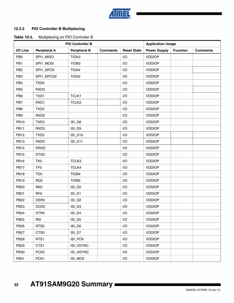
10.3.2 PIO Controller B Multiplexing
Table 10-3. Multiplexing on PIO Controller B
PIO Controller B Application Usage
I/O Line Peripheral A Peripheral B Comments Reset State Power Supply Function Comments
PB0 SPI1_MISO TIOA3 I/O VDDIOP
PB1 SPI1_MOSI TIOB3 I/O VDDIOP
PB2 SPI1_SPCK TIOA4 I/O VDDIOP
PB3 SPI1_NPCS0 TIOA5 I/O VDDIOP
PB4 TXD0 I/O VDDIOP
PB5 RXD0 I/O VDDIOP
PB6 TXD1 TCLK1 I/O VDDIOP
PB7 RXD1 TCLK2 I/O VDDIOP
PB8 TXD2 I/O VDDIOP
PB9 RXD2 I/O VDDIOP
PB10 TXD3 ISI_D8 I/O VDDIOP
PB11 RXD3 ISI_D9 I/O VDDIOP
PB12 TXD5 ISI_D10 I/O VDDIOP
PB13 RXD5 ISI_D11 I/O VDDIOP
PB14 DRXD I/O VDDIOP
PB15 DTXD I/O VDDIOP
PB16 TK0 TCLK3 I/O VDDIOP
PB17 TF0 TCLK4 I/O VDDIOP
PB18 TD0 TIOB4 I/O VDDIOP
PB19 RD0 TIOB5 I/O VDDIOP
PB20 RK0 ISI_D0 I/O VDDIOP
PB21 RF0 ISI_D1 I/O VDDIOP
PB22 DSR0 ISI_D2 I/O VDDIOP
PB23 DCD0 ISI_D3 I/O VDDIOP
PB24 DTR0 ISI_D4 I/O VDDIOP
PB25 RI0 ISI_D5 I/O VDDIOP
PB26 RTS0 ISI_D6 I/O VDDIOP
PB27 CTS0 ISI_D7 I/O VDDIOP
PB28 RTS1 ISI_PCK I/O VDDIOP
PB29 CTS1 ISI_VSYNC I/O VDDIOP
PB30 PCK0 ISI_HSYNC I/O VDDIOP
PB31 PCK1 ISI_MCK I/O VDDIOP
326384DS–ATARM–13-Jan-10
AT91SAM9G20 Summary
AT91SAM9G20 Summary
10.3.3 PIO Controller C Multiplexing
Table 10-4. Multiplexing on PIO Controller C
PIO Controller C Application Usage
I/O Line Peripheral A Peripheral B Comments Reset State Power Supply Function Comments
PC0 SCK3 AD0 I/O VDDANA
PC1 PCK0 AD1 I/O VDDANA
PC2 PCK1 AD2 I/O VDDANA
PC3 SPI1_NPCS3 AD3 I/O VDDANA
PC4 A23 SPI1_NPCS2 A23 VDDIOM
PC5 A24 SPI1_NPCS1 A24 VDDIOM
PC6 TIOB2 CFCE1 I/O VDDIOM
PC7 TIOB1 CFCE2 I/O VDDIOM
PC8 NCS4/CFCS0 RTS3 I/O VDDIOM
PC9 NCS5/CFCS1 TIOB0 I/O VDDIOM
PC10 A25/CFRNW CTS3 A25 VDDIOM
PC11 NCS2 SPI0_NPCS1 I/O VDDIOM
PC12 IRQ0 NCS7 I/O VDDIOM
PC13 FIQ NCS6 I/O VDDIOM
PC14 NCS3/NANDCS IRQ2 I/O VDDIOM
PC15 NWAIT IRQ1 I/O VDDIOM
PC16 D16 SPI0_NPCS2 I/O VDDIOM
PC17 D17 SPI0_NPCS3 I/O VDDIOM
PC18 D18 SPI1_NPCS1 I/O VDDIOM
PC19 D19 SPI1_NPCS2 I/O VDDIOM
PC20 D20 SPI1_NPCS3 I/O VDDIOM
PC21 D21 I/O VDDIOM
PC22 D22 TCLK5 I/O VDDIOM
PC23 D23 I/O VDDIOM
PC24 D24 I/O VDDIOM
PC25 D25 I/O VDDIOM
PC26 D26 I/O VDDIOM
PC27 D27 I/O VDDIOM
PC28 D28 I/O VDDIOM
PC29 D29 I/O VDDIOM
PC30 D30 I/O VDDIOM
PC31 D31 I/O VDDIOM
336384DS–ATARM–13-Jan-10
10.4 Embedded Peripherals
10.4.1 Serial Peripheral Interface
• Supports communication with serial external devices
– Four chip selects with external decoder support allow communication with up to 15 peripherals
– Serial memories, such as DataFlash and 3-wire EEPROMs
– Serial peripherals, such as ADCs, DACs, LCD Controllers, CAN Controllers and Sensors
– External co-processors
• Master or slave serial peripheral bus interface
– 8- to 16-bit programmable data length per chip select
– Programmable phase and polarity per chip select
– Programmable transfer delays between consecutive transfers and between clock and data per chip select
– Programmable delay between consecutive transfers
– Selectable mode fault detection
• Very fast transfers supported
– Transfers with baud rates up to MCK
– The chip select line may be left active to speed up transfers on the same device
10.4.2 Two-wire Interface
• Compatibility with standard two-wire serial memory
• One, two or three bytes for slave address
• Sequential read/write operations
• Supports either master or slave modes
• Compatible with standard two-wire serial memories
• Master, multi-master and slave mode operation
• Bit rate: up to 400 Kbits
• General Call supported in slave mode
• Connection to Peripheral DMA Controller (PDC) capabilities optimizes data transfers in master mode only
– One channel for the receiver, one channel for the transmitter
– Next buffer support
10.4.3 USART
• Programmable Baud Rate Generator
• 5- to 9-bit full-duplex synchronous or asynchronous serial communications
– 1, 1.5 or 2 stop bits in Asynchronous Mode or 1 or 2 stop bits in Synchronous Mode
– Parity generation and error detection
– Framing error detection, overrun error detection
– MSB- or LSB-first
– Optional break generation and detection
346384DS–ATARM–13-Jan-10
AT91SAM9G20 Summary

AT91SAM9G20 Summary
– By 8 or by-16 over-sampling receiver frequency
– Hardware handshaking RTS-CTS
– Optional modem signal management DTR-DSR-DCD-RI
– Receiver time-out and transmitter timeguard
– Optional Multi-drop Mode with address generation and detection
– Optional Manchester Encoding
• RS485 with driver control signal
• ISO7816, T = 0 or T = 1 Protocols for interfacing with smart cards
– NACK handling, error counter with repetition and iteration limit
• IrDA modulation and demodulation
– Communication at up to 115.2 Kbps
• Test Modes
– Remote Loopback, Local Loopback, Automatic Echo
The USART contains features allowing management of the Modem Signals DTR, DSR, DCDand RI. In the AT91SAM9G20, only the USART0 implements these signals, named DTR0,DSR0, DCD0 and RI0.
The USART1 and USART2 do not implement all the modem signals. Only RTS and CTS (RTS1and CTS1, RTS2 and CTS2, respectively) are implemented in these USARTs for other features.
Thus, programming the USART1, USART2 or the USART3 in Modem Mode may lead to unpre-dictable results. In these USARTs, the commands relating to the Modem Mode have no effectand the status bits relating the status of the modem signals are never activated.
10.4.4 Serial Synchronous Controller
• Provides serial synchronous communication links used in audio and telecom applications (with CODECs in Master or Slave Modes, I2S, TDM Buses, Magnetic Card Reader, etc.)
• Contains an independent receiver and transmitter and a common clock divider
• Offers a configurable frame sync and data length
• Receiver and transmitter can be programmed to start automatically or on detection of different event on the frame sync signal
• Receiver and transmitter include a data signal, a clock signal and a frame synchronization signal
10.4.5 Timer Counter
• Two blocks of three 16-bit Timer Counter channels
• Each channel can be individually programmed to perform a wide range of functions including:
– Frequency Measurement
– Event Counting
– Interval Measurement
– Pulse Generation
– Delay Timing
– Pulse Width Modulation
– Up/down Capabilities
• Each channel is user-configurable and contains:
356384DS–ATARM–13-Jan-10

– Three external clock inputs
– Five internal clock inputs
– Two multi-purpose input/output signals
• Each block contains two global registers that act on all three TC Channels
Note: TC Block 0 (TC0, TC1, TC2) and TC Block 1 (TC3, TC4, TC5) have identical user interfaces. See Figure 8-1, “AT91SAM9G20 Memory Mapping,” on page 19 for TC Block 0 and TC Block 1 base addresses.
10.4.6 Multimedia Card Interface
• One double-channel MultiMedia Card Interface
• Compatibility with MultiMedia Card Specification Version 3.11
• Compatibility with SD Memory Card Specification Version 1.1
• Compatibility with SDIO Specification Version V1.0.
• Card clock rate up to Master Clock divided by 2
• Embedded power management to slow down clock rate when not used
• MCI has two slots, each supporting
– One slot for one MultiMediaCard bus (up to 30 cards) or
– One SD Memory Card
• Support for stream, block and multi-block data read and write
10.4.7 USB Host Port
• Compliance with Open HCI Rev 1.0 Specification
• Compliance with USB V2.0 Full-speed and Low-speed Specification
• Supports both Low-Speed 1.5 Mbps and Full-speed 12 Mbps devices
• Root hub integrated with two downstream USB ports in the 217-LFBGA package
• Two embedded USB transceivers
• Supports power management
• Operates as a master on the Matrix
10.4.8 USB Device Port
• USB V2.0 full-speed compliant, 12 MBits per second
• Embedded USB V2.0 full-speed transceiver
• Embedded 2,432-byte dual-port RAM for endpoints
• Suspend/Resume logic
• Ping-pong mode (two memory banks) for isochronous and bulk endpoints
• Six general-purpose endpoints
– Endpoint 0 and 3: 64 bytes, no ping-pong mode
– Endpoint 1 and 2: 64 bytes, ping-pong mode
– Endpoint 4 and 5: 512 bytes, ping-pong mode
• Embedded pad pull-up
366384DS–ATARM–13-Jan-10
AT91SAM9G20 Summary
AT91SAM9G20 Summary
10.4.9 Ethernet 10/100 MAC
• Compatibility with IEEE Standard 802.3
• 10 and 100 MBits per second data throughput capability
• Full- and half-duplex operations
• MII or RMII interface to the physical layer
• Register Interface to address, data, status and control registers
• DMA Interface, operating as a master on the Memory Controller
• Interrupt generation to signal receive and transmit completion
• 28-byte transmit and 28-byte receive FIFOs
• Automatic pad and CRC generation on transmitted frames
• Address checking logic to recognize four 48-bit addresses
• Support promiscuous mode where all valid frames are copied to memory
• Support physical layer management through MDIO interface
10.4.10 Image Sensor Interface
• ITU-R BT. 601/656 8-bit mode external interface support
• Support for ITU-R BT.656-4 SAV and EAV synchronization
• Vertical and horizontal resolutions up to 2048 x 2048
• Preview Path up to 640 x 480 in RGMB mode, 2048 x2048 in grayscale mode
• Support for packed data formatting for YCbCr 4:2:2 formats
• Preview scaler to generate smaller size image
• Programmable frame capture rate
10.4.11 Analog-to-Digital Converter
• 4-channel ADC
• 10-bit 312K samples/sec. Successive Approximation Register ADC
• -2/+2 LSB Integral Non Linearity, -1/+1 LSB Differential Non Linearity
• Individual enable and disable of each channel
• External voltage reference for better accuracy on low voltage inputs
• Multiple trigger source – Hardware or software trigger – External trigger pin – Timer Counter 0 to 2 outputs TIOA0 to TIOA2 trigger
• Sleep Mode and conversion sequencer – Automatic wakeup on trigger and back to sleep mode after conversions of all enabled channels
• Four analog inputs shared with digital signals
376384DS–ATARM–13-Jan-10
11. Pacakge Drawing
11.1 217-ball LFBA Package
Figure 11-1. 217-ball LFBGA Package Drawing
386384DS–ATARM–13-Jan-10
AT91SAM9G20 Summary

AT91SAM9G20 Summary
11.2 247-ball TFBGA Package
Figure 11-2. 247-ball TFBGA Package Drawing
396384DS–ATARM–13-Jan-10
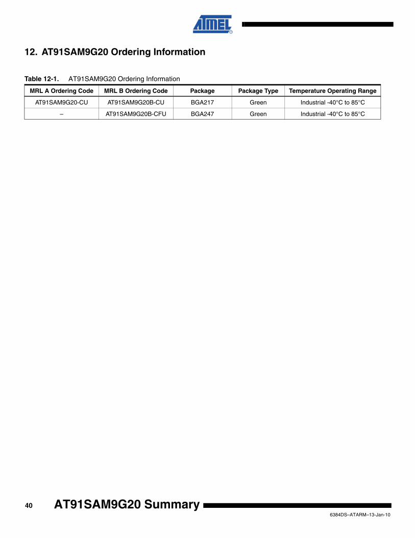
12. AT91SAM9G20 Ordering Information
Table 12-1. AT91SAM9G20 Ordering Information
MRL A Ordering Code MRL B Ordering Code Package Package Type Temperature Operating Range
AT91SAM9G20-CU AT91SAM9G20B-CU BGA217 Green Industrial -40°C to 85°C
– AT91SAM9G20B-CFU BGA247 Green Industrial -40°C to 85°C
406384DS–ATARM–13-Jan-10
AT91SAM9G20 Summary

AT91SAM9G20 Summary
Revision History
Doc. Rev CommentsChange Request Ref.
6348DS Section 5. “Power Considerations”, removed subsection: “Power Consumption
Section 6. “I/O Line Considerations”, removed subsection: Slow Clock Selection6945
6348CS “Features” , Section 4.3 “247-ball TFBGA Package Outline”, Section 4.4 “247-ball TFBGA Package Pinout”, added 247-ball TFBGA package information.
6079
Section 10.4.6 “Multimedia Card Interface”, compatibility with MultiMedia Card spec v3.11, SD Memory Card spec v1.1.
6080
Signal Description, Table 3-1, added GNDPLL to table 6022
Table 3-1, Signal Description and Section 10-4 “Multiplexing on PIO Controller C”, EF100 removed. 6148
Section 11. “Pacakge Drawing”:Section 11.2 “247-ball TFBGA Package”, added to summary. 6079
Section 12. “AT91SAM9G20 Ordering Information”Table 12-1, “AT91SAM9G20 Ordering Information,” MLR B ordering information added to summary. 6079
6384BS Overview“Features” on page 1, Debug Unit (DBGU) updated.
Section 10.4.3 “USART”, “Optional Manchester Encoding” added to list of USART features.Section 8.1.1.1 “BMS = 1, Boot on Embedded ROM”, – SDCard, (boot ROM does not support high capacity SDCards) clarification added.
5846
59315935
Section 6.6 “Shutdown Logic Pins”, updated with external pull-up requirement. rfo
6384AS First issue
416384DS–ATARM–13-Jan-10

Headquarters International
Atmel Corporation2325 Orchard ParkwaySan Jose, CA 95131USATel: 1(408) 441-0311Fax: 1(408) 487-2600
Atmel AsiaUnit 1-5 & 16, 19/FBEA Tower, Millennium City 5418 Kwun Tong RoadKwun Tong, KowloonHong KongTel: (852) 2245-6100Fax: (852) 2722-1369
Atmel EuropeLe Krebs8, Rue Jean-Pierre TimbaudBP 30978054 Saint-Quentin-en-Yvelines CedexFranceTel: (33) 1-30-60-70-00 Fax: (33) 1-30-60-71-11
Atmel Japan9F, Tonetsu Shinkawa Bldg.1-24-8 ShinkawaChuo-ku, Tokyo 104-0033JapanTel: (81) 3-3523-3551Fax: (81) 3-3523-7581
Product Contact
Web Sitewww.atmel.comwww.atmel.com/AT91SAM
Technical SupportAT91SAM SupportAtmel techincal support
Sales Contactswww.atmel.com/contacts/
Literature Requestswww.atmel.com/literature
Disclaimer: The information in this document is provided in connection with Atmel products. No license, express or implied, by estoppel or otherwise, to anyintellectual property right is granted by this document or in connection with the sale of Atmel products. EXCEPT AS SET FORTH IN ATMEL’S TERMS AND CONDI-TIONS OF SALE LOCATED ON ATMEL’S WEB SITE, ATMEL ASSUMES NO LIABILITY WHATSOEVER AND DISCLAIMS ANY EXPRESS, IMPLIED OR STATUTORYWARRANTY RELATING TO ITS PRODUCTS INCLUDING, BUT NOT LIMITED TO, THE IMPLIED WARRANTY OF MERCHANTABILITY, FITNESS FOR A PARTICULARPURPOSE, OR NON-INFRINGEMENT. IN NO EVENT SHALL ATMEL BE LIABLE FOR ANY DIRECT, INDIRECT, CONSEQUENTIAL, PUNITIVE, SPECIAL OR INCIDEN-TAL DAMAGES (INCLUDING, WITHOUT LIMITATION, DAMAGES FOR LOSS OF PROFITS, BUSINESS INTERRUPTION, OR LOSS OF INFORMATION) ARISING OUTOF THE USE OR INABILITY TO USE THIS DOCUMENT, EVEN IF ATMEL HAS BEEN ADVISED OF THE POSSIBILITY OF SUCH DAMAGES. Atmel makes norepresentations or warranties with respect to the accuracy or completeness of the contents of this document and reserves the right to make changes to specificationsand product descriptions at any time without notice. Atmel does not make any commitment to update the information contained herein. Unless specifically providedotherwise, Atmel products are not suitable for, and shall not be used in, automotive applications. Atmel’s products are not intended, authorized, or warranted for useas components in applications intended to support or sustain life.
© 2010 Atmel Corporation. All rights reserved. Atmel®, logo and combinations thereof DataFlash®, SAM-BA® and others are registered trade-marks or trademarks of Atmel Corporation or its subsidiaries. ARM®, Thumb® and the ARMPowered logo® and others are registered trademarksor trademarks ARM Ltd. Windows® and others are registered trademarks or trademarks of Microsoft Corporation in the US and/or other coun-tries. Other terms and product names may be trademarks of others.
6384DS–ATARM–13-Jan-10