ARM Introduction & Instruction Set Architecturemilenka/cpe626-04F/secure/l18_arm_3p1.pdf7 ARM...
24
ARM Introduction & Instruction Set Architecture Aleksandar Milenkovic E-mail: [email protected] Web: http://www.ece.uah.edu/~milenka 2 Outline ARM Architecture ARM Organization and Implementation ARM Instruction Set Thumb Instruction Set Architectural Support for System Development ARM Processor Cores Memory Hierarchy Architectural Support for Operating Systems ARM CPU Cores Embedded ARM Applications 3 ARM History ARM – Acorn RISC Machine (1983 – 1985) § Acorn Computers Limited, Cambridge, England ARM – Advanced RISC Machine 1990 § ARM Limited, 1990 § ARM has been licensed to many semiconductor manufacturers
Transcript of ARM Introduction & Instruction Set Architecturemilenka/cpe626-04F/secure/l18_arm_3p1.pdf7 ARM...

ARMIntroduction &
Instruction Set Architecture
Aleksandar MilenkovicE-mail: [email protected]: http://www. ece.uah.edu/~milenka
2
OutlineØ ARM ArchitectureØ ARM Organization and Implementation
Ø ARM Instruction SetØ Thumb Instruction Set
Ø Architectural Support for System DevelopmentØ ARM Processor Cores
Ø Memory HierarchyØ Architectural Support for Operating Systems
Ø ARM CPU CoresØ Embedded ARM Applications
3
ARM HistoryØ ARM – Acorn RISC Machine (1983 – 1985)§ Acorn Computers Limited, Cambridge, England
Ø ARM – Advanced RISC Machine 1990 § ARM Limited, 1990§ ARM has been licensed to many semiconductor
manufacturers
4
ARM’s visible registersØ User level§ 15 GPRs, PC,
CPSR (current program status register)
Ø Remaining registers are used for system-level programming and for handling exceptions
r13_und r14_und r14_ irq
r13_ irq
SPSR_und
r14_ abt r14_svc
user mode fiqmode
svcmode
abortmode
irqmode
undefinedmode
usable in user mode
system modes only
r13_ abt r13_svc
r8_fiqr9_fiq
r10_ fiqr11_fiq
SPSR_irq SPSR_abt SPSR_svc SPSR_fiqCPSR
r14_ fiqr13_ fiqr12_ fiq
r0r1r2r3r4r5r6r7r8r9r10r11r12r13r14r15 (PC)
5
ARM CPSR formatØ N (Negative), Z (Zero), C (Carry), V (oVerflow )Ø mode – control processor mode
Ø T – control instruction set§ T = 1 – instruction stream is 16-bit Thumb instructions§ T = 0 – instruction stream is 32-bit ARM instructions
Ø I F – interrupt enables
N Z C V unused mode
31 2827 8 7 6 5 4 0
I F T
6
ARM memory organizationØ Linear array of bytes numbered from 0
to 232 – 1Ø Data items§ bytes (8 bits)§ half-words (16 bits) – always
aligned to 2-byte boundaries (start at an even byte address)
§ words (32 bits) – always aligned to 4-byte boundaries (start at a byte address which is multiple of 4)
half-word4
word16
0123
4567
891011
byte0byte
12131415
16171819
20212223
byte1byte2
half-word14
byte3
byte6
address
bit 31 bit 0
half-word12
word8

7
ARM instruction setØ Load-store architecture§ operands are in GPRs§ load/store – only instructions that operate with memory
Ø Instructions§ Data Processing – use and change only register values§ Data Transfer – copy memory values into registers (load) or
copy register values into memory (store)§ Control Flow
o branch o branch-and-link –
save return address to resume the original sequenceo trapping into system code – supervisor calls
8
ARM instruction set (cont’d)Ø Three-address data processing instructionsØ Conditional execution of every instruction
Ø Powerful load/store multiple register instructionsØ Ability to perform a general shift operation and a general
ALU operation in a single instruction that executes in a single clock cycle
Ø Open instruction set extension through coprocessor instruction set, including adding new registers and data types to the programmer’s model
Ø Very dense 16-bit compressed representation of the instruction set in the Thumb architecture
9
I/O systemØ I/O is memory mapped § internal registers of peripherals (disk controllers, network
interfaces, etc) are addressable locations within the ARM’s memory map and may be read and written using the load-store instructions
Ø Peripherals may use either the normal interrupt (IRQ) or fast interrupt (FIQ) input§ normally most interrupt sources share the IRQ input, while
just one or two time-critical sources are connected to the FIQ input
Ø Some systems may include external DMA hardware to handle high-bandwidth I/O traffic

10
ARM exceptionsØ ARM supports a range of interrupts, traps, and supervisor calls – all
are grouped under the general heading of exceptionsØ Handling exceptions§ current state is saved by copying the PC into r14_exc and CPSR
into SPSR_exc (exc stands for exception type)§ processor operating mode is changed to the appropriate exception
mode§ PC is forced to a value between 0016 and 1C16, the particular value
depending on the type of exception § instruction at the location PC is forced to (the vector address)
usually contains a branch to the exception handler; the exception handler will use r13_exc, which is normally initialized to point to a dedicated stack in memory, to save some user registers
§ return: restore the user registers and then restore PC and CPSRatomically
11
ARM cross-development toolkitØ Software development§ tools developed by ARM
Limited§ public domain tools
(ARM back end for gcc C compiler)
Ø Cross-development§ tools run on different
architecture from one for which they produce code
assemblerC compiler
C source asmsource
.aof
C libraries
linker
.axf
ARMsd
debug
ARMulator development
system model
board
objectlibraries
12
OutlineØ ARM ArchitectureØ ARM Assembly Language ProgrammingØ ARM Organization and ImplementationØ ARM Instruction SetØ Architectural Support for High-level LanguagesØ Thumb Instruction SetØ Architectural Support for System DevelopmentØ ARM Processor CoresØ Memory HierarchyØ Architectural Support for Operating SystemsØ ARM CPU CoresØ Embedded ARM Applications

13
ARM Instruction SetØ Data Processing InstructionsØ Data Transfer Instructions
Ø Control flow Instructions
14
Data Processing InstructionsØ Classes of data processing instructions§ Arithmetic operations§ Bit-wise logical operations§ Register-movement operations§ Comparison operations
Ø Operands: 32-bits wide;there are 3 ways to specify operands§ come from registers§ the second operand may be a constant (immediate)§ shifted register operand
Ø Result: 32-bits wide, placed in a register§ long multiply produces a 64-bit result
15
Data Processing Instructions (cont’d)
r0 := r2 – r1 + C - 1RSC r0, r1, r2
r0 := r1 - r2SUB r0, r1, r2r0 := r1 - r2 + C - 1SBC r0, r1, r2r0 := r2 – r1RSB r0, r1, r2
r0 := r1 + r2 + CADC r0, r1, r2r0 := r1 + r2ADD r0, r1, r2
Arithmetic Operations Bit-wise Logical Operations
r0 := r1 xor r2EOR r0, r1, r2r0 := r1 and (not) r2BIC r0, r1, r2
r0 := r1 or r2ORR r0, r1, r2r0 := r1 and r2AND r0, r1, r2
Register Movement
r0 := not r2MVN r0, r2r0 := r2MOV r0, r2
Comparison Operations
set cc on r1 xor r2TEQ r1, r2set cc on r1 and r2TST r1, r2set cc on r1 + r2CMN r1, r2set cc on r1 - r2CMP r1, r2
16
Data Processing Instructions (cont’d)Ø Immediate operands:
immediate = (0->255) x 22n, 0 <= n <= 12
Ø Shifted register operands§ the second operand is subject to a shift operation before it is
combined with the first operand
r5 := r5 + 2r2 x r3ADD r5, r5, r3, LSL r2r3 := r2 + 8 x r1ADD r3, r2, r1, LSL #3
r8 := r7[7:0], & for hexAND r8, r7, #&ffr3 := r3 + 3ADD r3, r3, #3
17
ARM shift operationsØ LSL – Logical Shift LeftØ LSR – Logical Shift Right
Ø ASR – Arithmetic Shift RightØ ROR – Rotate Right
Ø RRX – Rotate Right Extended by 1 place
031
00000
LSL #5
031
00000
LSR #5
031
1 1111 1
ASR #5 , negative operand
031
00000 0
ASR #5 , positive operand
0 1
031
ROR #5
031
RRX
C
C C
18
Setting the condition codesØ Any DPI can set the condition codes (N, Z, V, and C) § for all DPIs except the comparison operations
a specific request must be made § at the assembly language level this request is indicated by
adding an `S` to the opcode§ Example (r3-r2 := r1-r0 + r3-r2)
Ø Arithmetic operations set all the flags (N, Z, C, and V)Ø Logical and move operations set N and Z§ preserve V and either preserve C when there is no shift
operation, or set C according to shift operation (fall off bit)
; carry out to C; ... add into high word
ADDS r2, r2, r0ADC r3, r3, r1

19
MultipliesØ Example (Multiply, Multiply -Accumulate)
Ø Note§ least significant 32-bits are placed in the result register,
the rest are ignored§ immediate second operand is not supported§ result register must not be the same
as the first source register§ if `S` bit is set the V is preserved and
the C is rendered meaninglessØ Example (r0 = r0 x 35)§ ADD r0, r0, r0, LSL #2 ; r0’ = r0 x 5
RSB r3, r3, r1 ; r0’’ = 7 x r0’
r4 := [r3 x r2 + r1] <31:0>MLA r4, r3, r2, r1r4 := [r3 x r2] <31:0>MUL r4, r3, r2
20
Data transfer instructionsØ Single register load and store instructions§ transfer of a data item (byte, half-word, word)
between ARM registers and memory
Ø Multiple register load and store instructions§ enable transfer of large quantities of data§ used for procedure entry and exit, to save/restore workspace
registers, to copy blocks of data around memoryØ Single register swap instructions§ allow exchange between a register and memory
in one instruction§ used to implement semaphores to ensure mutual exclusion
on accesses to shared data in multis
21
Data Transfer Instructions (cont’d)
mem32[r1] := r0STR r0, [r1]r0 := mem32[r1]LDR r0, [r1]
Note: r1 keeps a word address (2 LSBs are 0)
r0 := mem32[r1 +4]LDR r0, [r1, #4]
Register -indirect addressing
Base+offset addressing (offset of up to 4Kbytes)
r0 := mem32[r1 + 4]r1 := r1 + 4
LDR r0, [r1, #4]!Auto-indexing addressing
r0 := mem32[r1]r1 := r1 + 4
LDR r0, [r1], #4Post-indexed addressing
r0 := mem8[r1]LDRB r0, [r1]Note: no restrictions for r1
Single register load and store
22
Data Transfer Instructions (cont’d)COPY: ADR r1, TABLE1 ; r1 points to TABLE1
ADR r2, TABLE2 ; r2 points to TABLE2LOOP: LDR r0, [r1]
STR r0, [r2]ADD r1, r1, #4ADD r2, r2, #4...
TABLE1: .. .TABLE2:...
COPY: ADR r1, TABLE1 ; r1 points to TABLE1ADR r2, TABLE2 ; r2 points to TABLE2
LOOP: LDR r0, [r1], #4STR r0, [r2], #4...
TABLE1: .. .TABLE2:...
23
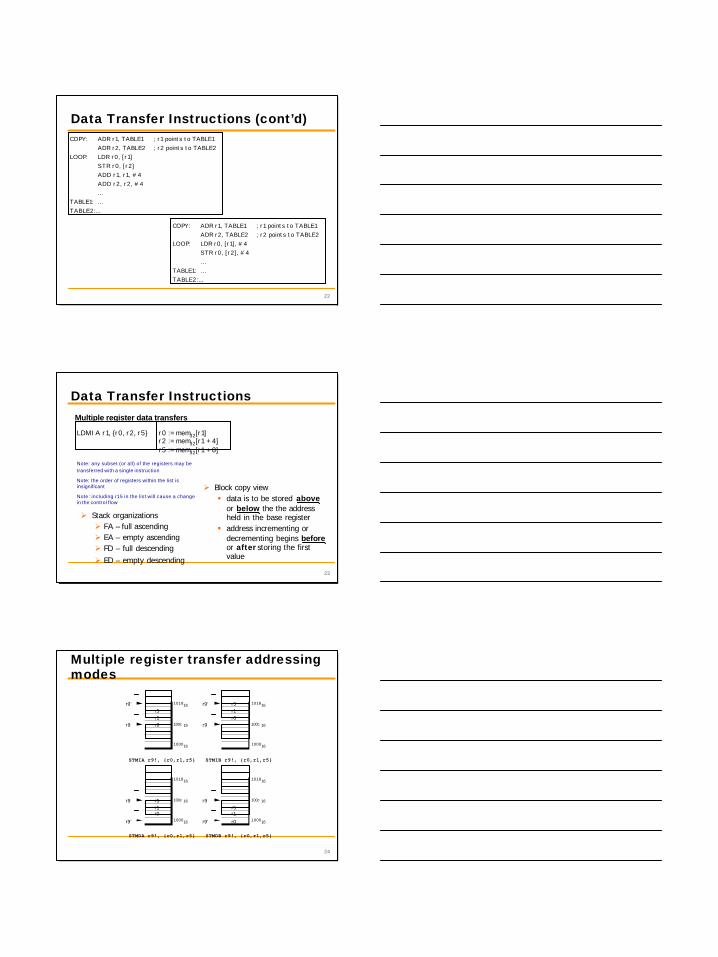
Data Transfer Instructions
Ø Block copy view§ data is to be stored above
or below the the address held in the base register
§ address incrementing or decrementing begins beforeor after storing the first value
r0 := mem32[r1]r2 := mem32[r1 + 4]r5 := mem32[r1 + 8]
LDMIA r1, {r0, r2, r5}
Note: any subset (or all) of the registers may be transferred with a single instruction
Note: the order of registers within the list is insignificant
Note: including r15 in the list will cause a change in the control flow
Multiple register data transfers
Ø Stack organizationsØ FA – full ascending Ø EA – empty ascendingØ FD – full descendingØ ED – empty descending
24
Multiple register transfer addressing modes
r5r1
r9’
r0r9
STMIA r9!, {r0,r1,r5}
100016
100c 16
101816
r1r5r9
STMDA r9!, {r0,r1,r5}
r0
r9’ 100016
100c 16
101816
r5r9
STMDB r9!, {r0,r1,r5}
r1
r0r9’ 100016
100c 16
101816
r5r1r0
r9’
r9
STMIB r9!, {r0,r1,r5}
100016
100c 16
101816

25
The mapping between the stack and block copy views
As ce ndi ng Des ce ndi ngFul l Em pt y Ful l Em pt y
Increm entB ef o re STMIB
STMFALDMIBLDMED
Aft er STMIASTMEA
LDMIALDMFD
Dec re me ntB ef o re LDMDB
LDMEASTMDBSTMFD
Aft er LDMDALDMFA
STMDASTMED
26
Control flow instructionsBranch Interpretation Normal uses B BAL
Unconditional Always
Always take this branch Always take this branch
BEQ Equa l Comparison equal or zero result BNE Not equal Comparison not equal or non-zero result BPL Plus Result positive or zero BMI Minus R e sult minus or negative BCC B L O
Carry clear L o w e r
Arithmetic operation did not give carry-out Unsigned comparison gave lower
BCS BHS
Carry set Higher or same
Arithmetic operation gave carry-out Unsigned comparison gave higher or same
BVC Overflow clear Signed integer operation; no overflow occurred BVS Overflow set Signed integer operation; overflow occurred B G T Greater than Signed integer comparison gave greater than BGE Greater or equal Signed integer comparison gave greater or
equal B L T Less than S igned integer comparison gave less than B L E Less or equal Signed integer comparison gave less than or
equal BHI Higher Unsigned comparison gave higher B L S Lower or same Unsigned comparison gave lower or same
27
Conditional executionØ Conditional execution to avoid branch instructions used to
skip a small number of non-branch instructionsØ Example
CMP r0, #5 ; BEQ BYPASS ; if (r0!=5) {ADD r1, r1, r0 ; r1:=r1+r0-r2SUB r1, r1, r2 ; }
BYPASS: .. .
CMP r0, #5 ; ADDNE r1, r1, r0 ; SUBNE r1, r1, r2 ; . . .
With conditional execution
Note: add 2 –letter condition after the 3 -letter opcode
; if ((a==b) && (c==d)) e++;
CMP r0, r1CMPEQ r2, r3ADDEQ r4, r4, #1
28
Branch and link instructionsØ Branch to subroutine (r14 serves as a link register)
Ø Nested subroutines
BL SUBR ; branch to SUBR.. ; return here
SUBR: .. ; SUBR entry pointMOV pc, r14 ; return
BL SUB1..
SUB1: ; save work and link registerSTMFD r13!, {r0-r2,r14} BL SUB2..LDMFD r13!, {r0-r2,pc}
SUB2: ..MOV pc, r14 ; copy r14 into r15
29
Supervisor callsØ Supervisor is a program which operates at a privileged
level – it can do things that a user-level program cannot do directly§ Example: send text to the display
Ø ARM ISA includes SWI (SoftWare Interrupt)
; output r0[7:0]
SWI SWI_ WriteC; return from a user program back to monitorSWI SWI_Exit
30
Jump tablesØ Call one of a set of subroutines depending on a value
computed by the programBL JTAB...
JTAB: CMP r0, #0BEQ SUB0CMP r0, #1BEQ SUB1CMP r0, #2BEQ SUB2
Note: slow when the list is long, and all subroutines are equally frequent
BL JTAB...
JTAB: ADR r1, SUBTABCMP r0, #SUBMAX ; overrun?LDRLS pc, [r1, r0, LSL #2]B ERROR
SUBTAB: DCD SUB0DCD SUB1DCD SUB2...
31
Hello ARM World!AREA HelloW, CODE, READONLY ; declare code area
SWI_ WriteC EQU &0 ; output character in r0SWI_Exit EQU &11 ; finish program
ENTRY ; code entry pointSTART: ADR r1, TEXT ; r1 <- Hello ARM World!LOOP: LDRB r0, [r1], #1 ; get the next byte
CMP r0, #0 ; check for text endSWINE SWI_ WriteC ; if not end of string, print BNE LOOPSWI SWI_Exit ; end of execution
TEXT = “Hello ARM World!”, &0a, &0d, 0END
ARMOrganization and Implementation
Aleksandar MilenkovicE-mail: [email protected]: http://www. ece.uah.edu/~milenka
33
OutlineØ ARM ArchitectureØ ARM Organization and Implementation
Ø ARM Instruction SetØ Architectural Support for High-level Languages
Ø Thumb Instruction SetØ Architectural Support for System Development
Ø ARM Processor CoresØ Memory Hierarchy
Ø Architectural Support for Operating SystemsØ ARM CPU Cores
Ø Embedded ARM Applications

34
ARM organizationØ Register file –§ 2 read ports, 1 write port +
1 read, 1 write port reserved for r15 (pc)
Ø Barrel shifter – shift or rotate one operand for any number of bits
Ø ALU – performs the arithmetic and logic functions required
Ø Memory address register + incrementer
Ø Memory data registersØ Instruction decoder and
associated control logic
multiply
data out register
instructiondecode
&
control
incrementer
registerbank
address register
barrelshifter
A[31:0]
D[31:0]
data in register
ALU
control
PC
PC
ALU
bus
A
bus
B
bus
register
35
Three-stage pipelineØ Fetch§ the instruction is fetched from memory and placed in the
instruction pipeline
Ø Decode§ the instruction is decoded and the datapath control signals
prepared for the next cycle; in this stage the instruction owns the decode logic but not the datapath
Ø Execute§ the instruction owns the datapath; the register bank is read,
an operand shifted, the ALU register generated and written back into a destination register
36
ARM single-cycle instruction pipeline
fetch decode execute
time
1
fetch decode execute
fetch decode execute
2
3instruction

37
ARM single-cycle instruction pipeline
add r0,r1,#5
sub r2,r3,r6
cmp r2,#3
fetch
time
decode
fetch
execute add
decode
fetch
execute sub
decode execute cmp
1 2 3
38
ARM multi-cycle instruction pipeline
fetch ADD decode execute
t ime
1
fetch STR decode calc. addr.
fetch ADD decode execute
2
3
data xfer
fetch ADD decode execute4
5 fetch ADD decode execute
instruction
Decode logic is always generating the control signals for the datapath to use in the next cycle
39
ARM multi-cycle LDMIA (load multiple) instruction
fetch decodeex ld r2ldmiar0,{r2,r3}
sub r2,r3,r6
cmp r2,#3
ex ld r3
fetch
time
decode ex sub
fetch decodeex cmp
Decode stage occupied since ldmia must continue toremember decoded instruction
sub fetched at normal time butnot decoded until LDMIA is finishing
Instruction delayed

40
Control stalls: due to branchesØ Branches often introduce stalls (branch penalty)§ Stall time may depend on whether branch is taken
Ø May have to squash instructions that already started executing
Ø Don’t know what to fetch until condition is evaluated
41
ARM pipelined branch
time
fetch decode ex bnebne foo
subr2,r3,r6
fetch decode
foo addr0,r1,r2
ex bne
fetch decode ex add
ex bne
Decision not made until the third clock cycle
Two cycles of work thrown away if bne takes place
42
Pipeline: how it worksØ All instructions occupy the datapath
for one or more adjacent cyclesØ For each cycle that an instruction occupies the datapath,
it occupies the decode logic in the immediately preceding cycle
Ø During the fist datapath cycle each instruction issues a fetch for the next instruction but one
Ø Branch instruction flush and refill the instruction pipeline

43
ARM9TDMI 5-stage pipeline
I-cache
rot/sgn ex
+4
byte repl.
ALU
I decode
register read
D-cache
fetch
instructiondecode
execute
buffer/data
write-back
forwardingpaths
immediatefields
nextpc
regshift
load/storeaddress
LDR pc
SUBS pc
post-index
pre-index
LDM/STM
register write
r15
pc+8
pc + 4
+4
mux
shift
mul
B, BLMOV pc
Ø Fetch Ø DecodeØ instruction is decodedØ register operands read
(3 read ports)Ø Execute Ø an operand is shifted and
the ALU result generated, orØ address is computed
Ø Buffer/dataØ data memory is accessed
(load, store)Ø Write-back Øwrite to register file
44
ARM9TDMI Data Forwarding
I-cache
rot/sgn ex
+4
byte repl.
ALU
I decode
register read
D-cache
fetch
instructiondecode
execute
buffer/data
write-back
forwardingpaths
immediatefields
nextpc
regshift
load/storeaddress
LDR pc
SUBS pc
post-index
pre-index
LDM/STM
register write
r15
pc+8
pc + 4
+4
mux
shift
mul
B, BLMOV pc
r3 := r2 + 8 x r1r5 := r5 + 2r2 x r3
ADD r3, r2, r1, LSL #3ADD r5, r5, r3, LSL r2
r3 := r2 + 8 x r1r8 := r9 + r10r5 := r5 + 2r2 x r3
ADD r3, r2, r1, LSL #3ADD r8, r9, r10ADD r5, r5, r3, LSL r2
r3 := mem[r2]r1 := r2 + r3
LD r3, [r2] ADD r1, r2, r3
Data Forwarding
Stall?
45
ARM9TDMI PC generation
I-cache
rot/sgn ex
+4
byte repl.
ALU
I decode
register read
D-cache
fetch
instructiondecode
execute
buffer/data
write-back
forwardingpaths
immediatefields
nextpc
regshift
load/storeaddress
LDR pc
SUBS pc
post-index
pre-index
LDM/STM
register write
r15
pc+8
pc + 4
+4
mux
shift
mul
B, BLMOV pc
Ø 3-stage pipelineØ PC behavior:
operands are read in execution stage r15 = PC + 8
Ø 5-stage pipelineØ operands are read in decode
stage and r15 = PC + 4?Ø incompatibilities between 3-
stage and 5-stage implementations => unacceptable
Ø to avoid this 5-stage pipeline ARMs emulate the behavior of the older 3-stage designs

46
Data processing instruction datapath activity (Ex)
address register
increment
registersRd
Rn
PC
Rm
as ins.
as instruction
mult
data out data in i. pipe
(a) register – register operations
address register
increment
registersRd
Rn
PC
as ins.
as instruction
mult
data out data in i. pipe
[7:0]
(b) register – immediate operations
ØReg-RegØRd = Rn op RmØr15 = AR + 4
AR = AR + 4ØReg-ImmØRd = Rn op ImmØr15 = AR + 4
AR = AR + 4
47
STR (store register) datapath activity(Ex1, Ex2)
address register
increment
registersRn
PC
lsl#0
= A / A+ B / A - B
mult
data out data in i. pipe
[11:0]
address register
increment
registersRn
Rd
shifter
= A+ B / A - B
mult
PC
byte? data in i. pipe
(a) 1s t cycle – compute address (b) 2nd cycle – store data & auto-index
ØCompute address (Ex1)ØAR = Rn op DispØr15 = AR + 4
ØStore data (Ex2)ØAR = PCØmem[AR] =
Rd<x:y>ØIf autoindexing
=>Rn = Rn +/- 4
48
The first two (of three) cycles of a branch instruction
address register
increment
registersPC
lsl#2
= A + B
mult
data out data in i. pipe
[23:0]
address register
increment
registersR14
PC
shifter
= A
mult
data out data in i. pipe
(a) 1s t cycle – compute branch target (b) 2nd cycle – save return address
Third cycle: do a small correction to the value stored in the link register in order that it points to directly at the instruction which follows the branch?
ØCompute target addressØAR = PC + Disp,lsl #2
ØSave return address (if required)Ør14 = PCØAR = AR + 4

49
ARM ImplementationØ Datapath§ RTL (Register Transfer Level)
Ø Control unit§ FSM (Finite State Machine)
50
2-phase non-overlapping clock schemeØ Most ARMs do not operate on edge-sensitive registersØ Instead the design is based around
2-phase non-overlapping clocks which are generated internally from a single clock signal
Ø Data movement is controlled by passing the data alternatively through latches which are open during phase 1 or latches during phase 2
1 clock cycle
phase 1
phase 2
51
ARM datapath timingØ Register read§ Register read buses – dynamic, precharged during phase 2§ During phase 1 selected registers discharge the read buses
which become valid early in phase 1Ø Shift operation§ second operand passes through barrel shifter
Ø ALU operation§ ALU has input latches which are open in phase 1,
allowing the operands to begin combining in ALU as soon as they are valid, but they close at the end of phase 1 so that the phase 2 precharge does not get through to the ALU
§ ALU processes the operands during the phase 2, producing the valid output towards the end of the phase
§ the result is latched in the destination register at the end of phase 2

52
ARM datapath timing (cont’d)
read bus valid
shift out valid
ALU out
shift time
ALU time
registerwrite time
registerreadtime
ALU operandslatched
phase 1
ph ase 2
prechargeinvalidatesbuses
Minimum Datapath Delay = Register read time + Shifter Delay + ALU Delay+ Register write set-up time + Phase 2 to phase 1 non-overlap time
53
The original ARM1 ripple-carry adderØ Carry logic: use CMOS AOI (And-O r-Invert) gateØ Even bits use circuit show below
Ø Odd bits use the dual circuit with inverted inputs and outputs and AND and OR gates swapped around
Ø Worst case path:32 gates long
AB
Cin
sum
Cout
54
ARM2 4-bit carry look-ahead schemeØ Carry Generate (G)
Carry Propagate (P)Ø Cout[3] =Cin[0].P + G
Ø Use AOI and alternate AND/OR gates
Ø Worst case:8 gates long
A[3:0]
B[3:0]
Cin[0]
sum[3:0]
Cout[3]
4-bitadderlogic
P
G

55
The ARM2 ALU logic for one result bitØ ALU functions§ data operations (add, sub, ...)§ address computations for memory accesses§ branch target computations§ bit-wise logical
operations§ ...
ALUbus
432105
NBbus
NAbus
carrylogic
fs:
G
P
56
ARM2 ALU function codes
fs 5 f s4 f s 3 f s2 f s1 f s 0 ALU o ut put0 0 0 1 0 0 A an d B0 0 1 0 0 0 A an d not B0 0 1 0 0 1 A x or B0 1 1 0 0 1 A p lus no t B p lus carry0 1 0 1 1 0 A p lus B p lus carry1 1 0 1 1 0 no t A plus B p lus carry0 0 0 0 0 0 A0 0 0 0 0 1 A o r B0 0 0 1 0 1 B0 0 1 0 1 0 no t B0 0 1 1 0 0 zer o
57
The ARM6 carry-select adder schemeØ Compute sums of
various fields of the wordfor carry -in of zero and carry -in of one
Ø Final result is selected by using the correct carry -in value to control a multiplexor
sum[31:16]sum[15:8]sum[7:4]sum[3:0]
s s+1
a,b[31:28]a,b[3:0]
+ +, +1c
+, +1
mux
mux
mux
Worst case: O(log2[word width]) gates long
Note: Be careful! Fan-out on some of these gates is high so direct comparison with previous schemes is not applicable.
58
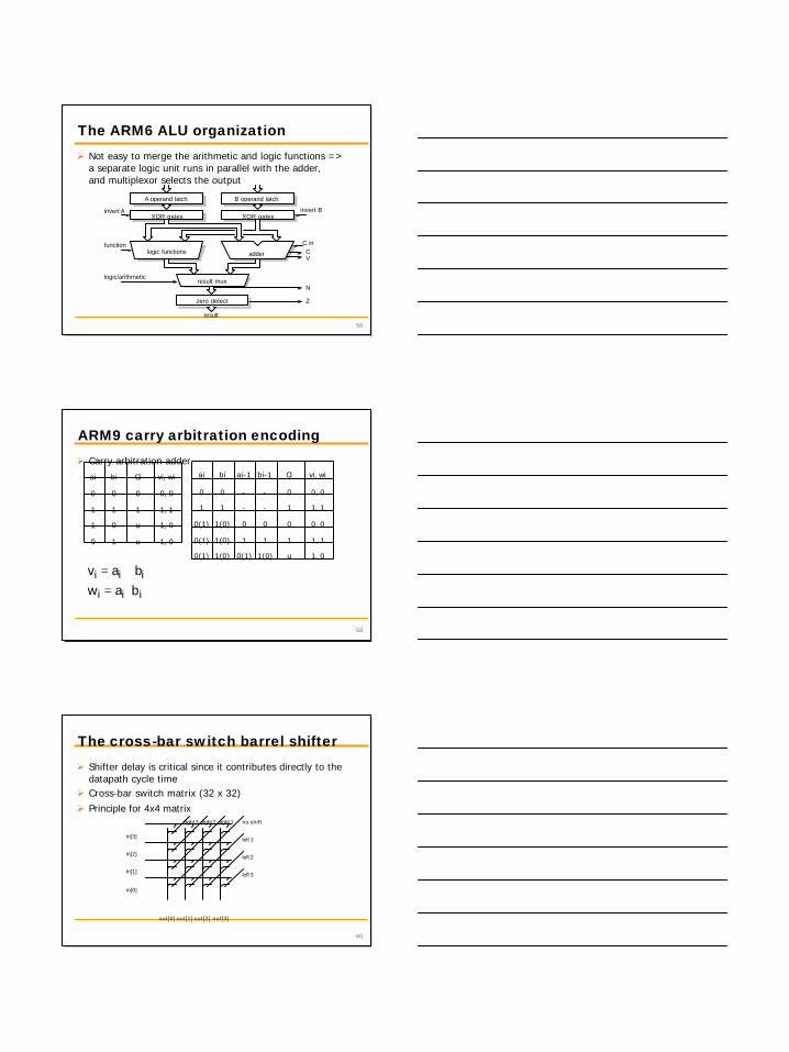
The ARM6 ALU organizationØ Not easy to merge the arithmetic and logic functions =>
a separate logic unit runs in parallel with the adder, and multiplexor selects the output
Z
N
VC
logic/arithmetic
C infunction
invert A invert B
result
result mux
logic functions
A operand latch B operand latch
XOR gates XOR gates
adder
zero detect
59
ARM9 carry arbitration encodingØ Carry arbitration adder
u
u
1
0
Ci
1, 010
1, 001
1, 111
0, 000
ai vi, wibi
u
1
0
1
0
Ci
1, 01(0)0(1)1(0)0(1)
1(0)
1(0)
1
0
bi
0(1)
0(1)
1
0
ai
1, 111
0, 000
1, 1--
0, 0--
vi, wibi-1ai-1
iii
iiibawbav
⋅=+=
60
The cross-bar switch barrel shifterØ Shifter delay is critical since it contributes directly to the
datapath cycle timeØ Cross-bar switch matrix (32 x 32)
Ø Principle for 4x4 matrix
in[0]
in[1]
in[2]
in[3]
out[0] out[1] out[2] out[3]
no shiftright 1right 2right 3
left 1
left 2
left 3

61
The cross-bar switch barrel shifter (cont’d)Ø Precharged logic is used =>
each switch is a single NMOS transistorØ Precharging sets all outputs to logic 0, so those which are
not connected to any input during switching remain at 0 giving the zero filling required by the shift semantics
Ø For rotate right, the right shift diagonal is enabled + complementary shift left diagonal (e. g., ‘right 1’ + ‘left 3’)
Ø Arithmetic shift right:use sign-extension => separate logic is used to decode the shift amount and discharge those outputs appropriately
62
Multiplier designØ All ARMs apart form the first prototype have included
support for integer multiplication§ older ARM cores include low-cost multiplication hardware
that supports only the 32-bit result multiply and multiply -accumulate§ recent ARM cores have high-performance multiplication
hardware and support 64-bit result multiply andmultiply -accumulate
Ø Low cost implementation§ Use the datapath iteratively, employing the barrel shifter
and ALU to generate 2-bit product in each clock cycle§ use early termination to stop the iterations when there are
no more ones in the multiply register
63
The 2-bit multiplication algorithm, Nth cycleØ Control settings for the Nth cycle of the multiplicationØ Use existing shifter and ALU + additional hardware§ dedicated two-bits-per-cycle shift register for the multiplier
and a few gates for the Booth’s algorithm control logic(overhead is a few per cent on the area of ARM core)
Carry - in Mult i pli e r Shi ft AL U Ca rry - o ut0 x 0 LSL # 2N A + 0 0
x 1 LSL # 2N A + B 0x 2 LSL # (2N + 1 ) A – B 1x 3 LSL # 2N A – B 1
1 x 0 LSL # 2N A + B 0x 1 LSL # (2N + 1 ) A + B 0x 2 LSL # 2N A – B 1x 3 LSL # 2N A + 0 1

64
High speed multiplicationØ Where multiplication performance is very important,
more hardware resources must be dedicated § in some embedded systems the ARM core is used to perform
real-time digital signal processing (DSP) –DSP programs are typically multiplication intensive
Ø Use intermediate results which include partial sums and partial carries § Carry -save adders are used for this
Ø These two binary results are added together at the end of multiplication§ The main ALU is used for this
65
Carry-propagate (a) and carry-save (b) adder structuresØ Carry propagate adder takes two conventional (irredundant) binary
numbers as inputs and produces a binary sum Ø Carry save adder takes one binary and one redundant (partial sum and
partial carry) input and produces a sum in redundant binary representation (sum and carry)
+A B Cin
Cout S(a) +
A B Cin
Cout S+
A B Cin
Cout S+
A B Cin
Cout S
+A B Cin
Cout S(b) +
A B Cin
Cout S+
A B Cin
Cout S+
A B Cin
Cout S
66
ARM high-speed multiplier organizationØ CSA has 4 layers of adders each handling 2 multiplier bits
=> multiply 8-bits per clock cycleØ Partial sum and carry are cleared at the beginning
or initialized to accumulate a valueØ Multiplier is shifted right 8-bits
per cycle in the ‘Rs’ registerØ Carry sum and carry
are rotated right 8 bits per cycleØ Performance: up to 4 clock cycles
(early termination is possible)Ø Complexity: 160 bits in shift registers,
128 bits of carry -save adder logic (up to 10% of simpler cores)

67
ARM high-speed multiplier organization
Rs >> 8 bits/cycle
carry-save adders
partial sum
partial carry
initiali zation for MLA registers
Rm
ALU (add partials)
rotate sum andcarry 8 bits/cycle
68
ARM2 register cell circuit
A busB bus
ALU bus
writeread
Bread
A
69
ARM register bank floorplan
A bus read decoders
B bus read decoders
write decoders
register cellsPC
Vdd
Vss
ALUbus
PCbus
INCbus
ALUbus
A bus
B bus

70
ARM core datapath buses
address register
incrementer
register bank
multiplier
ALU
shifter
data in
instruction pipe
data out
A B
W
instruction
Din
shift out
PC
Ad
inc
71
ARM control logic structure
decodePLA
cyclecount
multiplycontrol
load/storemultiple
addresscontrol
registercontrol
ALUcontrol
shiftercontrol
instruction
coprocessor