Arial bold 34ptGene-6320 - EMAC Inc. | Single Board ... Express Module NanoCOM-U15 A2.0 NanoCOM-U15...
50
COM Express Module NanoCOM-U15 A2.0 NanoCOM-U15 A2.0 Intel ® Atom TM Z530/Z510 Processor 24-bit Single Channel LVDS Onboard DDRII 533 Memory High Definition Audio Onboard Solid State Disk 1 SATA II, 8 USB2.0 NanoCOM-U15 Manual Rev.A 2.0 1st Ed. March 2010
Transcript of Arial bold 34ptGene-6320 - EMAC Inc. | Single Board ... Express Module NanoCOM-U15 A2.0 NanoCOM-U15...

COM Express Module N a n o C O M - U 1 5 A 2 . 0
NanoCOM-U15 A2.0
Intel® AtomTM Z530/Z510 Processor
24-bit Single Channel LVDS
Onboard DDRII 533 Memory
High Definition Audio
Onboard Solid State Disk
1 SATA II, 8 USB2.0
NanoCOM-U15 Manual Rev.A 2.0 1st Ed. March 2010

COM Express Module N a n o C O M - U 1 5 A 2 . 0
i
Copyright Notice This document is copyrighted, 2010. All rights are reserved. The original manufacturer reserves the right to make improvements to the products described in this manual at any time without notice.
No part of this manual may be reproduced, copied, translated, or transmitted in any form or by any means without the prior written permission of the original manufacturer. Information provided in this manual is intended to be accurate and reliable. However, the original manufacturer assumes no responsibility for its use, or for any in-fringements upon the rights of third parties that may result from its use.
The material in this document is for product information only and is subject to change without notice. While reasonable efforts have been made in the preparation of this document to assure its accuracy, the manufacturer assumes no liabilities resulting from errors or omissions in this document, or from the use of the information contained herein.
The manufacturer reserves the right to make changes in the product design without notice to its users.

COM Express Module N a n o C O M - U 1 5 A 2 . 0
ii
Acknowledgments All other products’ name or trademarks are properties of their respective owners.
Award is a trademark of Award Software International, Inc.
CompactFlash™ is a trademark of the Compact Flash Association.
Intel®, Atom™ are trademarks of Intel® Corporation.
Microsoft Windows® is a registered trademark of Microsoft Corp.
ITE is a trademark of Integrated Technology Express, Inc.
IBM, PC/AT, PS/2, and VGA are trademarks of International Business Machines Corporation.
SoundBlaster is a trademark of Creative Labs, Inc.
All other product names or trademarks are properties of their respective owners.

COM Express Module N a n o C O M - U 1 5 A 2 . 0
iii
Packing List Before you begin installing your card, please make sure that the following materials have been shipped:
• 1 NanoCOM-U15 A2.0 CPU module
• 1 CD-ROM for manual (in PDF format) and drivers
• 4 M2.5 screws
If any of these items should be missing or damaged, please contact your distributor or sales representative immediately.

COM Express Module N a n o C O M - U 1 5 A 2 . 0
iv
Application Notes 1. Wake-On-LAN and PXE function For saving the battery power, the standby power in the ECB-951D (COM Express carrier board) has been removed. Therefore, the NanoCOM-U15 cannot support Wake-On-LAN and PXE function when the ECB-951D has been using. If you need the function of Wake-On-LAN or PXE, custom BIOS canbe provided. 2. USB Client Port The NanoCOM-U15 supports 8 USB ports. Port 7 can be the host or client port. It can be chosen via BIOS. 3. Legacy and legacy-free BIOS The NanoCOM-U15 equips with legacy-free BIOS in default. If you test the functions on ECB-951D accompanied with the NanoCOM-U15, please use the legacy BIOS instead of legacy-free BIOS. 4. Display Support If you want to get the display(s) not only from LVDS LCD, but also from DVI monitor for debugging, please purchase the ECB-951D. It is a COM Express carrier board and equips with SDVO to DVI daughter board to provide the DVI connector. 5. Touch Screen Controller with USB Interface If you implement a touch screen controller with USB interface in the carrier board and use Windows CE, please use USB#0, 1 and 3 of NanoCOM-U15. There is a driver support issue of Windows CE. 6. DVI display issue in Windows OS If you only connect DVI panel, it will display normally when installing OS. After installing the graphic driver, you will need to reboot the system. After booting, the display may disappear. It is Intel's driver issue. The display may change to LVDS panel even you do not connect LVDS panel and choose "DVI only" item in BIOS. You can use the below hot key to change the display from LVDS panel to DVI

COM Express Module N a n o C O M - U 1 5 A 2 . 0
v
panel: Ctrl+Alt+F4 7. DVI display issue in DOS If you connect DVI panel and LVDS panel both, only DVI panel shows the display in DOS even you choose "LVDS+DVI" item in BIOS. Display signals that come from SDVO will be the "first" and "only" display in DOS. 8. Installation of Fedora 10 (1) If you want to install Fedora 10 into on-board SSD, it may be an issue. Standard Fedora 10 can not be installed into the 4GB SSD because its capacity is not enough. (2) When installing Fedora 10, on-board SSD and SATA storage device can not exist at the same time. You need to buy the versions without onboard SSD or with higher capacity of SSD.

COM Express Module N a n o C O M - U 1 5 A 2 . 0
vi
Contents Chapter 1 General Information
1.1 Introduction................................................................ 1-2
1.2 Features .................................................................... 1-3
1.3 Specifications ............................................................ 1-4
Chapter 2 Quick Installation Guide
2.1 Safety Precautions .................................................... 2-2
2.2 Location of Connectors/Jumpers & Mechanical Drawings
......................................................................................... 2-3
2.3 List of Jumpers/ Connectors/ Switches..................... 2-4
2.4 CPLD Writing Programming Connector (JP1) .......... 2-4
2.5 AT/ATX and SSD Writing Protection Function Setting
Switch (S1) ...................................................................... 2-4
2.6 SCI & SMI Connector (CN2) ..................................... 2-5
2.7 SDVO Connector (CN3)............................................ 2-5
2.8 COM Express Row A/B Connector (CN4)................. 2-6
2.9 Storage Support Matrix ............................................. 2-11
Chapter 3 Award BIOS Setup
3.1 System Test and Initialization. .................................. 3-2
3.2 Award BIOS Setup .................................................... 3-3
Chapter 4 Driver Installation
4.1 Installation ................................................................. 4-3

COM Express Module N a n o C O M - U 1 5 A 2 . 0
vii
Appendix A Programming The Watchdog Timer
A.1 Programming .........................................................A-2
Appendix B I/O Information
B.1 I/O Address Map....................................................B-2
B.2 Memory Address Map............................................B-3
B.3 IRQ Mapping Chart ................................................B-4
B.4 DMA Channel Assignments...................................B-4

COM Express Module N a n o C O M - U 1 5 A 2 . 0
Chapter 1 General Information 1- 1
Chapter
General
1Information

COM Express Module N a n o C O M - U 1 5 A 2 . 0
Chapter 1 General Information 1- 2
1.1 Introduction
The
NanoCOM-U15 A2.0, and its accompanying carrier
board-ECB-951D, adopts Intel® AtomTM Z530/Z510 processor
and Intel® System Controller Hub US15W chipset, offering high
speed PCI-Express bus interface and serial ATA for your high
performance applications requiring high-speed and greater
stability. The COM Express CPU module offers flexibility and
time-to-market advantages over a fully customized platform.
NanoCOM-U15 A2.0 supports up to 24-bit single
channel LVDS interface and supports onboard DDRII 533
memory chip up to 1GB. A high definition audio interface is
available to connect to an audio codec on the carrier board.
Moreover, one onboard PATA SSD (Master device) and one
SATAII interfaces are featured giving the user flexibility in
storage choices.
To satisfy the requirements of leading-edge applications in
gaming, entertainment, industrial automation, medical, and POS,
etc, COM Express carrier boards can be designed with features
and technologies specifically targeting the needs of the different
market segments.
COM Express Module N a n o C O M - U 1 5 A 2 . 0
Chapter 1 General Information 1-3
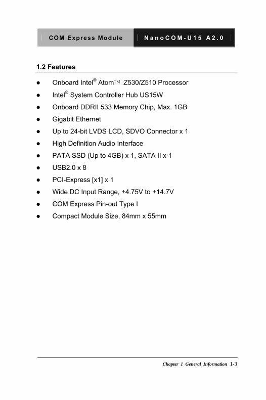
1.2 Features
Onboard Intel® Atom� Z530/Z510 Processor
Intel® System Controller Hub US15W
Onboard DDRII 533 Memory Chip, Max. 1GB
Gigabit Ethernet
Up to 24-bit LVDS LCD, SDVO Connector x 1
High Definition Audio Interface
PATA SSD (Up to 4GB) x 1, SATA II x 1
USB2.0 x 8
PCI-Express [x1] x 1
Wide DC Input Range, +4.75V to +14.7V
COM Express Pin-out Type I
Compact Module Size, 84mm x 55mm

COM Express Module N a n o C O M - U 1 5 A 2 . 0
Chapter 1 General Information 1- 4
1.3 Specifications
System
Processor Intel ® Atom� Z530/Z510
Processor
Z530: 1.6GHz/ FSB 533MHz
Z510: 1.1GHz/ FSB 400MHz
System Memory Non-ECC Onboard DDRII 533
memory chip, Max. 1GB
Chipset Intel ® System Controller Hub
US15W
I/O Chipset Intel ® System Controller Hub
US15W
Ethernet Intel ® 82574L for
10/100/1000Base-TX Ethernet x 1
BIOS Award BIOS v8.0, TSOP type,
1MB ROM
H/W status monitoring CPU Temperature Monitoring
Watchdog Timer Fintek F75111
Expansion Interface 4-bit SDIO: Multiplexed with GPIO
pins
PCI-Express﹝x1﹞x 1
LPC bus x 1
SMBus x 1
BBS Yes

COM Express Module N a n o C O M - U 1 5 A 2 . 0
Chapter 1 General Information 1-5
Power Requirement Wide DC Input Range,
+4.75V to +14.7V
2-pin wafer for RTC battery
Board Size 3.31” (L) x 2.17” (W)
(84mm x 55mm)
Gross Weight 0.44 lb (0.2kg)
Operating Temperature 32oF~140oF (0oC~60oC)
Storage Temperature -40oF~176oF (-40oC~80oC)
Operating Humidity 0%~90% relative humidity,
non-condensing
OS Support Windows 32-bit XP Pro, Windows
XP Embedded, WinCE 6.0,
Linux-Fedora 10
Display: Supports LCD/DVI or LCD/LCD (via SDVO)
Simultaneous/ Dual View Displays
Chipset Intel ® System Controller Hub
US15W integrated
Memory Shared system memory up to
256MB
Resolution Up to 1366 x 768 @ 85Hz (Max.
pixel clock of 112MHz) for LVDS;
Up to 1280 x 1024 @ 85Hz (Max.
pixel clock of 160MHz) for
SDVO

COM Express Module N a n o C O M - U 1 5 A 2 . 0
Chapter 1 General Information 1- 6
LCD Interface Up to 24-bit single channel
LVDS
SDVO SDVO connector x 1
I/O
Storage 1. PATA SSD onboard (Master
device), Max. 4GB (Optional)
2. SATA II x 1
USB USB2.0 x 8
Audio High Definition Audio
Parallel Port From LPC interface on the carrier
board
Serial Port From LPC interface on the carrier
board
GPIO Up to 4 in or 4 out: Multiplexed
with 4-bit SDIO

COM Express Module N a n o C O M - U 1 5 A 2 . 0
Chapter 2 Quick Installation Guide 2-1
Quick Installation
Chapter
2Guide
Notice:
The Quick Installation Guide is derived from Chapter 2 of user manual. For other chapters and further installation instructions, please refer to the user manual CD-ROM that came with the product.

COM Express Module N a n o C O M - U 1 5 A 2 . 0
Chapter 2 Quick Installation Guide 2 - 2
2.1 Safety Precautions
Always completely disconnect the power cord from your board whenever you are working on it. Do not make connections while the power is on, because a sudden rush of power can damage sensitive electronic components. Always ground yourself to remove any static charge before touching the board. Modern electronic devices are very sensitive to static electric charges. Use a grounding wrist strap at all times. Place all electronic components on a static-dissipative surface or in a static-shielded bag when they are not in the chassis

COM Express Module N a n o C O M - U 1 5 A 2 . 0
Chapter 2 Quick Installation Guide 2 - 3
2.2 Location of Connectors/ Jumpers & Mechanical Drawings
Component Side
Solder Side

COM Express Module N a n o C O M - U 1 5 A 2 . 0
Chapter 2 Quick Installation Guide 2 - 4
2.3 List of Jumpers/ Connectors/ Switches
The board has a number of jumpers, connectors and switches that allow you to configure your system to suit your application.
The table below shows the function of them:
Label Function
JP1 CPLD Writing Programming Connector
S1 AT/ATX and SSD Writing Protection Function Setting Switch
CN2 SCI & SMI Connector
CN3 SDVO Connector
CN4 COM Express Connector
2.4 CPLD Writing Programming Connector (JP1)
Pin Signal Pin Signal 1 TMS 2 TDI
3 TDO 4 TCK
5 GND 6 +3.3V_DUAL
2.5 AT/ATX and SSD Writing Protection Function Setting
Switch (S1)
ON
1 2
ON
1 2
ON
1 2
ON
1 2AT SSD-D AT
SSD-E ATXSSD-D
ATX SSD-E
Label Function
1 (On) ATX (Default)

COM Express Module N a n o C O M - U 1 5 A 2 . 0
Chapter 2 Quick Installation Guide 2 - 5
1 (Off) AT
2 (On) SSD Writing Protection Function Enable (SSD-E)
2 (Off) SSD Writing Protection Function Disable (SSD-D) (Default)
2.6 SCI & SMI Connector (CN2)
Pin Signal
1 EC_SCI
2 SMI#
2.7 SDVO Connector (CN3)
Pin Signal Pin Signal
1 GND 2 SDVO_CLK#
3 SDVO_CLK 4 GND 5 SDVO_GREEN# 6 SDVO_GREEN 7 GND 8 SDVO_INT# 9 SDVO_INT 10 GND
11 SDVO_BLUE# 12 SDVO_BLUE 13 GND 14 SDVO_RED# 15 SDVO_RED 16 GND 17 SDVO_STALL# 18 SDVO_STALL 19 GND 20 SDVO_CTRLCLK_R 21 SDVO_CTRLDATA_R 22 SDVO_RST#
23 +3.3V 24 +2.5V 25 +5V 26 GND 27 TVCLKIN# 28 TVCLKIN 29 +3.3V 30 +5V

COM Express Module N a n o C O M - U 1 5 A 2 . 0
Chapter 2 Quick Installation Guide 2 - 6
2.8 COM Express Row A/B Connector (CN4)
Row A Row B
A1 GND (FIXED) B1 GND (FIXED)
A2 GBE0_MDI3- B2 GBE0_ACT#
A3 GBE0_MDI3+ B3 LPC_FRAME#
A4 GBE0_LINK100# B4 LPC_AD0
A5 GBE0_LINK1000# B5 LPC_AD1
A6 GBE0_MDI2- B6 LPC_AD2
A7 GBE0_MDI2+ B7 LPC_AD3
A8 GBE0_LINK# B8 LPC_DRQ0#
A9 GBE0_MDI1- B9 N.C.
A10 GBE0_MDI1+ B10 LPC_CLK
A11 GND (FIXED) B11 GND (FIXED)
A12 GBE0_MDI0- B12 PWRBTN#
A13 GBE0_MDI0+ B13 SMB_CK
A14 GBE0_CTREF B14 SMB_DAT
A15 SUS_S3# B15 SMB_ALERT#
A16 SATA0_TX+ B16 N.C.
A17 SATA0_TX- B17 N.C.
A18 SUS_S5# B18 N.C.
A19 SATA0_RX+ B19 N.C.
A20 SATA0_RX- B20 N.C.
A21 GND (FIXED) B21 GND (FIXED)

COM Express Module N a n o C O M - U 1 5 A 2 . 0
Chapter 2 Quick Installation Guide 2 - 7
A22 N.C. B22 N.C.
A23 N.C. B23 N.C.
A24 SUS_S5# B24 PWR_OK
A25 N.C. B25 N.C.
A26 N.C. B26 N.C.
A27 N.C. B27 WDT
A28 IDELED# B28 N.C.
A29 AC_SYNC B29 AC_SDIN1
A30 AC_RST# B30 AC_SDIN0
A31 GND (FIXED) B31 GND (FIXED)
A32 AC_BITCLK B32 SPKR
A33 AC_SDOUT B33 I2C_CK
A34 BIOS_DISABLE# B34 I2C_DAT
A35 THRMTRIP# B35 THRM#
A36 USB3- B36 USB2-
A37 USB3+ B37 USB2+
A38 USB_6_7_OC# B38 USB_4_5_OC#
A39 USB6- B39 USB7-
A40 USB6+ B40 USB7+
A41 GND (FIXED) B41 GND (FIXED)
A42 USB4- B42 USB5-
A43 USB4+ B43 USB5+
A44 USB_2_3_OC# B44 USB_0_1_OC#
A45 USB0- B45 USB1-

COM Express Module N a n o C O M - U 1 5 A 2 . 0
Chapter 2 Quick Installation Guide 2 - 8
A46 USB0+ B46 USB1+
A47 VCC_RTC B47 N.C.
A48 EXCD0_PERST# B48 N.C.
A49 N.C. B49 SYS_RESET#
A50 LPC_SERIRQ B50 CB_RESET#
A51 GND (FIXED) B51 GND (FIXED)
A52 N.C. B52 N.C.
A53 N.C. B53 N.C.
A54 GPI0 D54 B54 GPO1
A55 N.C. B55 N.C.
A56 N.C. B56 N.C.
A57 GND B57 GPO2
A58 N.C. B58 N.C.
A59 N.C. B59 N.C.
A60 GND (FIXED) B60 GND (FIXED)
A61 N.C. B61 N.C.
A62 N.C. B62 N.C.
A63 GPI1 B63 GPO3
A64 N.C. B64 N.C.
A65 N.C. B65 N.C.
A66 GND B66 WAKE0#
A67 GPI2 B67 WAKE1#
A68 PCIE_TX0+ B68 PCIE_RX0+
A69 PCIE_TX0- B69 PCIE_RX0-

COM Express Module N a n o C O M - U 1 5 A 2 . 0
Chapter 2 Quick Installation Guide 2 - 9
A70 GND (FIXED) B70 GND (FIXED)
A71 LVDS_A0+ B71 N.C.
A72 LVDS_A0- B72 N.C.
A73 LVDS_A1+ B73 N.C.
A74 LVDS_A1- B74 N.C.
A75 LVDS_A2+ B75 N.C.
A76 LVDS_A2- B76 N.C.
A77 LVDS_VDD_EN B77 N.C.
A78 LVDS_A3+ B78 N.C.
A79 LVDS_A3- B79 LVDS_BKLT_EN
A80 GND (FIXED) B80 GND (FIXED)
A81 LVDS_A_CK+ B81 N.C.
A82 LVDS_A_CK- B82 N.C.
A83 LVDS_I2C_CK B83 LVDS_BKLT_CTRL
A84 LVDS_I2C_DAT B84 VCC_5V_SBY
A85 GPI3 B85 VCC_5V_SBY
A86 KBD_RST# B86 VCC_5V_SBY
A87 N.C. B87 VCC_5V_SBY
A88 PCIE0_CK_REF+ B88 RSVD
A89 PCIE0_CK_REF- B89 N.C.
A90 GND (FIXED) B90 GND (FIXED)
A91 RSVD (EC_SCI) B91 N.C.
A92 RSVD (SMI#) B92 N.C.
A93 GPO0 B93 N.C.

COM Express Module N a n o C O M - U 1 5 A 2 . 0
Chapter 2 Quick Installation Guide 2 - 10
A94 RSVD B94 N.C.
A95 RSVD B95 N.C.
A96 GND B96 N.C.
A97 VCC_12V B97 N.C.
A98 VCC_12V B98 N.C.
A99 VCC_12V B99 N.C.
A100 GND (FIXED) B100 GND (FIXED)
A101 VCC_12V B101 VCC_12V
A102 VCC_12V B102 VCC_12V
A103 VCC_12V B103 VCC_12V
A104 VCC_12V B104 VCC_12V
A105 VCC_12V B105 VCC_12V
A106 VCC_12V B106 VCC_12V
A107 VCC_12V B107 VCC_12V
A108 VCC_12V B108 VCC_12V
A109 VCC_12V B109 VCC_12V
A110 GND (FIXED) B110 GND (FIXED)
Note: Multi-function pins for 4-bit SDIO
COM Express Module N a n o C O M - U 1 5 A 2 . 0
Chapter 2 Quick Installation Guide 2 - 11
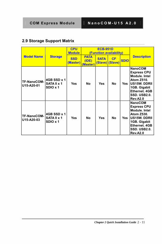
2.9 Storage Support Matrix
CPU Module
ECB-951D (Function availability)
Model Name Storage SSD (Master)
PATA (IDE)
(Master)
SATA(Slave)
CF (Slave) SDIO
Description
TF-NanoCOM-U15-A20-01
4GB SSD x 1SATA II x 1 SDIO x 1
Yes No Yes No Yes
NanoCOM Express CPU Module. Intel Atom Z510. US15W. DDRII 1GB. Gigabit Ethernet. 4GB SSD. USB2.0. Rev.A2.0
TF-NanoCOM-U15-A20-03
4GB SSD x 1SATA II x 1 SDIO x 1
Yes No Yes No Yes
NanoCOM Express CPU Module. Intel Atom Z530. US15W. DDRII 1GB. Gigabit Ethernet. 4GB SSD. USB2.0. Rev.A2.0

COM Express Module N a n o C O M - U 1 5 A 2 . 0
Chapter 2 Quick Installation Guide 2 - 12
Below Table for China RoHS Requirements 产品中有毒有害物质或元素名称及含量
Main Board/ Daughter Board/ Backplane
有毒有害物质或元素
部件名称 铅
(Pb)
汞
(Hg)
镉
(Cd)
六价铬
(Cr(VI))
多溴联苯
(PBB)
多溴二苯醚
(PBDE)
印刷电路板
及其电子组件 × ○ ○ ○ ○ ○
外部信号
连接器及线材 × ○ ○ ○ ○ ○
O:表示该有毒有害物质在该部件所有均质材料中的含量均在
SJ/T 11363-2006 标准规定的限量要求以下。 X:表示该有毒有害物质至少在该部件的某一均质材料中的含量超出
SJ/T 11363-2006 标准规定的限量要求。 备注:此产品所标示之环保使用期限,系指在一般正常使用状况下。

COM Express Module N a n o C O M - U 1 5 A 2 . 0
Chapter 3 Award BIOS Setup 3-1
Chapter
Award
3BIOS Setup

COM Express Module N a n o C O M - U 1 5 A 2 . 0
Chapter 3 Award BIOS Setup 3-2
3.1 System Test and Initialization
These routines test and initialize board hardware. If the routines encounter an error during the tests, you will either hear a few short beeps or see an error message on the screen. There are two kinds of errors: fatal and non-fatal. The system can usually continue the boot up sequence with non-fatal errors. Non-fatal error messages usually appear on the screen along with the following instructions:
Press <F1> to RESUME
Write down the message and press the F1 key to continue the boot up sequence.
System configuration verification
These routines check the current system configuration against the values stored in the CMOS memory. If they do not match, the program outputs an error message. You will then need to run the BIOS setup program to set the configuration information in memory.
There are three situations in which you will need to change the CMOS settings:
1. You are starting your system for the first time
2. You have changed the hardware attached to your system
3. The CMOS memory has lost power and the configuration information has been erased.

COM Express Module N a n o C O M - U 1 5 A 2 . 0
Chapter 3 Award BIOS Setup 3-3
3.2 Award BIOS Setup
Awards BIOS ROM has a built-in Setup program that allows users to modify the basic system configuration. This type of information is stored in battery-backed CMOS RAM so that it retains the Setup information when the power is turned off.
Entering Setup Power on the computer and press <Del> immediately. This will allow you to enter Setup.
Standard CMOS Features Use this menu for basic system configuration. (Date, time, IDE, etc.)
Advanced BIOS Features Use this menu to set the advanced features available on your system.
Advanced Chipset Features Use this menu to change the values in the chipset registers and optimize your system performance.
Integrated Peripherals Use this menu to specify your settings for integrated peripherals. (Primary slave, secondary slave, keyboard, mouse etc.)
Power Management Setup
Use this menu to specify your settings for power management. (HDD power down, power on by ring, KB wake up, etc.)
PnP/PCI Configurations
This entry appears if your system supports PnP/PCI.

COM Express Module N a n o C O M - U 1 5 A 2 . 0
Chapter 3 Award BIOS Setup 3-4
PC Health Status
This menu allows you to set the shutdown temperature for your system.
Frequency/Voltage Control
Use this menu to specify your settings for auto detect DIMM/PCI clock and spread spectrum.
Load Fail-Safe Defaults
Use this menu to load the BIOS default values for the minimal/stable performance for your system to operate.
Load Optimized Defaults Use this menu to load the BIOS default values that are factory settings for optimal performance system operations. While AWARD has designated the custom BIOS to maximize performance, the factory has the right to change these defaults to meet their needs.
Set Supervisor/User Password Use this menu to set Supervisor/User Passwords.
Save and Exit Setup Save CMOS value changes to CMOS and exit setup.
Exit Without Saving
Abandon all CMOS value changes and exit setup.

COM Express Module N a n o C O M - U 1 5 A 2 . 0
Chapter 4 Driver Installation 4 -1
Chapter
Driver
4Installation
.

COM Express Module N a n o C O M - U 1 5 A 2 . 0
Chapter 4 Driver Installation 4 -2
The NanoCOM-U15 A2.0 comes with an AutoRun CD-ROM that
contains all drivers and utilities that can help you to install the driver
automatically.
Insert the driver CD, the driver CD-title will auto start and show the
installation guide. If not, please follow the sequence below to install
the drivers.
Follow the sequence below to install the drivers: Step 1 – Install INF Driver
Step 2 – Install VGA Driver
Step 3 – Install LAN Driver
Step 4 – Install Audio Driver
Step 5 – Install Touch Panel Driver
USB 2.0 Drivers are available for download using Windows® Update for both Windows® XP and Windows® 2000. For additional information regarding USB 2.0 support in Windows® XP and Windows® 2000, please visit www.microsoft.com/hwdev/usb/.
Please read instructions below for further detailed installations.

COM Express Module N a n o C O M - U 1 5 A 2 . 0
Chapter 4 Driver Installation 4 -3
4.1 Installation:
Insert the NanoCOM-U15 A2.0 CD-ROM into the CD-ROM drive.
And install the drivers from Step 1 to Step 5 in order.
Step 1 – Install INF Driver
1. Click on the Step 1 – INF folder and double click on the
Infinst_autol.exe
2. Follow the instructions that the window shows
3. The system will help you install the driver automatically
Step 2 – Install VGA Driver
1. Click on the Step 2 – VGA folder and double click on the
Setup.exe
2. Follow the instructions that the window shows
3. The system will help you install the driver automatically
Step 3 –Install LAN Driver
1. Click on the Step 3 – LAN folder and double click on the
pro2kxp_v13_1_2.exe file
2. Follow the instructions that the window shows
3. The system will help you install the driver automatically
Step 4 –Install Audio Driver
1. Click on the Step 4 –Audio folder and double click on

COM Express Module N a n o C O M - U 1 5 A 2 . 0
Chapter 4 Driver Installation 4 -4
Setup.exe file
2. Follow the instructions that the window shows
3. The system will help you install the driver automatically
Step 5 –Install Touch Panel Driver
1. Click on the Step 5 –Touch Panel folder and double click
on the Setup.exe
2. Follow the instructions that the window shows
3. The system will help you install the driver automatically

COM Express Module N a n o C O M - U 1 5 A 2 . 0
Appendix A Programming the Watchdog Timer A-1
Programming the
Appendix
AWatchdog Timer
COM Express Module N a n o C O M - U 1 5 A 2 . 0
Appendix A Programming the Watchdog Timer A-2
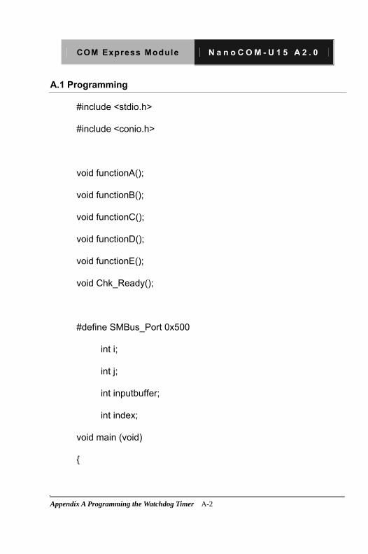
A.1 Programming
#include <stdio.h>
#include <conio.h>
void functionA();
void functionB();
void functionC();
void functionD();
void functionE();
void Chk_Ready();
#define SMBus_Port 0x500
int i;
int j;
int inputbuffer;
int index;
void main (void)
{

COM Express Module N a n o C O M - U 1 5 A 2 . 0
Appendix A Programming the Watchdog Timer A-3
char option_var='x';
//device ID(smbus):6Eh,index:03h data:03h
outportb(SMBu s_Port+0x04,0x6E);
delay(5);
outportb(SMBu s_Port+0x02,0x54);
delay(5) ;
outportb(SMBu s_Port+0x03,0x00);
delay(5) ;
outportb(SMBu s_Port+0x05,0x03);
delay(5) ;
outportb(SMBu s_Port+0x06,0x03);
delay(5) ;
outportb(SMBu s_Port+0x00,0x08);
delay(5) ;
outportb(SMBu s_Port+0x01,0x0F);
delay(5) ;
outportb(SMBu s_Port+0x00,0x12);
delay(5) ;

COM Express Module N a n o C O M - U 1 5 A 2 . 0
Appendix A Programming the Watchdog Timer A-4
Chk_Ready();
while(option_var!='0')
{
printf("0.quit\n");
printf("1. 5 sec \n");
printf("2. 10 sec \n");
printf("3. 60 sec \n");
printf("4. 256 sec \n");
printf("Please Select One option\n");
option_var = getchar();
getchar();
printf("input = %c ,pls wait\n",option_var);
switch(option_var)
{
COM Express Module N a n o C O M - U 1 5 A 2 . 0
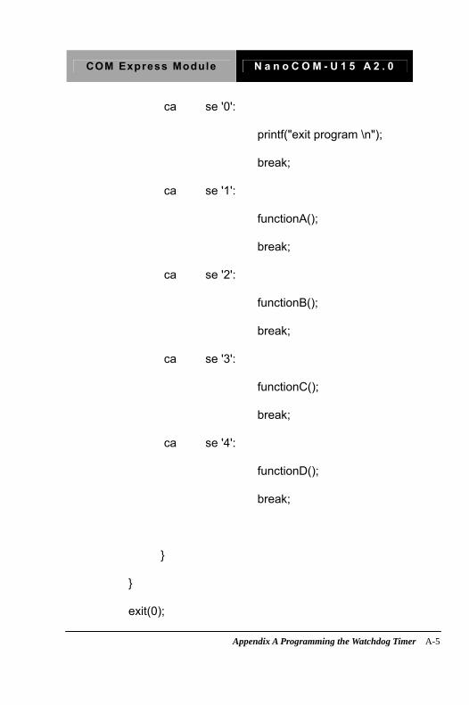
Appendix A Programming the Watchdog Timer A-5
ca se '0':
printf("exit program \n");
break;
ca se '1':
functionA();
break;
ca se '2':
functionB();
break;
ca se '3':
functionC();
break;
ca se '4':
functionD();
break;
}
}
exit(0);

COM Express Module N a n o C O M - U 1 5 A 2 . 0
Appendix A Programming the Watchdog Timer A-6
}
void functionA()
{
outportb(SMBu s_Port+0x05,0x37);
delay(5) ;
outportb(SMBu s_Port+0x06,0x05);
delay(5) ;
outportb(SMBu s_Port+0x00,0x08);
delay(5) ;
outportb(SMBu s_Port+0x01,0x0F);
delay(5) ;
outportb(SMBu s_Port+0x00,0x12);
delay(5) ;
Chk_Ready();
outportb(SMBu s_Port+0x05,0x36);
delay(5) ;
outportb(SMBu s_Port+0x06,0x73);

COM Express Module N a n o C O M - U 1 5 A 2 . 0
Appendix A Programming the Watchdog Timer A-7
delay(5) ;
outportb(SMBu s_Port+0x00,0x08);
delay(5) ;
outportb(SMBu s_Port+0x01,0x0F);
delay(5) ;
outportb(SMBu s_Port+0x00,0x12);
delay(5) ;
Chk_Ready();
}
void functionB()
{
outportb(SMBu s_Port+0x05,0x37);
delay(5) ;
outportb(SMBu s_Port+0x06,0x0A);
delay(5) ;
outportb(SMBu s_Port+0x00,0x08);
delay(5) ;

COM Express Module N a n o C O M - U 1 5 A 2 . 0
Appendix A Programming the Watchdog Timer A-8
outportb(SMBu s_Port+0x01,0x0F);
delay(5) ;
outportb(SMBu s_Port+0x00,0x12);
delay(5) ;
Chk_Ready();
outportb(SMBu s_Port+0x05,0x36);
delay(5) ;
outportb(SMBu s_Port+0x06,0x73);
delay(5) ;
outportb(SMBu s_Port+0x00,0x08);
delay(5) ;
outportb(SMBu s_Port+0x01,0x0F);
delay(5) ;
outportb(SMBu s_Port+0x00,0x12);
delay(5) ;
Chk_Ready();
}

COM Express Module N a n o C O M - U 1 5 A 2 . 0
Appendix A Programming the Watchdog Timer A-9
void functionC()
{
outportb(SMBu s_Port+0x05,0x37);
delay(5) ;
outportb(SMBu s_Port+0x06,0x3C);
delay(5) ;
outportb(SMBu s_Port+0x00,0x08);
delay(5) ;
outportb(SMBu s_Port+0x01,0x0F);
delay(5) ;
outportb(SMBu s_Port+0x00,0x12);
delay(5) ;
Chk_Ready();
outportb(SMBu s_Port+0x05,0x36);
delay(5) ;
outportb(SMBu s_Port+0x06,0x73);
delay(5) ;
outportb(SMBu s_Port+0x00,0x08);

COM Express Module N a n o C O M - U 1 5 A 2 . 0
Appendix A Programming the Watchdog Timer A-10
delay(5) ;
outportb(SMBu s_Port+0x01,0x0F);
delay(5) ;
outportb(SMBu s_Port+0x00,0x12);
delay(5) ;
Chk_Ready();
}
void functionD()
{
outportb(SMBu s_Port+0x05,0x37);
delay(5) ;
outportb(SMBu s_Port+0x06,0xFF);
delay(5) ;
outportb(SMBu s_Port+0x00,0x08);
delay(5) ;
outportb(SMBu s_Port+0x01,0x0F);
delay(5) ;
outportb(SMBu s_Port+0x00,0x12);

COM Express Module N a n o C O M - U 1 5 A 2 . 0
Appendix A Programming the Watchdog Timer A-11
delay(5) ;
Chk_Ready();
outportb(SMBu s_Port+0x05,0x36);
delay(5) ;
outportb(SMBu s_Port+0x06,0x73);
delay(5) ;
outportb(SMBu s_Port+0x00,0x08);
delay(5) ;
outportb(SMBu s_Port+0x01,0x0F);
delay(5) ;
outportb(SMBu s_Port+0x00,0x12);
delay(5) ;
Chk_Ready();
}
void Chk_Ready()
{

COM Express Module N a n o C O M - U 1 5 A 2 . 0
Appendix A Programming the Watchdog Timer A-12
index=0;
while(index<0x800)
{
inputbuffer=in portb(SMBus_Port+0x01);
delay(5);
if((inpu tbuffer&0x08)==0)
return;
index++;
}
outportb(SMBu s_Port+0x00,0x08);
delay(5);
}

COM Express Module N a n o C O M - U 1 5 A 2 . 0
Appendix B I/O Information B-1
I/O Information
Appendix
B

COM Express Module N a n o C O M - U 1 5 A 2 . 0
Appendix B I/O Information B-2
B.1 I/O Address Map
COM Express Module N a n o C O M - U 1 5 A 2 . 0
Appendix B I/O Information B-3
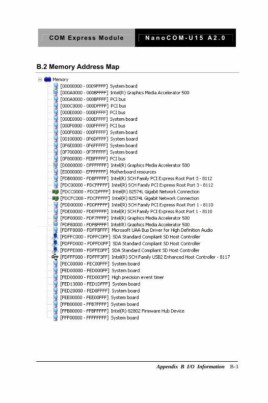
B.2 Memory Address Map

COM Express Module N a n o C O M - U 1 5 A 2 . 0
Appendix B I/O Information B-4
B.3 IRQ Mapping Chart
B.4 DMA Channel Assignments