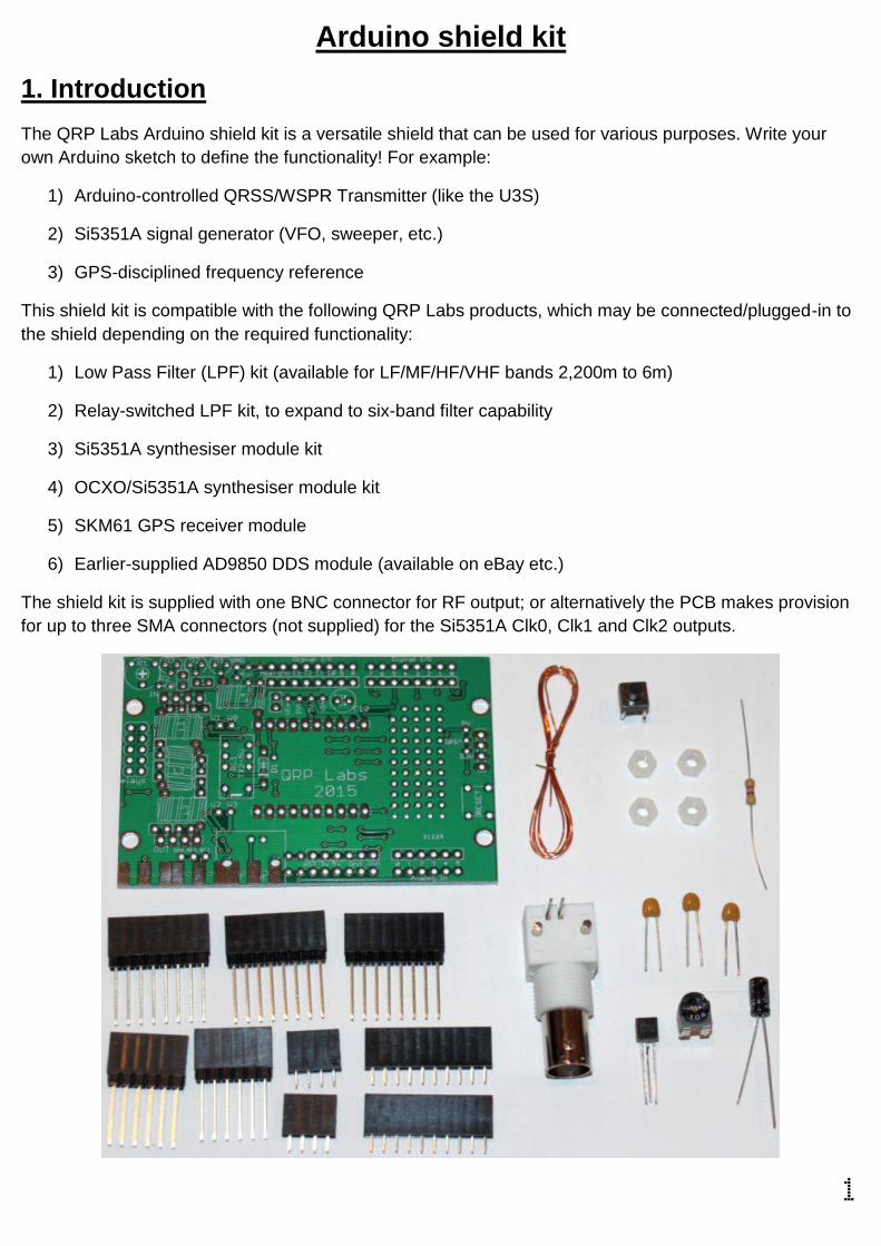
Arduino shield kit - QRP Labs · 1 Arduino shield kit 1. Introduction The QRP Labs Arduino shield...
19
1 Arduino shield kit 1. Introduction The QRP Labs Arduino shield kit is a versatile shield that can be used for various purposes. Write your own Arduino sketch to define the functionality! For example: 1) Arduino-controlled QRSS/WSPR Transmitter (like the U3S) 2) Si5351A signal generator (VFO, sweeper, etc.) 3) GPS-disciplined frequency reference This shield kit is compatible with the following QRP Labs products, which may be connected/plugged-in to the shield depending on the required functionality: 1) Low Pass Filter (LPF) kit (available for LF/MF/HF/VHF bands 2,200m to 6m) 2) Relay-switched LPF kit, to expand to six-band filter capability 3) Si5351A synthesiser module kit 4) OCXO/Si5351A synthesiser module kit 5) SKM61 GPS receiver module 6) Earlier-supplied AD9850 DDS module (available on eBay etc.) The shield kit is supplied with one BNC connector for RF output; or alternatively the PCB makes provision for up to three SMA connectors (not supplied) for the Si5351A Clk0, Clk1 and Clk2 outputs.
Transcript of Arduino shield kit - QRP Labs · 1 Arduino shield kit 1. Introduction The QRP Labs Arduino shield...
1
Arduino shield kit
1. Introduction
The QRP Labs Arduino shield kit is a versatile shield that can be used for various purposes. Write your
own Arduino sketch to define the functionality! For example:
1) Arduino-controlled QRSS/WSPR Transmitter (like the U3S)
2) Si5351A signal generator (VFO, sweeper, etc.)
3) GPS-disciplined frequency reference
This shield kit is compatible with the following QRP Labs products, which may be connected/plugged-in to
the shield depending on the required functionality:
1) Low Pass Filter (LPF) kit (available for LF/MF/HF/VHF bands 2,200m to 6m)
2) Relay-switched LPF kit, to expand to six-band filter capability
3) Si5351A synthesiser module kit
4) OCXO/Si5351A synthesiser module kit
5) SKM61 GPS receiver module
6) Earlier-supplied AD9850 DDS module (available on eBay etc.)
The shield kit is supplied with one BNC connector for RF output; or alternatively the PCB makes provision
for up to three SMA connectors (not supplied) for the Si5351A Clk0, Clk1 and Clk2 outputs.
2
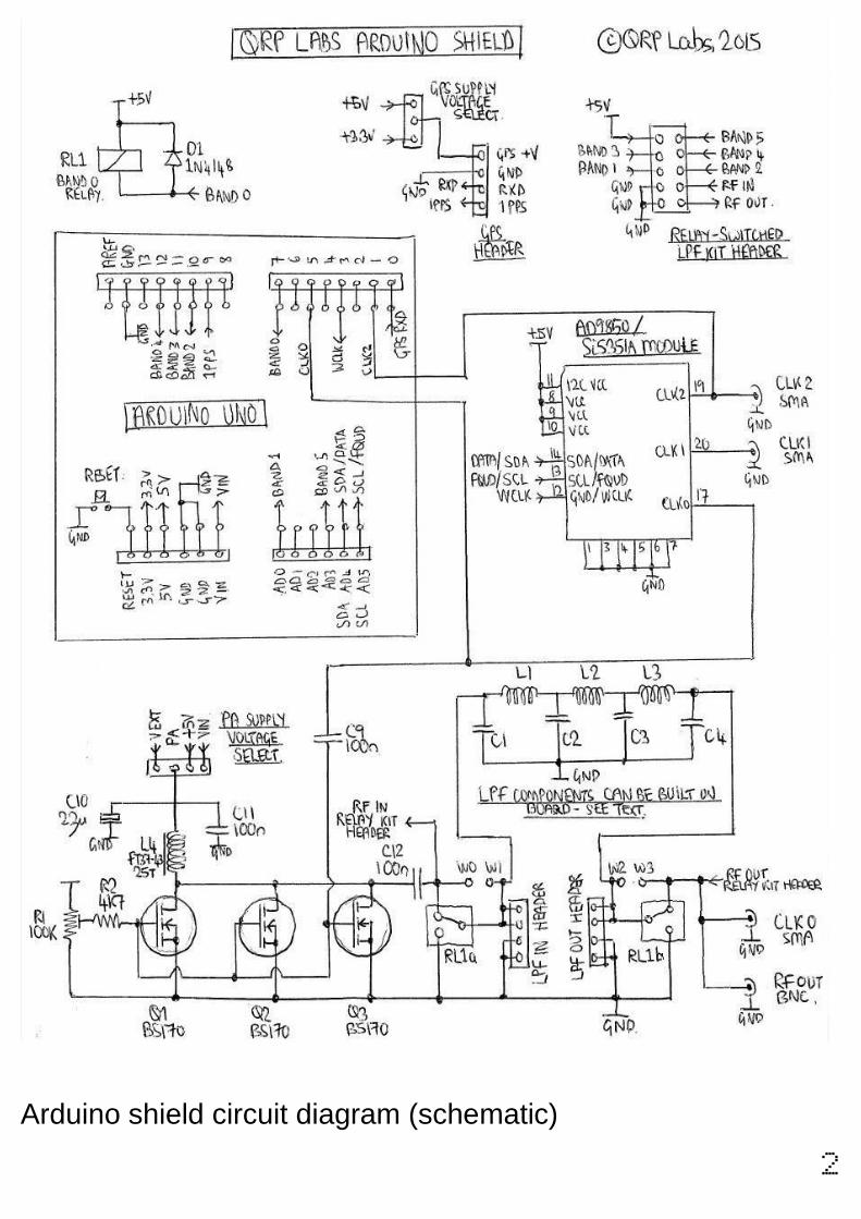
Arduino shield circuit diagram (schematic)
3
2. Parts List
2.1 Resistors
R1 100K preset potentiometer, for power amplifier bias adjustment
R2 4.7K resistor
2.2 Capacitors
C9, 10, 12 100nF (ceramic, marking 104)
C11 22uF electrolytic capacitor
C1-4 Capacitors (supplied in the Low Pass Filter kit, if fitted - see later text description)
2.3 Semiconductors
D1 1N4148 diode (supplied in the relay-switched LPF board, if fitted)
Q1 BS170 transistor
Q2, 3 BS170 transistor (not supplied – optional, for higher power output)
2.4 Miscellaneous
Push button, S1
Printed circuit board
2x 4-way female header socket
2x 10-way female header socket
2x 8-way Arduino header socket (with long pins)
3x 6-way Arduino header socket (with long pins)
4x nylon M3 nuts
50cm enamelled wire
BNC connector
FT37-43 toroidal core
3. Construction
3.1 General construction tips
Parts placement is defined by the
silkscreen printed legend on the PCB, so
please observe it carefully, paying
particular attention to the correct
orientation of the semiconductors.
It is best to read this whole manual
before you start! This is because there
are many ways to build and use this kit.
You need to understand which options to
install, for your desired use case.
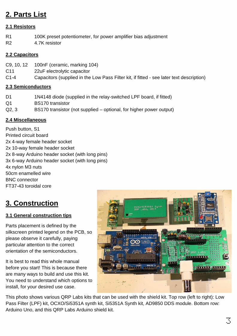
This photo shows various QRP Labs kits that can be used with the shield kit. Top row (left to right): Low
Pass Filter (LPF) kit, OCXO/Si5351A synth kit, Si5351A Synth kit, AD9850 DDS module. Bottom row:
Arduino Uno, and this QRP Labs Arduino shield kit.
4
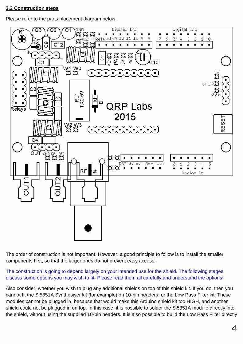
3.2 Construction steps
Please refer to the parts placement diagram below.
The order of construction is not important. However, a good principle to follow is to install the smaller
components first, so that the larger ones do not prevent easy access.
The construction is going to depend largely on your intended use for the shield. The following stages
discuss some options you may wish to fit. Please read them all carefully and understand the options!
Also consider, whether you wish to plug any additional shields on top of this shield kit. If you do, then you
cannot fit the Si5351A Synthesiser kit (for example) on 10-pin headers; or the Low Pass Filter kit. These
modules cannot be plugged in, because that would make this Arduino shield kit too HIGH, and another
shield could not be plugged in on top. In this case, it is possible to solder the Si5351A module directly into
the shield, without using the supplied 10-pin headers. It is also possible to build the Low Pass Filter directly
5
on the shield PCB, rather than plugging in low pass filter kits using the dual 4-way header system. Of
course, if you solder in the components directly on the shield, then you lose the flexibility of being able to
change them (e.g. change the LPF to a different band) just be plugging in a new LPF.
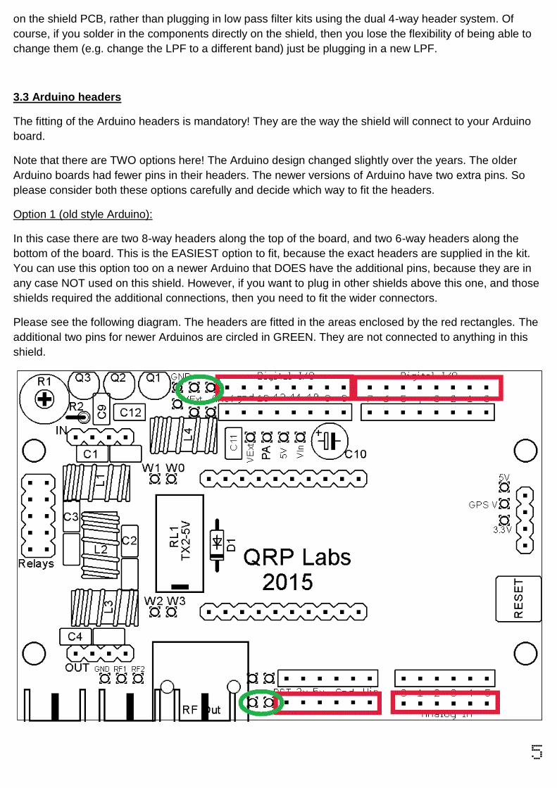
3.3 Arduino headers
The fitting of the Arduino headers is mandatory! They are the way the shield will connect to your Arduino
board.
Note that there are TWO options here! The Arduino design changed slightly over the years. The older
Arduino boards had fewer pins in their headers. The newer versions of Arduino have two extra pins. So
please consider both these options carefully and decide which way to fit the headers.
Option 1 (old style Arduino):
In this case there are two 8-way headers along the top of the board, and two 6-way headers along the
bottom of the board. This is the EASIEST option to fit, because the exact headers are supplied in the kit.
You can use this option too on a newer Arduino that DOES have the additional pins, because they are in
any case NOT used on this shield. However, if you want to plug in other shields above this one, and those
shields required the additional connections, then you need to fit the wider connectors.
Please see the following diagram. The headers are fitted in the areas enclosed by the red rectangles. The
additional two pins for newer Arduinos are circled in GREEN. They are not connected to anything in this
shield.
6
Be careful to insert the headers in the correct row of holes! Notice that there are two rows of holes along
the top, and two along the bottom of the board. The headers fit in the outermost row of holes; however the
SAFEST way to ensure you fit the headers in the correct row of holes is to CHECK with your own Arduino!
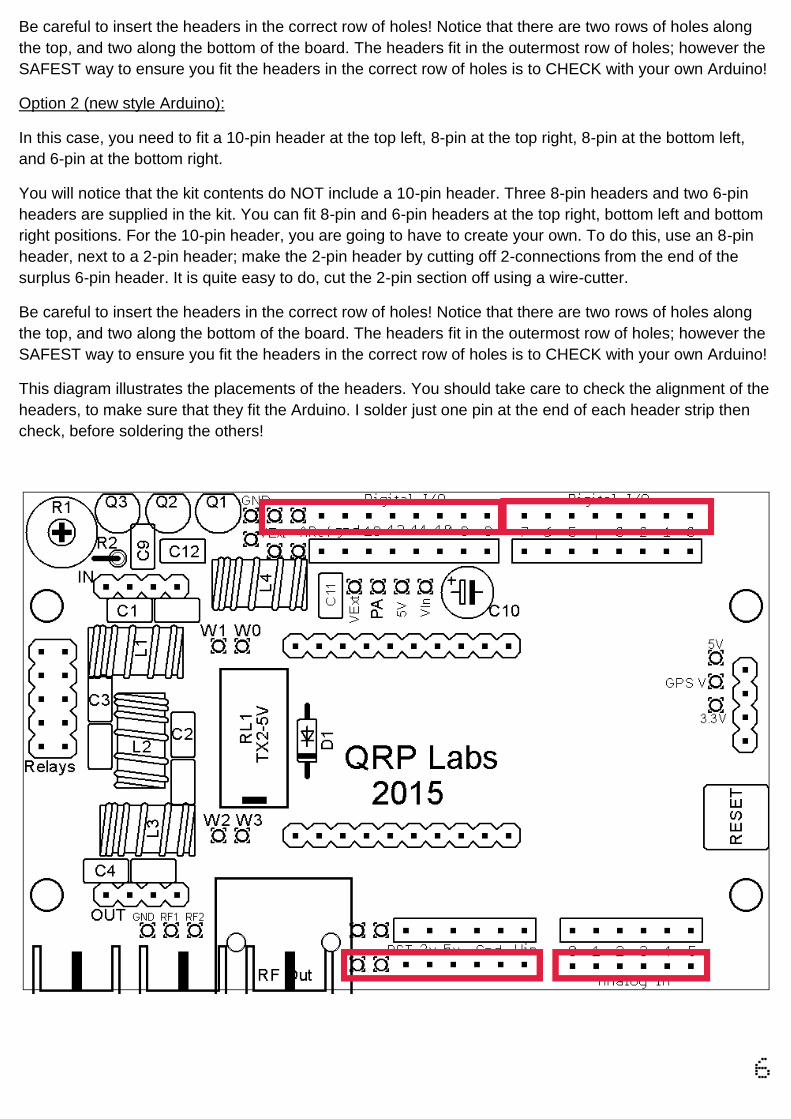
Option 2 (new style Arduino):
In this case, you need to fit a 10-pin header at the top left, 8-pin at the top right, 8-pin at the bottom left,
and 6-pin at the bottom right.
You will notice that the kit contents do NOT include a 10-pin header. Three 8-pin headers and two 6-pin
headers are supplied in the kit. You can fit 8-pin and 6-pin headers at the top right, bottom left and bottom
right positions. For the 10-pin header, you are going to have to create your own. To do this, use an 8-pin
header, next to a 2-pin header; make the 2-pin header by cutting off 2-connections from the end of the
surplus 6-pin header. It is quite easy to do, cut the 2-pin section off using a wire-cutter.
Be careful to insert the headers in the correct row of holes! Notice that there are two rows of holes along
the top, and two along the bottom of the board. The headers fit in the outermost row of holes; however the
SAFEST way to ensure you fit the headers in the correct row of holes is to CHECK with your own Arduino!
This diagram illustrates the placements of the headers. You should take care to check the alignment of the
headers, to make sure that they fit the Arduino. I solder just one pin at the end of each header strip then
check, before soldering the others!
7
This photograph shows the
PCB with the four Arduino
headers installed; this is
Option 1 (above), to suit my
Arduino Uno which is an
original Rev 1 Uno.
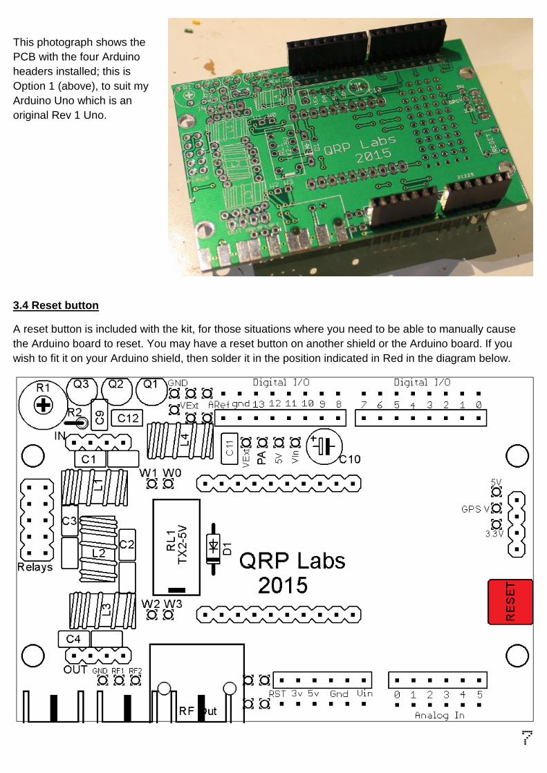
3.4 Reset button
A reset button is included with the kit, for those situations where you need to be able to manually cause
the Arduino board to reset. You may have a reset button on another shield or the Arduino board. If you
wish to fit it on your Arduino shield, then solder it in the position indicated in Red in the diagram below.
8
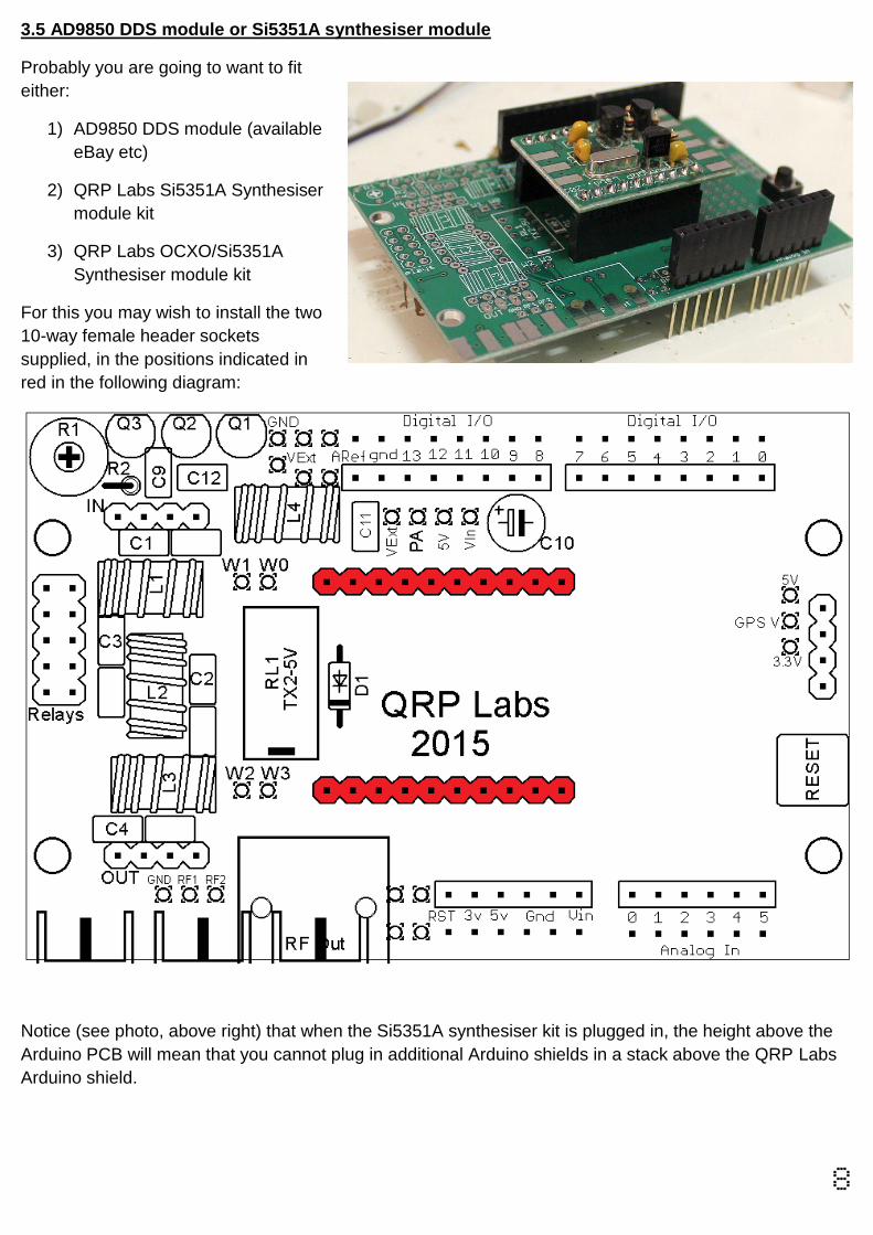
3.5 AD9850 DDS module or Si5351A synthesiser module
Probably you are going to want to fit
either:
1) AD9850 DDS module (available
eBay etc)
2) QRP Labs Si5351A Synthesiser
module kit
3) QRP Labs OCXO/Si5351A
Synthesiser module kit
For this you may wish to install the two
10-way female header sockets
supplied, in the positions indicated in
red in the following diagram:
Notice (see photo, above right) that when the Si5351A synthesiser kit is plugged in, the height above the
Arduino PCB will mean that you cannot plug in additional Arduino shields in a stack above the QRP Labs
Arduino shield.
9
Therefore another option, for people
who need to be able to plug in another
shield on top of this one, is NOT to
use the 10-way headers at all.
Instead, the AD9850 DDS module, or
Si5351A module kit, can be soldered
directly into the shield PCB. Not using
the 10-way headers will make the
overall height of the shield low
enough, to be able to plug in another
Arduino shield on top. This is shown
in this photo.
In this case, you would lose the ability
to fit the optional RL1 and D1 components (for LPF band switching), because these normally fit UNDER
the synthesiser module. Furthermore you would not be able to fit components in the prototyping area
under the synthesiser module, on the right side of the board.
You can also construct a Low Pass Filter directly on the shield PCB, rather than plugging it in using the 4-
way headers.
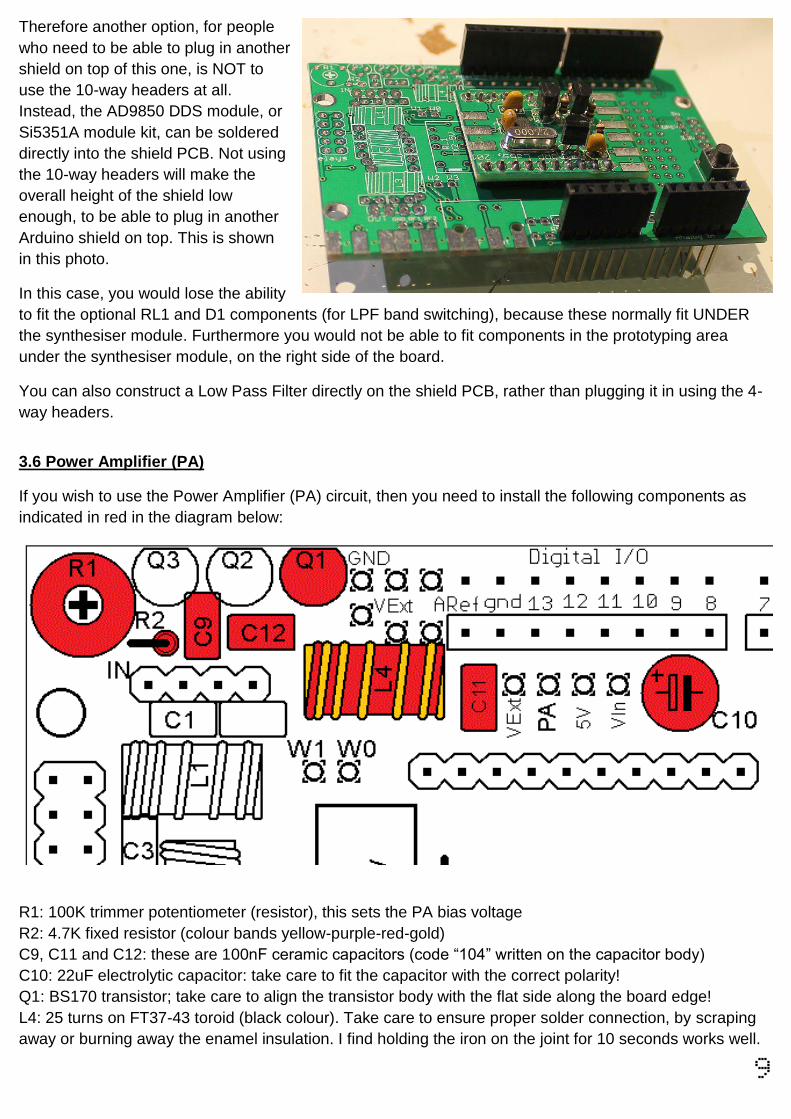
3.6 Power Amplifier (PA)
If you wish to use the Power Amplifier (PA) circuit, then you need to install the following components as
indicated in red in the diagram below:
R1: 100K trimmer potentiometer (resistor), this sets the PA bias voltage
R2: 4.7K fixed resistor (colour bands yellow-purple-red-gold)
C9, C11 and C12: these are 100nF ceramic capacitors (code “104” written on the capacitor body)
C10: 22uF electrolytic capacitor: take care to fit the capacitor with the correct polarity!
Q1: BS170 transistor; take care to align the transistor body with the flat side along the board edge!
L4: 25 turns on FT37-43 toroid (black colour). Take care to ensure proper solder connection, by scraping
away or burning away the enamel insulation. I find holding the iron on the joint for 10 seconds works well.
10
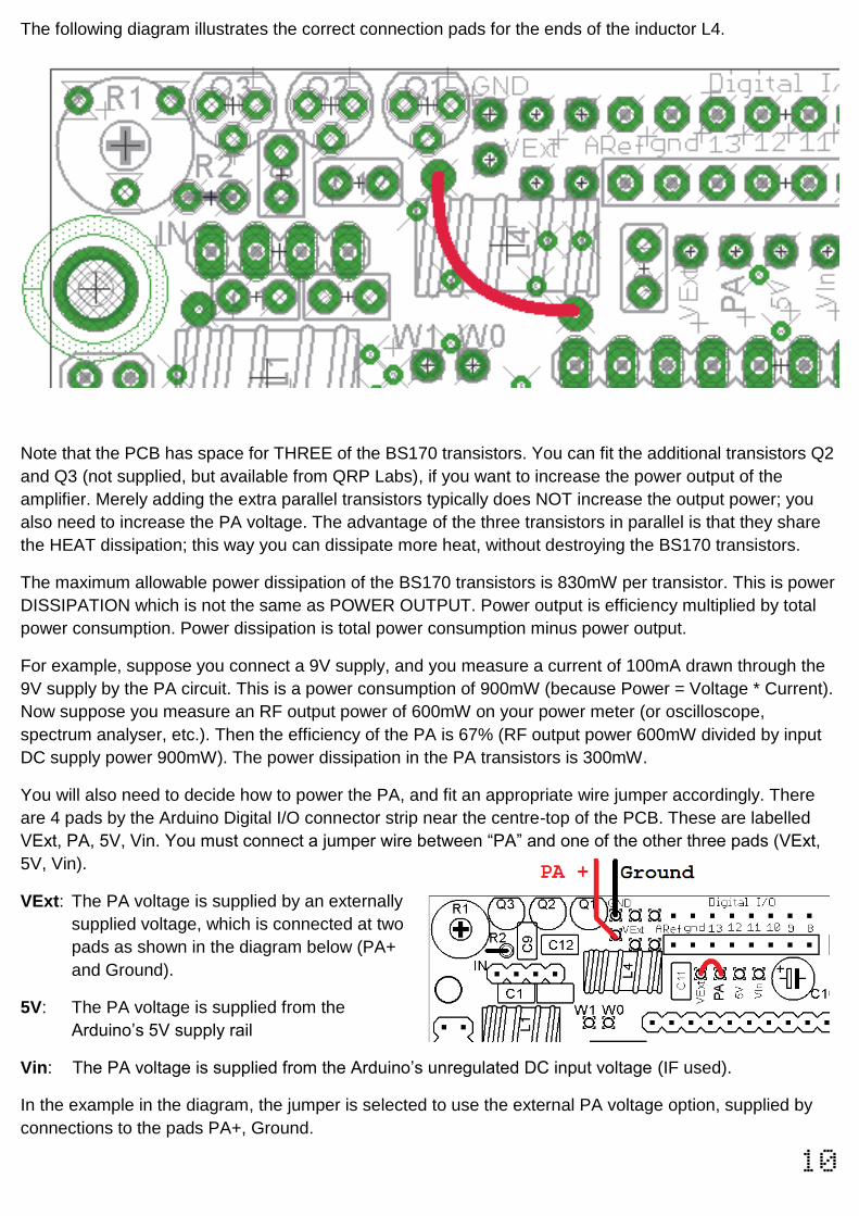
The following diagram illustrates the correct connection pads for the ends of the inductor L4.
Note that the PCB has space for THREE of the BS170 transistors. You can fit the additional transistors Q2
and Q3 (not supplied, but available from QRP Labs), if you want to increase the power output of the
amplifier. Merely adding the extra parallel transistors typically does NOT increase the output power; you
also need to increase the PA voltage. The advantage of the three transistors in parallel is that they share
the HEAT dissipation; this way you can dissipate more heat, without destroying the BS170 transistors.
The maximum allowable power dissipation of the BS170 transistors is 830mW per transistor. This is power
DISSIPATION which is not the same as POWER OUTPUT. Power output is efficiency multiplied by total
power consumption. Power dissipation is total power consumption minus power output.
For example, suppose you connect a 9V supply, and you measure a current of 100mA drawn through the
9V supply by the PA circuit. This is a power consumption of 900mW (because Power = Voltage * Current).
Now suppose you measure an RF output power of 600mW on your power meter (or oscilloscope,
spectrum analyser, etc.). Then the efficiency of the PA is 67% (RF output power 600mW divided by input
DC supply power 900mW). The power dissipation in the PA transistors is 300mW.
You will also need to decide how to power the PA, and fit an appropriate wire jumper accordingly. There
are 4 pads by the Arduino Digital I/O connector strip near the centre-top of the PCB. These are labelled
VExt, PA, 5V, Vin. You must connect a jumper wire between “PA” and one of the other three pads (VExt,
5V, Vin).
VExt: The PA voltage is supplied by an externally
supplied voltage, which is connected at two
pads as shown in the diagram below (PA+
and Ground).
5V: The PA voltage is supplied from the
Arduino’s 5V supply rail
Vin: The PA voltage is supplied from the Arduino’s unregulated DC input voltage (IF used).
In the example in the diagram, the jumper is selected to use the external PA voltage option, supplied by
connections to the pads PA+, Ground.
11
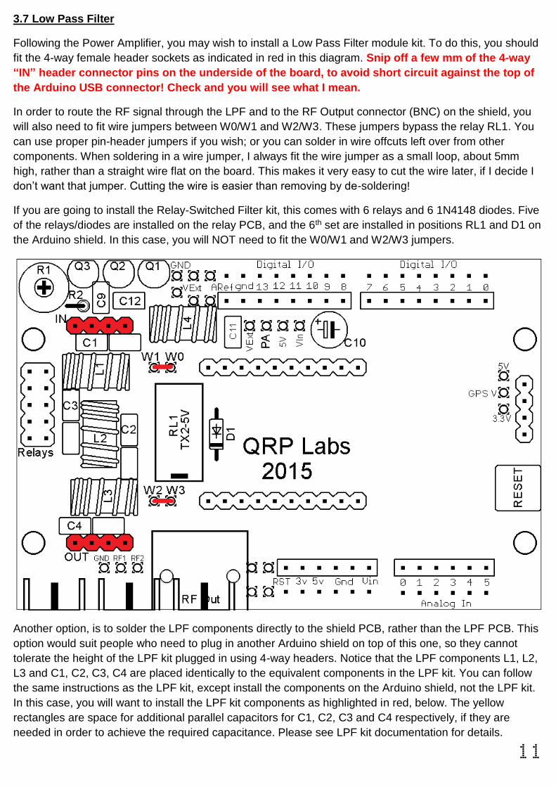
3.7 Low Pass Filter
Following the Power Amplifier, you may wish to install a Low Pass Filter module kit. To do this, you should
fit the 4-way female header sockets as indicated in red in this diagram. Snip off a few mm of the 4-way
“IN” header connector pins on the underside of the board, to avoid short circuit against the top of
the Arduino USB connector! Check and you will see what I mean.
In order to route the RF signal through the LPF and to the RF Output connector (BNC) on the shield, you
will also need to fit wire jumpers between W0/W1 and W2/W3. These jumpers bypass the relay RL1. You
can use proper pin-header jumpers if you wish; or you can solder in wire offcuts left over from other
components. When soldering in a wire jumper, I always fit the wire jumper as a small loop, about 5mm
high, rather than a straight wire flat on the board. This makes it very easy to cut the wire later, if I decide I
don’t want that jumper. Cutting the wire is easier than removing by de-soldering!
If you are going to install the Relay-Switched Filter kit, this comes with 6 relays and 6 1N4148 diodes. Five
of the relays/diodes are installed on the relay PCB, and the 6th set are installed in positions RL1 and D1 on
the Arduino shield. In this case, you will NOT need to fit the W0/W1 and W2/W3 jumpers.
Another option, is to solder the LPF components directly to the shield PCB, rather than the LPF PCB. This
option would suit people who need to plug in another Arduino shield on top of this one, so they cannot
tolerate the height of the LPF kit plugged in using 4-way headers. Notice that the LPF components L1, L2,
L3 and C1, C2, C3, C4 are placed identically to the equivalent components in the LPF kit. You can follow
the same instructions as the LPF kit, except install the components on the Arduino shield, not the LPF kit.
In this case, you will want to install the LPF kit components as highlighted in red, below. The yellow
rectangles are space for additional parallel capacitors for C1, C2, C3 and C4 respectively, if they are
needed in order to achieve the required capacitance. Please see LPF kit documentation for details.
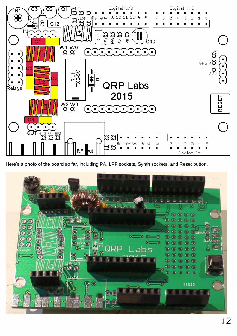
12
Here’s a photo of the board so far, including PA, LPF sockets, Synth sockets, and Reset button.
13
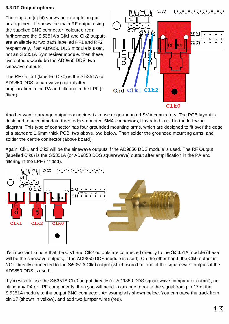
3.8 RF Output options
The diagram (right) shows an example output
arrangement. It shows the main RF output using
the supplied BNC connector (coloured red);
furthermore the Si5351A’s Clk1 and Clk2 outputs
are available at two pads labelled RF1 and RF2
respectively. If an AD9850 DDS module is used,
not an Si5351A Synthesiser module, then these
two outputs would be the AD9850 DDS’ two
sinewave outputs.
The RF Output (labelled Clk0) is the Si5351A (or
AD9850 DDS squarewave) output after
amplification in the PA and filtering in the LPF (if
fitted).
Another way to arrange output connectors is to use edge-mounted SMA connectors. The PCB layout is
designed to accommodate three edge-mounted SMA connectors, illustrated in red in the following
diagram. This type of connector has four grounded mounting arms, which are designed to fit over the edge
of a standard 1.6mm thick PCB, two above, two below. Then solder the grounded mounting arms, and
solder the centre connector (above board).
Again, Clk1 and Clk2 will be the sinewave outputs if the AD9850 DDS module is used. The RF Output
(labelled Clk0) is the Si5351A (or AD9850 DDS squarewave) output after amplification in the PA and
filtering in the LPF (if fitted).
It’s important to note that the Clk1 and Clk2 outputs are connected directly to the Si5351A module (these
will be the sinewave outputs, if the AD9850 DDS module is used). On the other hand, the Clk0 output is
NOT directly connected to the Si5351A Clk0 output (which would be one of the squarewave outputs if the
AD9850 DDS is used).
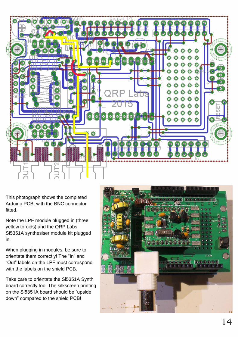
If you wish to use the Si5351A Clk0 output directly (or AD9850 DDS squarewave comparator output), not
fitting any PA or LPF components, then you will need to arrange to route the signal from pin 17 of the
Si5351A module to the output BNC connector. An example is shown below. You can trace the track from
pin 17 (shown in yellow), and add two jumper wires (red).
14
This photograph shows the completed
Arduino PCB, with the BNC connector
fitted.
Note the LPF module plugged in (three
yellow toroids) and the QRP Labs
Si5351A synthesiser module kit plugged
in.
When plugging in modules, be sure to
orientate them correctly! The “In” and
“Out” labels on the LPF must correspond
with the labels on the shield PCB.
Take care to orientate the Si5351A Synth
board correctly too! The silkscreen printing
on the Si5351A board should be “upside
down” compared to the shield PCB!
15
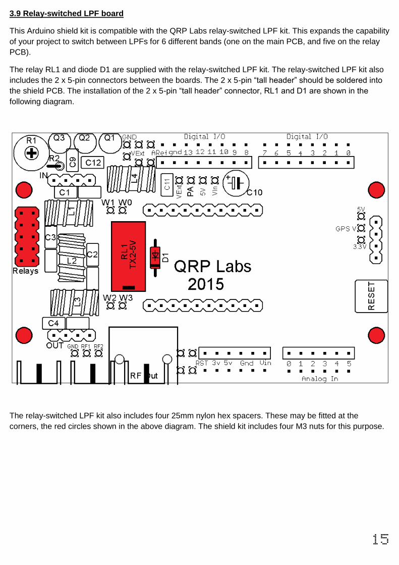
3.9 Relay-switched LPF board
This Arduino shield kit is compatible with the QRP Labs relay-switched LPF kit. This expands the capability
of your project to switch between LPFs for 6 different bands (one on the main PCB, and five on the relay
PCB).
The relay RL1 and diode D1 are supplied with the relay-switched LPF kit. The relay-switched LPF kit also
includes the 2 x 5-pin connectors between the boards. The 2 x 5-pin “tall header” should be soldered into
the shield PCB. The installation of the 2 x 5-pin “tall header” connector, RL1 and D1 are shown in the
following diagram.
The relay-switched LPF kit also includes four 25mm nylon hex spacers. These may be fitted at the
corners, the red circles shown in the above diagram. The shield kit includes four M3 nuts for this purpose.
16
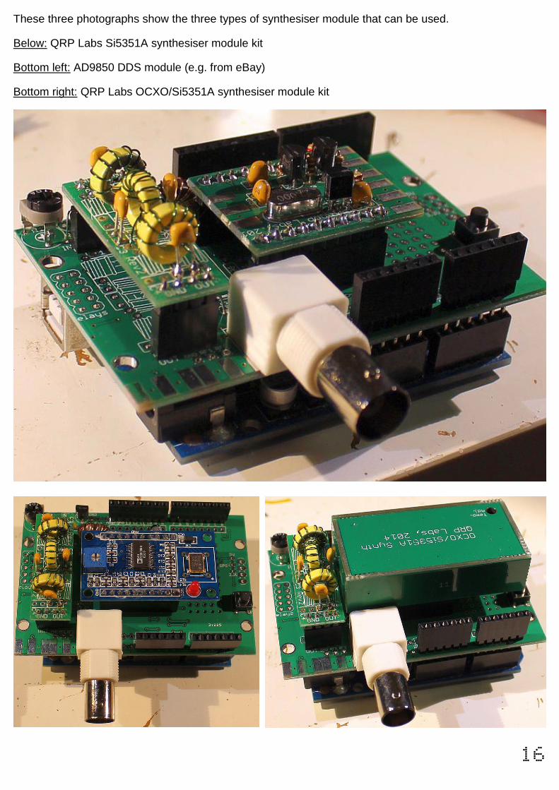
These three photographs show the three types of synthesiser module that can be used.
Below: QRP Labs Si5351A synthesiser module kit
Bottom left: AD9850 DDS module (e.g. from eBay)
Bottom right: QRP Labs OCXO/Si5351A synthesiser module kit
17
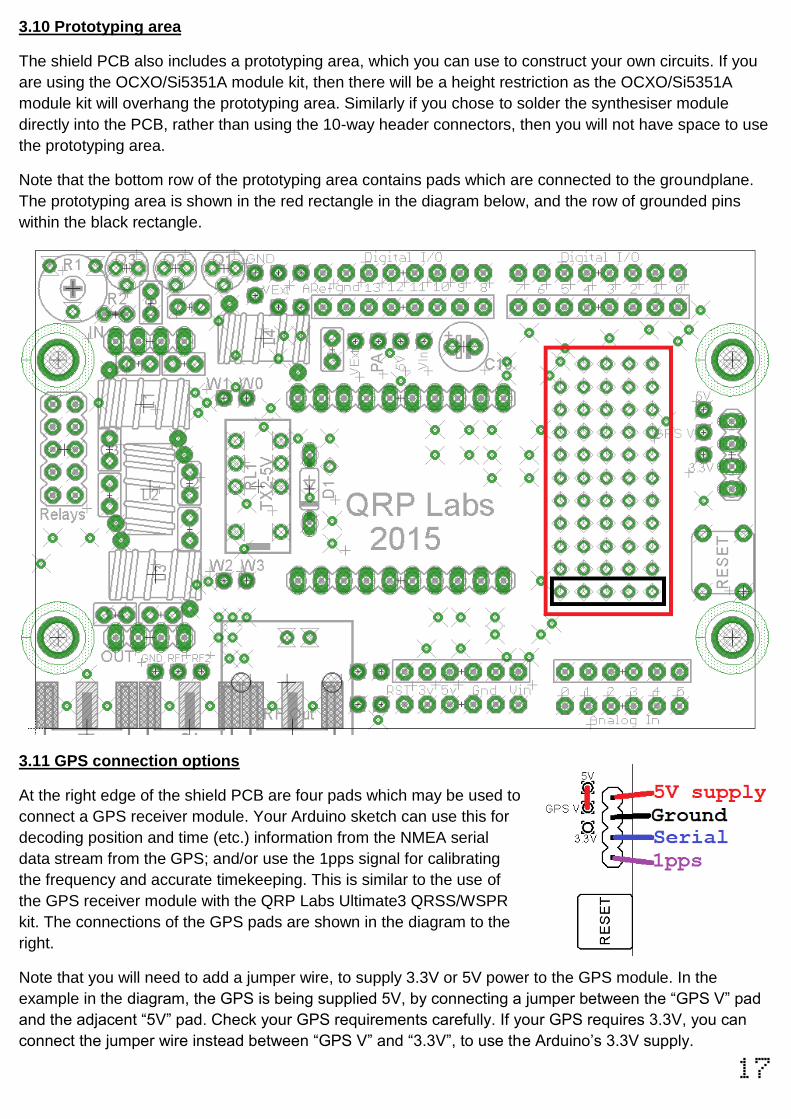
3.10 Prototyping area
The shield PCB also includes a prototyping area, which you can use to construct your own circuits. If you
are using the OCXO/Si5351A module kit, then there will be a height restriction as the OCXO/Si5351A
module kit will overhang the prototyping area. Similarly if you chose to solder the synthesiser module
directly into the PCB, rather than using the 10-way header connectors, then you will not have space to use
the prototyping area.
Note that the bottom row of the prototyping area contains pads which are connected to the groundplane.
The prototyping area is shown in the red rectangle in the diagram below, and the row of grounded pins
within the black rectangle.
3.11 GPS connection options
At the right edge of the shield PCB are four pads which may be used to
connect a GPS receiver module. Your Arduino sketch can use this for
decoding position and time (etc.) information from the NMEA serial
data stream from the GPS; and/or use the 1pps signal for calibrating
the frequency and accurate timekeeping. This is similar to the use of
the GPS receiver module with the QRP Labs Ultimate3 QRSS/WSPR
kit. The connections of the GPS pads are shown in the diagram to the
right.
Note that you will need to add a jumper wire, to supply 3.3V or 5V power to the GPS module. In the
example in the diagram, the GPS is being supplied 5V, by connecting a jumper between the “GPS V” pad
and the adjacent “5V” pad. Check your GPS requirements carefully. If your GPS requires 3.3V, you can
connect the jumper wire instead between “GPS V” and “3.3V”, to use the Arduino’s 3.3V supply.
18
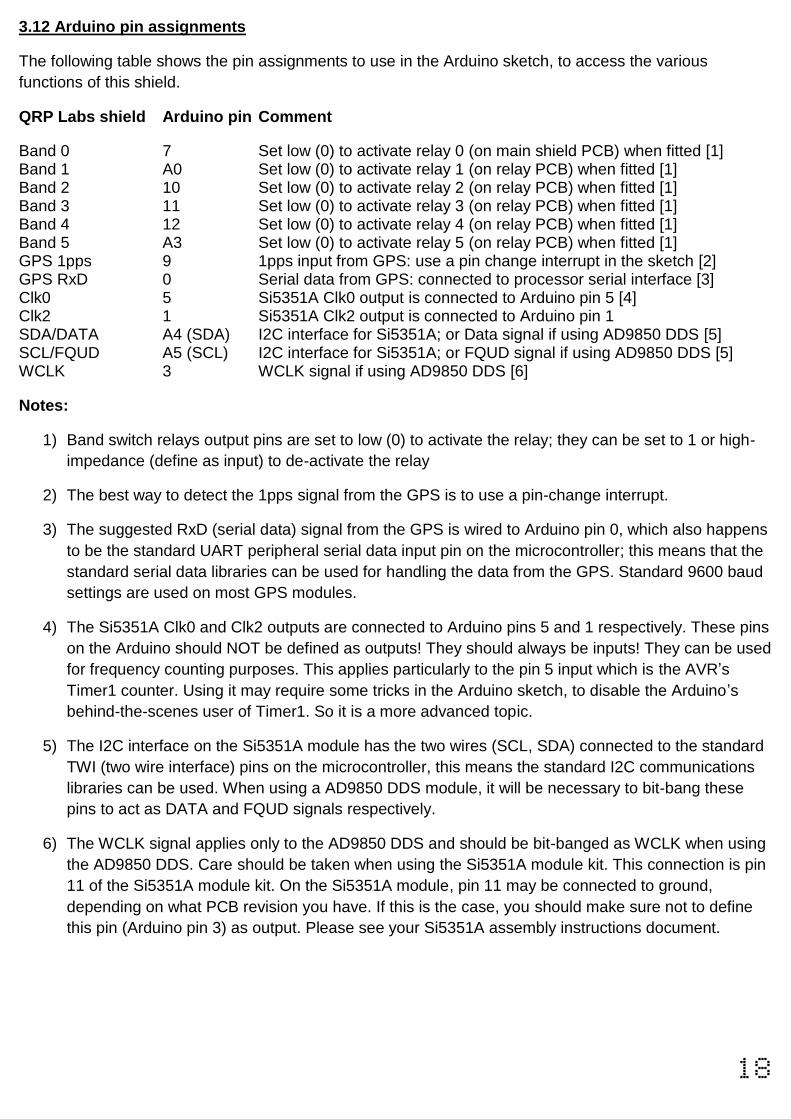
3.12 Arduino pin assignments
The following table shows the pin assignments to use in the Arduino sketch, to access the various
functions of this shield.
QRP Labs shield Arduino pin Comment
Band 0 7 Set low (0) to activate relay 0 (on main shield PCB) when fitted [1] Band 1 A0 Set low (0) to activate relay 1 (on relay PCB) when fitted [1] Band 2 10 Set low (0) to activate relay 2 (on relay PCB) when fitted [1] Band 3 11 Set low (0) to activate relay 3 (on relay PCB) when fitted [1] Band 4 12 Set low (0) to activate relay 4 (on relay PCB) when fitted [1] Band 5 A3 Set low (0) to activate relay 5 (on relay PCB) when fitted [1] GPS 1pps 9 1pps input from GPS: use a pin change interrupt in the sketch [2] GPS RxD 0 Serial data from GPS: connected to processor serial interface [3] Clk0 5 Si5351A Clk0 output is connected to Arduino pin 5 [4] Clk2 1 Si5351A Clk2 output is connected to Arduino pin 1 SDA/DATA A4 (SDA) I2C interface for Si5351A; or Data signal if using AD9850 DDS [5] SCL/FQUD A5 (SCL) I2C interface for Si5351A; or FQUD signal if using AD9850 DDS [5] WCLK 3 WCLK signal if using AD9850 DDS [6]
Notes:
1) Band switch relays output pins are set to low (0) to activate the relay; they can be set to 1 or high-
impedance (define as input) to de-activate the relay
2) The best way to detect the 1pps signal from the GPS is to use a pin-change interrupt.
3) The suggested RxD (serial data) signal from the GPS is wired to Arduino pin 0, which also happens
to be the standard UART peripheral serial data input pin on the microcontroller; this means that the
standard serial data libraries can be used for handling the data from the GPS. Standard 9600 baud
settings are used on most GPS modules.
4) The Si5351A Clk0 and Clk2 outputs are connected to Arduino pins 5 and 1 respectively. These pins
on the Arduino should NOT be defined as outputs! They should always be inputs! They can be used
for frequency counting purposes. This applies particularly to the pin 5 input which is the AVR’s
Timer1 counter. Using it may require some tricks in the Arduino sketch, to disable the Arduino’s
behind-the-scenes user of Timer1. So it is a more advanced topic.
5) The I2C interface on the Si5351A module has the two wires (SCL, SDA) connected to the standard
TWI (two wire interface) pins on the microcontroller, this means the standard I2C communications
libraries can be used. When using a AD9850 DDS module, it will be necessary to bit-bang these
pins to act as DATA and FQUD signals respectively.
6) The WCLK signal applies only to the AD9850 DDS and should be bit-banged as WCLK when using
the AD9850 DDS. Care should be taken when using the Si5351A module kit. This connection is pin
11 of the Si5351A module kit. On the Si5351A module, pin 11 may be connected to ground,
depending on what PCB revision you have. If this is the case, you should make sure not to define
this pin (Arduino pin 3) as output. Please see your Si5351A assembly instructions document.

19
4. Resources
Please see the kit page http://www.hanssummers.com/uarduino for any information on latest updates and
issues, and for sample sketches to use with the Arduino shield.
5. Version History
0 30-Apr-2015
First version