Architecture & Pipelining (PIC 16F877A) -...
51
Architecture & Pipelining (PIC 16F877A)
Transcript of Architecture & Pipelining (PIC 16F877A) -...

Architecture & Pipelining (PIC 16F877A)
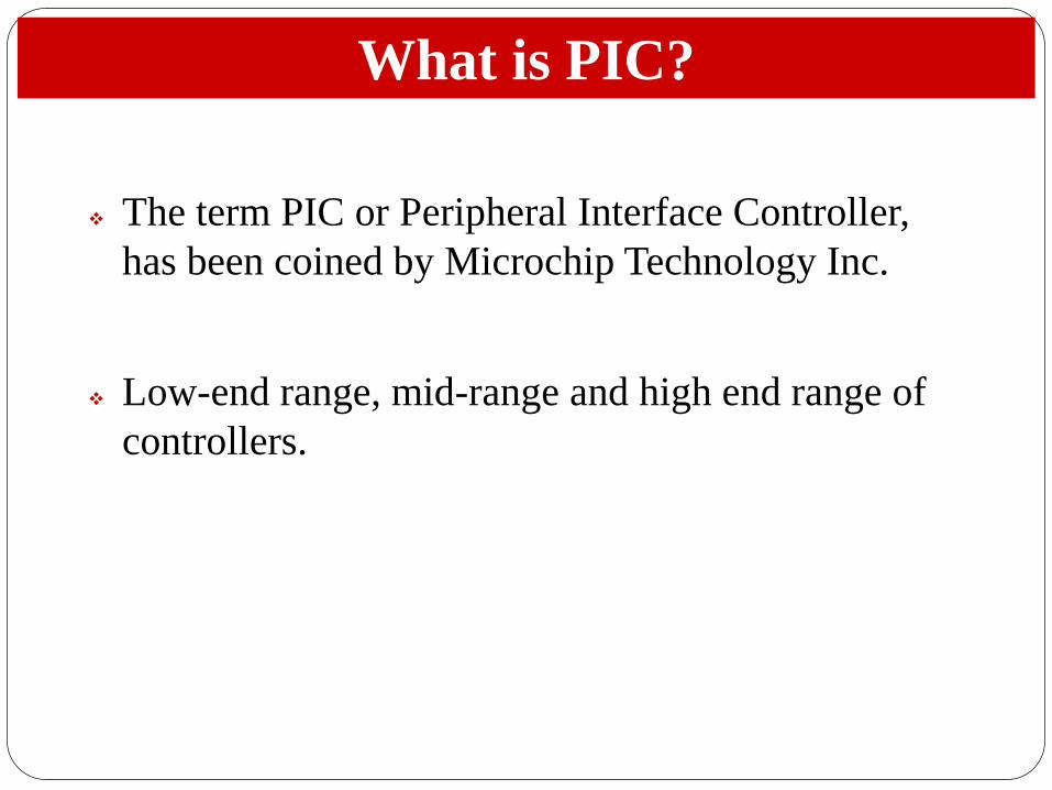
The term PIC or Peripheral Interface Controller,
has been coined by Microchip Technology Inc.
Low-end range, mid-range and high end range of
controllers.
What is PIC?

We’re used to the Von-Neuman Architecture
Used in: 80X86 (PCs), 8051, 68HC11, etc.)
Only one bus between CPU and memory
RAM and program memory share the same bus and
the same memory, and so must have the same bit
width
Bottleneck: Getting instructions interferes with
accessing RAM
CPU 8
Memory
(& Data)
PIC Architecture: Background

PICs use the Harvard Architecture
Used mostly in RISC CPUs (we’ll get there)
Separate program bus and data bus: can be different
widths!
For example, PICs use:
Data memory (RAM): a small number of 8bit
registers
Program memory (ROM): 12bit, 14bit or 16bit
wide (in EPROM, FLASH, or ROM)
CPU 12 14 16
Memory
(Data) 8
Memory
(Program)
PIC Architecture: Background

Traditionally, CPUs are “CISC”
Complex Instruction Set Computer (CISC)
Used in: 80X86, 8051, 68HC11, etc.
Many instructions (usually > 100)
Many, many addressing modes
Usually takes more than 1 internal clock cycle
(T cycle) to execute
Example:
MC68HC05: LDAA 0x55
01010101
1000 1100 2 bytes, 2 cycles
CISC

PICs and most Harvard chips are “RISC”
Reduced Instruction Set Computer (RISC)
Used in: SPARC, ALPHA, Atmel AVR, etc.
Few instructions (usually < 50)
Only a few addressing modes
Executes 1 instruction in 1 internal clock cycle
(Tcyc)
Example:
PIC16CXXX: MOVLW 0x55
1 word, 1 cycle
1100XX 01010101
RISC
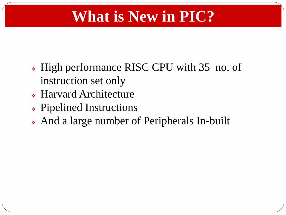
High performance RISC CPU with 35 no. of
instruction set only
Harvard Architecture
Pipelined Instructions
And a large number of Peripherals In-built
What is New in PIC?

Pin Diagram

8kB of flash program
memory
368bytes of Data
memory
256-EEPROM data
memory
15 Interrupts
In-circuit programming
3 internal hardware
timers
Capture/Compare/PW
M modules
Up to 8 channels of 10-
Bit A/D
Built-in USART for
serial communication
5 digital I/O ports (Up
to 22 lines)
Features

PIC 16F877A has FIVE I/O Ports
A total of 33 pins are used for I/O operations.
PORT A
Port A is 6 bit wide and bi-directional.
Its corresponding data direction register is TRISA.
If TRISA port pin is set to 1,corresponding port A pin
will act as an input pin and vice versa.
Port A is used for analog inputs.
I/O Ports
Port B is 8 bit wide and bi-directional.
Its corresponding data direction register is TRISB.
If TRISB port pin is set to 1,corresponding port B
pin will act as an input pin and vice versa.
Port B is used for Data Transmission.
Port B

Port C is 8 bit wide and bi-directional.
Its corresponding data direction register is TRISC.
If TRISC port pin is set to 1,corresponding port C
pin will act as an input pin and vice versa.
Port C is used for control registers(serial
communication, I2C functions,serial data transfer).
Port C

Port D is 8 bit wide and bi-directional.
Its corresponding data direction register is
TRISD.
If TRISD port pin is set to 1,corresponding port D
pin will act as an input pin and vice versa.
Port D is used as Data port
Port D

Port E is 3 bit wide . They are for read, write and
chip select operation.
Each pin is individually configurable as inputs
and outputs.
Port E is generally used for controlling purposes.
Port E
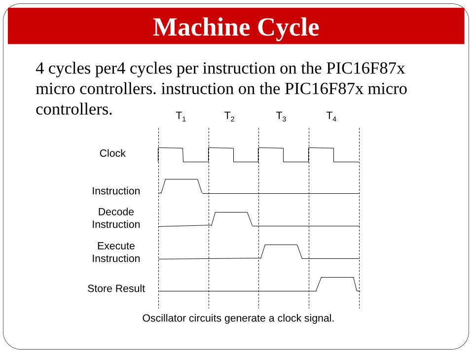
4 cycles per4 cycles per instruction on the PIC16F87x
micro controllers. instruction on the PIC16F87x micro
controllers.
Clock
Read
Instruction
Decode
Instruction
Execute
Instruction
Store Result
T1 T2 T3 T4
Oscillator circuits generate a clock signal.
Machine Cycle
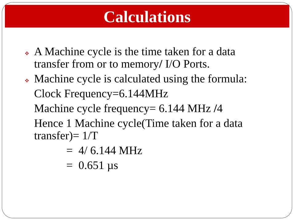
A Machine cycle is the time taken for a data transfer from or to memory/ I/O Ports.
Machine cycle is calculated using the formula:
Clock Frequency=6.144MHz
Machine cycle frequency= 6.144 MHz /4
Hence 1 Machine cycle(Time taken for a data transfer)= 1/T
= 4/ 6.144 MHz
= 0.651 µs
Calculations

An instruction cycle is the time taken to complete
an instruction.
All instructions in 16F877A are single cycle
instructions except for Branching instruction. They
take two machine cycles to complete an
instruction.
Instruction Cycle

Different PICs have different on-board peripherals some
common peripherals are:
3 Timers (0 & 2- 8bits, 1-16 bits)
2 Compare/Capture/PWM Modules
Analog to Digital Converters (ADC) (8, 10 and 12bit,
50ksps)
Serial communications: UART (RS-232C), SPI, I2C,
CAN
Pulse Width Modulation (PWM) (10bit)
Voltage Comparators
Voltage Reference Modules
MSSP – Master Synchronous Serial Port
I2C (Master and Slave)
SPI (Master and Slave)
Watchdog timers, Brown out detect, LCD drivers
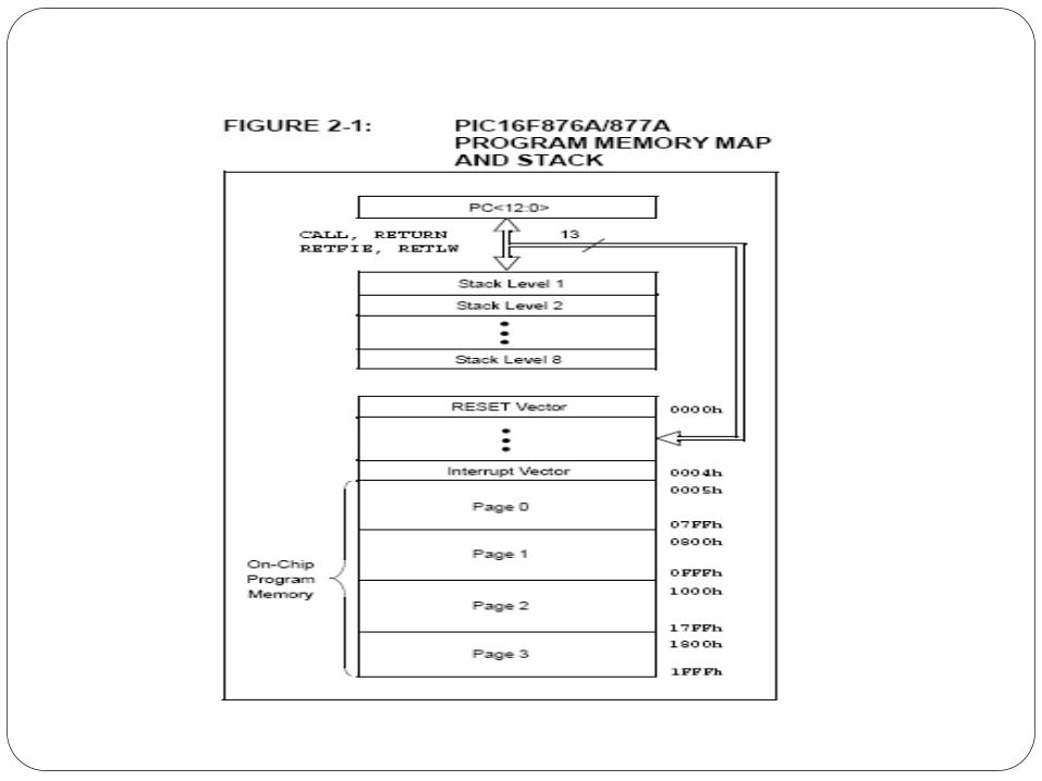
PIC overview
Instructions
Memory Organisation
Overview
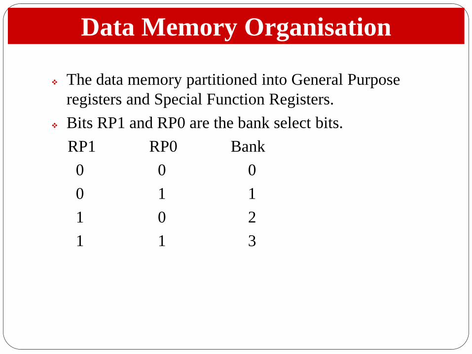
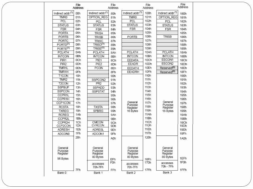
The data memory partitioned into General Purpose
registers and Special Function Registers.
Bits RP1 and RP0 are the bank select bits.
RP1 RP0 Bank
0 0 0
0 1 1
1 0 2
1 1 3
Data Memory Organisation
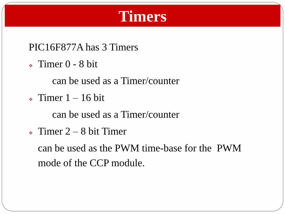
PIC16F877A has 3 Timers
Timer 0 - 8 bit
can be used as a Timer/counter
Timer 1 – 16 bit
can be used as a Timer/counter
Timer 2 – 8 bit Timer
can be used as the PWM time-base for the PWM
mode of the CCP module.
Timers


The data registers of Timer 1 are TMR1H and TMR1L.
The 16 bit value to be loaded in the timer is given to
Data registers
The Control register is T1CON.
The timer ON and oscillator enable operations are
controlled through the control register.
To determine if the timer has completed its operation,
the timer overflow bit TMR1IF of the PIR1 register is
checked continuously.
Timer 1

Universal synchronous asynchronous receiver
transmitter is also known as a serial
communication interface.
USART can be configured in the following
modes:
Asynchronous - FULL DUPLEX
synchronous - HALF DUPLEX
USART
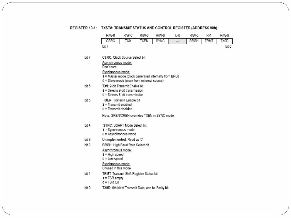
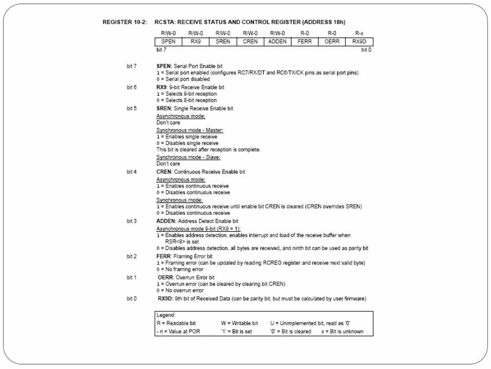
For serial Communication, the SFR involved are
TXSTA, TXREG, RCSTA,,RCREG and SPBRG.
SPBRG is used to set the required baud rate.
In TXSTA,TXEN is set high to enable
transmission.
The transmitted data is stored in a temporary
buffer,TXREG.
In RCSTA, SPEN and CREN are set high to enable
reception.
The received data is stored in a temporary buffer,
RCREG.
Serial Communication

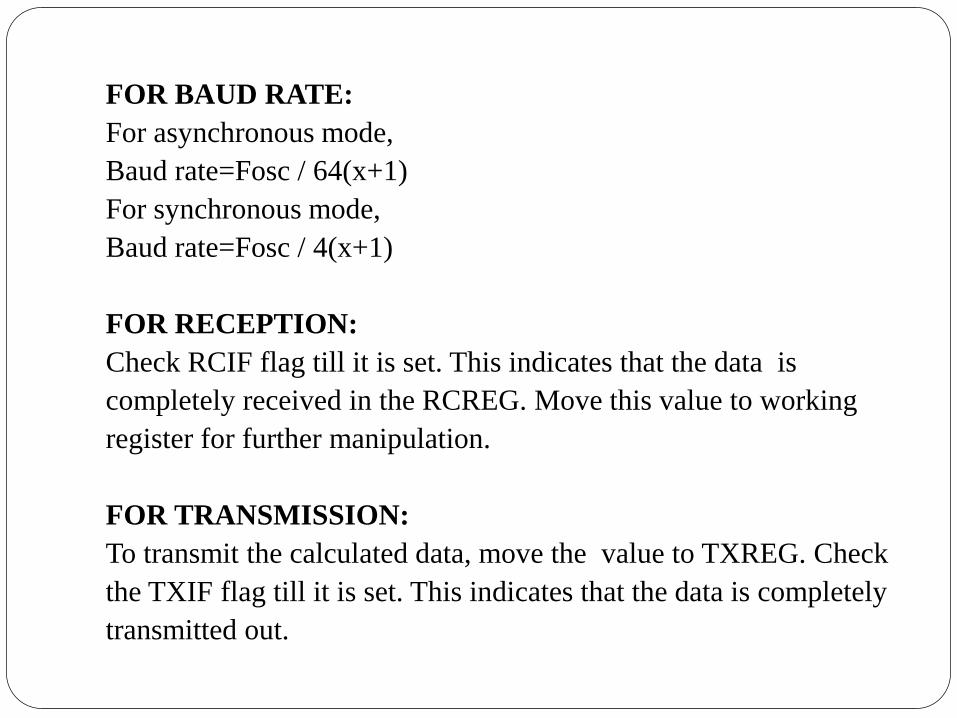
FOR BAUD RATE:
For asynchronous mode,
Baud rate=Fosc / 64(x+1)
For synchronous mode,
Baud rate=Fosc / 4(x+1)
FOR RECEPTION:
Check RCIF flag till it is set. This indicates that the data is
completely received in the RCREG. Move this value to working
register for further manipulation.
FOR TRANSMISSION:
To transmit the calculated data, move the value to TXREG. Check
the TXIF flag till it is set. This indicates that the data is completely
transmitted out.


PIC16F877A has 15 sources of interrupts.
Only one vector location is allocated for the
interrupts.
The Global interrupt enable bit is set, so that any
interrupt can be acknowledged.
Regardless of the Global enable bit, the user
should ensure,the appropriate interrupt flag bits
that needs to be executed, is also set.
Interrupts

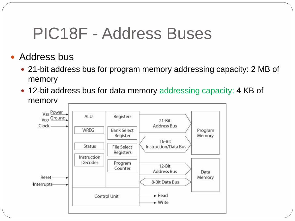
PIC18F - Address Buses
Address bus
21-bit address bus for program memory addressing capacity: 2 MB of
memory
12-bit address bus for data memory addressing capacity: 4 KB of
memory

Data Bus and Control Signals
• Data bus – 16-bit instruction/data bus for program memory
– 8-bit data bus for data memory
• Control signals – Read and Write

PIC18F452/4520 Memory
Program memory with
addresses (Flash)
Data memory with
addresses
FFF=212=16x256=4096=4K

Program Memory
A 21-bit program counter is capable of addressing the 2-
Mbyte program memory space.
Accessing a location between the physically implemented memory
and the 2-Mbyte address will cause a
read of all ’0’s (a NOP instruction).
PIC18F452 each have 32 Kbytes of FLASH memory. This means that it can store up to 16K of single word instructions
The RESET vector address is at 0000h and the interrupt vector addresses are at 0008h and 0018h.

Access RAM
Data Memory Organization PIC16F8F2520/4520 Register File Map
000h
07Fh
256 Bytes
Bank 0 GPR
Bank 1 GPR
Bank 2 GPR
Bank 13 GPR
Bank 14 GPR
Bank 15 GPR
Access SFR
Access RAM
Access SFR
080h
0FFh
100h
1FFh
200h
2FFh
D00h
DFFh
E00h
EFFh
F00h
FFFh
F7Fh
F80h
00h
7Fh
80h
FFh
Access Bank
Data Memory up to 4k
bytes
Divided into 256 byte banks
Half of bank 0 and half of
bank 15 form a virtual bank
that is accessible no matter
which bank is selected
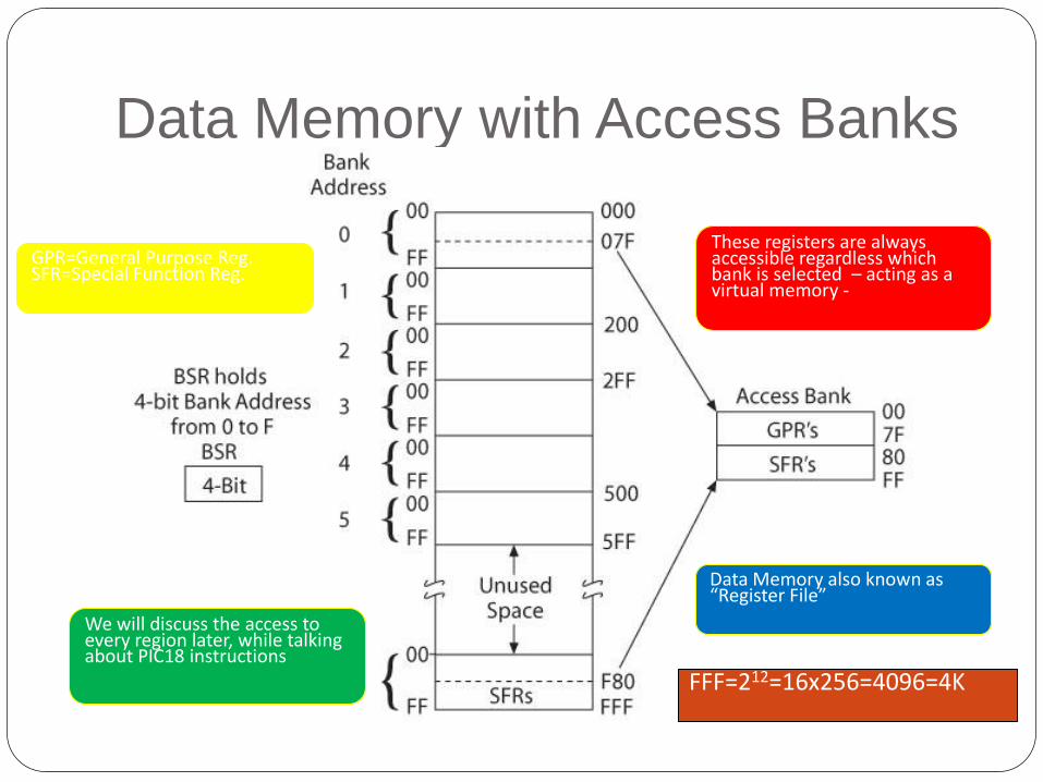
Data Memory with Access Banks
FFF=212=16x256=4096=4K
GPR=General Purpose Reg. SFR=Special Function Reg.
These registers are always accessible regardless which bank is selected – acting as a virtual memory -
Data Memory also known as “Register File”
We will discuss the access to every region later, while talking about PIC18 instructions
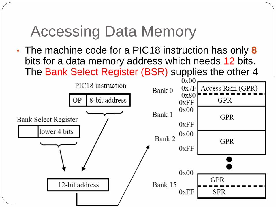
Accessing Data Memory • The machine code for a PIC18 instruction has only 8
bits for a data memory address which needs 12 bits. The Bank Select Register (BSR) supplies the other 4 bits.
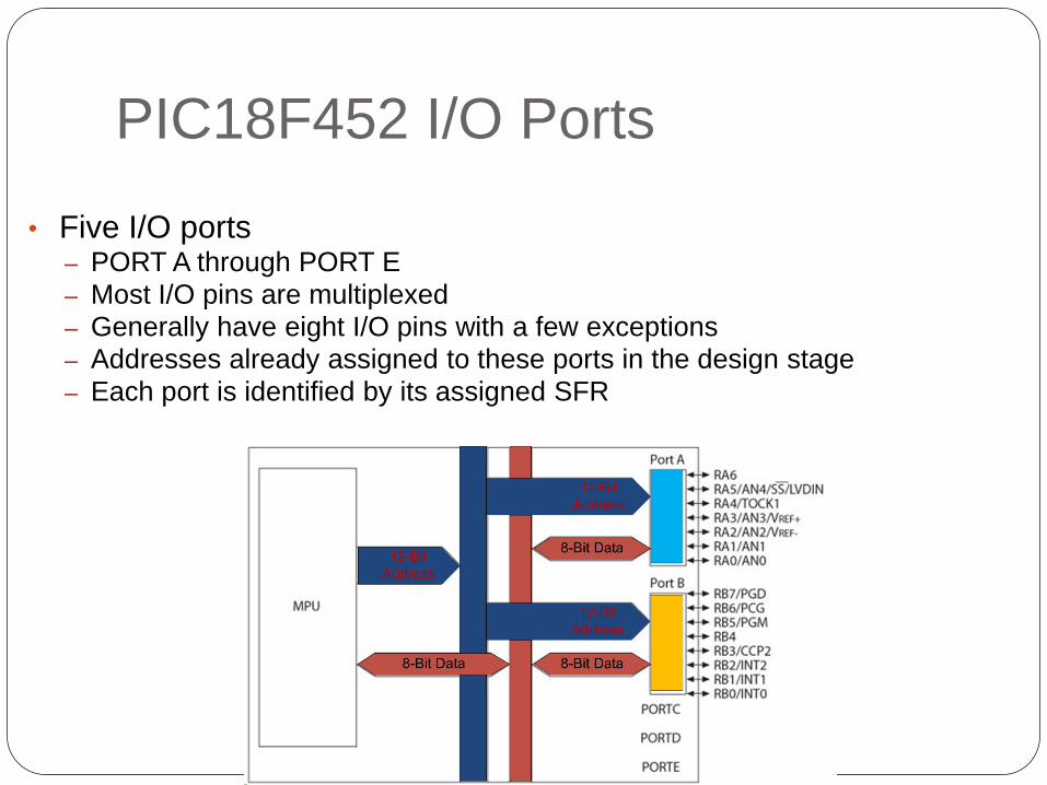
PIC18F452 I/O Ports
• Five I/O ports – PORT A through PORT E
– Most I/O pins are multiplexed – Generally have eight I/O pins with a few exceptions – Addresses already assigned to these ports in the design stage
– Each port is identified by its assigned SFR
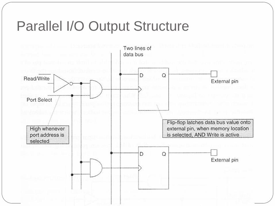
Parallel I/O Output Structure
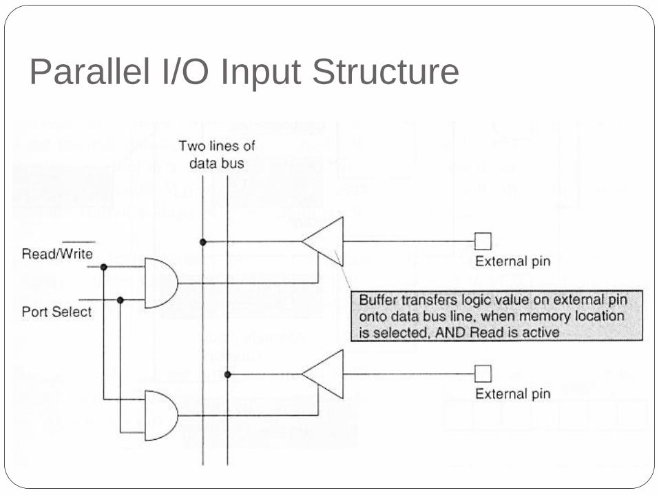
Parallel I/O Input Structure

Parallel I/O Combined I/O Structure

Parallel I/O ports Main Features
Simple memory mapped access
Can be configured through software as either input or output
Ability to set or reset individual bits
Can have internal pull-ups
Can drive small loads like LEDs
Can be multifunction
Different capability for pins (i.e. larger current)

Parallel I/O ports
For most ports, the I/O pin’s direction (input or output) is controlled by the data direction register TRISx (x=A,B,C,D,E): a ‘1’ in the TRIS bit corresponds to that pin being an input, while a ‘0’ corresponds to that pin being an output
The PORTx register is the latch for the data to be output. Reading PORTx register read the status of the pins, whereas writing to it will write to the port latch.
Example: Initializing PORTB (PORTB is an 8-bit port. Each pin is individually configurable as an input or output).
bcf STATUS, RP0 ; select bank0
bcf STATUS, RP1
clrf PORTB ; clear PORTB output data latches
bsf STATUS, RP0 ; select bank1
movlw 0xCF ; value used to initialize data direction
movwf TRISB ; PORTB<7:6>=inputs, PORTB<5:4>=outputs,
; PORTB<3:0>=inputs
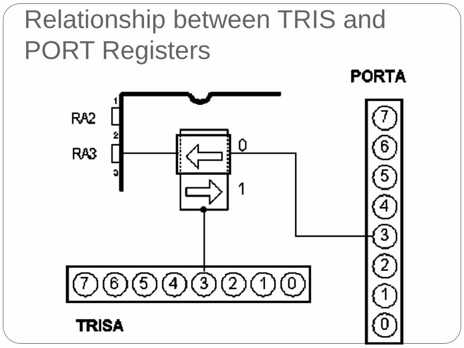
Relationship between TRIS and
PORT Registers

Illustration: Displaying a Byte
at an I/O Port (1 of 5)
Problem statement:
Write instructions to light up alternate LEDs at
PORTC.
Hardware:
PORTC
bidirectional (input or output) port; should be setup as
output port for display
Logic 1 will turn on an LED in Figure 2.10.

Illustration (2 of 5)
Interfacing LEDs to
PORTC
Port C is F82H
Note that PORT C
is set to be an
output!
Hence, TRISC
(address 94H) has
to be set to 0
TRISC=0
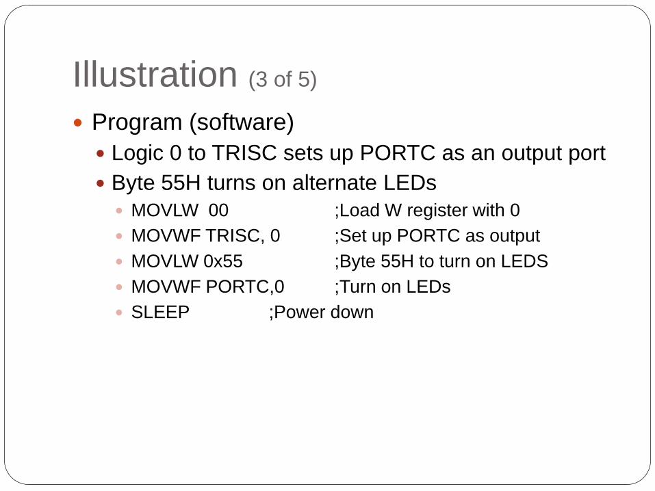
Illustration (3 of 5)
Program (software)
Logic 0 to TRISC sets up PORTC as an output port
Byte 55H turns on alternate LEDs
MOVLW 00 ;Load W register with 0
MOVWF TRISC, 0 ;Set up PORTC as output
MOVLW 0x55 ;Byte 55H to turn on LEDS
MOVWF PORTC,0 ;Turn on LEDs
SLEEP ;Power down