
Architecture of pentium family
61
Architecture of pentium family GROUP 6 • 12063122-071 Humayun • 12063122-039 AB Mir • 12063122-047 Nawazish • 12063122-025 AAmir • 12063122-073 Iqtadar 2/3/2015 copyright 2006 www.brainybetty.com; All Rights Reserved. 1
-
Upload
university-of-gujrat-pakistan -
Category
Engineering
-
view
291 -
download
1
Transcript of Architecture of pentium family

Architecture of pentium family
GROUP 6
• 12063122-071 Humayun
• 12063122-039 AB Mir
• 12063122-047 Nawazish
• 12063122-025 AAmir
• 12063122-073 Iqtadar
2/3/2015 copyright 2006 www.brainybetty.com; All Rights Reserved. 1

• Architecture Of
Pentium Family
2/3/2015 copyright 2006 www.brainybetty.com; All Rights Reserved. 2
Introduction
• The knowledge acquired here about the Pentium processor features, architecture, signals and key bus cycles will serve a foundation for the boards based on this processor.
• This overview will describe the features of the Pentium as used in a typical Single Processor PC system in Real Mode.
OBJECTIVES:
• Describe the basic architecture of the Pentium
processor.
• Explain the use of the Pentium Registers.
• Describe the various Pentium buses.
• Explain the use of the Byte Enables .
• Discuss Pentium address generation.
• Discuss Pentium Bus Cycle Definitions.
• Discuss Pentium Signal Descriptions.

Pentium Processor
Architecture

Pentium Processor Architecture
Divide
Add
64 bit bus
Interface
Code Cache
Prefetch
Buffers
Integer
ALU
Integer
ALU
Register Set
Data Cache
Branch
Prediction
Pipelined
Floating-Point
Unit
Multiply
U pipe V pipeline
32 bits
64 bits
256 bits

Pentium Processor Architecture
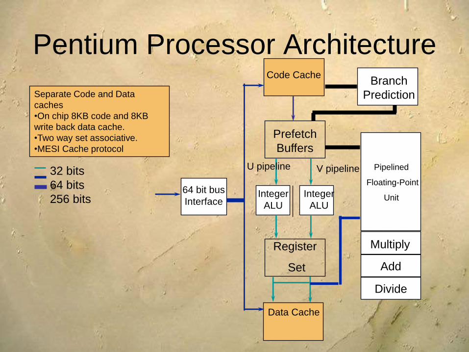
• The Pentium processors have a data bus of 64 bits.– This is a 32 bit CPU due to having 32 bits registers.
– A standard Single Transfer Cycle can read or write up to 64 bits at a time (8 bytes)
• Burst read and burst write-back cycles are supported by the Pentium processors.– Burst Mode cycles are used for Cache operations and
transfer 32 bytes in 4 clocks (4 * 8 bytes = 4 * 64 bits).• 32 bytes is the size of the Pentium Cache line.
– For the Pentium, all cache operations are burst cycles.
32 bits
64 bits
256 bits
Separate Code and Data
caches
•On chip 8KB code and 8KB
write back data cache.
•Two way set associative.
•MESI Cache protocol
Divide
Add
64 bit bus
Interface
Prefetch
Buffers
Code Cache
Integer
ALU
Integer
ALU
Register
Set
Data Cache
Branch
Prediction
Pipelined
Floating-Point
Unit
Multiply
U pipeline V pipeline
Pentium Processor Architecture
Pentium Processor Architecture
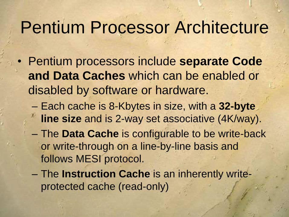
• Pentium processors include separate Code
and Data Caches which can be enabled or
disabled by software or hardware.
– Each cache is 8-Kbytes in size, with a 32-byte
line size and is 2-way set associative (4K/way).
– The Data Cache is configurable to be write-back
or write-through on a line-by-line basis and
follows MESI protocol.
– The Instruction Cache is an inherently write-
protected cache (read-only)

Divide
Add
64 bit bus
Interface
Code Cache
Prefetch
Buffers
Integer
ALU
Integer
ALU
Register Set
Data Cache
Branch
Prediction
Pipelined
Floating-Point
Unit
Multiply
U pipeline V pipeline
32 bits
64 bits
256 bits
Pipeline
sequence
Prefetch
Decode1
Decode2
Execute
Write Back
•Branch prediction:
Processor makes
predictions on next
instruction to be executed
via the BTB.
Hardwired
Instructions
Technical Innovations...
Pentium Processor Architecture
•Superscalar Architecture
•more than one execution
unit
NOTE: The Instruction
Decode Unit is in the
Prefetch Buffers on this
diagram.
Pentium Processor Architecture
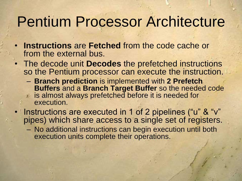
• Instructions are Fetched from the code cache or from the external bus.
• The decode unit Decodes the prefetched instructions so the Pentium processor can execute the instruction.– Branch prediction is implemented with 2 Prefetch
Buffers and a Branch Target Buffer so the needed code is almost always prefetched before it is needed for execution.
• Instructions are executed in 1 of 2 pipelines (“u” & “v” pipes) which share access to a single set of registers.– No additional instructions can begin execution until both
execution units complete their operations.
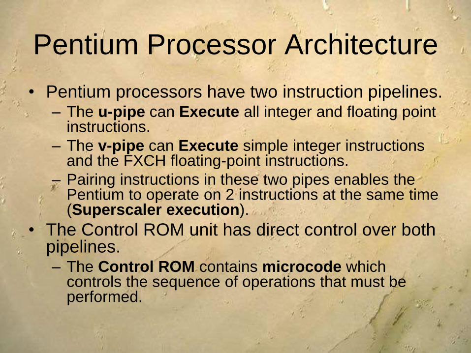
Pentium Processor Architecture
• Pentium processors have two instruction pipelines.– The u-pipe can Execute all integer and floating point
instructions.
– The v-pipe can Execute simple integer instructions and the FXCH floating-point instructions.
– Pairing instructions in these two pipes enables the Pentium to operate on 2 instructions at the same time (Superscaler execution).
• The Control ROM unit has direct control over both pipelines.– The Control ROM contains microcode which
controls the sequence of operations that must be performed.

Pentium
Processor
Registers

Pentium Registers07152331 16-BIT 32-BIT
AX
DX
CX
BX
EAX
EDX
ECX
EBX
EBP
ESI
EDI
ESP
Segment Registers
General Registers
16 8
CS
SS
DS
ES
FS
GS
AH
DH
CH
BH
AL
DL
CL
BL
EFLAGS
EIP
Status and Control
031
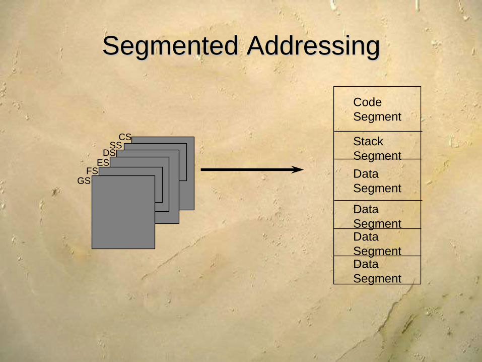
Segmented Addressing
Code
Segment
Stack
Segment
Data
Segment
Data
Segment
Data
Segment
Data
Segment
CS
DSSS
ESFS
GS

Segmented Addressing
Segment Register
Offset within segment0
15
15
0
Operand
e.g - CS
e.g - IP
NOTE: We will assume,
unless otherwise stated,
that all examples reflect
real mode.
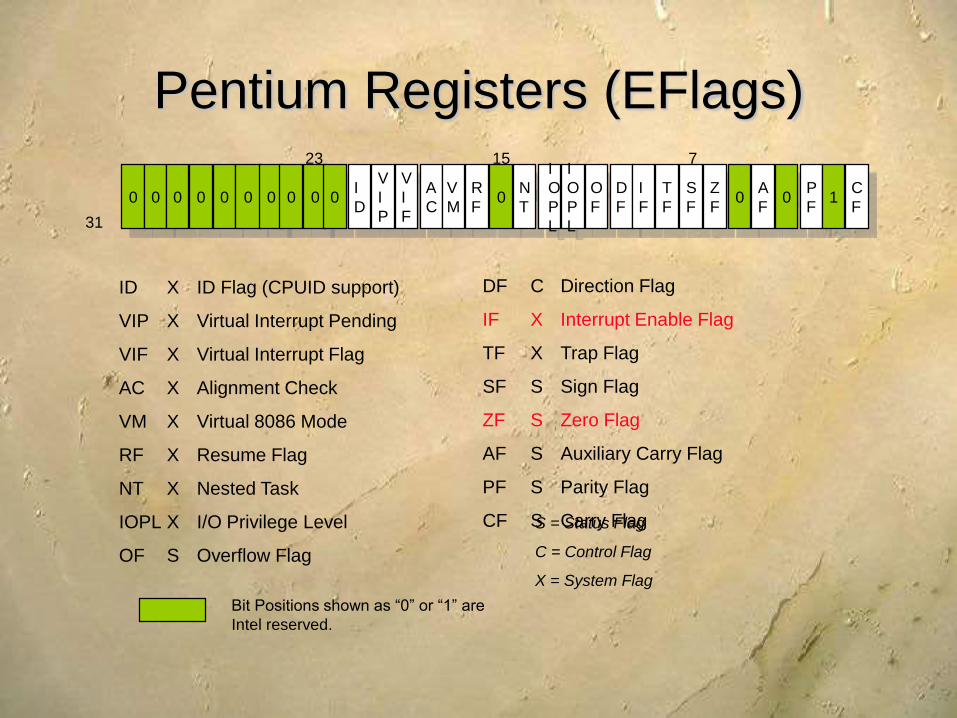
Pentium Registers (EFlags)
• The EFlags register is not a normal register but a collection of FLAG BITS which indicate the result of previous operations or the current state of the CPU.– A FLAG is just a flip-flop in the CPU that is SET (1) or
RESET (0) [cleared] depending on the condition produced by an instruction .
– Some Flags indicate the condition produced by the previous instruction.
• e.g - Zero Flag: ZF=1 (True) if the result of the last arithmetic or logical operation was Zero.
– Some Flags are used to control certain operations.• e.g. - IF (Interrupts Enabled); Trap Flag; Direction Flag.
Pentium Registers (EFlags)
ID X ID Flag (CPUID support)
VIP X Virtual Interrupt Pending
VIF X Virtual Interrupt Flag
AC X Alignment Check
VM X Virtual 8086 Mode
RF X Resume Flag
NT X Nested Task
IOPL X I/O Privilege Level
OF S Overflow Flag
DF C Direction Flag
IF X Interrupt Enable Flag
TF X Trap Flag
SF S Sign Flag
ZF S Zero Flag
AF S Auxiliary Carry Flag
PF S Parity Flag
CF S Carry FlagS = Status Flag
C = Control Flag
X = System Flag
Bit Positions shown as “0” or “1” are
Intel reserved.
31 0
0 0 0 0 0 0 0 0 0 0I
D
V
I
P
V
I
F
A
C
V
M
R
F0
N
T
I
O
P
L
I
O
P
L
O
F
D
F
I
F
T
F
S
F
Z
F0
A
F0
P
F
23
1
15 7
C
F

Pentium Registers (Debug)
B
3
B
2
B
1
B
0
B
T
B
S
B
D
G
D
DR3 - Breakpoint 3 Linear Address
DR2 - Breakpoint 2 Linear Address
DR1 - Breakpoint 1 Linear Address
DR0 - Breakpoint 0 Linear Address
LEN
3
R/W
3
LEN
2
R/W
2
R/W
1
R/W
0
LEN
1
LEN
0
G
E
L
E
G
3
L
3
G
2
L
2
G
1
L
1
G
0
L
0
1 1 1 1 1 1 1 1 1 1 1 1 1 1 1 1 0 1 1 1 1 1 1 1 1
0 0 10 0
Reserved
Reserved

Pentium Registers (Debug)
• The Debug Registers provide hardware support for setting breakpoints.
• You can define up to four breakpoints using Debug Registers (DR0 - DR3).
• The Debug Registers store the Linear Address.– The linear address is the address after the addition of
the Segment Base & the Offset (w/o Paging). • This is the Physical Address in REAL MODE.
• When the Pentium address matches an address in one of the Debug Registers, the Pentium issues a Debug Exception (INT 1).– This feature is used with the ITP Debug Tool.

Pentium Bus
Description

Bus Description
Byte
Low
Byte
High
Byte
Low WordHigh Word
Low DoublewordHigh Doubleword
07
01531
0715
31
Address N
Address
N+1Address
N
Address
N
Address
N+1Address
N+2Address
N+3
0154763
Byte
Word
Doubleword
Address
N
Address
N+1Address
N+2
Address
N+3
Address
N+4
Address
N+5Address
N+6
Address
N+7
Data Types
Each location in
memory is Byte wide
Quadword
“Chunk”
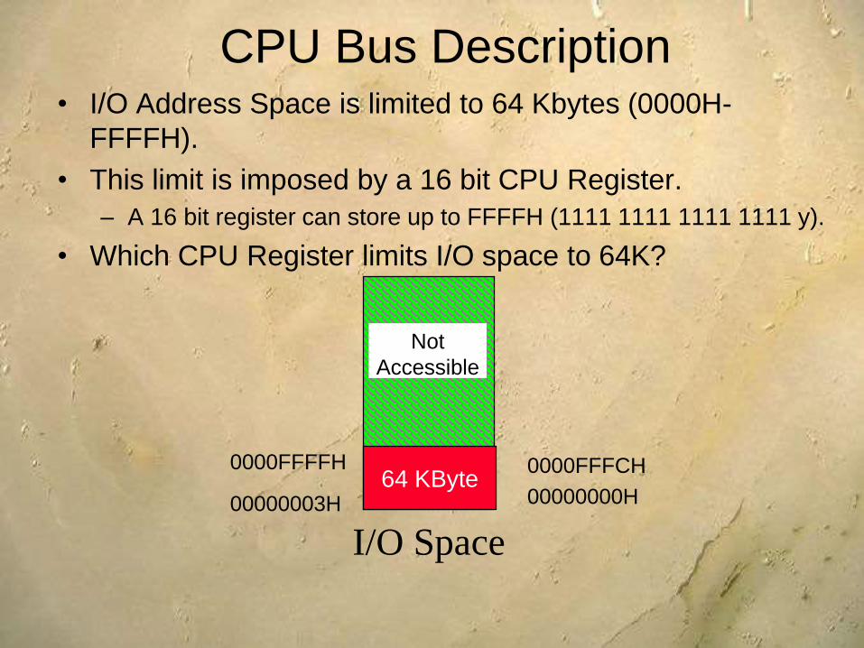
CPU Bus Description• I/O Address Space is limited to 64 Kbytes (0000H-
FFFFH).
• This limit is imposed by a 16 bit CPU Register.
– A 16 bit register can store up to FFFFH (1111 1111 1111 1111 y).
• Which CPU Register limits I/O space to 64K?
00000000H00000003H
I/O Space
64 KByte
Not
Accessible
0000FFFCH0000FFFFH
CPU Bus Description
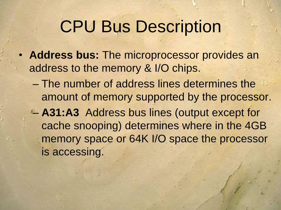
• Address bus: The microprocessor provides an
address to the memory & I/O chips.
– The number of address lines determines the
amount of memory supported by the processor.
– A31:A3 Address bus lines (output except for
cache snooping) determines where in the 4GB
memory space or 64K I/O space the processor
is accessing.
CPU Bus Description
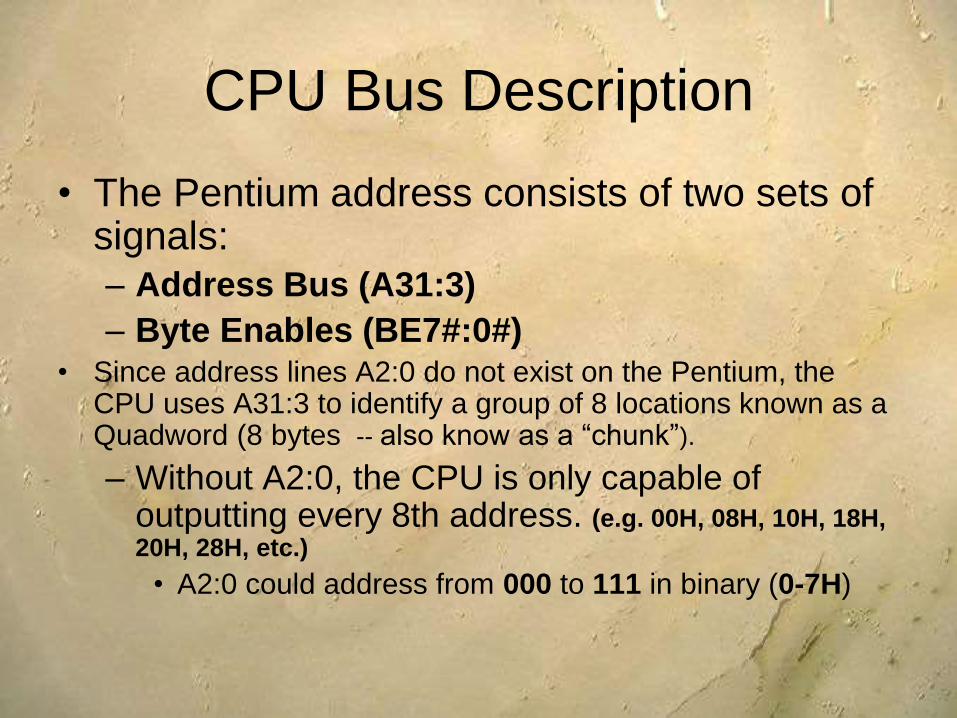
• The Pentium address consists of two sets of signals:
– Address Bus (A31:3)
– Byte Enables (BE7#:0#)• Since address lines A2:0 do not exist on the Pentium, the
CPU uses A31:3 to identify a group of 8 locations known as a Quadword (8 bytes -- also know as a “chunk”).
– Without A2:0, the CPU is only capable of outputting every 8th address. (e.g. 00H, 08H, 10H, 18H, 20H, 28H, etc.)
• A2:0 could address from 000 to 111 in binary (0-7H)
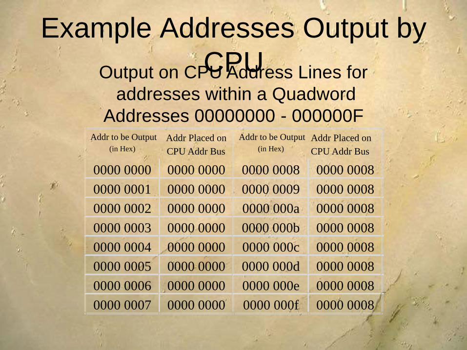
Addr to be Output
(in Hex)
Addr Placed on
CPU Addr Bus
Addr to be Output
(in Hex)
Addr Placed on
CPU Addr Bus
0000 0000 0000 0000 0000 0008 0000 0008
0000 0001 0000 0000 0000 0009 0000 0008
0000 0002 0000 0000 0000 000a 0000 0008
0000 0003 0000 0000 0000 000b 0000 0008
0000 0004 0000 0000 0000 000c 0000 0008
0000 0005 0000 0000 0000 000d 0000 0008
0000 0006 0000 0000 0000 000e 0000 0008
0000 0007 0000 0000 0000 000f 0000 0008
Example Addresses Output by
CPUOutput on CPU Address Lines for
addresses within a Quadword
Addresses 00000000 - 000000F
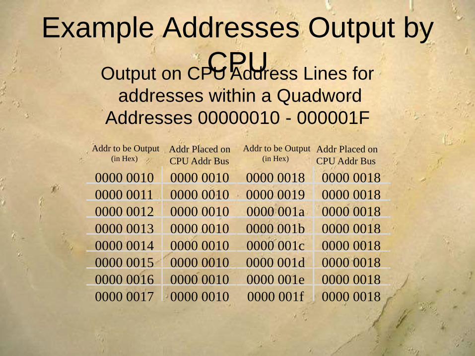
Example Addresses Output by
CPU
Addr to be Output(in Hex)
Addr Placed on
CPU Addr Bus
Addr to be Output(in Hex)
Addr Placed on
CPU Addr Bus
0000 0010 0000 0010 0000 0018 0000 0018
0000 0011 0000 0010 0000 0019 0000 0018
0000 0012 0000 0010 0000 001a 0000 0018
0000 0013 0000 0010 0000 001b 0000 0018
0000 0014 0000 0010 0000 001c 0000 0018
0000 0015 0000 0010 0000 001d 0000 0018
0000 0016 0000 0010 0000 001e 0000 0018
0000 0017 0000 0010 0000 001f 0000 0018
Output on CPU Address Lines for
addresses within a Quadword
Addresses 00000010 - 000001F

CPU Bus Description
• The Pentium uses Byte Enables to address locations within a QWORD.
– BE7#:BEO# (outputs): Byte enable lines - to enable each of the 8 bytes in the 64-bit data path.
– In effect a decode of the address lines A2-A0 which the Pentium does not generate.
– Which lines go active depends on the address, and whether a byte, word, double word or quad word is required.

Relationship of Byte Enables to
Locations Addressed within a QWORD
Byte Enable Data Path Used Location in Qword
BE0# D07:00 FIRST
BE1# D15:08 SECOND
BE2# D23:16 THIRD
BE3# D31:24 FOURTH
BE4# D39:32 FIFTH
BE5# D47:40 SIXTH
BE6# D55:48 SEVENTH
BE7# D63:56 EIGHT
CPU Bus Description
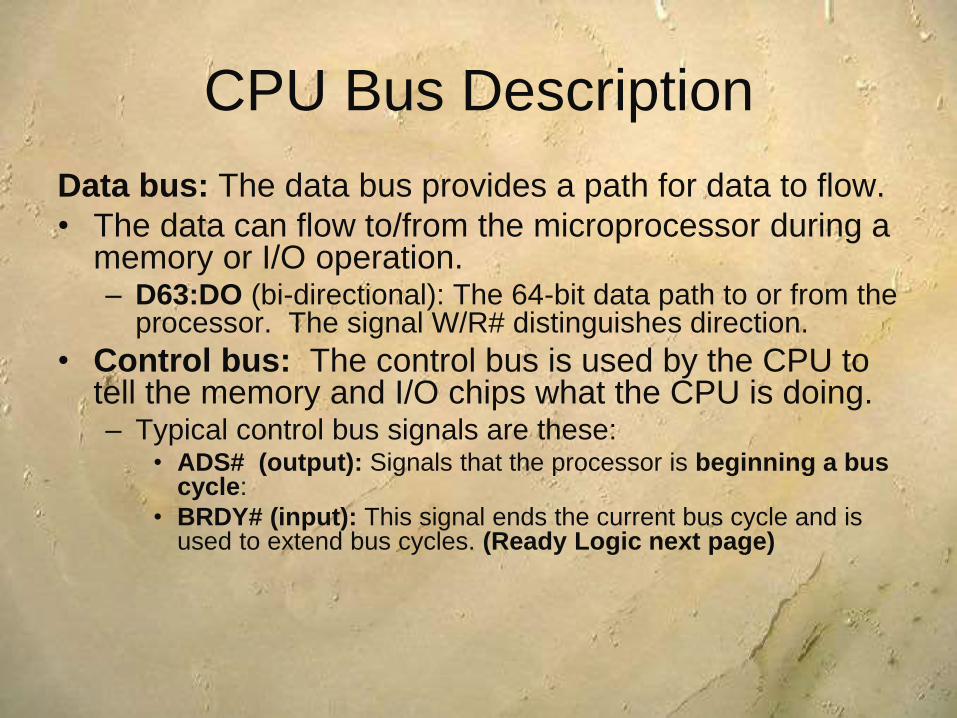
Data bus: The data bus provides a path for data to flow.
• The data can flow to/from the microprocessor during a memory or I/O operation. – D63:DO (bi-directional): The 64-bit data path to or from the
processor. The signal W/R# distinguishes direction.
• Control bus: The control bus is used by the CPU to tell the memory and I/O chips what the CPU is doing.– Typical control bus signals are these:
• ADS# (output): Signals that the processor is beginning a bus cycle:
• BRDY# (input): This signal ends the current bus cycle and is used to extend bus cycles. (Ready Logic next page)

CPU Bus Description
• Control bus:(Cont.)
– Typical control bus signals are these: (Cont.)• M/IO# (output): Defines if the bus cycle is a Memory
access or an Input/Output Port access.
• D/C# (output): Defines if the bus cycles is Data or Code for Memory access.
• W/R# (output): Indicates if bus cycle is a Write or a Read operation.
• Cache#. (output): Processor indication of internal cacheability. Cache# and Ken# are used together to determine of a read will be turned into a linefill. (Burst cycle).

Pentium Signal
Description
Pentium Signal Description
• This overview will describe the signals
of the Pentium as used in a typical
Single Processor PC system.

Signal DescriptionClock
Initialization
Address Bus
Address Mask
Data Bus
Address Parity
Data Parity
Bus Cycles Definition
Bus Control
Cache Control
Cache Snooping
Cache Flush
Bus Arbitration
Interrupts
FP Error Reporting
SMM
Probe Mode
TAP Port
Internal Parity Error
Pentium
Signal Description
• CLOCK
– CLK - Clock (Input)• Fundamental Timing for the Pentium
• The CPU uses this signal as the internal processor clock.
– BF - Bus Frequency (Input)• Bus Frequency determines the bus-to-core frequency ratio
• When BF is strapped to Vcc, the processor will operate at a 2 to 3 bus to core frequency ratio.
• When BF is strapped to Vss, the processor will operate at a 1 to 2 bus to core frequency ratio.
• What symptoms might be exhibited if this signal is incorrect?

Signal Description
• Initialization
– RESET - (Input)
• Forces the CPU to begin execution at a known
state.
– INIT - Initialization (Input)
• The Pentium processor initialization input pin
forces the Pentium processor to begin execution
in a known state.
• The processor state after INIT is the same as the
state after RESET except that the internal caches,
write buffers, and floating point registers retain the
values they had prior to INIT.
Signal Description
• Address Bus
– A31:A3 - ADDRESS bus lines
• Output except for cache snooping
– The number of address lines determines the
amount of memory supported by the
processor.
– Determines where in the 4GB memory space
or 64K IO space the processor is accessing.
– These are input lines when AHOLD & EADS#
are active for Inquire Cycles (snooping)

Signal Description
• Address Bus– BE7#:BEO#: Byte Enable lines (Outputs)
– Byte Enables to enable each of the 8 bytes in the 64-bit data path.
• Helps define the physical area of memory or I/O accessed.
• The Pentium uses Byte Enables to address locations within a QWORD.
• In effect a decode of the address lines A2-A0 which the Pentium does not generate.
• Which lines go active depends on the address, and whether a byte, word, double word or quad word is required.

Signal Description
• Address Mask– A20M#: Address 20 Mask (Input)
• Emulates the address wraparound at 1 MByte which occurs on the 8086.
• When A20M# is asserted, the Pentium processor masks physical address bit 20 (A20) before performing a lookup to the internal caches or driving a memory cycle on the bus.
• A20#M must be asserted only when the processor is in real mode.
• Internal Parity– IERR# - Internal Error (Output)
• Alerts System of Internal Parity Errors

Signal Description
• Address Parity– AP Address Parity (I/O)
• Bi-directional address parity pin for the address lines.
• Address Parity is driven by the Pentium processor with even parity information on all CPU generated cycles in the same clock that the address is driven
• Even parity must be driven back to the CPU during inquire cycles on this pin in the same clock as EADS#.
• Not supported on all systems
– APCHK#: Address Parity Check Signal (Output)• The status of the address parity check is driven on the
APCHK# output.
• Even Parity Checking

Signal Description
• Data Bus.
– D63:DO - Data Lines (I/O). • The bi-directional 64-bit data path to or from the CPU.
• The signal W/R# distinguishes direction.
• During reads, the CPU samples the data bus when BRDY# is asserted.
– DP7: DP0 - Data Parity (I/O)• Bi-directional data parity pins for the data bus.
• Even Parity Check. One for each byte of the data bus
• Output on writes, Input on reads.
• Not supported on all systems.
Signal Description
• Bus Control
– ADS# - Address Strobe (output)• Indicates that a new valid bus cycle is currently
being driven by the Pentium processor.
• The following are some of the signals which are valid when ADS#=0
– Addresses (A31:3)
– Byte Enables (BE7#:0#)
– Bus Cycle definition (M/IO#; D/C#; W/R#, CACHE#)
• From power-on the ADS# signal should be asserted periodically when bus cycles are running.
Signal Description
• Bus Control (Cont.)– BRDY# - Burst Ready (Input)
• Transfer complete indication.
• The burst ready input indicates that the external system has presented data on the data pins in response to a read or that the external system has accepted the Pentium processor data in response to a write request.
• This signal ends the current bus cycle and is used to extend bus cycles to allow slow devices extra time.
• If LOW (non-burst cycles), this signal ends the current bus cycle and the next bus cycle can begin.
• If HIGH the Pentium is prevented from continuing processing and wait states are added.

Signal Description
• Bus Cycle Definition
– M/IO# - Memory or Input/Output (output)
• M/IO# distinguishes between Memory and I/O
cycles.
• The memory/input-output is one of the primary bus
cycle definition pins.
– 1 = Memory Cycle
– 0 = Input/Output Cycle
• It is driven valid in the same clock as the ADS#
signal is asserted.

Signal Description
• Bus Cycle Definition (Cont.)
– D/C# - Data or Code (output)• D/C# distinguishes between data and code or
special cycles (control)
• The data/code output is one of the primary bus cycle definition pins.
– 1 = Data
– 0 = Code / Control
»Control for Interrupt Acknowledge or Special Cycles
• It is driven valid in the same clock as the ADS# signal is asserted.
Signal Description
• Bus Cycle Definition (Cont.)
– W/R# - Write or Read (output)
W/R# distinguishes between Write and Read cycles.
Write/read is one of the primary bus cycle definition pins.
• 1 = Write
• 0 = Read
It is driven valid in the same clock as the ADS# signal is asserted.

Bus Cycle Definition (Cont.)– Cache# - Cacheability (output)
• Processor indication of internal cacheability.
• The L1 cache must be enabled using the CD bit in CR0 for Cache# to be asserted low.
• The Cache# signal could also be described as the BURST instruction signal, because the Cache# signal (qualified with KEN#) results in a burst mode transfer of 32 bytes of code or data.
• Cache# and Ken# are used together to determine if aread will be turned into a linefill. (Burst cycle).
• During write-back cycles, the CPU asserts the CACHE# signal (KEN# does not have to be asserted)
Signal Description

Signal Description
• Bus Cycle Definition (Cont.)– NA# - Next Address (Input)
• Indicates external memory is prepared for a pipeline cycle.
• An active next address input indicates that the external memory system is ready to accept a new bus cycle although all data transfers for the current cycle have not yet completed.
• When NA# is asserted, the Pentium supplies the address for the start of the next transfer early, so that the memory system can latch the new address before the transfer is ready to start.
• A detailed discussion of Address Pipelining is beyond the scope of this course.

Signal Description
• Bus Cycle Definition (Cont.)– Lock# - Bus Lock (Output)
• The bus lock pin indicates that the current bus cycle is locked, typically for a read-modify-write operation.
• The CPU will not allow a bus hold when LOCK# is asserted.
• Locked cycles are generated when the programmer prefixes certain instructions with the LOCK prefix.
– e.g. LOCK INC [EDI] ;Increment a memory location
• Locked cycles are generated automatically for certain bus transfer operations.
– Interrupt Acknowledge cycles
– The XCHG instructions when 1 operand is memory-based.
– See Pentium manual for more details.
Signal Description
• Cache Control– KEN# - Cache Enable (Input)
• Indicates to the Pentium whether or not the system can support a cache line fill for the current cycle.
• Cache# and Ken# are used together to determine if aread will be turned into a linefill. (Burst cycle).
– WB/WT# - Write-back/Write-through (Input)• This pin allows a cache line to be defined as a a write
back or write-through on a line by line basis.
• This signal is necessary for the implementation of the MESI protocol.
• Detailed discussion of the MESI protocol is beyond the scope of this course.
Signal Description
• Cache Snooping
– AHOLD - Address Hold (Input)• Floats the address bus so an inquire cycle can be driven to
the Pentium.
• AHOLD allows another bus master (e.g. DMA ctlr) to drive the CPU address bus with the address for an inquire cycle.
– Effectively changes address lines to inputs.
• All other signals remain active so data for previously sent bus cycles can still be transferred.
– EADS# - External Address Strobe (Input)• Indicates that a valid external address has been driven onto
the CPU address pins for a snoop inquire cycle.
• Recognized while AHOLD is asserted.
Signal Description
• Cache Snooping (Cont.)
– HIT# - On Chip Cache hit (Output)
• Inquire Cycle Hit/Miss Indication
• Externally indicates whether an inquire cycle resulted in
a hit or miss.
– HITM# - On Chip Cache Hit Modified (Output)
• Hit/Miss to a modified line
• Externally indicates whether an inquire cycle hit a
modified line in the data cache.
• HITM# is never asserted without HIT# also being
asserted

• Cache Flush
– Flush# - Cache Flush (Input)
• Writes all modified lines in the data cache back
and flushes the code and data caches.
• A Flush Acknowledge special cycle will be
generated by the Pentium™ indicating completion
of the invalidation and writeback.
Signal Description
Signal Description
• Bus Arbitration– HOLD - Bus Hold (Input)
• Allows another bus master complete control of the CPU bus.
• In response to the bus hold request, the Pentium processor will float most of its output and input/output pins and assert HLDA after completing all outstanding bus cycles.
• The Pentium processor will maintain its bus in this state until HOLD is de-asserted.
– HLDA - Bus Hold Acknowledge (Output)• External indication that the Pentium™ outputs are
floated.
Signal Description
• Bus Arbitration (Cont.)
– BOFF# - Backoff (Input)• Forces the Pentium to get off the bus in the next clock.
• After BOFF# is removed, the Pentium restarts the bus cycle.
– BREQ - Bus Request (output)• Indicates externally when a bus cycle is pending
internally.
• Used to inform the arbitration logic that the Pentium need control of the bus to perform a bus cycle.
Signal Description
• Interrupts– INTR - Maskable Interrupt (Input)
• Indicates that an external interrupt has been generated.
• If the IF(Interrupt Enable Flag) bit in the EFLAGS register is set, the Pentium processor will generate two locked interrupt acknowledge bus cycles (to get type number) and vectors to an interrupt handler after the current instruction execution is completed.
– NMI - Non-Maskable Interrupt (Input)• Indicates that an external non maskable interrupt has
been generated.
• The Pentium processor will vector to a Type 2 interrupt handler after the current instruction execution is completed.

• Floating Point Error Reporting– FERR# - Floating Point Error (Output)
• FERR# is included for compatibility with systems using DOS-type floating point error reporting (IRQ13)
• Indicates that an unmasked error occurred
• FERR# is similar to the ERROR# pin on the Intel387TM
math coprocessor.
– IGNNE# - Ignore Numeric Exception (Input)• Indicates ignore numeric exception.
• Valid only when CR0 NE bit is reset.
• Permits processor to continue execution before the floating point interrupt service routine has cleared the error.
Signal Description

Signal Description• System Management Mode
– SMI# - System Management Mode
Interrupt (Input)
• Latches a System Management Interrupt
Request
• When the latched SMI# is recognized on an
instruction boundary, the processor enters
System Management Mode
– SMIACT# - Sys Mgt Interrupt Active
(Output)
• Indicates that the processor is operating in
SMM.
Signal Description
• Test Access Port (TAP)• Signals for Hardware Debug Support (ITP) &
Boundary Scan Testing.
– TCK - Testability Clock Input (Input)
• The testability clock input provides the clocking function
for the Pentium processor boundary scan in
accordance with the IEEE Boundary Scan interface.
– TMS - Test Mode Select (Input)
• The value of the test mode select input signal sampled
at the rising edge of TCK controls the sequence of TAP
controller state changes.
Signal Description
• Test Access Port (TAP) (Cont.)
– TDI - Test Data Input (Input) • The test data input is a serial input for the test logic.
• TAP instructions and data are shifted into the Pentium processor on the TDI pin on the rising edge of TCK when the TAP controller is in an appropriate state.
– TDO - Test Data Output (Output)• The test data output is a serial output of the test logic.
• TAP instructions and data are shifted out of the Pentium processor on the TDO pin on TCK’s falling edge when the TAP controller is in the appropriate state.
Signal Description
• Test Access Port (TAP) (Cont.)– TRST# - Test Reset (Input)
When asserted, the test reset input allows the TAP controller to be asynchronously initialized
• Probe Mode– R/S# - Resume/Stop [Run/Scan] (Input)
• The run/stop input is an asynchronous, edge-sensitive interrupt used to stop the normal execution of the processor and place it into an idle state.
– PRDY - Probe Ready (Output)• The probe ready output pin indicates that the processor
has stopped normal execution in response to the R/S# pin going active. The CPU enters Probe Mode.


![Designingenergyefficient’ microprocessor:Howtofight ... Memory ... [MHz] 8086 80286 386DX 486DX 486DX4 Pentium Pentium Pro Pentium II Pentium MMX Pentium III ... Delay buffers are](https://static.fdocuments.in/doc/165x107/5ac1a5637f8b9ac6688d9ef1/designingenergyecient-microprocessorhowtoght-memory-mhz-8086.jpg)


