
APSIN12G-APSIN20G-APSIN26G Specification 2 · modulation and FM simulates Doppler effects or chirp...
17
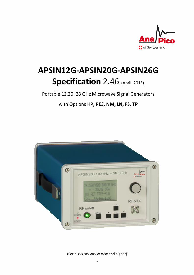
1 APSIN12G-APSIN20G-APSIN26G Specification 2.46 (April 2016) Portable 12,20, 28 GHz Microwave Signal Generators with Options HP, PE3, NM, LN, FS, TP (Serial xxx-xxxx8xxxx-xxxx and higher)
Transcript of APSIN12G-APSIN20G-APSIN26G Specification 2 · modulation and FM simulates Doppler effects or chirp...
1
APSIN12G-APSIN20G-APSIN26G
Specification 2.46 (April 2016)
Portable 12,20, 28 GHz Microwave Signal Generators
with Options HP, PE3, NM, LN, FS, TP
(Serial xxx-xxxx8xxxx-xxxx and higher)

2
Introduction
The APSINXXG is a series of low-noise and fast-switching microwave signal generators covering a
continuous frequency ranges from as low as 100 kHz up to 12, 20, and 26.5 GHz, respectively, with
a 0.001 Hz resolution.
The APSINXXG provide an accurately levelled output power range and high spurious suppression.
Advanced frequency synthesis with fractional-N divider makes for low SSB phase noise and micro-
Hz resolution.
Available Options:
Option HP delivers higher maximum output power to a level up to +27 dBm.
Option PE3 is an optional power level extension to accurately level below -90 dBm.
Option LN provides ultra low phase noise and further improves frequency stability
Option FS substantially reduces the switching speed
Option NM removes all built-in modulation capabilities if not needed (APSIN20G, APSIN26G only)
Option B3 adds an internal rechargeable battery module
Option 1URM modifies form-factor to a 19'' rack-mountable 1HU enclosure
Option TP modifies form-factor to a 3HU 19'' bench-top enclosre with touch-display control
The standard APSINXXG includes amplitude modulation (AM), DC-coupled, low distortion
wideband frequency modulation (FM), PM, FSK and PSK, frequency chirp, and fast pulse
modulation with internal pulse train generator. Three internal modulations sources are available.
All modulation modes of the APSINXXG can be combined. This allows the generation of complex
modulation signals for modern communication and location systems. The combination of pulse
modulation and FM simulates Doppler effects or chirp signals. Simultaneous AM and pulse
modulation provides the types of signal occurring in pulse radar applications with rotating
antenna. The combination of FM and AM can be used to check fading effects of FM receivers.
All APSINXXG allow fast analog and digital sweeps including flexible list sweeps, where frequency,
power and dwell times can be set individually. A flexible triggering capability simplifies
synchronization within test environments.
All APSINXXG operate with an ultra-stable temperature compensated 100 MHz reference (OCXO)
to ensure minimal drift, and can be phase-locked to any stable external reference in a range from
1 to 250 MHz. Additionally, optimum phase synchronous signals can be achieved by bypassing
internal and feeding a 100 MHz signal directly as reference.
The APSINXXG support various standard interfaces such as USB-TMC, LAN, and GPIB.
Applications for the APSINXXG include
• R&D low noise microwave source
• Production testing (industry-leading switching times; high dynamic range)
• Service and maintenance (battery operation)
• Signal simulation (Radar, WiMax, UWB)
• Aerospace & Defence (Pulse modulator, Chirps)
3
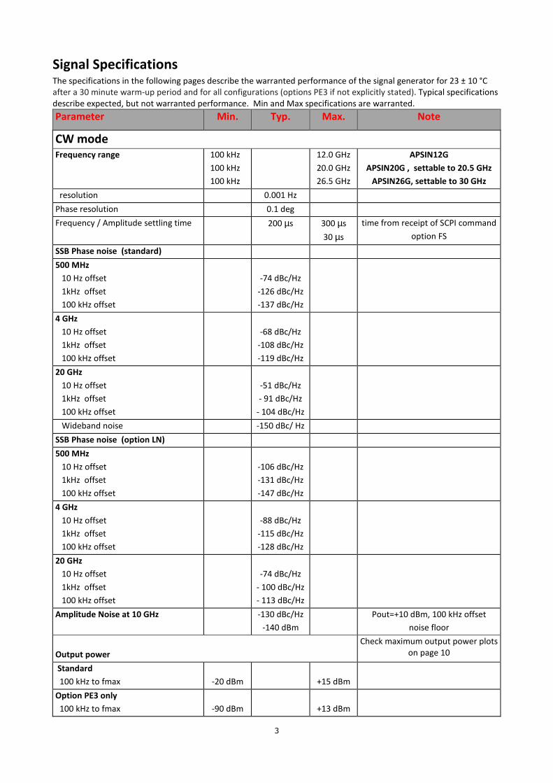
Signal Specifications The specifications in the following pages describe the warranted performance of the signal generator for 23 ± 10 °C
after a 30 minute warm-up period and for all configurations (options PE3 if not explicitly stated). Typical specifications
describe expected, but not warranted performance. Min and Max specifications are warranted.
Parameter Min. Typ. Max. Note
CW mode Frequency range 100 kHz
100 kHz
100 kHz
12.0 GHz
20.0 GHz
26.5 GHz
APSIN12G
APSIN20G , settable to 20.5 GHz
APSIN26G, settable to 30 GHz
resolution 0.001 Hz
Phase resolution 0.1 deg
Frequency / Amplitude settling time
200 µs
300 µs
30 µs
time from receipt of SCPI command
option FS
SSB Phase noise (standard)
500 MHz
10 Hz offset
1kHz offset
100 kHz offset
-74 dBc/Hz
-126 dBc/Hz
-137 dBc/Hz
4 GHz
10 Hz offset
1kHz offset
100 kHz offset
-68 dBc/Hz
-108 dBc/Hz
-119 dBc/Hz
20 GHz
10 Hz offset
1kHz offset
100 kHz offset
-51 dBc/Hz
- 91 dBc/Hz
- 104 dBc/Hz
Wideband noise -150 dBc/ Hz
SSB Phase noise (option LN)
500 MHz
10 Hz offset
1kHz offset
100 kHz offset
-106 dBc/Hz
-131 dBc/Hz
-147 dBc/Hz
4 GHz
10 Hz offset
1kHz offset
100 kHz offset
-88 dBc/Hz
-115 dBc/Hz
-128 dBc/Hz
20 GHz
10 Hz offset
1kHz offset
100 kHz offset
-74 dBc/Hz
- 100 dBc/Hz
- 113 dBc/Hz
Amplitude Noise at 10 GHz
-130 dBc/Hz
-140 dBm
Pout=+10 dBm, 100 kHz offset
noise floor
Output power
Check maximum output power plots
on page 10
Standard
100 kHz to fmax
-20 dBm
+15 dBm
Option PE3 only
100 kHz to fmax
-90 dBm
+13 dBm
4
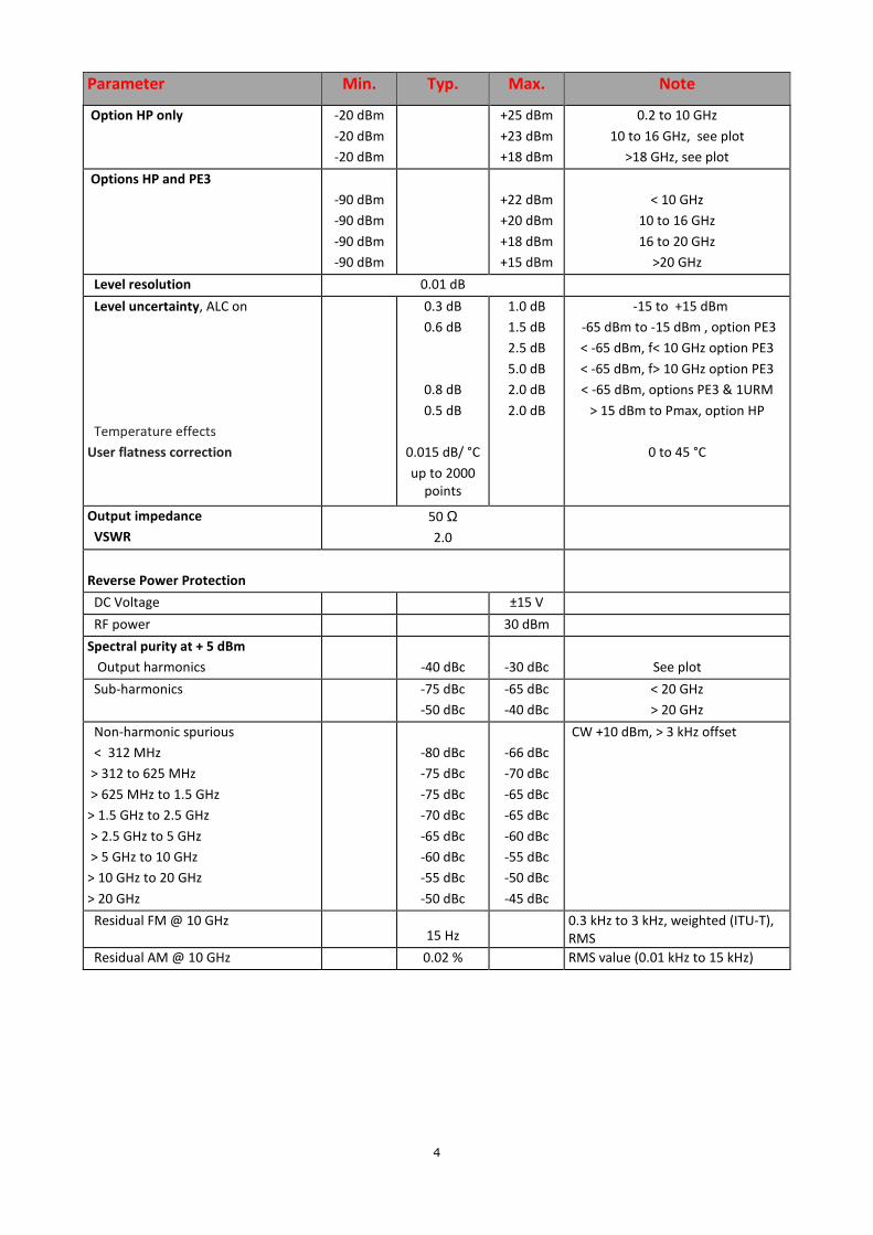
Parameter Min. Typ. Max. Note
Option HP only -20 dBm
-20 dBm
-20 dBm
+25 dBm
+23 dBm
+18 dBm
0.2 to 10 GHz
10 to 16 GHz, see plot
>18 GHz, see plot
Options HP and PE3
-90 dBm
-90 dBm
-90 dBm
-90 dBm
+22 dBm
+20 dBm
+18 dBm
+15 dBm
< 10 GHz
10 to 16 GHz
16 to 20 GHz
>20 GHz
Level resolution 0.01 dB
Level uncertainty, ALC on
Temperature effects
User flatness correction
0.3 dB
0.6 dB
0.8 dB
0.5 dB
0.015 dB/ °C
up to 2000
points
1.0 dB
1.5 dB
2.5 dB
5.0 dB
2.0 dB
2.0 dB
-15 to +15 dBm
-65 dBm to -15 dBm , option PE3
< -65 dBm, f< 10 GHz option PE3
< -65 dBm, f> 10 GHz option PE3
< -65 dBm, options PE3 & 1URM
> 15 dBm to Pmax, option HP
0 to 45 °C
Output impedance
VSWR
50 Ω
2.0
Reverse Power Protection
DC Voltage ±15 V
RF power 30 dBm
Spectral purity at + 5 dBm
Output harmonics
-40 dBc
-30 dBc
See plot
Sub-harmonics
-75 dBc
-50 dBc
-65 dBc
-40 dBc
< 20 GHz
> 20 GHz
Non-harmonic spurious
< 312 MHz
> 312 to 625 MHz
> 625 MHz to 1.5 GHz
> 1.5 GHz to 2.5 GHz
> 2.5 GHz to 5 GHz
> 5 GHz to 10 GHz
> 10 GHz to 20 GHz
> 20 GHz
-80 dBc
-75 dBc
-75 dBc
-70 dBc
-65 dBc
-60 dBc
-55 dBc
-50 dBc
-66 dBc
-70 dBc
-65 dBc
-65 dBc
-60 dBc
-55 dBc
-50 dBc
-45 dBc
CW +10 dBm, > 3 kHz offset
Residual FM @ 10 GHz 15 Hz
0.3 kHz to 3 kHz, weighted (ITU-T),
RMS
Residual AM @ 10 GHz 0.02 % RMS value (0.01 kHz to 15 kHz)

5
Sweeping Capability Sweeps can be performed with combined internal or external AM/FM/PM/pulse modulation running. With
modulation enabled, the minimum step time increases to 2 ms.
Parameter Min. Typ. Max. Note
Digital power / frequency / list sweeps Sweep type: linear, logarithmic, random
Step time (τstep)
400 µs
40 µs
19998 s
Option FS
Dwell time (τval) 10 µs 9999 s
Off-time (incl. transient time) (toff) 0 9999 s
Transient time (τinv) 270 µs
30 µs
Option FS
Timing delay (τde) 2 to 10 µs
50 ns
Option FS
Time resolution 0.1 µs
5 ns
Option FS
Timing accuracy per point 3 µs
5 ns
Option FS
Frequency Chirps (linear ramp, up/down)
Bandwidth 10 % of carrier frequency
Dwell time (tdwell) 10 ns 10000 µs
Slope 100 MHz /
µs
Number of frequencies 65’000

6
Reference Frequency REF IN input and REF OUT output are at rear panel
Parameter Min. Typ. Max. Note
Internal reference frequency 100 MHz
10 / 100 MHz
Option LN
Initial accuracy ±40 ppb calibrated at 23 ± 3 °C at time of
calibration , user adjustable
Temperature stability (0 to 50 degC) ±100 ppb
±20 ppb
Option LN
Aging 1st
year 0.5 ppm
0.1 ppm
Option LN
Aging per day (after 30days
operations)
5 ppb
tbm
Option LN
Warm-Up time 5 min
Output of internal reference
Output power
Output impedance
10 MHz
10/100 MHz
0 dBm
50 Ohms
Bypass Internal reference
Input
100 MHz, -5 to +10 dBm
100 MHz, 1 GHz
High phase synchronous mode
Option LN
Phase Lock to External Reference
External Input Range
1 MHz
250 MHz
User programmable
Reference input level -5 dBm 0 dBm +13 dBm
Lock Range ±1.5 ppm
Reference input impedance 50 Ohms
Multi Purpose Output (FUNC OUT) Output is FUNC OUT at rear panel
Parameter Min. Typ. Max. Note
MULTIFUNCTION GENERATOR sine, triangle, square wave
Frequency range 1 Hz
1 Hz
3 MHz
1 MHz
50 kHz
sine
triangle
square
Frequency resolution 0.1 Hz
Output voltage amplitude peak-peak 10 mV
5V
2 V Sine, triangle
Square (CMOS output)
Harmonic Distortion 1 % < 100 kHz, 1 Vpp
Output impedance 50 Ohms
CMOS
Sine, triangle
square wave
VIDEO OUTPUT (of internal pulse modulator)
Output CMOS
Period 30 ns 50 s
Pulse Width 15 ns 50 s
7
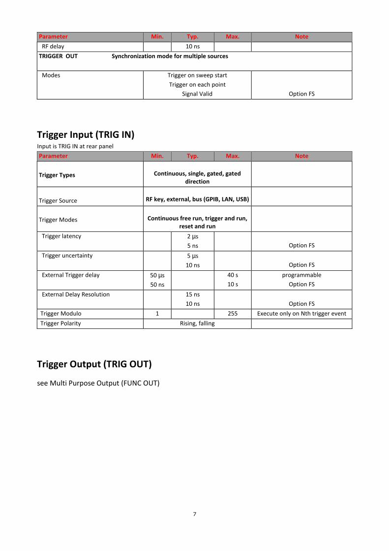
Parameter Min. Typ. Max. Note
RF delay 10 ns
TRIGGER OUT Synchronization mode for multiple sources
Modes Trigger on sweep start
Trigger on each point
Signal Valid
Option FS
Trigger Input (TRIG IN) Input is TRIG IN at rear panel
Parameter Min. Typ. Max. Note
Trigger Types Continuous, single, gated, gated
direction
Trigger Source RF key, external, bus (GPIB, LAN, USB)
Trigger Modes Continuous free run, trigger and run,
reset and run
Trigger latency 2 µs
5 ns
Option FS
Trigger uncertainty 5 µs
10 ns
Option FS
External Trigger delay 50 µs
50 ns
40 s
10 s
programmable
Option FS
External Delay Resolution 15 ns
10 ns
Option FS
Trigger Modulo 1 255 Execute only on Nth trigger event
Trigger Polarity Rising, falling
Trigger Output (TRIG OUT)
see Multi Purpose Output (FUNC OUT)

8
Modulation Capabilities (not with option NM) Combined AM/PM/FM/PULSE possible (see user manual)
Parameter Min. Typ. Max. Note
Multifunction Generator sine, triangle, square wave
Output is FUNC OUT at rear panel
Frequency range 1 Hz
1 Hz
3 MHz
1 MHz
50 kHz
sine
triangle
square
Frequency resolution 0.1 Hz
Output voltage amplitude peak-peak 10 mV
5V
2 V Sine, triangle
Square (CMOS output)
Harmonic Distortion 1 % < 100 kHz, 1 Vpp
Output impedance 50 Ohms
CMOS
Sine, triangle
square wave
Pulse Modulation On/off ratio
70 dB
at +10 dBm
Repetition frequency DC 10 MHz
Pulse width 30 ns
500 ns
ALC hold
ALC on
Pulse rise/fall time 7 ns
Pulse width 30 ns 100 µs
Pulse resolution 15 ns
Polarity selectable
External input amplitude 1 V
TTL
AC
DC
Pulse Pattern Modulation On/off ratio
70 dB
Using internal pattern generator
at +10 dBm
Pulse bit width 30 ns
500 ns
ALC hold
ALC on
Pulse rise/fall time 7 ns
Programmable pattern length 2 4192
Pulse width 30 ns 100 µs
Pulse bit resolution 15 ns
Polarity selectable
Frequency Modulation Maximum Frequency deviation
(peak)
> 0.05·f
N · 200 MHz
< 1.25 GHz
1.25 GHz to 2.5 GHz (N=0.125)
2.5 GHz to 5 GHz (N=0.25)
5 GHz to 10 GHz (N=0.5)
> 10 GHz to 20 GHz (N=1)
Deviation accuracy (1kHz rate, 50
kHz deviation) < 2%
Modulation rate DC 800 kHz > -3dB frequency response
Modulation waveforms Sine, triangle, FSK
External input sensitivity
AC
DC
0 to N · 200 MHz / V
0 to N · 100 MHz / V
adjustable for ±1 V range
discr. values ; ±5 V range
Total harmonic distortion < 1% 1 kHz rate & N · 1 MHz deviation

9
Parameter Min. Typ. Max. Note
Phase Modulation Phase deviation (peak) 0 N·300 rad
Modulation rate DC
800 kHz
> -3dB frequency response
Max. phase deviation degrades
above 20 kHz modulation rate
Modulation waveforms Sine, triangle, FSK
External Input sensitivity Settable 0.1 rad/V to 360 rad/V
Total harmonic distortion < 1% 1 kHz rate & N x 100 rad deviation
Amplitude Modulation
Modulation rate 0.1 Hz 50 kHz
Modulation waveforms Sine, triangle, square
Modulation depth 0 % 90 %
Distortion (sine wave) 2 % at 60% modulation depth
Accuracy (1kHz, 80%) - 4% 4 % for 10 to 80%, 0 dBm
Notes:

10
Typical performance curves
Phase Noise Performance (10 Hz to 50 MHz offset) at 1,4,13 and 26 GHz
Phase Noise with Option LN
11
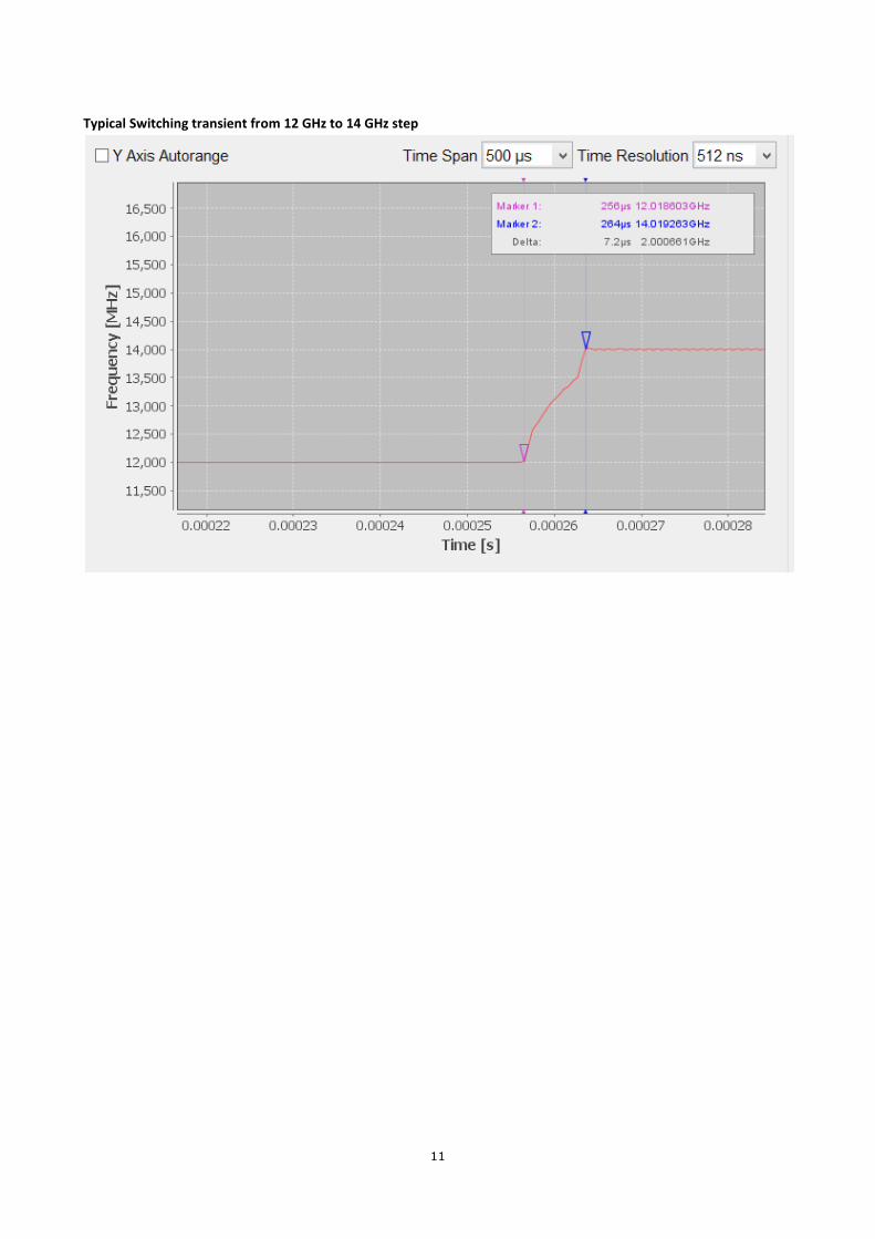
Typical Switching transient from 12 GHz to 14 GHz step

12
Typical Frequency Response 0 to 20 GHz at -20, 0, and +20 dBm
0.2 0.4 0.6 0.8 1 1.2 1.4 1.6 1.8 2
x 1010
-1.5
-1
-0.5
0
0.5
1
1.5
Frequency in Hz
Err
or in
dB
-20 dBm +0 dBm +20 dBm
-25 -20 -15 -10 -5 0 5 10 15 20-2
-1.5
-1
-0.5
0
0.5
1
1.5
2
Power set in dBm
ER
RO
R in
dB
5.0 GHz10.0 GHz15.0 GHz20.0 GHz

13
Typical Maximum Output Power (standard)
Typical Maximum Output Power (option HP)
0.2 0.4 0.6 0.8 1 1.2 1.4 1.6 1.8 2
x 1010
0
5
10
15
20
25
30
Frequency in Hz
Max
imu
m P
ow
er in
dB
m
0.5 1 1.5 2 2.5
x 1010
0
5
10
15
20
25
30
Frequency in Hz
Ou
tpu
t P
ow
er
in d
Bm
14
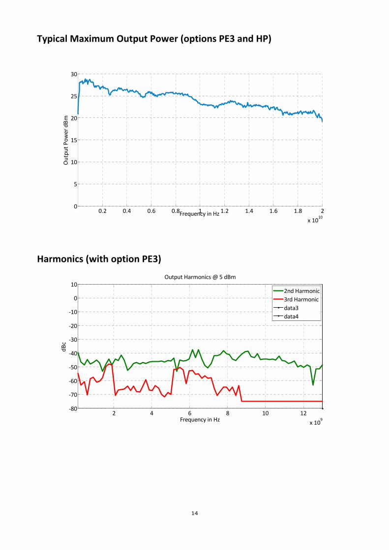
Typical Maximum Output Power (options PE3 and HP)
Harmonics (with option PE3)
0.2 0.4 0.6 0.8 1 1.2 1.4 1.6 1.8 2
x 1010
0
5
10
15
20
25
30
Frequency in Hz
Ou
tpu
t P
ow
er
dB
m
2 4 6 8 10 12
x 109
-80
-70
-60
-50
-40
-30
-20
-10
0
10
Output Harmonics @ 5 dBm
Frequency in Hz
dB
c
2nd Harmonic
3rd Harmonic
data3
data4

15
Connectors
Front panel:
1. RF output: SMA female
2. RF on/off button
3. Rotary knob
4. Menu and ↓ ↑ ← → arrow keys
Rear panel:
1. Trigger input: BNC female
2. Function output: BNC female
3. External reference input: BNC female
4. Internal reference output: BNC female
5. FM/PM modulation input: BNC female
6. AM and Pulse modulation: BNC female
7. LAN connection: RJ-45
8. USB 2.0 host and device
9. GPIB: IEEE-488.2, 1987 with listen and talk (optional)
10. DC Power plug (6V, 6A)
11. DC power switch

16
General Characteristics Remote programming interfaces
Ethernet 100BaseT LAN interface,
USB 2.0 host & device
GPIB (IEEE-488.2,1987) with listen and talk (optional)
Control language SCPI Version 1999.0
Power requirements 6.25 ± 0.2 VDC ; 20 W maximum
Mains adapter supplied: 100-240 VAC in/ 6 V 6.0 A DC out
Environmental (Levels similar to MIL-PRF-28800F Class 3/4)
Environmental stress Samples of this product have been type tested to be robust against the environmental stresses
of storage, transportation, and end-use; those stresses to temperature, humidity, shock, vibration, altitude, and
power line conditions.
Operating temperature range 0 to 40 °C
Storage temperature range –40 to 70 °C
Operating and storage altitude up to 15,000 feet (4600 m)
notice
Safety/EMC complies with applicable Safety and EMC regulations and directives.
Weight ≤ 2.5 kg (6 lbs) net, ≤ 4 kg (8 lb.) shipping
Dimensions 106 mm H x 172 mm W x 270 mm L (incl. connectors)
[4.21 in H x 6.77 in W x 10.63 in L]
Recommended calibration cycle 24 months
Options • HP: High output power
• PE3: Extended power range down to <-90 dBm) step attenuator module
• NM: remove modulation
• LN: ultra low phase noise, improved frequency stability
• FS: enhanced switching speed
• B3: battery module
• TP: 3HE enclosure with touch display. Dimensions incl. rubber: 154 mm H x 467.5 mm W x 342 mm L [6.1 in H
x 18.4 in W x 13.5 in L]
• GPIB: IEEE-488.2,1987 programming interface

17
• 1URM: 19'' 1HE enclosure with rack-mount capability. Dimensions 42 mm H x 426 mm W x 460 mm L [1.7 in
H x 16.8 in W x 18.1 in L]
• GPIB: IEEE-488.2,1987 programming interface
• RM: 19’’ rackmount kit: good for one or two adjacent APSIN
Document History Version/Status Date Author Notes
V10 2010-06-01 jk first release
V11 2010-08-30 jk added specs for VSWR, AM noise, residual
V13 2010-10-15 jk power, frequency range, modulation specs updated
V14 2011-04-28 jk Frequency and power range , Output connector, added phase
noise plot
V160 2013-08-26 db Modified sweep timing specs, added max power measurement
plots
V20 2014-07-30 jk Combined APSIN20G and option HP
V21 2014-11-10 jk Added pulse pattern specs
V22 2014-12-10 jk Unified data sheet for APSINXXG
V23 2015-1-15 jk Addeded max. power plots
V240 2015-10-29 jk Clarified switching speed, Phase noise revised
V241 2015-12-18 jk Power level accuracy refined
V241 2016_01-12 jk Refined spurous specs
V245 2016_03-04 jk Included ALC temp effects, renewed phase noise plots
V246 2016_04-04 jk Power level accuracy option deppendant


