Application of the Texas Instruments AUC Sub-1-V Little Logic
32
Application Report SCEA027A - September 2002 1 Application of the Texas Instruments AUC Sub-1-V Little Logic Devices Chris Maxwell and Tomdio Nana Standard Linear & Logic ABSTRACT Power consumption and speed are always concerns in electronic system logic design. Texas Instruments (TI) announces the industry’s first sub-1-V logic family that provides significant benefits to portable consumer electronics by operating at low power and high speed, while maintaining overall system signal integrity. TI’s next-generation logic family is the advanced ultra-low-voltage CMOS (AUC) family. Although optimized for 1.8-V operation, AUC logic supports mixed-voltage systems because it is compatible with 0.8-V, 1.2-V, 1.5-V and 2.5-V devices. The AUC logic inputs tolerate 3.6-V signals, thus enabling level-translation down from 3.3-V nodes to lower-voltage nodes. Further, AUC logic has the I off feature, which supports the partial-power-down mode of operation. This application report discusses AUC Little Logic device features, characteristics, and applications. Keywords: 0.8 V, 1.2 V, 1.5 V, 1.8 V, 2.5 V, 3.3-V tolerant, AUC, electrical performance, I off , level translation, Little Logic, open drain, overvoltage protection, partial power down, signal integrity, ULTTL Contents 1 Introduction 4 . . . . . . . . . . . . . . . . . . . . . . . . . . . . . . . . . . . . . . . . . . . . . . . . . . . . . . . . . . . . . . . . . . . . . . . . . 2 AUC Little Logic Features 4 . . . . . . . . . . . . . . . . . . . . . . . . . . . . . . . . . . . . . . . . . . . . . . . . . . . . . . . . . . . . 2.1 Novel Output Structure 4 . . . . . . . . . . . . . . . . . . . . . . . . . . . . . . . . . . . . . . . . . . . . . . . . . . . . . . . . . . . . 2.2 Level-Translation Support 6 . . . . . . . . . . . . . . . . . . . . . . . . . . . . . . . . . . . . . . . . . . . . . . . . . . . . . . . . . 2.3 Power-Off Support 7 . . . . . . . . . . . . . . . . . . . . . . . . . . . . . . . . . . . . . . . . . . . . . . . . . . . . . . . . . . . . . . . . 3 AUC Little Logic Device Characteristics 7 . . . . . . . . . . . . . . . . . . . . . . . . . . . . . . . . . . . . . . . . . . . . . . . 3.1 Input Characteristics 7 . . . . . . . . . . . . . . . . . . . . . . . . . . . . . . . . . . . . . . . . . . . . . . . . . . . . . . . . . . . . . . 3.1.1 Input Capacitance 7 . . . . . . . . . . . . . . . . . . . . . . . . . . . . . . . . . . . . . . . . . . . . . . . . . . . . . . . . . . 3.1.2 Input Voltage Tolerance 7 . . . . . . . . . . . . . . . . . . . . . . . . . . . . . . . . . . . . . . . . . . . . . . . . . . . . . 3.1.3 Slow-Input-Edge-Rate Compatibility 8 . . . . . . . . . . . . . . . . . . . . . . . . . . . . . . . . . . . . . . . . . . 3.2 Electrical Characteristics 11 . . . . . . . . . . . . . . . . . . . . . . . . . . . . . . . . . . . . . . . . . . . . . . . . . . . . . . . . . 3.2.1 AC Performance 11 . . . . . . . . . . . . . . . . . . . . . . . . . . . . . . . . . . . . . . . . . . . . . . . . . . . . . . . . . . 3.2.2 DC Performance 13 . . . . . . . . . . . . . . . . . . . . . . . . . . . . . . . . . . . . . . . . . . . . . . . . . . . . . . . . . . 3.3 Power Consumption 14 . . . . . . . . . . . . . . . . . . . . . . . . . . . . . . . . . . . . . . . . . . . . . . . . . . . . . . . . . . . . . 4 Design Issues and AUC Little Logic Solutions 16 . . . . . . . . . . . . . . . . . . . . . . . . . . . . . . . . . . . . . . . . 4.1 Signal Integrity 16 . . . . . . . . . . . . . . . . . . . . . . . . . . . . . . . . . . . . . . . . . . . . . . . . . . . . . . . . . . . . . . . . . . 4.2 Mixed-Voltage-Mode Data Communication 19 . . . . . . . . . . . . . . . . . . . . . . . . . . . . . . . . . . . . . . . . . . 4.3 Partial Power Down 20 . . . . . . . . . . . . . . . . . . . . . . . . . . . . . . . . . . . . . . . . . . . . . . . . . . . . . . . . . . . . . . 4.4 Low Power Consumption 21 . . . . . . . . . . . . . . . . . . . . . . . . . . . . . . . . . . . . . . . . . . . . . . . . . . . . . . . . . TI and Widebus are trademarks of Texas Instruments.
Transcript of Application of the Texas Instruments AUC Sub-1-V Little Logic

Application ReportSCEA027A - September 2002
1
Application of the Texas InstrumentsAUC Sub-1-V Little Logic Devices
Chris Maxwell and Tomdio Nana Standard Linear & Logic
ABSTRACT
Power consumption and speed are always concerns in electronic system logic design. TexasInstruments (TI) announces the industry’s first sub-1-V logic family that provides significantbenefits to portable consumer electronics by operating at low power and high speed, whilemaintaining overall system signal integrity. TI’s next-generation logic family is the advancedultra-low-voltage CMOS (AUC) family. Although optimized for 1.8-V operation, AUC logicsupports mixed-voltage systems because it is compatible with 0.8-V, 1.2-V, 1.5-V and 2.5-Vdevices. The AUC logic inputs tolerate 3.6-V signals, thus enabling level-translation downfrom 3.3-V nodes to lower-voltage nodes. Further, AUC logic has the Ioff feature, whichsupports the partial-power-down mode of operation. This application report discusses AUCLittle Logic device features, characteristics, and applications.
Keywords: 0.8 V, 1.2 V, 1.5 V, 1.8 V, 2.5 V, 3.3-V tolerant, AUC, electrical performance, Ioff,level translation, Little Logic, open drain, overvoltage protection, partial power down, signalintegrity, ULTTL
Contents
1 Introduction 4. . . . . . . . . . . . . . . . . . . . . . . . . . . . . . . . . . . . . . . . . . . . . . . . . . . . . . . . . . . . . . . . . . . . . . . . .
2 AUC Little Logic Features 4. . . . . . . . . . . . . . . . . . . . . . . . . . . . . . . . . . . . . . . . . . . . . . . . . . . . . . . . . . . . 2.1 Novel Output Structure 4. . . . . . . . . . . . . . . . . . . . . . . . . . . . . . . . . . . . . . . . . . . . . . . . . . . . . . . . . . . . 2.2 Level-Translation Support 6. . . . . . . . . . . . . . . . . . . . . . . . . . . . . . . . . . . . . . . . . . . . . . . . . . . . . . . . . 2.3 Power-Off Support 7. . . . . . . . . . . . . . . . . . . . . . . . . . . . . . . . . . . . . . . . . . . . . . . . . . . . . . . . . . . . . . . .
3 AUC Little Logic Device Characteristics 7. . . . . . . . . . . . . . . . . . . . . . . . . . . . . . . . . . . . . . . . . . . . . . . 3.1 Input Characteristics 7. . . . . . . . . . . . . . . . . . . . . . . . . . . . . . . . . . . . . . . . . . . . . . . . . . . . . . . . . . . . . .
3.1.1 Input Capacitance 7. . . . . . . . . . . . . . . . . . . . . . . . . . . . . . . . . . . . . . . . . . . . . . . . . . . . . . . . . . 3.1.2 Input Voltage Tolerance 7. . . . . . . . . . . . . . . . . . . . . . . . . . . . . . . . . . . . . . . . . . . . . . . . . . . . . 3.1.3 Slow-Input-Edge-Rate Compatibility 8. . . . . . . . . . . . . . . . . . . . . . . . . . . . . . . . . . . . . . . . . .
3.2 Electrical Characteristics 11. . . . . . . . . . . . . . . . . . . . . . . . . . . . . . . . . . . . . . . . . . . . . . . . . . . . . . . . . 3.2.1 AC Performance 11. . . . . . . . . . . . . . . . . . . . . . . . . . . . . . . . . . . . . . . . . . . . . . . . . . . . . . . . . . 3.2.2 DC Performance 13. . . . . . . . . . . . . . . . . . . . . . . . . . . . . . . . . . . . . . . . . . . . . . . . . . . . . . . . . .
3.3 Power Consumption 14. . . . . . . . . . . . . . . . . . . . . . . . . . . . . . . . . . . . . . . . . . . . . . . . . . . . . . . . . . . . .
4 Design Issues and AUC Little Logic Solutions 16. . . . . . . . . . . . . . . . . . . . . . . . . . . . . . . . . . . . . . . . 4.1 Signal Integrity 16. . . . . . . . . . . . . . . . . . . . . . . . . . . . . . . . . . . . . . . . . . . . . . . . . . . . . . . . . . . . . . . . . . 4.2 Mixed-Voltage-Mode Data Communication 19. . . . . . . . . . . . . . . . . . . . . . . . . . . . . . . . . . . . . . . . . . 4.3 Partial Power Down 20. . . . . . . . . . . . . . . . . . . . . . . . . . . . . . . . . . . . . . . . . . . . . . . . . . . . . . . . . . . . . . 4.4 Low Power Consumption 21. . . . . . . . . . . . . . . . . . . . . . . . . . . . . . . . . . . . . . . . . . . . . . . . . . . . . . . . .
TI and Widebus are trademarks of Texas Instruments.
SCEA027A
2 Application of the Texas Instruments AUC Sub-1-V Little Logic Devices
5 Package Information 22. . . . . . . . . . . . . . . . . . . . . . . . . . . . . . . . . . . . . . . . . . . . . . . . . . . . . . . . . . . . . . . .
6 Features and Benefits 23. . . . . . . . . . . . . . . . . . . . . . . . . . . . . . . . . . . . . . . . . . . . . . . . . . . . . . . . . . . . . . .
7 Conclusion 23. . . . . . . . . . . . . . . . . . . . . . . . . . . . . . . . . . . . . . . . . . . . . . . . . . . . . . . . . . . . . . . . . . . . . . . . .
8 Frequently Asked Questions (FAQs) 23. . . . . . . . . . . . . . . . . . . . . . . . . . . . . . . . . . . . . . . . . . . . . . . . .
9 References 25. . . . . . . . . . . . . . . . . . . . . . . . . . . . . . . . . . . . . . . . . . . . . . . . . . . . . . . . . . . . . . . . . . . . . . . . .
10 Glossary 25. . . . . . . . . . . . . . . . . . . . . . . . . . . . . . . . . . . . . . . . . . . . . . . . . . . . . . . . . . . . . . . . . . . . . . . . . . .
Appendix A. Parameter Measurement Information 27. . . . . . . . . . . . . . . . . . . . . . . . . . . . . . . . . . . . . . . . .
Appendix B. Mechanical Data 29. . . . . . . . . . . . . . . . . . . . . . . . . . . . . . . . . . . . . . . . . . . . . . . . . . . . . . . . . . . .
List of Figures
1. ULTTL Output Structure 5. . . . . . . . . . . . . . . . . . . . . . . . . . . . . . . . . . . . . . . . . . . . . . . . . . . . . . . . . . . . . 2. Output Drive Currents of UOP During Low-to-High Transition 6. . . . . . . . . . . . . . . . . . . . . . . . . . . . . 3. SN74AUC1G00 Slow-Input Transition-Time Plot, ∆t/∆V = 11.69 ns/V 9. . . . . . . . . . . . . . . . . . . . . . 4. SN74AUC1G00 Slow-Input Transition-Time Plot, ∆t/∆V = 23.19 ns/V 10. . . . . . . . . . . . . . . . . . . . . 5. tpd vs Capacitive Load at 2.5-V, 1.8-V, and 1.5-V VCC 12. . . . . . . . . . . . . . . . . . . . . . . . . . . . . . . . . . 6. tpd vs Capacitive Load at 1.2-V and 0.8-V VCC 12. . . . . . . . . . . . . . . . . . . . . . . . . . . . . . . . . . . . . . . . 7. VOH vs IOH for AUC1G Devices 13. . . . . . . . . . . . . . . . . . . . . . . . . . . . . . . . . . . . . . . . . . . . . . . . . . . . . 8. VOL vs IOL for AUC1G Devices 14. . . . . . . . . . . . . . . . . . . . . . . . . . . . . . . . . . . . . . . . . . . . . . . . . . . . . . 9. Relative Power Efficiency of Selected Little Logic Devices 15. . . . . . . . . . . . . . . . . . . . . . . . . . . . . . . 10. Transmission-Line Test Points for Simulations 16. . . . . . . . . . . . . . . . . . . . . . . . . . . . . . . . . . . . . . . . . 11. Output Impedance, Output Voltage, and Receiver Voltage of AUC Single-Gate
Transmission-Line Simulation 17. . . . . . . . . . . . . . . . . . . . . . . . . . . . . . . . . . . . . . . . . . . . . . . . . . . . . . . 12. Simulation of 65-Ω Transmission Line Across Supply Voltage and Temperature 17. . . . . . . . . . . . 13. Simulation of Low-to-High Transition into 30-Ω to 70-Ω Transmission Line 18. . . . . . . . . . . . . . . . . 14. Simulation of High-to-Low Transition into 30-Ω to 70-Ω Transmission Line 18. . . . . . . . . . . . . . . . . 15. Device at 1.8-V VCC, With 2.5-V or 3.3-V Inputs, Showing Switching Levels 19. . . . . . . . . . . . . . . 16. Circuit for Voltage Translation Using the SN74AUC1G07 20. . . . . . . . . . . . . . . . . . . . . . . . . . . . . . . . 17. ICC vs Frequency for Different AUC Little Logic Devices 21. . . . . . . . . . . . . . . . . . . . . . . . . . . . . . . . 18. ICC vs Frequency for SN74AUC1G06 and SN74LVC1G06 Devices 22. . . . . . . . . . . . . . . . . . . . . . 19. AUC Little Logic (with ULTTL Outputs) Load Circuit and Voltage Waveforms 27. . . . . . . . . . . . . . . 20. AUC Little Logic (with Open-Drain Outputs) Load Circuit and Voltage Waveforms 28. . . . . . . . . . 21. Plastic Small Outline Package (DBV) 29. . . . . . . . . . . . . . . . . . . . . . . . . . . . . . . . . . . . . . . . . . . . . . . . . 22. Plastic Small Outline Package (DCK) 30. . . . . . . . . . . . . . . . . . . . . . . . . . . . . . . . . . . . . . . . . . . . . . . . . 23. Die-Size Ball Grid Array (YEA or YZA) 31. . . . . . . . . . . . . . . . . . . . . . . . . . . . . . . . . . . . . . . . . . . . . . . .

SCEA027A
3 Application of the Texas Instruments AUC Sub-1-V Little Logic Devices
List of Tables
1. Input Capacitance and Speed Comparison for Comparable Families 7. . . . . . . . . . . . . . . . . . . . . . 2. Input Transition for Some AUC Little Logic Devices 10. . . . . . . . . . . . . . . . . . . . . . . . . . . . . . . . . . . . 3. Timing Characteristics of AUC Little Logic Devices 11. . . . . . . . . . . . . . . . . . . . . . . . . . . . . . . . . . . . . 4. Power Consumption and Speed of Selected Little Logic Devices at Their
Optimized Supply-Voltage Nodes 15. . . . . . . . . . . . . . . . . . . . . . . . . . . . . . . . . . . . . . . . . . . . . . . . . . . . 5. Requirements for Voltage Translation Between Devices A and B 20. . . . . . . . . . . . . . . . . . . . . . . . . 6. Features and Benefits of AUC Little Logic Devices 23. . . . . . . . . . . . . . . . . . . . . . . . . . . . . . . . . . . . .

SCEA027A
4 Application of the Texas Instruments AUC Sub-1-V Little Logic Devices
1 IntroductionMany electronic applications have shifted from the legacy bipolar TTL interface to CMOSrail-to-rail interface. The CMOS technology has facilitated supply-voltage migration from 5 V to3.3 V, 2.5 V, 1.8 V, 1.5 V, 1.2 V, and 0.8 V. These lower-voltage nodes allow decreased powerconsumption in the system. To facilitate migration to lower-voltage nodes, TI has released theadvanced ultra-low-voltage CMOS (AUC) family, which is optimized for 1.8-V operation and iscompatible with 0.8-V, 1.2-V, 1.5-V, 1.8-V, and 2.5-V devices.
TI offers the AUC functions in Widebus , octal, gates, and Little Logic (single, double, and triplegate) options. The widebus, octal, and gate AUC devices are designed for high-speed datathroughput and enhanced signal integrity to target bus applications in telecommunications andcomputing systems. The Little Logic AUC devices have high speed, low power consumption,and low-noise characteristics, which make them suitable for portable consumer electronicsapplications.
This application report discusses AUC Little Logic device features, characteristics, andapplications.
2 AUC Little Logic FeaturesThe AUC Little Logic devices are designed for use in battery-operated portable consumerelectronics or to fix design bugs in electronic systems. The characteristic output structure,level-translation support capability, and partial-power-down support features of the AUC LittleLogic facilitate the use of these devices in their targeted applications.
2.1 Novel Output Structure
The AUC Little Logic features the ultra-low-voltage transistor-transistor logic (ULTTL) outputdriver. The ULTTL is a new CMOS-technology interface driver designed for applicationsrequiring high-speed, low power consumption, and optimal signal integrity, while maintaining thebipolar TTL output characteristic of reduced line-reflection noise. With the migration from bipolarTTL technology to CMOS technology for lower-operating-voltage nodes, the ULTTL output driverwas developed to minimize switching noise, which is inherent in high-speed applications.
The ULTTL output driver of the AUC Little Logic changes impedance during transition. Threebasic output features are critical for optimal performance in low-voltage high-speed applications.First, the device must provide low-impedance (i.e., high dynamic current) drive during the initialphase of the transition through the ac threshold (i.e., VCC/2). This initial high drive provides thequick transition to the desired logic level and ensures that system timing is preserved. During thesecond phase of the transition, the impedance must be equal to that of the transmission-linemedium it is driving, to minimize ringing and optimize signal integrity. A major cause of ringing inpoint-to-point applications is the result of a mismatch or discontinuity between the outputimpedance of the driver and the impedance of the transmission line (i.e., PCB trace). AUC LittleLogic devices have been optimized for transmission lines of 50 Ω to 65 Ω, which is typical ofmost portable PCB applications. Finally, the output should stabilize at an impedance low enoughto provide the required dc drive. For most portable applications, 4-mA dc drive is sufficient;however, for nonportable applications, more drive current might be required.
The majority of application loads targeted for the AUC Little Logic family can be represented asa transmission line rather than a dc load. Thus, ac operation is dominated by the inductance andcapacitance of the load and, in most cases, heavy drive capabilities are not required, althoughthey are provided up to 8 mA at 1.8-V VCC.

SCEA027A
5 Application of the Texas Instruments AUC Sub-1-V Little Logic Devices
AUC Little Logic devices provide 8-mA dc drive current at the 1.8-V VCC node for nonportableapplications, while maintaining the signal-integrity performance of a 4-mA dc driver. The ULTTLoutput used in the AUC Little Logic family is designed to address each of the three criticalperformance requirements previously noted. Figure 1 shows a schematic of the ULTTL outputstructure.
DCB
VOUT
TLBACB
ControlFeedback
ControlFeedback
InternalNode
Figure 1. ULTTL Output Structure
To achieve the three impedance phases, the ULTTL output utilizes a three-branch p-channelupper-output (UOP) and three-branch n-channel lower-output (LOP) structure (see Figure 1).For the purpose of illustration, the three branches are referred to in this application report as theac branch (ACB), the transmission-line branch (TLB), and the dc branch (DCB). The first branch,which uses the diode in the output structure, provides the high dynamic current required to drivethrough the ac threshold. The second branch, which contains a series resistor, providesoptimized impedance matching into the transmission line. The third branch provides theadditional dc current drive for applications requiring more than 4 mA of output drive current at1.8-V VCC.
Each independent branch posses a unique on-state resistance (ron). As the output transitionsfrom a low to high (or high to low), the equivalent resistance of all branches varies in a controlledmanner by adjusting the individual resistance of each branch. The low-to-high transitionfunctions similarly to the high-to-low transition. The output impedance is controlled during thelow-to-high transition sequential action outlined below and shown in Figure 2.
1. During the initial phase of the transition, all three legs are turned on. The parallel ron of allthree legs provides very low combined impedance.
2. During the second phase of the transition, the ACB and DCB are turned off, and theoutput transitions to a higher impedance. As the output voltage level approaches VCC, theseries diode begins to saturate and, eventually, becomes reverse biased, causing thecurrent through the ACB to be reduced to less than 1 mA (basically, turned off). Athreshold-controlled feedback circuit turns off the DCB. The thresholds are adjusted, tominimize the effect of oscillations directly at the output of the driver before entering thetransmission line. (NOTE: A major advantage for the DCB being turned on in the initialstage is to provide support for the ACB at lower VCC ranges where speed often issacrificed.) The TLB ron is 50 Ω to 65 Ω and, because it is the last branch remaining on, itprovides the impedance matching to the transmission line.

SCEA027A
6 Application of the Texas Instruments AUC Sub-1-V Little Logic Devices
3. In the final phase of the transition, the DCB is turned on by the threshold-controlledfeedback circuit to provide a combined DCB and TLB equivalent resistance that issatisfactory for driving applications requiring more than 4 mA of output drive current at1.8-V VCC.
Time – ns
DCB
ACB
TLB
VOUT
0
–5
–10
–15
–20
–25
211 212 213 214 215 216 217 218 219 220
Cu
rren
t –
mA
V
–
VO
UT
2.0
1.8
1.6
1.4
1.2
1.0
0.8
0.6
0.4
0.2
0.0
–0.2
VCC = 1.8 VTJ = 25°CNominal Process
Stg 1 Stg 2 Stg 3
Figure 2. Output Drive Current of UOP During Low-to-High Transition
2.2 Level-Translation Support
Because the AUC Little Logic family uses a 0.8-V to 2.5-V power supply, interfacing AUC LittleLogic devices with other components that use a 3.3-V power supply becomes a concern. If anAUC Little Logic device is subjected to 3.3-V at its inputs, it is critical that the device not bedamaged. The term 3.3-V tolerance implies that the presence of 3.3-V at either the input or theoutput of the AUC device will not damage it. This feature enables AUC Little Logic devices to beused for level-translation support from higher-voltage nodes to lower-voltage nodes within the0.8-V and 3.3-V nodes.
Whether a device can tolerate 3.3-V only at the input, only at the output, or at both the input andoutput must be considered. Every AUC Little Logic device TI produces can be subjected to 3.3-Vat its input and not be damaged. Thus, all TI AUC Little Logic devices are 3.3-V input tolerant.
Whether or not an AUC Little Logic device can be subjected to 3.3-V at its output requiresconsideration. For the term 3.3-V output tolerant to be meaningful, the outputs of the devicemust be capable of being placed in the high-impedance state. Only the SN74AUC1G06,SN74AUC1G07, SN74AUC1G125, SN74AUC1G126, and SN74AUC1G240 havehigh-impedance outputs, and it is to these devices only that the term 3.3-V output tolerantapplies. For those devices with outputs capable of being placed in the high-impedance state,3.3-V output tolerance means that 3.3 V at its output does not damage the device.

SCEA027A
7 Application of the Texas Instruments AUC Sub-1-V Little Logic Devices
The AUC Little Logic functions that do not have high-impedance-state outputs should not beconnected to 3.3-V. This means that 3.3-V output tolerance does not make sense for thesedevices because their outputs cannot be placed in the high-impedance state.
2.3 Power-Off Support
The inputs and outputs of the AUC family have a blocking diode in the reversed-current paths toVCC. In this configuration, the maximum leakage current into or out of the input or outputtransistors is negligible when forcing the input or output to 3.3 V and VCC = 0 V. This off-stateleakage current (Ioff) is small enough to allow the device to remain electrically connected to abus during partial power down without loading the remaining live circuits. This feature alsoallows the use of this family in a mixed-voltage environment.
3 AUC Little Logic Device Characteristics
3.1 Input Characteristics
3.1.1 Input Capacitance
The AUC Little Logic devices provide a low input capacitance-to-speed ratio relative to similarproducts (see Table 1). Two major design factors influence input capacitance: speed andcapacitive-load-driving requirements. As speed requirements become more critical, the numberof internal stages for a given integrated circuit must be reduced to minimize propagation delay.In addition to a reduction in stages, unless the requirement to drive large capacitive loads isreduced (especially for nonportable applications), the output stage must be large enough todrive these loads. In most cases, the combination of these two factors results in a higher inputcapacitance because the large input capacitance of the output stage is transferred to the inputstage. Simply placing a small (low input capacitance) input stage in front of the large outputstage does not result in less propagation delay.
Table 1. Input Capacitance and Speed Comparison for Comparable Families
Device Input Capacitance(pF)
tpd at 1.8-V VCC(ns)
SN74AUC1G00 3.0 2.5
SN74LVC1G00 4.0 8.0
SN74ALVC00 4.5 4.4
The AUC Little Logic devices can maintain a comparable low input capacitance of 3 pF (typical),while providing high dynamic drive capability for larger loads and providing a propagation delayless than 2.5 ns at 1.8-V VCC (see Table 1).
3.1.2 Input Voltage Tolerance
As previously mentioned, AUC Little Logic devices operate with a 0.8-V to 2.7-V VCC. Therefore,interfacing AUC Little Logic with other components that use 3.3-V VCC might be a concern. Insuch systems, AUC Little Logic devices must have tolerance for input levels up to andexceeding 3.3 V, as well as below 0 V, without causing damage to the inputs. The AUC LittleLogic devices allow input voltages to exceed 3.3 V, up to 3.6 V, to allow extra protection for thefollowing reasons:

SCEA027A
8 Application of the Texas Instruments AUC Sub-1-V Little Logic Devices
• The 3.3-V system power supply might not stabilize at 3.3 V, but reach 3.6 V. Consequently,the output of the device driving the AUC Little Logic device could reach 3.6 V as well.
• The 3.3-V system power supply may stabilize at 3.3 V, but overshoots and undershoots cancause the input voltage into the AUC Little Logic devices to exceed the 0-V to 3.3-V range.
The AUC Little Logic devices support input voltages up to 3.6 V and must be operated within thefollowing guidelines:
• The recommended operating conditions specified in the data sheets restrict the input voltageto 0 V to 3.6 V, while the absolute maximum ratings specify the input voltage to be –0.5 V to4.1 V. As the data sheet indicates, stresses beyond those listed under absolute maximumratings may cause permanent damage to the device. The absolute maximum ratings arestress ratings only, and functional operation of the device at those or any other conditionsbeyond those indicated under recommended operating conditions is not implied. Exposure toabsolute-maximum-rated conditions may affect device reliability.
• Because the input-voltage range is limited from 0 V to 3.6 V, for 3.3-V systems, propertermination must be used on the inputs of AUC Little Logic devices to ensure that overshootdoes not exceed 3.6 V.
3.1.3 Slow-Input-Edge-Rate Compatibility
The AUC Little Logic devices are designed and tested for high-speed systems (i.e., systemsrequiring a fast input edge rate) with input transition signals less than 1 ns/V. However, theremay be several applications where it is desired to operate the device at a low frequency. In suchapplications, an input edge rate greater than 1 ns/V might be required. AUC Little Logic devicessupport such low-frequency applications.
A slow-input test sheds light on the integrity of the device, specifically, how the device respondswhen the input voltage is slowly ramped from 0 V to VCC and, conversely, when the input voltageis ramped slowly from VCC to 0 V. As the input voltage is ramping, the output voltage ismonitored and, when it begins to switch, the waveform is observed. If nonmonotonic behavior isobserved as the output traverses the threshold region, the device may be sensitive to a slowinput, which can cause the output to oscillate or cause false triggering.
Figure 3 shows a passing case of slow-input-transition-rate tests. The test was done in thelaboratory using the SN74AUC1G00 with VCC = 2.7 V and the device at –40°C, with both inputstied together for the worst-case condition. In Figure 3, the input transition rate is fast enough(11.69 ns/V) to not cause any oscillation at the output.

SCEA027A
9 Application of the Texas Instruments AUC Sub-1-V Little Logic Devices
100900 10 20 30 40 50 60 70 80
Time – ns
3.5
3.0
2.5
2.0
1.5
1
0.5
0
–0.5
Input
OutputV
olt
age
– V
Figure 3. SN74AUC1G00 Slow-Input-Transition-Time Plot, ∆t/∆V = 11.69 ns/V
Figure 4 shows a failure case of slow-input-transition-rate tests. The test was done in thelaboratory using the SN74AUC1G00 with VCC = 2.7 V and the device at –40°C, with both inputstied together for the worst-case condition. In Figure 4, the input transition rate is too slow(23.19 ns/V) and causes oscillations at the output.

SCEA027A
10 Application of the Texas Instruments AUC Sub-1-V Little Logic Devices
100900 10 20 30 40 50 60 70 80
Time – ns
3.5
3.0
2.5
2.0
1.5
1
0.5
0
–0.5
Input
OutputV
olt
age
– V
Figure 4. SN74AUC1G00 Slow-Input-Transition-Time Plot, ∆t/∆V = 23.19 ns/V
Table 2 shows the maximum input transition rise or fall rate for some AUC Little Logic devices atdifferent voltage nodes. At the optimized voltage node, all AUC Little Logic devices shownoncritical responses to the slow-input test.
Table 2. Input Transition for Some AUC Little Logic Devices
Device
Maximum Input Transition Rise or Fall Rate, ∆t/∆V(ns/V)
VCC = 0.8 V VCC = 1.3 V VCC = 1.6 V VCC = 1.95 V VCC = 2.7 V
SN74AUC1G00 20 20 20 20 10
SN74AUC1G04 20 20 20 20 5
SN74AUC1G07 20 20 20 20 15
SN74AUC1G14 20 20 20 20 20
SN74AUC1G17 20 20 20 20 20
SN74AUC1G32 20 20 20 20 20
Table 2 shows that the AUC Little Logic devices can operate with slow signals (∆t/∆V > 1 ns/V)at the inputs. However, power consumption increases significantly with increased input transitionrise or fall rates.

SCEA027A
11 Application of the Texas Instruments AUC Sub-1-V Little Logic Devices
3.2 Electrical Characteristics
In most electronic-system applications, it is important for the integrated circuit drivers to providebalanced high and low drive during ac transition, which ensures balanced output edge rates andimproved signal integrity. Also, balanced high and low drive ensures that the difference betweenthe low-to-high transition time (tPLH) and the high-to-low transition time (tPHL) is minimized. Ingeneral, as the supply voltage lowers, the p-channel becomes weaker at a faster rate than then-channel transistor, due to their respective positive and negative carrier-mobility-degradationcharacteristics. For devices with active p-channel pullups, this causes tPLH to increase at afaster rate than tPHL; consequently, the |tPLH – tPHL| increases respectively. The three-branchULTTL output mentioned previously works to minimize this effect across VCC by distributing thehigh drive across the ron of the transistor with that of the resistor (i.e., resistor in the TLB). Theresistance of the resistor does not vary with supply voltage, thus reducing the effective variationin ron of the high and low drives.
As the supply voltage lowers, the ACB output branch provides less support for the ac transitiondue to the series diode. The propagation delay performance is then affected primarily by theTLB and DCB. Again, by inserting the series resistance, the balance between the high-drivetransistor and low-drive transistor is preserved better at lower VCC nodes.
The electrical characteristics of the AUC family are critical aspects of a successful systemdesign. The following sections discuss the ac and dc performance of the devices.
3.2.1 AC Performance
Table 3 shows a comparison of the propagation delay for different AUC Little Logic devicesoperating at different voltage nodes. These results are from laboratory tests using the standardload specifications in the parameter measurement information (see Appendix A).
Table 3. Timing Characteristics of AUC Little Logic Devices
tpd (ns)
Device VCC = 0.8 VVCC = 1.2
± 0.1 VVCC = 1.5
± 0.1 VVCC = 1.8
± 0.15 VVCC = 2.5
± 0.2 V
TYP MIN MAX MIN MAX MIN TYP MAX MIN MAX
SN74AUC1G00 4.7 0.9 3.5 0.5 2.3 0.7 1.3 2.5 0.5 2.1
SN74AUC1G02 4.6 0.9 3.4 0.5 2.2 0.7 1.3 2.5 0.5 2.1
SN74AUC1G04 4.4 0.8 3.3 0.5 2.2 0.6 1.2 2.5 0.5 1.9
SN74AUC1G06 5.0 0.3 3.1 0.2 2.5 0.5 1.6 2.9 0.2 1.9
SN74AUC1G07 4.7 0.3 3.3 0.2 2.4 0.8 1.9 2.5 0.2 1.8
SN74AUC1G08 4.7 0.9 3.5 0.6 2.6 0.7 1.3 2.5 0.5 2.1
SN74AUC1G14 5.8 0.7 4.2 0.6 2.7 0.7 1.6 2.8 0.5 2.5
SN74AUC1G17 5.7 0.8 4.0 0.7 2.4 0.8 1.4 2.5 0.7 2.6
SN74AUC1G32 4.8 1.0 3.5 0.6 2.3 0.8 1.4 2.5 0.6 2.1
Table 3 shows that the AUC Little Logic devices have very low propagation delay. The devicesappear to be optimized at the 1.5-V node because the tpd is lowest when VCC = 1.5 V. However,the tpd values are measured under different load conditions (see Appendix A). The AUC LittleLogic devices are optimized at the 1.8-V node but, because the 1.8-V node test load (RL = 1 kΩ; CL = 30 pF) is heavier than the 1.5-V test load (RL = 2 kΩ; CL = 15 pF), the devicesappear to be slower at the 1.8-V node than they are at the 1.5-V node. The test loads used forcharacterizing the devices are the standard JEDEC test loads at the respective voltage nodes.

SCEA027A
12 Application of the Texas Instruments AUC Sub-1-V Little Logic Devices
A true comparison of the propagation delays of the AUC Little Logic devices at different voltagenodes is obtained by measuring the propagation delays at different voltage nodes when thedevice is under the same loading condition. Figure 5 shows typical variations of propagationdelay with respect to capacitive loading for 1.5-V, 1.8-V, and 2.5-V VCC. In all three cases, aresistive load of 1 MΩ was connected between the output and ground. The data were collectedunder nominal-process conditions from the SN74AUC1G00 at 25°C. Similarly, Figure 6 showstypical variations of propagation delay with respect to capacitive loading for 0.8-V and 1.2-VVCC. The data also were collected under the same conditions as for Figure 5.
0
0.5
1
1.5
2
2.5
3
5 10 15 20 25 30 35 40 45 50 55 60 65 70 75
t
– n
sp
d
CL – Capactive Load – pF
VCC = 1.5 V
VCC = 1.8 V
VCC = 2.5 V
Figure 5. tpd vs Capacitive Load at 2.5-V, 1.8-V, and 1.5-V VCC
0
1
2
3
4
5
6
7
8
9
10
11
12
5 10 15 20 25 30 35 40 45 50 55 60 65 70 75
t
– n
sp
d
CL – Capactive Load – pF
VCC = 0.8 V
VCC = 1.2 V
Figure 6. tpd vs Capacitive Load at 1.2-V and 0.8-V VCC

SCEA027A
13 Application of the Texas Instruments AUC Sub-1-V Little Logic Devices
3.2.2 DC Performance
The VOH vs IOH and VOL vs IOL characteristics are unique for the ULTTL output used in the AUCLittle Logic devices. Figures 7 and 8 show the typical VO vs IO performance of the AUC1Gdevices. These curves can be used to determine an approximate output resistance at eachsupply-voltage node. These figures are provided to demonstrate the dc drive performance of theintegrated circuit, but do not relate directly to the ac performance.
It is common to use the VO vs IO curves to generate Bergeron plots for analyzing the effectivesignal integrity of the driver (see The Bergeron Method: A Graphical Method for DeterminingLine Reflections in Transient Phenomena).[1] A simple VO vs IO plot is not accurate for thispurpose unless the device is biased in an ac mode before generating the curve. For alow-to-high transition, the ac mode is defined as biasing the input so as to generate a high logiclevel on the output, then sweeping the load current from high current (between 70 mA and 80mA) to 0 mA and monitoring the corresponding output waveform. Sweeping the current from ahigh to low represents the actual operation during ac operation because the current is highest atthe beginning of the transition and reduces as the output reaches the desired logic level. Thesame concept applies for a high-to-low transition.
As previously mentioned, the AUC Little Logic devices are optimized to drive a 50-Ω to 65-Ωtransmission line, and provide 8-mA output current at 1.8-V VCC. The majority of applicationloads targeted for the AUC Little Logic family can be represented as a transmission line ratherthan a dc load. Therefore, 4 mA (~70 Ω) of dc drive current should be sufficient.
IOH – mA
0
2.0
1.8
1.6
1.4
1.2
1.0
0.8
0.6
0.4
0.2
0.0
20 40 60 80 100
2.2
2.4
TJ = 25°CNominal Process
VCC = 1.8 V
VCC = 2.5 V
VCC = 1.2 V
VCC = 1.5 V
V
– V
OH
Figure 7. VOH vs IOH for AUC1G Devices

SCEA027A
14 Application of the Texas Instruments AUC Sub-1-V Little Logic Devices
IOL – mA
0
2.0
1.8
1.6
1.4
1.2
1.0
0.8
0.6
0.4
0.2
0.0
20 40 60 80 100
2.2
2.4
TJ = 25°CNominal Process
VCC = 1.8 V
VCC = 2.5 V
VCC = 1.2 VVCC = 1.5 V
V
– V
OL
Figure 8. VOL vs IOL for AUC1G Devices
With each trace on the VOH vs IOH and VOL vs IOL plots, a small step function is present outsidethe drive conditions of the data sheet. This step in the waveform should not cause any problemsin performance because it occurs at the point when the ACB and DCB are both turned off, andaffects only the ac-signal-integrity performance, for which it is designed (refer to the NovelOutput Structure section for more detailed operation).
3.3 Power Consumption
System designers, especially of portable applications, are becoming more concerned with thepower consumption of each integrated circuit. The power consumption of an integrated circuitdetermines how much energy is consumed during operation (especially important forbattery-powered systems), and how much heat the integrated circuit dissipates (especiallyimportant in personal-computer applications). The AUC Little Logic devices are designed foroptimum efficiency in power consumption.
Two components establish the level of power consumption in a CMOS circuit:
1. Static dissipation caused by continuous leakage current from the power supply while theoutput is in a static (nonswitching) state
2. Dynamic dissipation caused by switching-transient current, which is a combination of theshort-circuit current (current pulse from VCC to GND during a transition) and load current(current required to charge the capacitive load on the output)
SCEA027A
15 Application of the Texas Instruments AUC Sub-1-V Little Logic Devices
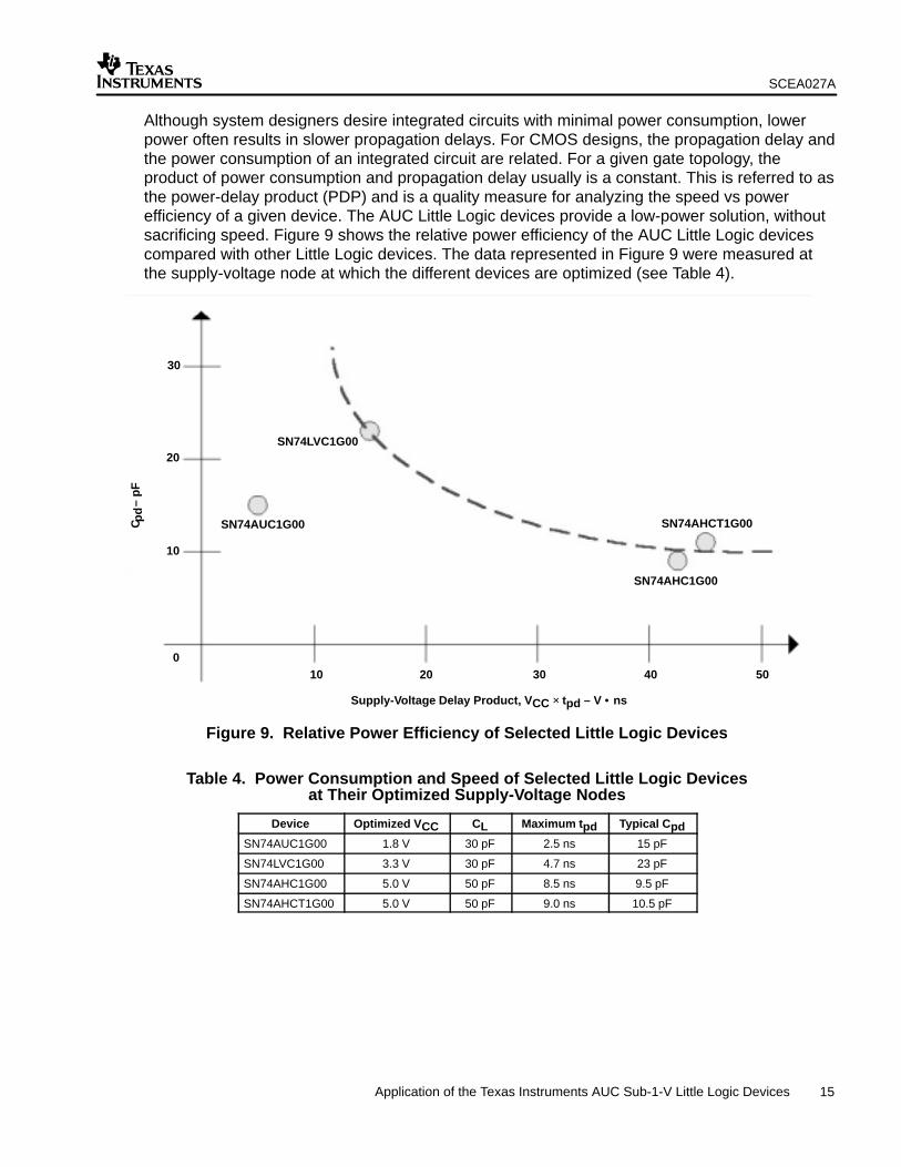
Although system designers desire integrated circuits with minimal power consumption, lowerpower often results in slower propagation delays. For CMOS designs, the propagation delay andthe power consumption of an integrated circuit are related. For a given gate topology, theproduct of power consumption and propagation delay usually is a constant. This is referred to asthe power-delay product (PDP) and is a quality measure for analyzing the speed vs powerefficiency of a given device. The AUC Little Logic devices provide a low-power solution, withoutsacrificing speed. Figure 9 shows the relative power efficiency of the AUC Little Logic devicescompared with other Little Logic devices. The data represented in Figure 9 were measured atthe supply-voltage node at which the different devices are optimized (see Table 4).
Supply-Voltage Delay Product, VCC × tpd – V • ns
100
20 30 40 50
C
– p
Fp
d
10
20
30
SN74AUC1G00
SN74LVC1G00
SN74AHC1G00
SN74AHCT1G00
Figure 9. Relative Power Efficiency of Selected Little Logic Devices
Table 4. Power Consumption and Speed of Selected Little Logic Devicesat Their Optimized Supply-Voltage Nodes
Device Optimized VCC CL Maximum tpd Typical CpdSN74AUC1G00 1.8 V 30 pF 2.5 ns 15 pF
SN74LVC1G00 3.3 V 30 pF 4.7 ns 23 pF
SN74AHC1G00 5.0 V 50 pF 8.5 ns 9.5 pF
SN74AHCT1G00 5.0 V 50 pF 9.0 ns 10.5 pF

SCEA027A
16 Application of the Texas Instruments AUC Sub-1-V Little Logic Devices
4 Design Issues and AUC Little Logic Solutions
4.1 Signal Integrity
As power-supply voltages decrease, signal integrity becomes a major issue. The noise marginrequired for a device to be considered operable reduces proportionately with a reduction inpower-supply voltage. In addition to the requirement for better signal integrity and smaller noisemargins, system designers, especially for portable applications, need a solution that requires noexternal termination (i.e., damping resistors, clamping diodes, etc.). Additional components usevaluable board space, and space also is at a premium in portable applications. The AUC LittleLogic devices provide the best possible solution for systems with these design constraints.
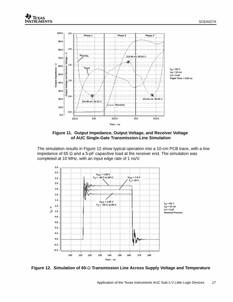
The ULTTL output provides great signal integrity without the need for external termination whendriving traces of moderate length (less than 15 cm). Figure 10 shows a typical applicationenvironment. The driver represents an AUC Little Logic device and the receiver represents aCMOS device whose interface is compatible with the AUC logic levels. The transmission linecorresponds to a PCB trace of 50 Ω to 65 Ω for a portable system application, consisting of shorttrace length (less than 15 cm). During the second phase of the three distinctive transitionalphases of the ULTTL output (see Section 2.1), the AUC output impedance changes to a levelclose to that of the transmission line (see Figure 11), thus minimizing overshoots andundershoots.
Transmission Line
Output Impedance
Output Voltage
Driver Receiver
Receiver Voltage
Ω
Figure 10. Transmission-Line Test Points for Simulations
SCEA027A
17 Application of the Texas Instruments AUC Sub-1-V Little Logic Devices
Time – ns
211.5
2.5
Zo = 65 ΩLg = 10 cmLd = 5 pFFlight Time = 0.64 ns
Ou
tpu
t Im
ped
ance
–
2.0
1.5
1.0
0.5
0.0
212 212.5 213 213.5
211.56 ns; 24.15 Ω
212.84 ns; 65.03 Ω
213.41 ns; 25.04 Ω
100.0
90.0
80.0
70.0
60.0
50.0
40.0
30.0
20.0
10.0
0.0
Ou
tpu
t Vo
ltag
e an
d R
ecei
ver
Volt
age
– V
Ω
Receiver
RTOTAL
YOUT
Phase 1 Phase 2 Phase 3
Figure 11. Output Impedance, Output Voltage, and Receiver Voltage of AUC Single-Gate Transmission-Line Simulation
The simulation results in Figure 12 show typical operation into a 10-cm PCB trace, with a lineimpedance of 65 Ω and a 5-pF capacitive load at the receiver end. The simulation wascompleted at 10 MHz, with an input edge rate of 1 ns/V.
2.0
1.8
1.6
1.4
1.2
1.0
0.8
0.6
0.4
0.2
0.0
100
2.4VCC = 1.95 V
TJ = –40°C to 85°C
V –
VO
–0.2
–0.4
VCC = 1.65 VTJ = –40°C to 85°C
VCC = 1.8 VTJ = 25°C
110 120 130 140 150 160 170 180
Time – ns
Zo = 65 ΩLg = 10 cmLd = 5 pFNominal Process
2.6
2.2
Figure 12. Simulation of 65-Ω Transmission Line Across Supply Voltage and Temperature
SCEA027A
18 Application of the Texas Instruments AUC Sub-1-V Little Logic Devices
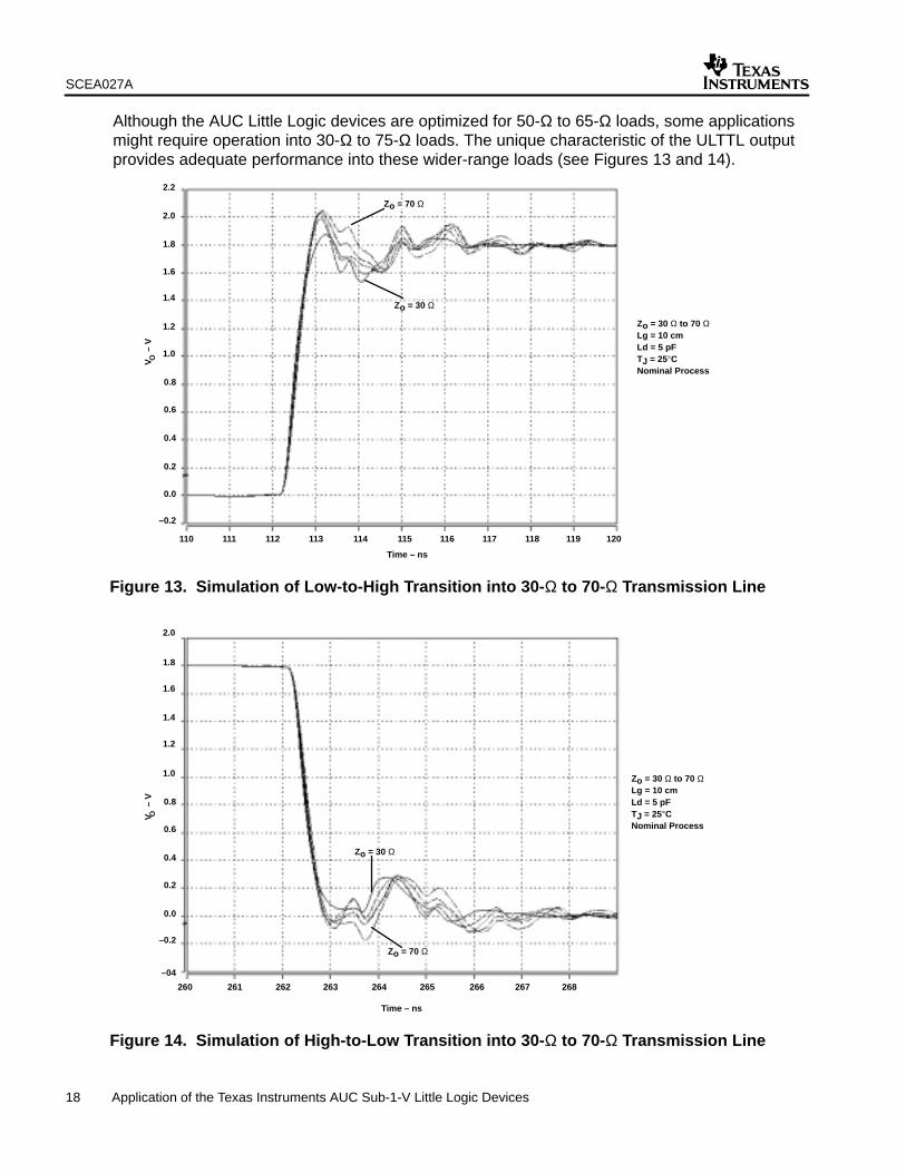
Although the AUC Little Logic devices are optimized for 50-Ω to 65-Ω loads, some applicationsmight require operation into 30-Ω to 75-Ω loads. The unique characteristic of the ULTTL outputprovides adequate performance into these wider-range loads (see Figures 13 and 14).
110
2.0
V
– V
O
111
Zo = 30 Ω to 70 ΩLg = 10 cmLd = 5 pFTJ = 25°CNominal Process
Time – ns
2.2
1.6
1.8
1.4
1.2
1.0
0.8
0.6
0.4
0.2
0.0
–0.2
112 113 114 115 116 117 118 119 120
Zo = 30 Ω
Zo = 70 Ω
Figure 13. Simulation of Low-to-High Transition into 30-Ω to 70-Ω Transmission Line
260
V
– V
O
Zo = 30 Ω to 70 ΩLg = 10 cmLd = 5 pFTJ = 25°CNominal Process
Time – ns
Zo = 30 Ω
Zo = 70 Ω
2.0
1.6
1.8
1.4
1.2
1.0
0.8
0.6
0.4
0.2
0.0
–0.2
–04
261 262 263 264 265 266 267 268
Figure 14. Simulation of High-to-Low Transition into 30-Ω to 70-Ω Transmission Line

SCEA027A
19 Application of the Texas Instruments AUC Sub-1-V Little Logic Devices
4.2 Mixed-Voltage-Mode Data Communication
In designing electronic systems, proper interfaces between buses with incompatible logic levelsmust be provided. Voltage-level translation is necessary to allow the interconnection withflexibility to provide a future migration path to lower-voltage input/output (I/O) levels.
Voltage translation between buses with incompatible logic levels can be accomplished usingAUC Little Logic devices. With a unidirectional AUC driver powered with 1.8-V VCC, datacommunication from 2.5-V or 3.3-V devices can occur (see Figure 15). In this case, the inputs ofthe AUC devices are tolerant of the higher voltages and accept the higher switching levels.Likewise, the outputs of the AUC driver are valid 1.8-V signal levels.
VCC
1.5
0
2.4
0.4
3.3 V
0.8
2.02.3
1.7
1.2
0.7
0.2
0
2.5 V
1.35
1.170.9
0.630.45
0
1.8 V
GND
VOL
VIL
Vt
VIH
VOHVCC
GNDVOL
VIL
Vt
VIH
VOH
VCC
GND
VOL
VIL
Vt
VIH
VOH
VCC = 1.8 V
GND
1.8 V2.5 V or 3.3 V
AUCLittleLogicDevice
Figure 15. Device at 1.8-V VCC, With 2.5-V or 3.3-V Inputs, Showing Switching Levels
Generally, a unidirectional AUC driver powered with 0.8-V, 1.2-V, 1.5-V, or 1.8-V VCC can beused to down-translate from a higher voltage node to the voltage node of the supply voltage.
Similarly, up-translation and down-translation can be achieved by using the SN74AUC1G06 orthe SN74AUC1G07. The SN74AUC1G07 is a noninverting buffer with an open-drain output, andthe SN74AUC1G06 is the inverting buffer (the SN74AUC1G07 plus an extra stage of inversion).These buffers are designed to operate in the 0.8-V to 2.7-V VCC range; however, inputs andoutputs can interface with 3.3-V signals.
This section focuses on the application of the SN74AUC1G07 in voltage-level translation.However, the SN74AUC1G06 can be used in such applications as well, only with an extrainversion.
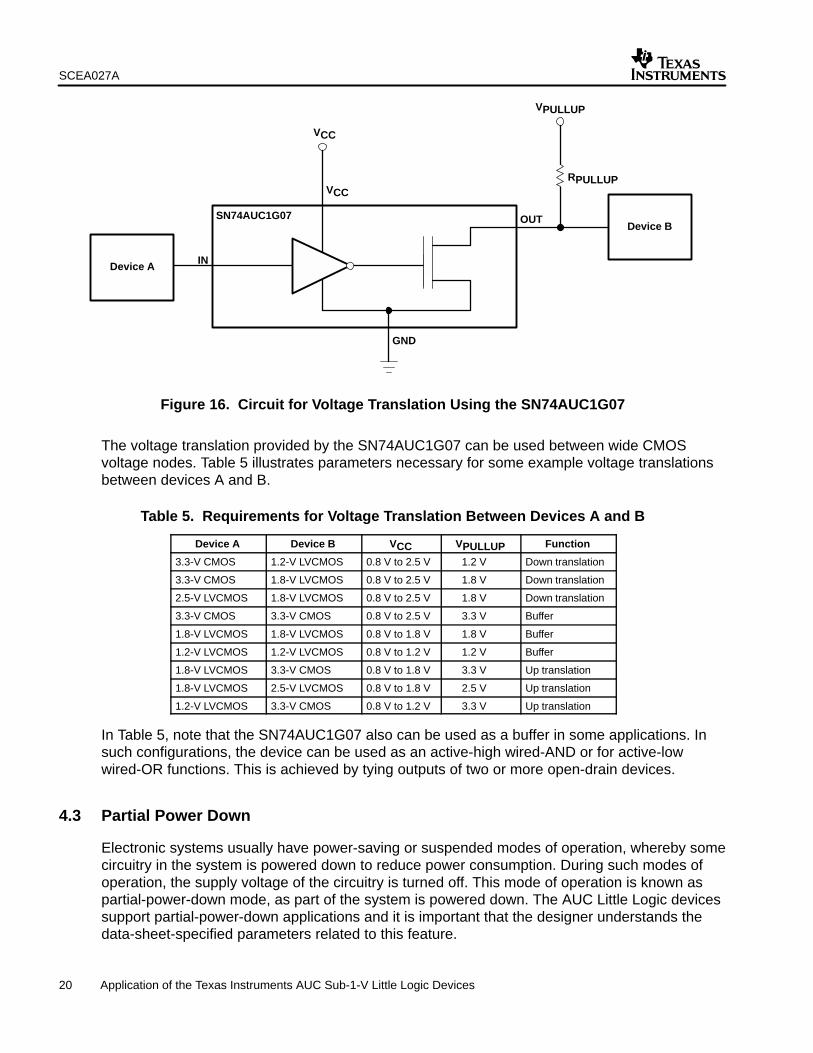
The open-drain feature of the SN74AUC1G07 is useful in voltage translation. The fact that theinput and output structure of this device can accept voltages from 0.8-V to 3.3-V enables thedevice to support voltage translation from a lower voltage to a higher voltage, or vice versa.Without the p-channel pullup on the output structure of the SN74AUC1G07, the entire outputvoltage drops across the n-channel transistor (see Figure 16). With the help of a pullup resistorthat is connected to the designer’s choice of voltage (not exceeding 3.6 V), voltage translation isachieved.
SCEA027A
20 Application of the Texas Instruments AUC Sub-1-V Little Logic Devices
VCC
GND
VPULLUP
RPULLUPVCC
OUT
INDevice A
Device BSN74AUC1G07
Figure 16. Circuit for Voltage Translation Using the SN74AUC1G07
The voltage translation provided by the SN74AUC1G07 can be used between wide CMOSvoltage nodes. Table 5 illustrates parameters necessary for some example voltage translationsbetween devices A and B.
Table 5. Requirements for Voltage Translation Between Devices A and B
Device A Device B VCC VPULLUP Function
3.3-V CMOS 1.2-V LVCMOS 0.8 V to 2.5 V 1.2 V Down translation
3.3-V CMOS 1.8-V LVCMOS 0.8 V to 2.5 V 1.8 V Down translation
2.5-V LVCMOS 1.8-V LVCMOS 0.8 V to 2.5 V 1.8 V Down translation
3.3-V CMOS 3.3-V CMOS 0.8 V to 2.5 V 3.3 V Buffer
1.8-V LVCMOS 1.8-V LVCMOS 0.8 V to 1.8 V 1.8 V Buffer
1.2-V LVCMOS 1.2-V LVCMOS 0.8 V to 1.2 V 1.2 V Buffer
1.8-V LVCMOS 3.3-V CMOS 0.8 V to 1.8 V 3.3 V Up translation
1.8-V LVCMOS 2.5-V LVCMOS 0.8 V to 1.8 V 2.5 V Up translation
1.2-V LVCMOS 3.3-V CMOS 0.8 V to 1.2 V 3.3 V Up translation
In Table 5, note that the SN74AUC1G07 also can be used as a buffer in some applications. Insuch configurations, the device can be used as an active-high wired-AND or for active-lowwired-OR functions. This is achieved by tying outputs of two or more open-drain devices.
4.3 Partial Power Down
Electronic systems usually have power-saving or suspended modes of operation, whereby somecircuitry in the system is powered down to reduce power consumption. During such modes ofoperation, the supply voltage of the circuitry is turned off. This mode of operation is known aspartial-power-down mode, as part of the system is powered down. The AUC Little Logic devicessupport partial-power-down applications and it is important that the designer understands thedata-sheet-specified parameters related to this feature.

SCEA027A
21 Application of the Texas Instruments AUC Sub-1-V Little Logic Devices
To partially power down a device, no direct path from the input to VCC or from the output to VCCcan exist. Consequently, when the device is powered down (VCC = 0 V), independent of the logiclevel at the I/O terminal, no current can flow from the I/O terminal to the power-supply pin, whichis at 0 V. In the partial-powered-down mode, therefore, other devices interfacing with thepowered-down device may be powered up with valid logic levels at the I/O terminals.
With the AUC Little Logic, there is no direct path from the I/O terminal to VCC. Consequently,these devices support partial-power-down modes of operation. This feature is specified on thedata sheet with the Ioff parameter. The Ioff parameter is the maximum leakage current into (or outof) the input (or output) transistors when forcing the input (or output) to 2.7 V and VCC = 0 V.With the AUC Little Logic, Ioff is specified at ±10 µA. This is a very small current and representsleakage current at the I/O terminal.
4.4 Low Power Consumption
The migration to lower voltage nodes is becoming increasingly important in digital electronics,especially with portable and consumer electronics, because of the benefits of reduced powerconsumption. If power consumption is reduced, these electronics can use smaller batteries, thusreducing form factors, while getting the maximum life of the power supply between charges.
The AUC Little Logic devices enable low-power, high-performance designs. The powerconsumption reduction decreases heat dissipation in compact designs. This reduced heatdissipation simplifies heat removal and decreases the amount of package space needed, thussaving valuable board space in compact designs.
Figure 17 shows plots of supply current vs frequency for different AUC Little Logic devices. Foreach of the devices, the test was done with only one input switching from 0 V to 1.8 V at 1 ns/V.Note that the supply current increases with increased input transition. A 1.8-V power supply wasused, and the tests were done at 25°C.
0
1
2
3
4
5
6
7
1 5 10 15 20 30 40 50 60 70 80 90 100 125 150 175
Frequency – MHz
AUC1G14AUC1G00AUC1G04
AUC1G06
I –
mA
CC
Figure 17. ICC vs Frequency for Different AUC Little Logic Devices

SCEA027A
22 Application of the Texas Instruments AUC Sub-1-V Little Logic Devices
Generally, the AUC Little Logic devices consume less power than the corresponding Little Logicdevices of other families. Figure 18 provides a comparison of the supply current vs frequency forthe SN74LVC1G06 and the SN74AUC1G06. Both devices were tested under the sameconditions as those used to obtain the results in Figure 17.
0.00
0.10
0.20
0.30
0.40
0.50
0.60
1 5 10 15 20 30 40 50 60 70 80
LVC1G06
AUC1G06
Frequency – MHz
I –
mA
CC
Figure 18. ICC vs Frequency for SN74AUC1G06 and SN74LVC1G06 Devices
5 Package Information
The devices discussed in this application report are available in a variety of packages, includingSOT-23 (DBV), SC-70 (DCK), tin-lead (SnPb) NanoStar (YEA), and lead-free NanoFree(YZA). TI’s Little Logic Data Book, literature number SCED010, lists devices and packages inwhich they are available. The mechanical data information for these packages is provided inAppendix B of this application report.
The mechanical data for the YEA and YZA packages are the same. The only difference betweenthe two packages is that the YEA package is leaded, while the YZA package is lead-free. TheNanoStar and NanoFree packages comply with JEDEC MO-211.
SCEA027A
23 Application of the Texas Instruments AUC Sub-1-V Little Logic Devices
6 Features and Benefits
Table 6 summarizes the features and benefits of AUC Little Logic devices.
Table 6. Features and Benefits of AUC Little Logic Devices
FEATURES BENEFITS
Low power consumption Use in portable electronics and battery-operated systems
Supports Ioff at inputs Use in applications that require partial power-down modes
3.6-V I/O tolerant Use in level-translation applications. Eases migration to lower-voltage nodes. Enhances systemsafety.
Sub-1-V operable Flexibility for future migration. Operable at lower-voltage nodes means less power consumption.
Small low-profile packages Saves board space. Simplify large PCB routing. Use as quick fix for design errors.
Cost effective Inexpensive compared to redesign. Used as quick fix for design errors. Reduces time-to-marketand maximized design investment in all types of electronic systems.
7 Conclusion
The AUC Little Logic devices provide simple cost-effective solutions for portable electronics andbattery-operated systems and facilitates quick fixes in system design errors. The devices areoptimized at 1.8 V and are compatible with 2.5-V, 1.5-V, 1.2-V, and 0.8-V systems. The AUCfamily features TI’s ULTTL output circuitry, 3.6-V I/O tolerance, low power consumptioncapability, and partial power-down support. Features, electrical characteristics, and applicationsof the AUC Little Logic devices are presented in this application report.
8 Frequently Asked Questions (FAQs)
Question 1: What is AUC?
Answer: The advanced ultra-low-voltage CMOS (AUC) is the new logic family that is optimized at 1.8 V, has an operating voltage range from 0.8 V to 2.5 V, and is tolerant of 3.3-V input and output voltages.
Question 2: What is ULTTL?
Answer: The ultra-low-voltage transistor-transistor logic (ULTTL) is a new interface driver designed for high-speed with low EMI noise, low power consumption, and optimalsignal integrity.
Question 3: How do I get copies of the AUC family data sheets and samples?
Answer: The AUC family data sheets can be obtained by accessing http://www.ti.com. Samples of the AUC devices can be obtained by contacting your local TI sales representative.
Question 4: How do I get copies of AUC family SPICE and IBIS models?
Answer: The SPICE models for AUC devices can be obtained by contacting your local TI sales representative. The IBIS model can be obtained by accessing http://www.ti.com.
SCEA027A
24 Application of the Texas Instruments AUC Sub-1-V Little Logic Devices
Question 5: What are the advantages of migrating to the AUC family?
Answer: The advantages of migrating to the AUC family include:
• Lowered power consumption enables use in portable electronics andbattery-operated systems.
• Partial-power-down mode is supported.
• Level-translation is feasible and migration to lower-voltage nodes is easy.
• Future migration to sub-1-V applications is possible.
• Board space is saved and large-PCB routing is simplified.
• Capability for fixing design errors is flexible and redesign cost is lower.
Question 6: What should I do if it appears that the device is producing a noisy signal?
Answer: The most common reason an AUC device may appear to be producing a noisy signal is that the outputs have not been terminated properly. To reduce or eliminate reflections that are inherent with long trace lengths and transmission lines, one of five techniques must be used to match the impedance of the transmission line and thereby properly terminate the output. These five techniques are: single-resistor termination, parallel split-resistor termination, series-resistor termination, resistor-and-capacitor termination, and diode termination. For a detailed explanation of the techniques and the advantages anddisadvantages of each method, refer to the Advanced Schottky Load Management Application Report.[3]
Question 7: What is the maximum voltage the input pin of an AUC Little Logic can sustain when the device is powered down or when the device is powered up?
Answer: The AUC Little Logic devices are 3.6-V tolerant at the inputs. Therefore, within the supply-voltage operational range (0.8 V = VCC = 2.7 V), the input voltage canbe as high as 3.6 V. Further, the AUC Little Logic devices have the Ioff feature. Therefore, if VCC = 0 V, the inputs can tolerate a 3.6-V signal.
Question 8: What is the maximum voltage the output pin of an AUC Little Logic device can sustain when the device is powered down, and how can this information be inferred from the data sheet?
Answer: With older family devices, there is a parasitic diode connected from the output to VCC. With those devices, if VCC = 0 V and the output is driven about 1 V above VCC, the diode is forward biased and conducts current from the output pin to the VCC pin. Under this condition, the device can be damaged. Therefore, the data sheet of a device with a power-clamp diode has a positive limit on the output clamp current (IOK).
The AUC Little Logic, however, have no parasitic diode from the output to VCC. The data sheets specify an absolute maximum rating IOK of –50 mA, with no positive limit for this specification. Therefore, the output can be driven above VCC, but caution should be taken to ensure that the IOK limit is not exceeded when the output is driven below GND.

SCEA027A
25 Application of the Texas Instruments AUC Sub-1-V Little Logic Devices
The above explanation applies only for the absolute maximum rating of the device. Under the recommended operating conditions, the AUC Little Logic devices with outputs incapable of being placed in the high-impedance state are recommended to be between 0 V and VCC.
Question 9: What is the maximum operating frequency of the AUC Little Logic devices?
Answer: The maximum operating frequency of a device depends upon the load that the AUC device is driving. Using the specified data sheet load, the AUC Little Logic devices have been tested in the laboratory to operate at frequencies greater than 175 MHz.
9 References1. The Bergeron Method: A Graphical Method for Determining Line Reflections in Transient
Phenomena, application report, literature number SDYA014.
2. Little Logic Data Book (SCED010), November 2001.
3. Advanced Schottky Load Management, application report, literature number SDYA016.
10 Glossary
ac Alternating current
ACB ac branch
AUC Advanced ultra-low-voltage CMOS
CMOS Complementary metal-oxide silicon; a device technology that has balanced drive outputs and low power consumption
dc Direct current
DCB dc branch
EMI Electromagnetic interference
IBIS I/O buffer information specification
Ioff The maximum leakage current into/out of the input/output transistors when forcing the input/output to 2.7 V and VCC = 0 V
IOH High-level output current. The current out of an output with input conditions applied that, according to the product specification, establishes a high level at the output.
IOK Output clamp current. The absolute maximum current that can be sourced from an output pin when the voltage is taken below 0 V
IOL Low-level output current. The current into an output with input conditions applied that,according to the product specification, establishes a low level at the output.

SCEA027A
26 Application of the Texas Instruments AUC Sub-1-V Little Logic Devices
JEDEC Joint Electron Device Engineering Council
LOP Lower-output transistor
LVCMOS Low-voltage complementary metal-oxide silicon
PCB Printed circuit board
PDP Power-delay product
ron On-channel resistance
SPICE Simulation program with integrated circuit emphasis
TI Texas Instruments
TLB Transmission-line branch
tpd Propagation delay time. The time between the specified reference points on the inputand output voltage waveforms with the output changing from one defined level (high or low) to the other defined level (tpd = tPHL or tPLH).
tPHL Propagation delay time, high-to-low level output. The time between the specified reference points on the input and output voltage waveforms, with the output changingfrom the defined high level to the defined low level.
tPLH Propagation delay time, low-to-high level output. The time between the specified reference points on the input and output voltage waveforms, with the output changingfrom the defined low level to the defined high level
TTL Transistor-transistor logic
ULTTL Ultra-low-voltage transistor-transistor logic
UOP Upper-output transistor
VOH High-level output voltage. The voltage at an output terminal with input conditions applied such that, according to product specification, it establishes a high level at the output.
VOL Low-level output voltage. The voltage at an output terminal with input conditions applied such that, according to product specification, it establishes a low level at the output.
SCEA027A
27 Application of the Texas Instruments AUC Sub-1-V Little Logic Devices
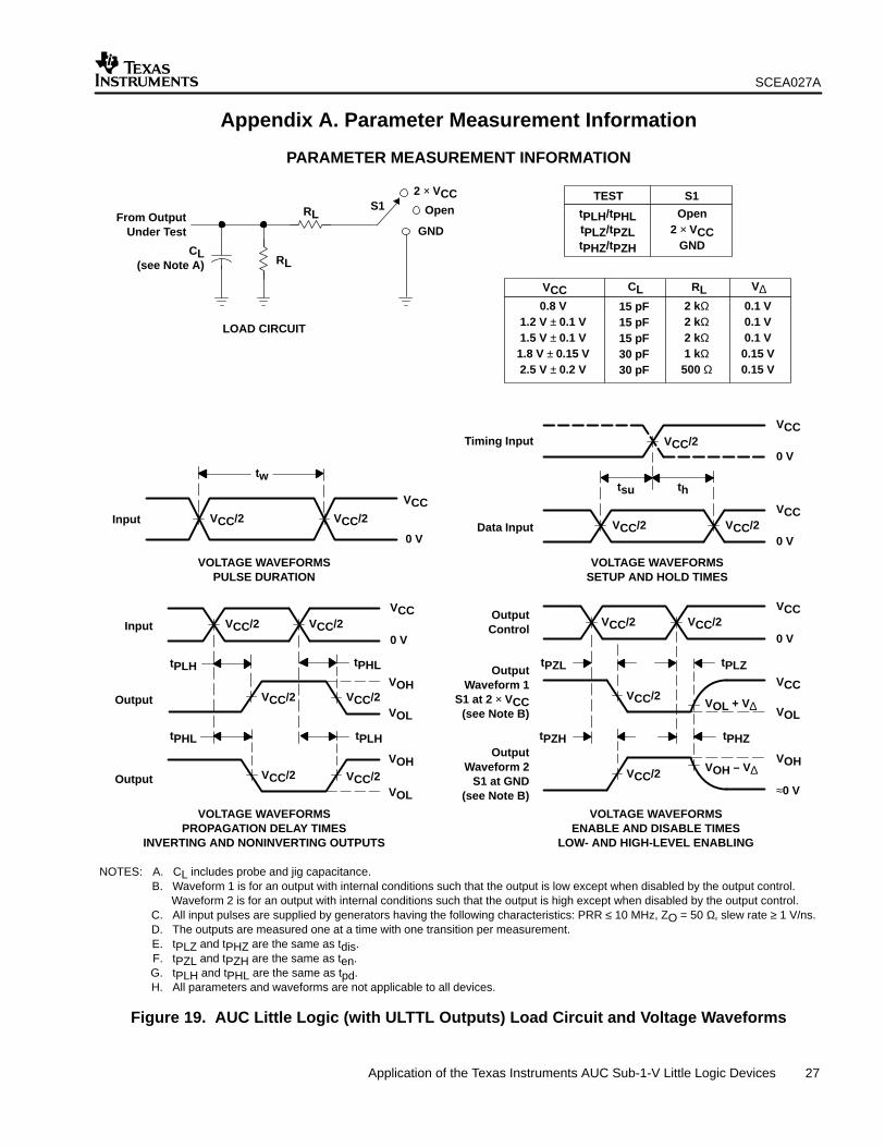
Appendix A. Parameter Measurement Information
PARAMETER MEASUREMENT INFORMATION
VCC/2
thtsu
From OutputUnder Test
CL(see Note A)
LOAD CIRCUIT
S12 × VCC
Open
GND
RL
RL
Data Input
Timing InputVCC
0 V
VCC
0 V0 V
tw
Input
VOLTAGE WAVEFORMSSETUP AND HOLD TIMES
VOLTAGE WAVEFORMSPROPAGATION DELAY TIMES
INVERTING AND NONINVERTING OUTPUTS
VOLTAGE WAVEFORMSPULSE DURATION
tPLH
tPHL
tPHL
tPLH
VOH
VOH
VOL
VOL
VCC
0 VInput
OutputWaveform 1
S1 at 2 × VCC(see Note B)
OutputWaveform 2
S1 at GND(see Note B)
VOL
VOH
tPZL
tPZH
tPLZ
tPHZ
VCC
0 V
VOL + V∆
VOH – V∆
≈0 V
VCC
VOLTAGE WAVEFORMSENABLE AND DISABLE TIMES
LOW- AND HIGH-LEVEL ENABLING
Output
Output
tPLH/tPHLtPLZ/tPZLtPHZ/tPZH
Open2 × VCC
GND
TEST S1
NOTES: A. CL includes probe and jig capacitance.B. Waveform 1 is for an output with internal conditions such that the output is low except when disabled by the output control.
Waveform 2 is for an output with internal conditions such that the output is high except when disabled by the output control.C. All input pulses are supplied by generators having the following characteristics: PRR ≤ 10 MHz, ZO = 50 Ω, slew rate ≥ 1 V/ns.D. The outputs are measured one at a time with one transition per measurement.E. tPLZ and tPHZ are the same as tdis.F. tPZL and tPZH are the same as ten.G. tPLH and tPHL are the same as tpd.H. All parameters and waveforms are not applicable to all devices.
OutputControl
VCC/2 VCC/2
VCC/2 VCC/2
VCC/2 VCC/2
VCC/2
VCC/2 VCC/2
VCC/2
VCC/2
VCC/2
VCC
VCC/2
VCC/2
0.8 V1.2 V ± 0.1 V1.5 V ± 0.1 V1.8 V ± 0.15 V2.5 V ± 0.2 V
2 kΩ2 kΩ2 kΩ1 kΩ500 Ω
VCC RL0.1 V0.1 V0.1 V0.15 V0.15 V
V∆CL15 pF15 pF15 pF30 pF30 pF
Figure 19. AUC Little Logic (with ULTTL Outputs) Load Circuit and Voltage Waveforms

SCEA027A
28 Application of the Texas Instruments AUC Sub-1-V Little Logic Devices
PARAMETER MEASUREMENT INFORMATION(OPEN DRAIN)
VCC/2
thtsu
From OutputUnder Test
CL(see Note A)
LOAD CIRCUIT
S12 × VCC
Open
GND
RL
RL
Data Input
Timing InputVCC
0 V
VCC
0 V0 V
tw
Input
VOLTAGE WAVEFORMSSETUP AND HOLD TIMES
VOLTAGE WAVEFORMSPROPAGATION DELAY TIMES
INVERTING AND NONINVERTING OUTPUTS
VOLTAGE WAVEFORMSPULSE DURATION
tPLH
tPHL
tPHL
tPLH
VOH
VOH
VOL
VOL
VCC
0 VInput
OutputWaveform 1
S1 at 2 × VCC(see Note B)
OutputWaveform 2
S1 at 2 × VCC(see Note B)
VOL
VOH
tPZL
tPZH
tPLZ
tPHZ
VCC
0 V
VOL + V∆
VOH – V∆
≈0 V
VCC
VOLTAGE WAVEFORMSENABLE AND DISABLE TIMES
LOW- AND HIGH-LEVEL ENABLING
Output
Output
tPZL(see Note F)
tPLZ(see Note G)tPHZ/tPZH
2 × VCC
2 × VCC
2 × VCC
TEST S1
NOTES: I. CL includes probe and jig capacitance.J. Waveform 1 is for an output with internal conditions such that the output is low except when disabled by the output control.
Waveform 2 is for an output with internal conditions such that the output is high except when disabled by the output control.K. All input pulses are supplied by generators having the following characteristics: PRR ≤ 10 MHz, ZO = 50 Ω, slew rate ≥ 1 V/ns.L. The outputs are measured one at a time with one transition per measurement.M. For open-drain outputs, tPLZ and tPZL are the same as tpd.N. tPZL is measured at VCC/2.O. tPLZ is measured at VOL + V∆.P. All parameters and waveforms are not applicable to all devices.
OutputControl
VCC/2 VCC/2
VCC/2 VCC/2
VCC/2 VCC/2
VCC/2
VCC/2 VCC/2
VCC/2
VCC/2
VCC/2
VCC
VCC/2
VCC/2
0.8 V1.2 V ± 0.1 V1.5 V ± 0.1 V1.8 V ± 0.15 V2.5 V ± 0.2 V
2 kΩ2 kΩ2 kΩ1 kΩ500 Ω
VCC RL0.1 V0.1 V0.1 V0.15 V0.15 V
V∆CL15 pF15 pF15 pF30 pF30 pF
Figure 20. AUC Little Logic (with Open-Drain Outputs) Load Circuit and Voltage Waveforms

SCEA027A
29 Application of the Texas Instruments AUC Sub-1-V Little Logic Devices
Appendix B. Mechanical Data
DBV (R-PDSO-G5)PLASTIC SMALL-OUTLINE
0,10
M0,200,95
0°–8°
0,25
0,350,55
Gage Plane
0,15 NOM
4073253-4/G 01/02
2,603,00
0,500,30
1,501,70
45
31
2,803,00
0,951,45
0,05 MIN
Seating Plane
NOTES: A. All linear dimensions are in millimeters.B. This drawing is subject to change without notice.C. Body dimensions do not include mold flash or protrusion.D. Falls within JEDEC MO-178
Figure 21. Plastic Small Outline (DBV)

SCEA027A
30 Application of the Texas Instruments AUC Sub-1-V Little Logic Devices
DCK (R-PDSO-G5)PLASTIC SMALL-OUTLINE PACKAGE
0,10
M0,100,65
0°–8° 0,460,26
0,13 NOM
4093553-2/D 01/02
0,150,30
1,401,10
2,401,80
45
2,151,85
1 3
1,100,80
0,100,00
Seating Plane
0,15
Gage Plane
NOTES: A. All linear dimensions are in millimeters.B. This drawing is subject to change without notice.C. Body dimensions do not include mold flash or protrusion.D. Falls within JEDEC MO-203
Figure 22. Plastic Small Outline (DCK)

SCEA027A
31 Application of the Texas Instruments AUC Sub-1-V Little Logic Devices
YEA (R-XBGA-N5)DIE-SIZE BALL GRID ARRAY
C
Seating Plane
0,50 MAX
4203167-2/B 11/2001
1,351,45
0,850,95
1 2
A
B
C
0,50
0.25
1.00
0.50
0.190.15
5X
0.050.05
AM CM C
B
B
Pin A1 Index Area
A
C0.150.10
0.05
0.35 MAX
NOTES: A. All linear dimensions are in millimeters.B. This drawing is subject to change without notice.C. NanoStar package configuration.D. Package complies to JEDEC MO-211.
Figure 23. Die-Size Ball Grid Array (YEA or YZA)
NanoStar is a trademark of Texas Instruments.
IMPORTANT NOTICE
Texas Instruments Incorporated and its subsidiaries (TI) reserve the right to make corrections, modifications,enhancements, improvements, and other changes to its products and services at any time and to discontinueany product or service without notice. Customers should obtain the latest relevant information before placingorders and should verify that such information is current and complete. All products are sold subject to TI’s termsand conditions of sale supplied at the time of order acknowledgment.
TI warrants performance of its hardware products to the specifications applicable at the time of sale inaccordance with TI’s standard warranty. Testing and other quality control techniques are used to the extent TIdeems necessary to support this warranty. Except where mandated by government requirements, testing of allparameters of each product is not necessarily performed.
TI assumes no liability for applications assistance or customer product design. Customers are responsible fortheir products and applications using TI components. To minimize the risks associated with customer productsand applications, customers should provide adequate design and operating safeguards.
TI does not warrant or represent that any license, either express or implied, is granted under any TI patent right,copyright, mask work right, or other TI intellectual property right relating to any combination, machine, or processin which TI products or services are used. Information published by TI regarding third–party products or servicesdoes not constitute a license from TI to use such products or services or a warranty or endorsement thereof.Use of such information may require a license from a third party under the patents or other intellectual propertyof the third party, or a license from TI under the patents or other intellectual property of TI.
Reproduction of information in TI data books or data sheets is permissible only if reproduction is withoutalteration and is accompanied by all associated warranties, conditions, limitations, and notices. Reproductionof this information with alteration is an unfair and deceptive business practice. TI is not responsible or liable forsuch altered documentation.
Resale of TI products or services with statements different from or beyond the parameters stated by TI for thatproduct or service voids all express and any implied warranties for the associated TI product or service andis an unfair and deceptive business practice. TI is not responsible or liable for any such statements.
Mailing Address:
Texas InstrumentsPost Office Box 655303Dallas, Texas 75265
Copyright 2002, Texas Instruments Incorporated