
Application of Line Scan Technology for Defect Inspection ...
17
1 Sensors and Materials, Vol. 33, No. # (2021) 1–## MYU Tokyo S & M #### * Corresponding author: e-mail: [email protected] https://doi.org/10.18494/SAM.2021.3251 ISSN 0914-4935 © MYU K.K. https://myukk.org/ Application of Line Scan Technology for Defect Inspection in Plain Dyed Fabric Yu-Liang Chen, Chia-Wei Tsai, Fan-Siou Ding, and Quang-Cherng Hsu* Department of Mechanical Engineering, National Kaohsiung University of Science and Technology, No. 415, Jiangong Rd., Sanmin Dist., Kaohsiung City 80778, Taiwan (Received January 1, 2021; accepted March 3, 2021; online published April 22, 2021) Keywords: automatic optical inspection, defect inspection, fabric dyeing and finishing, line scan Fabrics are susceptible to defects caused by various factors during the dyeing and finishing processes. Fabric defects are mostly detected through manual visual inspection. Under the influence of fatigue from long working hours and human error in general, this method results in misjudgment and missed defects. Certain difficulties are encountered in the development of automated optical inspection (AOI) machines because large pieces of fabric must be inspected at high speed. In this study, an AOI system was developed. The image acquisition system consisted of an IDS industrial camera equipped with a sensor for fabric defect inspection and a line scan function, as well as a white light-emitting diode (LED) light bar. The parameters were configured and calibrated using uEye Cockpit software. The inspection mechanism of the proposed machine was a roller device that simulated fabric production. Under continuous rotation of the roller, images were captured using the camera and then were combined to form a two-dimensional plane image. Long-term inspection was performed simultaneously. The line scan settings were a pixel clock (PCLK)S rate of 474 MHz and 10 scan lines per single scan when the tangential rotation velocity of the roller simulation was 0.9 m/s. The minimum vertical distortion of the acquired image was 1.658 mm when the total image length was 210 mm. Uneven illumination from the nonlinear light source resulted in the generation of noise in the captured images, which was eliminated through the combination of posterization and closing, with only a slight loss of defect features. Overall, the proposed AOI system effectively detected the defects. The minimum width of black defects that could be detected in the dyed and finished dark fabrics was 0.24 mm. 1. Introduction Fabrics, including clothing, are an essential part of life. Before white fabrics become colorful textile materials, they must first undergo dyeing and finishing processes. Inspection, mainly visual, must then be performed to ensure that the fabrics meet certain requirements and contain no defects. The fatigue caused by long working hours can result in human errors, such as misjudged or missed defects. This system necessitates a substantial amount of labor and the production efficiency is low. This version has been created for advance publication by formatting the accepted manuscript. Some editorial changes may be made to this version.
Transcript of Application of Line Scan Technology for Defect Inspection ...
1Sensors and Materials, Vol. 33, No. # (2021) 1–##MYU Tokyo
S & M ####
*Corresponding author: e-mail: [email protected]://doi.org/10.18494/SAM.2021.3251
ISSN 0914-4935 © MYU K.K.https://myukk.org/
Application of Line Scan Technology for Defect Inspection in Plain Dyed Fabric
Yu-Liang Chen, Chia-Wei Tsai, Fan-Siou Ding, and Quang-Cherng Hsu*
Department of Mechanical Engineering, National Kaohsiung University of Science and Technology,No. 415, Jiangong Rd., Sanmin Dist., Kaohsiung City 80778, Taiwan
(Received January 1, 2021; accepted March 3, 2021; online published April 22, 2021)
Keywords: automaticopticalinspection,defectinspection,fabricdyeingandfinishing,linescan
Fabrics are susceptible to defects caused by various factors during the dyeing and finishing processes. Fabric defects are mostly detected through manual visual inspection. Under the influence of fatigue from long working hours and human error in general, this method results in misjudgment and missed defects. Certain difficulties are encountered in the development of automated optical inspection (AOI) machines because large pieces of fabric must be inspected at high speed. In this study, an AOI system was developed. The image acquisition system consisted of an IDS industrial camera equipped with a sensor for fabric defect inspection and a line scan function, as well as a white light-emitting diode (LED) light bar. The parameters were configured and calibrated using uEye Cockpit software. The inspection mechanism of the proposed machine was a roller device that simulated fabric production. Under continuous rotation of the roller, images were captured using the camera and then were combined to form a two-dimensional plane image. Long-term inspection was performed simultaneously. The line scan settings were a pixel clock (PCLK)S rate of 474 MHz and 10 scan lines per single scan when the tangential rotation velocity of the roller simulation was 0.9 m/s. The minimum vertical distortion of the acquired image was 1.658 mm when the total image length was 210 mm. Uneven illumination from the nonlinear light source resulted in the generation of noise in the captured images, which was eliminated through the combination of posterization and closing, with only a slight loss of defect features. Overall, the proposed AOI system effectively detected the defects. The minimum width of black defects that could be detected in the dyed and finished dark fabrics was 0.24 mm.
1. Introduction
Fabrics, including clothing, are an essential part of life. Before white fabrics become colorful textile materials, they must first undergo dyeing and finishing processes. Inspection, mainly visual, must then be performed to ensure that the fabrics meet certain requirements and contain no defects. The fatigue caused by long working hours can result in human errors, such as misjudged or missed defects. This system necessitates a substantial amount of labor and the production efficiency is low.
This version has been created for advance publication by formatting the accepted manuscript.Some editorial changes may be made to this version.
2 Sensors and Materials, Vol. 33, No. # (2021)
Regarding detection systems, the use of line scan cameras to capture high-speed images and to detect various objects has been described frequently in the literature. To improve the accuracy and speed of conventional video-based traffic cameras, Xu et al.(1) developed a vehicle inspection system that used line scan cameras. Specifically, two line scan cameras were used for image capture. The contour area of the vehicle in an image was extracted through a wavelet transform, and vehicle speed was estimated by examining curve relationships. In general, compared with conventional video-based traffic cameras, which require a longer detection time, line scan cameras can more accurately detect objects moving at high speed. Deutschl et al.(2) used an automatic system for the detection of railway surface defects. The system included a color line scan camera and involved the use of a spectral imaging program, which can detect defects such as peeling, cracks, grooves, or fractures through image processing (with an image resolution of 0.3 × 0.5 mm2 at 60 km/h). Suppitaksakul and Rattakorn(3) proposed a method for counting the number of corrugated cardboard sheets by using a line scan camera and image processing techniques. The gray scale values of edge images obtained from a line scanner were converted into binary images. The strip line features of the surface were extracted by a morphological examination. The fluted areas of the cardboard were subjected to blob analysis. Next, the center of the detected area was identified and the number of corrugated cardboard sheets was calculated. The counting was accurate, and the errors on the slitter and cutoff sides were 2 and 3 cm, respectively. Wang et al.(4) established an image capture system by mounting a columnar asphalt mixture on a rotating stage with a line scan camera. The built-in setup of the camera and Camera Configuration Tool Plus software were used to adjust the capture cycle parameters. The images captured under various light settings were compared to ensure that the optimal settings were used. Deng et al.(5) established a plane detection system in which two-line scanning charge-coupled device cameras were used to detect various defects (e.g., holes, dust, and scratches) on tinplate surfaces under wide-field illumination. Two illumination modules were used for detection. The dark field was suitable for detecting scattered defects, whereas the bright field was mainly suitable for detecting defects involving reflected or absorbed light, such as pits and pinholes. Through the training and application of a self-organizing map and a neural network, the defects were inspected at a speed of 1.4 m/s and the probability of correct classification was 95.45%. Kwon et al.(6) used a line scanner to inspect black resin-coated steel. The image acquisition procedure included pretreatment, threshold selection, binarization, and postprocessing. Specifically, the pretreatment involved average filtering, image segmentation, and the consideration of the weighting gain concerning black defects. After binarization, the small amount of noise was eliminated through switching operations. The results indicated that the algorithm enabled highly accurate inspection. Bandara et al.(7) developed a system for detecting fabric defects through image processing techniques by a neural network. The lighting system consisted of illuminated panels of different colors, including ultraviolet lamps with red, green, and blue light. The lighting elements used depended on the kind of defects. For example, fabrics with oil stain defects must be detected and classified using ultraviolet lamps.
Sensors and Materials, Vol. 33, No. # (2021) 3
Ren et al.(8) applied a method involving the use of the edge of an image to quickly detect and locate defects on circuit boards and increase the detection speed on printed circuit boards (PCBs). The algorithm accounted for the gray scale characteristics of the edge images. Specifically, differences in the characteristics of standard images and images with defects were used to identify and classify the defects. Defects such as short circuits, open circuits, burrs, and holes were rapidly detected. Iyshwerya et al.(9) used machine vision for the real-time detection of surface defects in mild steel welding chips. They developed methods that effectively reduced noise and involved prefiltering and postfiltering to detect surface defects such as dents and rust. Line scanners were used in the hardware, and quartz tungsten lamps were the light source. The detection accuracy was 96.31%. Zheng and Wang(10) used an image subtraction algorithm and machine vision and image processing techniques to detect fabric defects. Their system removed the original image to identify the defects in the image of the piece to be inspected. Inverse binarization was performed to determine the defect characteristics. The peak recognition accuracy was 92% and the error rate was less than 5%. Chen et al.(11) proposed a machine-vision-based approach for the study of surface defects in steel plates and planning the grinding path of a robot. The gray scale values of the background and steel plate images were compared, and the steel plate was separated through mean filtering, binarization, and edge detection, thereby yielding the positions of flaws in the steel plate. Baygin et al.(12) proposed a contactless defect detection method for PCBs. A camera was used to capture images of the PCBs. Various image processing methods, such as color conversion (RGB to YUV), Gaussian filtering, Otsu thresholding, edge detection, the circle Hough transform, and the black-hat transform, were used to compare the images of the standard components with those of the components to be measured. Wang et al.(13) used an automated optical inspection (AOI) system to detect defects (e.g., blind holes and defects plated through holes) in PCBs. Several procedures were conducted, including image correction, image segmentation, and comparison of the drilling specifications for the holes. The defects (e.g., missing holes, offsets, and excessive holes) were detected within 10 s with a tolerance of approximately 5 µm. DaSilva et al.(14) applied an automatic optical system to detect defective solder joints on PCBs. The images were transilluminated into binary images by reducing the saturation and enhancing the contrast and brightness. Inverse binarization was also performed. Next, the solder feature frame was selected. Set as the region of interest (ROI), it was trimmed and analyzed to obtain the solder yield rate. Lin et al.(15) proposed an automated optical method for inspecting integrated circuit chips in a tray. A line scan camera with a linear motor was used. The locations of all the defects were obtained on the basis of the positioning of the chips. They were then marked using a laser. In the present study, we developed an automatic optical system involving computer vision methods and high-speed industrial cameras to inspect dyed and finished fabrics. Data analysis was also performed. The present findings serve as a reference for future developments in smart manufacturing.
4 Sensors and Materials, Vol. 33, No. # (2021)
2. Materials and Methods
The image acquisition system used for fabric inspection in this study comprised an IDS industrial camera with a line scan function and a white light-emitting diode (LED) light bar. Parameter setting and calibration were conducted using uEye Cockpit software. The captured images were processed using ROI selection, posterization, thresholding, and closing. Finally, contour detection was performed, and the contour area was used to calculate the defect size.
2.1 Image acquisition system
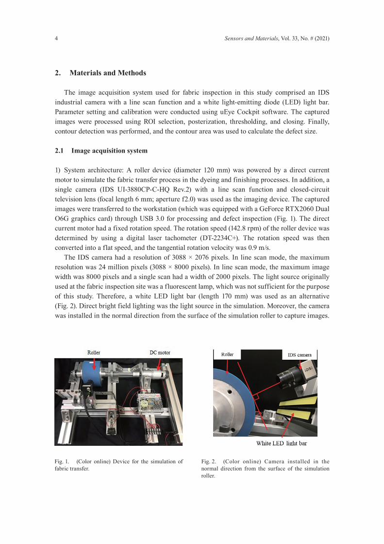
1) System architecture: A roller device (diameter 120 mm) was powered by a direct current motor to simulate the fabric transfer process in the dyeing and finishing processes. In addition, a single camera (IDS UI-3880CP-C-HQ Rev.2) with a line scan function and closed-circuit television lens (focal length 6 mm; aperture f2.0) was used as the imaging device. The captured images were transferred to the workstation (which was equipped with a GeForce RTX2060 Dual O6G graphics card) through USB 3.0 for processing and defect inspection (Fig. 1). The direct current motor had a fixed rotation speed. The rotation speed (142.8 rpm) of the roller device was determined by using a digital laser tachometer (DT-2234C+). The rotation speed was then converted into a flat speed, and the tangential rotation velocity was 0.9 m/s. The IDS camera had a resolution of 3088 × 2076 pixels. In line scan mode, the maximum resolution was 24 million pixels (3088 × 8000 pixels). In line scan mode, the maximum image width was 8000 pixels and a single scan had a width of 2000 pixels. The light source originally used at the fabric inspection site was a fluorescent lamp, which was not sufficient for the purpose of this study. Therefore, a white LED light bar (length 170 mm) was used as an alternative (Fig. 2). Direct bright field lighting was the light source in the simulation. Moreover, the camera was installed in the normal direction from the surface of the simulation roller to capture images.
Fig. 1. (Color online) Device for the simulation of fabric transfer.
Fig. 2. (Color online) Camera installed in the normal direction from the surface of the simulation roller.
Sensors and Materials, Vol. 33, No. # (2021) 5
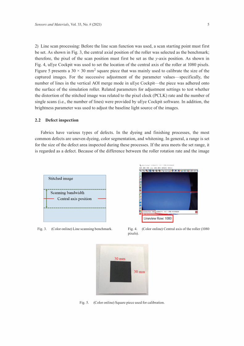
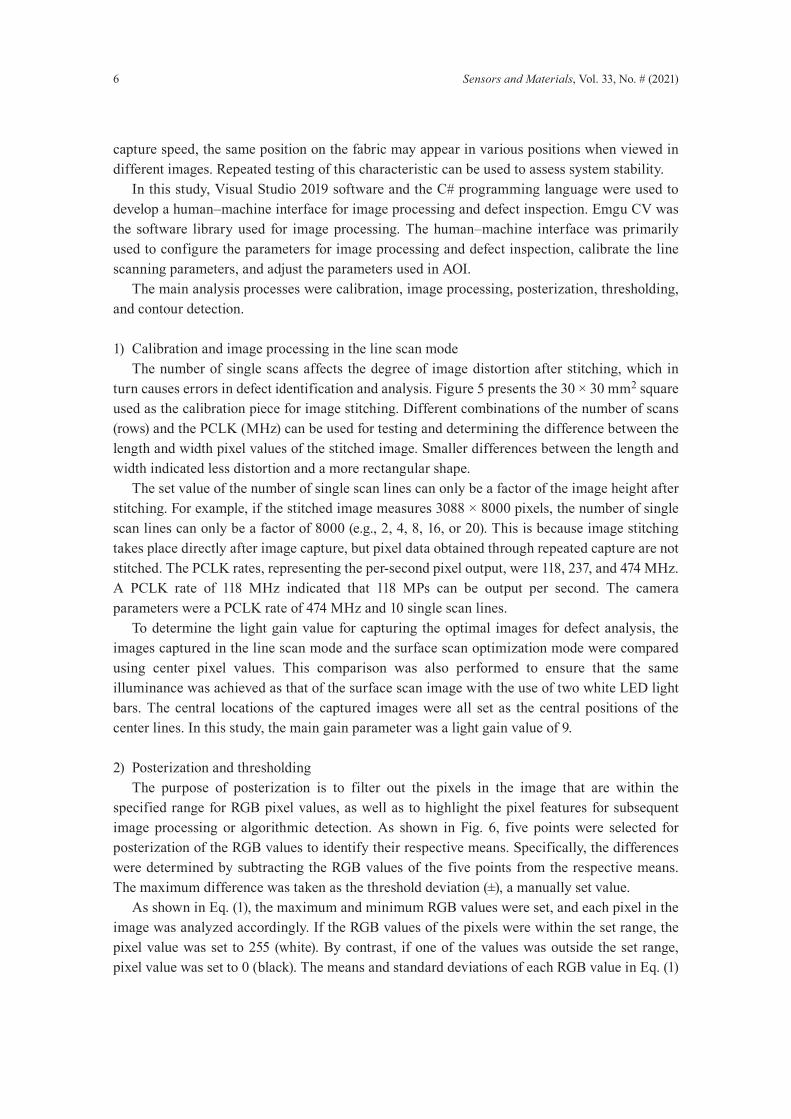
2) Line scan processing: Before the line scan function was used, a scan starting point must first be set. As shown in Fig. 3, the central axial position of the roller was selected as the benchmark; therefore, the pixel of the scan position must first be set as the y-axis position. As shown in Fig. 4, uEye Cockpit was used to set the location of the central axis of the roller at 1080 pixels. Figure 5 presents a 30 × 30 mm2 square piece that was mainly used to calibrate the size of the captured images. For the successive adjustment of the parameter values—specifically, the number of lines in the vertical AOI merge mode in uEye Cockpit—the piece was adhered onto the surface of the simulation roller. Related parameters for adjustment settings to test whether the distortion of the stitched image was related to the pixel clock (PCLK) rate and the number of single scans (i.e., the number of lines) were provided by uEye Cockpit software. In addition, the brightness parameter was used to adjust the baseline light source of the images.
2.2 Defect inspection
Fabrics have various types of defects. In the dyeing and finishing processes, the most common defects are uneven dyeing, color segmentation, and whitening. In general, a range is set for the size of the defect area inspected during these processes. If the area meets the set range, it is regarded as a defect. Because of the difference between the roller rotation rate and the image
Fig. 3. (Color online) Line scanning benchmark. Fig. 4. (Color online) Central axis of the roller (1080 pixels).
Fig. 5. (Color online) Square piece used for calibration.
6 Sensors and Materials, Vol. 33, No. # (2021)
capture speed, the same position on the fabric may appear in various positions when viewed in different images. Repeated testing of this characteristic can be used to assess system stability. In this study, Visual Studio 2019 software and the C# programming language were used to develop a human–machine interface for image processing and defect inspection. Emgu CV was the software library used for image processing. The human–machine interface was primarily used to configure the parameters for image processing and defect inspection, calibrate the line scanning parameters, and adjust the parameters used in AOI. The main analysis processes were calibration, image processing, posterization, thresholding, and contour detection.
1) Calibration and image processing in the line scan mode The number of single scans affects the degree of image distortion after stitching, which in turn causes errors in defect identification and analysis. Figure 5 presents the 30 × 30 mm2 square used as the calibration piece for image stitching. Different combinations of the number of scans (rows) and the PCLK (MHz) can be used for testing and determining the difference between the length and width pixel values of the stitched image. Smaller differences between the length and width indicated less distortion and a more rectangular shape. The set value of the number of single scan lines can only be a factor of the image height after stitching. For example, if the stitched image measures 3088 × 8000 pixels, the number of single scan lines can only be a factor of 8000 (e.g., 2, 4, 8, 16, or 20). This is because image stitching takes place directly after image capture, but pixel data obtained through repeated capture are not stitched. The PCLK rates, representing the per-second pixel output, were 118, 237, and 474 MHz. A PCLK rate of 118 MHz indicated that 118 MPs can be output per second. The camera parameters were a PCLK rate of 474 MHz and 10 single scan lines. To determine the light gain value for capturing the optimal images for defect analysis, the images captured in the line scan mode and the surface scan optimization mode were compared using center pixel values. This comparison was also performed to ensure that the same illuminance was achieved as that of the surface scan image with the use of two white LED light bars. The central locations of the captured images were all set as the central positions of the center lines. In this study, the main gain parameter was a light gain value of 9.
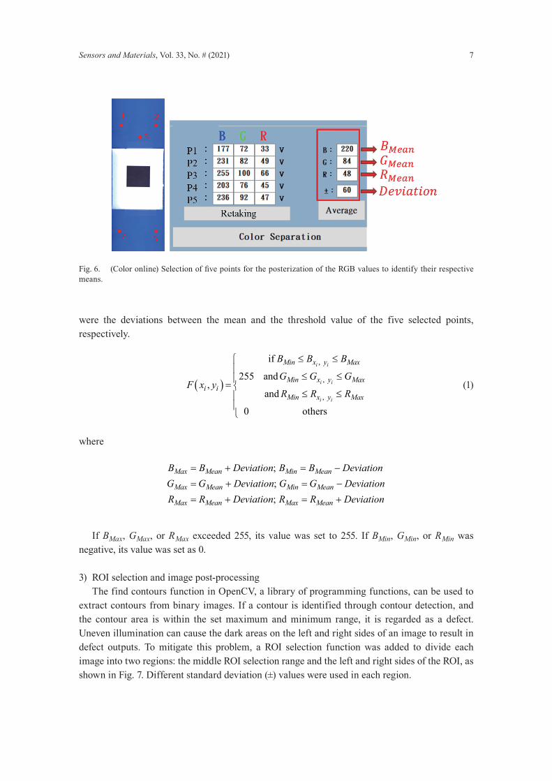
2) Posterization and thresholding The purpose of posterization is to filter out the pixels in the image that are within the specified range for RGB pixel values, as well as to highlight the pixel features for subsequent image processing or algorithmic detection. As shown in Fig. 6, five points were selected for posterization of the RGB values to identify their respective means. Specifically, the differences were determined by subtracting the RGB values of the five points from the respective means. The maximum difference was taken as the threshold deviation (±), a manually set value. As shown in Eq. (1), the maximum and minimum RGB values were set, and each pixel in the image was analyzed accordingly. If the RGB values of the pixels were within the set range, the pixel value was set to 255 (white). By contrast, if one of the values was outside the set range, pixel value was set to 0 (black). The means and standard deviations of each RGB value in Eq. (1)
Sensors and Materials, Vol. 33, No. # (2021) 7
were the deviations between the mean and the threshold value of the five selected points, respectively.
( )
,
,
,
if
255 and ,
and
0 others
i i
i i
i i
Min x y Max
Min x y Maxi i
Min x y Max
B B B
G G GF x y
R R R
≤ ≤
≤ ≤= ≤ ≤
(1)
where
;;;
Max Mean Min Mean
Max Mean Min Mean
Max Mean Max Mean
B B Deviation B B DeviationG G Deviation G G DeviationR R Deviation R R Deviation
= + = −
= + = −
= + = +
If BMax, GMax, or RMax exceeded 255, its value was set to 255. If BMin, GMin, or RMin was negative, its value was set as 0.
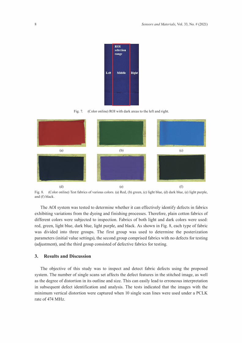
3) ROI selection and image post-processing The find contours function in OpenCV, a library of programming functions, can be used to extract contours from binary images. If a contour is identified through contour detection, and the contour area is within the set maximum and minimum range, it is regarded as a defect. Uneven illumination can cause the dark areas on the left and right sides of an image to result in defect outputs. To mitigate this problem, a ROI selection function was added to divide each image into two regions: the middle ROI selection range and the left and right sides of the ROI, as shown in Fig. 7. Different standard deviation (±) values were used in each region.
Fig.6. (Coloronline)SelectionoffivepointsfortheposterizationoftheRGBvaluestoidentifytheirrespectivemeans.
8 Sensors and Materials, Vol. 33, No. # (2021)
The AOI system was tested to determine whether it can effectively identify defects in fabrics exhibiting variations from the dyeing and finishing processes. Therefore, plain cotton fabrics of different colors were subjected to inspection. Fabrics of both light and dark colors were used: red, green, light blue, dark blue, light purple, and black. As shown in Fig. 8, each type of fabric was divided into three groups. The first group was used to determine the posterization parameters (initial value settings), the second group comprised fabrics with no defects for testing (adjustment), and the third group consisted of defective fabrics for testing.
3. Results and Discussion
The objective of this study was to inspect and detect fabric defects using the proposed system. The number of single scans set affects the defect features in the stitched image, as well as the degree of distortion in its outline and size. This can easily lead to erroneous interpretation in subsequent defect identification and analysis. The tests indicated that the images with the minimum vertical distortion were captured when 10 single scan lines were used under a PCLK rate of 474 MHz.
Fig. 7. (Color online) ROI with dark areas to the left and right.
Fig. 8. (Color online) Test fabrics of various colors. (a) Red, (b) green, (c) light blue, (d) dark blue, (e) light purple, and (f) black.
(a) (b) (c)
(d) (e) (f)
Sensors and Materials, Vol. 33, No. # (2021) 9
3.1 PCLK rates and number of single scans
The number of single scans used affects the amount of distortion in images captured in line scanning mode. Therefore, a square calibration piece measuring 30 mm × 30 mm and the PCLK rate were set to determine the size difference of the calibration piece in the image. A higher number of single scans (rows) indicated a greater pixel length obtained in a single scan. As shown in Eq, (2), the camera frame rate was 58 Hz. Under a sample setting of 3088 × 2000 pixels, a PCLK rate of 358 MHz was established to be sufficient for the output.
PCLK = H total × V total × Frame Rate (2)
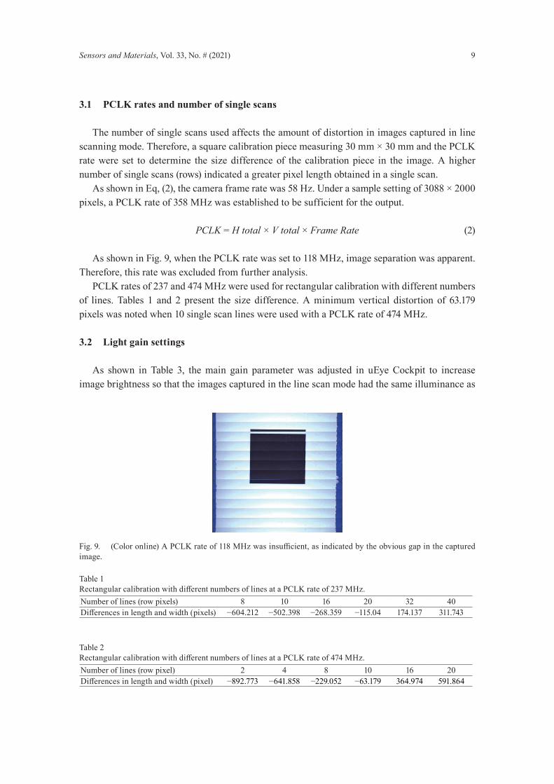
As shown in Fig. 9, when the PCLK rate was set to 118 MHz, image separation was apparent. Therefore, this rate was excluded from further analysis. PCLK rates of 237 and 474 MHz were used for rectangular calibration with different numbers of lines. Tables 1 and 2 present the size difference. A minimum vertical distortion of 63.179 pixels was noted when 10 single scan lines were used with a PCLK rate of 474 MHz.
3.2 Light gain settings
As shown in Table 3, the main gain parameter was adjusted in uEye Cockpit to increase image brightness so that the images captured in the line scan mode had the same illuminance as
Fig.9. (Coloronline)APCLKrateof118MHzwasinsufficient,asindicatedbytheobviousgapinthecapturedimage.
Table 1RectangularcalibrationwithdifferentnumbersoflinesataPCLKrateof237MHz.Number of lines (row pixels) 8 10 16 20 32 40Differencesinlengthandwidth(pixels) −604.212 −502.398 −268.359 −115.04 174.137 311.743
Table 2RectangularcalibrationwithdifferentnumbersoflinesataPCLKrateof474MHz.Number of lines (row pixel) 2 4 8 10 16 20Differencesinlengthandwidth(pixel) −892.773 −641.858 −229.052 −63.179 364.974 591.864
10 Sensors and Materials, Vol. 33, No. # (2021)
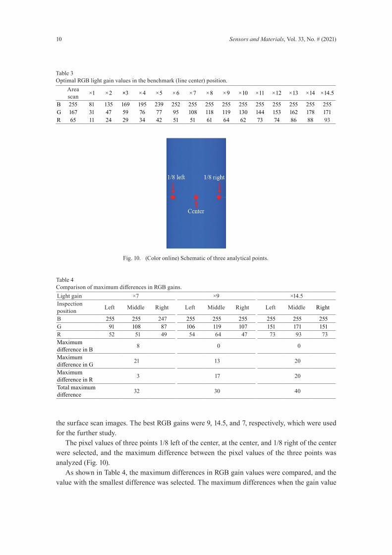
the surface scan images. The best RGB gains were 9, 14.5, and 7, respectively, which were used for the further study. The pixel values of three points 1/8 left of the center, at the center, and 1/8 right of the center were selected, and the maximum difference between the pixel values of the three points was analyzed (Fig. 10). As shown in Table 4, the maximum differences in RGB gain values were compared, and the value with the smallest difference was selected. The maximum differences when the gain value
Table 4ComparisonofmaximumdifferencesinRGBgains.Light gain ×7 ×9 ×14.5Inspection position Left Middle Right Left Middle Right Left Middle Right
B 255 255 247 255 255 255 255 255 255G 91 108 87 106 119 107 151 171 151R 52 51 49 54 64 47 73 93 73Maximum differenceinB 8 0 0
Maximum differenceinG 21 13 20
Maximum differenceinR 3 17 20
Total maximum difference 32 30 40
Fig. 10. (Color online) Schematic of three analytical points.
Table 3Optimal RGB light gain values in the benchmark (line center) position.
Area scan ×1 ×2 ×3 ×4 ×5 ×6 ×7 ×8 ×9 ×10 ×11 ×12 ×13 ×14 ×14.5
B 255 81 135 169 195 239 252 255 255 255 255 255 255 255 255 255G 167 31 47 59 76 77 95 108 118 119 130 144 153 162 178 171R 65 11 24 29 34 42 51 51 61 64 62 73 74 86 88 93
Sensors and Materials, Vol. 33, No. # (2021) 11
was 9 for R, G, and B were 17, 13, and 0 (medium, minimum, and minimum), respectively. The sum of the maximum differences (30) was also the smallest of the three gain values. Therefore, a light gain value of 9 was used as the main gain parameter.
3.3 Uneven illumination and image post-processing
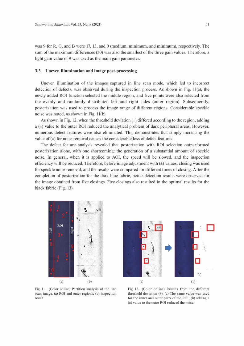
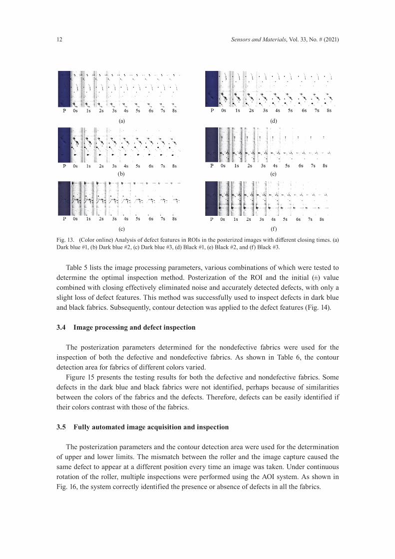
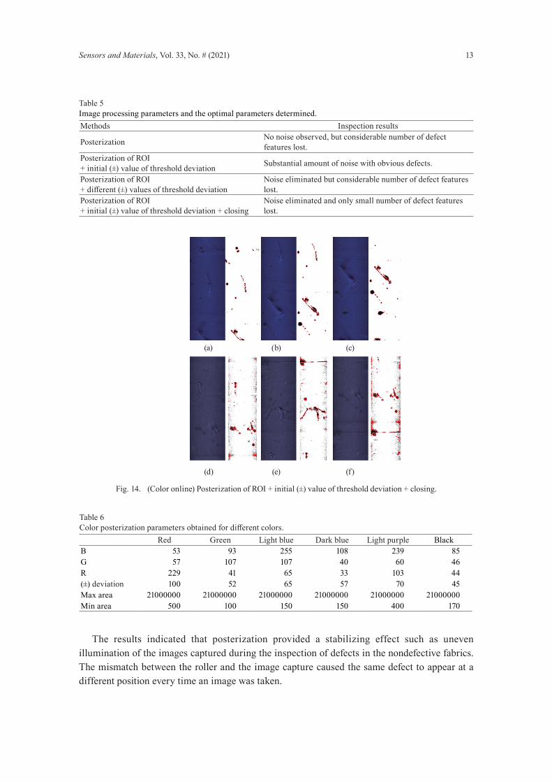
Uneven illumination of the images captured in line scan mode, which led to incorrect detection of defects, was observed during the inspection process. As shown in Fig. 11(a), the newly added ROI function selected the middle region, and five points were also selected from the evenly and randomly distributed left and right sides (outer region). Subsequently, posterization was used to process the image range of different regions. Considerable speckle noise was noted, as shown in Fig. 11(b). As shown in Fig. 12, when the threshold deviation (±) differed according to the region, adding a (±) value to the outer ROI reduced the analytical problem of dark peripheral areas. However, numerous defect features were also eliminated. This demonstrates that simply increasing the value of (±) for noise removal causes the considerable loss of defect features. The defect feature analysis revealed that posterization with ROI selection outperformed posterization alone, with one shortcoming: the generation of a substantial amount of speckle noise. In general, when it is applied to AOI, the speed will be slowed, and the inspection efficiency will be reduced. Therefore, before image adjustment with (±) values, closing was used for speckle noise removal, and the results were compared for different times of closing. After the completion of posterization for the dark blue fabric, better detection results were observed for the image obtained from five closings. Five closings also resulted in the optimal results for the black fabric (Fig. 13).
Fig. 11. (Color online) Partition analysis of the line scan image. (a) ROI and outer regions; (b) inspection result.
(a) (b)
Fig.12. (Color online) Results from the differentthreshold deviation (±). (a) The same value was used for the inner and outer parts of the ROI; (b) adding a (±) value to the outer ROI reduced the noise.
(a) (b)
12 Sensors and Materials, Vol. 33, No. # (2021)
Fig.13. (Coloronline)AnalysisofdefectfeaturesinROIsintheposterizedimageswithdifferentclosingtimes.(a)Dark blue #1, (b) Dark blue #2, (c) Dark blue #3, (d) Black #1, (e) Black #2, and (f) Black #3.
(a) (d)
(b) (e)
(c) (f)
Table 5 lists the image processing parameters, various combinations of which were tested to determine the optimal inspection method. Posterization of the ROI and the initial (±) value combined with closing effectively eliminated noise and accurately detected defects, with only a slight loss of defect features. This method was successfully used to inspect defects in dark blue and black fabrics. Subsequently, contour detection was applied to the defect features (Fig. 14).
3.4 Image processing and defect inspection
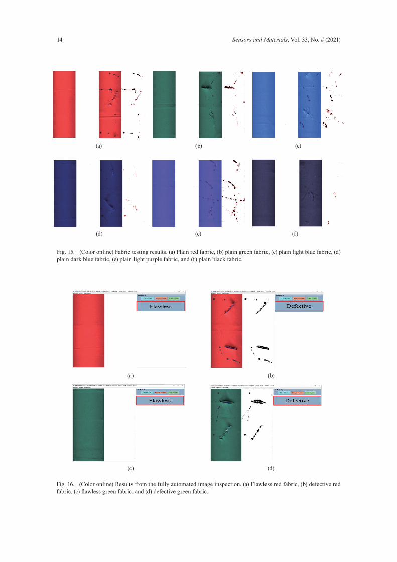
The posterization parameters determined for the nondefective fabrics were used for the inspection of both the defective and nondefective fabrics. As shown in Table 6, the contour detection area for fabrics of different colors varied. Figure 15 presents the testing results for both the defective and nondefective fabrics. Some defects in the dark blue and black fabrics were not identified, perhaps because of similarities between the colors of the fabrics and the defects. Therefore, defects can be easily identified if their colors contrast with those of the fabrics.
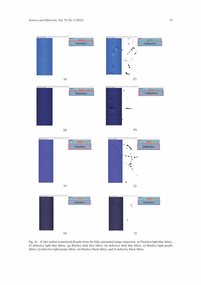
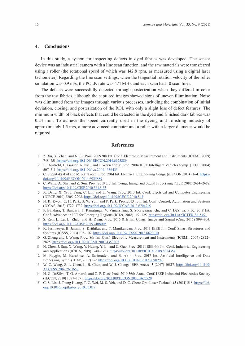
3.5 Fully automated image acquisition and inspection
The posterization parameters and the contour detection area were used for the determination of upper and lower limits. The mismatch between the roller and the image capture caused the same defect to appear at a different position every time an image was taken. Under continuous rotation of the roller, multiple inspections were performed using the AOI system. As shown in Fig. 16, the system correctly identified the presence or absence of defects in all the fabrics.
Sensors and Materials, Vol. 33, No. # (2021) 13
Table 5Image processing parameters and the optimal parameters determined.Methods Inspection results
Posterization No noise observed, but considerable number of defect features lost.
Posterization of ROI + initial (±) value of threshold deviation Substantial amount of noise with obvious defects.
Posterization of ROI +different(±)valuesofthresholddeviation
Noise eliminated but considerable number of defect features lost.
Posterization of ROI + initial (±) value of threshold deviation + closing
Noise eliminated and only small number of defect features lost.
Fig. 14. (Color online) Posterization of ROI + initial (±) value of threshold deviation + closing.
(d) (e) (f)
(a) (b) (c)
Table 6Colorposterizationparametersobtainedfordifferentcolors.
Red Green Light blue Dark blue Light purple BlackB 53 93 255 108 239 85G 57 107 107 40 60 46R 229 41 65 33 103 44(±) deviation 100 52 65 57 70 45Max area 21000000 21000000 21000000 21000000 21000000 21000000Min area 500 100 150 150 400 170
The results indicated that posterization provided a stabilizing effect such as uneven illumination of the images captured during the inspection of defects in the nondefective fabrics. The mismatch between the roller and the image capture caused the same defect to appear at a different position every time an image was taken.
14 Sensors and Materials, Vol. 33, No. # (2021)
Fig. 15. (Color online) Fabric testing results. (a) Plain red fabric, (b) plain green fabric, (c) plain light blue fabric, (d) plain dark blue fabric, (e) plain light purple fabric, and (f) plain black fabric.
(a) (b) (c)
(d) (e) (f)
(a) (b)
(c) (d)
Fig. 16. (Color online) Results from the fully automated image inspection. (a) Flawless red fabric, (b) defective red fabric,(c)flawlessgreenfabric,and(d)defectivegreenfabric.
Sensors and Materials, Vol. 33, No. # (2021) 15
(e) (f)
(g) (h)
(l)
(i) (j)
(k)
Fig. 16. (Color online) (continued) Results from the fully automated image inspection. (e) Flawless light blue fabric, (f)defectivelightbluefabric,(g)flawlessdarkbluefabric,(h)defectivedarkbluefabric,(i)flawlesslightpurplefabric,(j)defectivelightpurplefabric,(k)flawlessblackfabric,and(l)defectiveblackfabric.
16 Sensors and Materials, Vol. 33, No. # (2021)
4. Conclusions
In this study, a system for inspecting defects in dyed fabrics was developed. The sensor device was an industrial camera with a line scan function, and the raw materials were transferred using a roller (the rotational speed of which was 142.8 rpm, as measured using a digital laser tachometer). Regarding the line scan settings, when the tangential rotation velocity of the roller simulation was 0.9 m/s, the PCLK rate was 474 MHz and each scan had 10 scan lines. The defects were successfully detected through posterization when they differed in color from the test fabrics, although the captured images showed signs of uneven illumination. Noise was eliminated from the images through various processes, including the combination of initial deviation, closing, and posterization of the ROI, with only a slight loss of defect features. The minimum width of black defects that could be detected in the dyed and finished dark fabrics was 0.24 mm. To achieve the speed currently used in the dyeing and finishing industry of approximately 1.5 m/s, a more advanced computer and a roller with a larger diameter would be required.
References
1 Z. Xu, X. Zhao, and N. Li: Proc. 2009 9th Int. Conf. Electronic Measurement and Instruments (ICEMI, 2009) 748–751. https://doi.org/10.1109/iEECON.2014.6925889
2 E. Deutschl, C. Gasser, A. Niel, and J. Werschonig: Proc. 2004 IEEE Intelligent Vehicles Symp. (IEEE, 2004) 507–511. https://doi.org/10.1109/ivs.2004.1336435
3 C. Suppitaksakul and M. Rattakorn: Proc. 2014 Int. Electrical Engineering Congr. (iEECON, 2014) 1–4. https://doi.org/10.1109/iEECON.2014.6925889
4 C. Wang, A. Sha, and Z. Sun: Proc. 2010 3rd Int. Congr. Image and Signal Processing (CISP, 2010) 2614–2618. https://doi.org/10.1109/CISP.2010.5648155
5 X. Deng, X. Ye, J. Fang, C. Lin, and L. Wang: Proc. 2010 Int. Conf. Electrical and Computer Engineering (ICECE 2010) 2205–2208. https://doi.org/10.1109/iCECE.2010.543
6 N. K. Kwon, C. H. Park, S. W. Yun, and P. Park: Proc.2013 13th Int. Conf. Control, Automation and Systems (ICCAS, 2013) 1729–1732. https://doi.org/10.1109/ICCAS.2013.6704215
7 P. Bandara, T. Bandara, T. Ranatunga, V. Vimarshana, S. Sooriyaarachchi, and C. DeSilva: Proc. 2018 Int. Conf. Advances in ICT for Emerging Regions (ICTer, 2018) 119–125. https://doi.org/10.1109/ICTER.8615491
8 S. Ren, L. Lu, L. Zhao, and H. Duan: Proc. 2015 8Th Int. Congr. Image and Signal (Cisp, 2015) 899–903. https://doi.org/10.1109/CISP.2015.7408005
9 K. Iyshwerya, B. Janani, S. Krithika, and T. Manikandan: Proc. 2013 IEEE Int. Conf. Smart Structures and Systems (ICSSS, 2013) 103–107. https://doi.org/10.1109/ICSSS.2013.6623010
10 G. Zheng and J. Wang: Proc. 8th Int. Conf. Electronic Measurement and Instruments (ICEMI, 2007) 2822–2825. https://doi.org/10.1109/ICEMI.2007.4350807
11 N. Chen, J. Sun, X. Wang, Y. Huang, Y. Li, and C. Guo: Proc. 2019 IEEE 6th Int. Conf. Industrial Engineering and Applications (ICIEA, 2019) 1748–1753. https://doi.org/10.1109/ICIEA.2019.8834354
12 M. Baygin, M. Karakose, A. Sarimaden, and E. Akin: Proc. 2017 Int. Artificial Intelligence and DataProcessing Symp. (IDAP, 2017) 1–5 https://doi.org/10.1109/IDAP.2017.8090292
13 W. C. Wang, S. L. Chen, L. B. Chen, and W. J. Chang: IEEE Access 5 (2017) 10817. https://doi.org/10.1109/ACCESS.2016.2631658
14 H. G. DaSilva, T. G. Amaral, and O. P. Dias: Proc. 2010 36th Annu. Conf. IEEE Industrial Electronics Society (IECON, 2010) 1087–1091. https://doi.org/10.1109/IECON.2010.5675520
15 C. S. Lin, J. Tsung Huang, T. C. Wei, M. S. Yeh, and D. C. Chen: Opt. Laser Technol. 43 (2011) 218. https://doi.org/10.1016/j.optlastec.2010.06.017
Sensors and Materials, Vol. 33, No. # (2021) 17
About the Authors
Yu-Liang Chen received his B.S. degree from Ta Hwa University of Science and Technology, Taiwan, in 2000 and his M.S. degree from Southern Taiwan University of Science and Technology, Taiwan, in 2006. Since 2012, he has been a Ph.D. student at National Kaohsiung University of Science and Technology, From 2014 to 2019, he was a senior design engineer at Enplas, mainly responsible for IC reliability testing sockets, Taiwan. Since 2020, he has been a section manager in Chipbond Technology Corporation, mainly responsible for COF design and departmental management.
Chia-Wei Tsai received his B.S. degree from Chung Yuan Christian University, Taiwan, in 2018 and his M.S. degree from National Kaohsiung University of Sciences and Technology, Taiwan, in 2020. He is currently working as an engineer in Chipbond Technology Corporation, mainly responsible for image recognition and artificial-intelligence-related fields. ([email protected])
Fan-Siou Ding received her B.S. degree from National Pingtung University of Science and Technology, Taiwan, in 2019. She is studying for her M.S. degree at National Kaohsiung University of Science and Technology. Her research interest is machine vision. ([email protected])
Quang-Cherng Hsu received his B.S., M.S., and Ph.D. degrees from National Cheng Kung University, Taiwan, in 1985, 1987, and 1991, respectively. From 1993 to 1995, he was an engineer at Metal Industries Research & Development Centre, Taiwan. From 1995 to 2005, he was an associate professor at National Kaohsiung University of Applied Sciences, Taiwan. Since 2005, he has been a professor at National Kaohsiung University of Science and Technology, Taiwan. His research interests are in metal forming, machine vision, and nano-engineering. ([email protected])