
Application Note: Virtex-5 FPGAs 16-Channel, DDR … Transmitter XAPP855 (v1.0) October 13, 2006 4 R...
43
XAPP855 (v1.0) October 13, 2006 www.xilinx.com 1 © 2006 Xilinx, Inc. All rights reserved. All Xilinx trademarks, registered trademarks, patents, and further disclaimers are as listed at http://www.xilinx.com/legal.htm . PowerPC is a trademark of IBM Inc. All other trademarks and registered trademarks are the property of their respective owners. All specifications are subject to change without notice. NOTICE OF DISCLAIMER: Xilinx is providing this design, code, or information "as is." By providing the design, code, or information as one possible implementation of this feature, application, or standard, Xilinx makes no representation that this implementation is free from any claims of infringement. You are responsible for obtaining any rights you may require for your implementation. Xilinx expressly disclaims any warranty whatsoever with respect to the adequacy of the implementation, including but not limited to any warranties or representations that this implementation is free from claims of infringement and any implied warranties of merchantability or fitness for a particular purpose. Summary This application note describes a 16-channel, source-synchronous LVDS interface operating at double data rate (DDR). The transmitter (TX) requires 16 LVDS pairs for data and one LVDS pair for the forwarded clock. The transmitter operates at 8:1 serialization on each of the 16 data channels. The receiver (RX) also requires 16 LVDS pairs for data and one LVDS pair for the source-synchronous clock input. The receiver operates at 1:8 deserialization on each of the 16 data channels. The timing of the receiver is described in depth and characterized in hardware. Introduction The design described in the application note targets a Virtex™-5 FPGA, taking advantage of the ChipSync™ features available in every I/O of all Virtex-5 devices. These features include the ability to dynamically adjust the delay of the datapaths in the receiver with 75 ps resolution. Using this dynamic delay feature, the receiver in this application note escapes the limitations of static setup/hold timing by creating its own dynamic setup/hold timing. The interface calibrates out process variations by finding the optimal setup/hold timing for each individual device. Figure 1 shows a Virtex-5 DDR interface talking to a DDR interface in another device that can be either an ASIC or an FPGA with support for a 16-channel DDR interface. Since this is a source-synchronous link, the receivers of both devices receive their clock from the TX side of the other device. The clock sources for the transmitters could come from a number of places in the backend systems, such as an oscillator on the PCB. Since each of the 16 data channels on the serial side of the interface runs at 8:1 serialization, the data on the parallel side of the DDR interface is 128 bits. The stand-alone DDR interface described in this application note does not include user constraints (includes no UCF file). To evaluate the performance of this DDR interface in hardware, a separate bit error rate tester (BERT) is also available for download (Figure 2, page 2). Application Note: Virtex-5 FPGAs XAPP855 (v1.0) October 13, 2006 16-Channel, DDR LVDS Interface with Per-Channel Alignment Author: Greg Burton R Figure 1: Full-Duplex, 16-Channel DDR Link between a Virtex-5 Device and Another Device with a 16-Channel DDR Interface Backend System Device With DDR Interface Backend System TXDATA TX Clock Source TX Parallel Data RX Parallel Data TX Clock Source TX Parallel Data 128 RX Parallel Data RXDATA TXCLK RXCLK 16 16 128 128 128 X855_01_072406 XAPP855 DDR Interface in Virtex-5 FPGA
Transcript of Application Note: Virtex-5 FPGAs 16-Channel, DDR … Transmitter XAPP855 (v1.0) October 13, 2006 4 R...

XAPP855 (v10) October 13 2006 wwwxilinxcom 1
copy 2006 Xilinx Inc All rights reserved All Xilinx trademarks registered trademarks patents and further disclaimers are as listed at httpwwwxilinxcomlegalhtm PowerPC is atrademark of IBM Inc All other trademarks and registered trademarks are the property of their respective owners All specifications are subject to change without notice
NOTICE OF DISCLAIMER Xilinx is providing this design code or information as is By providing the design code or information as one possible implementation of this featureapplication or standard Xilinx makes no representation that this implementation is free from any claims of infringement You are responsible for obtaining any rights you may requirefor your implementation Xilinx expressly disclaims any warranty whatsoever with respect to the adequacy of the implementation including but not limited to any warranties orrepresentations that this implementation is free from claims of infringement and any implied warranties of merchantability or fitness for a particular purpose
Summary This application note describes a 16-channel source-synchronous LVDS interface operating at double data rate (DDR) The transmitter (TX) requires 16 LVDS pairs for data and one LVDS pair for the forwarded clock The transmitter operates at 81 serialization on each of the 16 data channels The receiver (RX) also requires 16 LVDS pairs for data and one LVDS pair for the source-synchronous clock input The receiver operates at 18 deserialization on each of the 16 data channels The timing of the receiver is described in depth and characterized in hardware
Introduction The design described in the application note targets a Virtextrade-5 FPGA taking advantage of the ChipSynctrade features available in every IO of all Virtex-5 devices These features include the ability to dynamically adjust the delay of the datapaths in the receiver with 75 ps resolution Using this dynamic delay feature the receiver in this application note escapes the limitations of static setuphold timing by creating its own dynamic setuphold timing The interface calibrates out process variations by finding the optimal setuphold timing for each individual device
Figure 1 shows a Virtex-5 DDR interface talking to a DDR interface in another device that can be either an ASIC or an FPGA with support for a 16-channel DDR interface Since this is a source-synchronous link the receivers of both devices receive their clock from the TX side of the other device The clock sources for the transmitters could come from a number of places in the backend systems such as an oscillator on the PCB Since each of the 16 data channels on the serial side of the interface runs at 81 serialization the data on the parallel side of the DDR interface is 128 bits
The stand-alone DDR interface described in this application note does not include user constraints (includes no UCF file) To evaluate the performance of this DDR interface in hardware a separate bit error rate tester (BERT) is also available for download (Figure 2 page 2)
Application Note Virtex-5 FPGAs
XAPP855 (v10) October 13 2006
16-Channel DDR LVDS Interface with Per-Channel AlignmentAuthor Greg Burton
R
Figure 1 Full-Duplex 16-Channel DDR Link between a Virtex-5 Device and Another Device with a 16-Channel DDR Interface
BackendSystem
Device With DDR
Interface
BackendSystem
TXDATATX Clock
Source
TX ParallelData
RX ParallelData
TX ClockSource
TX ParallelData
128RX ParallelData
RXDATA
TXCLK
RXCLK
16
16
128
128
128
X855_01_072406
XAPP855 DDR
Interface in Virtex-5 FPGA
Introduction
XAPP855 (v10) October 13 2006 wwwxilinxcom 2
R
The BERT is a revision-controlled testbench and includes the latest version of the DDR interface The Virtex-5 DDR transmitter is looped back to the DDR receiver in the same Virtex-5 device on an ML550 Networking Interfaces Board The BERT communicates statistics about the interface performance to a graphical user interface on a PC The BERT statistics are used extensively in the sections of this document concerned with hardware performance
The design hierarchy of the interface itself is shown in Figure 3 The transmitter is very simple and contains almost no logic The receiver contains logic that performs dynamic alignment on the 16 data channels
Figure 2 BERT Testbench for Hardware Verification of the DDR Interface
Figure 3 Design Hierarchy of the Interface (TX and RX)
System Domain TX Domain
X855_02_072406
RX Domain
16 16128 128
128
128
FIFO FIFO
PatternGenerator
ErrorDetector
Reference Design TX
Block
Reference Design RX
Block
DDR_8TO1_16CHAN_TX DDR_8TO1_16CHAN_RX
BIT_ALIGN_MACHINE RESOURCE_SHARING_CONTROL
Performs the transmission of 16 LVDS data channels running DDR at 81 serialization
Performs the dynamic clockdata alignment on 16 independent data channels running DDR at 18 deserial-ization Contains instantiations of all ISERDES and IODELAY blocks
Performs the clockdata alignment on a data channel by varying the delay in the datapath dynamically until the optimal sampling point is found This machine is instantiated only once and shared by all 16 data channels
Acts as the arbiter in allocating the BIT_ALIGN_MACHINE to the 16 channels Starting at Channel 0 this module waits for alignment to finish before telling the BIT_ALIGN_MACHINE to move on to Channel 1 2hellipetc
X855_03_072406
DDR Transmitter
XAPP855 (v10) October 13 2006 wwwxilinxcom 3
R
DDR Transmitter
The DDR transmitter consists of only one module DDR_8TO1_16CHAN_TX The module takes 128 bits of data on the parallel side performs an 81 serialization and transmits 16 channels of LVDS data on the serial side The port list is shown in Table 1
Virtually no logic is used in the transmitter because all required functionality is contained within the OSERDES The OSERDES is part of the ChipSync technology and is found in every IO of all Virtex-5 devices The OSERDES can be programmed to perform any serialization up to 101 and do single or double data rate transmission For serializations greater than 61 a second OSERDES is needed (taken from the second IO in the LVDS pair) The first OSERDES is called the master and the second OSERDES is called the slave Figure 4 shows a single channel of the TX
Table 1 DDR_8TO1_16CHAN_TX Module Port Definitions
Port Name IO Definition
DATA_TX_P [150] Output 16 data channels (P)
DATA_TX_N [150] Output 16 data channels (N)
CLOCK_TX_P Output Forwarded clock (P)
CLOCK_TX_N Output Forwarded clock (N)
TXCLK Input TX clock source
TXCLKDIV Input TX clock source divided by 4
DATA_TO_OSERDES [1270] Input Parallel side data from backend system
RESET Input Reset synchronous to the TX domain
TRAINING_DONE Input Control signal telling the transmitter that receiver alignment is complete and user data can begin transmitting
Figure 4 MasterSlave OSERDES Pair for a Single Data Channel with 81 Serialization
MasterOSERDES
Serial Datato ExternalFPGA Pin
X855_04_072406
Parallel Datafrom FPGA Fabric
SlaveOSERDES
SHIFTIN1 SHIFTIN2
SHIFTOUT1 SHIFTOUT2
OQD1
D2
D3
D4
D5
D6
D1
D2
D3
D4
D5
D6
Data1
Data2
Data3
Data4
Data5
Data6
Data7
Data8
DDR Transmitter
XAPP855 (v10) October 13 2006 wwwxilinxcom 4
R
The transmitter interface (Figure 5) consists of 16 masterslave OSERDES pairs like the one shown in Figure 4 page 3 Since this interface is source synchronous the clock must also be forwarded using the ODDR module
The only logic in the TX Interface is the multiplexer that selects between real data and the training pattern Since this interface depends on dynamic alignment within the receiver the transmitter is required to send a training pattern until the receiver completes the alignment process on all 16 channels In the design described in this application note the select line to that multiplexer is assumed to be connected to a feedback signal from the receiver interface If a feedback signal from the RX interface is undesirable the MUX select line can be tied to a
Figure 5 Block Diagram of TX Interface
MasterDATA_TX_P[00][50]
[76]
[138]
128128
128
128
[1514]
[125120]
[127126]
DATA_TX_N[00]
DATA_TX_P[01]
DATA_TX_N[01]
DATA_TX_P[15]
DATA_TO_OSERDES
TRAINING_PATTERN
ClockSource BUFR(divide4)
TXCLKDIV(1)
TXCLK(1)
BUFIO
DATA_TX_N[15]
QD
Slave
Master
OSERDES_CH_00 LVDSEXT_25
LVDSEXT_25
LVDSEXT_25
CLOCK_TX_P
CLOCK_TX_N
X855_05_072406
LVDSEXT_25
OSERDES_CH_01
TRAINING_DONE
OSERDES_CH_15
ODDR
Slave
Master
CLK Q
D1D2
10
Slave
Notes1 TXCLK and TXCLKDIV drive all OSERDES both master and slave
Interface Clocking
XAPP855 (v10) October 13 2006 wwwxilinxcom 5
R
timer that grants the receiver a fixed amount of time to complete alignment For example the transmitter can transmit the training pattern for 500 ms after which it assumes that the receiver alignment process is complete and sends real data
Table 2 shows the device utilization statistics for the TX interface implemented in a Virtex-5 device Since there is no combinatorial logic in the transmitter no look-up tables (LUTs) are used The 128-bit MUX is implemented using only 128 flip-flops and no combinatorial logic Table 2 also shows one BUFIO and one BUFR being used This design can also be implemented using two BUFGs and a DCM instead The different clocking options for this interface are discussed in ldquoInterface Clockingrdquo
Interface Clocking
In the block diagram of the DDR transmitter shown in Figure 5 page 4 the clock networks are shown driven by BUFIO and BUFR When BUFIO and BUFR are used to generate the serial and parallel clocks the phase relationship between the two clocks is guaranteed by design to meet the input requirements of the OSERDES (and ISERDES) Another valid way of driving the clock networks in Figure 5 is to use global clocks combined with a DCM to divide by four This scheme also provides phase-matched clock outputs guaranteed by design to meet the input requirements of the OSERDES The two valid clocking schemes are shown in Figure 6
Table 2 DDR TX Interface Utilization Statistics
Component Quantity Usage Description
Slice Flip-Flop 128 Registered MUX output of DATA_TO_OSERDES
Slice 32 1284 FFs per slice = 32 slices
LUT 0 ndash
IOB 34 17 LVDS output pairs (16 data 1 clock)
OSERDES 32 Master and slave OSERDES for every LVDS data pair
BUFIO 1 TXCLK
BUFR 1 TXCLKDIV
Figure 6 Global and Regional Clocking Schemes in Virtex-5 FPGAs
BUFR(divideX)
BUFIO
DIVI
OFB
CLKDIV
CLK
OSERDESISERDES
ClockInputGlobal
Scheme
ClockInputChipSync
Scheme
DCMBUFG BUFG
BUFG
CLKDIV
CLK
OSERDESISERDES
X855_06_072406
Interface Clocking
XAPP855 (v10) October 13 2006 wwwxilinxcom 6
R
Which clocking scheme is the best to use The BUFIOBUFR networks maximize performance at the expense of some convenience BUFIO and BUFR are regional clocks that cannot span the entire chip like a global clock This difference means that transferring data between the regional and global domains must be a part of the designers task and can simply mean adding a FIFO between the clock domains
Global clocks have lower performance than BUFIO but are more convenient to use If a clock is placed on a global network it can reach any component in the entire device To show the performance advantage of BUFIO Table 3 shows snapshots of several timing parameters some of which are included in the timing budget calculations for source synchronous interfaces In each case BUFIO has an advantage over BUFG and collectively those advantages are significant These parameters are used in the timing budget calculation section ldquoInterface Timing Budgetrdquo page 18 For the most current specifications always consult the data sheet on wwwxilinxcom
To offer the maximum performance the interface described in this application note uses a BUFIOBUFR clocking scheme in both the transmitter and receiver The interface does not include the FIFO logic necessary to transfer the parallel data tofrom the backend system domain However the BERT design discussed in ldquoIntroductionrdquo page 1 (see Figure 2 page 2) shows how to transfer data tofrom the RX and TX clock domains by using a FIFO18_36 primitive
Table 3 Comparison of Global and IO Clock Performance by Speed Grade
-3 -2 -1 Units
Maximum Frequency
BUFG max frequency 550 500 450 MHz
BUFIO max frequency 710 710 644 MHz
Duty Cycle Distortion
BUFG DYCD 150 150 150 ps
BUFIO DYCD 100 100 100 ps
Sampling Error
BUFG TSAMP 450 500 550 ps
BUFIO TSAMP 350 400 450 ps
Clock Tree Skew
BUFG skew for XC5VLX50T 270 270 270 ps
BUFIO skew for all devices 50 50 50 ps
DDR Receiver
XAPP855 (v10) October 13 2006 wwwxilinxcom 7
R
DDR Receiver The DDR receiver consists of three core modules DDR_8TO1_16CHAN_RX BIT_ALIGN_MACHINE and RESOURCE_SHARING_CONTROL The receiver is more complex than the DDR transmitter because it includes a dynamic alignment algorithm implemented in the FPGA fabric The DDR_8TO1_16CHAN_RX module takes 16 channels of data on the serial side optimizes the timing relationship of each channel with the clock performs 18 deserialization and presents 128 bits of data on the parallel side The port list is shown in Table 4
Table 4 DDR_8TO1_16CHAN_RX Module Port Definitions
Port Name IO Definition
DATA_RX_P [150] Input 16 data channels (P)
DATA_RX_N [150] Input 16 data channels (N)
CLOCK_RX_P Input Forwarded clock (P)
CLOCK_RX_N Input Forwarded clock (N)
INC_PAD Input Pulsing this pin causes the IDELAY tap setting of all data channels to increment by 1
DEC_PAD Input Pulsing this pin causes the IDELAY tap setting of all data channels to decrement by 1
DATA_FROM_ISERDES [1270] Output Parallel side data to backend system
RESET Input Reset synchronous to the RX domain
IDLY_RESET Input Reset synchronous to the RX domain that only resets the IDELAY tap settings of all data channels
IDELAYCTRL_RESET Input Reset synchronous to the TX domain that only resets the IDELAYCTRL module
BITSLIP_PAD Input Pulsing this pin causes one bitslip operation on all data channels
CLK200 Input Reference clock to IDELAYCTRL module
TAP_00 TAP_01 TAP_03 TAP_04 TAP_05 TAP_06 TAP_07 TAP_08 TAP_09 TAP_10 TAP_11 TAP_12 TAP_13 TAP_14 TAP_15
Output[50] Each of these 6-bit signals contains the current IDELAY tap value of the sixteen data channels Possible values 0-63
TAP_CLK [50] Output The 6-bit signal containing the current IDELAY tap value of the clock channel Permanently set to zero because the clock channel is not adjusted
TRAINING_DONE Output Flag indicating alignment is complete
RXCLK Output RX Source Sync Clock
RXCLKDIV Output RX Source Sync Clock divided by 4
IDELAY_READY Output Flag indicating IDELAYCTRL is calibrated
DDR Receiver
XAPP855 (v10) October 13 2006 wwwxilinxcom 8
R
Most of the logic used in the receiver is contained within the ISERDES The ISERDES is part of the ChipSync technology and is found in IO of all Virtex-5 devices The ISERDES can be programmed to do any deserialization up to 110 and do single or double data rate reception For deserializations greater than 61 a second ISERDES is needed (taken from the second IO in the LVDS pair) The first ISERDES is called the master and the second ISERDES is called the slave Figure 7 shows a single channel of the RX
Figure 7 MasterSlave ISERDES Pair for a Single Data Channel with 18 Deserialization
MasterISERDES
Serial DataExternal to
FPGA
X855_07_080306
Parallel Datainto FPGA Fabric
SlaveISERDES
SHIFTOUT2SHIFTOUT1
SHIFTIN2SHIFTIN1
Q1
Q2
Q3
Q4
Q5
Q6
Q1
Q2
Q3
Q4
Q5
Q6
Data8
Data7
Data6
Data5
Data4
Data3
Data2
Data1
DDR Receiver
XAPP855 (v10) October 13 2006 wwwxilinxcom 9
R
The receiver interface (Figure 8) consists of 16 masterslave ISERDES pairs Since this interface is source synchronous the clock source comes from the transmitter The clock is buffered in the receiver by a BUFIO component and divided to the parallel clock rate by a BUFR component
Figure 8 Block Diagram of RX Interface
MasterDATA_RX_P[00]
DATA_RX_N[00]
LVDS_25
Slave
IODELAY
CHAN_SELDATA_ALIGNED
DATA_TO_MACHINE
RXCLK(1)
START_ALIGN
Master
LVDS_25
Slave
ISERDES_CH_01 IODELAY
X855_08_082806
DQ
BUFIO
BUFR (divide4)
8 [72]
[10]
[98]
[1510]
[127122]
[121120]
4
8
8 8
3
3
3
DATA_RX_P[01]
DATA_RX_N[01]
Master
LVDS_25
Slave
IODELAY
DATA_RX_P[15]
DATA_RX_N[15]
ISERDES_CH_15
ISERDES_CH_00
RXCLKDIV
INC
ICE
BITSLIP
RXCLKDIV(1)
INC ICEBITSLIP
To CH 15
To CH 01
To CH 00
RX_IDELAYCTRL
Resource SharingControl
Bit AlignMachine
200 MHzSource
LVDS_25
CLOCK_RX_N
CLOCK_RX_P
Notes1 RXCLK and RXCLKDIV drive all ISERDES both master and slave
IODELAY
Fixed to Tap 0
Decoder
DDR Receiver
XAPP855 (v10) October 13 2006 wwwxilinxcom 10
R
Each ISERDES in Figure 8 page 9 contributes 8 bits to the 128-bit parallel data bus Since there is only one instance of BIT_ALIGN_MACHINE in the receiver each data channel must be aligned separately by sharing that resource The 8-bit data buses from each ISERDES are fed into a MUX which selects which of the 16 channels has access to the BIT_ALIGN_MACHINE resource RESOURCE_SHARING_CONTROL controls the MUX to ensure that every channel completes its alignment before the MUX switches to the next channel The START_ALIGN signal tells the BIT_ALIGN_MACHINE that alignment can begin on the current channel because the MUX output is stable The DATA_ALIGNED signal tells the RESOURCE_SHARING_CONTROL module that alignment on the current channel is complete
The order of the parallel data outputs of the ISERDES is the opposite of the parallel data inputs of the OSERDES The least significant OSERDES data inputs are fed into the master while the least-significant ISERDES data outputs come from the slave (Figure 4 page 3 versus Figure 7)
The IDELAYCTRL module in Figure 8 is shown as having no connection to the rest of the receiver Actually IDELAYCTRL is required to calibrate the IODELAY blocks in the path of each data channel A single IDELAYCTRL block is sufficient to calibrate all 16 data channels since all channels are in the same bank
The BIT_ALIGN_MACHINE generates three control signals that adjust the timing of the appropriate ISERDES INC and ICE cause the IODELAY to increment or decrement the delay in the datapath by a fixed amount of ~75 ps (if a 200 MHz reference clock is used) BITSLIP causes each ISERDES to rotate the order of the parallel output data bits facilitating the process of word alignment These three control signals are directed to the appropriate ISERDES by the decoder shown in Figure 8 Although not shown in the figure the decoder is also controlled by the RESOURCE_SHARING_CONTROL module
Table 5 shows the device utilization statistics for the RX interface implemented in a Virtex-5 device These figures exclude the counters used to track the IODELAY settings on all data channels in most instances those counters can be removed after the interface is integrated and verified in a specific environment The majority of the LUTs utilized are consumed by the BIT_ALIGN_MACHINE which is the core of the receiver alignment algorithm As in the TX interface the RX interface consumes one BUFIO and one BUFR for clocking The clocking could also be accomplished using BUFGs and a DCM as described in ldquoInterface Clockingrdquo page 5 but the performanceconvenience trade off would need to be considered
Table 5 DDR RX Interface Utilization Statistics
Component Quantity Usage Description
Slice Flip-Flop 131 Multiple uses
Slice 105 Multiple uses
LUT 263 Multiple uses
IOB 34 17 LVDS input pairs (16 data 1 clock)
ISERDES 32 Master and slave ISERDES for every LVDS data pair
BUFIO 1 RXCLK
BUFR 1 RXCLKDIV
Receiver Interface Dynamic Timing
XAPP855 (v10) October 13 2006 wwwxilinxcom 11
R
Receiver Interface Dynamic Timing
The timing of the receiver interface is broken into two parts
bull The suboptimal timing inherent in the data and clock paths
bull The optimal timing created by the receiver when adjusting dynamic delays on each of the 16 data channels
Inherent Timing
An inventory of all propagation delays in the clock and datapaths must be taken to derive the inherent setuphold times The clock and datapaths for a single channel of this interface are shown in Figure 9 The ISE Timing Analyzer breaks down the paths into the timing parameters shown All components in the path have both a minimum and maximum value to account for process variations
Figure 10 page 12 shows the timing analyzer settings used to generate the information in this report Each of the timing parameters is described in Table 6 page 12 and Table 7 The minimum and maximum values of the individual timing parameters for the clock and datapaths are shown in Table 8 and Table 9 page 13
Note All raw timing numbers referenced in this document are subject to minor changes in subsequent revisions of the ISE tools
Figure 9 Timing Components of RX Data and Clock Paths
ISERDESFFsIODELAY
VariableInit to 0
DI O
CLK
IODELAYIBUFDS
IBUFDS
+
ndash
+
ndash Fixed toTap 0
I O
X855_09_082806
DataPath
ClockPath
TIOPI TIODDO_IDATAINTNET1 TNET2
TIOPI TIODDO_IDATAIN TISDCK_DDLY
TBUFIOCKO_O
BUFIO
Receiver Interface Dynamic Timing
XAPP855 (v10) October 13 2006 wwwxilinxcom 12
R
Figure 10 ISE Timing Analyzer Properties Used in this Document
Table 6 Datapath Timing Definitions
Timing Parameter Description
TIOPI Delay from the IOB pad through the LVDS input buffer to the I pin of the IOB pad
TIODDO_IDATAIN Delay from the I pin of IOB pad to the D input of the ISERDES
TISDCK_DDLY Delay from the D input of the ISERDES to the sampling registers in the ISERDES (setup and hold times of ISERDES)
Table 7 Clock Path Timing Definitions
Timing Parameter Description
TIOPI Delay from the IOB pad through the LVDS input buffer to the I pin of the IOB pad
TIODDO_IDATAIN Delay from I pin of IOB pad to the O output of the IODELAY block
TNET1 Delay from the O output of the IODELAY block to the I pin of BUFIO
TBUFIOCKO_O Clock to out delay of BUFIO
TNET2 Clock distribution delay from BUFIO output to the clock input of data ISERDES
Table 8 Datapath Delay Inventory for a -1 Speed Grade XC5VLX50T Device
Timing Parameter Maximum Datapath Delay Minimum Datapath Delay
TIOPI 1083 ns 0763 ns
TIODDO_IDATAIN 0671 ns 0671 ns
TISDCK_DDLY 0064 ns ndash0038 ns
TOTAL 1818 ns 1396 ns
XAPP855_10_071306
Receiver Interface Dynamic Timing
XAPP855 (v10) October 13 2006 wwwxilinxcom 13
R
According to the inherent timing prediction the data is going to arrive before the clock by an amount determined by Equation 1 and Equation 2 Equation 1 calculates that data arrives before the clock by at least 1076 ns in a -1 device Equation 2 calculates that data arrives before the clock by at most 2213 ns Equation 3 shows a timing window that covers all -1 devices under all conditions This timing window describes the inherent timing of the data and clock paths Assuming skew-matched PCB traces for all sixteen channels then it can be assumed that all 16 channels in the receiver have roughly the same timing window
Equation 1
Equation 2
Equation 3
Figure 11 shows the timing windows for all speed grades of an XC5VLX50T device as well as a hardware measurement of the inherent timing relationship (to validate the calculations) The hardware measurement shows the DDR interface data arriving 1425 ns before the clock which by inspection places the device in all three speed grade ranges (the device used for the hardware measurement is a -2 device)
Table 9 Clock Path Delay Inventory for a -1 Speed Grade XC5VLX50T Device
Timing Parameter Maximum Clock Path Delay Minimum Clock Path Delay
TIOPI 1150 ns 0820 ns
TIODDO_IDATAIN 0671 ns 0671 ns
TNET1 0254 ns 0190 ns
TBUFIOCKO_O 1130 ns 0894 ns
TNET2 0404 ns 0319 ns
TOTAL 3609 ns 2894 ns
Setup Time Max Data Delay Min Clock Delay 1818 2894ndash 1076 nsndash==ndash=
Hold Time Max Clock Delay Min Data Delay 3609 1396ndash 2213 ns==ndash=
Timing Window 2213 1076ndash 1137 ns==
Figure 11 Timing Windows Show Uncertainty in ClockData Relationship as Calculated by Timing Analyzer
400 Mbs Data (T = 25 ns)
1425 ns Hardware MeasurementData Arrives
x855_11_091806
-11076ns 2213 ns
-21043 ns 2039 ns
-30989 ns 1878 ns
Receiver Interface Dynamic Timing
XAPP855 (v10) October 13 2006 wwwxilinxcom 14
R
Dynamic Timing and BIT_ALIGN_MACHINE
In ldquoInherent Timingrdquo page 11 the inherent timing of the interface was calculated for all speed grades and validated with a hardware measurement In that case the inherent timing was sufficient because the data rate is only 400 Mbs (Figure 11 page 13) What happens when the data rate is increased such that the hold edge of the data window begins to shrink (Figure 12)
At 600 Mbs the inherent timing relationship is no longer adequate to meet timing because there are cases when the sampling clock edge is in the middle of the data transition As the data rates increase to 800 and 1000 Mbs the clock actually captures the data arriving one bit time later For designs that are sensitive to word alignment this is unacceptable
The solution to the suboptimal inherent timing is dynamic timing The BIT_ALIGN_MACHINE module in the receiver performs two functions of dynamic timing
bull Bit Alignment Position the sampling edge of the clock at the center of the data eye by adding delay to the datapaths
bull Word Alignment Ensure that the parallel data bits are in the correct order at the output of the ISERDES by using the bitslip function in the ISERDES
The steps of the bit-alignment procedure are shown in Figure 13 page 15 Each step of the algorithm can either add or subtract delay from the datapath All 16 channels are taken through this procedure independently This procedure measures one full data eye (in terms of 75 ps delay taps) and then returns to the center of the data eye Steps 1 and 2 are dedicated to moving through the partial eye of the initial timing while steps 3 and 4 are dedicated to measuring a full eye Step 5 is dedicated to positioning the clock edge at the center of the data eye
Figure 12 Inherent Timing Windows Shown in Relation to Multiple Data Rates
400 Mbs Data (T = 25 ns)
600 Mbs Data (T = 167 ns)
800 Mbs Data (T = 127 ns)
1000 Mbs Data (T = 10 ns)
-11076ns 2213 ns
-21043 ns 2039 ns
-30989 ns
1425 ns
1878 ns
Hardware MeasurementData Arrives
x855_12_091806
Receiver Interface Dynamic Timing
XAPP855 (v10) October 13 2006 wwwxilinxcom 15
R
Jitter is represented in Figure 13 as multiple transition lines Accounting for jitter is a crucial part of the algorithm In step 2 the first data transition is found If there is no jitter then the eye measurement can begin instantly after finding the transition However when jitter is considered the algorithm must find the first transition move through the transition and then begin looking for the second transition If the algorithm does not move through the first transition intelligently it runs the risk of falsely detecting the second transition
Once bit alignment is complete the order of the data bits can be adjusted to achieve word alignment The bit-alignment procedure ensures that data is being sampled correctly but the order of the data can be a few bits off from where the receiver expects it to be To correct this the bitslip feature of the ISERDES is used to slip bit times until the proper alignment is found For this feature to be useful a training pattern must be generated by the transmitter (as discussed in ldquoDDR Transmitterrdquo page 3) that the receiver can use to determine the proper word alignment In this reference design the training pattern is 00101100 (0x2C) This pattern is mostly arbitrary as many other patterns work just as well This pattern was chosen because a training pattern should behave electrically as much like real data as possible such that the center of the training eye is the center of the data eye Since real data contains strings of consecutive ones and zeros it is best for the training pattern to do the same For that reason a 0x2C pattern is better than an 0xAA pattern because it contains run lengths of 1 2 3 and 4 bit times
Table 10 page 16 shows the word-alignment process in the case where bit alignment completes with the data outputs set to 0x58 Since 0x58 is not the training pattern the receiver is looking for bitslip is asserted until 0x2C is found This reference design uses a 18 deserialization so there are only eight possible configurations of the parallel data outputs If bitslip is asserted infinitely the same eight configurations will repeat Bitslip in DDR mode is somewhat irregular because it does not simply rotate by one bit on every bitslip cycle This effect is inconsequential to the word-alignment procedure (see the Virtex-5 User Guide for more details)
Figure 13 Dynamic Bit-Alignment Procedure in BIT_ALIGN_MACHINE
Data 0
Data Arrives Before Clock
Data 1
x855_13_091806
Data 0 Data 1
Data 0 Data 1
Data 0 Data 1
Data 0 Data 1
Sampling Clock (Fixed Delay)
Return to Center of Eye
End Measuring Eye
Begin Measuring Eye
Find 1st Transition
Initial Timing1
2
3
4
5
Receiver Interface Dynamic Timing
XAPP855 (v10) October 13 2006 wwwxilinxcom 16
R
The FSM in the BIT_ALIGN_MACHINE module used to implement both bit and word alignment is shown in Figure 14 page 17 The FSM is divided into five sections loosely described as finding the first transition getting through the first transition finding the second transition returning to the center of the eye and word alignment
To get through the first transition effectively for all possible types of jitter two methods are used The first method pertains to random jitter If there is a lot of random jitter at the sampling point then the samples generated are not stable The algorithm detects this instability by comparing current samples to older samples and therefore knows where the transition begins and ends But what if the jitter is extremely deterministic The transition then has discreet crossing points such that within the transition there is very stable but incorrect data In this case the algorithm does not sense any instability and falsely concludes that the sampling point is not in the transition To address this case apart from evaluating stability the algorithm also evaluates the correctness of the data content by using the bitslip feature in the middle of the transition For example if the algorithm determines that the sampled data is stable it then asserts bitslip to look for the correct data If 0x2c is found within eight assertions of bitslip then the sampling point is not in the transition But if 0x2c is not found then the algorithm increments the data delay and repeats the transition test again
Table 10 Word Alignment in the DDR Receiver
Bitslip Cycle Data Value (Hex) Data Value (Bin) Description of Bitslip operation
1 58 0101 1000 ndash
2 0B 0000 1011 Rotate 3 bits to right
3 16 0001 0110 Rotate 1 bit to left
4 C2 1100 0010 Rotate 3 bits to right
5 85 1000 0101 Rotate 1 bit to left
6 B0 1011 0000 Rotate 3 bits to right
7 61 0110 0001 Rotate 1 bit to left
8 2C 0010 1100 Rotate 3 bits to right
Receiver Interface Dynamic Timing
XAPP855 (v10) October 13 2006 wwwxilinxcom 17
R
Figure 14 FSM in the BIT_ALIGN_MACHINE Module
TRANSITION_CHECK (01000)
First TransitionNot Detected
First TransitionNot Detected
First TransitionDetected
First TransitionDetected
Past the FirstTransition
Second TransitionNot Detected
Second TransitionDetected
Decrement DelayAgain
Bit AlignmentComplete
Still Samplingin Transition
INC_ONCE (01111)
SEARCH_PAT (01101)
IDLE (01100)
IDLE (10000)
RECHECK_TRANS (00010)
ONE_BITSLIP (00110)
INC_ONCE (01011)
WAIT_8_CYCLES (00100)
COUNT_1 (01110)
INC_ONCE (01001)
WAIT_8_CYCLES (00011)
IDLE (10010)
TRAINING_DONE (00111)
FIRST_SAMPLE (00001)
RESET (00000)
DEC_TO_HALF (01010)
WORD_ALIGN (00101)
X855_14_082806
Routine to Avoid False Detection of Second Transition
=CHECK_PATTERN
Receiver Interface Dynamic Timing
XAPP855 (v10) October 13 2006 wwwxilinxcom 18
R
Interface Timing Budget
In addition to sampling the data as closely as possible to the center of the data eye the actual size of the data eye is important By accurately predicting the size of the data eye in the receiver the overall performance ceiling of the interface can be inferred The ideal data eye width is the period of the data rate (for example TBit_Period = 100 ns for 1000 Mbs) Both the transmitter and receiver circuits have sources of error that subtract from the ideal data eye The equation for the eye width at the output of the transmitter is shown in Equation 4 TJITTER is the peak-to-peak jitter of the clock source driving the transmitter data bus and forwarded clock TDCD is the maximum duty cycle distortion of the clock tree driving the data bus and forwarded clock Skew is not considered in the transmitter or receiver because the receiver calibrates out skew between channels by performing alignment on each channel individually
Equation 4
Equation 5 calculates the width of the data eye at the receiver flip-flops Ideally the eye width at the receiver is the same as the eye width at the output of the transmitter but there are sources of error in the transmission medium and receiver circuitry Duty cycle distortion must be considered again on the receiver clock tree TSAMP_BUFIO is the receiver sampling error due to drift caused by voltage and temperature variations TIDELAYPAT_JIT is the amount of pattern dependent jitter that is accumulated in each tap of the IDELAY chain For a clock pattern TIDELAYPAT_JIT is 0 pstap peak to peak For a data pattern with long and short run lengths of zeroes and ones (simulated by PRBS23) TIDELAYPAT_JIT is a finite value that must be considered in the timing budget
Equation 5
TBOARD_JITTER includes jitter induced by receiver input capacitance and the parasitics of the physical data path on the PCB TBOARD_JITTER must be determined by simulation as it varies as a function of frequency and for receivers of different types and vendors On the ML550 with a -2 speed-grade Virtex-5 device the TBOARD_JITTER is measured at roughly 200 ps at 900 Mbs (assuming data content equivalent to PRBS23) TQUANTIZATION_ERR or quantization error is caused by the granularity of the IDELAY tap chain Working with 75 ps increments it is not possible to utilize the entire data eye since inevitably some valid eye width is lost between two taps The value for this loss is 75 ps As long as the receiver eye width calculated using Equation 5 is greater than or equal to 0 the interface operates correctly over process voltage and temperature
For example Equation 6 and Equation 7 show the timing budget calculation for the DDR interface running at 900 Mbs in a -2 speed grade device on an ML550 evaluation board Refer to the data sheet for the most current values The TX interface is looped back to the RX interface on the same Virtex-5 FPGA as shown in Equation 2
Equation 6
Equation 7
Changes in voltage and temperature cause the data channels of the interface to drift relative to the clock If the DDR interface were to transfer user data for a long period of time over all specified conditions of temperature and voltage Equation 7 states that there would be at least 107 ps (one or two IDELAY taps) of data window remaining valid during all fluctuations of temperature and voltage Compare this calculation to the measurements in Table 12 page 21 Case 900 Mbs There are four taps that are error free under all conditions In ldquoAppendixrdquo there are three -2 devices tested at 900 Mbs and each has 4 4 and 3 taps respectively that are error free under all conditions
DATA_EYE_WIDTH_TX TBIT_PERIOD TJITTERndash TDCD_BUFIOndash=
DATA_EYE_WIDTH_RX DATA_EYE_WIDTH_TX
TBOARD_JITTER
ndash
TSAMP_BUFIOndash TDCD_BUFIOndash
TIDELAYPAT_JIT IDELAY taps in datapathtimes[ ]ndash
TQUANTIZATION_ERRndash
=
DATA_EYE_WIDTH_TX 1111 ps 25 psndash 100 psndash 986 ps= =
DATA_EYE_WIDTH_RX986 ps 200 psndash 400 psndash 100 psndash 8 ps 13 tapstimes[ ] 75 ps 107 ps=ndashndash
=
Interface Characterization
XAPP855 (v10) October 13 2006 wwwxilinxcom 19
R
At a given temperature and voltage setting the data valid window is much larger because there is no drift when temperature and voltage are constant The size of the data valid window under constant conditions is 107 ps + TSAMP_BUFIO which in this case is at least 507 ps (six or seven IDELAY taps) Compare this calculation to the measurements of any single condition in Table 12 Case 900 Mbs In the worst case (ndash5 supply) there are 7 taps that are error free
Equation 8 and Equation 9 show the same timing budget calculation for the DDR interface running at 10 Gbs in a -2 speed grade device on an ML550 Evaluation Board
Equation 8
Equation 9
Equation 9 predicts that no data window remains valid during all specified fluctuations of temperature and voltage (compare to Table 12 Case 1000 Mbs) In ldquoAppendixrdquo there are three -2 devices tested at 1000 Mbs and each has 1 3 and 1 taps respectively that are error free under all conditions This data rate and device combination are very marginal cases
To operate at 10 Gbs the DDR interface requires additional circuitry to track out voltage-temperature variations in real-time (see XAPP860 16-channel DDR LVDS Interface with Real-time Window Monitoring for a DDR Interface with real-time window monitoring) If the voltage-temperature variations are removed from the picture the predicted data valid window is ndash120 ps + TSAMP_BUFIO which in this case is at least 280 ps (3 or 4 taps) Compare this calculation to the measurements of any single condition in Table 18 page 34 There are at least four error-free taps in all conditions
Interface Characterization
By following the procedure illustrated in Figure 13 page 15 the bit-alignment algorithm should never insert more than approximately 15 bit times of delay on the data channels The fewest number of delay taps should be used in the datapath because they produce a finite amount of degradation (TIDELAYPAT_JIT) The worst-case initial timing for the algorithm occurs when the clock samples just before the data transitions as in the 600 Mbs case in Figure 12 page 14 The algorithm must move all the way through the first eye to find the first transition (1 bit time) and then move halfway into the next eye to center the sampling point (05 bit time) This process produces a worst-case total delay insertion of 15 bit times
The actual performance of the bit-alignment algorithm is characterized as a function of data rate in Figure 15 page 20 For all data rates the expectation is that the tap settings of all 16 channels in the DDR receiver do not exceed approximately 15 bit times of delay Both the maximum and minimum tap setting of all 16 channels is recorded for each data rate This graph only shows the data for a single device Comparing the 15 bit time mask to the actual settings it is clear that the algorithm remains within the 15 bit time limit At 13 Gbs the tap setting actually exceeds the mask by one tap (a negligible violation)
DATA_EYE_WIDTH_TX 1000 ps 25 psndash 100 psndash 875 ps= =
DATA_EYE_WIDTH_RX 875 ps 300 psndash400 ps 100 psndash
ndash8 ps 15 tapstimes[ ] 75 ps 120 psndash=ndashndash
=
Interface Characterization
XAPP855 (v10) October 13 2006 wwwxilinxcom 20
R
The maximum and minimum tap settings in Figure 15 generally stay within 3 to 4 taps of each other except in the case of 640 Mbs and 1300 Mbs data rates These data rates are seams in the inherent timing At data rates below 640 Mbs the tap settings are in the range of 30 taps and at data rates above 640 Mbs the tap settings are in the range of 12 taps Referring back to Figure 12 page 14 it is clear why this seam occurs As the data rate increases past 600 Mbs the initial sampling point of the inherent timing moves into a different data eye creating a different starting point for the algorithm At 640 Mbs some of the 16 channels start in one eye while other channels start in the other eye Fortunately this is not an issue because the single bit time of difference between the channels is resolved using bitslip
Referring back to Figure 8 page 9 the clock channel goes through an IDELAY block with a default value of 0 Once the data rate is chosen for a given design this initial IDELAY value can be changed to a non-zero value to achieve more favorable inherent timing For example a design running at 620 Mbs can use 30 IDELAY taps on the delay channels each contributing a certain amount of jitter to the timing budget calculation By setting the initial clock delay to 5 taps the inherent timing moves across the seam shown in the 600 Mbs range of Figure 15 causing the data channels to only use about 12 IDELAY taps Only spectrally rich data patterns accumulate jitter in the IDELAY tap chain so the clock IDELAY can be set to any value without diminishing the timing budget This optimization is entirely optional and can be done once the design is running in hardware
The DDR receiver is designed to remove skew between channels by aligning each channel individually The ML550 board on which this reference design is characterized is designed to have minimal skew between channels However there is clearly a finite amount of skew between channels due to clock skew in the TX and RX BUFIO networks package skew and trace length tolerance on the ML550 board Table 11 page 21 shows how the bit-alignment algorithm sets the delay for each channel differently to compensate for skew between channels The table captures the range of settings among the 16 channels at specific data rates for a -2 device If there were additional skew among the 16 channels then the tap setting range would be larger to compensate for it The algorithm is designed such that skew between channels should not diminish the performance of the interface The range of tap settings differs for different devices and speed grades but the magnitude should be approximately the same
Figure 15 Bit-Alignment Algorithm Performance
60
50
40
30
20
10
0200 400 600 800 1000 1200 1400 1600
Data Rate (Mbs)
Del
ay T
ap U
tiliz
atio
n HW Measurement (Min)HW Measurement (Max)15 Bit Time Mask
X855_15_072406
Interface Characterization
XAPP855 (v10) October 13 2006 wwwxilinxcom 21
R
Since the receiver alignment logic only runs once immediately after reset the resulting dynamic timing must be adequate to ensure error-free operation over the specified voltage and temperature variations that can occur over time The data-valid window at the receiver input must be wide enough to withstand these variations (receiver drift) Table 12 page 21 shows the data-valid window at the ISERDES registers in the DDR receiver The eyes shown are collective eyes of all 16 channels The BERT testbench configuration loops back the DDR transmitter to the DDR receiver Using pattern generators and error detectors programmed to send and receive a pseudorandom bit sequence (PRBS23) the width of the data-valid window is evaluated using pseudorandom data that closely resembles real user data
Table 11 Tap Setting Range For Various Data Rates Measured on a -2 Device
Data Rate (Mbs) Tap Setting Range Compensated Skew
500 31ndash34 4 taps
600 28ndash30 3 taps
700 10ndash12 3 taps
800 11ndash13 3 taps
900 11ndash13 3 taps
1000 13ndash15 3 taps
1100 13ndash15 3 taps
1200 14ndash15 2 taps
Table 12 Measurement of Receiver Drift under Extreme Conditions for Multiple Data Rates
ConditionIODELAY Taps (1)
ndash8 ndash7 ndash6 ndash5 ndash4 ndash3 ndash2 ndash1 0 +1 +2 +3 +4 +5 +6 +7 +8
Case 800 Mbs
25degC Nom Supplies F F F P P P P P C P P P P P F F F
0degC Nom Supplies F F F P P P P P P P P P P P F F F
85degC Nom Supplies F F F P P P P P P P P P P P F F F
25degC +5 Supplies F P P P P P P P P P P P F F F F F
0degC +5 Supplies F P P P P P P P P P P P F F F F F
85degC +5 Supplies F P P P P P P P P P P P F F F F F
25degC ndash5 Supplies F F F F F F P P P P P P P P P F F
0degC ndash5 Supplies F F F F F F P P P P P P P P P P F
85degC ndash5 Supplies F F F F F P P P P P P P P P P F F
CONCLUSION Error free under all conditions when calibrated under nominal conditions to position C
Interface Characterization
XAPP855 (v10) October 13 2006 wwwxilinxcom 22
R
Case 900 Mbs
25degC Nom Supplies F F F F P P P P C P P P P F F F F
0degC Nom Supplies F F F F P P P P P P P P P F F F F
85degC Nom Supplies F F F F P P P P P P P P F F F F F
25degC +5 Supplies F F P P P P P P P P P F F F F F F
0degC +5 Supplies F F P P P P P P P P P F F F F F F
85degC +5 Supplies F F P P P P P P P P P F F F F F F
25degC ndash5 Supplies F F F F F F F P P P P P P P P F F
0degC ndash5 Supplies F F F F F F F P P P P P P P P F F
85degC ndash5 Supplies F F F F F F F P P P P P P P F F F
CONCLUSION Error free under all conditions when calibrated under nominal conditions to position C
Case 1000 Mbs
25degC Nom Supplies F F F F F P P P C P P P F F F F F
0degC Nom Supplies F F F F F P P P P P P P F F F F F
85degC Nom Supplies F F F F F P P P P P P P F F F F F
25degC +5 Supplies F F F P P P P P P P F F F F F F F
0degC +5 Supplies F F F P P P P P P P F F F F F F F
85degC +5 Supplies F F F P P P P P P P P F F F F F F
25degC ndash5 Supplies F F F F F F F F P P P P P P F F F
0degC ndash5 Supplies F F F F F F F F P P P P P P F F F
85degC ndash5 Supplies F F F F F F F F P P P P P P F F F
CONCLUSION Error free under all conditions when calibrated under nominal conditions to position C
Case 1100 Mbs
25degC Nom Supplies F F F F F P P P C P F F F F F F F
0degC Nom Supplies F F F F F P P P P P F F F F F F F
85degC Nom Supplies F F F F F P P P P P F F F F F F F
25degC +5 Supplies F F F P P P P P P F F F F F F F F
0degC +5 Supplies F F F P P P P P P F F F F F F F F
85degC +5 Supplies F F F P P P P P P F F F F F F F F
25degC ndash5 Supplies F F F F F F F F P P P P F F F F F
0degC ndash5 Supplies F F F F F F F F P P P P F F F F F
85degC ndash5 Supplies F F F F F F F F P P P P F F F F F
CONCLUSION Error free under all conditions when calibrated under nominal conditions to position C
Table 12 Measurement of Receiver Drift under Extreme Conditions for Multiple Data Rates (Continued)
ConditionIODELAY Taps (1)
ndash8 ndash7 ndash6 ndash5 ndash4 ndash3 ndash2 ndash1 0 +1 +2 +3 +4 +5 +6 +7 +8
Interface Characterization
XAPP855 (v10) October 13 2006 wwwxilinxcom 23
R
In all test cases shown in Table 12 page 21 the bit-align machine accurately places the sampling point in the center of the data eye (indicated by the C in each test case) In the 1100 Mbs case the bit-align machine places the sampling point slightly off center This slight inaccuracy occurs when the center of a real data pattern diverges from the center of the training pattern The electrical behavior of different data patterns is discussed below
After the dynamic timing is established for a given test case under nominal conditions the device is subjected to extremes of temperature and voltage to stress the receiver timing At data rates of 1100 Mbs and below the dynamic timing established after reset under nominal conditions is sufficient to meet timing over all specified extreme conditions (the column with the C passes traffic error free under all conditions) At a data rate of 1200 Mbs the design operates correctly under nominal conditions but the data-valid window is not large enough to withstand the voltage variations For this particular transmission medium the 1200 Mbs case requires a real-time adjustment circuit that could track the center of the eye
The full datapath of the testbench consists of
TX rarr 5 FR-4 rarr SAMTEC QSE Conn rarr 12 Ribbon Cable rarr SAMTEC QSE Conn rarr 5 FR-4 rarr RX
For shorter transmission media higher performance can be achieved in accordance with the section ldquoInterface Timing Budgetrdquo page 18 Interface performance is not solely a question of the LVDS driver performance specification but rather a question of adequate timing margin to withstand production and environmental variations From Table 12 the total amount of variation experienced over temperature and voltage is roughly 375 ps (5 taps at 75 ps per tap) This number should be comparable to the specification for receiver sampling error (TSAMP_BUFIO) shown in the Virtex-5 Data Sheet
Case 1200 Mbs
25degC Nom Supplies F F F F F F P P C P F F F F F F F
0degC Nom Supplies F F F F F F P P P P F F F F F F F
85degC Nom Supplies F F F F F F P P P F F F F F F F F
25degC +5 Supplies F F F F P P P P F F F F F F F F F
0degC +5 Supplies F F F P P P P P F F F F F F F F F
85degC +5 Supplies F F F F P P P P F F F F F F F F F
25degC ndash5 Supplies F F F F F F F F F P P P F F F F F
0degC ndash5 Supplies F F F F F F F F F P P P F F F F F
85degC ndash5 Supplies F F F F F F F F F P P F F F F F F
CONCLUSION Errors caused by plusmn5 variations in supply voltages
Notes 1 Where 0 is the reference tap determined by the bit-align machine under nominal conditions at 25degC2 P = Error-free transmission F = Error in transmission C = IODELAY tap position selected by bit-align machine under nominal conditions at 25degC3 Device under test is -2 speed grade
Table 12 Measurement of Receiver Drift under Extreme Conditions for Multiple Data Rates (Continued)
ConditionIODELAY Taps (1)
ndash8 ndash7 ndash6 ndash5 ndash4 ndash3 ndash2 ndash1 0 +1 +2 +3 +4 +5 +6 +7 +8
Interface Characterization
XAPP855 (v10) October 13 2006 wwwxilinxcom 24
R
Pattern Dependence of Receiver Performance
Different types of data patterns have different electrical signatures (rise and fall times jitter eye symmetry etc) A pattern with very narrow spectral content (such as a clock pattern) moves very favorably through the link because the receiver frequency response has little effect on the signal integrity However a pattern with wide spectral content (such as real data and pseudorandom patterns) stresses the links frequency response If the frequency response is not flat across the entire spectrum of the data content then the signal integrity is degraded as a result The amount of degradation measured is shown in Table 13 page 25 The DDR transmitter is looped back to the DDR receiver and different patterns are programmed to traverse the link Performance is assessed by evaluating the integrity of those patterns in the receiver
PRBS7 is a pseudorandom data pattern with a maximum run length of seven consecutive zeroes or ones PRBS15 is defined as having a maximum run length of fifteen consecutive zeroes or ones These limitations on run lengths limit the spectral content of the pattern A PRBS15 pattern has greater spectral content than a PRBS7 pattern and therefore is a more strenuous test for the link PRBS29 is the most strenuous test in Table 13 A clock pattern is effectively a PRBS1
As predicted Table 13 shows that there is more degradation for data patterns with more spectral content At 1000 Mbs and below the data eye closure is symmetrical Symmetrical eye closure is desired because it does not change the center of the eye as determined by the bit-alignment algorithm Above 1000 Mbs the eye closure becomes more asymmetrical causing the center of the data eye to diverge from the calibrated center (by only 1 tap)
In every data rate shown in Table 13 all significant pattern-dependent degradation is caused between PRBS1 (clock pat) and PRBS15 Between PRBS15 and PRBS29 there is no additional degradation recorded in any of the measurements
Interface Characterization
XAPP855 (v10) October 13 2006 wwwxilinxcom 25
R
Table 13 Link Performance for Various Types of Data Measured on a -2 Device
PatternIODELAY Taps (1)
ndash8 ndash7 ndash6 ndash5 ndash4 ndash3 ndash2 ndash1 0 +1 +2 +3 +4 +5 +6 +7 +8 +9
Case 600 Mbs
Clock Pat (0101) P P P P P P P P C P P P P P P P P P
Training Pat (0x2C) P P P P P P P P C P P P P P P P P F
PRBS7 P P P P P P P P C P P P P P P P P F
PRBS15 F P P P P P P P C P P P P P P P F F
PRBS23 F P P P P P P P C P P P P P P P F F
PRBS29 F P P P P P P P C P P P P P P P F F
Case 800 Mbs
Clock Pat (0101) F F P P P P P P C P P P P P P F F F
Training Pat (0x2C) F F P P P P P P C P P P P P P F F F
PRBS7 F F P P P P P P C P P P P P F F F F
PRBS15 F F F P P P P P C P P P P P F F F F
PRBS23 F F F P P P P P C P P P P P F F F F
PRBS29 F F F P P P P P C P P P P P F F F F
Case 1000 Mbs
Clock Pat (0101) F F F P P P P P C P P P P P F F F F
Training Pat (0x2C) F F F P P P P P C P P P P F F F F F
PRBS7 F F F F P P P P C P P P F F F F F F
PRBS15 F F F F F P P P C P P P F F F F F F
PRBS23 F F F F F P P P C P P P F F F F F F
PRBS29 F F F F F P P P C P P P F F F F F F
Case 1200 Mbs
Clock Pat (0101) F F F F P P P P C P P P P F F F F F
Training Pat (0x2C) F F F F P P P P C P P P F F F F F F
PRBS7 F F F F F P P P C P F F F F F F F F
PRBS15 F F F F F F P P C F F F F F F F F F
PRBS23 F F F F F F P P C F F F F F F F F F
PRBS29 F F F F F F P P C F F F F F F F F F
Case 1400 Mbs
Clock Pat (0101) F F F F F F P P C P P P F F F F F F
Training Pat (0x2C) F F F F F P P P C P P F F F F F F F
PRBS7 F F F F F F F P C P F F F F F F F F
PRBS15 F F F F F F F P C F F F F F F F F F
PRBS23 F F F F F F F P C F F F F F F F F F
PRBS29 F F F F F F F P C F F F F F F F F F
Notes 1 Where 0 is the reference tap determined by the bit-align machine under nominal conditions at 25degC2 P = Error-free transmission F = Error in transmission C = IODELAY tap position selected by bit-align machine under nominal conditions at 25degC
Resetting the Interface
XAPP855 (v10) October 13 2006 wwwxilinxcom 26
R
Resetting the Interface
Several dependencies determine the order in which circuits should be reset in the interface The receiver cannot begin the alignment algorithm if the transmitter is not sending the training pattern The transmitter must be reset before the receiver and time must be allowed for the training pattern to propagate across the link before the receiver comes out of reset The receiver also cannot begin the alignment algorithm until IDELAYCTRL has recovered from reset which could takes hundreds of cycles The recommended reset timing for the interface is shown in Figure 16 This reset timing is implemented in the BERT testbench for this interface
The TX reset (RST_TX) is used to reset all TX circuitry and also IDELAYCTRL The IDELAYCTRL reset is asynchronous so driving it with RST_TX is acceptable The minimum pulse width of IDELAYCTRL reset is 50 ns (TIDELAYCTRL_RPW) For that reason resets are held High for 16 clock cycles The RX reset (RST_RX) is used to reset all RX circuitry and is asserted when the IDELAYCTRL READY flag goes High indicating that the IODELAY blocks are calibrated
The timing of the READY flag in Figure 16 is a potential hazard Most likely it is High during a TX reset because it takes many cycles for IDELAYCTRL to deassert the READY flag It is easy to make the mistake of resetting the receiver too early To avoid this hazard the RX reset should be asserted only after seeing a deassertion and reassertion of the READY flag
Conclusion Based on the design and characterization described in this document the 16-Channel DDR reference design operates to the performance targets in Table 14 under all conditions of process voltage and temperature However to meet these targets over voltage and temperature the timing budget must be guaranteed according to the analysis in ldquoInterface Timing Budgetrdquo See ldquoAppendixrdquo page 27 for further justification of the maximum performance recommendations in Table 14
Figure 16 Recommended Interface Reset Timing
RST_TX
IDELAYCTRLREADY
RST_RX
16 Cycles X855_16_072406
Table 14 Performance of 16-Channel DDR Interface
Speed Grade Maximum Performance
-1 800 Mbs
-2 900 Mbs
-3 10 Gbs(1)
Notes 1 To achieve higher performance (up to 125 Gbs) see 16-channel DDR LVDS Interface with Realtime
Window Monitoring for an example of a DDR interface with real-time window monitoring
Appendix
XAPP855 (v10) October 13 2006 wwwxilinxcom 27
R
Appendix Performance Characterization Data
Refer to ldquoInterface Characterizationrdquo page 19 for explanations about how to interpret the data in the ldquoAppendixrdquo These tables show collective data eyes for the entire interface over process voltage and temperature (PVT) Three devices from each speed grade were selected for this characterization
The calibrated center position of the eye (marked by the C in the tables below) varies slightly from channel to channel (due to small skews between channels) That range is referred to as center tap range Analysis of Table 16 page 28 through Table 20 page 40 shows that the center tap range for slow and fast parts differ significantly at the same data rate (because the BIT_ALIGN_MACHINE algorithm adjusts for differences in speed)
All data in the ldquoAppendixrdquo is collected using the BERT testbench shown in Figure 2 page 2 The data pattern is PRBS23 and the devicepackage is XC5VLX50T-FF1136 The transmission path for the cases shown in Table 16 through Table 20 is repeated for convenience
TX rarr 5 FR-4 rarr SAMTEC QSE Conn rarr 12 Ribbon Cable rarr SAMTEC QSE Conn rarr 5 FR-4 rarr RX
A summary of these characterization results is shown in Table 15 Each of the nine parts were tested at 800 900 1000 1100 and 1200 Mbs When the interface is error free on all channels under all extreme conditions of temperature and voltage the particular test case is designated by a P A test case is marked FAIL when the interface suffered errors on any channel under any particular condition of voltage and temperature
Table 15 Summary of Interface Characterization Results
Device (SN) Speed Grade 800 Mbs 900 Mbs 1000Mbs 1100 Mbs 1200 Mbs
2194 -1 P P P FAIL FAIL
2219 -1 P FAIL FAIL FAIL FAIL
2199 -1 P P FAIL FAIL FAIL
001 -2 P P FAIL P FAIL
002 -2 P P P P FAIL
003 -2 P P FAIL FAIL FAIL
004 -3 P P P P P
005 -3 P P P P P
006 -3 P P P P P
Appendix
XAPP855 (v10) October 13 2006 wwwxilinxcom 28
R
Table 16 Measurement of Receiver Drift under Extreme Conditions at 800 Mbs
ConditionIODELAY Taps (1)
ndash8 ndash7 ndash6 ndash5 ndash4 ndash3 ndash2 ndash1 0 +1 +2 +3 +4 +5 +6 +7 +8
SN 2194 Speed Grade -1
25degC Nom Supplies F F F P P P P P C P P P P F F F F
0degC Nom Supplies F F F P P P P P P P P P P F F F F
85degC Nom Supplies F F F F P P P P P P P P P F F F F
25degC +5 Supplies F F P P P P P P P P P P F F F F F
0degC +5 Supplies F F P P P P P P P P P P F F F F F
85degC +5 Supplies F F P P P P P P P P P P F F F F F
25degC ndash5 Supplies F F F F F F P P P P P P P P P F F
0degC ndash5 Supplies F F F F F F P P P P P P P P P F F
85degC ndash5 Supplies F F F F F F P P P P P P P P P F F
Center Tap Range Taps 11ndash12
CONCLUSION Error free under all conditions when calibrated under nominal conditions to position C
SN 2219 Speed Grade -1
25degC Nom Supplies F F F P P P P P C P P P F F F F F
0degC Nom Supplies F F F P P P P P P P P P F F F F F
85degC Nom Supplies F F F P P P P P P P P P F F F F F
25degC +5 Supplies F P P P P P P P P P P F F F F F F
0degC +5 Supplies F P P P P P P P P P P F F F F F F
85degC +5 Supplies F P P P P P P P P P P F F F F F F
25degC ndash5 Supplies F F F F F F P P P P P P P P F F F
0degC ndash5 Supplies F F F F F F F P P P P P P P F F F
85degC ndash5 Supplies F F F F F F P P P P P P P P F F F
Center Tap Range Taps 13ndash16
CONCLUSION Error free under all conditions when calibrated under nominal conditions to position C
SN 2199 Speed Grade -1
25degC Nom Supplies F F F P P P P P C P P P P F F F F
0degC Nom Supplies F F F P P P P P P P P P P F F F F
85degC Nom Supplies F F F P P P P P P P P P P F F F F
25degC +5 Supplies F P P P P P P P P P P P F F F F F
0degC +5 Supplies F P P P P P P P P P P P F F F F F
85degC +5 Supplies F P P P P P P P P P P P F F F F F
25degC ndash5 Supplies F F F F F F P P P P P P P P P F F
0degC ndash5 Supplies F F F F F F P P P P P P P P P F F
85degC ndash5 Supplies F F F F F F P P P P P P P P P F F
Center Tap Range Taps 10ndash12
CONCLUSION Error free under all conditions when calibrated under nominal conditions to position C
Appendix
XAPP855 (v10) October 13 2006 wwwxilinxcom 29
R
SN 001 Speed Grade -2
25degC Nom Supplies F F F P P P P P C P P P P F F F F
0degC Nom Supplies F F F P P P P P P P P P P F F F F
85degC Nom Supplies F F F P P P P P P P P P P F F F F
25degC +5 Supplies F P P P P P P P P P P P F F F F F
0degC +5 Supplies F P P P P P P P P P P F F F F F F
85degC +5 Supplies F P P P P P P P P P P P F F F F F
25degC ndash5 Supplies F F F F F P P P P P P P P P P F F
0degC ndash5 Supplies F F F F F P P P P P P P P P P F F
85degC ndash5 Supplies F F F F F P P P P P P P P P P F F
Center Tap Range Taps 10ndash12
CONCLUSION Error free under all conditions when calibrated under nominal conditions to position C
SN 002 Speed Grade -2
25degC Nom Supplies F F F P P P P P C P P P P F F F F
0degC Nom Supplies F F F P P P P P P P P P P F F F F
85degC Nom Supplies F F F P P P P P P P P P P F F F F
25degC +5 Supplies F P P P P P P P P P P P F F F F F
0degC +5 Supplies F P P P P P P P P P P P F F F F F
85degC +5 Supplies F F P P P P P P P P P P F F F F F
25degC ndash5 Supplies F F F F F P P P P P P P P P P F F
0degC ndash5 Supplies F F F F F P P P P P P P P P P F F
85degC ndash5 Supplies F F F F F P P P P P P P P P P F F
Center Tap Range Taps 10ndash12
CONCLUSION Error free under all conditions when calibrated under nominal conditions to position C
SN 003 Speed Grade -2
25degC Nom Supplies F F F P P P P P C P P P P F F F F
0degC Nom Supplies F F F P P P P P P P P P P F F F F
85degC Nom Supplies F F F P P P P P P P P P P F F F F
25degC +5 Supplies F P P P P P P P P P P P F F F F F
0degC +5 Supplies F P P P P P P P P P P F F F F F F
85degC +5 Supplies F P P P P P P P P P P P F F F F F
25degC ndash5 Supplies F F F F F F P P P P P P P P P F F
0degC ndash5 Supplies F F F F F F P P P P P P P P P F F
85degC ndash5 Supplies F F F F F F P P P P P P P P P F F
Center Tap Range Taps 11ndash13
CONCLUSION Error free under all conditions when calibrated under nominal conditions to position C
Table 16 Measurement of Receiver Drift under Extreme Conditions at 800 Mbs (Continued)
ConditionIODELAY Taps (1)
ndash8 ndash7 ndash6 ndash5 ndash4 ndash3 ndash2 ndash1 0 +1 +2 +3 +4 +5 +6 +7 +8
Appendix
XAPP855 (v10) October 13 2006 wwwxilinxcom 30
R
SN 004 Speed Grade -3
25degC Nom Supplies F F F P P P P P C P P P P F F F F
0degC Nom Supplies F F F P P P P P P P P P F F F F F
85degC Nom Supplies F F F P P P P P P P P P P F F F F
25degC +5 Supplies F P P P P P P P P P P P F F F F F
0degC +5 Supplies F P P P P P P P P P P P F F F F F
85degC +5 Supplies F F P P P P P P P P P P F F F F F
25degC ndash5 Supplies F F F F F P P P P P P P P P F F F
0degC ndash5 Supplies F F F F F P P P P P P P P P F F F
85degC ndash5 Supplies F F F F F P P P P P P P P P F F F
Center Tap Range Taps 8ndash9 23ndash24
CONCLUSION Error free under all conditions when calibrated under nominal conditions to position C
SN 005 Speed Grade -3
25degC Nom Supplies F F P P P P P P C P P P P F F F F
0degC Nom Supplies F F P P P P P P P P P P P F F F F
85degC Nom Supplies F F F P P P P P P P P P P P F F F
25degC +5 Supplies F P P P P P P P P P P P F F F F F
0degC +5 Supplies F P P P P P P P P P P P F F F F F
85degC +5 Supplies F P P P P P P P P P P P F F F F F
25degC ndash5 Supplies F F F F P P P P P P P P P P P F F
0degC ndash5 Supplies F F F F P P P P P P P P P P P F F
85degC ndash5 Supplies F F F F P P P P P P P P P P P F F
Center Tap Range Taps 9ndash10
CONCLUSION Error free under all conditions when calibrated under nominal conditions to position C
SN 006 Speed Grade -3
25degC Nom Supplies F F P P P P P P C P P P P F F F F
0degC Nom Supplies F F P P P P P P P P P P P F F F F
85degC Nom Supplies F F F P P P P P P P P P P F F F F
25degC +5 Supplies F P P P P P P P P P P P F F F F F
0degC +5 Supplies F P P P P P P P P P P P F F F F F
85degC +5 Supplies F F P P P P P P P P P P F F F F F
25degC ndash5 Supplies F F F P P P P P P P P P P P F F F
0degC ndash5 Supplies F F F P P P P P P P P P P P F F F
85degC ndash5 Supplies F F F F F P P P P P P P P P F F F
Center Tap Range Taps 8ndash9 23ndash24
CONCLUSION Error free under all conditions when calibrated under nominal conditions to position C
Notes 1 IODELAY taps where 0 is the reference tap determined by the bit align machine at nominal voltage and 25degC2 P = Error-free transmission F = Error in transmission C = IODELAY tap position selected by bit-align machine under nominal conditions at 25degC
Table 16 Measurement of Receiver Drift under Extreme Conditions at 800 Mbs (Continued)
ConditionIODELAY Taps (1)
ndash8 ndash7 ndash6 ndash5 ndash4 ndash3 ndash2 ndash1 0 +1 +2 +3 +4 +5 +6 +7 +8
Appendix
XAPP855 (v10) October 13 2006 wwwxilinxcom 31
R
Table 17 Measurement of Receiver Drift under Extreme Conditions at 900 Mbs
ConditionIODELAY Taps (1)
ndash8 ndash7 ndash6 ndash5 ndash4 ndash3 ndash2 ndash1 0 +1 +2 +3 +4 +5 +6 +7 +8
SN 2194 Speed Grade -1
25degC Nom Supplies F F F F F P P P C P P P F F F F F
0degC Nom Supplies F F F F F P P P P P P P F F F F F
85degC Nom Supplies F F F F F P P P P P P P P F F F F
25degC +5 Supplies F F F P P P P P P P P F F F F F F
0degC +5 Supplies F F F P P P P P P P P F F F F F F
85degC +5 Supplies F F F P P P P P P P P F F F F F F
25degC ndash5 Supplies F F F F F F F P P P P P P P F F F
0degC ndash5 Supplies F F F F F F F P P P P P P P F F F
85degC ndash5 Supplies F F F F F F F P P P P P P P F F F
Center Tap Range Taps 11ndash12
CONCLUSION Error free under all conditions when calibrated under nominal conditions to position C
SN 2219 Speed Grade -1
25degC Nom Supplies F F F F F P P P C P P P F F F F F
0degC Nom Supplies F F F F F P P P P P P P F F F F F
85degC Nom Supplies F F F F F P P P P P P P F F F F F
25degC +5 Supplies F F F P P P P P P P F F F F F F F
0degC +5 Supplies F F F P P P P P P P F F F F F F F
85degC +5 Supplies F F F P P P P P P P F F F F F F F
25degC ndash5 Supplies F F F F F F F F F P P P P P F F F
0degC ndash5 Supplies F F F F F F F F F P P P P P F F F
85degC ndash5 Supplies F F F F F F F F P P P P P P F F F
Center Tap Range Taps 12ndash15
CONCLUSION Errors caused by ndash5 variation in supply voltage
SN 2199 Speed Grade -1
25degC Nom Supplies F F F F F P P P C P P P F F F F F
0degC Nom Supplies F F F F F P P P P P P P F F F F F
85degC Nom Supplies F F F F F P P P P P P P F F F F F
25degC +5 Supplies F F F P P P P P P P P F F F F F F
0degC +5 Supplies F F F P P P P P P P P F F F F F F
85degC +5 Supplies F F F P P P P P P P P F F F F F F
25degC ndash5 Supplies F F F F F F F F P P P P P P F F F
0degC ndash5 Supplies F F F F F F F F P P P P P P F F F
85degC ndash5 Supplies F F F F F F F F P P P P P P F F F
Center Tap Range Taps 10ndash12
CONCLUSION Error free under all conditions when calibrated under nominal conditions to position C
Appendix
XAPP855 (v10) October 13 2006 wwwxilinxcom 32
R
SN 001 Speed Grade -2
25degC Nom Supplies F F F F P P P P C P P P P F F F F
0degC Nom Supplies F F F F P P P P P P P P P F F F F
85degC Nom Supplies F F F F F P P P P P P P P F F F F
25degC +5 Supplies F F P P P P P P P P P F F F F F F
0degC +5 Supplies F F P P P P P P P P P F F F F F F
85degC +5 Supplies F F F P P P P P P P P P F F F F F
25degC ndash5 Supplies F F F F F F F P P P P P P P F F F
0degC ndash5 Supplies F F F F F F F P P P P P P P F F F
85degC ndash5 Supplies F F F F F F F P P P P P P P F F F
Center Tap Range Taps 9ndash11
CONCLUSION Error free under all conditions when calibrated under nominal conditions to position C
SN 002 Speed Grade -2
25degC Nom Supplies F F F F P P P P C P P P P F F F F
0degC Nom Supplies F F F F P P P P P P P P F F F F F
85degC Nom Supplies F F F F F P P P P P P P P F F F F
25degC +5 Supplies F F F P P P P P P P P F F F F F F
0degC +5 Supplies F F F P P P P P P P P F F F F F F
85degC +5 Supplies F F F P P P P P P P P P F F F F F
25degC ndash5 Supplies F F F F F F F P P P P P P P F F F
0degC ndash5 Supplies F F F F F F F P P P P P P P F F F
85degC ndash5 Supplies F F F F F F F P P P P P P P F F F
Center Tap Range Taps 10ndash12
CONCLUSION Error free under all conditions when calibrated under nominal conditions to position C
SN 003 Speed Grade -2
25degC Nom Supplies F F F F F P P P C P P P P F F F F
0degC Nom Supplies F F F F F P P P P P P P P F F F F
85degC Nom Supplies F F F F F P P P P P P P P F F F F
25degC +5 Supplies F F P P P P P P P P P F F F F F F
0degC +5 Supplies F F P P P P P P P P P F F F F F F
85degC +5 Supplies F F F P P P P P P P P F F F F F F
25degC ndash5 Supplies F F F F F F F P P P P P P P F F F
0degC ndash5 Supplies F F F F F F F F P P P P P P F F F
85degC ndash5 Supplies F F F F F F F P P P P P P P F F F
Center Tap Range Taps 11ndash13
CONCLUSION Error free under all conditions when calibrated under nominal conditions to position C
Table 17 Measurement of Receiver Drift under Extreme Conditions at 900 Mbs (Continued)
ConditionIODELAY Taps (1)
ndash8 ndash7 ndash6 ndash5 ndash4 ndash3 ndash2 ndash1 0 +1 +2 +3 +4 +5 +6 +7 +8
Appendix
XAPP855 (v10) October 13 2006 wwwxilinxcom 33
R
SN 004 Speed Grade -3
25degC Nom Supplies F F F F P P P P C P P P P F F F F
0degC Nom Supplies F F F P P P P P P P P P P F F F F
85degC Nom Supplies F F F F P P P P P P P P P F F F F
25degC +5 Supplies F F F P P P P P P P P P F F F F F
0degC +5 Supplies F F F P P P P P P P P P F F F F F
85degC +5 Supplies F F F P P P P P P P P P F F F F F
25degC ndash5 Supplies F F F F F F P P P P P P P P F F F
0degC ndash5 Supplies F F F F F F P P P P P P P P F F F
85degC ndash5 Supplies F F F F F F P P P P P P P P F F F
Center Tap Range Taps 7ndash8
CONCLUSION Error free under all conditions when calibrated under nominal conditions to position C
SN 005 Speed Grade ndash3
25degC Nom Supplies F F F P P P P P C P P P P F F F F
0degC Nom Supplies F F F P P P P P P P P P P F F F F
85degC Nom Supplies F F F F P P P P P P P P P F F F F
25degC +5 Supplies F F P P P P P P P P P P F F F F F
0degC +5 Supplies F F P P P P P P P P P P F F F F F
85degC +5 Supplies F F F P P P P P P P P P F F F F F
25degC ndash5 Supplies F F F F F F P P P P P P P P F F F
0degC ndash5 Supplies F F F F F P P P P P P P P P F F F
85degC ndash5 Supplies F F F F F F P P P P P P P P F F F
Center Tap Range Taps 9ndash10
CONCLUSION Error free under all conditions when calibrated under nominal conditions to position C
SN 006 Speed Grade -3
25degC Nom Supplies F F F F P P P P C P P P P F F F F
0degC Nom Supplies F F F F P P P P P P P P P F F F F
85degC Nom Supplies F F F F P P P P P P P P P F F F F
25degC +5 Supplies F F P P P P P P P P P P F F F F F
0degC +5 Supplies F F P P P P P P P P P P F F F F F
85degC +5 Supplies F F F P P P P P P P P P F F F F F
25degC ndash5 Supplies F F F F F P P P P P P P P P F F F
0degC ndash5 Supplies F F F F F P P P P P P P P P F F F
85degC ndash5 Supplies F F F F F F P P P P P P P P F F F
Center Tap Range Taps 7ndash8
CONCLUSION Error free under all conditions when calibrated under nominal conditions to position C
Notes 1 IODELAY taps where 0 is the reference tap determined by the bit align machine at nominal voltage and 25degC2 P = Error-free transmission F = Error in transmission C = IODELAY tap position selected by bit-align machine under nominal conditions at 25degC
Table 17 Measurement of Receiver Drift under Extreme Conditions at 900 Mbs (Continued)
ConditionIODELAY Taps (1)
ndash8 ndash7 ndash6 ndash5 ndash4 ndash3 ndash2 ndash1 0 +1 +2 +3 +4 +5 +6 +7 +8
Appendix
XAPP855 (v10) October 13 2006 wwwxilinxcom 34
R
Table 18 Measurement of Receiver Drift under Extreme Conditions at 1000 Mbs
ConditionIODELAY Taps (1)
ndash8 ndash7 ndash6 ndash5 ndash4 ndash3 ndash2 ndash1 0 +1 +2 +3 +4 +5 +6 +7 +8
SN 2194 Speed Grade -1
25degC Nom Supplies F F F F F P P P C P P F F F F F F
0degC Nom Supplies F F F F F P P P P P P F F F F F F
85degC Nom Supplies F F F F F P P P P P P F F F F F F
25degC +5 Supplies F F F P P P P P P P F F F F F F F
0degC +5 Supplies F F F P P P P P P P F F F F F F F
85degC +5 Supplies F F F F P P P P P P F F F F F F F
25degC ndash5 Supplies F F F F F F F F P P P P P F F F F
0degC ndash5 Supplies F F F F F F F F P P P P P F F F F
85degC ndash5 Supplies F F F F F F F F P P P P P F F F F
Center Tap Range Taps 12ndash13
CONCLUSION Error free under all conditions when calibrated under nominal conditions to position C
SN 2219 Speed Grade -1
25degC Nom Supplies F F F F F F P P C P P F F F F F F
0degC Nom Supplies F F F F F F P P P P P F F F F F F
85degC Nom Supplies F F F F F F P P P P P F F F F F F
25degC +5 Supplies F F F P P P P P P F F F F F F F F
0degC +5 Supplies F F F P P P P P P F F F F F F F F
85degC +5 Supplies F F F F P P P P P F F F F F F F F
25degC ndash5 Supplies F F F F F F F F F P P P P F F F F
0degC ndash5 Supplies F F F F F F F F F F P P P F F F F
85degC ndash5 Supplies F F F F F F F F F P P P P F F F F
Center Tap Range Taps 14ndash17
CONCLUSION Errors caused by ndash5 variation in supply voltage
SN 2199 Speed Grade -1
25degC Nom Supplies F F F F F F P P C P P F F F F F F
0degC Nom Supplies F F F F F F P P P P P F F F F F F
85degC Nom Supplies F F F F F F P P P P P F F F F F F
25degC +5 Supplies F F F F P P P P P P F F F F F F F
0degC +5 Supplies F F F F P P P P P P F F F F F F F
85degC +5 Supplies F F F F P P P P P P F F F F F F F
25degC ndash5 Supplies F F F F F F F F F P P P P F F F F
0degC ndash5 Supplies F F F F F F F F F P P P P F F F F
85degC ndash5 Supplies F F F F F F F F F P P P P F F F F
Center Tap Range Taps 12ndash14
CONCLUSION Errors caused by ndash5 variation in supply voltage
Appendix
XAPP855 (v10) October 13 2006 wwwxilinxcom 35
R
SN 001 Speed Grade -2
25degC Nom Supplies F F F F F F P P C P P P F F F F F
0degC Nom Supplies F F F F F F P P P P P P F F F F F
85degC Nom Supplies F F F F F F P P P P P P F F F F F
25degC +5 Supplies F F F F P P P P P P F F F F F F F
0degC +5 Supplies F F F F P P P P P P F F F F F F F
85degC +5 Supplies F F F F P P P P P P P F F F F F F
25degC ndash5 Supplies F F F F F F F F F P P P P F F F F
0degC ndash5 Supplies F F F F F F F F F P P P P F F F F
85degC ndash5 Supplies F F F F F F F F F P P P P F F F F
Center Tap Range Taps 11ndash12
CONCLUSION Errors caused by ndash5 variation in supply voltage
SN 002 Speed Grade -2
25degC Nom Supplies F F F F F P P P C P P F F F F F F
0degC Nom Supplies F F F F F P P P P P P P F F F F F
85degC Nom Supplies F F F F F P P P P P P P F F F F F
25degC +5 Supplies F F F F P P P P P P F F F F F F F
0degC +5 Supplies F F F P P P P P P P F F F F F F F
85degC +5 Supplies F F F F P P P P P P P F F F F F F
25degC ndash5 Supplies F F F F F F F P P P P P P F F F F
0degC ndash5 Supplies F F F F F F F P P P P P P F F F F
85degC ndash5 Supplies F F F F F F F P P P P P P F F F F
Center Tap Range Taps 11ndash13
CONCLUSION Error free under all conditions when calibrated under nominal conditions to position C
SN 003 Speed Grade -2
25degC Nom Supplies F F F F F F P P C P P F F F F F F
0degC Nom Supplies F F F F F F P P P P P F F F F F F
85degC Nom Supplies F F F F F F P P P P P F F F F F F
25degC +5 Supplies F F F F P P P P P P F F F F F F F
0degC +5 Supplies F F F F P P P P P P F F F F F F F
85degC +5 Supplies F F F F P P P P P P F F F F F F F
25degC ndash5 Supplies F F F F F F F F F P P P P F F F F
0degC ndash5 Supplies F F F F F F F F F P P P P F F F F
85degC ndash5 Supplies F F F F F F F F F P P P P F F F F
Center Tap Range Taps 13ndash14
CONCLUSION Errors caused by ndash5 variation in supply voltage
Table 18 Measurement of Receiver Drift under Extreme Conditions at 1000 Mbs (Continued)
ConditionIODELAY Taps (1)
ndash8 ndash7 ndash6 ndash5 ndash4 ndash3 ndash2 ndash1 0 +1 +2 +3 +4 +5 +6 +7 +8
Appendix
XAPP855 (v10) October 13 2006 wwwxilinxcom 36
R
SN 004 Speed Grade -3
25degC Nom Supplies F F F F F P P P C P P P F F F F F
0degC Nom Supplies F F F F F P P P P P P P F F F F F
85degC Nom Supplies F F F F F P P P P P P P F F F F F
25degC +5 Supplies F F F P P P P P P P P F F F F F F
0degC +5 Supplies F F F P P P P P P P P F F F F F F
85degC +5 Supplies F F F F P P P P P P P P F F F F F
25degC ndash5 Supplies F F F F F F F P P P P P P F F F F
0degC ndash5 Supplies F F F F F F F P P P P P P F F F F
85degC ndash5 Supplies F F F F F F F P P P P P P P F F F
Center Tap Range Taps 9ndash10
CONCLUSION Error free under all conditions when calibrated under nominal conditions to position C
SN 005 Speed Grade -3
25degC Nom Supplies F F F F P P P P C P P P F F F F F
0degC Nom Supplies F F F F P P P P P P P P F F F F F
85degC Nom Supplies F F F F P P P P P P P P F F F F F
25degC +5 Supplies F F F P P P P P P P P F F F F F F
0degC +5 Supplies F F P P P P P P P P P F F F F F F
85degC +5 Supplies F F F P P P P P P P P F F F F F F
25degC ndash5 Supplies F F F F F F P P P P P P P P F F F
0degC ndash5 Supplies F F F F F F P P P P P P P P F F F
85degC ndash5 Supplies F F F F F F P P P P P P P F F F F
Center Tap Range Taps 11ndash12
CONCLUSION Error free under all conditions when calibrated under nominal conditions to position C
SN 006 Speed Grade -3
25degC Nom Supplies F F F F P P P P C P P P F F F F F
0degC Nom Supplies F F F F P P P P P P P P F F F F F
85degC Nom Supplies F F F F P P P P P P P P F F F F F
25degC +5 Supplies F F F P P P P P P P P F F F F F F
0degC +5 Supplies F F F P P P P P P P P F F F F F F
85degC +5 Supplies F F F P P P P P P P P F F F F F F
25degC ndash5 Supplies F F F F F F P P P P P P P F F F F
0degC ndash5 Supplies F F F F F F P P P P P P P F F F F
85degC ndash5 Supplies F F F F F F P P P P P P P F F F F
Center Tap Range Taps 9ndash10
CONCLUSION Error free under all conditions when calibrated under nominal conditions to position C
Notes 1 IODELAY taps where 0 is the reference tap determined by the bit align machine at nominal voltage and 25degC2 P = Error-free transmission F = Error in transmission C = IODELAY tap position selected by bit-align machine under nominal conditions at 25degC
Table 18 Measurement of Receiver Drift under Extreme Conditions at 1000 Mbs (Continued)
ConditionIODELAY Taps (1)
ndash8 ndash7 ndash6 ndash5 ndash4 ndash3 ndash2 ndash1 0 +1 +2 +3 +4 +5 +6 +7 +8
Appendix
XAPP855 (v10) October 13 2006 wwwxilinxcom 37
R
Table 19 Measurement of Receiver Drift under Extreme Conditions at 1100 Mbs
ConditionIODELAY Taps (1)
ndash8 ndash7 ndash6 ndash5 ndash4 ndash3 ndash2 ndash1 0 +1 +2 +3 +4 +5 +6 +7 +8
SN 2194 Speed Grade -1
25degC Nom Supplies F F F F F F P P C P P F F F F F F
0degC Nom Supplies F F F F F F P P P P P F F F F F F
85degC Nom Supplies F F F F F F P P P P P F F F F F F
25degC +5 Supplies F F F F P P P P P F F F F F F F F
0degC +5 Supplies F F F F P P P P P F F F F F F F F
85degC +5 Supplies F F F F P P P P P F F F F F F F F
25degC ndash5 Supplies F F F F F F F F F P P P F F F F F
0degC ndash5 Supplies F F F F F F F F F P P P F F F F F
85degC ndash5 Supplies F F F F F F F F F P P P F F F F F
Center Tap Range Taps 13ndash14
CONCLUSION Errors caused by ndash5 variation in supply voltage
SN 2219 Speed Grade -1
25degC Nom Supplies F F F F F F P P C P F F F F F F F
0degC Nom Supplies F F F F F F P P P P F F F F F F F
85degC Nom Supplies F F F F F F P P P P F F F F F F F
25degC +5 Supplies F F F F P P P P F F F F F F F F F
0degC +5 Supplies F F F F P P P P F F F F F F F F F
85degC +5 Supplies F F F F P P P P F F F F F F F F F
25degC ndash5 Supplies F F F F F F F F F F P P F F F F F
0degC ndash5 Supplies F F F F F F F F F F P P F F F F F
85degC ndash5 Supplies F F F F F F F F F P P P F F F F F
Center Tap Range Taps 6 15ndash17
CONCLUSION Errors caused by plusmn5 variation in supply voltage
SN 2199 Speed Grade -1
25degC Nom Supplies F F F F F F F P C P F F F F F F F
0degC Nom Supplies F F F F F F F P P P F F F F F F F
85degC Nom Supplies F F F F F F F P P P F F F F F F F
25degC +5 Supplies F F F F P P P P P F F F F F F F F
0degC +5 Supplies F F F F P P P P P F F F F F F F F
85degC +5 Supplies F F F F F P P P P F F F F F F F F
25degC ndash5 Supplies F F F F F F F F F F P P F F F F F
0degC ndash5 Supplies F F F F F F F F F F P P F F F F F
85degC ndash5 Supplies F F F F F F F F F F P P F F F F F
Center Tap Range Taps 13ndash15
CONCLUSION Errors caused by ndash5 variation in supply voltage
Appendix
XAPP855 (v10) October 13 2006 wwwxilinxcom 38
R
SN 001 Speed Grade -2
25degC Nom Supplies F F F F F F P P C P P F F F F F F
0degC Nom Supplies F F F F F F P P P P P F F F F F F
85degC Nom Supplies F F F F F F P P P P P F F F F F F
25degC +5 Supplies F F F F P P P P P F F F F F F F F
0degC +5 Supplies F F F F P P P P P F F F F F F F F
85degC +5 Supplies F F F F P P P P P F F F F F F F F
25degC ndash5 Supplies F F F F F F F F P P P P F F F F F
0degC ndash5 Supplies F F F F F F F F P P P P F F F F F
85degC ndash5 Supplies F F F F F F F F P P P P F F F F F
Center Tap Range Taps 12ndash13
CONCLUSION Error free under all conditions when calibrated under nominal conditions to position C
SN 002 Speed Grade -2
25degC Nom Supplies F F F F F P P P C P F F F F F F F
0degC Nom Supplies F F F F F P P P P P F F F F F F F
85degC Nom Supplies F F F F F F P P P P F F F F F F F
25degC +5 Supplies F F F F P P P P P F F F F F F F F
0degC +5 Supplies F F F P P P P P P F F F F F F F F
85degC +5 Supplies F F F F P P P P P F F F F F F F F
25degC ndash5 Supplies F F F F F F F F P P P P F F F F F
0degC ndash5 Supplies F F F F F F F F P P P P F F F F F
85degC ndash5 Supplies F F F F F F F F P P P P F F F F F
Center Tap Range Taps 13ndash14
CONCLUSION Error free under all conditions when calibrated under nominal conditions to position C
SN 003 Speed Grade -2
25degC Nom Supplies F F F F F F F P C P F F F F F F F
0degC Nom Supplies F F F F F F F P P P F F F F F F F
85degC Nom Supplies F F F F F F F P P P P F F F F F F
25degC +5 Supplies F F F F F P P P P F F F F F F F F
0degC +5 Supplies F F F F F P P P P F F F F F F F F
85degC +5 Supplies F F F F F P P P P F F F F F F F F
25degC ndash5 Supplies F F F F F F F F F F P P F F F F F
0degC ndash5 Supplies F F F F F F F F F F P P F F F F F
85degC ndash5 Supplies F F F F F F F F F P P P F F F F F
Center Tap Range Taps 14ndash16
CONCLUSION Errors caused by ndash5 variation in supply voltage
Table 19 Measurement of Receiver Drift under Extreme Conditions at 1100 Mbs (Continued)
ConditionIODELAY Taps (1)
ndash8 ndash7 ndash6 ndash5 ndash4 ndash3 ndash2 ndash1 0 +1 +2 +3 +4 +5 +6 +7 +8
Appendix
XAPP855 (v10) October 13 2006 wwwxilinxcom 39
R
SN 004 Speed Grade -3
25degC Nom Supplies F F F F F P P P C P P F F F F F F
0degC Nom Supplies F F F F F P P P P P P F F F F F F
85degC Nom Supplies F F F F F F P P P P P F F F F F F
25degC +5 Supplies F F F F P P P P P P F F F F F F F
0degC +5 Supplies F F F F P P P P P P F F F F F F F
85degC +5 Supplies F F F F P P P P P P F F F F F F F
25degC ndash5 Supplies F F F F F F F F P P P P F F F F F
0degC ndash5 Supplies F F F F F F F P P P P P F F F F F
85degC ndash5 Supplies F F F F F F F F P P P P P F F F F
Center Tap Range Taps 9ndash10
CONCLUSION Error free under all conditions when calibrated under nominal conditions to position C
SN 005 Speed Grade -3
25degC Nom Supplies F F F F F P P P C P P F F F F F F
0degC Nom Supplies F F F F F P P P P P P F F F F F F
85degC Nom Supplies F F F F F F P P P P P F F F F F F
25degC +5 Supplies F F F F P P P P P P F F F F F F F
0degC +5 Supplies F F F F P P P P P P F F F F F F F
85degC +5 Supplies F F F F P P P P P P F F F F F F F
25degC ndash5 Supplies F F F F F F F P P P P P P F F F F
0degC ndash5 Supplies F F F F F F F P P P P P P F F F F
85degC ndash5 Supplies F F F F F F F P P P P P P F F F F
Center Tap Range Taps 11ndash12
CONCLUSION Error free under all conditions when calibrated under nominal conditions to position C
SN 006 Speed Grade -3
25degC Nom Supplies F F F F F P P P C P P P F F F F F
0degC Nom Supplies F F F F F P P P P P P F F F F F F
85degC Nom Supplies F F F F F P P P P P P P F F F F F
25degC +5 Supplies F F F F P P P P P P P F F F F F F
0degC +5 Supplies F F F P P P P P P P F F F F F F F
85degC +5 Supplies F F F F P P P P P P P F F F F F F
25degC ndash5 Supplies F F F F F F P P P P P P P F F F F
0degC ndash5 Supplies F F F F F F P P P P P P P F F F F
85degC ndash5 Supplies F F F F F F F P P P P P P F F F F
Center Tap Range Taps 9ndash10
CONCLUSION Error free under all conditions when calibrated under nominal conditions to position C
Notes 1 IODELAY taps where 0 is the reference tap determined by the bit align machine at nominal voltage and 25degC2 P = Error-free transmission F = Error in transmission C = IODELAY tap position selected by bit-align machine under nominal conditions at 25degC
Table 19 Measurement of Receiver Drift under Extreme Conditions at 1100 Mbs (Continued)
ConditionIODELAY Taps (1)
ndash8 ndash7 ndash6 ndash5 ndash4 ndash3 ndash2 ndash1 0 +1 +2 +3 +4 +5 +6 +7 +8
Appendix
XAPP855 (v10) October 13 2006 wwwxilinxcom 40
R
Table 20 Measurement of Receiver Drift under Extreme Conditions at 1200 Mbs
ConditionIODELAY Taps (1)
ndash8 ndash7 ndash6 ndash5 ndash4 ndash3 ndash2 ndash1 0 +1 +2 +3 +4 +5 +6 +7 +8
SN 2194 Speed Grade -1
25degC Nom Supplies F F F F F F F P C F F F F F F F F
0degC Nom Supplies F F F F F F F P P F F F F F F F F
85degC Nom Supplies F F F F F F F P P F F F F F F F F
25degC +5 Supplies F F F F P P P P F F F F F F F F F
0degC +5 Supplies F F F F P P P P F F F F F F F F F
85degC +5 Supplies F F F F F P P P F F F F F F F F F
25degC ndash5 Supplies F F F F F F F F F P P F F F F F F
0degC ndash5 Supplies F F F F F F F F F F P F F F F F F
85degC ndash5 Supplies F F F F F F F F F P F F F F F F F
Center Tap Range Taps 13ndash15
CONCLUSION Errors caused by plusmn5 variation in supply voltage
SN 2219 Speed Grade -1
25degC Nom Supplies F F F F F F F F C F F F F F F F F
0degC Nom Supplies F F F F F F F P P F F F F F F F F
85degC Nom Supplies F F F F F F F F P F F F F F F F F
25degC +5 Supplies F F F F F P P P F F F F F F F F F
0degC +5 Supplies F F F F F P P P F F F F F F F F F
85degC +5 Supplies F F F F F F P P F F F F F F F F F
25degC ndash5 Supplies F F F F F F F F F F F F F F F F F
0degC ndash5 Supplies F F F F F F F F F F F F F F F F F
85degC ndash5 Supplies F F F F F F F F F F F F F F F F F
Center Tap Range Taps 6ndash7 16ndash17
CONCLUSION Errors caused by plusmn5 variation in supply voltage
SN 2199 Speed Grade -1
25degC Nom Supplies F F F F F F F P C F F F F F F F F
0degC Nom Supplies F F F F F F F P P F F F F F F F F
85degC Nom Supplies F F F F F F F F P F F F F F F F F
25degC +5 Supplies F F F F F P P P F F F F F F F F F
0degC +5 Supplies F F F F F P P P F F F F F F F F F
85degC +5 Supplies F F F F F P P P F F F F F F F F F
25degC ndash5 Supplies F F F F F F F F F F F F F F F F F
0degC ndash5 Supplies F F F F F F F F F F F F F F F F F
85degC ndash5 Supplies F F F F F F F F F F F F F F F F F
Center Tap Range Taps 13ndash15
CONCLUSION Errors caused by plusmn5 variation in supply voltage
Appendix
XAPP855 (v10) October 13 2006 wwwxilinxcom 41
R
SN 001 Speed Grade -2
25degC Nom Supplies F F F F F F F P C P F F F F F F F
0degC Nom Supplies F F F F F F F P P P F F F F F F F
85degC Nom Supplies F F F F F F F P P P F F F F F F F
25degC +5 Supplies F F F F F P P P P F F F F F F F F
0degC +5 Supplies F F F F P P P P P F F F F F F F F
85degC +5 Supplies F F F F F P P P P F F F F F F F F
25degC ndash5 Supplies F F F F F F F F F F P F F F F F F
0degC ndash5 Supplies F F F F F F F F F F P F F F F F F
85degC ndash5 Supplies F F F F F F F F F F P F F F F F F
Center Tap Range Taps 12ndash13
CONCLUSION Errors caused by ndash5 variation in supply voltage
SN 002 Speed Grade -2
25degC Nom Supplies F F F F F F P P C P F F F F F F F
0degC Nom Supplies F F F F F F P P P P F F F F F F F
85degC Nom Supplies F F F F F F F P P P F F F F F F F
25degC +5 Supplies F F F F P P P P F F F F F F F F F
0degC +5 Supplies F F F F P P P P F F F F F F F F F
85degC +5 Supplies F F F F F P P P F F F F F F F F F
25degC ndash5 Supplies F F F F F F F F P P P F F F F F F
0degC ndash5 Supplies F F F F F F F F P P P F F F F F F
85degC ndash5 Supplies F F F F F F F F F P P F F F F F F
Center Tap Range Taps 13ndash14
CONCLUSION Errors caused by plusmn5 variation in supply voltage
SN 003 Speed Grade -2
25degC Nom Supplies F F F F F F F P C F F F F F F F F
0degC Nom Supplies F F F F F F F P P F F F F F F F F
85degC Nom Supplies F F F F F F F F P F F F F F F F F
25degC +5 Supplies F F F F F P P P F F F F F F F F F
0degC +5 Supplies F F F F F P P P F F F F F F F F F
85degC +5 Supplies F F F F F F P P F F F F F F F F F
25degC ndash5 Supplies F F F F F F F F F F F F F F F F F
0degC ndash5 Supplies F F F F F F F F F F F F F F F F F
85degC ndash5 Supplies F F F F F F F F F F F F F F F F F
Center Tap Range Taps 14ndash15
CONCLUSION Errors caused by plusmn5 variation in supply voltage
Table 20 Measurement of Receiver Drift under Extreme Conditions at 1200 Mbs (Continued)
ConditionIODELAY Taps (1)
ndash8 ndash7 ndash6 ndash5 ndash4 ndash3 ndash2 ndash1 0 +1 +2 +3 +4 +5 +6 +7 +8
Appendix
XAPP855 (v10) October 13 2006 wwwxilinxcom 42
R
SN 004 Speed Grade -3
25degC Nom Supplies F F F F F F P P C P F F F F F F F
0degC Nom Supplies F F F F F P P P P P F F F F F F F
85degC Nom Supplies F F F F F F P P P P F F F F F F F
25degC +5 Supplies F F F F P P P P P F F F F F F F F
0degC +5 Supplies F F F F P P P P P F F F F F F F F
85degC +5 Supplies F F F F F P P P P F F F F F F F F
25degC ndash5 Supplies F F F F F F F F P P P F F F F F F
0degC ndash5 Supplies F F F F F F F F P P P F F F F F F
85degC ndash5 Supplies F F F F F F F F P P P F F F F F F
Center Tap Range Taps 9ndash11
CONCLUSION Error free under all conditions when calibrated under nominal conditions to position C
SN 005 Speed Grade -3
25degC Nom Supplies F F F F F P P P C P F F F F F F F
0degC Nom Supplies F F F F F P P P P P F F F F F F F
85degC Nom Supplies F F F F F F P P P P F F F F F F F
25degC +5 Supplies F F F F P P P P P F F F F F F F F
0degC +5 Supplies F F F P P P P P P F F F F F F F F
85degC +5 Supplies F F F F P P P P P F F F F F F F F
25degC ndash5 Supplies F F F F F F F P P P P P F F F F F
0degC ndash5 Supplies F F F F F F F P P P P P F F F F F
85degC ndash5 Supplies F F F F F F F F P P P F F F F F F
Center Tap Range Taps 11ndash13
CONCLUSION Error free under all conditions when calibrated under nominal conditions to position C
SN 006 Speed Grade -3
25degC Nom Supplies F F F F F P P P C P F F F F F F F
0degC Nom Supplies F F F F F P P P P P F F F F F F F
85degC Nom Supplies F F F F F P P P P P F F F F F F F
25degC +5 Supplies F F F P P P P P P F F F F F F F F
0degC +5 Supplies F F F P P P P P P F F F F F F F F
85degC +5 Supplies F F F F P P P P P F F F F F F F F
25degC ndash5 Supplies F F F F F F F P P P P F F F F F F
0degC ndash5 Supplies F F F F F F P P P P P F F F F F F
85degC ndash5 Supplies F F F F F F F P P P P F F F F F F
Center Tap Range Taps 10ndash11
CONCLUSION Error free under all conditions when calibrated under nominal conditions to position C
Notes 1 IODELAY taps where 0 is the reference tap determined by the bit align machine at nominal voltage and 25degC2 P = Error-free transmission F = Error in transmission C = IODELAY tap position selected by bit-align machine under nominal conditions at 25degC
Table 20 Measurement of Receiver Drift under Extreme Conditions at 1200 Mbs (Continued)
ConditionIODELAY Taps (1)
ndash8 ndash7 ndash6 ndash5 ndash4 ndash3 ndash2 ndash1 0 +1 +2 +3 +4 +5 +6 +7 +8
Revision History
XAPP855 (v10) October 13 2006 wwwxilinxcom 43
R
Revision History
The following table shows the revision history for this document
Date Version Revision
101306 10 Initial Xilinx release
- 16-Channel DDR LVDS Interface with Per-Channel Alignment
-
- Summary
- Introduction
-
- Figure 1 Full-Duplex 16-Channel DDR Link between a Virtex-5 Device and Another Device with a 16-Channel DDR Interface
- Figure 2 BERT Testbench for Hardware Verification of the DDR Interface
- Figure 3 Design Hierarchy of the Interface (TX and RX)
-
- DDR Transmitter
-
- Table 1 DDR_8TO1_16CHAN_TX Module Port Definitions
- Figure 4 MasterSlave OSERDES Pair for a Single Data Channel with 81 Serialization
- Figure 5 Block Diagram of TX Interface
- Table 2 DDR TX Interface Utilization Statistics
-
- Interface Clocking
-
- Figure 6 Global and Regional Clocking Schemes in Virtex-5 FPGAs
- Table 3 Comparison of Global and IO Clock Performance by Speed Grade
-
- DDR Receiver
-
- Table 4 DDR_8TO1_16CHAN_RX Module Port Definitions
- Figure 7 MasterSlave ISERDES Pair for a Single Data Channel with 18 Deserialization
- Figure 8 Block Diagram of RX Interface
- Table 5 DDR RX Interface Utilization Statistics
-
- Receiver Interface Dynamic Timing
-
- Inherent Timing
-
- Figure 9 Timing Components of RX Data and Clock Paths
- Figure 10 ISE Timing Analyzer Properties Used in this Document
- Table 6 Datapath Timing Definitions
- Table 7 Clock Path Timing Definitions
- Table 8 Datapath Delay Inventory for a -1 Speed Grade XC5VLX50T Device
- Table 9 Clock Path Delay Inventory for a -1 Speed Grade XC5VLX50T Device
- Figure 11 Timing Windows Show Uncertainty in ClockData Relationship as Calculated by Timing Analyzer
-
- Dynamic Timing and BIT_ALIGN_MACHINE
-
- Figure 12 Inherent Timing Windows Shown in Relation to Multiple Data Rates
- Figure 13 Dynamic Bit-Alignment Procedure in BIT_ALIGN_MACHINE
- Table 10 Word Alignment in the DDR Receiver
- Figure 14 FSM in the BIT_ALIGN_MACHINE Module
-
- Interface Timing Budget
-
- Interface Characterization
-
- Figure 15 Bit-Alignment Algorithm Performance
- Table 11 Tap Setting Range For Various Data Rates Measured on a -2 Device
- Table 12 Measurement of Receiver Drift under Extreme Conditions for Multiple Data Rates
- Pattern Dependence of Receiver Performance
-
- Table 13 Link Performance for Various Types of Data Measured on a -2 Device
-
- Resetting the Interface
-
- Figure 16 Recommended Interface Reset Timing
-
- Conclusion
-
- Table 14 Performance of 16-Channel DDR Interface
-
- Appendix
-
- Performance Characterization Data
-
- Table 15 Summary of Interface Characterization Results
- Table 16 Measurement of Receiver Drift under Extreme Conditions at 800 Mbs
- Table 17 Measurement of Receiver Drift under Extreme Conditions at 900 Mbs
- Table 18 Measurement of Receiver Drift under Extreme Conditions at 1000 Mbs
- Table 19 Measurement of Receiver Drift under Extreme Conditions at 1100 Mbs
- Table 20 Measurement of Receiver Drift under Extreme Conditions at 1200 Mbs
-
- Revision History
-
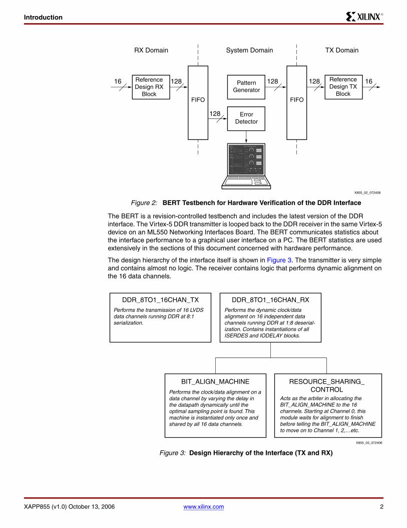
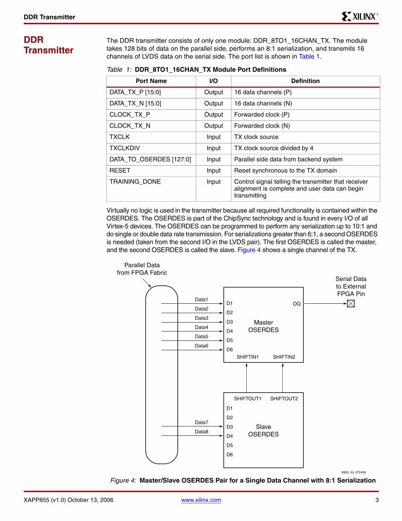
DDR Transmitter
XAPP855 (v10) October 13 2006 wwwxilinxcom 3
R
DDR Transmitter
The DDR transmitter consists of only one module DDR_8TO1_16CHAN_TX The module takes 128 bits of data on the parallel side performs an 81 serialization and transmits 16 channels of LVDS data on the serial side The port list is shown in Table 1
Virtually no logic is used in the transmitter because all required functionality is contained within the OSERDES The OSERDES is part of the ChipSync technology and is found in every IO of all Virtex-5 devices The OSERDES can be programmed to perform any serialization up to 101 and do single or double data rate transmission For serializations greater than 61 a second OSERDES is needed (taken from the second IO in the LVDS pair) The first OSERDES is called the master and the second OSERDES is called the slave Figure 4 shows a single channel of the TX
Table 1 DDR_8TO1_16CHAN_TX Module Port Definitions
Port Name IO Definition
DATA_TX_P [150] Output 16 data channels (P)
DATA_TX_N [150] Output 16 data channels (N)
CLOCK_TX_P Output Forwarded clock (P)
CLOCK_TX_N Output Forwarded clock (N)
TXCLK Input TX clock source
TXCLKDIV Input TX clock source divided by 4
DATA_TO_OSERDES [1270] Input Parallel side data from backend system
RESET Input Reset synchronous to the TX domain
TRAINING_DONE Input Control signal telling the transmitter that receiver alignment is complete and user data can begin transmitting
Figure 4 MasterSlave OSERDES Pair for a Single Data Channel with 81 Serialization
MasterOSERDES
Serial Datato ExternalFPGA Pin
X855_04_072406
Parallel Datafrom FPGA Fabric
SlaveOSERDES
SHIFTIN1 SHIFTIN2
SHIFTOUT1 SHIFTOUT2
OQD1
D2
D3
D4
D5
D6
D1
D2
D3
D4
D5
D6
Data1
Data2
Data3
Data4
Data5
Data6
Data7
Data8
DDR Transmitter
XAPP855 (v10) October 13 2006 wwwxilinxcom 4
R
The transmitter interface (Figure 5) consists of 16 masterslave OSERDES pairs like the one shown in Figure 4 page 3 Since this interface is source synchronous the clock must also be forwarded using the ODDR module
The only logic in the TX Interface is the multiplexer that selects between real data and the training pattern Since this interface depends on dynamic alignment within the receiver the transmitter is required to send a training pattern until the receiver completes the alignment process on all 16 channels In the design described in this application note the select line to that multiplexer is assumed to be connected to a feedback signal from the receiver interface If a feedback signal from the RX interface is undesirable the MUX select line can be tied to a
Figure 5 Block Diagram of TX Interface
MasterDATA_TX_P[00][50]
[76]
[138]
128128
128
128
[1514]
[125120]
[127126]
DATA_TX_N[00]
DATA_TX_P[01]
DATA_TX_N[01]
DATA_TX_P[15]
DATA_TO_OSERDES
TRAINING_PATTERN
ClockSource BUFR(divide4)
TXCLKDIV(1)
TXCLK(1)
BUFIO
DATA_TX_N[15]
QD
Slave
Master
OSERDES_CH_00 LVDSEXT_25
LVDSEXT_25
LVDSEXT_25
CLOCK_TX_P
CLOCK_TX_N
X855_05_072406
LVDSEXT_25
OSERDES_CH_01
TRAINING_DONE
OSERDES_CH_15
ODDR
Slave
Master
CLK Q
D1D2
10
Slave
Notes1 TXCLK and TXCLKDIV drive all OSERDES both master and slave
Interface Clocking
XAPP855 (v10) October 13 2006 wwwxilinxcom 5
R
timer that grants the receiver a fixed amount of time to complete alignment For example the transmitter can transmit the training pattern for 500 ms after which it assumes that the receiver alignment process is complete and sends real data
Table 2 shows the device utilization statistics for the TX interface implemented in a Virtex-5 device Since there is no combinatorial logic in the transmitter no look-up tables (LUTs) are used The 128-bit MUX is implemented using only 128 flip-flops and no combinatorial logic Table 2 also shows one BUFIO and one BUFR being used This design can also be implemented using two BUFGs and a DCM instead The different clocking options for this interface are discussed in ldquoInterface Clockingrdquo
Interface Clocking
In the block diagram of the DDR transmitter shown in Figure 5 page 4 the clock networks are shown driven by BUFIO and BUFR When BUFIO and BUFR are used to generate the serial and parallel clocks the phase relationship between the two clocks is guaranteed by design to meet the input requirements of the OSERDES (and ISERDES) Another valid way of driving the clock networks in Figure 5 is to use global clocks combined with a DCM to divide by four This scheme also provides phase-matched clock outputs guaranteed by design to meet the input requirements of the OSERDES The two valid clocking schemes are shown in Figure 6
Table 2 DDR TX Interface Utilization Statistics
Component Quantity Usage Description
Slice Flip-Flop 128 Registered MUX output of DATA_TO_OSERDES
Slice 32 1284 FFs per slice = 32 slices
LUT 0 ndash
IOB 34 17 LVDS output pairs (16 data 1 clock)
OSERDES 32 Master and slave OSERDES for every LVDS data pair
BUFIO 1 TXCLK
BUFR 1 TXCLKDIV
Figure 6 Global and Regional Clocking Schemes in Virtex-5 FPGAs
BUFR(divideX)
BUFIO
DIVI
OFB
CLKDIV
CLK
OSERDESISERDES
ClockInputGlobal
Scheme
ClockInputChipSync
Scheme
DCMBUFG BUFG
BUFG
CLKDIV
CLK
OSERDESISERDES
X855_06_072406
Interface Clocking
XAPP855 (v10) October 13 2006 wwwxilinxcom 6
R
Which clocking scheme is the best to use The BUFIOBUFR networks maximize performance at the expense of some convenience BUFIO and BUFR are regional clocks that cannot span the entire chip like a global clock This difference means that transferring data between the regional and global domains must be a part of the designers task and can simply mean adding a FIFO between the clock domains
Global clocks have lower performance than BUFIO but are more convenient to use If a clock is placed on a global network it can reach any component in the entire device To show the performance advantage of BUFIO Table 3 shows snapshots of several timing parameters some of which are included in the timing budget calculations for source synchronous interfaces In each case BUFIO has an advantage over BUFG and collectively those advantages are significant These parameters are used in the timing budget calculation section ldquoInterface Timing Budgetrdquo page 18 For the most current specifications always consult the data sheet on wwwxilinxcom
To offer the maximum performance the interface described in this application note uses a BUFIOBUFR clocking scheme in both the transmitter and receiver The interface does not include the FIFO logic necessary to transfer the parallel data tofrom the backend system domain However the BERT design discussed in ldquoIntroductionrdquo page 1 (see Figure 2 page 2) shows how to transfer data tofrom the RX and TX clock domains by using a FIFO18_36 primitive
Table 3 Comparison of Global and IO Clock Performance by Speed Grade
-3 -2 -1 Units
Maximum Frequency
BUFG max frequency 550 500 450 MHz
BUFIO max frequency 710 710 644 MHz
Duty Cycle Distortion
BUFG DYCD 150 150 150 ps
BUFIO DYCD 100 100 100 ps
Sampling Error
BUFG TSAMP 450 500 550 ps
BUFIO TSAMP 350 400 450 ps
Clock Tree Skew
BUFG skew for XC5VLX50T 270 270 270 ps
BUFIO skew for all devices 50 50 50 ps
DDR Receiver
XAPP855 (v10) October 13 2006 wwwxilinxcom 7
R
DDR Receiver The DDR receiver consists of three core modules DDR_8TO1_16CHAN_RX BIT_ALIGN_MACHINE and RESOURCE_SHARING_CONTROL The receiver is more complex than the DDR transmitter because it includes a dynamic alignment algorithm implemented in the FPGA fabric The DDR_8TO1_16CHAN_RX module takes 16 channels of data on the serial side optimizes the timing relationship of each channel with the clock performs 18 deserialization and presents 128 bits of data on the parallel side The port list is shown in Table 4
Table 4 DDR_8TO1_16CHAN_RX Module Port Definitions
Port Name IO Definition
DATA_RX_P [150] Input 16 data channels (P)
DATA_RX_N [150] Input 16 data channels (N)
CLOCK_RX_P Input Forwarded clock (P)
CLOCK_RX_N Input Forwarded clock (N)
INC_PAD Input Pulsing this pin causes the IDELAY tap setting of all data channels to increment by 1
DEC_PAD Input Pulsing this pin causes the IDELAY tap setting of all data channels to decrement by 1
DATA_FROM_ISERDES [1270] Output Parallel side data to backend system
RESET Input Reset synchronous to the RX domain
IDLY_RESET Input Reset synchronous to the RX domain that only resets the IDELAY tap settings of all data channels
IDELAYCTRL_RESET Input Reset synchronous to the TX domain that only resets the IDELAYCTRL module
BITSLIP_PAD Input Pulsing this pin causes one bitslip operation on all data channels
CLK200 Input Reference clock to IDELAYCTRL module
TAP_00 TAP_01 TAP_03 TAP_04 TAP_05 TAP_06 TAP_07 TAP_08 TAP_09 TAP_10 TAP_11 TAP_12 TAP_13 TAP_14 TAP_15
Output[50] Each of these 6-bit signals contains the current IDELAY tap value of the sixteen data channels Possible values 0-63
TAP_CLK [50] Output The 6-bit signal containing the current IDELAY tap value of the clock channel Permanently set to zero because the clock channel is not adjusted
TRAINING_DONE Output Flag indicating alignment is complete
RXCLK Output RX Source Sync Clock
RXCLKDIV Output RX Source Sync Clock divided by 4
IDELAY_READY Output Flag indicating IDELAYCTRL is calibrated
DDR Receiver
XAPP855 (v10) October 13 2006 wwwxilinxcom 8
R
Most of the logic used in the receiver is contained within the ISERDES The ISERDES is part of the ChipSync technology and is found in IO of all Virtex-5 devices The ISERDES can be programmed to do any deserialization up to 110 and do single or double data rate reception For deserializations greater than 61 a second ISERDES is needed (taken from the second IO in the LVDS pair) The first ISERDES is called the master and the second ISERDES is called the slave Figure 7 shows a single channel of the RX
Figure 7 MasterSlave ISERDES Pair for a Single Data Channel with 18 Deserialization
MasterISERDES
Serial DataExternal to
FPGA
X855_07_080306
Parallel Datainto FPGA Fabric
SlaveISERDES
SHIFTOUT2SHIFTOUT1
SHIFTIN2SHIFTIN1
Q1
Q2
Q3
Q4
Q5
Q6
Q1
Q2
Q3
Q4
Q5
Q6
Data8
Data7
Data6
Data5
Data4
Data3
Data2
Data1
DDR Receiver
XAPP855 (v10) October 13 2006 wwwxilinxcom 9
R
The receiver interface (Figure 8) consists of 16 masterslave ISERDES pairs Since this interface is source synchronous the clock source comes from the transmitter The clock is buffered in the receiver by a BUFIO component and divided to the parallel clock rate by a BUFR component
Figure 8 Block Diagram of RX Interface
MasterDATA_RX_P[00]
DATA_RX_N[00]
LVDS_25
Slave
IODELAY
CHAN_SELDATA_ALIGNED
DATA_TO_MACHINE
RXCLK(1)
START_ALIGN
Master
LVDS_25
Slave
ISERDES_CH_01 IODELAY
X855_08_082806
DQ
BUFIO
BUFR (divide4)
8 [72]
[10]
[98]
[1510]
[127122]
[121120]
4
8
8 8
3
3
3
DATA_RX_P[01]
DATA_RX_N[01]
Master
LVDS_25
Slave
IODELAY
DATA_RX_P[15]
DATA_RX_N[15]
ISERDES_CH_15
ISERDES_CH_00
RXCLKDIV
INC
ICE
BITSLIP
RXCLKDIV(1)
INC ICEBITSLIP
To CH 15
To CH 01
To CH 00
RX_IDELAYCTRL
Resource SharingControl
Bit AlignMachine
200 MHzSource
LVDS_25
CLOCK_RX_N
CLOCK_RX_P
Notes1 RXCLK and RXCLKDIV drive all ISERDES both master and slave
IODELAY
Fixed to Tap 0
Decoder
DDR Receiver
XAPP855 (v10) October 13 2006 wwwxilinxcom 10
R
Each ISERDES in Figure 8 page 9 contributes 8 bits to the 128-bit parallel data bus Since there is only one instance of BIT_ALIGN_MACHINE in the receiver each data channel must be aligned separately by sharing that resource The 8-bit data buses from each ISERDES are fed into a MUX which selects which of the 16 channels has access to the BIT_ALIGN_MACHINE resource RESOURCE_SHARING_CONTROL controls the MUX to ensure that every channel completes its alignment before the MUX switches to the next channel The START_ALIGN signal tells the BIT_ALIGN_MACHINE that alignment can begin on the current channel because the MUX output is stable The DATA_ALIGNED signal tells the RESOURCE_SHARING_CONTROL module that alignment on the current channel is complete
The order of the parallel data outputs of the ISERDES is the opposite of the parallel data inputs of the OSERDES The least significant OSERDES data inputs are fed into the master while the least-significant ISERDES data outputs come from the slave (Figure 4 page 3 versus Figure 7)
The IDELAYCTRL module in Figure 8 is shown as having no connection to the rest of the receiver Actually IDELAYCTRL is required to calibrate the IODELAY blocks in the path of each data channel A single IDELAYCTRL block is sufficient to calibrate all 16 data channels since all channels are in the same bank
The BIT_ALIGN_MACHINE generates three control signals that adjust the timing of the appropriate ISERDES INC and ICE cause the IODELAY to increment or decrement the delay in the datapath by a fixed amount of ~75 ps (if a 200 MHz reference clock is used) BITSLIP causes each ISERDES to rotate the order of the parallel output data bits facilitating the process of word alignment These three control signals are directed to the appropriate ISERDES by the decoder shown in Figure 8 Although not shown in the figure the decoder is also controlled by the RESOURCE_SHARING_CONTROL module
Table 5 shows the device utilization statistics for the RX interface implemented in a Virtex-5 device These figures exclude the counters used to track the IODELAY settings on all data channels in most instances those counters can be removed after the interface is integrated and verified in a specific environment The majority of the LUTs utilized are consumed by the BIT_ALIGN_MACHINE which is the core of the receiver alignment algorithm As in the TX interface the RX interface consumes one BUFIO and one BUFR for clocking The clocking could also be accomplished using BUFGs and a DCM as described in ldquoInterface Clockingrdquo page 5 but the performanceconvenience trade off would need to be considered
Table 5 DDR RX Interface Utilization Statistics
Component Quantity Usage Description
Slice Flip-Flop 131 Multiple uses
Slice 105 Multiple uses
LUT 263 Multiple uses
IOB 34 17 LVDS input pairs (16 data 1 clock)
ISERDES 32 Master and slave ISERDES for every LVDS data pair
BUFIO 1 RXCLK
BUFR 1 RXCLKDIV
Receiver Interface Dynamic Timing
XAPP855 (v10) October 13 2006 wwwxilinxcom 11
R
Receiver Interface Dynamic Timing
The timing of the receiver interface is broken into two parts
bull The suboptimal timing inherent in the data and clock paths
bull The optimal timing created by the receiver when adjusting dynamic delays on each of the 16 data channels
Inherent Timing
An inventory of all propagation delays in the clock and datapaths must be taken to derive the inherent setuphold times The clock and datapaths for a single channel of this interface are shown in Figure 9 The ISE Timing Analyzer breaks down the paths into the timing parameters shown All components in the path have both a minimum and maximum value to account for process variations
Figure 10 page 12 shows the timing analyzer settings used to generate the information in this report Each of the timing parameters is described in Table 6 page 12 and Table 7 The minimum and maximum values of the individual timing parameters for the clock and datapaths are shown in Table 8 and Table 9 page 13
Note All raw timing numbers referenced in this document are subject to minor changes in subsequent revisions of the ISE tools
Figure 9 Timing Components of RX Data and Clock Paths
ISERDESFFsIODELAY
VariableInit to 0
DI O
CLK
IODELAYIBUFDS
IBUFDS
+
ndash
+
ndash Fixed toTap 0
I O
X855_09_082806
DataPath
ClockPath
TIOPI TIODDO_IDATAINTNET1 TNET2
TIOPI TIODDO_IDATAIN TISDCK_DDLY
TBUFIOCKO_O
BUFIO
Receiver Interface Dynamic Timing
XAPP855 (v10) October 13 2006 wwwxilinxcom 12
R
Figure 10 ISE Timing Analyzer Properties Used in this Document
Table 6 Datapath Timing Definitions
Timing Parameter Description
TIOPI Delay from the IOB pad through the LVDS input buffer to the I pin of the IOB pad
TIODDO_IDATAIN Delay from the I pin of IOB pad to the D input of the ISERDES
TISDCK_DDLY Delay from the D input of the ISERDES to the sampling registers in the ISERDES (setup and hold times of ISERDES)
Table 7 Clock Path Timing Definitions
Timing Parameter Description
TIOPI Delay from the IOB pad through the LVDS input buffer to the I pin of the IOB pad
TIODDO_IDATAIN Delay from I pin of IOB pad to the O output of the IODELAY block
TNET1 Delay from the O output of the IODELAY block to the I pin of BUFIO
TBUFIOCKO_O Clock to out delay of BUFIO
TNET2 Clock distribution delay from BUFIO output to the clock input of data ISERDES
Table 8 Datapath Delay Inventory for a -1 Speed Grade XC5VLX50T Device
Timing Parameter Maximum Datapath Delay Minimum Datapath Delay
TIOPI 1083 ns 0763 ns
TIODDO_IDATAIN 0671 ns 0671 ns
TISDCK_DDLY 0064 ns ndash0038 ns
TOTAL 1818 ns 1396 ns
XAPP855_10_071306
Receiver Interface Dynamic Timing
XAPP855 (v10) October 13 2006 wwwxilinxcom 13
R
According to the inherent timing prediction the data is going to arrive before the clock by an amount determined by Equation 1 and Equation 2 Equation 1 calculates that data arrives before the clock by at least 1076 ns in a -1 device Equation 2 calculates that data arrives before the clock by at most 2213 ns Equation 3 shows a timing window that covers all -1 devices under all conditions This timing window describes the inherent timing of the data and clock paths Assuming skew-matched PCB traces for all sixteen channels then it can be assumed that all 16 channels in the receiver have roughly the same timing window
Equation 1
Equation 2
Equation 3
Figure 11 shows the timing windows for all speed grades of an XC5VLX50T device as well as a hardware measurement of the inherent timing relationship (to validate the calculations) The hardware measurement shows the DDR interface data arriving 1425 ns before the clock which by inspection places the device in all three speed grade ranges (the device used for the hardware measurement is a -2 device)
Table 9 Clock Path Delay Inventory for a -1 Speed Grade XC5VLX50T Device
Timing Parameter Maximum Clock Path Delay Minimum Clock Path Delay
TIOPI 1150 ns 0820 ns
TIODDO_IDATAIN 0671 ns 0671 ns
TNET1 0254 ns 0190 ns
TBUFIOCKO_O 1130 ns 0894 ns
TNET2 0404 ns 0319 ns
TOTAL 3609 ns 2894 ns
Setup Time Max Data Delay Min Clock Delay 1818 2894ndash 1076 nsndash==ndash=
Hold Time Max Clock Delay Min Data Delay 3609 1396ndash 2213 ns==ndash=
Timing Window 2213 1076ndash 1137 ns==
Figure 11 Timing Windows Show Uncertainty in ClockData Relationship as Calculated by Timing Analyzer
400 Mbs Data (T = 25 ns)
1425 ns Hardware MeasurementData Arrives
x855_11_091806
-11076ns 2213 ns
-21043 ns 2039 ns
-30989 ns 1878 ns
Receiver Interface Dynamic Timing
XAPP855 (v10) October 13 2006 wwwxilinxcom 14
R
Dynamic Timing and BIT_ALIGN_MACHINE
In ldquoInherent Timingrdquo page 11 the inherent timing of the interface was calculated for all speed grades and validated with a hardware measurement In that case the inherent timing was sufficient because the data rate is only 400 Mbs (Figure 11 page 13) What happens when the data rate is increased such that the hold edge of the data window begins to shrink (Figure 12)
At 600 Mbs the inherent timing relationship is no longer adequate to meet timing because there are cases when the sampling clock edge is in the middle of the data transition As the data rates increase to 800 and 1000 Mbs the clock actually captures the data arriving one bit time later For designs that are sensitive to word alignment this is unacceptable
The solution to the suboptimal inherent timing is dynamic timing The BIT_ALIGN_MACHINE module in the receiver performs two functions of dynamic timing
bull Bit Alignment Position the sampling edge of the clock at the center of the data eye by adding delay to the datapaths
bull Word Alignment Ensure that the parallel data bits are in the correct order at the output of the ISERDES by using the bitslip function in the ISERDES
The steps of the bit-alignment procedure are shown in Figure 13 page 15 Each step of the algorithm can either add or subtract delay from the datapath All 16 channels are taken through this procedure independently This procedure measures one full data eye (in terms of 75 ps delay taps) and then returns to the center of the data eye Steps 1 and 2 are dedicated to moving through the partial eye of the initial timing while steps 3 and 4 are dedicated to measuring a full eye Step 5 is dedicated to positioning the clock edge at the center of the data eye
Figure 12 Inherent Timing Windows Shown in Relation to Multiple Data Rates
400 Mbs Data (T = 25 ns)
600 Mbs Data (T = 167 ns)
800 Mbs Data (T = 127 ns)
1000 Mbs Data (T = 10 ns)
-11076ns 2213 ns
-21043 ns 2039 ns
-30989 ns
1425 ns
1878 ns
Hardware MeasurementData Arrives
x855_12_091806
Receiver Interface Dynamic Timing
XAPP855 (v10) October 13 2006 wwwxilinxcom 15
R
Jitter is represented in Figure 13 as multiple transition lines Accounting for jitter is a crucial part of the algorithm In step 2 the first data transition is found If there is no jitter then the eye measurement can begin instantly after finding the transition However when jitter is considered the algorithm must find the first transition move through the transition and then begin looking for the second transition If the algorithm does not move through the first transition intelligently it runs the risk of falsely detecting the second transition
Once bit alignment is complete the order of the data bits can be adjusted to achieve word alignment The bit-alignment procedure ensures that data is being sampled correctly but the order of the data can be a few bits off from where the receiver expects it to be To correct this the bitslip feature of the ISERDES is used to slip bit times until the proper alignment is found For this feature to be useful a training pattern must be generated by the transmitter (as discussed in ldquoDDR Transmitterrdquo page 3) that the receiver can use to determine the proper word alignment In this reference design the training pattern is 00101100 (0x2C) This pattern is mostly arbitrary as many other patterns work just as well This pattern was chosen because a training pattern should behave electrically as much like real data as possible such that the center of the training eye is the center of the data eye Since real data contains strings of consecutive ones and zeros it is best for the training pattern to do the same For that reason a 0x2C pattern is better than an 0xAA pattern because it contains run lengths of 1 2 3 and 4 bit times
Table 10 page 16 shows the word-alignment process in the case where bit alignment completes with the data outputs set to 0x58 Since 0x58 is not the training pattern the receiver is looking for bitslip is asserted until 0x2C is found This reference design uses a 18 deserialization so there are only eight possible configurations of the parallel data outputs If bitslip is asserted infinitely the same eight configurations will repeat Bitslip in DDR mode is somewhat irregular because it does not simply rotate by one bit on every bitslip cycle This effect is inconsequential to the word-alignment procedure (see the Virtex-5 User Guide for more details)
Figure 13 Dynamic Bit-Alignment Procedure in BIT_ALIGN_MACHINE
Data 0
Data Arrives Before Clock
Data 1
x855_13_091806
Data 0 Data 1
Data 0 Data 1
Data 0 Data 1
Data 0 Data 1
Sampling Clock (Fixed Delay)
Return to Center of Eye
End Measuring Eye
Begin Measuring Eye
Find 1st Transition
Initial Timing1
2
3
4
5
Receiver Interface Dynamic Timing
XAPP855 (v10) October 13 2006 wwwxilinxcom 16
R
The FSM in the BIT_ALIGN_MACHINE module used to implement both bit and word alignment is shown in Figure 14 page 17 The FSM is divided into five sections loosely described as finding the first transition getting through the first transition finding the second transition returning to the center of the eye and word alignment
To get through the first transition effectively for all possible types of jitter two methods are used The first method pertains to random jitter If there is a lot of random jitter at the sampling point then the samples generated are not stable The algorithm detects this instability by comparing current samples to older samples and therefore knows where the transition begins and ends But what if the jitter is extremely deterministic The transition then has discreet crossing points such that within the transition there is very stable but incorrect data In this case the algorithm does not sense any instability and falsely concludes that the sampling point is not in the transition To address this case apart from evaluating stability the algorithm also evaluates the correctness of the data content by using the bitslip feature in the middle of the transition For example if the algorithm determines that the sampled data is stable it then asserts bitslip to look for the correct data If 0x2c is found within eight assertions of bitslip then the sampling point is not in the transition But if 0x2c is not found then the algorithm increments the data delay and repeats the transition test again
Table 10 Word Alignment in the DDR Receiver
Bitslip Cycle Data Value (Hex) Data Value (Bin) Description of Bitslip operation
1 58 0101 1000 ndash
2 0B 0000 1011 Rotate 3 bits to right
3 16 0001 0110 Rotate 1 bit to left
4 C2 1100 0010 Rotate 3 bits to right
5 85 1000 0101 Rotate 1 bit to left
6 B0 1011 0000 Rotate 3 bits to right
7 61 0110 0001 Rotate 1 bit to left
8 2C 0010 1100 Rotate 3 bits to right
Receiver Interface Dynamic Timing
XAPP855 (v10) October 13 2006 wwwxilinxcom 17
R
Figure 14 FSM in the BIT_ALIGN_MACHINE Module
TRANSITION_CHECK (01000)
First TransitionNot Detected
First TransitionNot Detected
First TransitionDetected
First TransitionDetected
Past the FirstTransition
Second TransitionNot Detected
Second TransitionDetected
Decrement DelayAgain
Bit AlignmentComplete
Still Samplingin Transition
INC_ONCE (01111)
SEARCH_PAT (01101)
IDLE (01100)
IDLE (10000)
RECHECK_TRANS (00010)
ONE_BITSLIP (00110)
INC_ONCE (01011)
WAIT_8_CYCLES (00100)
COUNT_1 (01110)
INC_ONCE (01001)
WAIT_8_CYCLES (00011)
IDLE (10010)
TRAINING_DONE (00111)
FIRST_SAMPLE (00001)
RESET (00000)
DEC_TO_HALF (01010)
WORD_ALIGN (00101)
X855_14_082806
Routine to Avoid False Detection of Second Transition
=CHECK_PATTERN
Receiver Interface Dynamic Timing
XAPP855 (v10) October 13 2006 wwwxilinxcom 18
R
Interface Timing Budget
In addition to sampling the data as closely as possible to the center of the data eye the actual size of the data eye is important By accurately predicting the size of the data eye in the receiver the overall performance ceiling of the interface can be inferred The ideal data eye width is the period of the data rate (for example TBit_Period = 100 ns for 1000 Mbs) Both the transmitter and receiver circuits have sources of error that subtract from the ideal data eye The equation for the eye width at the output of the transmitter is shown in Equation 4 TJITTER is the peak-to-peak jitter of the clock source driving the transmitter data bus and forwarded clock TDCD is the maximum duty cycle distortion of the clock tree driving the data bus and forwarded clock Skew is not considered in the transmitter or receiver because the receiver calibrates out skew between channels by performing alignment on each channel individually
Equation 4
Equation 5 calculates the width of the data eye at the receiver flip-flops Ideally the eye width at the receiver is the same as the eye width at the output of the transmitter but there are sources of error in the transmission medium and receiver circuitry Duty cycle distortion must be considered again on the receiver clock tree TSAMP_BUFIO is the receiver sampling error due to drift caused by voltage and temperature variations TIDELAYPAT_JIT is the amount of pattern dependent jitter that is accumulated in each tap of the IDELAY chain For a clock pattern TIDELAYPAT_JIT is 0 pstap peak to peak For a data pattern with long and short run lengths of zeroes and ones (simulated by PRBS23) TIDELAYPAT_JIT is a finite value that must be considered in the timing budget
Equation 5
TBOARD_JITTER includes jitter induced by receiver input capacitance and the parasitics of the physical data path on the PCB TBOARD_JITTER must be determined by simulation as it varies as a function of frequency and for receivers of different types and vendors On the ML550 with a -2 speed-grade Virtex-5 device the TBOARD_JITTER is measured at roughly 200 ps at 900 Mbs (assuming data content equivalent to PRBS23) TQUANTIZATION_ERR or quantization error is caused by the granularity of the IDELAY tap chain Working with 75 ps increments it is not possible to utilize the entire data eye since inevitably some valid eye width is lost between two taps The value for this loss is 75 ps As long as the receiver eye width calculated using Equation 5 is greater than or equal to 0 the interface operates correctly over process voltage and temperature
For example Equation 6 and Equation 7 show the timing budget calculation for the DDR interface running at 900 Mbs in a -2 speed grade device on an ML550 evaluation board Refer to the data sheet for the most current values The TX interface is looped back to the RX interface on the same Virtex-5 FPGA as shown in Equation 2
Equation 6
Equation 7
Changes in voltage and temperature cause the data channels of the interface to drift relative to the clock If the DDR interface were to transfer user data for a long period of time over all specified conditions of temperature and voltage Equation 7 states that there would be at least 107 ps (one or two IDELAY taps) of data window remaining valid during all fluctuations of temperature and voltage Compare this calculation to the measurements in Table 12 page 21 Case 900 Mbs There are four taps that are error free under all conditions In ldquoAppendixrdquo there are three -2 devices tested at 900 Mbs and each has 4 4 and 3 taps respectively that are error free under all conditions
DATA_EYE_WIDTH_TX TBIT_PERIOD TJITTERndash TDCD_BUFIOndash=
DATA_EYE_WIDTH_RX DATA_EYE_WIDTH_TX
TBOARD_JITTER
ndash
TSAMP_BUFIOndash TDCD_BUFIOndash
TIDELAYPAT_JIT IDELAY taps in datapathtimes[ ]ndash
TQUANTIZATION_ERRndash
=
DATA_EYE_WIDTH_TX 1111 ps 25 psndash 100 psndash 986 ps= =
DATA_EYE_WIDTH_RX986 ps 200 psndash 400 psndash 100 psndash 8 ps 13 tapstimes[ ] 75 ps 107 ps=ndashndash
=
Interface Characterization
XAPP855 (v10) October 13 2006 wwwxilinxcom 19
R
At a given temperature and voltage setting the data valid window is much larger because there is no drift when temperature and voltage are constant The size of the data valid window under constant conditions is 107 ps + TSAMP_BUFIO which in this case is at least 507 ps (six or seven IDELAY taps) Compare this calculation to the measurements of any single condition in Table 12 Case 900 Mbs In the worst case (ndash5 supply) there are 7 taps that are error free
Equation 8 and Equation 9 show the same timing budget calculation for the DDR interface running at 10 Gbs in a -2 speed grade device on an ML550 Evaluation Board
Equation 8
Equation 9
Equation 9 predicts that no data window remains valid during all specified fluctuations of temperature and voltage (compare to Table 12 Case 1000 Mbs) In ldquoAppendixrdquo there are three -2 devices tested at 1000 Mbs and each has 1 3 and 1 taps respectively that are error free under all conditions This data rate and device combination are very marginal cases
To operate at 10 Gbs the DDR interface requires additional circuitry to track out voltage-temperature variations in real-time (see XAPP860 16-channel DDR LVDS Interface with Real-time Window Monitoring for a DDR Interface with real-time window monitoring) If the voltage-temperature variations are removed from the picture the predicted data valid window is ndash120 ps + TSAMP_BUFIO which in this case is at least 280 ps (3 or 4 taps) Compare this calculation to the measurements of any single condition in Table 18 page 34 There are at least four error-free taps in all conditions
Interface Characterization
By following the procedure illustrated in Figure 13 page 15 the bit-alignment algorithm should never insert more than approximately 15 bit times of delay on the data channels The fewest number of delay taps should be used in the datapath because they produce a finite amount of degradation (TIDELAYPAT_JIT) The worst-case initial timing for the algorithm occurs when the clock samples just before the data transitions as in the 600 Mbs case in Figure 12 page 14 The algorithm must move all the way through the first eye to find the first transition (1 bit time) and then move halfway into the next eye to center the sampling point (05 bit time) This process produces a worst-case total delay insertion of 15 bit times
The actual performance of the bit-alignment algorithm is characterized as a function of data rate in Figure 15 page 20 For all data rates the expectation is that the tap settings of all 16 channels in the DDR receiver do not exceed approximately 15 bit times of delay Both the maximum and minimum tap setting of all 16 channels is recorded for each data rate This graph only shows the data for a single device Comparing the 15 bit time mask to the actual settings it is clear that the algorithm remains within the 15 bit time limit At 13 Gbs the tap setting actually exceeds the mask by one tap (a negligible violation)
DATA_EYE_WIDTH_TX 1000 ps 25 psndash 100 psndash 875 ps= =
DATA_EYE_WIDTH_RX 875 ps 300 psndash400 ps 100 psndash
ndash8 ps 15 tapstimes[ ] 75 ps 120 psndash=ndashndash
=
Interface Characterization
XAPP855 (v10) October 13 2006 wwwxilinxcom 20
R
The maximum and minimum tap settings in Figure 15 generally stay within 3 to 4 taps of each other except in the case of 640 Mbs and 1300 Mbs data rates These data rates are seams in the inherent timing At data rates below 640 Mbs the tap settings are in the range of 30 taps and at data rates above 640 Mbs the tap settings are in the range of 12 taps Referring back to Figure 12 page 14 it is clear why this seam occurs As the data rate increases past 600 Mbs the initial sampling point of the inherent timing moves into a different data eye creating a different starting point for the algorithm At 640 Mbs some of the 16 channels start in one eye while other channels start in the other eye Fortunately this is not an issue because the single bit time of difference between the channels is resolved using bitslip
Referring back to Figure 8 page 9 the clock channel goes through an IDELAY block with a default value of 0 Once the data rate is chosen for a given design this initial IDELAY value can be changed to a non-zero value to achieve more favorable inherent timing For example a design running at 620 Mbs can use 30 IDELAY taps on the delay channels each contributing a certain amount of jitter to the timing budget calculation By setting the initial clock delay to 5 taps the inherent timing moves across the seam shown in the 600 Mbs range of Figure 15 causing the data channels to only use about 12 IDELAY taps Only spectrally rich data patterns accumulate jitter in the IDELAY tap chain so the clock IDELAY can be set to any value without diminishing the timing budget This optimization is entirely optional and can be done once the design is running in hardware
The DDR receiver is designed to remove skew between channels by aligning each channel individually The ML550 board on which this reference design is characterized is designed to have minimal skew between channels However there is clearly a finite amount of skew between channels due to clock skew in the TX and RX BUFIO networks package skew and trace length tolerance on the ML550 board Table 11 page 21 shows how the bit-alignment algorithm sets the delay for each channel differently to compensate for skew between channels The table captures the range of settings among the 16 channels at specific data rates for a -2 device If there were additional skew among the 16 channels then the tap setting range would be larger to compensate for it The algorithm is designed such that skew between channels should not diminish the performance of the interface The range of tap settings differs for different devices and speed grades but the magnitude should be approximately the same
Figure 15 Bit-Alignment Algorithm Performance
60
50
40
30
20
10
0200 400 600 800 1000 1200 1400 1600
Data Rate (Mbs)
Del
ay T
ap U
tiliz
atio
n HW Measurement (Min)HW Measurement (Max)15 Bit Time Mask
X855_15_072406
Interface Characterization
XAPP855 (v10) October 13 2006 wwwxilinxcom 21
R
Since the receiver alignment logic only runs once immediately after reset the resulting dynamic timing must be adequate to ensure error-free operation over the specified voltage and temperature variations that can occur over time The data-valid window at the receiver input must be wide enough to withstand these variations (receiver drift) Table 12 page 21 shows the data-valid window at the ISERDES registers in the DDR receiver The eyes shown are collective eyes of all 16 channels The BERT testbench configuration loops back the DDR transmitter to the DDR receiver Using pattern generators and error detectors programmed to send and receive a pseudorandom bit sequence (PRBS23) the width of the data-valid window is evaluated using pseudorandom data that closely resembles real user data
Table 11 Tap Setting Range For Various Data Rates Measured on a -2 Device
Data Rate (Mbs) Tap Setting Range Compensated Skew
500 31ndash34 4 taps
600 28ndash30 3 taps
700 10ndash12 3 taps
800 11ndash13 3 taps
900 11ndash13 3 taps
1000 13ndash15 3 taps
1100 13ndash15 3 taps
1200 14ndash15 2 taps
Table 12 Measurement of Receiver Drift under Extreme Conditions for Multiple Data Rates
ConditionIODELAY Taps (1)
ndash8 ndash7 ndash6 ndash5 ndash4 ndash3 ndash2 ndash1 0 +1 +2 +3 +4 +5 +6 +7 +8
Case 800 Mbs
25degC Nom Supplies F F F P P P P P C P P P P P F F F
0degC Nom Supplies F F F P P P P P P P P P P P F F F
85degC Nom Supplies F F F P P P P P P P P P P P F F F
25degC +5 Supplies F P P P P P P P P P P P F F F F F
0degC +5 Supplies F P P P P P P P P P P P F F F F F
85degC +5 Supplies F P P P P P P P P P P P F F F F F
25degC ndash5 Supplies F F F F F F P P P P P P P P P F F
0degC ndash5 Supplies F F F F F F P P P P P P P P P P F
85degC ndash5 Supplies F F F F F P P P P P P P P P P F F
CONCLUSION Error free under all conditions when calibrated under nominal conditions to position C
Interface Characterization
XAPP855 (v10) October 13 2006 wwwxilinxcom 22
R
Case 900 Mbs
25degC Nom Supplies F F F F P P P P C P P P P F F F F
0degC Nom Supplies F F F F P P P P P P P P P F F F F
85degC Nom Supplies F F F F P P P P P P P P F F F F F
25degC +5 Supplies F F P P P P P P P P P F F F F F F
0degC +5 Supplies F F P P P P P P P P P F F F F F F
85degC +5 Supplies F F P P P P P P P P P F F F F F F
25degC ndash5 Supplies F F F F F F F P P P P P P P P F F
0degC ndash5 Supplies F F F F F F F P P P P P P P P F F
85degC ndash5 Supplies F F F F F F F P P P P P P P F F F
CONCLUSION Error free under all conditions when calibrated under nominal conditions to position C
Case 1000 Mbs
25degC Nom Supplies F F F F F P P P C P P P F F F F F
0degC Nom Supplies F F F F F P P P P P P P F F F F F
85degC Nom Supplies F F F F F P P P P P P P F F F F F
25degC +5 Supplies F F F P P P P P P P F F F F F F F
0degC +5 Supplies F F F P P P P P P P F F F F F F F
85degC +5 Supplies F F F P P P P P P P P F F F F F F
25degC ndash5 Supplies F F F F F F F F P P P P P P F F F
0degC ndash5 Supplies F F F F F F F F P P P P P P F F F
85degC ndash5 Supplies F F F F F F F F P P P P P P F F F
CONCLUSION Error free under all conditions when calibrated under nominal conditions to position C
Case 1100 Mbs
25degC Nom Supplies F F F F F P P P C P F F F F F F F
0degC Nom Supplies F F F F F P P P P P F F F F F F F
85degC Nom Supplies F F F F F P P P P P F F F F F F F
25degC +5 Supplies F F F P P P P P P F F F F F F F F
0degC +5 Supplies F F F P P P P P P F F F F F F F F
85degC +5 Supplies F F F P P P P P P F F F F F F F F
25degC ndash5 Supplies F F F F F F F F P P P P F F F F F
0degC ndash5 Supplies F F F F F F F F P P P P F F F F F
85degC ndash5 Supplies F F F F F F F F P P P P F F F F F
CONCLUSION Error free under all conditions when calibrated under nominal conditions to position C
Table 12 Measurement of Receiver Drift under Extreme Conditions for Multiple Data Rates (Continued)
ConditionIODELAY Taps (1)
ndash8 ndash7 ndash6 ndash5 ndash4 ndash3 ndash2 ndash1 0 +1 +2 +3 +4 +5 +6 +7 +8
Interface Characterization
XAPP855 (v10) October 13 2006 wwwxilinxcom 23
R
In all test cases shown in Table 12 page 21 the bit-align machine accurately places the sampling point in the center of the data eye (indicated by the C in each test case) In the 1100 Mbs case the bit-align machine places the sampling point slightly off center This slight inaccuracy occurs when the center of a real data pattern diverges from the center of the training pattern The electrical behavior of different data patterns is discussed below
After the dynamic timing is established for a given test case under nominal conditions the device is subjected to extremes of temperature and voltage to stress the receiver timing At data rates of 1100 Mbs and below the dynamic timing established after reset under nominal conditions is sufficient to meet timing over all specified extreme conditions (the column with the C passes traffic error free under all conditions) At a data rate of 1200 Mbs the design operates correctly under nominal conditions but the data-valid window is not large enough to withstand the voltage variations For this particular transmission medium the 1200 Mbs case requires a real-time adjustment circuit that could track the center of the eye
The full datapath of the testbench consists of
TX rarr 5 FR-4 rarr SAMTEC QSE Conn rarr 12 Ribbon Cable rarr SAMTEC QSE Conn rarr 5 FR-4 rarr RX
For shorter transmission media higher performance can be achieved in accordance with the section ldquoInterface Timing Budgetrdquo page 18 Interface performance is not solely a question of the LVDS driver performance specification but rather a question of adequate timing margin to withstand production and environmental variations From Table 12 the total amount of variation experienced over temperature and voltage is roughly 375 ps (5 taps at 75 ps per tap) This number should be comparable to the specification for receiver sampling error (TSAMP_BUFIO) shown in the Virtex-5 Data Sheet
Case 1200 Mbs
25degC Nom Supplies F F F F F F P P C P F F F F F F F
0degC Nom Supplies F F F F F F P P P P F F F F F F F
85degC Nom Supplies F F F F F F P P P F F F F F F F F
25degC +5 Supplies F F F F P P P P F F F F F F F F F
0degC +5 Supplies F F F P P P P P F F F F F F F F F
85degC +5 Supplies F F F F P P P P F F F F F F F F F
25degC ndash5 Supplies F F F F F F F F F P P P F F F F F
0degC ndash5 Supplies F F F F F F F F F P P P F F F F F
85degC ndash5 Supplies F F F F F F F F F P P F F F F F F
CONCLUSION Errors caused by plusmn5 variations in supply voltages
Notes 1 Where 0 is the reference tap determined by the bit-align machine under nominal conditions at 25degC2 P = Error-free transmission F = Error in transmission C = IODELAY tap position selected by bit-align machine under nominal conditions at 25degC3 Device under test is -2 speed grade
Table 12 Measurement of Receiver Drift under Extreme Conditions for Multiple Data Rates (Continued)
ConditionIODELAY Taps (1)
ndash8 ndash7 ndash6 ndash5 ndash4 ndash3 ndash2 ndash1 0 +1 +2 +3 +4 +5 +6 +7 +8
Interface Characterization
XAPP855 (v10) October 13 2006 wwwxilinxcom 24
R
Pattern Dependence of Receiver Performance
Different types of data patterns have different electrical signatures (rise and fall times jitter eye symmetry etc) A pattern with very narrow spectral content (such as a clock pattern) moves very favorably through the link because the receiver frequency response has little effect on the signal integrity However a pattern with wide spectral content (such as real data and pseudorandom patterns) stresses the links frequency response If the frequency response is not flat across the entire spectrum of the data content then the signal integrity is degraded as a result The amount of degradation measured is shown in Table 13 page 25 The DDR transmitter is looped back to the DDR receiver and different patterns are programmed to traverse the link Performance is assessed by evaluating the integrity of those patterns in the receiver
PRBS7 is a pseudorandom data pattern with a maximum run length of seven consecutive zeroes or ones PRBS15 is defined as having a maximum run length of fifteen consecutive zeroes or ones These limitations on run lengths limit the spectral content of the pattern A PRBS15 pattern has greater spectral content than a PRBS7 pattern and therefore is a more strenuous test for the link PRBS29 is the most strenuous test in Table 13 A clock pattern is effectively a PRBS1
As predicted Table 13 shows that there is more degradation for data patterns with more spectral content At 1000 Mbs and below the data eye closure is symmetrical Symmetrical eye closure is desired because it does not change the center of the eye as determined by the bit-alignment algorithm Above 1000 Mbs the eye closure becomes more asymmetrical causing the center of the data eye to diverge from the calibrated center (by only 1 tap)
In every data rate shown in Table 13 all significant pattern-dependent degradation is caused between PRBS1 (clock pat) and PRBS15 Between PRBS15 and PRBS29 there is no additional degradation recorded in any of the measurements
Interface Characterization
XAPP855 (v10) October 13 2006 wwwxilinxcom 25
R
Table 13 Link Performance for Various Types of Data Measured on a -2 Device
PatternIODELAY Taps (1)
ndash8 ndash7 ndash6 ndash5 ndash4 ndash3 ndash2 ndash1 0 +1 +2 +3 +4 +5 +6 +7 +8 +9
Case 600 Mbs
Clock Pat (0101) P P P P P P P P C P P P P P P P P P
Training Pat (0x2C) P P P P P P P P C P P P P P P P P F
PRBS7 P P P P P P P P C P P P P P P P P F
PRBS15 F P P P P P P P C P P P P P P P F F
PRBS23 F P P P P P P P C P P P P P P P F F
PRBS29 F P P P P P P P C P P P P P P P F F
Case 800 Mbs
Clock Pat (0101) F F P P P P P P C P P P P P P F F F
Training Pat (0x2C) F F P P P P P P C P P P P P P F F F
PRBS7 F F P P P P P P C P P P P P F F F F
PRBS15 F F F P P P P P C P P P P P F F F F
PRBS23 F F F P P P P P C P P P P P F F F F
PRBS29 F F F P P P P P C P P P P P F F F F
Case 1000 Mbs
Clock Pat (0101) F F F P P P P P C P P P P P F F F F
Training Pat (0x2C) F F F P P P P P C P P P P F F F F F
PRBS7 F F F F P P P P C P P P F F F F F F
PRBS15 F F F F F P P P C P P P F F F F F F
PRBS23 F F F F F P P P C P P P F F F F F F
PRBS29 F F F F F P P P C P P P F F F F F F
Case 1200 Mbs
Clock Pat (0101) F F F F P P P P C P P P P F F F F F
Training Pat (0x2C) F F F F P P P P C P P P F F F F F F
PRBS7 F F F F F P P P C P F F F F F F F F
PRBS15 F F F F F F P P C F F F F F F F F F
PRBS23 F F F F F F P P C F F F F F F F F F
PRBS29 F F F F F F P P C F F F F F F F F F
Case 1400 Mbs
Clock Pat (0101) F F F F F F P P C P P P F F F F F F
Training Pat (0x2C) F F F F F P P P C P P F F F F F F F
PRBS7 F F F F F F F P C P F F F F F F F F
PRBS15 F F F F F F F P C F F F F F F F F F
PRBS23 F F F F F F F P C F F F F F F F F F
PRBS29 F F F F F F F P C F F F F F F F F F
Notes 1 Where 0 is the reference tap determined by the bit-align machine under nominal conditions at 25degC2 P = Error-free transmission F = Error in transmission C = IODELAY tap position selected by bit-align machine under nominal conditions at 25degC
Resetting the Interface
XAPP855 (v10) October 13 2006 wwwxilinxcom 26
R
Resetting the Interface
Several dependencies determine the order in which circuits should be reset in the interface The receiver cannot begin the alignment algorithm if the transmitter is not sending the training pattern The transmitter must be reset before the receiver and time must be allowed for the training pattern to propagate across the link before the receiver comes out of reset The receiver also cannot begin the alignment algorithm until IDELAYCTRL has recovered from reset which could takes hundreds of cycles The recommended reset timing for the interface is shown in Figure 16 This reset timing is implemented in the BERT testbench for this interface
The TX reset (RST_TX) is used to reset all TX circuitry and also IDELAYCTRL The IDELAYCTRL reset is asynchronous so driving it with RST_TX is acceptable The minimum pulse width of IDELAYCTRL reset is 50 ns (TIDELAYCTRL_RPW) For that reason resets are held High for 16 clock cycles The RX reset (RST_RX) is used to reset all RX circuitry and is asserted when the IDELAYCTRL READY flag goes High indicating that the IODELAY blocks are calibrated
The timing of the READY flag in Figure 16 is a potential hazard Most likely it is High during a TX reset because it takes many cycles for IDELAYCTRL to deassert the READY flag It is easy to make the mistake of resetting the receiver too early To avoid this hazard the RX reset should be asserted only after seeing a deassertion and reassertion of the READY flag
Conclusion Based on the design and characterization described in this document the 16-Channel DDR reference design operates to the performance targets in Table 14 under all conditions of process voltage and temperature However to meet these targets over voltage and temperature the timing budget must be guaranteed according to the analysis in ldquoInterface Timing Budgetrdquo See ldquoAppendixrdquo page 27 for further justification of the maximum performance recommendations in Table 14
Figure 16 Recommended Interface Reset Timing
RST_TX
IDELAYCTRLREADY
RST_RX
16 Cycles X855_16_072406
Table 14 Performance of 16-Channel DDR Interface
Speed Grade Maximum Performance
-1 800 Mbs
-2 900 Mbs
-3 10 Gbs(1)
Notes 1 To achieve higher performance (up to 125 Gbs) see 16-channel DDR LVDS Interface with Realtime
Window Monitoring for an example of a DDR interface with real-time window monitoring
Appendix
XAPP855 (v10) October 13 2006 wwwxilinxcom 27
R
Appendix Performance Characterization Data
Refer to ldquoInterface Characterizationrdquo page 19 for explanations about how to interpret the data in the ldquoAppendixrdquo These tables show collective data eyes for the entire interface over process voltage and temperature (PVT) Three devices from each speed grade were selected for this characterization
The calibrated center position of the eye (marked by the C in the tables below) varies slightly from channel to channel (due to small skews between channels) That range is referred to as center tap range Analysis of Table 16 page 28 through Table 20 page 40 shows that the center tap range for slow and fast parts differ significantly at the same data rate (because the BIT_ALIGN_MACHINE algorithm adjusts for differences in speed)
All data in the ldquoAppendixrdquo is collected using the BERT testbench shown in Figure 2 page 2 The data pattern is PRBS23 and the devicepackage is XC5VLX50T-FF1136 The transmission path for the cases shown in Table 16 through Table 20 is repeated for convenience
TX rarr 5 FR-4 rarr SAMTEC QSE Conn rarr 12 Ribbon Cable rarr SAMTEC QSE Conn rarr 5 FR-4 rarr RX
A summary of these characterization results is shown in Table 15 Each of the nine parts were tested at 800 900 1000 1100 and 1200 Mbs When the interface is error free on all channels under all extreme conditions of temperature and voltage the particular test case is designated by a P A test case is marked FAIL when the interface suffered errors on any channel under any particular condition of voltage and temperature
Table 15 Summary of Interface Characterization Results
Device (SN) Speed Grade 800 Mbs 900 Mbs 1000Mbs 1100 Mbs 1200 Mbs
2194 -1 P P P FAIL FAIL
2219 -1 P FAIL FAIL FAIL FAIL
2199 -1 P P FAIL FAIL FAIL
001 -2 P P FAIL P FAIL
002 -2 P P P P FAIL
003 -2 P P FAIL FAIL FAIL
004 -3 P P P P P
005 -3 P P P P P
006 -3 P P P P P
Appendix
XAPP855 (v10) October 13 2006 wwwxilinxcom 28
R
Table 16 Measurement of Receiver Drift under Extreme Conditions at 800 Mbs
ConditionIODELAY Taps (1)
ndash8 ndash7 ndash6 ndash5 ndash4 ndash3 ndash2 ndash1 0 +1 +2 +3 +4 +5 +6 +7 +8
SN 2194 Speed Grade -1
25degC Nom Supplies F F F P P P P P C P P P P F F F F
0degC Nom Supplies F F F P P P P P P P P P P F F F F
85degC Nom Supplies F F F F P P P P P P P P P F F F F
25degC +5 Supplies F F P P P P P P P P P P F F F F F
0degC +5 Supplies F F P P P P P P P P P P F F F F F
85degC +5 Supplies F F P P P P P P P P P P F F F F F
25degC ndash5 Supplies F F F F F F P P P P P P P P P F F
0degC ndash5 Supplies F F F F F F P P P P P P P P P F F
85degC ndash5 Supplies F F F F F F P P P P P P P P P F F
Center Tap Range Taps 11ndash12
CONCLUSION Error free under all conditions when calibrated under nominal conditions to position C
SN 2219 Speed Grade -1
25degC Nom Supplies F F F P P P P P C P P P F F F F F
0degC Nom Supplies F F F P P P P P P P P P F F F F F
85degC Nom Supplies F F F P P P P P P P P P F F F F F
25degC +5 Supplies F P P P P P P P P P P F F F F F F
0degC +5 Supplies F P P P P P P P P P P F F F F F F
85degC +5 Supplies F P P P P P P P P P P F F F F F F
25degC ndash5 Supplies F F F F F F P P P P P P P P F F F
0degC ndash5 Supplies F F F F F F F P P P P P P P F F F
85degC ndash5 Supplies F F F F F F P P P P P P P P F F F
Center Tap Range Taps 13ndash16
CONCLUSION Error free under all conditions when calibrated under nominal conditions to position C
SN 2199 Speed Grade -1
25degC Nom Supplies F F F P P P P P C P P P P F F F F
0degC Nom Supplies F F F P P P P P P P P P P F F F F
85degC Nom Supplies F F F P P P P P P P P P P F F F F
25degC +5 Supplies F P P P P P P P P P P P F F F F F
0degC +5 Supplies F P P P P P P P P P P P F F F F F
85degC +5 Supplies F P P P P P P P P P P P F F F F F
25degC ndash5 Supplies F F F F F F P P P P P P P P P F F
0degC ndash5 Supplies F F F F F F P P P P P P P P P F F
85degC ndash5 Supplies F F F F F F P P P P P P P P P F F
Center Tap Range Taps 10ndash12
CONCLUSION Error free under all conditions when calibrated under nominal conditions to position C
Appendix
XAPP855 (v10) October 13 2006 wwwxilinxcom 29
R
SN 001 Speed Grade -2
25degC Nom Supplies F F F P P P P P C P P P P F F F F
0degC Nom Supplies F F F P P P P P P P P P P F F F F
85degC Nom Supplies F F F P P P P P P P P P P F F F F
25degC +5 Supplies F P P P P P P P P P P P F F F F F
0degC +5 Supplies F P P P P P P P P P P F F F F F F
85degC +5 Supplies F P P P P P P P P P P P F F F F F
25degC ndash5 Supplies F F F F F P P P P P P P P P P F F
0degC ndash5 Supplies F F F F F P P P P P P P P P P F F
85degC ndash5 Supplies F F F F F P P P P P P P P P P F F
Center Tap Range Taps 10ndash12
CONCLUSION Error free under all conditions when calibrated under nominal conditions to position C
SN 002 Speed Grade -2
25degC Nom Supplies F F F P P P P P C P P P P F F F F
0degC Nom Supplies F F F P P P P P P P P P P F F F F
85degC Nom Supplies F F F P P P P P P P P P P F F F F
25degC +5 Supplies F P P P P P P P P P P P F F F F F
0degC +5 Supplies F P P P P P P P P P P P F F F F F
85degC +5 Supplies F F P P P P P P P P P P F F F F F
25degC ndash5 Supplies F F F F F P P P P P P P P P P F F
0degC ndash5 Supplies F F F F F P P P P P P P P P P F F
85degC ndash5 Supplies F F F F F P P P P P P P P P P F F
Center Tap Range Taps 10ndash12
CONCLUSION Error free under all conditions when calibrated under nominal conditions to position C
SN 003 Speed Grade -2
25degC Nom Supplies F F F P P P P P C P P P P F F F F
0degC Nom Supplies F F F P P P P P P P P P P F F F F
85degC Nom Supplies F F F P P P P P P P P P P F F F F
25degC +5 Supplies F P P P P P P P P P P P F F F F F
0degC +5 Supplies F P P P P P P P P P P F F F F F F
85degC +5 Supplies F P P P P P P P P P P P F F F F F
25degC ndash5 Supplies F F F F F F P P P P P P P P P F F
0degC ndash5 Supplies F F F F F F P P P P P P P P P F F
85degC ndash5 Supplies F F F F F F P P P P P P P P P F F
Center Tap Range Taps 11ndash13
CONCLUSION Error free under all conditions when calibrated under nominal conditions to position C
Table 16 Measurement of Receiver Drift under Extreme Conditions at 800 Mbs (Continued)
ConditionIODELAY Taps (1)
ndash8 ndash7 ndash6 ndash5 ndash4 ndash3 ndash2 ndash1 0 +1 +2 +3 +4 +5 +6 +7 +8
Appendix
XAPP855 (v10) October 13 2006 wwwxilinxcom 30
R
SN 004 Speed Grade -3
25degC Nom Supplies F F F P P P P P C P P P P F F F F
0degC Nom Supplies F F F P P P P P P P P P F F F F F
85degC Nom Supplies F F F P P P P P P P P P P F F F F
25degC +5 Supplies F P P P P P P P P P P P F F F F F
0degC +5 Supplies F P P P P P P P P P P P F F F F F
85degC +5 Supplies F F P P P P P P P P P P F F F F F
25degC ndash5 Supplies F F F F F P P P P P P P P P F F F
0degC ndash5 Supplies F F F F F P P P P P P P P P F F F
85degC ndash5 Supplies F F F F F P P P P P P P P P F F F
Center Tap Range Taps 8ndash9 23ndash24
CONCLUSION Error free under all conditions when calibrated under nominal conditions to position C
SN 005 Speed Grade -3
25degC Nom Supplies F F P P P P P P C P P P P F F F F
0degC Nom Supplies F F P P P P P P P P P P P F F F F
85degC Nom Supplies F F F P P P P P P P P P P P F F F
25degC +5 Supplies F P P P P P P P P P P P F F F F F
0degC +5 Supplies F P P P P P P P P P P P F F F F F
85degC +5 Supplies F P P P P P P P P P P P F F F F F
25degC ndash5 Supplies F F F F P P P P P P P P P P P F F
0degC ndash5 Supplies F F F F P P P P P P P P P P P F F
85degC ndash5 Supplies F F F F P P P P P P P P P P P F F
Center Tap Range Taps 9ndash10
CONCLUSION Error free under all conditions when calibrated under nominal conditions to position C
SN 006 Speed Grade -3
25degC Nom Supplies F F P P P P P P C P P P P F F F F
0degC Nom Supplies F F P P P P P P P P P P P F F F F
85degC Nom Supplies F F F P P P P P P P P P P F F F F
25degC +5 Supplies F P P P P P P P P P P P F F F F F
0degC +5 Supplies F P P P P P P P P P P P F F F F F
85degC +5 Supplies F F P P P P P P P P P P F F F F F
25degC ndash5 Supplies F F F P P P P P P P P P P P F F F
0degC ndash5 Supplies F F F P P P P P P P P P P P F F F
85degC ndash5 Supplies F F F F F P P P P P P P P P F F F
Center Tap Range Taps 8ndash9 23ndash24
CONCLUSION Error free under all conditions when calibrated under nominal conditions to position C
Notes 1 IODELAY taps where 0 is the reference tap determined by the bit align machine at nominal voltage and 25degC2 P = Error-free transmission F = Error in transmission C = IODELAY tap position selected by bit-align machine under nominal conditions at 25degC
Table 16 Measurement of Receiver Drift under Extreme Conditions at 800 Mbs (Continued)
ConditionIODELAY Taps (1)
ndash8 ndash7 ndash6 ndash5 ndash4 ndash3 ndash2 ndash1 0 +1 +2 +3 +4 +5 +6 +7 +8
Appendix
XAPP855 (v10) October 13 2006 wwwxilinxcom 31
R
Table 17 Measurement of Receiver Drift under Extreme Conditions at 900 Mbs
ConditionIODELAY Taps (1)
ndash8 ndash7 ndash6 ndash5 ndash4 ndash3 ndash2 ndash1 0 +1 +2 +3 +4 +5 +6 +7 +8
SN 2194 Speed Grade -1
25degC Nom Supplies F F F F F P P P C P P P F F F F F
0degC Nom Supplies F F F F F P P P P P P P F F F F F
85degC Nom Supplies F F F F F P P P P P P P P F F F F
25degC +5 Supplies F F F P P P P P P P P F F F F F F
0degC +5 Supplies F F F P P P P P P P P F F F F F F
85degC +5 Supplies F F F P P P P P P P P F F F F F F
25degC ndash5 Supplies F F F F F F F P P P P P P P F F F
0degC ndash5 Supplies F F F F F F F P P P P P P P F F F
85degC ndash5 Supplies F F F F F F F P P P P P P P F F F
Center Tap Range Taps 11ndash12
CONCLUSION Error free under all conditions when calibrated under nominal conditions to position C
SN 2219 Speed Grade -1
25degC Nom Supplies F F F F F P P P C P P P F F F F F
0degC Nom Supplies F F F F F P P P P P P P F F F F F
85degC Nom Supplies F F F F F P P P P P P P F F F F F
25degC +5 Supplies F F F P P P P P P P F F F F F F F
0degC +5 Supplies F F F P P P P P P P F F F F F F F
85degC +5 Supplies F F F P P P P P P P F F F F F F F
25degC ndash5 Supplies F F F F F F F F F P P P P P F F F
0degC ndash5 Supplies F F F F F F F F F P P P P P F F F
85degC ndash5 Supplies F F F F F F F F P P P P P P F F F
Center Tap Range Taps 12ndash15
CONCLUSION Errors caused by ndash5 variation in supply voltage
SN 2199 Speed Grade -1
25degC Nom Supplies F F F F F P P P C P P P F F F F F
0degC Nom Supplies F F F F F P P P P P P P F F F F F
85degC Nom Supplies F F F F F P P P P P P P F F F F F
25degC +5 Supplies F F F P P P P P P P P F F F F F F
0degC +5 Supplies F F F P P P P P P P P F F F F F F
85degC +5 Supplies F F F P P P P P P P P F F F F F F
25degC ndash5 Supplies F F F F F F F F P P P P P P F F F
0degC ndash5 Supplies F F F F F F F F P P P P P P F F F
85degC ndash5 Supplies F F F F F F F F P P P P P P F F F
Center Tap Range Taps 10ndash12
CONCLUSION Error free under all conditions when calibrated under nominal conditions to position C
Appendix
XAPP855 (v10) October 13 2006 wwwxilinxcom 32
R
SN 001 Speed Grade -2
25degC Nom Supplies F F F F P P P P C P P P P F F F F
0degC Nom Supplies F F F F P P P P P P P P P F F F F
85degC Nom Supplies F F F F F P P P P P P P P F F F F
25degC +5 Supplies F F P P P P P P P P P F F F F F F
0degC +5 Supplies F F P P P P P P P P P F F F F F F
85degC +5 Supplies F F F P P P P P P P P P F F F F F
25degC ndash5 Supplies F F F F F F F P P P P P P P F F F
0degC ndash5 Supplies F F F F F F F P P P P P P P F F F
85degC ndash5 Supplies F F F F F F F P P P P P P P F F F
Center Tap Range Taps 9ndash11
CONCLUSION Error free under all conditions when calibrated under nominal conditions to position C
SN 002 Speed Grade -2
25degC Nom Supplies F F F F P P P P C P P P P F F F F
0degC Nom Supplies F F F F P P P P P P P P F F F F F
85degC Nom Supplies F F F F F P P P P P P P P F F F F
25degC +5 Supplies F F F P P P P P P P P F F F F F F
0degC +5 Supplies F F F P P P P P P P P F F F F F F
85degC +5 Supplies F F F P P P P P P P P P F F F F F
25degC ndash5 Supplies F F F F F F F P P P P P P P F F F
0degC ndash5 Supplies F F F F F F F P P P P P P P F F F
85degC ndash5 Supplies F F F F F F F P P P P P P P F F F
Center Tap Range Taps 10ndash12
CONCLUSION Error free under all conditions when calibrated under nominal conditions to position C
SN 003 Speed Grade -2
25degC Nom Supplies F F F F F P P P C P P P P F F F F
0degC Nom Supplies F F F F F P P P P P P P P F F F F
85degC Nom Supplies F F F F F P P P P P P P P F F F F
25degC +5 Supplies F F P P P P P P P P P F F F F F F
0degC +5 Supplies F F P P P P P P P P P F F F F F F
85degC +5 Supplies F F F P P P P P P P P F F F F F F
25degC ndash5 Supplies F F F F F F F P P P P P P P F F F
0degC ndash5 Supplies F F F F F F F F P P P P P P F F F
85degC ndash5 Supplies F F F F F F F P P P P P P P F F F
Center Tap Range Taps 11ndash13
CONCLUSION Error free under all conditions when calibrated under nominal conditions to position C
Table 17 Measurement of Receiver Drift under Extreme Conditions at 900 Mbs (Continued)
ConditionIODELAY Taps (1)
ndash8 ndash7 ndash6 ndash5 ndash4 ndash3 ndash2 ndash1 0 +1 +2 +3 +4 +5 +6 +7 +8
Appendix
XAPP855 (v10) October 13 2006 wwwxilinxcom 33
R
SN 004 Speed Grade -3
25degC Nom Supplies F F F F P P P P C P P P P F F F F
0degC Nom Supplies F F F P P P P P P P P P P F F F F
85degC Nom Supplies F F F F P P P P P P P P P F F F F
25degC +5 Supplies F F F P P P P P P P P P F F F F F
0degC +5 Supplies F F F P P P P P P P P P F F F F F
85degC +5 Supplies F F F P P P P P P P P P F F F F F
25degC ndash5 Supplies F F F F F F P P P P P P P P F F F
0degC ndash5 Supplies F F F F F F P P P P P P P P F F F
85degC ndash5 Supplies F F F F F F P P P P P P P P F F F
Center Tap Range Taps 7ndash8
CONCLUSION Error free under all conditions when calibrated under nominal conditions to position C
SN 005 Speed Grade ndash3
25degC Nom Supplies F F F P P P P P C P P P P F F F F
0degC Nom Supplies F F F P P P P P P P P P P F F F F
85degC Nom Supplies F F F F P P P P P P P P P F F F F
25degC +5 Supplies F F P P P P P P P P P P F F F F F
0degC +5 Supplies F F P P P P P P P P P P F F F F F
85degC +5 Supplies F F F P P P P P P P P P F F F F F
25degC ndash5 Supplies F F F F F F P P P P P P P P F F F
0degC ndash5 Supplies F F F F F P P P P P P P P P F F F
85degC ndash5 Supplies F F F F F F P P P P P P P P F F F
Center Tap Range Taps 9ndash10
CONCLUSION Error free under all conditions when calibrated under nominal conditions to position C
SN 006 Speed Grade -3
25degC Nom Supplies F F F F P P P P C P P P P F F F F
0degC Nom Supplies F F F F P P P P P P P P P F F F F
85degC Nom Supplies F F F F P P P P P P P P P F F F F
25degC +5 Supplies F F P P P P P P P P P P F F F F F
0degC +5 Supplies F F P P P P P P P P P P F F F F F
85degC +5 Supplies F F F P P P P P P P P P F F F F F
25degC ndash5 Supplies F F F F F P P P P P P P P P F F F
0degC ndash5 Supplies F F F F F P P P P P P P P P F F F
85degC ndash5 Supplies F F F F F F P P P P P P P P F F F
Center Tap Range Taps 7ndash8
CONCLUSION Error free under all conditions when calibrated under nominal conditions to position C
Notes 1 IODELAY taps where 0 is the reference tap determined by the bit align machine at nominal voltage and 25degC2 P = Error-free transmission F = Error in transmission C = IODELAY tap position selected by bit-align machine under nominal conditions at 25degC
Table 17 Measurement of Receiver Drift under Extreme Conditions at 900 Mbs (Continued)
ConditionIODELAY Taps (1)
ndash8 ndash7 ndash6 ndash5 ndash4 ndash3 ndash2 ndash1 0 +1 +2 +3 +4 +5 +6 +7 +8
Appendix
XAPP855 (v10) October 13 2006 wwwxilinxcom 34
R
Table 18 Measurement of Receiver Drift under Extreme Conditions at 1000 Mbs
ConditionIODELAY Taps (1)
ndash8 ndash7 ndash6 ndash5 ndash4 ndash3 ndash2 ndash1 0 +1 +2 +3 +4 +5 +6 +7 +8
SN 2194 Speed Grade -1
25degC Nom Supplies F F F F F P P P C P P F F F F F F
0degC Nom Supplies F F F F F P P P P P P F F F F F F
85degC Nom Supplies F F F F F P P P P P P F F F F F F
25degC +5 Supplies F F F P P P P P P P F F F F F F F
0degC +5 Supplies F F F P P P P P P P F F F F F F F
85degC +5 Supplies F F F F P P P P P P F F F F F F F
25degC ndash5 Supplies F F F F F F F F P P P P P F F F F
0degC ndash5 Supplies F F F F F F F F P P P P P F F F F
85degC ndash5 Supplies F F F F F F F F P P P P P F F F F
Center Tap Range Taps 12ndash13
CONCLUSION Error free under all conditions when calibrated under nominal conditions to position C
SN 2219 Speed Grade -1
25degC Nom Supplies F F F F F F P P C P P F F F F F F
0degC Nom Supplies F F F F F F P P P P P F F F F F F
85degC Nom Supplies F F F F F F P P P P P F F F F F F
25degC +5 Supplies F F F P P P P P P F F F F F F F F
0degC +5 Supplies F F F P P P P P P F F F F F F F F
85degC +5 Supplies F F F F P P P P P F F F F F F F F
25degC ndash5 Supplies F F F F F F F F F P P P P F F F F
0degC ndash5 Supplies F F F F F F F F F F P P P F F F F
85degC ndash5 Supplies F F F F F F F F F P P P P F F F F
Center Tap Range Taps 14ndash17
CONCLUSION Errors caused by ndash5 variation in supply voltage
SN 2199 Speed Grade -1
25degC Nom Supplies F F F F F F P P C P P F F F F F F
0degC Nom Supplies F F F F F F P P P P P F F F F F F
85degC Nom Supplies F F F F F F P P P P P F F F F F F
25degC +5 Supplies F F F F P P P P P P F F F F F F F
0degC +5 Supplies F F F F P P P P P P F F F F F F F
85degC +5 Supplies F F F F P P P P P P F F F F F F F
25degC ndash5 Supplies F F F F F F F F F P P P P F F F F
0degC ndash5 Supplies F F F F F F F F F P P P P F F F F
85degC ndash5 Supplies F F F F F F F F F P P P P F F F F
Center Tap Range Taps 12ndash14
CONCLUSION Errors caused by ndash5 variation in supply voltage
Appendix
XAPP855 (v10) October 13 2006 wwwxilinxcom 35
R
SN 001 Speed Grade -2
25degC Nom Supplies F F F F F F P P C P P P F F F F F
0degC Nom Supplies F F F F F F P P P P P P F F F F F
85degC Nom Supplies F F F F F F P P P P P P F F F F F
25degC +5 Supplies F F F F P P P P P P F F F F F F F
0degC +5 Supplies F F F F P P P P P P F F F F F F F
85degC +5 Supplies F F F F P P P P P P P F F F F F F
25degC ndash5 Supplies F F F F F F F F F P P P P F F F F
0degC ndash5 Supplies F F F F F F F F F P P P P F F F F
85degC ndash5 Supplies F F F F F F F F F P P P P F F F F
Center Tap Range Taps 11ndash12
CONCLUSION Errors caused by ndash5 variation in supply voltage
SN 002 Speed Grade -2
25degC Nom Supplies F F F F F P P P C P P F F F F F F
0degC Nom Supplies F F F F F P P P P P P P F F F F F
85degC Nom Supplies F F F F F P P P P P P P F F F F F
25degC +5 Supplies F F F F P P P P P P F F F F F F F
0degC +5 Supplies F F F P P P P P P P F F F F F F F
85degC +5 Supplies F F F F P P P P P P P F F F F F F
25degC ndash5 Supplies F F F F F F F P P P P P P F F F F
0degC ndash5 Supplies F F F F F F F P P P P P P F F F F
85degC ndash5 Supplies F F F F F F F P P P P P P F F F F
Center Tap Range Taps 11ndash13
CONCLUSION Error free under all conditions when calibrated under nominal conditions to position C
SN 003 Speed Grade -2
25degC Nom Supplies F F F F F F P P C P P F F F F F F
0degC Nom Supplies F F F F F F P P P P P F F F F F F
85degC Nom Supplies F F F F F F P P P P P F F F F F F
25degC +5 Supplies F F F F P P P P P P F F F F F F F
0degC +5 Supplies F F F F P P P P P P F F F F F F F
85degC +5 Supplies F F F F P P P P P P F F F F F F F
25degC ndash5 Supplies F F F F F F F F F P P P P F F F F
0degC ndash5 Supplies F F F F F F F F F P P P P F F F F
85degC ndash5 Supplies F F F F F F F F F P P P P F F F F
Center Tap Range Taps 13ndash14
CONCLUSION Errors caused by ndash5 variation in supply voltage
Table 18 Measurement of Receiver Drift under Extreme Conditions at 1000 Mbs (Continued)
ConditionIODELAY Taps (1)
ndash8 ndash7 ndash6 ndash5 ndash4 ndash3 ndash2 ndash1 0 +1 +2 +3 +4 +5 +6 +7 +8
Appendix
XAPP855 (v10) October 13 2006 wwwxilinxcom 36
R
SN 004 Speed Grade -3
25degC Nom Supplies F F F F F P P P C P P P F F F F F
0degC Nom Supplies F F F F F P P P P P P P F F F F F
85degC Nom Supplies F F F F F P P P P P P P F F F F F
25degC +5 Supplies F F F P P P P P P P P F F F F F F
0degC +5 Supplies F F F P P P P P P P P F F F F F F
85degC +5 Supplies F F F F P P P P P P P P F F F F F
25degC ndash5 Supplies F F F F F F F P P P P P P F F F F
0degC ndash5 Supplies F F F F F F F P P P P P P F F F F
85degC ndash5 Supplies F F F F F F F P P P P P P P F F F
Center Tap Range Taps 9ndash10
CONCLUSION Error free under all conditions when calibrated under nominal conditions to position C
SN 005 Speed Grade -3
25degC Nom Supplies F F F F P P P P C P P P F F F F F
0degC Nom Supplies F F F F P P P P P P P P F F F F F
85degC Nom Supplies F F F F P P P P P P P P F F F F F
25degC +5 Supplies F F F P P P P P P P P F F F F F F
0degC +5 Supplies F F P P P P P P P P P F F F F F F
85degC +5 Supplies F F F P P P P P P P P F F F F F F
25degC ndash5 Supplies F F F F F F P P P P P P P P F F F
0degC ndash5 Supplies F F F F F F P P P P P P P P F F F
85degC ndash5 Supplies F F F F F F P P P P P P P F F F F
Center Tap Range Taps 11ndash12
CONCLUSION Error free under all conditions when calibrated under nominal conditions to position C
SN 006 Speed Grade -3
25degC Nom Supplies F F F F P P P P C P P P F F F F F
0degC Nom Supplies F F F F P P P P P P P P F F F F F
85degC Nom Supplies F F F F P P P P P P P P F F F F F
25degC +5 Supplies F F F P P P P P P P P F F F F F F
0degC +5 Supplies F F F P P P P P P P P F F F F F F
85degC +5 Supplies F F F P P P P P P P P F F F F F F
25degC ndash5 Supplies F F F F F F P P P P P P P F F F F
0degC ndash5 Supplies F F F F F F P P P P P P P F F F F
85degC ndash5 Supplies F F F F F F P P P P P P P F F F F
Center Tap Range Taps 9ndash10
CONCLUSION Error free under all conditions when calibrated under nominal conditions to position C
Notes 1 IODELAY taps where 0 is the reference tap determined by the bit align machine at nominal voltage and 25degC2 P = Error-free transmission F = Error in transmission C = IODELAY tap position selected by bit-align machine under nominal conditions at 25degC
Table 18 Measurement of Receiver Drift under Extreme Conditions at 1000 Mbs (Continued)
ConditionIODELAY Taps (1)
ndash8 ndash7 ndash6 ndash5 ndash4 ndash3 ndash2 ndash1 0 +1 +2 +3 +4 +5 +6 +7 +8
Appendix
XAPP855 (v10) October 13 2006 wwwxilinxcom 37
R
Table 19 Measurement of Receiver Drift under Extreme Conditions at 1100 Mbs
ConditionIODELAY Taps (1)
ndash8 ndash7 ndash6 ndash5 ndash4 ndash3 ndash2 ndash1 0 +1 +2 +3 +4 +5 +6 +7 +8
SN 2194 Speed Grade -1
25degC Nom Supplies F F F F F F P P C P P F F F F F F
0degC Nom Supplies F F F F F F P P P P P F F F F F F
85degC Nom Supplies F F F F F F P P P P P F F F F F F
25degC +5 Supplies F F F F P P P P P F F F F F F F F
0degC +5 Supplies F F F F P P P P P F F F F F F F F
85degC +5 Supplies F F F F P P P P P F F F F F F F F
25degC ndash5 Supplies F F F F F F F F F P P P F F F F F
0degC ndash5 Supplies F F F F F F F F F P P P F F F F F
85degC ndash5 Supplies F F F F F F F F F P P P F F F F F
Center Tap Range Taps 13ndash14
CONCLUSION Errors caused by ndash5 variation in supply voltage
SN 2219 Speed Grade -1
25degC Nom Supplies F F F F F F P P C P F F F F F F F
0degC Nom Supplies F F F F F F P P P P F F F F F F F
85degC Nom Supplies F F F F F F P P P P F F F F F F F
25degC +5 Supplies F F F F P P P P F F F F F F F F F
0degC +5 Supplies F F F F P P P P F F F F F F F F F
85degC +5 Supplies F F F F P P P P F F F F F F F F F
25degC ndash5 Supplies F F F F F F F F F F P P F F F F F
0degC ndash5 Supplies F F F F F F F F F F P P F F F F F
85degC ndash5 Supplies F F F F F F F F F P P P F F F F F
Center Tap Range Taps 6 15ndash17
CONCLUSION Errors caused by plusmn5 variation in supply voltage
SN 2199 Speed Grade -1
25degC Nom Supplies F F F F F F F P C P F F F F F F F
0degC Nom Supplies F F F F F F F P P P F F F F F F F
85degC Nom Supplies F F F F F F F P P P F F F F F F F
25degC +5 Supplies F F F F P P P P P F F F F F F F F
0degC +5 Supplies F F F F P P P P P F F F F F F F F
85degC +5 Supplies F F F F F P P P P F F F F F F F F
25degC ndash5 Supplies F F F F F F F F F F P P F F F F F
0degC ndash5 Supplies F F F F F F F F F F P P F F F F F
85degC ndash5 Supplies F F F F F F F F F F P P F F F F F
Center Tap Range Taps 13ndash15
CONCLUSION Errors caused by ndash5 variation in supply voltage
Appendix
XAPP855 (v10) October 13 2006 wwwxilinxcom 38
R
SN 001 Speed Grade -2
25degC Nom Supplies F F F F F F P P C P P F F F F F F
0degC Nom Supplies F F F F F F P P P P P F F F F F F
85degC Nom Supplies F F F F F F P P P P P F F F F F F
25degC +5 Supplies F F F F P P P P P F F F F F F F F
0degC +5 Supplies F F F F P P P P P F F F F F F F F
85degC +5 Supplies F F F F P P P P P F F F F F F F F
25degC ndash5 Supplies F F F F F F F F P P P P F F F F F
0degC ndash5 Supplies F F F F F F F F P P P P F F F F F
85degC ndash5 Supplies F F F F F F F F P P P P F F F F F
Center Tap Range Taps 12ndash13
CONCLUSION Error free under all conditions when calibrated under nominal conditions to position C
SN 002 Speed Grade -2
25degC Nom Supplies F F F F F P P P C P F F F F F F F
0degC Nom Supplies F F F F F P P P P P F F F F F F F
85degC Nom Supplies F F F F F F P P P P F F F F F F F
25degC +5 Supplies F F F F P P P P P F F F F F F F F
0degC +5 Supplies F F F P P P P P P F F F F F F F F
85degC +5 Supplies F F F F P P P P P F F F F F F F F
25degC ndash5 Supplies F F F F F F F F P P P P F F F F F
0degC ndash5 Supplies F F F F F F F F P P P P F F F F F
85degC ndash5 Supplies F F F F F F F F P P P P F F F F F
Center Tap Range Taps 13ndash14
CONCLUSION Error free under all conditions when calibrated under nominal conditions to position C
SN 003 Speed Grade -2
25degC Nom Supplies F F F F F F F P C P F F F F F F F
0degC Nom Supplies F F F F F F F P P P F F F F F F F
85degC Nom Supplies F F F F F F F P P P P F F F F F F
25degC +5 Supplies F F F F F P P P P F F F F F F F F
0degC +5 Supplies F F F F F P P P P F F F F F F F F
85degC +5 Supplies F F F F F P P P P F F F F F F F F
25degC ndash5 Supplies F F F F F F F F F F P P F F F F F
0degC ndash5 Supplies F F F F F F F F F F P P F F F F F
85degC ndash5 Supplies F F F F F F F F F P P P F F F F F
Center Tap Range Taps 14ndash16
CONCLUSION Errors caused by ndash5 variation in supply voltage
Table 19 Measurement of Receiver Drift under Extreme Conditions at 1100 Mbs (Continued)
ConditionIODELAY Taps (1)
ndash8 ndash7 ndash6 ndash5 ndash4 ndash3 ndash2 ndash1 0 +1 +2 +3 +4 +5 +6 +7 +8
Appendix
XAPP855 (v10) October 13 2006 wwwxilinxcom 39
R
SN 004 Speed Grade -3
25degC Nom Supplies F F F F F P P P C P P F F F F F F
0degC Nom Supplies F F F F F P P P P P P F F F F F F
85degC Nom Supplies F F F F F F P P P P P F F F F F F
25degC +5 Supplies F F F F P P P P P P F F F F F F F
0degC +5 Supplies F F F F P P P P P P F F F F F F F
85degC +5 Supplies F F F F P P P P P P F F F F F F F
25degC ndash5 Supplies F F F F F F F F P P P P F F F F F
0degC ndash5 Supplies F F F F F F F P P P P P F F F F F
85degC ndash5 Supplies F F F F F F F F P P P P P F F F F
Center Tap Range Taps 9ndash10
CONCLUSION Error free under all conditions when calibrated under nominal conditions to position C
SN 005 Speed Grade -3
25degC Nom Supplies F F F F F P P P C P P F F F F F F
0degC Nom Supplies F F F F F P P P P P P F F F F F F
85degC Nom Supplies F F F F F F P P P P P F F F F F F
25degC +5 Supplies F F F F P P P P P P F F F F F F F
0degC +5 Supplies F F F F P P P P P P F F F F F F F
85degC +5 Supplies F F F F P P P P P P F F F F F F F
25degC ndash5 Supplies F F F F F F F P P P P P P F F F F
0degC ndash5 Supplies F F F F F F F P P P P P P F F F F
85degC ndash5 Supplies F F F F F F F P P P P P P F F F F
Center Tap Range Taps 11ndash12
CONCLUSION Error free under all conditions when calibrated under nominal conditions to position C
SN 006 Speed Grade -3
25degC Nom Supplies F F F F F P P P C P P P F F F F F
0degC Nom Supplies F F F F F P P P P P P F F F F F F
85degC Nom Supplies F F F F F P P P P P P P F F F F F
25degC +5 Supplies F F F F P P P P P P P F F F F F F
0degC +5 Supplies F F F P P P P P P P F F F F F F F
85degC +5 Supplies F F F F P P P P P P P F F F F F F
25degC ndash5 Supplies F F F F F F P P P P P P P F F F F
0degC ndash5 Supplies F F F F F F P P P P P P P F F F F
85degC ndash5 Supplies F F F F F F F P P P P P P F F F F
Center Tap Range Taps 9ndash10
CONCLUSION Error free under all conditions when calibrated under nominal conditions to position C
Notes 1 IODELAY taps where 0 is the reference tap determined by the bit align machine at nominal voltage and 25degC2 P = Error-free transmission F = Error in transmission C = IODELAY tap position selected by bit-align machine under nominal conditions at 25degC
Table 19 Measurement of Receiver Drift under Extreme Conditions at 1100 Mbs (Continued)
ConditionIODELAY Taps (1)
ndash8 ndash7 ndash6 ndash5 ndash4 ndash3 ndash2 ndash1 0 +1 +2 +3 +4 +5 +6 +7 +8
Appendix
XAPP855 (v10) October 13 2006 wwwxilinxcom 40
R
Table 20 Measurement of Receiver Drift under Extreme Conditions at 1200 Mbs
ConditionIODELAY Taps (1)
ndash8 ndash7 ndash6 ndash5 ndash4 ndash3 ndash2 ndash1 0 +1 +2 +3 +4 +5 +6 +7 +8
SN 2194 Speed Grade -1
25degC Nom Supplies F F F F F F F P C F F F F F F F F
0degC Nom Supplies F F F F F F F P P F F F F F F F F
85degC Nom Supplies F F F F F F F P P F F F F F F F F
25degC +5 Supplies F F F F P P P P F F F F F F F F F
0degC +5 Supplies F F F F P P P P F F F F F F F F F
85degC +5 Supplies F F F F F P P P F F F F F F F F F
25degC ndash5 Supplies F F F F F F F F F P P F F F F F F
0degC ndash5 Supplies F F F F F F F F F F P F F F F F F
85degC ndash5 Supplies F F F F F F F F F P F F F F F F F
Center Tap Range Taps 13ndash15
CONCLUSION Errors caused by plusmn5 variation in supply voltage
SN 2219 Speed Grade -1
25degC Nom Supplies F F F F F F F F C F F F F F F F F
0degC Nom Supplies F F F F F F F P P F F F F F F F F
85degC Nom Supplies F F F F F F F F P F F F F F F F F
25degC +5 Supplies F F F F F P P P F F F F F F F F F
0degC +5 Supplies F F F F F P P P F F F F F F F F F
85degC +5 Supplies F F F F F F P P F F F F F F F F F
25degC ndash5 Supplies F F F F F F F F F F F F F F F F F
0degC ndash5 Supplies F F F F F F F F F F F F F F F F F
85degC ndash5 Supplies F F F F F F F F F F F F F F F F F
Center Tap Range Taps 6ndash7 16ndash17
CONCLUSION Errors caused by plusmn5 variation in supply voltage
SN 2199 Speed Grade -1
25degC Nom Supplies F F F F F F F P C F F F F F F F F
0degC Nom Supplies F F F F F F F P P F F F F F F F F
85degC Nom Supplies F F F F F F F F P F F F F F F F F
25degC +5 Supplies F F F F F P P P F F F F F F F F F
0degC +5 Supplies F F F F F P P P F F F F F F F F F
85degC +5 Supplies F F F F F P P P F F F F F F F F F
25degC ndash5 Supplies F F F F F F F F F F F F F F F F F
0degC ndash5 Supplies F F F F F F F F F F F F F F F F F
85degC ndash5 Supplies F F F F F F F F F F F F F F F F F
Center Tap Range Taps 13ndash15
CONCLUSION Errors caused by plusmn5 variation in supply voltage
Appendix
XAPP855 (v10) October 13 2006 wwwxilinxcom 41
R
SN 001 Speed Grade -2
25degC Nom Supplies F F F F F F F P C P F F F F F F F
0degC Nom Supplies F F F F F F F P P P F F F F F F F
85degC Nom Supplies F F F F F F F P P P F F F F F F F
25degC +5 Supplies F F F F F P P P P F F F F F F F F
0degC +5 Supplies F F F F P P P P P F F F F F F F F
85degC +5 Supplies F F F F F P P P P F F F F F F F F
25degC ndash5 Supplies F F F F F F F F F F P F F F F F F
0degC ndash5 Supplies F F F F F F F F F F P F F F F F F
85degC ndash5 Supplies F F F F F F F F F F P F F F F F F
Center Tap Range Taps 12ndash13
CONCLUSION Errors caused by ndash5 variation in supply voltage
SN 002 Speed Grade -2
25degC Nom Supplies F F F F F F P P C P F F F F F F F
0degC Nom Supplies F F F F F F P P P P F F F F F F F
85degC Nom Supplies F F F F F F F P P P F F F F F F F
25degC +5 Supplies F F F F P P P P F F F F F F F F F
0degC +5 Supplies F F F F P P P P F F F F F F F F F
85degC +5 Supplies F F F F F P P P F F F F F F F F F
25degC ndash5 Supplies F F F F F F F F P P P F F F F F F
0degC ndash5 Supplies F F F F F F F F P P P F F F F F F
85degC ndash5 Supplies F F F F F F F F F P P F F F F F F
Center Tap Range Taps 13ndash14
CONCLUSION Errors caused by plusmn5 variation in supply voltage
SN 003 Speed Grade -2
25degC Nom Supplies F F F F F F F P C F F F F F F F F
0degC Nom Supplies F F F F F F F P P F F F F F F F F
85degC Nom Supplies F F F F F F F F P F F F F F F F F
25degC +5 Supplies F F F F F P P P F F F F F F F F F
0degC +5 Supplies F F F F F P P P F F F F F F F F F
85degC +5 Supplies F F F F F F P P F F F F F F F F F
25degC ndash5 Supplies F F F F F F F F F F F F F F F F F
0degC ndash5 Supplies F F F F F F F F F F F F F F F F F
85degC ndash5 Supplies F F F F F F F F F F F F F F F F F
Center Tap Range Taps 14ndash15
CONCLUSION Errors caused by plusmn5 variation in supply voltage
Table 20 Measurement of Receiver Drift under Extreme Conditions at 1200 Mbs (Continued)
ConditionIODELAY Taps (1)
ndash8 ndash7 ndash6 ndash5 ndash4 ndash3 ndash2 ndash1 0 +1 +2 +3 +4 +5 +6 +7 +8
Appendix
XAPP855 (v10) October 13 2006 wwwxilinxcom 42
R
SN 004 Speed Grade -3
25degC Nom Supplies F F F F F F P P C P F F F F F F F
0degC Nom Supplies F F F F F P P P P P F F F F F F F
85degC Nom Supplies F F F F F F P P P P F F F F F F F
25degC +5 Supplies F F F F P P P P P F F F F F F F F
0degC +5 Supplies F F F F P P P P P F F F F F F F F
85degC +5 Supplies F F F F F P P P P F F F F F F F F
25degC ndash5 Supplies F F F F F F F F P P P F F F F F F
0degC ndash5 Supplies F F F F F F F F P P P F F F F F F
85degC ndash5 Supplies F F F F F F F F P P P F F F F F F
Center Tap Range Taps 9ndash11
CONCLUSION Error free under all conditions when calibrated under nominal conditions to position C
SN 005 Speed Grade -3
25degC Nom Supplies F F F F F P P P C P F F F F F F F
0degC Nom Supplies F F F F F P P P P P F F F F F F F
85degC Nom Supplies F F F F F F P P P P F F F F F F F
25degC +5 Supplies F F F F P P P P P F F F F F F F F
0degC +5 Supplies F F F P P P P P P F F F F F F F F
85degC +5 Supplies F F F F P P P P P F F F F F F F F
25degC ndash5 Supplies F F F F F F F P P P P P F F F F F
0degC ndash5 Supplies F F F F F F F P P P P P F F F F F
85degC ndash5 Supplies F F F F F F F F P P P F F F F F F
Center Tap Range Taps 11ndash13
CONCLUSION Error free under all conditions when calibrated under nominal conditions to position C
SN 006 Speed Grade -3
25degC Nom Supplies F F F F F P P P C P F F F F F F F
0degC Nom Supplies F F F F F P P P P P F F F F F F F
85degC Nom Supplies F F F F F P P P P P F F F F F F F
25degC +5 Supplies F F F P P P P P P F F F F F F F F
0degC +5 Supplies F F F P P P P P P F F F F F F F F
85degC +5 Supplies F F F F P P P P P F F F F F F F F
25degC ndash5 Supplies F F F F F F F P P P P F F F F F F
0degC ndash5 Supplies F F F F F F P P P P P F F F F F F
85degC ndash5 Supplies F F F F F F F P P P P F F F F F F
Center Tap Range Taps 10ndash11
CONCLUSION Error free under all conditions when calibrated under nominal conditions to position C
Notes 1 IODELAY taps where 0 is the reference tap determined by the bit align machine at nominal voltage and 25degC2 P = Error-free transmission F = Error in transmission C = IODELAY tap position selected by bit-align machine under nominal conditions at 25degC
Table 20 Measurement of Receiver Drift under Extreme Conditions at 1200 Mbs (Continued)
ConditionIODELAY Taps (1)
ndash8 ndash7 ndash6 ndash5 ndash4 ndash3 ndash2 ndash1 0 +1 +2 +3 +4 +5 +6 +7 +8
Revision History
XAPP855 (v10) October 13 2006 wwwxilinxcom 43
R
Revision History
The following table shows the revision history for this document
Date Version Revision
101306 10 Initial Xilinx release
- 16-Channel DDR LVDS Interface with Per-Channel Alignment
-
- Summary
- Introduction
-
- Figure 1 Full-Duplex 16-Channel DDR Link between a Virtex-5 Device and Another Device with a 16-Channel DDR Interface
- Figure 2 BERT Testbench for Hardware Verification of the DDR Interface
- Figure 3 Design Hierarchy of the Interface (TX and RX)
-
- DDR Transmitter
-
- Table 1 DDR_8TO1_16CHAN_TX Module Port Definitions
- Figure 4 MasterSlave OSERDES Pair for a Single Data Channel with 81 Serialization
- Figure 5 Block Diagram of TX Interface
- Table 2 DDR TX Interface Utilization Statistics
-
- Interface Clocking
-
- Figure 6 Global and Regional Clocking Schemes in Virtex-5 FPGAs
- Table 3 Comparison of Global and IO Clock Performance by Speed Grade
-
- DDR Receiver
-
- Table 4 DDR_8TO1_16CHAN_RX Module Port Definitions
- Figure 7 MasterSlave ISERDES Pair for a Single Data Channel with 18 Deserialization
- Figure 8 Block Diagram of RX Interface
- Table 5 DDR RX Interface Utilization Statistics
-
- Receiver Interface Dynamic Timing
-
- Inherent Timing
-
- Figure 9 Timing Components of RX Data and Clock Paths
- Figure 10 ISE Timing Analyzer Properties Used in this Document
- Table 6 Datapath Timing Definitions
- Table 7 Clock Path Timing Definitions
- Table 8 Datapath Delay Inventory for a -1 Speed Grade XC5VLX50T Device
- Table 9 Clock Path Delay Inventory for a -1 Speed Grade XC5VLX50T Device
- Figure 11 Timing Windows Show Uncertainty in ClockData Relationship as Calculated by Timing Analyzer
-
- Dynamic Timing and BIT_ALIGN_MACHINE
-
- Figure 12 Inherent Timing Windows Shown in Relation to Multiple Data Rates
- Figure 13 Dynamic Bit-Alignment Procedure in BIT_ALIGN_MACHINE
- Table 10 Word Alignment in the DDR Receiver
- Figure 14 FSM in the BIT_ALIGN_MACHINE Module
-
- Interface Timing Budget
-
- Interface Characterization
-
- Figure 15 Bit-Alignment Algorithm Performance
- Table 11 Tap Setting Range For Various Data Rates Measured on a -2 Device
- Table 12 Measurement of Receiver Drift under Extreme Conditions for Multiple Data Rates
- Pattern Dependence of Receiver Performance
-
- Table 13 Link Performance for Various Types of Data Measured on a -2 Device
-
- Resetting the Interface
-
- Figure 16 Recommended Interface Reset Timing
-
- Conclusion
-
- Table 14 Performance of 16-Channel DDR Interface
-
- Appendix
-
- Performance Characterization Data
-
- Table 15 Summary of Interface Characterization Results
- Table 16 Measurement of Receiver Drift under Extreme Conditions at 800 Mbs
- Table 17 Measurement of Receiver Drift under Extreme Conditions at 900 Mbs
- Table 18 Measurement of Receiver Drift under Extreme Conditions at 1000 Mbs
- Table 19 Measurement of Receiver Drift under Extreme Conditions at 1100 Mbs
- Table 20 Measurement of Receiver Drift under Extreme Conditions at 1200 Mbs
-
- Revision History
-
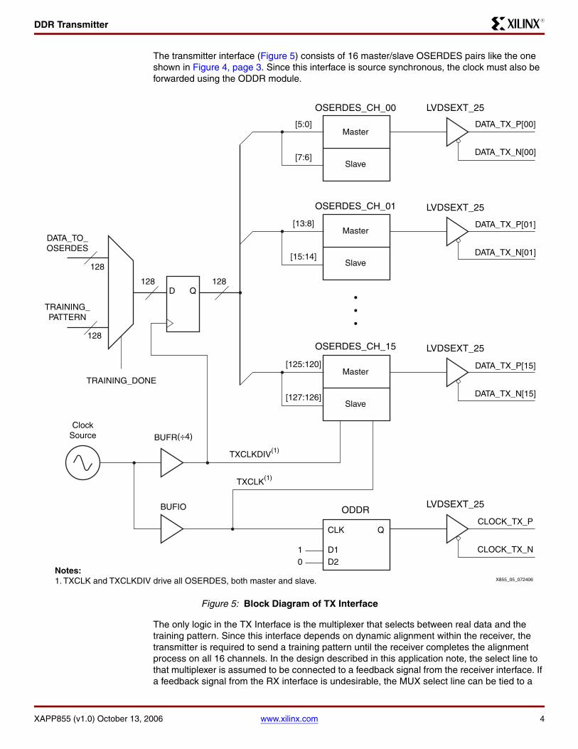
DDR Transmitter
XAPP855 (v10) October 13 2006 wwwxilinxcom 4
R
The transmitter interface (Figure 5) consists of 16 masterslave OSERDES pairs like the one shown in Figure 4 page 3 Since this interface is source synchronous the clock must also be forwarded using the ODDR module
The only logic in the TX Interface is the multiplexer that selects between real data and the training pattern Since this interface depends on dynamic alignment within the receiver the transmitter is required to send a training pattern until the receiver completes the alignment process on all 16 channels In the design described in this application note the select line to that multiplexer is assumed to be connected to a feedback signal from the receiver interface If a feedback signal from the RX interface is undesirable the MUX select line can be tied to a
Figure 5 Block Diagram of TX Interface
MasterDATA_TX_P[00][50]
[76]
[138]
128128
128
128
[1514]
[125120]
[127126]
DATA_TX_N[00]
DATA_TX_P[01]
DATA_TX_N[01]
DATA_TX_P[15]
DATA_TO_OSERDES
TRAINING_PATTERN
ClockSource BUFR(divide4)
TXCLKDIV(1)
TXCLK(1)
BUFIO
DATA_TX_N[15]
QD
Slave
Master
OSERDES_CH_00 LVDSEXT_25
LVDSEXT_25
LVDSEXT_25
CLOCK_TX_P
CLOCK_TX_N
X855_05_072406
LVDSEXT_25
OSERDES_CH_01
TRAINING_DONE
OSERDES_CH_15
ODDR
Slave
Master
CLK Q
D1D2
10
Slave
Notes1 TXCLK and TXCLKDIV drive all OSERDES both master and slave
Interface Clocking
XAPP855 (v10) October 13 2006 wwwxilinxcom 5
R
timer that grants the receiver a fixed amount of time to complete alignment For example the transmitter can transmit the training pattern for 500 ms after which it assumes that the receiver alignment process is complete and sends real data
Table 2 shows the device utilization statistics for the TX interface implemented in a Virtex-5 device Since there is no combinatorial logic in the transmitter no look-up tables (LUTs) are used The 128-bit MUX is implemented using only 128 flip-flops and no combinatorial logic Table 2 also shows one BUFIO and one BUFR being used This design can also be implemented using two BUFGs and a DCM instead The different clocking options for this interface are discussed in ldquoInterface Clockingrdquo
Interface Clocking
In the block diagram of the DDR transmitter shown in Figure 5 page 4 the clock networks are shown driven by BUFIO and BUFR When BUFIO and BUFR are used to generate the serial and parallel clocks the phase relationship between the two clocks is guaranteed by design to meet the input requirements of the OSERDES (and ISERDES) Another valid way of driving the clock networks in Figure 5 is to use global clocks combined with a DCM to divide by four This scheme also provides phase-matched clock outputs guaranteed by design to meet the input requirements of the OSERDES The two valid clocking schemes are shown in Figure 6
Table 2 DDR TX Interface Utilization Statistics
Component Quantity Usage Description
Slice Flip-Flop 128 Registered MUX output of DATA_TO_OSERDES
Slice 32 1284 FFs per slice = 32 slices
LUT 0 ndash
IOB 34 17 LVDS output pairs (16 data 1 clock)
OSERDES 32 Master and slave OSERDES for every LVDS data pair
BUFIO 1 TXCLK
BUFR 1 TXCLKDIV
Figure 6 Global and Regional Clocking Schemes in Virtex-5 FPGAs
BUFR(divideX)
BUFIO
DIVI
OFB
CLKDIV
CLK
OSERDESISERDES
ClockInputGlobal
Scheme
ClockInputChipSync
Scheme
DCMBUFG BUFG
BUFG
CLKDIV
CLK
OSERDESISERDES
X855_06_072406
Interface Clocking
XAPP855 (v10) October 13 2006 wwwxilinxcom 6
R
Which clocking scheme is the best to use The BUFIOBUFR networks maximize performance at the expense of some convenience BUFIO and BUFR are regional clocks that cannot span the entire chip like a global clock This difference means that transferring data between the regional and global domains must be a part of the designers task and can simply mean adding a FIFO between the clock domains
Global clocks have lower performance than BUFIO but are more convenient to use If a clock is placed on a global network it can reach any component in the entire device To show the performance advantage of BUFIO Table 3 shows snapshots of several timing parameters some of which are included in the timing budget calculations for source synchronous interfaces In each case BUFIO has an advantage over BUFG and collectively those advantages are significant These parameters are used in the timing budget calculation section ldquoInterface Timing Budgetrdquo page 18 For the most current specifications always consult the data sheet on wwwxilinxcom
To offer the maximum performance the interface described in this application note uses a BUFIOBUFR clocking scheme in both the transmitter and receiver The interface does not include the FIFO logic necessary to transfer the parallel data tofrom the backend system domain However the BERT design discussed in ldquoIntroductionrdquo page 1 (see Figure 2 page 2) shows how to transfer data tofrom the RX and TX clock domains by using a FIFO18_36 primitive
Table 3 Comparison of Global and IO Clock Performance by Speed Grade
-3 -2 -1 Units
Maximum Frequency
BUFG max frequency 550 500 450 MHz
BUFIO max frequency 710 710 644 MHz
Duty Cycle Distortion
BUFG DYCD 150 150 150 ps
BUFIO DYCD 100 100 100 ps
Sampling Error
BUFG TSAMP 450 500 550 ps
BUFIO TSAMP 350 400 450 ps
Clock Tree Skew
BUFG skew for XC5VLX50T 270 270 270 ps
BUFIO skew for all devices 50 50 50 ps
DDR Receiver
XAPP855 (v10) October 13 2006 wwwxilinxcom 7
R
DDR Receiver The DDR receiver consists of three core modules DDR_8TO1_16CHAN_RX BIT_ALIGN_MACHINE and RESOURCE_SHARING_CONTROL The receiver is more complex than the DDR transmitter because it includes a dynamic alignment algorithm implemented in the FPGA fabric The DDR_8TO1_16CHAN_RX module takes 16 channels of data on the serial side optimizes the timing relationship of each channel with the clock performs 18 deserialization and presents 128 bits of data on the parallel side The port list is shown in Table 4
Table 4 DDR_8TO1_16CHAN_RX Module Port Definitions
Port Name IO Definition
DATA_RX_P [150] Input 16 data channels (P)
DATA_RX_N [150] Input 16 data channels (N)
CLOCK_RX_P Input Forwarded clock (P)
CLOCK_RX_N Input Forwarded clock (N)
INC_PAD Input Pulsing this pin causes the IDELAY tap setting of all data channels to increment by 1
DEC_PAD Input Pulsing this pin causes the IDELAY tap setting of all data channels to decrement by 1
DATA_FROM_ISERDES [1270] Output Parallel side data to backend system
RESET Input Reset synchronous to the RX domain
IDLY_RESET Input Reset synchronous to the RX domain that only resets the IDELAY tap settings of all data channels
IDELAYCTRL_RESET Input Reset synchronous to the TX domain that only resets the IDELAYCTRL module
BITSLIP_PAD Input Pulsing this pin causes one bitslip operation on all data channels
CLK200 Input Reference clock to IDELAYCTRL module
TAP_00 TAP_01 TAP_03 TAP_04 TAP_05 TAP_06 TAP_07 TAP_08 TAP_09 TAP_10 TAP_11 TAP_12 TAP_13 TAP_14 TAP_15
Output[50] Each of these 6-bit signals contains the current IDELAY tap value of the sixteen data channels Possible values 0-63
TAP_CLK [50] Output The 6-bit signal containing the current IDELAY tap value of the clock channel Permanently set to zero because the clock channel is not adjusted
TRAINING_DONE Output Flag indicating alignment is complete
RXCLK Output RX Source Sync Clock
RXCLKDIV Output RX Source Sync Clock divided by 4
IDELAY_READY Output Flag indicating IDELAYCTRL is calibrated
DDR Receiver
XAPP855 (v10) October 13 2006 wwwxilinxcom 8
R
Most of the logic used in the receiver is contained within the ISERDES The ISERDES is part of the ChipSync technology and is found in IO of all Virtex-5 devices The ISERDES can be programmed to do any deserialization up to 110 and do single or double data rate reception For deserializations greater than 61 a second ISERDES is needed (taken from the second IO in the LVDS pair) The first ISERDES is called the master and the second ISERDES is called the slave Figure 7 shows a single channel of the RX
Figure 7 MasterSlave ISERDES Pair for a Single Data Channel with 18 Deserialization
MasterISERDES
Serial DataExternal to
FPGA
X855_07_080306
Parallel Datainto FPGA Fabric
SlaveISERDES
SHIFTOUT2SHIFTOUT1
SHIFTIN2SHIFTIN1
Q1
Q2
Q3
Q4
Q5
Q6
Q1
Q2
Q3
Q4
Q5
Q6
Data8
Data7
Data6
Data5
Data4
Data3
Data2
Data1
DDR Receiver
XAPP855 (v10) October 13 2006 wwwxilinxcom 9
R
The receiver interface (Figure 8) consists of 16 masterslave ISERDES pairs Since this interface is source synchronous the clock source comes from the transmitter The clock is buffered in the receiver by a BUFIO component and divided to the parallel clock rate by a BUFR component
Figure 8 Block Diagram of RX Interface
MasterDATA_RX_P[00]
DATA_RX_N[00]
LVDS_25
Slave
IODELAY
CHAN_SELDATA_ALIGNED
DATA_TO_MACHINE
RXCLK(1)
START_ALIGN
Master
LVDS_25
Slave
ISERDES_CH_01 IODELAY
X855_08_082806
DQ
BUFIO
BUFR (divide4)
8 [72]
[10]
[98]
[1510]
[127122]
[121120]
4
8
8 8
3
3
3
DATA_RX_P[01]
DATA_RX_N[01]
Master
LVDS_25
Slave
IODELAY
DATA_RX_P[15]
DATA_RX_N[15]
ISERDES_CH_15
ISERDES_CH_00
RXCLKDIV
INC
ICE
BITSLIP
RXCLKDIV(1)
INC ICEBITSLIP
To CH 15
To CH 01
To CH 00
RX_IDELAYCTRL
Resource SharingControl
Bit AlignMachine
200 MHzSource
LVDS_25
CLOCK_RX_N
CLOCK_RX_P
Notes1 RXCLK and RXCLKDIV drive all ISERDES both master and slave
IODELAY
Fixed to Tap 0
Decoder
DDR Receiver
XAPP855 (v10) October 13 2006 wwwxilinxcom 10
R
Each ISERDES in Figure 8 page 9 contributes 8 bits to the 128-bit parallel data bus Since there is only one instance of BIT_ALIGN_MACHINE in the receiver each data channel must be aligned separately by sharing that resource The 8-bit data buses from each ISERDES are fed into a MUX which selects which of the 16 channels has access to the BIT_ALIGN_MACHINE resource RESOURCE_SHARING_CONTROL controls the MUX to ensure that every channel completes its alignment before the MUX switches to the next channel The START_ALIGN signal tells the BIT_ALIGN_MACHINE that alignment can begin on the current channel because the MUX output is stable The DATA_ALIGNED signal tells the RESOURCE_SHARING_CONTROL module that alignment on the current channel is complete
The order of the parallel data outputs of the ISERDES is the opposite of the parallel data inputs of the OSERDES The least significant OSERDES data inputs are fed into the master while the least-significant ISERDES data outputs come from the slave (Figure 4 page 3 versus Figure 7)
The IDELAYCTRL module in Figure 8 is shown as having no connection to the rest of the receiver Actually IDELAYCTRL is required to calibrate the IODELAY blocks in the path of each data channel A single IDELAYCTRL block is sufficient to calibrate all 16 data channels since all channels are in the same bank
The BIT_ALIGN_MACHINE generates three control signals that adjust the timing of the appropriate ISERDES INC and ICE cause the IODELAY to increment or decrement the delay in the datapath by a fixed amount of ~75 ps (if a 200 MHz reference clock is used) BITSLIP causes each ISERDES to rotate the order of the parallel output data bits facilitating the process of word alignment These three control signals are directed to the appropriate ISERDES by the decoder shown in Figure 8 Although not shown in the figure the decoder is also controlled by the RESOURCE_SHARING_CONTROL module
Table 5 shows the device utilization statistics for the RX interface implemented in a Virtex-5 device These figures exclude the counters used to track the IODELAY settings on all data channels in most instances those counters can be removed after the interface is integrated and verified in a specific environment The majority of the LUTs utilized are consumed by the BIT_ALIGN_MACHINE which is the core of the receiver alignment algorithm As in the TX interface the RX interface consumes one BUFIO and one BUFR for clocking The clocking could also be accomplished using BUFGs and a DCM as described in ldquoInterface Clockingrdquo page 5 but the performanceconvenience trade off would need to be considered
Table 5 DDR RX Interface Utilization Statistics
Component Quantity Usage Description
Slice Flip-Flop 131 Multiple uses
Slice 105 Multiple uses
LUT 263 Multiple uses
IOB 34 17 LVDS input pairs (16 data 1 clock)
ISERDES 32 Master and slave ISERDES for every LVDS data pair
BUFIO 1 RXCLK
BUFR 1 RXCLKDIV
Receiver Interface Dynamic Timing
XAPP855 (v10) October 13 2006 wwwxilinxcom 11
R
Receiver Interface Dynamic Timing
The timing of the receiver interface is broken into two parts
bull The suboptimal timing inherent in the data and clock paths
bull The optimal timing created by the receiver when adjusting dynamic delays on each of the 16 data channels
Inherent Timing
An inventory of all propagation delays in the clock and datapaths must be taken to derive the inherent setuphold times The clock and datapaths for a single channel of this interface are shown in Figure 9 The ISE Timing Analyzer breaks down the paths into the timing parameters shown All components in the path have both a minimum and maximum value to account for process variations
Figure 10 page 12 shows the timing analyzer settings used to generate the information in this report Each of the timing parameters is described in Table 6 page 12 and Table 7 The minimum and maximum values of the individual timing parameters for the clock and datapaths are shown in Table 8 and Table 9 page 13
Note All raw timing numbers referenced in this document are subject to minor changes in subsequent revisions of the ISE tools
Figure 9 Timing Components of RX Data and Clock Paths
ISERDESFFsIODELAY
VariableInit to 0
DI O
CLK
IODELAYIBUFDS
IBUFDS
+
ndash
+
ndash Fixed toTap 0
I O
X855_09_082806
DataPath
ClockPath
TIOPI TIODDO_IDATAINTNET1 TNET2
TIOPI TIODDO_IDATAIN TISDCK_DDLY
TBUFIOCKO_O
BUFIO
Receiver Interface Dynamic Timing
XAPP855 (v10) October 13 2006 wwwxilinxcom 12
R
Figure 10 ISE Timing Analyzer Properties Used in this Document
Table 6 Datapath Timing Definitions
Timing Parameter Description
TIOPI Delay from the IOB pad through the LVDS input buffer to the I pin of the IOB pad
TIODDO_IDATAIN Delay from the I pin of IOB pad to the D input of the ISERDES
TISDCK_DDLY Delay from the D input of the ISERDES to the sampling registers in the ISERDES (setup and hold times of ISERDES)
Table 7 Clock Path Timing Definitions
Timing Parameter Description
TIOPI Delay from the IOB pad through the LVDS input buffer to the I pin of the IOB pad
TIODDO_IDATAIN Delay from I pin of IOB pad to the O output of the IODELAY block
TNET1 Delay from the O output of the IODELAY block to the I pin of BUFIO
TBUFIOCKO_O Clock to out delay of BUFIO
TNET2 Clock distribution delay from BUFIO output to the clock input of data ISERDES
Table 8 Datapath Delay Inventory for a -1 Speed Grade XC5VLX50T Device
Timing Parameter Maximum Datapath Delay Minimum Datapath Delay
TIOPI 1083 ns 0763 ns
TIODDO_IDATAIN 0671 ns 0671 ns
TISDCK_DDLY 0064 ns ndash0038 ns
TOTAL 1818 ns 1396 ns
XAPP855_10_071306
Receiver Interface Dynamic Timing
XAPP855 (v10) October 13 2006 wwwxilinxcom 13
R
According to the inherent timing prediction the data is going to arrive before the clock by an amount determined by Equation 1 and Equation 2 Equation 1 calculates that data arrives before the clock by at least 1076 ns in a -1 device Equation 2 calculates that data arrives before the clock by at most 2213 ns Equation 3 shows a timing window that covers all -1 devices under all conditions This timing window describes the inherent timing of the data and clock paths Assuming skew-matched PCB traces for all sixteen channels then it can be assumed that all 16 channels in the receiver have roughly the same timing window
Equation 1
Equation 2
Equation 3
Figure 11 shows the timing windows for all speed grades of an XC5VLX50T device as well as a hardware measurement of the inherent timing relationship (to validate the calculations) The hardware measurement shows the DDR interface data arriving 1425 ns before the clock which by inspection places the device in all three speed grade ranges (the device used for the hardware measurement is a -2 device)
Table 9 Clock Path Delay Inventory for a -1 Speed Grade XC5VLX50T Device
Timing Parameter Maximum Clock Path Delay Minimum Clock Path Delay
TIOPI 1150 ns 0820 ns
TIODDO_IDATAIN 0671 ns 0671 ns
TNET1 0254 ns 0190 ns
TBUFIOCKO_O 1130 ns 0894 ns
TNET2 0404 ns 0319 ns
TOTAL 3609 ns 2894 ns
Setup Time Max Data Delay Min Clock Delay 1818 2894ndash 1076 nsndash==ndash=
Hold Time Max Clock Delay Min Data Delay 3609 1396ndash 2213 ns==ndash=
Timing Window 2213 1076ndash 1137 ns==
Figure 11 Timing Windows Show Uncertainty in ClockData Relationship as Calculated by Timing Analyzer
400 Mbs Data (T = 25 ns)
1425 ns Hardware MeasurementData Arrives
x855_11_091806
-11076ns 2213 ns
-21043 ns 2039 ns
-30989 ns 1878 ns
Receiver Interface Dynamic Timing
XAPP855 (v10) October 13 2006 wwwxilinxcom 14
R
Dynamic Timing and BIT_ALIGN_MACHINE
In ldquoInherent Timingrdquo page 11 the inherent timing of the interface was calculated for all speed grades and validated with a hardware measurement In that case the inherent timing was sufficient because the data rate is only 400 Mbs (Figure 11 page 13) What happens when the data rate is increased such that the hold edge of the data window begins to shrink (Figure 12)
At 600 Mbs the inherent timing relationship is no longer adequate to meet timing because there are cases when the sampling clock edge is in the middle of the data transition As the data rates increase to 800 and 1000 Mbs the clock actually captures the data arriving one bit time later For designs that are sensitive to word alignment this is unacceptable
The solution to the suboptimal inherent timing is dynamic timing The BIT_ALIGN_MACHINE module in the receiver performs two functions of dynamic timing
bull Bit Alignment Position the sampling edge of the clock at the center of the data eye by adding delay to the datapaths
bull Word Alignment Ensure that the parallel data bits are in the correct order at the output of the ISERDES by using the bitslip function in the ISERDES
The steps of the bit-alignment procedure are shown in Figure 13 page 15 Each step of the algorithm can either add or subtract delay from the datapath All 16 channels are taken through this procedure independently This procedure measures one full data eye (in terms of 75 ps delay taps) and then returns to the center of the data eye Steps 1 and 2 are dedicated to moving through the partial eye of the initial timing while steps 3 and 4 are dedicated to measuring a full eye Step 5 is dedicated to positioning the clock edge at the center of the data eye
Figure 12 Inherent Timing Windows Shown in Relation to Multiple Data Rates
400 Mbs Data (T = 25 ns)
600 Mbs Data (T = 167 ns)
800 Mbs Data (T = 127 ns)
1000 Mbs Data (T = 10 ns)
-11076ns 2213 ns
-21043 ns 2039 ns
-30989 ns
1425 ns
1878 ns
Hardware MeasurementData Arrives
x855_12_091806
Receiver Interface Dynamic Timing
XAPP855 (v10) October 13 2006 wwwxilinxcom 15
R
Jitter is represented in Figure 13 as multiple transition lines Accounting for jitter is a crucial part of the algorithm In step 2 the first data transition is found If there is no jitter then the eye measurement can begin instantly after finding the transition However when jitter is considered the algorithm must find the first transition move through the transition and then begin looking for the second transition If the algorithm does not move through the first transition intelligently it runs the risk of falsely detecting the second transition
Once bit alignment is complete the order of the data bits can be adjusted to achieve word alignment The bit-alignment procedure ensures that data is being sampled correctly but the order of the data can be a few bits off from where the receiver expects it to be To correct this the bitslip feature of the ISERDES is used to slip bit times until the proper alignment is found For this feature to be useful a training pattern must be generated by the transmitter (as discussed in ldquoDDR Transmitterrdquo page 3) that the receiver can use to determine the proper word alignment In this reference design the training pattern is 00101100 (0x2C) This pattern is mostly arbitrary as many other patterns work just as well This pattern was chosen because a training pattern should behave electrically as much like real data as possible such that the center of the training eye is the center of the data eye Since real data contains strings of consecutive ones and zeros it is best for the training pattern to do the same For that reason a 0x2C pattern is better than an 0xAA pattern because it contains run lengths of 1 2 3 and 4 bit times
Table 10 page 16 shows the word-alignment process in the case where bit alignment completes with the data outputs set to 0x58 Since 0x58 is not the training pattern the receiver is looking for bitslip is asserted until 0x2C is found This reference design uses a 18 deserialization so there are only eight possible configurations of the parallel data outputs If bitslip is asserted infinitely the same eight configurations will repeat Bitslip in DDR mode is somewhat irregular because it does not simply rotate by one bit on every bitslip cycle This effect is inconsequential to the word-alignment procedure (see the Virtex-5 User Guide for more details)
Figure 13 Dynamic Bit-Alignment Procedure in BIT_ALIGN_MACHINE
Data 0
Data Arrives Before Clock
Data 1
x855_13_091806
Data 0 Data 1
Data 0 Data 1
Data 0 Data 1
Data 0 Data 1
Sampling Clock (Fixed Delay)
Return to Center of Eye
End Measuring Eye
Begin Measuring Eye
Find 1st Transition
Initial Timing1
2
3
4
5
Receiver Interface Dynamic Timing
XAPP855 (v10) October 13 2006 wwwxilinxcom 16
R
The FSM in the BIT_ALIGN_MACHINE module used to implement both bit and word alignment is shown in Figure 14 page 17 The FSM is divided into five sections loosely described as finding the first transition getting through the first transition finding the second transition returning to the center of the eye and word alignment
To get through the first transition effectively for all possible types of jitter two methods are used The first method pertains to random jitter If there is a lot of random jitter at the sampling point then the samples generated are not stable The algorithm detects this instability by comparing current samples to older samples and therefore knows where the transition begins and ends But what if the jitter is extremely deterministic The transition then has discreet crossing points such that within the transition there is very stable but incorrect data In this case the algorithm does not sense any instability and falsely concludes that the sampling point is not in the transition To address this case apart from evaluating stability the algorithm also evaluates the correctness of the data content by using the bitslip feature in the middle of the transition For example if the algorithm determines that the sampled data is stable it then asserts bitslip to look for the correct data If 0x2c is found within eight assertions of bitslip then the sampling point is not in the transition But if 0x2c is not found then the algorithm increments the data delay and repeats the transition test again
Table 10 Word Alignment in the DDR Receiver
Bitslip Cycle Data Value (Hex) Data Value (Bin) Description of Bitslip operation
1 58 0101 1000 ndash
2 0B 0000 1011 Rotate 3 bits to right
3 16 0001 0110 Rotate 1 bit to left
4 C2 1100 0010 Rotate 3 bits to right
5 85 1000 0101 Rotate 1 bit to left
6 B0 1011 0000 Rotate 3 bits to right
7 61 0110 0001 Rotate 1 bit to left
8 2C 0010 1100 Rotate 3 bits to right
Receiver Interface Dynamic Timing
XAPP855 (v10) October 13 2006 wwwxilinxcom 17
R
Figure 14 FSM in the BIT_ALIGN_MACHINE Module
TRANSITION_CHECK (01000)
First TransitionNot Detected
First TransitionNot Detected
First TransitionDetected
First TransitionDetected
Past the FirstTransition
Second TransitionNot Detected
Second TransitionDetected
Decrement DelayAgain
Bit AlignmentComplete
Still Samplingin Transition
INC_ONCE (01111)
SEARCH_PAT (01101)
IDLE (01100)
IDLE (10000)
RECHECK_TRANS (00010)
ONE_BITSLIP (00110)
INC_ONCE (01011)
WAIT_8_CYCLES (00100)
COUNT_1 (01110)
INC_ONCE (01001)
WAIT_8_CYCLES (00011)
IDLE (10010)
TRAINING_DONE (00111)
FIRST_SAMPLE (00001)
RESET (00000)
DEC_TO_HALF (01010)
WORD_ALIGN (00101)
X855_14_082806
Routine to Avoid False Detection of Second Transition
=CHECK_PATTERN
Receiver Interface Dynamic Timing
XAPP855 (v10) October 13 2006 wwwxilinxcom 18
R
Interface Timing Budget
In addition to sampling the data as closely as possible to the center of the data eye the actual size of the data eye is important By accurately predicting the size of the data eye in the receiver the overall performance ceiling of the interface can be inferred The ideal data eye width is the period of the data rate (for example TBit_Period = 100 ns for 1000 Mbs) Both the transmitter and receiver circuits have sources of error that subtract from the ideal data eye The equation for the eye width at the output of the transmitter is shown in Equation 4 TJITTER is the peak-to-peak jitter of the clock source driving the transmitter data bus and forwarded clock TDCD is the maximum duty cycle distortion of the clock tree driving the data bus and forwarded clock Skew is not considered in the transmitter or receiver because the receiver calibrates out skew between channels by performing alignment on each channel individually
Equation 4
Equation 5 calculates the width of the data eye at the receiver flip-flops Ideally the eye width at the receiver is the same as the eye width at the output of the transmitter but there are sources of error in the transmission medium and receiver circuitry Duty cycle distortion must be considered again on the receiver clock tree TSAMP_BUFIO is the receiver sampling error due to drift caused by voltage and temperature variations TIDELAYPAT_JIT is the amount of pattern dependent jitter that is accumulated in each tap of the IDELAY chain For a clock pattern TIDELAYPAT_JIT is 0 pstap peak to peak For a data pattern with long and short run lengths of zeroes and ones (simulated by PRBS23) TIDELAYPAT_JIT is a finite value that must be considered in the timing budget
Equation 5
TBOARD_JITTER includes jitter induced by receiver input capacitance and the parasitics of the physical data path on the PCB TBOARD_JITTER must be determined by simulation as it varies as a function of frequency and for receivers of different types and vendors On the ML550 with a -2 speed-grade Virtex-5 device the TBOARD_JITTER is measured at roughly 200 ps at 900 Mbs (assuming data content equivalent to PRBS23) TQUANTIZATION_ERR or quantization error is caused by the granularity of the IDELAY tap chain Working with 75 ps increments it is not possible to utilize the entire data eye since inevitably some valid eye width is lost between two taps The value for this loss is 75 ps As long as the receiver eye width calculated using Equation 5 is greater than or equal to 0 the interface operates correctly over process voltage and temperature
For example Equation 6 and Equation 7 show the timing budget calculation for the DDR interface running at 900 Mbs in a -2 speed grade device on an ML550 evaluation board Refer to the data sheet for the most current values The TX interface is looped back to the RX interface on the same Virtex-5 FPGA as shown in Equation 2
Equation 6
Equation 7
Changes in voltage and temperature cause the data channels of the interface to drift relative to the clock If the DDR interface were to transfer user data for a long period of time over all specified conditions of temperature and voltage Equation 7 states that there would be at least 107 ps (one or two IDELAY taps) of data window remaining valid during all fluctuations of temperature and voltage Compare this calculation to the measurements in Table 12 page 21 Case 900 Mbs There are four taps that are error free under all conditions In ldquoAppendixrdquo there are three -2 devices tested at 900 Mbs and each has 4 4 and 3 taps respectively that are error free under all conditions
DATA_EYE_WIDTH_TX TBIT_PERIOD TJITTERndash TDCD_BUFIOndash=
DATA_EYE_WIDTH_RX DATA_EYE_WIDTH_TX
TBOARD_JITTER
ndash
TSAMP_BUFIOndash TDCD_BUFIOndash
TIDELAYPAT_JIT IDELAY taps in datapathtimes[ ]ndash
TQUANTIZATION_ERRndash
=
DATA_EYE_WIDTH_TX 1111 ps 25 psndash 100 psndash 986 ps= =
DATA_EYE_WIDTH_RX986 ps 200 psndash 400 psndash 100 psndash 8 ps 13 tapstimes[ ] 75 ps 107 ps=ndashndash
=
Interface Characterization
XAPP855 (v10) October 13 2006 wwwxilinxcom 19
R
At a given temperature and voltage setting the data valid window is much larger because there is no drift when temperature and voltage are constant The size of the data valid window under constant conditions is 107 ps + TSAMP_BUFIO which in this case is at least 507 ps (six or seven IDELAY taps) Compare this calculation to the measurements of any single condition in Table 12 Case 900 Mbs In the worst case (ndash5 supply) there are 7 taps that are error free
Equation 8 and Equation 9 show the same timing budget calculation for the DDR interface running at 10 Gbs in a -2 speed grade device on an ML550 Evaluation Board
Equation 8
Equation 9
Equation 9 predicts that no data window remains valid during all specified fluctuations of temperature and voltage (compare to Table 12 Case 1000 Mbs) In ldquoAppendixrdquo there are three -2 devices tested at 1000 Mbs and each has 1 3 and 1 taps respectively that are error free under all conditions This data rate and device combination are very marginal cases
To operate at 10 Gbs the DDR interface requires additional circuitry to track out voltage-temperature variations in real-time (see XAPP860 16-channel DDR LVDS Interface with Real-time Window Monitoring for a DDR Interface with real-time window monitoring) If the voltage-temperature variations are removed from the picture the predicted data valid window is ndash120 ps + TSAMP_BUFIO which in this case is at least 280 ps (3 or 4 taps) Compare this calculation to the measurements of any single condition in Table 18 page 34 There are at least four error-free taps in all conditions
Interface Characterization
By following the procedure illustrated in Figure 13 page 15 the bit-alignment algorithm should never insert more than approximately 15 bit times of delay on the data channels The fewest number of delay taps should be used in the datapath because they produce a finite amount of degradation (TIDELAYPAT_JIT) The worst-case initial timing for the algorithm occurs when the clock samples just before the data transitions as in the 600 Mbs case in Figure 12 page 14 The algorithm must move all the way through the first eye to find the first transition (1 bit time) and then move halfway into the next eye to center the sampling point (05 bit time) This process produces a worst-case total delay insertion of 15 bit times
The actual performance of the bit-alignment algorithm is characterized as a function of data rate in Figure 15 page 20 For all data rates the expectation is that the tap settings of all 16 channels in the DDR receiver do not exceed approximately 15 bit times of delay Both the maximum and minimum tap setting of all 16 channels is recorded for each data rate This graph only shows the data for a single device Comparing the 15 bit time mask to the actual settings it is clear that the algorithm remains within the 15 bit time limit At 13 Gbs the tap setting actually exceeds the mask by one tap (a negligible violation)
DATA_EYE_WIDTH_TX 1000 ps 25 psndash 100 psndash 875 ps= =
DATA_EYE_WIDTH_RX 875 ps 300 psndash400 ps 100 psndash
ndash8 ps 15 tapstimes[ ] 75 ps 120 psndash=ndashndash
=
Interface Characterization
XAPP855 (v10) October 13 2006 wwwxilinxcom 20
R
The maximum and minimum tap settings in Figure 15 generally stay within 3 to 4 taps of each other except in the case of 640 Mbs and 1300 Mbs data rates These data rates are seams in the inherent timing At data rates below 640 Mbs the tap settings are in the range of 30 taps and at data rates above 640 Mbs the tap settings are in the range of 12 taps Referring back to Figure 12 page 14 it is clear why this seam occurs As the data rate increases past 600 Mbs the initial sampling point of the inherent timing moves into a different data eye creating a different starting point for the algorithm At 640 Mbs some of the 16 channels start in one eye while other channels start in the other eye Fortunately this is not an issue because the single bit time of difference between the channels is resolved using bitslip
Referring back to Figure 8 page 9 the clock channel goes through an IDELAY block with a default value of 0 Once the data rate is chosen for a given design this initial IDELAY value can be changed to a non-zero value to achieve more favorable inherent timing For example a design running at 620 Mbs can use 30 IDELAY taps on the delay channels each contributing a certain amount of jitter to the timing budget calculation By setting the initial clock delay to 5 taps the inherent timing moves across the seam shown in the 600 Mbs range of Figure 15 causing the data channels to only use about 12 IDELAY taps Only spectrally rich data patterns accumulate jitter in the IDELAY tap chain so the clock IDELAY can be set to any value without diminishing the timing budget This optimization is entirely optional and can be done once the design is running in hardware
The DDR receiver is designed to remove skew between channels by aligning each channel individually The ML550 board on which this reference design is characterized is designed to have minimal skew between channels However there is clearly a finite amount of skew between channels due to clock skew in the TX and RX BUFIO networks package skew and trace length tolerance on the ML550 board Table 11 page 21 shows how the bit-alignment algorithm sets the delay for each channel differently to compensate for skew between channels The table captures the range of settings among the 16 channels at specific data rates for a -2 device If there were additional skew among the 16 channels then the tap setting range would be larger to compensate for it The algorithm is designed such that skew between channels should not diminish the performance of the interface The range of tap settings differs for different devices and speed grades but the magnitude should be approximately the same
Figure 15 Bit-Alignment Algorithm Performance
60
50
40
30
20
10
0200 400 600 800 1000 1200 1400 1600
Data Rate (Mbs)
Del
ay T
ap U
tiliz
atio
n HW Measurement (Min)HW Measurement (Max)15 Bit Time Mask
X855_15_072406
Interface Characterization
XAPP855 (v10) October 13 2006 wwwxilinxcom 21
R
Since the receiver alignment logic only runs once immediately after reset the resulting dynamic timing must be adequate to ensure error-free operation over the specified voltage and temperature variations that can occur over time The data-valid window at the receiver input must be wide enough to withstand these variations (receiver drift) Table 12 page 21 shows the data-valid window at the ISERDES registers in the DDR receiver The eyes shown are collective eyes of all 16 channels The BERT testbench configuration loops back the DDR transmitter to the DDR receiver Using pattern generators and error detectors programmed to send and receive a pseudorandom bit sequence (PRBS23) the width of the data-valid window is evaluated using pseudorandom data that closely resembles real user data
Table 11 Tap Setting Range For Various Data Rates Measured on a -2 Device
Data Rate (Mbs) Tap Setting Range Compensated Skew
500 31ndash34 4 taps
600 28ndash30 3 taps
700 10ndash12 3 taps
800 11ndash13 3 taps
900 11ndash13 3 taps
1000 13ndash15 3 taps
1100 13ndash15 3 taps
1200 14ndash15 2 taps
Table 12 Measurement of Receiver Drift under Extreme Conditions for Multiple Data Rates
ConditionIODELAY Taps (1)
ndash8 ndash7 ndash6 ndash5 ndash4 ndash3 ndash2 ndash1 0 +1 +2 +3 +4 +5 +6 +7 +8
Case 800 Mbs
25degC Nom Supplies F F F P P P P P C P P P P P F F F
0degC Nom Supplies F F F P P P P P P P P P P P F F F
85degC Nom Supplies F F F P P P P P P P P P P P F F F
25degC +5 Supplies F P P P P P P P P P P P F F F F F
0degC +5 Supplies F P P P P P P P P P P P F F F F F
85degC +5 Supplies F P P P P P P P P P P P F F F F F
25degC ndash5 Supplies F F F F F F P P P P P P P P P F F
0degC ndash5 Supplies F F F F F F P P P P P P P P P P F
85degC ndash5 Supplies F F F F F P P P P P P P P P P F F
CONCLUSION Error free under all conditions when calibrated under nominal conditions to position C
Interface Characterization
XAPP855 (v10) October 13 2006 wwwxilinxcom 22
R
Case 900 Mbs
25degC Nom Supplies F F F F P P P P C P P P P F F F F
0degC Nom Supplies F F F F P P P P P P P P P F F F F
85degC Nom Supplies F F F F P P P P P P P P F F F F F
25degC +5 Supplies F F P P P P P P P P P F F F F F F
0degC +5 Supplies F F P P P P P P P P P F F F F F F
85degC +5 Supplies F F P P P P P P P P P F F F F F F
25degC ndash5 Supplies F F F F F F F P P P P P P P P F F
0degC ndash5 Supplies F F F F F F F P P P P P P P P F F
85degC ndash5 Supplies F F F F F F F P P P P P P P F F F
CONCLUSION Error free under all conditions when calibrated under nominal conditions to position C
Case 1000 Mbs
25degC Nom Supplies F F F F F P P P C P P P F F F F F
0degC Nom Supplies F F F F F P P P P P P P F F F F F
85degC Nom Supplies F F F F F P P P P P P P F F F F F
25degC +5 Supplies F F F P P P P P P P F F F F F F F
0degC +5 Supplies F F F P P P P P P P F F F F F F F
85degC +5 Supplies F F F P P P P P P P P F F F F F F
25degC ndash5 Supplies F F F F F F F F P P P P P P F F F
0degC ndash5 Supplies F F F F F F F F P P P P P P F F F
85degC ndash5 Supplies F F F F F F F F P P P P P P F F F
CONCLUSION Error free under all conditions when calibrated under nominal conditions to position C
Case 1100 Mbs
25degC Nom Supplies F F F F F P P P C P F F F F F F F
0degC Nom Supplies F F F F F P P P P P F F F F F F F
85degC Nom Supplies F F F F F P P P P P F F F F F F F
25degC +5 Supplies F F F P P P P P P F F F F F F F F
0degC +5 Supplies F F F P P P P P P F F F F F F F F
85degC +5 Supplies F F F P P P P P P F F F F F F F F
25degC ndash5 Supplies F F F F F F F F P P P P F F F F F
0degC ndash5 Supplies F F F F F F F F P P P P F F F F F
85degC ndash5 Supplies F F F F F F F F P P P P F F F F F
CONCLUSION Error free under all conditions when calibrated under nominal conditions to position C
Table 12 Measurement of Receiver Drift under Extreme Conditions for Multiple Data Rates (Continued)
ConditionIODELAY Taps (1)
ndash8 ndash7 ndash6 ndash5 ndash4 ndash3 ndash2 ndash1 0 +1 +2 +3 +4 +5 +6 +7 +8
Interface Characterization
XAPP855 (v10) October 13 2006 wwwxilinxcom 23
R
In all test cases shown in Table 12 page 21 the bit-align machine accurately places the sampling point in the center of the data eye (indicated by the C in each test case) In the 1100 Mbs case the bit-align machine places the sampling point slightly off center This slight inaccuracy occurs when the center of a real data pattern diverges from the center of the training pattern The electrical behavior of different data patterns is discussed below
After the dynamic timing is established for a given test case under nominal conditions the device is subjected to extremes of temperature and voltage to stress the receiver timing At data rates of 1100 Mbs and below the dynamic timing established after reset under nominal conditions is sufficient to meet timing over all specified extreme conditions (the column with the C passes traffic error free under all conditions) At a data rate of 1200 Mbs the design operates correctly under nominal conditions but the data-valid window is not large enough to withstand the voltage variations For this particular transmission medium the 1200 Mbs case requires a real-time adjustment circuit that could track the center of the eye
The full datapath of the testbench consists of
TX rarr 5 FR-4 rarr SAMTEC QSE Conn rarr 12 Ribbon Cable rarr SAMTEC QSE Conn rarr 5 FR-4 rarr RX
For shorter transmission media higher performance can be achieved in accordance with the section ldquoInterface Timing Budgetrdquo page 18 Interface performance is not solely a question of the LVDS driver performance specification but rather a question of adequate timing margin to withstand production and environmental variations From Table 12 the total amount of variation experienced over temperature and voltage is roughly 375 ps (5 taps at 75 ps per tap) This number should be comparable to the specification for receiver sampling error (TSAMP_BUFIO) shown in the Virtex-5 Data Sheet
Case 1200 Mbs
25degC Nom Supplies F F F F F F P P C P F F F F F F F
0degC Nom Supplies F F F F F F P P P P F F F F F F F
85degC Nom Supplies F F F F F F P P P F F F F F F F F
25degC +5 Supplies F F F F P P P P F F F F F F F F F
0degC +5 Supplies F F F P P P P P F F F F F F F F F
85degC +5 Supplies F F F F P P P P F F F F F F F F F
25degC ndash5 Supplies F F F F F F F F F P P P F F F F F
0degC ndash5 Supplies F F F F F F F F F P P P F F F F F
85degC ndash5 Supplies F F F F F F F F F P P F F F F F F
CONCLUSION Errors caused by plusmn5 variations in supply voltages
Notes 1 Where 0 is the reference tap determined by the bit-align machine under nominal conditions at 25degC2 P = Error-free transmission F = Error in transmission C = IODELAY tap position selected by bit-align machine under nominal conditions at 25degC3 Device under test is -2 speed grade
Table 12 Measurement of Receiver Drift under Extreme Conditions for Multiple Data Rates (Continued)
ConditionIODELAY Taps (1)
ndash8 ndash7 ndash6 ndash5 ndash4 ndash3 ndash2 ndash1 0 +1 +2 +3 +4 +5 +6 +7 +8
Interface Characterization
XAPP855 (v10) October 13 2006 wwwxilinxcom 24
R
Pattern Dependence of Receiver Performance
Different types of data patterns have different electrical signatures (rise and fall times jitter eye symmetry etc) A pattern with very narrow spectral content (such as a clock pattern) moves very favorably through the link because the receiver frequency response has little effect on the signal integrity However a pattern with wide spectral content (such as real data and pseudorandom patterns) stresses the links frequency response If the frequency response is not flat across the entire spectrum of the data content then the signal integrity is degraded as a result The amount of degradation measured is shown in Table 13 page 25 The DDR transmitter is looped back to the DDR receiver and different patterns are programmed to traverse the link Performance is assessed by evaluating the integrity of those patterns in the receiver
PRBS7 is a pseudorandom data pattern with a maximum run length of seven consecutive zeroes or ones PRBS15 is defined as having a maximum run length of fifteen consecutive zeroes or ones These limitations on run lengths limit the spectral content of the pattern A PRBS15 pattern has greater spectral content than a PRBS7 pattern and therefore is a more strenuous test for the link PRBS29 is the most strenuous test in Table 13 A clock pattern is effectively a PRBS1
As predicted Table 13 shows that there is more degradation for data patterns with more spectral content At 1000 Mbs and below the data eye closure is symmetrical Symmetrical eye closure is desired because it does not change the center of the eye as determined by the bit-alignment algorithm Above 1000 Mbs the eye closure becomes more asymmetrical causing the center of the data eye to diverge from the calibrated center (by only 1 tap)
In every data rate shown in Table 13 all significant pattern-dependent degradation is caused between PRBS1 (clock pat) and PRBS15 Between PRBS15 and PRBS29 there is no additional degradation recorded in any of the measurements
Interface Characterization
XAPP855 (v10) October 13 2006 wwwxilinxcom 25
R
Table 13 Link Performance for Various Types of Data Measured on a -2 Device
PatternIODELAY Taps (1)
ndash8 ndash7 ndash6 ndash5 ndash4 ndash3 ndash2 ndash1 0 +1 +2 +3 +4 +5 +6 +7 +8 +9
Case 600 Mbs
Clock Pat (0101) P P P P P P P P C P P P P P P P P P
Training Pat (0x2C) P P P P P P P P C P P P P P P P P F
PRBS7 P P P P P P P P C P P P P P P P P F
PRBS15 F P P P P P P P C P P P P P P P F F
PRBS23 F P P P P P P P C P P P P P P P F F
PRBS29 F P P P P P P P C P P P P P P P F F
Case 800 Mbs
Clock Pat (0101) F F P P P P P P C P P P P P P F F F
Training Pat (0x2C) F F P P P P P P C P P P P P P F F F
PRBS7 F F P P P P P P C P P P P P F F F F
PRBS15 F F F P P P P P C P P P P P F F F F
PRBS23 F F F P P P P P C P P P P P F F F F
PRBS29 F F F P P P P P C P P P P P F F F F
Case 1000 Mbs
Clock Pat (0101) F F F P P P P P C P P P P P F F F F
Training Pat (0x2C) F F F P P P P P C P P P P F F F F F
PRBS7 F F F F P P P P C P P P F F F F F F
PRBS15 F F F F F P P P C P P P F F F F F F
PRBS23 F F F F F P P P C P P P F F F F F F
PRBS29 F F F F F P P P C P P P F F F F F F
Case 1200 Mbs
Clock Pat (0101) F F F F P P P P C P P P P F F F F F
Training Pat (0x2C) F F F F P P P P C P P P F F F F F F
PRBS7 F F F F F P P P C P F F F F F F F F
PRBS15 F F F F F F P P C F F F F F F F F F
PRBS23 F F F F F F P P C F F F F F F F F F
PRBS29 F F F F F F P P C F F F F F F F F F
Case 1400 Mbs
Clock Pat (0101) F F F F F F P P C P P P F F F F F F
Training Pat (0x2C) F F F F F P P P C P P F F F F F F F
PRBS7 F F F F F F F P C P F F F F F F F F
PRBS15 F F F F F F F P C F F F F F F F F F
PRBS23 F F F F F F F P C F F F F F F F F F
PRBS29 F F F F F F F P C F F F F F F F F F
Notes 1 Where 0 is the reference tap determined by the bit-align machine under nominal conditions at 25degC2 P = Error-free transmission F = Error in transmission C = IODELAY tap position selected by bit-align machine under nominal conditions at 25degC
Resetting the Interface
XAPP855 (v10) October 13 2006 wwwxilinxcom 26
R
Resetting the Interface
Several dependencies determine the order in which circuits should be reset in the interface The receiver cannot begin the alignment algorithm if the transmitter is not sending the training pattern The transmitter must be reset before the receiver and time must be allowed for the training pattern to propagate across the link before the receiver comes out of reset The receiver also cannot begin the alignment algorithm until IDELAYCTRL has recovered from reset which could takes hundreds of cycles The recommended reset timing for the interface is shown in Figure 16 This reset timing is implemented in the BERT testbench for this interface
The TX reset (RST_TX) is used to reset all TX circuitry and also IDELAYCTRL The IDELAYCTRL reset is asynchronous so driving it with RST_TX is acceptable The minimum pulse width of IDELAYCTRL reset is 50 ns (TIDELAYCTRL_RPW) For that reason resets are held High for 16 clock cycles The RX reset (RST_RX) is used to reset all RX circuitry and is asserted when the IDELAYCTRL READY flag goes High indicating that the IODELAY blocks are calibrated
The timing of the READY flag in Figure 16 is a potential hazard Most likely it is High during a TX reset because it takes many cycles for IDELAYCTRL to deassert the READY flag It is easy to make the mistake of resetting the receiver too early To avoid this hazard the RX reset should be asserted only after seeing a deassertion and reassertion of the READY flag
Conclusion Based on the design and characterization described in this document the 16-Channel DDR reference design operates to the performance targets in Table 14 under all conditions of process voltage and temperature However to meet these targets over voltage and temperature the timing budget must be guaranteed according to the analysis in ldquoInterface Timing Budgetrdquo See ldquoAppendixrdquo page 27 for further justification of the maximum performance recommendations in Table 14
Figure 16 Recommended Interface Reset Timing
RST_TX
IDELAYCTRLREADY
RST_RX
16 Cycles X855_16_072406
Table 14 Performance of 16-Channel DDR Interface
Speed Grade Maximum Performance
-1 800 Mbs
-2 900 Mbs
-3 10 Gbs(1)
Notes 1 To achieve higher performance (up to 125 Gbs) see 16-channel DDR LVDS Interface with Realtime
Window Monitoring for an example of a DDR interface with real-time window monitoring
Appendix
XAPP855 (v10) October 13 2006 wwwxilinxcom 27
R
Appendix Performance Characterization Data
Refer to ldquoInterface Characterizationrdquo page 19 for explanations about how to interpret the data in the ldquoAppendixrdquo These tables show collective data eyes for the entire interface over process voltage and temperature (PVT) Three devices from each speed grade were selected for this characterization
The calibrated center position of the eye (marked by the C in the tables below) varies slightly from channel to channel (due to small skews between channels) That range is referred to as center tap range Analysis of Table 16 page 28 through Table 20 page 40 shows that the center tap range for slow and fast parts differ significantly at the same data rate (because the BIT_ALIGN_MACHINE algorithm adjusts for differences in speed)
All data in the ldquoAppendixrdquo is collected using the BERT testbench shown in Figure 2 page 2 The data pattern is PRBS23 and the devicepackage is XC5VLX50T-FF1136 The transmission path for the cases shown in Table 16 through Table 20 is repeated for convenience
TX rarr 5 FR-4 rarr SAMTEC QSE Conn rarr 12 Ribbon Cable rarr SAMTEC QSE Conn rarr 5 FR-4 rarr RX
A summary of these characterization results is shown in Table 15 Each of the nine parts were tested at 800 900 1000 1100 and 1200 Mbs When the interface is error free on all channels under all extreme conditions of temperature and voltage the particular test case is designated by a P A test case is marked FAIL when the interface suffered errors on any channel under any particular condition of voltage and temperature
Table 15 Summary of Interface Characterization Results
Device (SN) Speed Grade 800 Mbs 900 Mbs 1000Mbs 1100 Mbs 1200 Mbs
2194 -1 P P P FAIL FAIL
2219 -1 P FAIL FAIL FAIL FAIL
2199 -1 P P FAIL FAIL FAIL
001 -2 P P FAIL P FAIL
002 -2 P P P P FAIL
003 -2 P P FAIL FAIL FAIL
004 -3 P P P P P
005 -3 P P P P P
006 -3 P P P P P
Appendix
XAPP855 (v10) October 13 2006 wwwxilinxcom 28
R
Table 16 Measurement of Receiver Drift under Extreme Conditions at 800 Mbs
ConditionIODELAY Taps (1)
ndash8 ndash7 ndash6 ndash5 ndash4 ndash3 ndash2 ndash1 0 +1 +2 +3 +4 +5 +6 +7 +8
SN 2194 Speed Grade -1
25degC Nom Supplies F F F P P P P P C P P P P F F F F
0degC Nom Supplies F F F P P P P P P P P P P F F F F
85degC Nom Supplies F F F F P P P P P P P P P F F F F
25degC +5 Supplies F F P P P P P P P P P P F F F F F
0degC +5 Supplies F F P P P P P P P P P P F F F F F
85degC +5 Supplies F F P P P P P P P P P P F F F F F
25degC ndash5 Supplies F F F F F F P P P P P P P P P F F
0degC ndash5 Supplies F F F F F F P P P P P P P P P F F
85degC ndash5 Supplies F F F F F F P P P P P P P P P F F
Center Tap Range Taps 11ndash12
CONCLUSION Error free under all conditions when calibrated under nominal conditions to position C
SN 2219 Speed Grade -1
25degC Nom Supplies F F F P P P P P C P P P F F F F F
0degC Nom Supplies F F F P P P P P P P P P F F F F F
85degC Nom Supplies F F F P P P P P P P P P F F F F F
25degC +5 Supplies F P P P P P P P P P P F F F F F F
0degC +5 Supplies F P P P P P P P P P P F F F F F F
85degC +5 Supplies F P P P P P P P P P P F F F F F F
25degC ndash5 Supplies F F F F F F P P P P P P P P F F F
0degC ndash5 Supplies F F F F F F F P P P P P P P F F F
85degC ndash5 Supplies F F F F F F P P P P P P P P F F F
Center Tap Range Taps 13ndash16
CONCLUSION Error free under all conditions when calibrated under nominal conditions to position C
SN 2199 Speed Grade -1
25degC Nom Supplies F F F P P P P P C P P P P F F F F
0degC Nom Supplies F F F P P P P P P P P P P F F F F
85degC Nom Supplies F F F P P P P P P P P P P F F F F
25degC +5 Supplies F P P P P P P P P P P P F F F F F
0degC +5 Supplies F P P P P P P P P P P P F F F F F
85degC +5 Supplies F P P P P P P P P P P P F F F F F
25degC ndash5 Supplies F F F F F F P P P P P P P P P F F
0degC ndash5 Supplies F F F F F F P P P P P P P P P F F
85degC ndash5 Supplies F F F F F F P P P P P P P P P F F
Center Tap Range Taps 10ndash12
CONCLUSION Error free under all conditions when calibrated under nominal conditions to position C
Appendix
XAPP855 (v10) October 13 2006 wwwxilinxcom 29
R
SN 001 Speed Grade -2
25degC Nom Supplies F F F P P P P P C P P P P F F F F
0degC Nom Supplies F F F P P P P P P P P P P F F F F
85degC Nom Supplies F F F P P P P P P P P P P F F F F
25degC +5 Supplies F P P P P P P P P P P P F F F F F
0degC +5 Supplies F P P P P P P P P P P F F F F F F
85degC +5 Supplies F P P P P P P P P P P P F F F F F
25degC ndash5 Supplies F F F F F P P P P P P P P P P F F
0degC ndash5 Supplies F F F F F P P P P P P P P P P F F
85degC ndash5 Supplies F F F F F P P P P P P P P P P F F
Center Tap Range Taps 10ndash12
CONCLUSION Error free under all conditions when calibrated under nominal conditions to position C
SN 002 Speed Grade -2
25degC Nom Supplies F F F P P P P P C P P P P F F F F
0degC Nom Supplies F F F P P P P P P P P P P F F F F
85degC Nom Supplies F F F P P P P P P P P P P F F F F
25degC +5 Supplies F P P P P P P P P P P P F F F F F
0degC +5 Supplies F P P P P P P P P P P P F F F F F
85degC +5 Supplies F F P P P P P P P P P P F F F F F
25degC ndash5 Supplies F F F F F P P P P P P P P P P F F
0degC ndash5 Supplies F F F F F P P P P P P P P P P F F
85degC ndash5 Supplies F F F F F P P P P P P P P P P F F
Center Tap Range Taps 10ndash12
CONCLUSION Error free under all conditions when calibrated under nominal conditions to position C
SN 003 Speed Grade -2
25degC Nom Supplies F F F P P P P P C P P P P F F F F
0degC Nom Supplies F F F P P P P P P P P P P F F F F
85degC Nom Supplies F F F P P P P P P P P P P F F F F
25degC +5 Supplies F P P P P P P P P P P P F F F F F
0degC +5 Supplies F P P P P P P P P P P F F F F F F
85degC +5 Supplies F P P P P P P P P P P P F F F F F
25degC ndash5 Supplies F F F F F F P P P P P P P P P F F
0degC ndash5 Supplies F F F F F F P P P P P P P P P F F
85degC ndash5 Supplies F F F F F F P P P P P P P P P F F
Center Tap Range Taps 11ndash13
CONCLUSION Error free under all conditions when calibrated under nominal conditions to position C
Table 16 Measurement of Receiver Drift under Extreme Conditions at 800 Mbs (Continued)
ConditionIODELAY Taps (1)
ndash8 ndash7 ndash6 ndash5 ndash4 ndash3 ndash2 ndash1 0 +1 +2 +3 +4 +5 +6 +7 +8
Appendix
XAPP855 (v10) October 13 2006 wwwxilinxcom 30
R
SN 004 Speed Grade -3
25degC Nom Supplies F F F P P P P P C P P P P F F F F
0degC Nom Supplies F F F P P P P P P P P P F F F F F
85degC Nom Supplies F F F P P P P P P P P P P F F F F
25degC +5 Supplies F P P P P P P P P P P P F F F F F
0degC +5 Supplies F P P P P P P P P P P P F F F F F
85degC +5 Supplies F F P P P P P P P P P P F F F F F
25degC ndash5 Supplies F F F F F P P P P P P P P P F F F
0degC ndash5 Supplies F F F F F P P P P P P P P P F F F
85degC ndash5 Supplies F F F F F P P P P P P P P P F F F
Center Tap Range Taps 8ndash9 23ndash24
CONCLUSION Error free under all conditions when calibrated under nominal conditions to position C
SN 005 Speed Grade -3
25degC Nom Supplies F F P P P P P P C P P P P F F F F
0degC Nom Supplies F F P P P P P P P P P P P F F F F
85degC Nom Supplies F F F P P P P P P P P P P P F F F
25degC +5 Supplies F P P P P P P P P P P P F F F F F
0degC +5 Supplies F P P P P P P P P P P P F F F F F
85degC +5 Supplies F P P P P P P P P P P P F F F F F
25degC ndash5 Supplies F F F F P P P P P P P P P P P F F
0degC ndash5 Supplies F F F F P P P P P P P P P P P F F
85degC ndash5 Supplies F F F F P P P P P P P P P P P F F
Center Tap Range Taps 9ndash10
CONCLUSION Error free under all conditions when calibrated under nominal conditions to position C
SN 006 Speed Grade -3
25degC Nom Supplies F F P P P P P P C P P P P F F F F
0degC Nom Supplies F F P P P P P P P P P P P F F F F
85degC Nom Supplies F F F P P P P P P P P P P F F F F
25degC +5 Supplies F P P P P P P P P P P P F F F F F
0degC +5 Supplies F P P P P P P P P P P P F F F F F
85degC +5 Supplies F F P P P P P P P P P P F F F F F
25degC ndash5 Supplies F F F P P P P P P P P P P P F F F
0degC ndash5 Supplies F F F P P P P P P P P P P P F F F
85degC ndash5 Supplies F F F F F P P P P P P P P P F F F
Center Tap Range Taps 8ndash9 23ndash24
CONCLUSION Error free under all conditions when calibrated under nominal conditions to position C
Notes 1 IODELAY taps where 0 is the reference tap determined by the bit align machine at nominal voltage and 25degC2 P = Error-free transmission F = Error in transmission C = IODELAY tap position selected by bit-align machine under nominal conditions at 25degC
Table 16 Measurement of Receiver Drift under Extreme Conditions at 800 Mbs (Continued)
ConditionIODELAY Taps (1)
ndash8 ndash7 ndash6 ndash5 ndash4 ndash3 ndash2 ndash1 0 +1 +2 +3 +4 +5 +6 +7 +8
Appendix
XAPP855 (v10) October 13 2006 wwwxilinxcom 31
R
Table 17 Measurement of Receiver Drift under Extreme Conditions at 900 Mbs
ConditionIODELAY Taps (1)
ndash8 ndash7 ndash6 ndash5 ndash4 ndash3 ndash2 ndash1 0 +1 +2 +3 +4 +5 +6 +7 +8
SN 2194 Speed Grade -1
25degC Nom Supplies F F F F F P P P C P P P F F F F F
0degC Nom Supplies F F F F F P P P P P P P F F F F F
85degC Nom Supplies F F F F F P P P P P P P P F F F F
25degC +5 Supplies F F F P P P P P P P P F F F F F F
0degC +5 Supplies F F F P P P P P P P P F F F F F F
85degC +5 Supplies F F F P P P P P P P P F F F F F F
25degC ndash5 Supplies F F F F F F F P P P P P P P F F F
0degC ndash5 Supplies F F F F F F F P P P P P P P F F F
85degC ndash5 Supplies F F F F F F F P P P P P P P F F F
Center Tap Range Taps 11ndash12
CONCLUSION Error free under all conditions when calibrated under nominal conditions to position C
SN 2219 Speed Grade -1
25degC Nom Supplies F F F F F P P P C P P P F F F F F
0degC Nom Supplies F F F F F P P P P P P P F F F F F
85degC Nom Supplies F F F F F P P P P P P P F F F F F
25degC +5 Supplies F F F P P P P P P P F F F F F F F
0degC +5 Supplies F F F P P P P P P P F F F F F F F
85degC +5 Supplies F F F P P P P P P P F F F F F F F
25degC ndash5 Supplies F F F F F F F F F P P P P P F F F
0degC ndash5 Supplies F F F F F F F F F P P P P P F F F
85degC ndash5 Supplies F F F F F F F F P P P P P P F F F
Center Tap Range Taps 12ndash15
CONCLUSION Errors caused by ndash5 variation in supply voltage
SN 2199 Speed Grade -1
25degC Nom Supplies F F F F F P P P C P P P F F F F F
0degC Nom Supplies F F F F F P P P P P P P F F F F F
85degC Nom Supplies F F F F F P P P P P P P F F F F F
25degC +5 Supplies F F F P P P P P P P P F F F F F F
0degC +5 Supplies F F F P P P P P P P P F F F F F F
85degC +5 Supplies F F F P P P P P P P P F F F F F F
25degC ndash5 Supplies F F F F F F F F P P P P P P F F F
0degC ndash5 Supplies F F F F F F F F P P P P P P F F F
85degC ndash5 Supplies F F F F F F F F P P P P P P F F F
Center Tap Range Taps 10ndash12
CONCLUSION Error free under all conditions when calibrated under nominal conditions to position C
Appendix
XAPP855 (v10) October 13 2006 wwwxilinxcom 32
R
SN 001 Speed Grade -2
25degC Nom Supplies F F F F P P P P C P P P P F F F F
0degC Nom Supplies F F F F P P P P P P P P P F F F F
85degC Nom Supplies F F F F F P P P P P P P P F F F F
25degC +5 Supplies F F P P P P P P P P P F F F F F F
0degC +5 Supplies F F P P P P P P P P P F F F F F F
85degC +5 Supplies F F F P P P P P P P P P F F F F F
25degC ndash5 Supplies F F F F F F F P P P P P P P F F F
0degC ndash5 Supplies F F F F F F F P P P P P P P F F F
85degC ndash5 Supplies F F F F F F F P P P P P P P F F F
Center Tap Range Taps 9ndash11
CONCLUSION Error free under all conditions when calibrated under nominal conditions to position C
SN 002 Speed Grade -2
25degC Nom Supplies F F F F P P P P C P P P P F F F F
0degC Nom Supplies F F F F P P P P P P P P F F F F F
85degC Nom Supplies F F F F F P P P P P P P P F F F F
25degC +5 Supplies F F F P P P P P P P P F F F F F F
0degC +5 Supplies F F F P P P P P P P P F F F F F F
85degC +5 Supplies F F F P P P P P P P P P F F F F F
25degC ndash5 Supplies F F F F F F F P P P P P P P F F F
0degC ndash5 Supplies F F F F F F F P P P P P P P F F F
85degC ndash5 Supplies F F F F F F F P P P P P P P F F F
Center Tap Range Taps 10ndash12
CONCLUSION Error free under all conditions when calibrated under nominal conditions to position C
SN 003 Speed Grade -2
25degC Nom Supplies F F F F F P P P C P P P P F F F F
0degC Nom Supplies F F F F F P P P P P P P P F F F F
85degC Nom Supplies F F F F F P P P P P P P P F F F F
25degC +5 Supplies F F P P P P P P P P P F F F F F F
0degC +5 Supplies F F P P P P P P P P P F F F F F F
85degC +5 Supplies F F F P P P P P P P P F F F F F F
25degC ndash5 Supplies F F F F F F F P P P P P P P F F F
0degC ndash5 Supplies F F F F F F F F P P P P P P F F F
85degC ndash5 Supplies F F F F F F F P P P P P P P F F F
Center Tap Range Taps 11ndash13
CONCLUSION Error free under all conditions when calibrated under nominal conditions to position C
Table 17 Measurement of Receiver Drift under Extreme Conditions at 900 Mbs (Continued)
ConditionIODELAY Taps (1)
ndash8 ndash7 ndash6 ndash5 ndash4 ndash3 ndash2 ndash1 0 +1 +2 +3 +4 +5 +6 +7 +8
Appendix
XAPP855 (v10) October 13 2006 wwwxilinxcom 33
R
SN 004 Speed Grade -3
25degC Nom Supplies F F F F P P P P C P P P P F F F F
0degC Nom Supplies F F F P P P P P P P P P P F F F F
85degC Nom Supplies F F F F P P P P P P P P P F F F F
25degC +5 Supplies F F F P P P P P P P P P F F F F F
0degC +5 Supplies F F F P P P P P P P P P F F F F F
85degC +5 Supplies F F F P P P P P P P P P F F F F F
25degC ndash5 Supplies F F F F F F P P P P P P P P F F F
0degC ndash5 Supplies F F F F F F P P P P P P P P F F F
85degC ndash5 Supplies F F F F F F P P P P P P P P F F F
Center Tap Range Taps 7ndash8
CONCLUSION Error free under all conditions when calibrated under nominal conditions to position C
SN 005 Speed Grade ndash3
25degC Nom Supplies F F F P P P P P C P P P P F F F F
0degC Nom Supplies F F F P P P P P P P P P P F F F F
85degC Nom Supplies F F F F P P P P P P P P P F F F F
25degC +5 Supplies F F P P P P P P P P P P F F F F F
0degC +5 Supplies F F P P P P P P P P P P F F F F F
85degC +5 Supplies F F F P P P P P P P P P F F F F F
25degC ndash5 Supplies F F F F F F P P P P P P P P F F F
0degC ndash5 Supplies F F F F F P P P P P P P P P F F F
85degC ndash5 Supplies F F F F F F P P P P P P P P F F F
Center Tap Range Taps 9ndash10
CONCLUSION Error free under all conditions when calibrated under nominal conditions to position C
SN 006 Speed Grade -3
25degC Nom Supplies F F F F P P P P C P P P P F F F F
0degC Nom Supplies F F F F P P P P P P P P P F F F F
85degC Nom Supplies F F F F P P P P P P P P P F F F F
25degC +5 Supplies F F P P P P P P P P P P F F F F F
0degC +5 Supplies F F P P P P P P P P P P F F F F F
85degC +5 Supplies F F F P P P P P P P P P F F F F F
25degC ndash5 Supplies F F F F F P P P P P P P P P F F F
0degC ndash5 Supplies F F F F F P P P P P P P P P F F F
85degC ndash5 Supplies F F F F F F P P P P P P P P F F F
Center Tap Range Taps 7ndash8
CONCLUSION Error free under all conditions when calibrated under nominal conditions to position C
Notes 1 IODELAY taps where 0 is the reference tap determined by the bit align machine at nominal voltage and 25degC2 P = Error-free transmission F = Error in transmission C = IODELAY tap position selected by bit-align machine under nominal conditions at 25degC
Table 17 Measurement of Receiver Drift under Extreme Conditions at 900 Mbs (Continued)
ConditionIODELAY Taps (1)
ndash8 ndash7 ndash6 ndash5 ndash4 ndash3 ndash2 ndash1 0 +1 +2 +3 +4 +5 +6 +7 +8
Appendix
XAPP855 (v10) October 13 2006 wwwxilinxcom 34
R
Table 18 Measurement of Receiver Drift under Extreme Conditions at 1000 Mbs
ConditionIODELAY Taps (1)
ndash8 ndash7 ndash6 ndash5 ndash4 ndash3 ndash2 ndash1 0 +1 +2 +3 +4 +5 +6 +7 +8
SN 2194 Speed Grade -1
25degC Nom Supplies F F F F F P P P C P P F F F F F F
0degC Nom Supplies F F F F F P P P P P P F F F F F F
85degC Nom Supplies F F F F F P P P P P P F F F F F F
25degC +5 Supplies F F F P P P P P P P F F F F F F F
0degC +5 Supplies F F F P P P P P P P F F F F F F F
85degC +5 Supplies F F F F P P P P P P F F F F F F F
25degC ndash5 Supplies F F F F F F F F P P P P P F F F F
0degC ndash5 Supplies F F F F F F F F P P P P P F F F F
85degC ndash5 Supplies F F F F F F F F P P P P P F F F F
Center Tap Range Taps 12ndash13
CONCLUSION Error free under all conditions when calibrated under nominal conditions to position C
SN 2219 Speed Grade -1
25degC Nom Supplies F F F F F F P P C P P F F F F F F
0degC Nom Supplies F F F F F F P P P P P F F F F F F
85degC Nom Supplies F F F F F F P P P P P F F F F F F
25degC +5 Supplies F F F P P P P P P F F F F F F F F
0degC +5 Supplies F F F P P P P P P F F F F F F F F
85degC +5 Supplies F F F F P P P P P F F F F F F F F
25degC ndash5 Supplies F F F F F F F F F P P P P F F F F
0degC ndash5 Supplies F F F F F F F F F F P P P F F F F
85degC ndash5 Supplies F F F F F F F F F P P P P F F F F
Center Tap Range Taps 14ndash17
CONCLUSION Errors caused by ndash5 variation in supply voltage
SN 2199 Speed Grade -1
25degC Nom Supplies F F F F F F P P C P P F F F F F F
0degC Nom Supplies F F F F F F P P P P P F F F F F F
85degC Nom Supplies F F F F F F P P P P P F F F F F F
25degC +5 Supplies F F F F P P P P P P F F F F F F F
0degC +5 Supplies F F F F P P P P P P F F F F F F F
85degC +5 Supplies F F F F P P P P P P F F F F F F F
25degC ndash5 Supplies F F F F F F F F F P P P P F F F F
0degC ndash5 Supplies F F F F F F F F F P P P P F F F F
85degC ndash5 Supplies F F F F F F F F F P P P P F F F F
Center Tap Range Taps 12ndash14
CONCLUSION Errors caused by ndash5 variation in supply voltage
Appendix
XAPP855 (v10) October 13 2006 wwwxilinxcom 35
R
SN 001 Speed Grade -2
25degC Nom Supplies F F F F F F P P C P P P F F F F F
0degC Nom Supplies F F F F F F P P P P P P F F F F F
85degC Nom Supplies F F F F F F P P P P P P F F F F F
25degC +5 Supplies F F F F P P P P P P F F F F F F F
0degC +5 Supplies F F F F P P P P P P F F F F F F F
85degC +5 Supplies F F F F P P P P P P P F F F F F F
25degC ndash5 Supplies F F F F F F F F F P P P P F F F F
0degC ndash5 Supplies F F F F F F F F F P P P P F F F F
85degC ndash5 Supplies F F F F F F F F F P P P P F F F F
Center Tap Range Taps 11ndash12
CONCLUSION Errors caused by ndash5 variation in supply voltage
SN 002 Speed Grade -2
25degC Nom Supplies F F F F F P P P C P P F F F F F F
0degC Nom Supplies F F F F F P P P P P P P F F F F F
85degC Nom Supplies F F F F F P P P P P P P F F F F F
25degC +5 Supplies F F F F P P P P P P F F F F F F F
0degC +5 Supplies F F F P P P P P P P F F F F F F F
85degC +5 Supplies F F F F P P P P P P P F F F F F F
25degC ndash5 Supplies F F F F F F F P P P P P P F F F F
0degC ndash5 Supplies F F F F F F F P P P P P P F F F F
85degC ndash5 Supplies F F F F F F F P P P P P P F F F F
Center Tap Range Taps 11ndash13
CONCLUSION Error free under all conditions when calibrated under nominal conditions to position C
SN 003 Speed Grade -2
25degC Nom Supplies F F F F F F P P C P P F F F F F F
0degC Nom Supplies F F F F F F P P P P P F F F F F F
85degC Nom Supplies F F F F F F P P P P P F F F F F F
25degC +5 Supplies F F F F P P P P P P F F F F F F F
0degC +5 Supplies F F F F P P P P P P F F F F F F F
85degC +5 Supplies F F F F P P P P P P F F F F F F F
25degC ndash5 Supplies F F F F F F F F F P P P P F F F F
0degC ndash5 Supplies F F F F F F F F F P P P P F F F F
85degC ndash5 Supplies F F F F F F F F F P P P P F F F F
Center Tap Range Taps 13ndash14
CONCLUSION Errors caused by ndash5 variation in supply voltage
Table 18 Measurement of Receiver Drift under Extreme Conditions at 1000 Mbs (Continued)
ConditionIODELAY Taps (1)
ndash8 ndash7 ndash6 ndash5 ndash4 ndash3 ndash2 ndash1 0 +1 +2 +3 +4 +5 +6 +7 +8
Appendix
XAPP855 (v10) October 13 2006 wwwxilinxcom 36
R
SN 004 Speed Grade -3
25degC Nom Supplies F F F F F P P P C P P P F F F F F
0degC Nom Supplies F F F F F P P P P P P P F F F F F
85degC Nom Supplies F F F F F P P P P P P P F F F F F
25degC +5 Supplies F F F P P P P P P P P F F F F F F
0degC +5 Supplies F F F P P P P P P P P F F F F F F
85degC +5 Supplies F F F F P P P P P P P P F F F F F
25degC ndash5 Supplies F F F F F F F P P P P P P F F F F
0degC ndash5 Supplies F F F F F F F P P P P P P F F F F
85degC ndash5 Supplies F F F F F F F P P P P P P P F F F
Center Tap Range Taps 9ndash10
CONCLUSION Error free under all conditions when calibrated under nominal conditions to position C
SN 005 Speed Grade -3
25degC Nom Supplies F F F F P P P P C P P P F F F F F
0degC Nom Supplies F F F F P P P P P P P P F F F F F
85degC Nom Supplies F F F F P P P P P P P P F F F F F
25degC +5 Supplies F F F P P P P P P P P F F F F F F
0degC +5 Supplies F F P P P P P P P P P F F F F F F
85degC +5 Supplies F F F P P P P P P P P F F F F F F
25degC ndash5 Supplies F F F F F F P P P P P P P P F F F
0degC ndash5 Supplies F F F F F F P P P P P P P P F F F
85degC ndash5 Supplies F F F F F F P P P P P P P F F F F
Center Tap Range Taps 11ndash12
CONCLUSION Error free under all conditions when calibrated under nominal conditions to position C
SN 006 Speed Grade -3
25degC Nom Supplies F F F F P P P P C P P P F F F F F
0degC Nom Supplies F F F F P P P P P P P P F F F F F
85degC Nom Supplies F F F F P P P P P P P P F F F F F
25degC +5 Supplies F F F P P P P P P P P F F F F F F
0degC +5 Supplies F F F P P P P P P P P F F F F F F
85degC +5 Supplies F F F P P P P P P P P F F F F F F
25degC ndash5 Supplies F F F F F F P P P P P P P F F F F
0degC ndash5 Supplies F F F F F F P P P P P P P F F F F
85degC ndash5 Supplies F F F F F F P P P P P P P F F F F
Center Tap Range Taps 9ndash10
CONCLUSION Error free under all conditions when calibrated under nominal conditions to position C
Notes 1 IODELAY taps where 0 is the reference tap determined by the bit align machine at nominal voltage and 25degC2 P = Error-free transmission F = Error in transmission C = IODELAY tap position selected by bit-align machine under nominal conditions at 25degC
Table 18 Measurement of Receiver Drift under Extreme Conditions at 1000 Mbs (Continued)
ConditionIODELAY Taps (1)
ndash8 ndash7 ndash6 ndash5 ndash4 ndash3 ndash2 ndash1 0 +1 +2 +3 +4 +5 +6 +7 +8
Appendix
XAPP855 (v10) October 13 2006 wwwxilinxcom 37
R
Table 19 Measurement of Receiver Drift under Extreme Conditions at 1100 Mbs
ConditionIODELAY Taps (1)
ndash8 ndash7 ndash6 ndash5 ndash4 ndash3 ndash2 ndash1 0 +1 +2 +3 +4 +5 +6 +7 +8
SN 2194 Speed Grade -1
25degC Nom Supplies F F F F F F P P C P P F F F F F F
0degC Nom Supplies F F F F F F P P P P P F F F F F F
85degC Nom Supplies F F F F F F P P P P P F F F F F F
25degC +5 Supplies F F F F P P P P P F F F F F F F F
0degC +5 Supplies F F F F P P P P P F F F F F F F F
85degC +5 Supplies F F F F P P P P P F F F F F F F F
25degC ndash5 Supplies F F F F F F F F F P P P F F F F F
0degC ndash5 Supplies F F F F F F F F F P P P F F F F F
85degC ndash5 Supplies F F F F F F F F F P P P F F F F F
Center Tap Range Taps 13ndash14
CONCLUSION Errors caused by ndash5 variation in supply voltage
SN 2219 Speed Grade -1
25degC Nom Supplies F F F F F F P P C P F F F F F F F
0degC Nom Supplies F F F F F F P P P P F F F F F F F
85degC Nom Supplies F F F F F F P P P P F F F F F F F
25degC +5 Supplies F F F F P P P P F F F F F F F F F
0degC +5 Supplies F F F F P P P P F F F F F F F F F
85degC +5 Supplies F F F F P P P P F F F F F F F F F
25degC ndash5 Supplies F F F F F F F F F F P P F F F F F
0degC ndash5 Supplies F F F F F F F F F F P P F F F F F
85degC ndash5 Supplies F F F F F F F F F P P P F F F F F
Center Tap Range Taps 6 15ndash17
CONCLUSION Errors caused by plusmn5 variation in supply voltage
SN 2199 Speed Grade -1
25degC Nom Supplies F F F F F F F P C P F F F F F F F
0degC Nom Supplies F F F F F F F P P P F F F F F F F
85degC Nom Supplies F F F F F F F P P P F F F F F F F
25degC +5 Supplies F F F F P P P P P F F F F F F F F
0degC +5 Supplies F F F F P P P P P F F F F F F F F
85degC +5 Supplies F F F F F P P P P F F F F F F F F
25degC ndash5 Supplies F F F F F F F F F F P P F F F F F
0degC ndash5 Supplies F F F F F F F F F F P P F F F F F
85degC ndash5 Supplies F F F F F F F F F F P P F F F F F
Center Tap Range Taps 13ndash15
CONCLUSION Errors caused by ndash5 variation in supply voltage
Appendix
XAPP855 (v10) October 13 2006 wwwxilinxcom 38
R
SN 001 Speed Grade -2
25degC Nom Supplies F F F F F F P P C P P F F F F F F
0degC Nom Supplies F F F F F F P P P P P F F F F F F
85degC Nom Supplies F F F F F F P P P P P F F F F F F
25degC +5 Supplies F F F F P P P P P F F F F F F F F
0degC +5 Supplies F F F F P P P P P F F F F F F F F
85degC +5 Supplies F F F F P P P P P F F F F F F F F
25degC ndash5 Supplies F F F F F F F F P P P P F F F F F
0degC ndash5 Supplies F F F F F F F F P P P P F F F F F
85degC ndash5 Supplies F F F F F F F F P P P P F F F F F
Center Tap Range Taps 12ndash13
CONCLUSION Error free under all conditions when calibrated under nominal conditions to position C
SN 002 Speed Grade -2
25degC Nom Supplies F F F F F P P P C P F F F F F F F
0degC Nom Supplies F F F F F P P P P P F F F F F F F
85degC Nom Supplies F F F F F F P P P P F F F F F F F
25degC +5 Supplies F F F F P P P P P F F F F F F F F
0degC +5 Supplies F F F P P P P P P F F F F F F F F
85degC +5 Supplies F F F F P P P P P F F F F F F F F
25degC ndash5 Supplies F F F F F F F F P P P P F F F F F
0degC ndash5 Supplies F F F F F F F F P P P P F F F F F
85degC ndash5 Supplies F F F F F F F F P P P P F F F F F
Center Tap Range Taps 13ndash14
CONCLUSION Error free under all conditions when calibrated under nominal conditions to position C
SN 003 Speed Grade -2
25degC Nom Supplies F F F F F F F P C P F F F F F F F
0degC Nom Supplies F F F F F F F P P P F F F F F F F
85degC Nom Supplies F F F F F F F P P P P F F F F F F
25degC +5 Supplies F F F F F P P P P F F F F F F F F
0degC +5 Supplies F F F F F P P P P F F F F F F F F
85degC +5 Supplies F F F F F P P P P F F F F F F F F
25degC ndash5 Supplies F F F F F F F F F F P P F F F F F
0degC ndash5 Supplies F F F F F F F F F F P P F F F F F
85degC ndash5 Supplies F F F F F F F F F P P P F F F F F
Center Tap Range Taps 14ndash16
CONCLUSION Errors caused by ndash5 variation in supply voltage
Table 19 Measurement of Receiver Drift under Extreme Conditions at 1100 Mbs (Continued)
ConditionIODELAY Taps (1)
ndash8 ndash7 ndash6 ndash5 ndash4 ndash3 ndash2 ndash1 0 +1 +2 +3 +4 +5 +6 +7 +8
Appendix
XAPP855 (v10) October 13 2006 wwwxilinxcom 39
R
SN 004 Speed Grade -3
25degC Nom Supplies F F F F F P P P C P P F F F F F F
0degC Nom Supplies F F F F F P P P P P P F F F F F F
85degC Nom Supplies F F F F F F P P P P P F F F F F F
25degC +5 Supplies F F F F P P P P P P F F F F F F F
0degC +5 Supplies F F F F P P P P P P F F F F F F F
85degC +5 Supplies F F F F P P P P P P F F F F F F F
25degC ndash5 Supplies F F F F F F F F P P P P F F F F F
0degC ndash5 Supplies F F F F F F F P P P P P F F F F F
85degC ndash5 Supplies F F F F F F F F P P P P P F F F F
Center Tap Range Taps 9ndash10
CONCLUSION Error free under all conditions when calibrated under nominal conditions to position C
SN 005 Speed Grade -3
25degC Nom Supplies F F F F F P P P C P P F F F F F F
0degC Nom Supplies F F F F F P P P P P P F F F F F F
85degC Nom Supplies F F F F F F P P P P P F F F F F F
25degC +5 Supplies F F F F P P P P P P F F F F F F F
0degC +5 Supplies F F F F P P P P P P F F F F F F F
85degC +5 Supplies F F F F P P P P P P F F F F F F F
25degC ndash5 Supplies F F F F F F F P P P P P P F F F F
0degC ndash5 Supplies F F F F F F F P P P P P P F F F F
85degC ndash5 Supplies F F F F F F F P P P P P P F F F F
Center Tap Range Taps 11ndash12
CONCLUSION Error free under all conditions when calibrated under nominal conditions to position C
SN 006 Speed Grade -3
25degC Nom Supplies F F F F F P P P C P P P F F F F F
0degC Nom Supplies F F F F F P P P P P P F F F F F F
85degC Nom Supplies F F F F F P P P P P P P F F F F F
25degC +5 Supplies F F F F P P P P P P P F F F F F F
0degC +5 Supplies F F F P P P P P P P F F F F F F F
85degC +5 Supplies F F F F P P P P P P P F F F F F F
25degC ndash5 Supplies F F F F F F P P P P P P P F F F F
0degC ndash5 Supplies F F F F F F P P P P P P P F F F F
85degC ndash5 Supplies F F F F F F F P P P P P P F F F F
Center Tap Range Taps 9ndash10
CONCLUSION Error free under all conditions when calibrated under nominal conditions to position C
Notes 1 IODELAY taps where 0 is the reference tap determined by the bit align machine at nominal voltage and 25degC2 P = Error-free transmission F = Error in transmission C = IODELAY tap position selected by bit-align machine under nominal conditions at 25degC
Table 19 Measurement of Receiver Drift under Extreme Conditions at 1100 Mbs (Continued)
ConditionIODELAY Taps (1)
ndash8 ndash7 ndash6 ndash5 ndash4 ndash3 ndash2 ndash1 0 +1 +2 +3 +4 +5 +6 +7 +8
Appendix
XAPP855 (v10) October 13 2006 wwwxilinxcom 40
R
Table 20 Measurement of Receiver Drift under Extreme Conditions at 1200 Mbs
ConditionIODELAY Taps (1)
ndash8 ndash7 ndash6 ndash5 ndash4 ndash3 ndash2 ndash1 0 +1 +2 +3 +4 +5 +6 +7 +8
SN 2194 Speed Grade -1
25degC Nom Supplies F F F F F F F P C F F F F F F F F
0degC Nom Supplies F F F F F F F P P F F F F F F F F
85degC Nom Supplies F F F F F F F P P F F F F F F F F
25degC +5 Supplies F F F F P P P P F F F F F F F F F
0degC +5 Supplies F F F F P P P P F F F F F F F F F
85degC +5 Supplies F F F F F P P P F F F F F F F F F
25degC ndash5 Supplies F F F F F F F F F P P F F F F F F
0degC ndash5 Supplies F F F F F F F F F F P F F F F F F
85degC ndash5 Supplies F F F F F F F F F P F F F F F F F
Center Tap Range Taps 13ndash15
CONCLUSION Errors caused by plusmn5 variation in supply voltage
SN 2219 Speed Grade -1
25degC Nom Supplies F F F F F F F F C F F F F F F F F
0degC Nom Supplies F F F F F F F P P F F F F F F F F
85degC Nom Supplies F F F F F F F F P F F F F F F F F
25degC +5 Supplies F F F F F P P P F F F F F F F F F
0degC +5 Supplies F F F F F P P P F F F F F F F F F
85degC +5 Supplies F F F F F F P P F F F F F F F F F
25degC ndash5 Supplies F F F F F F F F F F F F F F F F F
0degC ndash5 Supplies F F F F F F F F F F F F F F F F F
85degC ndash5 Supplies F F F F F F F F F F F F F F F F F
Center Tap Range Taps 6ndash7 16ndash17
CONCLUSION Errors caused by plusmn5 variation in supply voltage
SN 2199 Speed Grade -1
25degC Nom Supplies F F F F F F F P C F F F F F F F F
0degC Nom Supplies F F F F F F F P P F F F F F F F F
85degC Nom Supplies F F F F F F F F P F F F F F F F F
25degC +5 Supplies F F F F F P P P F F F F F F F F F
0degC +5 Supplies F F F F F P P P F F F F F F F F F
85degC +5 Supplies F F F F F P P P F F F F F F F F F
25degC ndash5 Supplies F F F F F F F F F F F F F F F F F
0degC ndash5 Supplies F F F F F F F F F F F F F F F F F
85degC ndash5 Supplies F F F F F F F F F F F F F F F F F
Center Tap Range Taps 13ndash15
CONCLUSION Errors caused by plusmn5 variation in supply voltage
Appendix
XAPP855 (v10) October 13 2006 wwwxilinxcom 41
R
SN 001 Speed Grade -2
25degC Nom Supplies F F F F F F F P C P F F F F F F F
0degC Nom Supplies F F F F F F F P P P F F F F F F F
85degC Nom Supplies F F F F F F F P P P F F F F F F F
25degC +5 Supplies F F F F F P P P P F F F F F F F F
0degC +5 Supplies F F F F P P P P P F F F F F F F F
85degC +5 Supplies F F F F F P P P P F F F F F F F F
25degC ndash5 Supplies F F F F F F F F F F P F F F F F F
0degC ndash5 Supplies F F F F F F F F F F P F F F F F F
85degC ndash5 Supplies F F F F F F F F F F P F F F F F F
Center Tap Range Taps 12ndash13
CONCLUSION Errors caused by ndash5 variation in supply voltage
SN 002 Speed Grade -2
25degC Nom Supplies F F F F F F P P C P F F F F F F F
0degC Nom Supplies F F F F F F P P P P F F F F F F F
85degC Nom Supplies F F F F F F F P P P F F F F F F F
25degC +5 Supplies F F F F P P P P F F F F F F F F F
0degC +5 Supplies F F F F P P P P F F F F F F F F F
85degC +5 Supplies F F F F F P P P F F F F F F F F F
25degC ndash5 Supplies F F F F F F F F P P P F F F F F F
0degC ndash5 Supplies F F F F F F F F P P P F F F F F F
85degC ndash5 Supplies F F F F F F F F F P P F F F F F F
Center Tap Range Taps 13ndash14
CONCLUSION Errors caused by plusmn5 variation in supply voltage
SN 003 Speed Grade -2
25degC Nom Supplies F F F F F F F P C F F F F F F F F
0degC Nom Supplies F F F F F F F P P F F F F F F F F
85degC Nom Supplies F F F F F F F F P F F F F F F F F
25degC +5 Supplies F F F F F P P P F F F F F F F F F
0degC +5 Supplies F F F F F P P P F F F F F F F F F
85degC +5 Supplies F F F F F F P P F F F F F F F F F
25degC ndash5 Supplies F F F F F F F F F F F F F F F F F
0degC ndash5 Supplies F F F F F F F F F F F F F F F F F
85degC ndash5 Supplies F F F F F F F F F F F F F F F F F
Center Tap Range Taps 14ndash15
CONCLUSION Errors caused by plusmn5 variation in supply voltage
Table 20 Measurement of Receiver Drift under Extreme Conditions at 1200 Mbs (Continued)
ConditionIODELAY Taps (1)
ndash8 ndash7 ndash6 ndash5 ndash4 ndash3 ndash2 ndash1 0 +1 +2 +3 +4 +5 +6 +7 +8
Appendix
XAPP855 (v10) October 13 2006 wwwxilinxcom 42
R
SN 004 Speed Grade -3
25degC Nom Supplies F F F F F F P P C P F F F F F F F
0degC Nom Supplies F F F F F P P P P P F F F F F F F
85degC Nom Supplies F F F F F F P P P P F F F F F F F
25degC +5 Supplies F F F F P P P P P F F F F F F F F
0degC +5 Supplies F F F F P P P P P F F F F F F F F
85degC +5 Supplies F F F F F P P P P F F F F F F F F
25degC ndash5 Supplies F F F F F F F F P P P F F F F F F
0degC ndash5 Supplies F F F F F F F F P P P F F F F F F
85degC ndash5 Supplies F F F F F F F F P P P F F F F F F
Center Tap Range Taps 9ndash11
CONCLUSION Error free under all conditions when calibrated under nominal conditions to position C
SN 005 Speed Grade -3
25degC Nom Supplies F F F F F P P P C P F F F F F F F
0degC Nom Supplies F F F F F P P P P P F F F F F F F
85degC Nom Supplies F F F F F F P P P P F F F F F F F
25degC +5 Supplies F F F F P P P P P F F F F F F F F
0degC +5 Supplies F F F P P P P P P F F F F F F F F
85degC +5 Supplies F F F F P P P P P F F F F F F F F
25degC ndash5 Supplies F F F F F F F P P P P P F F F F F
0degC ndash5 Supplies F F F F F F F P P P P P F F F F F
85degC ndash5 Supplies F F F F F F F F P P P F F F F F F
Center Tap Range Taps 11ndash13
CONCLUSION Error free under all conditions when calibrated under nominal conditions to position C
SN 006 Speed Grade -3
25degC Nom Supplies F F F F F P P P C P F F F F F F F
0degC Nom Supplies F F F F F P P P P P F F F F F F F
85degC Nom Supplies F F F F F P P P P P F F F F F F F
25degC +5 Supplies F F F P P P P P P F F F F F F F F
0degC +5 Supplies F F F P P P P P P F F F F F F F F
85degC +5 Supplies F F F F P P P P P F F F F F F F F
25degC ndash5 Supplies F F F F F F F P P P P F F F F F F
0degC ndash5 Supplies F F F F F F P P P P P F F F F F F
85degC ndash5 Supplies F F F F F F F P P P P F F F F F F
Center Tap Range Taps 10ndash11
CONCLUSION Error free under all conditions when calibrated under nominal conditions to position C
Notes 1 IODELAY taps where 0 is the reference tap determined by the bit align machine at nominal voltage and 25degC2 P = Error-free transmission F = Error in transmission C = IODELAY tap position selected by bit-align machine under nominal conditions at 25degC
Table 20 Measurement of Receiver Drift under Extreme Conditions at 1200 Mbs (Continued)
ConditionIODELAY Taps (1)
ndash8 ndash7 ndash6 ndash5 ndash4 ndash3 ndash2 ndash1 0 +1 +2 +3 +4 +5 +6 +7 +8
Revision History
XAPP855 (v10) October 13 2006 wwwxilinxcom 43
R
Revision History
The following table shows the revision history for this document
Date Version Revision
101306 10 Initial Xilinx release
- 16-Channel DDR LVDS Interface with Per-Channel Alignment
-
- Summary
- Introduction
-
- Figure 1 Full-Duplex 16-Channel DDR Link between a Virtex-5 Device and Another Device with a 16-Channel DDR Interface
- Figure 2 BERT Testbench for Hardware Verification of the DDR Interface
- Figure 3 Design Hierarchy of the Interface (TX and RX)
-
- DDR Transmitter
-
- Table 1 DDR_8TO1_16CHAN_TX Module Port Definitions
- Figure 4 MasterSlave OSERDES Pair for a Single Data Channel with 81 Serialization
- Figure 5 Block Diagram of TX Interface
- Table 2 DDR TX Interface Utilization Statistics
-
- Interface Clocking
-
- Figure 6 Global and Regional Clocking Schemes in Virtex-5 FPGAs
- Table 3 Comparison of Global and IO Clock Performance by Speed Grade
-
- DDR Receiver
-
- Table 4 DDR_8TO1_16CHAN_RX Module Port Definitions
- Figure 7 MasterSlave ISERDES Pair for a Single Data Channel with 18 Deserialization
- Figure 8 Block Diagram of RX Interface
- Table 5 DDR RX Interface Utilization Statistics
-
- Receiver Interface Dynamic Timing
-
- Inherent Timing
-
- Figure 9 Timing Components of RX Data and Clock Paths
- Figure 10 ISE Timing Analyzer Properties Used in this Document
- Table 6 Datapath Timing Definitions
- Table 7 Clock Path Timing Definitions
- Table 8 Datapath Delay Inventory for a -1 Speed Grade XC5VLX50T Device
- Table 9 Clock Path Delay Inventory for a -1 Speed Grade XC5VLX50T Device
- Figure 11 Timing Windows Show Uncertainty in ClockData Relationship as Calculated by Timing Analyzer
-
- Dynamic Timing and BIT_ALIGN_MACHINE
-
- Figure 12 Inherent Timing Windows Shown in Relation to Multiple Data Rates
- Figure 13 Dynamic Bit-Alignment Procedure in BIT_ALIGN_MACHINE
- Table 10 Word Alignment in the DDR Receiver
- Figure 14 FSM in the BIT_ALIGN_MACHINE Module
-
- Interface Timing Budget
-
- Interface Characterization
-
- Figure 15 Bit-Alignment Algorithm Performance
- Table 11 Tap Setting Range For Various Data Rates Measured on a -2 Device
- Table 12 Measurement of Receiver Drift under Extreme Conditions for Multiple Data Rates
- Pattern Dependence of Receiver Performance
-
- Table 13 Link Performance for Various Types of Data Measured on a -2 Device
-
- Resetting the Interface
-
- Figure 16 Recommended Interface Reset Timing
-
- Conclusion
-
- Table 14 Performance of 16-Channel DDR Interface
-
- Appendix
-
- Performance Characterization Data
-
- Table 15 Summary of Interface Characterization Results
- Table 16 Measurement of Receiver Drift under Extreme Conditions at 800 Mbs
- Table 17 Measurement of Receiver Drift under Extreme Conditions at 900 Mbs
- Table 18 Measurement of Receiver Drift under Extreme Conditions at 1000 Mbs
- Table 19 Measurement of Receiver Drift under Extreme Conditions at 1100 Mbs
- Table 20 Measurement of Receiver Drift under Extreme Conditions at 1200 Mbs
-
- Revision History
-
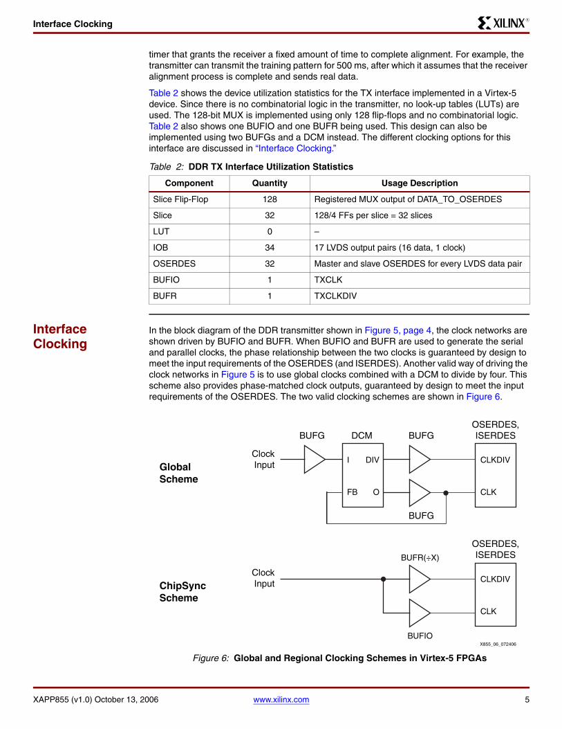
Interface Clocking
XAPP855 (v10) October 13 2006 wwwxilinxcom 5
R
timer that grants the receiver a fixed amount of time to complete alignment For example the transmitter can transmit the training pattern for 500 ms after which it assumes that the receiver alignment process is complete and sends real data
Table 2 shows the device utilization statistics for the TX interface implemented in a Virtex-5 device Since there is no combinatorial logic in the transmitter no look-up tables (LUTs) are used The 128-bit MUX is implemented using only 128 flip-flops and no combinatorial logic Table 2 also shows one BUFIO and one BUFR being used This design can also be implemented using two BUFGs and a DCM instead The different clocking options for this interface are discussed in ldquoInterface Clockingrdquo
Interface Clocking
In the block diagram of the DDR transmitter shown in Figure 5 page 4 the clock networks are shown driven by BUFIO and BUFR When BUFIO and BUFR are used to generate the serial and parallel clocks the phase relationship between the two clocks is guaranteed by design to meet the input requirements of the OSERDES (and ISERDES) Another valid way of driving the clock networks in Figure 5 is to use global clocks combined with a DCM to divide by four This scheme also provides phase-matched clock outputs guaranteed by design to meet the input requirements of the OSERDES The two valid clocking schemes are shown in Figure 6
Table 2 DDR TX Interface Utilization Statistics
Component Quantity Usage Description
Slice Flip-Flop 128 Registered MUX output of DATA_TO_OSERDES
Slice 32 1284 FFs per slice = 32 slices
LUT 0 ndash
IOB 34 17 LVDS output pairs (16 data 1 clock)
OSERDES 32 Master and slave OSERDES for every LVDS data pair
BUFIO 1 TXCLK
BUFR 1 TXCLKDIV
Figure 6 Global and Regional Clocking Schemes in Virtex-5 FPGAs
BUFR(divideX)
BUFIO
DIVI
OFB
CLKDIV
CLK
OSERDESISERDES
ClockInputGlobal
Scheme
ClockInputChipSync
Scheme
DCMBUFG BUFG
BUFG
CLKDIV
CLK
OSERDESISERDES
X855_06_072406
Interface Clocking
XAPP855 (v10) October 13 2006 wwwxilinxcom 6
R
Which clocking scheme is the best to use The BUFIOBUFR networks maximize performance at the expense of some convenience BUFIO and BUFR are regional clocks that cannot span the entire chip like a global clock This difference means that transferring data between the regional and global domains must be a part of the designers task and can simply mean adding a FIFO between the clock domains
Global clocks have lower performance than BUFIO but are more convenient to use If a clock is placed on a global network it can reach any component in the entire device To show the performance advantage of BUFIO Table 3 shows snapshots of several timing parameters some of which are included in the timing budget calculations for source synchronous interfaces In each case BUFIO has an advantage over BUFG and collectively those advantages are significant These parameters are used in the timing budget calculation section ldquoInterface Timing Budgetrdquo page 18 For the most current specifications always consult the data sheet on wwwxilinxcom
To offer the maximum performance the interface described in this application note uses a BUFIOBUFR clocking scheme in both the transmitter and receiver The interface does not include the FIFO logic necessary to transfer the parallel data tofrom the backend system domain However the BERT design discussed in ldquoIntroductionrdquo page 1 (see Figure 2 page 2) shows how to transfer data tofrom the RX and TX clock domains by using a FIFO18_36 primitive
Table 3 Comparison of Global and IO Clock Performance by Speed Grade
-3 -2 -1 Units
Maximum Frequency
BUFG max frequency 550 500 450 MHz
BUFIO max frequency 710 710 644 MHz
Duty Cycle Distortion
BUFG DYCD 150 150 150 ps
BUFIO DYCD 100 100 100 ps
Sampling Error
BUFG TSAMP 450 500 550 ps
BUFIO TSAMP 350 400 450 ps
Clock Tree Skew
BUFG skew for XC5VLX50T 270 270 270 ps
BUFIO skew for all devices 50 50 50 ps
DDR Receiver
XAPP855 (v10) October 13 2006 wwwxilinxcom 7
R
DDR Receiver The DDR receiver consists of three core modules DDR_8TO1_16CHAN_RX BIT_ALIGN_MACHINE and RESOURCE_SHARING_CONTROL The receiver is more complex than the DDR transmitter because it includes a dynamic alignment algorithm implemented in the FPGA fabric The DDR_8TO1_16CHAN_RX module takes 16 channels of data on the serial side optimizes the timing relationship of each channel with the clock performs 18 deserialization and presents 128 bits of data on the parallel side The port list is shown in Table 4
Table 4 DDR_8TO1_16CHAN_RX Module Port Definitions
Port Name IO Definition
DATA_RX_P [150] Input 16 data channels (P)
DATA_RX_N [150] Input 16 data channels (N)
CLOCK_RX_P Input Forwarded clock (P)
CLOCK_RX_N Input Forwarded clock (N)
INC_PAD Input Pulsing this pin causes the IDELAY tap setting of all data channels to increment by 1
DEC_PAD Input Pulsing this pin causes the IDELAY tap setting of all data channels to decrement by 1
DATA_FROM_ISERDES [1270] Output Parallel side data to backend system
RESET Input Reset synchronous to the RX domain
IDLY_RESET Input Reset synchronous to the RX domain that only resets the IDELAY tap settings of all data channels
IDELAYCTRL_RESET Input Reset synchronous to the TX domain that only resets the IDELAYCTRL module
BITSLIP_PAD Input Pulsing this pin causes one bitslip operation on all data channels
CLK200 Input Reference clock to IDELAYCTRL module
TAP_00 TAP_01 TAP_03 TAP_04 TAP_05 TAP_06 TAP_07 TAP_08 TAP_09 TAP_10 TAP_11 TAP_12 TAP_13 TAP_14 TAP_15
Output[50] Each of these 6-bit signals contains the current IDELAY tap value of the sixteen data channels Possible values 0-63
TAP_CLK [50] Output The 6-bit signal containing the current IDELAY tap value of the clock channel Permanently set to zero because the clock channel is not adjusted
TRAINING_DONE Output Flag indicating alignment is complete
RXCLK Output RX Source Sync Clock
RXCLKDIV Output RX Source Sync Clock divided by 4
IDELAY_READY Output Flag indicating IDELAYCTRL is calibrated
DDR Receiver
XAPP855 (v10) October 13 2006 wwwxilinxcom 8
R
Most of the logic used in the receiver is contained within the ISERDES The ISERDES is part of the ChipSync technology and is found in IO of all Virtex-5 devices The ISERDES can be programmed to do any deserialization up to 110 and do single or double data rate reception For deserializations greater than 61 a second ISERDES is needed (taken from the second IO in the LVDS pair) The first ISERDES is called the master and the second ISERDES is called the slave Figure 7 shows a single channel of the RX
Figure 7 MasterSlave ISERDES Pair for a Single Data Channel with 18 Deserialization
MasterISERDES
Serial DataExternal to
FPGA
X855_07_080306
Parallel Datainto FPGA Fabric
SlaveISERDES
SHIFTOUT2SHIFTOUT1
SHIFTIN2SHIFTIN1
Q1
Q2
Q3
Q4
Q5
Q6
Q1
Q2
Q3
Q4
Q5
Q6
Data8
Data7
Data6
Data5
Data4
Data3
Data2
Data1
DDR Receiver
XAPP855 (v10) October 13 2006 wwwxilinxcom 9
R
The receiver interface (Figure 8) consists of 16 masterslave ISERDES pairs Since this interface is source synchronous the clock source comes from the transmitter The clock is buffered in the receiver by a BUFIO component and divided to the parallel clock rate by a BUFR component
Figure 8 Block Diagram of RX Interface
MasterDATA_RX_P[00]
DATA_RX_N[00]
LVDS_25
Slave
IODELAY
CHAN_SELDATA_ALIGNED
DATA_TO_MACHINE
RXCLK(1)
START_ALIGN
Master
LVDS_25
Slave
ISERDES_CH_01 IODELAY
X855_08_082806
DQ
BUFIO
BUFR (divide4)
8 [72]
[10]
[98]
[1510]
[127122]
[121120]
4
8
8 8
3
3
3
DATA_RX_P[01]
DATA_RX_N[01]
Master
LVDS_25
Slave
IODELAY
DATA_RX_P[15]
DATA_RX_N[15]
ISERDES_CH_15
ISERDES_CH_00
RXCLKDIV
INC
ICE
BITSLIP
RXCLKDIV(1)
INC ICEBITSLIP
To CH 15
To CH 01
To CH 00
RX_IDELAYCTRL
Resource SharingControl
Bit AlignMachine
200 MHzSource
LVDS_25
CLOCK_RX_N
CLOCK_RX_P
Notes1 RXCLK and RXCLKDIV drive all ISERDES both master and slave
IODELAY
Fixed to Tap 0
Decoder
DDR Receiver
XAPP855 (v10) October 13 2006 wwwxilinxcom 10
R
Each ISERDES in Figure 8 page 9 contributes 8 bits to the 128-bit parallel data bus Since there is only one instance of BIT_ALIGN_MACHINE in the receiver each data channel must be aligned separately by sharing that resource The 8-bit data buses from each ISERDES are fed into a MUX which selects which of the 16 channels has access to the BIT_ALIGN_MACHINE resource RESOURCE_SHARING_CONTROL controls the MUX to ensure that every channel completes its alignment before the MUX switches to the next channel The START_ALIGN signal tells the BIT_ALIGN_MACHINE that alignment can begin on the current channel because the MUX output is stable The DATA_ALIGNED signal tells the RESOURCE_SHARING_CONTROL module that alignment on the current channel is complete
The order of the parallel data outputs of the ISERDES is the opposite of the parallel data inputs of the OSERDES The least significant OSERDES data inputs are fed into the master while the least-significant ISERDES data outputs come from the slave (Figure 4 page 3 versus Figure 7)
The IDELAYCTRL module in Figure 8 is shown as having no connection to the rest of the receiver Actually IDELAYCTRL is required to calibrate the IODELAY blocks in the path of each data channel A single IDELAYCTRL block is sufficient to calibrate all 16 data channels since all channels are in the same bank
The BIT_ALIGN_MACHINE generates three control signals that adjust the timing of the appropriate ISERDES INC and ICE cause the IODELAY to increment or decrement the delay in the datapath by a fixed amount of ~75 ps (if a 200 MHz reference clock is used) BITSLIP causes each ISERDES to rotate the order of the parallel output data bits facilitating the process of word alignment These three control signals are directed to the appropriate ISERDES by the decoder shown in Figure 8 Although not shown in the figure the decoder is also controlled by the RESOURCE_SHARING_CONTROL module
Table 5 shows the device utilization statistics for the RX interface implemented in a Virtex-5 device These figures exclude the counters used to track the IODELAY settings on all data channels in most instances those counters can be removed after the interface is integrated and verified in a specific environment The majority of the LUTs utilized are consumed by the BIT_ALIGN_MACHINE which is the core of the receiver alignment algorithm As in the TX interface the RX interface consumes one BUFIO and one BUFR for clocking The clocking could also be accomplished using BUFGs and a DCM as described in ldquoInterface Clockingrdquo page 5 but the performanceconvenience trade off would need to be considered
Table 5 DDR RX Interface Utilization Statistics
Component Quantity Usage Description
Slice Flip-Flop 131 Multiple uses
Slice 105 Multiple uses
LUT 263 Multiple uses
IOB 34 17 LVDS input pairs (16 data 1 clock)
ISERDES 32 Master and slave ISERDES for every LVDS data pair
BUFIO 1 RXCLK
BUFR 1 RXCLKDIV
Receiver Interface Dynamic Timing
XAPP855 (v10) October 13 2006 wwwxilinxcom 11
R
Receiver Interface Dynamic Timing
The timing of the receiver interface is broken into two parts
bull The suboptimal timing inherent in the data and clock paths
bull The optimal timing created by the receiver when adjusting dynamic delays on each of the 16 data channels
Inherent Timing
An inventory of all propagation delays in the clock and datapaths must be taken to derive the inherent setuphold times The clock and datapaths for a single channel of this interface are shown in Figure 9 The ISE Timing Analyzer breaks down the paths into the timing parameters shown All components in the path have both a minimum and maximum value to account for process variations
Figure 10 page 12 shows the timing analyzer settings used to generate the information in this report Each of the timing parameters is described in Table 6 page 12 and Table 7 The minimum and maximum values of the individual timing parameters for the clock and datapaths are shown in Table 8 and Table 9 page 13
Note All raw timing numbers referenced in this document are subject to minor changes in subsequent revisions of the ISE tools
Figure 9 Timing Components of RX Data and Clock Paths
ISERDESFFsIODELAY
VariableInit to 0
DI O
CLK
IODELAYIBUFDS
IBUFDS
+
ndash
+
ndash Fixed toTap 0
I O
X855_09_082806
DataPath
ClockPath
TIOPI TIODDO_IDATAINTNET1 TNET2
TIOPI TIODDO_IDATAIN TISDCK_DDLY
TBUFIOCKO_O
BUFIO
Receiver Interface Dynamic Timing
XAPP855 (v10) October 13 2006 wwwxilinxcom 12
R
Figure 10 ISE Timing Analyzer Properties Used in this Document
Table 6 Datapath Timing Definitions
Timing Parameter Description
TIOPI Delay from the IOB pad through the LVDS input buffer to the I pin of the IOB pad
TIODDO_IDATAIN Delay from the I pin of IOB pad to the D input of the ISERDES
TISDCK_DDLY Delay from the D input of the ISERDES to the sampling registers in the ISERDES (setup and hold times of ISERDES)
Table 7 Clock Path Timing Definitions
Timing Parameter Description
TIOPI Delay from the IOB pad through the LVDS input buffer to the I pin of the IOB pad
TIODDO_IDATAIN Delay from I pin of IOB pad to the O output of the IODELAY block
TNET1 Delay from the O output of the IODELAY block to the I pin of BUFIO
TBUFIOCKO_O Clock to out delay of BUFIO
TNET2 Clock distribution delay from BUFIO output to the clock input of data ISERDES
Table 8 Datapath Delay Inventory for a -1 Speed Grade XC5VLX50T Device
Timing Parameter Maximum Datapath Delay Minimum Datapath Delay
TIOPI 1083 ns 0763 ns
TIODDO_IDATAIN 0671 ns 0671 ns
TISDCK_DDLY 0064 ns ndash0038 ns
TOTAL 1818 ns 1396 ns
XAPP855_10_071306
Receiver Interface Dynamic Timing
XAPP855 (v10) October 13 2006 wwwxilinxcom 13
R
According to the inherent timing prediction the data is going to arrive before the clock by an amount determined by Equation 1 and Equation 2 Equation 1 calculates that data arrives before the clock by at least 1076 ns in a -1 device Equation 2 calculates that data arrives before the clock by at most 2213 ns Equation 3 shows a timing window that covers all -1 devices under all conditions This timing window describes the inherent timing of the data and clock paths Assuming skew-matched PCB traces for all sixteen channels then it can be assumed that all 16 channels in the receiver have roughly the same timing window
Equation 1
Equation 2
Equation 3
Figure 11 shows the timing windows for all speed grades of an XC5VLX50T device as well as a hardware measurement of the inherent timing relationship (to validate the calculations) The hardware measurement shows the DDR interface data arriving 1425 ns before the clock which by inspection places the device in all three speed grade ranges (the device used for the hardware measurement is a -2 device)
Table 9 Clock Path Delay Inventory for a -1 Speed Grade XC5VLX50T Device
Timing Parameter Maximum Clock Path Delay Minimum Clock Path Delay
TIOPI 1150 ns 0820 ns
TIODDO_IDATAIN 0671 ns 0671 ns
TNET1 0254 ns 0190 ns
TBUFIOCKO_O 1130 ns 0894 ns
TNET2 0404 ns 0319 ns
TOTAL 3609 ns 2894 ns
Setup Time Max Data Delay Min Clock Delay 1818 2894ndash 1076 nsndash==ndash=
Hold Time Max Clock Delay Min Data Delay 3609 1396ndash 2213 ns==ndash=
Timing Window 2213 1076ndash 1137 ns==
Figure 11 Timing Windows Show Uncertainty in ClockData Relationship as Calculated by Timing Analyzer
400 Mbs Data (T = 25 ns)
1425 ns Hardware MeasurementData Arrives
x855_11_091806
-11076ns 2213 ns
-21043 ns 2039 ns
-30989 ns 1878 ns
Receiver Interface Dynamic Timing
XAPP855 (v10) October 13 2006 wwwxilinxcom 14
R
Dynamic Timing and BIT_ALIGN_MACHINE
In ldquoInherent Timingrdquo page 11 the inherent timing of the interface was calculated for all speed grades and validated with a hardware measurement In that case the inherent timing was sufficient because the data rate is only 400 Mbs (Figure 11 page 13) What happens when the data rate is increased such that the hold edge of the data window begins to shrink (Figure 12)
At 600 Mbs the inherent timing relationship is no longer adequate to meet timing because there are cases when the sampling clock edge is in the middle of the data transition As the data rates increase to 800 and 1000 Mbs the clock actually captures the data arriving one bit time later For designs that are sensitive to word alignment this is unacceptable
The solution to the suboptimal inherent timing is dynamic timing The BIT_ALIGN_MACHINE module in the receiver performs two functions of dynamic timing
bull Bit Alignment Position the sampling edge of the clock at the center of the data eye by adding delay to the datapaths
bull Word Alignment Ensure that the parallel data bits are in the correct order at the output of the ISERDES by using the bitslip function in the ISERDES
The steps of the bit-alignment procedure are shown in Figure 13 page 15 Each step of the algorithm can either add or subtract delay from the datapath All 16 channels are taken through this procedure independently This procedure measures one full data eye (in terms of 75 ps delay taps) and then returns to the center of the data eye Steps 1 and 2 are dedicated to moving through the partial eye of the initial timing while steps 3 and 4 are dedicated to measuring a full eye Step 5 is dedicated to positioning the clock edge at the center of the data eye
Figure 12 Inherent Timing Windows Shown in Relation to Multiple Data Rates
400 Mbs Data (T = 25 ns)
600 Mbs Data (T = 167 ns)
800 Mbs Data (T = 127 ns)
1000 Mbs Data (T = 10 ns)
-11076ns 2213 ns
-21043 ns 2039 ns
-30989 ns
1425 ns
1878 ns
Hardware MeasurementData Arrives
x855_12_091806
Receiver Interface Dynamic Timing
XAPP855 (v10) October 13 2006 wwwxilinxcom 15
R
Jitter is represented in Figure 13 as multiple transition lines Accounting for jitter is a crucial part of the algorithm In step 2 the first data transition is found If there is no jitter then the eye measurement can begin instantly after finding the transition However when jitter is considered the algorithm must find the first transition move through the transition and then begin looking for the second transition If the algorithm does not move through the first transition intelligently it runs the risk of falsely detecting the second transition
Once bit alignment is complete the order of the data bits can be adjusted to achieve word alignment The bit-alignment procedure ensures that data is being sampled correctly but the order of the data can be a few bits off from where the receiver expects it to be To correct this the bitslip feature of the ISERDES is used to slip bit times until the proper alignment is found For this feature to be useful a training pattern must be generated by the transmitter (as discussed in ldquoDDR Transmitterrdquo page 3) that the receiver can use to determine the proper word alignment In this reference design the training pattern is 00101100 (0x2C) This pattern is mostly arbitrary as many other patterns work just as well This pattern was chosen because a training pattern should behave electrically as much like real data as possible such that the center of the training eye is the center of the data eye Since real data contains strings of consecutive ones and zeros it is best for the training pattern to do the same For that reason a 0x2C pattern is better than an 0xAA pattern because it contains run lengths of 1 2 3 and 4 bit times
Table 10 page 16 shows the word-alignment process in the case where bit alignment completes with the data outputs set to 0x58 Since 0x58 is not the training pattern the receiver is looking for bitslip is asserted until 0x2C is found This reference design uses a 18 deserialization so there are only eight possible configurations of the parallel data outputs If bitslip is asserted infinitely the same eight configurations will repeat Bitslip in DDR mode is somewhat irregular because it does not simply rotate by one bit on every bitslip cycle This effect is inconsequential to the word-alignment procedure (see the Virtex-5 User Guide for more details)
Figure 13 Dynamic Bit-Alignment Procedure in BIT_ALIGN_MACHINE
Data 0
Data Arrives Before Clock
Data 1
x855_13_091806
Data 0 Data 1
Data 0 Data 1
Data 0 Data 1
Data 0 Data 1
Sampling Clock (Fixed Delay)
Return to Center of Eye
End Measuring Eye
Begin Measuring Eye
Find 1st Transition
Initial Timing1
2
3
4
5
Receiver Interface Dynamic Timing
XAPP855 (v10) October 13 2006 wwwxilinxcom 16
R
The FSM in the BIT_ALIGN_MACHINE module used to implement both bit and word alignment is shown in Figure 14 page 17 The FSM is divided into five sections loosely described as finding the first transition getting through the first transition finding the second transition returning to the center of the eye and word alignment
To get through the first transition effectively for all possible types of jitter two methods are used The first method pertains to random jitter If there is a lot of random jitter at the sampling point then the samples generated are not stable The algorithm detects this instability by comparing current samples to older samples and therefore knows where the transition begins and ends But what if the jitter is extremely deterministic The transition then has discreet crossing points such that within the transition there is very stable but incorrect data In this case the algorithm does not sense any instability and falsely concludes that the sampling point is not in the transition To address this case apart from evaluating stability the algorithm also evaluates the correctness of the data content by using the bitslip feature in the middle of the transition For example if the algorithm determines that the sampled data is stable it then asserts bitslip to look for the correct data If 0x2c is found within eight assertions of bitslip then the sampling point is not in the transition But if 0x2c is not found then the algorithm increments the data delay and repeats the transition test again
Table 10 Word Alignment in the DDR Receiver
Bitslip Cycle Data Value (Hex) Data Value (Bin) Description of Bitslip operation
1 58 0101 1000 ndash
2 0B 0000 1011 Rotate 3 bits to right
3 16 0001 0110 Rotate 1 bit to left
4 C2 1100 0010 Rotate 3 bits to right
5 85 1000 0101 Rotate 1 bit to left
6 B0 1011 0000 Rotate 3 bits to right
7 61 0110 0001 Rotate 1 bit to left
8 2C 0010 1100 Rotate 3 bits to right
Receiver Interface Dynamic Timing
XAPP855 (v10) October 13 2006 wwwxilinxcom 17
R
Figure 14 FSM in the BIT_ALIGN_MACHINE Module
TRANSITION_CHECK (01000)
First TransitionNot Detected
First TransitionNot Detected
First TransitionDetected
First TransitionDetected
Past the FirstTransition
Second TransitionNot Detected
Second TransitionDetected
Decrement DelayAgain
Bit AlignmentComplete
Still Samplingin Transition
INC_ONCE (01111)
SEARCH_PAT (01101)
IDLE (01100)
IDLE (10000)
RECHECK_TRANS (00010)
ONE_BITSLIP (00110)
INC_ONCE (01011)
WAIT_8_CYCLES (00100)
COUNT_1 (01110)
INC_ONCE (01001)
WAIT_8_CYCLES (00011)
IDLE (10010)
TRAINING_DONE (00111)
FIRST_SAMPLE (00001)
RESET (00000)
DEC_TO_HALF (01010)
WORD_ALIGN (00101)
X855_14_082806
Routine to Avoid False Detection of Second Transition
=CHECK_PATTERN
Receiver Interface Dynamic Timing
XAPP855 (v10) October 13 2006 wwwxilinxcom 18
R
Interface Timing Budget
In addition to sampling the data as closely as possible to the center of the data eye the actual size of the data eye is important By accurately predicting the size of the data eye in the receiver the overall performance ceiling of the interface can be inferred The ideal data eye width is the period of the data rate (for example TBit_Period = 100 ns for 1000 Mbs) Both the transmitter and receiver circuits have sources of error that subtract from the ideal data eye The equation for the eye width at the output of the transmitter is shown in Equation 4 TJITTER is the peak-to-peak jitter of the clock source driving the transmitter data bus and forwarded clock TDCD is the maximum duty cycle distortion of the clock tree driving the data bus and forwarded clock Skew is not considered in the transmitter or receiver because the receiver calibrates out skew between channels by performing alignment on each channel individually
Equation 4
Equation 5 calculates the width of the data eye at the receiver flip-flops Ideally the eye width at the receiver is the same as the eye width at the output of the transmitter but there are sources of error in the transmission medium and receiver circuitry Duty cycle distortion must be considered again on the receiver clock tree TSAMP_BUFIO is the receiver sampling error due to drift caused by voltage and temperature variations TIDELAYPAT_JIT is the amount of pattern dependent jitter that is accumulated in each tap of the IDELAY chain For a clock pattern TIDELAYPAT_JIT is 0 pstap peak to peak For a data pattern with long and short run lengths of zeroes and ones (simulated by PRBS23) TIDELAYPAT_JIT is a finite value that must be considered in the timing budget
Equation 5
TBOARD_JITTER includes jitter induced by receiver input capacitance and the parasitics of the physical data path on the PCB TBOARD_JITTER must be determined by simulation as it varies as a function of frequency and for receivers of different types and vendors On the ML550 with a -2 speed-grade Virtex-5 device the TBOARD_JITTER is measured at roughly 200 ps at 900 Mbs (assuming data content equivalent to PRBS23) TQUANTIZATION_ERR or quantization error is caused by the granularity of the IDELAY tap chain Working with 75 ps increments it is not possible to utilize the entire data eye since inevitably some valid eye width is lost between two taps The value for this loss is 75 ps As long as the receiver eye width calculated using Equation 5 is greater than or equal to 0 the interface operates correctly over process voltage and temperature
For example Equation 6 and Equation 7 show the timing budget calculation for the DDR interface running at 900 Mbs in a -2 speed grade device on an ML550 evaluation board Refer to the data sheet for the most current values The TX interface is looped back to the RX interface on the same Virtex-5 FPGA as shown in Equation 2
Equation 6
Equation 7
Changes in voltage and temperature cause the data channels of the interface to drift relative to the clock If the DDR interface were to transfer user data for a long period of time over all specified conditions of temperature and voltage Equation 7 states that there would be at least 107 ps (one or two IDELAY taps) of data window remaining valid during all fluctuations of temperature and voltage Compare this calculation to the measurements in Table 12 page 21 Case 900 Mbs There are four taps that are error free under all conditions In ldquoAppendixrdquo there are three -2 devices tested at 900 Mbs and each has 4 4 and 3 taps respectively that are error free under all conditions
DATA_EYE_WIDTH_TX TBIT_PERIOD TJITTERndash TDCD_BUFIOndash=
DATA_EYE_WIDTH_RX DATA_EYE_WIDTH_TX
TBOARD_JITTER
ndash
TSAMP_BUFIOndash TDCD_BUFIOndash
TIDELAYPAT_JIT IDELAY taps in datapathtimes[ ]ndash
TQUANTIZATION_ERRndash
=
DATA_EYE_WIDTH_TX 1111 ps 25 psndash 100 psndash 986 ps= =
DATA_EYE_WIDTH_RX986 ps 200 psndash 400 psndash 100 psndash 8 ps 13 tapstimes[ ] 75 ps 107 ps=ndashndash
=
Interface Characterization
XAPP855 (v10) October 13 2006 wwwxilinxcom 19
R
At a given temperature and voltage setting the data valid window is much larger because there is no drift when temperature and voltage are constant The size of the data valid window under constant conditions is 107 ps + TSAMP_BUFIO which in this case is at least 507 ps (six or seven IDELAY taps) Compare this calculation to the measurements of any single condition in Table 12 Case 900 Mbs In the worst case (ndash5 supply) there are 7 taps that are error free
Equation 8 and Equation 9 show the same timing budget calculation for the DDR interface running at 10 Gbs in a -2 speed grade device on an ML550 Evaluation Board
Equation 8
Equation 9
Equation 9 predicts that no data window remains valid during all specified fluctuations of temperature and voltage (compare to Table 12 Case 1000 Mbs) In ldquoAppendixrdquo there are three -2 devices tested at 1000 Mbs and each has 1 3 and 1 taps respectively that are error free under all conditions This data rate and device combination are very marginal cases
To operate at 10 Gbs the DDR interface requires additional circuitry to track out voltage-temperature variations in real-time (see XAPP860 16-channel DDR LVDS Interface with Real-time Window Monitoring for a DDR Interface with real-time window monitoring) If the voltage-temperature variations are removed from the picture the predicted data valid window is ndash120 ps + TSAMP_BUFIO which in this case is at least 280 ps (3 or 4 taps) Compare this calculation to the measurements of any single condition in Table 18 page 34 There are at least four error-free taps in all conditions
Interface Characterization
By following the procedure illustrated in Figure 13 page 15 the bit-alignment algorithm should never insert more than approximately 15 bit times of delay on the data channels The fewest number of delay taps should be used in the datapath because they produce a finite amount of degradation (TIDELAYPAT_JIT) The worst-case initial timing for the algorithm occurs when the clock samples just before the data transitions as in the 600 Mbs case in Figure 12 page 14 The algorithm must move all the way through the first eye to find the first transition (1 bit time) and then move halfway into the next eye to center the sampling point (05 bit time) This process produces a worst-case total delay insertion of 15 bit times
The actual performance of the bit-alignment algorithm is characterized as a function of data rate in Figure 15 page 20 For all data rates the expectation is that the tap settings of all 16 channels in the DDR receiver do not exceed approximately 15 bit times of delay Both the maximum and minimum tap setting of all 16 channels is recorded for each data rate This graph only shows the data for a single device Comparing the 15 bit time mask to the actual settings it is clear that the algorithm remains within the 15 bit time limit At 13 Gbs the tap setting actually exceeds the mask by one tap (a negligible violation)
DATA_EYE_WIDTH_TX 1000 ps 25 psndash 100 psndash 875 ps= =
DATA_EYE_WIDTH_RX 875 ps 300 psndash400 ps 100 psndash
ndash8 ps 15 tapstimes[ ] 75 ps 120 psndash=ndashndash
=
Interface Characterization
XAPP855 (v10) October 13 2006 wwwxilinxcom 20
R
The maximum and minimum tap settings in Figure 15 generally stay within 3 to 4 taps of each other except in the case of 640 Mbs and 1300 Mbs data rates These data rates are seams in the inherent timing At data rates below 640 Mbs the tap settings are in the range of 30 taps and at data rates above 640 Mbs the tap settings are in the range of 12 taps Referring back to Figure 12 page 14 it is clear why this seam occurs As the data rate increases past 600 Mbs the initial sampling point of the inherent timing moves into a different data eye creating a different starting point for the algorithm At 640 Mbs some of the 16 channels start in one eye while other channels start in the other eye Fortunately this is not an issue because the single bit time of difference between the channels is resolved using bitslip
Referring back to Figure 8 page 9 the clock channel goes through an IDELAY block with a default value of 0 Once the data rate is chosen for a given design this initial IDELAY value can be changed to a non-zero value to achieve more favorable inherent timing For example a design running at 620 Mbs can use 30 IDELAY taps on the delay channels each contributing a certain amount of jitter to the timing budget calculation By setting the initial clock delay to 5 taps the inherent timing moves across the seam shown in the 600 Mbs range of Figure 15 causing the data channels to only use about 12 IDELAY taps Only spectrally rich data patterns accumulate jitter in the IDELAY tap chain so the clock IDELAY can be set to any value without diminishing the timing budget This optimization is entirely optional and can be done once the design is running in hardware
The DDR receiver is designed to remove skew between channels by aligning each channel individually The ML550 board on which this reference design is characterized is designed to have minimal skew between channels However there is clearly a finite amount of skew between channels due to clock skew in the TX and RX BUFIO networks package skew and trace length tolerance on the ML550 board Table 11 page 21 shows how the bit-alignment algorithm sets the delay for each channel differently to compensate for skew between channels The table captures the range of settings among the 16 channels at specific data rates for a -2 device If there were additional skew among the 16 channels then the tap setting range would be larger to compensate for it The algorithm is designed such that skew between channels should not diminish the performance of the interface The range of tap settings differs for different devices and speed grades but the magnitude should be approximately the same
Figure 15 Bit-Alignment Algorithm Performance
60
50
40
30
20
10
0200 400 600 800 1000 1200 1400 1600
Data Rate (Mbs)
Del
ay T
ap U
tiliz
atio
n HW Measurement (Min)HW Measurement (Max)15 Bit Time Mask
X855_15_072406
Interface Characterization
XAPP855 (v10) October 13 2006 wwwxilinxcom 21
R
Since the receiver alignment logic only runs once immediately after reset the resulting dynamic timing must be adequate to ensure error-free operation over the specified voltage and temperature variations that can occur over time The data-valid window at the receiver input must be wide enough to withstand these variations (receiver drift) Table 12 page 21 shows the data-valid window at the ISERDES registers in the DDR receiver The eyes shown are collective eyes of all 16 channels The BERT testbench configuration loops back the DDR transmitter to the DDR receiver Using pattern generators and error detectors programmed to send and receive a pseudorandom bit sequence (PRBS23) the width of the data-valid window is evaluated using pseudorandom data that closely resembles real user data
Table 11 Tap Setting Range For Various Data Rates Measured on a -2 Device
Data Rate (Mbs) Tap Setting Range Compensated Skew
500 31ndash34 4 taps
600 28ndash30 3 taps
700 10ndash12 3 taps
800 11ndash13 3 taps
900 11ndash13 3 taps
1000 13ndash15 3 taps
1100 13ndash15 3 taps
1200 14ndash15 2 taps
Table 12 Measurement of Receiver Drift under Extreme Conditions for Multiple Data Rates
ConditionIODELAY Taps (1)
ndash8 ndash7 ndash6 ndash5 ndash4 ndash3 ndash2 ndash1 0 +1 +2 +3 +4 +5 +6 +7 +8
Case 800 Mbs
25degC Nom Supplies F F F P P P P P C P P P P P F F F
0degC Nom Supplies F F F P P P P P P P P P P P F F F
85degC Nom Supplies F F F P P P P P P P P P P P F F F
25degC +5 Supplies F P P P P P P P P P P P F F F F F
0degC +5 Supplies F P P P P P P P P P P P F F F F F
85degC +5 Supplies F P P P P P P P P P P P F F F F F
25degC ndash5 Supplies F F F F F F P P P P P P P P P F F
0degC ndash5 Supplies F F F F F F P P P P P P P P P P F
85degC ndash5 Supplies F F F F F P P P P P P P P P P F F
CONCLUSION Error free under all conditions when calibrated under nominal conditions to position C
Interface Characterization
XAPP855 (v10) October 13 2006 wwwxilinxcom 22
R
Case 900 Mbs
25degC Nom Supplies F F F F P P P P C P P P P F F F F
0degC Nom Supplies F F F F P P P P P P P P P F F F F
85degC Nom Supplies F F F F P P P P P P P P F F F F F
25degC +5 Supplies F F P P P P P P P P P F F F F F F
0degC +5 Supplies F F P P P P P P P P P F F F F F F
85degC +5 Supplies F F P P P P P P P P P F F F F F F
25degC ndash5 Supplies F F F F F F F P P P P P P P P F F
0degC ndash5 Supplies F F F F F F F P P P P P P P P F F
85degC ndash5 Supplies F F F F F F F P P P P P P P F F F
CONCLUSION Error free under all conditions when calibrated under nominal conditions to position C
Case 1000 Mbs
25degC Nom Supplies F F F F F P P P C P P P F F F F F
0degC Nom Supplies F F F F F P P P P P P P F F F F F
85degC Nom Supplies F F F F F P P P P P P P F F F F F
25degC +5 Supplies F F F P P P P P P P F F F F F F F
0degC +5 Supplies F F F P P P P P P P F F F F F F F
85degC +5 Supplies F F F P P P P P P P P F F F F F F
25degC ndash5 Supplies F F F F F F F F P P P P P P F F F
0degC ndash5 Supplies F F F F F F F F P P P P P P F F F
85degC ndash5 Supplies F F F F F F F F P P P P P P F F F
CONCLUSION Error free under all conditions when calibrated under nominal conditions to position C
Case 1100 Mbs
25degC Nom Supplies F F F F F P P P C P F F F F F F F
0degC Nom Supplies F F F F F P P P P P F F F F F F F
85degC Nom Supplies F F F F F P P P P P F F F F F F F
25degC +5 Supplies F F F P P P P P P F F F F F F F F
0degC +5 Supplies F F F P P P P P P F F F F F F F F
85degC +5 Supplies F F F P P P P P P F F F F F F F F
25degC ndash5 Supplies F F F F F F F F P P P P F F F F F
0degC ndash5 Supplies F F F F F F F F P P P P F F F F F
85degC ndash5 Supplies F F F F F F F F P P P P F F F F F
CONCLUSION Error free under all conditions when calibrated under nominal conditions to position C
Table 12 Measurement of Receiver Drift under Extreme Conditions for Multiple Data Rates (Continued)
ConditionIODELAY Taps (1)
ndash8 ndash7 ndash6 ndash5 ndash4 ndash3 ndash2 ndash1 0 +1 +2 +3 +4 +5 +6 +7 +8
Interface Characterization
XAPP855 (v10) October 13 2006 wwwxilinxcom 23
R
In all test cases shown in Table 12 page 21 the bit-align machine accurately places the sampling point in the center of the data eye (indicated by the C in each test case) In the 1100 Mbs case the bit-align machine places the sampling point slightly off center This slight inaccuracy occurs when the center of a real data pattern diverges from the center of the training pattern The electrical behavior of different data patterns is discussed below
After the dynamic timing is established for a given test case under nominal conditions the device is subjected to extremes of temperature and voltage to stress the receiver timing At data rates of 1100 Mbs and below the dynamic timing established after reset under nominal conditions is sufficient to meet timing over all specified extreme conditions (the column with the C passes traffic error free under all conditions) At a data rate of 1200 Mbs the design operates correctly under nominal conditions but the data-valid window is not large enough to withstand the voltage variations For this particular transmission medium the 1200 Mbs case requires a real-time adjustment circuit that could track the center of the eye
The full datapath of the testbench consists of
TX rarr 5 FR-4 rarr SAMTEC QSE Conn rarr 12 Ribbon Cable rarr SAMTEC QSE Conn rarr 5 FR-4 rarr RX
For shorter transmission media higher performance can be achieved in accordance with the section ldquoInterface Timing Budgetrdquo page 18 Interface performance is not solely a question of the LVDS driver performance specification but rather a question of adequate timing margin to withstand production and environmental variations From Table 12 the total amount of variation experienced over temperature and voltage is roughly 375 ps (5 taps at 75 ps per tap) This number should be comparable to the specification for receiver sampling error (TSAMP_BUFIO) shown in the Virtex-5 Data Sheet
Case 1200 Mbs
25degC Nom Supplies F F F F F F P P C P F F F F F F F
0degC Nom Supplies F F F F F F P P P P F F F F F F F
85degC Nom Supplies F F F F F F P P P F F F F F F F F
25degC +5 Supplies F F F F P P P P F F F F F F F F F
0degC +5 Supplies F F F P P P P P F F F F F F F F F
85degC +5 Supplies F F F F P P P P F F F F F F F F F
25degC ndash5 Supplies F F F F F F F F F P P P F F F F F
0degC ndash5 Supplies F F F F F F F F F P P P F F F F F
85degC ndash5 Supplies F F F F F F F F F P P F F F F F F
CONCLUSION Errors caused by plusmn5 variations in supply voltages
Notes 1 Where 0 is the reference tap determined by the bit-align machine under nominal conditions at 25degC2 P = Error-free transmission F = Error in transmission C = IODELAY tap position selected by bit-align machine under nominal conditions at 25degC3 Device under test is -2 speed grade
Table 12 Measurement of Receiver Drift under Extreme Conditions for Multiple Data Rates (Continued)
ConditionIODELAY Taps (1)
ndash8 ndash7 ndash6 ndash5 ndash4 ndash3 ndash2 ndash1 0 +1 +2 +3 +4 +5 +6 +7 +8
Interface Characterization
XAPP855 (v10) October 13 2006 wwwxilinxcom 24
R
Pattern Dependence of Receiver Performance
Different types of data patterns have different electrical signatures (rise and fall times jitter eye symmetry etc) A pattern with very narrow spectral content (such as a clock pattern) moves very favorably through the link because the receiver frequency response has little effect on the signal integrity However a pattern with wide spectral content (such as real data and pseudorandom patterns) stresses the links frequency response If the frequency response is not flat across the entire spectrum of the data content then the signal integrity is degraded as a result The amount of degradation measured is shown in Table 13 page 25 The DDR transmitter is looped back to the DDR receiver and different patterns are programmed to traverse the link Performance is assessed by evaluating the integrity of those patterns in the receiver
PRBS7 is a pseudorandom data pattern with a maximum run length of seven consecutive zeroes or ones PRBS15 is defined as having a maximum run length of fifteen consecutive zeroes or ones These limitations on run lengths limit the spectral content of the pattern A PRBS15 pattern has greater spectral content than a PRBS7 pattern and therefore is a more strenuous test for the link PRBS29 is the most strenuous test in Table 13 A clock pattern is effectively a PRBS1
As predicted Table 13 shows that there is more degradation for data patterns with more spectral content At 1000 Mbs and below the data eye closure is symmetrical Symmetrical eye closure is desired because it does not change the center of the eye as determined by the bit-alignment algorithm Above 1000 Mbs the eye closure becomes more asymmetrical causing the center of the data eye to diverge from the calibrated center (by only 1 tap)
In every data rate shown in Table 13 all significant pattern-dependent degradation is caused between PRBS1 (clock pat) and PRBS15 Between PRBS15 and PRBS29 there is no additional degradation recorded in any of the measurements
Interface Characterization
XAPP855 (v10) October 13 2006 wwwxilinxcom 25
R
Table 13 Link Performance for Various Types of Data Measured on a -2 Device
PatternIODELAY Taps (1)
ndash8 ndash7 ndash6 ndash5 ndash4 ndash3 ndash2 ndash1 0 +1 +2 +3 +4 +5 +6 +7 +8 +9
Case 600 Mbs
Clock Pat (0101) P P P P P P P P C P P P P P P P P P
Training Pat (0x2C) P P P P P P P P C P P P P P P P P F
PRBS7 P P P P P P P P C P P P P P P P P F
PRBS15 F P P P P P P P C P P P P P P P F F
PRBS23 F P P P P P P P C P P P P P P P F F
PRBS29 F P P P P P P P C P P P P P P P F F
Case 800 Mbs
Clock Pat (0101) F F P P P P P P C P P P P P P F F F
Training Pat (0x2C) F F P P P P P P C P P P P P P F F F
PRBS7 F F P P P P P P C P P P P P F F F F
PRBS15 F F F P P P P P C P P P P P F F F F
PRBS23 F F F P P P P P C P P P P P F F F F
PRBS29 F F F P P P P P C P P P P P F F F F
Case 1000 Mbs
Clock Pat (0101) F F F P P P P P C P P P P P F F F F
Training Pat (0x2C) F F F P P P P P C P P P P F F F F F
PRBS7 F F F F P P P P C P P P F F F F F F
PRBS15 F F F F F P P P C P P P F F F F F F
PRBS23 F F F F F P P P C P P P F F F F F F
PRBS29 F F F F F P P P C P P P F F F F F F
Case 1200 Mbs
Clock Pat (0101) F F F F P P P P C P P P P F F F F F
Training Pat (0x2C) F F F F P P P P C P P P F F F F F F
PRBS7 F F F F F P P P C P F F F F F F F F
PRBS15 F F F F F F P P C F F F F F F F F F
PRBS23 F F F F F F P P C F F F F F F F F F
PRBS29 F F F F F F P P C F F F F F F F F F
Case 1400 Mbs
Clock Pat (0101) F F F F F F P P C P P P F F F F F F
Training Pat (0x2C) F F F F F P P P C P P F F F F F F F
PRBS7 F F F F F F F P C P F F F F F F F F
PRBS15 F F F F F F F P C F F F F F F F F F
PRBS23 F F F F F F F P C F F F F F F F F F
PRBS29 F F F F F F F P C F F F F F F F F F
Notes 1 Where 0 is the reference tap determined by the bit-align machine under nominal conditions at 25degC2 P = Error-free transmission F = Error in transmission C = IODELAY tap position selected by bit-align machine under nominal conditions at 25degC
Resetting the Interface
XAPP855 (v10) October 13 2006 wwwxilinxcom 26
R
Resetting the Interface
Several dependencies determine the order in which circuits should be reset in the interface The receiver cannot begin the alignment algorithm if the transmitter is not sending the training pattern The transmitter must be reset before the receiver and time must be allowed for the training pattern to propagate across the link before the receiver comes out of reset The receiver also cannot begin the alignment algorithm until IDELAYCTRL has recovered from reset which could takes hundreds of cycles The recommended reset timing for the interface is shown in Figure 16 This reset timing is implemented in the BERT testbench for this interface
The TX reset (RST_TX) is used to reset all TX circuitry and also IDELAYCTRL The IDELAYCTRL reset is asynchronous so driving it with RST_TX is acceptable The minimum pulse width of IDELAYCTRL reset is 50 ns (TIDELAYCTRL_RPW) For that reason resets are held High for 16 clock cycles The RX reset (RST_RX) is used to reset all RX circuitry and is asserted when the IDELAYCTRL READY flag goes High indicating that the IODELAY blocks are calibrated
The timing of the READY flag in Figure 16 is a potential hazard Most likely it is High during a TX reset because it takes many cycles for IDELAYCTRL to deassert the READY flag It is easy to make the mistake of resetting the receiver too early To avoid this hazard the RX reset should be asserted only after seeing a deassertion and reassertion of the READY flag
Conclusion Based on the design and characterization described in this document the 16-Channel DDR reference design operates to the performance targets in Table 14 under all conditions of process voltage and temperature However to meet these targets over voltage and temperature the timing budget must be guaranteed according to the analysis in ldquoInterface Timing Budgetrdquo See ldquoAppendixrdquo page 27 for further justification of the maximum performance recommendations in Table 14
Figure 16 Recommended Interface Reset Timing
RST_TX
IDELAYCTRLREADY
RST_RX
16 Cycles X855_16_072406
Table 14 Performance of 16-Channel DDR Interface
Speed Grade Maximum Performance
-1 800 Mbs
-2 900 Mbs
-3 10 Gbs(1)
Notes 1 To achieve higher performance (up to 125 Gbs) see 16-channel DDR LVDS Interface with Realtime
Window Monitoring for an example of a DDR interface with real-time window monitoring
Appendix
XAPP855 (v10) October 13 2006 wwwxilinxcom 27
R
Appendix Performance Characterization Data
Refer to ldquoInterface Characterizationrdquo page 19 for explanations about how to interpret the data in the ldquoAppendixrdquo These tables show collective data eyes for the entire interface over process voltage and temperature (PVT) Three devices from each speed grade were selected for this characterization
The calibrated center position of the eye (marked by the C in the tables below) varies slightly from channel to channel (due to small skews between channels) That range is referred to as center tap range Analysis of Table 16 page 28 through Table 20 page 40 shows that the center tap range for slow and fast parts differ significantly at the same data rate (because the BIT_ALIGN_MACHINE algorithm adjusts for differences in speed)
All data in the ldquoAppendixrdquo is collected using the BERT testbench shown in Figure 2 page 2 The data pattern is PRBS23 and the devicepackage is XC5VLX50T-FF1136 The transmission path for the cases shown in Table 16 through Table 20 is repeated for convenience
TX rarr 5 FR-4 rarr SAMTEC QSE Conn rarr 12 Ribbon Cable rarr SAMTEC QSE Conn rarr 5 FR-4 rarr RX
A summary of these characterization results is shown in Table 15 Each of the nine parts were tested at 800 900 1000 1100 and 1200 Mbs When the interface is error free on all channels under all extreme conditions of temperature and voltage the particular test case is designated by a P A test case is marked FAIL when the interface suffered errors on any channel under any particular condition of voltage and temperature
Table 15 Summary of Interface Characterization Results
Device (SN) Speed Grade 800 Mbs 900 Mbs 1000Mbs 1100 Mbs 1200 Mbs
2194 -1 P P P FAIL FAIL
2219 -1 P FAIL FAIL FAIL FAIL
2199 -1 P P FAIL FAIL FAIL
001 -2 P P FAIL P FAIL
002 -2 P P P P FAIL
003 -2 P P FAIL FAIL FAIL
004 -3 P P P P P
005 -3 P P P P P
006 -3 P P P P P
Appendix
XAPP855 (v10) October 13 2006 wwwxilinxcom 28
R
Table 16 Measurement of Receiver Drift under Extreme Conditions at 800 Mbs
ConditionIODELAY Taps (1)
ndash8 ndash7 ndash6 ndash5 ndash4 ndash3 ndash2 ndash1 0 +1 +2 +3 +4 +5 +6 +7 +8
SN 2194 Speed Grade -1
25degC Nom Supplies F F F P P P P P C P P P P F F F F
0degC Nom Supplies F F F P P P P P P P P P P F F F F
85degC Nom Supplies F F F F P P P P P P P P P F F F F
25degC +5 Supplies F F P P P P P P P P P P F F F F F
0degC +5 Supplies F F P P P P P P P P P P F F F F F
85degC +5 Supplies F F P P P P P P P P P P F F F F F
25degC ndash5 Supplies F F F F F F P P P P P P P P P F F
0degC ndash5 Supplies F F F F F F P P P P P P P P P F F
85degC ndash5 Supplies F F F F F F P P P P P P P P P F F
Center Tap Range Taps 11ndash12
CONCLUSION Error free under all conditions when calibrated under nominal conditions to position C
SN 2219 Speed Grade -1
25degC Nom Supplies F F F P P P P P C P P P F F F F F
0degC Nom Supplies F F F P P P P P P P P P F F F F F
85degC Nom Supplies F F F P P P P P P P P P F F F F F
25degC +5 Supplies F P P P P P P P P P P F F F F F F
0degC +5 Supplies F P P P P P P P P P P F F F F F F
85degC +5 Supplies F P P P P P P P P P P F F F F F F
25degC ndash5 Supplies F F F F F F P P P P P P P P F F F
0degC ndash5 Supplies F F F F F F F P P P P P P P F F F
85degC ndash5 Supplies F F F F F F P P P P P P P P F F F
Center Tap Range Taps 13ndash16
CONCLUSION Error free under all conditions when calibrated under nominal conditions to position C
SN 2199 Speed Grade -1
25degC Nom Supplies F F F P P P P P C P P P P F F F F
0degC Nom Supplies F F F P P P P P P P P P P F F F F
85degC Nom Supplies F F F P P P P P P P P P P F F F F
25degC +5 Supplies F P P P P P P P P P P P F F F F F
0degC +5 Supplies F P P P P P P P P P P P F F F F F
85degC +5 Supplies F P P P P P P P P P P P F F F F F
25degC ndash5 Supplies F F F F F F P P P P P P P P P F F
0degC ndash5 Supplies F F F F F F P P P P P P P P P F F
85degC ndash5 Supplies F F F F F F P P P P P P P P P F F
Center Tap Range Taps 10ndash12
CONCLUSION Error free under all conditions when calibrated under nominal conditions to position C
Appendix
XAPP855 (v10) October 13 2006 wwwxilinxcom 29
R
SN 001 Speed Grade -2
25degC Nom Supplies F F F P P P P P C P P P P F F F F
0degC Nom Supplies F F F P P P P P P P P P P F F F F
85degC Nom Supplies F F F P P P P P P P P P P F F F F
25degC +5 Supplies F P P P P P P P P P P P F F F F F
0degC +5 Supplies F P P P P P P P P P P F F F F F F
85degC +5 Supplies F P P P P P P P P P P P F F F F F
25degC ndash5 Supplies F F F F F P P P P P P P P P P F F
0degC ndash5 Supplies F F F F F P P P P P P P P P P F F
85degC ndash5 Supplies F F F F F P P P P P P P P P P F F
Center Tap Range Taps 10ndash12
CONCLUSION Error free under all conditions when calibrated under nominal conditions to position C
SN 002 Speed Grade -2
25degC Nom Supplies F F F P P P P P C P P P P F F F F
0degC Nom Supplies F F F P P P P P P P P P P F F F F
85degC Nom Supplies F F F P P P P P P P P P P F F F F
25degC +5 Supplies F P P P P P P P P P P P F F F F F
0degC +5 Supplies F P P P P P P P P P P P F F F F F
85degC +5 Supplies F F P P P P P P P P P P F F F F F
25degC ndash5 Supplies F F F F F P P P P P P P P P P F F
0degC ndash5 Supplies F F F F F P P P P P P P P P P F F
85degC ndash5 Supplies F F F F F P P P P P P P P P P F F
Center Tap Range Taps 10ndash12
CONCLUSION Error free under all conditions when calibrated under nominal conditions to position C
SN 003 Speed Grade -2
25degC Nom Supplies F F F P P P P P C P P P P F F F F
0degC Nom Supplies F F F P P P P P P P P P P F F F F
85degC Nom Supplies F F F P P P P P P P P P P F F F F
25degC +5 Supplies F P P P P P P P P P P P F F F F F
0degC +5 Supplies F P P P P P P P P P P F F F F F F
85degC +5 Supplies F P P P P P P P P P P P F F F F F
25degC ndash5 Supplies F F F F F F P P P P P P P P P F F
0degC ndash5 Supplies F F F F F F P P P P P P P P P F F
85degC ndash5 Supplies F F F F F F P P P P P P P P P F F
Center Tap Range Taps 11ndash13
CONCLUSION Error free under all conditions when calibrated under nominal conditions to position C
Table 16 Measurement of Receiver Drift under Extreme Conditions at 800 Mbs (Continued)
ConditionIODELAY Taps (1)
ndash8 ndash7 ndash6 ndash5 ndash4 ndash3 ndash2 ndash1 0 +1 +2 +3 +4 +5 +6 +7 +8
Appendix
XAPP855 (v10) October 13 2006 wwwxilinxcom 30
R
SN 004 Speed Grade -3
25degC Nom Supplies F F F P P P P P C P P P P F F F F
0degC Nom Supplies F F F P P P P P P P P P F F F F F
85degC Nom Supplies F F F P P P P P P P P P P F F F F
25degC +5 Supplies F P P P P P P P P P P P F F F F F
0degC +5 Supplies F P P P P P P P P P P P F F F F F
85degC +5 Supplies F F P P P P P P P P P P F F F F F
25degC ndash5 Supplies F F F F F P P P P P P P P P F F F
0degC ndash5 Supplies F F F F F P P P P P P P P P F F F
85degC ndash5 Supplies F F F F F P P P P P P P P P F F F
Center Tap Range Taps 8ndash9 23ndash24
CONCLUSION Error free under all conditions when calibrated under nominal conditions to position C
SN 005 Speed Grade -3
25degC Nom Supplies F F P P P P P P C P P P P F F F F
0degC Nom Supplies F F P P P P P P P P P P P F F F F
85degC Nom Supplies F F F P P P P P P P P P P P F F F
25degC +5 Supplies F P P P P P P P P P P P F F F F F
0degC +5 Supplies F P P P P P P P P P P P F F F F F
85degC +5 Supplies F P P P P P P P P P P P F F F F F
25degC ndash5 Supplies F F F F P P P P P P P P P P P F F
0degC ndash5 Supplies F F F F P P P P P P P P P P P F F
85degC ndash5 Supplies F F F F P P P P P P P P P P P F F
Center Tap Range Taps 9ndash10
CONCLUSION Error free under all conditions when calibrated under nominal conditions to position C
SN 006 Speed Grade -3
25degC Nom Supplies F F P P P P P P C P P P P F F F F
0degC Nom Supplies F F P P P P P P P P P P P F F F F
85degC Nom Supplies F F F P P P P P P P P P P F F F F
25degC +5 Supplies F P P P P P P P P P P P F F F F F
0degC +5 Supplies F P P P P P P P P P P P F F F F F
85degC +5 Supplies F F P P P P P P P P P P F F F F F
25degC ndash5 Supplies F F F P P P P P P P P P P P F F F
0degC ndash5 Supplies F F F P P P P P P P P P P P F F F
85degC ndash5 Supplies F F F F F P P P P P P P P P F F F
Center Tap Range Taps 8ndash9 23ndash24
CONCLUSION Error free under all conditions when calibrated under nominal conditions to position C
Notes 1 IODELAY taps where 0 is the reference tap determined by the bit align machine at nominal voltage and 25degC2 P = Error-free transmission F = Error in transmission C = IODELAY tap position selected by bit-align machine under nominal conditions at 25degC
Table 16 Measurement of Receiver Drift under Extreme Conditions at 800 Mbs (Continued)
ConditionIODELAY Taps (1)
ndash8 ndash7 ndash6 ndash5 ndash4 ndash3 ndash2 ndash1 0 +1 +2 +3 +4 +5 +6 +7 +8
Appendix
XAPP855 (v10) October 13 2006 wwwxilinxcom 31
R
Table 17 Measurement of Receiver Drift under Extreme Conditions at 900 Mbs
ConditionIODELAY Taps (1)
ndash8 ndash7 ndash6 ndash5 ndash4 ndash3 ndash2 ndash1 0 +1 +2 +3 +4 +5 +6 +7 +8
SN 2194 Speed Grade -1
25degC Nom Supplies F F F F F P P P C P P P F F F F F
0degC Nom Supplies F F F F F P P P P P P P F F F F F
85degC Nom Supplies F F F F F P P P P P P P P F F F F
25degC +5 Supplies F F F P P P P P P P P F F F F F F
0degC +5 Supplies F F F P P P P P P P P F F F F F F
85degC +5 Supplies F F F P P P P P P P P F F F F F F
25degC ndash5 Supplies F F F F F F F P P P P P P P F F F
0degC ndash5 Supplies F F F F F F F P P P P P P P F F F
85degC ndash5 Supplies F F F F F F F P P P P P P P F F F
Center Tap Range Taps 11ndash12
CONCLUSION Error free under all conditions when calibrated under nominal conditions to position C
SN 2219 Speed Grade -1
25degC Nom Supplies F F F F F P P P C P P P F F F F F
0degC Nom Supplies F F F F F P P P P P P P F F F F F
85degC Nom Supplies F F F F F P P P P P P P F F F F F
25degC +5 Supplies F F F P P P P P P P F F F F F F F
0degC +5 Supplies F F F P P P P P P P F F F F F F F
85degC +5 Supplies F F F P P P P P P P F F F F F F F
25degC ndash5 Supplies F F F F F F F F F P P P P P F F F
0degC ndash5 Supplies F F F F F F F F F P P P P P F F F
85degC ndash5 Supplies F F F F F F F F P P P P P P F F F
Center Tap Range Taps 12ndash15
CONCLUSION Errors caused by ndash5 variation in supply voltage
SN 2199 Speed Grade -1
25degC Nom Supplies F F F F F P P P C P P P F F F F F
0degC Nom Supplies F F F F F P P P P P P P F F F F F
85degC Nom Supplies F F F F F P P P P P P P F F F F F
25degC +5 Supplies F F F P P P P P P P P F F F F F F
0degC +5 Supplies F F F P P P P P P P P F F F F F F
85degC +5 Supplies F F F P P P P P P P P F F F F F F
25degC ndash5 Supplies F F F F F F F F P P P P P P F F F
0degC ndash5 Supplies F F F F F F F F P P P P P P F F F
85degC ndash5 Supplies F F F F F F F F P P P P P P F F F
Center Tap Range Taps 10ndash12
CONCLUSION Error free under all conditions when calibrated under nominal conditions to position C
Appendix
XAPP855 (v10) October 13 2006 wwwxilinxcom 32
R
SN 001 Speed Grade -2
25degC Nom Supplies F F F F P P P P C P P P P F F F F
0degC Nom Supplies F F F F P P P P P P P P P F F F F
85degC Nom Supplies F F F F F P P P P P P P P F F F F
25degC +5 Supplies F F P P P P P P P P P F F F F F F
0degC +5 Supplies F F P P P P P P P P P F F F F F F
85degC +5 Supplies F F F P P P P P P P P P F F F F F
25degC ndash5 Supplies F F F F F F F P P P P P P P F F F
0degC ndash5 Supplies F F F F F F F P P P P P P P F F F
85degC ndash5 Supplies F F F F F F F P P P P P P P F F F
Center Tap Range Taps 9ndash11
CONCLUSION Error free under all conditions when calibrated under nominal conditions to position C
SN 002 Speed Grade -2
25degC Nom Supplies F F F F P P P P C P P P P F F F F
0degC Nom Supplies F F F F P P P P P P P P F F F F F
85degC Nom Supplies F F F F F P P P P P P P P F F F F
25degC +5 Supplies F F F P P P P P P P P F F F F F F
0degC +5 Supplies F F F P P P P P P P P F F F F F F
85degC +5 Supplies F F F P P P P P P P P P F F F F F
25degC ndash5 Supplies F F F F F F F P P P P P P P F F F
0degC ndash5 Supplies F F F F F F F P P P P P P P F F F
85degC ndash5 Supplies F F F F F F F P P P P P P P F F F
Center Tap Range Taps 10ndash12
CONCLUSION Error free under all conditions when calibrated under nominal conditions to position C
SN 003 Speed Grade -2
25degC Nom Supplies F F F F F P P P C P P P P F F F F
0degC Nom Supplies F F F F F P P P P P P P P F F F F
85degC Nom Supplies F F F F F P P P P P P P P F F F F
25degC +5 Supplies F F P P P P P P P P P F F F F F F
0degC +5 Supplies F F P P P P P P P P P F F F F F F
85degC +5 Supplies F F F P P P P P P P P F F F F F F
25degC ndash5 Supplies F F F F F F F P P P P P P P F F F
0degC ndash5 Supplies F F F F F F F F P P P P P P F F F
85degC ndash5 Supplies F F F F F F F P P P P P P P F F F
Center Tap Range Taps 11ndash13
CONCLUSION Error free under all conditions when calibrated under nominal conditions to position C
Table 17 Measurement of Receiver Drift under Extreme Conditions at 900 Mbs (Continued)
ConditionIODELAY Taps (1)
ndash8 ndash7 ndash6 ndash5 ndash4 ndash3 ndash2 ndash1 0 +1 +2 +3 +4 +5 +6 +7 +8
Appendix
XAPP855 (v10) October 13 2006 wwwxilinxcom 33
R
SN 004 Speed Grade -3
25degC Nom Supplies F F F F P P P P C P P P P F F F F
0degC Nom Supplies F F F P P P P P P P P P P F F F F
85degC Nom Supplies F F F F P P P P P P P P P F F F F
25degC +5 Supplies F F F P P P P P P P P P F F F F F
0degC +5 Supplies F F F P P P P P P P P P F F F F F
85degC +5 Supplies F F F P P P P P P P P P F F F F F
25degC ndash5 Supplies F F F F F F P P P P P P P P F F F
0degC ndash5 Supplies F F F F F F P P P P P P P P F F F
85degC ndash5 Supplies F F F F F F P P P P P P P P F F F
Center Tap Range Taps 7ndash8
CONCLUSION Error free under all conditions when calibrated under nominal conditions to position C
SN 005 Speed Grade ndash3
25degC Nom Supplies F F F P P P P P C P P P P F F F F
0degC Nom Supplies F F F P P P P P P P P P P F F F F
85degC Nom Supplies F F F F P P P P P P P P P F F F F
25degC +5 Supplies F F P P P P P P P P P P F F F F F
0degC +5 Supplies F F P P P P P P P P P P F F F F F
85degC +5 Supplies F F F P P P P P P P P P F F F F F
25degC ndash5 Supplies F F F F F F P P P P P P P P F F F
0degC ndash5 Supplies F F F F F P P P P P P P P P F F F
85degC ndash5 Supplies F F F F F F P P P P P P P P F F F
Center Tap Range Taps 9ndash10
CONCLUSION Error free under all conditions when calibrated under nominal conditions to position C
SN 006 Speed Grade -3
25degC Nom Supplies F F F F P P P P C P P P P F F F F
0degC Nom Supplies F F F F P P P P P P P P P F F F F
85degC Nom Supplies F F F F P P P P P P P P P F F F F
25degC +5 Supplies F F P P P P P P P P P P F F F F F
0degC +5 Supplies F F P P P P P P P P P P F F F F F
85degC +5 Supplies F F F P P P P P P P P P F F F F F
25degC ndash5 Supplies F F F F F P P P P P P P P P F F F
0degC ndash5 Supplies F F F F F P P P P P P P P P F F F
85degC ndash5 Supplies F F F F F F P P P P P P P P F F F
Center Tap Range Taps 7ndash8
CONCLUSION Error free under all conditions when calibrated under nominal conditions to position C
Notes 1 IODELAY taps where 0 is the reference tap determined by the bit align machine at nominal voltage and 25degC2 P = Error-free transmission F = Error in transmission C = IODELAY tap position selected by bit-align machine under nominal conditions at 25degC
Table 17 Measurement of Receiver Drift under Extreme Conditions at 900 Mbs (Continued)
ConditionIODELAY Taps (1)
ndash8 ndash7 ndash6 ndash5 ndash4 ndash3 ndash2 ndash1 0 +1 +2 +3 +4 +5 +6 +7 +8
Appendix
XAPP855 (v10) October 13 2006 wwwxilinxcom 34
R
Table 18 Measurement of Receiver Drift under Extreme Conditions at 1000 Mbs
ConditionIODELAY Taps (1)
ndash8 ndash7 ndash6 ndash5 ndash4 ndash3 ndash2 ndash1 0 +1 +2 +3 +4 +5 +6 +7 +8
SN 2194 Speed Grade -1
25degC Nom Supplies F F F F F P P P C P P F F F F F F
0degC Nom Supplies F F F F F P P P P P P F F F F F F
85degC Nom Supplies F F F F F P P P P P P F F F F F F
25degC +5 Supplies F F F P P P P P P P F F F F F F F
0degC +5 Supplies F F F P P P P P P P F F F F F F F
85degC +5 Supplies F F F F P P P P P P F F F F F F F
25degC ndash5 Supplies F F F F F F F F P P P P P F F F F
0degC ndash5 Supplies F F F F F F F F P P P P P F F F F
85degC ndash5 Supplies F F F F F F F F P P P P P F F F F
Center Tap Range Taps 12ndash13
CONCLUSION Error free under all conditions when calibrated under nominal conditions to position C
SN 2219 Speed Grade -1
25degC Nom Supplies F F F F F F P P C P P F F F F F F
0degC Nom Supplies F F F F F F P P P P P F F F F F F
85degC Nom Supplies F F F F F F P P P P P F F F F F F
25degC +5 Supplies F F F P P P P P P F F F F F F F F
0degC +5 Supplies F F F P P P P P P F F F F F F F F
85degC +5 Supplies F F F F P P P P P F F F F F F F F
25degC ndash5 Supplies F F F F F F F F F P P P P F F F F
0degC ndash5 Supplies F F F F F F F F F F P P P F F F F
85degC ndash5 Supplies F F F F F F F F F P P P P F F F F
Center Tap Range Taps 14ndash17
CONCLUSION Errors caused by ndash5 variation in supply voltage
SN 2199 Speed Grade -1
25degC Nom Supplies F F F F F F P P C P P F F F F F F
0degC Nom Supplies F F F F F F P P P P P F F F F F F
85degC Nom Supplies F F F F F F P P P P P F F F F F F
25degC +5 Supplies F F F F P P P P P P F F F F F F F
0degC +5 Supplies F F F F P P P P P P F F F F F F F
85degC +5 Supplies F F F F P P P P P P F F F F F F F
25degC ndash5 Supplies F F F F F F F F F P P P P F F F F
0degC ndash5 Supplies F F F F F F F F F P P P P F F F F
85degC ndash5 Supplies F F F F F F F F F P P P P F F F F
Center Tap Range Taps 12ndash14
CONCLUSION Errors caused by ndash5 variation in supply voltage
Appendix
XAPP855 (v10) October 13 2006 wwwxilinxcom 35
R
SN 001 Speed Grade -2
25degC Nom Supplies F F F F F F P P C P P P F F F F F
0degC Nom Supplies F F F F F F P P P P P P F F F F F
85degC Nom Supplies F F F F F F P P P P P P F F F F F
25degC +5 Supplies F F F F P P P P P P F F F F F F F
0degC +5 Supplies F F F F P P P P P P F F F F F F F
85degC +5 Supplies F F F F P P P P P P P F F F F F F
25degC ndash5 Supplies F F F F F F F F F P P P P F F F F
0degC ndash5 Supplies F F F F F F F F F P P P P F F F F
85degC ndash5 Supplies F F F F F F F F F P P P P F F F F
Center Tap Range Taps 11ndash12
CONCLUSION Errors caused by ndash5 variation in supply voltage
SN 002 Speed Grade -2
25degC Nom Supplies F F F F F P P P C P P F F F F F F
0degC Nom Supplies F F F F F P P P P P P P F F F F F
85degC Nom Supplies F F F F F P P P P P P P F F F F F
25degC +5 Supplies F F F F P P P P P P F F F F F F F
0degC +5 Supplies F F F P P P P P P P F F F F F F F
85degC +5 Supplies F F F F P P P P P P P F F F F F F
25degC ndash5 Supplies F F F F F F F P P P P P P F F F F
0degC ndash5 Supplies F F F F F F F P P P P P P F F F F
85degC ndash5 Supplies F F F F F F F P P P P P P F F F F
Center Tap Range Taps 11ndash13
CONCLUSION Error free under all conditions when calibrated under nominal conditions to position C
SN 003 Speed Grade -2
25degC Nom Supplies F F F F F F P P C P P F F F F F F
0degC Nom Supplies F F F F F F P P P P P F F F F F F
85degC Nom Supplies F F F F F F P P P P P F F F F F F
25degC +5 Supplies F F F F P P P P P P F F F F F F F
0degC +5 Supplies F F F F P P P P P P F F F F F F F
85degC +5 Supplies F F F F P P P P P P F F F F F F F
25degC ndash5 Supplies F F F F F F F F F P P P P F F F F
0degC ndash5 Supplies F F F F F F F F F P P P P F F F F
85degC ndash5 Supplies F F F F F F F F F P P P P F F F F
Center Tap Range Taps 13ndash14
CONCLUSION Errors caused by ndash5 variation in supply voltage
Table 18 Measurement of Receiver Drift under Extreme Conditions at 1000 Mbs (Continued)
ConditionIODELAY Taps (1)
ndash8 ndash7 ndash6 ndash5 ndash4 ndash3 ndash2 ndash1 0 +1 +2 +3 +4 +5 +6 +7 +8
Appendix
XAPP855 (v10) October 13 2006 wwwxilinxcom 36
R
SN 004 Speed Grade -3
25degC Nom Supplies F F F F F P P P C P P P F F F F F
0degC Nom Supplies F F F F F P P P P P P P F F F F F
85degC Nom Supplies F F F F F P P P P P P P F F F F F
25degC +5 Supplies F F F P P P P P P P P F F F F F F
0degC +5 Supplies F F F P P P P P P P P F F F F F F
85degC +5 Supplies F F F F P P P P P P P P F F F F F
25degC ndash5 Supplies F F F F F F F P P P P P P F F F F
0degC ndash5 Supplies F F F F F F F P P P P P P F F F F
85degC ndash5 Supplies F F F F F F F P P P P P P P F F F
Center Tap Range Taps 9ndash10
CONCLUSION Error free under all conditions when calibrated under nominal conditions to position C
SN 005 Speed Grade -3
25degC Nom Supplies F F F F P P P P C P P P F F F F F
0degC Nom Supplies F F F F P P P P P P P P F F F F F
85degC Nom Supplies F F F F P P P P P P P P F F F F F
25degC +5 Supplies F F F P P P P P P P P F F F F F F
0degC +5 Supplies F F P P P P P P P P P F F F F F F
85degC +5 Supplies F F F P P P P P P P P F F F F F F
25degC ndash5 Supplies F F F F F F P P P P P P P P F F F
0degC ndash5 Supplies F F F F F F P P P P P P P P F F F
85degC ndash5 Supplies F F F F F F P P P P P P P F F F F
Center Tap Range Taps 11ndash12
CONCLUSION Error free under all conditions when calibrated under nominal conditions to position C
SN 006 Speed Grade -3
25degC Nom Supplies F F F F P P P P C P P P F F F F F
0degC Nom Supplies F F F F P P P P P P P P F F F F F
85degC Nom Supplies F F F F P P P P P P P P F F F F F
25degC +5 Supplies F F F P P P P P P P P F F F F F F
0degC +5 Supplies F F F P P P P P P P P F F F F F F
85degC +5 Supplies F F F P P P P P P P P F F F F F F
25degC ndash5 Supplies F F F F F F P P P P P P P F F F F
0degC ndash5 Supplies F F F F F F P P P P P P P F F F F
85degC ndash5 Supplies F F F F F F P P P P P P P F F F F
Center Tap Range Taps 9ndash10
CONCLUSION Error free under all conditions when calibrated under nominal conditions to position C
Notes 1 IODELAY taps where 0 is the reference tap determined by the bit align machine at nominal voltage and 25degC2 P = Error-free transmission F = Error in transmission C = IODELAY tap position selected by bit-align machine under nominal conditions at 25degC
Table 18 Measurement of Receiver Drift under Extreme Conditions at 1000 Mbs (Continued)
ConditionIODELAY Taps (1)
ndash8 ndash7 ndash6 ndash5 ndash4 ndash3 ndash2 ndash1 0 +1 +2 +3 +4 +5 +6 +7 +8
Appendix
XAPP855 (v10) October 13 2006 wwwxilinxcom 37
R
Table 19 Measurement of Receiver Drift under Extreme Conditions at 1100 Mbs
ConditionIODELAY Taps (1)
ndash8 ndash7 ndash6 ndash5 ndash4 ndash3 ndash2 ndash1 0 +1 +2 +3 +4 +5 +6 +7 +8
SN 2194 Speed Grade -1
25degC Nom Supplies F F F F F F P P C P P F F F F F F
0degC Nom Supplies F F F F F F P P P P P F F F F F F
85degC Nom Supplies F F F F F F P P P P P F F F F F F
25degC +5 Supplies F F F F P P P P P F F F F F F F F
0degC +5 Supplies F F F F P P P P P F F F F F F F F
85degC +5 Supplies F F F F P P P P P F F F F F F F F
25degC ndash5 Supplies F F F F F F F F F P P P F F F F F
0degC ndash5 Supplies F F F F F F F F F P P P F F F F F
85degC ndash5 Supplies F F F F F F F F F P P P F F F F F
Center Tap Range Taps 13ndash14
CONCLUSION Errors caused by ndash5 variation in supply voltage
SN 2219 Speed Grade -1
25degC Nom Supplies F F F F F F P P C P F F F F F F F
0degC Nom Supplies F F F F F F P P P P F F F F F F F
85degC Nom Supplies F F F F F F P P P P F F F F F F F
25degC +5 Supplies F F F F P P P P F F F F F F F F F
0degC +5 Supplies F F F F P P P P F F F F F F F F F
85degC +5 Supplies F F F F P P P P F F F F F F F F F
25degC ndash5 Supplies F F F F F F F F F F P P F F F F F
0degC ndash5 Supplies F F F F F F F F F F P P F F F F F
85degC ndash5 Supplies F F F F F F F F F P P P F F F F F
Center Tap Range Taps 6 15ndash17
CONCLUSION Errors caused by plusmn5 variation in supply voltage
SN 2199 Speed Grade -1
25degC Nom Supplies F F F F F F F P C P F F F F F F F
0degC Nom Supplies F F F F F F F P P P F F F F F F F
85degC Nom Supplies F F F F F F F P P P F F F F F F F
25degC +5 Supplies F F F F P P P P P F F F F F F F F
0degC +5 Supplies F F F F P P P P P F F F F F F F F
85degC +5 Supplies F F F F F P P P P F F F F F F F F
25degC ndash5 Supplies F F F F F F F F F F P P F F F F F
0degC ndash5 Supplies F F F F F F F F F F P P F F F F F
85degC ndash5 Supplies F F F F F F F F F F P P F F F F F
Center Tap Range Taps 13ndash15
CONCLUSION Errors caused by ndash5 variation in supply voltage
Appendix
XAPP855 (v10) October 13 2006 wwwxilinxcom 38
R
SN 001 Speed Grade -2
25degC Nom Supplies F F F F F F P P C P P F F F F F F
0degC Nom Supplies F F F F F F P P P P P F F F F F F
85degC Nom Supplies F F F F F F P P P P P F F F F F F
25degC +5 Supplies F F F F P P P P P F F F F F F F F
0degC +5 Supplies F F F F P P P P P F F F F F F F F
85degC +5 Supplies F F F F P P P P P F F F F F F F F
25degC ndash5 Supplies F F F F F F F F P P P P F F F F F
0degC ndash5 Supplies F F F F F F F F P P P P F F F F F
85degC ndash5 Supplies F F F F F F F F P P P P F F F F F
Center Tap Range Taps 12ndash13
CONCLUSION Error free under all conditions when calibrated under nominal conditions to position C
SN 002 Speed Grade -2
25degC Nom Supplies F F F F F P P P C P F F F F F F F
0degC Nom Supplies F F F F F P P P P P F F F F F F F
85degC Nom Supplies F F F F F F P P P P F F F F F F F
25degC +5 Supplies F F F F P P P P P F F F F F F F F
0degC +5 Supplies F F F P P P P P P F F F F F F F F
85degC +5 Supplies F F F F P P P P P F F F F F F F F
25degC ndash5 Supplies F F F F F F F F P P P P F F F F F
0degC ndash5 Supplies F F F F F F F F P P P P F F F F F
85degC ndash5 Supplies F F F F F F F F P P P P F F F F F
Center Tap Range Taps 13ndash14
CONCLUSION Error free under all conditions when calibrated under nominal conditions to position C
SN 003 Speed Grade -2
25degC Nom Supplies F F F F F F F P C P F F F F F F F
0degC Nom Supplies F F F F F F F P P P F F F F F F F
85degC Nom Supplies F F F F F F F P P P P F F F F F F
25degC +5 Supplies F F F F F P P P P F F F F F F F F
0degC +5 Supplies F F F F F P P P P F F F F F F F F
85degC +5 Supplies F F F F F P P P P F F F F F F F F
25degC ndash5 Supplies F F F F F F F F F F P P F F F F F
0degC ndash5 Supplies F F F F F F F F F F P P F F F F F
85degC ndash5 Supplies F F F F F F F F F P P P F F F F F
Center Tap Range Taps 14ndash16
CONCLUSION Errors caused by ndash5 variation in supply voltage
Table 19 Measurement of Receiver Drift under Extreme Conditions at 1100 Mbs (Continued)
ConditionIODELAY Taps (1)
ndash8 ndash7 ndash6 ndash5 ndash4 ndash3 ndash2 ndash1 0 +1 +2 +3 +4 +5 +6 +7 +8
Appendix
XAPP855 (v10) October 13 2006 wwwxilinxcom 39
R
SN 004 Speed Grade -3
25degC Nom Supplies F F F F F P P P C P P F F F F F F
0degC Nom Supplies F F F F F P P P P P P F F F F F F
85degC Nom Supplies F F F F F F P P P P P F F F F F F
25degC +5 Supplies F F F F P P P P P P F F F F F F F
0degC +5 Supplies F F F F P P P P P P F F F F F F F
85degC +5 Supplies F F F F P P P P P P F F F F F F F
25degC ndash5 Supplies F F F F F F F F P P P P F F F F F
0degC ndash5 Supplies F F F F F F F P P P P P F F F F F
85degC ndash5 Supplies F F F F F F F F P P P P P F F F F
Center Tap Range Taps 9ndash10
CONCLUSION Error free under all conditions when calibrated under nominal conditions to position C
SN 005 Speed Grade -3
25degC Nom Supplies F F F F F P P P C P P F F F F F F
0degC Nom Supplies F F F F F P P P P P P F F F F F F
85degC Nom Supplies F F F F F F P P P P P F F F F F F
25degC +5 Supplies F F F F P P P P P P F F F F F F F
0degC +5 Supplies F F F F P P P P P P F F F F F F F
85degC +5 Supplies F F F F P P P P P P F F F F F F F
25degC ndash5 Supplies F F F F F F F P P P P P P F F F F
0degC ndash5 Supplies F F F F F F F P P P P P P F F F F
85degC ndash5 Supplies F F F F F F F P P P P P P F F F F
Center Tap Range Taps 11ndash12
CONCLUSION Error free under all conditions when calibrated under nominal conditions to position C
SN 006 Speed Grade -3
25degC Nom Supplies F F F F F P P P C P P P F F F F F
0degC Nom Supplies F F F F F P P P P P P F F F F F F
85degC Nom Supplies F F F F F P P P P P P P F F F F F
25degC +5 Supplies F F F F P P P P P P P F F F F F F
0degC +5 Supplies F F F P P P P P P P F F F F F F F
85degC +5 Supplies F F F F P P P P P P P F F F F F F
25degC ndash5 Supplies F F F F F F P P P P P P P F F F F
0degC ndash5 Supplies F F F F F F P P P P P P P F F F F
85degC ndash5 Supplies F F F F F F F P P P P P P F F F F
Center Tap Range Taps 9ndash10
CONCLUSION Error free under all conditions when calibrated under nominal conditions to position C
Notes 1 IODELAY taps where 0 is the reference tap determined by the bit align machine at nominal voltage and 25degC2 P = Error-free transmission F = Error in transmission C = IODELAY tap position selected by bit-align machine under nominal conditions at 25degC
Table 19 Measurement of Receiver Drift under Extreme Conditions at 1100 Mbs (Continued)
ConditionIODELAY Taps (1)
ndash8 ndash7 ndash6 ndash5 ndash4 ndash3 ndash2 ndash1 0 +1 +2 +3 +4 +5 +6 +7 +8
Appendix
XAPP855 (v10) October 13 2006 wwwxilinxcom 40
R
Table 20 Measurement of Receiver Drift under Extreme Conditions at 1200 Mbs
ConditionIODELAY Taps (1)
ndash8 ndash7 ndash6 ndash5 ndash4 ndash3 ndash2 ndash1 0 +1 +2 +3 +4 +5 +6 +7 +8
SN 2194 Speed Grade -1
25degC Nom Supplies F F F F F F F P C F F F F F F F F
0degC Nom Supplies F F F F F F F P P F F F F F F F F
85degC Nom Supplies F F F F F F F P P F F F F F F F F
25degC +5 Supplies F F F F P P P P F F F F F F F F F
0degC +5 Supplies F F F F P P P P F F F F F F F F F
85degC +5 Supplies F F F F F P P P F F F F F F F F F
25degC ndash5 Supplies F F F F F F F F F P P F F F F F F
0degC ndash5 Supplies F F F F F F F F F F P F F F F F F
85degC ndash5 Supplies F F F F F F F F F P F F F F F F F
Center Tap Range Taps 13ndash15
CONCLUSION Errors caused by plusmn5 variation in supply voltage
SN 2219 Speed Grade -1
25degC Nom Supplies F F F F F F F F C F F F F F F F F
0degC Nom Supplies F F F F F F F P P F F F F F F F F
85degC Nom Supplies F F F F F F F F P F F F F F F F F
25degC +5 Supplies F F F F F P P P F F F F F F F F F
0degC +5 Supplies F F F F F P P P F F F F F F F F F
85degC +5 Supplies F F F F F F P P F F F F F F F F F
25degC ndash5 Supplies F F F F F F F F F F F F F F F F F
0degC ndash5 Supplies F F F F F F F F F F F F F F F F F
85degC ndash5 Supplies F F F F F F F F F F F F F F F F F
Center Tap Range Taps 6ndash7 16ndash17
CONCLUSION Errors caused by plusmn5 variation in supply voltage
SN 2199 Speed Grade -1
25degC Nom Supplies F F F F F F F P C F F F F F F F F
0degC Nom Supplies F F F F F F F P P F F F F F F F F
85degC Nom Supplies F F F F F F F F P F F F F F F F F
25degC +5 Supplies F F F F F P P P F F F F F F F F F
0degC +5 Supplies F F F F F P P P F F F F F F F F F
85degC +5 Supplies F F F F F P P P F F F F F F F F F
25degC ndash5 Supplies F F F F F F F F F F F F F F F F F
0degC ndash5 Supplies F F F F F F F F F F F F F F F F F
85degC ndash5 Supplies F F F F F F F F F F F F F F F F F
Center Tap Range Taps 13ndash15
CONCLUSION Errors caused by plusmn5 variation in supply voltage
Appendix
XAPP855 (v10) October 13 2006 wwwxilinxcom 41
R
SN 001 Speed Grade -2
25degC Nom Supplies F F F F F F F P C P F F F F F F F
0degC Nom Supplies F F F F F F F P P P F F F F F F F
85degC Nom Supplies F F F F F F F P P P F F F F F F F
25degC +5 Supplies F F F F F P P P P F F F F F F F F
0degC +5 Supplies F F F F P P P P P F F F F F F F F
85degC +5 Supplies F F F F F P P P P F F F F F F F F
25degC ndash5 Supplies F F F F F F F F F F P F F F F F F
0degC ndash5 Supplies F F F F F F F F F F P F F F F F F
85degC ndash5 Supplies F F F F F F F F F F P F F F F F F
Center Tap Range Taps 12ndash13
CONCLUSION Errors caused by ndash5 variation in supply voltage
SN 002 Speed Grade -2
25degC Nom Supplies F F F F F F P P C P F F F F F F F
0degC Nom Supplies F F F F F F P P P P F F F F F F F
85degC Nom Supplies F F F F F F F P P P F F F F F F F
25degC +5 Supplies F F F F P P P P F F F F F F F F F
0degC +5 Supplies F F F F P P P P F F F F F F F F F
85degC +5 Supplies F F F F F P P P F F F F F F F F F
25degC ndash5 Supplies F F F F F F F F P P P F F F F F F
0degC ndash5 Supplies F F F F F F F F P P P F F F F F F
85degC ndash5 Supplies F F F F F F F F F P P F F F F F F
Center Tap Range Taps 13ndash14
CONCLUSION Errors caused by plusmn5 variation in supply voltage
SN 003 Speed Grade -2
25degC Nom Supplies F F F F F F F P C F F F F F F F F
0degC Nom Supplies F F F F F F F P P F F F F F F F F
85degC Nom Supplies F F F F F F F F P F F F F F F F F
25degC +5 Supplies F F F F F P P P F F F F F F F F F
0degC +5 Supplies F F F F F P P P F F F F F F F F F
85degC +5 Supplies F F F F F F P P F F F F F F F F F
25degC ndash5 Supplies F F F F F F F F F F F F F F F F F
0degC ndash5 Supplies F F F F F F F F F F F F F F F F F
85degC ndash5 Supplies F F F F F F F F F F F F F F F F F
Center Tap Range Taps 14ndash15
CONCLUSION Errors caused by plusmn5 variation in supply voltage
Table 20 Measurement of Receiver Drift under Extreme Conditions at 1200 Mbs (Continued)
ConditionIODELAY Taps (1)
ndash8 ndash7 ndash6 ndash5 ndash4 ndash3 ndash2 ndash1 0 +1 +2 +3 +4 +5 +6 +7 +8
Appendix
XAPP855 (v10) October 13 2006 wwwxilinxcom 42
R
SN 004 Speed Grade -3
25degC Nom Supplies F F F F F F P P C P F F F F F F F
0degC Nom Supplies F F F F F P P P P P F F F F F F F
85degC Nom Supplies F F F F F F P P P P F F F F F F F
25degC +5 Supplies F F F F P P P P P F F F F F F F F
0degC +5 Supplies F F F F P P P P P F F F F F F F F
85degC +5 Supplies F F F F F P P P P F F F F F F F F
25degC ndash5 Supplies F F F F F F F F P P P F F F F F F
0degC ndash5 Supplies F F F F F F F F P P P F F F F F F
85degC ndash5 Supplies F F F F F F F F P P P F F F F F F
Center Tap Range Taps 9ndash11
CONCLUSION Error free under all conditions when calibrated under nominal conditions to position C
SN 005 Speed Grade -3
25degC Nom Supplies F F F F F P P P C P F F F F F F F
0degC Nom Supplies F F F F F P P P P P F F F F F F F
85degC Nom Supplies F F F F F F P P P P F F F F F F F
25degC +5 Supplies F F F F P P P P P F F F F F F F F
0degC +5 Supplies F F F P P P P P P F F F F F F F F
85degC +5 Supplies F F F F P P P P P F F F F F F F F
25degC ndash5 Supplies F F F F F F F P P P P P F F F F F
0degC ndash5 Supplies F F F F F F F P P P P P F F F F F
85degC ndash5 Supplies F F F F F F F F P P P F F F F F F
Center Tap Range Taps 11ndash13
CONCLUSION Error free under all conditions when calibrated under nominal conditions to position C
SN 006 Speed Grade -3
25degC Nom Supplies F F F F F P P P C P F F F F F F F
0degC Nom Supplies F F F F F P P P P P F F F F F F F
85degC Nom Supplies F F F F F P P P P P F F F F F F F
25degC +5 Supplies F F F P P P P P P F F F F F F F F
0degC +5 Supplies F F F P P P P P P F F F F F F F F
85degC +5 Supplies F F F F P P P P P F F F F F F F F
25degC ndash5 Supplies F F F F F F F P P P P F F F F F F
0degC ndash5 Supplies F F F F F F P P P P P F F F F F F
85degC ndash5 Supplies F F F F F F F P P P P F F F F F F
Center Tap Range Taps 10ndash11
CONCLUSION Error free under all conditions when calibrated under nominal conditions to position C
Notes 1 IODELAY taps where 0 is the reference tap determined by the bit align machine at nominal voltage and 25degC2 P = Error-free transmission F = Error in transmission C = IODELAY tap position selected by bit-align machine under nominal conditions at 25degC
Table 20 Measurement of Receiver Drift under Extreme Conditions at 1200 Mbs (Continued)
ConditionIODELAY Taps (1)
ndash8 ndash7 ndash6 ndash5 ndash4 ndash3 ndash2 ndash1 0 +1 +2 +3 +4 +5 +6 +7 +8
Revision History
XAPP855 (v10) October 13 2006 wwwxilinxcom 43
R
Revision History
The following table shows the revision history for this document
Date Version Revision
101306 10 Initial Xilinx release
- 16-Channel DDR LVDS Interface with Per-Channel Alignment
-
- Summary
- Introduction
-
- Figure 1 Full-Duplex 16-Channel DDR Link between a Virtex-5 Device and Another Device with a 16-Channel DDR Interface
- Figure 2 BERT Testbench for Hardware Verification of the DDR Interface
- Figure 3 Design Hierarchy of the Interface (TX and RX)
-
- DDR Transmitter
-
- Table 1 DDR_8TO1_16CHAN_TX Module Port Definitions
- Figure 4 MasterSlave OSERDES Pair for a Single Data Channel with 81 Serialization
- Figure 5 Block Diagram of TX Interface
- Table 2 DDR TX Interface Utilization Statistics
-
- Interface Clocking
-
- Figure 6 Global and Regional Clocking Schemes in Virtex-5 FPGAs
- Table 3 Comparison of Global and IO Clock Performance by Speed Grade
-
- DDR Receiver
-
- Table 4 DDR_8TO1_16CHAN_RX Module Port Definitions
- Figure 7 MasterSlave ISERDES Pair for a Single Data Channel with 18 Deserialization
- Figure 8 Block Diagram of RX Interface
- Table 5 DDR RX Interface Utilization Statistics
-
- Receiver Interface Dynamic Timing
-
- Inherent Timing
-
- Figure 9 Timing Components of RX Data and Clock Paths
- Figure 10 ISE Timing Analyzer Properties Used in this Document
- Table 6 Datapath Timing Definitions
- Table 7 Clock Path Timing Definitions
- Table 8 Datapath Delay Inventory for a -1 Speed Grade XC5VLX50T Device
- Table 9 Clock Path Delay Inventory for a -1 Speed Grade XC5VLX50T Device
- Figure 11 Timing Windows Show Uncertainty in ClockData Relationship as Calculated by Timing Analyzer
-
- Dynamic Timing and BIT_ALIGN_MACHINE
-
- Figure 12 Inherent Timing Windows Shown in Relation to Multiple Data Rates
- Figure 13 Dynamic Bit-Alignment Procedure in BIT_ALIGN_MACHINE
- Table 10 Word Alignment in the DDR Receiver
- Figure 14 FSM in the BIT_ALIGN_MACHINE Module
-
- Interface Timing Budget
-
- Interface Characterization
-
- Figure 15 Bit-Alignment Algorithm Performance
- Table 11 Tap Setting Range For Various Data Rates Measured on a -2 Device
- Table 12 Measurement of Receiver Drift under Extreme Conditions for Multiple Data Rates
- Pattern Dependence of Receiver Performance
-
- Table 13 Link Performance for Various Types of Data Measured on a -2 Device
-
- Resetting the Interface
-
- Figure 16 Recommended Interface Reset Timing
-
- Conclusion
-
- Table 14 Performance of 16-Channel DDR Interface
-
- Appendix
-
- Performance Characterization Data
-
- Table 15 Summary of Interface Characterization Results
- Table 16 Measurement of Receiver Drift under Extreme Conditions at 800 Mbs
- Table 17 Measurement of Receiver Drift under Extreme Conditions at 900 Mbs
- Table 18 Measurement of Receiver Drift under Extreme Conditions at 1000 Mbs
- Table 19 Measurement of Receiver Drift under Extreme Conditions at 1100 Mbs
- Table 20 Measurement of Receiver Drift under Extreme Conditions at 1200 Mbs
-
- Revision History
-
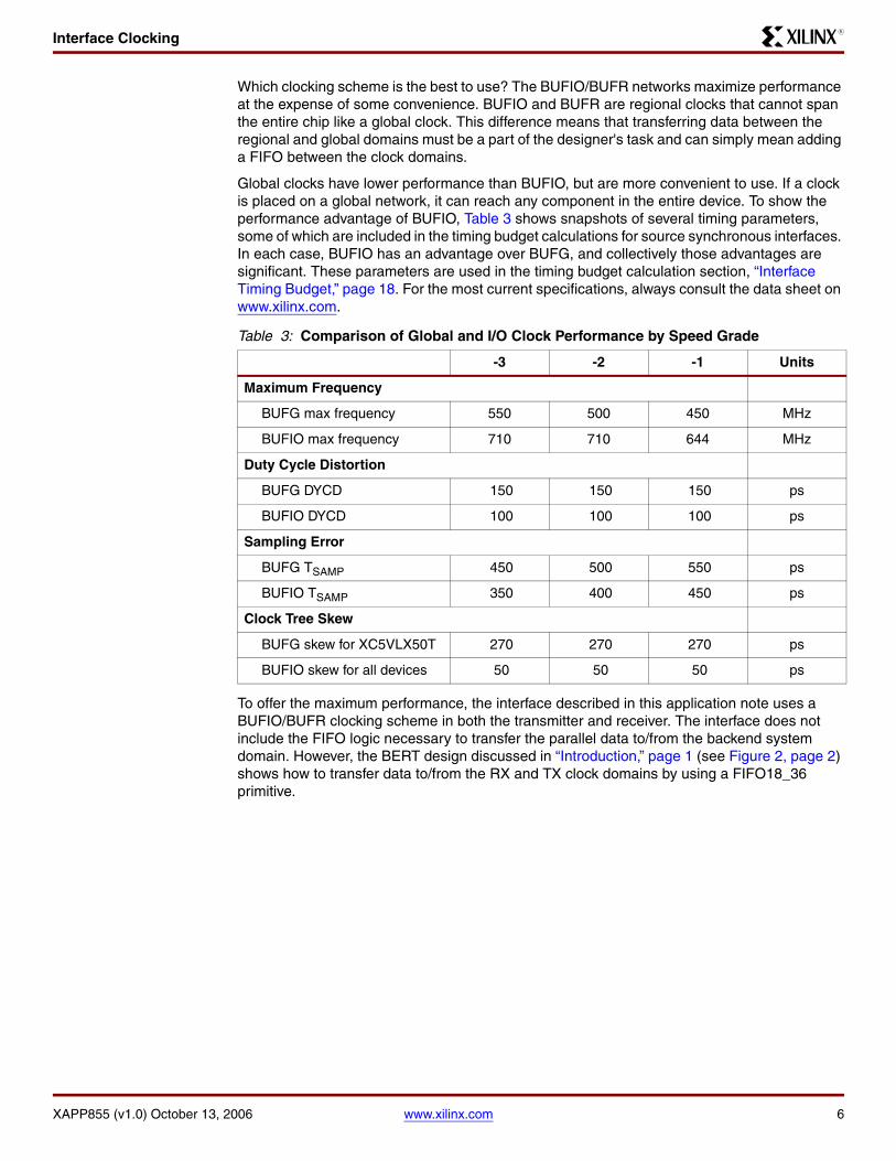
Interface Clocking
XAPP855 (v10) October 13 2006 wwwxilinxcom 6
R
Which clocking scheme is the best to use The BUFIOBUFR networks maximize performance at the expense of some convenience BUFIO and BUFR are regional clocks that cannot span the entire chip like a global clock This difference means that transferring data between the regional and global domains must be a part of the designers task and can simply mean adding a FIFO between the clock domains
Global clocks have lower performance than BUFIO but are more convenient to use If a clock is placed on a global network it can reach any component in the entire device To show the performance advantage of BUFIO Table 3 shows snapshots of several timing parameters some of which are included in the timing budget calculations for source synchronous interfaces In each case BUFIO has an advantage over BUFG and collectively those advantages are significant These parameters are used in the timing budget calculation section ldquoInterface Timing Budgetrdquo page 18 For the most current specifications always consult the data sheet on wwwxilinxcom
To offer the maximum performance the interface described in this application note uses a BUFIOBUFR clocking scheme in both the transmitter and receiver The interface does not include the FIFO logic necessary to transfer the parallel data tofrom the backend system domain However the BERT design discussed in ldquoIntroductionrdquo page 1 (see Figure 2 page 2) shows how to transfer data tofrom the RX and TX clock domains by using a FIFO18_36 primitive
Table 3 Comparison of Global and IO Clock Performance by Speed Grade
-3 -2 -1 Units
Maximum Frequency
BUFG max frequency 550 500 450 MHz
BUFIO max frequency 710 710 644 MHz
Duty Cycle Distortion
BUFG DYCD 150 150 150 ps
BUFIO DYCD 100 100 100 ps
Sampling Error
BUFG TSAMP 450 500 550 ps
BUFIO TSAMP 350 400 450 ps
Clock Tree Skew
BUFG skew for XC5VLX50T 270 270 270 ps
BUFIO skew for all devices 50 50 50 ps
DDR Receiver
XAPP855 (v10) October 13 2006 wwwxilinxcom 7
R
DDR Receiver The DDR receiver consists of three core modules DDR_8TO1_16CHAN_RX BIT_ALIGN_MACHINE and RESOURCE_SHARING_CONTROL The receiver is more complex than the DDR transmitter because it includes a dynamic alignment algorithm implemented in the FPGA fabric The DDR_8TO1_16CHAN_RX module takes 16 channels of data on the serial side optimizes the timing relationship of each channel with the clock performs 18 deserialization and presents 128 bits of data on the parallel side The port list is shown in Table 4
Table 4 DDR_8TO1_16CHAN_RX Module Port Definitions
Port Name IO Definition
DATA_RX_P [150] Input 16 data channels (P)
DATA_RX_N [150] Input 16 data channels (N)
CLOCK_RX_P Input Forwarded clock (P)
CLOCK_RX_N Input Forwarded clock (N)
INC_PAD Input Pulsing this pin causes the IDELAY tap setting of all data channels to increment by 1
DEC_PAD Input Pulsing this pin causes the IDELAY tap setting of all data channels to decrement by 1
DATA_FROM_ISERDES [1270] Output Parallel side data to backend system
RESET Input Reset synchronous to the RX domain
IDLY_RESET Input Reset synchronous to the RX domain that only resets the IDELAY tap settings of all data channels
IDELAYCTRL_RESET Input Reset synchronous to the TX domain that only resets the IDELAYCTRL module
BITSLIP_PAD Input Pulsing this pin causes one bitslip operation on all data channels
CLK200 Input Reference clock to IDELAYCTRL module
TAP_00 TAP_01 TAP_03 TAP_04 TAP_05 TAP_06 TAP_07 TAP_08 TAP_09 TAP_10 TAP_11 TAP_12 TAP_13 TAP_14 TAP_15
Output[50] Each of these 6-bit signals contains the current IDELAY tap value of the sixteen data channels Possible values 0-63
TAP_CLK [50] Output The 6-bit signal containing the current IDELAY tap value of the clock channel Permanently set to zero because the clock channel is not adjusted
TRAINING_DONE Output Flag indicating alignment is complete
RXCLK Output RX Source Sync Clock
RXCLKDIV Output RX Source Sync Clock divided by 4
IDELAY_READY Output Flag indicating IDELAYCTRL is calibrated
DDR Receiver
XAPP855 (v10) October 13 2006 wwwxilinxcom 8
R
Most of the logic used in the receiver is contained within the ISERDES The ISERDES is part of the ChipSync technology and is found in IO of all Virtex-5 devices The ISERDES can be programmed to do any deserialization up to 110 and do single or double data rate reception For deserializations greater than 61 a second ISERDES is needed (taken from the second IO in the LVDS pair) The first ISERDES is called the master and the second ISERDES is called the slave Figure 7 shows a single channel of the RX
Figure 7 MasterSlave ISERDES Pair for a Single Data Channel with 18 Deserialization
MasterISERDES
Serial DataExternal to
FPGA
X855_07_080306
Parallel Datainto FPGA Fabric
SlaveISERDES
SHIFTOUT2SHIFTOUT1
SHIFTIN2SHIFTIN1
Q1
Q2
Q3
Q4
Q5
Q6
Q1
Q2
Q3
Q4
Q5
Q6
Data8
Data7
Data6
Data5
Data4
Data3
Data2
Data1
DDR Receiver
XAPP855 (v10) October 13 2006 wwwxilinxcom 9
R
The receiver interface (Figure 8) consists of 16 masterslave ISERDES pairs Since this interface is source synchronous the clock source comes from the transmitter The clock is buffered in the receiver by a BUFIO component and divided to the parallel clock rate by a BUFR component
Figure 8 Block Diagram of RX Interface
MasterDATA_RX_P[00]
DATA_RX_N[00]
LVDS_25
Slave
IODELAY
CHAN_SELDATA_ALIGNED
DATA_TO_MACHINE
RXCLK(1)
START_ALIGN
Master
LVDS_25
Slave
ISERDES_CH_01 IODELAY
X855_08_082806
DQ
BUFIO
BUFR (divide4)
8 [72]
[10]
[98]
[1510]
[127122]
[121120]
4
8
8 8
3
3
3
DATA_RX_P[01]
DATA_RX_N[01]
Master
LVDS_25
Slave
IODELAY
DATA_RX_P[15]
DATA_RX_N[15]
ISERDES_CH_15
ISERDES_CH_00
RXCLKDIV
INC
ICE
BITSLIP
RXCLKDIV(1)
INC ICEBITSLIP
To CH 15
To CH 01
To CH 00
RX_IDELAYCTRL
Resource SharingControl
Bit AlignMachine
200 MHzSource
LVDS_25
CLOCK_RX_N
CLOCK_RX_P
Notes1 RXCLK and RXCLKDIV drive all ISERDES both master and slave
IODELAY
Fixed to Tap 0
Decoder
DDR Receiver
XAPP855 (v10) October 13 2006 wwwxilinxcom 10
R
Each ISERDES in Figure 8 page 9 contributes 8 bits to the 128-bit parallel data bus Since there is only one instance of BIT_ALIGN_MACHINE in the receiver each data channel must be aligned separately by sharing that resource The 8-bit data buses from each ISERDES are fed into a MUX which selects which of the 16 channels has access to the BIT_ALIGN_MACHINE resource RESOURCE_SHARING_CONTROL controls the MUX to ensure that every channel completes its alignment before the MUX switches to the next channel The START_ALIGN signal tells the BIT_ALIGN_MACHINE that alignment can begin on the current channel because the MUX output is stable The DATA_ALIGNED signal tells the RESOURCE_SHARING_CONTROL module that alignment on the current channel is complete
The order of the parallel data outputs of the ISERDES is the opposite of the parallel data inputs of the OSERDES The least significant OSERDES data inputs are fed into the master while the least-significant ISERDES data outputs come from the slave (Figure 4 page 3 versus Figure 7)
The IDELAYCTRL module in Figure 8 is shown as having no connection to the rest of the receiver Actually IDELAYCTRL is required to calibrate the IODELAY blocks in the path of each data channel A single IDELAYCTRL block is sufficient to calibrate all 16 data channels since all channels are in the same bank
The BIT_ALIGN_MACHINE generates three control signals that adjust the timing of the appropriate ISERDES INC and ICE cause the IODELAY to increment or decrement the delay in the datapath by a fixed amount of ~75 ps (if a 200 MHz reference clock is used) BITSLIP causes each ISERDES to rotate the order of the parallel output data bits facilitating the process of word alignment These three control signals are directed to the appropriate ISERDES by the decoder shown in Figure 8 Although not shown in the figure the decoder is also controlled by the RESOURCE_SHARING_CONTROL module
Table 5 shows the device utilization statistics for the RX interface implemented in a Virtex-5 device These figures exclude the counters used to track the IODELAY settings on all data channels in most instances those counters can be removed after the interface is integrated and verified in a specific environment The majority of the LUTs utilized are consumed by the BIT_ALIGN_MACHINE which is the core of the receiver alignment algorithm As in the TX interface the RX interface consumes one BUFIO and one BUFR for clocking The clocking could also be accomplished using BUFGs and a DCM as described in ldquoInterface Clockingrdquo page 5 but the performanceconvenience trade off would need to be considered
Table 5 DDR RX Interface Utilization Statistics
Component Quantity Usage Description
Slice Flip-Flop 131 Multiple uses
Slice 105 Multiple uses
LUT 263 Multiple uses
IOB 34 17 LVDS input pairs (16 data 1 clock)
ISERDES 32 Master and slave ISERDES for every LVDS data pair
BUFIO 1 RXCLK
BUFR 1 RXCLKDIV
Receiver Interface Dynamic Timing
XAPP855 (v10) October 13 2006 wwwxilinxcom 11
R
Receiver Interface Dynamic Timing
The timing of the receiver interface is broken into two parts
bull The suboptimal timing inherent in the data and clock paths
bull The optimal timing created by the receiver when adjusting dynamic delays on each of the 16 data channels
Inherent Timing
An inventory of all propagation delays in the clock and datapaths must be taken to derive the inherent setuphold times The clock and datapaths for a single channel of this interface are shown in Figure 9 The ISE Timing Analyzer breaks down the paths into the timing parameters shown All components in the path have both a minimum and maximum value to account for process variations
Figure 10 page 12 shows the timing analyzer settings used to generate the information in this report Each of the timing parameters is described in Table 6 page 12 and Table 7 The minimum and maximum values of the individual timing parameters for the clock and datapaths are shown in Table 8 and Table 9 page 13
Note All raw timing numbers referenced in this document are subject to minor changes in subsequent revisions of the ISE tools
Figure 9 Timing Components of RX Data and Clock Paths
ISERDESFFsIODELAY
VariableInit to 0
DI O
CLK
IODELAYIBUFDS
IBUFDS
+
ndash
+
ndash Fixed toTap 0
I O
X855_09_082806
DataPath
ClockPath
TIOPI TIODDO_IDATAINTNET1 TNET2
TIOPI TIODDO_IDATAIN TISDCK_DDLY
TBUFIOCKO_O
BUFIO
Receiver Interface Dynamic Timing
XAPP855 (v10) October 13 2006 wwwxilinxcom 12
R
Figure 10 ISE Timing Analyzer Properties Used in this Document
Table 6 Datapath Timing Definitions
Timing Parameter Description
TIOPI Delay from the IOB pad through the LVDS input buffer to the I pin of the IOB pad
TIODDO_IDATAIN Delay from the I pin of IOB pad to the D input of the ISERDES
TISDCK_DDLY Delay from the D input of the ISERDES to the sampling registers in the ISERDES (setup and hold times of ISERDES)
Table 7 Clock Path Timing Definitions
Timing Parameter Description
TIOPI Delay from the IOB pad through the LVDS input buffer to the I pin of the IOB pad
TIODDO_IDATAIN Delay from I pin of IOB pad to the O output of the IODELAY block
TNET1 Delay from the O output of the IODELAY block to the I pin of BUFIO
TBUFIOCKO_O Clock to out delay of BUFIO
TNET2 Clock distribution delay from BUFIO output to the clock input of data ISERDES
Table 8 Datapath Delay Inventory for a -1 Speed Grade XC5VLX50T Device
Timing Parameter Maximum Datapath Delay Minimum Datapath Delay
TIOPI 1083 ns 0763 ns
TIODDO_IDATAIN 0671 ns 0671 ns
TISDCK_DDLY 0064 ns ndash0038 ns
TOTAL 1818 ns 1396 ns
XAPP855_10_071306
Receiver Interface Dynamic Timing
XAPP855 (v10) October 13 2006 wwwxilinxcom 13
R
According to the inherent timing prediction the data is going to arrive before the clock by an amount determined by Equation 1 and Equation 2 Equation 1 calculates that data arrives before the clock by at least 1076 ns in a -1 device Equation 2 calculates that data arrives before the clock by at most 2213 ns Equation 3 shows a timing window that covers all -1 devices under all conditions This timing window describes the inherent timing of the data and clock paths Assuming skew-matched PCB traces for all sixteen channels then it can be assumed that all 16 channels in the receiver have roughly the same timing window
Equation 1
Equation 2
Equation 3
Figure 11 shows the timing windows for all speed grades of an XC5VLX50T device as well as a hardware measurement of the inherent timing relationship (to validate the calculations) The hardware measurement shows the DDR interface data arriving 1425 ns before the clock which by inspection places the device in all three speed grade ranges (the device used for the hardware measurement is a -2 device)
Table 9 Clock Path Delay Inventory for a -1 Speed Grade XC5VLX50T Device
Timing Parameter Maximum Clock Path Delay Minimum Clock Path Delay
TIOPI 1150 ns 0820 ns
TIODDO_IDATAIN 0671 ns 0671 ns
TNET1 0254 ns 0190 ns
TBUFIOCKO_O 1130 ns 0894 ns
TNET2 0404 ns 0319 ns
TOTAL 3609 ns 2894 ns
Setup Time Max Data Delay Min Clock Delay 1818 2894ndash 1076 nsndash==ndash=
Hold Time Max Clock Delay Min Data Delay 3609 1396ndash 2213 ns==ndash=
Timing Window 2213 1076ndash 1137 ns==
Figure 11 Timing Windows Show Uncertainty in ClockData Relationship as Calculated by Timing Analyzer
400 Mbs Data (T = 25 ns)
1425 ns Hardware MeasurementData Arrives
x855_11_091806
-11076ns 2213 ns
-21043 ns 2039 ns
-30989 ns 1878 ns
Receiver Interface Dynamic Timing
XAPP855 (v10) October 13 2006 wwwxilinxcom 14
R
Dynamic Timing and BIT_ALIGN_MACHINE
In ldquoInherent Timingrdquo page 11 the inherent timing of the interface was calculated for all speed grades and validated with a hardware measurement In that case the inherent timing was sufficient because the data rate is only 400 Mbs (Figure 11 page 13) What happens when the data rate is increased such that the hold edge of the data window begins to shrink (Figure 12)
At 600 Mbs the inherent timing relationship is no longer adequate to meet timing because there are cases when the sampling clock edge is in the middle of the data transition As the data rates increase to 800 and 1000 Mbs the clock actually captures the data arriving one bit time later For designs that are sensitive to word alignment this is unacceptable
The solution to the suboptimal inherent timing is dynamic timing The BIT_ALIGN_MACHINE module in the receiver performs two functions of dynamic timing
bull Bit Alignment Position the sampling edge of the clock at the center of the data eye by adding delay to the datapaths
bull Word Alignment Ensure that the parallel data bits are in the correct order at the output of the ISERDES by using the bitslip function in the ISERDES
The steps of the bit-alignment procedure are shown in Figure 13 page 15 Each step of the algorithm can either add or subtract delay from the datapath All 16 channels are taken through this procedure independently This procedure measures one full data eye (in terms of 75 ps delay taps) and then returns to the center of the data eye Steps 1 and 2 are dedicated to moving through the partial eye of the initial timing while steps 3 and 4 are dedicated to measuring a full eye Step 5 is dedicated to positioning the clock edge at the center of the data eye
Figure 12 Inherent Timing Windows Shown in Relation to Multiple Data Rates
400 Mbs Data (T = 25 ns)
600 Mbs Data (T = 167 ns)
800 Mbs Data (T = 127 ns)
1000 Mbs Data (T = 10 ns)
-11076ns 2213 ns
-21043 ns 2039 ns
-30989 ns
1425 ns
1878 ns
Hardware MeasurementData Arrives
x855_12_091806
Receiver Interface Dynamic Timing
XAPP855 (v10) October 13 2006 wwwxilinxcom 15
R
Jitter is represented in Figure 13 as multiple transition lines Accounting for jitter is a crucial part of the algorithm In step 2 the first data transition is found If there is no jitter then the eye measurement can begin instantly after finding the transition However when jitter is considered the algorithm must find the first transition move through the transition and then begin looking for the second transition If the algorithm does not move through the first transition intelligently it runs the risk of falsely detecting the second transition
Once bit alignment is complete the order of the data bits can be adjusted to achieve word alignment The bit-alignment procedure ensures that data is being sampled correctly but the order of the data can be a few bits off from where the receiver expects it to be To correct this the bitslip feature of the ISERDES is used to slip bit times until the proper alignment is found For this feature to be useful a training pattern must be generated by the transmitter (as discussed in ldquoDDR Transmitterrdquo page 3) that the receiver can use to determine the proper word alignment In this reference design the training pattern is 00101100 (0x2C) This pattern is mostly arbitrary as many other patterns work just as well This pattern was chosen because a training pattern should behave electrically as much like real data as possible such that the center of the training eye is the center of the data eye Since real data contains strings of consecutive ones and zeros it is best for the training pattern to do the same For that reason a 0x2C pattern is better than an 0xAA pattern because it contains run lengths of 1 2 3 and 4 bit times
Table 10 page 16 shows the word-alignment process in the case where bit alignment completes with the data outputs set to 0x58 Since 0x58 is not the training pattern the receiver is looking for bitslip is asserted until 0x2C is found This reference design uses a 18 deserialization so there are only eight possible configurations of the parallel data outputs If bitslip is asserted infinitely the same eight configurations will repeat Bitslip in DDR mode is somewhat irregular because it does not simply rotate by one bit on every bitslip cycle This effect is inconsequential to the word-alignment procedure (see the Virtex-5 User Guide for more details)
Figure 13 Dynamic Bit-Alignment Procedure in BIT_ALIGN_MACHINE
Data 0
Data Arrives Before Clock
Data 1
x855_13_091806
Data 0 Data 1
Data 0 Data 1
Data 0 Data 1
Data 0 Data 1
Sampling Clock (Fixed Delay)
Return to Center of Eye
End Measuring Eye
Begin Measuring Eye
Find 1st Transition
Initial Timing1
2
3
4
5
Receiver Interface Dynamic Timing
XAPP855 (v10) October 13 2006 wwwxilinxcom 16
R
The FSM in the BIT_ALIGN_MACHINE module used to implement both bit and word alignment is shown in Figure 14 page 17 The FSM is divided into five sections loosely described as finding the first transition getting through the first transition finding the second transition returning to the center of the eye and word alignment
To get through the first transition effectively for all possible types of jitter two methods are used The first method pertains to random jitter If there is a lot of random jitter at the sampling point then the samples generated are not stable The algorithm detects this instability by comparing current samples to older samples and therefore knows where the transition begins and ends But what if the jitter is extremely deterministic The transition then has discreet crossing points such that within the transition there is very stable but incorrect data In this case the algorithm does not sense any instability and falsely concludes that the sampling point is not in the transition To address this case apart from evaluating stability the algorithm also evaluates the correctness of the data content by using the bitslip feature in the middle of the transition For example if the algorithm determines that the sampled data is stable it then asserts bitslip to look for the correct data If 0x2c is found within eight assertions of bitslip then the sampling point is not in the transition But if 0x2c is not found then the algorithm increments the data delay and repeats the transition test again
Table 10 Word Alignment in the DDR Receiver
Bitslip Cycle Data Value (Hex) Data Value (Bin) Description of Bitslip operation
1 58 0101 1000 ndash
2 0B 0000 1011 Rotate 3 bits to right
3 16 0001 0110 Rotate 1 bit to left
4 C2 1100 0010 Rotate 3 bits to right
5 85 1000 0101 Rotate 1 bit to left
6 B0 1011 0000 Rotate 3 bits to right
7 61 0110 0001 Rotate 1 bit to left
8 2C 0010 1100 Rotate 3 bits to right
Receiver Interface Dynamic Timing
XAPP855 (v10) October 13 2006 wwwxilinxcom 17
R
Figure 14 FSM in the BIT_ALIGN_MACHINE Module
TRANSITION_CHECK (01000)
First TransitionNot Detected
First TransitionNot Detected
First TransitionDetected
First TransitionDetected
Past the FirstTransition
Second TransitionNot Detected
Second TransitionDetected
Decrement DelayAgain
Bit AlignmentComplete
Still Samplingin Transition
INC_ONCE (01111)
SEARCH_PAT (01101)
IDLE (01100)
IDLE (10000)
RECHECK_TRANS (00010)
ONE_BITSLIP (00110)
INC_ONCE (01011)
WAIT_8_CYCLES (00100)
COUNT_1 (01110)
INC_ONCE (01001)
WAIT_8_CYCLES (00011)
IDLE (10010)
TRAINING_DONE (00111)
FIRST_SAMPLE (00001)
RESET (00000)
DEC_TO_HALF (01010)
WORD_ALIGN (00101)
X855_14_082806
Routine to Avoid False Detection of Second Transition
=CHECK_PATTERN
Receiver Interface Dynamic Timing
XAPP855 (v10) October 13 2006 wwwxilinxcom 18
R
Interface Timing Budget
In addition to sampling the data as closely as possible to the center of the data eye the actual size of the data eye is important By accurately predicting the size of the data eye in the receiver the overall performance ceiling of the interface can be inferred The ideal data eye width is the period of the data rate (for example TBit_Period = 100 ns for 1000 Mbs) Both the transmitter and receiver circuits have sources of error that subtract from the ideal data eye The equation for the eye width at the output of the transmitter is shown in Equation 4 TJITTER is the peak-to-peak jitter of the clock source driving the transmitter data bus and forwarded clock TDCD is the maximum duty cycle distortion of the clock tree driving the data bus and forwarded clock Skew is not considered in the transmitter or receiver because the receiver calibrates out skew between channels by performing alignment on each channel individually
Equation 4
Equation 5 calculates the width of the data eye at the receiver flip-flops Ideally the eye width at the receiver is the same as the eye width at the output of the transmitter but there are sources of error in the transmission medium and receiver circuitry Duty cycle distortion must be considered again on the receiver clock tree TSAMP_BUFIO is the receiver sampling error due to drift caused by voltage and temperature variations TIDELAYPAT_JIT is the amount of pattern dependent jitter that is accumulated in each tap of the IDELAY chain For a clock pattern TIDELAYPAT_JIT is 0 pstap peak to peak For a data pattern with long and short run lengths of zeroes and ones (simulated by PRBS23) TIDELAYPAT_JIT is a finite value that must be considered in the timing budget
Equation 5
TBOARD_JITTER includes jitter induced by receiver input capacitance and the parasitics of the physical data path on the PCB TBOARD_JITTER must be determined by simulation as it varies as a function of frequency and for receivers of different types and vendors On the ML550 with a -2 speed-grade Virtex-5 device the TBOARD_JITTER is measured at roughly 200 ps at 900 Mbs (assuming data content equivalent to PRBS23) TQUANTIZATION_ERR or quantization error is caused by the granularity of the IDELAY tap chain Working with 75 ps increments it is not possible to utilize the entire data eye since inevitably some valid eye width is lost between two taps The value for this loss is 75 ps As long as the receiver eye width calculated using Equation 5 is greater than or equal to 0 the interface operates correctly over process voltage and temperature
For example Equation 6 and Equation 7 show the timing budget calculation for the DDR interface running at 900 Mbs in a -2 speed grade device on an ML550 evaluation board Refer to the data sheet for the most current values The TX interface is looped back to the RX interface on the same Virtex-5 FPGA as shown in Equation 2
Equation 6
Equation 7
Changes in voltage and temperature cause the data channels of the interface to drift relative to the clock If the DDR interface were to transfer user data for a long period of time over all specified conditions of temperature and voltage Equation 7 states that there would be at least 107 ps (one or two IDELAY taps) of data window remaining valid during all fluctuations of temperature and voltage Compare this calculation to the measurements in Table 12 page 21 Case 900 Mbs There are four taps that are error free under all conditions In ldquoAppendixrdquo there are three -2 devices tested at 900 Mbs and each has 4 4 and 3 taps respectively that are error free under all conditions
DATA_EYE_WIDTH_TX TBIT_PERIOD TJITTERndash TDCD_BUFIOndash=
DATA_EYE_WIDTH_RX DATA_EYE_WIDTH_TX
TBOARD_JITTER
ndash
TSAMP_BUFIOndash TDCD_BUFIOndash
TIDELAYPAT_JIT IDELAY taps in datapathtimes[ ]ndash
TQUANTIZATION_ERRndash
=
DATA_EYE_WIDTH_TX 1111 ps 25 psndash 100 psndash 986 ps= =
DATA_EYE_WIDTH_RX986 ps 200 psndash 400 psndash 100 psndash 8 ps 13 tapstimes[ ] 75 ps 107 ps=ndashndash
=
Interface Characterization
XAPP855 (v10) October 13 2006 wwwxilinxcom 19
R
At a given temperature and voltage setting the data valid window is much larger because there is no drift when temperature and voltage are constant The size of the data valid window under constant conditions is 107 ps + TSAMP_BUFIO which in this case is at least 507 ps (six or seven IDELAY taps) Compare this calculation to the measurements of any single condition in Table 12 Case 900 Mbs In the worst case (ndash5 supply) there are 7 taps that are error free
Equation 8 and Equation 9 show the same timing budget calculation for the DDR interface running at 10 Gbs in a -2 speed grade device on an ML550 Evaluation Board
Equation 8
Equation 9
Equation 9 predicts that no data window remains valid during all specified fluctuations of temperature and voltage (compare to Table 12 Case 1000 Mbs) In ldquoAppendixrdquo there are three -2 devices tested at 1000 Mbs and each has 1 3 and 1 taps respectively that are error free under all conditions This data rate and device combination are very marginal cases
To operate at 10 Gbs the DDR interface requires additional circuitry to track out voltage-temperature variations in real-time (see XAPP860 16-channel DDR LVDS Interface with Real-time Window Monitoring for a DDR Interface with real-time window monitoring) If the voltage-temperature variations are removed from the picture the predicted data valid window is ndash120 ps + TSAMP_BUFIO which in this case is at least 280 ps (3 or 4 taps) Compare this calculation to the measurements of any single condition in Table 18 page 34 There are at least four error-free taps in all conditions
Interface Characterization
By following the procedure illustrated in Figure 13 page 15 the bit-alignment algorithm should never insert more than approximately 15 bit times of delay on the data channels The fewest number of delay taps should be used in the datapath because they produce a finite amount of degradation (TIDELAYPAT_JIT) The worst-case initial timing for the algorithm occurs when the clock samples just before the data transitions as in the 600 Mbs case in Figure 12 page 14 The algorithm must move all the way through the first eye to find the first transition (1 bit time) and then move halfway into the next eye to center the sampling point (05 bit time) This process produces a worst-case total delay insertion of 15 bit times
The actual performance of the bit-alignment algorithm is characterized as a function of data rate in Figure 15 page 20 For all data rates the expectation is that the tap settings of all 16 channels in the DDR receiver do not exceed approximately 15 bit times of delay Both the maximum and minimum tap setting of all 16 channels is recorded for each data rate This graph only shows the data for a single device Comparing the 15 bit time mask to the actual settings it is clear that the algorithm remains within the 15 bit time limit At 13 Gbs the tap setting actually exceeds the mask by one tap (a negligible violation)
DATA_EYE_WIDTH_TX 1000 ps 25 psndash 100 psndash 875 ps= =
DATA_EYE_WIDTH_RX 875 ps 300 psndash400 ps 100 psndash
ndash8 ps 15 tapstimes[ ] 75 ps 120 psndash=ndashndash
=
Interface Characterization
XAPP855 (v10) October 13 2006 wwwxilinxcom 20
R
The maximum and minimum tap settings in Figure 15 generally stay within 3 to 4 taps of each other except in the case of 640 Mbs and 1300 Mbs data rates These data rates are seams in the inherent timing At data rates below 640 Mbs the tap settings are in the range of 30 taps and at data rates above 640 Mbs the tap settings are in the range of 12 taps Referring back to Figure 12 page 14 it is clear why this seam occurs As the data rate increases past 600 Mbs the initial sampling point of the inherent timing moves into a different data eye creating a different starting point for the algorithm At 640 Mbs some of the 16 channels start in one eye while other channels start in the other eye Fortunately this is not an issue because the single bit time of difference between the channels is resolved using bitslip
Referring back to Figure 8 page 9 the clock channel goes through an IDELAY block with a default value of 0 Once the data rate is chosen for a given design this initial IDELAY value can be changed to a non-zero value to achieve more favorable inherent timing For example a design running at 620 Mbs can use 30 IDELAY taps on the delay channels each contributing a certain amount of jitter to the timing budget calculation By setting the initial clock delay to 5 taps the inherent timing moves across the seam shown in the 600 Mbs range of Figure 15 causing the data channels to only use about 12 IDELAY taps Only spectrally rich data patterns accumulate jitter in the IDELAY tap chain so the clock IDELAY can be set to any value without diminishing the timing budget This optimization is entirely optional and can be done once the design is running in hardware
The DDR receiver is designed to remove skew between channels by aligning each channel individually The ML550 board on which this reference design is characterized is designed to have minimal skew between channels However there is clearly a finite amount of skew between channels due to clock skew in the TX and RX BUFIO networks package skew and trace length tolerance on the ML550 board Table 11 page 21 shows how the bit-alignment algorithm sets the delay for each channel differently to compensate for skew between channels The table captures the range of settings among the 16 channels at specific data rates for a -2 device If there were additional skew among the 16 channels then the tap setting range would be larger to compensate for it The algorithm is designed such that skew between channels should not diminish the performance of the interface The range of tap settings differs for different devices and speed grades but the magnitude should be approximately the same
Figure 15 Bit-Alignment Algorithm Performance
60
50
40
30
20
10
0200 400 600 800 1000 1200 1400 1600
Data Rate (Mbs)
Del
ay T
ap U
tiliz
atio
n HW Measurement (Min)HW Measurement (Max)15 Bit Time Mask
X855_15_072406
Interface Characterization
XAPP855 (v10) October 13 2006 wwwxilinxcom 21
R
Since the receiver alignment logic only runs once immediately after reset the resulting dynamic timing must be adequate to ensure error-free operation over the specified voltage and temperature variations that can occur over time The data-valid window at the receiver input must be wide enough to withstand these variations (receiver drift) Table 12 page 21 shows the data-valid window at the ISERDES registers in the DDR receiver The eyes shown are collective eyes of all 16 channels The BERT testbench configuration loops back the DDR transmitter to the DDR receiver Using pattern generators and error detectors programmed to send and receive a pseudorandom bit sequence (PRBS23) the width of the data-valid window is evaluated using pseudorandom data that closely resembles real user data
Table 11 Tap Setting Range For Various Data Rates Measured on a -2 Device
Data Rate (Mbs) Tap Setting Range Compensated Skew
500 31ndash34 4 taps
600 28ndash30 3 taps
700 10ndash12 3 taps
800 11ndash13 3 taps
900 11ndash13 3 taps
1000 13ndash15 3 taps
1100 13ndash15 3 taps
1200 14ndash15 2 taps
Table 12 Measurement of Receiver Drift under Extreme Conditions for Multiple Data Rates
ConditionIODELAY Taps (1)
ndash8 ndash7 ndash6 ndash5 ndash4 ndash3 ndash2 ndash1 0 +1 +2 +3 +4 +5 +6 +7 +8
Case 800 Mbs
25degC Nom Supplies F F F P P P P P C P P P P P F F F
0degC Nom Supplies F F F P P P P P P P P P P P F F F
85degC Nom Supplies F F F P P P P P P P P P P P F F F
25degC +5 Supplies F P P P P P P P P P P P F F F F F
0degC +5 Supplies F P P P P P P P P P P P F F F F F
85degC +5 Supplies F P P P P P P P P P P P F F F F F
25degC ndash5 Supplies F F F F F F P P P P P P P P P F F
0degC ndash5 Supplies F F F F F F P P P P P P P P P P F
85degC ndash5 Supplies F F F F F P P P P P P P P P P F F
CONCLUSION Error free under all conditions when calibrated under nominal conditions to position C
Interface Characterization
XAPP855 (v10) October 13 2006 wwwxilinxcom 22
R
Case 900 Mbs
25degC Nom Supplies F F F F P P P P C P P P P F F F F
0degC Nom Supplies F F F F P P P P P P P P P F F F F
85degC Nom Supplies F F F F P P P P P P P P F F F F F
25degC +5 Supplies F F P P P P P P P P P F F F F F F
0degC +5 Supplies F F P P P P P P P P P F F F F F F
85degC +5 Supplies F F P P P P P P P P P F F F F F F
25degC ndash5 Supplies F F F F F F F P P P P P P P P F F
0degC ndash5 Supplies F F F F F F F P P P P P P P P F F
85degC ndash5 Supplies F F F F F F F P P P P P P P F F F
CONCLUSION Error free under all conditions when calibrated under nominal conditions to position C
Case 1000 Mbs
25degC Nom Supplies F F F F F P P P C P P P F F F F F
0degC Nom Supplies F F F F F P P P P P P P F F F F F
85degC Nom Supplies F F F F F P P P P P P P F F F F F
25degC +5 Supplies F F F P P P P P P P F F F F F F F
0degC +5 Supplies F F F P P P P P P P F F F F F F F
85degC +5 Supplies F F F P P P P P P P P F F F F F F
25degC ndash5 Supplies F F F F F F F F P P P P P P F F F
0degC ndash5 Supplies F F F F F F F F P P P P P P F F F
85degC ndash5 Supplies F F F F F F F F P P P P P P F F F
CONCLUSION Error free under all conditions when calibrated under nominal conditions to position C
Case 1100 Mbs
25degC Nom Supplies F F F F F P P P C P F F F F F F F
0degC Nom Supplies F F F F F P P P P P F F F F F F F
85degC Nom Supplies F F F F F P P P P P F F F F F F F
25degC +5 Supplies F F F P P P P P P F F F F F F F F
0degC +5 Supplies F F F P P P P P P F F F F F F F F
85degC +5 Supplies F F F P P P P P P F F F F F F F F
25degC ndash5 Supplies F F F F F F F F P P P P F F F F F
0degC ndash5 Supplies F F F F F F F F P P P P F F F F F
85degC ndash5 Supplies F F F F F F F F P P P P F F F F F
CONCLUSION Error free under all conditions when calibrated under nominal conditions to position C
Table 12 Measurement of Receiver Drift under Extreme Conditions for Multiple Data Rates (Continued)
ConditionIODELAY Taps (1)
ndash8 ndash7 ndash6 ndash5 ndash4 ndash3 ndash2 ndash1 0 +1 +2 +3 +4 +5 +6 +7 +8
Interface Characterization
XAPP855 (v10) October 13 2006 wwwxilinxcom 23
R
In all test cases shown in Table 12 page 21 the bit-align machine accurately places the sampling point in the center of the data eye (indicated by the C in each test case) In the 1100 Mbs case the bit-align machine places the sampling point slightly off center This slight inaccuracy occurs when the center of a real data pattern diverges from the center of the training pattern The electrical behavior of different data patterns is discussed below
After the dynamic timing is established for a given test case under nominal conditions the device is subjected to extremes of temperature and voltage to stress the receiver timing At data rates of 1100 Mbs and below the dynamic timing established after reset under nominal conditions is sufficient to meet timing over all specified extreme conditions (the column with the C passes traffic error free under all conditions) At a data rate of 1200 Mbs the design operates correctly under nominal conditions but the data-valid window is not large enough to withstand the voltage variations For this particular transmission medium the 1200 Mbs case requires a real-time adjustment circuit that could track the center of the eye
The full datapath of the testbench consists of
TX rarr 5 FR-4 rarr SAMTEC QSE Conn rarr 12 Ribbon Cable rarr SAMTEC QSE Conn rarr 5 FR-4 rarr RX
For shorter transmission media higher performance can be achieved in accordance with the section ldquoInterface Timing Budgetrdquo page 18 Interface performance is not solely a question of the LVDS driver performance specification but rather a question of adequate timing margin to withstand production and environmental variations From Table 12 the total amount of variation experienced over temperature and voltage is roughly 375 ps (5 taps at 75 ps per tap) This number should be comparable to the specification for receiver sampling error (TSAMP_BUFIO) shown in the Virtex-5 Data Sheet
Case 1200 Mbs
25degC Nom Supplies F F F F F F P P C P F F F F F F F
0degC Nom Supplies F F F F F F P P P P F F F F F F F
85degC Nom Supplies F F F F F F P P P F F F F F F F F
25degC +5 Supplies F F F F P P P P F F F F F F F F F
0degC +5 Supplies F F F P P P P P F F F F F F F F F
85degC +5 Supplies F F F F P P P P F F F F F F F F F
25degC ndash5 Supplies F F F F F F F F F P P P F F F F F
0degC ndash5 Supplies F F F F F F F F F P P P F F F F F
85degC ndash5 Supplies F F F F F F F F F P P F F F F F F
CONCLUSION Errors caused by plusmn5 variations in supply voltages
Notes 1 Where 0 is the reference tap determined by the bit-align machine under nominal conditions at 25degC2 P = Error-free transmission F = Error in transmission C = IODELAY tap position selected by bit-align machine under nominal conditions at 25degC3 Device under test is -2 speed grade
Table 12 Measurement of Receiver Drift under Extreme Conditions for Multiple Data Rates (Continued)
ConditionIODELAY Taps (1)
ndash8 ndash7 ndash6 ndash5 ndash4 ndash3 ndash2 ndash1 0 +1 +2 +3 +4 +5 +6 +7 +8
Interface Characterization
XAPP855 (v10) October 13 2006 wwwxilinxcom 24
R
Pattern Dependence of Receiver Performance
Different types of data patterns have different electrical signatures (rise and fall times jitter eye symmetry etc) A pattern with very narrow spectral content (such as a clock pattern) moves very favorably through the link because the receiver frequency response has little effect on the signal integrity However a pattern with wide spectral content (such as real data and pseudorandom patterns) stresses the links frequency response If the frequency response is not flat across the entire spectrum of the data content then the signal integrity is degraded as a result The amount of degradation measured is shown in Table 13 page 25 The DDR transmitter is looped back to the DDR receiver and different patterns are programmed to traverse the link Performance is assessed by evaluating the integrity of those patterns in the receiver
PRBS7 is a pseudorandom data pattern with a maximum run length of seven consecutive zeroes or ones PRBS15 is defined as having a maximum run length of fifteen consecutive zeroes or ones These limitations on run lengths limit the spectral content of the pattern A PRBS15 pattern has greater spectral content than a PRBS7 pattern and therefore is a more strenuous test for the link PRBS29 is the most strenuous test in Table 13 A clock pattern is effectively a PRBS1
As predicted Table 13 shows that there is more degradation for data patterns with more spectral content At 1000 Mbs and below the data eye closure is symmetrical Symmetrical eye closure is desired because it does not change the center of the eye as determined by the bit-alignment algorithm Above 1000 Mbs the eye closure becomes more asymmetrical causing the center of the data eye to diverge from the calibrated center (by only 1 tap)
In every data rate shown in Table 13 all significant pattern-dependent degradation is caused between PRBS1 (clock pat) and PRBS15 Between PRBS15 and PRBS29 there is no additional degradation recorded in any of the measurements
Interface Characterization
XAPP855 (v10) October 13 2006 wwwxilinxcom 25
R
Table 13 Link Performance for Various Types of Data Measured on a -2 Device
PatternIODELAY Taps (1)
ndash8 ndash7 ndash6 ndash5 ndash4 ndash3 ndash2 ndash1 0 +1 +2 +3 +4 +5 +6 +7 +8 +9
Case 600 Mbs
Clock Pat (0101) P P P P P P P P C P P P P P P P P P
Training Pat (0x2C) P P P P P P P P C P P P P P P P P F
PRBS7 P P P P P P P P C P P P P P P P P F
PRBS15 F P P P P P P P C P P P P P P P F F
PRBS23 F P P P P P P P C P P P P P P P F F
PRBS29 F P P P P P P P C P P P P P P P F F
Case 800 Mbs
Clock Pat (0101) F F P P P P P P C P P P P P P F F F
Training Pat (0x2C) F F P P P P P P C P P P P P P F F F
PRBS7 F F P P P P P P C P P P P P F F F F
PRBS15 F F F P P P P P C P P P P P F F F F
PRBS23 F F F P P P P P C P P P P P F F F F
PRBS29 F F F P P P P P C P P P P P F F F F
Case 1000 Mbs
Clock Pat (0101) F F F P P P P P C P P P P P F F F F
Training Pat (0x2C) F F F P P P P P C P P P P F F F F F
PRBS7 F F F F P P P P C P P P F F F F F F
PRBS15 F F F F F P P P C P P P F F F F F F
PRBS23 F F F F F P P P C P P P F F F F F F
PRBS29 F F F F F P P P C P P P F F F F F F
Case 1200 Mbs
Clock Pat (0101) F F F F P P P P C P P P P F F F F F
Training Pat (0x2C) F F F F P P P P C P P P F F F F F F
PRBS7 F F F F F P P P C P F F F F F F F F
PRBS15 F F F F F F P P C F F F F F F F F F
PRBS23 F F F F F F P P C F F F F F F F F F
PRBS29 F F F F F F P P C F F F F F F F F F
Case 1400 Mbs
Clock Pat (0101) F F F F F F P P C P P P F F F F F F
Training Pat (0x2C) F F F F F P P P C P P F F F F F F F
PRBS7 F F F F F F F P C P F F F F F F F F
PRBS15 F F F F F F F P C F F F F F F F F F
PRBS23 F F F F F F F P C F F F F F F F F F
PRBS29 F F F F F F F P C F F F F F F F F F
Notes 1 Where 0 is the reference tap determined by the bit-align machine under nominal conditions at 25degC2 P = Error-free transmission F = Error in transmission C = IODELAY tap position selected by bit-align machine under nominal conditions at 25degC
Resetting the Interface
XAPP855 (v10) October 13 2006 wwwxilinxcom 26
R
Resetting the Interface
Several dependencies determine the order in which circuits should be reset in the interface The receiver cannot begin the alignment algorithm if the transmitter is not sending the training pattern The transmitter must be reset before the receiver and time must be allowed for the training pattern to propagate across the link before the receiver comes out of reset The receiver also cannot begin the alignment algorithm until IDELAYCTRL has recovered from reset which could takes hundreds of cycles The recommended reset timing for the interface is shown in Figure 16 This reset timing is implemented in the BERT testbench for this interface
The TX reset (RST_TX) is used to reset all TX circuitry and also IDELAYCTRL The IDELAYCTRL reset is asynchronous so driving it with RST_TX is acceptable The minimum pulse width of IDELAYCTRL reset is 50 ns (TIDELAYCTRL_RPW) For that reason resets are held High for 16 clock cycles The RX reset (RST_RX) is used to reset all RX circuitry and is asserted when the IDELAYCTRL READY flag goes High indicating that the IODELAY blocks are calibrated
The timing of the READY flag in Figure 16 is a potential hazard Most likely it is High during a TX reset because it takes many cycles for IDELAYCTRL to deassert the READY flag It is easy to make the mistake of resetting the receiver too early To avoid this hazard the RX reset should be asserted only after seeing a deassertion and reassertion of the READY flag
Conclusion Based on the design and characterization described in this document the 16-Channel DDR reference design operates to the performance targets in Table 14 under all conditions of process voltage and temperature However to meet these targets over voltage and temperature the timing budget must be guaranteed according to the analysis in ldquoInterface Timing Budgetrdquo See ldquoAppendixrdquo page 27 for further justification of the maximum performance recommendations in Table 14
Figure 16 Recommended Interface Reset Timing
RST_TX
IDELAYCTRLREADY
RST_RX
16 Cycles X855_16_072406
Table 14 Performance of 16-Channel DDR Interface
Speed Grade Maximum Performance
-1 800 Mbs
-2 900 Mbs
-3 10 Gbs(1)
Notes 1 To achieve higher performance (up to 125 Gbs) see 16-channel DDR LVDS Interface with Realtime
Window Monitoring for an example of a DDR interface with real-time window monitoring
Appendix
XAPP855 (v10) October 13 2006 wwwxilinxcom 27
R
Appendix Performance Characterization Data
Refer to ldquoInterface Characterizationrdquo page 19 for explanations about how to interpret the data in the ldquoAppendixrdquo These tables show collective data eyes for the entire interface over process voltage and temperature (PVT) Three devices from each speed grade were selected for this characterization
The calibrated center position of the eye (marked by the C in the tables below) varies slightly from channel to channel (due to small skews between channels) That range is referred to as center tap range Analysis of Table 16 page 28 through Table 20 page 40 shows that the center tap range for slow and fast parts differ significantly at the same data rate (because the BIT_ALIGN_MACHINE algorithm adjusts for differences in speed)
All data in the ldquoAppendixrdquo is collected using the BERT testbench shown in Figure 2 page 2 The data pattern is PRBS23 and the devicepackage is XC5VLX50T-FF1136 The transmission path for the cases shown in Table 16 through Table 20 is repeated for convenience
TX rarr 5 FR-4 rarr SAMTEC QSE Conn rarr 12 Ribbon Cable rarr SAMTEC QSE Conn rarr 5 FR-4 rarr RX
A summary of these characterization results is shown in Table 15 Each of the nine parts were tested at 800 900 1000 1100 and 1200 Mbs When the interface is error free on all channels under all extreme conditions of temperature and voltage the particular test case is designated by a P A test case is marked FAIL when the interface suffered errors on any channel under any particular condition of voltage and temperature
Table 15 Summary of Interface Characterization Results
Device (SN) Speed Grade 800 Mbs 900 Mbs 1000Mbs 1100 Mbs 1200 Mbs
2194 -1 P P P FAIL FAIL
2219 -1 P FAIL FAIL FAIL FAIL
2199 -1 P P FAIL FAIL FAIL
001 -2 P P FAIL P FAIL
002 -2 P P P P FAIL
003 -2 P P FAIL FAIL FAIL
004 -3 P P P P P
005 -3 P P P P P
006 -3 P P P P P
Appendix
XAPP855 (v10) October 13 2006 wwwxilinxcom 28
R
Table 16 Measurement of Receiver Drift under Extreme Conditions at 800 Mbs
ConditionIODELAY Taps (1)
ndash8 ndash7 ndash6 ndash5 ndash4 ndash3 ndash2 ndash1 0 +1 +2 +3 +4 +5 +6 +7 +8
SN 2194 Speed Grade -1
25degC Nom Supplies F F F P P P P P C P P P P F F F F
0degC Nom Supplies F F F P P P P P P P P P P F F F F
85degC Nom Supplies F F F F P P P P P P P P P F F F F
25degC +5 Supplies F F P P P P P P P P P P F F F F F
0degC +5 Supplies F F P P P P P P P P P P F F F F F
85degC +5 Supplies F F P P P P P P P P P P F F F F F
25degC ndash5 Supplies F F F F F F P P P P P P P P P F F
0degC ndash5 Supplies F F F F F F P P P P P P P P P F F
85degC ndash5 Supplies F F F F F F P P P P P P P P P F F
Center Tap Range Taps 11ndash12
CONCLUSION Error free under all conditions when calibrated under nominal conditions to position C
SN 2219 Speed Grade -1
25degC Nom Supplies F F F P P P P P C P P P F F F F F
0degC Nom Supplies F F F P P P P P P P P P F F F F F
85degC Nom Supplies F F F P P P P P P P P P F F F F F
25degC +5 Supplies F P P P P P P P P P P F F F F F F
0degC +5 Supplies F P P P P P P P P P P F F F F F F
85degC +5 Supplies F P P P P P P P P P P F F F F F F
25degC ndash5 Supplies F F F F F F P P P P P P P P F F F
0degC ndash5 Supplies F F F F F F F P P P P P P P F F F
85degC ndash5 Supplies F F F F F F P P P P P P P P F F F
Center Tap Range Taps 13ndash16
CONCLUSION Error free under all conditions when calibrated under nominal conditions to position C
SN 2199 Speed Grade -1
25degC Nom Supplies F F F P P P P P C P P P P F F F F
0degC Nom Supplies F F F P P P P P P P P P P F F F F
85degC Nom Supplies F F F P P P P P P P P P P F F F F
25degC +5 Supplies F P P P P P P P P P P P F F F F F
0degC +5 Supplies F P P P P P P P P P P P F F F F F
85degC +5 Supplies F P P P P P P P P P P P F F F F F
25degC ndash5 Supplies F F F F F F P P P P P P P P P F F
0degC ndash5 Supplies F F F F F F P P P P P P P P P F F
85degC ndash5 Supplies F F F F F F P P P P P P P P P F F
Center Tap Range Taps 10ndash12
CONCLUSION Error free under all conditions when calibrated under nominal conditions to position C
Appendix
XAPP855 (v10) October 13 2006 wwwxilinxcom 29
R
SN 001 Speed Grade -2
25degC Nom Supplies F F F P P P P P C P P P P F F F F
0degC Nom Supplies F F F P P P P P P P P P P F F F F
85degC Nom Supplies F F F P P P P P P P P P P F F F F
25degC +5 Supplies F P P P P P P P P P P P F F F F F
0degC +5 Supplies F P P P P P P P P P P F F F F F F
85degC +5 Supplies F P P P P P P P P P P P F F F F F
25degC ndash5 Supplies F F F F F P P P P P P P P P P F F
0degC ndash5 Supplies F F F F F P P P P P P P P P P F F
85degC ndash5 Supplies F F F F F P P P P P P P P P P F F
Center Tap Range Taps 10ndash12
CONCLUSION Error free under all conditions when calibrated under nominal conditions to position C
SN 002 Speed Grade -2
25degC Nom Supplies F F F P P P P P C P P P P F F F F
0degC Nom Supplies F F F P P P P P P P P P P F F F F
85degC Nom Supplies F F F P P P P P P P P P P F F F F
25degC +5 Supplies F P P P P P P P P P P P F F F F F
0degC +5 Supplies F P P P P P P P P P P P F F F F F
85degC +5 Supplies F F P P P P P P P P P P F F F F F
25degC ndash5 Supplies F F F F F P P P P P P P P P P F F
0degC ndash5 Supplies F F F F F P P P P P P P P P P F F
85degC ndash5 Supplies F F F F F P P P P P P P P P P F F
Center Tap Range Taps 10ndash12
CONCLUSION Error free under all conditions when calibrated under nominal conditions to position C
SN 003 Speed Grade -2
25degC Nom Supplies F F F P P P P P C P P P P F F F F
0degC Nom Supplies F F F P P P P P P P P P P F F F F
85degC Nom Supplies F F F P P P P P P P P P P F F F F
25degC +5 Supplies F P P P P P P P P P P P F F F F F
0degC +5 Supplies F P P P P P P P P P P F F F F F F
85degC +5 Supplies F P P P P P P P P P P P F F F F F
25degC ndash5 Supplies F F F F F F P P P P P P P P P F F
0degC ndash5 Supplies F F F F F F P P P P P P P P P F F
85degC ndash5 Supplies F F F F F F P P P P P P P P P F F
Center Tap Range Taps 11ndash13
CONCLUSION Error free under all conditions when calibrated under nominal conditions to position C
Table 16 Measurement of Receiver Drift under Extreme Conditions at 800 Mbs (Continued)
ConditionIODELAY Taps (1)
ndash8 ndash7 ndash6 ndash5 ndash4 ndash3 ndash2 ndash1 0 +1 +2 +3 +4 +5 +6 +7 +8
Appendix
XAPP855 (v10) October 13 2006 wwwxilinxcom 30
R
SN 004 Speed Grade -3
25degC Nom Supplies F F F P P P P P C P P P P F F F F
0degC Nom Supplies F F F P P P P P P P P P F F F F F
85degC Nom Supplies F F F P P P P P P P P P P F F F F
25degC +5 Supplies F P P P P P P P P P P P F F F F F
0degC +5 Supplies F P P P P P P P P P P P F F F F F
85degC +5 Supplies F F P P P P P P P P P P F F F F F
25degC ndash5 Supplies F F F F F P P P P P P P P P F F F
0degC ndash5 Supplies F F F F F P P P P P P P P P F F F
85degC ndash5 Supplies F F F F F P P P P P P P P P F F F
Center Tap Range Taps 8ndash9 23ndash24
CONCLUSION Error free under all conditions when calibrated under nominal conditions to position C
SN 005 Speed Grade -3
25degC Nom Supplies F F P P P P P P C P P P P F F F F
0degC Nom Supplies F F P P P P P P P P P P P F F F F
85degC Nom Supplies F F F P P P P P P P P P P P F F F
25degC +5 Supplies F P P P P P P P P P P P F F F F F
0degC +5 Supplies F P P P P P P P P P P P F F F F F
85degC +5 Supplies F P P P P P P P P P P P F F F F F
25degC ndash5 Supplies F F F F P P P P P P P P P P P F F
0degC ndash5 Supplies F F F F P P P P P P P P P P P F F
85degC ndash5 Supplies F F F F P P P P P P P P P P P F F
Center Tap Range Taps 9ndash10
CONCLUSION Error free under all conditions when calibrated under nominal conditions to position C
SN 006 Speed Grade -3
25degC Nom Supplies F F P P P P P P C P P P P F F F F
0degC Nom Supplies F F P P P P P P P P P P P F F F F
85degC Nom Supplies F F F P P P P P P P P P P F F F F
25degC +5 Supplies F P P P P P P P P P P P F F F F F
0degC +5 Supplies F P P P P P P P P P P P F F F F F
85degC +5 Supplies F F P P P P P P P P P P F F F F F
25degC ndash5 Supplies F F F P P P P P P P P P P P F F F
0degC ndash5 Supplies F F F P P P P P P P P P P P F F F
85degC ndash5 Supplies F F F F F P P P P P P P P P F F F
Center Tap Range Taps 8ndash9 23ndash24
CONCLUSION Error free under all conditions when calibrated under nominal conditions to position C
Notes 1 IODELAY taps where 0 is the reference tap determined by the bit align machine at nominal voltage and 25degC2 P = Error-free transmission F = Error in transmission C = IODELAY tap position selected by bit-align machine under nominal conditions at 25degC
Table 16 Measurement of Receiver Drift under Extreme Conditions at 800 Mbs (Continued)
ConditionIODELAY Taps (1)
ndash8 ndash7 ndash6 ndash5 ndash4 ndash3 ndash2 ndash1 0 +1 +2 +3 +4 +5 +6 +7 +8
Appendix
XAPP855 (v10) October 13 2006 wwwxilinxcom 31
R
Table 17 Measurement of Receiver Drift under Extreme Conditions at 900 Mbs
ConditionIODELAY Taps (1)
ndash8 ndash7 ndash6 ndash5 ndash4 ndash3 ndash2 ndash1 0 +1 +2 +3 +4 +5 +6 +7 +8
SN 2194 Speed Grade -1
25degC Nom Supplies F F F F F P P P C P P P F F F F F
0degC Nom Supplies F F F F F P P P P P P P F F F F F
85degC Nom Supplies F F F F F P P P P P P P P F F F F
25degC +5 Supplies F F F P P P P P P P P F F F F F F
0degC +5 Supplies F F F P P P P P P P P F F F F F F
85degC +5 Supplies F F F P P P P P P P P F F F F F F
25degC ndash5 Supplies F F F F F F F P P P P P P P F F F
0degC ndash5 Supplies F F F F F F F P P P P P P P F F F
85degC ndash5 Supplies F F F F F F F P P P P P P P F F F
Center Tap Range Taps 11ndash12
CONCLUSION Error free under all conditions when calibrated under nominal conditions to position C
SN 2219 Speed Grade -1
25degC Nom Supplies F F F F F P P P C P P P F F F F F
0degC Nom Supplies F F F F F P P P P P P P F F F F F
85degC Nom Supplies F F F F F P P P P P P P F F F F F
25degC +5 Supplies F F F P P P P P P P F F F F F F F
0degC +5 Supplies F F F P P P P P P P F F F F F F F
85degC +5 Supplies F F F P P P P P P P F F F F F F F
25degC ndash5 Supplies F F F F F F F F F P P P P P F F F
0degC ndash5 Supplies F F F F F F F F F P P P P P F F F
85degC ndash5 Supplies F F F F F F F F P P P P P P F F F
Center Tap Range Taps 12ndash15
CONCLUSION Errors caused by ndash5 variation in supply voltage
SN 2199 Speed Grade -1
25degC Nom Supplies F F F F F P P P C P P P F F F F F
0degC Nom Supplies F F F F F P P P P P P P F F F F F
85degC Nom Supplies F F F F F P P P P P P P F F F F F
25degC +5 Supplies F F F P P P P P P P P F F F F F F
0degC +5 Supplies F F F P P P P P P P P F F F F F F
85degC +5 Supplies F F F P P P P P P P P F F F F F F
25degC ndash5 Supplies F F F F F F F F P P P P P P F F F
0degC ndash5 Supplies F F F F F F F F P P P P P P F F F
85degC ndash5 Supplies F F F F F F F F P P P P P P F F F
Center Tap Range Taps 10ndash12
CONCLUSION Error free under all conditions when calibrated under nominal conditions to position C
Appendix
XAPP855 (v10) October 13 2006 wwwxilinxcom 32
R
SN 001 Speed Grade -2
25degC Nom Supplies F F F F P P P P C P P P P F F F F
0degC Nom Supplies F F F F P P P P P P P P P F F F F
85degC Nom Supplies F F F F F P P P P P P P P F F F F
25degC +5 Supplies F F P P P P P P P P P F F F F F F
0degC +5 Supplies F F P P P P P P P P P F F F F F F
85degC +5 Supplies F F F P P P P P P P P P F F F F F
25degC ndash5 Supplies F F F F F F F P P P P P P P F F F
0degC ndash5 Supplies F F F F F F F P P P P P P P F F F
85degC ndash5 Supplies F F F F F F F P P P P P P P F F F
Center Tap Range Taps 9ndash11
CONCLUSION Error free under all conditions when calibrated under nominal conditions to position C
SN 002 Speed Grade -2
25degC Nom Supplies F F F F P P P P C P P P P F F F F
0degC Nom Supplies F F F F P P P P P P P P F F F F F
85degC Nom Supplies F F F F F P P P P P P P P F F F F
25degC +5 Supplies F F F P P P P P P P P F F F F F F
0degC +5 Supplies F F F P P P P P P P P F F F F F F
85degC +5 Supplies F F F P P P P P P P P P F F F F F
25degC ndash5 Supplies F F F F F F F P P P P P P P F F F
0degC ndash5 Supplies F F F F F F F P P P P P P P F F F
85degC ndash5 Supplies F F F F F F F P P P P P P P F F F
Center Tap Range Taps 10ndash12
CONCLUSION Error free under all conditions when calibrated under nominal conditions to position C
SN 003 Speed Grade -2
25degC Nom Supplies F F F F F P P P C P P P P F F F F
0degC Nom Supplies F F F F F P P P P P P P P F F F F
85degC Nom Supplies F F F F F P P P P P P P P F F F F
25degC +5 Supplies F F P P P P P P P P P F F F F F F
0degC +5 Supplies F F P P P P P P P P P F F F F F F
85degC +5 Supplies F F F P P P P P P P P F F F F F F
25degC ndash5 Supplies F F F F F F F P P P P P P P F F F
0degC ndash5 Supplies F F F F F F F F P P P P P P F F F
85degC ndash5 Supplies F F F F F F F P P P P P P P F F F
Center Tap Range Taps 11ndash13
CONCLUSION Error free under all conditions when calibrated under nominal conditions to position C
Table 17 Measurement of Receiver Drift under Extreme Conditions at 900 Mbs (Continued)
ConditionIODELAY Taps (1)
ndash8 ndash7 ndash6 ndash5 ndash4 ndash3 ndash2 ndash1 0 +1 +2 +3 +4 +5 +6 +7 +8
Appendix
XAPP855 (v10) October 13 2006 wwwxilinxcom 33
R
SN 004 Speed Grade -3
25degC Nom Supplies F F F F P P P P C P P P P F F F F
0degC Nom Supplies F F F P P P P P P P P P P F F F F
85degC Nom Supplies F F F F P P P P P P P P P F F F F
25degC +5 Supplies F F F P P P P P P P P P F F F F F
0degC +5 Supplies F F F P P P P P P P P P F F F F F
85degC +5 Supplies F F F P P P P P P P P P F F F F F
25degC ndash5 Supplies F F F F F F P P P P P P P P F F F
0degC ndash5 Supplies F F F F F F P P P P P P P P F F F
85degC ndash5 Supplies F F F F F F P P P P P P P P F F F
Center Tap Range Taps 7ndash8
CONCLUSION Error free under all conditions when calibrated under nominal conditions to position C
SN 005 Speed Grade ndash3
25degC Nom Supplies F F F P P P P P C P P P P F F F F
0degC Nom Supplies F F F P P P P P P P P P P F F F F
85degC Nom Supplies F F F F P P P P P P P P P F F F F
25degC +5 Supplies F F P P P P P P P P P P F F F F F
0degC +5 Supplies F F P P P P P P P P P P F F F F F
85degC +5 Supplies F F F P P P P P P P P P F F F F F
25degC ndash5 Supplies F F F F F F P P P P P P P P F F F
0degC ndash5 Supplies F F F F F P P P P P P P P P F F F
85degC ndash5 Supplies F F F F F F P P P P P P P P F F F
Center Tap Range Taps 9ndash10
CONCLUSION Error free under all conditions when calibrated under nominal conditions to position C
SN 006 Speed Grade -3
25degC Nom Supplies F F F F P P P P C P P P P F F F F
0degC Nom Supplies F F F F P P P P P P P P P F F F F
85degC Nom Supplies F F F F P P P P P P P P P F F F F
25degC +5 Supplies F F P P P P P P P P P P F F F F F
0degC +5 Supplies F F P P P P P P P P P P F F F F F
85degC +5 Supplies F F F P P P P P P P P P F F F F F
25degC ndash5 Supplies F F F F F P P P P P P P P P F F F
0degC ndash5 Supplies F F F F F P P P P P P P P P F F F
85degC ndash5 Supplies F F F F F F P P P P P P P P F F F
Center Tap Range Taps 7ndash8
CONCLUSION Error free under all conditions when calibrated under nominal conditions to position C
Notes 1 IODELAY taps where 0 is the reference tap determined by the bit align machine at nominal voltage and 25degC2 P = Error-free transmission F = Error in transmission C = IODELAY tap position selected by bit-align machine under nominal conditions at 25degC
Table 17 Measurement of Receiver Drift under Extreme Conditions at 900 Mbs (Continued)
ConditionIODELAY Taps (1)
ndash8 ndash7 ndash6 ndash5 ndash4 ndash3 ndash2 ndash1 0 +1 +2 +3 +4 +5 +6 +7 +8
Appendix
XAPP855 (v10) October 13 2006 wwwxilinxcom 34
R
Table 18 Measurement of Receiver Drift under Extreme Conditions at 1000 Mbs
ConditionIODELAY Taps (1)
ndash8 ndash7 ndash6 ndash5 ndash4 ndash3 ndash2 ndash1 0 +1 +2 +3 +4 +5 +6 +7 +8
SN 2194 Speed Grade -1
25degC Nom Supplies F F F F F P P P C P P F F F F F F
0degC Nom Supplies F F F F F P P P P P P F F F F F F
85degC Nom Supplies F F F F F P P P P P P F F F F F F
25degC +5 Supplies F F F P P P P P P P F F F F F F F
0degC +5 Supplies F F F P P P P P P P F F F F F F F
85degC +5 Supplies F F F F P P P P P P F F F F F F F
25degC ndash5 Supplies F F F F F F F F P P P P P F F F F
0degC ndash5 Supplies F F F F F F F F P P P P P F F F F
85degC ndash5 Supplies F F F F F F F F P P P P P F F F F
Center Tap Range Taps 12ndash13
CONCLUSION Error free under all conditions when calibrated under nominal conditions to position C
SN 2219 Speed Grade -1
25degC Nom Supplies F F F F F F P P C P P F F F F F F
0degC Nom Supplies F F F F F F P P P P P F F F F F F
85degC Nom Supplies F F F F F F P P P P P F F F F F F
25degC +5 Supplies F F F P P P P P P F F F F F F F F
0degC +5 Supplies F F F P P P P P P F F F F F F F F
85degC +5 Supplies F F F F P P P P P F F F F F F F F
25degC ndash5 Supplies F F F F F F F F F P P P P F F F F
0degC ndash5 Supplies F F F F F F F F F F P P P F F F F
85degC ndash5 Supplies F F F F F F F F F P P P P F F F F
Center Tap Range Taps 14ndash17
CONCLUSION Errors caused by ndash5 variation in supply voltage
SN 2199 Speed Grade -1
25degC Nom Supplies F F F F F F P P C P P F F F F F F
0degC Nom Supplies F F F F F F P P P P P F F F F F F
85degC Nom Supplies F F F F F F P P P P P F F F F F F
25degC +5 Supplies F F F F P P P P P P F F F F F F F
0degC +5 Supplies F F F F P P P P P P F F F F F F F
85degC +5 Supplies F F F F P P P P P P F F F F F F F
25degC ndash5 Supplies F F F F F F F F F P P P P F F F F
0degC ndash5 Supplies F F F F F F F F F P P P P F F F F
85degC ndash5 Supplies F F F F F F F F F P P P P F F F F
Center Tap Range Taps 12ndash14
CONCLUSION Errors caused by ndash5 variation in supply voltage
Appendix
XAPP855 (v10) October 13 2006 wwwxilinxcom 35
R
SN 001 Speed Grade -2
25degC Nom Supplies F F F F F F P P C P P P F F F F F
0degC Nom Supplies F F F F F F P P P P P P F F F F F
85degC Nom Supplies F F F F F F P P P P P P F F F F F
25degC +5 Supplies F F F F P P P P P P F F F F F F F
0degC +5 Supplies F F F F P P P P P P F F F F F F F
85degC +5 Supplies F F F F P P P P P P P F F F F F F
25degC ndash5 Supplies F F F F F F F F F P P P P F F F F
0degC ndash5 Supplies F F F F F F F F F P P P P F F F F
85degC ndash5 Supplies F F F F F F F F F P P P P F F F F
Center Tap Range Taps 11ndash12
CONCLUSION Errors caused by ndash5 variation in supply voltage
SN 002 Speed Grade -2
25degC Nom Supplies F F F F F P P P C P P F F F F F F
0degC Nom Supplies F F F F F P P P P P P P F F F F F
85degC Nom Supplies F F F F F P P P P P P P F F F F F
25degC +5 Supplies F F F F P P P P P P F F F F F F F
0degC +5 Supplies F F F P P P P P P P F F F F F F F
85degC +5 Supplies F F F F P P P P P P P F F F F F F
25degC ndash5 Supplies F F F F F F F P P P P P P F F F F
0degC ndash5 Supplies F F F F F F F P P P P P P F F F F
85degC ndash5 Supplies F F F F F F F P P P P P P F F F F
Center Tap Range Taps 11ndash13
CONCLUSION Error free under all conditions when calibrated under nominal conditions to position C
SN 003 Speed Grade -2
25degC Nom Supplies F F F F F F P P C P P F F F F F F
0degC Nom Supplies F F F F F F P P P P P F F F F F F
85degC Nom Supplies F F F F F F P P P P P F F F F F F
25degC +5 Supplies F F F F P P P P P P F F F F F F F
0degC +5 Supplies F F F F P P P P P P F F F F F F F
85degC +5 Supplies F F F F P P P P P P F F F F F F F
25degC ndash5 Supplies F F F F F F F F F P P P P F F F F
0degC ndash5 Supplies F F F F F F F F F P P P P F F F F
85degC ndash5 Supplies F F F F F F F F F P P P P F F F F
Center Tap Range Taps 13ndash14
CONCLUSION Errors caused by ndash5 variation in supply voltage
Table 18 Measurement of Receiver Drift under Extreme Conditions at 1000 Mbs (Continued)
ConditionIODELAY Taps (1)
ndash8 ndash7 ndash6 ndash5 ndash4 ndash3 ndash2 ndash1 0 +1 +2 +3 +4 +5 +6 +7 +8
Appendix
XAPP855 (v10) October 13 2006 wwwxilinxcom 36
R
SN 004 Speed Grade -3
25degC Nom Supplies F F F F F P P P C P P P F F F F F
0degC Nom Supplies F F F F F P P P P P P P F F F F F
85degC Nom Supplies F F F F F P P P P P P P F F F F F
25degC +5 Supplies F F F P P P P P P P P F F F F F F
0degC +5 Supplies F F F P P P P P P P P F F F F F F
85degC +5 Supplies F F F F P P P P P P P P F F F F F
25degC ndash5 Supplies F F F F F F F P P P P P P F F F F
0degC ndash5 Supplies F F F F F F F P P P P P P F F F F
85degC ndash5 Supplies F F F F F F F P P P P P P P F F F
Center Tap Range Taps 9ndash10
CONCLUSION Error free under all conditions when calibrated under nominal conditions to position C
SN 005 Speed Grade -3
25degC Nom Supplies F F F F P P P P C P P P F F F F F
0degC Nom Supplies F F F F P P P P P P P P F F F F F
85degC Nom Supplies F F F F P P P P P P P P F F F F F
25degC +5 Supplies F F F P P P P P P P P F F F F F F
0degC +5 Supplies F F P P P P P P P P P F F F F F F
85degC +5 Supplies F F F P P P P P P P P F F F F F F
25degC ndash5 Supplies F F F F F F P P P P P P P P F F F
0degC ndash5 Supplies F F F F F F P P P P P P P P F F F
85degC ndash5 Supplies F F F F F F P P P P P P P F F F F
Center Tap Range Taps 11ndash12
CONCLUSION Error free under all conditions when calibrated under nominal conditions to position C
SN 006 Speed Grade -3
25degC Nom Supplies F F F F P P P P C P P P F F F F F
0degC Nom Supplies F F F F P P P P P P P P F F F F F
85degC Nom Supplies F F F F P P P P P P P P F F F F F
25degC +5 Supplies F F F P P P P P P P P F F F F F F
0degC +5 Supplies F F F P P P P P P P P F F F F F F
85degC +5 Supplies F F F P P P P P P P P F F F F F F
25degC ndash5 Supplies F F F F F F P P P P P P P F F F F
0degC ndash5 Supplies F F F F F F P P P P P P P F F F F
85degC ndash5 Supplies F F F F F F P P P P P P P F F F F
Center Tap Range Taps 9ndash10
CONCLUSION Error free under all conditions when calibrated under nominal conditions to position C
Notes 1 IODELAY taps where 0 is the reference tap determined by the bit align machine at nominal voltage and 25degC2 P = Error-free transmission F = Error in transmission C = IODELAY tap position selected by bit-align machine under nominal conditions at 25degC
Table 18 Measurement of Receiver Drift under Extreme Conditions at 1000 Mbs (Continued)
ConditionIODELAY Taps (1)
ndash8 ndash7 ndash6 ndash5 ndash4 ndash3 ndash2 ndash1 0 +1 +2 +3 +4 +5 +6 +7 +8
Appendix
XAPP855 (v10) October 13 2006 wwwxilinxcom 37
R
Table 19 Measurement of Receiver Drift under Extreme Conditions at 1100 Mbs
ConditionIODELAY Taps (1)
ndash8 ndash7 ndash6 ndash5 ndash4 ndash3 ndash2 ndash1 0 +1 +2 +3 +4 +5 +6 +7 +8
SN 2194 Speed Grade -1
25degC Nom Supplies F F F F F F P P C P P F F F F F F
0degC Nom Supplies F F F F F F P P P P P F F F F F F
85degC Nom Supplies F F F F F F P P P P P F F F F F F
25degC +5 Supplies F F F F P P P P P F F F F F F F F
0degC +5 Supplies F F F F P P P P P F F F F F F F F
85degC +5 Supplies F F F F P P P P P F F F F F F F F
25degC ndash5 Supplies F F F F F F F F F P P P F F F F F
0degC ndash5 Supplies F F F F F F F F F P P P F F F F F
85degC ndash5 Supplies F F F F F F F F F P P P F F F F F
Center Tap Range Taps 13ndash14
CONCLUSION Errors caused by ndash5 variation in supply voltage
SN 2219 Speed Grade -1
25degC Nom Supplies F F F F F F P P C P F F F F F F F
0degC Nom Supplies F F F F F F P P P P F F F F F F F
85degC Nom Supplies F F F F F F P P P P F F F F F F F
25degC +5 Supplies F F F F P P P P F F F F F F F F F
0degC +5 Supplies F F F F P P P P F F F F F F F F F
85degC +5 Supplies F F F F P P P P F F F F F F F F F
25degC ndash5 Supplies F F F F F F F F F F P P F F F F F
0degC ndash5 Supplies F F F F F F F F F F P P F F F F F
85degC ndash5 Supplies F F F F F F F F F P P P F F F F F
Center Tap Range Taps 6 15ndash17
CONCLUSION Errors caused by plusmn5 variation in supply voltage
SN 2199 Speed Grade -1
25degC Nom Supplies F F F F F F F P C P F F F F F F F
0degC Nom Supplies F F F F F F F P P P F F F F F F F
85degC Nom Supplies F F F F F F F P P P F F F F F F F
25degC +5 Supplies F F F F P P P P P F F F F F F F F
0degC +5 Supplies F F F F P P P P P F F F F F F F F
85degC +5 Supplies F F F F F P P P P F F F F F F F F
25degC ndash5 Supplies F F F F F F F F F F P P F F F F F
0degC ndash5 Supplies F F F F F F F F F F P P F F F F F
85degC ndash5 Supplies F F F F F F F F F F P P F F F F F
Center Tap Range Taps 13ndash15
CONCLUSION Errors caused by ndash5 variation in supply voltage
Appendix
XAPP855 (v10) October 13 2006 wwwxilinxcom 38
R
SN 001 Speed Grade -2
25degC Nom Supplies F F F F F F P P C P P F F F F F F
0degC Nom Supplies F F F F F F P P P P P F F F F F F
85degC Nom Supplies F F F F F F P P P P P F F F F F F
25degC +5 Supplies F F F F P P P P P F F F F F F F F
0degC +5 Supplies F F F F P P P P P F F F F F F F F
85degC +5 Supplies F F F F P P P P P F F F F F F F F
25degC ndash5 Supplies F F F F F F F F P P P P F F F F F
0degC ndash5 Supplies F F F F F F F F P P P P F F F F F
85degC ndash5 Supplies F F F F F F F F P P P P F F F F F
Center Tap Range Taps 12ndash13
CONCLUSION Error free under all conditions when calibrated under nominal conditions to position C
SN 002 Speed Grade -2
25degC Nom Supplies F F F F F P P P C P F F F F F F F
0degC Nom Supplies F F F F F P P P P P F F F F F F F
85degC Nom Supplies F F F F F F P P P P F F F F F F F
25degC +5 Supplies F F F F P P P P P F F F F F F F F
0degC +5 Supplies F F F P P P P P P F F F F F F F F
85degC +5 Supplies F F F F P P P P P F F F F F F F F
25degC ndash5 Supplies F F F F F F F F P P P P F F F F F
0degC ndash5 Supplies F F F F F F F F P P P P F F F F F
85degC ndash5 Supplies F F F F F F F F P P P P F F F F F
Center Tap Range Taps 13ndash14
CONCLUSION Error free under all conditions when calibrated under nominal conditions to position C
SN 003 Speed Grade -2
25degC Nom Supplies F F F F F F F P C P F F F F F F F
0degC Nom Supplies F F F F F F F P P P F F F F F F F
85degC Nom Supplies F F F F F F F P P P P F F F F F F
25degC +5 Supplies F F F F F P P P P F F F F F F F F
0degC +5 Supplies F F F F F P P P P F F F F F F F F
85degC +5 Supplies F F F F F P P P P F F F F F F F F
25degC ndash5 Supplies F F F F F F F F F F P P F F F F F
0degC ndash5 Supplies F F F F F F F F F F P P F F F F F
85degC ndash5 Supplies F F F F F F F F F P P P F F F F F
Center Tap Range Taps 14ndash16
CONCLUSION Errors caused by ndash5 variation in supply voltage
Table 19 Measurement of Receiver Drift under Extreme Conditions at 1100 Mbs (Continued)
ConditionIODELAY Taps (1)
ndash8 ndash7 ndash6 ndash5 ndash4 ndash3 ndash2 ndash1 0 +1 +2 +3 +4 +5 +6 +7 +8
Appendix
XAPP855 (v10) October 13 2006 wwwxilinxcom 39
R
SN 004 Speed Grade -3
25degC Nom Supplies F F F F F P P P C P P F F F F F F
0degC Nom Supplies F F F F F P P P P P P F F F F F F
85degC Nom Supplies F F F F F F P P P P P F F F F F F
25degC +5 Supplies F F F F P P P P P P F F F F F F F
0degC +5 Supplies F F F F P P P P P P F F F F F F F
85degC +5 Supplies F F F F P P P P P P F F F F F F F
25degC ndash5 Supplies F F F F F F F F P P P P F F F F F
0degC ndash5 Supplies F F F F F F F P P P P P F F F F F
85degC ndash5 Supplies F F F F F F F F P P P P P F F F F
Center Tap Range Taps 9ndash10
CONCLUSION Error free under all conditions when calibrated under nominal conditions to position C
SN 005 Speed Grade -3
25degC Nom Supplies F F F F F P P P C P P F F F F F F
0degC Nom Supplies F F F F F P P P P P P F F F F F F
85degC Nom Supplies F F F F F F P P P P P F F F F F F
25degC +5 Supplies F F F F P P P P P P F F F F F F F
0degC +5 Supplies F F F F P P P P P P F F F F F F F
85degC +5 Supplies F F F F P P P P P P F F F F F F F
25degC ndash5 Supplies F F F F F F F P P P P P P F F F F
0degC ndash5 Supplies F F F F F F F P P P P P P F F F F
85degC ndash5 Supplies F F F F F F F P P P P P P F F F F
Center Tap Range Taps 11ndash12
CONCLUSION Error free under all conditions when calibrated under nominal conditions to position C
SN 006 Speed Grade -3
25degC Nom Supplies F F F F F P P P C P P P F F F F F
0degC Nom Supplies F F F F F P P P P P P F F F F F F
85degC Nom Supplies F F F F F P P P P P P P F F F F F
25degC +5 Supplies F F F F P P P P P P P F F F F F F
0degC +5 Supplies F F F P P P P P P P F F F F F F F
85degC +5 Supplies F F F F P P P P P P P F F F F F F
25degC ndash5 Supplies F F F F F F P P P P P P P F F F F
0degC ndash5 Supplies F F F F F F P P P P P P P F F F F
85degC ndash5 Supplies F F F F F F F P P P P P P F F F F
Center Tap Range Taps 9ndash10
CONCLUSION Error free under all conditions when calibrated under nominal conditions to position C
Notes 1 IODELAY taps where 0 is the reference tap determined by the bit align machine at nominal voltage and 25degC2 P = Error-free transmission F = Error in transmission C = IODELAY tap position selected by bit-align machine under nominal conditions at 25degC
Table 19 Measurement of Receiver Drift under Extreme Conditions at 1100 Mbs (Continued)
ConditionIODELAY Taps (1)
ndash8 ndash7 ndash6 ndash5 ndash4 ndash3 ndash2 ndash1 0 +1 +2 +3 +4 +5 +6 +7 +8
Appendix
XAPP855 (v10) October 13 2006 wwwxilinxcom 40
R
Table 20 Measurement of Receiver Drift under Extreme Conditions at 1200 Mbs
ConditionIODELAY Taps (1)
ndash8 ndash7 ndash6 ndash5 ndash4 ndash3 ndash2 ndash1 0 +1 +2 +3 +4 +5 +6 +7 +8
SN 2194 Speed Grade -1
25degC Nom Supplies F F F F F F F P C F F F F F F F F
0degC Nom Supplies F F F F F F F P P F F F F F F F F
85degC Nom Supplies F F F F F F F P P F F F F F F F F
25degC +5 Supplies F F F F P P P P F F F F F F F F F
0degC +5 Supplies F F F F P P P P F F F F F F F F F
85degC +5 Supplies F F F F F P P P F F F F F F F F F
25degC ndash5 Supplies F F F F F F F F F P P F F F F F F
0degC ndash5 Supplies F F F F F F F F F F P F F F F F F
85degC ndash5 Supplies F F F F F F F F F P F F F F F F F
Center Tap Range Taps 13ndash15
CONCLUSION Errors caused by plusmn5 variation in supply voltage
SN 2219 Speed Grade -1
25degC Nom Supplies F F F F F F F F C F F F F F F F F
0degC Nom Supplies F F F F F F F P P F F F F F F F F
85degC Nom Supplies F F F F F F F F P F F F F F F F F
25degC +5 Supplies F F F F F P P P F F F F F F F F F
0degC +5 Supplies F F F F F P P P F F F F F F F F F
85degC +5 Supplies F F F F F F P P F F F F F F F F F
25degC ndash5 Supplies F F F F F F F F F F F F F F F F F
0degC ndash5 Supplies F F F F F F F F F F F F F F F F F
85degC ndash5 Supplies F F F F F F F F F F F F F F F F F
Center Tap Range Taps 6ndash7 16ndash17
CONCLUSION Errors caused by plusmn5 variation in supply voltage
SN 2199 Speed Grade -1
25degC Nom Supplies F F F F F F F P C F F F F F F F F
0degC Nom Supplies F F F F F F F P P F F F F F F F F
85degC Nom Supplies F F F F F F F F P F F F F F F F F
25degC +5 Supplies F F F F F P P P F F F F F F F F F
0degC +5 Supplies F F F F F P P P F F F F F F F F F
85degC +5 Supplies F F F F F P P P F F F F F F F F F
25degC ndash5 Supplies F F F F F F F F F F F F F F F F F
0degC ndash5 Supplies F F F F F F F F F F F F F F F F F
85degC ndash5 Supplies F F F F F F F F F F F F F F F F F
Center Tap Range Taps 13ndash15
CONCLUSION Errors caused by plusmn5 variation in supply voltage
Appendix
XAPP855 (v10) October 13 2006 wwwxilinxcom 41
R
SN 001 Speed Grade -2
25degC Nom Supplies F F F F F F F P C P F F F F F F F
0degC Nom Supplies F F F F F F F P P P F F F F F F F
85degC Nom Supplies F F F F F F F P P P F F F F F F F
25degC +5 Supplies F F F F F P P P P F F F F F F F F
0degC +5 Supplies F F F F P P P P P F F F F F F F F
85degC +5 Supplies F F F F F P P P P F F F F F F F F
25degC ndash5 Supplies F F F F F F F F F F P F F F F F F
0degC ndash5 Supplies F F F F F F F F F F P F F F F F F
85degC ndash5 Supplies F F F F F F F F F F P F F F F F F
Center Tap Range Taps 12ndash13
CONCLUSION Errors caused by ndash5 variation in supply voltage
SN 002 Speed Grade -2
25degC Nom Supplies F F F F F F P P C P F F F F F F F
0degC Nom Supplies F F F F F F P P P P F F F F F F F
85degC Nom Supplies F F F F F F F P P P F F F F F F F
25degC +5 Supplies F F F F P P P P F F F F F F F F F
0degC +5 Supplies F F F F P P P P F F F F F F F F F
85degC +5 Supplies F F F F F P P P F F F F F F F F F
25degC ndash5 Supplies F F F F F F F F P P P F F F F F F
0degC ndash5 Supplies F F F F F F F F P P P F F F F F F
85degC ndash5 Supplies F F F F F F F F F P P F F F F F F
Center Tap Range Taps 13ndash14
CONCLUSION Errors caused by plusmn5 variation in supply voltage
SN 003 Speed Grade -2
25degC Nom Supplies F F F F F F F P C F F F F F F F F
0degC Nom Supplies F F F F F F F P P F F F F F F F F
85degC Nom Supplies F F F F F F F F P F F F F F F F F
25degC +5 Supplies F F F F F P P P F F F F F F F F F
0degC +5 Supplies F F F F F P P P F F F F F F F F F
85degC +5 Supplies F F F F F F P P F F F F F F F F F
25degC ndash5 Supplies F F F F F F F F F F F F F F F F F
0degC ndash5 Supplies F F F F F F F F F F F F F F F F F
85degC ndash5 Supplies F F F F F F F F F F F F F F F F F
Center Tap Range Taps 14ndash15
CONCLUSION Errors caused by plusmn5 variation in supply voltage
Table 20 Measurement of Receiver Drift under Extreme Conditions at 1200 Mbs (Continued)
ConditionIODELAY Taps (1)
ndash8 ndash7 ndash6 ndash5 ndash4 ndash3 ndash2 ndash1 0 +1 +2 +3 +4 +5 +6 +7 +8
Appendix
XAPP855 (v10) October 13 2006 wwwxilinxcom 42
R
SN 004 Speed Grade -3
25degC Nom Supplies F F F F F F P P C P F F F F F F F
0degC Nom Supplies F F F F F P P P P P F F F F F F F
85degC Nom Supplies F F F F F F P P P P F F F F F F F
25degC +5 Supplies F F F F P P P P P F F F F F F F F
0degC +5 Supplies F F F F P P P P P F F F F F F F F
85degC +5 Supplies F F F F F P P P P F F F F F F F F
25degC ndash5 Supplies F F F F F F F F P P P F F F F F F
0degC ndash5 Supplies F F F F F F F F P P P F F F F F F
85degC ndash5 Supplies F F F F F F F F P P P F F F F F F
Center Tap Range Taps 9ndash11
CONCLUSION Error free under all conditions when calibrated under nominal conditions to position C
SN 005 Speed Grade -3
25degC Nom Supplies F F F F F P P P C P F F F F F F F
0degC Nom Supplies F F F F F P P P P P F F F F F F F
85degC Nom Supplies F F F F F F P P P P F F F F F F F
25degC +5 Supplies F F F F P P P P P F F F F F F F F
0degC +5 Supplies F F F P P P P P P F F F F F F F F
85degC +5 Supplies F F F F P P P P P F F F F F F F F
25degC ndash5 Supplies F F F F F F F P P P P P F F F F F
0degC ndash5 Supplies F F F F F F F P P P P P F F F F F
85degC ndash5 Supplies F F F F F F F F P P P F F F F F F
Center Tap Range Taps 11ndash13
CONCLUSION Error free under all conditions when calibrated under nominal conditions to position C
SN 006 Speed Grade -3
25degC Nom Supplies F F F F F P P P C P F F F F F F F
0degC Nom Supplies F F F F F P P P P P F F F F F F F
85degC Nom Supplies F F F F F P P P P P F F F F F F F
25degC +5 Supplies F F F P P P P P P F F F F F F F F
0degC +5 Supplies F F F P P P P P P F F F F F F F F
85degC +5 Supplies F F F F P P P P P F F F F F F F F
25degC ndash5 Supplies F F F F F F F P P P P F F F F F F
0degC ndash5 Supplies F F F F F F P P P P P F F F F F F
85degC ndash5 Supplies F F F F F F F P P P P F F F F F F
Center Tap Range Taps 10ndash11
CONCLUSION Error free under all conditions when calibrated under nominal conditions to position C
Notes 1 IODELAY taps where 0 is the reference tap determined by the bit align machine at nominal voltage and 25degC2 P = Error-free transmission F = Error in transmission C = IODELAY tap position selected by bit-align machine under nominal conditions at 25degC
Table 20 Measurement of Receiver Drift under Extreme Conditions at 1200 Mbs (Continued)
ConditionIODELAY Taps (1)
ndash8 ndash7 ndash6 ndash5 ndash4 ndash3 ndash2 ndash1 0 +1 +2 +3 +4 +5 +6 +7 +8
Revision History
XAPP855 (v10) October 13 2006 wwwxilinxcom 43
R
Revision History
The following table shows the revision history for this document
Date Version Revision
101306 10 Initial Xilinx release
- 16-Channel DDR LVDS Interface with Per-Channel Alignment
-
- Summary
- Introduction
-
- Figure 1 Full-Duplex 16-Channel DDR Link between a Virtex-5 Device and Another Device with a 16-Channel DDR Interface
- Figure 2 BERT Testbench for Hardware Verification of the DDR Interface
- Figure 3 Design Hierarchy of the Interface (TX and RX)
-
- DDR Transmitter
-
- Table 1 DDR_8TO1_16CHAN_TX Module Port Definitions
- Figure 4 MasterSlave OSERDES Pair for a Single Data Channel with 81 Serialization
- Figure 5 Block Diagram of TX Interface
- Table 2 DDR TX Interface Utilization Statistics
-
- Interface Clocking
-
- Figure 6 Global and Regional Clocking Schemes in Virtex-5 FPGAs
- Table 3 Comparison of Global and IO Clock Performance by Speed Grade
-
- DDR Receiver
-
- Table 4 DDR_8TO1_16CHAN_RX Module Port Definitions
- Figure 7 MasterSlave ISERDES Pair for a Single Data Channel with 18 Deserialization
- Figure 8 Block Diagram of RX Interface
- Table 5 DDR RX Interface Utilization Statistics
-
- Receiver Interface Dynamic Timing
-
- Inherent Timing
-
- Figure 9 Timing Components of RX Data and Clock Paths
- Figure 10 ISE Timing Analyzer Properties Used in this Document
- Table 6 Datapath Timing Definitions
- Table 7 Clock Path Timing Definitions
- Table 8 Datapath Delay Inventory for a -1 Speed Grade XC5VLX50T Device
- Table 9 Clock Path Delay Inventory for a -1 Speed Grade XC5VLX50T Device
- Figure 11 Timing Windows Show Uncertainty in ClockData Relationship as Calculated by Timing Analyzer
-
- Dynamic Timing and BIT_ALIGN_MACHINE
-
- Figure 12 Inherent Timing Windows Shown in Relation to Multiple Data Rates
- Figure 13 Dynamic Bit-Alignment Procedure in BIT_ALIGN_MACHINE
- Table 10 Word Alignment in the DDR Receiver
- Figure 14 FSM in the BIT_ALIGN_MACHINE Module
-
- Interface Timing Budget
-
- Interface Characterization
-
- Figure 15 Bit-Alignment Algorithm Performance
- Table 11 Tap Setting Range For Various Data Rates Measured on a -2 Device
- Table 12 Measurement of Receiver Drift under Extreme Conditions for Multiple Data Rates
- Pattern Dependence of Receiver Performance
-
- Table 13 Link Performance for Various Types of Data Measured on a -2 Device
-
- Resetting the Interface
-
- Figure 16 Recommended Interface Reset Timing
-
- Conclusion
-
- Table 14 Performance of 16-Channel DDR Interface
-
- Appendix
-
- Performance Characterization Data
-
- Table 15 Summary of Interface Characterization Results
- Table 16 Measurement of Receiver Drift under Extreme Conditions at 800 Mbs
- Table 17 Measurement of Receiver Drift under Extreme Conditions at 900 Mbs
- Table 18 Measurement of Receiver Drift under Extreme Conditions at 1000 Mbs
- Table 19 Measurement of Receiver Drift under Extreme Conditions at 1100 Mbs
- Table 20 Measurement of Receiver Drift under Extreme Conditions at 1200 Mbs
-
- Revision History
-

DDR Receiver
XAPP855 (v10) October 13 2006 wwwxilinxcom 8
R
Most of the logic used in the receiver is contained within the ISERDES The ISERDES is part of the ChipSync technology and is found in IO of all Virtex-5 devices The ISERDES can be programmed to do any deserialization up to 110 and do single or double data rate reception For deserializations greater than 61 a second ISERDES is needed (taken from the second IO in the LVDS pair) The first ISERDES is called the master and the second ISERDES is called the slave Figure 7 shows a single channel of the RX
Figure 7 MasterSlave ISERDES Pair for a Single Data Channel with 18 Deserialization
MasterISERDES
Serial DataExternal to
FPGA
X855_07_080306
Parallel Datainto FPGA Fabric
SlaveISERDES
SHIFTOUT2SHIFTOUT1
SHIFTIN2SHIFTIN1
Q1
Q2
Q3
Q4
Q5
Q6
Q1
Q2
Q3
Q4
Q5
Q6
Data8
Data7
Data6
Data5
Data4
Data3
Data2
Data1
DDR Receiver
XAPP855 (v10) October 13 2006 wwwxilinxcom 9
R
The receiver interface (Figure 8) consists of 16 masterslave ISERDES pairs Since this interface is source synchronous the clock source comes from the transmitter The clock is buffered in the receiver by a BUFIO component and divided to the parallel clock rate by a BUFR component
Figure 8 Block Diagram of RX Interface
MasterDATA_RX_P[00]
DATA_RX_N[00]
LVDS_25
Slave
IODELAY
CHAN_SELDATA_ALIGNED
DATA_TO_MACHINE
RXCLK(1)
START_ALIGN
Master
LVDS_25
Slave
ISERDES_CH_01 IODELAY
X855_08_082806
DQ
BUFIO
BUFR (divide4)
8 [72]
[10]
[98]
[1510]
[127122]
[121120]
4
8
8 8
3
3
3
DATA_RX_P[01]
DATA_RX_N[01]
Master
LVDS_25
Slave
IODELAY
DATA_RX_P[15]
DATA_RX_N[15]
ISERDES_CH_15
ISERDES_CH_00
RXCLKDIV
INC
ICE
BITSLIP
RXCLKDIV(1)
INC ICEBITSLIP
To CH 15
To CH 01
To CH 00
RX_IDELAYCTRL
Resource SharingControl
Bit AlignMachine
200 MHzSource
LVDS_25
CLOCK_RX_N
CLOCK_RX_P
Notes1 RXCLK and RXCLKDIV drive all ISERDES both master and slave
IODELAY
Fixed to Tap 0
Decoder
DDR Receiver
XAPP855 (v10) October 13 2006 wwwxilinxcom 10
R
Each ISERDES in Figure 8 page 9 contributes 8 bits to the 128-bit parallel data bus Since there is only one instance of BIT_ALIGN_MACHINE in the receiver each data channel must be aligned separately by sharing that resource The 8-bit data buses from each ISERDES are fed into a MUX which selects which of the 16 channels has access to the BIT_ALIGN_MACHINE resource RESOURCE_SHARING_CONTROL controls the MUX to ensure that every channel completes its alignment before the MUX switches to the next channel The START_ALIGN signal tells the BIT_ALIGN_MACHINE that alignment can begin on the current channel because the MUX output is stable The DATA_ALIGNED signal tells the RESOURCE_SHARING_CONTROL module that alignment on the current channel is complete
The order of the parallel data outputs of the ISERDES is the opposite of the parallel data inputs of the OSERDES The least significant OSERDES data inputs are fed into the master while the least-significant ISERDES data outputs come from the slave (Figure 4 page 3 versus Figure 7)
The IDELAYCTRL module in Figure 8 is shown as having no connection to the rest of the receiver Actually IDELAYCTRL is required to calibrate the IODELAY blocks in the path of each data channel A single IDELAYCTRL block is sufficient to calibrate all 16 data channels since all channels are in the same bank
The BIT_ALIGN_MACHINE generates three control signals that adjust the timing of the appropriate ISERDES INC and ICE cause the IODELAY to increment or decrement the delay in the datapath by a fixed amount of ~75 ps (if a 200 MHz reference clock is used) BITSLIP causes each ISERDES to rotate the order of the parallel output data bits facilitating the process of word alignment These three control signals are directed to the appropriate ISERDES by the decoder shown in Figure 8 Although not shown in the figure the decoder is also controlled by the RESOURCE_SHARING_CONTROL module
Table 5 shows the device utilization statistics for the RX interface implemented in a Virtex-5 device These figures exclude the counters used to track the IODELAY settings on all data channels in most instances those counters can be removed after the interface is integrated and verified in a specific environment The majority of the LUTs utilized are consumed by the BIT_ALIGN_MACHINE which is the core of the receiver alignment algorithm As in the TX interface the RX interface consumes one BUFIO and one BUFR for clocking The clocking could also be accomplished using BUFGs and a DCM as described in ldquoInterface Clockingrdquo page 5 but the performanceconvenience trade off would need to be considered
Table 5 DDR RX Interface Utilization Statistics
Component Quantity Usage Description
Slice Flip-Flop 131 Multiple uses
Slice 105 Multiple uses
LUT 263 Multiple uses
IOB 34 17 LVDS input pairs (16 data 1 clock)
ISERDES 32 Master and slave ISERDES for every LVDS data pair
BUFIO 1 RXCLK
BUFR 1 RXCLKDIV
Receiver Interface Dynamic Timing
XAPP855 (v10) October 13 2006 wwwxilinxcom 11
R
Receiver Interface Dynamic Timing
The timing of the receiver interface is broken into two parts
bull The suboptimal timing inherent in the data and clock paths
bull The optimal timing created by the receiver when adjusting dynamic delays on each of the 16 data channels
Inherent Timing
An inventory of all propagation delays in the clock and datapaths must be taken to derive the inherent setuphold times The clock and datapaths for a single channel of this interface are shown in Figure 9 The ISE Timing Analyzer breaks down the paths into the timing parameters shown All components in the path have both a minimum and maximum value to account for process variations
Figure 10 page 12 shows the timing analyzer settings used to generate the information in this report Each of the timing parameters is described in Table 6 page 12 and Table 7 The minimum and maximum values of the individual timing parameters for the clock and datapaths are shown in Table 8 and Table 9 page 13
Note All raw timing numbers referenced in this document are subject to minor changes in subsequent revisions of the ISE tools
Figure 9 Timing Components of RX Data and Clock Paths
ISERDESFFsIODELAY
VariableInit to 0
DI O
CLK
IODELAYIBUFDS
IBUFDS
+
ndash
+
ndash Fixed toTap 0
I O
X855_09_082806
DataPath
ClockPath
TIOPI TIODDO_IDATAINTNET1 TNET2
TIOPI TIODDO_IDATAIN TISDCK_DDLY
TBUFIOCKO_O
BUFIO
Receiver Interface Dynamic Timing
XAPP855 (v10) October 13 2006 wwwxilinxcom 12
R
Figure 10 ISE Timing Analyzer Properties Used in this Document
Table 6 Datapath Timing Definitions
Timing Parameter Description
TIOPI Delay from the IOB pad through the LVDS input buffer to the I pin of the IOB pad
TIODDO_IDATAIN Delay from the I pin of IOB pad to the D input of the ISERDES
TISDCK_DDLY Delay from the D input of the ISERDES to the sampling registers in the ISERDES (setup and hold times of ISERDES)
Table 7 Clock Path Timing Definitions
Timing Parameter Description
TIOPI Delay from the IOB pad through the LVDS input buffer to the I pin of the IOB pad
TIODDO_IDATAIN Delay from I pin of IOB pad to the O output of the IODELAY block
TNET1 Delay from the O output of the IODELAY block to the I pin of BUFIO
TBUFIOCKO_O Clock to out delay of BUFIO
TNET2 Clock distribution delay from BUFIO output to the clock input of data ISERDES
Table 8 Datapath Delay Inventory for a -1 Speed Grade XC5VLX50T Device
Timing Parameter Maximum Datapath Delay Minimum Datapath Delay
TIOPI 1083 ns 0763 ns
TIODDO_IDATAIN 0671 ns 0671 ns
TISDCK_DDLY 0064 ns ndash0038 ns
TOTAL 1818 ns 1396 ns
XAPP855_10_071306
Receiver Interface Dynamic Timing
XAPP855 (v10) October 13 2006 wwwxilinxcom 13
R
According to the inherent timing prediction the data is going to arrive before the clock by an amount determined by Equation 1 and Equation 2 Equation 1 calculates that data arrives before the clock by at least 1076 ns in a -1 device Equation 2 calculates that data arrives before the clock by at most 2213 ns Equation 3 shows a timing window that covers all -1 devices under all conditions This timing window describes the inherent timing of the data and clock paths Assuming skew-matched PCB traces for all sixteen channels then it can be assumed that all 16 channels in the receiver have roughly the same timing window
Equation 1
Equation 2
Equation 3
Figure 11 shows the timing windows for all speed grades of an XC5VLX50T device as well as a hardware measurement of the inherent timing relationship (to validate the calculations) The hardware measurement shows the DDR interface data arriving 1425 ns before the clock which by inspection places the device in all three speed grade ranges (the device used for the hardware measurement is a -2 device)
Table 9 Clock Path Delay Inventory for a -1 Speed Grade XC5VLX50T Device
Timing Parameter Maximum Clock Path Delay Minimum Clock Path Delay
TIOPI 1150 ns 0820 ns
TIODDO_IDATAIN 0671 ns 0671 ns
TNET1 0254 ns 0190 ns
TBUFIOCKO_O 1130 ns 0894 ns
TNET2 0404 ns 0319 ns
TOTAL 3609 ns 2894 ns
Setup Time Max Data Delay Min Clock Delay 1818 2894ndash 1076 nsndash==ndash=
Hold Time Max Clock Delay Min Data Delay 3609 1396ndash 2213 ns==ndash=
Timing Window 2213 1076ndash 1137 ns==
Figure 11 Timing Windows Show Uncertainty in ClockData Relationship as Calculated by Timing Analyzer
400 Mbs Data (T = 25 ns)
1425 ns Hardware MeasurementData Arrives
x855_11_091806
-11076ns 2213 ns
-21043 ns 2039 ns
-30989 ns 1878 ns
Receiver Interface Dynamic Timing
XAPP855 (v10) October 13 2006 wwwxilinxcom 14
R
Dynamic Timing and BIT_ALIGN_MACHINE
In ldquoInherent Timingrdquo page 11 the inherent timing of the interface was calculated for all speed grades and validated with a hardware measurement In that case the inherent timing was sufficient because the data rate is only 400 Mbs (Figure 11 page 13) What happens when the data rate is increased such that the hold edge of the data window begins to shrink (Figure 12)
At 600 Mbs the inherent timing relationship is no longer adequate to meet timing because there are cases when the sampling clock edge is in the middle of the data transition As the data rates increase to 800 and 1000 Mbs the clock actually captures the data arriving one bit time later For designs that are sensitive to word alignment this is unacceptable
The solution to the suboptimal inherent timing is dynamic timing The BIT_ALIGN_MACHINE module in the receiver performs two functions of dynamic timing
bull Bit Alignment Position the sampling edge of the clock at the center of the data eye by adding delay to the datapaths
bull Word Alignment Ensure that the parallel data bits are in the correct order at the output of the ISERDES by using the bitslip function in the ISERDES
The steps of the bit-alignment procedure are shown in Figure 13 page 15 Each step of the algorithm can either add or subtract delay from the datapath All 16 channels are taken through this procedure independently This procedure measures one full data eye (in terms of 75 ps delay taps) and then returns to the center of the data eye Steps 1 and 2 are dedicated to moving through the partial eye of the initial timing while steps 3 and 4 are dedicated to measuring a full eye Step 5 is dedicated to positioning the clock edge at the center of the data eye
Figure 12 Inherent Timing Windows Shown in Relation to Multiple Data Rates
400 Mbs Data (T = 25 ns)
600 Mbs Data (T = 167 ns)
800 Mbs Data (T = 127 ns)
1000 Mbs Data (T = 10 ns)
-11076ns 2213 ns
-21043 ns 2039 ns
-30989 ns
1425 ns
1878 ns
Hardware MeasurementData Arrives
x855_12_091806
Receiver Interface Dynamic Timing
XAPP855 (v10) October 13 2006 wwwxilinxcom 15
R
Jitter is represented in Figure 13 as multiple transition lines Accounting for jitter is a crucial part of the algorithm In step 2 the first data transition is found If there is no jitter then the eye measurement can begin instantly after finding the transition However when jitter is considered the algorithm must find the first transition move through the transition and then begin looking for the second transition If the algorithm does not move through the first transition intelligently it runs the risk of falsely detecting the second transition
Once bit alignment is complete the order of the data bits can be adjusted to achieve word alignment The bit-alignment procedure ensures that data is being sampled correctly but the order of the data can be a few bits off from where the receiver expects it to be To correct this the bitslip feature of the ISERDES is used to slip bit times until the proper alignment is found For this feature to be useful a training pattern must be generated by the transmitter (as discussed in ldquoDDR Transmitterrdquo page 3) that the receiver can use to determine the proper word alignment In this reference design the training pattern is 00101100 (0x2C) This pattern is mostly arbitrary as many other patterns work just as well This pattern was chosen because a training pattern should behave electrically as much like real data as possible such that the center of the training eye is the center of the data eye Since real data contains strings of consecutive ones and zeros it is best for the training pattern to do the same For that reason a 0x2C pattern is better than an 0xAA pattern because it contains run lengths of 1 2 3 and 4 bit times
Table 10 page 16 shows the word-alignment process in the case where bit alignment completes with the data outputs set to 0x58 Since 0x58 is not the training pattern the receiver is looking for bitslip is asserted until 0x2C is found This reference design uses a 18 deserialization so there are only eight possible configurations of the parallel data outputs If bitslip is asserted infinitely the same eight configurations will repeat Bitslip in DDR mode is somewhat irregular because it does not simply rotate by one bit on every bitslip cycle This effect is inconsequential to the word-alignment procedure (see the Virtex-5 User Guide for more details)
Figure 13 Dynamic Bit-Alignment Procedure in BIT_ALIGN_MACHINE
Data 0
Data Arrives Before Clock
Data 1
x855_13_091806
Data 0 Data 1
Data 0 Data 1
Data 0 Data 1
Data 0 Data 1
Sampling Clock (Fixed Delay)
Return to Center of Eye
End Measuring Eye
Begin Measuring Eye
Find 1st Transition
Initial Timing1
2
3
4
5
Receiver Interface Dynamic Timing
XAPP855 (v10) October 13 2006 wwwxilinxcom 16
R
The FSM in the BIT_ALIGN_MACHINE module used to implement both bit and word alignment is shown in Figure 14 page 17 The FSM is divided into five sections loosely described as finding the first transition getting through the first transition finding the second transition returning to the center of the eye and word alignment
To get through the first transition effectively for all possible types of jitter two methods are used The first method pertains to random jitter If there is a lot of random jitter at the sampling point then the samples generated are not stable The algorithm detects this instability by comparing current samples to older samples and therefore knows where the transition begins and ends But what if the jitter is extremely deterministic The transition then has discreet crossing points such that within the transition there is very stable but incorrect data In this case the algorithm does not sense any instability and falsely concludes that the sampling point is not in the transition To address this case apart from evaluating stability the algorithm also evaluates the correctness of the data content by using the bitslip feature in the middle of the transition For example if the algorithm determines that the sampled data is stable it then asserts bitslip to look for the correct data If 0x2c is found within eight assertions of bitslip then the sampling point is not in the transition But if 0x2c is not found then the algorithm increments the data delay and repeats the transition test again
Table 10 Word Alignment in the DDR Receiver
Bitslip Cycle Data Value (Hex) Data Value (Bin) Description of Bitslip operation
1 58 0101 1000 ndash
2 0B 0000 1011 Rotate 3 bits to right
3 16 0001 0110 Rotate 1 bit to left
4 C2 1100 0010 Rotate 3 bits to right
5 85 1000 0101 Rotate 1 bit to left
6 B0 1011 0000 Rotate 3 bits to right
7 61 0110 0001 Rotate 1 bit to left
8 2C 0010 1100 Rotate 3 bits to right
Receiver Interface Dynamic Timing
XAPP855 (v10) October 13 2006 wwwxilinxcom 17
R
Figure 14 FSM in the BIT_ALIGN_MACHINE Module
TRANSITION_CHECK (01000)
First TransitionNot Detected
First TransitionNot Detected
First TransitionDetected
First TransitionDetected
Past the FirstTransition
Second TransitionNot Detected
Second TransitionDetected
Decrement DelayAgain
Bit AlignmentComplete
Still Samplingin Transition
INC_ONCE (01111)
SEARCH_PAT (01101)
IDLE (01100)
IDLE (10000)
RECHECK_TRANS (00010)
ONE_BITSLIP (00110)
INC_ONCE (01011)
WAIT_8_CYCLES (00100)
COUNT_1 (01110)
INC_ONCE (01001)
WAIT_8_CYCLES (00011)
IDLE (10010)
TRAINING_DONE (00111)
FIRST_SAMPLE (00001)
RESET (00000)
DEC_TO_HALF (01010)
WORD_ALIGN (00101)
X855_14_082806
Routine to Avoid False Detection of Second Transition
=CHECK_PATTERN
Receiver Interface Dynamic Timing
XAPP855 (v10) October 13 2006 wwwxilinxcom 18
R
Interface Timing Budget
In addition to sampling the data as closely as possible to the center of the data eye the actual size of the data eye is important By accurately predicting the size of the data eye in the receiver the overall performance ceiling of the interface can be inferred The ideal data eye width is the period of the data rate (for example TBit_Period = 100 ns for 1000 Mbs) Both the transmitter and receiver circuits have sources of error that subtract from the ideal data eye The equation for the eye width at the output of the transmitter is shown in Equation 4 TJITTER is the peak-to-peak jitter of the clock source driving the transmitter data bus and forwarded clock TDCD is the maximum duty cycle distortion of the clock tree driving the data bus and forwarded clock Skew is not considered in the transmitter or receiver because the receiver calibrates out skew between channels by performing alignment on each channel individually
Equation 4
Equation 5 calculates the width of the data eye at the receiver flip-flops Ideally the eye width at the receiver is the same as the eye width at the output of the transmitter but there are sources of error in the transmission medium and receiver circuitry Duty cycle distortion must be considered again on the receiver clock tree TSAMP_BUFIO is the receiver sampling error due to drift caused by voltage and temperature variations TIDELAYPAT_JIT is the amount of pattern dependent jitter that is accumulated in each tap of the IDELAY chain For a clock pattern TIDELAYPAT_JIT is 0 pstap peak to peak For a data pattern with long and short run lengths of zeroes and ones (simulated by PRBS23) TIDELAYPAT_JIT is a finite value that must be considered in the timing budget
Equation 5
TBOARD_JITTER includes jitter induced by receiver input capacitance and the parasitics of the physical data path on the PCB TBOARD_JITTER must be determined by simulation as it varies as a function of frequency and for receivers of different types and vendors On the ML550 with a -2 speed-grade Virtex-5 device the TBOARD_JITTER is measured at roughly 200 ps at 900 Mbs (assuming data content equivalent to PRBS23) TQUANTIZATION_ERR or quantization error is caused by the granularity of the IDELAY tap chain Working with 75 ps increments it is not possible to utilize the entire data eye since inevitably some valid eye width is lost between two taps The value for this loss is 75 ps As long as the receiver eye width calculated using Equation 5 is greater than or equal to 0 the interface operates correctly over process voltage and temperature
For example Equation 6 and Equation 7 show the timing budget calculation for the DDR interface running at 900 Mbs in a -2 speed grade device on an ML550 evaluation board Refer to the data sheet for the most current values The TX interface is looped back to the RX interface on the same Virtex-5 FPGA as shown in Equation 2
Equation 6
Equation 7
Changes in voltage and temperature cause the data channels of the interface to drift relative to the clock If the DDR interface were to transfer user data for a long period of time over all specified conditions of temperature and voltage Equation 7 states that there would be at least 107 ps (one or two IDELAY taps) of data window remaining valid during all fluctuations of temperature and voltage Compare this calculation to the measurements in Table 12 page 21 Case 900 Mbs There are four taps that are error free under all conditions In ldquoAppendixrdquo there are three -2 devices tested at 900 Mbs and each has 4 4 and 3 taps respectively that are error free under all conditions
DATA_EYE_WIDTH_TX TBIT_PERIOD TJITTERndash TDCD_BUFIOndash=
DATA_EYE_WIDTH_RX DATA_EYE_WIDTH_TX
TBOARD_JITTER
ndash
TSAMP_BUFIOndash TDCD_BUFIOndash
TIDELAYPAT_JIT IDELAY taps in datapathtimes[ ]ndash
TQUANTIZATION_ERRndash
=
DATA_EYE_WIDTH_TX 1111 ps 25 psndash 100 psndash 986 ps= =
DATA_EYE_WIDTH_RX986 ps 200 psndash 400 psndash 100 psndash 8 ps 13 tapstimes[ ] 75 ps 107 ps=ndashndash
=
Interface Characterization
XAPP855 (v10) October 13 2006 wwwxilinxcom 19
R
At a given temperature and voltage setting the data valid window is much larger because there is no drift when temperature and voltage are constant The size of the data valid window under constant conditions is 107 ps + TSAMP_BUFIO which in this case is at least 507 ps (six or seven IDELAY taps) Compare this calculation to the measurements of any single condition in Table 12 Case 900 Mbs In the worst case (ndash5 supply) there are 7 taps that are error free
Equation 8 and Equation 9 show the same timing budget calculation for the DDR interface running at 10 Gbs in a -2 speed grade device on an ML550 Evaluation Board
Equation 8
Equation 9
Equation 9 predicts that no data window remains valid during all specified fluctuations of temperature and voltage (compare to Table 12 Case 1000 Mbs) In ldquoAppendixrdquo there are three -2 devices tested at 1000 Mbs and each has 1 3 and 1 taps respectively that are error free under all conditions This data rate and device combination are very marginal cases
To operate at 10 Gbs the DDR interface requires additional circuitry to track out voltage-temperature variations in real-time (see XAPP860 16-channel DDR LVDS Interface with Real-time Window Monitoring for a DDR Interface with real-time window monitoring) If the voltage-temperature variations are removed from the picture the predicted data valid window is ndash120 ps + TSAMP_BUFIO which in this case is at least 280 ps (3 or 4 taps) Compare this calculation to the measurements of any single condition in Table 18 page 34 There are at least four error-free taps in all conditions
Interface Characterization
By following the procedure illustrated in Figure 13 page 15 the bit-alignment algorithm should never insert more than approximately 15 bit times of delay on the data channels The fewest number of delay taps should be used in the datapath because they produce a finite amount of degradation (TIDELAYPAT_JIT) The worst-case initial timing for the algorithm occurs when the clock samples just before the data transitions as in the 600 Mbs case in Figure 12 page 14 The algorithm must move all the way through the first eye to find the first transition (1 bit time) and then move halfway into the next eye to center the sampling point (05 bit time) This process produces a worst-case total delay insertion of 15 bit times
The actual performance of the bit-alignment algorithm is characterized as a function of data rate in Figure 15 page 20 For all data rates the expectation is that the tap settings of all 16 channels in the DDR receiver do not exceed approximately 15 bit times of delay Both the maximum and minimum tap setting of all 16 channels is recorded for each data rate This graph only shows the data for a single device Comparing the 15 bit time mask to the actual settings it is clear that the algorithm remains within the 15 bit time limit At 13 Gbs the tap setting actually exceeds the mask by one tap (a negligible violation)
DATA_EYE_WIDTH_TX 1000 ps 25 psndash 100 psndash 875 ps= =
DATA_EYE_WIDTH_RX 875 ps 300 psndash400 ps 100 psndash
ndash8 ps 15 tapstimes[ ] 75 ps 120 psndash=ndashndash
=
Interface Characterization
XAPP855 (v10) October 13 2006 wwwxilinxcom 20
R
The maximum and minimum tap settings in Figure 15 generally stay within 3 to 4 taps of each other except in the case of 640 Mbs and 1300 Mbs data rates These data rates are seams in the inherent timing At data rates below 640 Mbs the tap settings are in the range of 30 taps and at data rates above 640 Mbs the tap settings are in the range of 12 taps Referring back to Figure 12 page 14 it is clear why this seam occurs As the data rate increases past 600 Mbs the initial sampling point of the inherent timing moves into a different data eye creating a different starting point for the algorithm At 640 Mbs some of the 16 channels start in one eye while other channels start in the other eye Fortunately this is not an issue because the single bit time of difference between the channels is resolved using bitslip
Referring back to Figure 8 page 9 the clock channel goes through an IDELAY block with a default value of 0 Once the data rate is chosen for a given design this initial IDELAY value can be changed to a non-zero value to achieve more favorable inherent timing For example a design running at 620 Mbs can use 30 IDELAY taps on the delay channels each contributing a certain amount of jitter to the timing budget calculation By setting the initial clock delay to 5 taps the inherent timing moves across the seam shown in the 600 Mbs range of Figure 15 causing the data channels to only use about 12 IDELAY taps Only spectrally rich data patterns accumulate jitter in the IDELAY tap chain so the clock IDELAY can be set to any value without diminishing the timing budget This optimization is entirely optional and can be done once the design is running in hardware
The DDR receiver is designed to remove skew between channels by aligning each channel individually The ML550 board on which this reference design is characterized is designed to have minimal skew between channels However there is clearly a finite amount of skew between channels due to clock skew in the TX and RX BUFIO networks package skew and trace length tolerance on the ML550 board Table 11 page 21 shows how the bit-alignment algorithm sets the delay for each channel differently to compensate for skew between channels The table captures the range of settings among the 16 channels at specific data rates for a -2 device If there were additional skew among the 16 channels then the tap setting range would be larger to compensate for it The algorithm is designed such that skew between channels should not diminish the performance of the interface The range of tap settings differs for different devices and speed grades but the magnitude should be approximately the same
Figure 15 Bit-Alignment Algorithm Performance
60
50
40
30
20
10
0200 400 600 800 1000 1200 1400 1600
Data Rate (Mbs)
Del
ay T
ap U
tiliz
atio
n HW Measurement (Min)HW Measurement (Max)15 Bit Time Mask
X855_15_072406
Interface Characterization
XAPP855 (v10) October 13 2006 wwwxilinxcom 21
R
Since the receiver alignment logic only runs once immediately after reset the resulting dynamic timing must be adequate to ensure error-free operation over the specified voltage and temperature variations that can occur over time The data-valid window at the receiver input must be wide enough to withstand these variations (receiver drift) Table 12 page 21 shows the data-valid window at the ISERDES registers in the DDR receiver The eyes shown are collective eyes of all 16 channels The BERT testbench configuration loops back the DDR transmitter to the DDR receiver Using pattern generators and error detectors programmed to send and receive a pseudorandom bit sequence (PRBS23) the width of the data-valid window is evaluated using pseudorandom data that closely resembles real user data
Table 11 Tap Setting Range For Various Data Rates Measured on a -2 Device
Data Rate (Mbs) Tap Setting Range Compensated Skew
500 31ndash34 4 taps
600 28ndash30 3 taps
700 10ndash12 3 taps
800 11ndash13 3 taps
900 11ndash13 3 taps
1000 13ndash15 3 taps
1100 13ndash15 3 taps
1200 14ndash15 2 taps
Table 12 Measurement of Receiver Drift under Extreme Conditions for Multiple Data Rates
ConditionIODELAY Taps (1)
ndash8 ndash7 ndash6 ndash5 ndash4 ndash3 ndash2 ndash1 0 +1 +2 +3 +4 +5 +6 +7 +8
Case 800 Mbs
25degC Nom Supplies F F F P P P P P C P P P P P F F F
0degC Nom Supplies F F F P P P P P P P P P P P F F F
85degC Nom Supplies F F F P P P P P P P P P P P F F F
25degC +5 Supplies F P P P P P P P P P P P F F F F F
0degC +5 Supplies F P P P P P P P P P P P F F F F F
85degC +5 Supplies F P P P P P P P P P P P F F F F F
25degC ndash5 Supplies F F F F F F P P P P P P P P P F F
0degC ndash5 Supplies F F F F F F P P P P P P P P P P F
85degC ndash5 Supplies F F F F F P P P P P P P P P P F F
CONCLUSION Error free under all conditions when calibrated under nominal conditions to position C
Interface Characterization
XAPP855 (v10) October 13 2006 wwwxilinxcom 22
R
Case 900 Mbs
25degC Nom Supplies F F F F P P P P C P P P P F F F F
0degC Nom Supplies F F F F P P P P P P P P P F F F F
85degC Nom Supplies F F F F P P P P P P P P F F F F F
25degC +5 Supplies F F P P P P P P P P P F F F F F F
0degC +5 Supplies F F P P P P P P P P P F F F F F F
85degC +5 Supplies F F P P P P P P P P P F F F F F F
25degC ndash5 Supplies F F F F F F F P P P P P P P P F F
0degC ndash5 Supplies F F F F F F F P P P P P P P P F F
85degC ndash5 Supplies F F F F F F F P P P P P P P F F F
CONCLUSION Error free under all conditions when calibrated under nominal conditions to position C
Case 1000 Mbs
25degC Nom Supplies F F F F F P P P C P P P F F F F F
0degC Nom Supplies F F F F F P P P P P P P F F F F F
85degC Nom Supplies F F F F F P P P P P P P F F F F F
25degC +5 Supplies F F F P P P P P P P F F F F F F F
0degC +5 Supplies F F F P P P P P P P F F F F F F F
85degC +5 Supplies F F F P P P P P P P P F F F F F F
25degC ndash5 Supplies F F F F F F F F P P P P P P F F F
0degC ndash5 Supplies F F F F F F F F P P P P P P F F F
85degC ndash5 Supplies F F F F F F F F P P P P P P F F F
CONCLUSION Error free under all conditions when calibrated under nominal conditions to position C
Case 1100 Mbs
25degC Nom Supplies F F F F F P P P C P F F F F F F F
0degC Nom Supplies F F F F F P P P P P F F F F F F F
85degC Nom Supplies F F F F F P P P P P F F F F F F F
25degC +5 Supplies F F F P P P P P P F F F F F F F F
0degC +5 Supplies F F F P P P P P P F F F F F F F F
85degC +5 Supplies F F F P P P P P P F F F F F F F F
25degC ndash5 Supplies F F F F F F F F P P P P F F F F F
0degC ndash5 Supplies F F F F F F F F P P P P F F F F F
85degC ndash5 Supplies F F F F F F F F P P P P F F F F F
CONCLUSION Error free under all conditions when calibrated under nominal conditions to position C
Table 12 Measurement of Receiver Drift under Extreme Conditions for Multiple Data Rates (Continued)
ConditionIODELAY Taps (1)
ndash8 ndash7 ndash6 ndash5 ndash4 ndash3 ndash2 ndash1 0 +1 +2 +3 +4 +5 +6 +7 +8
Interface Characterization
XAPP855 (v10) October 13 2006 wwwxilinxcom 23
R
In all test cases shown in Table 12 page 21 the bit-align machine accurately places the sampling point in the center of the data eye (indicated by the C in each test case) In the 1100 Mbs case the bit-align machine places the sampling point slightly off center This slight inaccuracy occurs when the center of a real data pattern diverges from the center of the training pattern The electrical behavior of different data patterns is discussed below
After the dynamic timing is established for a given test case under nominal conditions the device is subjected to extremes of temperature and voltage to stress the receiver timing At data rates of 1100 Mbs and below the dynamic timing established after reset under nominal conditions is sufficient to meet timing over all specified extreme conditions (the column with the C passes traffic error free under all conditions) At a data rate of 1200 Mbs the design operates correctly under nominal conditions but the data-valid window is not large enough to withstand the voltage variations For this particular transmission medium the 1200 Mbs case requires a real-time adjustment circuit that could track the center of the eye
The full datapath of the testbench consists of
TX rarr 5 FR-4 rarr SAMTEC QSE Conn rarr 12 Ribbon Cable rarr SAMTEC QSE Conn rarr 5 FR-4 rarr RX
For shorter transmission media higher performance can be achieved in accordance with the section ldquoInterface Timing Budgetrdquo page 18 Interface performance is not solely a question of the LVDS driver performance specification but rather a question of adequate timing margin to withstand production and environmental variations From Table 12 the total amount of variation experienced over temperature and voltage is roughly 375 ps (5 taps at 75 ps per tap) This number should be comparable to the specification for receiver sampling error (TSAMP_BUFIO) shown in the Virtex-5 Data Sheet
Case 1200 Mbs
25degC Nom Supplies F F F F F F P P C P F F F F F F F
0degC Nom Supplies F F F F F F P P P P F F F F F F F
85degC Nom Supplies F F F F F F P P P F F F F F F F F
25degC +5 Supplies F F F F P P P P F F F F F F F F F
0degC +5 Supplies F F F P P P P P F F F F F F F F F
85degC +5 Supplies F F F F P P P P F F F F F F F F F
25degC ndash5 Supplies F F F F F F F F F P P P F F F F F
0degC ndash5 Supplies F F F F F F F F F P P P F F F F F
85degC ndash5 Supplies F F F F F F F F F P P F F F F F F
CONCLUSION Errors caused by plusmn5 variations in supply voltages
Notes 1 Where 0 is the reference tap determined by the bit-align machine under nominal conditions at 25degC2 P = Error-free transmission F = Error in transmission C = IODELAY tap position selected by bit-align machine under nominal conditions at 25degC3 Device under test is -2 speed grade
Table 12 Measurement of Receiver Drift under Extreme Conditions for Multiple Data Rates (Continued)
ConditionIODELAY Taps (1)
ndash8 ndash7 ndash6 ndash5 ndash4 ndash3 ndash2 ndash1 0 +1 +2 +3 +4 +5 +6 +7 +8
Interface Characterization
XAPP855 (v10) October 13 2006 wwwxilinxcom 24
R
Pattern Dependence of Receiver Performance
Different types of data patterns have different electrical signatures (rise and fall times jitter eye symmetry etc) A pattern with very narrow spectral content (such as a clock pattern) moves very favorably through the link because the receiver frequency response has little effect on the signal integrity However a pattern with wide spectral content (such as real data and pseudorandom patterns) stresses the links frequency response If the frequency response is not flat across the entire spectrum of the data content then the signal integrity is degraded as a result The amount of degradation measured is shown in Table 13 page 25 The DDR transmitter is looped back to the DDR receiver and different patterns are programmed to traverse the link Performance is assessed by evaluating the integrity of those patterns in the receiver
PRBS7 is a pseudorandom data pattern with a maximum run length of seven consecutive zeroes or ones PRBS15 is defined as having a maximum run length of fifteen consecutive zeroes or ones These limitations on run lengths limit the spectral content of the pattern A PRBS15 pattern has greater spectral content than a PRBS7 pattern and therefore is a more strenuous test for the link PRBS29 is the most strenuous test in Table 13 A clock pattern is effectively a PRBS1
As predicted Table 13 shows that there is more degradation for data patterns with more spectral content At 1000 Mbs and below the data eye closure is symmetrical Symmetrical eye closure is desired because it does not change the center of the eye as determined by the bit-alignment algorithm Above 1000 Mbs the eye closure becomes more asymmetrical causing the center of the data eye to diverge from the calibrated center (by only 1 tap)
In every data rate shown in Table 13 all significant pattern-dependent degradation is caused between PRBS1 (clock pat) and PRBS15 Between PRBS15 and PRBS29 there is no additional degradation recorded in any of the measurements
Interface Characterization
XAPP855 (v10) October 13 2006 wwwxilinxcom 25
R
Table 13 Link Performance for Various Types of Data Measured on a -2 Device
PatternIODELAY Taps (1)
ndash8 ndash7 ndash6 ndash5 ndash4 ndash3 ndash2 ndash1 0 +1 +2 +3 +4 +5 +6 +7 +8 +9
Case 600 Mbs
Clock Pat (0101) P P P P P P P P C P P P P P P P P P
Training Pat (0x2C) P P P P P P P P C P P P P P P P P F
PRBS7 P P P P P P P P C P P P P P P P P F
PRBS15 F P P P P P P P C P P P P P P P F F
PRBS23 F P P P P P P P C P P P P P P P F F
PRBS29 F P P P P P P P C P P P P P P P F F
Case 800 Mbs
Clock Pat (0101) F F P P P P P P C P P P P P P F F F
Training Pat (0x2C) F F P P P P P P C P P P P P P F F F
PRBS7 F F P P P P P P C P P P P P F F F F
PRBS15 F F F P P P P P C P P P P P F F F F
PRBS23 F F F P P P P P C P P P P P F F F F
PRBS29 F F F P P P P P C P P P P P F F F F
Case 1000 Mbs
Clock Pat (0101) F F F P P P P P C P P P P P F F F F
Training Pat (0x2C) F F F P P P P P C P P P P F F F F F
PRBS7 F F F F P P P P C P P P F F F F F F
PRBS15 F F F F F P P P C P P P F F F F F F
PRBS23 F F F F F P P P C P P P F F F F F F
PRBS29 F F F F F P P P C P P P F F F F F F
Case 1200 Mbs
Clock Pat (0101) F F F F P P P P C P P P P F F F F F
Training Pat (0x2C) F F F F P P P P C P P P F F F F F F
PRBS7 F F F F F P P P C P F F F F F F F F
PRBS15 F F F F F F P P C F F F F F F F F F
PRBS23 F F F F F F P P C F F F F F F F F F
PRBS29 F F F F F F P P C F F F F F F F F F
Case 1400 Mbs
Clock Pat (0101) F F F F F F P P C P P P F F F F F F
Training Pat (0x2C) F F F F F P P P C P P F F F F F F F
PRBS7 F F F F F F F P C P F F F F F F F F
PRBS15 F F F F F F F P C F F F F F F F F F
PRBS23 F F F F F F F P C F F F F F F F F F
PRBS29 F F F F F F F P C F F F F F F F F F
Notes 1 Where 0 is the reference tap determined by the bit-align machine under nominal conditions at 25degC2 P = Error-free transmission F = Error in transmission C = IODELAY tap position selected by bit-align machine under nominal conditions at 25degC
Resetting the Interface
XAPP855 (v10) October 13 2006 wwwxilinxcom 26
R
Resetting the Interface
Several dependencies determine the order in which circuits should be reset in the interface The receiver cannot begin the alignment algorithm if the transmitter is not sending the training pattern The transmitter must be reset before the receiver and time must be allowed for the training pattern to propagate across the link before the receiver comes out of reset The receiver also cannot begin the alignment algorithm until IDELAYCTRL has recovered from reset which could takes hundreds of cycles The recommended reset timing for the interface is shown in Figure 16 This reset timing is implemented in the BERT testbench for this interface
The TX reset (RST_TX) is used to reset all TX circuitry and also IDELAYCTRL The IDELAYCTRL reset is asynchronous so driving it with RST_TX is acceptable The minimum pulse width of IDELAYCTRL reset is 50 ns (TIDELAYCTRL_RPW) For that reason resets are held High for 16 clock cycles The RX reset (RST_RX) is used to reset all RX circuitry and is asserted when the IDELAYCTRL READY flag goes High indicating that the IODELAY blocks are calibrated
The timing of the READY flag in Figure 16 is a potential hazard Most likely it is High during a TX reset because it takes many cycles for IDELAYCTRL to deassert the READY flag It is easy to make the mistake of resetting the receiver too early To avoid this hazard the RX reset should be asserted only after seeing a deassertion and reassertion of the READY flag
Conclusion Based on the design and characterization described in this document the 16-Channel DDR reference design operates to the performance targets in Table 14 under all conditions of process voltage and temperature However to meet these targets over voltage and temperature the timing budget must be guaranteed according to the analysis in ldquoInterface Timing Budgetrdquo See ldquoAppendixrdquo page 27 for further justification of the maximum performance recommendations in Table 14
Figure 16 Recommended Interface Reset Timing
RST_TX
IDELAYCTRLREADY
RST_RX
16 Cycles X855_16_072406
Table 14 Performance of 16-Channel DDR Interface
Speed Grade Maximum Performance
-1 800 Mbs
-2 900 Mbs
-3 10 Gbs(1)
Notes 1 To achieve higher performance (up to 125 Gbs) see 16-channel DDR LVDS Interface with Realtime
Window Monitoring for an example of a DDR interface with real-time window monitoring
Appendix
XAPP855 (v10) October 13 2006 wwwxilinxcom 27
R
Appendix Performance Characterization Data
Refer to ldquoInterface Characterizationrdquo page 19 for explanations about how to interpret the data in the ldquoAppendixrdquo These tables show collective data eyes for the entire interface over process voltage and temperature (PVT) Three devices from each speed grade were selected for this characterization
The calibrated center position of the eye (marked by the C in the tables below) varies slightly from channel to channel (due to small skews between channels) That range is referred to as center tap range Analysis of Table 16 page 28 through Table 20 page 40 shows that the center tap range for slow and fast parts differ significantly at the same data rate (because the BIT_ALIGN_MACHINE algorithm adjusts for differences in speed)
All data in the ldquoAppendixrdquo is collected using the BERT testbench shown in Figure 2 page 2 The data pattern is PRBS23 and the devicepackage is XC5VLX50T-FF1136 The transmission path for the cases shown in Table 16 through Table 20 is repeated for convenience
TX rarr 5 FR-4 rarr SAMTEC QSE Conn rarr 12 Ribbon Cable rarr SAMTEC QSE Conn rarr 5 FR-4 rarr RX
A summary of these characterization results is shown in Table 15 Each of the nine parts were tested at 800 900 1000 1100 and 1200 Mbs When the interface is error free on all channels under all extreme conditions of temperature and voltage the particular test case is designated by a P A test case is marked FAIL when the interface suffered errors on any channel under any particular condition of voltage and temperature
Table 15 Summary of Interface Characterization Results
Device (SN) Speed Grade 800 Mbs 900 Mbs 1000Mbs 1100 Mbs 1200 Mbs
2194 -1 P P P FAIL FAIL
2219 -1 P FAIL FAIL FAIL FAIL
2199 -1 P P FAIL FAIL FAIL
001 -2 P P FAIL P FAIL
002 -2 P P P P FAIL
003 -2 P P FAIL FAIL FAIL
004 -3 P P P P P
005 -3 P P P P P
006 -3 P P P P P
Appendix
XAPP855 (v10) October 13 2006 wwwxilinxcom 28
R
Table 16 Measurement of Receiver Drift under Extreme Conditions at 800 Mbs
ConditionIODELAY Taps (1)
ndash8 ndash7 ndash6 ndash5 ndash4 ndash3 ndash2 ndash1 0 +1 +2 +3 +4 +5 +6 +7 +8
SN 2194 Speed Grade -1
25degC Nom Supplies F F F P P P P P C P P P P F F F F
0degC Nom Supplies F F F P P P P P P P P P P F F F F
85degC Nom Supplies F F F F P P P P P P P P P F F F F
25degC +5 Supplies F F P P P P P P P P P P F F F F F
0degC +5 Supplies F F P P P P P P P P P P F F F F F
85degC +5 Supplies F F P P P P P P P P P P F F F F F
25degC ndash5 Supplies F F F F F F P P P P P P P P P F F
0degC ndash5 Supplies F F F F F F P P P P P P P P P F F
85degC ndash5 Supplies F F F F F F P P P P P P P P P F F
Center Tap Range Taps 11ndash12
CONCLUSION Error free under all conditions when calibrated under nominal conditions to position C
SN 2219 Speed Grade -1
25degC Nom Supplies F F F P P P P P C P P P F F F F F
0degC Nom Supplies F F F P P P P P P P P P F F F F F
85degC Nom Supplies F F F P P P P P P P P P F F F F F
25degC +5 Supplies F P P P P P P P P P P F F F F F F
0degC +5 Supplies F P P P P P P P P P P F F F F F F
85degC +5 Supplies F P P P P P P P P P P F F F F F F
25degC ndash5 Supplies F F F F F F P P P P P P P P F F F
0degC ndash5 Supplies F F F F F F F P P P P P P P F F F
85degC ndash5 Supplies F F F F F F P P P P P P P P F F F
Center Tap Range Taps 13ndash16
CONCLUSION Error free under all conditions when calibrated under nominal conditions to position C
SN 2199 Speed Grade -1
25degC Nom Supplies F F F P P P P P C P P P P F F F F
0degC Nom Supplies F F F P P P P P P P P P P F F F F
85degC Nom Supplies F F F P P P P P P P P P P F F F F
25degC +5 Supplies F P P P P P P P P P P P F F F F F
0degC +5 Supplies F P P P P P P P P P P P F F F F F
85degC +5 Supplies F P P P P P P P P P P P F F F F F
25degC ndash5 Supplies F F F F F F P P P P P P P P P F F
0degC ndash5 Supplies F F F F F F P P P P P P P P P F F
85degC ndash5 Supplies F F F F F F P P P P P P P P P F F
Center Tap Range Taps 10ndash12
CONCLUSION Error free under all conditions when calibrated under nominal conditions to position C
Appendix
XAPP855 (v10) October 13 2006 wwwxilinxcom 29
R
SN 001 Speed Grade -2
25degC Nom Supplies F F F P P P P P C P P P P F F F F
0degC Nom Supplies F F F P P P P P P P P P P F F F F
85degC Nom Supplies F F F P P P P P P P P P P F F F F
25degC +5 Supplies F P P P P P P P P P P P F F F F F
0degC +5 Supplies F P P P P P P P P P P F F F F F F
85degC +5 Supplies F P P P P P P P P P P P F F F F F
25degC ndash5 Supplies F F F F F P P P P P P P P P P F F
0degC ndash5 Supplies F F F F F P P P P P P P P P P F F
85degC ndash5 Supplies F F F F F P P P P P P P P P P F F
Center Tap Range Taps 10ndash12
CONCLUSION Error free under all conditions when calibrated under nominal conditions to position C
SN 002 Speed Grade -2
25degC Nom Supplies F F F P P P P P C P P P P F F F F
0degC Nom Supplies F F F P P P P P P P P P P F F F F
85degC Nom Supplies F F F P P P P P P P P P P F F F F
25degC +5 Supplies F P P P P P P P P P P P F F F F F
0degC +5 Supplies F P P P P P P P P P P P F F F F F
85degC +5 Supplies F F P P P P P P P P P P F F F F F
25degC ndash5 Supplies F F F F F P P P P P P P P P P F F
0degC ndash5 Supplies F F F F F P P P P P P P P P P F F
85degC ndash5 Supplies F F F F F P P P P P P P P P P F F
Center Tap Range Taps 10ndash12
CONCLUSION Error free under all conditions when calibrated under nominal conditions to position C
SN 003 Speed Grade -2
25degC Nom Supplies F F F P P P P P C P P P P F F F F
0degC Nom Supplies F F F P P P P P P P P P P F F F F
85degC Nom Supplies F F F P P P P P P P P P P F F F F
25degC +5 Supplies F P P P P P P P P P P P F F F F F
0degC +5 Supplies F P P P P P P P P P P F F F F F F
85degC +5 Supplies F P P P P P P P P P P P F F F F F
25degC ndash5 Supplies F F F F F F P P P P P P P P P F F
0degC ndash5 Supplies F F F F F F P P P P P P P P P F F
85degC ndash5 Supplies F F F F F F P P P P P P P P P F F
Center Tap Range Taps 11ndash13
CONCLUSION Error free under all conditions when calibrated under nominal conditions to position C
Table 16 Measurement of Receiver Drift under Extreme Conditions at 800 Mbs (Continued)
ConditionIODELAY Taps (1)
ndash8 ndash7 ndash6 ndash5 ndash4 ndash3 ndash2 ndash1 0 +1 +2 +3 +4 +5 +6 +7 +8
Appendix
XAPP855 (v10) October 13 2006 wwwxilinxcom 30
R
SN 004 Speed Grade -3
25degC Nom Supplies F F F P P P P P C P P P P F F F F
0degC Nom Supplies F F F P P P P P P P P P F F F F F
85degC Nom Supplies F F F P P P P P P P P P P F F F F
25degC +5 Supplies F P P P P P P P P P P P F F F F F
0degC +5 Supplies F P P P P P P P P P P P F F F F F
85degC +5 Supplies F F P P P P P P P P P P F F F F F
25degC ndash5 Supplies F F F F F P P P P P P P P P F F F
0degC ndash5 Supplies F F F F F P P P P P P P P P F F F
85degC ndash5 Supplies F F F F F P P P P P P P P P F F F
Center Tap Range Taps 8ndash9 23ndash24
CONCLUSION Error free under all conditions when calibrated under nominal conditions to position C
SN 005 Speed Grade -3
25degC Nom Supplies F F P P P P P P C P P P P F F F F
0degC Nom Supplies F F P P P P P P P P P P P F F F F
85degC Nom Supplies F F F P P P P P P P P P P P F F F
25degC +5 Supplies F P P P P P P P P P P P F F F F F
0degC +5 Supplies F P P P P P P P P P P P F F F F F
85degC +5 Supplies F P P P P P P P P P P P F F F F F
25degC ndash5 Supplies F F F F P P P P P P P P P P P F F
0degC ndash5 Supplies F F F F P P P P P P P P P P P F F
85degC ndash5 Supplies F F F F P P P P P P P P P P P F F
Center Tap Range Taps 9ndash10
CONCLUSION Error free under all conditions when calibrated under nominal conditions to position C
SN 006 Speed Grade -3
25degC Nom Supplies F F P P P P P P C P P P P F F F F
0degC Nom Supplies F F P P P P P P P P P P P F F F F
85degC Nom Supplies F F F P P P P P P P P P P F F F F
25degC +5 Supplies F P P P P P P P P P P P F F F F F
0degC +5 Supplies F P P P P P P P P P P P F F F F F
85degC +5 Supplies F F P P P P P P P P P P F F F F F
25degC ndash5 Supplies F F F P P P P P P P P P P P F F F
0degC ndash5 Supplies F F F P P P P P P P P P P P F F F
85degC ndash5 Supplies F F F F F P P P P P P P P P F F F
Center Tap Range Taps 8ndash9 23ndash24
CONCLUSION Error free under all conditions when calibrated under nominal conditions to position C
Notes 1 IODELAY taps where 0 is the reference tap determined by the bit align machine at nominal voltage and 25degC2 P = Error-free transmission F = Error in transmission C = IODELAY tap position selected by bit-align machine under nominal conditions at 25degC
Table 16 Measurement of Receiver Drift under Extreme Conditions at 800 Mbs (Continued)
ConditionIODELAY Taps (1)
ndash8 ndash7 ndash6 ndash5 ndash4 ndash3 ndash2 ndash1 0 +1 +2 +3 +4 +5 +6 +7 +8
Appendix
XAPP855 (v10) October 13 2006 wwwxilinxcom 31
R
Table 17 Measurement of Receiver Drift under Extreme Conditions at 900 Mbs
ConditionIODELAY Taps (1)
ndash8 ndash7 ndash6 ndash5 ndash4 ndash3 ndash2 ndash1 0 +1 +2 +3 +4 +5 +6 +7 +8
SN 2194 Speed Grade -1
25degC Nom Supplies F F F F F P P P C P P P F F F F F
0degC Nom Supplies F F F F F P P P P P P P F F F F F
85degC Nom Supplies F F F F F P P P P P P P P F F F F
25degC +5 Supplies F F F P P P P P P P P F F F F F F
0degC +5 Supplies F F F P P P P P P P P F F F F F F
85degC +5 Supplies F F F P P P P P P P P F F F F F F
25degC ndash5 Supplies F F F F F F F P P P P P P P F F F
0degC ndash5 Supplies F F F F F F F P P P P P P P F F F
85degC ndash5 Supplies F F F F F F F P P P P P P P F F F
Center Tap Range Taps 11ndash12
CONCLUSION Error free under all conditions when calibrated under nominal conditions to position C
SN 2219 Speed Grade -1
25degC Nom Supplies F F F F F P P P C P P P F F F F F
0degC Nom Supplies F F F F F P P P P P P P F F F F F
85degC Nom Supplies F F F F F P P P P P P P F F F F F
25degC +5 Supplies F F F P P P P P P P F F F F F F F
0degC +5 Supplies F F F P P P P P P P F F F F F F F
85degC +5 Supplies F F F P P P P P P P F F F F F F F
25degC ndash5 Supplies F F F F F F F F F P P P P P F F F
0degC ndash5 Supplies F F F F F F F F F P P P P P F F F
85degC ndash5 Supplies F F F F F F F F P P P P P P F F F
Center Tap Range Taps 12ndash15
CONCLUSION Errors caused by ndash5 variation in supply voltage
SN 2199 Speed Grade -1
25degC Nom Supplies F F F F F P P P C P P P F F F F F
0degC Nom Supplies F F F F F P P P P P P P F F F F F
85degC Nom Supplies F F F F F P P P P P P P F F F F F
25degC +5 Supplies F F F P P P P P P P P F F F F F F
0degC +5 Supplies F F F P P P P P P P P F F F F F F
85degC +5 Supplies F F F P P P P P P P P F F F F F F
25degC ndash5 Supplies F F F F F F F F P P P P P P F F F
0degC ndash5 Supplies F F F F F F F F P P P P P P F F F
85degC ndash5 Supplies F F F F F F F F P P P P P P F F F
Center Tap Range Taps 10ndash12
CONCLUSION Error free under all conditions when calibrated under nominal conditions to position C
Appendix
XAPP855 (v10) October 13 2006 wwwxilinxcom 32
R
SN 001 Speed Grade -2
25degC Nom Supplies F F F F P P P P C P P P P F F F F
0degC Nom Supplies F F F F P P P P P P P P P F F F F
85degC Nom Supplies F F F F F P P P P P P P P F F F F
25degC +5 Supplies F F P P P P P P P P P F F F F F F
0degC +5 Supplies F F P P P P P P P P P F F F F F F
85degC +5 Supplies F F F P P P P P P P P P F F F F F
25degC ndash5 Supplies F F F F F F F P P P P P P P F F F
0degC ndash5 Supplies F F F F F F F P P P P P P P F F F
85degC ndash5 Supplies F F F F F F F P P P P P P P F F F
Center Tap Range Taps 9ndash11
CONCLUSION Error free under all conditions when calibrated under nominal conditions to position C
SN 002 Speed Grade -2
25degC Nom Supplies F F F F P P P P C P P P P F F F F
0degC Nom Supplies F F F F P P P P P P P P F F F F F
85degC Nom Supplies F F F F F P P P P P P P P F F F F
25degC +5 Supplies F F F P P P P P P P P F F F F F F
0degC +5 Supplies F F F P P P P P P P P F F F F F F
85degC +5 Supplies F F F P P P P P P P P P F F F F F
25degC ndash5 Supplies F F F F F F F P P P P P P P F F F
0degC ndash5 Supplies F F F F F F F P P P P P P P F F F
85degC ndash5 Supplies F F F F F F F P P P P P P P F F F
Center Tap Range Taps 10ndash12
CONCLUSION Error free under all conditions when calibrated under nominal conditions to position C
SN 003 Speed Grade -2
25degC Nom Supplies F F F F F P P P C P P P P F F F F
0degC Nom Supplies F F F F F P P P P P P P P F F F F
85degC Nom Supplies F F F F F P P P P P P P P F F F F
25degC +5 Supplies F F P P P P P P P P P F F F F F F
0degC +5 Supplies F F P P P P P P P P P F F F F F F
85degC +5 Supplies F F F P P P P P P P P F F F F F F
25degC ndash5 Supplies F F F F F F F P P P P P P P F F F
0degC ndash5 Supplies F F F F F F F F P P P P P P F F F
85degC ndash5 Supplies F F F F F F F P P P P P P P F F F
Center Tap Range Taps 11ndash13
CONCLUSION Error free under all conditions when calibrated under nominal conditions to position C
Table 17 Measurement of Receiver Drift under Extreme Conditions at 900 Mbs (Continued)
ConditionIODELAY Taps (1)
ndash8 ndash7 ndash6 ndash5 ndash4 ndash3 ndash2 ndash1 0 +1 +2 +3 +4 +5 +6 +7 +8
Appendix
XAPP855 (v10) October 13 2006 wwwxilinxcom 33
R
SN 004 Speed Grade -3
25degC Nom Supplies F F F F P P P P C P P P P F F F F
0degC Nom Supplies F F F P P P P P P P P P P F F F F
85degC Nom Supplies F F F F P P P P P P P P P F F F F
25degC +5 Supplies F F F P P P P P P P P P F F F F F
0degC +5 Supplies F F F P P P P P P P P P F F F F F
85degC +5 Supplies F F F P P P P P P P P P F F F F F
25degC ndash5 Supplies F F F F F F P P P P P P P P F F F
0degC ndash5 Supplies F F F F F F P P P P P P P P F F F
85degC ndash5 Supplies F F F F F F P P P P P P P P F F F
Center Tap Range Taps 7ndash8
CONCLUSION Error free under all conditions when calibrated under nominal conditions to position C
SN 005 Speed Grade ndash3
25degC Nom Supplies F F F P P P P P C P P P P F F F F
0degC Nom Supplies F F F P P P P P P P P P P F F F F
85degC Nom Supplies F F F F P P P P P P P P P F F F F
25degC +5 Supplies F F P P P P P P P P P P F F F F F
0degC +5 Supplies F F P P P P P P P P P P F F F F F
85degC +5 Supplies F F F P P P P P P P P P F F F F F
25degC ndash5 Supplies F F F F F F P P P P P P P P F F F
0degC ndash5 Supplies F F F F F P P P P P P P P P F F F
85degC ndash5 Supplies F F F F F F P P P P P P P P F F F
Center Tap Range Taps 9ndash10
CONCLUSION Error free under all conditions when calibrated under nominal conditions to position C
SN 006 Speed Grade -3
25degC Nom Supplies F F F F P P P P C P P P P F F F F
0degC Nom Supplies F F F F P P P P P P P P P F F F F
85degC Nom Supplies F F F F P P P P P P P P P F F F F
25degC +5 Supplies F F P P P P P P P P P P F F F F F
0degC +5 Supplies F F P P P P P P P P P P F F F F F
85degC +5 Supplies F F F P P P P P P P P P F F F F F
25degC ndash5 Supplies F F F F F P P P P P P P P P F F F
0degC ndash5 Supplies F F F F F P P P P P P P P P F F F
85degC ndash5 Supplies F F F F F F P P P P P P P P F F F
Center Tap Range Taps 7ndash8
CONCLUSION Error free under all conditions when calibrated under nominal conditions to position C
Notes 1 IODELAY taps where 0 is the reference tap determined by the bit align machine at nominal voltage and 25degC2 P = Error-free transmission F = Error in transmission C = IODELAY tap position selected by bit-align machine under nominal conditions at 25degC
Table 17 Measurement of Receiver Drift under Extreme Conditions at 900 Mbs (Continued)
ConditionIODELAY Taps (1)
ndash8 ndash7 ndash6 ndash5 ndash4 ndash3 ndash2 ndash1 0 +1 +2 +3 +4 +5 +6 +7 +8
Appendix
XAPP855 (v10) October 13 2006 wwwxilinxcom 34
R
Table 18 Measurement of Receiver Drift under Extreme Conditions at 1000 Mbs
ConditionIODELAY Taps (1)
ndash8 ndash7 ndash6 ndash5 ndash4 ndash3 ndash2 ndash1 0 +1 +2 +3 +4 +5 +6 +7 +8
SN 2194 Speed Grade -1
25degC Nom Supplies F F F F F P P P C P P F F F F F F
0degC Nom Supplies F F F F F P P P P P P F F F F F F
85degC Nom Supplies F F F F F P P P P P P F F F F F F
25degC +5 Supplies F F F P P P P P P P F F F F F F F
0degC +5 Supplies F F F P P P P P P P F F F F F F F
85degC +5 Supplies F F F F P P P P P P F F F F F F F
25degC ndash5 Supplies F F F F F F F F P P P P P F F F F
0degC ndash5 Supplies F F F F F F F F P P P P P F F F F
85degC ndash5 Supplies F F F F F F F F P P P P P F F F F
Center Tap Range Taps 12ndash13
CONCLUSION Error free under all conditions when calibrated under nominal conditions to position C
SN 2219 Speed Grade -1
25degC Nom Supplies F F F F F F P P C P P F F F F F F
0degC Nom Supplies F F F F F F P P P P P F F F F F F
85degC Nom Supplies F F F F F F P P P P P F F F F F F
25degC +5 Supplies F F F P P P P P P F F F F F F F F
0degC +5 Supplies F F F P P P P P P F F F F F F F F
85degC +5 Supplies F F F F P P P P P F F F F F F F F
25degC ndash5 Supplies F F F F F F F F F P P P P F F F F
0degC ndash5 Supplies F F F F F F F F F F P P P F F F F
85degC ndash5 Supplies F F F F F F F F F P P P P F F F F
Center Tap Range Taps 14ndash17
CONCLUSION Errors caused by ndash5 variation in supply voltage
SN 2199 Speed Grade -1
25degC Nom Supplies F F F F F F P P C P P F F F F F F
0degC Nom Supplies F F F F F F P P P P P F F F F F F
85degC Nom Supplies F F F F F F P P P P P F F F F F F
25degC +5 Supplies F F F F P P P P P P F F F F F F F
0degC +5 Supplies F F F F P P P P P P F F F F F F F
85degC +5 Supplies F F F F P P P P P P F F F F F F F
25degC ndash5 Supplies F F F F F F F F F P P P P F F F F
0degC ndash5 Supplies F F F F F F F F F P P P P F F F F
85degC ndash5 Supplies F F F F F F F F F P P P P F F F F
Center Tap Range Taps 12ndash14
CONCLUSION Errors caused by ndash5 variation in supply voltage
Appendix
XAPP855 (v10) October 13 2006 wwwxilinxcom 35
R
SN 001 Speed Grade -2
25degC Nom Supplies F F F F F F P P C P P P F F F F F
0degC Nom Supplies F F F F F F P P P P P P F F F F F
85degC Nom Supplies F F F F F F P P P P P P F F F F F
25degC +5 Supplies F F F F P P P P P P F F F F F F F
0degC +5 Supplies F F F F P P P P P P F F F F F F F
85degC +5 Supplies F F F F P P P P P P P F F F F F F
25degC ndash5 Supplies F F F F F F F F F P P P P F F F F
0degC ndash5 Supplies F F F F F F F F F P P P P F F F F
85degC ndash5 Supplies F F F F F F F F F P P P P F F F F
Center Tap Range Taps 11ndash12
CONCLUSION Errors caused by ndash5 variation in supply voltage
SN 002 Speed Grade -2
25degC Nom Supplies F F F F F P P P C P P F F F F F F
0degC Nom Supplies F F F F F P P P P P P P F F F F F
85degC Nom Supplies F F F F F P P P P P P P F F F F F
25degC +5 Supplies F F F F P P P P P P F F F F F F F
0degC +5 Supplies F F F P P P P P P P F F F F F F F
85degC +5 Supplies F F F F P P P P P P P F F F F F F
25degC ndash5 Supplies F F F F F F F P P P P P P F F F F
0degC ndash5 Supplies F F F F F F F P P P P P P F F F F
85degC ndash5 Supplies F F F F F F F P P P P P P F F F F
Center Tap Range Taps 11ndash13
CONCLUSION Error free under all conditions when calibrated under nominal conditions to position C
SN 003 Speed Grade -2
25degC Nom Supplies F F F F F F P P C P P F F F F F F
0degC Nom Supplies F F F F F F P P P P P F F F F F F
85degC Nom Supplies F F F F F F P P P P P F F F F F F
25degC +5 Supplies F F F F P P P P P P F F F F F F F
0degC +5 Supplies F F F F P P P P P P F F F F F F F
85degC +5 Supplies F F F F P P P P P P F F F F F F F
25degC ndash5 Supplies F F F F F F F F F P P P P F F F F
0degC ndash5 Supplies F F F F F F F F F P P P P F F F F
85degC ndash5 Supplies F F F F F F F F F P P P P F F F F
Center Tap Range Taps 13ndash14
CONCLUSION Errors caused by ndash5 variation in supply voltage
Table 18 Measurement of Receiver Drift under Extreme Conditions at 1000 Mbs (Continued)
ConditionIODELAY Taps (1)
ndash8 ndash7 ndash6 ndash5 ndash4 ndash3 ndash2 ndash1 0 +1 +2 +3 +4 +5 +6 +7 +8
Appendix
XAPP855 (v10) October 13 2006 wwwxilinxcom 36
R
SN 004 Speed Grade -3
25degC Nom Supplies F F F F F P P P C P P P F F F F F
0degC Nom Supplies F F F F F P P P P P P P F F F F F
85degC Nom Supplies F F F F F P P P P P P P F F F F F
25degC +5 Supplies F F F P P P P P P P P F F F F F F
0degC +5 Supplies F F F P P P P P P P P F F F F F F
85degC +5 Supplies F F F F P P P P P P P P F F F F F
25degC ndash5 Supplies F F F F F F F P P P P P P F F F F
0degC ndash5 Supplies F F F F F F F P P P P P P F F F F
85degC ndash5 Supplies F F F F F F F P P P P P P P F F F
Center Tap Range Taps 9ndash10
CONCLUSION Error free under all conditions when calibrated under nominal conditions to position C
SN 005 Speed Grade -3
25degC Nom Supplies F F F F P P P P C P P P F F F F F
0degC Nom Supplies F F F F P P P P P P P P F F F F F
85degC Nom Supplies F F F F P P P P P P P P F F F F F
25degC +5 Supplies F F F P P P P P P P P F F F F F F
0degC +5 Supplies F F P P P P P P P P P F F F F F F
85degC +5 Supplies F F F P P P P P P P P F F F F F F
25degC ndash5 Supplies F F F F F F P P P P P P P P F F F
0degC ndash5 Supplies F F F F F F P P P P P P P P F F F
85degC ndash5 Supplies F F F F F F P P P P P P P F F F F
Center Tap Range Taps 11ndash12
CONCLUSION Error free under all conditions when calibrated under nominal conditions to position C
SN 006 Speed Grade -3
25degC Nom Supplies F F F F P P P P C P P P F F F F F
0degC Nom Supplies F F F F P P P P P P P P F F F F F
85degC Nom Supplies F F F F P P P P P P P P F F F F F
25degC +5 Supplies F F F P P P P P P P P F F F F F F
0degC +5 Supplies F F F P P P P P P P P F F F F F F
85degC +5 Supplies F F F P P P P P P P P F F F F F F
25degC ndash5 Supplies F F F F F F P P P P P P P F F F F
0degC ndash5 Supplies F F F F F F P P P P P P P F F F F
85degC ndash5 Supplies F F F F F F P P P P P P P F F F F
Center Tap Range Taps 9ndash10
CONCLUSION Error free under all conditions when calibrated under nominal conditions to position C
Notes 1 IODELAY taps where 0 is the reference tap determined by the bit align machine at nominal voltage and 25degC2 P = Error-free transmission F = Error in transmission C = IODELAY tap position selected by bit-align machine under nominal conditions at 25degC
Table 18 Measurement of Receiver Drift under Extreme Conditions at 1000 Mbs (Continued)
ConditionIODELAY Taps (1)
ndash8 ndash7 ndash6 ndash5 ndash4 ndash3 ndash2 ndash1 0 +1 +2 +3 +4 +5 +6 +7 +8
Appendix
XAPP855 (v10) October 13 2006 wwwxilinxcom 37
R
Table 19 Measurement of Receiver Drift under Extreme Conditions at 1100 Mbs
ConditionIODELAY Taps (1)
ndash8 ndash7 ndash6 ndash5 ndash4 ndash3 ndash2 ndash1 0 +1 +2 +3 +4 +5 +6 +7 +8
SN 2194 Speed Grade -1
25degC Nom Supplies F F F F F F P P C P P F F F F F F
0degC Nom Supplies F F F F F F P P P P P F F F F F F
85degC Nom Supplies F F F F F F P P P P P F F F F F F
25degC +5 Supplies F F F F P P P P P F F F F F F F F
0degC +5 Supplies F F F F P P P P P F F F F F F F F
85degC +5 Supplies F F F F P P P P P F F F F F F F F
25degC ndash5 Supplies F F F F F F F F F P P P F F F F F
0degC ndash5 Supplies F F F F F F F F F P P P F F F F F
85degC ndash5 Supplies F F F F F F F F F P P P F F F F F
Center Tap Range Taps 13ndash14
CONCLUSION Errors caused by ndash5 variation in supply voltage
SN 2219 Speed Grade -1
25degC Nom Supplies F F F F F F P P C P F F F F F F F
0degC Nom Supplies F F F F F F P P P P F F F F F F F
85degC Nom Supplies F F F F F F P P P P F F F F F F F
25degC +5 Supplies F F F F P P P P F F F F F F F F F
0degC +5 Supplies F F F F P P P P F F F F F F F F F
85degC +5 Supplies F F F F P P P P F F F F F F F F F
25degC ndash5 Supplies F F F F F F F F F F P P F F F F F
0degC ndash5 Supplies F F F F F F F F F F P P F F F F F
85degC ndash5 Supplies F F F F F F F F F P P P F F F F F
Center Tap Range Taps 6 15ndash17
CONCLUSION Errors caused by plusmn5 variation in supply voltage
SN 2199 Speed Grade -1
25degC Nom Supplies F F F F F F F P C P F F F F F F F
0degC Nom Supplies F F F F F F F P P P F F F F F F F
85degC Nom Supplies F F F F F F F P P P F F F F F F F
25degC +5 Supplies F F F F P P P P P F F F F F F F F
0degC +5 Supplies F F F F P P P P P F F F F F F F F
85degC +5 Supplies F F F F F P P P P F F F F F F F F
25degC ndash5 Supplies F F F F F F F F F F P P F F F F F
0degC ndash5 Supplies F F F F F F F F F F P P F F F F F
85degC ndash5 Supplies F F F F F F F F F F P P F F F F F
Center Tap Range Taps 13ndash15
CONCLUSION Errors caused by ndash5 variation in supply voltage
Appendix
XAPP855 (v10) October 13 2006 wwwxilinxcom 38
R
SN 001 Speed Grade -2
25degC Nom Supplies F F F F F F P P C P P F F F F F F
0degC Nom Supplies F F F F F F P P P P P F F F F F F
85degC Nom Supplies F F F F F F P P P P P F F F F F F
25degC +5 Supplies F F F F P P P P P F F F F F F F F
0degC +5 Supplies F F F F P P P P P F F F F F F F F
85degC +5 Supplies F F F F P P P P P F F F F F F F F
25degC ndash5 Supplies F F F F F F F F P P P P F F F F F
0degC ndash5 Supplies F F F F F F F F P P P P F F F F F
85degC ndash5 Supplies F F F F F F F F P P P P F F F F F
Center Tap Range Taps 12ndash13
CONCLUSION Error free under all conditions when calibrated under nominal conditions to position C
SN 002 Speed Grade -2
25degC Nom Supplies F F F F F P P P C P F F F F F F F
0degC Nom Supplies F F F F F P P P P P F F F F F F F
85degC Nom Supplies F F F F F F P P P P F F F F F F F
25degC +5 Supplies F F F F P P P P P F F F F F F F F
0degC +5 Supplies F F F P P P P P P F F F F F F F F
85degC +5 Supplies F F F F P P P P P F F F F F F F F
25degC ndash5 Supplies F F F F F F F F P P P P F F F F F
0degC ndash5 Supplies F F F F F F F F P P P P F F F F F
85degC ndash5 Supplies F F F F F F F F P P P P F F F F F
Center Tap Range Taps 13ndash14
CONCLUSION Error free under all conditions when calibrated under nominal conditions to position C
SN 003 Speed Grade -2
25degC Nom Supplies F F F F F F F P C P F F F F F F F
0degC Nom Supplies F F F F F F F P P P F F F F F F F
85degC Nom Supplies F F F F F F F P P P P F F F F F F
25degC +5 Supplies F F F F F P P P P F F F F F F F F
0degC +5 Supplies F F F F F P P P P F F F F F F F F
85degC +5 Supplies F F F F F P P P P F F F F F F F F
25degC ndash5 Supplies F F F F F F F F F F P P F F F F F
0degC ndash5 Supplies F F F F F F F F F F P P F F F F F
85degC ndash5 Supplies F F F F F F F F F P P P F F F F F
Center Tap Range Taps 14ndash16
CONCLUSION Errors caused by ndash5 variation in supply voltage
Table 19 Measurement of Receiver Drift under Extreme Conditions at 1100 Mbs (Continued)
ConditionIODELAY Taps (1)
ndash8 ndash7 ndash6 ndash5 ndash4 ndash3 ndash2 ndash1 0 +1 +2 +3 +4 +5 +6 +7 +8
Appendix
XAPP855 (v10) October 13 2006 wwwxilinxcom 39
R
SN 004 Speed Grade -3
25degC Nom Supplies F F F F F P P P C P P F F F F F F
0degC Nom Supplies F F F F F P P P P P P F F F F F F
85degC Nom Supplies F F F F F F P P P P P F F F F F F
25degC +5 Supplies F F F F P P P P P P F F F F F F F
0degC +5 Supplies F F F F P P P P P P F F F F F F F
85degC +5 Supplies F F F F P P P P P P F F F F F F F
25degC ndash5 Supplies F F F F F F F F P P P P F F F F F
0degC ndash5 Supplies F F F F F F F P P P P P F F F F F
85degC ndash5 Supplies F F F F F F F F P P P P P F F F F
Center Tap Range Taps 9ndash10
CONCLUSION Error free under all conditions when calibrated under nominal conditions to position C
SN 005 Speed Grade -3
25degC Nom Supplies F F F F F P P P C P P F F F F F F
0degC Nom Supplies F F F F F P P P P P P F F F F F F
85degC Nom Supplies F F F F F F P P P P P F F F F F F
25degC +5 Supplies F F F F P P P P P P F F F F F F F
0degC +5 Supplies F F F F P P P P P P F F F F F F F
85degC +5 Supplies F F F F P P P P P P F F F F F F F
25degC ndash5 Supplies F F F F F F F P P P P P P F F F F
0degC ndash5 Supplies F F F F F F F P P P P P P F F F F
85degC ndash5 Supplies F F F F F F F P P P P P P F F F F
Center Tap Range Taps 11ndash12
CONCLUSION Error free under all conditions when calibrated under nominal conditions to position C
SN 006 Speed Grade -3
25degC Nom Supplies F F F F F P P P C P P P F F F F F
0degC Nom Supplies F F F F F P P P P P P F F F F F F
85degC Nom Supplies F F F F F P P P P P P P F F F F F
25degC +5 Supplies F F F F P P P P P P P F F F F F F
0degC +5 Supplies F F F P P P P P P P F F F F F F F
85degC +5 Supplies F F F F P P P P P P P F F F F F F
25degC ndash5 Supplies F F F F F F P P P P P P P F F F F
0degC ndash5 Supplies F F F F F F P P P P P P P F F F F
85degC ndash5 Supplies F F F F F F F P P P P P P F F F F
Center Tap Range Taps 9ndash10
CONCLUSION Error free under all conditions when calibrated under nominal conditions to position C
Notes 1 IODELAY taps where 0 is the reference tap determined by the bit align machine at nominal voltage and 25degC2 P = Error-free transmission F = Error in transmission C = IODELAY tap position selected by bit-align machine under nominal conditions at 25degC
Table 19 Measurement of Receiver Drift under Extreme Conditions at 1100 Mbs (Continued)
ConditionIODELAY Taps (1)
ndash8 ndash7 ndash6 ndash5 ndash4 ndash3 ndash2 ndash1 0 +1 +2 +3 +4 +5 +6 +7 +8
Appendix
XAPP855 (v10) October 13 2006 wwwxilinxcom 40
R
Table 20 Measurement of Receiver Drift under Extreme Conditions at 1200 Mbs
ConditionIODELAY Taps (1)
ndash8 ndash7 ndash6 ndash5 ndash4 ndash3 ndash2 ndash1 0 +1 +2 +3 +4 +5 +6 +7 +8
SN 2194 Speed Grade -1
25degC Nom Supplies F F F F F F F P C F F F F F F F F
0degC Nom Supplies F F F F F F F P P F F F F F F F F
85degC Nom Supplies F F F F F F F P P F F F F F F F F
25degC +5 Supplies F F F F P P P P F F F F F F F F F
0degC +5 Supplies F F F F P P P P F F F F F F F F F
85degC +5 Supplies F F F F F P P P F F F F F F F F F
25degC ndash5 Supplies F F F F F F F F F P P F F F F F F
0degC ndash5 Supplies F F F F F F F F F F P F F F F F F
85degC ndash5 Supplies F F F F F F F F F P F F F F F F F
Center Tap Range Taps 13ndash15
CONCLUSION Errors caused by plusmn5 variation in supply voltage
SN 2219 Speed Grade -1
25degC Nom Supplies F F F F F F F F C F F F F F F F F
0degC Nom Supplies F F F F F F F P P F F F F F F F F
85degC Nom Supplies F F F F F F F F P F F F F F F F F
25degC +5 Supplies F F F F F P P P F F F F F F F F F
0degC +5 Supplies F F F F F P P P F F F F F F F F F
85degC +5 Supplies F F F F F F P P F F F F F F F F F
25degC ndash5 Supplies F F F F F F F F F F F F F F F F F
0degC ndash5 Supplies F F F F F F F F F F F F F F F F F
85degC ndash5 Supplies F F F F F F F F F F F F F F F F F
Center Tap Range Taps 6ndash7 16ndash17
CONCLUSION Errors caused by plusmn5 variation in supply voltage
SN 2199 Speed Grade -1
25degC Nom Supplies F F F F F F F P C F F F F F F F F
0degC Nom Supplies F F F F F F F P P F F F F F F F F
85degC Nom Supplies F F F F F F F F P F F F F F F F F
25degC +5 Supplies F F F F F P P P F F F F F F F F F
0degC +5 Supplies F F F F F P P P F F F F F F F F F
85degC +5 Supplies F F F F F P P P F F F F F F F F F
25degC ndash5 Supplies F F F F F F F F F F F F F F F F F
0degC ndash5 Supplies F F F F F F F F F F F F F F F F F
85degC ndash5 Supplies F F F F F F F F F F F F F F F F F
Center Tap Range Taps 13ndash15
CONCLUSION Errors caused by plusmn5 variation in supply voltage
Appendix
XAPP855 (v10) October 13 2006 wwwxilinxcom 41
R
SN 001 Speed Grade -2
25degC Nom Supplies F F F F F F F P C P F F F F F F F
0degC Nom Supplies F F F F F F F P P P F F F F F F F
85degC Nom Supplies F F F F F F F P P P F F F F F F F
25degC +5 Supplies F F F F F P P P P F F F F F F F F
0degC +5 Supplies F F F F P P P P P F F F F F F F F
85degC +5 Supplies F F F F F P P P P F F F F F F F F
25degC ndash5 Supplies F F F F F F F F F F P F F F F F F
0degC ndash5 Supplies F F F F F F F F F F P F F F F F F
85degC ndash5 Supplies F F F F F F F F F F P F F F F F F
Center Tap Range Taps 12ndash13
CONCLUSION Errors caused by ndash5 variation in supply voltage
SN 002 Speed Grade -2
25degC Nom Supplies F F F F F F P P C P F F F F F F F
0degC Nom Supplies F F F F F F P P P P F F F F F F F
85degC Nom Supplies F F F F F F F P P P F F F F F F F
25degC +5 Supplies F F F F P P P P F F F F F F F F F
0degC +5 Supplies F F F F P P P P F F F F F F F F F
85degC +5 Supplies F F F F F P P P F F F F F F F F F
25degC ndash5 Supplies F F F F F F F F P P P F F F F F F
0degC ndash5 Supplies F F F F F F F F P P P F F F F F F
85degC ndash5 Supplies F F F F F F F F F P P F F F F F F
Center Tap Range Taps 13ndash14
CONCLUSION Errors caused by plusmn5 variation in supply voltage
SN 003 Speed Grade -2
25degC Nom Supplies F F F F F F F P C F F F F F F F F
0degC Nom Supplies F F F F F F F P P F F F F F F F F
85degC Nom Supplies F F F F F F F F P F F F F F F F F
25degC +5 Supplies F F F F F P P P F F F F F F F F F
0degC +5 Supplies F F F F F P P P F F F F F F F F F
85degC +5 Supplies F F F F F F P P F F F F F F F F F
25degC ndash5 Supplies F F F F F F F F F F F F F F F F F
0degC ndash5 Supplies F F F F F F F F F F F F F F F F F
85degC ndash5 Supplies F F F F F F F F F F F F F F F F F
Center Tap Range Taps 14ndash15
CONCLUSION Errors caused by plusmn5 variation in supply voltage
Table 20 Measurement of Receiver Drift under Extreme Conditions at 1200 Mbs (Continued)
ConditionIODELAY Taps (1)
ndash8 ndash7 ndash6 ndash5 ndash4 ndash3 ndash2 ndash1 0 +1 +2 +3 +4 +5 +6 +7 +8
Appendix
XAPP855 (v10) October 13 2006 wwwxilinxcom 42
R
SN 004 Speed Grade -3
25degC Nom Supplies F F F F F F P P C P F F F F F F F
0degC Nom Supplies F F F F F P P P P P F F F F F F F
85degC Nom Supplies F F F F F F P P P P F F F F F F F
25degC +5 Supplies F F F F P P P P P F F F F F F F F
0degC +5 Supplies F F F F P P P P P F F F F F F F F
85degC +5 Supplies F F F F F P P P P F F F F F F F F
25degC ndash5 Supplies F F F F F F F F P P P F F F F F F
0degC ndash5 Supplies F F F F F F F F P P P F F F F F F
85degC ndash5 Supplies F F F F F F F F P P P F F F F F F
Center Tap Range Taps 9ndash11
CONCLUSION Error free under all conditions when calibrated under nominal conditions to position C
SN 005 Speed Grade -3
25degC Nom Supplies F F F F F P P P C P F F F F F F F
0degC Nom Supplies F F F F F P P P P P F F F F F F F
85degC Nom Supplies F F F F F F P P P P F F F F F F F
25degC +5 Supplies F F F F P P P P P F F F F F F F F
0degC +5 Supplies F F F P P P P P P F F F F F F F F
85degC +5 Supplies F F F F P P P P P F F F F F F F F
25degC ndash5 Supplies F F F F F F F P P P P P F F F F F
0degC ndash5 Supplies F F F F F F F P P P P P F F F F F
85degC ndash5 Supplies F F F F F F F F P P P F F F F F F
Center Tap Range Taps 11ndash13
CONCLUSION Error free under all conditions when calibrated under nominal conditions to position C
SN 006 Speed Grade -3
25degC Nom Supplies F F F F F P P P C P F F F F F F F
0degC Nom Supplies F F F F F P P P P P F F F F F F F
85degC Nom Supplies F F F F F P P P P P F F F F F F F
25degC +5 Supplies F F F P P P P P P F F F F F F F F
0degC +5 Supplies F F F P P P P P P F F F F F F F F
85degC +5 Supplies F F F F P P P P P F F F F F F F F
25degC ndash5 Supplies F F F F F F F P P P P F F F F F F
0degC ndash5 Supplies F F F F F F P P P P P F F F F F F
85degC ndash5 Supplies F F F F F F F P P P P F F F F F F
Center Tap Range Taps 10ndash11
CONCLUSION Error free under all conditions when calibrated under nominal conditions to position C
Notes 1 IODELAY taps where 0 is the reference tap determined by the bit align machine at nominal voltage and 25degC2 P = Error-free transmission F = Error in transmission C = IODELAY tap position selected by bit-align machine under nominal conditions at 25degC
Table 20 Measurement of Receiver Drift under Extreme Conditions at 1200 Mbs (Continued)
ConditionIODELAY Taps (1)
ndash8 ndash7 ndash6 ndash5 ndash4 ndash3 ndash2 ndash1 0 +1 +2 +3 +4 +5 +6 +7 +8
Revision History
XAPP855 (v10) October 13 2006 wwwxilinxcom 43
R
Revision History
The following table shows the revision history for this document
Date Version Revision
101306 10 Initial Xilinx release
- 16-Channel DDR LVDS Interface with Per-Channel Alignment
-
- Summary
- Introduction
-
- Figure 1 Full-Duplex 16-Channel DDR Link between a Virtex-5 Device and Another Device with a 16-Channel DDR Interface
- Figure 2 BERT Testbench for Hardware Verification of the DDR Interface
- Figure 3 Design Hierarchy of the Interface (TX and RX)
-
- DDR Transmitter
-
- Table 1 DDR_8TO1_16CHAN_TX Module Port Definitions
- Figure 4 MasterSlave OSERDES Pair for a Single Data Channel with 81 Serialization
- Figure 5 Block Diagram of TX Interface
- Table 2 DDR TX Interface Utilization Statistics
-
- Interface Clocking
-
- Figure 6 Global and Regional Clocking Schemes in Virtex-5 FPGAs
- Table 3 Comparison of Global and IO Clock Performance by Speed Grade
-
- DDR Receiver
-
- Table 4 DDR_8TO1_16CHAN_RX Module Port Definitions
- Figure 7 MasterSlave ISERDES Pair for a Single Data Channel with 18 Deserialization
- Figure 8 Block Diagram of RX Interface
- Table 5 DDR RX Interface Utilization Statistics
-
- Receiver Interface Dynamic Timing
-
- Inherent Timing
-
- Figure 9 Timing Components of RX Data and Clock Paths
- Figure 10 ISE Timing Analyzer Properties Used in this Document
- Table 6 Datapath Timing Definitions
- Table 7 Clock Path Timing Definitions
- Table 8 Datapath Delay Inventory for a -1 Speed Grade XC5VLX50T Device
- Table 9 Clock Path Delay Inventory for a -1 Speed Grade XC5VLX50T Device
- Figure 11 Timing Windows Show Uncertainty in ClockData Relationship as Calculated by Timing Analyzer
-
- Dynamic Timing and BIT_ALIGN_MACHINE
-
- Figure 12 Inherent Timing Windows Shown in Relation to Multiple Data Rates
- Figure 13 Dynamic Bit-Alignment Procedure in BIT_ALIGN_MACHINE
- Table 10 Word Alignment in the DDR Receiver
- Figure 14 FSM in the BIT_ALIGN_MACHINE Module
-
- Interface Timing Budget
-
- Interface Characterization
-
- Figure 15 Bit-Alignment Algorithm Performance
- Table 11 Tap Setting Range For Various Data Rates Measured on a -2 Device
- Table 12 Measurement of Receiver Drift under Extreme Conditions for Multiple Data Rates
- Pattern Dependence of Receiver Performance
-
- Table 13 Link Performance for Various Types of Data Measured on a -2 Device
-
- Resetting the Interface
-
- Figure 16 Recommended Interface Reset Timing
-
- Conclusion
-
- Table 14 Performance of 16-Channel DDR Interface
-
- Appendix
-
- Performance Characterization Data
-
- Table 15 Summary of Interface Characterization Results
- Table 16 Measurement of Receiver Drift under Extreme Conditions at 800 Mbs
- Table 17 Measurement of Receiver Drift under Extreme Conditions at 900 Mbs
- Table 18 Measurement of Receiver Drift under Extreme Conditions at 1000 Mbs
- Table 19 Measurement of Receiver Drift under Extreme Conditions at 1100 Mbs
- Table 20 Measurement of Receiver Drift under Extreme Conditions at 1200 Mbs
-
- Revision History
-
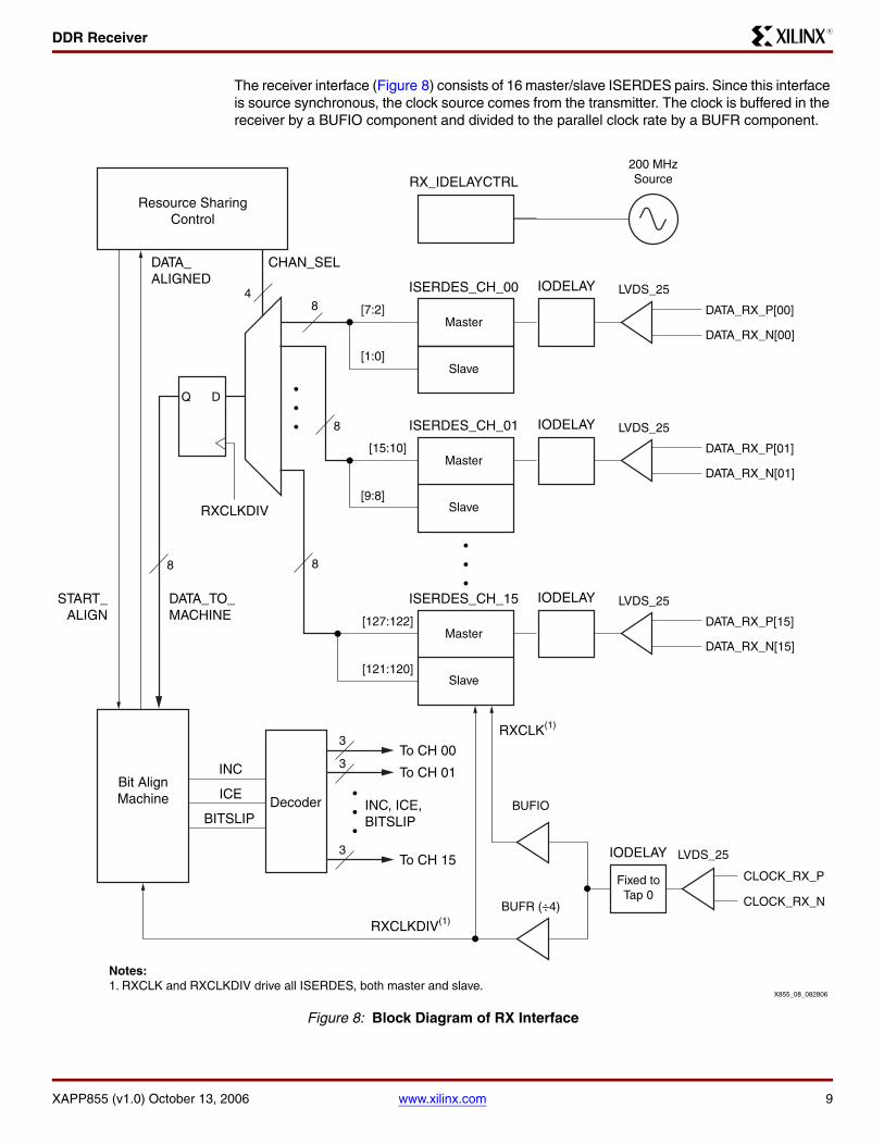
DDR Receiver
XAPP855 (v10) October 13 2006 wwwxilinxcom 9
R
The receiver interface (Figure 8) consists of 16 masterslave ISERDES pairs Since this interface is source synchronous the clock source comes from the transmitter The clock is buffered in the receiver by a BUFIO component and divided to the parallel clock rate by a BUFR component
Figure 8 Block Diagram of RX Interface
MasterDATA_RX_P[00]
DATA_RX_N[00]
LVDS_25
Slave
IODELAY
CHAN_SELDATA_ALIGNED
DATA_TO_MACHINE
RXCLK(1)
START_ALIGN
Master
LVDS_25
Slave
ISERDES_CH_01 IODELAY
X855_08_082806
DQ
BUFIO
BUFR (divide4)
8 [72]
[10]
[98]
[1510]
[127122]
[121120]
4
8
8 8
3
3
3
DATA_RX_P[01]
DATA_RX_N[01]
Master
LVDS_25
Slave
IODELAY
DATA_RX_P[15]
DATA_RX_N[15]
ISERDES_CH_15
ISERDES_CH_00
RXCLKDIV
INC
ICE
BITSLIP
RXCLKDIV(1)
INC ICEBITSLIP
To CH 15
To CH 01
To CH 00
RX_IDELAYCTRL
Resource SharingControl
Bit AlignMachine
200 MHzSource
LVDS_25
CLOCK_RX_N
CLOCK_RX_P
Notes1 RXCLK and RXCLKDIV drive all ISERDES both master and slave
IODELAY
Fixed to Tap 0
Decoder
DDR Receiver
XAPP855 (v10) October 13 2006 wwwxilinxcom 10
R
Each ISERDES in Figure 8 page 9 contributes 8 bits to the 128-bit parallel data bus Since there is only one instance of BIT_ALIGN_MACHINE in the receiver each data channel must be aligned separately by sharing that resource The 8-bit data buses from each ISERDES are fed into a MUX which selects which of the 16 channels has access to the BIT_ALIGN_MACHINE resource RESOURCE_SHARING_CONTROL controls the MUX to ensure that every channel completes its alignment before the MUX switches to the next channel The START_ALIGN signal tells the BIT_ALIGN_MACHINE that alignment can begin on the current channel because the MUX output is stable The DATA_ALIGNED signal tells the RESOURCE_SHARING_CONTROL module that alignment on the current channel is complete
The order of the parallel data outputs of the ISERDES is the opposite of the parallel data inputs of the OSERDES The least significant OSERDES data inputs are fed into the master while the least-significant ISERDES data outputs come from the slave (Figure 4 page 3 versus Figure 7)
The IDELAYCTRL module in Figure 8 is shown as having no connection to the rest of the receiver Actually IDELAYCTRL is required to calibrate the IODELAY blocks in the path of each data channel A single IDELAYCTRL block is sufficient to calibrate all 16 data channels since all channels are in the same bank
The BIT_ALIGN_MACHINE generates three control signals that adjust the timing of the appropriate ISERDES INC and ICE cause the IODELAY to increment or decrement the delay in the datapath by a fixed amount of ~75 ps (if a 200 MHz reference clock is used) BITSLIP causes each ISERDES to rotate the order of the parallel output data bits facilitating the process of word alignment These three control signals are directed to the appropriate ISERDES by the decoder shown in Figure 8 Although not shown in the figure the decoder is also controlled by the RESOURCE_SHARING_CONTROL module
Table 5 shows the device utilization statistics for the RX interface implemented in a Virtex-5 device These figures exclude the counters used to track the IODELAY settings on all data channels in most instances those counters can be removed after the interface is integrated and verified in a specific environment The majority of the LUTs utilized are consumed by the BIT_ALIGN_MACHINE which is the core of the receiver alignment algorithm As in the TX interface the RX interface consumes one BUFIO and one BUFR for clocking The clocking could also be accomplished using BUFGs and a DCM as described in ldquoInterface Clockingrdquo page 5 but the performanceconvenience trade off would need to be considered
Table 5 DDR RX Interface Utilization Statistics
Component Quantity Usage Description
Slice Flip-Flop 131 Multiple uses
Slice 105 Multiple uses
LUT 263 Multiple uses
IOB 34 17 LVDS input pairs (16 data 1 clock)
ISERDES 32 Master and slave ISERDES for every LVDS data pair
BUFIO 1 RXCLK
BUFR 1 RXCLKDIV
Receiver Interface Dynamic Timing
XAPP855 (v10) October 13 2006 wwwxilinxcom 11
R
Receiver Interface Dynamic Timing
The timing of the receiver interface is broken into two parts
bull The suboptimal timing inherent in the data and clock paths
bull The optimal timing created by the receiver when adjusting dynamic delays on each of the 16 data channels
Inherent Timing
An inventory of all propagation delays in the clock and datapaths must be taken to derive the inherent setuphold times The clock and datapaths for a single channel of this interface are shown in Figure 9 The ISE Timing Analyzer breaks down the paths into the timing parameters shown All components in the path have both a minimum and maximum value to account for process variations
Figure 10 page 12 shows the timing analyzer settings used to generate the information in this report Each of the timing parameters is described in Table 6 page 12 and Table 7 The minimum and maximum values of the individual timing parameters for the clock and datapaths are shown in Table 8 and Table 9 page 13
Note All raw timing numbers referenced in this document are subject to minor changes in subsequent revisions of the ISE tools
Figure 9 Timing Components of RX Data and Clock Paths
ISERDESFFsIODELAY
VariableInit to 0
DI O
CLK
IODELAYIBUFDS
IBUFDS
+
ndash
+
ndash Fixed toTap 0
I O
X855_09_082806
DataPath
ClockPath
TIOPI TIODDO_IDATAINTNET1 TNET2
TIOPI TIODDO_IDATAIN TISDCK_DDLY
TBUFIOCKO_O
BUFIO
Receiver Interface Dynamic Timing
XAPP855 (v10) October 13 2006 wwwxilinxcom 12
R
Figure 10 ISE Timing Analyzer Properties Used in this Document
Table 6 Datapath Timing Definitions
Timing Parameter Description
TIOPI Delay from the IOB pad through the LVDS input buffer to the I pin of the IOB pad
TIODDO_IDATAIN Delay from the I pin of IOB pad to the D input of the ISERDES
TISDCK_DDLY Delay from the D input of the ISERDES to the sampling registers in the ISERDES (setup and hold times of ISERDES)
Table 7 Clock Path Timing Definitions
Timing Parameter Description
TIOPI Delay from the IOB pad through the LVDS input buffer to the I pin of the IOB pad
TIODDO_IDATAIN Delay from I pin of IOB pad to the O output of the IODELAY block
TNET1 Delay from the O output of the IODELAY block to the I pin of BUFIO
TBUFIOCKO_O Clock to out delay of BUFIO
TNET2 Clock distribution delay from BUFIO output to the clock input of data ISERDES
Table 8 Datapath Delay Inventory for a -1 Speed Grade XC5VLX50T Device
Timing Parameter Maximum Datapath Delay Minimum Datapath Delay
TIOPI 1083 ns 0763 ns
TIODDO_IDATAIN 0671 ns 0671 ns
TISDCK_DDLY 0064 ns ndash0038 ns
TOTAL 1818 ns 1396 ns
XAPP855_10_071306
Receiver Interface Dynamic Timing
XAPP855 (v10) October 13 2006 wwwxilinxcom 13
R
According to the inherent timing prediction the data is going to arrive before the clock by an amount determined by Equation 1 and Equation 2 Equation 1 calculates that data arrives before the clock by at least 1076 ns in a -1 device Equation 2 calculates that data arrives before the clock by at most 2213 ns Equation 3 shows a timing window that covers all -1 devices under all conditions This timing window describes the inherent timing of the data and clock paths Assuming skew-matched PCB traces for all sixteen channels then it can be assumed that all 16 channels in the receiver have roughly the same timing window
Equation 1
Equation 2
Equation 3
Figure 11 shows the timing windows for all speed grades of an XC5VLX50T device as well as a hardware measurement of the inherent timing relationship (to validate the calculations) The hardware measurement shows the DDR interface data arriving 1425 ns before the clock which by inspection places the device in all three speed grade ranges (the device used for the hardware measurement is a -2 device)
Table 9 Clock Path Delay Inventory for a -1 Speed Grade XC5VLX50T Device
Timing Parameter Maximum Clock Path Delay Minimum Clock Path Delay
TIOPI 1150 ns 0820 ns
TIODDO_IDATAIN 0671 ns 0671 ns
TNET1 0254 ns 0190 ns
TBUFIOCKO_O 1130 ns 0894 ns
TNET2 0404 ns 0319 ns
TOTAL 3609 ns 2894 ns
Setup Time Max Data Delay Min Clock Delay 1818 2894ndash 1076 nsndash==ndash=
Hold Time Max Clock Delay Min Data Delay 3609 1396ndash 2213 ns==ndash=
Timing Window 2213 1076ndash 1137 ns==
Figure 11 Timing Windows Show Uncertainty in ClockData Relationship as Calculated by Timing Analyzer
400 Mbs Data (T = 25 ns)
1425 ns Hardware MeasurementData Arrives
x855_11_091806
-11076ns 2213 ns
-21043 ns 2039 ns
-30989 ns 1878 ns
Receiver Interface Dynamic Timing
XAPP855 (v10) October 13 2006 wwwxilinxcom 14
R
Dynamic Timing and BIT_ALIGN_MACHINE
In ldquoInherent Timingrdquo page 11 the inherent timing of the interface was calculated for all speed grades and validated with a hardware measurement In that case the inherent timing was sufficient because the data rate is only 400 Mbs (Figure 11 page 13) What happens when the data rate is increased such that the hold edge of the data window begins to shrink (Figure 12)
At 600 Mbs the inherent timing relationship is no longer adequate to meet timing because there are cases when the sampling clock edge is in the middle of the data transition As the data rates increase to 800 and 1000 Mbs the clock actually captures the data arriving one bit time later For designs that are sensitive to word alignment this is unacceptable
The solution to the suboptimal inherent timing is dynamic timing The BIT_ALIGN_MACHINE module in the receiver performs two functions of dynamic timing
bull Bit Alignment Position the sampling edge of the clock at the center of the data eye by adding delay to the datapaths
bull Word Alignment Ensure that the parallel data bits are in the correct order at the output of the ISERDES by using the bitslip function in the ISERDES
The steps of the bit-alignment procedure are shown in Figure 13 page 15 Each step of the algorithm can either add or subtract delay from the datapath All 16 channels are taken through this procedure independently This procedure measures one full data eye (in terms of 75 ps delay taps) and then returns to the center of the data eye Steps 1 and 2 are dedicated to moving through the partial eye of the initial timing while steps 3 and 4 are dedicated to measuring a full eye Step 5 is dedicated to positioning the clock edge at the center of the data eye
Figure 12 Inherent Timing Windows Shown in Relation to Multiple Data Rates
400 Mbs Data (T = 25 ns)
600 Mbs Data (T = 167 ns)
800 Mbs Data (T = 127 ns)
1000 Mbs Data (T = 10 ns)
-11076ns 2213 ns
-21043 ns 2039 ns
-30989 ns
1425 ns
1878 ns
Hardware MeasurementData Arrives
x855_12_091806
Receiver Interface Dynamic Timing
XAPP855 (v10) October 13 2006 wwwxilinxcom 15
R
Jitter is represented in Figure 13 as multiple transition lines Accounting for jitter is a crucial part of the algorithm In step 2 the first data transition is found If there is no jitter then the eye measurement can begin instantly after finding the transition However when jitter is considered the algorithm must find the first transition move through the transition and then begin looking for the second transition If the algorithm does not move through the first transition intelligently it runs the risk of falsely detecting the second transition
Once bit alignment is complete the order of the data bits can be adjusted to achieve word alignment The bit-alignment procedure ensures that data is being sampled correctly but the order of the data can be a few bits off from where the receiver expects it to be To correct this the bitslip feature of the ISERDES is used to slip bit times until the proper alignment is found For this feature to be useful a training pattern must be generated by the transmitter (as discussed in ldquoDDR Transmitterrdquo page 3) that the receiver can use to determine the proper word alignment In this reference design the training pattern is 00101100 (0x2C) This pattern is mostly arbitrary as many other patterns work just as well This pattern was chosen because a training pattern should behave electrically as much like real data as possible such that the center of the training eye is the center of the data eye Since real data contains strings of consecutive ones and zeros it is best for the training pattern to do the same For that reason a 0x2C pattern is better than an 0xAA pattern because it contains run lengths of 1 2 3 and 4 bit times
Table 10 page 16 shows the word-alignment process in the case where bit alignment completes with the data outputs set to 0x58 Since 0x58 is not the training pattern the receiver is looking for bitslip is asserted until 0x2C is found This reference design uses a 18 deserialization so there are only eight possible configurations of the parallel data outputs If bitslip is asserted infinitely the same eight configurations will repeat Bitslip in DDR mode is somewhat irregular because it does not simply rotate by one bit on every bitslip cycle This effect is inconsequential to the word-alignment procedure (see the Virtex-5 User Guide for more details)
Figure 13 Dynamic Bit-Alignment Procedure in BIT_ALIGN_MACHINE
Data 0
Data Arrives Before Clock
Data 1
x855_13_091806
Data 0 Data 1
Data 0 Data 1
Data 0 Data 1
Data 0 Data 1
Sampling Clock (Fixed Delay)
Return to Center of Eye
End Measuring Eye
Begin Measuring Eye
Find 1st Transition
Initial Timing1
2
3
4
5
Receiver Interface Dynamic Timing
XAPP855 (v10) October 13 2006 wwwxilinxcom 16
R
The FSM in the BIT_ALIGN_MACHINE module used to implement both bit and word alignment is shown in Figure 14 page 17 The FSM is divided into five sections loosely described as finding the first transition getting through the first transition finding the second transition returning to the center of the eye and word alignment
To get through the first transition effectively for all possible types of jitter two methods are used The first method pertains to random jitter If there is a lot of random jitter at the sampling point then the samples generated are not stable The algorithm detects this instability by comparing current samples to older samples and therefore knows where the transition begins and ends But what if the jitter is extremely deterministic The transition then has discreet crossing points such that within the transition there is very stable but incorrect data In this case the algorithm does not sense any instability and falsely concludes that the sampling point is not in the transition To address this case apart from evaluating stability the algorithm also evaluates the correctness of the data content by using the bitslip feature in the middle of the transition For example if the algorithm determines that the sampled data is stable it then asserts bitslip to look for the correct data If 0x2c is found within eight assertions of bitslip then the sampling point is not in the transition But if 0x2c is not found then the algorithm increments the data delay and repeats the transition test again
Table 10 Word Alignment in the DDR Receiver
Bitslip Cycle Data Value (Hex) Data Value (Bin) Description of Bitslip operation
1 58 0101 1000 ndash
2 0B 0000 1011 Rotate 3 bits to right
3 16 0001 0110 Rotate 1 bit to left
4 C2 1100 0010 Rotate 3 bits to right
5 85 1000 0101 Rotate 1 bit to left
6 B0 1011 0000 Rotate 3 bits to right
7 61 0110 0001 Rotate 1 bit to left
8 2C 0010 1100 Rotate 3 bits to right
Receiver Interface Dynamic Timing
XAPP855 (v10) October 13 2006 wwwxilinxcom 17
R
Figure 14 FSM in the BIT_ALIGN_MACHINE Module
TRANSITION_CHECK (01000)
First TransitionNot Detected
First TransitionNot Detected
First TransitionDetected
First TransitionDetected
Past the FirstTransition
Second TransitionNot Detected
Second TransitionDetected
Decrement DelayAgain
Bit AlignmentComplete
Still Samplingin Transition
INC_ONCE (01111)
SEARCH_PAT (01101)
IDLE (01100)
IDLE (10000)
RECHECK_TRANS (00010)
ONE_BITSLIP (00110)
INC_ONCE (01011)
WAIT_8_CYCLES (00100)
COUNT_1 (01110)
INC_ONCE (01001)
WAIT_8_CYCLES (00011)
IDLE (10010)
TRAINING_DONE (00111)
FIRST_SAMPLE (00001)
RESET (00000)
DEC_TO_HALF (01010)
WORD_ALIGN (00101)
X855_14_082806
Routine to Avoid False Detection of Second Transition
=CHECK_PATTERN
Receiver Interface Dynamic Timing
XAPP855 (v10) October 13 2006 wwwxilinxcom 18
R
Interface Timing Budget
In addition to sampling the data as closely as possible to the center of the data eye the actual size of the data eye is important By accurately predicting the size of the data eye in the receiver the overall performance ceiling of the interface can be inferred The ideal data eye width is the period of the data rate (for example TBit_Period = 100 ns for 1000 Mbs) Both the transmitter and receiver circuits have sources of error that subtract from the ideal data eye The equation for the eye width at the output of the transmitter is shown in Equation 4 TJITTER is the peak-to-peak jitter of the clock source driving the transmitter data bus and forwarded clock TDCD is the maximum duty cycle distortion of the clock tree driving the data bus and forwarded clock Skew is not considered in the transmitter or receiver because the receiver calibrates out skew between channels by performing alignment on each channel individually
Equation 4
Equation 5 calculates the width of the data eye at the receiver flip-flops Ideally the eye width at the receiver is the same as the eye width at the output of the transmitter but there are sources of error in the transmission medium and receiver circuitry Duty cycle distortion must be considered again on the receiver clock tree TSAMP_BUFIO is the receiver sampling error due to drift caused by voltage and temperature variations TIDELAYPAT_JIT is the amount of pattern dependent jitter that is accumulated in each tap of the IDELAY chain For a clock pattern TIDELAYPAT_JIT is 0 pstap peak to peak For a data pattern with long and short run lengths of zeroes and ones (simulated by PRBS23) TIDELAYPAT_JIT is a finite value that must be considered in the timing budget
Equation 5
TBOARD_JITTER includes jitter induced by receiver input capacitance and the parasitics of the physical data path on the PCB TBOARD_JITTER must be determined by simulation as it varies as a function of frequency and for receivers of different types and vendors On the ML550 with a -2 speed-grade Virtex-5 device the TBOARD_JITTER is measured at roughly 200 ps at 900 Mbs (assuming data content equivalent to PRBS23) TQUANTIZATION_ERR or quantization error is caused by the granularity of the IDELAY tap chain Working with 75 ps increments it is not possible to utilize the entire data eye since inevitably some valid eye width is lost between two taps The value for this loss is 75 ps As long as the receiver eye width calculated using Equation 5 is greater than or equal to 0 the interface operates correctly over process voltage and temperature
For example Equation 6 and Equation 7 show the timing budget calculation for the DDR interface running at 900 Mbs in a -2 speed grade device on an ML550 evaluation board Refer to the data sheet for the most current values The TX interface is looped back to the RX interface on the same Virtex-5 FPGA as shown in Equation 2
Equation 6
Equation 7
Changes in voltage and temperature cause the data channels of the interface to drift relative to the clock If the DDR interface were to transfer user data for a long period of time over all specified conditions of temperature and voltage Equation 7 states that there would be at least 107 ps (one or two IDELAY taps) of data window remaining valid during all fluctuations of temperature and voltage Compare this calculation to the measurements in Table 12 page 21 Case 900 Mbs There are four taps that are error free under all conditions In ldquoAppendixrdquo there are three -2 devices tested at 900 Mbs and each has 4 4 and 3 taps respectively that are error free under all conditions
DATA_EYE_WIDTH_TX TBIT_PERIOD TJITTERndash TDCD_BUFIOndash=
DATA_EYE_WIDTH_RX DATA_EYE_WIDTH_TX
TBOARD_JITTER
ndash
TSAMP_BUFIOndash TDCD_BUFIOndash
TIDELAYPAT_JIT IDELAY taps in datapathtimes[ ]ndash
TQUANTIZATION_ERRndash
=
DATA_EYE_WIDTH_TX 1111 ps 25 psndash 100 psndash 986 ps= =
DATA_EYE_WIDTH_RX986 ps 200 psndash 400 psndash 100 psndash 8 ps 13 tapstimes[ ] 75 ps 107 ps=ndashndash
=
Interface Characterization
XAPP855 (v10) October 13 2006 wwwxilinxcom 19
R
At a given temperature and voltage setting the data valid window is much larger because there is no drift when temperature and voltage are constant The size of the data valid window under constant conditions is 107 ps + TSAMP_BUFIO which in this case is at least 507 ps (six or seven IDELAY taps) Compare this calculation to the measurements of any single condition in Table 12 Case 900 Mbs In the worst case (ndash5 supply) there are 7 taps that are error free
Equation 8 and Equation 9 show the same timing budget calculation for the DDR interface running at 10 Gbs in a -2 speed grade device on an ML550 Evaluation Board
Equation 8
Equation 9
Equation 9 predicts that no data window remains valid during all specified fluctuations of temperature and voltage (compare to Table 12 Case 1000 Mbs) In ldquoAppendixrdquo there are three -2 devices tested at 1000 Mbs and each has 1 3 and 1 taps respectively that are error free under all conditions This data rate and device combination are very marginal cases
To operate at 10 Gbs the DDR interface requires additional circuitry to track out voltage-temperature variations in real-time (see XAPP860 16-channel DDR LVDS Interface with Real-time Window Monitoring for a DDR Interface with real-time window monitoring) If the voltage-temperature variations are removed from the picture the predicted data valid window is ndash120 ps + TSAMP_BUFIO which in this case is at least 280 ps (3 or 4 taps) Compare this calculation to the measurements of any single condition in Table 18 page 34 There are at least four error-free taps in all conditions
Interface Characterization
By following the procedure illustrated in Figure 13 page 15 the bit-alignment algorithm should never insert more than approximately 15 bit times of delay on the data channels The fewest number of delay taps should be used in the datapath because they produce a finite amount of degradation (TIDELAYPAT_JIT) The worst-case initial timing for the algorithm occurs when the clock samples just before the data transitions as in the 600 Mbs case in Figure 12 page 14 The algorithm must move all the way through the first eye to find the first transition (1 bit time) and then move halfway into the next eye to center the sampling point (05 bit time) This process produces a worst-case total delay insertion of 15 bit times
The actual performance of the bit-alignment algorithm is characterized as a function of data rate in Figure 15 page 20 For all data rates the expectation is that the tap settings of all 16 channels in the DDR receiver do not exceed approximately 15 bit times of delay Both the maximum and minimum tap setting of all 16 channels is recorded for each data rate This graph only shows the data for a single device Comparing the 15 bit time mask to the actual settings it is clear that the algorithm remains within the 15 bit time limit At 13 Gbs the tap setting actually exceeds the mask by one tap (a negligible violation)
DATA_EYE_WIDTH_TX 1000 ps 25 psndash 100 psndash 875 ps= =
DATA_EYE_WIDTH_RX 875 ps 300 psndash400 ps 100 psndash
ndash8 ps 15 tapstimes[ ] 75 ps 120 psndash=ndashndash
=
Interface Characterization
XAPP855 (v10) October 13 2006 wwwxilinxcom 20
R
The maximum and minimum tap settings in Figure 15 generally stay within 3 to 4 taps of each other except in the case of 640 Mbs and 1300 Mbs data rates These data rates are seams in the inherent timing At data rates below 640 Mbs the tap settings are in the range of 30 taps and at data rates above 640 Mbs the tap settings are in the range of 12 taps Referring back to Figure 12 page 14 it is clear why this seam occurs As the data rate increases past 600 Mbs the initial sampling point of the inherent timing moves into a different data eye creating a different starting point for the algorithm At 640 Mbs some of the 16 channels start in one eye while other channels start in the other eye Fortunately this is not an issue because the single bit time of difference between the channels is resolved using bitslip
Referring back to Figure 8 page 9 the clock channel goes through an IDELAY block with a default value of 0 Once the data rate is chosen for a given design this initial IDELAY value can be changed to a non-zero value to achieve more favorable inherent timing For example a design running at 620 Mbs can use 30 IDELAY taps on the delay channels each contributing a certain amount of jitter to the timing budget calculation By setting the initial clock delay to 5 taps the inherent timing moves across the seam shown in the 600 Mbs range of Figure 15 causing the data channels to only use about 12 IDELAY taps Only spectrally rich data patterns accumulate jitter in the IDELAY tap chain so the clock IDELAY can be set to any value without diminishing the timing budget This optimization is entirely optional and can be done once the design is running in hardware
The DDR receiver is designed to remove skew between channels by aligning each channel individually The ML550 board on which this reference design is characterized is designed to have minimal skew between channels However there is clearly a finite amount of skew between channels due to clock skew in the TX and RX BUFIO networks package skew and trace length tolerance on the ML550 board Table 11 page 21 shows how the bit-alignment algorithm sets the delay for each channel differently to compensate for skew between channels The table captures the range of settings among the 16 channels at specific data rates for a -2 device If there were additional skew among the 16 channels then the tap setting range would be larger to compensate for it The algorithm is designed such that skew between channels should not diminish the performance of the interface The range of tap settings differs for different devices and speed grades but the magnitude should be approximately the same
Figure 15 Bit-Alignment Algorithm Performance
60
50
40
30
20
10
0200 400 600 800 1000 1200 1400 1600
Data Rate (Mbs)
Del
ay T
ap U
tiliz
atio
n HW Measurement (Min)HW Measurement (Max)15 Bit Time Mask
X855_15_072406
Interface Characterization
XAPP855 (v10) October 13 2006 wwwxilinxcom 21
R
Since the receiver alignment logic only runs once immediately after reset the resulting dynamic timing must be adequate to ensure error-free operation over the specified voltage and temperature variations that can occur over time The data-valid window at the receiver input must be wide enough to withstand these variations (receiver drift) Table 12 page 21 shows the data-valid window at the ISERDES registers in the DDR receiver The eyes shown are collective eyes of all 16 channels The BERT testbench configuration loops back the DDR transmitter to the DDR receiver Using pattern generators and error detectors programmed to send and receive a pseudorandom bit sequence (PRBS23) the width of the data-valid window is evaluated using pseudorandom data that closely resembles real user data
Table 11 Tap Setting Range For Various Data Rates Measured on a -2 Device
Data Rate (Mbs) Tap Setting Range Compensated Skew
500 31ndash34 4 taps
600 28ndash30 3 taps
700 10ndash12 3 taps
800 11ndash13 3 taps
900 11ndash13 3 taps
1000 13ndash15 3 taps
1100 13ndash15 3 taps
1200 14ndash15 2 taps
Table 12 Measurement of Receiver Drift under Extreme Conditions for Multiple Data Rates
ConditionIODELAY Taps (1)
ndash8 ndash7 ndash6 ndash5 ndash4 ndash3 ndash2 ndash1 0 +1 +2 +3 +4 +5 +6 +7 +8
Case 800 Mbs
25degC Nom Supplies F F F P P P P P C P P P P P F F F
0degC Nom Supplies F F F P P P P P P P P P P P F F F
85degC Nom Supplies F F F P P P P P P P P P P P F F F
25degC +5 Supplies F P P P P P P P P P P P F F F F F
0degC +5 Supplies F P P P P P P P P P P P F F F F F
85degC +5 Supplies F P P P P P P P P P P P F F F F F
25degC ndash5 Supplies F F F F F F P P P P P P P P P F F
0degC ndash5 Supplies F F F F F F P P P P P P P P P P F
85degC ndash5 Supplies F F F F F P P P P P P P P P P F F
CONCLUSION Error free under all conditions when calibrated under nominal conditions to position C
Interface Characterization
XAPP855 (v10) October 13 2006 wwwxilinxcom 22
R
Case 900 Mbs
25degC Nom Supplies F F F F P P P P C P P P P F F F F
0degC Nom Supplies F F F F P P P P P P P P P F F F F
85degC Nom Supplies F F F F P P P P P P P P F F F F F
25degC +5 Supplies F F P P P P P P P P P F F F F F F
0degC +5 Supplies F F P P P P P P P P P F F F F F F
85degC +5 Supplies F F P P P P P P P P P F F F F F F
25degC ndash5 Supplies F F F F F F F P P P P P P P P F F
0degC ndash5 Supplies F F F F F F F P P P P P P P P F F
85degC ndash5 Supplies F F F F F F F P P P P P P P F F F
CONCLUSION Error free under all conditions when calibrated under nominal conditions to position C
Case 1000 Mbs
25degC Nom Supplies F F F F F P P P C P P P F F F F F
0degC Nom Supplies F F F F F P P P P P P P F F F F F
85degC Nom Supplies F F F F F P P P P P P P F F F F F
25degC +5 Supplies F F F P P P P P P P F F F F F F F
0degC +5 Supplies F F F P P P P P P P F F F F F F F
85degC +5 Supplies F F F P P P P P P P P F F F F F F
25degC ndash5 Supplies F F F F F F F F P P P P P P F F F
0degC ndash5 Supplies F F F F F F F F P P P P P P F F F
85degC ndash5 Supplies F F F F F F F F P P P P P P F F F
CONCLUSION Error free under all conditions when calibrated under nominal conditions to position C
Case 1100 Mbs
25degC Nom Supplies F F F F F P P P C P F F F F F F F
0degC Nom Supplies F F F F F P P P P P F F F F F F F
85degC Nom Supplies F F F F F P P P P P F F F F F F F
25degC +5 Supplies F F F P P P P P P F F F F F F F F
0degC +5 Supplies F F F P P P P P P F F F F F F F F
85degC +5 Supplies F F F P P P P P P F F F F F F F F
25degC ndash5 Supplies F F F F F F F F P P P P F F F F F
0degC ndash5 Supplies F F F F F F F F P P P P F F F F F
85degC ndash5 Supplies F F F F F F F F P P P P F F F F F
CONCLUSION Error free under all conditions when calibrated under nominal conditions to position C
Table 12 Measurement of Receiver Drift under Extreme Conditions for Multiple Data Rates (Continued)
ConditionIODELAY Taps (1)
ndash8 ndash7 ndash6 ndash5 ndash4 ndash3 ndash2 ndash1 0 +1 +2 +3 +4 +5 +6 +7 +8
Interface Characterization
XAPP855 (v10) October 13 2006 wwwxilinxcom 23
R
In all test cases shown in Table 12 page 21 the bit-align machine accurately places the sampling point in the center of the data eye (indicated by the C in each test case) In the 1100 Mbs case the bit-align machine places the sampling point slightly off center This slight inaccuracy occurs when the center of a real data pattern diverges from the center of the training pattern The electrical behavior of different data patterns is discussed below
After the dynamic timing is established for a given test case under nominal conditions the device is subjected to extremes of temperature and voltage to stress the receiver timing At data rates of 1100 Mbs and below the dynamic timing established after reset under nominal conditions is sufficient to meet timing over all specified extreme conditions (the column with the C passes traffic error free under all conditions) At a data rate of 1200 Mbs the design operates correctly under nominal conditions but the data-valid window is not large enough to withstand the voltage variations For this particular transmission medium the 1200 Mbs case requires a real-time adjustment circuit that could track the center of the eye
The full datapath of the testbench consists of
TX rarr 5 FR-4 rarr SAMTEC QSE Conn rarr 12 Ribbon Cable rarr SAMTEC QSE Conn rarr 5 FR-4 rarr RX
For shorter transmission media higher performance can be achieved in accordance with the section ldquoInterface Timing Budgetrdquo page 18 Interface performance is not solely a question of the LVDS driver performance specification but rather a question of adequate timing margin to withstand production and environmental variations From Table 12 the total amount of variation experienced over temperature and voltage is roughly 375 ps (5 taps at 75 ps per tap) This number should be comparable to the specification for receiver sampling error (TSAMP_BUFIO) shown in the Virtex-5 Data Sheet
Case 1200 Mbs
25degC Nom Supplies F F F F F F P P C P F F F F F F F
0degC Nom Supplies F F F F F F P P P P F F F F F F F
85degC Nom Supplies F F F F F F P P P F F F F F F F F
25degC +5 Supplies F F F F P P P P F F F F F F F F F
0degC +5 Supplies F F F P P P P P F F F F F F F F F
85degC +5 Supplies F F F F P P P P F F F F F F F F F
25degC ndash5 Supplies F F F F F F F F F P P P F F F F F
0degC ndash5 Supplies F F F F F F F F F P P P F F F F F
85degC ndash5 Supplies F F F F F F F F F P P F F F F F F
CONCLUSION Errors caused by plusmn5 variations in supply voltages
Notes 1 Where 0 is the reference tap determined by the bit-align machine under nominal conditions at 25degC2 P = Error-free transmission F = Error in transmission C = IODELAY tap position selected by bit-align machine under nominal conditions at 25degC3 Device under test is -2 speed grade
Table 12 Measurement of Receiver Drift under Extreme Conditions for Multiple Data Rates (Continued)
ConditionIODELAY Taps (1)
ndash8 ndash7 ndash6 ndash5 ndash4 ndash3 ndash2 ndash1 0 +1 +2 +3 +4 +5 +6 +7 +8
Interface Characterization
XAPP855 (v10) October 13 2006 wwwxilinxcom 24
R
Pattern Dependence of Receiver Performance
Different types of data patterns have different electrical signatures (rise and fall times jitter eye symmetry etc) A pattern with very narrow spectral content (such as a clock pattern) moves very favorably through the link because the receiver frequency response has little effect on the signal integrity However a pattern with wide spectral content (such as real data and pseudorandom patterns) stresses the links frequency response If the frequency response is not flat across the entire spectrum of the data content then the signal integrity is degraded as a result The amount of degradation measured is shown in Table 13 page 25 The DDR transmitter is looped back to the DDR receiver and different patterns are programmed to traverse the link Performance is assessed by evaluating the integrity of those patterns in the receiver
PRBS7 is a pseudorandom data pattern with a maximum run length of seven consecutive zeroes or ones PRBS15 is defined as having a maximum run length of fifteen consecutive zeroes or ones These limitations on run lengths limit the spectral content of the pattern A PRBS15 pattern has greater spectral content than a PRBS7 pattern and therefore is a more strenuous test for the link PRBS29 is the most strenuous test in Table 13 A clock pattern is effectively a PRBS1
As predicted Table 13 shows that there is more degradation for data patterns with more spectral content At 1000 Mbs and below the data eye closure is symmetrical Symmetrical eye closure is desired because it does not change the center of the eye as determined by the bit-alignment algorithm Above 1000 Mbs the eye closure becomes more asymmetrical causing the center of the data eye to diverge from the calibrated center (by only 1 tap)
In every data rate shown in Table 13 all significant pattern-dependent degradation is caused between PRBS1 (clock pat) and PRBS15 Between PRBS15 and PRBS29 there is no additional degradation recorded in any of the measurements
Interface Characterization
XAPP855 (v10) October 13 2006 wwwxilinxcom 25
R
Table 13 Link Performance for Various Types of Data Measured on a -2 Device
PatternIODELAY Taps (1)
ndash8 ndash7 ndash6 ndash5 ndash4 ndash3 ndash2 ndash1 0 +1 +2 +3 +4 +5 +6 +7 +8 +9
Case 600 Mbs
Clock Pat (0101) P P P P P P P P C P P P P P P P P P
Training Pat (0x2C) P P P P P P P P C P P P P P P P P F
PRBS7 P P P P P P P P C P P P P P P P P F
PRBS15 F P P P P P P P C P P P P P P P F F
PRBS23 F P P P P P P P C P P P P P P P F F
PRBS29 F P P P P P P P C P P P P P P P F F
Case 800 Mbs
Clock Pat (0101) F F P P P P P P C P P P P P P F F F
Training Pat (0x2C) F F P P P P P P C P P P P P P F F F
PRBS7 F F P P P P P P C P P P P P F F F F
PRBS15 F F F P P P P P C P P P P P F F F F
PRBS23 F F F P P P P P C P P P P P F F F F
PRBS29 F F F P P P P P C P P P P P F F F F
Case 1000 Mbs
Clock Pat (0101) F F F P P P P P C P P P P P F F F F
Training Pat (0x2C) F F F P P P P P C P P P P F F F F F
PRBS7 F F F F P P P P C P P P F F F F F F
PRBS15 F F F F F P P P C P P P F F F F F F
PRBS23 F F F F F P P P C P P P F F F F F F
PRBS29 F F F F F P P P C P P P F F F F F F
Case 1200 Mbs
Clock Pat (0101) F F F F P P P P C P P P P F F F F F
Training Pat (0x2C) F F F F P P P P C P P P F F F F F F
PRBS7 F F F F F P P P C P F F F F F F F F
PRBS15 F F F F F F P P C F F F F F F F F F
PRBS23 F F F F F F P P C F F F F F F F F F
PRBS29 F F F F F F P P C F F F F F F F F F
Case 1400 Mbs
Clock Pat (0101) F F F F F F P P C P P P F F F F F F
Training Pat (0x2C) F F F F F P P P C P P F F F F F F F
PRBS7 F F F F F F F P C P F F F F F F F F
PRBS15 F F F F F F F P C F F F F F F F F F
PRBS23 F F F F F F F P C F F F F F F F F F
PRBS29 F F F F F F F P C F F F F F F F F F
Notes 1 Where 0 is the reference tap determined by the bit-align machine under nominal conditions at 25degC2 P = Error-free transmission F = Error in transmission C = IODELAY tap position selected by bit-align machine under nominal conditions at 25degC
Resetting the Interface
XAPP855 (v10) October 13 2006 wwwxilinxcom 26
R
Resetting the Interface
Several dependencies determine the order in which circuits should be reset in the interface The receiver cannot begin the alignment algorithm if the transmitter is not sending the training pattern The transmitter must be reset before the receiver and time must be allowed for the training pattern to propagate across the link before the receiver comes out of reset The receiver also cannot begin the alignment algorithm until IDELAYCTRL has recovered from reset which could takes hundreds of cycles The recommended reset timing for the interface is shown in Figure 16 This reset timing is implemented in the BERT testbench for this interface
The TX reset (RST_TX) is used to reset all TX circuitry and also IDELAYCTRL The IDELAYCTRL reset is asynchronous so driving it with RST_TX is acceptable The minimum pulse width of IDELAYCTRL reset is 50 ns (TIDELAYCTRL_RPW) For that reason resets are held High for 16 clock cycles The RX reset (RST_RX) is used to reset all RX circuitry and is asserted when the IDELAYCTRL READY flag goes High indicating that the IODELAY blocks are calibrated
The timing of the READY flag in Figure 16 is a potential hazard Most likely it is High during a TX reset because it takes many cycles for IDELAYCTRL to deassert the READY flag It is easy to make the mistake of resetting the receiver too early To avoid this hazard the RX reset should be asserted only after seeing a deassertion and reassertion of the READY flag
Conclusion Based on the design and characterization described in this document the 16-Channel DDR reference design operates to the performance targets in Table 14 under all conditions of process voltage and temperature However to meet these targets over voltage and temperature the timing budget must be guaranteed according to the analysis in ldquoInterface Timing Budgetrdquo See ldquoAppendixrdquo page 27 for further justification of the maximum performance recommendations in Table 14
Figure 16 Recommended Interface Reset Timing
RST_TX
IDELAYCTRLREADY
RST_RX
16 Cycles X855_16_072406
Table 14 Performance of 16-Channel DDR Interface
Speed Grade Maximum Performance
-1 800 Mbs
-2 900 Mbs
-3 10 Gbs(1)
Notes 1 To achieve higher performance (up to 125 Gbs) see 16-channel DDR LVDS Interface with Realtime
Window Monitoring for an example of a DDR interface with real-time window monitoring
Appendix
XAPP855 (v10) October 13 2006 wwwxilinxcom 27
R
Appendix Performance Characterization Data
Refer to ldquoInterface Characterizationrdquo page 19 for explanations about how to interpret the data in the ldquoAppendixrdquo These tables show collective data eyes for the entire interface over process voltage and temperature (PVT) Three devices from each speed grade were selected for this characterization
The calibrated center position of the eye (marked by the C in the tables below) varies slightly from channel to channel (due to small skews between channels) That range is referred to as center tap range Analysis of Table 16 page 28 through Table 20 page 40 shows that the center tap range for slow and fast parts differ significantly at the same data rate (because the BIT_ALIGN_MACHINE algorithm adjusts for differences in speed)
All data in the ldquoAppendixrdquo is collected using the BERT testbench shown in Figure 2 page 2 The data pattern is PRBS23 and the devicepackage is XC5VLX50T-FF1136 The transmission path for the cases shown in Table 16 through Table 20 is repeated for convenience
TX rarr 5 FR-4 rarr SAMTEC QSE Conn rarr 12 Ribbon Cable rarr SAMTEC QSE Conn rarr 5 FR-4 rarr RX
A summary of these characterization results is shown in Table 15 Each of the nine parts were tested at 800 900 1000 1100 and 1200 Mbs When the interface is error free on all channels under all extreme conditions of temperature and voltage the particular test case is designated by a P A test case is marked FAIL when the interface suffered errors on any channel under any particular condition of voltage and temperature
Table 15 Summary of Interface Characterization Results
Device (SN) Speed Grade 800 Mbs 900 Mbs 1000Mbs 1100 Mbs 1200 Mbs
2194 -1 P P P FAIL FAIL
2219 -1 P FAIL FAIL FAIL FAIL
2199 -1 P P FAIL FAIL FAIL
001 -2 P P FAIL P FAIL
002 -2 P P P P FAIL
003 -2 P P FAIL FAIL FAIL
004 -3 P P P P P
005 -3 P P P P P
006 -3 P P P P P
Appendix
XAPP855 (v10) October 13 2006 wwwxilinxcom 28
R
Table 16 Measurement of Receiver Drift under Extreme Conditions at 800 Mbs
ConditionIODELAY Taps (1)
ndash8 ndash7 ndash6 ndash5 ndash4 ndash3 ndash2 ndash1 0 +1 +2 +3 +4 +5 +6 +7 +8
SN 2194 Speed Grade -1
25degC Nom Supplies F F F P P P P P C P P P P F F F F
0degC Nom Supplies F F F P P P P P P P P P P F F F F
85degC Nom Supplies F F F F P P P P P P P P P F F F F
25degC +5 Supplies F F P P P P P P P P P P F F F F F
0degC +5 Supplies F F P P P P P P P P P P F F F F F
85degC +5 Supplies F F P P P P P P P P P P F F F F F
25degC ndash5 Supplies F F F F F F P P P P P P P P P F F
0degC ndash5 Supplies F F F F F F P P P P P P P P P F F
85degC ndash5 Supplies F F F F F F P P P P P P P P P F F
Center Tap Range Taps 11ndash12
CONCLUSION Error free under all conditions when calibrated under nominal conditions to position C
SN 2219 Speed Grade -1
25degC Nom Supplies F F F P P P P P C P P P F F F F F
0degC Nom Supplies F F F P P P P P P P P P F F F F F
85degC Nom Supplies F F F P P P P P P P P P F F F F F
25degC +5 Supplies F P P P P P P P P P P F F F F F F
0degC +5 Supplies F P P P P P P P P P P F F F F F F
85degC +5 Supplies F P P P P P P P P P P F F F F F F
25degC ndash5 Supplies F F F F F F P P P P P P P P F F F
0degC ndash5 Supplies F F F F F F F P P P P P P P F F F
85degC ndash5 Supplies F F F F F F P P P P P P P P F F F
Center Tap Range Taps 13ndash16
CONCLUSION Error free under all conditions when calibrated under nominal conditions to position C
SN 2199 Speed Grade -1
25degC Nom Supplies F F F P P P P P C P P P P F F F F
0degC Nom Supplies F F F P P P P P P P P P P F F F F
85degC Nom Supplies F F F P P P P P P P P P P F F F F
25degC +5 Supplies F P P P P P P P P P P P F F F F F
0degC +5 Supplies F P P P P P P P P P P P F F F F F
85degC +5 Supplies F P P P P P P P P P P P F F F F F
25degC ndash5 Supplies F F F F F F P P P P P P P P P F F
0degC ndash5 Supplies F F F F F F P P P P P P P P P F F
85degC ndash5 Supplies F F F F F F P P P P P P P P P F F
Center Tap Range Taps 10ndash12
CONCLUSION Error free under all conditions when calibrated under nominal conditions to position C
Appendix
XAPP855 (v10) October 13 2006 wwwxilinxcom 29
R
SN 001 Speed Grade -2
25degC Nom Supplies F F F P P P P P C P P P P F F F F
0degC Nom Supplies F F F P P P P P P P P P P F F F F
85degC Nom Supplies F F F P P P P P P P P P P F F F F
25degC +5 Supplies F P P P P P P P P P P P F F F F F
0degC +5 Supplies F P P P P P P P P P P F F F F F F
85degC +5 Supplies F P P P P P P P P P P P F F F F F
25degC ndash5 Supplies F F F F F P P P P P P P P P P F F
0degC ndash5 Supplies F F F F F P P P P P P P P P P F F
85degC ndash5 Supplies F F F F F P P P P P P P P P P F F
Center Tap Range Taps 10ndash12
CONCLUSION Error free under all conditions when calibrated under nominal conditions to position C
SN 002 Speed Grade -2
25degC Nom Supplies F F F P P P P P C P P P P F F F F
0degC Nom Supplies F F F P P P P P P P P P P F F F F
85degC Nom Supplies F F F P P P P P P P P P P F F F F
25degC +5 Supplies F P P P P P P P P P P P F F F F F
0degC +5 Supplies F P P P P P P P P P P P F F F F F
85degC +5 Supplies F F P P P P P P P P P P F F F F F
25degC ndash5 Supplies F F F F F P P P P P P P P P P F F
0degC ndash5 Supplies F F F F F P P P P P P P P P P F F
85degC ndash5 Supplies F F F F F P P P P P P P P P P F F
Center Tap Range Taps 10ndash12
CONCLUSION Error free under all conditions when calibrated under nominal conditions to position C
SN 003 Speed Grade -2
25degC Nom Supplies F F F P P P P P C P P P P F F F F
0degC Nom Supplies F F F P P P P P P P P P P F F F F
85degC Nom Supplies F F F P P P P P P P P P P F F F F
25degC +5 Supplies F P P P P P P P P P P P F F F F F
0degC +5 Supplies F P P P P P P P P P P F F F F F F
85degC +5 Supplies F P P P P P P P P P P P F F F F F
25degC ndash5 Supplies F F F F F F P P P P P P P P P F F
0degC ndash5 Supplies F F F F F F P P P P P P P P P F F
85degC ndash5 Supplies F F F F F F P P P P P P P P P F F
Center Tap Range Taps 11ndash13
CONCLUSION Error free under all conditions when calibrated under nominal conditions to position C
Table 16 Measurement of Receiver Drift under Extreme Conditions at 800 Mbs (Continued)
ConditionIODELAY Taps (1)
ndash8 ndash7 ndash6 ndash5 ndash4 ndash3 ndash2 ndash1 0 +1 +2 +3 +4 +5 +6 +7 +8
Appendix
XAPP855 (v10) October 13 2006 wwwxilinxcom 30
R
SN 004 Speed Grade -3
25degC Nom Supplies F F F P P P P P C P P P P F F F F
0degC Nom Supplies F F F P P P P P P P P P F F F F F
85degC Nom Supplies F F F P P P P P P P P P P F F F F
25degC +5 Supplies F P P P P P P P P P P P F F F F F
0degC +5 Supplies F P P P P P P P P P P P F F F F F
85degC +5 Supplies F F P P P P P P P P P P F F F F F
25degC ndash5 Supplies F F F F F P P P P P P P P P F F F
0degC ndash5 Supplies F F F F F P P P P P P P P P F F F
85degC ndash5 Supplies F F F F F P P P P P P P P P F F F
Center Tap Range Taps 8ndash9 23ndash24
CONCLUSION Error free under all conditions when calibrated under nominal conditions to position C
SN 005 Speed Grade -3
25degC Nom Supplies F F P P P P P P C P P P P F F F F
0degC Nom Supplies F F P P P P P P P P P P P F F F F
85degC Nom Supplies F F F P P P P P P P P P P P F F F
25degC +5 Supplies F P P P P P P P P P P P F F F F F
0degC +5 Supplies F P P P P P P P P P P P F F F F F
85degC +5 Supplies F P P P P P P P P P P P F F F F F
25degC ndash5 Supplies F F F F P P P P P P P P P P P F F
0degC ndash5 Supplies F F F F P P P P P P P P P P P F F
85degC ndash5 Supplies F F F F P P P P P P P P P P P F F
Center Tap Range Taps 9ndash10
CONCLUSION Error free under all conditions when calibrated under nominal conditions to position C
SN 006 Speed Grade -3
25degC Nom Supplies F F P P P P P P C P P P P F F F F
0degC Nom Supplies F F P P P P P P P P P P P F F F F
85degC Nom Supplies F F F P P P P P P P P P P F F F F
25degC +5 Supplies F P P P P P P P P P P P F F F F F
0degC +5 Supplies F P P P P P P P P P P P F F F F F
85degC +5 Supplies F F P P P P P P P P P P F F F F F
25degC ndash5 Supplies F F F P P P P P P P P P P P F F F
0degC ndash5 Supplies F F F P P P P P P P P P P P F F F
85degC ndash5 Supplies F F F F F P P P P P P P P P F F F
Center Tap Range Taps 8ndash9 23ndash24
CONCLUSION Error free under all conditions when calibrated under nominal conditions to position C
Notes 1 IODELAY taps where 0 is the reference tap determined by the bit align machine at nominal voltage and 25degC2 P = Error-free transmission F = Error in transmission C = IODELAY tap position selected by bit-align machine under nominal conditions at 25degC
Table 16 Measurement of Receiver Drift under Extreme Conditions at 800 Mbs (Continued)
ConditionIODELAY Taps (1)
ndash8 ndash7 ndash6 ndash5 ndash4 ndash3 ndash2 ndash1 0 +1 +2 +3 +4 +5 +6 +7 +8
Appendix
XAPP855 (v10) October 13 2006 wwwxilinxcom 31
R
Table 17 Measurement of Receiver Drift under Extreme Conditions at 900 Mbs
ConditionIODELAY Taps (1)
ndash8 ndash7 ndash6 ndash5 ndash4 ndash3 ndash2 ndash1 0 +1 +2 +3 +4 +5 +6 +7 +8
SN 2194 Speed Grade -1
25degC Nom Supplies F F F F F P P P C P P P F F F F F
0degC Nom Supplies F F F F F P P P P P P P F F F F F
85degC Nom Supplies F F F F F P P P P P P P P F F F F
25degC +5 Supplies F F F P P P P P P P P F F F F F F
0degC +5 Supplies F F F P P P P P P P P F F F F F F
85degC +5 Supplies F F F P P P P P P P P F F F F F F
25degC ndash5 Supplies F F F F F F F P P P P P P P F F F
0degC ndash5 Supplies F F F F F F F P P P P P P P F F F
85degC ndash5 Supplies F F F F F F F P P P P P P P F F F
Center Tap Range Taps 11ndash12
CONCLUSION Error free under all conditions when calibrated under nominal conditions to position C
SN 2219 Speed Grade -1
25degC Nom Supplies F F F F F P P P C P P P F F F F F
0degC Nom Supplies F F F F F P P P P P P P F F F F F
85degC Nom Supplies F F F F F P P P P P P P F F F F F
25degC +5 Supplies F F F P P P P P P P F F F F F F F
0degC +5 Supplies F F F P P P P P P P F F F F F F F
85degC +5 Supplies F F F P P P P P P P F F F F F F F
25degC ndash5 Supplies F F F F F F F F F P P P P P F F F
0degC ndash5 Supplies F F F F F F F F F P P P P P F F F
85degC ndash5 Supplies F F F F F F F F P P P P P P F F F
Center Tap Range Taps 12ndash15
CONCLUSION Errors caused by ndash5 variation in supply voltage
SN 2199 Speed Grade -1
25degC Nom Supplies F F F F F P P P C P P P F F F F F
0degC Nom Supplies F F F F F P P P P P P P F F F F F
85degC Nom Supplies F F F F F P P P P P P P F F F F F
25degC +5 Supplies F F F P P P P P P P P F F F F F F
0degC +5 Supplies F F F P P P P P P P P F F F F F F
85degC +5 Supplies F F F P P P P P P P P F F F F F F
25degC ndash5 Supplies F F F F F F F F P P P P P P F F F
0degC ndash5 Supplies F F F F F F F F P P P P P P F F F
85degC ndash5 Supplies F F F F F F F F P P P P P P F F F
Center Tap Range Taps 10ndash12
CONCLUSION Error free under all conditions when calibrated under nominal conditions to position C
Appendix
XAPP855 (v10) October 13 2006 wwwxilinxcom 32
R
SN 001 Speed Grade -2
25degC Nom Supplies F F F F P P P P C P P P P F F F F
0degC Nom Supplies F F F F P P P P P P P P P F F F F
85degC Nom Supplies F F F F F P P P P P P P P F F F F
25degC +5 Supplies F F P P P P P P P P P F F F F F F
0degC +5 Supplies F F P P P P P P P P P F F F F F F
85degC +5 Supplies F F F P P P P P P P P P F F F F F
25degC ndash5 Supplies F F F F F F F P P P P P P P F F F
0degC ndash5 Supplies F F F F F F F P P P P P P P F F F
85degC ndash5 Supplies F F F F F F F P P P P P P P F F F
Center Tap Range Taps 9ndash11
CONCLUSION Error free under all conditions when calibrated under nominal conditions to position C
SN 002 Speed Grade -2
25degC Nom Supplies F F F F P P P P C P P P P F F F F
0degC Nom Supplies F F F F P P P P P P P P F F F F F
85degC Nom Supplies F F F F F P P P P P P P P F F F F
25degC +5 Supplies F F F P P P P P P P P F F F F F F
0degC +5 Supplies F F F P P P P P P P P F F F F F F
85degC +5 Supplies F F F P P P P P P P P P F F F F F
25degC ndash5 Supplies F F F F F F F P P P P P P P F F F
0degC ndash5 Supplies F F F F F F F P P P P P P P F F F
85degC ndash5 Supplies F F F F F F F P P P P P P P F F F
Center Tap Range Taps 10ndash12
CONCLUSION Error free under all conditions when calibrated under nominal conditions to position C
SN 003 Speed Grade -2
25degC Nom Supplies F F F F F P P P C P P P P F F F F
0degC Nom Supplies F F F F F P P P P P P P P F F F F
85degC Nom Supplies F F F F F P P P P P P P P F F F F
25degC +5 Supplies F F P P P P P P P P P F F F F F F
0degC +5 Supplies F F P P P P P P P P P F F F F F F
85degC +5 Supplies F F F P P P P P P P P F F F F F F
25degC ndash5 Supplies F F F F F F F P P P P P P P F F F
0degC ndash5 Supplies F F F F F F F F P P P P P P F F F
85degC ndash5 Supplies F F F F F F F P P P P P P P F F F
Center Tap Range Taps 11ndash13
CONCLUSION Error free under all conditions when calibrated under nominal conditions to position C
Table 17 Measurement of Receiver Drift under Extreme Conditions at 900 Mbs (Continued)
ConditionIODELAY Taps (1)
ndash8 ndash7 ndash6 ndash5 ndash4 ndash3 ndash2 ndash1 0 +1 +2 +3 +4 +5 +6 +7 +8
Appendix
XAPP855 (v10) October 13 2006 wwwxilinxcom 33
R
SN 004 Speed Grade -3
25degC Nom Supplies F F F F P P P P C P P P P F F F F
0degC Nom Supplies F F F P P P P P P P P P P F F F F
85degC Nom Supplies F F F F P P P P P P P P P F F F F
25degC +5 Supplies F F F P P P P P P P P P F F F F F
0degC +5 Supplies F F F P P P P P P P P P F F F F F
85degC +5 Supplies F F F P P P P P P P P P F F F F F
25degC ndash5 Supplies F F F F F F P P P P P P P P F F F
0degC ndash5 Supplies F F F F F F P P P P P P P P F F F
85degC ndash5 Supplies F F F F F F P P P P P P P P F F F
Center Tap Range Taps 7ndash8
CONCLUSION Error free under all conditions when calibrated under nominal conditions to position C
SN 005 Speed Grade ndash3
25degC Nom Supplies F F F P P P P P C P P P P F F F F
0degC Nom Supplies F F F P P P P P P P P P P F F F F
85degC Nom Supplies F F F F P P P P P P P P P F F F F
25degC +5 Supplies F F P P P P P P P P P P F F F F F
0degC +5 Supplies F F P P P P P P P P P P F F F F F
85degC +5 Supplies F F F P P P P P P P P P F F F F F
25degC ndash5 Supplies F F F F F F P P P P P P P P F F F
0degC ndash5 Supplies F F F F F P P P P P P P P P F F F
85degC ndash5 Supplies F F F F F F P P P P P P P P F F F
Center Tap Range Taps 9ndash10
CONCLUSION Error free under all conditions when calibrated under nominal conditions to position C
SN 006 Speed Grade -3
25degC Nom Supplies F F F F P P P P C P P P P F F F F
0degC Nom Supplies F F F F P P P P P P P P P F F F F
85degC Nom Supplies F F F F P P P P P P P P P F F F F
25degC +5 Supplies F F P P P P P P P P P P F F F F F
0degC +5 Supplies F F P P P P P P P P P P F F F F F
85degC +5 Supplies F F F P P P P P P P P P F F F F F
25degC ndash5 Supplies F F F F F P P P P P P P P P F F F
0degC ndash5 Supplies F F F F F P P P P P P P P P F F F
85degC ndash5 Supplies F F F F F F P P P P P P P P F F F
Center Tap Range Taps 7ndash8
CONCLUSION Error free under all conditions when calibrated under nominal conditions to position C
Notes 1 IODELAY taps where 0 is the reference tap determined by the bit align machine at nominal voltage and 25degC2 P = Error-free transmission F = Error in transmission C = IODELAY tap position selected by bit-align machine under nominal conditions at 25degC
Table 17 Measurement of Receiver Drift under Extreme Conditions at 900 Mbs (Continued)
ConditionIODELAY Taps (1)
ndash8 ndash7 ndash6 ndash5 ndash4 ndash3 ndash2 ndash1 0 +1 +2 +3 +4 +5 +6 +7 +8
Appendix
XAPP855 (v10) October 13 2006 wwwxilinxcom 34
R
Table 18 Measurement of Receiver Drift under Extreme Conditions at 1000 Mbs
ConditionIODELAY Taps (1)
ndash8 ndash7 ndash6 ndash5 ndash4 ndash3 ndash2 ndash1 0 +1 +2 +3 +4 +5 +6 +7 +8
SN 2194 Speed Grade -1
25degC Nom Supplies F F F F F P P P C P P F F F F F F
0degC Nom Supplies F F F F F P P P P P P F F F F F F
85degC Nom Supplies F F F F F P P P P P P F F F F F F
25degC +5 Supplies F F F P P P P P P P F F F F F F F
0degC +5 Supplies F F F P P P P P P P F F F F F F F
85degC +5 Supplies F F F F P P P P P P F F F F F F F
25degC ndash5 Supplies F F F F F F F F P P P P P F F F F
0degC ndash5 Supplies F F F F F F F F P P P P P F F F F
85degC ndash5 Supplies F F F F F F F F P P P P P F F F F
Center Tap Range Taps 12ndash13
CONCLUSION Error free under all conditions when calibrated under nominal conditions to position C
SN 2219 Speed Grade -1
25degC Nom Supplies F F F F F F P P C P P F F F F F F
0degC Nom Supplies F F F F F F P P P P P F F F F F F
85degC Nom Supplies F F F F F F P P P P P F F F F F F
25degC +5 Supplies F F F P P P P P P F F F F F F F F
0degC +5 Supplies F F F P P P P P P F F F F F F F F
85degC +5 Supplies F F F F P P P P P F F F F F F F F
25degC ndash5 Supplies F F F F F F F F F P P P P F F F F
0degC ndash5 Supplies F F F F F F F F F F P P P F F F F
85degC ndash5 Supplies F F F F F F F F F P P P P F F F F
Center Tap Range Taps 14ndash17
CONCLUSION Errors caused by ndash5 variation in supply voltage
SN 2199 Speed Grade -1
25degC Nom Supplies F F F F F F P P C P P F F F F F F
0degC Nom Supplies F F F F F F P P P P P F F F F F F
85degC Nom Supplies F F F F F F P P P P P F F F F F F
25degC +5 Supplies F F F F P P P P P P F F F F F F F
0degC +5 Supplies F F F F P P P P P P F F F F F F F
85degC +5 Supplies F F F F P P P P P P F F F F F F F
25degC ndash5 Supplies F F F F F F F F F P P P P F F F F
0degC ndash5 Supplies F F F F F F F F F P P P P F F F F
85degC ndash5 Supplies F F F F F F F F F P P P P F F F F
Center Tap Range Taps 12ndash14
CONCLUSION Errors caused by ndash5 variation in supply voltage
Appendix
XAPP855 (v10) October 13 2006 wwwxilinxcom 35
R
SN 001 Speed Grade -2
25degC Nom Supplies F F F F F F P P C P P P F F F F F
0degC Nom Supplies F F F F F F P P P P P P F F F F F
85degC Nom Supplies F F F F F F P P P P P P F F F F F
25degC +5 Supplies F F F F P P P P P P F F F F F F F
0degC +5 Supplies F F F F P P P P P P F F F F F F F
85degC +5 Supplies F F F F P P P P P P P F F F F F F
25degC ndash5 Supplies F F F F F F F F F P P P P F F F F
0degC ndash5 Supplies F F F F F F F F F P P P P F F F F
85degC ndash5 Supplies F F F F F F F F F P P P P F F F F
Center Tap Range Taps 11ndash12
CONCLUSION Errors caused by ndash5 variation in supply voltage
SN 002 Speed Grade -2
25degC Nom Supplies F F F F F P P P C P P F F F F F F
0degC Nom Supplies F F F F F P P P P P P P F F F F F
85degC Nom Supplies F F F F F P P P P P P P F F F F F
25degC +5 Supplies F F F F P P P P P P F F F F F F F
0degC +5 Supplies F F F P P P P P P P F F F F F F F
85degC +5 Supplies F F F F P P P P P P P F F F F F F
25degC ndash5 Supplies F F F F F F F P P P P P P F F F F
0degC ndash5 Supplies F F F F F F F P P P P P P F F F F
85degC ndash5 Supplies F F F F F F F P P P P P P F F F F
Center Tap Range Taps 11ndash13
CONCLUSION Error free under all conditions when calibrated under nominal conditions to position C
SN 003 Speed Grade -2
25degC Nom Supplies F F F F F F P P C P P F F F F F F
0degC Nom Supplies F F F F F F P P P P P F F F F F F
85degC Nom Supplies F F F F F F P P P P P F F F F F F
25degC +5 Supplies F F F F P P P P P P F F F F F F F
0degC +5 Supplies F F F F P P P P P P F F F F F F F
85degC +5 Supplies F F F F P P P P P P F F F F F F F
25degC ndash5 Supplies F F F F F F F F F P P P P F F F F
0degC ndash5 Supplies F F F F F F F F F P P P P F F F F
85degC ndash5 Supplies F F F F F F F F F P P P P F F F F
Center Tap Range Taps 13ndash14
CONCLUSION Errors caused by ndash5 variation in supply voltage
Table 18 Measurement of Receiver Drift under Extreme Conditions at 1000 Mbs (Continued)
ConditionIODELAY Taps (1)
ndash8 ndash7 ndash6 ndash5 ndash4 ndash3 ndash2 ndash1 0 +1 +2 +3 +4 +5 +6 +7 +8
Appendix
XAPP855 (v10) October 13 2006 wwwxilinxcom 36
R
SN 004 Speed Grade -3
25degC Nom Supplies F F F F F P P P C P P P F F F F F
0degC Nom Supplies F F F F F P P P P P P P F F F F F
85degC Nom Supplies F F F F F P P P P P P P F F F F F
25degC +5 Supplies F F F P P P P P P P P F F F F F F
0degC +5 Supplies F F F P P P P P P P P F F F F F F
85degC +5 Supplies F F F F P P P P P P P P F F F F F
25degC ndash5 Supplies F F F F F F F P P P P P P F F F F
0degC ndash5 Supplies F F F F F F F P P P P P P F F F F
85degC ndash5 Supplies F F F F F F F P P P P P P P F F F
Center Tap Range Taps 9ndash10
CONCLUSION Error free under all conditions when calibrated under nominal conditions to position C
SN 005 Speed Grade -3
25degC Nom Supplies F F F F P P P P C P P P F F F F F
0degC Nom Supplies F F F F P P P P P P P P F F F F F
85degC Nom Supplies F F F F P P P P P P P P F F F F F
25degC +5 Supplies F F F P P P P P P P P F F F F F F
0degC +5 Supplies F F P P P P P P P P P F F F F F F
85degC +5 Supplies F F F P P P P P P P P F F F F F F
25degC ndash5 Supplies F F F F F F P P P P P P P P F F F
0degC ndash5 Supplies F F F F F F P P P P P P P P F F F
85degC ndash5 Supplies F F F F F F P P P P P P P F F F F
Center Tap Range Taps 11ndash12
CONCLUSION Error free under all conditions when calibrated under nominal conditions to position C
SN 006 Speed Grade -3
25degC Nom Supplies F F F F P P P P C P P P F F F F F
0degC Nom Supplies F F F F P P P P P P P P F F F F F
85degC Nom Supplies F F F F P P P P P P P P F F F F F
25degC +5 Supplies F F F P P P P P P P P F F F F F F
0degC +5 Supplies F F F P P P P P P P P F F F F F F
85degC +5 Supplies F F F P P P P P P P P F F F F F F
25degC ndash5 Supplies F F F F F F P P P P P P P F F F F
0degC ndash5 Supplies F F F F F F P P P P P P P F F F F
85degC ndash5 Supplies F F F F F F P P P P P P P F F F F
Center Tap Range Taps 9ndash10
CONCLUSION Error free under all conditions when calibrated under nominal conditions to position C
Notes 1 IODELAY taps where 0 is the reference tap determined by the bit align machine at nominal voltage and 25degC2 P = Error-free transmission F = Error in transmission C = IODELAY tap position selected by bit-align machine under nominal conditions at 25degC
Table 18 Measurement of Receiver Drift under Extreme Conditions at 1000 Mbs (Continued)
ConditionIODELAY Taps (1)
ndash8 ndash7 ndash6 ndash5 ndash4 ndash3 ndash2 ndash1 0 +1 +2 +3 +4 +5 +6 +7 +8
Appendix
XAPP855 (v10) October 13 2006 wwwxilinxcom 37
R
Table 19 Measurement of Receiver Drift under Extreme Conditions at 1100 Mbs
ConditionIODELAY Taps (1)
ndash8 ndash7 ndash6 ndash5 ndash4 ndash3 ndash2 ndash1 0 +1 +2 +3 +4 +5 +6 +7 +8
SN 2194 Speed Grade -1
25degC Nom Supplies F F F F F F P P C P P F F F F F F
0degC Nom Supplies F F F F F F P P P P P F F F F F F
85degC Nom Supplies F F F F F F P P P P P F F F F F F
25degC +5 Supplies F F F F P P P P P F F F F F F F F
0degC +5 Supplies F F F F P P P P P F F F F F F F F
85degC +5 Supplies F F F F P P P P P F F F F F F F F
25degC ndash5 Supplies F F F F F F F F F P P P F F F F F
0degC ndash5 Supplies F F F F F F F F F P P P F F F F F
85degC ndash5 Supplies F F F F F F F F F P P P F F F F F
Center Tap Range Taps 13ndash14
CONCLUSION Errors caused by ndash5 variation in supply voltage
SN 2219 Speed Grade -1
25degC Nom Supplies F F F F F F P P C P F F F F F F F
0degC Nom Supplies F F F F F F P P P P F F F F F F F
85degC Nom Supplies F F F F F F P P P P F F F F F F F
25degC +5 Supplies F F F F P P P P F F F F F F F F F
0degC +5 Supplies F F F F P P P P F F F F F F F F F
85degC +5 Supplies F F F F P P P P F F F F F F F F F
25degC ndash5 Supplies F F F F F F F F F F P P F F F F F
0degC ndash5 Supplies F F F F F F F F F F P P F F F F F
85degC ndash5 Supplies F F F F F F F F F P P P F F F F F
Center Tap Range Taps 6 15ndash17
CONCLUSION Errors caused by plusmn5 variation in supply voltage
SN 2199 Speed Grade -1
25degC Nom Supplies F F F F F F F P C P F F F F F F F
0degC Nom Supplies F F F F F F F P P P F F F F F F F
85degC Nom Supplies F F F F F F F P P P F F F F F F F
25degC +5 Supplies F F F F P P P P P F F F F F F F F
0degC +5 Supplies F F F F P P P P P F F F F F F F F
85degC +5 Supplies F F F F F P P P P F F F F F F F F
25degC ndash5 Supplies F F F F F F F F F F P P F F F F F
0degC ndash5 Supplies F F F F F F F F F F P P F F F F F
85degC ndash5 Supplies F F F F F F F F F F P P F F F F F
Center Tap Range Taps 13ndash15
CONCLUSION Errors caused by ndash5 variation in supply voltage
Appendix
XAPP855 (v10) October 13 2006 wwwxilinxcom 38
R
SN 001 Speed Grade -2
25degC Nom Supplies F F F F F F P P C P P F F F F F F
0degC Nom Supplies F F F F F F P P P P P F F F F F F
85degC Nom Supplies F F F F F F P P P P P F F F F F F
25degC +5 Supplies F F F F P P P P P F F F F F F F F
0degC +5 Supplies F F F F P P P P P F F F F F F F F
85degC +5 Supplies F F F F P P P P P F F F F F F F F
25degC ndash5 Supplies F F F F F F F F P P P P F F F F F
0degC ndash5 Supplies F F F F F F F F P P P P F F F F F
85degC ndash5 Supplies F F F F F F F F P P P P F F F F F
Center Tap Range Taps 12ndash13
CONCLUSION Error free under all conditions when calibrated under nominal conditions to position C
SN 002 Speed Grade -2
25degC Nom Supplies F F F F F P P P C P F F F F F F F
0degC Nom Supplies F F F F F P P P P P F F F F F F F
85degC Nom Supplies F F F F F F P P P P F F F F F F F
25degC +5 Supplies F F F F P P P P P F F F F F F F F
0degC +5 Supplies F F F P P P P P P F F F F F F F F
85degC +5 Supplies F F F F P P P P P F F F F F F F F
25degC ndash5 Supplies F F F F F F F F P P P P F F F F F
0degC ndash5 Supplies F F F F F F F F P P P P F F F F F
85degC ndash5 Supplies F F F F F F F F P P P P F F F F F
Center Tap Range Taps 13ndash14
CONCLUSION Error free under all conditions when calibrated under nominal conditions to position C
SN 003 Speed Grade -2
25degC Nom Supplies F F F F F F F P C P F F F F F F F
0degC Nom Supplies F F F F F F F P P P F F F F F F F
85degC Nom Supplies F F F F F F F P P P P F F F F F F
25degC +5 Supplies F F F F F P P P P F F F F F F F F
0degC +5 Supplies F F F F F P P P P F F F F F F F F
85degC +5 Supplies F F F F F P P P P F F F F F F F F
25degC ndash5 Supplies F F F F F F F F F F P P F F F F F
0degC ndash5 Supplies F F F F F F F F F F P P F F F F F
85degC ndash5 Supplies F F F F F F F F F P P P F F F F F
Center Tap Range Taps 14ndash16
CONCLUSION Errors caused by ndash5 variation in supply voltage
Table 19 Measurement of Receiver Drift under Extreme Conditions at 1100 Mbs (Continued)
ConditionIODELAY Taps (1)
ndash8 ndash7 ndash6 ndash5 ndash4 ndash3 ndash2 ndash1 0 +1 +2 +3 +4 +5 +6 +7 +8
Appendix
XAPP855 (v10) October 13 2006 wwwxilinxcom 39
R
SN 004 Speed Grade -3
25degC Nom Supplies F F F F F P P P C P P F F F F F F
0degC Nom Supplies F F F F F P P P P P P F F F F F F
85degC Nom Supplies F F F F F F P P P P P F F F F F F
25degC +5 Supplies F F F F P P P P P P F F F F F F F
0degC +5 Supplies F F F F P P P P P P F F F F F F F
85degC +5 Supplies F F F F P P P P P P F F F F F F F
25degC ndash5 Supplies F F F F F F F F P P P P F F F F F
0degC ndash5 Supplies F F F F F F F P P P P P F F F F F
85degC ndash5 Supplies F F F F F F F F P P P P P F F F F
Center Tap Range Taps 9ndash10
CONCLUSION Error free under all conditions when calibrated under nominal conditions to position C
SN 005 Speed Grade -3
25degC Nom Supplies F F F F F P P P C P P F F F F F F
0degC Nom Supplies F F F F F P P P P P P F F F F F F
85degC Nom Supplies F F F F F F P P P P P F F F F F F
25degC +5 Supplies F F F F P P P P P P F F F F F F F
0degC +5 Supplies F F F F P P P P P P F F F F F F F
85degC +5 Supplies F F F F P P P P P P F F F F F F F
25degC ndash5 Supplies F F F F F F F P P P P P P F F F F
0degC ndash5 Supplies F F F F F F F P P P P P P F F F F
85degC ndash5 Supplies F F F F F F F P P P P P P F F F F
Center Tap Range Taps 11ndash12
CONCLUSION Error free under all conditions when calibrated under nominal conditions to position C
SN 006 Speed Grade -3
25degC Nom Supplies F F F F F P P P C P P P F F F F F
0degC Nom Supplies F F F F F P P P P P P F F F F F F
85degC Nom Supplies F F F F F P P P P P P P F F F F F
25degC +5 Supplies F F F F P P P P P P P F F F F F F
0degC +5 Supplies F F F P P P P P P P F F F F F F F
85degC +5 Supplies F F F F P P P P P P P F F F F F F
25degC ndash5 Supplies F F F F F F P P P P P P P F F F F
0degC ndash5 Supplies F F F F F F P P P P P P P F F F F
85degC ndash5 Supplies F F F F F F F P P P P P P F F F F
Center Tap Range Taps 9ndash10
CONCLUSION Error free under all conditions when calibrated under nominal conditions to position C
Notes 1 IODELAY taps where 0 is the reference tap determined by the bit align machine at nominal voltage and 25degC2 P = Error-free transmission F = Error in transmission C = IODELAY tap position selected by bit-align machine under nominal conditions at 25degC
Table 19 Measurement of Receiver Drift under Extreme Conditions at 1100 Mbs (Continued)
ConditionIODELAY Taps (1)
ndash8 ndash7 ndash6 ndash5 ndash4 ndash3 ndash2 ndash1 0 +1 +2 +3 +4 +5 +6 +7 +8
Appendix
XAPP855 (v10) October 13 2006 wwwxilinxcom 40
R
Table 20 Measurement of Receiver Drift under Extreme Conditions at 1200 Mbs
ConditionIODELAY Taps (1)
ndash8 ndash7 ndash6 ndash5 ndash4 ndash3 ndash2 ndash1 0 +1 +2 +3 +4 +5 +6 +7 +8
SN 2194 Speed Grade -1
25degC Nom Supplies F F F F F F F P C F F F F F F F F
0degC Nom Supplies F F F F F F F P P F F F F F F F F
85degC Nom Supplies F F F F F F F P P F F F F F F F F
25degC +5 Supplies F F F F P P P P F F F F F F F F F
0degC +5 Supplies F F F F P P P P F F F F F F F F F
85degC +5 Supplies F F F F F P P P F F F F F F F F F
25degC ndash5 Supplies F F F F F F F F F P P F F F F F F
0degC ndash5 Supplies F F F F F F F F F F P F F F F F F
85degC ndash5 Supplies F F F F F F F F F P F F F F F F F
Center Tap Range Taps 13ndash15
CONCLUSION Errors caused by plusmn5 variation in supply voltage
SN 2219 Speed Grade -1
25degC Nom Supplies F F F F F F F F C F F F F F F F F
0degC Nom Supplies F F F F F F F P P F F F F F F F F
85degC Nom Supplies F F F F F F F F P F F F F F F F F
25degC +5 Supplies F F F F F P P P F F F F F F F F F
0degC +5 Supplies F F F F F P P P F F F F F F F F F
85degC +5 Supplies F F F F F F P P F F F F F F F F F
25degC ndash5 Supplies F F F F F F F F F F F F F F F F F
0degC ndash5 Supplies F F F F F F F F F F F F F F F F F
85degC ndash5 Supplies F F F F F F F F F F F F F F F F F
Center Tap Range Taps 6ndash7 16ndash17
CONCLUSION Errors caused by plusmn5 variation in supply voltage
SN 2199 Speed Grade -1
25degC Nom Supplies F F F F F F F P C F F F F F F F F
0degC Nom Supplies F F F F F F F P P F F F F F F F F
85degC Nom Supplies F F F F F F F F P F F F F F F F F
25degC +5 Supplies F F F F F P P P F F F F F F F F F
0degC +5 Supplies F F F F F P P P F F F F F F F F F
85degC +5 Supplies F F F F F P P P F F F F F F F F F
25degC ndash5 Supplies F F F F F F F F F F F F F F F F F
0degC ndash5 Supplies F F F F F F F F F F F F F F F F F
85degC ndash5 Supplies F F F F F F F F F F F F F F F F F
Center Tap Range Taps 13ndash15
CONCLUSION Errors caused by plusmn5 variation in supply voltage
Appendix
XAPP855 (v10) October 13 2006 wwwxilinxcom 41
R
SN 001 Speed Grade -2
25degC Nom Supplies F F F F F F F P C P F F F F F F F
0degC Nom Supplies F F F F F F F P P P F F F F F F F
85degC Nom Supplies F F F F F F F P P P F F F F F F F
25degC +5 Supplies F F F F F P P P P F F F F F F F F
0degC +5 Supplies F F F F P P P P P F F F F F F F F
85degC +5 Supplies F F F F F P P P P F F F F F F F F
25degC ndash5 Supplies F F F F F F F F F F P F F F F F F
0degC ndash5 Supplies F F F F F F F F F F P F F F F F F
85degC ndash5 Supplies F F F F F F F F F F P F F F F F F
Center Tap Range Taps 12ndash13
CONCLUSION Errors caused by ndash5 variation in supply voltage
SN 002 Speed Grade -2
25degC Nom Supplies F F F F F F P P C P F F F F F F F
0degC Nom Supplies F F F F F F P P P P F F F F F F F
85degC Nom Supplies F F F F F F F P P P F F F F F F F
25degC +5 Supplies F F F F P P P P F F F F F F F F F
0degC +5 Supplies F F F F P P P P F F F F F F F F F
85degC +5 Supplies F F F F F P P P F F F F F F F F F
25degC ndash5 Supplies F F F F F F F F P P P F F F F F F
0degC ndash5 Supplies F F F F F F F F P P P F F F F F F
85degC ndash5 Supplies F F F F F F F F F P P F F F F F F
Center Tap Range Taps 13ndash14
CONCLUSION Errors caused by plusmn5 variation in supply voltage
SN 003 Speed Grade -2
25degC Nom Supplies F F F F F F F P C F F F F F F F F
0degC Nom Supplies F F F F F F F P P F F F F F F F F
85degC Nom Supplies F F F F F F F F P F F F F F F F F
25degC +5 Supplies F F F F F P P P F F F F F F F F F
0degC +5 Supplies F F F F F P P P F F F F F F F F F
85degC +5 Supplies F F F F F F P P F F F F F F F F F
25degC ndash5 Supplies F F F F F F F F F F F F F F F F F
0degC ndash5 Supplies F F F F F F F F F F F F F F F F F
85degC ndash5 Supplies F F F F F F F F F F F F F F F F F
Center Tap Range Taps 14ndash15
CONCLUSION Errors caused by plusmn5 variation in supply voltage
Table 20 Measurement of Receiver Drift under Extreme Conditions at 1200 Mbs (Continued)
ConditionIODELAY Taps (1)
ndash8 ndash7 ndash6 ndash5 ndash4 ndash3 ndash2 ndash1 0 +1 +2 +3 +4 +5 +6 +7 +8
Appendix
XAPP855 (v10) October 13 2006 wwwxilinxcom 42
R
SN 004 Speed Grade -3
25degC Nom Supplies F F F F F F P P C P F F F F F F F
0degC Nom Supplies F F F F F P P P P P F F F F F F F
85degC Nom Supplies F F F F F F P P P P F F F F F F F
25degC +5 Supplies F F F F P P P P P F F F F F F F F
0degC +5 Supplies F F F F P P P P P F F F F F F F F
85degC +5 Supplies F F F F F P P P P F F F F F F F F
25degC ndash5 Supplies F F F F F F F F P P P F F F F F F
0degC ndash5 Supplies F F F F F F F F P P P F F F F F F
85degC ndash5 Supplies F F F F F F F F P P P F F F F F F
Center Tap Range Taps 9ndash11
CONCLUSION Error free under all conditions when calibrated under nominal conditions to position C
SN 005 Speed Grade -3
25degC Nom Supplies F F F F F P P P C P F F F F F F F
0degC Nom Supplies F F F F F P P P P P F F F F F F F
85degC Nom Supplies F F F F F F P P P P F F F F F F F
25degC +5 Supplies F F F F P P P P P F F F F F F F F
0degC +5 Supplies F F F P P P P P P F F F F F F F F
85degC +5 Supplies F F F F P P P P P F F F F F F F F
25degC ndash5 Supplies F F F F F F F P P P P P F F F F F
0degC ndash5 Supplies F F F F F F F P P P P P F F F F F
85degC ndash5 Supplies F F F F F F F F P P P F F F F F F
Center Tap Range Taps 11ndash13
CONCLUSION Error free under all conditions when calibrated under nominal conditions to position C
SN 006 Speed Grade -3
25degC Nom Supplies F F F F F P P P C P F F F F F F F
0degC Nom Supplies F F F F F P P P P P F F F F F F F
85degC Nom Supplies F F F F F P P P P P F F F F F F F
25degC +5 Supplies F F F P P P P P P F F F F F F F F
0degC +5 Supplies F F F P P P P P P F F F F F F F F
85degC +5 Supplies F F F F P P P P P F F F F F F F F
25degC ndash5 Supplies F F F F F F F P P P P F F F F F F
0degC ndash5 Supplies F F F F F F P P P P P F F F F F F
85degC ndash5 Supplies F F F F F F F P P P P F F F F F F
Center Tap Range Taps 10ndash11
CONCLUSION Error free under all conditions when calibrated under nominal conditions to position C
Notes 1 IODELAY taps where 0 is the reference tap determined by the bit align machine at nominal voltage and 25degC2 P = Error-free transmission F = Error in transmission C = IODELAY tap position selected by bit-align machine under nominal conditions at 25degC
Table 20 Measurement of Receiver Drift under Extreme Conditions at 1200 Mbs (Continued)
ConditionIODELAY Taps (1)
ndash8 ndash7 ndash6 ndash5 ndash4 ndash3 ndash2 ndash1 0 +1 +2 +3 +4 +5 +6 +7 +8
Revision History
XAPP855 (v10) October 13 2006 wwwxilinxcom 43
R
Revision History
The following table shows the revision history for this document
Date Version Revision
101306 10 Initial Xilinx release
- 16-Channel DDR LVDS Interface with Per-Channel Alignment
-
- Summary
- Introduction
-
- Figure 1 Full-Duplex 16-Channel DDR Link between a Virtex-5 Device and Another Device with a 16-Channel DDR Interface
- Figure 2 BERT Testbench for Hardware Verification of the DDR Interface
- Figure 3 Design Hierarchy of the Interface (TX and RX)
-
- DDR Transmitter
-
- Table 1 DDR_8TO1_16CHAN_TX Module Port Definitions
- Figure 4 MasterSlave OSERDES Pair for a Single Data Channel with 81 Serialization
- Figure 5 Block Diagram of TX Interface
- Table 2 DDR TX Interface Utilization Statistics
-
- Interface Clocking
-
- Figure 6 Global and Regional Clocking Schemes in Virtex-5 FPGAs
- Table 3 Comparison of Global and IO Clock Performance by Speed Grade
-
- DDR Receiver
-
- Table 4 DDR_8TO1_16CHAN_RX Module Port Definitions
- Figure 7 MasterSlave ISERDES Pair for a Single Data Channel with 18 Deserialization
- Figure 8 Block Diagram of RX Interface
- Table 5 DDR RX Interface Utilization Statistics
-
- Receiver Interface Dynamic Timing
-
- Inherent Timing
-
- Figure 9 Timing Components of RX Data and Clock Paths
- Figure 10 ISE Timing Analyzer Properties Used in this Document
- Table 6 Datapath Timing Definitions
- Table 7 Clock Path Timing Definitions
- Table 8 Datapath Delay Inventory for a -1 Speed Grade XC5VLX50T Device
- Table 9 Clock Path Delay Inventory for a -1 Speed Grade XC5VLX50T Device
- Figure 11 Timing Windows Show Uncertainty in ClockData Relationship as Calculated by Timing Analyzer
-
- Dynamic Timing and BIT_ALIGN_MACHINE
-
- Figure 12 Inherent Timing Windows Shown in Relation to Multiple Data Rates
- Figure 13 Dynamic Bit-Alignment Procedure in BIT_ALIGN_MACHINE
- Table 10 Word Alignment in the DDR Receiver
- Figure 14 FSM in the BIT_ALIGN_MACHINE Module
-
- Interface Timing Budget
-
- Interface Characterization
-
- Figure 15 Bit-Alignment Algorithm Performance
- Table 11 Tap Setting Range For Various Data Rates Measured on a -2 Device
- Table 12 Measurement of Receiver Drift under Extreme Conditions for Multiple Data Rates
- Pattern Dependence of Receiver Performance
-
- Table 13 Link Performance for Various Types of Data Measured on a -2 Device
-
- Resetting the Interface
-
- Figure 16 Recommended Interface Reset Timing
-
- Conclusion
-
- Table 14 Performance of 16-Channel DDR Interface
-
- Appendix
-
- Performance Characterization Data
-
- Table 15 Summary of Interface Characterization Results
- Table 16 Measurement of Receiver Drift under Extreme Conditions at 800 Mbs
- Table 17 Measurement of Receiver Drift under Extreme Conditions at 900 Mbs
- Table 18 Measurement of Receiver Drift under Extreme Conditions at 1000 Mbs
- Table 19 Measurement of Receiver Drift under Extreme Conditions at 1100 Mbs
- Table 20 Measurement of Receiver Drift under Extreme Conditions at 1200 Mbs
-
- Revision History
-
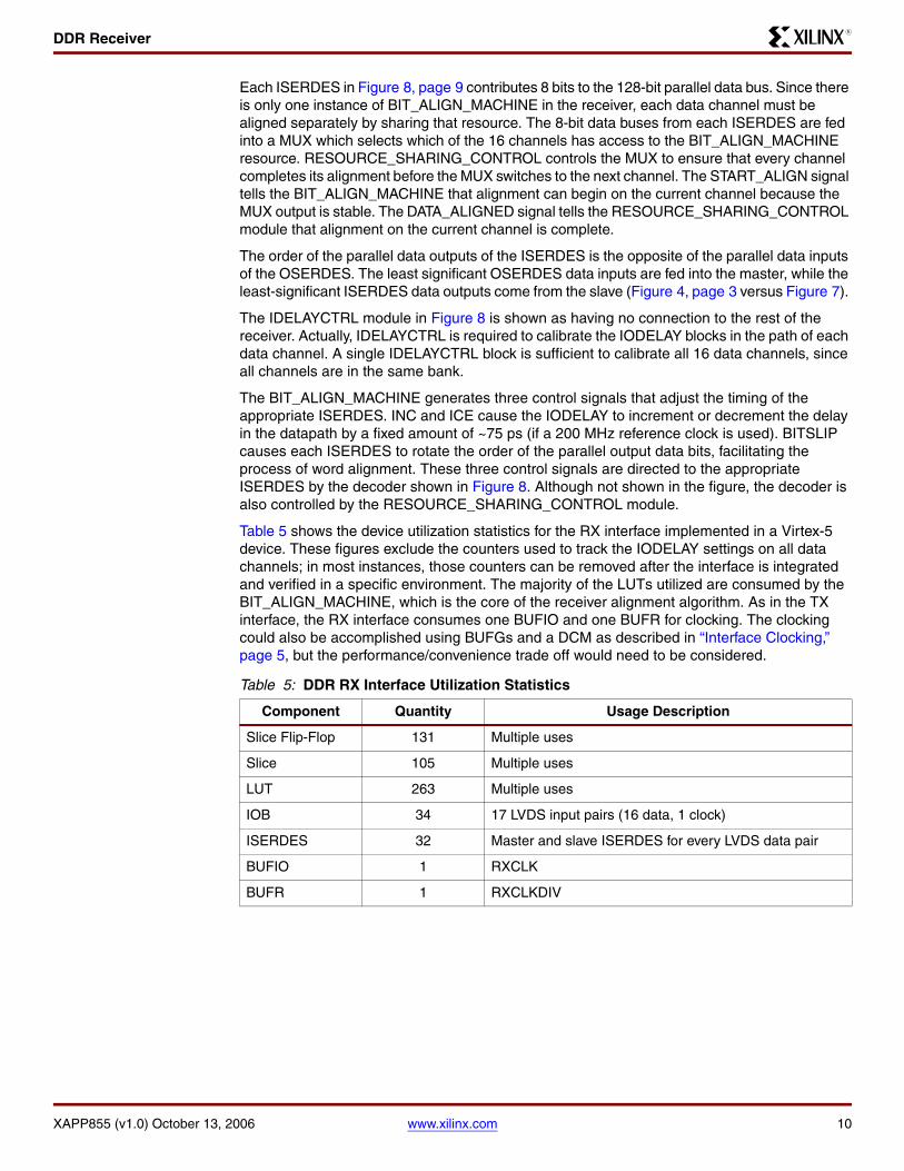
DDR Receiver
XAPP855 (v10) October 13 2006 wwwxilinxcom 10
R
Each ISERDES in Figure 8 page 9 contributes 8 bits to the 128-bit parallel data bus Since there is only one instance of BIT_ALIGN_MACHINE in the receiver each data channel must be aligned separately by sharing that resource The 8-bit data buses from each ISERDES are fed into a MUX which selects which of the 16 channels has access to the BIT_ALIGN_MACHINE resource RESOURCE_SHARING_CONTROL controls the MUX to ensure that every channel completes its alignment before the MUX switches to the next channel The START_ALIGN signal tells the BIT_ALIGN_MACHINE that alignment can begin on the current channel because the MUX output is stable The DATA_ALIGNED signal tells the RESOURCE_SHARING_CONTROL module that alignment on the current channel is complete
The order of the parallel data outputs of the ISERDES is the opposite of the parallel data inputs of the OSERDES The least significant OSERDES data inputs are fed into the master while the least-significant ISERDES data outputs come from the slave (Figure 4 page 3 versus Figure 7)
The IDELAYCTRL module in Figure 8 is shown as having no connection to the rest of the receiver Actually IDELAYCTRL is required to calibrate the IODELAY blocks in the path of each data channel A single IDELAYCTRL block is sufficient to calibrate all 16 data channels since all channels are in the same bank
The BIT_ALIGN_MACHINE generates three control signals that adjust the timing of the appropriate ISERDES INC and ICE cause the IODELAY to increment or decrement the delay in the datapath by a fixed amount of ~75 ps (if a 200 MHz reference clock is used) BITSLIP causes each ISERDES to rotate the order of the parallel output data bits facilitating the process of word alignment These three control signals are directed to the appropriate ISERDES by the decoder shown in Figure 8 Although not shown in the figure the decoder is also controlled by the RESOURCE_SHARING_CONTROL module
Table 5 shows the device utilization statistics for the RX interface implemented in a Virtex-5 device These figures exclude the counters used to track the IODELAY settings on all data channels in most instances those counters can be removed after the interface is integrated and verified in a specific environment The majority of the LUTs utilized are consumed by the BIT_ALIGN_MACHINE which is the core of the receiver alignment algorithm As in the TX interface the RX interface consumes one BUFIO and one BUFR for clocking The clocking could also be accomplished using BUFGs and a DCM as described in ldquoInterface Clockingrdquo page 5 but the performanceconvenience trade off would need to be considered
Table 5 DDR RX Interface Utilization Statistics
Component Quantity Usage Description
Slice Flip-Flop 131 Multiple uses
Slice 105 Multiple uses
LUT 263 Multiple uses
IOB 34 17 LVDS input pairs (16 data 1 clock)
ISERDES 32 Master and slave ISERDES for every LVDS data pair
BUFIO 1 RXCLK
BUFR 1 RXCLKDIV
Receiver Interface Dynamic Timing
XAPP855 (v10) October 13 2006 wwwxilinxcom 11
R
Receiver Interface Dynamic Timing
The timing of the receiver interface is broken into two parts
bull The suboptimal timing inherent in the data and clock paths
bull The optimal timing created by the receiver when adjusting dynamic delays on each of the 16 data channels
Inherent Timing
An inventory of all propagation delays in the clock and datapaths must be taken to derive the inherent setuphold times The clock and datapaths for a single channel of this interface are shown in Figure 9 The ISE Timing Analyzer breaks down the paths into the timing parameters shown All components in the path have both a minimum and maximum value to account for process variations
Figure 10 page 12 shows the timing analyzer settings used to generate the information in this report Each of the timing parameters is described in Table 6 page 12 and Table 7 The minimum and maximum values of the individual timing parameters for the clock and datapaths are shown in Table 8 and Table 9 page 13
Note All raw timing numbers referenced in this document are subject to minor changes in subsequent revisions of the ISE tools
Figure 9 Timing Components of RX Data and Clock Paths
ISERDESFFsIODELAY
VariableInit to 0
DI O
CLK
IODELAYIBUFDS
IBUFDS
+
ndash
+
ndash Fixed toTap 0
I O
X855_09_082806
DataPath
ClockPath
TIOPI TIODDO_IDATAINTNET1 TNET2
TIOPI TIODDO_IDATAIN TISDCK_DDLY
TBUFIOCKO_O
BUFIO
Receiver Interface Dynamic Timing
XAPP855 (v10) October 13 2006 wwwxilinxcom 12
R
Figure 10 ISE Timing Analyzer Properties Used in this Document
Table 6 Datapath Timing Definitions
Timing Parameter Description
TIOPI Delay from the IOB pad through the LVDS input buffer to the I pin of the IOB pad
TIODDO_IDATAIN Delay from the I pin of IOB pad to the D input of the ISERDES
TISDCK_DDLY Delay from the D input of the ISERDES to the sampling registers in the ISERDES (setup and hold times of ISERDES)
Table 7 Clock Path Timing Definitions
Timing Parameter Description
TIOPI Delay from the IOB pad through the LVDS input buffer to the I pin of the IOB pad
TIODDO_IDATAIN Delay from I pin of IOB pad to the O output of the IODELAY block
TNET1 Delay from the O output of the IODELAY block to the I pin of BUFIO
TBUFIOCKO_O Clock to out delay of BUFIO
TNET2 Clock distribution delay from BUFIO output to the clock input of data ISERDES
Table 8 Datapath Delay Inventory for a -1 Speed Grade XC5VLX50T Device
Timing Parameter Maximum Datapath Delay Minimum Datapath Delay
TIOPI 1083 ns 0763 ns
TIODDO_IDATAIN 0671 ns 0671 ns
TISDCK_DDLY 0064 ns ndash0038 ns
TOTAL 1818 ns 1396 ns
XAPP855_10_071306
Receiver Interface Dynamic Timing
XAPP855 (v10) October 13 2006 wwwxilinxcom 13
R
According to the inherent timing prediction the data is going to arrive before the clock by an amount determined by Equation 1 and Equation 2 Equation 1 calculates that data arrives before the clock by at least 1076 ns in a -1 device Equation 2 calculates that data arrives before the clock by at most 2213 ns Equation 3 shows a timing window that covers all -1 devices under all conditions This timing window describes the inherent timing of the data and clock paths Assuming skew-matched PCB traces for all sixteen channels then it can be assumed that all 16 channels in the receiver have roughly the same timing window
Equation 1
Equation 2
Equation 3
Figure 11 shows the timing windows for all speed grades of an XC5VLX50T device as well as a hardware measurement of the inherent timing relationship (to validate the calculations) The hardware measurement shows the DDR interface data arriving 1425 ns before the clock which by inspection places the device in all three speed grade ranges (the device used for the hardware measurement is a -2 device)
Table 9 Clock Path Delay Inventory for a -1 Speed Grade XC5VLX50T Device
Timing Parameter Maximum Clock Path Delay Minimum Clock Path Delay
TIOPI 1150 ns 0820 ns
TIODDO_IDATAIN 0671 ns 0671 ns
TNET1 0254 ns 0190 ns
TBUFIOCKO_O 1130 ns 0894 ns
TNET2 0404 ns 0319 ns
TOTAL 3609 ns 2894 ns
Setup Time Max Data Delay Min Clock Delay 1818 2894ndash 1076 nsndash==ndash=
Hold Time Max Clock Delay Min Data Delay 3609 1396ndash 2213 ns==ndash=
Timing Window 2213 1076ndash 1137 ns==
Figure 11 Timing Windows Show Uncertainty in ClockData Relationship as Calculated by Timing Analyzer
400 Mbs Data (T = 25 ns)
1425 ns Hardware MeasurementData Arrives
x855_11_091806
-11076ns 2213 ns
-21043 ns 2039 ns
-30989 ns 1878 ns
Receiver Interface Dynamic Timing
XAPP855 (v10) October 13 2006 wwwxilinxcom 14
R
Dynamic Timing and BIT_ALIGN_MACHINE
In ldquoInherent Timingrdquo page 11 the inherent timing of the interface was calculated for all speed grades and validated with a hardware measurement In that case the inherent timing was sufficient because the data rate is only 400 Mbs (Figure 11 page 13) What happens when the data rate is increased such that the hold edge of the data window begins to shrink (Figure 12)
At 600 Mbs the inherent timing relationship is no longer adequate to meet timing because there are cases when the sampling clock edge is in the middle of the data transition As the data rates increase to 800 and 1000 Mbs the clock actually captures the data arriving one bit time later For designs that are sensitive to word alignment this is unacceptable
The solution to the suboptimal inherent timing is dynamic timing The BIT_ALIGN_MACHINE module in the receiver performs two functions of dynamic timing
bull Bit Alignment Position the sampling edge of the clock at the center of the data eye by adding delay to the datapaths
bull Word Alignment Ensure that the parallel data bits are in the correct order at the output of the ISERDES by using the bitslip function in the ISERDES
The steps of the bit-alignment procedure are shown in Figure 13 page 15 Each step of the algorithm can either add or subtract delay from the datapath All 16 channels are taken through this procedure independently This procedure measures one full data eye (in terms of 75 ps delay taps) and then returns to the center of the data eye Steps 1 and 2 are dedicated to moving through the partial eye of the initial timing while steps 3 and 4 are dedicated to measuring a full eye Step 5 is dedicated to positioning the clock edge at the center of the data eye
Figure 12 Inherent Timing Windows Shown in Relation to Multiple Data Rates
400 Mbs Data (T = 25 ns)
600 Mbs Data (T = 167 ns)
800 Mbs Data (T = 127 ns)
1000 Mbs Data (T = 10 ns)
-11076ns 2213 ns
-21043 ns 2039 ns
-30989 ns
1425 ns
1878 ns
Hardware MeasurementData Arrives
x855_12_091806
Receiver Interface Dynamic Timing
XAPP855 (v10) October 13 2006 wwwxilinxcom 15
R
Jitter is represented in Figure 13 as multiple transition lines Accounting for jitter is a crucial part of the algorithm In step 2 the first data transition is found If there is no jitter then the eye measurement can begin instantly after finding the transition However when jitter is considered the algorithm must find the first transition move through the transition and then begin looking for the second transition If the algorithm does not move through the first transition intelligently it runs the risk of falsely detecting the second transition
Once bit alignment is complete the order of the data bits can be adjusted to achieve word alignment The bit-alignment procedure ensures that data is being sampled correctly but the order of the data can be a few bits off from where the receiver expects it to be To correct this the bitslip feature of the ISERDES is used to slip bit times until the proper alignment is found For this feature to be useful a training pattern must be generated by the transmitter (as discussed in ldquoDDR Transmitterrdquo page 3) that the receiver can use to determine the proper word alignment In this reference design the training pattern is 00101100 (0x2C) This pattern is mostly arbitrary as many other patterns work just as well This pattern was chosen because a training pattern should behave electrically as much like real data as possible such that the center of the training eye is the center of the data eye Since real data contains strings of consecutive ones and zeros it is best for the training pattern to do the same For that reason a 0x2C pattern is better than an 0xAA pattern because it contains run lengths of 1 2 3 and 4 bit times
Table 10 page 16 shows the word-alignment process in the case where bit alignment completes with the data outputs set to 0x58 Since 0x58 is not the training pattern the receiver is looking for bitslip is asserted until 0x2C is found This reference design uses a 18 deserialization so there are only eight possible configurations of the parallel data outputs If bitslip is asserted infinitely the same eight configurations will repeat Bitslip in DDR mode is somewhat irregular because it does not simply rotate by one bit on every bitslip cycle This effect is inconsequential to the word-alignment procedure (see the Virtex-5 User Guide for more details)
Figure 13 Dynamic Bit-Alignment Procedure in BIT_ALIGN_MACHINE
Data 0
Data Arrives Before Clock
Data 1
x855_13_091806
Data 0 Data 1
Data 0 Data 1
Data 0 Data 1
Data 0 Data 1
Sampling Clock (Fixed Delay)
Return to Center of Eye
End Measuring Eye
Begin Measuring Eye
Find 1st Transition
Initial Timing1
2
3
4
5
Receiver Interface Dynamic Timing
XAPP855 (v10) October 13 2006 wwwxilinxcom 16
R
The FSM in the BIT_ALIGN_MACHINE module used to implement both bit and word alignment is shown in Figure 14 page 17 The FSM is divided into five sections loosely described as finding the first transition getting through the first transition finding the second transition returning to the center of the eye and word alignment
To get through the first transition effectively for all possible types of jitter two methods are used The first method pertains to random jitter If there is a lot of random jitter at the sampling point then the samples generated are not stable The algorithm detects this instability by comparing current samples to older samples and therefore knows where the transition begins and ends But what if the jitter is extremely deterministic The transition then has discreet crossing points such that within the transition there is very stable but incorrect data In this case the algorithm does not sense any instability and falsely concludes that the sampling point is not in the transition To address this case apart from evaluating stability the algorithm also evaluates the correctness of the data content by using the bitslip feature in the middle of the transition For example if the algorithm determines that the sampled data is stable it then asserts bitslip to look for the correct data If 0x2c is found within eight assertions of bitslip then the sampling point is not in the transition But if 0x2c is not found then the algorithm increments the data delay and repeats the transition test again
Table 10 Word Alignment in the DDR Receiver
Bitslip Cycle Data Value (Hex) Data Value (Bin) Description of Bitslip operation
1 58 0101 1000 ndash
2 0B 0000 1011 Rotate 3 bits to right
3 16 0001 0110 Rotate 1 bit to left
4 C2 1100 0010 Rotate 3 bits to right
5 85 1000 0101 Rotate 1 bit to left
6 B0 1011 0000 Rotate 3 bits to right
7 61 0110 0001 Rotate 1 bit to left
8 2C 0010 1100 Rotate 3 bits to right
Receiver Interface Dynamic Timing
XAPP855 (v10) October 13 2006 wwwxilinxcom 17
R
Figure 14 FSM in the BIT_ALIGN_MACHINE Module
TRANSITION_CHECK (01000)
First TransitionNot Detected
First TransitionNot Detected
First TransitionDetected
First TransitionDetected
Past the FirstTransition
Second TransitionNot Detected
Second TransitionDetected
Decrement DelayAgain
Bit AlignmentComplete
Still Samplingin Transition
INC_ONCE (01111)
SEARCH_PAT (01101)
IDLE (01100)
IDLE (10000)
RECHECK_TRANS (00010)
ONE_BITSLIP (00110)
INC_ONCE (01011)
WAIT_8_CYCLES (00100)
COUNT_1 (01110)
INC_ONCE (01001)
WAIT_8_CYCLES (00011)
IDLE (10010)
TRAINING_DONE (00111)
FIRST_SAMPLE (00001)
RESET (00000)
DEC_TO_HALF (01010)
WORD_ALIGN (00101)
X855_14_082806
Routine to Avoid False Detection of Second Transition
=CHECK_PATTERN
Receiver Interface Dynamic Timing
XAPP855 (v10) October 13 2006 wwwxilinxcom 18
R
Interface Timing Budget
In addition to sampling the data as closely as possible to the center of the data eye the actual size of the data eye is important By accurately predicting the size of the data eye in the receiver the overall performance ceiling of the interface can be inferred The ideal data eye width is the period of the data rate (for example TBit_Period = 100 ns for 1000 Mbs) Both the transmitter and receiver circuits have sources of error that subtract from the ideal data eye The equation for the eye width at the output of the transmitter is shown in Equation 4 TJITTER is the peak-to-peak jitter of the clock source driving the transmitter data bus and forwarded clock TDCD is the maximum duty cycle distortion of the clock tree driving the data bus and forwarded clock Skew is not considered in the transmitter or receiver because the receiver calibrates out skew between channels by performing alignment on each channel individually
Equation 4
Equation 5 calculates the width of the data eye at the receiver flip-flops Ideally the eye width at the receiver is the same as the eye width at the output of the transmitter but there are sources of error in the transmission medium and receiver circuitry Duty cycle distortion must be considered again on the receiver clock tree TSAMP_BUFIO is the receiver sampling error due to drift caused by voltage and temperature variations TIDELAYPAT_JIT is the amount of pattern dependent jitter that is accumulated in each tap of the IDELAY chain For a clock pattern TIDELAYPAT_JIT is 0 pstap peak to peak For a data pattern with long and short run lengths of zeroes and ones (simulated by PRBS23) TIDELAYPAT_JIT is a finite value that must be considered in the timing budget
Equation 5
TBOARD_JITTER includes jitter induced by receiver input capacitance and the parasitics of the physical data path on the PCB TBOARD_JITTER must be determined by simulation as it varies as a function of frequency and for receivers of different types and vendors On the ML550 with a -2 speed-grade Virtex-5 device the TBOARD_JITTER is measured at roughly 200 ps at 900 Mbs (assuming data content equivalent to PRBS23) TQUANTIZATION_ERR or quantization error is caused by the granularity of the IDELAY tap chain Working with 75 ps increments it is not possible to utilize the entire data eye since inevitably some valid eye width is lost between two taps The value for this loss is 75 ps As long as the receiver eye width calculated using Equation 5 is greater than or equal to 0 the interface operates correctly over process voltage and temperature
For example Equation 6 and Equation 7 show the timing budget calculation for the DDR interface running at 900 Mbs in a -2 speed grade device on an ML550 evaluation board Refer to the data sheet for the most current values The TX interface is looped back to the RX interface on the same Virtex-5 FPGA as shown in Equation 2
Equation 6
Equation 7
Changes in voltage and temperature cause the data channels of the interface to drift relative to the clock If the DDR interface were to transfer user data for a long period of time over all specified conditions of temperature and voltage Equation 7 states that there would be at least 107 ps (one or two IDELAY taps) of data window remaining valid during all fluctuations of temperature and voltage Compare this calculation to the measurements in Table 12 page 21 Case 900 Mbs There are four taps that are error free under all conditions In ldquoAppendixrdquo there are three -2 devices tested at 900 Mbs and each has 4 4 and 3 taps respectively that are error free under all conditions
DATA_EYE_WIDTH_TX TBIT_PERIOD TJITTERndash TDCD_BUFIOndash=
DATA_EYE_WIDTH_RX DATA_EYE_WIDTH_TX
TBOARD_JITTER
ndash
TSAMP_BUFIOndash TDCD_BUFIOndash
TIDELAYPAT_JIT IDELAY taps in datapathtimes[ ]ndash
TQUANTIZATION_ERRndash
=
DATA_EYE_WIDTH_TX 1111 ps 25 psndash 100 psndash 986 ps= =
DATA_EYE_WIDTH_RX986 ps 200 psndash 400 psndash 100 psndash 8 ps 13 tapstimes[ ] 75 ps 107 ps=ndashndash
=
Interface Characterization
XAPP855 (v10) October 13 2006 wwwxilinxcom 19
R
At a given temperature and voltage setting the data valid window is much larger because there is no drift when temperature and voltage are constant The size of the data valid window under constant conditions is 107 ps + TSAMP_BUFIO which in this case is at least 507 ps (six or seven IDELAY taps) Compare this calculation to the measurements of any single condition in Table 12 Case 900 Mbs In the worst case (ndash5 supply) there are 7 taps that are error free
Equation 8 and Equation 9 show the same timing budget calculation for the DDR interface running at 10 Gbs in a -2 speed grade device on an ML550 Evaluation Board
Equation 8
Equation 9
Equation 9 predicts that no data window remains valid during all specified fluctuations of temperature and voltage (compare to Table 12 Case 1000 Mbs) In ldquoAppendixrdquo there are three -2 devices tested at 1000 Mbs and each has 1 3 and 1 taps respectively that are error free under all conditions This data rate and device combination are very marginal cases
To operate at 10 Gbs the DDR interface requires additional circuitry to track out voltage-temperature variations in real-time (see XAPP860 16-channel DDR LVDS Interface with Real-time Window Monitoring for a DDR Interface with real-time window monitoring) If the voltage-temperature variations are removed from the picture the predicted data valid window is ndash120 ps + TSAMP_BUFIO which in this case is at least 280 ps (3 or 4 taps) Compare this calculation to the measurements of any single condition in Table 18 page 34 There are at least four error-free taps in all conditions
Interface Characterization
By following the procedure illustrated in Figure 13 page 15 the bit-alignment algorithm should never insert more than approximately 15 bit times of delay on the data channels The fewest number of delay taps should be used in the datapath because they produce a finite amount of degradation (TIDELAYPAT_JIT) The worst-case initial timing for the algorithm occurs when the clock samples just before the data transitions as in the 600 Mbs case in Figure 12 page 14 The algorithm must move all the way through the first eye to find the first transition (1 bit time) and then move halfway into the next eye to center the sampling point (05 bit time) This process produces a worst-case total delay insertion of 15 bit times
The actual performance of the bit-alignment algorithm is characterized as a function of data rate in Figure 15 page 20 For all data rates the expectation is that the tap settings of all 16 channels in the DDR receiver do not exceed approximately 15 bit times of delay Both the maximum and minimum tap setting of all 16 channels is recorded for each data rate This graph only shows the data for a single device Comparing the 15 bit time mask to the actual settings it is clear that the algorithm remains within the 15 bit time limit At 13 Gbs the tap setting actually exceeds the mask by one tap (a negligible violation)
DATA_EYE_WIDTH_TX 1000 ps 25 psndash 100 psndash 875 ps= =
DATA_EYE_WIDTH_RX 875 ps 300 psndash400 ps 100 psndash
ndash8 ps 15 tapstimes[ ] 75 ps 120 psndash=ndashndash
=
Interface Characterization
XAPP855 (v10) October 13 2006 wwwxilinxcom 20
R
The maximum and minimum tap settings in Figure 15 generally stay within 3 to 4 taps of each other except in the case of 640 Mbs and 1300 Mbs data rates These data rates are seams in the inherent timing At data rates below 640 Mbs the tap settings are in the range of 30 taps and at data rates above 640 Mbs the tap settings are in the range of 12 taps Referring back to Figure 12 page 14 it is clear why this seam occurs As the data rate increases past 600 Mbs the initial sampling point of the inherent timing moves into a different data eye creating a different starting point for the algorithm At 640 Mbs some of the 16 channels start in one eye while other channels start in the other eye Fortunately this is not an issue because the single bit time of difference between the channels is resolved using bitslip
Referring back to Figure 8 page 9 the clock channel goes through an IDELAY block with a default value of 0 Once the data rate is chosen for a given design this initial IDELAY value can be changed to a non-zero value to achieve more favorable inherent timing For example a design running at 620 Mbs can use 30 IDELAY taps on the delay channels each contributing a certain amount of jitter to the timing budget calculation By setting the initial clock delay to 5 taps the inherent timing moves across the seam shown in the 600 Mbs range of Figure 15 causing the data channels to only use about 12 IDELAY taps Only spectrally rich data patterns accumulate jitter in the IDELAY tap chain so the clock IDELAY can be set to any value without diminishing the timing budget This optimization is entirely optional and can be done once the design is running in hardware
The DDR receiver is designed to remove skew between channels by aligning each channel individually The ML550 board on which this reference design is characterized is designed to have minimal skew between channels However there is clearly a finite amount of skew between channels due to clock skew in the TX and RX BUFIO networks package skew and trace length tolerance on the ML550 board Table 11 page 21 shows how the bit-alignment algorithm sets the delay for each channel differently to compensate for skew between channels The table captures the range of settings among the 16 channels at specific data rates for a -2 device If there were additional skew among the 16 channels then the tap setting range would be larger to compensate for it The algorithm is designed such that skew between channels should not diminish the performance of the interface The range of tap settings differs for different devices and speed grades but the magnitude should be approximately the same
Figure 15 Bit-Alignment Algorithm Performance
60
50
40
30
20
10
0200 400 600 800 1000 1200 1400 1600
Data Rate (Mbs)
Del
ay T
ap U
tiliz
atio
n HW Measurement (Min)HW Measurement (Max)15 Bit Time Mask
X855_15_072406
Interface Characterization
XAPP855 (v10) October 13 2006 wwwxilinxcom 21
R
Since the receiver alignment logic only runs once immediately after reset the resulting dynamic timing must be adequate to ensure error-free operation over the specified voltage and temperature variations that can occur over time The data-valid window at the receiver input must be wide enough to withstand these variations (receiver drift) Table 12 page 21 shows the data-valid window at the ISERDES registers in the DDR receiver The eyes shown are collective eyes of all 16 channels The BERT testbench configuration loops back the DDR transmitter to the DDR receiver Using pattern generators and error detectors programmed to send and receive a pseudorandom bit sequence (PRBS23) the width of the data-valid window is evaluated using pseudorandom data that closely resembles real user data
Table 11 Tap Setting Range For Various Data Rates Measured on a -2 Device
Data Rate (Mbs) Tap Setting Range Compensated Skew
500 31ndash34 4 taps
600 28ndash30 3 taps
700 10ndash12 3 taps
800 11ndash13 3 taps
900 11ndash13 3 taps
1000 13ndash15 3 taps
1100 13ndash15 3 taps
1200 14ndash15 2 taps
Table 12 Measurement of Receiver Drift under Extreme Conditions for Multiple Data Rates
ConditionIODELAY Taps (1)
ndash8 ndash7 ndash6 ndash5 ndash4 ndash3 ndash2 ndash1 0 +1 +2 +3 +4 +5 +6 +7 +8
Case 800 Mbs
25degC Nom Supplies F F F P P P P P C P P P P P F F F
0degC Nom Supplies F F F P P P P P P P P P P P F F F
85degC Nom Supplies F F F P P P P P P P P P P P F F F
25degC +5 Supplies F P P P P P P P P P P P F F F F F
0degC +5 Supplies F P P P P P P P P P P P F F F F F
85degC +5 Supplies F P P P P P P P P P P P F F F F F
25degC ndash5 Supplies F F F F F F P P P P P P P P P F F
0degC ndash5 Supplies F F F F F F P P P P P P P P P P F
85degC ndash5 Supplies F F F F F P P P P P P P P P P F F
CONCLUSION Error free under all conditions when calibrated under nominal conditions to position C
Interface Characterization
XAPP855 (v10) October 13 2006 wwwxilinxcom 22
R
Case 900 Mbs
25degC Nom Supplies F F F F P P P P C P P P P F F F F
0degC Nom Supplies F F F F P P P P P P P P P F F F F
85degC Nom Supplies F F F F P P P P P P P P F F F F F
25degC +5 Supplies F F P P P P P P P P P F F F F F F
0degC +5 Supplies F F P P P P P P P P P F F F F F F
85degC +5 Supplies F F P P P P P P P P P F F F F F F
25degC ndash5 Supplies F F F F F F F P P P P P P P P F F
0degC ndash5 Supplies F F F F F F F P P P P P P P P F F
85degC ndash5 Supplies F F F F F F F P P P P P P P F F F
CONCLUSION Error free under all conditions when calibrated under nominal conditions to position C
Case 1000 Mbs
25degC Nom Supplies F F F F F P P P C P P P F F F F F
0degC Nom Supplies F F F F F P P P P P P P F F F F F
85degC Nom Supplies F F F F F P P P P P P P F F F F F
25degC +5 Supplies F F F P P P P P P P F F F F F F F
0degC +5 Supplies F F F P P P P P P P F F F F F F F
85degC +5 Supplies F F F P P P P P P P P F F F F F F
25degC ndash5 Supplies F F F F F F F F P P P P P P F F F
0degC ndash5 Supplies F F F F F F F F P P P P P P F F F
85degC ndash5 Supplies F F F F F F F F P P P P P P F F F
CONCLUSION Error free under all conditions when calibrated under nominal conditions to position C
Case 1100 Mbs
25degC Nom Supplies F F F F F P P P C P F F F F F F F
0degC Nom Supplies F F F F F P P P P P F F F F F F F
85degC Nom Supplies F F F F F P P P P P F F F F F F F
25degC +5 Supplies F F F P P P P P P F F F F F F F F
0degC +5 Supplies F F F P P P P P P F F F F F F F F
85degC +5 Supplies F F F P P P P P P F F F F F F F F
25degC ndash5 Supplies F F F F F F F F P P P P F F F F F
0degC ndash5 Supplies F F F F F F F F P P P P F F F F F
85degC ndash5 Supplies F F F F F F F F P P P P F F F F F
CONCLUSION Error free under all conditions when calibrated under nominal conditions to position C
Table 12 Measurement of Receiver Drift under Extreme Conditions for Multiple Data Rates (Continued)
ConditionIODELAY Taps (1)
ndash8 ndash7 ndash6 ndash5 ndash4 ndash3 ndash2 ndash1 0 +1 +2 +3 +4 +5 +6 +7 +8
Interface Characterization
XAPP855 (v10) October 13 2006 wwwxilinxcom 23
R
In all test cases shown in Table 12 page 21 the bit-align machine accurately places the sampling point in the center of the data eye (indicated by the C in each test case) In the 1100 Mbs case the bit-align machine places the sampling point slightly off center This slight inaccuracy occurs when the center of a real data pattern diverges from the center of the training pattern The electrical behavior of different data patterns is discussed below
After the dynamic timing is established for a given test case under nominal conditions the device is subjected to extremes of temperature and voltage to stress the receiver timing At data rates of 1100 Mbs and below the dynamic timing established after reset under nominal conditions is sufficient to meet timing over all specified extreme conditions (the column with the C passes traffic error free under all conditions) At a data rate of 1200 Mbs the design operates correctly under nominal conditions but the data-valid window is not large enough to withstand the voltage variations For this particular transmission medium the 1200 Mbs case requires a real-time adjustment circuit that could track the center of the eye
The full datapath of the testbench consists of
TX rarr 5 FR-4 rarr SAMTEC QSE Conn rarr 12 Ribbon Cable rarr SAMTEC QSE Conn rarr 5 FR-4 rarr RX
For shorter transmission media higher performance can be achieved in accordance with the section ldquoInterface Timing Budgetrdquo page 18 Interface performance is not solely a question of the LVDS driver performance specification but rather a question of adequate timing margin to withstand production and environmental variations From Table 12 the total amount of variation experienced over temperature and voltage is roughly 375 ps (5 taps at 75 ps per tap) This number should be comparable to the specification for receiver sampling error (TSAMP_BUFIO) shown in the Virtex-5 Data Sheet
Case 1200 Mbs
25degC Nom Supplies F F F F F F P P C P F F F F F F F
0degC Nom Supplies F F F F F F P P P P F F F F F F F
85degC Nom Supplies F F F F F F P P P F F F F F F F F
25degC +5 Supplies F F F F P P P P F F F F F F F F F
0degC +5 Supplies F F F P P P P P F F F F F F F F F
85degC +5 Supplies F F F F P P P P F F F F F F F F F
25degC ndash5 Supplies F F F F F F F F F P P P F F F F F
0degC ndash5 Supplies F F F F F F F F F P P P F F F F F
85degC ndash5 Supplies F F F F F F F F F P P F F F F F F
CONCLUSION Errors caused by plusmn5 variations in supply voltages
Notes 1 Where 0 is the reference tap determined by the bit-align machine under nominal conditions at 25degC2 P = Error-free transmission F = Error in transmission C = IODELAY tap position selected by bit-align machine under nominal conditions at 25degC3 Device under test is -2 speed grade
Table 12 Measurement of Receiver Drift under Extreme Conditions for Multiple Data Rates (Continued)
ConditionIODELAY Taps (1)
ndash8 ndash7 ndash6 ndash5 ndash4 ndash3 ndash2 ndash1 0 +1 +2 +3 +4 +5 +6 +7 +8
Interface Characterization
XAPP855 (v10) October 13 2006 wwwxilinxcom 24
R
Pattern Dependence of Receiver Performance
Different types of data patterns have different electrical signatures (rise and fall times jitter eye symmetry etc) A pattern with very narrow spectral content (such as a clock pattern) moves very favorably through the link because the receiver frequency response has little effect on the signal integrity However a pattern with wide spectral content (such as real data and pseudorandom patterns) stresses the links frequency response If the frequency response is not flat across the entire spectrum of the data content then the signal integrity is degraded as a result The amount of degradation measured is shown in Table 13 page 25 The DDR transmitter is looped back to the DDR receiver and different patterns are programmed to traverse the link Performance is assessed by evaluating the integrity of those patterns in the receiver
PRBS7 is a pseudorandom data pattern with a maximum run length of seven consecutive zeroes or ones PRBS15 is defined as having a maximum run length of fifteen consecutive zeroes or ones These limitations on run lengths limit the spectral content of the pattern A PRBS15 pattern has greater spectral content than a PRBS7 pattern and therefore is a more strenuous test for the link PRBS29 is the most strenuous test in Table 13 A clock pattern is effectively a PRBS1
As predicted Table 13 shows that there is more degradation for data patterns with more spectral content At 1000 Mbs and below the data eye closure is symmetrical Symmetrical eye closure is desired because it does not change the center of the eye as determined by the bit-alignment algorithm Above 1000 Mbs the eye closure becomes more asymmetrical causing the center of the data eye to diverge from the calibrated center (by only 1 tap)
In every data rate shown in Table 13 all significant pattern-dependent degradation is caused between PRBS1 (clock pat) and PRBS15 Between PRBS15 and PRBS29 there is no additional degradation recorded in any of the measurements
Interface Characterization
XAPP855 (v10) October 13 2006 wwwxilinxcom 25
R
Table 13 Link Performance for Various Types of Data Measured on a -2 Device
PatternIODELAY Taps (1)
ndash8 ndash7 ndash6 ndash5 ndash4 ndash3 ndash2 ndash1 0 +1 +2 +3 +4 +5 +6 +7 +8 +9
Case 600 Mbs
Clock Pat (0101) P P P P P P P P C P P P P P P P P P
Training Pat (0x2C) P P P P P P P P C P P P P P P P P F
PRBS7 P P P P P P P P C P P P P P P P P F
PRBS15 F P P P P P P P C P P P P P P P F F
PRBS23 F P P P P P P P C P P P P P P P F F
PRBS29 F P P P P P P P C P P P P P P P F F
Case 800 Mbs
Clock Pat (0101) F F P P P P P P C P P P P P P F F F
Training Pat (0x2C) F F P P P P P P C P P P P P P F F F
PRBS7 F F P P P P P P C P P P P P F F F F
PRBS15 F F F P P P P P C P P P P P F F F F
PRBS23 F F F P P P P P C P P P P P F F F F
PRBS29 F F F P P P P P C P P P P P F F F F
Case 1000 Mbs
Clock Pat (0101) F F F P P P P P C P P P P P F F F F
Training Pat (0x2C) F F F P P P P P C P P P P F F F F F
PRBS7 F F F F P P P P C P P P F F F F F F
PRBS15 F F F F F P P P C P P P F F F F F F
PRBS23 F F F F F P P P C P P P F F F F F F
PRBS29 F F F F F P P P C P P P F F F F F F
Case 1200 Mbs
Clock Pat (0101) F F F F P P P P C P P P P F F F F F
Training Pat (0x2C) F F F F P P P P C P P P F F F F F F
PRBS7 F F F F F P P P C P F F F F F F F F
PRBS15 F F F F F F P P C F F F F F F F F F
PRBS23 F F F F F F P P C F F F F F F F F F
PRBS29 F F F F F F P P C F F F F F F F F F
Case 1400 Mbs
Clock Pat (0101) F F F F F F P P C P P P F F F F F F
Training Pat (0x2C) F F F F F P P P C P P F F F F F F F
PRBS7 F F F F F F F P C P F F F F F F F F
PRBS15 F F F F F F F P C F F F F F F F F F
PRBS23 F F F F F F F P C F F F F F F F F F
PRBS29 F F F F F F F P C F F F F F F F F F
Notes 1 Where 0 is the reference tap determined by the bit-align machine under nominal conditions at 25degC2 P = Error-free transmission F = Error in transmission C = IODELAY tap position selected by bit-align machine under nominal conditions at 25degC
Resetting the Interface
XAPP855 (v10) October 13 2006 wwwxilinxcom 26
R
Resetting the Interface
Several dependencies determine the order in which circuits should be reset in the interface The receiver cannot begin the alignment algorithm if the transmitter is not sending the training pattern The transmitter must be reset before the receiver and time must be allowed for the training pattern to propagate across the link before the receiver comes out of reset The receiver also cannot begin the alignment algorithm until IDELAYCTRL has recovered from reset which could takes hundreds of cycles The recommended reset timing for the interface is shown in Figure 16 This reset timing is implemented in the BERT testbench for this interface
The TX reset (RST_TX) is used to reset all TX circuitry and also IDELAYCTRL The IDELAYCTRL reset is asynchronous so driving it with RST_TX is acceptable The minimum pulse width of IDELAYCTRL reset is 50 ns (TIDELAYCTRL_RPW) For that reason resets are held High for 16 clock cycles The RX reset (RST_RX) is used to reset all RX circuitry and is asserted when the IDELAYCTRL READY flag goes High indicating that the IODELAY blocks are calibrated
The timing of the READY flag in Figure 16 is a potential hazard Most likely it is High during a TX reset because it takes many cycles for IDELAYCTRL to deassert the READY flag It is easy to make the mistake of resetting the receiver too early To avoid this hazard the RX reset should be asserted only after seeing a deassertion and reassertion of the READY flag
Conclusion Based on the design and characterization described in this document the 16-Channel DDR reference design operates to the performance targets in Table 14 under all conditions of process voltage and temperature However to meet these targets over voltage and temperature the timing budget must be guaranteed according to the analysis in ldquoInterface Timing Budgetrdquo See ldquoAppendixrdquo page 27 for further justification of the maximum performance recommendations in Table 14
Figure 16 Recommended Interface Reset Timing
RST_TX
IDELAYCTRLREADY
RST_RX
16 Cycles X855_16_072406
Table 14 Performance of 16-Channel DDR Interface
Speed Grade Maximum Performance
-1 800 Mbs
-2 900 Mbs
-3 10 Gbs(1)
Notes 1 To achieve higher performance (up to 125 Gbs) see 16-channel DDR LVDS Interface with Realtime
Window Monitoring for an example of a DDR interface with real-time window monitoring
Appendix
XAPP855 (v10) October 13 2006 wwwxilinxcom 27
R
Appendix Performance Characterization Data
Refer to ldquoInterface Characterizationrdquo page 19 for explanations about how to interpret the data in the ldquoAppendixrdquo These tables show collective data eyes for the entire interface over process voltage and temperature (PVT) Three devices from each speed grade were selected for this characterization
The calibrated center position of the eye (marked by the C in the tables below) varies slightly from channel to channel (due to small skews between channels) That range is referred to as center tap range Analysis of Table 16 page 28 through Table 20 page 40 shows that the center tap range for slow and fast parts differ significantly at the same data rate (because the BIT_ALIGN_MACHINE algorithm adjusts for differences in speed)
All data in the ldquoAppendixrdquo is collected using the BERT testbench shown in Figure 2 page 2 The data pattern is PRBS23 and the devicepackage is XC5VLX50T-FF1136 The transmission path for the cases shown in Table 16 through Table 20 is repeated for convenience
TX rarr 5 FR-4 rarr SAMTEC QSE Conn rarr 12 Ribbon Cable rarr SAMTEC QSE Conn rarr 5 FR-4 rarr RX
A summary of these characterization results is shown in Table 15 Each of the nine parts were tested at 800 900 1000 1100 and 1200 Mbs When the interface is error free on all channels under all extreme conditions of temperature and voltage the particular test case is designated by a P A test case is marked FAIL when the interface suffered errors on any channel under any particular condition of voltage and temperature
Table 15 Summary of Interface Characterization Results
Device (SN) Speed Grade 800 Mbs 900 Mbs 1000Mbs 1100 Mbs 1200 Mbs
2194 -1 P P P FAIL FAIL
2219 -1 P FAIL FAIL FAIL FAIL
2199 -1 P P FAIL FAIL FAIL
001 -2 P P FAIL P FAIL
002 -2 P P P P FAIL
003 -2 P P FAIL FAIL FAIL
004 -3 P P P P P
005 -3 P P P P P
006 -3 P P P P P
Appendix
XAPP855 (v10) October 13 2006 wwwxilinxcom 28
R
Table 16 Measurement of Receiver Drift under Extreme Conditions at 800 Mbs
ConditionIODELAY Taps (1)
ndash8 ndash7 ndash6 ndash5 ndash4 ndash3 ndash2 ndash1 0 +1 +2 +3 +4 +5 +6 +7 +8
SN 2194 Speed Grade -1
25degC Nom Supplies F F F P P P P P C P P P P F F F F
0degC Nom Supplies F F F P P P P P P P P P P F F F F
85degC Nom Supplies F F F F P P P P P P P P P F F F F
25degC +5 Supplies F F P P P P P P P P P P F F F F F
0degC +5 Supplies F F P P P P P P P P P P F F F F F
85degC +5 Supplies F F P P P P P P P P P P F F F F F
25degC ndash5 Supplies F F F F F F P P P P P P P P P F F
0degC ndash5 Supplies F F F F F F P P P P P P P P P F F
85degC ndash5 Supplies F F F F F F P P P P P P P P P F F
Center Tap Range Taps 11ndash12
CONCLUSION Error free under all conditions when calibrated under nominal conditions to position C
SN 2219 Speed Grade -1
25degC Nom Supplies F F F P P P P P C P P P F F F F F
0degC Nom Supplies F F F P P P P P P P P P F F F F F
85degC Nom Supplies F F F P P P P P P P P P F F F F F
25degC +5 Supplies F P P P P P P P P P P F F F F F F
0degC +5 Supplies F P P P P P P P P P P F F F F F F
85degC +5 Supplies F P P P P P P P P P P F F F F F F
25degC ndash5 Supplies F F F F F F P P P P P P P P F F F
0degC ndash5 Supplies F F F F F F F P P P P P P P F F F
85degC ndash5 Supplies F F F F F F P P P P P P P P F F F
Center Tap Range Taps 13ndash16
CONCLUSION Error free under all conditions when calibrated under nominal conditions to position C
SN 2199 Speed Grade -1
25degC Nom Supplies F F F P P P P P C P P P P F F F F
0degC Nom Supplies F F F P P P P P P P P P P F F F F
85degC Nom Supplies F F F P P P P P P P P P P F F F F
25degC +5 Supplies F P P P P P P P P P P P F F F F F
0degC +5 Supplies F P P P P P P P P P P P F F F F F
85degC +5 Supplies F P P P P P P P P P P P F F F F F
25degC ndash5 Supplies F F F F F F P P P P P P P P P F F
0degC ndash5 Supplies F F F F F F P P P P P P P P P F F
85degC ndash5 Supplies F F F F F F P P P P P P P P P F F
Center Tap Range Taps 10ndash12
CONCLUSION Error free under all conditions when calibrated under nominal conditions to position C
Appendix
XAPP855 (v10) October 13 2006 wwwxilinxcom 29
R
SN 001 Speed Grade -2
25degC Nom Supplies F F F P P P P P C P P P P F F F F
0degC Nom Supplies F F F P P P P P P P P P P F F F F
85degC Nom Supplies F F F P P P P P P P P P P F F F F
25degC +5 Supplies F P P P P P P P P P P P F F F F F
0degC +5 Supplies F P P P P P P P P P P F F F F F F
85degC +5 Supplies F P P P P P P P P P P P F F F F F
25degC ndash5 Supplies F F F F F P P P P P P P P P P F F
0degC ndash5 Supplies F F F F F P P P P P P P P P P F F
85degC ndash5 Supplies F F F F F P P P P P P P P P P F F
Center Tap Range Taps 10ndash12
CONCLUSION Error free under all conditions when calibrated under nominal conditions to position C
SN 002 Speed Grade -2
25degC Nom Supplies F F F P P P P P C P P P P F F F F
0degC Nom Supplies F F F P P P P P P P P P P F F F F
85degC Nom Supplies F F F P P P P P P P P P P F F F F
25degC +5 Supplies F P P P P P P P P P P P F F F F F
0degC +5 Supplies F P P P P P P P P P P P F F F F F
85degC +5 Supplies F F P P P P P P P P P P F F F F F
25degC ndash5 Supplies F F F F F P P P P P P P P P P F F
0degC ndash5 Supplies F F F F F P P P P P P P P P P F F
85degC ndash5 Supplies F F F F F P P P P P P P P P P F F
Center Tap Range Taps 10ndash12
CONCLUSION Error free under all conditions when calibrated under nominal conditions to position C
SN 003 Speed Grade -2
25degC Nom Supplies F F F P P P P P C P P P P F F F F
0degC Nom Supplies F F F P P P P P P P P P P F F F F
85degC Nom Supplies F F F P P P P P P P P P P F F F F
25degC +5 Supplies F P P P P P P P P P P P F F F F F
0degC +5 Supplies F P P P P P P P P P P F F F F F F
85degC +5 Supplies F P P P P P P P P P P P F F F F F
25degC ndash5 Supplies F F F F F F P P P P P P P P P F F
0degC ndash5 Supplies F F F F F F P P P P P P P P P F F
85degC ndash5 Supplies F F F F F F P P P P P P P P P F F
Center Tap Range Taps 11ndash13
CONCLUSION Error free under all conditions when calibrated under nominal conditions to position C
Table 16 Measurement of Receiver Drift under Extreme Conditions at 800 Mbs (Continued)
ConditionIODELAY Taps (1)
ndash8 ndash7 ndash6 ndash5 ndash4 ndash3 ndash2 ndash1 0 +1 +2 +3 +4 +5 +6 +7 +8
Appendix
XAPP855 (v10) October 13 2006 wwwxilinxcom 30
R
SN 004 Speed Grade -3
25degC Nom Supplies F F F P P P P P C P P P P F F F F
0degC Nom Supplies F F F P P P P P P P P P F F F F F
85degC Nom Supplies F F F P P P P P P P P P P F F F F
25degC +5 Supplies F P P P P P P P P P P P F F F F F
0degC +5 Supplies F P P P P P P P P P P P F F F F F
85degC +5 Supplies F F P P P P P P P P P P F F F F F
25degC ndash5 Supplies F F F F F P P P P P P P P P F F F
0degC ndash5 Supplies F F F F F P P P P P P P P P F F F
85degC ndash5 Supplies F F F F F P P P P P P P P P F F F
Center Tap Range Taps 8ndash9 23ndash24
CONCLUSION Error free under all conditions when calibrated under nominal conditions to position C
SN 005 Speed Grade -3
25degC Nom Supplies F F P P P P P P C P P P P F F F F
0degC Nom Supplies F F P P P P P P P P P P P F F F F
85degC Nom Supplies F F F P P P P P P P P P P P F F F
25degC +5 Supplies F P P P P P P P P P P P F F F F F
0degC +5 Supplies F P P P P P P P P P P P F F F F F
85degC +5 Supplies F P P P P P P P P P P P F F F F F
25degC ndash5 Supplies F F F F P P P P P P P P P P P F F
0degC ndash5 Supplies F F F F P P P P P P P P P P P F F
85degC ndash5 Supplies F F F F P P P P P P P P P P P F F
Center Tap Range Taps 9ndash10
CONCLUSION Error free under all conditions when calibrated under nominal conditions to position C
SN 006 Speed Grade -3
25degC Nom Supplies F F P P P P P P C P P P P F F F F
0degC Nom Supplies F F P P P P P P P P P P P F F F F
85degC Nom Supplies F F F P P P P P P P P P P F F F F
25degC +5 Supplies F P P P P P P P P P P P F F F F F
0degC +5 Supplies F P P P P P P P P P P P F F F F F
85degC +5 Supplies F F P P P P P P P P P P F F F F F
25degC ndash5 Supplies F F F P P P P P P P P P P P F F F
0degC ndash5 Supplies F F F P P P P P P P P P P P F F F
85degC ndash5 Supplies F F F F F P P P P P P P P P F F F
Center Tap Range Taps 8ndash9 23ndash24
CONCLUSION Error free under all conditions when calibrated under nominal conditions to position C
Notes 1 IODELAY taps where 0 is the reference tap determined by the bit align machine at nominal voltage and 25degC2 P = Error-free transmission F = Error in transmission C = IODELAY tap position selected by bit-align machine under nominal conditions at 25degC
Table 16 Measurement of Receiver Drift under Extreme Conditions at 800 Mbs (Continued)
ConditionIODELAY Taps (1)
ndash8 ndash7 ndash6 ndash5 ndash4 ndash3 ndash2 ndash1 0 +1 +2 +3 +4 +5 +6 +7 +8
Appendix
XAPP855 (v10) October 13 2006 wwwxilinxcom 31
R
Table 17 Measurement of Receiver Drift under Extreme Conditions at 900 Mbs
ConditionIODELAY Taps (1)
ndash8 ndash7 ndash6 ndash5 ndash4 ndash3 ndash2 ndash1 0 +1 +2 +3 +4 +5 +6 +7 +8
SN 2194 Speed Grade -1
25degC Nom Supplies F F F F F P P P C P P P F F F F F
0degC Nom Supplies F F F F F P P P P P P P F F F F F
85degC Nom Supplies F F F F F P P P P P P P P F F F F
25degC +5 Supplies F F F P P P P P P P P F F F F F F
0degC +5 Supplies F F F P P P P P P P P F F F F F F
85degC +5 Supplies F F F P P P P P P P P F F F F F F
25degC ndash5 Supplies F F F F F F F P P P P P P P F F F
0degC ndash5 Supplies F F F F F F F P P P P P P P F F F
85degC ndash5 Supplies F F F F F F F P P P P P P P F F F
Center Tap Range Taps 11ndash12
CONCLUSION Error free under all conditions when calibrated under nominal conditions to position C
SN 2219 Speed Grade -1
25degC Nom Supplies F F F F F P P P C P P P F F F F F
0degC Nom Supplies F F F F F P P P P P P P F F F F F
85degC Nom Supplies F F F F F P P P P P P P F F F F F
25degC +5 Supplies F F F P P P P P P P F F F F F F F
0degC +5 Supplies F F F P P P P P P P F F F F F F F
85degC +5 Supplies F F F P P P P P P P F F F F F F F
25degC ndash5 Supplies F F F F F F F F F P P P P P F F F
0degC ndash5 Supplies F F F F F F F F F P P P P P F F F
85degC ndash5 Supplies F F F F F F F F P P P P P P F F F
Center Tap Range Taps 12ndash15
CONCLUSION Errors caused by ndash5 variation in supply voltage
SN 2199 Speed Grade -1
25degC Nom Supplies F F F F F P P P C P P P F F F F F
0degC Nom Supplies F F F F F P P P P P P P F F F F F
85degC Nom Supplies F F F F F P P P P P P P F F F F F
25degC +5 Supplies F F F P P P P P P P P F F F F F F
0degC +5 Supplies F F F P P P P P P P P F F F F F F
85degC +5 Supplies F F F P P P P P P P P F F F F F F
25degC ndash5 Supplies F F F F F F F F P P P P P P F F F
0degC ndash5 Supplies F F F F F F F F P P P P P P F F F
85degC ndash5 Supplies F F F F F F F F P P P P P P F F F
Center Tap Range Taps 10ndash12
CONCLUSION Error free under all conditions when calibrated under nominal conditions to position C
Appendix
XAPP855 (v10) October 13 2006 wwwxilinxcom 32
R
SN 001 Speed Grade -2
25degC Nom Supplies F F F F P P P P C P P P P F F F F
0degC Nom Supplies F F F F P P P P P P P P P F F F F
85degC Nom Supplies F F F F F P P P P P P P P F F F F
25degC +5 Supplies F F P P P P P P P P P F F F F F F
0degC +5 Supplies F F P P P P P P P P P F F F F F F
85degC +5 Supplies F F F P P P P P P P P P F F F F F
25degC ndash5 Supplies F F F F F F F P P P P P P P F F F
0degC ndash5 Supplies F F F F F F F P P P P P P P F F F
85degC ndash5 Supplies F F F F F F F P P P P P P P F F F
Center Tap Range Taps 9ndash11
CONCLUSION Error free under all conditions when calibrated under nominal conditions to position C
SN 002 Speed Grade -2
25degC Nom Supplies F F F F P P P P C P P P P F F F F
0degC Nom Supplies F F F F P P P P P P P P F F F F F
85degC Nom Supplies F F F F F P P P P P P P P F F F F
25degC +5 Supplies F F F P P P P P P P P F F F F F F
0degC +5 Supplies F F F P P P P P P P P F F F F F F
85degC +5 Supplies F F F P P P P P P P P P F F F F F
25degC ndash5 Supplies F F F F F F F P P P P P P P F F F
0degC ndash5 Supplies F F F F F F F P P P P P P P F F F
85degC ndash5 Supplies F F F F F F F P P P P P P P F F F
Center Tap Range Taps 10ndash12
CONCLUSION Error free under all conditions when calibrated under nominal conditions to position C
SN 003 Speed Grade -2
25degC Nom Supplies F F F F F P P P C P P P P F F F F
0degC Nom Supplies F F F F F P P P P P P P P F F F F
85degC Nom Supplies F F F F F P P P P P P P P F F F F
25degC +5 Supplies F F P P P P P P P P P F F F F F F
0degC +5 Supplies F F P P P P P P P P P F F F F F F
85degC +5 Supplies F F F P P P P P P P P F F F F F F
25degC ndash5 Supplies F F F F F F F P P P P P P P F F F
0degC ndash5 Supplies F F F F F F F F P P P P P P F F F
85degC ndash5 Supplies F F F F F F F P P P P P P P F F F
Center Tap Range Taps 11ndash13
CONCLUSION Error free under all conditions when calibrated under nominal conditions to position C
Table 17 Measurement of Receiver Drift under Extreme Conditions at 900 Mbs (Continued)
ConditionIODELAY Taps (1)
ndash8 ndash7 ndash6 ndash5 ndash4 ndash3 ndash2 ndash1 0 +1 +2 +3 +4 +5 +6 +7 +8
Appendix
XAPP855 (v10) October 13 2006 wwwxilinxcom 33
R
SN 004 Speed Grade -3
25degC Nom Supplies F F F F P P P P C P P P P F F F F
0degC Nom Supplies F F F P P P P P P P P P P F F F F
85degC Nom Supplies F F F F P P P P P P P P P F F F F
25degC +5 Supplies F F F P P P P P P P P P F F F F F
0degC +5 Supplies F F F P P P P P P P P P F F F F F
85degC +5 Supplies F F F P P P P P P P P P F F F F F
25degC ndash5 Supplies F F F F F F P P P P P P P P F F F
0degC ndash5 Supplies F F F F F F P P P P P P P P F F F
85degC ndash5 Supplies F F F F F F P P P P P P P P F F F
Center Tap Range Taps 7ndash8
CONCLUSION Error free under all conditions when calibrated under nominal conditions to position C
SN 005 Speed Grade ndash3
25degC Nom Supplies F F F P P P P P C P P P P F F F F
0degC Nom Supplies F F F P P P P P P P P P P F F F F
85degC Nom Supplies F F F F P P P P P P P P P F F F F
25degC +5 Supplies F F P P P P P P P P P P F F F F F
0degC +5 Supplies F F P P P P P P P P P P F F F F F
85degC +5 Supplies F F F P P P P P P P P P F F F F F
25degC ndash5 Supplies F F F F F F P P P P P P P P F F F
0degC ndash5 Supplies F F F F F P P P P P P P P P F F F
85degC ndash5 Supplies F F F F F F P P P P P P P P F F F
Center Tap Range Taps 9ndash10
CONCLUSION Error free under all conditions when calibrated under nominal conditions to position C
SN 006 Speed Grade -3
25degC Nom Supplies F F F F P P P P C P P P P F F F F
0degC Nom Supplies F F F F P P P P P P P P P F F F F
85degC Nom Supplies F F F F P P P P P P P P P F F F F
25degC +5 Supplies F F P P P P P P P P P P F F F F F
0degC +5 Supplies F F P P P P P P P P P P F F F F F
85degC +5 Supplies F F F P P P P P P P P P F F F F F
25degC ndash5 Supplies F F F F F P P P P P P P P P F F F
0degC ndash5 Supplies F F F F F P P P P P P P P P F F F
85degC ndash5 Supplies F F F F F F P P P P P P P P F F F
Center Tap Range Taps 7ndash8
CONCLUSION Error free under all conditions when calibrated under nominal conditions to position C
Notes 1 IODELAY taps where 0 is the reference tap determined by the bit align machine at nominal voltage and 25degC2 P = Error-free transmission F = Error in transmission C = IODELAY tap position selected by bit-align machine under nominal conditions at 25degC
Table 17 Measurement of Receiver Drift under Extreme Conditions at 900 Mbs (Continued)
ConditionIODELAY Taps (1)
ndash8 ndash7 ndash6 ndash5 ndash4 ndash3 ndash2 ndash1 0 +1 +2 +3 +4 +5 +6 +7 +8
Appendix
XAPP855 (v10) October 13 2006 wwwxilinxcom 34
R
Table 18 Measurement of Receiver Drift under Extreme Conditions at 1000 Mbs
ConditionIODELAY Taps (1)
ndash8 ndash7 ndash6 ndash5 ndash4 ndash3 ndash2 ndash1 0 +1 +2 +3 +4 +5 +6 +7 +8
SN 2194 Speed Grade -1
25degC Nom Supplies F F F F F P P P C P P F F F F F F
0degC Nom Supplies F F F F F P P P P P P F F F F F F
85degC Nom Supplies F F F F F P P P P P P F F F F F F
25degC +5 Supplies F F F P P P P P P P F F F F F F F
0degC +5 Supplies F F F P P P P P P P F F F F F F F
85degC +5 Supplies F F F F P P P P P P F F F F F F F
25degC ndash5 Supplies F F F F F F F F P P P P P F F F F
0degC ndash5 Supplies F F F F F F F F P P P P P F F F F
85degC ndash5 Supplies F F F F F F F F P P P P P F F F F
Center Tap Range Taps 12ndash13
CONCLUSION Error free under all conditions when calibrated under nominal conditions to position C
SN 2219 Speed Grade -1
25degC Nom Supplies F F F F F F P P C P P F F F F F F
0degC Nom Supplies F F F F F F P P P P P F F F F F F
85degC Nom Supplies F F F F F F P P P P P F F F F F F
25degC +5 Supplies F F F P P P P P P F F F F F F F F
0degC +5 Supplies F F F P P P P P P F F F F F F F F
85degC +5 Supplies F F F F P P P P P F F F F F F F F
25degC ndash5 Supplies F F F F F F F F F P P P P F F F F
0degC ndash5 Supplies F F F F F F F F F F P P P F F F F
85degC ndash5 Supplies F F F F F F F F F P P P P F F F F
Center Tap Range Taps 14ndash17
CONCLUSION Errors caused by ndash5 variation in supply voltage
SN 2199 Speed Grade -1
25degC Nom Supplies F F F F F F P P C P P F F F F F F
0degC Nom Supplies F F F F F F P P P P P F F F F F F
85degC Nom Supplies F F F F F F P P P P P F F F F F F
25degC +5 Supplies F F F F P P P P P P F F F F F F F
0degC +5 Supplies F F F F P P P P P P F F F F F F F
85degC +5 Supplies F F F F P P P P P P F F F F F F F
25degC ndash5 Supplies F F F F F F F F F P P P P F F F F
0degC ndash5 Supplies F F F F F F F F F P P P P F F F F
85degC ndash5 Supplies F F F F F F F F F P P P P F F F F
Center Tap Range Taps 12ndash14
CONCLUSION Errors caused by ndash5 variation in supply voltage
Appendix
XAPP855 (v10) October 13 2006 wwwxilinxcom 35
R
SN 001 Speed Grade -2
25degC Nom Supplies F F F F F F P P C P P P F F F F F
0degC Nom Supplies F F F F F F P P P P P P F F F F F
85degC Nom Supplies F F F F F F P P P P P P F F F F F
25degC +5 Supplies F F F F P P P P P P F F F F F F F
0degC +5 Supplies F F F F P P P P P P F F F F F F F
85degC +5 Supplies F F F F P P P P P P P F F F F F F
25degC ndash5 Supplies F F F F F F F F F P P P P F F F F
0degC ndash5 Supplies F F F F F F F F F P P P P F F F F
85degC ndash5 Supplies F F F F F F F F F P P P P F F F F
Center Tap Range Taps 11ndash12
CONCLUSION Errors caused by ndash5 variation in supply voltage
SN 002 Speed Grade -2
25degC Nom Supplies F F F F F P P P C P P F F F F F F
0degC Nom Supplies F F F F F P P P P P P P F F F F F
85degC Nom Supplies F F F F F P P P P P P P F F F F F
25degC +5 Supplies F F F F P P P P P P F F F F F F F
0degC +5 Supplies F F F P P P P P P P F F F F F F F
85degC +5 Supplies F F F F P P P P P P P F F F F F F
25degC ndash5 Supplies F F F F F F F P P P P P P F F F F
0degC ndash5 Supplies F F F F F F F P P P P P P F F F F
85degC ndash5 Supplies F F F F F F F P P P P P P F F F F
Center Tap Range Taps 11ndash13
CONCLUSION Error free under all conditions when calibrated under nominal conditions to position C
SN 003 Speed Grade -2
25degC Nom Supplies F F F F F F P P C P P F F F F F F
0degC Nom Supplies F F F F F F P P P P P F F F F F F
85degC Nom Supplies F F F F F F P P P P P F F F F F F
25degC +5 Supplies F F F F P P P P P P F F F F F F F
0degC +5 Supplies F F F F P P P P P P F F F F F F F
85degC +5 Supplies F F F F P P P P P P F F F F F F F
25degC ndash5 Supplies F F F F F F F F F P P P P F F F F
0degC ndash5 Supplies F F F F F F F F F P P P P F F F F
85degC ndash5 Supplies F F F F F F F F F P P P P F F F F
Center Tap Range Taps 13ndash14
CONCLUSION Errors caused by ndash5 variation in supply voltage
Table 18 Measurement of Receiver Drift under Extreme Conditions at 1000 Mbs (Continued)
ConditionIODELAY Taps (1)
ndash8 ndash7 ndash6 ndash5 ndash4 ndash3 ndash2 ndash1 0 +1 +2 +3 +4 +5 +6 +7 +8
Appendix
XAPP855 (v10) October 13 2006 wwwxilinxcom 36
R
SN 004 Speed Grade -3
25degC Nom Supplies F F F F F P P P C P P P F F F F F
0degC Nom Supplies F F F F F P P P P P P P F F F F F
85degC Nom Supplies F F F F F P P P P P P P F F F F F
25degC +5 Supplies F F F P P P P P P P P F F F F F F
0degC +5 Supplies F F F P P P P P P P P F F F F F F
85degC +5 Supplies F F F F P P P P P P P P F F F F F
25degC ndash5 Supplies F F F F F F F P P P P P P F F F F
0degC ndash5 Supplies F F F F F F F P P P P P P F F F F
85degC ndash5 Supplies F F F F F F F P P P P P P P F F F
Center Tap Range Taps 9ndash10
CONCLUSION Error free under all conditions when calibrated under nominal conditions to position C
SN 005 Speed Grade -3
25degC Nom Supplies F F F F P P P P C P P P F F F F F
0degC Nom Supplies F F F F P P P P P P P P F F F F F
85degC Nom Supplies F F F F P P P P P P P P F F F F F
25degC +5 Supplies F F F P P P P P P P P F F F F F F
0degC +5 Supplies F F P P P P P P P P P F F F F F F
85degC +5 Supplies F F F P P P P P P P P F F F F F F
25degC ndash5 Supplies F F F F F F P P P P P P P P F F F
0degC ndash5 Supplies F F F F F F P P P P P P P P F F F
85degC ndash5 Supplies F F F F F F P P P P P P P F F F F
Center Tap Range Taps 11ndash12
CONCLUSION Error free under all conditions when calibrated under nominal conditions to position C
SN 006 Speed Grade -3
25degC Nom Supplies F F F F P P P P C P P P F F F F F
0degC Nom Supplies F F F F P P P P P P P P F F F F F
85degC Nom Supplies F F F F P P P P P P P P F F F F F
25degC +5 Supplies F F F P P P P P P P P F F F F F F
0degC +5 Supplies F F F P P P P P P P P F F F F F F
85degC +5 Supplies F F F P P P P P P P P F F F F F F
25degC ndash5 Supplies F F F F F F P P P P P P P F F F F
0degC ndash5 Supplies F F F F F F P P P P P P P F F F F
85degC ndash5 Supplies F F F F F F P P P P P P P F F F F
Center Tap Range Taps 9ndash10
CONCLUSION Error free under all conditions when calibrated under nominal conditions to position C
Notes 1 IODELAY taps where 0 is the reference tap determined by the bit align machine at nominal voltage and 25degC2 P = Error-free transmission F = Error in transmission C = IODELAY tap position selected by bit-align machine under nominal conditions at 25degC
Table 18 Measurement of Receiver Drift under Extreme Conditions at 1000 Mbs (Continued)
ConditionIODELAY Taps (1)
ndash8 ndash7 ndash6 ndash5 ndash4 ndash3 ndash2 ndash1 0 +1 +2 +3 +4 +5 +6 +7 +8
Appendix
XAPP855 (v10) October 13 2006 wwwxilinxcom 37
R
Table 19 Measurement of Receiver Drift under Extreme Conditions at 1100 Mbs
ConditionIODELAY Taps (1)
ndash8 ndash7 ndash6 ndash5 ndash4 ndash3 ndash2 ndash1 0 +1 +2 +3 +4 +5 +6 +7 +8
SN 2194 Speed Grade -1
25degC Nom Supplies F F F F F F P P C P P F F F F F F
0degC Nom Supplies F F F F F F P P P P P F F F F F F
85degC Nom Supplies F F F F F F P P P P P F F F F F F
25degC +5 Supplies F F F F P P P P P F F F F F F F F
0degC +5 Supplies F F F F P P P P P F F F F F F F F
85degC +5 Supplies F F F F P P P P P F F F F F F F F
25degC ndash5 Supplies F F F F F F F F F P P P F F F F F
0degC ndash5 Supplies F F F F F F F F F P P P F F F F F
85degC ndash5 Supplies F F F F F F F F F P P P F F F F F
Center Tap Range Taps 13ndash14
CONCLUSION Errors caused by ndash5 variation in supply voltage
SN 2219 Speed Grade -1
25degC Nom Supplies F F F F F F P P C P F F F F F F F
0degC Nom Supplies F F F F F F P P P P F F F F F F F
85degC Nom Supplies F F F F F F P P P P F F F F F F F
25degC +5 Supplies F F F F P P P P F F F F F F F F F
0degC +5 Supplies F F F F P P P P F F F F F F F F F
85degC +5 Supplies F F F F P P P P F F F F F F F F F
25degC ndash5 Supplies F F F F F F F F F F P P F F F F F
0degC ndash5 Supplies F F F F F F F F F F P P F F F F F
85degC ndash5 Supplies F F F F F F F F F P P P F F F F F
Center Tap Range Taps 6 15ndash17
CONCLUSION Errors caused by plusmn5 variation in supply voltage
SN 2199 Speed Grade -1
25degC Nom Supplies F F F F F F F P C P F F F F F F F
0degC Nom Supplies F F F F F F F P P P F F F F F F F
85degC Nom Supplies F F F F F F F P P P F F F F F F F
25degC +5 Supplies F F F F P P P P P F F F F F F F F
0degC +5 Supplies F F F F P P P P P F F F F F F F F
85degC +5 Supplies F F F F F P P P P F F F F F F F F
25degC ndash5 Supplies F F F F F F F F F F P P F F F F F
0degC ndash5 Supplies F F F F F F F F F F P P F F F F F
85degC ndash5 Supplies F F F F F F F F F F P P F F F F F
Center Tap Range Taps 13ndash15
CONCLUSION Errors caused by ndash5 variation in supply voltage
Appendix
XAPP855 (v10) October 13 2006 wwwxilinxcom 38
R
SN 001 Speed Grade -2
25degC Nom Supplies F F F F F F P P C P P F F F F F F
0degC Nom Supplies F F F F F F P P P P P F F F F F F
85degC Nom Supplies F F F F F F P P P P P F F F F F F
25degC +5 Supplies F F F F P P P P P F F F F F F F F
0degC +5 Supplies F F F F P P P P P F F F F F F F F
85degC +5 Supplies F F F F P P P P P F F F F F F F F
25degC ndash5 Supplies F F F F F F F F P P P P F F F F F
0degC ndash5 Supplies F F F F F F F F P P P P F F F F F
85degC ndash5 Supplies F F F F F F F F P P P P F F F F F
Center Tap Range Taps 12ndash13
CONCLUSION Error free under all conditions when calibrated under nominal conditions to position C
SN 002 Speed Grade -2
25degC Nom Supplies F F F F F P P P C P F F F F F F F
0degC Nom Supplies F F F F F P P P P P F F F F F F F
85degC Nom Supplies F F F F F F P P P P F F F F F F F
25degC +5 Supplies F F F F P P P P P F F F F F F F F
0degC +5 Supplies F F F P P P P P P F F F F F F F F
85degC +5 Supplies F F F F P P P P P F F F F F F F F
25degC ndash5 Supplies F F F F F F F F P P P P F F F F F
0degC ndash5 Supplies F F F F F F F F P P P P F F F F F
85degC ndash5 Supplies F F F F F F F F P P P P F F F F F
Center Tap Range Taps 13ndash14
CONCLUSION Error free under all conditions when calibrated under nominal conditions to position C
SN 003 Speed Grade -2
25degC Nom Supplies F F F F F F F P C P F F F F F F F
0degC Nom Supplies F F F F F F F P P P F F F F F F F
85degC Nom Supplies F F F F F F F P P P P F F F F F F
25degC +5 Supplies F F F F F P P P P F F F F F F F F
0degC +5 Supplies F F F F F P P P P F F F F F F F F
85degC +5 Supplies F F F F F P P P P F F F F F F F F
25degC ndash5 Supplies F F F F F F F F F F P P F F F F F
0degC ndash5 Supplies F F F F F F F F F F P P F F F F F
85degC ndash5 Supplies F F F F F F F F F P P P F F F F F
Center Tap Range Taps 14ndash16
CONCLUSION Errors caused by ndash5 variation in supply voltage
Table 19 Measurement of Receiver Drift under Extreme Conditions at 1100 Mbs (Continued)
ConditionIODELAY Taps (1)
ndash8 ndash7 ndash6 ndash5 ndash4 ndash3 ndash2 ndash1 0 +1 +2 +3 +4 +5 +6 +7 +8
Appendix
XAPP855 (v10) October 13 2006 wwwxilinxcom 39
R
SN 004 Speed Grade -3
25degC Nom Supplies F F F F F P P P C P P F F F F F F
0degC Nom Supplies F F F F F P P P P P P F F F F F F
85degC Nom Supplies F F F F F F P P P P P F F F F F F
25degC +5 Supplies F F F F P P P P P P F F F F F F F
0degC +5 Supplies F F F F P P P P P P F F F F F F F
85degC +5 Supplies F F F F P P P P P P F F F F F F F
25degC ndash5 Supplies F F F F F F F F P P P P F F F F F
0degC ndash5 Supplies F F F F F F F P P P P P F F F F F
85degC ndash5 Supplies F F F F F F F F P P P P P F F F F
Center Tap Range Taps 9ndash10
CONCLUSION Error free under all conditions when calibrated under nominal conditions to position C
SN 005 Speed Grade -3
25degC Nom Supplies F F F F F P P P C P P F F F F F F
0degC Nom Supplies F F F F F P P P P P P F F F F F F
85degC Nom Supplies F F F F F F P P P P P F F F F F F
25degC +5 Supplies F F F F P P P P P P F F F F F F F
0degC +5 Supplies F F F F P P P P P P F F F F F F F
85degC +5 Supplies F F F F P P P P P P F F F F F F F
25degC ndash5 Supplies F F F F F F F P P P P P P F F F F
0degC ndash5 Supplies F F F F F F F P P P P P P F F F F
85degC ndash5 Supplies F F F F F F F P P P P P P F F F F
Center Tap Range Taps 11ndash12
CONCLUSION Error free under all conditions when calibrated under nominal conditions to position C
SN 006 Speed Grade -3
25degC Nom Supplies F F F F F P P P C P P P F F F F F
0degC Nom Supplies F F F F F P P P P P P F F F F F F
85degC Nom Supplies F F F F F P P P P P P P F F F F F
25degC +5 Supplies F F F F P P P P P P P F F F F F F
0degC +5 Supplies F F F P P P P P P P F F F F F F F
85degC +5 Supplies F F F F P P P P P P P F F F F F F
25degC ndash5 Supplies F F F F F F P P P P P P P F F F F
0degC ndash5 Supplies F F F F F F P P P P P P P F F F F
85degC ndash5 Supplies F F F F F F F P P P P P P F F F F
Center Tap Range Taps 9ndash10
CONCLUSION Error free under all conditions when calibrated under nominal conditions to position C
Notes 1 IODELAY taps where 0 is the reference tap determined by the bit align machine at nominal voltage and 25degC2 P = Error-free transmission F = Error in transmission C = IODELAY tap position selected by bit-align machine under nominal conditions at 25degC
Table 19 Measurement of Receiver Drift under Extreme Conditions at 1100 Mbs (Continued)
ConditionIODELAY Taps (1)
ndash8 ndash7 ndash6 ndash5 ndash4 ndash3 ndash2 ndash1 0 +1 +2 +3 +4 +5 +6 +7 +8
Appendix
XAPP855 (v10) October 13 2006 wwwxilinxcom 40
R
Table 20 Measurement of Receiver Drift under Extreme Conditions at 1200 Mbs
ConditionIODELAY Taps (1)
ndash8 ndash7 ndash6 ndash5 ndash4 ndash3 ndash2 ndash1 0 +1 +2 +3 +4 +5 +6 +7 +8
SN 2194 Speed Grade -1
25degC Nom Supplies F F F F F F F P C F F F F F F F F
0degC Nom Supplies F F F F F F F P P F F F F F F F F
85degC Nom Supplies F F F F F F F P P F F F F F F F F
25degC +5 Supplies F F F F P P P P F F F F F F F F F
0degC +5 Supplies F F F F P P P P F F F F F F F F F
85degC +5 Supplies F F F F F P P P F F F F F F F F F
25degC ndash5 Supplies F F F F F F F F F P P F F F F F F
0degC ndash5 Supplies F F F F F F F F F F P F F F F F F
85degC ndash5 Supplies F F F F F F F F F P F F F F F F F
Center Tap Range Taps 13ndash15
CONCLUSION Errors caused by plusmn5 variation in supply voltage
SN 2219 Speed Grade -1
25degC Nom Supplies F F F F F F F F C F F F F F F F F
0degC Nom Supplies F F F F F F F P P F F F F F F F F
85degC Nom Supplies F F F F F F F F P F F F F F F F F
25degC +5 Supplies F F F F F P P P F F F F F F F F F
0degC +5 Supplies F F F F F P P P F F F F F F F F F
85degC +5 Supplies F F F F F F P P F F F F F F F F F
25degC ndash5 Supplies F F F F F F F F F F F F F F F F F
0degC ndash5 Supplies F F F F F F F F F F F F F F F F F
85degC ndash5 Supplies F F F F F F F F F F F F F F F F F
Center Tap Range Taps 6ndash7 16ndash17
CONCLUSION Errors caused by plusmn5 variation in supply voltage
SN 2199 Speed Grade -1
25degC Nom Supplies F F F F F F F P C F F F F F F F F
0degC Nom Supplies F F F F F F F P P F F F F F F F F
85degC Nom Supplies F F F F F F F F P F F F F F F F F
25degC +5 Supplies F F F F F P P P F F F F F F F F F
0degC +5 Supplies F F F F F P P P F F F F F F F F F
85degC +5 Supplies F F F F F P P P F F F F F F F F F
25degC ndash5 Supplies F F F F F F F F F F F F F F F F F
0degC ndash5 Supplies F F F F F F F F F F F F F F F F F
85degC ndash5 Supplies F F F F F F F F F F F F F F F F F
Center Tap Range Taps 13ndash15
CONCLUSION Errors caused by plusmn5 variation in supply voltage
Appendix
XAPP855 (v10) October 13 2006 wwwxilinxcom 41
R
SN 001 Speed Grade -2
25degC Nom Supplies F F F F F F F P C P F F F F F F F
0degC Nom Supplies F F F F F F F P P P F F F F F F F
85degC Nom Supplies F F F F F F F P P P F F F F F F F
25degC +5 Supplies F F F F F P P P P F F F F F F F F
0degC +5 Supplies F F F F P P P P P F F F F F F F F
85degC +5 Supplies F F F F F P P P P F F F F F F F F
25degC ndash5 Supplies F F F F F F F F F F P F F F F F F
0degC ndash5 Supplies F F F F F F F F F F P F F F F F F
85degC ndash5 Supplies F F F F F F F F F F P F F F F F F
Center Tap Range Taps 12ndash13
CONCLUSION Errors caused by ndash5 variation in supply voltage
SN 002 Speed Grade -2
25degC Nom Supplies F F F F F F P P C P F F F F F F F
0degC Nom Supplies F F F F F F P P P P F F F F F F F
85degC Nom Supplies F F F F F F F P P P F F F F F F F
25degC +5 Supplies F F F F P P P P F F F F F F F F F
0degC +5 Supplies F F F F P P P P F F F F F F F F F
85degC +5 Supplies F F F F F P P P F F F F F F F F F
25degC ndash5 Supplies F F F F F F F F P P P F F F F F F
0degC ndash5 Supplies F F F F F F F F P P P F F F F F F
85degC ndash5 Supplies F F F F F F F F F P P F F F F F F
Center Tap Range Taps 13ndash14
CONCLUSION Errors caused by plusmn5 variation in supply voltage
SN 003 Speed Grade -2
25degC Nom Supplies F F F F F F F P C F F F F F F F F
0degC Nom Supplies F F F F F F F P P F F F F F F F F
85degC Nom Supplies F F F F F F F F P F F F F F F F F
25degC +5 Supplies F F F F F P P P F F F F F F F F F
0degC +5 Supplies F F F F F P P P F F F F F F F F F
85degC +5 Supplies F F F F F F P P F F F F F F F F F
25degC ndash5 Supplies F F F F F F F F F F F F F F F F F
0degC ndash5 Supplies F F F F F F F F F F F F F F F F F
85degC ndash5 Supplies F F F F F F F F F F F F F F F F F
Center Tap Range Taps 14ndash15
CONCLUSION Errors caused by plusmn5 variation in supply voltage
Table 20 Measurement of Receiver Drift under Extreme Conditions at 1200 Mbs (Continued)
ConditionIODELAY Taps (1)
ndash8 ndash7 ndash6 ndash5 ndash4 ndash3 ndash2 ndash1 0 +1 +2 +3 +4 +5 +6 +7 +8
Appendix
XAPP855 (v10) October 13 2006 wwwxilinxcom 42
R
SN 004 Speed Grade -3
25degC Nom Supplies F F F F F F P P C P F F F F F F F
0degC Nom Supplies F F F F F P P P P P F F F F F F F
85degC Nom Supplies F F F F F F P P P P F F F F F F F
25degC +5 Supplies F F F F P P P P P F F F F F F F F
0degC +5 Supplies F F F F P P P P P F F F F F F F F
85degC +5 Supplies F F F F F P P P P F F F F F F F F
25degC ndash5 Supplies F F F F F F F F P P P F F F F F F
0degC ndash5 Supplies F F F F F F F F P P P F F F F F F
85degC ndash5 Supplies F F F F F F F F P P P F F F F F F
Center Tap Range Taps 9ndash11
CONCLUSION Error free under all conditions when calibrated under nominal conditions to position C
SN 005 Speed Grade -3
25degC Nom Supplies F F F F F P P P C P F F F F F F F
0degC Nom Supplies F F F F F P P P P P F F F F F F F
85degC Nom Supplies F F F F F F P P P P F F F F F F F
25degC +5 Supplies F F F F P P P P P F F F F F F F F
0degC +5 Supplies F F F P P P P P P F F F F F F F F
85degC +5 Supplies F F F F P P P P P F F F F F F F F
25degC ndash5 Supplies F F F F F F F P P P P P F F F F F
0degC ndash5 Supplies F F F F F F F P P P P P F F F F F
85degC ndash5 Supplies F F F F F F F F P P P F F F F F F
Center Tap Range Taps 11ndash13
CONCLUSION Error free under all conditions when calibrated under nominal conditions to position C
SN 006 Speed Grade -3
25degC Nom Supplies F F F F F P P P C P F F F F F F F
0degC Nom Supplies F F F F F P P P P P F F F F F F F
85degC Nom Supplies F F F F F P P P P P F F F F F F F
25degC +5 Supplies F F F P P P P P P F F F F F F F F
0degC +5 Supplies F F F P P P P P P F F F F F F F F
85degC +5 Supplies F F F F P P P P P F F F F F F F F
25degC ndash5 Supplies F F F F F F F P P P P F F F F F F
0degC ndash5 Supplies F F F F F F P P P P P F F F F F F
85degC ndash5 Supplies F F F F F F F P P P P F F F F F F
Center Tap Range Taps 10ndash11
CONCLUSION Error free under all conditions when calibrated under nominal conditions to position C
Notes 1 IODELAY taps where 0 is the reference tap determined by the bit align machine at nominal voltage and 25degC2 P = Error-free transmission F = Error in transmission C = IODELAY tap position selected by bit-align machine under nominal conditions at 25degC
Table 20 Measurement of Receiver Drift under Extreme Conditions at 1200 Mbs (Continued)
ConditionIODELAY Taps (1)
ndash8 ndash7 ndash6 ndash5 ndash4 ndash3 ndash2 ndash1 0 +1 +2 +3 +4 +5 +6 +7 +8
Revision History
XAPP855 (v10) October 13 2006 wwwxilinxcom 43
R
Revision History
The following table shows the revision history for this document
Date Version Revision
101306 10 Initial Xilinx release
- 16-Channel DDR LVDS Interface with Per-Channel Alignment
-
- Summary
- Introduction
-
- Figure 1 Full-Duplex 16-Channel DDR Link between a Virtex-5 Device and Another Device with a 16-Channel DDR Interface
- Figure 2 BERT Testbench for Hardware Verification of the DDR Interface
- Figure 3 Design Hierarchy of the Interface (TX and RX)
-
- DDR Transmitter
-
- Table 1 DDR_8TO1_16CHAN_TX Module Port Definitions
- Figure 4 MasterSlave OSERDES Pair for a Single Data Channel with 81 Serialization
- Figure 5 Block Diagram of TX Interface
- Table 2 DDR TX Interface Utilization Statistics
-
- Interface Clocking
-
- Figure 6 Global and Regional Clocking Schemes in Virtex-5 FPGAs
- Table 3 Comparison of Global and IO Clock Performance by Speed Grade
-
- DDR Receiver
-
- Table 4 DDR_8TO1_16CHAN_RX Module Port Definitions
- Figure 7 MasterSlave ISERDES Pair for a Single Data Channel with 18 Deserialization
- Figure 8 Block Diagram of RX Interface
- Table 5 DDR RX Interface Utilization Statistics
-
- Receiver Interface Dynamic Timing
-
- Inherent Timing
-
- Figure 9 Timing Components of RX Data and Clock Paths
- Figure 10 ISE Timing Analyzer Properties Used in this Document
- Table 6 Datapath Timing Definitions
- Table 7 Clock Path Timing Definitions
- Table 8 Datapath Delay Inventory for a -1 Speed Grade XC5VLX50T Device
- Table 9 Clock Path Delay Inventory for a -1 Speed Grade XC5VLX50T Device
- Figure 11 Timing Windows Show Uncertainty in ClockData Relationship as Calculated by Timing Analyzer
-
- Dynamic Timing and BIT_ALIGN_MACHINE
-
- Figure 12 Inherent Timing Windows Shown in Relation to Multiple Data Rates
- Figure 13 Dynamic Bit-Alignment Procedure in BIT_ALIGN_MACHINE
- Table 10 Word Alignment in the DDR Receiver
- Figure 14 FSM in the BIT_ALIGN_MACHINE Module
-
- Interface Timing Budget
-
- Interface Characterization
-
- Figure 15 Bit-Alignment Algorithm Performance
- Table 11 Tap Setting Range For Various Data Rates Measured on a -2 Device
- Table 12 Measurement of Receiver Drift under Extreme Conditions for Multiple Data Rates
- Pattern Dependence of Receiver Performance
-
- Table 13 Link Performance for Various Types of Data Measured on a -2 Device
-
- Resetting the Interface
-
- Figure 16 Recommended Interface Reset Timing
-
- Conclusion
-
- Table 14 Performance of 16-Channel DDR Interface
-
- Appendix
-
- Performance Characterization Data
-
- Table 15 Summary of Interface Characterization Results
- Table 16 Measurement of Receiver Drift under Extreme Conditions at 800 Mbs
- Table 17 Measurement of Receiver Drift under Extreme Conditions at 900 Mbs
- Table 18 Measurement of Receiver Drift under Extreme Conditions at 1000 Mbs
- Table 19 Measurement of Receiver Drift under Extreme Conditions at 1100 Mbs
- Table 20 Measurement of Receiver Drift under Extreme Conditions at 1200 Mbs
-
- Revision History
-

Receiver Interface Dynamic Timing
XAPP855 (v10) October 13 2006 wwwxilinxcom 11
R
Receiver Interface Dynamic Timing
The timing of the receiver interface is broken into two parts
bull The suboptimal timing inherent in the data and clock paths
bull The optimal timing created by the receiver when adjusting dynamic delays on each of the 16 data channels
Inherent Timing
An inventory of all propagation delays in the clock and datapaths must be taken to derive the inherent setuphold times The clock and datapaths for a single channel of this interface are shown in Figure 9 The ISE Timing Analyzer breaks down the paths into the timing parameters shown All components in the path have both a minimum and maximum value to account for process variations
Figure 10 page 12 shows the timing analyzer settings used to generate the information in this report Each of the timing parameters is described in Table 6 page 12 and Table 7 The minimum and maximum values of the individual timing parameters for the clock and datapaths are shown in Table 8 and Table 9 page 13
Note All raw timing numbers referenced in this document are subject to minor changes in subsequent revisions of the ISE tools
Figure 9 Timing Components of RX Data and Clock Paths
ISERDESFFsIODELAY
VariableInit to 0
DI O
CLK
IODELAYIBUFDS
IBUFDS
+
ndash
+
ndash Fixed toTap 0
I O
X855_09_082806
DataPath
ClockPath
TIOPI TIODDO_IDATAINTNET1 TNET2
TIOPI TIODDO_IDATAIN TISDCK_DDLY
TBUFIOCKO_O
BUFIO
Receiver Interface Dynamic Timing
XAPP855 (v10) October 13 2006 wwwxilinxcom 12
R
Figure 10 ISE Timing Analyzer Properties Used in this Document
Table 6 Datapath Timing Definitions
Timing Parameter Description
TIOPI Delay from the IOB pad through the LVDS input buffer to the I pin of the IOB pad
TIODDO_IDATAIN Delay from the I pin of IOB pad to the D input of the ISERDES
TISDCK_DDLY Delay from the D input of the ISERDES to the sampling registers in the ISERDES (setup and hold times of ISERDES)
Table 7 Clock Path Timing Definitions
Timing Parameter Description
TIOPI Delay from the IOB pad through the LVDS input buffer to the I pin of the IOB pad
TIODDO_IDATAIN Delay from I pin of IOB pad to the O output of the IODELAY block
TNET1 Delay from the O output of the IODELAY block to the I pin of BUFIO
TBUFIOCKO_O Clock to out delay of BUFIO
TNET2 Clock distribution delay from BUFIO output to the clock input of data ISERDES
Table 8 Datapath Delay Inventory for a -1 Speed Grade XC5VLX50T Device
Timing Parameter Maximum Datapath Delay Minimum Datapath Delay
TIOPI 1083 ns 0763 ns
TIODDO_IDATAIN 0671 ns 0671 ns
TISDCK_DDLY 0064 ns ndash0038 ns
TOTAL 1818 ns 1396 ns
XAPP855_10_071306
Receiver Interface Dynamic Timing
XAPP855 (v10) October 13 2006 wwwxilinxcom 13
R
According to the inherent timing prediction the data is going to arrive before the clock by an amount determined by Equation 1 and Equation 2 Equation 1 calculates that data arrives before the clock by at least 1076 ns in a -1 device Equation 2 calculates that data arrives before the clock by at most 2213 ns Equation 3 shows a timing window that covers all -1 devices under all conditions This timing window describes the inherent timing of the data and clock paths Assuming skew-matched PCB traces for all sixteen channels then it can be assumed that all 16 channels in the receiver have roughly the same timing window
Equation 1
Equation 2
Equation 3
Figure 11 shows the timing windows for all speed grades of an XC5VLX50T device as well as a hardware measurement of the inherent timing relationship (to validate the calculations) The hardware measurement shows the DDR interface data arriving 1425 ns before the clock which by inspection places the device in all three speed grade ranges (the device used for the hardware measurement is a -2 device)
Table 9 Clock Path Delay Inventory for a -1 Speed Grade XC5VLX50T Device
Timing Parameter Maximum Clock Path Delay Minimum Clock Path Delay
TIOPI 1150 ns 0820 ns
TIODDO_IDATAIN 0671 ns 0671 ns
TNET1 0254 ns 0190 ns
TBUFIOCKO_O 1130 ns 0894 ns
TNET2 0404 ns 0319 ns
TOTAL 3609 ns 2894 ns
Setup Time Max Data Delay Min Clock Delay 1818 2894ndash 1076 nsndash==ndash=
Hold Time Max Clock Delay Min Data Delay 3609 1396ndash 2213 ns==ndash=
Timing Window 2213 1076ndash 1137 ns==
Figure 11 Timing Windows Show Uncertainty in ClockData Relationship as Calculated by Timing Analyzer
400 Mbs Data (T = 25 ns)
1425 ns Hardware MeasurementData Arrives
x855_11_091806
-11076ns 2213 ns
-21043 ns 2039 ns
-30989 ns 1878 ns
Receiver Interface Dynamic Timing
XAPP855 (v10) October 13 2006 wwwxilinxcom 14
R
Dynamic Timing and BIT_ALIGN_MACHINE
In ldquoInherent Timingrdquo page 11 the inherent timing of the interface was calculated for all speed grades and validated with a hardware measurement In that case the inherent timing was sufficient because the data rate is only 400 Mbs (Figure 11 page 13) What happens when the data rate is increased such that the hold edge of the data window begins to shrink (Figure 12)
At 600 Mbs the inherent timing relationship is no longer adequate to meet timing because there are cases when the sampling clock edge is in the middle of the data transition As the data rates increase to 800 and 1000 Mbs the clock actually captures the data arriving one bit time later For designs that are sensitive to word alignment this is unacceptable
The solution to the suboptimal inherent timing is dynamic timing The BIT_ALIGN_MACHINE module in the receiver performs two functions of dynamic timing
bull Bit Alignment Position the sampling edge of the clock at the center of the data eye by adding delay to the datapaths
bull Word Alignment Ensure that the parallel data bits are in the correct order at the output of the ISERDES by using the bitslip function in the ISERDES
The steps of the bit-alignment procedure are shown in Figure 13 page 15 Each step of the algorithm can either add or subtract delay from the datapath All 16 channels are taken through this procedure independently This procedure measures one full data eye (in terms of 75 ps delay taps) and then returns to the center of the data eye Steps 1 and 2 are dedicated to moving through the partial eye of the initial timing while steps 3 and 4 are dedicated to measuring a full eye Step 5 is dedicated to positioning the clock edge at the center of the data eye
Figure 12 Inherent Timing Windows Shown in Relation to Multiple Data Rates
400 Mbs Data (T = 25 ns)
600 Mbs Data (T = 167 ns)
800 Mbs Data (T = 127 ns)
1000 Mbs Data (T = 10 ns)
-11076ns 2213 ns
-21043 ns 2039 ns
-30989 ns
1425 ns
1878 ns
Hardware MeasurementData Arrives
x855_12_091806
Receiver Interface Dynamic Timing
XAPP855 (v10) October 13 2006 wwwxilinxcom 15
R
Jitter is represented in Figure 13 as multiple transition lines Accounting for jitter is a crucial part of the algorithm In step 2 the first data transition is found If there is no jitter then the eye measurement can begin instantly after finding the transition However when jitter is considered the algorithm must find the first transition move through the transition and then begin looking for the second transition If the algorithm does not move through the first transition intelligently it runs the risk of falsely detecting the second transition
Once bit alignment is complete the order of the data bits can be adjusted to achieve word alignment The bit-alignment procedure ensures that data is being sampled correctly but the order of the data can be a few bits off from where the receiver expects it to be To correct this the bitslip feature of the ISERDES is used to slip bit times until the proper alignment is found For this feature to be useful a training pattern must be generated by the transmitter (as discussed in ldquoDDR Transmitterrdquo page 3) that the receiver can use to determine the proper word alignment In this reference design the training pattern is 00101100 (0x2C) This pattern is mostly arbitrary as many other patterns work just as well This pattern was chosen because a training pattern should behave electrically as much like real data as possible such that the center of the training eye is the center of the data eye Since real data contains strings of consecutive ones and zeros it is best for the training pattern to do the same For that reason a 0x2C pattern is better than an 0xAA pattern because it contains run lengths of 1 2 3 and 4 bit times
Table 10 page 16 shows the word-alignment process in the case where bit alignment completes with the data outputs set to 0x58 Since 0x58 is not the training pattern the receiver is looking for bitslip is asserted until 0x2C is found This reference design uses a 18 deserialization so there are only eight possible configurations of the parallel data outputs If bitslip is asserted infinitely the same eight configurations will repeat Bitslip in DDR mode is somewhat irregular because it does not simply rotate by one bit on every bitslip cycle This effect is inconsequential to the word-alignment procedure (see the Virtex-5 User Guide for more details)
Figure 13 Dynamic Bit-Alignment Procedure in BIT_ALIGN_MACHINE
Data 0
Data Arrives Before Clock
Data 1
x855_13_091806
Data 0 Data 1
Data 0 Data 1
Data 0 Data 1
Data 0 Data 1
Sampling Clock (Fixed Delay)
Return to Center of Eye
End Measuring Eye
Begin Measuring Eye
Find 1st Transition
Initial Timing1
2
3
4
5
Receiver Interface Dynamic Timing
XAPP855 (v10) October 13 2006 wwwxilinxcom 16
R
The FSM in the BIT_ALIGN_MACHINE module used to implement both bit and word alignment is shown in Figure 14 page 17 The FSM is divided into five sections loosely described as finding the first transition getting through the first transition finding the second transition returning to the center of the eye and word alignment
To get through the first transition effectively for all possible types of jitter two methods are used The first method pertains to random jitter If there is a lot of random jitter at the sampling point then the samples generated are not stable The algorithm detects this instability by comparing current samples to older samples and therefore knows where the transition begins and ends But what if the jitter is extremely deterministic The transition then has discreet crossing points such that within the transition there is very stable but incorrect data In this case the algorithm does not sense any instability and falsely concludes that the sampling point is not in the transition To address this case apart from evaluating stability the algorithm also evaluates the correctness of the data content by using the bitslip feature in the middle of the transition For example if the algorithm determines that the sampled data is stable it then asserts bitslip to look for the correct data If 0x2c is found within eight assertions of bitslip then the sampling point is not in the transition But if 0x2c is not found then the algorithm increments the data delay and repeats the transition test again
Table 10 Word Alignment in the DDR Receiver
Bitslip Cycle Data Value (Hex) Data Value (Bin) Description of Bitslip operation
1 58 0101 1000 ndash
2 0B 0000 1011 Rotate 3 bits to right
3 16 0001 0110 Rotate 1 bit to left
4 C2 1100 0010 Rotate 3 bits to right
5 85 1000 0101 Rotate 1 bit to left
6 B0 1011 0000 Rotate 3 bits to right
7 61 0110 0001 Rotate 1 bit to left
8 2C 0010 1100 Rotate 3 bits to right
Receiver Interface Dynamic Timing
XAPP855 (v10) October 13 2006 wwwxilinxcom 17
R
Figure 14 FSM in the BIT_ALIGN_MACHINE Module
TRANSITION_CHECK (01000)
First TransitionNot Detected
First TransitionNot Detected
First TransitionDetected
First TransitionDetected
Past the FirstTransition
Second TransitionNot Detected
Second TransitionDetected
Decrement DelayAgain
Bit AlignmentComplete
Still Samplingin Transition
INC_ONCE (01111)
SEARCH_PAT (01101)
IDLE (01100)
IDLE (10000)
RECHECK_TRANS (00010)
ONE_BITSLIP (00110)
INC_ONCE (01011)
WAIT_8_CYCLES (00100)
COUNT_1 (01110)
INC_ONCE (01001)
WAIT_8_CYCLES (00011)
IDLE (10010)
TRAINING_DONE (00111)
FIRST_SAMPLE (00001)
RESET (00000)
DEC_TO_HALF (01010)
WORD_ALIGN (00101)
X855_14_082806
Routine to Avoid False Detection of Second Transition
=CHECK_PATTERN
Receiver Interface Dynamic Timing
XAPP855 (v10) October 13 2006 wwwxilinxcom 18
R
Interface Timing Budget
In addition to sampling the data as closely as possible to the center of the data eye the actual size of the data eye is important By accurately predicting the size of the data eye in the receiver the overall performance ceiling of the interface can be inferred The ideal data eye width is the period of the data rate (for example TBit_Period = 100 ns for 1000 Mbs) Both the transmitter and receiver circuits have sources of error that subtract from the ideal data eye The equation for the eye width at the output of the transmitter is shown in Equation 4 TJITTER is the peak-to-peak jitter of the clock source driving the transmitter data bus and forwarded clock TDCD is the maximum duty cycle distortion of the clock tree driving the data bus and forwarded clock Skew is not considered in the transmitter or receiver because the receiver calibrates out skew between channels by performing alignment on each channel individually
Equation 4
Equation 5 calculates the width of the data eye at the receiver flip-flops Ideally the eye width at the receiver is the same as the eye width at the output of the transmitter but there are sources of error in the transmission medium and receiver circuitry Duty cycle distortion must be considered again on the receiver clock tree TSAMP_BUFIO is the receiver sampling error due to drift caused by voltage and temperature variations TIDELAYPAT_JIT is the amount of pattern dependent jitter that is accumulated in each tap of the IDELAY chain For a clock pattern TIDELAYPAT_JIT is 0 pstap peak to peak For a data pattern with long and short run lengths of zeroes and ones (simulated by PRBS23) TIDELAYPAT_JIT is a finite value that must be considered in the timing budget
Equation 5
TBOARD_JITTER includes jitter induced by receiver input capacitance and the parasitics of the physical data path on the PCB TBOARD_JITTER must be determined by simulation as it varies as a function of frequency and for receivers of different types and vendors On the ML550 with a -2 speed-grade Virtex-5 device the TBOARD_JITTER is measured at roughly 200 ps at 900 Mbs (assuming data content equivalent to PRBS23) TQUANTIZATION_ERR or quantization error is caused by the granularity of the IDELAY tap chain Working with 75 ps increments it is not possible to utilize the entire data eye since inevitably some valid eye width is lost between two taps The value for this loss is 75 ps As long as the receiver eye width calculated using Equation 5 is greater than or equal to 0 the interface operates correctly over process voltage and temperature
For example Equation 6 and Equation 7 show the timing budget calculation for the DDR interface running at 900 Mbs in a -2 speed grade device on an ML550 evaluation board Refer to the data sheet for the most current values The TX interface is looped back to the RX interface on the same Virtex-5 FPGA as shown in Equation 2
Equation 6
Equation 7
Changes in voltage and temperature cause the data channels of the interface to drift relative to the clock If the DDR interface were to transfer user data for a long period of time over all specified conditions of temperature and voltage Equation 7 states that there would be at least 107 ps (one or two IDELAY taps) of data window remaining valid during all fluctuations of temperature and voltage Compare this calculation to the measurements in Table 12 page 21 Case 900 Mbs There are four taps that are error free under all conditions In ldquoAppendixrdquo there are three -2 devices tested at 900 Mbs and each has 4 4 and 3 taps respectively that are error free under all conditions
DATA_EYE_WIDTH_TX TBIT_PERIOD TJITTERndash TDCD_BUFIOndash=
DATA_EYE_WIDTH_RX DATA_EYE_WIDTH_TX
TBOARD_JITTER
ndash
TSAMP_BUFIOndash TDCD_BUFIOndash
TIDELAYPAT_JIT IDELAY taps in datapathtimes[ ]ndash
TQUANTIZATION_ERRndash
=
DATA_EYE_WIDTH_TX 1111 ps 25 psndash 100 psndash 986 ps= =
DATA_EYE_WIDTH_RX986 ps 200 psndash 400 psndash 100 psndash 8 ps 13 tapstimes[ ] 75 ps 107 ps=ndashndash
=
Interface Characterization
XAPP855 (v10) October 13 2006 wwwxilinxcom 19
R
At a given temperature and voltage setting the data valid window is much larger because there is no drift when temperature and voltage are constant The size of the data valid window under constant conditions is 107 ps + TSAMP_BUFIO which in this case is at least 507 ps (six or seven IDELAY taps) Compare this calculation to the measurements of any single condition in Table 12 Case 900 Mbs In the worst case (ndash5 supply) there are 7 taps that are error free
Equation 8 and Equation 9 show the same timing budget calculation for the DDR interface running at 10 Gbs in a -2 speed grade device on an ML550 Evaluation Board
Equation 8
Equation 9
Equation 9 predicts that no data window remains valid during all specified fluctuations of temperature and voltage (compare to Table 12 Case 1000 Mbs) In ldquoAppendixrdquo there are three -2 devices tested at 1000 Mbs and each has 1 3 and 1 taps respectively that are error free under all conditions This data rate and device combination are very marginal cases
To operate at 10 Gbs the DDR interface requires additional circuitry to track out voltage-temperature variations in real-time (see XAPP860 16-channel DDR LVDS Interface with Real-time Window Monitoring for a DDR Interface with real-time window monitoring) If the voltage-temperature variations are removed from the picture the predicted data valid window is ndash120 ps + TSAMP_BUFIO which in this case is at least 280 ps (3 or 4 taps) Compare this calculation to the measurements of any single condition in Table 18 page 34 There are at least four error-free taps in all conditions
Interface Characterization
By following the procedure illustrated in Figure 13 page 15 the bit-alignment algorithm should never insert more than approximately 15 bit times of delay on the data channels The fewest number of delay taps should be used in the datapath because they produce a finite amount of degradation (TIDELAYPAT_JIT) The worst-case initial timing for the algorithm occurs when the clock samples just before the data transitions as in the 600 Mbs case in Figure 12 page 14 The algorithm must move all the way through the first eye to find the first transition (1 bit time) and then move halfway into the next eye to center the sampling point (05 bit time) This process produces a worst-case total delay insertion of 15 bit times
The actual performance of the bit-alignment algorithm is characterized as a function of data rate in Figure 15 page 20 For all data rates the expectation is that the tap settings of all 16 channels in the DDR receiver do not exceed approximately 15 bit times of delay Both the maximum and minimum tap setting of all 16 channels is recorded for each data rate This graph only shows the data for a single device Comparing the 15 bit time mask to the actual settings it is clear that the algorithm remains within the 15 bit time limit At 13 Gbs the tap setting actually exceeds the mask by one tap (a negligible violation)
DATA_EYE_WIDTH_TX 1000 ps 25 psndash 100 psndash 875 ps= =
DATA_EYE_WIDTH_RX 875 ps 300 psndash400 ps 100 psndash
ndash8 ps 15 tapstimes[ ] 75 ps 120 psndash=ndashndash
=
Interface Characterization
XAPP855 (v10) October 13 2006 wwwxilinxcom 20
R
The maximum and minimum tap settings in Figure 15 generally stay within 3 to 4 taps of each other except in the case of 640 Mbs and 1300 Mbs data rates These data rates are seams in the inherent timing At data rates below 640 Mbs the tap settings are in the range of 30 taps and at data rates above 640 Mbs the tap settings are in the range of 12 taps Referring back to Figure 12 page 14 it is clear why this seam occurs As the data rate increases past 600 Mbs the initial sampling point of the inherent timing moves into a different data eye creating a different starting point for the algorithm At 640 Mbs some of the 16 channels start in one eye while other channels start in the other eye Fortunately this is not an issue because the single bit time of difference between the channels is resolved using bitslip
Referring back to Figure 8 page 9 the clock channel goes through an IDELAY block with a default value of 0 Once the data rate is chosen for a given design this initial IDELAY value can be changed to a non-zero value to achieve more favorable inherent timing For example a design running at 620 Mbs can use 30 IDELAY taps on the delay channels each contributing a certain amount of jitter to the timing budget calculation By setting the initial clock delay to 5 taps the inherent timing moves across the seam shown in the 600 Mbs range of Figure 15 causing the data channels to only use about 12 IDELAY taps Only spectrally rich data patterns accumulate jitter in the IDELAY tap chain so the clock IDELAY can be set to any value without diminishing the timing budget This optimization is entirely optional and can be done once the design is running in hardware
The DDR receiver is designed to remove skew between channels by aligning each channel individually The ML550 board on which this reference design is characterized is designed to have minimal skew between channels However there is clearly a finite amount of skew between channels due to clock skew in the TX and RX BUFIO networks package skew and trace length tolerance on the ML550 board Table 11 page 21 shows how the bit-alignment algorithm sets the delay for each channel differently to compensate for skew between channels The table captures the range of settings among the 16 channels at specific data rates for a -2 device If there were additional skew among the 16 channels then the tap setting range would be larger to compensate for it The algorithm is designed such that skew between channels should not diminish the performance of the interface The range of tap settings differs for different devices and speed grades but the magnitude should be approximately the same
Figure 15 Bit-Alignment Algorithm Performance
60
50
40
30
20
10
0200 400 600 800 1000 1200 1400 1600
Data Rate (Mbs)
Del
ay T
ap U
tiliz
atio
n HW Measurement (Min)HW Measurement (Max)15 Bit Time Mask
X855_15_072406
Interface Characterization
XAPP855 (v10) October 13 2006 wwwxilinxcom 21
R
Since the receiver alignment logic only runs once immediately after reset the resulting dynamic timing must be adequate to ensure error-free operation over the specified voltage and temperature variations that can occur over time The data-valid window at the receiver input must be wide enough to withstand these variations (receiver drift) Table 12 page 21 shows the data-valid window at the ISERDES registers in the DDR receiver The eyes shown are collective eyes of all 16 channels The BERT testbench configuration loops back the DDR transmitter to the DDR receiver Using pattern generators and error detectors programmed to send and receive a pseudorandom bit sequence (PRBS23) the width of the data-valid window is evaluated using pseudorandom data that closely resembles real user data
Table 11 Tap Setting Range For Various Data Rates Measured on a -2 Device
Data Rate (Mbs) Tap Setting Range Compensated Skew
500 31ndash34 4 taps
600 28ndash30 3 taps
700 10ndash12 3 taps
800 11ndash13 3 taps
900 11ndash13 3 taps
1000 13ndash15 3 taps
1100 13ndash15 3 taps
1200 14ndash15 2 taps
Table 12 Measurement of Receiver Drift under Extreme Conditions for Multiple Data Rates
ConditionIODELAY Taps (1)
ndash8 ndash7 ndash6 ndash5 ndash4 ndash3 ndash2 ndash1 0 +1 +2 +3 +4 +5 +6 +7 +8
Case 800 Mbs
25degC Nom Supplies F F F P P P P P C P P P P P F F F
0degC Nom Supplies F F F P P P P P P P P P P P F F F
85degC Nom Supplies F F F P P P P P P P P P P P F F F
25degC +5 Supplies F P P P P P P P P P P P F F F F F
0degC +5 Supplies F P P P P P P P P P P P F F F F F
85degC +5 Supplies F P P P P P P P P P P P F F F F F
25degC ndash5 Supplies F F F F F F P P P P P P P P P F F
0degC ndash5 Supplies F F F F F F P P P P P P P P P P F
85degC ndash5 Supplies F F F F F P P P P P P P P P P F F
CONCLUSION Error free under all conditions when calibrated under nominal conditions to position C
Interface Characterization
XAPP855 (v10) October 13 2006 wwwxilinxcom 22
R
Case 900 Mbs
25degC Nom Supplies F F F F P P P P C P P P P F F F F
0degC Nom Supplies F F F F P P P P P P P P P F F F F
85degC Nom Supplies F F F F P P P P P P P P F F F F F
25degC +5 Supplies F F P P P P P P P P P F F F F F F
0degC +5 Supplies F F P P P P P P P P P F F F F F F
85degC +5 Supplies F F P P P P P P P P P F F F F F F
25degC ndash5 Supplies F F F F F F F P P P P P P P P F F
0degC ndash5 Supplies F F F F F F F P P P P P P P P F F
85degC ndash5 Supplies F F F F F F F P P P P P P P F F F
CONCLUSION Error free under all conditions when calibrated under nominal conditions to position C
Case 1000 Mbs
25degC Nom Supplies F F F F F P P P C P P P F F F F F
0degC Nom Supplies F F F F F P P P P P P P F F F F F
85degC Nom Supplies F F F F F P P P P P P P F F F F F
25degC +5 Supplies F F F P P P P P P P F F F F F F F
0degC +5 Supplies F F F P P P P P P P F F F F F F F
85degC +5 Supplies F F F P P P P P P P P F F F F F F
25degC ndash5 Supplies F F F F F F F F P P P P P P F F F
0degC ndash5 Supplies F F F F F F F F P P P P P P F F F
85degC ndash5 Supplies F F F F F F F F P P P P P P F F F
CONCLUSION Error free under all conditions when calibrated under nominal conditions to position C
Case 1100 Mbs
25degC Nom Supplies F F F F F P P P C P F F F F F F F
0degC Nom Supplies F F F F F P P P P P F F F F F F F
85degC Nom Supplies F F F F F P P P P P F F F F F F F
25degC +5 Supplies F F F P P P P P P F F F F F F F F
0degC +5 Supplies F F F P P P P P P F F F F F F F F
85degC +5 Supplies F F F P P P P P P F F F F F F F F
25degC ndash5 Supplies F F F F F F F F P P P P F F F F F
0degC ndash5 Supplies F F F F F F F F P P P P F F F F F
85degC ndash5 Supplies F F F F F F F F P P P P F F F F F
CONCLUSION Error free under all conditions when calibrated under nominal conditions to position C
Table 12 Measurement of Receiver Drift under Extreme Conditions for Multiple Data Rates (Continued)
ConditionIODELAY Taps (1)
ndash8 ndash7 ndash6 ndash5 ndash4 ndash3 ndash2 ndash1 0 +1 +2 +3 +4 +5 +6 +7 +8
Interface Characterization
XAPP855 (v10) October 13 2006 wwwxilinxcom 23
R
In all test cases shown in Table 12 page 21 the bit-align machine accurately places the sampling point in the center of the data eye (indicated by the C in each test case) In the 1100 Mbs case the bit-align machine places the sampling point slightly off center This slight inaccuracy occurs when the center of a real data pattern diverges from the center of the training pattern The electrical behavior of different data patterns is discussed below
After the dynamic timing is established for a given test case under nominal conditions the device is subjected to extremes of temperature and voltage to stress the receiver timing At data rates of 1100 Mbs and below the dynamic timing established after reset under nominal conditions is sufficient to meet timing over all specified extreme conditions (the column with the C passes traffic error free under all conditions) At a data rate of 1200 Mbs the design operates correctly under nominal conditions but the data-valid window is not large enough to withstand the voltage variations For this particular transmission medium the 1200 Mbs case requires a real-time adjustment circuit that could track the center of the eye
The full datapath of the testbench consists of
TX rarr 5 FR-4 rarr SAMTEC QSE Conn rarr 12 Ribbon Cable rarr SAMTEC QSE Conn rarr 5 FR-4 rarr RX
For shorter transmission media higher performance can be achieved in accordance with the section ldquoInterface Timing Budgetrdquo page 18 Interface performance is not solely a question of the LVDS driver performance specification but rather a question of adequate timing margin to withstand production and environmental variations From Table 12 the total amount of variation experienced over temperature and voltage is roughly 375 ps (5 taps at 75 ps per tap) This number should be comparable to the specification for receiver sampling error (TSAMP_BUFIO) shown in the Virtex-5 Data Sheet
Case 1200 Mbs
25degC Nom Supplies F F F F F F P P C P F F F F F F F
0degC Nom Supplies F F F F F F P P P P F F F F F F F
85degC Nom Supplies F F F F F F P P P F F F F F F F F
25degC +5 Supplies F F F F P P P P F F F F F F F F F
0degC +5 Supplies F F F P P P P P F F F F F F F F F
85degC +5 Supplies F F F F P P P P F F F F F F F F F
25degC ndash5 Supplies F F F F F F F F F P P P F F F F F
0degC ndash5 Supplies F F F F F F F F F P P P F F F F F
85degC ndash5 Supplies F F F F F F F F F P P F F F F F F
CONCLUSION Errors caused by plusmn5 variations in supply voltages
Notes 1 Where 0 is the reference tap determined by the bit-align machine under nominal conditions at 25degC2 P = Error-free transmission F = Error in transmission C = IODELAY tap position selected by bit-align machine under nominal conditions at 25degC3 Device under test is -2 speed grade
Table 12 Measurement of Receiver Drift under Extreme Conditions for Multiple Data Rates (Continued)
ConditionIODELAY Taps (1)
ndash8 ndash7 ndash6 ndash5 ndash4 ndash3 ndash2 ndash1 0 +1 +2 +3 +4 +5 +6 +7 +8
Interface Characterization
XAPP855 (v10) October 13 2006 wwwxilinxcom 24
R
Pattern Dependence of Receiver Performance
Different types of data patterns have different electrical signatures (rise and fall times jitter eye symmetry etc) A pattern with very narrow spectral content (such as a clock pattern) moves very favorably through the link because the receiver frequency response has little effect on the signal integrity However a pattern with wide spectral content (such as real data and pseudorandom patterns) stresses the links frequency response If the frequency response is not flat across the entire spectrum of the data content then the signal integrity is degraded as a result The amount of degradation measured is shown in Table 13 page 25 The DDR transmitter is looped back to the DDR receiver and different patterns are programmed to traverse the link Performance is assessed by evaluating the integrity of those patterns in the receiver
PRBS7 is a pseudorandom data pattern with a maximum run length of seven consecutive zeroes or ones PRBS15 is defined as having a maximum run length of fifteen consecutive zeroes or ones These limitations on run lengths limit the spectral content of the pattern A PRBS15 pattern has greater spectral content than a PRBS7 pattern and therefore is a more strenuous test for the link PRBS29 is the most strenuous test in Table 13 A clock pattern is effectively a PRBS1
As predicted Table 13 shows that there is more degradation for data patterns with more spectral content At 1000 Mbs and below the data eye closure is symmetrical Symmetrical eye closure is desired because it does not change the center of the eye as determined by the bit-alignment algorithm Above 1000 Mbs the eye closure becomes more asymmetrical causing the center of the data eye to diverge from the calibrated center (by only 1 tap)
In every data rate shown in Table 13 all significant pattern-dependent degradation is caused between PRBS1 (clock pat) and PRBS15 Between PRBS15 and PRBS29 there is no additional degradation recorded in any of the measurements
Interface Characterization
XAPP855 (v10) October 13 2006 wwwxilinxcom 25
R
Table 13 Link Performance for Various Types of Data Measured on a -2 Device
PatternIODELAY Taps (1)
ndash8 ndash7 ndash6 ndash5 ndash4 ndash3 ndash2 ndash1 0 +1 +2 +3 +4 +5 +6 +7 +8 +9
Case 600 Mbs
Clock Pat (0101) P P P P P P P P C P P P P P P P P P
Training Pat (0x2C) P P P P P P P P C P P P P P P P P F
PRBS7 P P P P P P P P C P P P P P P P P F
PRBS15 F P P P P P P P C P P P P P P P F F
PRBS23 F P P P P P P P C P P P P P P P F F
PRBS29 F P P P P P P P C P P P P P P P F F
Case 800 Mbs
Clock Pat (0101) F F P P P P P P C P P P P P P F F F
Training Pat (0x2C) F F P P P P P P C P P P P P P F F F
PRBS7 F F P P P P P P C P P P P P F F F F
PRBS15 F F F P P P P P C P P P P P F F F F
PRBS23 F F F P P P P P C P P P P P F F F F
PRBS29 F F F P P P P P C P P P P P F F F F
Case 1000 Mbs
Clock Pat (0101) F F F P P P P P C P P P P P F F F F
Training Pat (0x2C) F F F P P P P P C P P P P F F F F F
PRBS7 F F F F P P P P C P P P F F F F F F
PRBS15 F F F F F P P P C P P P F F F F F F
PRBS23 F F F F F P P P C P P P F F F F F F
PRBS29 F F F F F P P P C P P P F F F F F F
Case 1200 Mbs
Clock Pat (0101) F F F F P P P P C P P P P F F F F F
Training Pat (0x2C) F F F F P P P P C P P P F F F F F F
PRBS7 F F F F F P P P C P F F F F F F F F
PRBS15 F F F F F F P P C F F F F F F F F F
PRBS23 F F F F F F P P C F F F F F F F F F
PRBS29 F F F F F F P P C F F F F F F F F F
Case 1400 Mbs
Clock Pat (0101) F F F F F F P P C P P P F F F F F F
Training Pat (0x2C) F F F F F P P P C P P F F F F F F F
PRBS7 F F F F F F F P C P F F F F F F F F
PRBS15 F F F F F F F P C F F F F F F F F F
PRBS23 F F F F F F F P C F F F F F F F F F
PRBS29 F F F F F F F P C F F F F F F F F F
Notes 1 Where 0 is the reference tap determined by the bit-align machine under nominal conditions at 25degC2 P = Error-free transmission F = Error in transmission C = IODELAY tap position selected by bit-align machine under nominal conditions at 25degC
Resetting the Interface
XAPP855 (v10) October 13 2006 wwwxilinxcom 26
R
Resetting the Interface
Several dependencies determine the order in which circuits should be reset in the interface The receiver cannot begin the alignment algorithm if the transmitter is not sending the training pattern The transmitter must be reset before the receiver and time must be allowed for the training pattern to propagate across the link before the receiver comes out of reset The receiver also cannot begin the alignment algorithm until IDELAYCTRL has recovered from reset which could takes hundreds of cycles The recommended reset timing for the interface is shown in Figure 16 This reset timing is implemented in the BERT testbench for this interface
The TX reset (RST_TX) is used to reset all TX circuitry and also IDELAYCTRL The IDELAYCTRL reset is asynchronous so driving it with RST_TX is acceptable The minimum pulse width of IDELAYCTRL reset is 50 ns (TIDELAYCTRL_RPW) For that reason resets are held High for 16 clock cycles The RX reset (RST_RX) is used to reset all RX circuitry and is asserted when the IDELAYCTRL READY flag goes High indicating that the IODELAY blocks are calibrated
The timing of the READY flag in Figure 16 is a potential hazard Most likely it is High during a TX reset because it takes many cycles for IDELAYCTRL to deassert the READY flag It is easy to make the mistake of resetting the receiver too early To avoid this hazard the RX reset should be asserted only after seeing a deassertion and reassertion of the READY flag
Conclusion Based on the design and characterization described in this document the 16-Channel DDR reference design operates to the performance targets in Table 14 under all conditions of process voltage and temperature However to meet these targets over voltage and temperature the timing budget must be guaranteed according to the analysis in ldquoInterface Timing Budgetrdquo See ldquoAppendixrdquo page 27 for further justification of the maximum performance recommendations in Table 14
Figure 16 Recommended Interface Reset Timing
RST_TX
IDELAYCTRLREADY
RST_RX
16 Cycles X855_16_072406
Table 14 Performance of 16-Channel DDR Interface
Speed Grade Maximum Performance
-1 800 Mbs
-2 900 Mbs
-3 10 Gbs(1)
Notes 1 To achieve higher performance (up to 125 Gbs) see 16-channel DDR LVDS Interface with Realtime
Window Monitoring for an example of a DDR interface with real-time window monitoring
Appendix
XAPP855 (v10) October 13 2006 wwwxilinxcom 27
R
Appendix Performance Characterization Data
Refer to ldquoInterface Characterizationrdquo page 19 for explanations about how to interpret the data in the ldquoAppendixrdquo These tables show collective data eyes for the entire interface over process voltage and temperature (PVT) Three devices from each speed grade were selected for this characterization
The calibrated center position of the eye (marked by the C in the tables below) varies slightly from channel to channel (due to small skews between channels) That range is referred to as center tap range Analysis of Table 16 page 28 through Table 20 page 40 shows that the center tap range for slow and fast parts differ significantly at the same data rate (because the BIT_ALIGN_MACHINE algorithm adjusts for differences in speed)
All data in the ldquoAppendixrdquo is collected using the BERT testbench shown in Figure 2 page 2 The data pattern is PRBS23 and the devicepackage is XC5VLX50T-FF1136 The transmission path for the cases shown in Table 16 through Table 20 is repeated for convenience
TX rarr 5 FR-4 rarr SAMTEC QSE Conn rarr 12 Ribbon Cable rarr SAMTEC QSE Conn rarr 5 FR-4 rarr RX
A summary of these characterization results is shown in Table 15 Each of the nine parts were tested at 800 900 1000 1100 and 1200 Mbs When the interface is error free on all channels under all extreme conditions of temperature and voltage the particular test case is designated by a P A test case is marked FAIL when the interface suffered errors on any channel under any particular condition of voltage and temperature
Table 15 Summary of Interface Characterization Results
Device (SN) Speed Grade 800 Mbs 900 Mbs 1000Mbs 1100 Mbs 1200 Mbs
2194 -1 P P P FAIL FAIL
2219 -1 P FAIL FAIL FAIL FAIL
2199 -1 P P FAIL FAIL FAIL
001 -2 P P FAIL P FAIL
002 -2 P P P P FAIL
003 -2 P P FAIL FAIL FAIL
004 -3 P P P P P
005 -3 P P P P P
006 -3 P P P P P
Appendix
XAPP855 (v10) October 13 2006 wwwxilinxcom 28
R
Table 16 Measurement of Receiver Drift under Extreme Conditions at 800 Mbs
ConditionIODELAY Taps (1)
ndash8 ndash7 ndash6 ndash5 ndash4 ndash3 ndash2 ndash1 0 +1 +2 +3 +4 +5 +6 +7 +8
SN 2194 Speed Grade -1
25degC Nom Supplies F F F P P P P P C P P P P F F F F
0degC Nom Supplies F F F P P P P P P P P P P F F F F
85degC Nom Supplies F F F F P P P P P P P P P F F F F
25degC +5 Supplies F F P P P P P P P P P P F F F F F
0degC +5 Supplies F F P P P P P P P P P P F F F F F
85degC +5 Supplies F F P P P P P P P P P P F F F F F
25degC ndash5 Supplies F F F F F F P P P P P P P P P F F
0degC ndash5 Supplies F F F F F F P P P P P P P P P F F
85degC ndash5 Supplies F F F F F F P P P P P P P P P F F
Center Tap Range Taps 11ndash12
CONCLUSION Error free under all conditions when calibrated under nominal conditions to position C
SN 2219 Speed Grade -1
25degC Nom Supplies F F F P P P P P C P P P F F F F F
0degC Nom Supplies F F F P P P P P P P P P F F F F F
85degC Nom Supplies F F F P P P P P P P P P F F F F F
25degC +5 Supplies F P P P P P P P P P P F F F F F F
0degC +5 Supplies F P P P P P P P P P P F F F F F F
85degC +5 Supplies F P P P P P P P P P P F F F F F F
25degC ndash5 Supplies F F F F F F P P P P P P P P F F F
0degC ndash5 Supplies F F F F F F F P P P P P P P F F F
85degC ndash5 Supplies F F F F F F P P P P P P P P F F F
Center Tap Range Taps 13ndash16
CONCLUSION Error free under all conditions when calibrated under nominal conditions to position C
SN 2199 Speed Grade -1
25degC Nom Supplies F F F P P P P P C P P P P F F F F
0degC Nom Supplies F F F P P P P P P P P P P F F F F
85degC Nom Supplies F F F P P P P P P P P P P F F F F
25degC +5 Supplies F P P P P P P P P P P P F F F F F
0degC +5 Supplies F P P P P P P P P P P P F F F F F
85degC +5 Supplies F P P P P P P P P P P P F F F F F
25degC ndash5 Supplies F F F F F F P P P P P P P P P F F
0degC ndash5 Supplies F F F F F F P P P P P P P P P F F
85degC ndash5 Supplies F F F F F F P P P P P P P P P F F
Center Tap Range Taps 10ndash12
CONCLUSION Error free under all conditions when calibrated under nominal conditions to position C
Appendix
XAPP855 (v10) October 13 2006 wwwxilinxcom 29
R
SN 001 Speed Grade -2
25degC Nom Supplies F F F P P P P P C P P P P F F F F
0degC Nom Supplies F F F P P P P P P P P P P F F F F
85degC Nom Supplies F F F P P P P P P P P P P F F F F
25degC +5 Supplies F P P P P P P P P P P P F F F F F
0degC +5 Supplies F P P P P P P P P P P F F F F F F
85degC +5 Supplies F P P P P P P P P P P P F F F F F
25degC ndash5 Supplies F F F F F P P P P P P P P P P F F
0degC ndash5 Supplies F F F F F P P P P P P P P P P F F
85degC ndash5 Supplies F F F F F P P P P P P P P P P F F
Center Tap Range Taps 10ndash12
CONCLUSION Error free under all conditions when calibrated under nominal conditions to position C
SN 002 Speed Grade -2
25degC Nom Supplies F F F P P P P P C P P P P F F F F
0degC Nom Supplies F F F P P P P P P P P P P F F F F
85degC Nom Supplies F F F P P P P P P P P P P F F F F
25degC +5 Supplies F P P P P P P P P P P P F F F F F
0degC +5 Supplies F P P P P P P P P P P P F F F F F
85degC +5 Supplies F F P P P P P P P P P P F F F F F
25degC ndash5 Supplies F F F F F P P P P P P P P P P F F
0degC ndash5 Supplies F F F F F P P P P P P P P P P F F
85degC ndash5 Supplies F F F F F P P P P P P P P P P F F
Center Tap Range Taps 10ndash12
CONCLUSION Error free under all conditions when calibrated under nominal conditions to position C
SN 003 Speed Grade -2
25degC Nom Supplies F F F P P P P P C P P P P F F F F
0degC Nom Supplies F F F P P P P P P P P P P F F F F
85degC Nom Supplies F F F P P P P P P P P P P F F F F
25degC +5 Supplies F P P P P P P P P P P P F F F F F
0degC +5 Supplies F P P P P P P P P P P F F F F F F
85degC +5 Supplies F P P P P P P P P P P P F F F F F
25degC ndash5 Supplies F F F F F F P P P P P P P P P F F
0degC ndash5 Supplies F F F F F F P P P P P P P P P F F
85degC ndash5 Supplies F F F F F F P P P P P P P P P F F
Center Tap Range Taps 11ndash13
CONCLUSION Error free under all conditions when calibrated under nominal conditions to position C
Table 16 Measurement of Receiver Drift under Extreme Conditions at 800 Mbs (Continued)
ConditionIODELAY Taps (1)
ndash8 ndash7 ndash6 ndash5 ndash4 ndash3 ndash2 ndash1 0 +1 +2 +3 +4 +5 +6 +7 +8
Appendix
XAPP855 (v10) October 13 2006 wwwxilinxcom 30
R
SN 004 Speed Grade -3
25degC Nom Supplies F F F P P P P P C P P P P F F F F
0degC Nom Supplies F F F P P P P P P P P P F F F F F
85degC Nom Supplies F F F P P P P P P P P P P F F F F
25degC +5 Supplies F P P P P P P P P P P P F F F F F
0degC +5 Supplies F P P P P P P P P P P P F F F F F
85degC +5 Supplies F F P P P P P P P P P P F F F F F
25degC ndash5 Supplies F F F F F P P P P P P P P P F F F
0degC ndash5 Supplies F F F F F P P P P P P P P P F F F
85degC ndash5 Supplies F F F F F P P P P P P P P P F F F
Center Tap Range Taps 8ndash9 23ndash24
CONCLUSION Error free under all conditions when calibrated under nominal conditions to position C
SN 005 Speed Grade -3
25degC Nom Supplies F F P P P P P P C P P P P F F F F
0degC Nom Supplies F F P P P P P P P P P P P F F F F
85degC Nom Supplies F F F P P P P P P P P P P P F F F
25degC +5 Supplies F P P P P P P P P P P P F F F F F
0degC +5 Supplies F P P P P P P P P P P P F F F F F
85degC +5 Supplies F P P P P P P P P P P P F F F F F
25degC ndash5 Supplies F F F F P P P P P P P P P P P F F
0degC ndash5 Supplies F F F F P P P P P P P P P P P F F
85degC ndash5 Supplies F F F F P P P P P P P P P P P F F
Center Tap Range Taps 9ndash10
CONCLUSION Error free under all conditions when calibrated under nominal conditions to position C
SN 006 Speed Grade -3
25degC Nom Supplies F F P P P P P P C P P P P F F F F
0degC Nom Supplies F F P P P P P P P P P P P F F F F
85degC Nom Supplies F F F P P P P P P P P P P F F F F
25degC +5 Supplies F P P P P P P P P P P P F F F F F
0degC +5 Supplies F P P P P P P P P P P P F F F F F
85degC +5 Supplies F F P P P P P P P P P P F F F F F
25degC ndash5 Supplies F F F P P P P P P P P P P P F F F
0degC ndash5 Supplies F F F P P P P P P P P P P P F F F
85degC ndash5 Supplies F F F F F P P P P P P P P P F F F
Center Tap Range Taps 8ndash9 23ndash24
CONCLUSION Error free under all conditions when calibrated under nominal conditions to position C
Notes 1 IODELAY taps where 0 is the reference tap determined by the bit align machine at nominal voltage and 25degC2 P = Error-free transmission F = Error in transmission C = IODELAY tap position selected by bit-align machine under nominal conditions at 25degC
Table 16 Measurement of Receiver Drift under Extreme Conditions at 800 Mbs (Continued)
ConditionIODELAY Taps (1)
ndash8 ndash7 ndash6 ndash5 ndash4 ndash3 ndash2 ndash1 0 +1 +2 +3 +4 +5 +6 +7 +8
Appendix
XAPP855 (v10) October 13 2006 wwwxilinxcom 31
R
Table 17 Measurement of Receiver Drift under Extreme Conditions at 900 Mbs
ConditionIODELAY Taps (1)
ndash8 ndash7 ndash6 ndash5 ndash4 ndash3 ndash2 ndash1 0 +1 +2 +3 +4 +5 +6 +7 +8
SN 2194 Speed Grade -1
25degC Nom Supplies F F F F F P P P C P P P F F F F F
0degC Nom Supplies F F F F F P P P P P P P F F F F F
85degC Nom Supplies F F F F F P P P P P P P P F F F F
25degC +5 Supplies F F F P P P P P P P P F F F F F F
0degC +5 Supplies F F F P P P P P P P P F F F F F F
85degC +5 Supplies F F F P P P P P P P P F F F F F F
25degC ndash5 Supplies F F F F F F F P P P P P P P F F F
0degC ndash5 Supplies F F F F F F F P P P P P P P F F F
85degC ndash5 Supplies F F F F F F F P P P P P P P F F F
Center Tap Range Taps 11ndash12
CONCLUSION Error free under all conditions when calibrated under nominal conditions to position C
SN 2219 Speed Grade -1
25degC Nom Supplies F F F F F P P P C P P P F F F F F
0degC Nom Supplies F F F F F P P P P P P P F F F F F
85degC Nom Supplies F F F F F P P P P P P P F F F F F
25degC +5 Supplies F F F P P P P P P P F F F F F F F
0degC +5 Supplies F F F P P P P P P P F F F F F F F
85degC +5 Supplies F F F P P P P P P P F F F F F F F
25degC ndash5 Supplies F F F F F F F F F P P P P P F F F
0degC ndash5 Supplies F F F F F F F F F P P P P P F F F
85degC ndash5 Supplies F F F F F F F F P P P P P P F F F
Center Tap Range Taps 12ndash15
CONCLUSION Errors caused by ndash5 variation in supply voltage
SN 2199 Speed Grade -1
25degC Nom Supplies F F F F F P P P C P P P F F F F F
0degC Nom Supplies F F F F F P P P P P P P F F F F F
85degC Nom Supplies F F F F F P P P P P P P F F F F F
25degC +5 Supplies F F F P P P P P P P P F F F F F F
0degC +5 Supplies F F F P P P P P P P P F F F F F F
85degC +5 Supplies F F F P P P P P P P P F F F F F F
25degC ndash5 Supplies F F F F F F F F P P P P P P F F F
0degC ndash5 Supplies F F F F F F F F P P P P P P F F F
85degC ndash5 Supplies F F F F F F F F P P P P P P F F F
Center Tap Range Taps 10ndash12
CONCLUSION Error free under all conditions when calibrated under nominal conditions to position C
Appendix
XAPP855 (v10) October 13 2006 wwwxilinxcom 32
R
SN 001 Speed Grade -2
25degC Nom Supplies F F F F P P P P C P P P P F F F F
0degC Nom Supplies F F F F P P P P P P P P P F F F F
85degC Nom Supplies F F F F F P P P P P P P P F F F F
25degC +5 Supplies F F P P P P P P P P P F F F F F F
0degC +5 Supplies F F P P P P P P P P P F F F F F F
85degC +5 Supplies F F F P P P P P P P P P F F F F F
25degC ndash5 Supplies F F F F F F F P P P P P P P F F F
0degC ndash5 Supplies F F F F F F F P P P P P P P F F F
85degC ndash5 Supplies F F F F F F F P P P P P P P F F F
Center Tap Range Taps 9ndash11
CONCLUSION Error free under all conditions when calibrated under nominal conditions to position C
SN 002 Speed Grade -2
25degC Nom Supplies F F F F P P P P C P P P P F F F F
0degC Nom Supplies F F F F P P P P P P P P F F F F F
85degC Nom Supplies F F F F F P P P P P P P P F F F F
25degC +5 Supplies F F F P P P P P P P P F F F F F F
0degC +5 Supplies F F F P P P P P P P P F F F F F F
85degC +5 Supplies F F F P P P P P P P P P F F F F F
25degC ndash5 Supplies F F F F F F F P P P P P P P F F F
0degC ndash5 Supplies F F F F F F F P P P P P P P F F F
85degC ndash5 Supplies F F F F F F F P P P P P P P F F F
Center Tap Range Taps 10ndash12
CONCLUSION Error free under all conditions when calibrated under nominal conditions to position C
SN 003 Speed Grade -2
25degC Nom Supplies F F F F F P P P C P P P P F F F F
0degC Nom Supplies F F F F F P P P P P P P P F F F F
85degC Nom Supplies F F F F F P P P P P P P P F F F F
25degC +5 Supplies F F P P P P P P P P P F F F F F F
0degC +5 Supplies F F P P P P P P P P P F F F F F F
85degC +5 Supplies F F F P P P P P P P P F F F F F F
25degC ndash5 Supplies F F F F F F F P P P P P P P F F F
0degC ndash5 Supplies F F F F F F F F P P P P P P F F F
85degC ndash5 Supplies F F F F F F F P P P P P P P F F F
Center Tap Range Taps 11ndash13
CONCLUSION Error free under all conditions when calibrated under nominal conditions to position C
Table 17 Measurement of Receiver Drift under Extreme Conditions at 900 Mbs (Continued)
ConditionIODELAY Taps (1)
ndash8 ndash7 ndash6 ndash5 ndash4 ndash3 ndash2 ndash1 0 +1 +2 +3 +4 +5 +6 +7 +8
Appendix
XAPP855 (v10) October 13 2006 wwwxilinxcom 33
R
SN 004 Speed Grade -3
25degC Nom Supplies F F F F P P P P C P P P P F F F F
0degC Nom Supplies F F F P P P P P P P P P P F F F F
85degC Nom Supplies F F F F P P P P P P P P P F F F F
25degC +5 Supplies F F F P P P P P P P P P F F F F F
0degC +5 Supplies F F F P P P P P P P P P F F F F F
85degC +5 Supplies F F F P P P P P P P P P F F F F F
25degC ndash5 Supplies F F F F F F P P P P P P P P F F F
0degC ndash5 Supplies F F F F F F P P P P P P P P F F F
85degC ndash5 Supplies F F F F F F P P P P P P P P F F F
Center Tap Range Taps 7ndash8
CONCLUSION Error free under all conditions when calibrated under nominal conditions to position C
SN 005 Speed Grade ndash3
25degC Nom Supplies F F F P P P P P C P P P P F F F F
0degC Nom Supplies F F F P P P P P P P P P P F F F F
85degC Nom Supplies F F F F P P P P P P P P P F F F F
25degC +5 Supplies F F P P P P P P P P P P F F F F F
0degC +5 Supplies F F P P P P P P P P P P F F F F F
85degC +5 Supplies F F F P P P P P P P P P F F F F F
25degC ndash5 Supplies F F F F F F P P P P P P P P F F F
0degC ndash5 Supplies F F F F F P P P P P P P P P F F F
85degC ndash5 Supplies F F F F F F P P P P P P P P F F F
Center Tap Range Taps 9ndash10
CONCLUSION Error free under all conditions when calibrated under nominal conditions to position C
SN 006 Speed Grade -3
25degC Nom Supplies F F F F P P P P C P P P P F F F F
0degC Nom Supplies F F F F P P P P P P P P P F F F F
85degC Nom Supplies F F F F P P P P P P P P P F F F F
25degC +5 Supplies F F P P P P P P P P P P F F F F F
0degC +5 Supplies F F P P P P P P P P P P F F F F F
85degC +5 Supplies F F F P P P P P P P P P F F F F F
25degC ndash5 Supplies F F F F F P P P P P P P P P F F F
0degC ndash5 Supplies F F F F F P P P P P P P P P F F F
85degC ndash5 Supplies F F F F F F P P P P P P P P F F F
Center Tap Range Taps 7ndash8
CONCLUSION Error free under all conditions when calibrated under nominal conditions to position C
Notes 1 IODELAY taps where 0 is the reference tap determined by the bit align machine at nominal voltage and 25degC2 P = Error-free transmission F = Error in transmission C = IODELAY tap position selected by bit-align machine under nominal conditions at 25degC
Table 17 Measurement of Receiver Drift under Extreme Conditions at 900 Mbs (Continued)
ConditionIODELAY Taps (1)
ndash8 ndash7 ndash6 ndash5 ndash4 ndash3 ndash2 ndash1 0 +1 +2 +3 +4 +5 +6 +7 +8
Appendix
XAPP855 (v10) October 13 2006 wwwxilinxcom 34
R
Table 18 Measurement of Receiver Drift under Extreme Conditions at 1000 Mbs
ConditionIODELAY Taps (1)
ndash8 ndash7 ndash6 ndash5 ndash4 ndash3 ndash2 ndash1 0 +1 +2 +3 +4 +5 +6 +7 +8
SN 2194 Speed Grade -1
25degC Nom Supplies F F F F F P P P C P P F F F F F F
0degC Nom Supplies F F F F F P P P P P P F F F F F F
85degC Nom Supplies F F F F F P P P P P P F F F F F F
25degC +5 Supplies F F F P P P P P P P F F F F F F F
0degC +5 Supplies F F F P P P P P P P F F F F F F F
85degC +5 Supplies F F F F P P P P P P F F F F F F F
25degC ndash5 Supplies F F F F F F F F P P P P P F F F F
0degC ndash5 Supplies F F F F F F F F P P P P P F F F F
85degC ndash5 Supplies F F F F F F F F P P P P P F F F F
Center Tap Range Taps 12ndash13
CONCLUSION Error free under all conditions when calibrated under nominal conditions to position C
SN 2219 Speed Grade -1
25degC Nom Supplies F F F F F F P P C P P F F F F F F
0degC Nom Supplies F F F F F F P P P P P F F F F F F
85degC Nom Supplies F F F F F F P P P P P F F F F F F
25degC +5 Supplies F F F P P P P P P F F F F F F F F
0degC +5 Supplies F F F P P P P P P F F F F F F F F
85degC +5 Supplies F F F F P P P P P F F F F F F F F
25degC ndash5 Supplies F F F F F F F F F P P P P F F F F
0degC ndash5 Supplies F F F F F F F F F F P P P F F F F
85degC ndash5 Supplies F F F F F F F F F P P P P F F F F
Center Tap Range Taps 14ndash17
CONCLUSION Errors caused by ndash5 variation in supply voltage
SN 2199 Speed Grade -1
25degC Nom Supplies F F F F F F P P C P P F F F F F F
0degC Nom Supplies F F F F F F P P P P P F F F F F F
85degC Nom Supplies F F F F F F P P P P P F F F F F F
25degC +5 Supplies F F F F P P P P P P F F F F F F F
0degC +5 Supplies F F F F P P P P P P F F F F F F F
85degC +5 Supplies F F F F P P P P P P F F F F F F F
25degC ndash5 Supplies F F F F F F F F F P P P P F F F F
0degC ndash5 Supplies F F F F F F F F F P P P P F F F F
85degC ndash5 Supplies F F F F F F F F F P P P P F F F F
Center Tap Range Taps 12ndash14
CONCLUSION Errors caused by ndash5 variation in supply voltage
Appendix
XAPP855 (v10) October 13 2006 wwwxilinxcom 35
R
SN 001 Speed Grade -2
25degC Nom Supplies F F F F F F P P C P P P F F F F F
0degC Nom Supplies F F F F F F P P P P P P F F F F F
85degC Nom Supplies F F F F F F P P P P P P F F F F F
25degC +5 Supplies F F F F P P P P P P F F F F F F F
0degC +5 Supplies F F F F P P P P P P F F F F F F F
85degC +5 Supplies F F F F P P P P P P P F F F F F F
25degC ndash5 Supplies F F F F F F F F F P P P P F F F F
0degC ndash5 Supplies F F F F F F F F F P P P P F F F F
85degC ndash5 Supplies F F F F F F F F F P P P P F F F F
Center Tap Range Taps 11ndash12
CONCLUSION Errors caused by ndash5 variation in supply voltage
SN 002 Speed Grade -2
25degC Nom Supplies F F F F F P P P C P P F F F F F F
0degC Nom Supplies F F F F F P P P P P P P F F F F F
85degC Nom Supplies F F F F F P P P P P P P F F F F F
25degC +5 Supplies F F F F P P P P P P F F F F F F F
0degC +5 Supplies F F F P P P P P P P F F F F F F F
85degC +5 Supplies F F F F P P P P P P P F F F F F F
25degC ndash5 Supplies F F F F F F F P P P P P P F F F F
0degC ndash5 Supplies F F F F F F F P P P P P P F F F F
85degC ndash5 Supplies F F F F F F F P P P P P P F F F F
Center Tap Range Taps 11ndash13
CONCLUSION Error free under all conditions when calibrated under nominal conditions to position C
SN 003 Speed Grade -2
25degC Nom Supplies F F F F F F P P C P P F F F F F F
0degC Nom Supplies F F F F F F P P P P P F F F F F F
85degC Nom Supplies F F F F F F P P P P P F F F F F F
25degC +5 Supplies F F F F P P P P P P F F F F F F F
0degC +5 Supplies F F F F P P P P P P F F F F F F F
85degC +5 Supplies F F F F P P P P P P F F F F F F F
25degC ndash5 Supplies F F F F F F F F F P P P P F F F F
0degC ndash5 Supplies F F F F F F F F F P P P P F F F F
85degC ndash5 Supplies F F F F F F F F F P P P P F F F F
Center Tap Range Taps 13ndash14
CONCLUSION Errors caused by ndash5 variation in supply voltage
Table 18 Measurement of Receiver Drift under Extreme Conditions at 1000 Mbs (Continued)
ConditionIODELAY Taps (1)
ndash8 ndash7 ndash6 ndash5 ndash4 ndash3 ndash2 ndash1 0 +1 +2 +3 +4 +5 +6 +7 +8
Appendix
XAPP855 (v10) October 13 2006 wwwxilinxcom 36
R
SN 004 Speed Grade -3
25degC Nom Supplies F F F F F P P P C P P P F F F F F
0degC Nom Supplies F F F F F P P P P P P P F F F F F
85degC Nom Supplies F F F F F P P P P P P P F F F F F
25degC +5 Supplies F F F P P P P P P P P F F F F F F
0degC +5 Supplies F F F P P P P P P P P F F F F F F
85degC +5 Supplies F F F F P P P P P P P P F F F F F
25degC ndash5 Supplies F F F F F F F P P P P P P F F F F
0degC ndash5 Supplies F F F F F F F P P P P P P F F F F
85degC ndash5 Supplies F F F F F F F P P P P P P P F F F
Center Tap Range Taps 9ndash10
CONCLUSION Error free under all conditions when calibrated under nominal conditions to position C
SN 005 Speed Grade -3
25degC Nom Supplies F F F F P P P P C P P P F F F F F
0degC Nom Supplies F F F F P P P P P P P P F F F F F
85degC Nom Supplies F F F F P P P P P P P P F F F F F
25degC +5 Supplies F F F P P P P P P P P F F F F F F
0degC +5 Supplies F F P P P P P P P P P F F F F F F
85degC +5 Supplies F F F P P P P P P P P F F F F F F
25degC ndash5 Supplies F F F F F F P P P P P P P P F F F
0degC ndash5 Supplies F F F F F F P P P P P P P P F F F
85degC ndash5 Supplies F F F F F F P P P P P P P F F F F
Center Tap Range Taps 11ndash12
CONCLUSION Error free under all conditions when calibrated under nominal conditions to position C
SN 006 Speed Grade -3
25degC Nom Supplies F F F F P P P P C P P P F F F F F
0degC Nom Supplies F F F F P P P P P P P P F F F F F
85degC Nom Supplies F F F F P P P P P P P P F F F F F
25degC +5 Supplies F F F P P P P P P P P F F F F F F
0degC +5 Supplies F F F P P P P P P P P F F F F F F
85degC +5 Supplies F F F P P P P P P P P F F F F F F
25degC ndash5 Supplies F F F F F F P P P P P P P F F F F
0degC ndash5 Supplies F F F F F F P P P P P P P F F F F
85degC ndash5 Supplies F F F F F F P P P P P P P F F F F
Center Tap Range Taps 9ndash10
CONCLUSION Error free under all conditions when calibrated under nominal conditions to position C
Notes 1 IODELAY taps where 0 is the reference tap determined by the bit align machine at nominal voltage and 25degC2 P = Error-free transmission F = Error in transmission C = IODELAY tap position selected by bit-align machine under nominal conditions at 25degC
Table 18 Measurement of Receiver Drift under Extreme Conditions at 1000 Mbs (Continued)
ConditionIODELAY Taps (1)
ndash8 ndash7 ndash6 ndash5 ndash4 ndash3 ndash2 ndash1 0 +1 +2 +3 +4 +5 +6 +7 +8
Appendix
XAPP855 (v10) October 13 2006 wwwxilinxcom 37
R
Table 19 Measurement of Receiver Drift under Extreme Conditions at 1100 Mbs
ConditionIODELAY Taps (1)
ndash8 ndash7 ndash6 ndash5 ndash4 ndash3 ndash2 ndash1 0 +1 +2 +3 +4 +5 +6 +7 +8
SN 2194 Speed Grade -1
25degC Nom Supplies F F F F F F P P C P P F F F F F F
0degC Nom Supplies F F F F F F P P P P P F F F F F F
85degC Nom Supplies F F F F F F P P P P P F F F F F F
25degC +5 Supplies F F F F P P P P P F F F F F F F F
0degC +5 Supplies F F F F P P P P P F F F F F F F F
85degC +5 Supplies F F F F P P P P P F F F F F F F F
25degC ndash5 Supplies F F F F F F F F F P P P F F F F F
0degC ndash5 Supplies F F F F F F F F F P P P F F F F F
85degC ndash5 Supplies F F F F F F F F F P P P F F F F F
Center Tap Range Taps 13ndash14
CONCLUSION Errors caused by ndash5 variation in supply voltage
SN 2219 Speed Grade -1
25degC Nom Supplies F F F F F F P P C P F F F F F F F
0degC Nom Supplies F F F F F F P P P P F F F F F F F
85degC Nom Supplies F F F F F F P P P P F F F F F F F
25degC +5 Supplies F F F F P P P P F F F F F F F F F
0degC +5 Supplies F F F F P P P P F F F F F F F F F
85degC +5 Supplies F F F F P P P P F F F F F F F F F
25degC ndash5 Supplies F F F F F F F F F F P P F F F F F
0degC ndash5 Supplies F F F F F F F F F F P P F F F F F
85degC ndash5 Supplies F F F F F F F F F P P P F F F F F
Center Tap Range Taps 6 15ndash17
CONCLUSION Errors caused by plusmn5 variation in supply voltage
SN 2199 Speed Grade -1
25degC Nom Supplies F F F F F F F P C P F F F F F F F
0degC Nom Supplies F F F F F F F P P P F F F F F F F
85degC Nom Supplies F F F F F F F P P P F F F F F F F
25degC +5 Supplies F F F F P P P P P F F F F F F F F
0degC +5 Supplies F F F F P P P P P F F F F F F F F
85degC +5 Supplies F F F F F P P P P F F F F F F F F
25degC ndash5 Supplies F F F F F F F F F F P P F F F F F
0degC ndash5 Supplies F F F F F F F F F F P P F F F F F
85degC ndash5 Supplies F F F F F F F F F F P P F F F F F
Center Tap Range Taps 13ndash15
CONCLUSION Errors caused by ndash5 variation in supply voltage
Appendix
XAPP855 (v10) October 13 2006 wwwxilinxcom 38
R
SN 001 Speed Grade -2
25degC Nom Supplies F F F F F F P P C P P F F F F F F
0degC Nom Supplies F F F F F F P P P P P F F F F F F
85degC Nom Supplies F F F F F F P P P P P F F F F F F
25degC +5 Supplies F F F F P P P P P F F F F F F F F
0degC +5 Supplies F F F F P P P P P F F F F F F F F
85degC +5 Supplies F F F F P P P P P F F F F F F F F
25degC ndash5 Supplies F F F F F F F F P P P P F F F F F
0degC ndash5 Supplies F F F F F F F F P P P P F F F F F
85degC ndash5 Supplies F F F F F F F F P P P P F F F F F
Center Tap Range Taps 12ndash13
CONCLUSION Error free under all conditions when calibrated under nominal conditions to position C
SN 002 Speed Grade -2
25degC Nom Supplies F F F F F P P P C P F F F F F F F
0degC Nom Supplies F F F F F P P P P P F F F F F F F
85degC Nom Supplies F F F F F F P P P P F F F F F F F
25degC +5 Supplies F F F F P P P P P F F F F F F F F
0degC +5 Supplies F F F P P P P P P F F F F F F F F
85degC +5 Supplies F F F F P P P P P F F F F F F F F
25degC ndash5 Supplies F F F F F F F F P P P P F F F F F
0degC ndash5 Supplies F F F F F F F F P P P P F F F F F
85degC ndash5 Supplies F F F F F F F F P P P P F F F F F
Center Tap Range Taps 13ndash14
CONCLUSION Error free under all conditions when calibrated under nominal conditions to position C
SN 003 Speed Grade -2
25degC Nom Supplies F F F F F F F P C P F F F F F F F
0degC Nom Supplies F F F F F F F P P P F F F F F F F
85degC Nom Supplies F F F F F F F P P P P F F F F F F
25degC +5 Supplies F F F F F P P P P F F F F F F F F
0degC +5 Supplies F F F F F P P P P F F F F F F F F
85degC +5 Supplies F F F F F P P P P F F F F F F F F
25degC ndash5 Supplies F F F F F F F F F F P P F F F F F
0degC ndash5 Supplies F F F F F F F F F F P P F F F F F
85degC ndash5 Supplies F F F F F F F F F P P P F F F F F
Center Tap Range Taps 14ndash16
CONCLUSION Errors caused by ndash5 variation in supply voltage
Table 19 Measurement of Receiver Drift under Extreme Conditions at 1100 Mbs (Continued)
ConditionIODELAY Taps (1)
ndash8 ndash7 ndash6 ndash5 ndash4 ndash3 ndash2 ndash1 0 +1 +2 +3 +4 +5 +6 +7 +8
Appendix
XAPP855 (v10) October 13 2006 wwwxilinxcom 39
R
SN 004 Speed Grade -3
25degC Nom Supplies F F F F F P P P C P P F F F F F F
0degC Nom Supplies F F F F F P P P P P P F F F F F F
85degC Nom Supplies F F F F F F P P P P P F F F F F F
25degC +5 Supplies F F F F P P P P P P F F F F F F F
0degC +5 Supplies F F F F P P P P P P F F F F F F F
85degC +5 Supplies F F F F P P P P P P F F F F F F F
25degC ndash5 Supplies F F F F F F F F P P P P F F F F F
0degC ndash5 Supplies F F F F F F F P P P P P F F F F F
85degC ndash5 Supplies F F F F F F F F P P P P P F F F F
Center Tap Range Taps 9ndash10
CONCLUSION Error free under all conditions when calibrated under nominal conditions to position C
SN 005 Speed Grade -3
25degC Nom Supplies F F F F F P P P C P P F F F F F F
0degC Nom Supplies F F F F F P P P P P P F F F F F F
85degC Nom Supplies F F F F F F P P P P P F F F F F F
25degC +5 Supplies F F F F P P P P P P F F F F F F F
0degC +5 Supplies F F F F P P P P P P F F F F F F F
85degC +5 Supplies F F F F P P P P P P F F F F F F F
25degC ndash5 Supplies F F F F F F F P P P P P P F F F F
0degC ndash5 Supplies F F F F F F F P P P P P P F F F F
85degC ndash5 Supplies F F F F F F F P P P P P P F F F F
Center Tap Range Taps 11ndash12
CONCLUSION Error free under all conditions when calibrated under nominal conditions to position C
SN 006 Speed Grade -3
25degC Nom Supplies F F F F F P P P C P P P F F F F F
0degC Nom Supplies F F F F F P P P P P P F F F F F F
85degC Nom Supplies F F F F F P P P P P P P F F F F F
25degC +5 Supplies F F F F P P P P P P P F F F F F F
0degC +5 Supplies F F F P P P P P P P F F F F F F F
85degC +5 Supplies F F F F P P P P P P P F F F F F F
25degC ndash5 Supplies F F F F F F P P P P P P P F F F F
0degC ndash5 Supplies F F F F F F P P P P P P P F F F F
85degC ndash5 Supplies F F F F F F F P P P P P P F F F F
Center Tap Range Taps 9ndash10
CONCLUSION Error free under all conditions when calibrated under nominal conditions to position C
Notes 1 IODELAY taps where 0 is the reference tap determined by the bit align machine at nominal voltage and 25degC2 P = Error-free transmission F = Error in transmission C = IODELAY tap position selected by bit-align machine under nominal conditions at 25degC
Table 19 Measurement of Receiver Drift under Extreme Conditions at 1100 Mbs (Continued)
ConditionIODELAY Taps (1)
ndash8 ndash7 ndash6 ndash5 ndash4 ndash3 ndash2 ndash1 0 +1 +2 +3 +4 +5 +6 +7 +8
Appendix
XAPP855 (v10) October 13 2006 wwwxilinxcom 40
R
Table 20 Measurement of Receiver Drift under Extreme Conditions at 1200 Mbs
ConditionIODELAY Taps (1)
ndash8 ndash7 ndash6 ndash5 ndash4 ndash3 ndash2 ndash1 0 +1 +2 +3 +4 +5 +6 +7 +8
SN 2194 Speed Grade -1
25degC Nom Supplies F F F F F F F P C F F F F F F F F
0degC Nom Supplies F F F F F F F P P F F F F F F F F
85degC Nom Supplies F F F F F F F P P F F F F F F F F
25degC +5 Supplies F F F F P P P P F F F F F F F F F
0degC +5 Supplies F F F F P P P P F F F F F F F F F
85degC +5 Supplies F F F F F P P P F F F F F F F F F
25degC ndash5 Supplies F F F F F F F F F P P F F F F F F
0degC ndash5 Supplies F F F F F F F F F F P F F F F F F
85degC ndash5 Supplies F F F F F F F F F P F F F F F F F
Center Tap Range Taps 13ndash15
CONCLUSION Errors caused by plusmn5 variation in supply voltage
SN 2219 Speed Grade -1
25degC Nom Supplies F F F F F F F F C F F F F F F F F
0degC Nom Supplies F F F F F F F P P F F F F F F F F
85degC Nom Supplies F F F F F F F F P F F F F F F F F
25degC +5 Supplies F F F F F P P P F F F F F F F F F
0degC +5 Supplies F F F F F P P P F F F F F F F F F
85degC +5 Supplies F F F F F F P P F F F F F F F F F
25degC ndash5 Supplies F F F F F F F F F F F F F F F F F
0degC ndash5 Supplies F F F F F F F F F F F F F F F F F
85degC ndash5 Supplies F F F F F F F F F F F F F F F F F
Center Tap Range Taps 6ndash7 16ndash17
CONCLUSION Errors caused by plusmn5 variation in supply voltage
SN 2199 Speed Grade -1
25degC Nom Supplies F F F F F F F P C F F F F F F F F
0degC Nom Supplies F F F F F F F P P F F F F F F F F
85degC Nom Supplies F F F F F F F F P F F F F F F F F
25degC +5 Supplies F F F F F P P P F F F F F F F F F
0degC +5 Supplies F F F F F P P P F F F F F F F F F
85degC +5 Supplies F F F F F P P P F F F F F F F F F
25degC ndash5 Supplies F F F F F F F F F F F F F F F F F
0degC ndash5 Supplies F F F F F F F F F F F F F F F F F
85degC ndash5 Supplies F F F F F F F F F F F F F F F F F
Center Tap Range Taps 13ndash15
CONCLUSION Errors caused by plusmn5 variation in supply voltage
Appendix
XAPP855 (v10) October 13 2006 wwwxilinxcom 41
R
SN 001 Speed Grade -2
25degC Nom Supplies F F F F F F F P C P F F F F F F F
0degC Nom Supplies F F F F F F F P P P F F F F F F F
85degC Nom Supplies F F F F F F F P P P F F F F F F F
25degC +5 Supplies F F F F F P P P P F F F F F F F F
0degC +5 Supplies F F F F P P P P P F F F F F F F F
85degC +5 Supplies F F F F F P P P P F F F F F F F F
25degC ndash5 Supplies F F F F F F F F F F P F F F F F F
0degC ndash5 Supplies F F F F F F F F F F P F F F F F F
85degC ndash5 Supplies F F F F F F F F F F P F F F F F F
Center Tap Range Taps 12ndash13
CONCLUSION Errors caused by ndash5 variation in supply voltage
SN 002 Speed Grade -2
25degC Nom Supplies F F F F F F P P C P F F F F F F F
0degC Nom Supplies F F F F F F P P P P F F F F F F F
85degC Nom Supplies F F F F F F F P P P F F F F F F F
25degC +5 Supplies F F F F P P P P F F F F F F F F F
0degC +5 Supplies F F F F P P P P F F F F F F F F F
85degC +5 Supplies F F F F F P P P F F F F F F F F F
25degC ndash5 Supplies F F F F F F F F P P P F F F F F F
0degC ndash5 Supplies F F F F F F F F P P P F F F F F F
85degC ndash5 Supplies F F F F F F F F F P P F F F F F F
Center Tap Range Taps 13ndash14
CONCLUSION Errors caused by plusmn5 variation in supply voltage
SN 003 Speed Grade -2
25degC Nom Supplies F F F F F F F P C F F F F F F F F
0degC Nom Supplies F F F F F F F P P F F F F F F F F
85degC Nom Supplies F F F F F F F F P F F F F F F F F
25degC +5 Supplies F F F F F P P P F F F F F F F F F
0degC +5 Supplies F F F F F P P P F F F F F F F F F
85degC +5 Supplies F F F F F F P P F F F F F F F F F
25degC ndash5 Supplies F F F F F F F F F F F F F F F F F
0degC ndash5 Supplies F F F F F F F F F F F F F F F F F
85degC ndash5 Supplies F F F F F F F F F F F F F F F F F
Center Tap Range Taps 14ndash15
CONCLUSION Errors caused by plusmn5 variation in supply voltage
Table 20 Measurement of Receiver Drift under Extreme Conditions at 1200 Mbs (Continued)
ConditionIODELAY Taps (1)
ndash8 ndash7 ndash6 ndash5 ndash4 ndash3 ndash2 ndash1 0 +1 +2 +3 +4 +5 +6 +7 +8
Appendix
XAPP855 (v10) October 13 2006 wwwxilinxcom 42
R
SN 004 Speed Grade -3
25degC Nom Supplies F F F F F F P P C P F F F F F F F
0degC Nom Supplies F F F F F P P P P P F F F F F F F
85degC Nom Supplies F F F F F F P P P P F F F F F F F
25degC +5 Supplies F F F F P P P P P F F F F F F F F
0degC +5 Supplies F F F F P P P P P F F F F F F F F
85degC +5 Supplies F F F F F P P P P F F F F F F F F
25degC ndash5 Supplies F F F F F F F F P P P F F F F F F
0degC ndash5 Supplies F F F F F F F F P P P F F F F F F
85degC ndash5 Supplies F F F F F F F F P P P F F F F F F
Center Tap Range Taps 9ndash11
CONCLUSION Error free under all conditions when calibrated under nominal conditions to position C
SN 005 Speed Grade -3
25degC Nom Supplies F F F F F P P P C P F F F F F F F
0degC Nom Supplies F F F F F P P P P P F F F F F F F
85degC Nom Supplies F F F F F F P P P P F F F F F F F
25degC +5 Supplies F F F F P P P P P F F F F F F F F
0degC +5 Supplies F F F P P P P P P F F F F F F F F
85degC +5 Supplies F F F F P P P P P F F F F F F F F
25degC ndash5 Supplies F F F F F F F P P P P P F F F F F
0degC ndash5 Supplies F F F F F F F P P P P P F F F F F
85degC ndash5 Supplies F F F F F F F F P P P F F F F F F
Center Tap Range Taps 11ndash13
CONCLUSION Error free under all conditions when calibrated under nominal conditions to position C
SN 006 Speed Grade -3
25degC Nom Supplies F F F F F P P P C P F F F F F F F
0degC Nom Supplies F F F F F P P P P P F F F F F F F
85degC Nom Supplies F F F F F P P P P P F F F F F F F
25degC +5 Supplies F F F P P P P P P F F F F F F F F
0degC +5 Supplies F F F P P P P P P F F F F F F F F
85degC +5 Supplies F F F F P P P P P F F F F F F F F
25degC ndash5 Supplies F F F F F F F P P P P F F F F F F
0degC ndash5 Supplies F F F F F F P P P P P F F F F F F
85degC ndash5 Supplies F F F F F F F P P P P F F F F F F
Center Tap Range Taps 10ndash11
CONCLUSION Error free under all conditions when calibrated under nominal conditions to position C
Notes 1 IODELAY taps where 0 is the reference tap determined by the bit align machine at nominal voltage and 25degC2 P = Error-free transmission F = Error in transmission C = IODELAY tap position selected by bit-align machine under nominal conditions at 25degC
Table 20 Measurement of Receiver Drift under Extreme Conditions at 1200 Mbs (Continued)
ConditionIODELAY Taps (1)
ndash8 ndash7 ndash6 ndash5 ndash4 ndash3 ndash2 ndash1 0 +1 +2 +3 +4 +5 +6 +7 +8
Revision History
XAPP855 (v10) October 13 2006 wwwxilinxcom 43
R
Revision History
The following table shows the revision history for this document
Date Version Revision
101306 10 Initial Xilinx release
- 16-Channel DDR LVDS Interface with Per-Channel Alignment
-
- Summary
- Introduction
-
- Figure 1 Full-Duplex 16-Channel DDR Link between a Virtex-5 Device and Another Device with a 16-Channel DDR Interface
- Figure 2 BERT Testbench for Hardware Verification of the DDR Interface
- Figure 3 Design Hierarchy of the Interface (TX and RX)
-
- DDR Transmitter
-
- Table 1 DDR_8TO1_16CHAN_TX Module Port Definitions
- Figure 4 MasterSlave OSERDES Pair for a Single Data Channel with 81 Serialization
- Figure 5 Block Diagram of TX Interface
- Table 2 DDR TX Interface Utilization Statistics
-
- Interface Clocking
-
- Figure 6 Global and Regional Clocking Schemes in Virtex-5 FPGAs
- Table 3 Comparison of Global and IO Clock Performance by Speed Grade
-
- DDR Receiver
-
- Table 4 DDR_8TO1_16CHAN_RX Module Port Definitions
- Figure 7 MasterSlave ISERDES Pair for a Single Data Channel with 18 Deserialization
- Figure 8 Block Diagram of RX Interface
- Table 5 DDR RX Interface Utilization Statistics
-
- Receiver Interface Dynamic Timing
-
- Inherent Timing
-
- Figure 9 Timing Components of RX Data and Clock Paths
- Figure 10 ISE Timing Analyzer Properties Used in this Document
- Table 6 Datapath Timing Definitions
- Table 7 Clock Path Timing Definitions
- Table 8 Datapath Delay Inventory for a -1 Speed Grade XC5VLX50T Device
- Table 9 Clock Path Delay Inventory for a -1 Speed Grade XC5VLX50T Device
- Figure 11 Timing Windows Show Uncertainty in ClockData Relationship as Calculated by Timing Analyzer
-
- Dynamic Timing and BIT_ALIGN_MACHINE
-
- Figure 12 Inherent Timing Windows Shown in Relation to Multiple Data Rates
- Figure 13 Dynamic Bit-Alignment Procedure in BIT_ALIGN_MACHINE
- Table 10 Word Alignment in the DDR Receiver
- Figure 14 FSM in the BIT_ALIGN_MACHINE Module
-
- Interface Timing Budget
-
- Interface Characterization
-
- Figure 15 Bit-Alignment Algorithm Performance
- Table 11 Tap Setting Range For Various Data Rates Measured on a -2 Device
- Table 12 Measurement of Receiver Drift under Extreme Conditions for Multiple Data Rates
- Pattern Dependence of Receiver Performance
-
- Table 13 Link Performance for Various Types of Data Measured on a -2 Device
-
- Resetting the Interface
-
- Figure 16 Recommended Interface Reset Timing
-
- Conclusion
-
- Table 14 Performance of 16-Channel DDR Interface
-
- Appendix
-
- Performance Characterization Data
-
- Table 15 Summary of Interface Characterization Results
- Table 16 Measurement of Receiver Drift under Extreme Conditions at 800 Mbs
- Table 17 Measurement of Receiver Drift under Extreme Conditions at 900 Mbs
- Table 18 Measurement of Receiver Drift under Extreme Conditions at 1000 Mbs
- Table 19 Measurement of Receiver Drift under Extreme Conditions at 1100 Mbs
- Table 20 Measurement of Receiver Drift under Extreme Conditions at 1200 Mbs
-
- Revision History
-
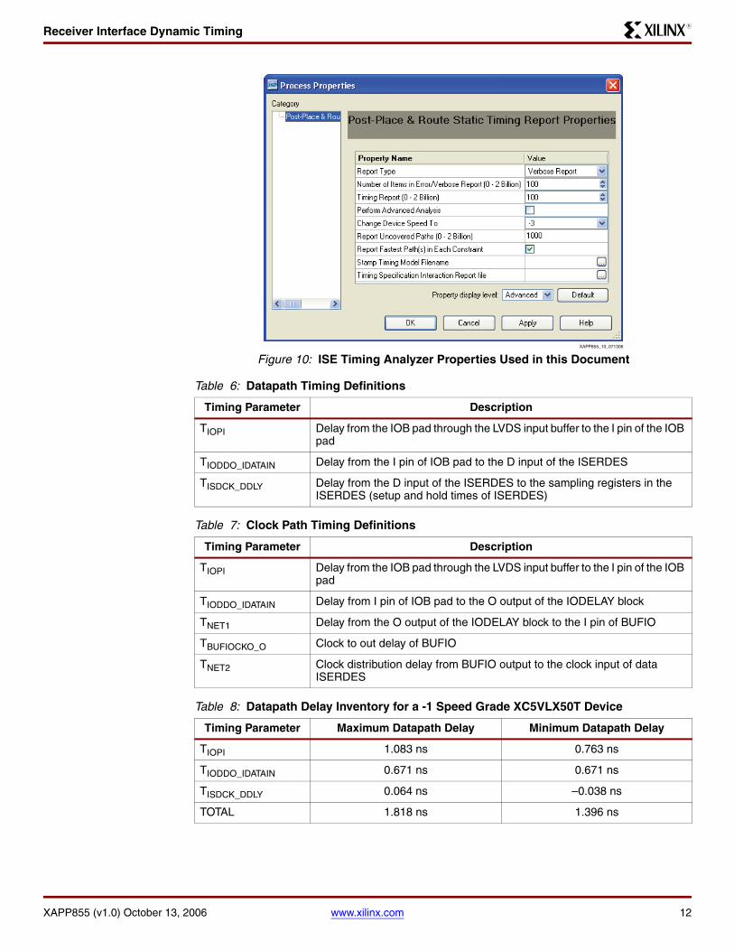
Receiver Interface Dynamic Timing
XAPP855 (v10) October 13 2006 wwwxilinxcom 12
R
Figure 10 ISE Timing Analyzer Properties Used in this Document
Table 6 Datapath Timing Definitions
Timing Parameter Description
TIOPI Delay from the IOB pad through the LVDS input buffer to the I pin of the IOB pad
TIODDO_IDATAIN Delay from the I pin of IOB pad to the D input of the ISERDES
TISDCK_DDLY Delay from the D input of the ISERDES to the sampling registers in the ISERDES (setup and hold times of ISERDES)
Table 7 Clock Path Timing Definitions
Timing Parameter Description
TIOPI Delay from the IOB pad through the LVDS input buffer to the I pin of the IOB pad
TIODDO_IDATAIN Delay from I pin of IOB pad to the O output of the IODELAY block
TNET1 Delay from the O output of the IODELAY block to the I pin of BUFIO
TBUFIOCKO_O Clock to out delay of BUFIO
TNET2 Clock distribution delay from BUFIO output to the clock input of data ISERDES
Table 8 Datapath Delay Inventory for a -1 Speed Grade XC5VLX50T Device
Timing Parameter Maximum Datapath Delay Minimum Datapath Delay
TIOPI 1083 ns 0763 ns
TIODDO_IDATAIN 0671 ns 0671 ns
TISDCK_DDLY 0064 ns ndash0038 ns
TOTAL 1818 ns 1396 ns
XAPP855_10_071306
Receiver Interface Dynamic Timing
XAPP855 (v10) October 13 2006 wwwxilinxcom 13
R
According to the inherent timing prediction the data is going to arrive before the clock by an amount determined by Equation 1 and Equation 2 Equation 1 calculates that data arrives before the clock by at least 1076 ns in a -1 device Equation 2 calculates that data arrives before the clock by at most 2213 ns Equation 3 shows a timing window that covers all -1 devices under all conditions This timing window describes the inherent timing of the data and clock paths Assuming skew-matched PCB traces for all sixteen channels then it can be assumed that all 16 channels in the receiver have roughly the same timing window
Equation 1
Equation 2
Equation 3
Figure 11 shows the timing windows for all speed grades of an XC5VLX50T device as well as a hardware measurement of the inherent timing relationship (to validate the calculations) The hardware measurement shows the DDR interface data arriving 1425 ns before the clock which by inspection places the device in all three speed grade ranges (the device used for the hardware measurement is a -2 device)
Table 9 Clock Path Delay Inventory for a -1 Speed Grade XC5VLX50T Device
Timing Parameter Maximum Clock Path Delay Minimum Clock Path Delay
TIOPI 1150 ns 0820 ns
TIODDO_IDATAIN 0671 ns 0671 ns
TNET1 0254 ns 0190 ns
TBUFIOCKO_O 1130 ns 0894 ns
TNET2 0404 ns 0319 ns
TOTAL 3609 ns 2894 ns
Setup Time Max Data Delay Min Clock Delay 1818 2894ndash 1076 nsndash==ndash=
Hold Time Max Clock Delay Min Data Delay 3609 1396ndash 2213 ns==ndash=
Timing Window 2213 1076ndash 1137 ns==
Figure 11 Timing Windows Show Uncertainty in ClockData Relationship as Calculated by Timing Analyzer
400 Mbs Data (T = 25 ns)
1425 ns Hardware MeasurementData Arrives
x855_11_091806
-11076ns 2213 ns
-21043 ns 2039 ns
-30989 ns 1878 ns
Receiver Interface Dynamic Timing
XAPP855 (v10) October 13 2006 wwwxilinxcom 14
R
Dynamic Timing and BIT_ALIGN_MACHINE
In ldquoInherent Timingrdquo page 11 the inherent timing of the interface was calculated for all speed grades and validated with a hardware measurement In that case the inherent timing was sufficient because the data rate is only 400 Mbs (Figure 11 page 13) What happens when the data rate is increased such that the hold edge of the data window begins to shrink (Figure 12)
At 600 Mbs the inherent timing relationship is no longer adequate to meet timing because there are cases when the sampling clock edge is in the middle of the data transition As the data rates increase to 800 and 1000 Mbs the clock actually captures the data arriving one bit time later For designs that are sensitive to word alignment this is unacceptable
The solution to the suboptimal inherent timing is dynamic timing The BIT_ALIGN_MACHINE module in the receiver performs two functions of dynamic timing
bull Bit Alignment Position the sampling edge of the clock at the center of the data eye by adding delay to the datapaths
bull Word Alignment Ensure that the parallel data bits are in the correct order at the output of the ISERDES by using the bitslip function in the ISERDES
The steps of the bit-alignment procedure are shown in Figure 13 page 15 Each step of the algorithm can either add or subtract delay from the datapath All 16 channels are taken through this procedure independently This procedure measures one full data eye (in terms of 75 ps delay taps) and then returns to the center of the data eye Steps 1 and 2 are dedicated to moving through the partial eye of the initial timing while steps 3 and 4 are dedicated to measuring a full eye Step 5 is dedicated to positioning the clock edge at the center of the data eye
Figure 12 Inherent Timing Windows Shown in Relation to Multiple Data Rates
400 Mbs Data (T = 25 ns)
600 Mbs Data (T = 167 ns)
800 Mbs Data (T = 127 ns)
1000 Mbs Data (T = 10 ns)
-11076ns 2213 ns
-21043 ns 2039 ns
-30989 ns
1425 ns
1878 ns
Hardware MeasurementData Arrives
x855_12_091806
Receiver Interface Dynamic Timing
XAPP855 (v10) October 13 2006 wwwxilinxcom 15
R
Jitter is represented in Figure 13 as multiple transition lines Accounting for jitter is a crucial part of the algorithm In step 2 the first data transition is found If there is no jitter then the eye measurement can begin instantly after finding the transition However when jitter is considered the algorithm must find the first transition move through the transition and then begin looking for the second transition If the algorithm does not move through the first transition intelligently it runs the risk of falsely detecting the second transition
Once bit alignment is complete the order of the data bits can be adjusted to achieve word alignment The bit-alignment procedure ensures that data is being sampled correctly but the order of the data can be a few bits off from where the receiver expects it to be To correct this the bitslip feature of the ISERDES is used to slip bit times until the proper alignment is found For this feature to be useful a training pattern must be generated by the transmitter (as discussed in ldquoDDR Transmitterrdquo page 3) that the receiver can use to determine the proper word alignment In this reference design the training pattern is 00101100 (0x2C) This pattern is mostly arbitrary as many other patterns work just as well This pattern was chosen because a training pattern should behave electrically as much like real data as possible such that the center of the training eye is the center of the data eye Since real data contains strings of consecutive ones and zeros it is best for the training pattern to do the same For that reason a 0x2C pattern is better than an 0xAA pattern because it contains run lengths of 1 2 3 and 4 bit times
Table 10 page 16 shows the word-alignment process in the case where bit alignment completes with the data outputs set to 0x58 Since 0x58 is not the training pattern the receiver is looking for bitslip is asserted until 0x2C is found This reference design uses a 18 deserialization so there are only eight possible configurations of the parallel data outputs If bitslip is asserted infinitely the same eight configurations will repeat Bitslip in DDR mode is somewhat irregular because it does not simply rotate by one bit on every bitslip cycle This effect is inconsequential to the word-alignment procedure (see the Virtex-5 User Guide for more details)
Figure 13 Dynamic Bit-Alignment Procedure in BIT_ALIGN_MACHINE
Data 0
Data Arrives Before Clock
Data 1
x855_13_091806
Data 0 Data 1
Data 0 Data 1
Data 0 Data 1
Data 0 Data 1
Sampling Clock (Fixed Delay)
Return to Center of Eye
End Measuring Eye
Begin Measuring Eye
Find 1st Transition
Initial Timing1
2
3
4
5
Receiver Interface Dynamic Timing
XAPP855 (v10) October 13 2006 wwwxilinxcom 16
R
The FSM in the BIT_ALIGN_MACHINE module used to implement both bit and word alignment is shown in Figure 14 page 17 The FSM is divided into five sections loosely described as finding the first transition getting through the first transition finding the second transition returning to the center of the eye and word alignment
To get through the first transition effectively for all possible types of jitter two methods are used The first method pertains to random jitter If there is a lot of random jitter at the sampling point then the samples generated are not stable The algorithm detects this instability by comparing current samples to older samples and therefore knows where the transition begins and ends But what if the jitter is extremely deterministic The transition then has discreet crossing points such that within the transition there is very stable but incorrect data In this case the algorithm does not sense any instability and falsely concludes that the sampling point is not in the transition To address this case apart from evaluating stability the algorithm also evaluates the correctness of the data content by using the bitslip feature in the middle of the transition For example if the algorithm determines that the sampled data is stable it then asserts bitslip to look for the correct data If 0x2c is found within eight assertions of bitslip then the sampling point is not in the transition But if 0x2c is not found then the algorithm increments the data delay and repeats the transition test again
Table 10 Word Alignment in the DDR Receiver
Bitslip Cycle Data Value (Hex) Data Value (Bin) Description of Bitslip operation
1 58 0101 1000 ndash
2 0B 0000 1011 Rotate 3 bits to right
3 16 0001 0110 Rotate 1 bit to left
4 C2 1100 0010 Rotate 3 bits to right
5 85 1000 0101 Rotate 1 bit to left
6 B0 1011 0000 Rotate 3 bits to right
7 61 0110 0001 Rotate 1 bit to left
8 2C 0010 1100 Rotate 3 bits to right
Receiver Interface Dynamic Timing
XAPP855 (v10) October 13 2006 wwwxilinxcom 17
R
Figure 14 FSM in the BIT_ALIGN_MACHINE Module
TRANSITION_CHECK (01000)
First TransitionNot Detected
First TransitionNot Detected
First TransitionDetected
First TransitionDetected
Past the FirstTransition
Second TransitionNot Detected
Second TransitionDetected
Decrement DelayAgain
Bit AlignmentComplete
Still Samplingin Transition
INC_ONCE (01111)
SEARCH_PAT (01101)
IDLE (01100)
IDLE (10000)
RECHECK_TRANS (00010)
ONE_BITSLIP (00110)
INC_ONCE (01011)
WAIT_8_CYCLES (00100)
COUNT_1 (01110)
INC_ONCE (01001)
WAIT_8_CYCLES (00011)
IDLE (10010)
TRAINING_DONE (00111)
FIRST_SAMPLE (00001)
RESET (00000)
DEC_TO_HALF (01010)
WORD_ALIGN (00101)
X855_14_082806
Routine to Avoid False Detection of Second Transition
=CHECK_PATTERN
Receiver Interface Dynamic Timing
XAPP855 (v10) October 13 2006 wwwxilinxcom 18
R
Interface Timing Budget
In addition to sampling the data as closely as possible to the center of the data eye the actual size of the data eye is important By accurately predicting the size of the data eye in the receiver the overall performance ceiling of the interface can be inferred The ideal data eye width is the period of the data rate (for example TBit_Period = 100 ns for 1000 Mbs) Both the transmitter and receiver circuits have sources of error that subtract from the ideal data eye The equation for the eye width at the output of the transmitter is shown in Equation 4 TJITTER is the peak-to-peak jitter of the clock source driving the transmitter data bus and forwarded clock TDCD is the maximum duty cycle distortion of the clock tree driving the data bus and forwarded clock Skew is not considered in the transmitter or receiver because the receiver calibrates out skew between channels by performing alignment on each channel individually
Equation 4
Equation 5 calculates the width of the data eye at the receiver flip-flops Ideally the eye width at the receiver is the same as the eye width at the output of the transmitter but there are sources of error in the transmission medium and receiver circuitry Duty cycle distortion must be considered again on the receiver clock tree TSAMP_BUFIO is the receiver sampling error due to drift caused by voltage and temperature variations TIDELAYPAT_JIT is the amount of pattern dependent jitter that is accumulated in each tap of the IDELAY chain For a clock pattern TIDELAYPAT_JIT is 0 pstap peak to peak For a data pattern with long and short run lengths of zeroes and ones (simulated by PRBS23) TIDELAYPAT_JIT is a finite value that must be considered in the timing budget
Equation 5
TBOARD_JITTER includes jitter induced by receiver input capacitance and the parasitics of the physical data path on the PCB TBOARD_JITTER must be determined by simulation as it varies as a function of frequency and for receivers of different types and vendors On the ML550 with a -2 speed-grade Virtex-5 device the TBOARD_JITTER is measured at roughly 200 ps at 900 Mbs (assuming data content equivalent to PRBS23) TQUANTIZATION_ERR or quantization error is caused by the granularity of the IDELAY tap chain Working with 75 ps increments it is not possible to utilize the entire data eye since inevitably some valid eye width is lost between two taps The value for this loss is 75 ps As long as the receiver eye width calculated using Equation 5 is greater than or equal to 0 the interface operates correctly over process voltage and temperature
For example Equation 6 and Equation 7 show the timing budget calculation for the DDR interface running at 900 Mbs in a -2 speed grade device on an ML550 evaluation board Refer to the data sheet for the most current values The TX interface is looped back to the RX interface on the same Virtex-5 FPGA as shown in Equation 2
Equation 6
Equation 7
Changes in voltage and temperature cause the data channels of the interface to drift relative to the clock If the DDR interface were to transfer user data for a long period of time over all specified conditions of temperature and voltage Equation 7 states that there would be at least 107 ps (one or two IDELAY taps) of data window remaining valid during all fluctuations of temperature and voltage Compare this calculation to the measurements in Table 12 page 21 Case 900 Mbs There are four taps that are error free under all conditions In ldquoAppendixrdquo there are three -2 devices tested at 900 Mbs and each has 4 4 and 3 taps respectively that are error free under all conditions
DATA_EYE_WIDTH_TX TBIT_PERIOD TJITTERndash TDCD_BUFIOndash=
DATA_EYE_WIDTH_RX DATA_EYE_WIDTH_TX
TBOARD_JITTER
ndash
TSAMP_BUFIOndash TDCD_BUFIOndash
TIDELAYPAT_JIT IDELAY taps in datapathtimes[ ]ndash
TQUANTIZATION_ERRndash
=
DATA_EYE_WIDTH_TX 1111 ps 25 psndash 100 psndash 986 ps= =
DATA_EYE_WIDTH_RX986 ps 200 psndash 400 psndash 100 psndash 8 ps 13 tapstimes[ ] 75 ps 107 ps=ndashndash
=
Interface Characterization
XAPP855 (v10) October 13 2006 wwwxilinxcom 19
R
At a given temperature and voltage setting the data valid window is much larger because there is no drift when temperature and voltage are constant The size of the data valid window under constant conditions is 107 ps + TSAMP_BUFIO which in this case is at least 507 ps (six or seven IDELAY taps) Compare this calculation to the measurements of any single condition in Table 12 Case 900 Mbs In the worst case (ndash5 supply) there are 7 taps that are error free
Equation 8 and Equation 9 show the same timing budget calculation for the DDR interface running at 10 Gbs in a -2 speed grade device on an ML550 Evaluation Board
Equation 8
Equation 9
Equation 9 predicts that no data window remains valid during all specified fluctuations of temperature and voltage (compare to Table 12 Case 1000 Mbs) In ldquoAppendixrdquo there are three -2 devices tested at 1000 Mbs and each has 1 3 and 1 taps respectively that are error free under all conditions This data rate and device combination are very marginal cases
To operate at 10 Gbs the DDR interface requires additional circuitry to track out voltage-temperature variations in real-time (see XAPP860 16-channel DDR LVDS Interface with Real-time Window Monitoring for a DDR Interface with real-time window monitoring) If the voltage-temperature variations are removed from the picture the predicted data valid window is ndash120 ps + TSAMP_BUFIO which in this case is at least 280 ps (3 or 4 taps) Compare this calculation to the measurements of any single condition in Table 18 page 34 There are at least four error-free taps in all conditions
Interface Characterization
By following the procedure illustrated in Figure 13 page 15 the bit-alignment algorithm should never insert more than approximately 15 bit times of delay on the data channels The fewest number of delay taps should be used in the datapath because they produce a finite amount of degradation (TIDELAYPAT_JIT) The worst-case initial timing for the algorithm occurs when the clock samples just before the data transitions as in the 600 Mbs case in Figure 12 page 14 The algorithm must move all the way through the first eye to find the first transition (1 bit time) and then move halfway into the next eye to center the sampling point (05 bit time) This process produces a worst-case total delay insertion of 15 bit times
The actual performance of the bit-alignment algorithm is characterized as a function of data rate in Figure 15 page 20 For all data rates the expectation is that the tap settings of all 16 channels in the DDR receiver do not exceed approximately 15 bit times of delay Both the maximum and minimum tap setting of all 16 channels is recorded for each data rate This graph only shows the data for a single device Comparing the 15 bit time mask to the actual settings it is clear that the algorithm remains within the 15 bit time limit At 13 Gbs the tap setting actually exceeds the mask by one tap (a negligible violation)
DATA_EYE_WIDTH_TX 1000 ps 25 psndash 100 psndash 875 ps= =
DATA_EYE_WIDTH_RX 875 ps 300 psndash400 ps 100 psndash
ndash8 ps 15 tapstimes[ ] 75 ps 120 psndash=ndashndash
=
Interface Characterization
XAPP855 (v10) October 13 2006 wwwxilinxcom 20
R
The maximum and minimum tap settings in Figure 15 generally stay within 3 to 4 taps of each other except in the case of 640 Mbs and 1300 Mbs data rates These data rates are seams in the inherent timing At data rates below 640 Mbs the tap settings are in the range of 30 taps and at data rates above 640 Mbs the tap settings are in the range of 12 taps Referring back to Figure 12 page 14 it is clear why this seam occurs As the data rate increases past 600 Mbs the initial sampling point of the inherent timing moves into a different data eye creating a different starting point for the algorithm At 640 Mbs some of the 16 channels start in one eye while other channels start in the other eye Fortunately this is not an issue because the single bit time of difference between the channels is resolved using bitslip
Referring back to Figure 8 page 9 the clock channel goes through an IDELAY block with a default value of 0 Once the data rate is chosen for a given design this initial IDELAY value can be changed to a non-zero value to achieve more favorable inherent timing For example a design running at 620 Mbs can use 30 IDELAY taps on the delay channels each contributing a certain amount of jitter to the timing budget calculation By setting the initial clock delay to 5 taps the inherent timing moves across the seam shown in the 600 Mbs range of Figure 15 causing the data channels to only use about 12 IDELAY taps Only spectrally rich data patterns accumulate jitter in the IDELAY tap chain so the clock IDELAY can be set to any value without diminishing the timing budget This optimization is entirely optional and can be done once the design is running in hardware
The DDR receiver is designed to remove skew between channels by aligning each channel individually The ML550 board on which this reference design is characterized is designed to have minimal skew between channels However there is clearly a finite amount of skew between channels due to clock skew in the TX and RX BUFIO networks package skew and trace length tolerance on the ML550 board Table 11 page 21 shows how the bit-alignment algorithm sets the delay for each channel differently to compensate for skew between channels The table captures the range of settings among the 16 channels at specific data rates for a -2 device If there were additional skew among the 16 channels then the tap setting range would be larger to compensate for it The algorithm is designed such that skew between channels should not diminish the performance of the interface The range of tap settings differs for different devices and speed grades but the magnitude should be approximately the same
Figure 15 Bit-Alignment Algorithm Performance
60
50
40
30
20
10
0200 400 600 800 1000 1200 1400 1600
Data Rate (Mbs)
Del
ay T
ap U
tiliz
atio
n HW Measurement (Min)HW Measurement (Max)15 Bit Time Mask
X855_15_072406
Interface Characterization
XAPP855 (v10) October 13 2006 wwwxilinxcom 21
R
Since the receiver alignment logic only runs once immediately after reset the resulting dynamic timing must be adequate to ensure error-free operation over the specified voltage and temperature variations that can occur over time The data-valid window at the receiver input must be wide enough to withstand these variations (receiver drift) Table 12 page 21 shows the data-valid window at the ISERDES registers in the DDR receiver The eyes shown are collective eyes of all 16 channels The BERT testbench configuration loops back the DDR transmitter to the DDR receiver Using pattern generators and error detectors programmed to send and receive a pseudorandom bit sequence (PRBS23) the width of the data-valid window is evaluated using pseudorandom data that closely resembles real user data
Table 11 Tap Setting Range For Various Data Rates Measured on a -2 Device
Data Rate (Mbs) Tap Setting Range Compensated Skew
500 31ndash34 4 taps
600 28ndash30 3 taps
700 10ndash12 3 taps
800 11ndash13 3 taps
900 11ndash13 3 taps
1000 13ndash15 3 taps
1100 13ndash15 3 taps
1200 14ndash15 2 taps
Table 12 Measurement of Receiver Drift under Extreme Conditions for Multiple Data Rates
ConditionIODELAY Taps (1)
ndash8 ndash7 ndash6 ndash5 ndash4 ndash3 ndash2 ndash1 0 +1 +2 +3 +4 +5 +6 +7 +8
Case 800 Mbs
25degC Nom Supplies F F F P P P P P C P P P P P F F F
0degC Nom Supplies F F F P P P P P P P P P P P F F F
85degC Nom Supplies F F F P P P P P P P P P P P F F F
25degC +5 Supplies F P P P P P P P P P P P F F F F F
0degC +5 Supplies F P P P P P P P P P P P F F F F F
85degC +5 Supplies F P P P P P P P P P P P F F F F F
25degC ndash5 Supplies F F F F F F P P P P P P P P P F F
0degC ndash5 Supplies F F F F F F P P P P P P P P P P F
85degC ndash5 Supplies F F F F F P P P P P P P P P P F F
CONCLUSION Error free under all conditions when calibrated under nominal conditions to position C
Interface Characterization
XAPP855 (v10) October 13 2006 wwwxilinxcom 22
R
Case 900 Mbs
25degC Nom Supplies F F F F P P P P C P P P P F F F F
0degC Nom Supplies F F F F P P P P P P P P P F F F F
85degC Nom Supplies F F F F P P P P P P P P F F F F F
25degC +5 Supplies F F P P P P P P P P P F F F F F F
0degC +5 Supplies F F P P P P P P P P P F F F F F F
85degC +5 Supplies F F P P P P P P P P P F F F F F F
25degC ndash5 Supplies F F F F F F F P P P P P P P P F F
0degC ndash5 Supplies F F F F F F F P P P P P P P P F F
85degC ndash5 Supplies F F F F F F F P P P P P P P F F F
CONCLUSION Error free under all conditions when calibrated under nominal conditions to position C
Case 1000 Mbs
25degC Nom Supplies F F F F F P P P C P P P F F F F F
0degC Nom Supplies F F F F F P P P P P P P F F F F F
85degC Nom Supplies F F F F F P P P P P P P F F F F F
25degC +5 Supplies F F F P P P P P P P F F F F F F F
0degC +5 Supplies F F F P P P P P P P F F F F F F F
85degC +5 Supplies F F F P P P P P P P P F F F F F F
25degC ndash5 Supplies F F F F F F F F P P P P P P F F F
0degC ndash5 Supplies F F F F F F F F P P P P P P F F F
85degC ndash5 Supplies F F F F F F F F P P P P P P F F F
CONCLUSION Error free under all conditions when calibrated under nominal conditions to position C
Case 1100 Mbs
25degC Nom Supplies F F F F F P P P C P F F F F F F F
0degC Nom Supplies F F F F F P P P P P F F F F F F F
85degC Nom Supplies F F F F F P P P P P F F F F F F F
25degC +5 Supplies F F F P P P P P P F F F F F F F F
0degC +5 Supplies F F F P P P P P P F F F F F F F F
85degC +5 Supplies F F F P P P P P P F F F F F F F F
25degC ndash5 Supplies F F F F F F F F P P P P F F F F F
0degC ndash5 Supplies F F F F F F F F P P P P F F F F F
85degC ndash5 Supplies F F F F F F F F P P P P F F F F F
CONCLUSION Error free under all conditions when calibrated under nominal conditions to position C
Table 12 Measurement of Receiver Drift under Extreme Conditions for Multiple Data Rates (Continued)
ConditionIODELAY Taps (1)
ndash8 ndash7 ndash6 ndash5 ndash4 ndash3 ndash2 ndash1 0 +1 +2 +3 +4 +5 +6 +7 +8
Interface Characterization
XAPP855 (v10) October 13 2006 wwwxilinxcom 23
R
In all test cases shown in Table 12 page 21 the bit-align machine accurately places the sampling point in the center of the data eye (indicated by the C in each test case) In the 1100 Mbs case the bit-align machine places the sampling point slightly off center This slight inaccuracy occurs when the center of a real data pattern diverges from the center of the training pattern The electrical behavior of different data patterns is discussed below
After the dynamic timing is established for a given test case under nominal conditions the device is subjected to extremes of temperature and voltage to stress the receiver timing At data rates of 1100 Mbs and below the dynamic timing established after reset under nominal conditions is sufficient to meet timing over all specified extreme conditions (the column with the C passes traffic error free under all conditions) At a data rate of 1200 Mbs the design operates correctly under nominal conditions but the data-valid window is not large enough to withstand the voltage variations For this particular transmission medium the 1200 Mbs case requires a real-time adjustment circuit that could track the center of the eye
The full datapath of the testbench consists of
TX rarr 5 FR-4 rarr SAMTEC QSE Conn rarr 12 Ribbon Cable rarr SAMTEC QSE Conn rarr 5 FR-4 rarr RX
For shorter transmission media higher performance can be achieved in accordance with the section ldquoInterface Timing Budgetrdquo page 18 Interface performance is not solely a question of the LVDS driver performance specification but rather a question of adequate timing margin to withstand production and environmental variations From Table 12 the total amount of variation experienced over temperature and voltage is roughly 375 ps (5 taps at 75 ps per tap) This number should be comparable to the specification for receiver sampling error (TSAMP_BUFIO) shown in the Virtex-5 Data Sheet
Case 1200 Mbs
25degC Nom Supplies F F F F F F P P C P F F F F F F F
0degC Nom Supplies F F F F F F P P P P F F F F F F F
85degC Nom Supplies F F F F F F P P P F F F F F F F F
25degC +5 Supplies F F F F P P P P F F F F F F F F F
0degC +5 Supplies F F F P P P P P F F F F F F F F F
85degC +5 Supplies F F F F P P P P F F F F F F F F F
25degC ndash5 Supplies F F F F F F F F F P P P F F F F F
0degC ndash5 Supplies F F F F F F F F F P P P F F F F F
85degC ndash5 Supplies F F F F F F F F F P P F F F F F F
CONCLUSION Errors caused by plusmn5 variations in supply voltages
Notes 1 Where 0 is the reference tap determined by the bit-align machine under nominal conditions at 25degC2 P = Error-free transmission F = Error in transmission C = IODELAY tap position selected by bit-align machine under nominal conditions at 25degC3 Device under test is -2 speed grade
Table 12 Measurement of Receiver Drift under Extreme Conditions for Multiple Data Rates (Continued)
ConditionIODELAY Taps (1)
ndash8 ndash7 ndash6 ndash5 ndash4 ndash3 ndash2 ndash1 0 +1 +2 +3 +4 +5 +6 +7 +8
Interface Characterization
XAPP855 (v10) October 13 2006 wwwxilinxcom 24
R
Pattern Dependence of Receiver Performance
Different types of data patterns have different electrical signatures (rise and fall times jitter eye symmetry etc) A pattern with very narrow spectral content (such as a clock pattern) moves very favorably through the link because the receiver frequency response has little effect on the signal integrity However a pattern with wide spectral content (such as real data and pseudorandom patterns) stresses the links frequency response If the frequency response is not flat across the entire spectrum of the data content then the signal integrity is degraded as a result The amount of degradation measured is shown in Table 13 page 25 The DDR transmitter is looped back to the DDR receiver and different patterns are programmed to traverse the link Performance is assessed by evaluating the integrity of those patterns in the receiver
PRBS7 is a pseudorandom data pattern with a maximum run length of seven consecutive zeroes or ones PRBS15 is defined as having a maximum run length of fifteen consecutive zeroes or ones These limitations on run lengths limit the spectral content of the pattern A PRBS15 pattern has greater spectral content than a PRBS7 pattern and therefore is a more strenuous test for the link PRBS29 is the most strenuous test in Table 13 A clock pattern is effectively a PRBS1
As predicted Table 13 shows that there is more degradation for data patterns with more spectral content At 1000 Mbs and below the data eye closure is symmetrical Symmetrical eye closure is desired because it does not change the center of the eye as determined by the bit-alignment algorithm Above 1000 Mbs the eye closure becomes more asymmetrical causing the center of the data eye to diverge from the calibrated center (by only 1 tap)
In every data rate shown in Table 13 all significant pattern-dependent degradation is caused between PRBS1 (clock pat) and PRBS15 Between PRBS15 and PRBS29 there is no additional degradation recorded in any of the measurements
Interface Characterization
XAPP855 (v10) October 13 2006 wwwxilinxcom 25
R
Table 13 Link Performance for Various Types of Data Measured on a -2 Device
PatternIODELAY Taps (1)
ndash8 ndash7 ndash6 ndash5 ndash4 ndash3 ndash2 ndash1 0 +1 +2 +3 +4 +5 +6 +7 +8 +9
Case 600 Mbs
Clock Pat (0101) P P P P P P P P C P P P P P P P P P
Training Pat (0x2C) P P P P P P P P C P P P P P P P P F
PRBS7 P P P P P P P P C P P P P P P P P F
PRBS15 F P P P P P P P C P P P P P P P F F
PRBS23 F P P P P P P P C P P P P P P P F F
PRBS29 F P P P P P P P C P P P P P P P F F
Case 800 Mbs
Clock Pat (0101) F F P P P P P P C P P P P P P F F F
Training Pat (0x2C) F F P P P P P P C P P P P P P F F F
PRBS7 F F P P P P P P C P P P P P F F F F
PRBS15 F F F P P P P P C P P P P P F F F F
PRBS23 F F F P P P P P C P P P P P F F F F
PRBS29 F F F P P P P P C P P P P P F F F F
Case 1000 Mbs
Clock Pat (0101) F F F P P P P P C P P P P P F F F F
Training Pat (0x2C) F F F P P P P P C P P P P F F F F F
PRBS7 F F F F P P P P C P P P F F F F F F
PRBS15 F F F F F P P P C P P P F F F F F F
PRBS23 F F F F F P P P C P P P F F F F F F
PRBS29 F F F F F P P P C P P P F F F F F F
Case 1200 Mbs
Clock Pat (0101) F F F F P P P P C P P P P F F F F F
Training Pat (0x2C) F F F F P P P P C P P P F F F F F F
PRBS7 F F F F F P P P C P F F F F F F F F
PRBS15 F F F F F F P P C F F F F F F F F F
PRBS23 F F F F F F P P C F F F F F F F F F
PRBS29 F F F F F F P P C F F F F F F F F F
Case 1400 Mbs
Clock Pat (0101) F F F F F F P P C P P P F F F F F F
Training Pat (0x2C) F F F F F P P P C P P F F F F F F F
PRBS7 F F F F F F F P C P F F F F F F F F
PRBS15 F F F F F F F P C F F F F F F F F F
PRBS23 F F F F F F F P C F F F F F F F F F
PRBS29 F F F F F F F P C F F F F F F F F F
Notes 1 Where 0 is the reference tap determined by the bit-align machine under nominal conditions at 25degC2 P = Error-free transmission F = Error in transmission C = IODELAY tap position selected by bit-align machine under nominal conditions at 25degC
Resetting the Interface
XAPP855 (v10) October 13 2006 wwwxilinxcom 26
R
Resetting the Interface
Several dependencies determine the order in which circuits should be reset in the interface The receiver cannot begin the alignment algorithm if the transmitter is not sending the training pattern The transmitter must be reset before the receiver and time must be allowed for the training pattern to propagate across the link before the receiver comes out of reset The receiver also cannot begin the alignment algorithm until IDELAYCTRL has recovered from reset which could takes hundreds of cycles The recommended reset timing for the interface is shown in Figure 16 This reset timing is implemented in the BERT testbench for this interface
The TX reset (RST_TX) is used to reset all TX circuitry and also IDELAYCTRL The IDELAYCTRL reset is asynchronous so driving it with RST_TX is acceptable The minimum pulse width of IDELAYCTRL reset is 50 ns (TIDELAYCTRL_RPW) For that reason resets are held High for 16 clock cycles The RX reset (RST_RX) is used to reset all RX circuitry and is asserted when the IDELAYCTRL READY flag goes High indicating that the IODELAY blocks are calibrated
The timing of the READY flag in Figure 16 is a potential hazard Most likely it is High during a TX reset because it takes many cycles for IDELAYCTRL to deassert the READY flag It is easy to make the mistake of resetting the receiver too early To avoid this hazard the RX reset should be asserted only after seeing a deassertion and reassertion of the READY flag
Conclusion Based on the design and characterization described in this document the 16-Channel DDR reference design operates to the performance targets in Table 14 under all conditions of process voltage and temperature However to meet these targets over voltage and temperature the timing budget must be guaranteed according to the analysis in ldquoInterface Timing Budgetrdquo See ldquoAppendixrdquo page 27 for further justification of the maximum performance recommendations in Table 14
Figure 16 Recommended Interface Reset Timing
RST_TX
IDELAYCTRLREADY
RST_RX
16 Cycles X855_16_072406
Table 14 Performance of 16-Channel DDR Interface
Speed Grade Maximum Performance
-1 800 Mbs
-2 900 Mbs
-3 10 Gbs(1)
Notes 1 To achieve higher performance (up to 125 Gbs) see 16-channel DDR LVDS Interface with Realtime
Window Monitoring for an example of a DDR interface with real-time window monitoring
Appendix
XAPP855 (v10) October 13 2006 wwwxilinxcom 27
R
Appendix Performance Characterization Data
Refer to ldquoInterface Characterizationrdquo page 19 for explanations about how to interpret the data in the ldquoAppendixrdquo These tables show collective data eyes for the entire interface over process voltage and temperature (PVT) Three devices from each speed grade were selected for this characterization
The calibrated center position of the eye (marked by the C in the tables below) varies slightly from channel to channel (due to small skews between channels) That range is referred to as center tap range Analysis of Table 16 page 28 through Table 20 page 40 shows that the center tap range for slow and fast parts differ significantly at the same data rate (because the BIT_ALIGN_MACHINE algorithm adjusts for differences in speed)
All data in the ldquoAppendixrdquo is collected using the BERT testbench shown in Figure 2 page 2 The data pattern is PRBS23 and the devicepackage is XC5VLX50T-FF1136 The transmission path for the cases shown in Table 16 through Table 20 is repeated for convenience
TX rarr 5 FR-4 rarr SAMTEC QSE Conn rarr 12 Ribbon Cable rarr SAMTEC QSE Conn rarr 5 FR-4 rarr RX
A summary of these characterization results is shown in Table 15 Each of the nine parts were tested at 800 900 1000 1100 and 1200 Mbs When the interface is error free on all channels under all extreme conditions of temperature and voltage the particular test case is designated by a P A test case is marked FAIL when the interface suffered errors on any channel under any particular condition of voltage and temperature
Table 15 Summary of Interface Characterization Results
Device (SN) Speed Grade 800 Mbs 900 Mbs 1000Mbs 1100 Mbs 1200 Mbs
2194 -1 P P P FAIL FAIL
2219 -1 P FAIL FAIL FAIL FAIL
2199 -1 P P FAIL FAIL FAIL
001 -2 P P FAIL P FAIL
002 -2 P P P P FAIL
003 -2 P P FAIL FAIL FAIL
004 -3 P P P P P
005 -3 P P P P P
006 -3 P P P P P
Appendix
XAPP855 (v10) October 13 2006 wwwxilinxcom 28
R
Table 16 Measurement of Receiver Drift under Extreme Conditions at 800 Mbs
ConditionIODELAY Taps (1)
ndash8 ndash7 ndash6 ndash5 ndash4 ndash3 ndash2 ndash1 0 +1 +2 +3 +4 +5 +6 +7 +8
SN 2194 Speed Grade -1
25degC Nom Supplies F F F P P P P P C P P P P F F F F
0degC Nom Supplies F F F P P P P P P P P P P F F F F
85degC Nom Supplies F F F F P P P P P P P P P F F F F
25degC +5 Supplies F F P P P P P P P P P P F F F F F
0degC +5 Supplies F F P P P P P P P P P P F F F F F
85degC +5 Supplies F F P P P P P P P P P P F F F F F
25degC ndash5 Supplies F F F F F F P P P P P P P P P F F
0degC ndash5 Supplies F F F F F F P P P P P P P P P F F
85degC ndash5 Supplies F F F F F F P P P P P P P P P F F
Center Tap Range Taps 11ndash12
CONCLUSION Error free under all conditions when calibrated under nominal conditions to position C
SN 2219 Speed Grade -1
25degC Nom Supplies F F F P P P P P C P P P F F F F F
0degC Nom Supplies F F F P P P P P P P P P F F F F F
85degC Nom Supplies F F F P P P P P P P P P F F F F F
25degC +5 Supplies F P P P P P P P P P P F F F F F F
0degC +5 Supplies F P P P P P P P P P P F F F F F F
85degC +5 Supplies F P P P P P P P P P P F F F F F F
25degC ndash5 Supplies F F F F F F P P P P P P P P F F F
0degC ndash5 Supplies F F F F F F F P P P P P P P F F F
85degC ndash5 Supplies F F F F F F P P P P P P P P F F F
Center Tap Range Taps 13ndash16
CONCLUSION Error free under all conditions when calibrated under nominal conditions to position C
SN 2199 Speed Grade -1
25degC Nom Supplies F F F P P P P P C P P P P F F F F
0degC Nom Supplies F F F P P P P P P P P P P F F F F
85degC Nom Supplies F F F P P P P P P P P P P F F F F
25degC +5 Supplies F P P P P P P P P P P P F F F F F
0degC +5 Supplies F P P P P P P P P P P P F F F F F
85degC +5 Supplies F P P P P P P P P P P P F F F F F
25degC ndash5 Supplies F F F F F F P P P P P P P P P F F
0degC ndash5 Supplies F F F F F F P P P P P P P P P F F
85degC ndash5 Supplies F F F F F F P P P P P P P P P F F
Center Tap Range Taps 10ndash12
CONCLUSION Error free under all conditions when calibrated under nominal conditions to position C
Appendix
XAPP855 (v10) October 13 2006 wwwxilinxcom 29
R
SN 001 Speed Grade -2
25degC Nom Supplies F F F P P P P P C P P P P F F F F
0degC Nom Supplies F F F P P P P P P P P P P F F F F
85degC Nom Supplies F F F P P P P P P P P P P F F F F
25degC +5 Supplies F P P P P P P P P P P P F F F F F
0degC +5 Supplies F P P P P P P P P P P F F F F F F
85degC +5 Supplies F P P P P P P P P P P P F F F F F
25degC ndash5 Supplies F F F F F P P P P P P P P P P F F
0degC ndash5 Supplies F F F F F P P P P P P P P P P F F
85degC ndash5 Supplies F F F F F P P P P P P P P P P F F
Center Tap Range Taps 10ndash12
CONCLUSION Error free under all conditions when calibrated under nominal conditions to position C
SN 002 Speed Grade -2
25degC Nom Supplies F F F P P P P P C P P P P F F F F
0degC Nom Supplies F F F P P P P P P P P P P F F F F
85degC Nom Supplies F F F P P P P P P P P P P F F F F
25degC +5 Supplies F P P P P P P P P P P P F F F F F
0degC +5 Supplies F P P P P P P P P P P P F F F F F
85degC +5 Supplies F F P P P P P P P P P P F F F F F
25degC ndash5 Supplies F F F F F P P P P P P P P P P F F
0degC ndash5 Supplies F F F F F P P P P P P P P P P F F
85degC ndash5 Supplies F F F F F P P P P P P P P P P F F
Center Tap Range Taps 10ndash12
CONCLUSION Error free under all conditions when calibrated under nominal conditions to position C
SN 003 Speed Grade -2
25degC Nom Supplies F F F P P P P P C P P P P F F F F
0degC Nom Supplies F F F P P P P P P P P P P F F F F
85degC Nom Supplies F F F P P P P P P P P P P F F F F
25degC +5 Supplies F P P P P P P P P P P P F F F F F
0degC +5 Supplies F P P P P P P P P P P F F F F F F
85degC +5 Supplies F P P P P P P P P P P P F F F F F
25degC ndash5 Supplies F F F F F F P P P P P P P P P F F
0degC ndash5 Supplies F F F F F F P P P P P P P P P F F
85degC ndash5 Supplies F F F F F F P P P P P P P P P F F
Center Tap Range Taps 11ndash13
CONCLUSION Error free under all conditions when calibrated under nominal conditions to position C
Table 16 Measurement of Receiver Drift under Extreme Conditions at 800 Mbs (Continued)
ConditionIODELAY Taps (1)
ndash8 ndash7 ndash6 ndash5 ndash4 ndash3 ndash2 ndash1 0 +1 +2 +3 +4 +5 +6 +7 +8
Appendix
XAPP855 (v10) October 13 2006 wwwxilinxcom 30
R
SN 004 Speed Grade -3
25degC Nom Supplies F F F P P P P P C P P P P F F F F
0degC Nom Supplies F F F P P P P P P P P P F F F F F
85degC Nom Supplies F F F P P P P P P P P P P F F F F
25degC +5 Supplies F P P P P P P P P P P P F F F F F
0degC +5 Supplies F P P P P P P P P P P P F F F F F
85degC +5 Supplies F F P P P P P P P P P P F F F F F
25degC ndash5 Supplies F F F F F P P P P P P P P P F F F
0degC ndash5 Supplies F F F F F P P P P P P P P P F F F
85degC ndash5 Supplies F F F F F P P P P P P P P P F F F
Center Tap Range Taps 8ndash9 23ndash24
CONCLUSION Error free under all conditions when calibrated under nominal conditions to position C
SN 005 Speed Grade -3
25degC Nom Supplies F F P P P P P P C P P P P F F F F
0degC Nom Supplies F F P P P P P P P P P P P F F F F
85degC Nom Supplies F F F P P P P P P P P P P P F F F
25degC +5 Supplies F P P P P P P P P P P P F F F F F
0degC +5 Supplies F P P P P P P P P P P P F F F F F
85degC +5 Supplies F P P P P P P P P P P P F F F F F
25degC ndash5 Supplies F F F F P P P P P P P P P P P F F
0degC ndash5 Supplies F F F F P P P P P P P P P P P F F
85degC ndash5 Supplies F F F F P P P P P P P P P P P F F
Center Tap Range Taps 9ndash10
CONCLUSION Error free under all conditions when calibrated under nominal conditions to position C
SN 006 Speed Grade -3
25degC Nom Supplies F F P P P P P P C P P P P F F F F
0degC Nom Supplies F F P P P P P P P P P P P F F F F
85degC Nom Supplies F F F P P P P P P P P P P F F F F
25degC +5 Supplies F P P P P P P P P P P P F F F F F
0degC +5 Supplies F P P P P P P P P P P P F F F F F
85degC +5 Supplies F F P P P P P P P P P P F F F F F
25degC ndash5 Supplies F F F P P P P P P P P P P P F F F
0degC ndash5 Supplies F F F P P P P P P P P P P P F F F
85degC ndash5 Supplies F F F F F P P P P P P P P P F F F
Center Tap Range Taps 8ndash9 23ndash24
CONCLUSION Error free under all conditions when calibrated under nominal conditions to position C
Notes 1 IODELAY taps where 0 is the reference tap determined by the bit align machine at nominal voltage and 25degC2 P = Error-free transmission F = Error in transmission C = IODELAY tap position selected by bit-align machine under nominal conditions at 25degC
Table 16 Measurement of Receiver Drift under Extreme Conditions at 800 Mbs (Continued)
ConditionIODELAY Taps (1)
ndash8 ndash7 ndash6 ndash5 ndash4 ndash3 ndash2 ndash1 0 +1 +2 +3 +4 +5 +6 +7 +8
Appendix
XAPP855 (v10) October 13 2006 wwwxilinxcom 31
R
Table 17 Measurement of Receiver Drift under Extreme Conditions at 900 Mbs
ConditionIODELAY Taps (1)
ndash8 ndash7 ndash6 ndash5 ndash4 ndash3 ndash2 ndash1 0 +1 +2 +3 +4 +5 +6 +7 +8
SN 2194 Speed Grade -1
25degC Nom Supplies F F F F F P P P C P P P F F F F F
0degC Nom Supplies F F F F F P P P P P P P F F F F F
85degC Nom Supplies F F F F F P P P P P P P P F F F F
25degC +5 Supplies F F F P P P P P P P P F F F F F F
0degC +5 Supplies F F F P P P P P P P P F F F F F F
85degC +5 Supplies F F F P P P P P P P P F F F F F F
25degC ndash5 Supplies F F F F F F F P P P P P P P F F F
0degC ndash5 Supplies F F F F F F F P P P P P P P F F F
85degC ndash5 Supplies F F F F F F F P P P P P P P F F F
Center Tap Range Taps 11ndash12
CONCLUSION Error free under all conditions when calibrated under nominal conditions to position C
SN 2219 Speed Grade -1
25degC Nom Supplies F F F F F P P P C P P P F F F F F
0degC Nom Supplies F F F F F P P P P P P P F F F F F
85degC Nom Supplies F F F F F P P P P P P P F F F F F
25degC +5 Supplies F F F P P P P P P P F F F F F F F
0degC +5 Supplies F F F P P P P P P P F F F F F F F
85degC +5 Supplies F F F P P P P P P P F F F F F F F
25degC ndash5 Supplies F F F F F F F F F P P P P P F F F
0degC ndash5 Supplies F F F F F F F F F P P P P P F F F
85degC ndash5 Supplies F F F F F F F F P P P P P P F F F
Center Tap Range Taps 12ndash15
CONCLUSION Errors caused by ndash5 variation in supply voltage
SN 2199 Speed Grade -1
25degC Nom Supplies F F F F F P P P C P P P F F F F F
0degC Nom Supplies F F F F F P P P P P P P F F F F F
85degC Nom Supplies F F F F F P P P P P P P F F F F F
25degC +5 Supplies F F F P P P P P P P P F F F F F F
0degC +5 Supplies F F F P P P P P P P P F F F F F F
85degC +5 Supplies F F F P P P P P P P P F F F F F F
25degC ndash5 Supplies F F F F F F F F P P P P P P F F F
0degC ndash5 Supplies F F F F F F F F P P P P P P F F F
85degC ndash5 Supplies F F F F F F F F P P P P P P F F F
Center Tap Range Taps 10ndash12
CONCLUSION Error free under all conditions when calibrated under nominal conditions to position C
Appendix
XAPP855 (v10) October 13 2006 wwwxilinxcom 32
R
SN 001 Speed Grade -2
25degC Nom Supplies F F F F P P P P C P P P P F F F F
0degC Nom Supplies F F F F P P P P P P P P P F F F F
85degC Nom Supplies F F F F F P P P P P P P P F F F F
25degC +5 Supplies F F P P P P P P P P P F F F F F F
0degC +5 Supplies F F P P P P P P P P P F F F F F F
85degC +5 Supplies F F F P P P P P P P P P F F F F F
25degC ndash5 Supplies F F F F F F F P P P P P P P F F F
0degC ndash5 Supplies F F F F F F F P P P P P P P F F F
85degC ndash5 Supplies F F F F F F F P P P P P P P F F F
Center Tap Range Taps 9ndash11
CONCLUSION Error free under all conditions when calibrated under nominal conditions to position C
SN 002 Speed Grade -2
25degC Nom Supplies F F F F P P P P C P P P P F F F F
0degC Nom Supplies F F F F P P P P P P P P F F F F F
85degC Nom Supplies F F F F F P P P P P P P P F F F F
25degC +5 Supplies F F F P P P P P P P P F F F F F F
0degC +5 Supplies F F F P P P P P P P P F F F F F F
85degC +5 Supplies F F F P P P P P P P P P F F F F F
25degC ndash5 Supplies F F F F F F F P P P P P P P F F F
0degC ndash5 Supplies F F F F F F F P P P P P P P F F F
85degC ndash5 Supplies F F F F F F F P P P P P P P F F F
Center Tap Range Taps 10ndash12
CONCLUSION Error free under all conditions when calibrated under nominal conditions to position C
SN 003 Speed Grade -2
25degC Nom Supplies F F F F F P P P C P P P P F F F F
0degC Nom Supplies F F F F F P P P P P P P P F F F F
85degC Nom Supplies F F F F F P P P P P P P P F F F F
25degC +5 Supplies F F P P P P P P P P P F F F F F F
0degC +5 Supplies F F P P P P P P P P P F F F F F F
85degC +5 Supplies F F F P P P P P P P P F F F F F F
25degC ndash5 Supplies F F F F F F F P P P P P P P F F F
0degC ndash5 Supplies F F F F F F F F P P P P P P F F F
85degC ndash5 Supplies F F F F F F F P P P P P P P F F F
Center Tap Range Taps 11ndash13
CONCLUSION Error free under all conditions when calibrated under nominal conditions to position C
Table 17 Measurement of Receiver Drift under Extreme Conditions at 900 Mbs (Continued)
ConditionIODELAY Taps (1)
ndash8 ndash7 ndash6 ndash5 ndash4 ndash3 ndash2 ndash1 0 +1 +2 +3 +4 +5 +6 +7 +8
Appendix
XAPP855 (v10) October 13 2006 wwwxilinxcom 33
R
SN 004 Speed Grade -3
25degC Nom Supplies F F F F P P P P C P P P P F F F F
0degC Nom Supplies F F F P P P P P P P P P P F F F F
85degC Nom Supplies F F F F P P P P P P P P P F F F F
25degC +5 Supplies F F F P P P P P P P P P F F F F F
0degC +5 Supplies F F F P P P P P P P P P F F F F F
85degC +5 Supplies F F F P P P P P P P P P F F F F F
25degC ndash5 Supplies F F F F F F P P P P P P P P F F F
0degC ndash5 Supplies F F F F F F P P P P P P P P F F F
85degC ndash5 Supplies F F F F F F P P P P P P P P F F F
Center Tap Range Taps 7ndash8
CONCLUSION Error free under all conditions when calibrated under nominal conditions to position C
SN 005 Speed Grade ndash3
25degC Nom Supplies F F F P P P P P C P P P P F F F F
0degC Nom Supplies F F F P P P P P P P P P P F F F F
85degC Nom Supplies F F F F P P P P P P P P P F F F F
25degC +5 Supplies F F P P P P P P P P P P F F F F F
0degC +5 Supplies F F P P P P P P P P P P F F F F F
85degC +5 Supplies F F F P P P P P P P P P F F F F F
25degC ndash5 Supplies F F F F F F P P P P P P P P F F F
0degC ndash5 Supplies F F F F F P P P P P P P P P F F F
85degC ndash5 Supplies F F F F F F P P P P P P P P F F F
Center Tap Range Taps 9ndash10
CONCLUSION Error free under all conditions when calibrated under nominal conditions to position C
SN 006 Speed Grade -3
25degC Nom Supplies F F F F P P P P C P P P P F F F F
0degC Nom Supplies F F F F P P P P P P P P P F F F F
85degC Nom Supplies F F F F P P P P P P P P P F F F F
25degC +5 Supplies F F P P P P P P P P P P F F F F F
0degC +5 Supplies F F P P P P P P P P P P F F F F F
85degC +5 Supplies F F F P P P P P P P P P F F F F F
25degC ndash5 Supplies F F F F F P P P P P P P P P F F F
0degC ndash5 Supplies F F F F F P P P P P P P P P F F F
85degC ndash5 Supplies F F F F F F P P P P P P P P F F F
Center Tap Range Taps 7ndash8
CONCLUSION Error free under all conditions when calibrated under nominal conditions to position C
Notes 1 IODELAY taps where 0 is the reference tap determined by the bit align machine at nominal voltage and 25degC2 P = Error-free transmission F = Error in transmission C = IODELAY tap position selected by bit-align machine under nominal conditions at 25degC
Table 17 Measurement of Receiver Drift under Extreme Conditions at 900 Mbs (Continued)
ConditionIODELAY Taps (1)
ndash8 ndash7 ndash6 ndash5 ndash4 ndash3 ndash2 ndash1 0 +1 +2 +3 +4 +5 +6 +7 +8
Appendix
XAPP855 (v10) October 13 2006 wwwxilinxcom 34
R
Table 18 Measurement of Receiver Drift under Extreme Conditions at 1000 Mbs
ConditionIODELAY Taps (1)
ndash8 ndash7 ndash6 ndash5 ndash4 ndash3 ndash2 ndash1 0 +1 +2 +3 +4 +5 +6 +7 +8
SN 2194 Speed Grade -1
25degC Nom Supplies F F F F F P P P C P P F F F F F F
0degC Nom Supplies F F F F F P P P P P P F F F F F F
85degC Nom Supplies F F F F F P P P P P P F F F F F F
25degC +5 Supplies F F F P P P P P P P F F F F F F F
0degC +5 Supplies F F F P P P P P P P F F F F F F F
85degC +5 Supplies F F F F P P P P P P F F F F F F F
25degC ndash5 Supplies F F F F F F F F P P P P P F F F F
0degC ndash5 Supplies F F F F F F F F P P P P P F F F F
85degC ndash5 Supplies F F F F F F F F P P P P P F F F F
Center Tap Range Taps 12ndash13
CONCLUSION Error free under all conditions when calibrated under nominal conditions to position C
SN 2219 Speed Grade -1
25degC Nom Supplies F F F F F F P P C P P F F F F F F
0degC Nom Supplies F F F F F F P P P P P F F F F F F
85degC Nom Supplies F F F F F F P P P P P F F F F F F
25degC +5 Supplies F F F P P P P P P F F F F F F F F
0degC +5 Supplies F F F P P P P P P F F F F F F F F
85degC +5 Supplies F F F F P P P P P F F F F F F F F
25degC ndash5 Supplies F F F F F F F F F P P P P F F F F
0degC ndash5 Supplies F F F F F F F F F F P P P F F F F
85degC ndash5 Supplies F F F F F F F F F P P P P F F F F
Center Tap Range Taps 14ndash17
CONCLUSION Errors caused by ndash5 variation in supply voltage
SN 2199 Speed Grade -1
25degC Nom Supplies F F F F F F P P C P P F F F F F F
0degC Nom Supplies F F F F F F P P P P P F F F F F F
85degC Nom Supplies F F F F F F P P P P P F F F F F F
25degC +5 Supplies F F F F P P P P P P F F F F F F F
0degC +5 Supplies F F F F P P P P P P F F F F F F F
85degC +5 Supplies F F F F P P P P P P F F F F F F F
25degC ndash5 Supplies F F F F F F F F F P P P P F F F F
0degC ndash5 Supplies F F F F F F F F F P P P P F F F F
85degC ndash5 Supplies F F F F F F F F F P P P P F F F F
Center Tap Range Taps 12ndash14
CONCLUSION Errors caused by ndash5 variation in supply voltage
Appendix
XAPP855 (v10) October 13 2006 wwwxilinxcom 35
R
SN 001 Speed Grade -2
25degC Nom Supplies F F F F F F P P C P P P F F F F F
0degC Nom Supplies F F F F F F P P P P P P F F F F F
85degC Nom Supplies F F F F F F P P P P P P F F F F F
25degC +5 Supplies F F F F P P P P P P F F F F F F F
0degC +5 Supplies F F F F P P P P P P F F F F F F F
85degC +5 Supplies F F F F P P P P P P P F F F F F F
25degC ndash5 Supplies F F F F F F F F F P P P P F F F F
0degC ndash5 Supplies F F F F F F F F F P P P P F F F F
85degC ndash5 Supplies F F F F F F F F F P P P P F F F F
Center Tap Range Taps 11ndash12
CONCLUSION Errors caused by ndash5 variation in supply voltage
SN 002 Speed Grade -2
25degC Nom Supplies F F F F F P P P C P P F F F F F F
0degC Nom Supplies F F F F F P P P P P P P F F F F F
85degC Nom Supplies F F F F F P P P P P P P F F F F F
25degC +5 Supplies F F F F P P P P P P F F F F F F F
0degC +5 Supplies F F F P P P P P P P F F F F F F F
85degC +5 Supplies F F F F P P P P P P P F F F F F F
25degC ndash5 Supplies F F F F F F F P P P P P P F F F F
0degC ndash5 Supplies F F F F F F F P P P P P P F F F F
85degC ndash5 Supplies F F F F F F F P P P P P P F F F F
Center Tap Range Taps 11ndash13
CONCLUSION Error free under all conditions when calibrated under nominal conditions to position C
SN 003 Speed Grade -2
25degC Nom Supplies F F F F F F P P C P P F F F F F F
0degC Nom Supplies F F F F F F P P P P P F F F F F F
85degC Nom Supplies F F F F F F P P P P P F F F F F F
25degC +5 Supplies F F F F P P P P P P F F F F F F F
0degC +5 Supplies F F F F P P P P P P F F F F F F F
85degC +5 Supplies F F F F P P P P P P F F F F F F F
25degC ndash5 Supplies F F F F F F F F F P P P P F F F F
0degC ndash5 Supplies F F F F F F F F F P P P P F F F F
85degC ndash5 Supplies F F F F F F F F F P P P P F F F F
Center Tap Range Taps 13ndash14
CONCLUSION Errors caused by ndash5 variation in supply voltage
Table 18 Measurement of Receiver Drift under Extreme Conditions at 1000 Mbs (Continued)
ConditionIODELAY Taps (1)
ndash8 ndash7 ndash6 ndash5 ndash4 ndash3 ndash2 ndash1 0 +1 +2 +3 +4 +5 +6 +7 +8
Appendix
XAPP855 (v10) October 13 2006 wwwxilinxcom 36
R
SN 004 Speed Grade -3
25degC Nom Supplies F F F F F P P P C P P P F F F F F
0degC Nom Supplies F F F F F P P P P P P P F F F F F
85degC Nom Supplies F F F F F P P P P P P P F F F F F
25degC +5 Supplies F F F P P P P P P P P F F F F F F
0degC +5 Supplies F F F P P P P P P P P F F F F F F
85degC +5 Supplies F F F F P P P P P P P P F F F F F
25degC ndash5 Supplies F F F F F F F P P P P P P F F F F
0degC ndash5 Supplies F F F F F F F P P P P P P F F F F
85degC ndash5 Supplies F F F F F F F P P P P P P P F F F
Center Tap Range Taps 9ndash10
CONCLUSION Error free under all conditions when calibrated under nominal conditions to position C
SN 005 Speed Grade -3
25degC Nom Supplies F F F F P P P P C P P P F F F F F
0degC Nom Supplies F F F F P P P P P P P P F F F F F
85degC Nom Supplies F F F F P P P P P P P P F F F F F
25degC +5 Supplies F F F P P P P P P P P F F F F F F
0degC +5 Supplies F F P P P P P P P P P F F F F F F
85degC +5 Supplies F F F P P P P P P P P F F F F F F
25degC ndash5 Supplies F F F F F F P P P P P P P P F F F
0degC ndash5 Supplies F F F F F F P P P P P P P P F F F
85degC ndash5 Supplies F F F F F F P P P P P P P F F F F
Center Tap Range Taps 11ndash12
CONCLUSION Error free under all conditions when calibrated under nominal conditions to position C
SN 006 Speed Grade -3
25degC Nom Supplies F F F F P P P P C P P P F F F F F
0degC Nom Supplies F F F F P P P P P P P P F F F F F
85degC Nom Supplies F F F F P P P P P P P P F F F F F
25degC +5 Supplies F F F P P P P P P P P F F F F F F
0degC +5 Supplies F F F P P P P P P P P F F F F F F
85degC +5 Supplies F F F P P P P P P P P F F F F F F
25degC ndash5 Supplies F F F F F F P P P P P P P F F F F
0degC ndash5 Supplies F F F F F F P P P P P P P F F F F
85degC ndash5 Supplies F F F F F F P P P P P P P F F F F
Center Tap Range Taps 9ndash10
CONCLUSION Error free under all conditions when calibrated under nominal conditions to position C
Notes 1 IODELAY taps where 0 is the reference tap determined by the bit align machine at nominal voltage and 25degC2 P = Error-free transmission F = Error in transmission C = IODELAY tap position selected by bit-align machine under nominal conditions at 25degC
Table 18 Measurement of Receiver Drift under Extreme Conditions at 1000 Mbs (Continued)
ConditionIODELAY Taps (1)
ndash8 ndash7 ndash6 ndash5 ndash4 ndash3 ndash2 ndash1 0 +1 +2 +3 +4 +5 +6 +7 +8
Appendix
XAPP855 (v10) October 13 2006 wwwxilinxcom 37
R
Table 19 Measurement of Receiver Drift under Extreme Conditions at 1100 Mbs
ConditionIODELAY Taps (1)
ndash8 ndash7 ndash6 ndash5 ndash4 ndash3 ndash2 ndash1 0 +1 +2 +3 +4 +5 +6 +7 +8
SN 2194 Speed Grade -1
25degC Nom Supplies F F F F F F P P C P P F F F F F F
0degC Nom Supplies F F F F F F P P P P P F F F F F F
85degC Nom Supplies F F F F F F P P P P P F F F F F F
25degC +5 Supplies F F F F P P P P P F F F F F F F F
0degC +5 Supplies F F F F P P P P P F F F F F F F F
85degC +5 Supplies F F F F P P P P P F F F F F F F F
25degC ndash5 Supplies F F F F F F F F F P P P F F F F F
0degC ndash5 Supplies F F F F F F F F F P P P F F F F F
85degC ndash5 Supplies F F F F F F F F F P P P F F F F F
Center Tap Range Taps 13ndash14
CONCLUSION Errors caused by ndash5 variation in supply voltage
SN 2219 Speed Grade -1
25degC Nom Supplies F F F F F F P P C P F F F F F F F
0degC Nom Supplies F F F F F F P P P P F F F F F F F
85degC Nom Supplies F F F F F F P P P P F F F F F F F
25degC +5 Supplies F F F F P P P P F F F F F F F F F
0degC +5 Supplies F F F F P P P P F F F F F F F F F
85degC +5 Supplies F F F F P P P P F F F F F F F F F
25degC ndash5 Supplies F F F F F F F F F F P P F F F F F
0degC ndash5 Supplies F F F F F F F F F F P P F F F F F
85degC ndash5 Supplies F F F F F F F F F P P P F F F F F
Center Tap Range Taps 6 15ndash17
CONCLUSION Errors caused by plusmn5 variation in supply voltage
SN 2199 Speed Grade -1
25degC Nom Supplies F F F F F F F P C P F F F F F F F
0degC Nom Supplies F F F F F F F P P P F F F F F F F
85degC Nom Supplies F F F F F F F P P P F F F F F F F
25degC +5 Supplies F F F F P P P P P F F F F F F F F
0degC +5 Supplies F F F F P P P P P F F F F F F F F
85degC +5 Supplies F F F F F P P P P F F F F F F F F
25degC ndash5 Supplies F F F F F F F F F F P P F F F F F
0degC ndash5 Supplies F F F F F F F F F F P P F F F F F
85degC ndash5 Supplies F F F F F F F F F F P P F F F F F
Center Tap Range Taps 13ndash15
CONCLUSION Errors caused by ndash5 variation in supply voltage
Appendix
XAPP855 (v10) October 13 2006 wwwxilinxcom 38
R
SN 001 Speed Grade -2
25degC Nom Supplies F F F F F F P P C P P F F F F F F
0degC Nom Supplies F F F F F F P P P P P F F F F F F
85degC Nom Supplies F F F F F F P P P P P F F F F F F
25degC +5 Supplies F F F F P P P P P F F F F F F F F
0degC +5 Supplies F F F F P P P P P F F F F F F F F
85degC +5 Supplies F F F F P P P P P F F F F F F F F
25degC ndash5 Supplies F F F F F F F F P P P P F F F F F
0degC ndash5 Supplies F F F F F F F F P P P P F F F F F
85degC ndash5 Supplies F F F F F F F F P P P P F F F F F
Center Tap Range Taps 12ndash13
CONCLUSION Error free under all conditions when calibrated under nominal conditions to position C
SN 002 Speed Grade -2
25degC Nom Supplies F F F F F P P P C P F F F F F F F
0degC Nom Supplies F F F F F P P P P P F F F F F F F
85degC Nom Supplies F F F F F F P P P P F F F F F F F
25degC +5 Supplies F F F F P P P P P F F F F F F F F
0degC +5 Supplies F F F P P P P P P F F F F F F F F
85degC +5 Supplies F F F F P P P P P F F F F F F F F
25degC ndash5 Supplies F F F F F F F F P P P P F F F F F
0degC ndash5 Supplies F F F F F F F F P P P P F F F F F
85degC ndash5 Supplies F F F F F F F F P P P P F F F F F
Center Tap Range Taps 13ndash14
CONCLUSION Error free under all conditions when calibrated under nominal conditions to position C
SN 003 Speed Grade -2
25degC Nom Supplies F F F F F F F P C P F F F F F F F
0degC Nom Supplies F F F F F F F P P P F F F F F F F
85degC Nom Supplies F F F F F F F P P P P F F F F F F
25degC +5 Supplies F F F F F P P P P F F F F F F F F
0degC +5 Supplies F F F F F P P P P F F F F F F F F
85degC +5 Supplies F F F F F P P P P F F F F F F F F
25degC ndash5 Supplies F F F F F F F F F F P P F F F F F
0degC ndash5 Supplies F F F F F F F F F F P P F F F F F
85degC ndash5 Supplies F F F F F F F F F P P P F F F F F
Center Tap Range Taps 14ndash16
CONCLUSION Errors caused by ndash5 variation in supply voltage
Table 19 Measurement of Receiver Drift under Extreme Conditions at 1100 Mbs (Continued)
ConditionIODELAY Taps (1)
ndash8 ndash7 ndash6 ndash5 ndash4 ndash3 ndash2 ndash1 0 +1 +2 +3 +4 +5 +6 +7 +8
Appendix
XAPP855 (v10) October 13 2006 wwwxilinxcom 39
R
SN 004 Speed Grade -3
25degC Nom Supplies F F F F F P P P C P P F F F F F F
0degC Nom Supplies F F F F F P P P P P P F F F F F F
85degC Nom Supplies F F F F F F P P P P P F F F F F F
25degC +5 Supplies F F F F P P P P P P F F F F F F F
0degC +5 Supplies F F F F P P P P P P F F F F F F F
85degC +5 Supplies F F F F P P P P P P F F F F F F F
25degC ndash5 Supplies F F F F F F F F P P P P F F F F F
0degC ndash5 Supplies F F F F F F F P P P P P F F F F F
85degC ndash5 Supplies F F F F F F F F P P P P P F F F F
Center Tap Range Taps 9ndash10
CONCLUSION Error free under all conditions when calibrated under nominal conditions to position C
SN 005 Speed Grade -3
25degC Nom Supplies F F F F F P P P C P P F F F F F F
0degC Nom Supplies F F F F F P P P P P P F F F F F F
85degC Nom Supplies F F F F F F P P P P P F F F F F F
25degC +5 Supplies F F F F P P P P P P F F F F F F F
0degC +5 Supplies F F F F P P P P P P F F F F F F F
85degC +5 Supplies F F F F P P P P P P F F F F F F F
25degC ndash5 Supplies F F F F F F F P P P P P P F F F F
0degC ndash5 Supplies F F F F F F F P P P P P P F F F F
85degC ndash5 Supplies F F F F F F F P P P P P P F F F F
Center Tap Range Taps 11ndash12
CONCLUSION Error free under all conditions when calibrated under nominal conditions to position C
SN 006 Speed Grade -3
25degC Nom Supplies F F F F F P P P C P P P F F F F F
0degC Nom Supplies F F F F F P P P P P P F F F F F F
85degC Nom Supplies F F F F F P P P P P P P F F F F F
25degC +5 Supplies F F F F P P P P P P P F F F F F F
0degC +5 Supplies F F F P P P P P P P F F F F F F F
85degC +5 Supplies F F F F P P P P P P P F F F F F F
25degC ndash5 Supplies F F F F F F P P P P P P P F F F F
0degC ndash5 Supplies F F F F F F P P P P P P P F F F F
85degC ndash5 Supplies F F F F F F F P P P P P P F F F F
Center Tap Range Taps 9ndash10
CONCLUSION Error free under all conditions when calibrated under nominal conditions to position C
Notes 1 IODELAY taps where 0 is the reference tap determined by the bit align machine at nominal voltage and 25degC2 P = Error-free transmission F = Error in transmission C = IODELAY tap position selected by bit-align machine under nominal conditions at 25degC
Table 19 Measurement of Receiver Drift under Extreme Conditions at 1100 Mbs (Continued)
ConditionIODELAY Taps (1)
ndash8 ndash7 ndash6 ndash5 ndash4 ndash3 ndash2 ndash1 0 +1 +2 +3 +4 +5 +6 +7 +8
Appendix
XAPP855 (v10) October 13 2006 wwwxilinxcom 40
R
Table 20 Measurement of Receiver Drift under Extreme Conditions at 1200 Mbs
ConditionIODELAY Taps (1)
ndash8 ndash7 ndash6 ndash5 ndash4 ndash3 ndash2 ndash1 0 +1 +2 +3 +4 +5 +6 +7 +8
SN 2194 Speed Grade -1
25degC Nom Supplies F F F F F F F P C F F F F F F F F
0degC Nom Supplies F F F F F F F P P F F F F F F F F
85degC Nom Supplies F F F F F F F P P F F F F F F F F
25degC +5 Supplies F F F F P P P P F F F F F F F F F
0degC +5 Supplies F F F F P P P P F F F F F F F F F
85degC +5 Supplies F F F F F P P P F F F F F F F F F
25degC ndash5 Supplies F F F F F F F F F P P F F F F F F
0degC ndash5 Supplies F F F F F F F F F F P F F F F F F
85degC ndash5 Supplies F F F F F F F F F P F F F F F F F
Center Tap Range Taps 13ndash15
CONCLUSION Errors caused by plusmn5 variation in supply voltage
SN 2219 Speed Grade -1
25degC Nom Supplies F F F F F F F F C F F F F F F F F
0degC Nom Supplies F F F F F F F P P F F F F F F F F
85degC Nom Supplies F F F F F F F F P F F F F F F F F
25degC +5 Supplies F F F F F P P P F F F F F F F F F
0degC +5 Supplies F F F F F P P P F F F F F F F F F
85degC +5 Supplies F F F F F F P P F F F F F F F F F
25degC ndash5 Supplies F F F F F F F F F F F F F F F F F
0degC ndash5 Supplies F F F F F F F F F F F F F F F F F
85degC ndash5 Supplies F F F F F F F F F F F F F F F F F
Center Tap Range Taps 6ndash7 16ndash17
CONCLUSION Errors caused by plusmn5 variation in supply voltage
SN 2199 Speed Grade -1
25degC Nom Supplies F F F F F F F P C F F F F F F F F
0degC Nom Supplies F F F F F F F P P F F F F F F F F
85degC Nom Supplies F F F F F F F F P F F F F F F F F
25degC +5 Supplies F F F F F P P P F F F F F F F F F
0degC +5 Supplies F F F F F P P P F F F F F F F F F
85degC +5 Supplies F F F F F P P P F F F F F F F F F
25degC ndash5 Supplies F F F F F F F F F F F F F F F F F
0degC ndash5 Supplies F F F F F F F F F F F F F F F F F
85degC ndash5 Supplies F F F F F F F F F F F F F F F F F
Center Tap Range Taps 13ndash15
CONCLUSION Errors caused by plusmn5 variation in supply voltage
Appendix
XAPP855 (v10) October 13 2006 wwwxilinxcom 41
R
SN 001 Speed Grade -2
25degC Nom Supplies F F F F F F F P C P F F F F F F F
0degC Nom Supplies F F F F F F F P P P F F F F F F F
85degC Nom Supplies F F F F F F F P P P F F F F F F F
25degC +5 Supplies F F F F F P P P P F F F F F F F F
0degC +5 Supplies F F F F P P P P P F F F F F F F F
85degC +5 Supplies F F F F F P P P P F F F F F F F F
25degC ndash5 Supplies F F F F F F F F F F P F F F F F F
0degC ndash5 Supplies F F F F F F F F F F P F F F F F F
85degC ndash5 Supplies F F F F F F F F F F P F F F F F F
Center Tap Range Taps 12ndash13
CONCLUSION Errors caused by ndash5 variation in supply voltage
SN 002 Speed Grade -2
25degC Nom Supplies F F F F F F P P C P F F F F F F F
0degC Nom Supplies F F F F F F P P P P F F F F F F F
85degC Nom Supplies F F F F F F F P P P F F F F F F F
25degC +5 Supplies F F F F P P P P F F F F F F F F F
0degC +5 Supplies F F F F P P P P F F F F F F F F F
85degC +5 Supplies F F F F F P P P F F F F F F F F F
25degC ndash5 Supplies F F F F F F F F P P P F F F F F F
0degC ndash5 Supplies F F F F F F F F P P P F F F F F F
85degC ndash5 Supplies F F F F F F F F F P P F F F F F F
Center Tap Range Taps 13ndash14
CONCLUSION Errors caused by plusmn5 variation in supply voltage
SN 003 Speed Grade -2
25degC Nom Supplies F F F F F F F P C F F F F F F F F
0degC Nom Supplies F F F F F F F P P F F F F F F F F
85degC Nom Supplies F F F F F F F F P F F F F F F F F
25degC +5 Supplies F F F F F P P P F F F F F F F F F
0degC +5 Supplies F F F F F P P P F F F F F F F F F
85degC +5 Supplies F F F F F F P P F F F F F F F F F
25degC ndash5 Supplies F F F F F F F F F F F F F F F F F
0degC ndash5 Supplies F F F F F F F F F F F F F F F F F
85degC ndash5 Supplies F F F F F F F F F F F F F F F F F
Center Tap Range Taps 14ndash15
CONCLUSION Errors caused by plusmn5 variation in supply voltage
Table 20 Measurement of Receiver Drift under Extreme Conditions at 1200 Mbs (Continued)
ConditionIODELAY Taps (1)
ndash8 ndash7 ndash6 ndash5 ndash4 ndash3 ndash2 ndash1 0 +1 +2 +3 +4 +5 +6 +7 +8
Appendix
XAPP855 (v10) October 13 2006 wwwxilinxcom 42
R
SN 004 Speed Grade -3
25degC Nom Supplies F F F F F F P P C P F F F F F F F
0degC Nom Supplies F F F F F P P P P P F F F F F F F
85degC Nom Supplies F F F F F F P P P P F F F F F F F
25degC +5 Supplies F F F F P P P P P F F F F F F F F
0degC +5 Supplies F F F F P P P P P F F F F F F F F
85degC +5 Supplies F F F F F P P P P F F F F F F F F
25degC ndash5 Supplies F F F F F F F F P P P F F F F F F
0degC ndash5 Supplies F F F F F F F F P P P F F F F F F
85degC ndash5 Supplies F F F F F F F F P P P F F F F F F
Center Tap Range Taps 9ndash11
CONCLUSION Error free under all conditions when calibrated under nominal conditions to position C
SN 005 Speed Grade -3
25degC Nom Supplies F F F F F P P P C P F F F F F F F
0degC Nom Supplies F F F F F P P P P P F F F F F F F
85degC Nom Supplies F F F F F F P P P P F F F F F F F
25degC +5 Supplies F F F F P P P P P F F F F F F F F
0degC +5 Supplies F F F P P P P P P F F F F F F F F
85degC +5 Supplies F F F F P P P P P F F F F F F F F
25degC ndash5 Supplies F F F F F F F P P P P P F F F F F
0degC ndash5 Supplies F F F F F F F P P P P P F F F F F
85degC ndash5 Supplies F F F F F F F F P P P F F F F F F
Center Tap Range Taps 11ndash13
CONCLUSION Error free under all conditions when calibrated under nominal conditions to position C
SN 006 Speed Grade -3
25degC Nom Supplies F F F F F P P P C P F F F F F F F
0degC Nom Supplies F F F F F P P P P P F F F F F F F
85degC Nom Supplies F F F F F P P P P P F F F F F F F
25degC +5 Supplies F F F P P P P P P F F F F F F F F
0degC +5 Supplies F F F P P P P P P F F F F F F F F
85degC +5 Supplies F F F F P P P P P F F F F F F F F
25degC ndash5 Supplies F F F F F F F P P P P F F F F F F
0degC ndash5 Supplies F F F F F F P P P P P F F F F F F
85degC ndash5 Supplies F F F F F F F P P P P F F F F F F
Center Tap Range Taps 10ndash11
CONCLUSION Error free under all conditions when calibrated under nominal conditions to position C
Notes 1 IODELAY taps where 0 is the reference tap determined by the bit align machine at nominal voltage and 25degC2 P = Error-free transmission F = Error in transmission C = IODELAY tap position selected by bit-align machine under nominal conditions at 25degC
Table 20 Measurement of Receiver Drift under Extreme Conditions at 1200 Mbs (Continued)
ConditionIODELAY Taps (1)
ndash8 ndash7 ndash6 ndash5 ndash4 ndash3 ndash2 ndash1 0 +1 +2 +3 +4 +5 +6 +7 +8
Revision History
XAPP855 (v10) October 13 2006 wwwxilinxcom 43
R
Revision History
The following table shows the revision history for this document
Date Version Revision
101306 10 Initial Xilinx release
- 16-Channel DDR LVDS Interface with Per-Channel Alignment
-
- Summary
- Introduction
-
- Figure 1 Full-Duplex 16-Channel DDR Link between a Virtex-5 Device and Another Device with a 16-Channel DDR Interface
- Figure 2 BERT Testbench for Hardware Verification of the DDR Interface
- Figure 3 Design Hierarchy of the Interface (TX and RX)
-
- DDR Transmitter
-
- Table 1 DDR_8TO1_16CHAN_TX Module Port Definitions
- Figure 4 MasterSlave OSERDES Pair for a Single Data Channel with 81 Serialization
- Figure 5 Block Diagram of TX Interface
- Table 2 DDR TX Interface Utilization Statistics
-
- Interface Clocking
-
- Figure 6 Global and Regional Clocking Schemes in Virtex-5 FPGAs
- Table 3 Comparison of Global and IO Clock Performance by Speed Grade
-
- DDR Receiver
-
- Table 4 DDR_8TO1_16CHAN_RX Module Port Definitions
- Figure 7 MasterSlave ISERDES Pair for a Single Data Channel with 18 Deserialization
- Figure 8 Block Diagram of RX Interface
- Table 5 DDR RX Interface Utilization Statistics
-
- Receiver Interface Dynamic Timing
-
- Inherent Timing
-
- Figure 9 Timing Components of RX Data and Clock Paths
- Figure 10 ISE Timing Analyzer Properties Used in this Document
- Table 6 Datapath Timing Definitions
- Table 7 Clock Path Timing Definitions
- Table 8 Datapath Delay Inventory for a -1 Speed Grade XC5VLX50T Device
- Table 9 Clock Path Delay Inventory for a -1 Speed Grade XC5VLX50T Device
- Figure 11 Timing Windows Show Uncertainty in ClockData Relationship as Calculated by Timing Analyzer
-
- Dynamic Timing and BIT_ALIGN_MACHINE
-
- Figure 12 Inherent Timing Windows Shown in Relation to Multiple Data Rates
- Figure 13 Dynamic Bit-Alignment Procedure in BIT_ALIGN_MACHINE
- Table 10 Word Alignment in the DDR Receiver
- Figure 14 FSM in the BIT_ALIGN_MACHINE Module
-
- Interface Timing Budget
-
- Interface Characterization
-
- Figure 15 Bit-Alignment Algorithm Performance
- Table 11 Tap Setting Range For Various Data Rates Measured on a -2 Device
- Table 12 Measurement of Receiver Drift under Extreme Conditions for Multiple Data Rates
- Pattern Dependence of Receiver Performance
-
- Table 13 Link Performance for Various Types of Data Measured on a -2 Device
-
- Resetting the Interface
-
- Figure 16 Recommended Interface Reset Timing
-
- Conclusion
-
- Table 14 Performance of 16-Channel DDR Interface
-
- Appendix
-
- Performance Characterization Data
-
- Table 15 Summary of Interface Characterization Results
- Table 16 Measurement of Receiver Drift under Extreme Conditions at 800 Mbs
- Table 17 Measurement of Receiver Drift under Extreme Conditions at 900 Mbs
- Table 18 Measurement of Receiver Drift under Extreme Conditions at 1000 Mbs
- Table 19 Measurement of Receiver Drift under Extreme Conditions at 1100 Mbs
- Table 20 Measurement of Receiver Drift under Extreme Conditions at 1200 Mbs
-
- Revision History
-
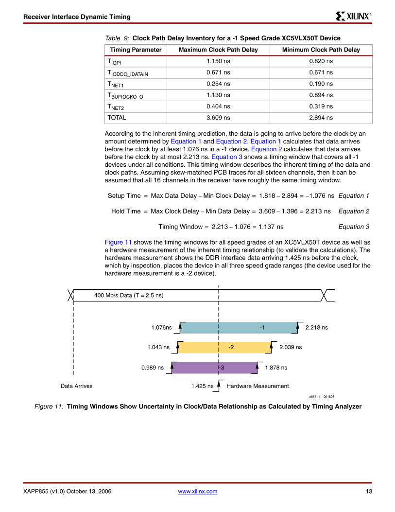
Receiver Interface Dynamic Timing
XAPP855 (v10) October 13 2006 wwwxilinxcom 13
R
According to the inherent timing prediction the data is going to arrive before the clock by an amount determined by Equation 1 and Equation 2 Equation 1 calculates that data arrives before the clock by at least 1076 ns in a -1 device Equation 2 calculates that data arrives before the clock by at most 2213 ns Equation 3 shows a timing window that covers all -1 devices under all conditions This timing window describes the inherent timing of the data and clock paths Assuming skew-matched PCB traces for all sixteen channels then it can be assumed that all 16 channels in the receiver have roughly the same timing window
Equation 1
Equation 2
Equation 3
Figure 11 shows the timing windows for all speed grades of an XC5VLX50T device as well as a hardware measurement of the inherent timing relationship (to validate the calculations) The hardware measurement shows the DDR interface data arriving 1425 ns before the clock which by inspection places the device in all three speed grade ranges (the device used for the hardware measurement is a -2 device)
Table 9 Clock Path Delay Inventory for a -1 Speed Grade XC5VLX50T Device
Timing Parameter Maximum Clock Path Delay Minimum Clock Path Delay
TIOPI 1150 ns 0820 ns
TIODDO_IDATAIN 0671 ns 0671 ns
TNET1 0254 ns 0190 ns
TBUFIOCKO_O 1130 ns 0894 ns
TNET2 0404 ns 0319 ns
TOTAL 3609 ns 2894 ns
Setup Time Max Data Delay Min Clock Delay 1818 2894ndash 1076 nsndash==ndash=
Hold Time Max Clock Delay Min Data Delay 3609 1396ndash 2213 ns==ndash=
Timing Window 2213 1076ndash 1137 ns==
Figure 11 Timing Windows Show Uncertainty in ClockData Relationship as Calculated by Timing Analyzer
400 Mbs Data (T = 25 ns)
1425 ns Hardware MeasurementData Arrives
x855_11_091806
-11076ns 2213 ns
-21043 ns 2039 ns
-30989 ns 1878 ns
Receiver Interface Dynamic Timing
XAPP855 (v10) October 13 2006 wwwxilinxcom 14
R
Dynamic Timing and BIT_ALIGN_MACHINE
In ldquoInherent Timingrdquo page 11 the inherent timing of the interface was calculated for all speed grades and validated with a hardware measurement In that case the inherent timing was sufficient because the data rate is only 400 Mbs (Figure 11 page 13) What happens when the data rate is increased such that the hold edge of the data window begins to shrink (Figure 12)
At 600 Mbs the inherent timing relationship is no longer adequate to meet timing because there are cases when the sampling clock edge is in the middle of the data transition As the data rates increase to 800 and 1000 Mbs the clock actually captures the data arriving one bit time later For designs that are sensitive to word alignment this is unacceptable
The solution to the suboptimal inherent timing is dynamic timing The BIT_ALIGN_MACHINE module in the receiver performs two functions of dynamic timing
bull Bit Alignment Position the sampling edge of the clock at the center of the data eye by adding delay to the datapaths
bull Word Alignment Ensure that the parallel data bits are in the correct order at the output of the ISERDES by using the bitslip function in the ISERDES
The steps of the bit-alignment procedure are shown in Figure 13 page 15 Each step of the algorithm can either add or subtract delay from the datapath All 16 channels are taken through this procedure independently This procedure measures one full data eye (in terms of 75 ps delay taps) and then returns to the center of the data eye Steps 1 and 2 are dedicated to moving through the partial eye of the initial timing while steps 3 and 4 are dedicated to measuring a full eye Step 5 is dedicated to positioning the clock edge at the center of the data eye
Figure 12 Inherent Timing Windows Shown in Relation to Multiple Data Rates
400 Mbs Data (T = 25 ns)
600 Mbs Data (T = 167 ns)
800 Mbs Data (T = 127 ns)
1000 Mbs Data (T = 10 ns)
-11076ns 2213 ns
-21043 ns 2039 ns
-30989 ns
1425 ns
1878 ns
Hardware MeasurementData Arrives
x855_12_091806
Receiver Interface Dynamic Timing
XAPP855 (v10) October 13 2006 wwwxilinxcom 15
R
Jitter is represented in Figure 13 as multiple transition lines Accounting for jitter is a crucial part of the algorithm In step 2 the first data transition is found If there is no jitter then the eye measurement can begin instantly after finding the transition However when jitter is considered the algorithm must find the first transition move through the transition and then begin looking for the second transition If the algorithm does not move through the first transition intelligently it runs the risk of falsely detecting the second transition
Once bit alignment is complete the order of the data bits can be adjusted to achieve word alignment The bit-alignment procedure ensures that data is being sampled correctly but the order of the data can be a few bits off from where the receiver expects it to be To correct this the bitslip feature of the ISERDES is used to slip bit times until the proper alignment is found For this feature to be useful a training pattern must be generated by the transmitter (as discussed in ldquoDDR Transmitterrdquo page 3) that the receiver can use to determine the proper word alignment In this reference design the training pattern is 00101100 (0x2C) This pattern is mostly arbitrary as many other patterns work just as well This pattern was chosen because a training pattern should behave electrically as much like real data as possible such that the center of the training eye is the center of the data eye Since real data contains strings of consecutive ones and zeros it is best for the training pattern to do the same For that reason a 0x2C pattern is better than an 0xAA pattern because it contains run lengths of 1 2 3 and 4 bit times
Table 10 page 16 shows the word-alignment process in the case where bit alignment completes with the data outputs set to 0x58 Since 0x58 is not the training pattern the receiver is looking for bitslip is asserted until 0x2C is found This reference design uses a 18 deserialization so there are only eight possible configurations of the parallel data outputs If bitslip is asserted infinitely the same eight configurations will repeat Bitslip in DDR mode is somewhat irregular because it does not simply rotate by one bit on every bitslip cycle This effect is inconsequential to the word-alignment procedure (see the Virtex-5 User Guide for more details)
Figure 13 Dynamic Bit-Alignment Procedure in BIT_ALIGN_MACHINE
Data 0
Data Arrives Before Clock
Data 1
x855_13_091806
Data 0 Data 1
Data 0 Data 1
Data 0 Data 1
Data 0 Data 1
Sampling Clock (Fixed Delay)
Return to Center of Eye
End Measuring Eye
Begin Measuring Eye
Find 1st Transition
Initial Timing1
2
3
4
5
Receiver Interface Dynamic Timing
XAPP855 (v10) October 13 2006 wwwxilinxcom 16
R
The FSM in the BIT_ALIGN_MACHINE module used to implement both bit and word alignment is shown in Figure 14 page 17 The FSM is divided into five sections loosely described as finding the first transition getting through the first transition finding the second transition returning to the center of the eye and word alignment
To get through the first transition effectively for all possible types of jitter two methods are used The first method pertains to random jitter If there is a lot of random jitter at the sampling point then the samples generated are not stable The algorithm detects this instability by comparing current samples to older samples and therefore knows where the transition begins and ends But what if the jitter is extremely deterministic The transition then has discreet crossing points such that within the transition there is very stable but incorrect data In this case the algorithm does not sense any instability and falsely concludes that the sampling point is not in the transition To address this case apart from evaluating stability the algorithm also evaluates the correctness of the data content by using the bitslip feature in the middle of the transition For example if the algorithm determines that the sampled data is stable it then asserts bitslip to look for the correct data If 0x2c is found within eight assertions of bitslip then the sampling point is not in the transition But if 0x2c is not found then the algorithm increments the data delay and repeats the transition test again
Table 10 Word Alignment in the DDR Receiver
Bitslip Cycle Data Value (Hex) Data Value (Bin) Description of Bitslip operation
1 58 0101 1000 ndash
2 0B 0000 1011 Rotate 3 bits to right
3 16 0001 0110 Rotate 1 bit to left
4 C2 1100 0010 Rotate 3 bits to right
5 85 1000 0101 Rotate 1 bit to left
6 B0 1011 0000 Rotate 3 bits to right
7 61 0110 0001 Rotate 1 bit to left
8 2C 0010 1100 Rotate 3 bits to right
Receiver Interface Dynamic Timing
XAPP855 (v10) October 13 2006 wwwxilinxcom 17
R
Figure 14 FSM in the BIT_ALIGN_MACHINE Module
TRANSITION_CHECK (01000)
First TransitionNot Detected
First TransitionNot Detected
First TransitionDetected
First TransitionDetected
Past the FirstTransition
Second TransitionNot Detected
Second TransitionDetected
Decrement DelayAgain
Bit AlignmentComplete
Still Samplingin Transition
INC_ONCE (01111)
SEARCH_PAT (01101)
IDLE (01100)
IDLE (10000)
RECHECK_TRANS (00010)
ONE_BITSLIP (00110)
INC_ONCE (01011)
WAIT_8_CYCLES (00100)
COUNT_1 (01110)
INC_ONCE (01001)
WAIT_8_CYCLES (00011)
IDLE (10010)
TRAINING_DONE (00111)
FIRST_SAMPLE (00001)
RESET (00000)
DEC_TO_HALF (01010)
WORD_ALIGN (00101)
X855_14_082806
Routine to Avoid False Detection of Second Transition
=CHECK_PATTERN
Receiver Interface Dynamic Timing
XAPP855 (v10) October 13 2006 wwwxilinxcom 18
R
Interface Timing Budget
In addition to sampling the data as closely as possible to the center of the data eye the actual size of the data eye is important By accurately predicting the size of the data eye in the receiver the overall performance ceiling of the interface can be inferred The ideal data eye width is the period of the data rate (for example TBit_Period = 100 ns for 1000 Mbs) Both the transmitter and receiver circuits have sources of error that subtract from the ideal data eye The equation for the eye width at the output of the transmitter is shown in Equation 4 TJITTER is the peak-to-peak jitter of the clock source driving the transmitter data bus and forwarded clock TDCD is the maximum duty cycle distortion of the clock tree driving the data bus and forwarded clock Skew is not considered in the transmitter or receiver because the receiver calibrates out skew between channels by performing alignment on each channel individually
Equation 4
Equation 5 calculates the width of the data eye at the receiver flip-flops Ideally the eye width at the receiver is the same as the eye width at the output of the transmitter but there are sources of error in the transmission medium and receiver circuitry Duty cycle distortion must be considered again on the receiver clock tree TSAMP_BUFIO is the receiver sampling error due to drift caused by voltage and temperature variations TIDELAYPAT_JIT is the amount of pattern dependent jitter that is accumulated in each tap of the IDELAY chain For a clock pattern TIDELAYPAT_JIT is 0 pstap peak to peak For a data pattern with long and short run lengths of zeroes and ones (simulated by PRBS23) TIDELAYPAT_JIT is a finite value that must be considered in the timing budget
Equation 5
TBOARD_JITTER includes jitter induced by receiver input capacitance and the parasitics of the physical data path on the PCB TBOARD_JITTER must be determined by simulation as it varies as a function of frequency and for receivers of different types and vendors On the ML550 with a -2 speed-grade Virtex-5 device the TBOARD_JITTER is measured at roughly 200 ps at 900 Mbs (assuming data content equivalent to PRBS23) TQUANTIZATION_ERR or quantization error is caused by the granularity of the IDELAY tap chain Working with 75 ps increments it is not possible to utilize the entire data eye since inevitably some valid eye width is lost between two taps The value for this loss is 75 ps As long as the receiver eye width calculated using Equation 5 is greater than or equal to 0 the interface operates correctly over process voltage and temperature
For example Equation 6 and Equation 7 show the timing budget calculation for the DDR interface running at 900 Mbs in a -2 speed grade device on an ML550 evaluation board Refer to the data sheet for the most current values The TX interface is looped back to the RX interface on the same Virtex-5 FPGA as shown in Equation 2
Equation 6
Equation 7
Changes in voltage and temperature cause the data channels of the interface to drift relative to the clock If the DDR interface were to transfer user data for a long period of time over all specified conditions of temperature and voltage Equation 7 states that there would be at least 107 ps (one or two IDELAY taps) of data window remaining valid during all fluctuations of temperature and voltage Compare this calculation to the measurements in Table 12 page 21 Case 900 Mbs There are four taps that are error free under all conditions In ldquoAppendixrdquo there are three -2 devices tested at 900 Mbs and each has 4 4 and 3 taps respectively that are error free under all conditions
DATA_EYE_WIDTH_TX TBIT_PERIOD TJITTERndash TDCD_BUFIOndash=
DATA_EYE_WIDTH_RX DATA_EYE_WIDTH_TX
TBOARD_JITTER
ndash
TSAMP_BUFIOndash TDCD_BUFIOndash
TIDELAYPAT_JIT IDELAY taps in datapathtimes[ ]ndash
TQUANTIZATION_ERRndash
=
DATA_EYE_WIDTH_TX 1111 ps 25 psndash 100 psndash 986 ps= =
DATA_EYE_WIDTH_RX986 ps 200 psndash 400 psndash 100 psndash 8 ps 13 tapstimes[ ] 75 ps 107 ps=ndashndash
=
Interface Characterization
XAPP855 (v10) October 13 2006 wwwxilinxcom 19
R
At a given temperature and voltage setting the data valid window is much larger because there is no drift when temperature and voltage are constant The size of the data valid window under constant conditions is 107 ps + TSAMP_BUFIO which in this case is at least 507 ps (six or seven IDELAY taps) Compare this calculation to the measurements of any single condition in Table 12 Case 900 Mbs In the worst case (ndash5 supply) there are 7 taps that are error free
Equation 8 and Equation 9 show the same timing budget calculation for the DDR interface running at 10 Gbs in a -2 speed grade device on an ML550 Evaluation Board
Equation 8
Equation 9
Equation 9 predicts that no data window remains valid during all specified fluctuations of temperature and voltage (compare to Table 12 Case 1000 Mbs) In ldquoAppendixrdquo there are three -2 devices tested at 1000 Mbs and each has 1 3 and 1 taps respectively that are error free under all conditions This data rate and device combination are very marginal cases
To operate at 10 Gbs the DDR interface requires additional circuitry to track out voltage-temperature variations in real-time (see XAPP860 16-channel DDR LVDS Interface with Real-time Window Monitoring for a DDR Interface with real-time window monitoring) If the voltage-temperature variations are removed from the picture the predicted data valid window is ndash120 ps + TSAMP_BUFIO which in this case is at least 280 ps (3 or 4 taps) Compare this calculation to the measurements of any single condition in Table 18 page 34 There are at least four error-free taps in all conditions
Interface Characterization
By following the procedure illustrated in Figure 13 page 15 the bit-alignment algorithm should never insert more than approximately 15 bit times of delay on the data channels The fewest number of delay taps should be used in the datapath because they produce a finite amount of degradation (TIDELAYPAT_JIT) The worst-case initial timing for the algorithm occurs when the clock samples just before the data transitions as in the 600 Mbs case in Figure 12 page 14 The algorithm must move all the way through the first eye to find the first transition (1 bit time) and then move halfway into the next eye to center the sampling point (05 bit time) This process produces a worst-case total delay insertion of 15 bit times
The actual performance of the bit-alignment algorithm is characterized as a function of data rate in Figure 15 page 20 For all data rates the expectation is that the tap settings of all 16 channels in the DDR receiver do not exceed approximately 15 bit times of delay Both the maximum and minimum tap setting of all 16 channels is recorded for each data rate This graph only shows the data for a single device Comparing the 15 bit time mask to the actual settings it is clear that the algorithm remains within the 15 bit time limit At 13 Gbs the tap setting actually exceeds the mask by one tap (a negligible violation)
DATA_EYE_WIDTH_TX 1000 ps 25 psndash 100 psndash 875 ps= =
DATA_EYE_WIDTH_RX 875 ps 300 psndash400 ps 100 psndash
ndash8 ps 15 tapstimes[ ] 75 ps 120 psndash=ndashndash
=
Interface Characterization
XAPP855 (v10) October 13 2006 wwwxilinxcom 20
R
The maximum and minimum tap settings in Figure 15 generally stay within 3 to 4 taps of each other except in the case of 640 Mbs and 1300 Mbs data rates These data rates are seams in the inherent timing At data rates below 640 Mbs the tap settings are in the range of 30 taps and at data rates above 640 Mbs the tap settings are in the range of 12 taps Referring back to Figure 12 page 14 it is clear why this seam occurs As the data rate increases past 600 Mbs the initial sampling point of the inherent timing moves into a different data eye creating a different starting point for the algorithm At 640 Mbs some of the 16 channels start in one eye while other channels start in the other eye Fortunately this is not an issue because the single bit time of difference between the channels is resolved using bitslip
Referring back to Figure 8 page 9 the clock channel goes through an IDELAY block with a default value of 0 Once the data rate is chosen for a given design this initial IDELAY value can be changed to a non-zero value to achieve more favorable inherent timing For example a design running at 620 Mbs can use 30 IDELAY taps on the delay channels each contributing a certain amount of jitter to the timing budget calculation By setting the initial clock delay to 5 taps the inherent timing moves across the seam shown in the 600 Mbs range of Figure 15 causing the data channels to only use about 12 IDELAY taps Only spectrally rich data patterns accumulate jitter in the IDELAY tap chain so the clock IDELAY can be set to any value without diminishing the timing budget This optimization is entirely optional and can be done once the design is running in hardware
The DDR receiver is designed to remove skew between channels by aligning each channel individually The ML550 board on which this reference design is characterized is designed to have minimal skew between channels However there is clearly a finite amount of skew between channels due to clock skew in the TX and RX BUFIO networks package skew and trace length tolerance on the ML550 board Table 11 page 21 shows how the bit-alignment algorithm sets the delay for each channel differently to compensate for skew between channels The table captures the range of settings among the 16 channels at specific data rates for a -2 device If there were additional skew among the 16 channels then the tap setting range would be larger to compensate for it The algorithm is designed such that skew between channels should not diminish the performance of the interface The range of tap settings differs for different devices and speed grades but the magnitude should be approximately the same
Figure 15 Bit-Alignment Algorithm Performance
60
50
40
30
20
10
0200 400 600 800 1000 1200 1400 1600
Data Rate (Mbs)
Del
ay T
ap U
tiliz
atio
n HW Measurement (Min)HW Measurement (Max)15 Bit Time Mask
X855_15_072406
Interface Characterization
XAPP855 (v10) October 13 2006 wwwxilinxcom 21
R
Since the receiver alignment logic only runs once immediately after reset the resulting dynamic timing must be adequate to ensure error-free operation over the specified voltage and temperature variations that can occur over time The data-valid window at the receiver input must be wide enough to withstand these variations (receiver drift) Table 12 page 21 shows the data-valid window at the ISERDES registers in the DDR receiver The eyes shown are collective eyes of all 16 channels The BERT testbench configuration loops back the DDR transmitter to the DDR receiver Using pattern generators and error detectors programmed to send and receive a pseudorandom bit sequence (PRBS23) the width of the data-valid window is evaluated using pseudorandom data that closely resembles real user data
Table 11 Tap Setting Range For Various Data Rates Measured on a -2 Device
Data Rate (Mbs) Tap Setting Range Compensated Skew
500 31ndash34 4 taps
600 28ndash30 3 taps
700 10ndash12 3 taps
800 11ndash13 3 taps
900 11ndash13 3 taps
1000 13ndash15 3 taps
1100 13ndash15 3 taps
1200 14ndash15 2 taps
Table 12 Measurement of Receiver Drift under Extreme Conditions for Multiple Data Rates
ConditionIODELAY Taps (1)
ndash8 ndash7 ndash6 ndash5 ndash4 ndash3 ndash2 ndash1 0 +1 +2 +3 +4 +5 +6 +7 +8
Case 800 Mbs
25degC Nom Supplies F F F P P P P P C P P P P P F F F
0degC Nom Supplies F F F P P P P P P P P P P P F F F
85degC Nom Supplies F F F P P P P P P P P P P P F F F
25degC +5 Supplies F P P P P P P P P P P P F F F F F
0degC +5 Supplies F P P P P P P P P P P P F F F F F
85degC +5 Supplies F P P P P P P P P P P P F F F F F
25degC ndash5 Supplies F F F F F F P P P P P P P P P F F
0degC ndash5 Supplies F F F F F F P P P P P P P P P P F
85degC ndash5 Supplies F F F F F P P P P P P P P P P F F
CONCLUSION Error free under all conditions when calibrated under nominal conditions to position C
Interface Characterization
XAPP855 (v10) October 13 2006 wwwxilinxcom 22
R
Case 900 Mbs
25degC Nom Supplies F F F F P P P P C P P P P F F F F
0degC Nom Supplies F F F F P P P P P P P P P F F F F
85degC Nom Supplies F F F F P P P P P P P P F F F F F
25degC +5 Supplies F F P P P P P P P P P F F F F F F
0degC +5 Supplies F F P P P P P P P P P F F F F F F
85degC +5 Supplies F F P P P P P P P P P F F F F F F
25degC ndash5 Supplies F F F F F F F P P P P P P P P F F
0degC ndash5 Supplies F F F F F F F P P P P P P P P F F
85degC ndash5 Supplies F F F F F F F P P P P P P P F F F
CONCLUSION Error free under all conditions when calibrated under nominal conditions to position C
Case 1000 Mbs
25degC Nom Supplies F F F F F P P P C P P P F F F F F
0degC Nom Supplies F F F F F P P P P P P P F F F F F
85degC Nom Supplies F F F F F P P P P P P P F F F F F
25degC +5 Supplies F F F P P P P P P P F F F F F F F
0degC +5 Supplies F F F P P P P P P P F F F F F F F
85degC +5 Supplies F F F P P P P P P P P F F F F F F
25degC ndash5 Supplies F F F F F F F F P P P P P P F F F
0degC ndash5 Supplies F F F F F F F F P P P P P P F F F
85degC ndash5 Supplies F F F F F F F F P P P P P P F F F
CONCLUSION Error free under all conditions when calibrated under nominal conditions to position C
Case 1100 Mbs
25degC Nom Supplies F F F F F P P P C P F F F F F F F
0degC Nom Supplies F F F F F P P P P P F F F F F F F
85degC Nom Supplies F F F F F P P P P P F F F F F F F
25degC +5 Supplies F F F P P P P P P F F F F F F F F
0degC +5 Supplies F F F P P P P P P F F F F F F F F
85degC +5 Supplies F F F P P P P P P F F F F F F F F
25degC ndash5 Supplies F F F F F F F F P P P P F F F F F
0degC ndash5 Supplies F F F F F F F F P P P P F F F F F
85degC ndash5 Supplies F F F F F F F F P P P P F F F F F
CONCLUSION Error free under all conditions when calibrated under nominal conditions to position C
Table 12 Measurement of Receiver Drift under Extreme Conditions for Multiple Data Rates (Continued)
ConditionIODELAY Taps (1)
ndash8 ndash7 ndash6 ndash5 ndash4 ndash3 ndash2 ndash1 0 +1 +2 +3 +4 +5 +6 +7 +8
Interface Characterization
XAPP855 (v10) October 13 2006 wwwxilinxcom 23
R
In all test cases shown in Table 12 page 21 the bit-align machine accurately places the sampling point in the center of the data eye (indicated by the C in each test case) In the 1100 Mbs case the bit-align machine places the sampling point slightly off center This slight inaccuracy occurs when the center of a real data pattern diverges from the center of the training pattern The electrical behavior of different data patterns is discussed below
After the dynamic timing is established for a given test case under nominal conditions the device is subjected to extremes of temperature and voltage to stress the receiver timing At data rates of 1100 Mbs and below the dynamic timing established after reset under nominal conditions is sufficient to meet timing over all specified extreme conditions (the column with the C passes traffic error free under all conditions) At a data rate of 1200 Mbs the design operates correctly under nominal conditions but the data-valid window is not large enough to withstand the voltage variations For this particular transmission medium the 1200 Mbs case requires a real-time adjustment circuit that could track the center of the eye
The full datapath of the testbench consists of
TX rarr 5 FR-4 rarr SAMTEC QSE Conn rarr 12 Ribbon Cable rarr SAMTEC QSE Conn rarr 5 FR-4 rarr RX
For shorter transmission media higher performance can be achieved in accordance with the section ldquoInterface Timing Budgetrdquo page 18 Interface performance is not solely a question of the LVDS driver performance specification but rather a question of adequate timing margin to withstand production and environmental variations From Table 12 the total amount of variation experienced over temperature and voltage is roughly 375 ps (5 taps at 75 ps per tap) This number should be comparable to the specification for receiver sampling error (TSAMP_BUFIO) shown in the Virtex-5 Data Sheet
Case 1200 Mbs
25degC Nom Supplies F F F F F F P P C P F F F F F F F
0degC Nom Supplies F F F F F F P P P P F F F F F F F
85degC Nom Supplies F F F F F F P P P F F F F F F F F
25degC +5 Supplies F F F F P P P P F F F F F F F F F
0degC +5 Supplies F F F P P P P P F F F F F F F F F
85degC +5 Supplies F F F F P P P P F F F F F F F F F
25degC ndash5 Supplies F F F F F F F F F P P P F F F F F
0degC ndash5 Supplies F F F F F F F F F P P P F F F F F
85degC ndash5 Supplies F F F F F F F F F P P F F F F F F
CONCLUSION Errors caused by plusmn5 variations in supply voltages
Notes 1 Where 0 is the reference tap determined by the bit-align machine under nominal conditions at 25degC2 P = Error-free transmission F = Error in transmission C = IODELAY tap position selected by bit-align machine under nominal conditions at 25degC3 Device under test is -2 speed grade
Table 12 Measurement of Receiver Drift under Extreme Conditions for Multiple Data Rates (Continued)
ConditionIODELAY Taps (1)
ndash8 ndash7 ndash6 ndash5 ndash4 ndash3 ndash2 ndash1 0 +1 +2 +3 +4 +5 +6 +7 +8
Interface Characterization
XAPP855 (v10) October 13 2006 wwwxilinxcom 24
R
Pattern Dependence of Receiver Performance
Different types of data patterns have different electrical signatures (rise and fall times jitter eye symmetry etc) A pattern with very narrow spectral content (such as a clock pattern) moves very favorably through the link because the receiver frequency response has little effect on the signal integrity However a pattern with wide spectral content (such as real data and pseudorandom patterns) stresses the links frequency response If the frequency response is not flat across the entire spectrum of the data content then the signal integrity is degraded as a result The amount of degradation measured is shown in Table 13 page 25 The DDR transmitter is looped back to the DDR receiver and different patterns are programmed to traverse the link Performance is assessed by evaluating the integrity of those patterns in the receiver
PRBS7 is a pseudorandom data pattern with a maximum run length of seven consecutive zeroes or ones PRBS15 is defined as having a maximum run length of fifteen consecutive zeroes or ones These limitations on run lengths limit the spectral content of the pattern A PRBS15 pattern has greater spectral content than a PRBS7 pattern and therefore is a more strenuous test for the link PRBS29 is the most strenuous test in Table 13 A clock pattern is effectively a PRBS1
As predicted Table 13 shows that there is more degradation for data patterns with more spectral content At 1000 Mbs and below the data eye closure is symmetrical Symmetrical eye closure is desired because it does not change the center of the eye as determined by the bit-alignment algorithm Above 1000 Mbs the eye closure becomes more asymmetrical causing the center of the data eye to diverge from the calibrated center (by only 1 tap)
In every data rate shown in Table 13 all significant pattern-dependent degradation is caused between PRBS1 (clock pat) and PRBS15 Between PRBS15 and PRBS29 there is no additional degradation recorded in any of the measurements
Interface Characterization
XAPP855 (v10) October 13 2006 wwwxilinxcom 25
R
Table 13 Link Performance for Various Types of Data Measured on a -2 Device
PatternIODELAY Taps (1)
ndash8 ndash7 ndash6 ndash5 ndash4 ndash3 ndash2 ndash1 0 +1 +2 +3 +4 +5 +6 +7 +8 +9
Case 600 Mbs
Clock Pat (0101) P P P P P P P P C P P P P P P P P P
Training Pat (0x2C) P P P P P P P P C P P P P P P P P F
PRBS7 P P P P P P P P C P P P P P P P P F
PRBS15 F P P P P P P P C P P P P P P P F F
PRBS23 F P P P P P P P C P P P P P P P F F
PRBS29 F P P P P P P P C P P P P P P P F F
Case 800 Mbs
Clock Pat (0101) F F P P P P P P C P P P P P P F F F
Training Pat (0x2C) F F P P P P P P C P P P P P P F F F
PRBS7 F F P P P P P P C P P P P P F F F F
PRBS15 F F F P P P P P C P P P P P F F F F
PRBS23 F F F P P P P P C P P P P P F F F F
PRBS29 F F F P P P P P C P P P P P F F F F
Case 1000 Mbs
Clock Pat (0101) F F F P P P P P C P P P P P F F F F
Training Pat (0x2C) F F F P P P P P C P P P P F F F F F
PRBS7 F F F F P P P P C P P P F F F F F F
PRBS15 F F F F F P P P C P P P F F F F F F
PRBS23 F F F F F P P P C P P P F F F F F F
PRBS29 F F F F F P P P C P P P F F F F F F
Case 1200 Mbs
Clock Pat (0101) F F F F P P P P C P P P P F F F F F
Training Pat (0x2C) F F F F P P P P C P P P F F F F F F
PRBS7 F F F F F P P P C P F F F F F F F F
PRBS15 F F F F F F P P C F F F F F F F F F
PRBS23 F F F F F F P P C F F F F F F F F F
PRBS29 F F F F F F P P C F F F F F F F F F
Case 1400 Mbs
Clock Pat (0101) F F F F F F P P C P P P F F F F F F
Training Pat (0x2C) F F F F F P P P C P P F F F F F F F
PRBS7 F F F F F F F P C P F F F F F F F F
PRBS15 F F F F F F F P C F F F F F F F F F
PRBS23 F F F F F F F P C F F F F F F F F F
PRBS29 F F F F F F F P C F F F F F F F F F
Notes 1 Where 0 is the reference tap determined by the bit-align machine under nominal conditions at 25degC2 P = Error-free transmission F = Error in transmission C = IODELAY tap position selected by bit-align machine under nominal conditions at 25degC
Resetting the Interface
XAPP855 (v10) October 13 2006 wwwxilinxcom 26
R
Resetting the Interface
Several dependencies determine the order in which circuits should be reset in the interface The receiver cannot begin the alignment algorithm if the transmitter is not sending the training pattern The transmitter must be reset before the receiver and time must be allowed for the training pattern to propagate across the link before the receiver comes out of reset The receiver also cannot begin the alignment algorithm until IDELAYCTRL has recovered from reset which could takes hundreds of cycles The recommended reset timing for the interface is shown in Figure 16 This reset timing is implemented in the BERT testbench for this interface
The TX reset (RST_TX) is used to reset all TX circuitry and also IDELAYCTRL The IDELAYCTRL reset is asynchronous so driving it with RST_TX is acceptable The minimum pulse width of IDELAYCTRL reset is 50 ns (TIDELAYCTRL_RPW) For that reason resets are held High for 16 clock cycles The RX reset (RST_RX) is used to reset all RX circuitry and is asserted when the IDELAYCTRL READY flag goes High indicating that the IODELAY blocks are calibrated
The timing of the READY flag in Figure 16 is a potential hazard Most likely it is High during a TX reset because it takes many cycles for IDELAYCTRL to deassert the READY flag It is easy to make the mistake of resetting the receiver too early To avoid this hazard the RX reset should be asserted only after seeing a deassertion and reassertion of the READY flag
Conclusion Based on the design and characterization described in this document the 16-Channel DDR reference design operates to the performance targets in Table 14 under all conditions of process voltage and temperature However to meet these targets over voltage and temperature the timing budget must be guaranteed according to the analysis in ldquoInterface Timing Budgetrdquo See ldquoAppendixrdquo page 27 for further justification of the maximum performance recommendations in Table 14
Figure 16 Recommended Interface Reset Timing
RST_TX
IDELAYCTRLREADY
RST_RX
16 Cycles X855_16_072406
Table 14 Performance of 16-Channel DDR Interface
Speed Grade Maximum Performance
-1 800 Mbs
-2 900 Mbs
-3 10 Gbs(1)
Notes 1 To achieve higher performance (up to 125 Gbs) see 16-channel DDR LVDS Interface with Realtime
Window Monitoring for an example of a DDR interface with real-time window monitoring
Appendix
XAPP855 (v10) October 13 2006 wwwxilinxcom 27
R
Appendix Performance Characterization Data
Refer to ldquoInterface Characterizationrdquo page 19 for explanations about how to interpret the data in the ldquoAppendixrdquo These tables show collective data eyes for the entire interface over process voltage and temperature (PVT) Three devices from each speed grade were selected for this characterization
The calibrated center position of the eye (marked by the C in the tables below) varies slightly from channel to channel (due to small skews between channels) That range is referred to as center tap range Analysis of Table 16 page 28 through Table 20 page 40 shows that the center tap range for slow and fast parts differ significantly at the same data rate (because the BIT_ALIGN_MACHINE algorithm adjusts for differences in speed)
All data in the ldquoAppendixrdquo is collected using the BERT testbench shown in Figure 2 page 2 The data pattern is PRBS23 and the devicepackage is XC5VLX50T-FF1136 The transmission path for the cases shown in Table 16 through Table 20 is repeated for convenience
TX rarr 5 FR-4 rarr SAMTEC QSE Conn rarr 12 Ribbon Cable rarr SAMTEC QSE Conn rarr 5 FR-4 rarr RX
A summary of these characterization results is shown in Table 15 Each of the nine parts were tested at 800 900 1000 1100 and 1200 Mbs When the interface is error free on all channels under all extreme conditions of temperature and voltage the particular test case is designated by a P A test case is marked FAIL when the interface suffered errors on any channel under any particular condition of voltage and temperature
Table 15 Summary of Interface Characterization Results
Device (SN) Speed Grade 800 Mbs 900 Mbs 1000Mbs 1100 Mbs 1200 Mbs
2194 -1 P P P FAIL FAIL
2219 -1 P FAIL FAIL FAIL FAIL
2199 -1 P P FAIL FAIL FAIL
001 -2 P P FAIL P FAIL
002 -2 P P P P FAIL
003 -2 P P FAIL FAIL FAIL
004 -3 P P P P P
005 -3 P P P P P
006 -3 P P P P P
Appendix
XAPP855 (v10) October 13 2006 wwwxilinxcom 28
R
Table 16 Measurement of Receiver Drift under Extreme Conditions at 800 Mbs
ConditionIODELAY Taps (1)
ndash8 ndash7 ndash6 ndash5 ndash4 ndash3 ndash2 ndash1 0 +1 +2 +3 +4 +5 +6 +7 +8
SN 2194 Speed Grade -1
25degC Nom Supplies F F F P P P P P C P P P P F F F F
0degC Nom Supplies F F F P P P P P P P P P P F F F F
85degC Nom Supplies F F F F P P P P P P P P P F F F F
25degC +5 Supplies F F P P P P P P P P P P F F F F F
0degC +5 Supplies F F P P P P P P P P P P F F F F F
85degC +5 Supplies F F P P P P P P P P P P F F F F F
25degC ndash5 Supplies F F F F F F P P P P P P P P P F F
0degC ndash5 Supplies F F F F F F P P P P P P P P P F F
85degC ndash5 Supplies F F F F F F P P P P P P P P P F F
Center Tap Range Taps 11ndash12
CONCLUSION Error free under all conditions when calibrated under nominal conditions to position C
SN 2219 Speed Grade -1
25degC Nom Supplies F F F P P P P P C P P P F F F F F
0degC Nom Supplies F F F P P P P P P P P P F F F F F
85degC Nom Supplies F F F P P P P P P P P P F F F F F
25degC +5 Supplies F P P P P P P P P P P F F F F F F
0degC +5 Supplies F P P P P P P P P P P F F F F F F
85degC +5 Supplies F P P P P P P P P P P F F F F F F
25degC ndash5 Supplies F F F F F F P P P P P P P P F F F
0degC ndash5 Supplies F F F F F F F P P P P P P P F F F
85degC ndash5 Supplies F F F F F F P P P P P P P P F F F
Center Tap Range Taps 13ndash16
CONCLUSION Error free under all conditions when calibrated under nominal conditions to position C
SN 2199 Speed Grade -1
25degC Nom Supplies F F F P P P P P C P P P P F F F F
0degC Nom Supplies F F F P P P P P P P P P P F F F F
85degC Nom Supplies F F F P P P P P P P P P P F F F F
25degC +5 Supplies F P P P P P P P P P P P F F F F F
0degC +5 Supplies F P P P P P P P P P P P F F F F F
85degC +5 Supplies F P P P P P P P P P P P F F F F F
25degC ndash5 Supplies F F F F F F P P P P P P P P P F F
0degC ndash5 Supplies F F F F F F P P P P P P P P P F F
85degC ndash5 Supplies F F F F F F P P P P P P P P P F F
Center Tap Range Taps 10ndash12
CONCLUSION Error free under all conditions when calibrated under nominal conditions to position C
Appendix
XAPP855 (v10) October 13 2006 wwwxilinxcom 29
R
SN 001 Speed Grade -2
25degC Nom Supplies F F F P P P P P C P P P P F F F F
0degC Nom Supplies F F F P P P P P P P P P P F F F F
85degC Nom Supplies F F F P P P P P P P P P P F F F F
25degC +5 Supplies F P P P P P P P P P P P F F F F F
0degC +5 Supplies F P P P P P P P P P P F F F F F F
85degC +5 Supplies F P P P P P P P P P P P F F F F F
25degC ndash5 Supplies F F F F F P P P P P P P P P P F F
0degC ndash5 Supplies F F F F F P P P P P P P P P P F F
85degC ndash5 Supplies F F F F F P P P P P P P P P P F F
Center Tap Range Taps 10ndash12
CONCLUSION Error free under all conditions when calibrated under nominal conditions to position C
SN 002 Speed Grade -2
25degC Nom Supplies F F F P P P P P C P P P P F F F F
0degC Nom Supplies F F F P P P P P P P P P P F F F F
85degC Nom Supplies F F F P P P P P P P P P P F F F F
25degC +5 Supplies F P P P P P P P P P P P F F F F F
0degC +5 Supplies F P P P P P P P P P P P F F F F F
85degC +5 Supplies F F P P P P P P P P P P F F F F F
25degC ndash5 Supplies F F F F F P P P P P P P P P P F F
0degC ndash5 Supplies F F F F F P P P P P P P P P P F F
85degC ndash5 Supplies F F F F F P P P P P P P P P P F F
Center Tap Range Taps 10ndash12
CONCLUSION Error free under all conditions when calibrated under nominal conditions to position C
SN 003 Speed Grade -2
25degC Nom Supplies F F F P P P P P C P P P P F F F F
0degC Nom Supplies F F F P P P P P P P P P P F F F F
85degC Nom Supplies F F F P P P P P P P P P P F F F F
25degC +5 Supplies F P P P P P P P P P P P F F F F F
0degC +5 Supplies F P P P P P P P P P P F F F F F F
85degC +5 Supplies F P P P P P P P P P P P F F F F F
25degC ndash5 Supplies F F F F F F P P P P P P P P P F F
0degC ndash5 Supplies F F F F F F P P P P P P P P P F F
85degC ndash5 Supplies F F F F F F P P P P P P P P P F F
Center Tap Range Taps 11ndash13
CONCLUSION Error free under all conditions when calibrated under nominal conditions to position C
Table 16 Measurement of Receiver Drift under Extreme Conditions at 800 Mbs (Continued)
ConditionIODELAY Taps (1)
ndash8 ndash7 ndash6 ndash5 ndash4 ndash3 ndash2 ndash1 0 +1 +2 +3 +4 +5 +6 +7 +8
Appendix
XAPP855 (v10) October 13 2006 wwwxilinxcom 30
R
SN 004 Speed Grade -3
25degC Nom Supplies F F F P P P P P C P P P P F F F F
0degC Nom Supplies F F F P P P P P P P P P F F F F F
85degC Nom Supplies F F F P P P P P P P P P P F F F F
25degC +5 Supplies F P P P P P P P P P P P F F F F F
0degC +5 Supplies F P P P P P P P P P P P F F F F F
85degC +5 Supplies F F P P P P P P P P P P F F F F F
25degC ndash5 Supplies F F F F F P P P P P P P P P F F F
0degC ndash5 Supplies F F F F F P P P P P P P P P F F F
85degC ndash5 Supplies F F F F F P P P P P P P P P F F F
Center Tap Range Taps 8ndash9 23ndash24
CONCLUSION Error free under all conditions when calibrated under nominal conditions to position C
SN 005 Speed Grade -3
25degC Nom Supplies F F P P P P P P C P P P P F F F F
0degC Nom Supplies F F P P P P P P P P P P P F F F F
85degC Nom Supplies F F F P P P P P P P P P P P F F F
25degC +5 Supplies F P P P P P P P P P P P F F F F F
0degC +5 Supplies F P P P P P P P P P P P F F F F F
85degC +5 Supplies F P P P P P P P P P P P F F F F F
25degC ndash5 Supplies F F F F P P P P P P P P P P P F F
0degC ndash5 Supplies F F F F P P P P P P P P P P P F F
85degC ndash5 Supplies F F F F P P P P P P P P P P P F F
Center Tap Range Taps 9ndash10
CONCLUSION Error free under all conditions when calibrated under nominal conditions to position C
SN 006 Speed Grade -3
25degC Nom Supplies F F P P P P P P C P P P P F F F F
0degC Nom Supplies F F P P P P P P P P P P P F F F F
85degC Nom Supplies F F F P P P P P P P P P P F F F F
25degC +5 Supplies F P P P P P P P P P P P F F F F F
0degC +5 Supplies F P P P P P P P P P P P F F F F F
85degC +5 Supplies F F P P P P P P P P P P F F F F F
25degC ndash5 Supplies F F F P P P P P P P P P P P F F F
0degC ndash5 Supplies F F F P P P P P P P P P P P F F F
85degC ndash5 Supplies F F F F F P P P P P P P P P F F F
Center Tap Range Taps 8ndash9 23ndash24
CONCLUSION Error free under all conditions when calibrated under nominal conditions to position C
Notes 1 IODELAY taps where 0 is the reference tap determined by the bit align machine at nominal voltage and 25degC2 P = Error-free transmission F = Error in transmission C = IODELAY tap position selected by bit-align machine under nominal conditions at 25degC
Table 16 Measurement of Receiver Drift under Extreme Conditions at 800 Mbs (Continued)
ConditionIODELAY Taps (1)
ndash8 ndash7 ndash6 ndash5 ndash4 ndash3 ndash2 ndash1 0 +1 +2 +3 +4 +5 +6 +7 +8
Appendix
XAPP855 (v10) October 13 2006 wwwxilinxcom 31
R
Table 17 Measurement of Receiver Drift under Extreme Conditions at 900 Mbs
ConditionIODELAY Taps (1)
ndash8 ndash7 ndash6 ndash5 ndash4 ndash3 ndash2 ndash1 0 +1 +2 +3 +4 +5 +6 +7 +8
SN 2194 Speed Grade -1
25degC Nom Supplies F F F F F P P P C P P P F F F F F
0degC Nom Supplies F F F F F P P P P P P P F F F F F
85degC Nom Supplies F F F F F P P P P P P P P F F F F
25degC +5 Supplies F F F P P P P P P P P F F F F F F
0degC +5 Supplies F F F P P P P P P P P F F F F F F
85degC +5 Supplies F F F P P P P P P P P F F F F F F
25degC ndash5 Supplies F F F F F F F P P P P P P P F F F
0degC ndash5 Supplies F F F F F F F P P P P P P P F F F
85degC ndash5 Supplies F F F F F F F P P P P P P P F F F
Center Tap Range Taps 11ndash12
CONCLUSION Error free under all conditions when calibrated under nominal conditions to position C
SN 2219 Speed Grade -1
25degC Nom Supplies F F F F F P P P C P P P F F F F F
0degC Nom Supplies F F F F F P P P P P P P F F F F F
85degC Nom Supplies F F F F F P P P P P P P F F F F F
25degC +5 Supplies F F F P P P P P P P F F F F F F F
0degC +5 Supplies F F F P P P P P P P F F F F F F F
85degC +5 Supplies F F F P P P P P P P F F F F F F F
25degC ndash5 Supplies F F F F F F F F F P P P P P F F F
0degC ndash5 Supplies F F F F F F F F F P P P P P F F F
85degC ndash5 Supplies F F F F F F F F P P P P P P F F F
Center Tap Range Taps 12ndash15
CONCLUSION Errors caused by ndash5 variation in supply voltage
SN 2199 Speed Grade -1
25degC Nom Supplies F F F F F P P P C P P P F F F F F
0degC Nom Supplies F F F F F P P P P P P P F F F F F
85degC Nom Supplies F F F F F P P P P P P P F F F F F
25degC +5 Supplies F F F P P P P P P P P F F F F F F
0degC +5 Supplies F F F P P P P P P P P F F F F F F
85degC +5 Supplies F F F P P P P P P P P F F F F F F
25degC ndash5 Supplies F F F F F F F F P P P P P P F F F
0degC ndash5 Supplies F F F F F F F F P P P P P P F F F
85degC ndash5 Supplies F F F F F F F F P P P P P P F F F
Center Tap Range Taps 10ndash12
CONCLUSION Error free under all conditions when calibrated under nominal conditions to position C
Appendix
XAPP855 (v10) October 13 2006 wwwxilinxcom 32
R
SN 001 Speed Grade -2
25degC Nom Supplies F F F F P P P P C P P P P F F F F
0degC Nom Supplies F F F F P P P P P P P P P F F F F
85degC Nom Supplies F F F F F P P P P P P P P F F F F
25degC +5 Supplies F F P P P P P P P P P F F F F F F
0degC +5 Supplies F F P P P P P P P P P F F F F F F
85degC +5 Supplies F F F P P P P P P P P P F F F F F
25degC ndash5 Supplies F F F F F F F P P P P P P P F F F
0degC ndash5 Supplies F F F F F F F P P P P P P P F F F
85degC ndash5 Supplies F F F F F F F P P P P P P P F F F
Center Tap Range Taps 9ndash11
CONCLUSION Error free under all conditions when calibrated under nominal conditions to position C
SN 002 Speed Grade -2
25degC Nom Supplies F F F F P P P P C P P P P F F F F
0degC Nom Supplies F F F F P P P P P P P P F F F F F
85degC Nom Supplies F F F F F P P P P P P P P F F F F
25degC +5 Supplies F F F P P P P P P P P F F F F F F
0degC +5 Supplies F F F P P P P P P P P F F F F F F
85degC +5 Supplies F F F P P P P P P P P P F F F F F
25degC ndash5 Supplies F F F F F F F P P P P P P P F F F
0degC ndash5 Supplies F F F F F F F P P P P P P P F F F
85degC ndash5 Supplies F F F F F F F P P P P P P P F F F
Center Tap Range Taps 10ndash12
CONCLUSION Error free under all conditions when calibrated under nominal conditions to position C
SN 003 Speed Grade -2
25degC Nom Supplies F F F F F P P P C P P P P F F F F
0degC Nom Supplies F F F F F P P P P P P P P F F F F
85degC Nom Supplies F F F F F P P P P P P P P F F F F
25degC +5 Supplies F F P P P P P P P P P F F F F F F
0degC +5 Supplies F F P P P P P P P P P F F F F F F
85degC +5 Supplies F F F P P P P P P P P F F F F F F
25degC ndash5 Supplies F F F F F F F P P P P P P P F F F
0degC ndash5 Supplies F F F F F F F F P P P P P P F F F
85degC ndash5 Supplies F F F F F F F P P P P P P P F F F
Center Tap Range Taps 11ndash13
CONCLUSION Error free under all conditions when calibrated under nominal conditions to position C
Table 17 Measurement of Receiver Drift under Extreme Conditions at 900 Mbs (Continued)
ConditionIODELAY Taps (1)
ndash8 ndash7 ndash6 ndash5 ndash4 ndash3 ndash2 ndash1 0 +1 +2 +3 +4 +5 +6 +7 +8
Appendix
XAPP855 (v10) October 13 2006 wwwxilinxcom 33
R
SN 004 Speed Grade -3
25degC Nom Supplies F F F F P P P P C P P P P F F F F
0degC Nom Supplies F F F P P P P P P P P P P F F F F
85degC Nom Supplies F F F F P P P P P P P P P F F F F
25degC +5 Supplies F F F P P P P P P P P P F F F F F
0degC +5 Supplies F F F P P P P P P P P P F F F F F
85degC +5 Supplies F F F P P P P P P P P P F F F F F
25degC ndash5 Supplies F F F F F F P P P P P P P P F F F
0degC ndash5 Supplies F F F F F F P P P P P P P P F F F
85degC ndash5 Supplies F F F F F F P P P P P P P P F F F
Center Tap Range Taps 7ndash8
CONCLUSION Error free under all conditions when calibrated under nominal conditions to position C
SN 005 Speed Grade ndash3
25degC Nom Supplies F F F P P P P P C P P P P F F F F
0degC Nom Supplies F F F P P P P P P P P P P F F F F
85degC Nom Supplies F F F F P P P P P P P P P F F F F
25degC +5 Supplies F F P P P P P P P P P P F F F F F
0degC +5 Supplies F F P P P P P P P P P P F F F F F
85degC +5 Supplies F F F P P P P P P P P P F F F F F
25degC ndash5 Supplies F F F F F F P P P P P P P P F F F
0degC ndash5 Supplies F F F F F P P P P P P P P P F F F
85degC ndash5 Supplies F F F F F F P P P P P P P P F F F
Center Tap Range Taps 9ndash10
CONCLUSION Error free under all conditions when calibrated under nominal conditions to position C
SN 006 Speed Grade -3
25degC Nom Supplies F F F F P P P P C P P P P F F F F
0degC Nom Supplies F F F F P P P P P P P P P F F F F
85degC Nom Supplies F F F F P P P P P P P P P F F F F
25degC +5 Supplies F F P P P P P P P P P P F F F F F
0degC +5 Supplies F F P P P P P P P P P P F F F F F
85degC +5 Supplies F F F P P P P P P P P P F F F F F
25degC ndash5 Supplies F F F F F P P P P P P P P P F F F
0degC ndash5 Supplies F F F F F P P P P P P P P P F F F
85degC ndash5 Supplies F F F F F F P P P P P P P P F F F
Center Tap Range Taps 7ndash8
CONCLUSION Error free under all conditions when calibrated under nominal conditions to position C
Notes 1 IODELAY taps where 0 is the reference tap determined by the bit align machine at nominal voltage and 25degC2 P = Error-free transmission F = Error in transmission C = IODELAY tap position selected by bit-align machine under nominal conditions at 25degC
Table 17 Measurement of Receiver Drift under Extreme Conditions at 900 Mbs (Continued)
ConditionIODELAY Taps (1)
ndash8 ndash7 ndash6 ndash5 ndash4 ndash3 ndash2 ndash1 0 +1 +2 +3 +4 +5 +6 +7 +8
Appendix
XAPP855 (v10) October 13 2006 wwwxilinxcom 34
R
Table 18 Measurement of Receiver Drift under Extreme Conditions at 1000 Mbs
ConditionIODELAY Taps (1)
ndash8 ndash7 ndash6 ndash5 ndash4 ndash3 ndash2 ndash1 0 +1 +2 +3 +4 +5 +6 +7 +8
SN 2194 Speed Grade -1
25degC Nom Supplies F F F F F P P P C P P F F F F F F
0degC Nom Supplies F F F F F P P P P P P F F F F F F
85degC Nom Supplies F F F F F P P P P P P F F F F F F
25degC +5 Supplies F F F P P P P P P P F F F F F F F
0degC +5 Supplies F F F P P P P P P P F F F F F F F
85degC +5 Supplies F F F F P P P P P P F F F F F F F
25degC ndash5 Supplies F F F F F F F F P P P P P F F F F
0degC ndash5 Supplies F F F F F F F F P P P P P F F F F
85degC ndash5 Supplies F F F F F F F F P P P P P F F F F
Center Tap Range Taps 12ndash13
CONCLUSION Error free under all conditions when calibrated under nominal conditions to position C
SN 2219 Speed Grade -1
25degC Nom Supplies F F F F F F P P C P P F F F F F F
0degC Nom Supplies F F F F F F P P P P P F F F F F F
85degC Nom Supplies F F F F F F P P P P P F F F F F F
25degC +5 Supplies F F F P P P P P P F F F F F F F F
0degC +5 Supplies F F F P P P P P P F F F F F F F F
85degC +5 Supplies F F F F P P P P P F F F F F F F F
25degC ndash5 Supplies F F F F F F F F F P P P P F F F F
0degC ndash5 Supplies F F F F F F F F F F P P P F F F F
85degC ndash5 Supplies F F F F F F F F F P P P P F F F F
Center Tap Range Taps 14ndash17
CONCLUSION Errors caused by ndash5 variation in supply voltage
SN 2199 Speed Grade -1
25degC Nom Supplies F F F F F F P P C P P F F F F F F
0degC Nom Supplies F F F F F F P P P P P F F F F F F
85degC Nom Supplies F F F F F F P P P P P F F F F F F
25degC +5 Supplies F F F F P P P P P P F F F F F F F
0degC +5 Supplies F F F F P P P P P P F F F F F F F
85degC +5 Supplies F F F F P P P P P P F F F F F F F
25degC ndash5 Supplies F F F F F F F F F P P P P F F F F
0degC ndash5 Supplies F F F F F F F F F P P P P F F F F
85degC ndash5 Supplies F F F F F F F F F P P P P F F F F
Center Tap Range Taps 12ndash14
CONCLUSION Errors caused by ndash5 variation in supply voltage
Appendix
XAPP855 (v10) October 13 2006 wwwxilinxcom 35
R
SN 001 Speed Grade -2
25degC Nom Supplies F F F F F F P P C P P P F F F F F
0degC Nom Supplies F F F F F F P P P P P P F F F F F
85degC Nom Supplies F F F F F F P P P P P P F F F F F
25degC +5 Supplies F F F F P P P P P P F F F F F F F
0degC +5 Supplies F F F F P P P P P P F F F F F F F
85degC +5 Supplies F F F F P P P P P P P F F F F F F
25degC ndash5 Supplies F F F F F F F F F P P P P F F F F
0degC ndash5 Supplies F F F F F F F F F P P P P F F F F
85degC ndash5 Supplies F F F F F F F F F P P P P F F F F
Center Tap Range Taps 11ndash12
CONCLUSION Errors caused by ndash5 variation in supply voltage
SN 002 Speed Grade -2
25degC Nom Supplies F F F F F P P P C P P F F F F F F
0degC Nom Supplies F F F F F P P P P P P P F F F F F
85degC Nom Supplies F F F F F P P P P P P P F F F F F
25degC +5 Supplies F F F F P P P P P P F F F F F F F
0degC +5 Supplies F F F P P P P P P P F F F F F F F
85degC +5 Supplies F F F F P P P P P P P F F F F F F
25degC ndash5 Supplies F F F F F F F P P P P P P F F F F
0degC ndash5 Supplies F F F F F F F P P P P P P F F F F
85degC ndash5 Supplies F F F F F F F P P P P P P F F F F
Center Tap Range Taps 11ndash13
CONCLUSION Error free under all conditions when calibrated under nominal conditions to position C
SN 003 Speed Grade -2
25degC Nom Supplies F F F F F F P P C P P F F F F F F
0degC Nom Supplies F F F F F F P P P P P F F F F F F
85degC Nom Supplies F F F F F F P P P P P F F F F F F
25degC +5 Supplies F F F F P P P P P P F F F F F F F
0degC +5 Supplies F F F F P P P P P P F F F F F F F
85degC +5 Supplies F F F F P P P P P P F F F F F F F
25degC ndash5 Supplies F F F F F F F F F P P P P F F F F
0degC ndash5 Supplies F F F F F F F F F P P P P F F F F
85degC ndash5 Supplies F F F F F F F F F P P P P F F F F
Center Tap Range Taps 13ndash14
CONCLUSION Errors caused by ndash5 variation in supply voltage
Table 18 Measurement of Receiver Drift under Extreme Conditions at 1000 Mbs (Continued)
ConditionIODELAY Taps (1)
ndash8 ndash7 ndash6 ndash5 ndash4 ndash3 ndash2 ndash1 0 +1 +2 +3 +4 +5 +6 +7 +8
Appendix
XAPP855 (v10) October 13 2006 wwwxilinxcom 36
R
SN 004 Speed Grade -3
25degC Nom Supplies F F F F F P P P C P P P F F F F F
0degC Nom Supplies F F F F F P P P P P P P F F F F F
85degC Nom Supplies F F F F F P P P P P P P F F F F F
25degC +5 Supplies F F F P P P P P P P P F F F F F F
0degC +5 Supplies F F F P P P P P P P P F F F F F F
85degC +5 Supplies F F F F P P P P P P P P F F F F F
25degC ndash5 Supplies F F F F F F F P P P P P P F F F F
0degC ndash5 Supplies F F F F F F F P P P P P P F F F F
85degC ndash5 Supplies F F F F F F F P P P P P P P F F F
Center Tap Range Taps 9ndash10
CONCLUSION Error free under all conditions when calibrated under nominal conditions to position C
SN 005 Speed Grade -3
25degC Nom Supplies F F F F P P P P C P P P F F F F F
0degC Nom Supplies F F F F P P P P P P P P F F F F F
85degC Nom Supplies F F F F P P P P P P P P F F F F F
25degC +5 Supplies F F F P P P P P P P P F F F F F F
0degC +5 Supplies F F P P P P P P P P P F F F F F F
85degC +5 Supplies F F F P P P P P P P P F F F F F F
25degC ndash5 Supplies F F F F F F P P P P P P P P F F F
0degC ndash5 Supplies F F F F F F P P P P P P P P F F F
85degC ndash5 Supplies F F F F F F P P P P P P P F F F F
Center Tap Range Taps 11ndash12
CONCLUSION Error free under all conditions when calibrated under nominal conditions to position C
SN 006 Speed Grade -3
25degC Nom Supplies F F F F P P P P C P P P F F F F F
0degC Nom Supplies F F F F P P P P P P P P F F F F F
85degC Nom Supplies F F F F P P P P P P P P F F F F F
25degC +5 Supplies F F F P P P P P P P P F F F F F F
0degC +5 Supplies F F F P P P P P P P P F F F F F F
85degC +5 Supplies F F F P P P P P P P P F F F F F F
25degC ndash5 Supplies F F F F F F P P P P P P P F F F F
0degC ndash5 Supplies F F F F F F P P P P P P P F F F F
85degC ndash5 Supplies F F F F F F P P P P P P P F F F F
Center Tap Range Taps 9ndash10
CONCLUSION Error free under all conditions when calibrated under nominal conditions to position C
Notes 1 IODELAY taps where 0 is the reference tap determined by the bit align machine at nominal voltage and 25degC2 P = Error-free transmission F = Error in transmission C = IODELAY tap position selected by bit-align machine under nominal conditions at 25degC
Table 18 Measurement of Receiver Drift under Extreme Conditions at 1000 Mbs (Continued)
ConditionIODELAY Taps (1)
ndash8 ndash7 ndash6 ndash5 ndash4 ndash3 ndash2 ndash1 0 +1 +2 +3 +4 +5 +6 +7 +8
Appendix
XAPP855 (v10) October 13 2006 wwwxilinxcom 37
R
Table 19 Measurement of Receiver Drift under Extreme Conditions at 1100 Mbs
ConditionIODELAY Taps (1)
ndash8 ndash7 ndash6 ndash5 ndash4 ndash3 ndash2 ndash1 0 +1 +2 +3 +4 +5 +6 +7 +8
SN 2194 Speed Grade -1
25degC Nom Supplies F F F F F F P P C P P F F F F F F
0degC Nom Supplies F F F F F F P P P P P F F F F F F
85degC Nom Supplies F F F F F F P P P P P F F F F F F
25degC +5 Supplies F F F F P P P P P F F F F F F F F
0degC +5 Supplies F F F F P P P P P F F F F F F F F
85degC +5 Supplies F F F F P P P P P F F F F F F F F
25degC ndash5 Supplies F F F F F F F F F P P P F F F F F
0degC ndash5 Supplies F F F F F F F F F P P P F F F F F
85degC ndash5 Supplies F F F F F F F F F P P P F F F F F
Center Tap Range Taps 13ndash14
CONCLUSION Errors caused by ndash5 variation in supply voltage
SN 2219 Speed Grade -1
25degC Nom Supplies F F F F F F P P C P F F F F F F F
0degC Nom Supplies F F F F F F P P P P F F F F F F F
85degC Nom Supplies F F F F F F P P P P F F F F F F F
25degC +5 Supplies F F F F P P P P F F F F F F F F F
0degC +5 Supplies F F F F P P P P F F F F F F F F F
85degC +5 Supplies F F F F P P P P F F F F F F F F F
25degC ndash5 Supplies F F F F F F F F F F P P F F F F F
0degC ndash5 Supplies F F F F F F F F F F P P F F F F F
85degC ndash5 Supplies F F F F F F F F F P P P F F F F F
Center Tap Range Taps 6 15ndash17
CONCLUSION Errors caused by plusmn5 variation in supply voltage
SN 2199 Speed Grade -1
25degC Nom Supplies F F F F F F F P C P F F F F F F F
0degC Nom Supplies F F F F F F F P P P F F F F F F F
85degC Nom Supplies F F F F F F F P P P F F F F F F F
25degC +5 Supplies F F F F P P P P P F F F F F F F F
0degC +5 Supplies F F F F P P P P P F F F F F F F F
85degC +5 Supplies F F F F F P P P P F F F F F F F F
25degC ndash5 Supplies F F F F F F F F F F P P F F F F F
0degC ndash5 Supplies F F F F F F F F F F P P F F F F F
85degC ndash5 Supplies F F F F F F F F F F P P F F F F F
Center Tap Range Taps 13ndash15
CONCLUSION Errors caused by ndash5 variation in supply voltage
Appendix
XAPP855 (v10) October 13 2006 wwwxilinxcom 38
R
SN 001 Speed Grade -2
25degC Nom Supplies F F F F F F P P C P P F F F F F F
0degC Nom Supplies F F F F F F P P P P P F F F F F F
85degC Nom Supplies F F F F F F P P P P P F F F F F F
25degC +5 Supplies F F F F P P P P P F F F F F F F F
0degC +5 Supplies F F F F P P P P P F F F F F F F F
85degC +5 Supplies F F F F P P P P P F F F F F F F F
25degC ndash5 Supplies F F F F F F F F P P P P F F F F F
0degC ndash5 Supplies F F F F F F F F P P P P F F F F F
85degC ndash5 Supplies F F F F F F F F P P P P F F F F F
Center Tap Range Taps 12ndash13
CONCLUSION Error free under all conditions when calibrated under nominal conditions to position C
SN 002 Speed Grade -2
25degC Nom Supplies F F F F F P P P C P F F F F F F F
0degC Nom Supplies F F F F F P P P P P F F F F F F F
85degC Nom Supplies F F F F F F P P P P F F F F F F F
25degC +5 Supplies F F F F P P P P P F F F F F F F F
0degC +5 Supplies F F F P P P P P P F F F F F F F F
85degC +5 Supplies F F F F P P P P P F F F F F F F F
25degC ndash5 Supplies F F F F F F F F P P P P F F F F F
0degC ndash5 Supplies F F F F F F F F P P P P F F F F F
85degC ndash5 Supplies F F F F F F F F P P P P F F F F F
Center Tap Range Taps 13ndash14
CONCLUSION Error free under all conditions when calibrated under nominal conditions to position C
SN 003 Speed Grade -2
25degC Nom Supplies F F F F F F F P C P F F F F F F F
0degC Nom Supplies F F F F F F F P P P F F F F F F F
85degC Nom Supplies F F F F F F F P P P P F F F F F F
25degC +5 Supplies F F F F F P P P P F F F F F F F F
0degC +5 Supplies F F F F F P P P P F F F F F F F F
85degC +5 Supplies F F F F F P P P P F F F F F F F F
25degC ndash5 Supplies F F F F F F F F F F P P F F F F F
0degC ndash5 Supplies F F F F F F F F F F P P F F F F F
85degC ndash5 Supplies F F F F F F F F F P P P F F F F F
Center Tap Range Taps 14ndash16
CONCLUSION Errors caused by ndash5 variation in supply voltage
Table 19 Measurement of Receiver Drift under Extreme Conditions at 1100 Mbs (Continued)
ConditionIODELAY Taps (1)
ndash8 ndash7 ndash6 ndash5 ndash4 ndash3 ndash2 ndash1 0 +1 +2 +3 +4 +5 +6 +7 +8
Appendix
XAPP855 (v10) October 13 2006 wwwxilinxcom 39
R
SN 004 Speed Grade -3
25degC Nom Supplies F F F F F P P P C P P F F F F F F
0degC Nom Supplies F F F F F P P P P P P F F F F F F
85degC Nom Supplies F F F F F F P P P P P F F F F F F
25degC +5 Supplies F F F F P P P P P P F F F F F F F
0degC +5 Supplies F F F F P P P P P P F F F F F F F
85degC +5 Supplies F F F F P P P P P P F F F F F F F
25degC ndash5 Supplies F F F F F F F F P P P P F F F F F
0degC ndash5 Supplies F F F F F F F P P P P P F F F F F
85degC ndash5 Supplies F F F F F F F F P P P P P F F F F
Center Tap Range Taps 9ndash10
CONCLUSION Error free under all conditions when calibrated under nominal conditions to position C
SN 005 Speed Grade -3
25degC Nom Supplies F F F F F P P P C P P F F F F F F
0degC Nom Supplies F F F F F P P P P P P F F F F F F
85degC Nom Supplies F F F F F F P P P P P F F F F F F
25degC +5 Supplies F F F F P P P P P P F F F F F F F
0degC +5 Supplies F F F F P P P P P P F F F F F F F
85degC +5 Supplies F F F F P P P P P P F F F F F F F
25degC ndash5 Supplies F F F F F F F P P P P P P F F F F
0degC ndash5 Supplies F F F F F F F P P P P P P F F F F
85degC ndash5 Supplies F F F F F F F P P P P P P F F F F
Center Tap Range Taps 11ndash12
CONCLUSION Error free under all conditions when calibrated under nominal conditions to position C
SN 006 Speed Grade -3
25degC Nom Supplies F F F F F P P P C P P P F F F F F
0degC Nom Supplies F F F F F P P P P P P F F F F F F
85degC Nom Supplies F F F F F P P P P P P P F F F F F
25degC +5 Supplies F F F F P P P P P P P F F F F F F
0degC +5 Supplies F F F P P P P P P P F F F F F F F
85degC +5 Supplies F F F F P P P P P P P F F F F F F
25degC ndash5 Supplies F F F F F F P P P P P P P F F F F
0degC ndash5 Supplies F F F F F F P P P P P P P F F F F
85degC ndash5 Supplies F F F F F F F P P P P P P F F F F
Center Tap Range Taps 9ndash10
CONCLUSION Error free under all conditions when calibrated under nominal conditions to position C
Notes 1 IODELAY taps where 0 is the reference tap determined by the bit align machine at nominal voltage and 25degC2 P = Error-free transmission F = Error in transmission C = IODELAY tap position selected by bit-align machine under nominal conditions at 25degC
Table 19 Measurement of Receiver Drift under Extreme Conditions at 1100 Mbs (Continued)
ConditionIODELAY Taps (1)
ndash8 ndash7 ndash6 ndash5 ndash4 ndash3 ndash2 ndash1 0 +1 +2 +3 +4 +5 +6 +7 +8
Appendix
XAPP855 (v10) October 13 2006 wwwxilinxcom 40
R
Table 20 Measurement of Receiver Drift under Extreme Conditions at 1200 Mbs
ConditionIODELAY Taps (1)
ndash8 ndash7 ndash6 ndash5 ndash4 ndash3 ndash2 ndash1 0 +1 +2 +3 +4 +5 +6 +7 +8
SN 2194 Speed Grade -1
25degC Nom Supplies F F F F F F F P C F F F F F F F F
0degC Nom Supplies F F F F F F F P P F F F F F F F F
85degC Nom Supplies F F F F F F F P P F F F F F F F F
25degC +5 Supplies F F F F P P P P F F F F F F F F F
0degC +5 Supplies F F F F P P P P F F F F F F F F F
85degC +5 Supplies F F F F F P P P F F F F F F F F F
25degC ndash5 Supplies F F F F F F F F F P P F F F F F F
0degC ndash5 Supplies F F F F F F F F F F P F F F F F F
85degC ndash5 Supplies F F F F F F F F F P F F F F F F F
Center Tap Range Taps 13ndash15
CONCLUSION Errors caused by plusmn5 variation in supply voltage
SN 2219 Speed Grade -1
25degC Nom Supplies F F F F F F F F C F F F F F F F F
0degC Nom Supplies F F F F F F F P P F F F F F F F F
85degC Nom Supplies F F F F F F F F P F F F F F F F F
25degC +5 Supplies F F F F F P P P F F F F F F F F F
0degC +5 Supplies F F F F F P P P F F F F F F F F F
85degC +5 Supplies F F F F F F P P F F F F F F F F F
25degC ndash5 Supplies F F F F F F F F F F F F F F F F F
0degC ndash5 Supplies F F F F F F F F F F F F F F F F F
85degC ndash5 Supplies F F F F F F F F F F F F F F F F F
Center Tap Range Taps 6ndash7 16ndash17
CONCLUSION Errors caused by plusmn5 variation in supply voltage
SN 2199 Speed Grade -1
25degC Nom Supplies F F F F F F F P C F F F F F F F F
0degC Nom Supplies F F F F F F F P P F F F F F F F F
85degC Nom Supplies F F F F F F F F P F F F F F F F F
25degC +5 Supplies F F F F F P P P F F F F F F F F F
0degC +5 Supplies F F F F F P P P F F F F F F F F F
85degC +5 Supplies F F F F F P P P F F F F F F F F F
25degC ndash5 Supplies F F F F F F F F F F F F F F F F F
0degC ndash5 Supplies F F F F F F F F F F F F F F F F F
85degC ndash5 Supplies F F F F F F F F F F F F F F F F F
Center Tap Range Taps 13ndash15
CONCLUSION Errors caused by plusmn5 variation in supply voltage
Appendix
XAPP855 (v10) October 13 2006 wwwxilinxcom 41
R
SN 001 Speed Grade -2
25degC Nom Supplies F F F F F F F P C P F F F F F F F
0degC Nom Supplies F F F F F F F P P P F F F F F F F
85degC Nom Supplies F F F F F F F P P P F F F F F F F
25degC +5 Supplies F F F F F P P P P F F F F F F F F
0degC +5 Supplies F F F F P P P P P F F F F F F F F
85degC +5 Supplies F F F F F P P P P F F F F F F F F
25degC ndash5 Supplies F F F F F F F F F F P F F F F F F
0degC ndash5 Supplies F F F F F F F F F F P F F F F F F
85degC ndash5 Supplies F F F F F F F F F F P F F F F F F
Center Tap Range Taps 12ndash13
CONCLUSION Errors caused by ndash5 variation in supply voltage
SN 002 Speed Grade -2
25degC Nom Supplies F F F F F F P P C P F F F F F F F
0degC Nom Supplies F F F F F F P P P P F F F F F F F
85degC Nom Supplies F F F F F F F P P P F F F F F F F
25degC +5 Supplies F F F F P P P P F F F F F F F F F
0degC +5 Supplies F F F F P P P P F F F F F F F F F
85degC +5 Supplies F F F F F P P P F F F F F F F F F
25degC ndash5 Supplies F F F F F F F F P P P F F F F F F
0degC ndash5 Supplies F F F F F F F F P P P F F F F F F
85degC ndash5 Supplies F F F F F F F F F P P F F F F F F
Center Tap Range Taps 13ndash14
CONCLUSION Errors caused by plusmn5 variation in supply voltage
SN 003 Speed Grade -2
25degC Nom Supplies F F F F F F F P C F F F F F F F F
0degC Nom Supplies F F F F F F F P P F F F F F F F F
85degC Nom Supplies F F F F F F F F P F F F F F F F F
25degC +5 Supplies F F F F F P P P F F F F F F F F F
0degC +5 Supplies F F F F F P P P F F F F F F F F F
85degC +5 Supplies F F F F F F P P F F F F F F F F F
25degC ndash5 Supplies F F F F F F F F F F F F F F F F F
0degC ndash5 Supplies F F F F F F F F F F F F F F F F F
85degC ndash5 Supplies F F F F F F F F F F F F F F F F F
Center Tap Range Taps 14ndash15
CONCLUSION Errors caused by plusmn5 variation in supply voltage
Table 20 Measurement of Receiver Drift under Extreme Conditions at 1200 Mbs (Continued)
ConditionIODELAY Taps (1)
ndash8 ndash7 ndash6 ndash5 ndash4 ndash3 ndash2 ndash1 0 +1 +2 +3 +4 +5 +6 +7 +8
Appendix
XAPP855 (v10) October 13 2006 wwwxilinxcom 42
R
SN 004 Speed Grade -3
25degC Nom Supplies F F F F F F P P C P F F F F F F F
0degC Nom Supplies F F F F F P P P P P F F F F F F F
85degC Nom Supplies F F F F F F P P P P F F F F F F F
25degC +5 Supplies F F F F P P P P P F F F F F F F F
0degC +5 Supplies F F F F P P P P P F F F F F F F F
85degC +5 Supplies F F F F F P P P P F F F F F F F F
25degC ndash5 Supplies F F F F F F F F P P P F F F F F F
0degC ndash5 Supplies F F F F F F F F P P P F F F F F F
85degC ndash5 Supplies F F F F F F F F P P P F F F F F F
Center Tap Range Taps 9ndash11
CONCLUSION Error free under all conditions when calibrated under nominal conditions to position C
SN 005 Speed Grade -3
25degC Nom Supplies F F F F F P P P C P F F F F F F F
0degC Nom Supplies F F F F F P P P P P F F F F F F F
85degC Nom Supplies F F F F F F P P P P F F F F F F F
25degC +5 Supplies F F F F P P P P P F F F F F F F F
0degC +5 Supplies F F F P P P P P P F F F F F F F F
85degC +5 Supplies F F F F P P P P P F F F F F F F F
25degC ndash5 Supplies F F F F F F F P P P P P F F F F F
0degC ndash5 Supplies F F F F F F F P P P P P F F F F F
85degC ndash5 Supplies F F F F F F F F P P P F F F F F F
Center Tap Range Taps 11ndash13
CONCLUSION Error free under all conditions when calibrated under nominal conditions to position C
SN 006 Speed Grade -3
25degC Nom Supplies F F F F F P P P C P F F F F F F F
0degC Nom Supplies F F F F F P P P P P F F F F F F F
85degC Nom Supplies F F F F F P P P P P F F F F F F F
25degC +5 Supplies F F F P P P P P P F F F F F F F F
0degC +5 Supplies F F F P P P P P P F F F F F F F F
85degC +5 Supplies F F F F P P P P P F F F F F F F F
25degC ndash5 Supplies F F F F F F F P P P P F F F F F F
0degC ndash5 Supplies F F F F F F P P P P P F F F F F F
85degC ndash5 Supplies F F F F F F F P P P P F F F F F F
Center Tap Range Taps 10ndash11
CONCLUSION Error free under all conditions when calibrated under nominal conditions to position C
Notes 1 IODELAY taps where 0 is the reference tap determined by the bit align machine at nominal voltage and 25degC2 P = Error-free transmission F = Error in transmission C = IODELAY tap position selected by bit-align machine under nominal conditions at 25degC
Table 20 Measurement of Receiver Drift under Extreme Conditions at 1200 Mbs (Continued)
ConditionIODELAY Taps (1)
ndash8 ndash7 ndash6 ndash5 ndash4 ndash3 ndash2 ndash1 0 +1 +2 +3 +4 +5 +6 +7 +8
Revision History
XAPP855 (v10) October 13 2006 wwwxilinxcom 43
R
Revision History
The following table shows the revision history for this document
Date Version Revision
101306 10 Initial Xilinx release
- 16-Channel DDR LVDS Interface with Per-Channel Alignment
-
- Summary
- Introduction
-
- Figure 1 Full-Duplex 16-Channel DDR Link between a Virtex-5 Device and Another Device with a 16-Channel DDR Interface
- Figure 2 BERT Testbench for Hardware Verification of the DDR Interface
- Figure 3 Design Hierarchy of the Interface (TX and RX)
-
- DDR Transmitter
-
- Table 1 DDR_8TO1_16CHAN_TX Module Port Definitions
- Figure 4 MasterSlave OSERDES Pair for a Single Data Channel with 81 Serialization
- Figure 5 Block Diagram of TX Interface
- Table 2 DDR TX Interface Utilization Statistics
-
- Interface Clocking
-
- Figure 6 Global and Regional Clocking Schemes in Virtex-5 FPGAs
- Table 3 Comparison of Global and IO Clock Performance by Speed Grade
-
- DDR Receiver
-
- Table 4 DDR_8TO1_16CHAN_RX Module Port Definitions
- Figure 7 MasterSlave ISERDES Pair for a Single Data Channel with 18 Deserialization
- Figure 8 Block Diagram of RX Interface
- Table 5 DDR RX Interface Utilization Statistics
-
- Receiver Interface Dynamic Timing
-
- Inherent Timing
-
- Figure 9 Timing Components of RX Data and Clock Paths
- Figure 10 ISE Timing Analyzer Properties Used in this Document
- Table 6 Datapath Timing Definitions
- Table 7 Clock Path Timing Definitions
- Table 8 Datapath Delay Inventory for a -1 Speed Grade XC5VLX50T Device
- Table 9 Clock Path Delay Inventory for a -1 Speed Grade XC5VLX50T Device
- Figure 11 Timing Windows Show Uncertainty in ClockData Relationship as Calculated by Timing Analyzer
-
- Dynamic Timing and BIT_ALIGN_MACHINE
-
- Figure 12 Inherent Timing Windows Shown in Relation to Multiple Data Rates
- Figure 13 Dynamic Bit-Alignment Procedure in BIT_ALIGN_MACHINE
- Table 10 Word Alignment in the DDR Receiver
- Figure 14 FSM in the BIT_ALIGN_MACHINE Module
-
- Interface Timing Budget
-
- Interface Characterization
-
- Figure 15 Bit-Alignment Algorithm Performance
- Table 11 Tap Setting Range For Various Data Rates Measured on a -2 Device
- Table 12 Measurement of Receiver Drift under Extreme Conditions for Multiple Data Rates
- Pattern Dependence of Receiver Performance
-
- Table 13 Link Performance for Various Types of Data Measured on a -2 Device
-
- Resetting the Interface
-
- Figure 16 Recommended Interface Reset Timing
-
- Conclusion
-
- Table 14 Performance of 16-Channel DDR Interface
-
- Appendix
-
- Performance Characterization Data
-
- Table 15 Summary of Interface Characterization Results
- Table 16 Measurement of Receiver Drift under Extreme Conditions at 800 Mbs
- Table 17 Measurement of Receiver Drift under Extreme Conditions at 900 Mbs
- Table 18 Measurement of Receiver Drift under Extreme Conditions at 1000 Mbs
- Table 19 Measurement of Receiver Drift under Extreme Conditions at 1100 Mbs
- Table 20 Measurement of Receiver Drift under Extreme Conditions at 1200 Mbs
-
- Revision History
-
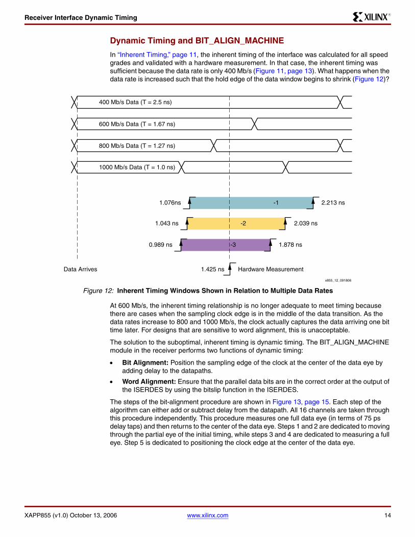
Receiver Interface Dynamic Timing
XAPP855 (v10) October 13 2006 wwwxilinxcom 15
R
Jitter is represented in Figure 13 as multiple transition lines Accounting for jitter is a crucial part of the algorithm In step 2 the first data transition is found If there is no jitter then the eye measurement can begin instantly after finding the transition However when jitter is considered the algorithm must find the first transition move through the transition and then begin looking for the second transition If the algorithm does not move through the first transition intelligently it runs the risk of falsely detecting the second transition
Once bit alignment is complete the order of the data bits can be adjusted to achieve word alignment The bit-alignment procedure ensures that data is being sampled correctly but the order of the data can be a few bits off from where the receiver expects it to be To correct this the bitslip feature of the ISERDES is used to slip bit times until the proper alignment is found For this feature to be useful a training pattern must be generated by the transmitter (as discussed in ldquoDDR Transmitterrdquo page 3) that the receiver can use to determine the proper word alignment In this reference design the training pattern is 00101100 (0x2C) This pattern is mostly arbitrary as many other patterns work just as well This pattern was chosen because a training pattern should behave electrically as much like real data as possible such that the center of the training eye is the center of the data eye Since real data contains strings of consecutive ones and zeros it is best for the training pattern to do the same For that reason a 0x2C pattern is better than an 0xAA pattern because it contains run lengths of 1 2 3 and 4 bit times
Table 10 page 16 shows the word-alignment process in the case where bit alignment completes with the data outputs set to 0x58 Since 0x58 is not the training pattern the receiver is looking for bitslip is asserted until 0x2C is found This reference design uses a 18 deserialization so there are only eight possible configurations of the parallel data outputs If bitslip is asserted infinitely the same eight configurations will repeat Bitslip in DDR mode is somewhat irregular because it does not simply rotate by one bit on every bitslip cycle This effect is inconsequential to the word-alignment procedure (see the Virtex-5 User Guide for more details)
Figure 13 Dynamic Bit-Alignment Procedure in BIT_ALIGN_MACHINE
Data 0
Data Arrives Before Clock
Data 1
x855_13_091806
Data 0 Data 1
Data 0 Data 1
Data 0 Data 1
Data 0 Data 1
Sampling Clock (Fixed Delay)
Return to Center of Eye
End Measuring Eye
Begin Measuring Eye
Find 1st Transition
Initial Timing1
2
3
4
5
Receiver Interface Dynamic Timing
XAPP855 (v10) October 13 2006 wwwxilinxcom 16
R
The FSM in the BIT_ALIGN_MACHINE module used to implement both bit and word alignment is shown in Figure 14 page 17 The FSM is divided into five sections loosely described as finding the first transition getting through the first transition finding the second transition returning to the center of the eye and word alignment
To get through the first transition effectively for all possible types of jitter two methods are used The first method pertains to random jitter If there is a lot of random jitter at the sampling point then the samples generated are not stable The algorithm detects this instability by comparing current samples to older samples and therefore knows where the transition begins and ends But what if the jitter is extremely deterministic The transition then has discreet crossing points such that within the transition there is very stable but incorrect data In this case the algorithm does not sense any instability and falsely concludes that the sampling point is not in the transition To address this case apart from evaluating stability the algorithm also evaluates the correctness of the data content by using the bitslip feature in the middle of the transition For example if the algorithm determines that the sampled data is stable it then asserts bitslip to look for the correct data If 0x2c is found within eight assertions of bitslip then the sampling point is not in the transition But if 0x2c is not found then the algorithm increments the data delay and repeats the transition test again
Table 10 Word Alignment in the DDR Receiver
Bitslip Cycle Data Value (Hex) Data Value (Bin) Description of Bitslip operation
1 58 0101 1000 ndash
2 0B 0000 1011 Rotate 3 bits to right
3 16 0001 0110 Rotate 1 bit to left
4 C2 1100 0010 Rotate 3 bits to right
5 85 1000 0101 Rotate 1 bit to left
6 B0 1011 0000 Rotate 3 bits to right
7 61 0110 0001 Rotate 1 bit to left
8 2C 0010 1100 Rotate 3 bits to right
Receiver Interface Dynamic Timing
XAPP855 (v10) October 13 2006 wwwxilinxcom 17
R
Figure 14 FSM in the BIT_ALIGN_MACHINE Module
TRANSITION_CHECK (01000)
First TransitionNot Detected
First TransitionNot Detected
First TransitionDetected
First TransitionDetected
Past the FirstTransition
Second TransitionNot Detected
Second TransitionDetected
Decrement DelayAgain
Bit AlignmentComplete
Still Samplingin Transition
INC_ONCE (01111)
SEARCH_PAT (01101)
IDLE (01100)
IDLE (10000)
RECHECK_TRANS (00010)
ONE_BITSLIP (00110)
INC_ONCE (01011)
WAIT_8_CYCLES (00100)
COUNT_1 (01110)
INC_ONCE (01001)
WAIT_8_CYCLES (00011)
IDLE (10010)
TRAINING_DONE (00111)
FIRST_SAMPLE (00001)
RESET (00000)
DEC_TO_HALF (01010)
WORD_ALIGN (00101)
X855_14_082806
Routine to Avoid False Detection of Second Transition
=CHECK_PATTERN
Receiver Interface Dynamic Timing
XAPP855 (v10) October 13 2006 wwwxilinxcom 18
R
Interface Timing Budget
In addition to sampling the data as closely as possible to the center of the data eye the actual size of the data eye is important By accurately predicting the size of the data eye in the receiver the overall performance ceiling of the interface can be inferred The ideal data eye width is the period of the data rate (for example TBit_Period = 100 ns for 1000 Mbs) Both the transmitter and receiver circuits have sources of error that subtract from the ideal data eye The equation for the eye width at the output of the transmitter is shown in Equation 4 TJITTER is the peak-to-peak jitter of the clock source driving the transmitter data bus and forwarded clock TDCD is the maximum duty cycle distortion of the clock tree driving the data bus and forwarded clock Skew is not considered in the transmitter or receiver because the receiver calibrates out skew between channels by performing alignment on each channel individually
Equation 4
Equation 5 calculates the width of the data eye at the receiver flip-flops Ideally the eye width at the receiver is the same as the eye width at the output of the transmitter but there are sources of error in the transmission medium and receiver circuitry Duty cycle distortion must be considered again on the receiver clock tree TSAMP_BUFIO is the receiver sampling error due to drift caused by voltage and temperature variations TIDELAYPAT_JIT is the amount of pattern dependent jitter that is accumulated in each tap of the IDELAY chain For a clock pattern TIDELAYPAT_JIT is 0 pstap peak to peak For a data pattern with long and short run lengths of zeroes and ones (simulated by PRBS23) TIDELAYPAT_JIT is a finite value that must be considered in the timing budget
Equation 5
TBOARD_JITTER includes jitter induced by receiver input capacitance and the parasitics of the physical data path on the PCB TBOARD_JITTER must be determined by simulation as it varies as a function of frequency and for receivers of different types and vendors On the ML550 with a -2 speed-grade Virtex-5 device the TBOARD_JITTER is measured at roughly 200 ps at 900 Mbs (assuming data content equivalent to PRBS23) TQUANTIZATION_ERR or quantization error is caused by the granularity of the IDELAY tap chain Working with 75 ps increments it is not possible to utilize the entire data eye since inevitably some valid eye width is lost between two taps The value for this loss is 75 ps As long as the receiver eye width calculated using Equation 5 is greater than or equal to 0 the interface operates correctly over process voltage and temperature
For example Equation 6 and Equation 7 show the timing budget calculation for the DDR interface running at 900 Mbs in a -2 speed grade device on an ML550 evaluation board Refer to the data sheet for the most current values The TX interface is looped back to the RX interface on the same Virtex-5 FPGA as shown in Equation 2
Equation 6
Equation 7
Changes in voltage and temperature cause the data channels of the interface to drift relative to the clock If the DDR interface were to transfer user data for a long period of time over all specified conditions of temperature and voltage Equation 7 states that there would be at least 107 ps (one or two IDELAY taps) of data window remaining valid during all fluctuations of temperature and voltage Compare this calculation to the measurements in Table 12 page 21 Case 900 Mbs There are four taps that are error free under all conditions In ldquoAppendixrdquo there are three -2 devices tested at 900 Mbs and each has 4 4 and 3 taps respectively that are error free under all conditions
DATA_EYE_WIDTH_TX TBIT_PERIOD TJITTERndash TDCD_BUFIOndash=
DATA_EYE_WIDTH_RX DATA_EYE_WIDTH_TX
TBOARD_JITTER
ndash
TSAMP_BUFIOndash TDCD_BUFIOndash
TIDELAYPAT_JIT IDELAY taps in datapathtimes[ ]ndash
TQUANTIZATION_ERRndash
=
DATA_EYE_WIDTH_TX 1111 ps 25 psndash 100 psndash 986 ps= =
DATA_EYE_WIDTH_RX986 ps 200 psndash 400 psndash 100 psndash 8 ps 13 tapstimes[ ] 75 ps 107 ps=ndashndash
=
Interface Characterization
XAPP855 (v10) October 13 2006 wwwxilinxcom 19
R
At a given temperature and voltage setting the data valid window is much larger because there is no drift when temperature and voltage are constant The size of the data valid window under constant conditions is 107 ps + TSAMP_BUFIO which in this case is at least 507 ps (six or seven IDELAY taps) Compare this calculation to the measurements of any single condition in Table 12 Case 900 Mbs In the worst case (ndash5 supply) there are 7 taps that are error free
Equation 8 and Equation 9 show the same timing budget calculation for the DDR interface running at 10 Gbs in a -2 speed grade device on an ML550 Evaluation Board
Equation 8
Equation 9
Equation 9 predicts that no data window remains valid during all specified fluctuations of temperature and voltage (compare to Table 12 Case 1000 Mbs) In ldquoAppendixrdquo there are three -2 devices tested at 1000 Mbs and each has 1 3 and 1 taps respectively that are error free under all conditions This data rate and device combination are very marginal cases
To operate at 10 Gbs the DDR interface requires additional circuitry to track out voltage-temperature variations in real-time (see XAPP860 16-channel DDR LVDS Interface with Real-time Window Monitoring for a DDR Interface with real-time window monitoring) If the voltage-temperature variations are removed from the picture the predicted data valid window is ndash120 ps + TSAMP_BUFIO which in this case is at least 280 ps (3 or 4 taps) Compare this calculation to the measurements of any single condition in Table 18 page 34 There are at least four error-free taps in all conditions
Interface Characterization
By following the procedure illustrated in Figure 13 page 15 the bit-alignment algorithm should never insert more than approximately 15 bit times of delay on the data channels The fewest number of delay taps should be used in the datapath because they produce a finite amount of degradation (TIDELAYPAT_JIT) The worst-case initial timing for the algorithm occurs when the clock samples just before the data transitions as in the 600 Mbs case in Figure 12 page 14 The algorithm must move all the way through the first eye to find the first transition (1 bit time) and then move halfway into the next eye to center the sampling point (05 bit time) This process produces a worst-case total delay insertion of 15 bit times
The actual performance of the bit-alignment algorithm is characterized as a function of data rate in Figure 15 page 20 For all data rates the expectation is that the tap settings of all 16 channels in the DDR receiver do not exceed approximately 15 bit times of delay Both the maximum and minimum tap setting of all 16 channels is recorded for each data rate This graph only shows the data for a single device Comparing the 15 bit time mask to the actual settings it is clear that the algorithm remains within the 15 bit time limit At 13 Gbs the tap setting actually exceeds the mask by one tap (a negligible violation)
DATA_EYE_WIDTH_TX 1000 ps 25 psndash 100 psndash 875 ps= =
DATA_EYE_WIDTH_RX 875 ps 300 psndash400 ps 100 psndash
ndash8 ps 15 tapstimes[ ] 75 ps 120 psndash=ndashndash
=
Interface Characterization
XAPP855 (v10) October 13 2006 wwwxilinxcom 20
R
The maximum and minimum tap settings in Figure 15 generally stay within 3 to 4 taps of each other except in the case of 640 Mbs and 1300 Mbs data rates These data rates are seams in the inherent timing At data rates below 640 Mbs the tap settings are in the range of 30 taps and at data rates above 640 Mbs the tap settings are in the range of 12 taps Referring back to Figure 12 page 14 it is clear why this seam occurs As the data rate increases past 600 Mbs the initial sampling point of the inherent timing moves into a different data eye creating a different starting point for the algorithm At 640 Mbs some of the 16 channels start in one eye while other channels start in the other eye Fortunately this is not an issue because the single bit time of difference between the channels is resolved using bitslip
Referring back to Figure 8 page 9 the clock channel goes through an IDELAY block with a default value of 0 Once the data rate is chosen for a given design this initial IDELAY value can be changed to a non-zero value to achieve more favorable inherent timing For example a design running at 620 Mbs can use 30 IDELAY taps on the delay channels each contributing a certain amount of jitter to the timing budget calculation By setting the initial clock delay to 5 taps the inherent timing moves across the seam shown in the 600 Mbs range of Figure 15 causing the data channels to only use about 12 IDELAY taps Only spectrally rich data patterns accumulate jitter in the IDELAY tap chain so the clock IDELAY can be set to any value without diminishing the timing budget This optimization is entirely optional and can be done once the design is running in hardware
The DDR receiver is designed to remove skew between channels by aligning each channel individually The ML550 board on which this reference design is characterized is designed to have minimal skew between channels However there is clearly a finite amount of skew between channels due to clock skew in the TX and RX BUFIO networks package skew and trace length tolerance on the ML550 board Table 11 page 21 shows how the bit-alignment algorithm sets the delay for each channel differently to compensate for skew between channels The table captures the range of settings among the 16 channels at specific data rates for a -2 device If there were additional skew among the 16 channels then the tap setting range would be larger to compensate for it The algorithm is designed such that skew between channels should not diminish the performance of the interface The range of tap settings differs for different devices and speed grades but the magnitude should be approximately the same
Figure 15 Bit-Alignment Algorithm Performance
60
50
40
30
20
10
0200 400 600 800 1000 1200 1400 1600
Data Rate (Mbs)
Del
ay T
ap U
tiliz
atio
n HW Measurement (Min)HW Measurement (Max)15 Bit Time Mask
X855_15_072406
Interface Characterization
XAPP855 (v10) October 13 2006 wwwxilinxcom 21
R
Since the receiver alignment logic only runs once immediately after reset the resulting dynamic timing must be adequate to ensure error-free operation over the specified voltage and temperature variations that can occur over time The data-valid window at the receiver input must be wide enough to withstand these variations (receiver drift) Table 12 page 21 shows the data-valid window at the ISERDES registers in the DDR receiver The eyes shown are collective eyes of all 16 channels The BERT testbench configuration loops back the DDR transmitter to the DDR receiver Using pattern generators and error detectors programmed to send and receive a pseudorandom bit sequence (PRBS23) the width of the data-valid window is evaluated using pseudorandom data that closely resembles real user data
Table 11 Tap Setting Range For Various Data Rates Measured on a -2 Device
Data Rate (Mbs) Tap Setting Range Compensated Skew
500 31ndash34 4 taps
600 28ndash30 3 taps
700 10ndash12 3 taps
800 11ndash13 3 taps
900 11ndash13 3 taps
1000 13ndash15 3 taps
1100 13ndash15 3 taps
1200 14ndash15 2 taps
Table 12 Measurement of Receiver Drift under Extreme Conditions for Multiple Data Rates
ConditionIODELAY Taps (1)
ndash8 ndash7 ndash6 ndash5 ndash4 ndash3 ndash2 ndash1 0 +1 +2 +3 +4 +5 +6 +7 +8
Case 800 Mbs
25degC Nom Supplies F F F P P P P P C P P P P P F F F
0degC Nom Supplies F F F P P P P P P P P P P P F F F
85degC Nom Supplies F F F P P P P P P P P P P P F F F
25degC +5 Supplies F P P P P P P P P P P P F F F F F
0degC +5 Supplies F P P P P P P P P P P P F F F F F
85degC +5 Supplies F P P P P P P P P P P P F F F F F
25degC ndash5 Supplies F F F F F F P P P P P P P P P F F
0degC ndash5 Supplies F F F F F F P P P P P P P P P P F
85degC ndash5 Supplies F F F F F P P P P P P P P P P F F
CONCLUSION Error free under all conditions when calibrated under nominal conditions to position C
Interface Characterization
XAPP855 (v10) October 13 2006 wwwxilinxcom 22
R
Case 900 Mbs
25degC Nom Supplies F F F F P P P P C P P P P F F F F
0degC Nom Supplies F F F F P P P P P P P P P F F F F
85degC Nom Supplies F F F F P P P P P P P P F F F F F
25degC +5 Supplies F F P P P P P P P P P F F F F F F
0degC +5 Supplies F F P P P P P P P P P F F F F F F
85degC +5 Supplies F F P P P P P P P P P F F F F F F
25degC ndash5 Supplies F F F F F F F P P P P P P P P F F
0degC ndash5 Supplies F F F F F F F P P P P P P P P F F
85degC ndash5 Supplies F F F F F F F P P P P P P P F F F
CONCLUSION Error free under all conditions when calibrated under nominal conditions to position C
Case 1000 Mbs
25degC Nom Supplies F F F F F P P P C P P P F F F F F
0degC Nom Supplies F F F F F P P P P P P P F F F F F
85degC Nom Supplies F F F F F P P P P P P P F F F F F
25degC +5 Supplies F F F P P P P P P P F F F F F F F
0degC +5 Supplies F F F P P P P P P P F F F F F F F
85degC +5 Supplies F F F P P P P P P P P F F F F F F
25degC ndash5 Supplies F F F F F F F F P P P P P P F F F
0degC ndash5 Supplies F F F F F F F F P P P P P P F F F
85degC ndash5 Supplies F F F F F F F F P P P P P P F F F
CONCLUSION Error free under all conditions when calibrated under nominal conditions to position C
Case 1100 Mbs
25degC Nom Supplies F F F F F P P P C P F F F F F F F
0degC Nom Supplies F F F F F P P P P P F F F F F F F
85degC Nom Supplies F F F F F P P P P P F F F F F F F
25degC +5 Supplies F F F P P P P P P F F F F F F F F
0degC +5 Supplies F F F P P P P P P F F F F F F F F
85degC +5 Supplies F F F P P P P P P F F F F F F F F
25degC ndash5 Supplies F F F F F F F F P P P P F F F F F
0degC ndash5 Supplies F F F F F F F F P P P P F F F F F
85degC ndash5 Supplies F F F F F F F F P P P P F F F F F
CONCLUSION Error free under all conditions when calibrated under nominal conditions to position C
Table 12 Measurement of Receiver Drift under Extreme Conditions for Multiple Data Rates (Continued)
ConditionIODELAY Taps (1)
ndash8 ndash7 ndash6 ndash5 ndash4 ndash3 ndash2 ndash1 0 +1 +2 +3 +4 +5 +6 +7 +8
Interface Characterization
XAPP855 (v10) October 13 2006 wwwxilinxcom 23
R
In all test cases shown in Table 12 page 21 the bit-align machine accurately places the sampling point in the center of the data eye (indicated by the C in each test case) In the 1100 Mbs case the bit-align machine places the sampling point slightly off center This slight inaccuracy occurs when the center of a real data pattern diverges from the center of the training pattern The electrical behavior of different data patterns is discussed below
After the dynamic timing is established for a given test case under nominal conditions the device is subjected to extremes of temperature and voltage to stress the receiver timing At data rates of 1100 Mbs and below the dynamic timing established after reset under nominal conditions is sufficient to meet timing over all specified extreme conditions (the column with the C passes traffic error free under all conditions) At a data rate of 1200 Mbs the design operates correctly under nominal conditions but the data-valid window is not large enough to withstand the voltage variations For this particular transmission medium the 1200 Mbs case requires a real-time adjustment circuit that could track the center of the eye
The full datapath of the testbench consists of
TX rarr 5 FR-4 rarr SAMTEC QSE Conn rarr 12 Ribbon Cable rarr SAMTEC QSE Conn rarr 5 FR-4 rarr RX
For shorter transmission media higher performance can be achieved in accordance with the section ldquoInterface Timing Budgetrdquo page 18 Interface performance is not solely a question of the LVDS driver performance specification but rather a question of adequate timing margin to withstand production and environmental variations From Table 12 the total amount of variation experienced over temperature and voltage is roughly 375 ps (5 taps at 75 ps per tap) This number should be comparable to the specification for receiver sampling error (TSAMP_BUFIO) shown in the Virtex-5 Data Sheet
Case 1200 Mbs
25degC Nom Supplies F F F F F F P P C P F F F F F F F
0degC Nom Supplies F F F F F F P P P P F F F F F F F
85degC Nom Supplies F F F F F F P P P F F F F F F F F
25degC +5 Supplies F F F F P P P P F F F F F F F F F
0degC +5 Supplies F F F P P P P P F F F F F F F F F
85degC +5 Supplies F F F F P P P P F F F F F F F F F
25degC ndash5 Supplies F F F F F F F F F P P P F F F F F
0degC ndash5 Supplies F F F F F F F F F P P P F F F F F
85degC ndash5 Supplies F F F F F F F F F P P F F F F F F
CONCLUSION Errors caused by plusmn5 variations in supply voltages
Notes 1 Where 0 is the reference tap determined by the bit-align machine under nominal conditions at 25degC2 P = Error-free transmission F = Error in transmission C = IODELAY tap position selected by bit-align machine under nominal conditions at 25degC3 Device under test is -2 speed grade
Table 12 Measurement of Receiver Drift under Extreme Conditions for Multiple Data Rates (Continued)
ConditionIODELAY Taps (1)
ndash8 ndash7 ndash6 ndash5 ndash4 ndash3 ndash2 ndash1 0 +1 +2 +3 +4 +5 +6 +7 +8
Interface Characterization
XAPP855 (v10) October 13 2006 wwwxilinxcom 24
R
Pattern Dependence of Receiver Performance
Different types of data patterns have different electrical signatures (rise and fall times jitter eye symmetry etc) A pattern with very narrow spectral content (such as a clock pattern) moves very favorably through the link because the receiver frequency response has little effect on the signal integrity However a pattern with wide spectral content (such as real data and pseudorandom patterns) stresses the links frequency response If the frequency response is not flat across the entire spectrum of the data content then the signal integrity is degraded as a result The amount of degradation measured is shown in Table 13 page 25 The DDR transmitter is looped back to the DDR receiver and different patterns are programmed to traverse the link Performance is assessed by evaluating the integrity of those patterns in the receiver
PRBS7 is a pseudorandom data pattern with a maximum run length of seven consecutive zeroes or ones PRBS15 is defined as having a maximum run length of fifteen consecutive zeroes or ones These limitations on run lengths limit the spectral content of the pattern A PRBS15 pattern has greater spectral content than a PRBS7 pattern and therefore is a more strenuous test for the link PRBS29 is the most strenuous test in Table 13 A clock pattern is effectively a PRBS1
As predicted Table 13 shows that there is more degradation for data patterns with more spectral content At 1000 Mbs and below the data eye closure is symmetrical Symmetrical eye closure is desired because it does not change the center of the eye as determined by the bit-alignment algorithm Above 1000 Mbs the eye closure becomes more asymmetrical causing the center of the data eye to diverge from the calibrated center (by only 1 tap)
In every data rate shown in Table 13 all significant pattern-dependent degradation is caused between PRBS1 (clock pat) and PRBS15 Between PRBS15 and PRBS29 there is no additional degradation recorded in any of the measurements
Interface Characterization
XAPP855 (v10) October 13 2006 wwwxilinxcom 25
R
Table 13 Link Performance for Various Types of Data Measured on a -2 Device
PatternIODELAY Taps (1)
ndash8 ndash7 ndash6 ndash5 ndash4 ndash3 ndash2 ndash1 0 +1 +2 +3 +4 +5 +6 +7 +8 +9
Case 600 Mbs
Clock Pat (0101) P P P P P P P P C P P P P P P P P P
Training Pat (0x2C) P P P P P P P P C P P P P P P P P F
PRBS7 P P P P P P P P C P P P P P P P P F
PRBS15 F P P P P P P P C P P P P P P P F F
PRBS23 F P P P P P P P C P P P P P P P F F
PRBS29 F P P P P P P P C P P P P P P P F F
Case 800 Mbs
Clock Pat (0101) F F P P P P P P C P P P P P P F F F
Training Pat (0x2C) F F P P P P P P C P P P P P P F F F
PRBS7 F F P P P P P P C P P P P P F F F F
PRBS15 F F F P P P P P C P P P P P F F F F
PRBS23 F F F P P P P P C P P P P P F F F F
PRBS29 F F F P P P P P C P P P P P F F F F
Case 1000 Mbs
Clock Pat (0101) F F F P P P P P C P P P P P F F F F
Training Pat (0x2C) F F F P P P P P C P P P P F F F F F
PRBS7 F F F F P P P P C P P P F F F F F F
PRBS15 F F F F F P P P C P P P F F F F F F
PRBS23 F F F F F P P P C P P P F F F F F F
PRBS29 F F F F F P P P C P P P F F F F F F
Case 1200 Mbs
Clock Pat (0101) F F F F P P P P C P P P P F F F F F
Training Pat (0x2C) F F F F P P P P C P P P F F F F F F
PRBS7 F F F F F P P P C P F F F F F F F F
PRBS15 F F F F F F P P C F F F F F F F F F
PRBS23 F F F F F F P P C F F F F F F F F F
PRBS29 F F F F F F P P C F F F F F F F F F
Case 1400 Mbs
Clock Pat (0101) F F F F F F P P C P P P F F F F F F
Training Pat (0x2C) F F F F F P P P C P P F F F F F F F
PRBS7 F F F F F F F P C P F F F F F F F F
PRBS15 F F F F F F F P C F F F F F F F F F
PRBS23 F F F F F F F P C F F F F F F F F F
PRBS29 F F F F F F F P C F F F F F F F F F
Notes 1 Where 0 is the reference tap determined by the bit-align machine under nominal conditions at 25degC2 P = Error-free transmission F = Error in transmission C = IODELAY tap position selected by bit-align machine under nominal conditions at 25degC
Resetting the Interface
XAPP855 (v10) October 13 2006 wwwxilinxcom 26
R
Resetting the Interface
Several dependencies determine the order in which circuits should be reset in the interface The receiver cannot begin the alignment algorithm if the transmitter is not sending the training pattern The transmitter must be reset before the receiver and time must be allowed for the training pattern to propagate across the link before the receiver comes out of reset The receiver also cannot begin the alignment algorithm until IDELAYCTRL has recovered from reset which could takes hundreds of cycles The recommended reset timing for the interface is shown in Figure 16 This reset timing is implemented in the BERT testbench for this interface
The TX reset (RST_TX) is used to reset all TX circuitry and also IDELAYCTRL The IDELAYCTRL reset is asynchronous so driving it with RST_TX is acceptable The minimum pulse width of IDELAYCTRL reset is 50 ns (TIDELAYCTRL_RPW) For that reason resets are held High for 16 clock cycles The RX reset (RST_RX) is used to reset all RX circuitry and is asserted when the IDELAYCTRL READY flag goes High indicating that the IODELAY blocks are calibrated
The timing of the READY flag in Figure 16 is a potential hazard Most likely it is High during a TX reset because it takes many cycles for IDELAYCTRL to deassert the READY flag It is easy to make the mistake of resetting the receiver too early To avoid this hazard the RX reset should be asserted only after seeing a deassertion and reassertion of the READY flag
Conclusion Based on the design and characterization described in this document the 16-Channel DDR reference design operates to the performance targets in Table 14 under all conditions of process voltage and temperature However to meet these targets over voltage and temperature the timing budget must be guaranteed according to the analysis in ldquoInterface Timing Budgetrdquo See ldquoAppendixrdquo page 27 for further justification of the maximum performance recommendations in Table 14
Figure 16 Recommended Interface Reset Timing
RST_TX
IDELAYCTRLREADY
RST_RX
16 Cycles X855_16_072406
Table 14 Performance of 16-Channel DDR Interface
Speed Grade Maximum Performance
-1 800 Mbs
-2 900 Mbs
-3 10 Gbs(1)
Notes 1 To achieve higher performance (up to 125 Gbs) see 16-channel DDR LVDS Interface with Realtime
Window Monitoring for an example of a DDR interface with real-time window monitoring
Appendix
XAPP855 (v10) October 13 2006 wwwxilinxcom 27
R
Appendix Performance Characterization Data
Refer to ldquoInterface Characterizationrdquo page 19 for explanations about how to interpret the data in the ldquoAppendixrdquo These tables show collective data eyes for the entire interface over process voltage and temperature (PVT) Three devices from each speed grade were selected for this characterization
The calibrated center position of the eye (marked by the C in the tables below) varies slightly from channel to channel (due to small skews between channels) That range is referred to as center tap range Analysis of Table 16 page 28 through Table 20 page 40 shows that the center tap range for slow and fast parts differ significantly at the same data rate (because the BIT_ALIGN_MACHINE algorithm adjusts for differences in speed)
All data in the ldquoAppendixrdquo is collected using the BERT testbench shown in Figure 2 page 2 The data pattern is PRBS23 and the devicepackage is XC5VLX50T-FF1136 The transmission path for the cases shown in Table 16 through Table 20 is repeated for convenience
TX rarr 5 FR-4 rarr SAMTEC QSE Conn rarr 12 Ribbon Cable rarr SAMTEC QSE Conn rarr 5 FR-4 rarr RX
A summary of these characterization results is shown in Table 15 Each of the nine parts were tested at 800 900 1000 1100 and 1200 Mbs When the interface is error free on all channels under all extreme conditions of temperature and voltage the particular test case is designated by a P A test case is marked FAIL when the interface suffered errors on any channel under any particular condition of voltage and temperature
Table 15 Summary of Interface Characterization Results
Device (SN) Speed Grade 800 Mbs 900 Mbs 1000Mbs 1100 Mbs 1200 Mbs
2194 -1 P P P FAIL FAIL
2219 -1 P FAIL FAIL FAIL FAIL
2199 -1 P P FAIL FAIL FAIL
001 -2 P P FAIL P FAIL
002 -2 P P P P FAIL
003 -2 P P FAIL FAIL FAIL
004 -3 P P P P P
005 -3 P P P P P
006 -3 P P P P P
Appendix
XAPP855 (v10) October 13 2006 wwwxilinxcom 28
R
Table 16 Measurement of Receiver Drift under Extreme Conditions at 800 Mbs
ConditionIODELAY Taps (1)
ndash8 ndash7 ndash6 ndash5 ndash4 ndash3 ndash2 ndash1 0 +1 +2 +3 +4 +5 +6 +7 +8
SN 2194 Speed Grade -1
25degC Nom Supplies F F F P P P P P C P P P P F F F F
0degC Nom Supplies F F F P P P P P P P P P P F F F F
85degC Nom Supplies F F F F P P P P P P P P P F F F F
25degC +5 Supplies F F P P P P P P P P P P F F F F F
0degC +5 Supplies F F P P P P P P P P P P F F F F F
85degC +5 Supplies F F P P P P P P P P P P F F F F F
25degC ndash5 Supplies F F F F F F P P P P P P P P P F F
0degC ndash5 Supplies F F F F F F P P P P P P P P P F F
85degC ndash5 Supplies F F F F F F P P P P P P P P P F F
Center Tap Range Taps 11ndash12
CONCLUSION Error free under all conditions when calibrated under nominal conditions to position C
SN 2219 Speed Grade -1
25degC Nom Supplies F F F P P P P P C P P P F F F F F
0degC Nom Supplies F F F P P P P P P P P P F F F F F
85degC Nom Supplies F F F P P P P P P P P P F F F F F
25degC +5 Supplies F P P P P P P P P P P F F F F F F
0degC +5 Supplies F P P P P P P P P P P F F F F F F
85degC +5 Supplies F P P P P P P P P P P F F F F F F
25degC ndash5 Supplies F F F F F F P P P P P P P P F F F
0degC ndash5 Supplies F F F F F F F P P P P P P P F F F
85degC ndash5 Supplies F F F F F F P P P P P P P P F F F
Center Tap Range Taps 13ndash16
CONCLUSION Error free under all conditions when calibrated under nominal conditions to position C
SN 2199 Speed Grade -1
25degC Nom Supplies F F F P P P P P C P P P P F F F F
0degC Nom Supplies F F F P P P P P P P P P P F F F F
85degC Nom Supplies F F F P P P P P P P P P P F F F F
25degC +5 Supplies F P P P P P P P P P P P F F F F F
0degC +5 Supplies F P P P P P P P P P P P F F F F F
85degC +5 Supplies F P P P P P P P P P P P F F F F F
25degC ndash5 Supplies F F F F F F P P P P P P P P P F F
0degC ndash5 Supplies F F F F F F P P P P P P P P P F F
85degC ndash5 Supplies F F F F F F P P P P P P P P P F F
Center Tap Range Taps 10ndash12
CONCLUSION Error free under all conditions when calibrated under nominal conditions to position C
Appendix
XAPP855 (v10) October 13 2006 wwwxilinxcom 29
R
SN 001 Speed Grade -2
25degC Nom Supplies F F F P P P P P C P P P P F F F F
0degC Nom Supplies F F F P P P P P P P P P P F F F F
85degC Nom Supplies F F F P P P P P P P P P P F F F F
25degC +5 Supplies F P P P P P P P P P P P F F F F F
0degC +5 Supplies F P P P P P P P P P P F F F F F F
85degC +5 Supplies F P P P P P P P P P P P F F F F F
25degC ndash5 Supplies F F F F F P P P P P P P P P P F F
0degC ndash5 Supplies F F F F F P P P P P P P P P P F F
85degC ndash5 Supplies F F F F F P P P P P P P P P P F F
Center Tap Range Taps 10ndash12
CONCLUSION Error free under all conditions when calibrated under nominal conditions to position C
SN 002 Speed Grade -2
25degC Nom Supplies F F F P P P P P C P P P P F F F F
0degC Nom Supplies F F F P P P P P P P P P P F F F F
85degC Nom Supplies F F F P P P P P P P P P P F F F F
25degC +5 Supplies F P P P P P P P P P P P F F F F F
0degC +5 Supplies F P P P P P P P P P P P F F F F F
85degC +5 Supplies F F P P P P P P P P P P F F F F F
25degC ndash5 Supplies F F F F F P P P P P P P P P P F F
0degC ndash5 Supplies F F F F F P P P P P P P P P P F F
85degC ndash5 Supplies F F F F F P P P P P P P P P P F F
Center Tap Range Taps 10ndash12
CONCLUSION Error free under all conditions when calibrated under nominal conditions to position C
SN 003 Speed Grade -2
25degC Nom Supplies F F F P P P P P C P P P P F F F F
0degC Nom Supplies F F F P P P P P P P P P P F F F F
85degC Nom Supplies F F F P P P P P P P P P P F F F F
25degC +5 Supplies F P P P P P P P P P P P F F F F F
0degC +5 Supplies F P P P P P P P P P P F F F F F F
85degC +5 Supplies F P P P P P P P P P P P F F F F F
25degC ndash5 Supplies F F F F F F P P P P P P P P P F F
0degC ndash5 Supplies F F F F F F P P P P P P P P P F F
85degC ndash5 Supplies F F F F F F P P P P P P P P P F F
Center Tap Range Taps 11ndash13
CONCLUSION Error free under all conditions when calibrated under nominal conditions to position C
Table 16 Measurement of Receiver Drift under Extreme Conditions at 800 Mbs (Continued)
ConditionIODELAY Taps (1)
ndash8 ndash7 ndash6 ndash5 ndash4 ndash3 ndash2 ndash1 0 +1 +2 +3 +4 +5 +6 +7 +8
Appendix
XAPP855 (v10) October 13 2006 wwwxilinxcom 30
R
SN 004 Speed Grade -3
25degC Nom Supplies F F F P P P P P C P P P P F F F F
0degC Nom Supplies F F F P P P P P P P P P F F F F F
85degC Nom Supplies F F F P P P P P P P P P P F F F F
25degC +5 Supplies F P P P P P P P P P P P F F F F F
0degC +5 Supplies F P P P P P P P P P P P F F F F F
85degC +5 Supplies F F P P P P P P P P P P F F F F F
25degC ndash5 Supplies F F F F F P P P P P P P P P F F F
0degC ndash5 Supplies F F F F F P P P P P P P P P F F F
85degC ndash5 Supplies F F F F F P P P P P P P P P F F F
Center Tap Range Taps 8ndash9 23ndash24
CONCLUSION Error free under all conditions when calibrated under nominal conditions to position C
SN 005 Speed Grade -3
25degC Nom Supplies F F P P P P P P C P P P P F F F F
0degC Nom Supplies F F P P P P P P P P P P P F F F F
85degC Nom Supplies F F F P P P P P P P P P P P F F F
25degC +5 Supplies F P P P P P P P P P P P F F F F F
0degC +5 Supplies F P P P P P P P P P P P F F F F F
85degC +5 Supplies F P P P P P P P P P P P F F F F F
25degC ndash5 Supplies F F F F P P P P P P P P P P P F F
0degC ndash5 Supplies F F F F P P P P P P P P P P P F F
85degC ndash5 Supplies F F F F P P P P P P P P P P P F F
Center Tap Range Taps 9ndash10
CONCLUSION Error free under all conditions when calibrated under nominal conditions to position C
SN 006 Speed Grade -3
25degC Nom Supplies F F P P P P P P C P P P P F F F F
0degC Nom Supplies F F P P P P P P P P P P P F F F F
85degC Nom Supplies F F F P P P P P P P P P P F F F F
25degC +5 Supplies F P P P P P P P P P P P F F F F F
0degC +5 Supplies F P P P P P P P P P P P F F F F F
85degC +5 Supplies F F P P P P P P P P P P F F F F F
25degC ndash5 Supplies F F F P P P P P P P P P P P F F F
0degC ndash5 Supplies F F F P P P P P P P P P P P F F F
85degC ndash5 Supplies F F F F F P P P P P P P P P F F F
Center Tap Range Taps 8ndash9 23ndash24
CONCLUSION Error free under all conditions when calibrated under nominal conditions to position C
Notes 1 IODELAY taps where 0 is the reference tap determined by the bit align machine at nominal voltage and 25degC2 P = Error-free transmission F = Error in transmission C = IODELAY tap position selected by bit-align machine under nominal conditions at 25degC
Table 16 Measurement of Receiver Drift under Extreme Conditions at 800 Mbs (Continued)
ConditionIODELAY Taps (1)
ndash8 ndash7 ndash6 ndash5 ndash4 ndash3 ndash2 ndash1 0 +1 +2 +3 +4 +5 +6 +7 +8
Appendix
XAPP855 (v10) October 13 2006 wwwxilinxcom 31
R
Table 17 Measurement of Receiver Drift under Extreme Conditions at 900 Mbs
ConditionIODELAY Taps (1)
ndash8 ndash7 ndash6 ndash5 ndash4 ndash3 ndash2 ndash1 0 +1 +2 +3 +4 +5 +6 +7 +8
SN 2194 Speed Grade -1
25degC Nom Supplies F F F F F P P P C P P P F F F F F
0degC Nom Supplies F F F F F P P P P P P P F F F F F
85degC Nom Supplies F F F F F P P P P P P P P F F F F
25degC +5 Supplies F F F P P P P P P P P F F F F F F
0degC +5 Supplies F F F P P P P P P P P F F F F F F
85degC +5 Supplies F F F P P P P P P P P F F F F F F
25degC ndash5 Supplies F F F F F F F P P P P P P P F F F
0degC ndash5 Supplies F F F F F F F P P P P P P P F F F
85degC ndash5 Supplies F F F F F F F P P P P P P P F F F
Center Tap Range Taps 11ndash12
CONCLUSION Error free under all conditions when calibrated under nominal conditions to position C
SN 2219 Speed Grade -1
25degC Nom Supplies F F F F F P P P C P P P F F F F F
0degC Nom Supplies F F F F F P P P P P P P F F F F F
85degC Nom Supplies F F F F F P P P P P P P F F F F F
25degC +5 Supplies F F F P P P P P P P F F F F F F F
0degC +5 Supplies F F F P P P P P P P F F F F F F F
85degC +5 Supplies F F F P P P P P P P F F F F F F F
25degC ndash5 Supplies F F F F F F F F F P P P P P F F F
0degC ndash5 Supplies F F F F F F F F F P P P P P F F F
85degC ndash5 Supplies F F F F F F F F P P P P P P F F F
Center Tap Range Taps 12ndash15
CONCLUSION Errors caused by ndash5 variation in supply voltage
SN 2199 Speed Grade -1
25degC Nom Supplies F F F F F P P P C P P P F F F F F
0degC Nom Supplies F F F F F P P P P P P P F F F F F
85degC Nom Supplies F F F F F P P P P P P P F F F F F
25degC +5 Supplies F F F P P P P P P P P F F F F F F
0degC +5 Supplies F F F P P P P P P P P F F F F F F
85degC +5 Supplies F F F P P P P P P P P F F F F F F
25degC ndash5 Supplies F F F F F F F F P P P P P P F F F
0degC ndash5 Supplies F F F F F F F F P P P P P P F F F
85degC ndash5 Supplies F F F F F F F F P P P P P P F F F
Center Tap Range Taps 10ndash12
CONCLUSION Error free under all conditions when calibrated under nominal conditions to position C
Appendix
XAPP855 (v10) October 13 2006 wwwxilinxcom 32
R
SN 001 Speed Grade -2
25degC Nom Supplies F F F F P P P P C P P P P F F F F
0degC Nom Supplies F F F F P P P P P P P P P F F F F
85degC Nom Supplies F F F F F P P P P P P P P F F F F
25degC +5 Supplies F F P P P P P P P P P F F F F F F
0degC +5 Supplies F F P P P P P P P P P F F F F F F
85degC +5 Supplies F F F P P P P P P P P P F F F F F
25degC ndash5 Supplies F F F F F F F P P P P P P P F F F
0degC ndash5 Supplies F F F F F F F P P P P P P P F F F
85degC ndash5 Supplies F F F F F F F P P P P P P P F F F
Center Tap Range Taps 9ndash11
CONCLUSION Error free under all conditions when calibrated under nominal conditions to position C
SN 002 Speed Grade -2
25degC Nom Supplies F F F F P P P P C P P P P F F F F
0degC Nom Supplies F F F F P P P P P P P P F F F F F
85degC Nom Supplies F F F F F P P P P P P P P F F F F
25degC +5 Supplies F F F P P P P P P P P F F F F F F
0degC +5 Supplies F F F P P P P P P P P F F F F F F
85degC +5 Supplies F F F P P P P P P P P P F F F F F
25degC ndash5 Supplies F F F F F F F P P P P P P P F F F
0degC ndash5 Supplies F F F F F F F P P P P P P P F F F
85degC ndash5 Supplies F F F F F F F P P P P P P P F F F
Center Tap Range Taps 10ndash12
CONCLUSION Error free under all conditions when calibrated under nominal conditions to position C
SN 003 Speed Grade -2
25degC Nom Supplies F F F F F P P P C P P P P F F F F
0degC Nom Supplies F F F F F P P P P P P P P F F F F
85degC Nom Supplies F F F F F P P P P P P P P F F F F
25degC +5 Supplies F F P P P P P P P P P F F F F F F
0degC +5 Supplies F F P P P P P P P P P F F F F F F
85degC +5 Supplies F F F P P P P P P P P F F F F F F
25degC ndash5 Supplies F F F F F F F P P P P P P P F F F
0degC ndash5 Supplies F F F F F F F F P P P P P P F F F
85degC ndash5 Supplies F F F F F F F P P P P P P P F F F
Center Tap Range Taps 11ndash13
CONCLUSION Error free under all conditions when calibrated under nominal conditions to position C
Table 17 Measurement of Receiver Drift under Extreme Conditions at 900 Mbs (Continued)
ConditionIODELAY Taps (1)
ndash8 ndash7 ndash6 ndash5 ndash4 ndash3 ndash2 ndash1 0 +1 +2 +3 +4 +5 +6 +7 +8
Appendix
XAPP855 (v10) October 13 2006 wwwxilinxcom 33
R
SN 004 Speed Grade -3
25degC Nom Supplies F F F F P P P P C P P P P F F F F
0degC Nom Supplies F F F P P P P P P P P P P F F F F
85degC Nom Supplies F F F F P P P P P P P P P F F F F
25degC +5 Supplies F F F P P P P P P P P P F F F F F
0degC +5 Supplies F F F P P P P P P P P P F F F F F
85degC +5 Supplies F F F P P P P P P P P P F F F F F
25degC ndash5 Supplies F F F F F F P P P P P P P P F F F
0degC ndash5 Supplies F F F F F F P P P P P P P P F F F
85degC ndash5 Supplies F F F F F F P P P P P P P P F F F
Center Tap Range Taps 7ndash8
CONCLUSION Error free under all conditions when calibrated under nominal conditions to position C
SN 005 Speed Grade ndash3
25degC Nom Supplies F F F P P P P P C P P P P F F F F
0degC Nom Supplies F F F P P P P P P P P P P F F F F
85degC Nom Supplies F F F F P P P P P P P P P F F F F
25degC +5 Supplies F F P P P P P P P P P P F F F F F
0degC +5 Supplies F F P P P P P P P P P P F F F F F
85degC +5 Supplies F F F P P P P P P P P P F F F F F
25degC ndash5 Supplies F F F F F F P P P P P P P P F F F
0degC ndash5 Supplies F F F F F P P P P P P P P P F F F
85degC ndash5 Supplies F F F F F F P P P P P P P P F F F
Center Tap Range Taps 9ndash10
CONCLUSION Error free under all conditions when calibrated under nominal conditions to position C
SN 006 Speed Grade -3
25degC Nom Supplies F F F F P P P P C P P P P F F F F
0degC Nom Supplies F F F F P P P P P P P P P F F F F
85degC Nom Supplies F F F F P P P P P P P P P F F F F
25degC +5 Supplies F F P P P P P P P P P P F F F F F
0degC +5 Supplies F F P P P P P P P P P P F F F F F
85degC +5 Supplies F F F P P P P P P P P P F F F F F
25degC ndash5 Supplies F F F F F P P P P P P P P P F F F
0degC ndash5 Supplies F F F F F P P P P P P P P P F F F
85degC ndash5 Supplies F F F F F F P P P P P P P P F F F
Center Tap Range Taps 7ndash8
CONCLUSION Error free under all conditions when calibrated under nominal conditions to position C
Notes 1 IODELAY taps where 0 is the reference tap determined by the bit align machine at nominal voltage and 25degC2 P = Error-free transmission F = Error in transmission C = IODELAY tap position selected by bit-align machine under nominal conditions at 25degC
Table 17 Measurement of Receiver Drift under Extreme Conditions at 900 Mbs (Continued)
ConditionIODELAY Taps (1)
ndash8 ndash7 ndash6 ndash5 ndash4 ndash3 ndash2 ndash1 0 +1 +2 +3 +4 +5 +6 +7 +8
Appendix
XAPP855 (v10) October 13 2006 wwwxilinxcom 34
R
Table 18 Measurement of Receiver Drift under Extreme Conditions at 1000 Mbs
ConditionIODELAY Taps (1)
ndash8 ndash7 ndash6 ndash5 ndash4 ndash3 ndash2 ndash1 0 +1 +2 +3 +4 +5 +6 +7 +8
SN 2194 Speed Grade -1
25degC Nom Supplies F F F F F P P P C P P F F F F F F
0degC Nom Supplies F F F F F P P P P P P F F F F F F
85degC Nom Supplies F F F F F P P P P P P F F F F F F
25degC +5 Supplies F F F P P P P P P P F F F F F F F
0degC +5 Supplies F F F P P P P P P P F F F F F F F
85degC +5 Supplies F F F F P P P P P P F F F F F F F
25degC ndash5 Supplies F F F F F F F F P P P P P F F F F
0degC ndash5 Supplies F F F F F F F F P P P P P F F F F
85degC ndash5 Supplies F F F F F F F F P P P P P F F F F
Center Tap Range Taps 12ndash13
CONCLUSION Error free under all conditions when calibrated under nominal conditions to position C
SN 2219 Speed Grade -1
25degC Nom Supplies F F F F F F P P C P P F F F F F F
0degC Nom Supplies F F F F F F P P P P P F F F F F F
85degC Nom Supplies F F F F F F P P P P P F F F F F F
25degC +5 Supplies F F F P P P P P P F F F F F F F F
0degC +5 Supplies F F F P P P P P P F F F F F F F F
85degC +5 Supplies F F F F P P P P P F F F F F F F F
25degC ndash5 Supplies F F F F F F F F F P P P P F F F F
0degC ndash5 Supplies F F F F F F F F F F P P P F F F F
85degC ndash5 Supplies F F F F F F F F F P P P P F F F F
Center Tap Range Taps 14ndash17
CONCLUSION Errors caused by ndash5 variation in supply voltage
SN 2199 Speed Grade -1
25degC Nom Supplies F F F F F F P P C P P F F F F F F
0degC Nom Supplies F F F F F F P P P P P F F F F F F
85degC Nom Supplies F F F F F F P P P P P F F F F F F
25degC +5 Supplies F F F F P P P P P P F F F F F F F
0degC +5 Supplies F F F F P P P P P P F F F F F F F
85degC +5 Supplies F F F F P P P P P P F F F F F F F
25degC ndash5 Supplies F F F F F F F F F P P P P F F F F
0degC ndash5 Supplies F F F F F F F F F P P P P F F F F
85degC ndash5 Supplies F F F F F F F F F P P P P F F F F
Center Tap Range Taps 12ndash14
CONCLUSION Errors caused by ndash5 variation in supply voltage
Appendix
XAPP855 (v10) October 13 2006 wwwxilinxcom 35
R
SN 001 Speed Grade -2
25degC Nom Supplies F F F F F F P P C P P P F F F F F
0degC Nom Supplies F F F F F F P P P P P P F F F F F
85degC Nom Supplies F F F F F F P P P P P P F F F F F
25degC +5 Supplies F F F F P P P P P P F F F F F F F
0degC +5 Supplies F F F F P P P P P P F F F F F F F
85degC +5 Supplies F F F F P P P P P P P F F F F F F
25degC ndash5 Supplies F F F F F F F F F P P P P F F F F
0degC ndash5 Supplies F F F F F F F F F P P P P F F F F
85degC ndash5 Supplies F F F F F F F F F P P P P F F F F
Center Tap Range Taps 11ndash12
CONCLUSION Errors caused by ndash5 variation in supply voltage
SN 002 Speed Grade -2
25degC Nom Supplies F F F F F P P P C P P F F F F F F
0degC Nom Supplies F F F F F P P P P P P P F F F F F
85degC Nom Supplies F F F F F P P P P P P P F F F F F
25degC +5 Supplies F F F F P P P P P P F F F F F F F
0degC +5 Supplies F F F P P P P P P P F F F F F F F
85degC +5 Supplies F F F F P P P P P P P F F F F F F
25degC ndash5 Supplies F F F F F F F P P P P P P F F F F
0degC ndash5 Supplies F F F F F F F P P P P P P F F F F
85degC ndash5 Supplies F F F F F F F P P P P P P F F F F
Center Tap Range Taps 11ndash13
CONCLUSION Error free under all conditions when calibrated under nominal conditions to position C
SN 003 Speed Grade -2
25degC Nom Supplies F F F F F F P P C P P F F F F F F
0degC Nom Supplies F F F F F F P P P P P F F F F F F
85degC Nom Supplies F F F F F F P P P P P F F F F F F
25degC +5 Supplies F F F F P P P P P P F F F F F F F
0degC +5 Supplies F F F F P P P P P P F F F F F F F
85degC +5 Supplies F F F F P P P P P P F F F F F F F
25degC ndash5 Supplies F F F F F F F F F P P P P F F F F
0degC ndash5 Supplies F F F F F F F F F P P P P F F F F
85degC ndash5 Supplies F F F F F F F F F P P P P F F F F
Center Tap Range Taps 13ndash14
CONCLUSION Errors caused by ndash5 variation in supply voltage
Table 18 Measurement of Receiver Drift under Extreme Conditions at 1000 Mbs (Continued)
ConditionIODELAY Taps (1)
ndash8 ndash7 ndash6 ndash5 ndash4 ndash3 ndash2 ndash1 0 +1 +2 +3 +4 +5 +6 +7 +8
Appendix
XAPP855 (v10) October 13 2006 wwwxilinxcom 36
R
SN 004 Speed Grade -3
25degC Nom Supplies F F F F F P P P C P P P F F F F F
0degC Nom Supplies F F F F F P P P P P P P F F F F F
85degC Nom Supplies F F F F F P P P P P P P F F F F F
25degC +5 Supplies F F F P P P P P P P P F F F F F F
0degC +5 Supplies F F F P P P P P P P P F F F F F F
85degC +5 Supplies F F F F P P P P P P P P F F F F F
25degC ndash5 Supplies F F F F F F F P P P P P P F F F F
0degC ndash5 Supplies F F F F F F F P P P P P P F F F F
85degC ndash5 Supplies F F F F F F F P P P P P P P F F F
Center Tap Range Taps 9ndash10
CONCLUSION Error free under all conditions when calibrated under nominal conditions to position C
SN 005 Speed Grade -3
25degC Nom Supplies F F F F P P P P C P P P F F F F F
0degC Nom Supplies F F F F P P P P P P P P F F F F F
85degC Nom Supplies F F F F P P P P P P P P F F F F F
25degC +5 Supplies F F F P P P P P P P P F F F F F F
0degC +5 Supplies F F P P P P P P P P P F F F F F F
85degC +5 Supplies F F F P P P P P P P P F F F F F F
25degC ndash5 Supplies F F F F F F P P P P P P P P F F F
0degC ndash5 Supplies F F F F F F P P P P P P P P F F F
85degC ndash5 Supplies F F F F F F P P P P P P P F F F F
Center Tap Range Taps 11ndash12
CONCLUSION Error free under all conditions when calibrated under nominal conditions to position C
SN 006 Speed Grade -3
25degC Nom Supplies F F F F P P P P C P P P F F F F F
0degC Nom Supplies F F F F P P P P P P P P F F F F F
85degC Nom Supplies F F F F P P P P P P P P F F F F F
25degC +5 Supplies F F F P P P P P P P P F F F F F F
0degC +5 Supplies F F F P P P P P P P P F F F F F F
85degC +5 Supplies F F F P P P P P P P P F F F F F F
25degC ndash5 Supplies F F F F F F P P P P P P P F F F F
0degC ndash5 Supplies F F F F F F P P P P P P P F F F F
85degC ndash5 Supplies F F F F F F P P P P P P P F F F F
Center Tap Range Taps 9ndash10
CONCLUSION Error free under all conditions when calibrated under nominal conditions to position C
Notes 1 IODELAY taps where 0 is the reference tap determined by the bit align machine at nominal voltage and 25degC2 P = Error-free transmission F = Error in transmission C = IODELAY tap position selected by bit-align machine under nominal conditions at 25degC
Table 18 Measurement of Receiver Drift under Extreme Conditions at 1000 Mbs (Continued)
ConditionIODELAY Taps (1)
ndash8 ndash7 ndash6 ndash5 ndash4 ndash3 ndash2 ndash1 0 +1 +2 +3 +4 +5 +6 +7 +8
Appendix
XAPP855 (v10) October 13 2006 wwwxilinxcom 37
R
Table 19 Measurement of Receiver Drift under Extreme Conditions at 1100 Mbs
ConditionIODELAY Taps (1)
ndash8 ndash7 ndash6 ndash5 ndash4 ndash3 ndash2 ndash1 0 +1 +2 +3 +4 +5 +6 +7 +8
SN 2194 Speed Grade -1
25degC Nom Supplies F F F F F F P P C P P F F F F F F
0degC Nom Supplies F F F F F F P P P P P F F F F F F
85degC Nom Supplies F F F F F F P P P P P F F F F F F
25degC +5 Supplies F F F F P P P P P F F F F F F F F
0degC +5 Supplies F F F F P P P P P F F F F F F F F
85degC +5 Supplies F F F F P P P P P F F F F F F F F
25degC ndash5 Supplies F F F F F F F F F P P P F F F F F
0degC ndash5 Supplies F F F F F F F F F P P P F F F F F
85degC ndash5 Supplies F F F F F F F F F P P P F F F F F
Center Tap Range Taps 13ndash14
CONCLUSION Errors caused by ndash5 variation in supply voltage
SN 2219 Speed Grade -1
25degC Nom Supplies F F F F F F P P C P F F F F F F F
0degC Nom Supplies F F F F F F P P P P F F F F F F F
85degC Nom Supplies F F F F F F P P P P F F F F F F F
25degC +5 Supplies F F F F P P P P F F F F F F F F F
0degC +5 Supplies F F F F P P P P F F F F F F F F F
85degC +5 Supplies F F F F P P P P F F F F F F F F F
25degC ndash5 Supplies F F F F F F F F F F P P F F F F F
0degC ndash5 Supplies F F F F F F F F F F P P F F F F F
85degC ndash5 Supplies F F F F F F F F F P P P F F F F F
Center Tap Range Taps 6 15ndash17
CONCLUSION Errors caused by plusmn5 variation in supply voltage
SN 2199 Speed Grade -1
25degC Nom Supplies F F F F F F F P C P F F F F F F F
0degC Nom Supplies F F F F F F F P P P F F F F F F F
85degC Nom Supplies F F F F F F F P P P F F F F F F F
25degC +5 Supplies F F F F P P P P P F F F F F F F F
0degC +5 Supplies F F F F P P P P P F F F F F F F F
85degC +5 Supplies F F F F F P P P P F F F F F F F F
25degC ndash5 Supplies F F F F F F F F F F P P F F F F F
0degC ndash5 Supplies F F F F F F F F F F P P F F F F F
85degC ndash5 Supplies F F F F F F F F F F P P F F F F F
Center Tap Range Taps 13ndash15
CONCLUSION Errors caused by ndash5 variation in supply voltage
Appendix
XAPP855 (v10) October 13 2006 wwwxilinxcom 38
R
SN 001 Speed Grade -2
25degC Nom Supplies F F F F F F P P C P P F F F F F F
0degC Nom Supplies F F F F F F P P P P P F F F F F F
85degC Nom Supplies F F F F F F P P P P P F F F F F F
25degC +5 Supplies F F F F P P P P P F F F F F F F F
0degC +5 Supplies F F F F P P P P P F F F F F F F F
85degC +5 Supplies F F F F P P P P P F F F F F F F F
25degC ndash5 Supplies F F F F F F F F P P P P F F F F F
0degC ndash5 Supplies F F F F F F F F P P P P F F F F F
85degC ndash5 Supplies F F F F F F F F P P P P F F F F F
Center Tap Range Taps 12ndash13
CONCLUSION Error free under all conditions when calibrated under nominal conditions to position C
SN 002 Speed Grade -2
25degC Nom Supplies F F F F F P P P C P F F F F F F F
0degC Nom Supplies F F F F F P P P P P F F F F F F F
85degC Nom Supplies F F F F F F P P P P F F F F F F F
25degC +5 Supplies F F F F P P P P P F F F F F F F F
0degC +5 Supplies F F F P P P P P P F F F F F F F F
85degC +5 Supplies F F F F P P P P P F F F F F F F F
25degC ndash5 Supplies F F F F F F F F P P P P F F F F F
0degC ndash5 Supplies F F F F F F F F P P P P F F F F F
85degC ndash5 Supplies F F F F F F F F P P P P F F F F F
Center Tap Range Taps 13ndash14
CONCLUSION Error free under all conditions when calibrated under nominal conditions to position C
SN 003 Speed Grade -2
25degC Nom Supplies F F F F F F F P C P F F F F F F F
0degC Nom Supplies F F F F F F F P P P F F F F F F F
85degC Nom Supplies F F F F F F F P P P P F F F F F F
25degC +5 Supplies F F F F F P P P P F F F F F F F F
0degC +5 Supplies F F F F F P P P P F F F F F F F F
85degC +5 Supplies F F F F F P P P P F F F F F F F F
25degC ndash5 Supplies F F F F F F F F F F P P F F F F F
0degC ndash5 Supplies F F F F F F F F F F P P F F F F F
85degC ndash5 Supplies F F F F F F F F F P P P F F F F F
Center Tap Range Taps 14ndash16
CONCLUSION Errors caused by ndash5 variation in supply voltage
Table 19 Measurement of Receiver Drift under Extreme Conditions at 1100 Mbs (Continued)
ConditionIODELAY Taps (1)
ndash8 ndash7 ndash6 ndash5 ndash4 ndash3 ndash2 ndash1 0 +1 +2 +3 +4 +5 +6 +7 +8
Appendix
XAPP855 (v10) October 13 2006 wwwxilinxcom 39
R
SN 004 Speed Grade -3
25degC Nom Supplies F F F F F P P P C P P F F F F F F
0degC Nom Supplies F F F F F P P P P P P F F F F F F
85degC Nom Supplies F F F F F F P P P P P F F F F F F
25degC +5 Supplies F F F F P P P P P P F F F F F F F
0degC +5 Supplies F F F F P P P P P P F F F F F F F
85degC +5 Supplies F F F F P P P P P P F F F F F F F
25degC ndash5 Supplies F F F F F F F F P P P P F F F F F
0degC ndash5 Supplies F F F F F F F P P P P P F F F F F
85degC ndash5 Supplies F F F F F F F F P P P P P F F F F
Center Tap Range Taps 9ndash10
CONCLUSION Error free under all conditions when calibrated under nominal conditions to position C
SN 005 Speed Grade -3
25degC Nom Supplies F F F F F P P P C P P F F F F F F
0degC Nom Supplies F F F F F P P P P P P F F F F F F
85degC Nom Supplies F F F F F F P P P P P F F F F F F
25degC +5 Supplies F F F F P P P P P P F F F F F F F
0degC +5 Supplies F F F F P P P P P P F F F F F F F
85degC +5 Supplies F F F F P P P P P P F F F F F F F
25degC ndash5 Supplies F F F F F F F P P P P P P F F F F
0degC ndash5 Supplies F F F F F F F P P P P P P F F F F
85degC ndash5 Supplies F F F F F F F P P P P P P F F F F
Center Tap Range Taps 11ndash12
CONCLUSION Error free under all conditions when calibrated under nominal conditions to position C
SN 006 Speed Grade -3
25degC Nom Supplies F F F F F P P P C P P P F F F F F
0degC Nom Supplies F F F F F P P P P P P F F F F F F
85degC Nom Supplies F F F F F P P P P P P P F F F F F
25degC +5 Supplies F F F F P P P P P P P F F F F F F
0degC +5 Supplies F F F P P P P P P P F F F F F F F
85degC +5 Supplies F F F F P P P P P P P F F F F F F
25degC ndash5 Supplies F F F F F F P P P P P P P F F F F
0degC ndash5 Supplies F F F F F F P P P P P P P F F F F
85degC ndash5 Supplies F F F F F F F P P P P P P F F F F
Center Tap Range Taps 9ndash10
CONCLUSION Error free under all conditions when calibrated under nominal conditions to position C
Notes 1 IODELAY taps where 0 is the reference tap determined by the bit align machine at nominal voltage and 25degC2 P = Error-free transmission F = Error in transmission C = IODELAY tap position selected by bit-align machine under nominal conditions at 25degC
Table 19 Measurement of Receiver Drift under Extreme Conditions at 1100 Mbs (Continued)
ConditionIODELAY Taps (1)
ndash8 ndash7 ndash6 ndash5 ndash4 ndash3 ndash2 ndash1 0 +1 +2 +3 +4 +5 +6 +7 +8
Appendix
XAPP855 (v10) October 13 2006 wwwxilinxcom 40
R
Table 20 Measurement of Receiver Drift under Extreme Conditions at 1200 Mbs
ConditionIODELAY Taps (1)
ndash8 ndash7 ndash6 ndash5 ndash4 ndash3 ndash2 ndash1 0 +1 +2 +3 +4 +5 +6 +7 +8
SN 2194 Speed Grade -1
25degC Nom Supplies F F F F F F F P C F F F F F F F F
0degC Nom Supplies F F F F F F F P P F F F F F F F F
85degC Nom Supplies F F F F F F F P P F F F F F F F F
25degC +5 Supplies F F F F P P P P F F F F F F F F F
0degC +5 Supplies F F F F P P P P F F F F F F F F F
85degC +5 Supplies F F F F F P P P F F F F F F F F F
25degC ndash5 Supplies F F F F F F F F F P P F F F F F F
0degC ndash5 Supplies F F F F F F F F F F P F F F F F F
85degC ndash5 Supplies F F F F F F F F F P F F F F F F F
Center Tap Range Taps 13ndash15
CONCLUSION Errors caused by plusmn5 variation in supply voltage
SN 2219 Speed Grade -1
25degC Nom Supplies F F F F F F F F C F F F F F F F F
0degC Nom Supplies F F F F F F F P P F F F F F F F F
85degC Nom Supplies F F F F F F F F P F F F F F F F F
25degC +5 Supplies F F F F F P P P F F F F F F F F F
0degC +5 Supplies F F F F F P P P F F F F F F F F F
85degC +5 Supplies F F F F F F P P F F F F F F F F F
25degC ndash5 Supplies F F F F F F F F F F F F F F F F F
0degC ndash5 Supplies F F F F F F F F F F F F F F F F F
85degC ndash5 Supplies F F F F F F F F F F F F F F F F F
Center Tap Range Taps 6ndash7 16ndash17
CONCLUSION Errors caused by plusmn5 variation in supply voltage
SN 2199 Speed Grade -1
25degC Nom Supplies F F F F F F F P C F F F F F F F F
0degC Nom Supplies F F F F F F F P P F F F F F F F F
85degC Nom Supplies F F F F F F F F P F F F F F F F F
25degC +5 Supplies F F F F F P P P F F F F F F F F F
0degC +5 Supplies F F F F F P P P F F F F F F F F F
85degC +5 Supplies F F F F F P P P F F F F F F F F F
25degC ndash5 Supplies F F F F F F F F F F F F F F F F F
0degC ndash5 Supplies F F F F F F F F F F F F F F F F F
85degC ndash5 Supplies F F F F F F F F F F F F F F F F F
Center Tap Range Taps 13ndash15
CONCLUSION Errors caused by plusmn5 variation in supply voltage
Appendix
XAPP855 (v10) October 13 2006 wwwxilinxcom 41
R
SN 001 Speed Grade -2
25degC Nom Supplies F F F F F F F P C P F F F F F F F
0degC Nom Supplies F F F F F F F P P P F F F F F F F
85degC Nom Supplies F F F F F F F P P P F F F F F F F
25degC +5 Supplies F F F F F P P P P F F F F F F F F
0degC +5 Supplies F F F F P P P P P F F F F F F F F
85degC +5 Supplies F F F F F P P P P F F F F F F F F
25degC ndash5 Supplies F F F F F F F F F F P F F F F F F
0degC ndash5 Supplies F F F F F F F F F F P F F F F F F
85degC ndash5 Supplies F F F F F F F F F F P F F F F F F
Center Tap Range Taps 12ndash13
CONCLUSION Errors caused by ndash5 variation in supply voltage
SN 002 Speed Grade -2
25degC Nom Supplies F F F F F F P P C P F F F F F F F
0degC Nom Supplies F F F F F F P P P P F F F F F F F
85degC Nom Supplies F F F F F F F P P P F F F F F F F
25degC +5 Supplies F F F F P P P P F F F F F F F F F
0degC +5 Supplies F F F F P P P P F F F F F F F F F
85degC +5 Supplies F F F F F P P P F F F F F F F F F
25degC ndash5 Supplies F F F F F F F F P P P F F F F F F
0degC ndash5 Supplies F F F F F F F F P P P F F F F F F
85degC ndash5 Supplies F F F F F F F F F P P F F F F F F
Center Tap Range Taps 13ndash14
CONCLUSION Errors caused by plusmn5 variation in supply voltage
SN 003 Speed Grade -2
25degC Nom Supplies F F F F F F F P C F F F F F F F F
0degC Nom Supplies F F F F F F F P P F F F F F F F F
85degC Nom Supplies F F F F F F F F P F F F F F F F F
25degC +5 Supplies F F F F F P P P F F F F F F F F F
0degC +5 Supplies F F F F F P P P F F F F F F F F F
85degC +5 Supplies F F F F F F P P F F F F F F F F F
25degC ndash5 Supplies F F F F F F F F F F F F F F F F F
0degC ndash5 Supplies F F F F F F F F F F F F F F F F F
85degC ndash5 Supplies F F F F F F F F F F F F F F F F F
Center Tap Range Taps 14ndash15
CONCLUSION Errors caused by plusmn5 variation in supply voltage
Table 20 Measurement of Receiver Drift under Extreme Conditions at 1200 Mbs (Continued)
ConditionIODELAY Taps (1)
ndash8 ndash7 ndash6 ndash5 ndash4 ndash3 ndash2 ndash1 0 +1 +2 +3 +4 +5 +6 +7 +8
Appendix
XAPP855 (v10) October 13 2006 wwwxilinxcom 42
R
SN 004 Speed Grade -3
25degC Nom Supplies F F F F F F P P C P F F F F F F F
0degC Nom Supplies F F F F F P P P P P F F F F F F F
85degC Nom Supplies F F F F F F P P P P F F F F F F F
25degC +5 Supplies F F F F P P P P P F F F F F F F F
0degC +5 Supplies F F F F P P P P P F F F F F F F F
85degC +5 Supplies F F F F F P P P P F F F F F F F F
25degC ndash5 Supplies F F F F F F F F P P P F F F F F F
0degC ndash5 Supplies F F F F F F F F P P P F F F F F F
85degC ndash5 Supplies F F F F F F F F P P P F F F F F F
Center Tap Range Taps 9ndash11
CONCLUSION Error free under all conditions when calibrated under nominal conditions to position C
SN 005 Speed Grade -3
25degC Nom Supplies F F F F F P P P C P F F F F F F F
0degC Nom Supplies F F F F F P P P P P F F F F F F F
85degC Nom Supplies F F F F F F P P P P F F F F F F F
25degC +5 Supplies F F F F P P P P P F F F F F F F F
0degC +5 Supplies F F F P P P P P P F F F F F F F F
85degC +5 Supplies F F F F P P P P P F F F F F F F F
25degC ndash5 Supplies F F F F F F F P P P P P F F F F F
0degC ndash5 Supplies F F F F F F F P P P P P F F F F F
85degC ndash5 Supplies F F F F F F F F P P P F F F F F F
Center Tap Range Taps 11ndash13
CONCLUSION Error free under all conditions when calibrated under nominal conditions to position C
SN 006 Speed Grade -3
25degC Nom Supplies F F F F F P P P C P F F F F F F F
0degC Nom Supplies F F F F F P P P P P F F F F F F F
85degC Nom Supplies F F F F F P P P P P F F F F F F F
25degC +5 Supplies F F F P P P P P P F F F F F F F F
0degC +5 Supplies F F F P P P P P P F F F F F F F F
85degC +5 Supplies F F F F P P P P P F F F F F F F F
25degC ndash5 Supplies F F F F F F F P P P P F F F F F F
0degC ndash5 Supplies F F F F F F P P P P P F F F F F F
85degC ndash5 Supplies F F F F F F F P P P P F F F F F F
Center Tap Range Taps 10ndash11
CONCLUSION Error free under all conditions when calibrated under nominal conditions to position C
Notes 1 IODELAY taps where 0 is the reference tap determined by the bit align machine at nominal voltage and 25degC2 P = Error-free transmission F = Error in transmission C = IODELAY tap position selected by bit-align machine under nominal conditions at 25degC
Table 20 Measurement of Receiver Drift under Extreme Conditions at 1200 Mbs (Continued)
ConditionIODELAY Taps (1)
ndash8 ndash7 ndash6 ndash5 ndash4 ndash3 ndash2 ndash1 0 +1 +2 +3 +4 +5 +6 +7 +8
Revision History
XAPP855 (v10) October 13 2006 wwwxilinxcom 43
R
Revision History
The following table shows the revision history for this document
Date Version Revision
101306 10 Initial Xilinx release
- 16-Channel DDR LVDS Interface with Per-Channel Alignment
-
- Summary
- Introduction
-
- Figure 1 Full-Duplex 16-Channel DDR Link between a Virtex-5 Device and Another Device with a 16-Channel DDR Interface
- Figure 2 BERT Testbench for Hardware Verification of the DDR Interface
- Figure 3 Design Hierarchy of the Interface (TX and RX)
-
- DDR Transmitter
-
- Table 1 DDR_8TO1_16CHAN_TX Module Port Definitions
- Figure 4 MasterSlave OSERDES Pair for a Single Data Channel with 81 Serialization
- Figure 5 Block Diagram of TX Interface
- Table 2 DDR TX Interface Utilization Statistics
-
- Interface Clocking
-
- Figure 6 Global and Regional Clocking Schemes in Virtex-5 FPGAs
- Table 3 Comparison of Global and IO Clock Performance by Speed Grade
-
- DDR Receiver
-
- Table 4 DDR_8TO1_16CHAN_RX Module Port Definitions
- Figure 7 MasterSlave ISERDES Pair for a Single Data Channel with 18 Deserialization
- Figure 8 Block Diagram of RX Interface
- Table 5 DDR RX Interface Utilization Statistics
-
- Receiver Interface Dynamic Timing
-
- Inherent Timing
-
- Figure 9 Timing Components of RX Data and Clock Paths
- Figure 10 ISE Timing Analyzer Properties Used in this Document
- Table 6 Datapath Timing Definitions
- Table 7 Clock Path Timing Definitions
- Table 8 Datapath Delay Inventory for a -1 Speed Grade XC5VLX50T Device
- Table 9 Clock Path Delay Inventory for a -1 Speed Grade XC5VLX50T Device
- Figure 11 Timing Windows Show Uncertainty in ClockData Relationship as Calculated by Timing Analyzer
-
- Dynamic Timing and BIT_ALIGN_MACHINE
-
- Figure 12 Inherent Timing Windows Shown in Relation to Multiple Data Rates
- Figure 13 Dynamic Bit-Alignment Procedure in BIT_ALIGN_MACHINE
- Table 10 Word Alignment in the DDR Receiver
- Figure 14 FSM in the BIT_ALIGN_MACHINE Module
-
- Interface Timing Budget
-
- Interface Characterization
-
- Figure 15 Bit-Alignment Algorithm Performance
- Table 11 Tap Setting Range For Various Data Rates Measured on a -2 Device
- Table 12 Measurement of Receiver Drift under Extreme Conditions for Multiple Data Rates
- Pattern Dependence of Receiver Performance
-
- Table 13 Link Performance for Various Types of Data Measured on a -2 Device
-
- Resetting the Interface
-
- Figure 16 Recommended Interface Reset Timing
-
- Conclusion
-
- Table 14 Performance of 16-Channel DDR Interface
-
- Appendix
-
- Performance Characterization Data
-
- Table 15 Summary of Interface Characterization Results
- Table 16 Measurement of Receiver Drift under Extreme Conditions at 800 Mbs
- Table 17 Measurement of Receiver Drift under Extreme Conditions at 900 Mbs
- Table 18 Measurement of Receiver Drift under Extreme Conditions at 1000 Mbs
- Table 19 Measurement of Receiver Drift under Extreme Conditions at 1100 Mbs
- Table 20 Measurement of Receiver Drift under Extreme Conditions at 1200 Mbs
-
- Revision History
-
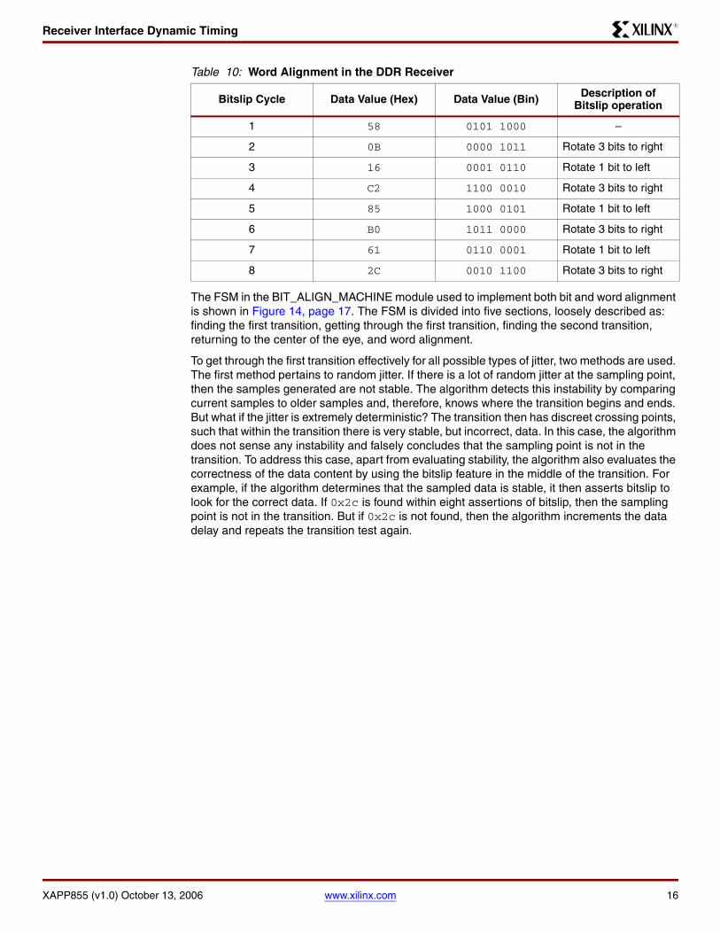
Receiver Interface Dynamic Timing
XAPP855 (v10) October 13 2006 wwwxilinxcom 16
R
The FSM in the BIT_ALIGN_MACHINE module used to implement both bit and word alignment is shown in Figure 14 page 17 The FSM is divided into five sections loosely described as finding the first transition getting through the first transition finding the second transition returning to the center of the eye and word alignment
To get through the first transition effectively for all possible types of jitter two methods are used The first method pertains to random jitter If there is a lot of random jitter at the sampling point then the samples generated are not stable The algorithm detects this instability by comparing current samples to older samples and therefore knows where the transition begins and ends But what if the jitter is extremely deterministic The transition then has discreet crossing points such that within the transition there is very stable but incorrect data In this case the algorithm does not sense any instability and falsely concludes that the sampling point is not in the transition To address this case apart from evaluating stability the algorithm also evaluates the correctness of the data content by using the bitslip feature in the middle of the transition For example if the algorithm determines that the sampled data is stable it then asserts bitslip to look for the correct data If 0x2c is found within eight assertions of bitslip then the sampling point is not in the transition But if 0x2c is not found then the algorithm increments the data delay and repeats the transition test again
Table 10 Word Alignment in the DDR Receiver
Bitslip Cycle Data Value (Hex) Data Value (Bin) Description of Bitslip operation
1 58 0101 1000 ndash
2 0B 0000 1011 Rotate 3 bits to right
3 16 0001 0110 Rotate 1 bit to left
4 C2 1100 0010 Rotate 3 bits to right
5 85 1000 0101 Rotate 1 bit to left
6 B0 1011 0000 Rotate 3 bits to right
7 61 0110 0001 Rotate 1 bit to left
8 2C 0010 1100 Rotate 3 bits to right
Receiver Interface Dynamic Timing
XAPP855 (v10) October 13 2006 wwwxilinxcom 17
R
Figure 14 FSM in the BIT_ALIGN_MACHINE Module
TRANSITION_CHECK (01000)
First TransitionNot Detected
First TransitionNot Detected
First TransitionDetected
First TransitionDetected
Past the FirstTransition
Second TransitionNot Detected
Second TransitionDetected
Decrement DelayAgain
Bit AlignmentComplete
Still Samplingin Transition
INC_ONCE (01111)
SEARCH_PAT (01101)
IDLE (01100)
IDLE (10000)
RECHECK_TRANS (00010)
ONE_BITSLIP (00110)
INC_ONCE (01011)
WAIT_8_CYCLES (00100)
COUNT_1 (01110)
INC_ONCE (01001)
WAIT_8_CYCLES (00011)
IDLE (10010)
TRAINING_DONE (00111)
FIRST_SAMPLE (00001)
RESET (00000)
DEC_TO_HALF (01010)
WORD_ALIGN (00101)
X855_14_082806
Routine to Avoid False Detection of Second Transition
=CHECK_PATTERN
Receiver Interface Dynamic Timing
XAPP855 (v10) October 13 2006 wwwxilinxcom 18
R
Interface Timing Budget
In addition to sampling the data as closely as possible to the center of the data eye the actual size of the data eye is important By accurately predicting the size of the data eye in the receiver the overall performance ceiling of the interface can be inferred The ideal data eye width is the period of the data rate (for example TBit_Period = 100 ns for 1000 Mbs) Both the transmitter and receiver circuits have sources of error that subtract from the ideal data eye The equation for the eye width at the output of the transmitter is shown in Equation 4 TJITTER is the peak-to-peak jitter of the clock source driving the transmitter data bus and forwarded clock TDCD is the maximum duty cycle distortion of the clock tree driving the data bus and forwarded clock Skew is not considered in the transmitter or receiver because the receiver calibrates out skew between channels by performing alignment on each channel individually
Equation 4
Equation 5 calculates the width of the data eye at the receiver flip-flops Ideally the eye width at the receiver is the same as the eye width at the output of the transmitter but there are sources of error in the transmission medium and receiver circuitry Duty cycle distortion must be considered again on the receiver clock tree TSAMP_BUFIO is the receiver sampling error due to drift caused by voltage and temperature variations TIDELAYPAT_JIT is the amount of pattern dependent jitter that is accumulated in each tap of the IDELAY chain For a clock pattern TIDELAYPAT_JIT is 0 pstap peak to peak For a data pattern with long and short run lengths of zeroes and ones (simulated by PRBS23) TIDELAYPAT_JIT is a finite value that must be considered in the timing budget
Equation 5
TBOARD_JITTER includes jitter induced by receiver input capacitance and the parasitics of the physical data path on the PCB TBOARD_JITTER must be determined by simulation as it varies as a function of frequency and for receivers of different types and vendors On the ML550 with a -2 speed-grade Virtex-5 device the TBOARD_JITTER is measured at roughly 200 ps at 900 Mbs (assuming data content equivalent to PRBS23) TQUANTIZATION_ERR or quantization error is caused by the granularity of the IDELAY tap chain Working with 75 ps increments it is not possible to utilize the entire data eye since inevitably some valid eye width is lost between two taps The value for this loss is 75 ps As long as the receiver eye width calculated using Equation 5 is greater than or equal to 0 the interface operates correctly over process voltage and temperature
For example Equation 6 and Equation 7 show the timing budget calculation for the DDR interface running at 900 Mbs in a -2 speed grade device on an ML550 evaluation board Refer to the data sheet for the most current values The TX interface is looped back to the RX interface on the same Virtex-5 FPGA as shown in Equation 2
Equation 6
Equation 7
Changes in voltage and temperature cause the data channels of the interface to drift relative to the clock If the DDR interface were to transfer user data for a long period of time over all specified conditions of temperature and voltage Equation 7 states that there would be at least 107 ps (one or two IDELAY taps) of data window remaining valid during all fluctuations of temperature and voltage Compare this calculation to the measurements in Table 12 page 21 Case 900 Mbs There are four taps that are error free under all conditions In ldquoAppendixrdquo there are three -2 devices tested at 900 Mbs and each has 4 4 and 3 taps respectively that are error free under all conditions
DATA_EYE_WIDTH_TX TBIT_PERIOD TJITTERndash TDCD_BUFIOndash=
DATA_EYE_WIDTH_RX DATA_EYE_WIDTH_TX
TBOARD_JITTER
ndash
TSAMP_BUFIOndash TDCD_BUFIOndash
TIDELAYPAT_JIT IDELAY taps in datapathtimes[ ]ndash
TQUANTIZATION_ERRndash
=
DATA_EYE_WIDTH_TX 1111 ps 25 psndash 100 psndash 986 ps= =
DATA_EYE_WIDTH_RX986 ps 200 psndash 400 psndash 100 psndash 8 ps 13 tapstimes[ ] 75 ps 107 ps=ndashndash
=
Interface Characterization
XAPP855 (v10) October 13 2006 wwwxilinxcom 19
R
At a given temperature and voltage setting the data valid window is much larger because there is no drift when temperature and voltage are constant The size of the data valid window under constant conditions is 107 ps + TSAMP_BUFIO which in this case is at least 507 ps (six or seven IDELAY taps) Compare this calculation to the measurements of any single condition in Table 12 Case 900 Mbs In the worst case (ndash5 supply) there are 7 taps that are error free
Equation 8 and Equation 9 show the same timing budget calculation for the DDR interface running at 10 Gbs in a -2 speed grade device on an ML550 Evaluation Board
Equation 8
Equation 9
Equation 9 predicts that no data window remains valid during all specified fluctuations of temperature and voltage (compare to Table 12 Case 1000 Mbs) In ldquoAppendixrdquo there are three -2 devices tested at 1000 Mbs and each has 1 3 and 1 taps respectively that are error free under all conditions This data rate and device combination are very marginal cases
To operate at 10 Gbs the DDR interface requires additional circuitry to track out voltage-temperature variations in real-time (see XAPP860 16-channel DDR LVDS Interface with Real-time Window Monitoring for a DDR Interface with real-time window monitoring) If the voltage-temperature variations are removed from the picture the predicted data valid window is ndash120 ps + TSAMP_BUFIO which in this case is at least 280 ps (3 or 4 taps) Compare this calculation to the measurements of any single condition in Table 18 page 34 There are at least four error-free taps in all conditions
Interface Characterization
By following the procedure illustrated in Figure 13 page 15 the bit-alignment algorithm should never insert more than approximately 15 bit times of delay on the data channels The fewest number of delay taps should be used in the datapath because they produce a finite amount of degradation (TIDELAYPAT_JIT) The worst-case initial timing for the algorithm occurs when the clock samples just before the data transitions as in the 600 Mbs case in Figure 12 page 14 The algorithm must move all the way through the first eye to find the first transition (1 bit time) and then move halfway into the next eye to center the sampling point (05 bit time) This process produces a worst-case total delay insertion of 15 bit times
The actual performance of the bit-alignment algorithm is characterized as a function of data rate in Figure 15 page 20 For all data rates the expectation is that the tap settings of all 16 channels in the DDR receiver do not exceed approximately 15 bit times of delay Both the maximum and minimum tap setting of all 16 channels is recorded for each data rate This graph only shows the data for a single device Comparing the 15 bit time mask to the actual settings it is clear that the algorithm remains within the 15 bit time limit At 13 Gbs the tap setting actually exceeds the mask by one tap (a negligible violation)
DATA_EYE_WIDTH_TX 1000 ps 25 psndash 100 psndash 875 ps= =
DATA_EYE_WIDTH_RX 875 ps 300 psndash400 ps 100 psndash
ndash8 ps 15 tapstimes[ ] 75 ps 120 psndash=ndashndash
=
Interface Characterization
XAPP855 (v10) October 13 2006 wwwxilinxcom 20
R
The maximum and minimum tap settings in Figure 15 generally stay within 3 to 4 taps of each other except in the case of 640 Mbs and 1300 Mbs data rates These data rates are seams in the inherent timing At data rates below 640 Mbs the tap settings are in the range of 30 taps and at data rates above 640 Mbs the tap settings are in the range of 12 taps Referring back to Figure 12 page 14 it is clear why this seam occurs As the data rate increases past 600 Mbs the initial sampling point of the inherent timing moves into a different data eye creating a different starting point for the algorithm At 640 Mbs some of the 16 channels start in one eye while other channels start in the other eye Fortunately this is not an issue because the single bit time of difference between the channels is resolved using bitslip
Referring back to Figure 8 page 9 the clock channel goes through an IDELAY block with a default value of 0 Once the data rate is chosen for a given design this initial IDELAY value can be changed to a non-zero value to achieve more favorable inherent timing For example a design running at 620 Mbs can use 30 IDELAY taps on the delay channels each contributing a certain amount of jitter to the timing budget calculation By setting the initial clock delay to 5 taps the inherent timing moves across the seam shown in the 600 Mbs range of Figure 15 causing the data channels to only use about 12 IDELAY taps Only spectrally rich data patterns accumulate jitter in the IDELAY tap chain so the clock IDELAY can be set to any value without diminishing the timing budget This optimization is entirely optional and can be done once the design is running in hardware
The DDR receiver is designed to remove skew between channels by aligning each channel individually The ML550 board on which this reference design is characterized is designed to have minimal skew between channels However there is clearly a finite amount of skew between channels due to clock skew in the TX and RX BUFIO networks package skew and trace length tolerance on the ML550 board Table 11 page 21 shows how the bit-alignment algorithm sets the delay for each channel differently to compensate for skew between channels The table captures the range of settings among the 16 channels at specific data rates for a -2 device If there were additional skew among the 16 channels then the tap setting range would be larger to compensate for it The algorithm is designed such that skew between channels should not diminish the performance of the interface The range of tap settings differs for different devices and speed grades but the magnitude should be approximately the same
Figure 15 Bit-Alignment Algorithm Performance
60
50
40
30
20
10
0200 400 600 800 1000 1200 1400 1600
Data Rate (Mbs)
Del
ay T
ap U
tiliz
atio
n HW Measurement (Min)HW Measurement (Max)15 Bit Time Mask
X855_15_072406
Interface Characterization
XAPP855 (v10) October 13 2006 wwwxilinxcom 21
R
Since the receiver alignment logic only runs once immediately after reset the resulting dynamic timing must be adequate to ensure error-free operation over the specified voltage and temperature variations that can occur over time The data-valid window at the receiver input must be wide enough to withstand these variations (receiver drift) Table 12 page 21 shows the data-valid window at the ISERDES registers in the DDR receiver The eyes shown are collective eyes of all 16 channels The BERT testbench configuration loops back the DDR transmitter to the DDR receiver Using pattern generators and error detectors programmed to send and receive a pseudorandom bit sequence (PRBS23) the width of the data-valid window is evaluated using pseudorandom data that closely resembles real user data
Table 11 Tap Setting Range For Various Data Rates Measured on a -2 Device
Data Rate (Mbs) Tap Setting Range Compensated Skew
500 31ndash34 4 taps
600 28ndash30 3 taps
700 10ndash12 3 taps
800 11ndash13 3 taps
900 11ndash13 3 taps
1000 13ndash15 3 taps
1100 13ndash15 3 taps
1200 14ndash15 2 taps
Table 12 Measurement of Receiver Drift under Extreme Conditions for Multiple Data Rates
ConditionIODELAY Taps (1)
ndash8 ndash7 ndash6 ndash5 ndash4 ndash3 ndash2 ndash1 0 +1 +2 +3 +4 +5 +6 +7 +8
Case 800 Mbs
25degC Nom Supplies F F F P P P P P C P P P P P F F F
0degC Nom Supplies F F F P P P P P P P P P P P F F F
85degC Nom Supplies F F F P P P P P P P P P P P F F F
25degC +5 Supplies F P P P P P P P P P P P F F F F F
0degC +5 Supplies F P P P P P P P P P P P F F F F F
85degC +5 Supplies F P P P P P P P P P P P F F F F F
25degC ndash5 Supplies F F F F F F P P P P P P P P P F F
0degC ndash5 Supplies F F F F F F P P P P P P P P P P F
85degC ndash5 Supplies F F F F F P P P P P P P P P P F F
CONCLUSION Error free under all conditions when calibrated under nominal conditions to position C
Interface Characterization
XAPP855 (v10) October 13 2006 wwwxilinxcom 22
R
Case 900 Mbs
25degC Nom Supplies F F F F P P P P C P P P P F F F F
0degC Nom Supplies F F F F P P P P P P P P P F F F F
85degC Nom Supplies F F F F P P P P P P P P F F F F F
25degC +5 Supplies F F P P P P P P P P P F F F F F F
0degC +5 Supplies F F P P P P P P P P P F F F F F F
85degC +5 Supplies F F P P P P P P P P P F F F F F F
25degC ndash5 Supplies F F F F F F F P P P P P P P P F F
0degC ndash5 Supplies F F F F F F F P P P P P P P P F F
85degC ndash5 Supplies F F F F F F F P P P P P P P F F F
CONCLUSION Error free under all conditions when calibrated under nominal conditions to position C
Case 1000 Mbs
25degC Nom Supplies F F F F F P P P C P P P F F F F F
0degC Nom Supplies F F F F F P P P P P P P F F F F F
85degC Nom Supplies F F F F F P P P P P P P F F F F F
25degC +5 Supplies F F F P P P P P P P F F F F F F F
0degC +5 Supplies F F F P P P P P P P F F F F F F F
85degC +5 Supplies F F F P P P P P P P P F F F F F F
25degC ndash5 Supplies F F F F F F F F P P P P P P F F F
0degC ndash5 Supplies F F F F F F F F P P P P P P F F F
85degC ndash5 Supplies F F F F F F F F P P P P P P F F F
CONCLUSION Error free under all conditions when calibrated under nominal conditions to position C
Case 1100 Mbs
25degC Nom Supplies F F F F F P P P C P F F F F F F F
0degC Nom Supplies F F F F F P P P P P F F F F F F F
85degC Nom Supplies F F F F F P P P P P F F F F F F F
25degC +5 Supplies F F F P P P P P P F F F F F F F F
0degC +5 Supplies F F F P P P P P P F F F F F F F F
85degC +5 Supplies F F F P P P P P P F F F F F F F F
25degC ndash5 Supplies F F F F F F F F P P P P F F F F F
0degC ndash5 Supplies F F F F F F F F P P P P F F F F F
85degC ndash5 Supplies F F F F F F F F P P P P F F F F F
CONCLUSION Error free under all conditions when calibrated under nominal conditions to position C
Table 12 Measurement of Receiver Drift under Extreme Conditions for Multiple Data Rates (Continued)
ConditionIODELAY Taps (1)
ndash8 ndash7 ndash6 ndash5 ndash4 ndash3 ndash2 ndash1 0 +1 +2 +3 +4 +5 +6 +7 +8
Interface Characterization
XAPP855 (v10) October 13 2006 wwwxilinxcom 23
R
In all test cases shown in Table 12 page 21 the bit-align machine accurately places the sampling point in the center of the data eye (indicated by the C in each test case) In the 1100 Mbs case the bit-align machine places the sampling point slightly off center This slight inaccuracy occurs when the center of a real data pattern diverges from the center of the training pattern The electrical behavior of different data patterns is discussed below
After the dynamic timing is established for a given test case under nominal conditions the device is subjected to extremes of temperature and voltage to stress the receiver timing At data rates of 1100 Mbs and below the dynamic timing established after reset under nominal conditions is sufficient to meet timing over all specified extreme conditions (the column with the C passes traffic error free under all conditions) At a data rate of 1200 Mbs the design operates correctly under nominal conditions but the data-valid window is not large enough to withstand the voltage variations For this particular transmission medium the 1200 Mbs case requires a real-time adjustment circuit that could track the center of the eye
The full datapath of the testbench consists of
TX rarr 5 FR-4 rarr SAMTEC QSE Conn rarr 12 Ribbon Cable rarr SAMTEC QSE Conn rarr 5 FR-4 rarr RX
For shorter transmission media higher performance can be achieved in accordance with the section ldquoInterface Timing Budgetrdquo page 18 Interface performance is not solely a question of the LVDS driver performance specification but rather a question of adequate timing margin to withstand production and environmental variations From Table 12 the total amount of variation experienced over temperature and voltage is roughly 375 ps (5 taps at 75 ps per tap) This number should be comparable to the specification for receiver sampling error (TSAMP_BUFIO) shown in the Virtex-5 Data Sheet
Case 1200 Mbs
25degC Nom Supplies F F F F F F P P C P F F F F F F F
0degC Nom Supplies F F F F F F P P P P F F F F F F F
85degC Nom Supplies F F F F F F P P P F F F F F F F F
25degC +5 Supplies F F F F P P P P F F F F F F F F F
0degC +5 Supplies F F F P P P P P F F F F F F F F F
85degC +5 Supplies F F F F P P P P F F F F F F F F F
25degC ndash5 Supplies F F F F F F F F F P P P F F F F F
0degC ndash5 Supplies F F F F F F F F F P P P F F F F F
85degC ndash5 Supplies F F F F F F F F F P P F F F F F F
CONCLUSION Errors caused by plusmn5 variations in supply voltages
Notes 1 Where 0 is the reference tap determined by the bit-align machine under nominal conditions at 25degC2 P = Error-free transmission F = Error in transmission C = IODELAY tap position selected by bit-align machine under nominal conditions at 25degC3 Device under test is -2 speed grade
Table 12 Measurement of Receiver Drift under Extreme Conditions for Multiple Data Rates (Continued)
ConditionIODELAY Taps (1)
ndash8 ndash7 ndash6 ndash5 ndash4 ndash3 ndash2 ndash1 0 +1 +2 +3 +4 +5 +6 +7 +8
Interface Characterization
XAPP855 (v10) October 13 2006 wwwxilinxcom 24
R
Pattern Dependence of Receiver Performance
Different types of data patterns have different electrical signatures (rise and fall times jitter eye symmetry etc) A pattern with very narrow spectral content (such as a clock pattern) moves very favorably through the link because the receiver frequency response has little effect on the signal integrity However a pattern with wide spectral content (such as real data and pseudorandom patterns) stresses the links frequency response If the frequency response is not flat across the entire spectrum of the data content then the signal integrity is degraded as a result The amount of degradation measured is shown in Table 13 page 25 The DDR transmitter is looped back to the DDR receiver and different patterns are programmed to traverse the link Performance is assessed by evaluating the integrity of those patterns in the receiver
PRBS7 is a pseudorandom data pattern with a maximum run length of seven consecutive zeroes or ones PRBS15 is defined as having a maximum run length of fifteen consecutive zeroes or ones These limitations on run lengths limit the spectral content of the pattern A PRBS15 pattern has greater spectral content than a PRBS7 pattern and therefore is a more strenuous test for the link PRBS29 is the most strenuous test in Table 13 A clock pattern is effectively a PRBS1
As predicted Table 13 shows that there is more degradation for data patterns with more spectral content At 1000 Mbs and below the data eye closure is symmetrical Symmetrical eye closure is desired because it does not change the center of the eye as determined by the bit-alignment algorithm Above 1000 Mbs the eye closure becomes more asymmetrical causing the center of the data eye to diverge from the calibrated center (by only 1 tap)
In every data rate shown in Table 13 all significant pattern-dependent degradation is caused between PRBS1 (clock pat) and PRBS15 Between PRBS15 and PRBS29 there is no additional degradation recorded in any of the measurements
Interface Characterization
XAPP855 (v10) October 13 2006 wwwxilinxcom 25
R
Table 13 Link Performance for Various Types of Data Measured on a -2 Device
PatternIODELAY Taps (1)
ndash8 ndash7 ndash6 ndash5 ndash4 ndash3 ndash2 ndash1 0 +1 +2 +3 +4 +5 +6 +7 +8 +9
Case 600 Mbs
Clock Pat (0101) P P P P P P P P C P P P P P P P P P
Training Pat (0x2C) P P P P P P P P C P P P P P P P P F
PRBS7 P P P P P P P P C P P P P P P P P F
PRBS15 F P P P P P P P C P P P P P P P F F
PRBS23 F P P P P P P P C P P P P P P P F F
PRBS29 F P P P P P P P C P P P P P P P F F
Case 800 Mbs
Clock Pat (0101) F F P P P P P P C P P P P P P F F F
Training Pat (0x2C) F F P P P P P P C P P P P P P F F F
PRBS7 F F P P P P P P C P P P P P F F F F
PRBS15 F F F P P P P P C P P P P P F F F F
PRBS23 F F F P P P P P C P P P P P F F F F
PRBS29 F F F P P P P P C P P P P P F F F F
Case 1000 Mbs
Clock Pat (0101) F F F P P P P P C P P P P P F F F F
Training Pat (0x2C) F F F P P P P P C P P P P F F F F F
PRBS7 F F F F P P P P C P P P F F F F F F
PRBS15 F F F F F P P P C P P P F F F F F F
PRBS23 F F F F F P P P C P P P F F F F F F
PRBS29 F F F F F P P P C P P P F F F F F F
Case 1200 Mbs
Clock Pat (0101) F F F F P P P P C P P P P F F F F F
Training Pat (0x2C) F F F F P P P P C P P P F F F F F F
PRBS7 F F F F F P P P C P F F F F F F F F
PRBS15 F F F F F F P P C F F F F F F F F F
PRBS23 F F F F F F P P C F F F F F F F F F
PRBS29 F F F F F F P P C F F F F F F F F F
Case 1400 Mbs
Clock Pat (0101) F F F F F F P P C P P P F F F F F F
Training Pat (0x2C) F F F F F P P P C P P F F F F F F F
PRBS7 F F F F F F F P C P F F F F F F F F
PRBS15 F F F F F F F P C F F F F F F F F F
PRBS23 F F F F F F F P C F F F F F F F F F
PRBS29 F F F F F F F P C F F F F F F F F F
Notes 1 Where 0 is the reference tap determined by the bit-align machine under nominal conditions at 25degC2 P = Error-free transmission F = Error in transmission C = IODELAY tap position selected by bit-align machine under nominal conditions at 25degC
Resetting the Interface
XAPP855 (v10) October 13 2006 wwwxilinxcom 26
R
Resetting the Interface
Several dependencies determine the order in which circuits should be reset in the interface The receiver cannot begin the alignment algorithm if the transmitter is not sending the training pattern The transmitter must be reset before the receiver and time must be allowed for the training pattern to propagate across the link before the receiver comes out of reset The receiver also cannot begin the alignment algorithm until IDELAYCTRL has recovered from reset which could takes hundreds of cycles The recommended reset timing for the interface is shown in Figure 16 This reset timing is implemented in the BERT testbench for this interface
The TX reset (RST_TX) is used to reset all TX circuitry and also IDELAYCTRL The IDELAYCTRL reset is asynchronous so driving it with RST_TX is acceptable The minimum pulse width of IDELAYCTRL reset is 50 ns (TIDELAYCTRL_RPW) For that reason resets are held High for 16 clock cycles The RX reset (RST_RX) is used to reset all RX circuitry and is asserted when the IDELAYCTRL READY flag goes High indicating that the IODELAY blocks are calibrated
The timing of the READY flag in Figure 16 is a potential hazard Most likely it is High during a TX reset because it takes many cycles for IDELAYCTRL to deassert the READY flag It is easy to make the mistake of resetting the receiver too early To avoid this hazard the RX reset should be asserted only after seeing a deassertion and reassertion of the READY flag
Conclusion Based on the design and characterization described in this document the 16-Channel DDR reference design operates to the performance targets in Table 14 under all conditions of process voltage and temperature However to meet these targets over voltage and temperature the timing budget must be guaranteed according to the analysis in ldquoInterface Timing Budgetrdquo See ldquoAppendixrdquo page 27 for further justification of the maximum performance recommendations in Table 14
Figure 16 Recommended Interface Reset Timing
RST_TX
IDELAYCTRLREADY
RST_RX
16 Cycles X855_16_072406
Table 14 Performance of 16-Channel DDR Interface
Speed Grade Maximum Performance
-1 800 Mbs
-2 900 Mbs
-3 10 Gbs(1)
Notes 1 To achieve higher performance (up to 125 Gbs) see 16-channel DDR LVDS Interface with Realtime
Window Monitoring for an example of a DDR interface with real-time window monitoring
Appendix
XAPP855 (v10) October 13 2006 wwwxilinxcom 27
R
Appendix Performance Characterization Data
Refer to ldquoInterface Characterizationrdquo page 19 for explanations about how to interpret the data in the ldquoAppendixrdquo These tables show collective data eyes for the entire interface over process voltage and temperature (PVT) Three devices from each speed grade were selected for this characterization
The calibrated center position of the eye (marked by the C in the tables below) varies slightly from channel to channel (due to small skews between channels) That range is referred to as center tap range Analysis of Table 16 page 28 through Table 20 page 40 shows that the center tap range for slow and fast parts differ significantly at the same data rate (because the BIT_ALIGN_MACHINE algorithm adjusts for differences in speed)
All data in the ldquoAppendixrdquo is collected using the BERT testbench shown in Figure 2 page 2 The data pattern is PRBS23 and the devicepackage is XC5VLX50T-FF1136 The transmission path for the cases shown in Table 16 through Table 20 is repeated for convenience
TX rarr 5 FR-4 rarr SAMTEC QSE Conn rarr 12 Ribbon Cable rarr SAMTEC QSE Conn rarr 5 FR-4 rarr RX
A summary of these characterization results is shown in Table 15 Each of the nine parts were tested at 800 900 1000 1100 and 1200 Mbs When the interface is error free on all channels under all extreme conditions of temperature and voltage the particular test case is designated by a P A test case is marked FAIL when the interface suffered errors on any channel under any particular condition of voltage and temperature
Table 15 Summary of Interface Characterization Results
Device (SN) Speed Grade 800 Mbs 900 Mbs 1000Mbs 1100 Mbs 1200 Mbs
2194 -1 P P P FAIL FAIL
2219 -1 P FAIL FAIL FAIL FAIL
2199 -1 P P FAIL FAIL FAIL
001 -2 P P FAIL P FAIL
002 -2 P P P P FAIL
003 -2 P P FAIL FAIL FAIL
004 -3 P P P P P
005 -3 P P P P P
006 -3 P P P P P
Appendix
XAPP855 (v10) October 13 2006 wwwxilinxcom 28
R
Table 16 Measurement of Receiver Drift under Extreme Conditions at 800 Mbs
ConditionIODELAY Taps (1)
ndash8 ndash7 ndash6 ndash5 ndash4 ndash3 ndash2 ndash1 0 +1 +2 +3 +4 +5 +6 +7 +8
SN 2194 Speed Grade -1
25degC Nom Supplies F F F P P P P P C P P P P F F F F
0degC Nom Supplies F F F P P P P P P P P P P F F F F
85degC Nom Supplies F F F F P P P P P P P P P F F F F
25degC +5 Supplies F F P P P P P P P P P P F F F F F
0degC +5 Supplies F F P P P P P P P P P P F F F F F
85degC +5 Supplies F F P P P P P P P P P P F F F F F
25degC ndash5 Supplies F F F F F F P P P P P P P P P F F
0degC ndash5 Supplies F F F F F F P P P P P P P P P F F
85degC ndash5 Supplies F F F F F F P P P P P P P P P F F
Center Tap Range Taps 11ndash12
CONCLUSION Error free under all conditions when calibrated under nominal conditions to position C
SN 2219 Speed Grade -1
25degC Nom Supplies F F F P P P P P C P P P F F F F F
0degC Nom Supplies F F F P P P P P P P P P F F F F F
85degC Nom Supplies F F F P P P P P P P P P F F F F F
25degC +5 Supplies F P P P P P P P P P P F F F F F F
0degC +5 Supplies F P P P P P P P P P P F F F F F F
85degC +5 Supplies F P P P P P P P P P P F F F F F F
25degC ndash5 Supplies F F F F F F P P P P P P P P F F F
0degC ndash5 Supplies F F F F F F F P P P P P P P F F F
85degC ndash5 Supplies F F F F F F P P P P P P P P F F F
Center Tap Range Taps 13ndash16
CONCLUSION Error free under all conditions when calibrated under nominal conditions to position C
SN 2199 Speed Grade -1
25degC Nom Supplies F F F P P P P P C P P P P F F F F
0degC Nom Supplies F F F P P P P P P P P P P F F F F
85degC Nom Supplies F F F P P P P P P P P P P F F F F
25degC +5 Supplies F P P P P P P P P P P P F F F F F
0degC +5 Supplies F P P P P P P P P P P P F F F F F
85degC +5 Supplies F P P P P P P P P P P P F F F F F
25degC ndash5 Supplies F F F F F F P P P P P P P P P F F
0degC ndash5 Supplies F F F F F F P P P P P P P P P F F
85degC ndash5 Supplies F F F F F F P P P P P P P P P F F
Center Tap Range Taps 10ndash12
CONCLUSION Error free under all conditions when calibrated under nominal conditions to position C
Appendix
XAPP855 (v10) October 13 2006 wwwxilinxcom 29
R
SN 001 Speed Grade -2
25degC Nom Supplies F F F P P P P P C P P P P F F F F
0degC Nom Supplies F F F P P P P P P P P P P F F F F
85degC Nom Supplies F F F P P P P P P P P P P F F F F
25degC +5 Supplies F P P P P P P P P P P P F F F F F
0degC +5 Supplies F P P P P P P P P P P F F F F F F
85degC +5 Supplies F P P P P P P P P P P P F F F F F
25degC ndash5 Supplies F F F F F P P P P P P P P P P F F
0degC ndash5 Supplies F F F F F P P P P P P P P P P F F
85degC ndash5 Supplies F F F F F P P P P P P P P P P F F
Center Tap Range Taps 10ndash12
CONCLUSION Error free under all conditions when calibrated under nominal conditions to position C
SN 002 Speed Grade -2
25degC Nom Supplies F F F P P P P P C P P P P F F F F
0degC Nom Supplies F F F P P P P P P P P P P F F F F
85degC Nom Supplies F F F P P P P P P P P P P F F F F
25degC +5 Supplies F P P P P P P P P P P P F F F F F
0degC +5 Supplies F P P P P P P P P P P P F F F F F
85degC +5 Supplies F F P P P P P P P P P P F F F F F
25degC ndash5 Supplies F F F F F P P P P P P P P P P F F
0degC ndash5 Supplies F F F F F P P P P P P P P P P F F
85degC ndash5 Supplies F F F F F P P P P P P P P P P F F
Center Tap Range Taps 10ndash12
CONCLUSION Error free under all conditions when calibrated under nominal conditions to position C
SN 003 Speed Grade -2
25degC Nom Supplies F F F P P P P P C P P P P F F F F
0degC Nom Supplies F F F P P P P P P P P P P F F F F
85degC Nom Supplies F F F P P P P P P P P P P F F F F
25degC +5 Supplies F P P P P P P P P P P P F F F F F
0degC +5 Supplies F P P P P P P P P P P F F F F F F
85degC +5 Supplies F P P P P P P P P P P P F F F F F
25degC ndash5 Supplies F F F F F F P P P P P P P P P F F
0degC ndash5 Supplies F F F F F F P P P P P P P P P F F
85degC ndash5 Supplies F F F F F F P P P P P P P P P F F
Center Tap Range Taps 11ndash13
CONCLUSION Error free under all conditions when calibrated under nominal conditions to position C
Table 16 Measurement of Receiver Drift under Extreme Conditions at 800 Mbs (Continued)
ConditionIODELAY Taps (1)
ndash8 ndash7 ndash6 ndash5 ndash4 ndash3 ndash2 ndash1 0 +1 +2 +3 +4 +5 +6 +7 +8
Appendix
XAPP855 (v10) October 13 2006 wwwxilinxcom 30
R
SN 004 Speed Grade -3
25degC Nom Supplies F F F P P P P P C P P P P F F F F
0degC Nom Supplies F F F P P P P P P P P P F F F F F
85degC Nom Supplies F F F P P P P P P P P P P F F F F
25degC +5 Supplies F P P P P P P P P P P P F F F F F
0degC +5 Supplies F P P P P P P P P P P P F F F F F
85degC +5 Supplies F F P P P P P P P P P P F F F F F
25degC ndash5 Supplies F F F F F P P P P P P P P P F F F
0degC ndash5 Supplies F F F F F P P P P P P P P P F F F
85degC ndash5 Supplies F F F F F P P P P P P P P P F F F
Center Tap Range Taps 8ndash9 23ndash24
CONCLUSION Error free under all conditions when calibrated under nominal conditions to position C
SN 005 Speed Grade -3
25degC Nom Supplies F F P P P P P P C P P P P F F F F
0degC Nom Supplies F F P P P P P P P P P P P F F F F
85degC Nom Supplies F F F P P P P P P P P P P P F F F
25degC +5 Supplies F P P P P P P P P P P P F F F F F
0degC +5 Supplies F P P P P P P P P P P P F F F F F
85degC +5 Supplies F P P P P P P P P P P P F F F F F
25degC ndash5 Supplies F F F F P P P P P P P P P P P F F
0degC ndash5 Supplies F F F F P P P P P P P P P P P F F
85degC ndash5 Supplies F F F F P P P P P P P P P P P F F
Center Tap Range Taps 9ndash10
CONCLUSION Error free under all conditions when calibrated under nominal conditions to position C
SN 006 Speed Grade -3
25degC Nom Supplies F F P P P P P P C P P P P F F F F
0degC Nom Supplies F F P P P P P P P P P P P F F F F
85degC Nom Supplies F F F P P P P P P P P P P F F F F
25degC +5 Supplies F P P P P P P P P P P P F F F F F
0degC +5 Supplies F P P P P P P P P P P P F F F F F
85degC +5 Supplies F F P P P P P P P P P P F F F F F
25degC ndash5 Supplies F F F P P P P P P P P P P P F F F
0degC ndash5 Supplies F F F P P P P P P P P P P P F F F
85degC ndash5 Supplies F F F F F P P P P P P P P P F F F
Center Tap Range Taps 8ndash9 23ndash24
CONCLUSION Error free under all conditions when calibrated under nominal conditions to position C
Notes 1 IODELAY taps where 0 is the reference tap determined by the bit align machine at nominal voltage and 25degC2 P = Error-free transmission F = Error in transmission C = IODELAY tap position selected by bit-align machine under nominal conditions at 25degC
Table 16 Measurement of Receiver Drift under Extreme Conditions at 800 Mbs (Continued)
ConditionIODELAY Taps (1)
ndash8 ndash7 ndash6 ndash5 ndash4 ndash3 ndash2 ndash1 0 +1 +2 +3 +4 +5 +6 +7 +8
Appendix
XAPP855 (v10) October 13 2006 wwwxilinxcom 31
R
Table 17 Measurement of Receiver Drift under Extreme Conditions at 900 Mbs
ConditionIODELAY Taps (1)
ndash8 ndash7 ndash6 ndash5 ndash4 ndash3 ndash2 ndash1 0 +1 +2 +3 +4 +5 +6 +7 +8
SN 2194 Speed Grade -1
25degC Nom Supplies F F F F F P P P C P P P F F F F F
0degC Nom Supplies F F F F F P P P P P P P F F F F F
85degC Nom Supplies F F F F F P P P P P P P P F F F F
25degC +5 Supplies F F F P P P P P P P P F F F F F F
0degC +5 Supplies F F F P P P P P P P P F F F F F F
85degC +5 Supplies F F F P P P P P P P P F F F F F F
25degC ndash5 Supplies F F F F F F F P P P P P P P F F F
0degC ndash5 Supplies F F F F F F F P P P P P P P F F F
85degC ndash5 Supplies F F F F F F F P P P P P P P F F F
Center Tap Range Taps 11ndash12
CONCLUSION Error free under all conditions when calibrated under nominal conditions to position C
SN 2219 Speed Grade -1
25degC Nom Supplies F F F F F P P P C P P P F F F F F
0degC Nom Supplies F F F F F P P P P P P P F F F F F
85degC Nom Supplies F F F F F P P P P P P P F F F F F
25degC +5 Supplies F F F P P P P P P P F F F F F F F
0degC +5 Supplies F F F P P P P P P P F F F F F F F
85degC +5 Supplies F F F P P P P P P P F F F F F F F
25degC ndash5 Supplies F F F F F F F F F P P P P P F F F
0degC ndash5 Supplies F F F F F F F F F P P P P P F F F
85degC ndash5 Supplies F F F F F F F F P P P P P P F F F
Center Tap Range Taps 12ndash15
CONCLUSION Errors caused by ndash5 variation in supply voltage
SN 2199 Speed Grade -1
25degC Nom Supplies F F F F F P P P C P P P F F F F F
0degC Nom Supplies F F F F F P P P P P P P F F F F F
85degC Nom Supplies F F F F F P P P P P P P F F F F F
25degC +5 Supplies F F F P P P P P P P P F F F F F F
0degC +5 Supplies F F F P P P P P P P P F F F F F F
85degC +5 Supplies F F F P P P P P P P P F F F F F F
25degC ndash5 Supplies F F F F F F F F P P P P P P F F F
0degC ndash5 Supplies F F F F F F F F P P P P P P F F F
85degC ndash5 Supplies F F F F F F F F P P P P P P F F F
Center Tap Range Taps 10ndash12
CONCLUSION Error free under all conditions when calibrated under nominal conditions to position C
Appendix
XAPP855 (v10) October 13 2006 wwwxilinxcom 32
R
SN 001 Speed Grade -2
25degC Nom Supplies F F F F P P P P C P P P P F F F F
0degC Nom Supplies F F F F P P P P P P P P P F F F F
85degC Nom Supplies F F F F F P P P P P P P P F F F F
25degC +5 Supplies F F P P P P P P P P P F F F F F F
0degC +5 Supplies F F P P P P P P P P P F F F F F F
85degC +5 Supplies F F F P P P P P P P P P F F F F F
25degC ndash5 Supplies F F F F F F F P P P P P P P F F F
0degC ndash5 Supplies F F F F F F F P P P P P P P F F F
85degC ndash5 Supplies F F F F F F F P P P P P P P F F F
Center Tap Range Taps 9ndash11
CONCLUSION Error free under all conditions when calibrated under nominal conditions to position C
SN 002 Speed Grade -2
25degC Nom Supplies F F F F P P P P C P P P P F F F F
0degC Nom Supplies F F F F P P P P P P P P F F F F F
85degC Nom Supplies F F F F F P P P P P P P P F F F F
25degC +5 Supplies F F F P P P P P P P P F F F F F F
0degC +5 Supplies F F F P P P P P P P P F F F F F F
85degC +5 Supplies F F F P P P P P P P P P F F F F F
25degC ndash5 Supplies F F F F F F F P P P P P P P F F F
0degC ndash5 Supplies F F F F F F F P P P P P P P F F F
85degC ndash5 Supplies F F F F F F F P P P P P P P F F F
Center Tap Range Taps 10ndash12
CONCLUSION Error free under all conditions when calibrated under nominal conditions to position C
SN 003 Speed Grade -2
25degC Nom Supplies F F F F F P P P C P P P P F F F F
0degC Nom Supplies F F F F F P P P P P P P P F F F F
85degC Nom Supplies F F F F F P P P P P P P P F F F F
25degC +5 Supplies F F P P P P P P P P P F F F F F F
0degC +5 Supplies F F P P P P P P P P P F F F F F F
85degC +5 Supplies F F F P P P P P P P P F F F F F F
25degC ndash5 Supplies F F F F F F F P P P P P P P F F F
0degC ndash5 Supplies F F F F F F F F P P P P P P F F F
85degC ndash5 Supplies F F F F F F F P P P P P P P F F F
Center Tap Range Taps 11ndash13
CONCLUSION Error free under all conditions when calibrated under nominal conditions to position C
Table 17 Measurement of Receiver Drift under Extreme Conditions at 900 Mbs (Continued)
ConditionIODELAY Taps (1)
ndash8 ndash7 ndash6 ndash5 ndash4 ndash3 ndash2 ndash1 0 +1 +2 +3 +4 +5 +6 +7 +8
Appendix
XAPP855 (v10) October 13 2006 wwwxilinxcom 33
R
SN 004 Speed Grade -3
25degC Nom Supplies F F F F P P P P C P P P P F F F F
0degC Nom Supplies F F F P P P P P P P P P P F F F F
85degC Nom Supplies F F F F P P P P P P P P P F F F F
25degC +5 Supplies F F F P P P P P P P P P F F F F F
0degC +5 Supplies F F F P P P P P P P P P F F F F F
85degC +5 Supplies F F F P P P P P P P P P F F F F F
25degC ndash5 Supplies F F F F F F P P P P P P P P F F F
0degC ndash5 Supplies F F F F F F P P P P P P P P F F F
85degC ndash5 Supplies F F F F F F P P P P P P P P F F F
Center Tap Range Taps 7ndash8
CONCLUSION Error free under all conditions when calibrated under nominal conditions to position C
SN 005 Speed Grade ndash3
25degC Nom Supplies F F F P P P P P C P P P P F F F F
0degC Nom Supplies F F F P P P P P P P P P P F F F F
85degC Nom Supplies F F F F P P P P P P P P P F F F F
25degC +5 Supplies F F P P P P P P P P P P F F F F F
0degC +5 Supplies F F P P P P P P P P P P F F F F F
85degC +5 Supplies F F F P P P P P P P P P F F F F F
25degC ndash5 Supplies F F F F F F P P P P P P P P F F F
0degC ndash5 Supplies F F F F F P P P P P P P P P F F F
85degC ndash5 Supplies F F F F F F P P P P P P P P F F F
Center Tap Range Taps 9ndash10
CONCLUSION Error free under all conditions when calibrated under nominal conditions to position C
SN 006 Speed Grade -3
25degC Nom Supplies F F F F P P P P C P P P P F F F F
0degC Nom Supplies F F F F P P P P P P P P P F F F F
85degC Nom Supplies F F F F P P P P P P P P P F F F F
25degC +5 Supplies F F P P P P P P P P P P F F F F F
0degC +5 Supplies F F P P P P P P P P P P F F F F F
85degC +5 Supplies F F F P P P P P P P P P F F F F F
25degC ndash5 Supplies F F F F F P P P P P P P P P F F F
0degC ndash5 Supplies F F F F F P P P P P P P P P F F F
85degC ndash5 Supplies F F F F F F P P P P P P P P F F F
Center Tap Range Taps 7ndash8
CONCLUSION Error free under all conditions when calibrated under nominal conditions to position C
Notes 1 IODELAY taps where 0 is the reference tap determined by the bit align machine at nominal voltage and 25degC2 P = Error-free transmission F = Error in transmission C = IODELAY tap position selected by bit-align machine under nominal conditions at 25degC
Table 17 Measurement of Receiver Drift under Extreme Conditions at 900 Mbs (Continued)
ConditionIODELAY Taps (1)
ndash8 ndash7 ndash6 ndash5 ndash4 ndash3 ndash2 ndash1 0 +1 +2 +3 +4 +5 +6 +7 +8
Appendix
XAPP855 (v10) October 13 2006 wwwxilinxcom 34
R
Table 18 Measurement of Receiver Drift under Extreme Conditions at 1000 Mbs
ConditionIODELAY Taps (1)
ndash8 ndash7 ndash6 ndash5 ndash4 ndash3 ndash2 ndash1 0 +1 +2 +3 +4 +5 +6 +7 +8
SN 2194 Speed Grade -1
25degC Nom Supplies F F F F F P P P C P P F F F F F F
0degC Nom Supplies F F F F F P P P P P P F F F F F F
85degC Nom Supplies F F F F F P P P P P P F F F F F F
25degC +5 Supplies F F F P P P P P P P F F F F F F F
0degC +5 Supplies F F F P P P P P P P F F F F F F F
85degC +5 Supplies F F F F P P P P P P F F F F F F F
25degC ndash5 Supplies F F F F F F F F P P P P P F F F F
0degC ndash5 Supplies F F F F F F F F P P P P P F F F F
85degC ndash5 Supplies F F F F F F F F P P P P P F F F F
Center Tap Range Taps 12ndash13
CONCLUSION Error free under all conditions when calibrated under nominal conditions to position C
SN 2219 Speed Grade -1
25degC Nom Supplies F F F F F F P P C P P F F F F F F
0degC Nom Supplies F F F F F F P P P P P F F F F F F
85degC Nom Supplies F F F F F F P P P P P F F F F F F
25degC +5 Supplies F F F P P P P P P F F F F F F F F
0degC +5 Supplies F F F P P P P P P F F F F F F F F
85degC +5 Supplies F F F F P P P P P F F F F F F F F
25degC ndash5 Supplies F F F F F F F F F P P P P F F F F
0degC ndash5 Supplies F F F F F F F F F F P P P F F F F
85degC ndash5 Supplies F F F F F F F F F P P P P F F F F
Center Tap Range Taps 14ndash17
CONCLUSION Errors caused by ndash5 variation in supply voltage
SN 2199 Speed Grade -1
25degC Nom Supplies F F F F F F P P C P P F F F F F F
0degC Nom Supplies F F F F F F P P P P P F F F F F F
85degC Nom Supplies F F F F F F P P P P P F F F F F F
25degC +5 Supplies F F F F P P P P P P F F F F F F F
0degC +5 Supplies F F F F P P P P P P F F F F F F F
85degC +5 Supplies F F F F P P P P P P F F F F F F F
25degC ndash5 Supplies F F F F F F F F F P P P P F F F F
0degC ndash5 Supplies F F F F F F F F F P P P P F F F F
85degC ndash5 Supplies F F F F F F F F F P P P P F F F F
Center Tap Range Taps 12ndash14
CONCLUSION Errors caused by ndash5 variation in supply voltage
Appendix
XAPP855 (v10) October 13 2006 wwwxilinxcom 35
R
SN 001 Speed Grade -2
25degC Nom Supplies F F F F F F P P C P P P F F F F F
0degC Nom Supplies F F F F F F P P P P P P F F F F F
85degC Nom Supplies F F F F F F P P P P P P F F F F F
25degC +5 Supplies F F F F P P P P P P F F F F F F F
0degC +5 Supplies F F F F P P P P P P F F F F F F F
85degC +5 Supplies F F F F P P P P P P P F F F F F F
25degC ndash5 Supplies F F F F F F F F F P P P P F F F F
0degC ndash5 Supplies F F F F F F F F F P P P P F F F F
85degC ndash5 Supplies F F F F F F F F F P P P P F F F F
Center Tap Range Taps 11ndash12
CONCLUSION Errors caused by ndash5 variation in supply voltage
SN 002 Speed Grade -2
25degC Nom Supplies F F F F F P P P C P P F F F F F F
0degC Nom Supplies F F F F F P P P P P P P F F F F F
85degC Nom Supplies F F F F F P P P P P P P F F F F F
25degC +5 Supplies F F F F P P P P P P F F F F F F F
0degC +5 Supplies F F F P P P P P P P F F F F F F F
85degC +5 Supplies F F F F P P P P P P P F F F F F F
25degC ndash5 Supplies F F F F F F F P P P P P P F F F F
0degC ndash5 Supplies F F F F F F F P P P P P P F F F F
85degC ndash5 Supplies F F F F F F F P P P P P P F F F F
Center Tap Range Taps 11ndash13
CONCLUSION Error free under all conditions when calibrated under nominal conditions to position C
SN 003 Speed Grade -2
25degC Nom Supplies F F F F F F P P C P P F F F F F F
0degC Nom Supplies F F F F F F P P P P P F F F F F F
85degC Nom Supplies F F F F F F P P P P P F F F F F F
25degC +5 Supplies F F F F P P P P P P F F F F F F F
0degC +5 Supplies F F F F P P P P P P F F F F F F F
85degC +5 Supplies F F F F P P P P P P F F F F F F F
25degC ndash5 Supplies F F F F F F F F F P P P P F F F F
0degC ndash5 Supplies F F F F F F F F F P P P P F F F F
85degC ndash5 Supplies F F F F F F F F F P P P P F F F F
Center Tap Range Taps 13ndash14
CONCLUSION Errors caused by ndash5 variation in supply voltage
Table 18 Measurement of Receiver Drift under Extreme Conditions at 1000 Mbs (Continued)
ConditionIODELAY Taps (1)
ndash8 ndash7 ndash6 ndash5 ndash4 ndash3 ndash2 ndash1 0 +1 +2 +3 +4 +5 +6 +7 +8
Appendix
XAPP855 (v10) October 13 2006 wwwxilinxcom 36
R
SN 004 Speed Grade -3
25degC Nom Supplies F F F F F P P P C P P P F F F F F
0degC Nom Supplies F F F F F P P P P P P P F F F F F
85degC Nom Supplies F F F F F P P P P P P P F F F F F
25degC +5 Supplies F F F P P P P P P P P F F F F F F
0degC +5 Supplies F F F P P P P P P P P F F F F F F
85degC +5 Supplies F F F F P P P P P P P P F F F F F
25degC ndash5 Supplies F F F F F F F P P P P P P F F F F
0degC ndash5 Supplies F F F F F F F P P P P P P F F F F
85degC ndash5 Supplies F F F F F F F P P P P P P P F F F
Center Tap Range Taps 9ndash10
CONCLUSION Error free under all conditions when calibrated under nominal conditions to position C
SN 005 Speed Grade -3
25degC Nom Supplies F F F F P P P P C P P P F F F F F
0degC Nom Supplies F F F F P P P P P P P P F F F F F
85degC Nom Supplies F F F F P P P P P P P P F F F F F
25degC +5 Supplies F F F P P P P P P P P F F F F F F
0degC +5 Supplies F F P P P P P P P P P F F F F F F
85degC +5 Supplies F F F P P P P P P P P F F F F F F
25degC ndash5 Supplies F F F F F F P P P P P P P P F F F
0degC ndash5 Supplies F F F F F F P P P P P P P P F F F
85degC ndash5 Supplies F F F F F F P P P P P P P F F F F
Center Tap Range Taps 11ndash12
CONCLUSION Error free under all conditions when calibrated under nominal conditions to position C
SN 006 Speed Grade -3
25degC Nom Supplies F F F F P P P P C P P P F F F F F
0degC Nom Supplies F F F F P P P P P P P P F F F F F
85degC Nom Supplies F F F F P P P P P P P P F F F F F
25degC +5 Supplies F F F P P P P P P P P F F F F F F
0degC +5 Supplies F F F P P P P P P P P F F F F F F
85degC +5 Supplies F F F P P P P P P P P F F F F F F
25degC ndash5 Supplies F F F F F F P P P P P P P F F F F
0degC ndash5 Supplies F F F F F F P P P P P P P F F F F
85degC ndash5 Supplies F F F F F F P P P P P P P F F F F
Center Tap Range Taps 9ndash10
CONCLUSION Error free under all conditions when calibrated under nominal conditions to position C
Notes 1 IODELAY taps where 0 is the reference tap determined by the bit align machine at nominal voltage and 25degC2 P = Error-free transmission F = Error in transmission C = IODELAY tap position selected by bit-align machine under nominal conditions at 25degC
Table 18 Measurement of Receiver Drift under Extreme Conditions at 1000 Mbs (Continued)
ConditionIODELAY Taps (1)
ndash8 ndash7 ndash6 ndash5 ndash4 ndash3 ndash2 ndash1 0 +1 +2 +3 +4 +5 +6 +7 +8
Appendix
XAPP855 (v10) October 13 2006 wwwxilinxcom 37
R
Table 19 Measurement of Receiver Drift under Extreme Conditions at 1100 Mbs
ConditionIODELAY Taps (1)
ndash8 ndash7 ndash6 ndash5 ndash4 ndash3 ndash2 ndash1 0 +1 +2 +3 +4 +5 +6 +7 +8
SN 2194 Speed Grade -1
25degC Nom Supplies F F F F F F P P C P P F F F F F F
0degC Nom Supplies F F F F F F P P P P P F F F F F F
85degC Nom Supplies F F F F F F P P P P P F F F F F F
25degC +5 Supplies F F F F P P P P P F F F F F F F F
0degC +5 Supplies F F F F P P P P P F F F F F F F F
85degC +5 Supplies F F F F P P P P P F F F F F F F F
25degC ndash5 Supplies F F F F F F F F F P P P F F F F F
0degC ndash5 Supplies F F F F F F F F F P P P F F F F F
85degC ndash5 Supplies F F F F F F F F F P P P F F F F F
Center Tap Range Taps 13ndash14
CONCLUSION Errors caused by ndash5 variation in supply voltage
SN 2219 Speed Grade -1
25degC Nom Supplies F F F F F F P P C P F F F F F F F
0degC Nom Supplies F F F F F F P P P P F F F F F F F
85degC Nom Supplies F F F F F F P P P P F F F F F F F
25degC +5 Supplies F F F F P P P P F F F F F F F F F
0degC +5 Supplies F F F F P P P P F F F F F F F F F
85degC +5 Supplies F F F F P P P P F F F F F F F F F
25degC ndash5 Supplies F F F F F F F F F F P P F F F F F
0degC ndash5 Supplies F F F F F F F F F F P P F F F F F
85degC ndash5 Supplies F F F F F F F F F P P P F F F F F
Center Tap Range Taps 6 15ndash17
CONCLUSION Errors caused by plusmn5 variation in supply voltage
SN 2199 Speed Grade -1
25degC Nom Supplies F F F F F F F P C P F F F F F F F
0degC Nom Supplies F F F F F F F P P P F F F F F F F
85degC Nom Supplies F F F F F F F P P P F F F F F F F
25degC +5 Supplies F F F F P P P P P F F F F F F F F
0degC +5 Supplies F F F F P P P P P F F F F F F F F
85degC +5 Supplies F F F F F P P P P F F F F F F F F
25degC ndash5 Supplies F F F F F F F F F F P P F F F F F
0degC ndash5 Supplies F F F F F F F F F F P P F F F F F
85degC ndash5 Supplies F F F F F F F F F F P P F F F F F
Center Tap Range Taps 13ndash15
CONCLUSION Errors caused by ndash5 variation in supply voltage
Appendix
XAPP855 (v10) October 13 2006 wwwxilinxcom 38
R
SN 001 Speed Grade -2
25degC Nom Supplies F F F F F F P P C P P F F F F F F
0degC Nom Supplies F F F F F F P P P P P F F F F F F
85degC Nom Supplies F F F F F F P P P P P F F F F F F
25degC +5 Supplies F F F F P P P P P F F F F F F F F
0degC +5 Supplies F F F F P P P P P F F F F F F F F
85degC +5 Supplies F F F F P P P P P F F F F F F F F
25degC ndash5 Supplies F F F F F F F F P P P P F F F F F
0degC ndash5 Supplies F F F F F F F F P P P P F F F F F
85degC ndash5 Supplies F F F F F F F F P P P P F F F F F
Center Tap Range Taps 12ndash13
CONCLUSION Error free under all conditions when calibrated under nominal conditions to position C
SN 002 Speed Grade -2
25degC Nom Supplies F F F F F P P P C P F F F F F F F
0degC Nom Supplies F F F F F P P P P P F F F F F F F
85degC Nom Supplies F F F F F F P P P P F F F F F F F
25degC +5 Supplies F F F F P P P P P F F F F F F F F
0degC +5 Supplies F F F P P P P P P F F F F F F F F
85degC +5 Supplies F F F F P P P P P F F F F F F F F
25degC ndash5 Supplies F F F F F F F F P P P P F F F F F
0degC ndash5 Supplies F F F F F F F F P P P P F F F F F
85degC ndash5 Supplies F F F F F F F F P P P P F F F F F
Center Tap Range Taps 13ndash14
CONCLUSION Error free under all conditions when calibrated under nominal conditions to position C
SN 003 Speed Grade -2
25degC Nom Supplies F F F F F F F P C P F F F F F F F
0degC Nom Supplies F F F F F F F P P P F F F F F F F
85degC Nom Supplies F F F F F F F P P P P F F F F F F
25degC +5 Supplies F F F F F P P P P F F F F F F F F
0degC +5 Supplies F F F F F P P P P F F F F F F F F
85degC +5 Supplies F F F F F P P P P F F F F F F F F
25degC ndash5 Supplies F F F F F F F F F F P P F F F F F
0degC ndash5 Supplies F F F F F F F F F F P P F F F F F
85degC ndash5 Supplies F F F F F F F F F P P P F F F F F
Center Tap Range Taps 14ndash16
CONCLUSION Errors caused by ndash5 variation in supply voltage
Table 19 Measurement of Receiver Drift under Extreme Conditions at 1100 Mbs (Continued)
ConditionIODELAY Taps (1)
ndash8 ndash7 ndash6 ndash5 ndash4 ndash3 ndash2 ndash1 0 +1 +2 +3 +4 +5 +6 +7 +8
Appendix
XAPP855 (v10) October 13 2006 wwwxilinxcom 39
R
SN 004 Speed Grade -3
25degC Nom Supplies F F F F F P P P C P P F F F F F F
0degC Nom Supplies F F F F F P P P P P P F F F F F F
85degC Nom Supplies F F F F F F P P P P P F F F F F F
25degC +5 Supplies F F F F P P P P P P F F F F F F F
0degC +5 Supplies F F F F P P P P P P F F F F F F F
85degC +5 Supplies F F F F P P P P P P F F F F F F F
25degC ndash5 Supplies F F F F F F F F P P P P F F F F F
0degC ndash5 Supplies F F F F F F F P P P P P F F F F F
85degC ndash5 Supplies F F F F F F F F P P P P P F F F F
Center Tap Range Taps 9ndash10
CONCLUSION Error free under all conditions when calibrated under nominal conditions to position C
SN 005 Speed Grade -3
25degC Nom Supplies F F F F F P P P C P P F F F F F F
0degC Nom Supplies F F F F F P P P P P P F F F F F F
85degC Nom Supplies F F F F F F P P P P P F F F F F F
25degC +5 Supplies F F F F P P P P P P F F F F F F F
0degC +5 Supplies F F F F P P P P P P F F F F F F F
85degC +5 Supplies F F F F P P P P P P F F F F F F F
25degC ndash5 Supplies F F F F F F F P P P P P P F F F F
0degC ndash5 Supplies F F F F F F F P P P P P P F F F F
85degC ndash5 Supplies F F F F F F F P P P P P P F F F F
Center Tap Range Taps 11ndash12
CONCLUSION Error free under all conditions when calibrated under nominal conditions to position C
SN 006 Speed Grade -3
25degC Nom Supplies F F F F F P P P C P P P F F F F F
0degC Nom Supplies F F F F F P P P P P P F F F F F F
85degC Nom Supplies F F F F F P P P P P P P F F F F F
25degC +5 Supplies F F F F P P P P P P P F F F F F F
0degC +5 Supplies F F F P P P P P P P F F F F F F F
85degC +5 Supplies F F F F P P P P P P P F F F F F F
25degC ndash5 Supplies F F F F F F P P P P P P P F F F F
0degC ndash5 Supplies F F F F F F P P P P P P P F F F F
85degC ndash5 Supplies F F F F F F F P P P P P P F F F F
Center Tap Range Taps 9ndash10
CONCLUSION Error free under all conditions when calibrated under nominal conditions to position C
Notes 1 IODELAY taps where 0 is the reference tap determined by the bit align machine at nominal voltage and 25degC2 P = Error-free transmission F = Error in transmission C = IODELAY tap position selected by bit-align machine under nominal conditions at 25degC
Table 19 Measurement of Receiver Drift under Extreme Conditions at 1100 Mbs (Continued)
ConditionIODELAY Taps (1)
ndash8 ndash7 ndash6 ndash5 ndash4 ndash3 ndash2 ndash1 0 +1 +2 +3 +4 +5 +6 +7 +8
Appendix
XAPP855 (v10) October 13 2006 wwwxilinxcom 40
R
Table 20 Measurement of Receiver Drift under Extreme Conditions at 1200 Mbs
ConditionIODELAY Taps (1)
ndash8 ndash7 ndash6 ndash5 ndash4 ndash3 ndash2 ndash1 0 +1 +2 +3 +4 +5 +6 +7 +8
SN 2194 Speed Grade -1
25degC Nom Supplies F F F F F F F P C F F F F F F F F
0degC Nom Supplies F F F F F F F P P F F F F F F F F
85degC Nom Supplies F F F F F F F P P F F F F F F F F
25degC +5 Supplies F F F F P P P P F F F F F F F F F
0degC +5 Supplies F F F F P P P P F F F F F F F F F
85degC +5 Supplies F F F F F P P P F F F F F F F F F
25degC ndash5 Supplies F F F F F F F F F P P F F F F F F
0degC ndash5 Supplies F F F F F F F F F F P F F F F F F
85degC ndash5 Supplies F F F F F F F F F P F F F F F F F
Center Tap Range Taps 13ndash15
CONCLUSION Errors caused by plusmn5 variation in supply voltage
SN 2219 Speed Grade -1
25degC Nom Supplies F F F F F F F F C F F F F F F F F
0degC Nom Supplies F F F F F F F P P F F F F F F F F
85degC Nom Supplies F F F F F F F F P F F F F F F F F
25degC +5 Supplies F F F F F P P P F F F F F F F F F
0degC +5 Supplies F F F F F P P P F F F F F F F F F
85degC +5 Supplies F F F F F F P P F F F F F F F F F
25degC ndash5 Supplies F F F F F F F F F F F F F F F F F
0degC ndash5 Supplies F F F F F F F F F F F F F F F F F
85degC ndash5 Supplies F F F F F F F F F F F F F F F F F
Center Tap Range Taps 6ndash7 16ndash17
CONCLUSION Errors caused by plusmn5 variation in supply voltage
SN 2199 Speed Grade -1
25degC Nom Supplies F F F F F F F P C F F F F F F F F
0degC Nom Supplies F F F F F F F P P F F F F F F F F
85degC Nom Supplies F F F F F F F F P F F F F F F F F
25degC +5 Supplies F F F F F P P P F F F F F F F F F
0degC +5 Supplies F F F F F P P P F F F F F F F F F
85degC +5 Supplies F F F F F P P P F F F F F F F F F
25degC ndash5 Supplies F F F F F F F F F F F F F F F F F
0degC ndash5 Supplies F F F F F F F F F F F F F F F F F
85degC ndash5 Supplies F F F F F F F F F F F F F F F F F
Center Tap Range Taps 13ndash15
CONCLUSION Errors caused by plusmn5 variation in supply voltage
Appendix
XAPP855 (v10) October 13 2006 wwwxilinxcom 41
R
SN 001 Speed Grade -2
25degC Nom Supplies F F F F F F F P C P F F F F F F F
0degC Nom Supplies F F F F F F F P P P F F F F F F F
85degC Nom Supplies F F F F F F F P P P F F F F F F F
25degC +5 Supplies F F F F F P P P P F F F F F F F F
0degC +5 Supplies F F F F P P P P P F F F F F F F F
85degC +5 Supplies F F F F F P P P P F F F F F F F F
25degC ndash5 Supplies F F F F F F F F F F P F F F F F F
0degC ndash5 Supplies F F F F F F F F F F P F F F F F F
85degC ndash5 Supplies F F F F F F F F F F P F F F F F F
Center Tap Range Taps 12ndash13
CONCLUSION Errors caused by ndash5 variation in supply voltage
SN 002 Speed Grade -2
25degC Nom Supplies F F F F F F P P C P F F F F F F F
0degC Nom Supplies F F F F F F P P P P F F F F F F F
85degC Nom Supplies F F F F F F F P P P F F F F F F F
25degC +5 Supplies F F F F P P P P F F F F F F F F F
0degC +5 Supplies F F F F P P P P F F F F F F F F F
85degC +5 Supplies F F F F F P P P F F F F F F F F F
25degC ndash5 Supplies F F F F F F F F P P P F F F F F F
0degC ndash5 Supplies F F F F F F F F P P P F F F F F F
85degC ndash5 Supplies F F F F F F F F F P P F F F F F F
Center Tap Range Taps 13ndash14
CONCLUSION Errors caused by plusmn5 variation in supply voltage
SN 003 Speed Grade -2
25degC Nom Supplies F F F F F F F P C F F F F F F F F
0degC Nom Supplies F F F F F F F P P F F F F F F F F
85degC Nom Supplies F F F F F F F F P F F F F F F F F
25degC +5 Supplies F F F F F P P P F F F F F F F F F
0degC +5 Supplies F F F F F P P P F F F F F F F F F
85degC +5 Supplies F F F F F F P P F F F F F F F F F
25degC ndash5 Supplies F F F F F F F F F F F F F F F F F
0degC ndash5 Supplies F F F F F F F F F F F F F F F F F
85degC ndash5 Supplies F F F F F F F F F F F F F F F F F
Center Tap Range Taps 14ndash15
CONCLUSION Errors caused by plusmn5 variation in supply voltage
Table 20 Measurement of Receiver Drift under Extreme Conditions at 1200 Mbs (Continued)
ConditionIODELAY Taps (1)
ndash8 ndash7 ndash6 ndash5 ndash4 ndash3 ndash2 ndash1 0 +1 +2 +3 +4 +5 +6 +7 +8
Appendix
XAPP855 (v10) October 13 2006 wwwxilinxcom 42
R
SN 004 Speed Grade -3
25degC Nom Supplies F F F F F F P P C P F F F F F F F
0degC Nom Supplies F F F F F P P P P P F F F F F F F
85degC Nom Supplies F F F F F F P P P P F F F F F F F
25degC +5 Supplies F F F F P P P P P F F F F F F F F
0degC +5 Supplies F F F F P P P P P F F F F F F F F
85degC +5 Supplies F F F F F P P P P F F F F F F F F
25degC ndash5 Supplies F F F F F F F F P P P F F F F F F
0degC ndash5 Supplies F F F F F F F F P P P F F F F F F
85degC ndash5 Supplies F F F F F F F F P P P F F F F F F
Center Tap Range Taps 9ndash11
CONCLUSION Error free under all conditions when calibrated under nominal conditions to position C
SN 005 Speed Grade -3
25degC Nom Supplies F F F F F P P P C P F F F F F F F
0degC Nom Supplies F F F F F P P P P P F F F F F F F
85degC Nom Supplies F F F F F F P P P P F F F F F F F
25degC +5 Supplies F F F F P P P P P F F F F F F F F
0degC +5 Supplies F F F P P P P P P F F F F F F F F
85degC +5 Supplies F F F F P P P P P F F F F F F F F
25degC ndash5 Supplies F F F F F F F P P P P P F F F F F
0degC ndash5 Supplies F F F F F F F P P P P P F F F F F
85degC ndash5 Supplies F F F F F F F F P P P F F F F F F
Center Tap Range Taps 11ndash13
CONCLUSION Error free under all conditions when calibrated under nominal conditions to position C
SN 006 Speed Grade -3
25degC Nom Supplies F F F F F P P P C P F F F F F F F
0degC Nom Supplies F F F F F P P P P P F F F F F F F
85degC Nom Supplies F F F F F P P P P P F F F F F F F
25degC +5 Supplies F F F P P P P P P F F F F F F F F
0degC +5 Supplies F F F P P P P P P F F F F F F F F
85degC +5 Supplies F F F F P P P P P F F F F F F F F
25degC ndash5 Supplies F F F F F F F P P P P F F F F F F
0degC ndash5 Supplies F F F F F F P P P P P F F F F F F
85degC ndash5 Supplies F F F F F F F P P P P F F F F F F
Center Tap Range Taps 10ndash11
CONCLUSION Error free under all conditions when calibrated under nominal conditions to position C
Notes 1 IODELAY taps where 0 is the reference tap determined by the bit align machine at nominal voltage and 25degC2 P = Error-free transmission F = Error in transmission C = IODELAY tap position selected by bit-align machine under nominal conditions at 25degC
Table 20 Measurement of Receiver Drift under Extreme Conditions at 1200 Mbs (Continued)
ConditionIODELAY Taps (1)
ndash8 ndash7 ndash6 ndash5 ndash4 ndash3 ndash2 ndash1 0 +1 +2 +3 +4 +5 +6 +7 +8
Revision History
XAPP855 (v10) October 13 2006 wwwxilinxcom 43
R
Revision History
The following table shows the revision history for this document
Date Version Revision
101306 10 Initial Xilinx release
- 16-Channel DDR LVDS Interface with Per-Channel Alignment
-
- Summary
- Introduction
-
- Figure 1 Full-Duplex 16-Channel DDR Link between a Virtex-5 Device and Another Device with a 16-Channel DDR Interface
- Figure 2 BERT Testbench for Hardware Verification of the DDR Interface
- Figure 3 Design Hierarchy of the Interface (TX and RX)
-
- DDR Transmitter
-
- Table 1 DDR_8TO1_16CHAN_TX Module Port Definitions
- Figure 4 MasterSlave OSERDES Pair for a Single Data Channel with 81 Serialization
- Figure 5 Block Diagram of TX Interface
- Table 2 DDR TX Interface Utilization Statistics
-
- Interface Clocking
-
- Figure 6 Global and Regional Clocking Schemes in Virtex-5 FPGAs
- Table 3 Comparison of Global and IO Clock Performance by Speed Grade
-
- DDR Receiver
-
- Table 4 DDR_8TO1_16CHAN_RX Module Port Definitions
- Figure 7 MasterSlave ISERDES Pair for a Single Data Channel with 18 Deserialization
- Figure 8 Block Diagram of RX Interface
- Table 5 DDR RX Interface Utilization Statistics
-
- Receiver Interface Dynamic Timing
-
- Inherent Timing
-
- Figure 9 Timing Components of RX Data and Clock Paths
- Figure 10 ISE Timing Analyzer Properties Used in this Document
- Table 6 Datapath Timing Definitions
- Table 7 Clock Path Timing Definitions
- Table 8 Datapath Delay Inventory for a -1 Speed Grade XC5VLX50T Device
- Table 9 Clock Path Delay Inventory for a -1 Speed Grade XC5VLX50T Device
- Figure 11 Timing Windows Show Uncertainty in ClockData Relationship as Calculated by Timing Analyzer
-
- Dynamic Timing and BIT_ALIGN_MACHINE
-
- Figure 12 Inherent Timing Windows Shown in Relation to Multiple Data Rates
- Figure 13 Dynamic Bit-Alignment Procedure in BIT_ALIGN_MACHINE
- Table 10 Word Alignment in the DDR Receiver
- Figure 14 FSM in the BIT_ALIGN_MACHINE Module
-
- Interface Timing Budget
-
- Interface Characterization
-
- Figure 15 Bit-Alignment Algorithm Performance
- Table 11 Tap Setting Range For Various Data Rates Measured on a -2 Device
- Table 12 Measurement of Receiver Drift under Extreme Conditions for Multiple Data Rates
- Pattern Dependence of Receiver Performance
-
- Table 13 Link Performance for Various Types of Data Measured on a -2 Device
-
- Resetting the Interface
-
- Figure 16 Recommended Interface Reset Timing
-
- Conclusion
-
- Table 14 Performance of 16-Channel DDR Interface
-
- Appendix
-
- Performance Characterization Data
-
- Table 15 Summary of Interface Characterization Results
- Table 16 Measurement of Receiver Drift under Extreme Conditions at 800 Mbs
- Table 17 Measurement of Receiver Drift under Extreme Conditions at 900 Mbs
- Table 18 Measurement of Receiver Drift under Extreme Conditions at 1000 Mbs
- Table 19 Measurement of Receiver Drift under Extreme Conditions at 1100 Mbs
- Table 20 Measurement of Receiver Drift under Extreme Conditions at 1200 Mbs
-
- Revision History
-
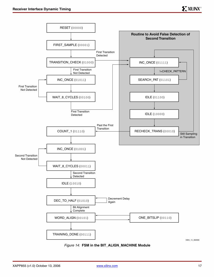
Receiver Interface Dynamic Timing
XAPP855 (v10) October 13 2006 wwwxilinxcom 17
R
Figure 14 FSM in the BIT_ALIGN_MACHINE Module
TRANSITION_CHECK (01000)
First TransitionNot Detected
First TransitionNot Detected
First TransitionDetected
First TransitionDetected
Past the FirstTransition
Second TransitionNot Detected
Second TransitionDetected
Decrement DelayAgain
Bit AlignmentComplete
Still Samplingin Transition
INC_ONCE (01111)
SEARCH_PAT (01101)
IDLE (01100)
IDLE (10000)
RECHECK_TRANS (00010)
ONE_BITSLIP (00110)
INC_ONCE (01011)
WAIT_8_CYCLES (00100)
COUNT_1 (01110)
INC_ONCE (01001)
WAIT_8_CYCLES (00011)
IDLE (10010)
TRAINING_DONE (00111)
FIRST_SAMPLE (00001)
RESET (00000)
DEC_TO_HALF (01010)
WORD_ALIGN (00101)
X855_14_082806
Routine to Avoid False Detection of Second Transition
=CHECK_PATTERN
Receiver Interface Dynamic Timing
XAPP855 (v10) October 13 2006 wwwxilinxcom 18
R
Interface Timing Budget
In addition to sampling the data as closely as possible to the center of the data eye the actual size of the data eye is important By accurately predicting the size of the data eye in the receiver the overall performance ceiling of the interface can be inferred The ideal data eye width is the period of the data rate (for example TBit_Period = 100 ns for 1000 Mbs) Both the transmitter and receiver circuits have sources of error that subtract from the ideal data eye The equation for the eye width at the output of the transmitter is shown in Equation 4 TJITTER is the peak-to-peak jitter of the clock source driving the transmitter data bus and forwarded clock TDCD is the maximum duty cycle distortion of the clock tree driving the data bus and forwarded clock Skew is not considered in the transmitter or receiver because the receiver calibrates out skew between channels by performing alignment on each channel individually
Equation 4
Equation 5 calculates the width of the data eye at the receiver flip-flops Ideally the eye width at the receiver is the same as the eye width at the output of the transmitter but there are sources of error in the transmission medium and receiver circuitry Duty cycle distortion must be considered again on the receiver clock tree TSAMP_BUFIO is the receiver sampling error due to drift caused by voltage and temperature variations TIDELAYPAT_JIT is the amount of pattern dependent jitter that is accumulated in each tap of the IDELAY chain For a clock pattern TIDELAYPAT_JIT is 0 pstap peak to peak For a data pattern with long and short run lengths of zeroes and ones (simulated by PRBS23) TIDELAYPAT_JIT is a finite value that must be considered in the timing budget
Equation 5
TBOARD_JITTER includes jitter induced by receiver input capacitance and the parasitics of the physical data path on the PCB TBOARD_JITTER must be determined by simulation as it varies as a function of frequency and for receivers of different types and vendors On the ML550 with a -2 speed-grade Virtex-5 device the TBOARD_JITTER is measured at roughly 200 ps at 900 Mbs (assuming data content equivalent to PRBS23) TQUANTIZATION_ERR or quantization error is caused by the granularity of the IDELAY tap chain Working with 75 ps increments it is not possible to utilize the entire data eye since inevitably some valid eye width is lost between two taps The value for this loss is 75 ps As long as the receiver eye width calculated using Equation 5 is greater than or equal to 0 the interface operates correctly over process voltage and temperature
For example Equation 6 and Equation 7 show the timing budget calculation for the DDR interface running at 900 Mbs in a -2 speed grade device on an ML550 evaluation board Refer to the data sheet for the most current values The TX interface is looped back to the RX interface on the same Virtex-5 FPGA as shown in Equation 2
Equation 6
Equation 7
Changes in voltage and temperature cause the data channels of the interface to drift relative to the clock If the DDR interface were to transfer user data for a long period of time over all specified conditions of temperature and voltage Equation 7 states that there would be at least 107 ps (one or two IDELAY taps) of data window remaining valid during all fluctuations of temperature and voltage Compare this calculation to the measurements in Table 12 page 21 Case 900 Mbs There are four taps that are error free under all conditions In ldquoAppendixrdquo there are three -2 devices tested at 900 Mbs and each has 4 4 and 3 taps respectively that are error free under all conditions
DATA_EYE_WIDTH_TX TBIT_PERIOD TJITTERndash TDCD_BUFIOndash=
DATA_EYE_WIDTH_RX DATA_EYE_WIDTH_TX
TBOARD_JITTER
ndash
TSAMP_BUFIOndash TDCD_BUFIOndash
TIDELAYPAT_JIT IDELAY taps in datapathtimes[ ]ndash
TQUANTIZATION_ERRndash
=
DATA_EYE_WIDTH_TX 1111 ps 25 psndash 100 psndash 986 ps= =
DATA_EYE_WIDTH_RX986 ps 200 psndash 400 psndash 100 psndash 8 ps 13 tapstimes[ ] 75 ps 107 ps=ndashndash
=
Interface Characterization
XAPP855 (v10) October 13 2006 wwwxilinxcom 19
R
At a given temperature and voltage setting the data valid window is much larger because there is no drift when temperature and voltage are constant The size of the data valid window under constant conditions is 107 ps + TSAMP_BUFIO which in this case is at least 507 ps (six or seven IDELAY taps) Compare this calculation to the measurements of any single condition in Table 12 Case 900 Mbs In the worst case (ndash5 supply) there are 7 taps that are error free
Equation 8 and Equation 9 show the same timing budget calculation for the DDR interface running at 10 Gbs in a -2 speed grade device on an ML550 Evaluation Board
Equation 8
Equation 9
Equation 9 predicts that no data window remains valid during all specified fluctuations of temperature and voltage (compare to Table 12 Case 1000 Mbs) In ldquoAppendixrdquo there are three -2 devices tested at 1000 Mbs and each has 1 3 and 1 taps respectively that are error free under all conditions This data rate and device combination are very marginal cases
To operate at 10 Gbs the DDR interface requires additional circuitry to track out voltage-temperature variations in real-time (see XAPP860 16-channel DDR LVDS Interface with Real-time Window Monitoring for a DDR Interface with real-time window monitoring) If the voltage-temperature variations are removed from the picture the predicted data valid window is ndash120 ps + TSAMP_BUFIO which in this case is at least 280 ps (3 or 4 taps) Compare this calculation to the measurements of any single condition in Table 18 page 34 There are at least four error-free taps in all conditions
Interface Characterization
By following the procedure illustrated in Figure 13 page 15 the bit-alignment algorithm should never insert more than approximately 15 bit times of delay on the data channels The fewest number of delay taps should be used in the datapath because they produce a finite amount of degradation (TIDELAYPAT_JIT) The worst-case initial timing for the algorithm occurs when the clock samples just before the data transitions as in the 600 Mbs case in Figure 12 page 14 The algorithm must move all the way through the first eye to find the first transition (1 bit time) and then move halfway into the next eye to center the sampling point (05 bit time) This process produces a worst-case total delay insertion of 15 bit times
The actual performance of the bit-alignment algorithm is characterized as a function of data rate in Figure 15 page 20 For all data rates the expectation is that the tap settings of all 16 channels in the DDR receiver do not exceed approximately 15 bit times of delay Both the maximum and minimum tap setting of all 16 channels is recorded for each data rate This graph only shows the data for a single device Comparing the 15 bit time mask to the actual settings it is clear that the algorithm remains within the 15 bit time limit At 13 Gbs the tap setting actually exceeds the mask by one tap (a negligible violation)
DATA_EYE_WIDTH_TX 1000 ps 25 psndash 100 psndash 875 ps= =
DATA_EYE_WIDTH_RX 875 ps 300 psndash400 ps 100 psndash
ndash8 ps 15 tapstimes[ ] 75 ps 120 psndash=ndashndash
=
Interface Characterization
XAPP855 (v10) October 13 2006 wwwxilinxcom 20
R
The maximum and minimum tap settings in Figure 15 generally stay within 3 to 4 taps of each other except in the case of 640 Mbs and 1300 Mbs data rates These data rates are seams in the inherent timing At data rates below 640 Mbs the tap settings are in the range of 30 taps and at data rates above 640 Mbs the tap settings are in the range of 12 taps Referring back to Figure 12 page 14 it is clear why this seam occurs As the data rate increases past 600 Mbs the initial sampling point of the inherent timing moves into a different data eye creating a different starting point for the algorithm At 640 Mbs some of the 16 channels start in one eye while other channels start in the other eye Fortunately this is not an issue because the single bit time of difference between the channels is resolved using bitslip
Referring back to Figure 8 page 9 the clock channel goes through an IDELAY block with a default value of 0 Once the data rate is chosen for a given design this initial IDELAY value can be changed to a non-zero value to achieve more favorable inherent timing For example a design running at 620 Mbs can use 30 IDELAY taps on the delay channels each contributing a certain amount of jitter to the timing budget calculation By setting the initial clock delay to 5 taps the inherent timing moves across the seam shown in the 600 Mbs range of Figure 15 causing the data channels to only use about 12 IDELAY taps Only spectrally rich data patterns accumulate jitter in the IDELAY tap chain so the clock IDELAY can be set to any value without diminishing the timing budget This optimization is entirely optional and can be done once the design is running in hardware
The DDR receiver is designed to remove skew between channels by aligning each channel individually The ML550 board on which this reference design is characterized is designed to have minimal skew between channels However there is clearly a finite amount of skew between channels due to clock skew in the TX and RX BUFIO networks package skew and trace length tolerance on the ML550 board Table 11 page 21 shows how the bit-alignment algorithm sets the delay for each channel differently to compensate for skew between channels The table captures the range of settings among the 16 channels at specific data rates for a -2 device If there were additional skew among the 16 channels then the tap setting range would be larger to compensate for it The algorithm is designed such that skew between channels should not diminish the performance of the interface The range of tap settings differs for different devices and speed grades but the magnitude should be approximately the same
Figure 15 Bit-Alignment Algorithm Performance
60
50
40
30
20
10
0200 400 600 800 1000 1200 1400 1600
Data Rate (Mbs)
Del
ay T
ap U
tiliz
atio
n HW Measurement (Min)HW Measurement (Max)15 Bit Time Mask
X855_15_072406
Interface Characterization
XAPP855 (v10) October 13 2006 wwwxilinxcom 21
R
Since the receiver alignment logic only runs once immediately after reset the resulting dynamic timing must be adequate to ensure error-free operation over the specified voltage and temperature variations that can occur over time The data-valid window at the receiver input must be wide enough to withstand these variations (receiver drift) Table 12 page 21 shows the data-valid window at the ISERDES registers in the DDR receiver The eyes shown are collective eyes of all 16 channels The BERT testbench configuration loops back the DDR transmitter to the DDR receiver Using pattern generators and error detectors programmed to send and receive a pseudorandom bit sequence (PRBS23) the width of the data-valid window is evaluated using pseudorandom data that closely resembles real user data
Table 11 Tap Setting Range For Various Data Rates Measured on a -2 Device
Data Rate (Mbs) Tap Setting Range Compensated Skew
500 31ndash34 4 taps
600 28ndash30 3 taps
700 10ndash12 3 taps
800 11ndash13 3 taps
900 11ndash13 3 taps
1000 13ndash15 3 taps
1100 13ndash15 3 taps
1200 14ndash15 2 taps
Table 12 Measurement of Receiver Drift under Extreme Conditions for Multiple Data Rates
ConditionIODELAY Taps (1)
ndash8 ndash7 ndash6 ndash5 ndash4 ndash3 ndash2 ndash1 0 +1 +2 +3 +4 +5 +6 +7 +8
Case 800 Mbs
25degC Nom Supplies F F F P P P P P C P P P P P F F F
0degC Nom Supplies F F F P P P P P P P P P P P F F F
85degC Nom Supplies F F F P P P P P P P P P P P F F F
25degC +5 Supplies F P P P P P P P P P P P F F F F F
0degC +5 Supplies F P P P P P P P P P P P F F F F F
85degC +5 Supplies F P P P P P P P P P P P F F F F F
25degC ndash5 Supplies F F F F F F P P P P P P P P P F F
0degC ndash5 Supplies F F F F F F P P P P P P P P P P F
85degC ndash5 Supplies F F F F F P P P P P P P P P P F F
CONCLUSION Error free under all conditions when calibrated under nominal conditions to position C
Interface Characterization
XAPP855 (v10) October 13 2006 wwwxilinxcom 22
R
Case 900 Mbs
25degC Nom Supplies F F F F P P P P C P P P P F F F F
0degC Nom Supplies F F F F P P P P P P P P P F F F F
85degC Nom Supplies F F F F P P P P P P P P F F F F F
25degC +5 Supplies F F P P P P P P P P P F F F F F F
0degC +5 Supplies F F P P P P P P P P P F F F F F F
85degC +5 Supplies F F P P P P P P P P P F F F F F F
25degC ndash5 Supplies F F F F F F F P P P P P P P P F F
0degC ndash5 Supplies F F F F F F F P P P P P P P P F F
85degC ndash5 Supplies F F F F F F F P P P P P P P F F F
CONCLUSION Error free under all conditions when calibrated under nominal conditions to position C
Case 1000 Mbs
25degC Nom Supplies F F F F F P P P C P P P F F F F F
0degC Nom Supplies F F F F F P P P P P P P F F F F F
85degC Nom Supplies F F F F F P P P P P P P F F F F F
25degC +5 Supplies F F F P P P P P P P F F F F F F F
0degC +5 Supplies F F F P P P P P P P F F F F F F F
85degC +5 Supplies F F F P P P P P P P P F F F F F F
25degC ndash5 Supplies F F F F F F F F P P P P P P F F F
0degC ndash5 Supplies F F F F F F F F P P P P P P F F F
85degC ndash5 Supplies F F F F F F F F P P P P P P F F F
CONCLUSION Error free under all conditions when calibrated under nominal conditions to position C
Case 1100 Mbs
25degC Nom Supplies F F F F F P P P C P F F F F F F F
0degC Nom Supplies F F F F F P P P P P F F F F F F F
85degC Nom Supplies F F F F F P P P P P F F F F F F F
25degC +5 Supplies F F F P P P P P P F F F F F F F F
0degC +5 Supplies F F F P P P P P P F F F F F F F F
85degC +5 Supplies F F F P P P P P P F F F F F F F F
25degC ndash5 Supplies F F F F F F F F P P P P F F F F F
0degC ndash5 Supplies F F F F F F F F P P P P F F F F F
85degC ndash5 Supplies F F F F F F F F P P P P F F F F F
CONCLUSION Error free under all conditions when calibrated under nominal conditions to position C
Table 12 Measurement of Receiver Drift under Extreme Conditions for Multiple Data Rates (Continued)
ConditionIODELAY Taps (1)
ndash8 ndash7 ndash6 ndash5 ndash4 ndash3 ndash2 ndash1 0 +1 +2 +3 +4 +5 +6 +7 +8
Interface Characterization
XAPP855 (v10) October 13 2006 wwwxilinxcom 23
R
In all test cases shown in Table 12 page 21 the bit-align machine accurately places the sampling point in the center of the data eye (indicated by the C in each test case) In the 1100 Mbs case the bit-align machine places the sampling point slightly off center This slight inaccuracy occurs when the center of a real data pattern diverges from the center of the training pattern The electrical behavior of different data patterns is discussed below
After the dynamic timing is established for a given test case under nominal conditions the device is subjected to extremes of temperature and voltage to stress the receiver timing At data rates of 1100 Mbs and below the dynamic timing established after reset under nominal conditions is sufficient to meet timing over all specified extreme conditions (the column with the C passes traffic error free under all conditions) At a data rate of 1200 Mbs the design operates correctly under nominal conditions but the data-valid window is not large enough to withstand the voltage variations For this particular transmission medium the 1200 Mbs case requires a real-time adjustment circuit that could track the center of the eye
The full datapath of the testbench consists of
TX rarr 5 FR-4 rarr SAMTEC QSE Conn rarr 12 Ribbon Cable rarr SAMTEC QSE Conn rarr 5 FR-4 rarr RX
For shorter transmission media higher performance can be achieved in accordance with the section ldquoInterface Timing Budgetrdquo page 18 Interface performance is not solely a question of the LVDS driver performance specification but rather a question of adequate timing margin to withstand production and environmental variations From Table 12 the total amount of variation experienced over temperature and voltage is roughly 375 ps (5 taps at 75 ps per tap) This number should be comparable to the specification for receiver sampling error (TSAMP_BUFIO) shown in the Virtex-5 Data Sheet
Case 1200 Mbs
25degC Nom Supplies F F F F F F P P C P F F F F F F F
0degC Nom Supplies F F F F F F P P P P F F F F F F F
85degC Nom Supplies F F F F F F P P P F F F F F F F F
25degC +5 Supplies F F F F P P P P F F F F F F F F F
0degC +5 Supplies F F F P P P P P F F F F F F F F F
85degC +5 Supplies F F F F P P P P F F F F F F F F F
25degC ndash5 Supplies F F F F F F F F F P P P F F F F F
0degC ndash5 Supplies F F F F F F F F F P P P F F F F F
85degC ndash5 Supplies F F F F F F F F F P P F F F F F F
CONCLUSION Errors caused by plusmn5 variations in supply voltages
Notes 1 Where 0 is the reference tap determined by the bit-align machine under nominal conditions at 25degC2 P = Error-free transmission F = Error in transmission C = IODELAY tap position selected by bit-align machine under nominal conditions at 25degC3 Device under test is -2 speed grade
Table 12 Measurement of Receiver Drift under Extreme Conditions for Multiple Data Rates (Continued)
ConditionIODELAY Taps (1)
ndash8 ndash7 ndash6 ndash5 ndash4 ndash3 ndash2 ndash1 0 +1 +2 +3 +4 +5 +6 +7 +8
Interface Characterization
XAPP855 (v10) October 13 2006 wwwxilinxcom 24
R
Pattern Dependence of Receiver Performance
Different types of data patterns have different electrical signatures (rise and fall times jitter eye symmetry etc) A pattern with very narrow spectral content (such as a clock pattern) moves very favorably through the link because the receiver frequency response has little effect on the signal integrity However a pattern with wide spectral content (such as real data and pseudorandom patterns) stresses the links frequency response If the frequency response is not flat across the entire spectrum of the data content then the signal integrity is degraded as a result The amount of degradation measured is shown in Table 13 page 25 The DDR transmitter is looped back to the DDR receiver and different patterns are programmed to traverse the link Performance is assessed by evaluating the integrity of those patterns in the receiver
PRBS7 is a pseudorandom data pattern with a maximum run length of seven consecutive zeroes or ones PRBS15 is defined as having a maximum run length of fifteen consecutive zeroes or ones These limitations on run lengths limit the spectral content of the pattern A PRBS15 pattern has greater spectral content than a PRBS7 pattern and therefore is a more strenuous test for the link PRBS29 is the most strenuous test in Table 13 A clock pattern is effectively a PRBS1
As predicted Table 13 shows that there is more degradation for data patterns with more spectral content At 1000 Mbs and below the data eye closure is symmetrical Symmetrical eye closure is desired because it does not change the center of the eye as determined by the bit-alignment algorithm Above 1000 Mbs the eye closure becomes more asymmetrical causing the center of the data eye to diverge from the calibrated center (by only 1 tap)
In every data rate shown in Table 13 all significant pattern-dependent degradation is caused between PRBS1 (clock pat) and PRBS15 Between PRBS15 and PRBS29 there is no additional degradation recorded in any of the measurements
Interface Characterization
XAPP855 (v10) October 13 2006 wwwxilinxcom 25
R
Table 13 Link Performance for Various Types of Data Measured on a -2 Device
PatternIODELAY Taps (1)
ndash8 ndash7 ndash6 ndash5 ndash4 ndash3 ndash2 ndash1 0 +1 +2 +3 +4 +5 +6 +7 +8 +9
Case 600 Mbs
Clock Pat (0101) P P P P P P P P C P P P P P P P P P
Training Pat (0x2C) P P P P P P P P C P P P P P P P P F
PRBS7 P P P P P P P P C P P P P P P P P F
PRBS15 F P P P P P P P C P P P P P P P F F
PRBS23 F P P P P P P P C P P P P P P P F F
PRBS29 F P P P P P P P C P P P P P P P F F
Case 800 Mbs
Clock Pat (0101) F F P P P P P P C P P P P P P F F F
Training Pat (0x2C) F F P P P P P P C P P P P P P F F F
PRBS7 F F P P P P P P C P P P P P F F F F
PRBS15 F F F P P P P P C P P P P P F F F F
PRBS23 F F F P P P P P C P P P P P F F F F
PRBS29 F F F P P P P P C P P P P P F F F F
Case 1000 Mbs
Clock Pat (0101) F F F P P P P P C P P P P P F F F F
Training Pat (0x2C) F F F P P P P P C P P P P F F F F F
PRBS7 F F F F P P P P C P P P F F F F F F
PRBS15 F F F F F P P P C P P P F F F F F F
PRBS23 F F F F F P P P C P P P F F F F F F
PRBS29 F F F F F P P P C P P P F F F F F F
Case 1200 Mbs
Clock Pat (0101) F F F F P P P P C P P P P F F F F F
Training Pat (0x2C) F F F F P P P P C P P P F F F F F F
PRBS7 F F F F F P P P C P F F F F F F F F
PRBS15 F F F F F F P P C F F F F F F F F F
PRBS23 F F F F F F P P C F F F F F F F F F
PRBS29 F F F F F F P P C F F F F F F F F F
Case 1400 Mbs
Clock Pat (0101) F F F F F F P P C P P P F F F F F F
Training Pat (0x2C) F F F F F P P P C P P F F F F F F F
PRBS7 F F F F F F F P C P F F F F F F F F
PRBS15 F F F F F F F P C F F F F F F F F F
PRBS23 F F F F F F F P C F F F F F F F F F
PRBS29 F F F F F F F P C F F F F F F F F F
Notes 1 Where 0 is the reference tap determined by the bit-align machine under nominal conditions at 25degC2 P = Error-free transmission F = Error in transmission C = IODELAY tap position selected by bit-align machine under nominal conditions at 25degC
Resetting the Interface
XAPP855 (v10) October 13 2006 wwwxilinxcom 26
R
Resetting the Interface
Several dependencies determine the order in which circuits should be reset in the interface The receiver cannot begin the alignment algorithm if the transmitter is not sending the training pattern The transmitter must be reset before the receiver and time must be allowed for the training pattern to propagate across the link before the receiver comes out of reset The receiver also cannot begin the alignment algorithm until IDELAYCTRL has recovered from reset which could takes hundreds of cycles The recommended reset timing for the interface is shown in Figure 16 This reset timing is implemented in the BERT testbench for this interface
The TX reset (RST_TX) is used to reset all TX circuitry and also IDELAYCTRL The IDELAYCTRL reset is asynchronous so driving it with RST_TX is acceptable The minimum pulse width of IDELAYCTRL reset is 50 ns (TIDELAYCTRL_RPW) For that reason resets are held High for 16 clock cycles The RX reset (RST_RX) is used to reset all RX circuitry and is asserted when the IDELAYCTRL READY flag goes High indicating that the IODELAY blocks are calibrated
The timing of the READY flag in Figure 16 is a potential hazard Most likely it is High during a TX reset because it takes many cycles for IDELAYCTRL to deassert the READY flag It is easy to make the mistake of resetting the receiver too early To avoid this hazard the RX reset should be asserted only after seeing a deassertion and reassertion of the READY flag
Conclusion Based on the design and characterization described in this document the 16-Channel DDR reference design operates to the performance targets in Table 14 under all conditions of process voltage and temperature However to meet these targets over voltage and temperature the timing budget must be guaranteed according to the analysis in ldquoInterface Timing Budgetrdquo See ldquoAppendixrdquo page 27 for further justification of the maximum performance recommendations in Table 14
Figure 16 Recommended Interface Reset Timing
RST_TX
IDELAYCTRLREADY
RST_RX
16 Cycles X855_16_072406
Table 14 Performance of 16-Channel DDR Interface
Speed Grade Maximum Performance
-1 800 Mbs
-2 900 Mbs
-3 10 Gbs(1)
Notes 1 To achieve higher performance (up to 125 Gbs) see 16-channel DDR LVDS Interface with Realtime
Window Monitoring for an example of a DDR interface with real-time window monitoring
Appendix
XAPP855 (v10) October 13 2006 wwwxilinxcom 27
R
Appendix Performance Characterization Data
Refer to ldquoInterface Characterizationrdquo page 19 for explanations about how to interpret the data in the ldquoAppendixrdquo These tables show collective data eyes for the entire interface over process voltage and temperature (PVT) Three devices from each speed grade were selected for this characterization
The calibrated center position of the eye (marked by the C in the tables below) varies slightly from channel to channel (due to small skews between channels) That range is referred to as center tap range Analysis of Table 16 page 28 through Table 20 page 40 shows that the center tap range for slow and fast parts differ significantly at the same data rate (because the BIT_ALIGN_MACHINE algorithm adjusts for differences in speed)
All data in the ldquoAppendixrdquo is collected using the BERT testbench shown in Figure 2 page 2 The data pattern is PRBS23 and the devicepackage is XC5VLX50T-FF1136 The transmission path for the cases shown in Table 16 through Table 20 is repeated for convenience
TX rarr 5 FR-4 rarr SAMTEC QSE Conn rarr 12 Ribbon Cable rarr SAMTEC QSE Conn rarr 5 FR-4 rarr RX
A summary of these characterization results is shown in Table 15 Each of the nine parts were tested at 800 900 1000 1100 and 1200 Mbs When the interface is error free on all channels under all extreme conditions of temperature and voltage the particular test case is designated by a P A test case is marked FAIL when the interface suffered errors on any channel under any particular condition of voltage and temperature
Table 15 Summary of Interface Characterization Results
Device (SN) Speed Grade 800 Mbs 900 Mbs 1000Mbs 1100 Mbs 1200 Mbs
2194 -1 P P P FAIL FAIL
2219 -1 P FAIL FAIL FAIL FAIL
2199 -1 P P FAIL FAIL FAIL
001 -2 P P FAIL P FAIL
002 -2 P P P P FAIL
003 -2 P P FAIL FAIL FAIL
004 -3 P P P P P
005 -3 P P P P P
006 -3 P P P P P
Appendix
XAPP855 (v10) October 13 2006 wwwxilinxcom 28
R
Table 16 Measurement of Receiver Drift under Extreme Conditions at 800 Mbs
ConditionIODELAY Taps (1)
ndash8 ndash7 ndash6 ndash5 ndash4 ndash3 ndash2 ndash1 0 +1 +2 +3 +4 +5 +6 +7 +8
SN 2194 Speed Grade -1
25degC Nom Supplies F F F P P P P P C P P P P F F F F
0degC Nom Supplies F F F P P P P P P P P P P F F F F
85degC Nom Supplies F F F F P P P P P P P P P F F F F
25degC +5 Supplies F F P P P P P P P P P P F F F F F
0degC +5 Supplies F F P P P P P P P P P P F F F F F
85degC +5 Supplies F F P P P P P P P P P P F F F F F
25degC ndash5 Supplies F F F F F F P P P P P P P P P F F
0degC ndash5 Supplies F F F F F F P P P P P P P P P F F
85degC ndash5 Supplies F F F F F F P P P P P P P P P F F
Center Tap Range Taps 11ndash12
CONCLUSION Error free under all conditions when calibrated under nominal conditions to position C
SN 2219 Speed Grade -1
25degC Nom Supplies F F F P P P P P C P P P F F F F F
0degC Nom Supplies F F F P P P P P P P P P F F F F F
85degC Nom Supplies F F F P P P P P P P P P F F F F F
25degC +5 Supplies F P P P P P P P P P P F F F F F F
0degC +5 Supplies F P P P P P P P P P P F F F F F F
85degC +5 Supplies F P P P P P P P P P P F F F F F F
25degC ndash5 Supplies F F F F F F P P P P P P P P F F F
0degC ndash5 Supplies F F F F F F F P P P P P P P F F F
85degC ndash5 Supplies F F F F F F P P P P P P P P F F F
Center Tap Range Taps 13ndash16
CONCLUSION Error free under all conditions when calibrated under nominal conditions to position C
SN 2199 Speed Grade -1
25degC Nom Supplies F F F P P P P P C P P P P F F F F
0degC Nom Supplies F F F P P P P P P P P P P F F F F
85degC Nom Supplies F F F P P P P P P P P P P F F F F
25degC +5 Supplies F P P P P P P P P P P P F F F F F
0degC +5 Supplies F P P P P P P P P P P P F F F F F
85degC +5 Supplies F P P P P P P P P P P P F F F F F
25degC ndash5 Supplies F F F F F F P P P P P P P P P F F
0degC ndash5 Supplies F F F F F F P P P P P P P P P F F
85degC ndash5 Supplies F F F F F F P P P P P P P P P F F
Center Tap Range Taps 10ndash12
CONCLUSION Error free under all conditions when calibrated under nominal conditions to position C
Appendix
XAPP855 (v10) October 13 2006 wwwxilinxcom 29
R
SN 001 Speed Grade -2
25degC Nom Supplies F F F P P P P P C P P P P F F F F
0degC Nom Supplies F F F P P P P P P P P P P F F F F
85degC Nom Supplies F F F P P P P P P P P P P F F F F
25degC +5 Supplies F P P P P P P P P P P P F F F F F
0degC +5 Supplies F P P P P P P P P P P F F F F F F
85degC +5 Supplies F P P P P P P P P P P P F F F F F
25degC ndash5 Supplies F F F F F P P P P P P P P P P F F
0degC ndash5 Supplies F F F F F P P P P P P P P P P F F
85degC ndash5 Supplies F F F F F P P P P P P P P P P F F
Center Tap Range Taps 10ndash12
CONCLUSION Error free under all conditions when calibrated under nominal conditions to position C
SN 002 Speed Grade -2
25degC Nom Supplies F F F P P P P P C P P P P F F F F
0degC Nom Supplies F F F P P P P P P P P P P F F F F
85degC Nom Supplies F F F P P P P P P P P P P F F F F
25degC +5 Supplies F P P P P P P P P P P P F F F F F
0degC +5 Supplies F P P P P P P P P P P P F F F F F
85degC +5 Supplies F F P P P P P P P P P P F F F F F
25degC ndash5 Supplies F F F F F P P P P P P P P P P F F
0degC ndash5 Supplies F F F F F P P P P P P P P P P F F
85degC ndash5 Supplies F F F F F P P P P P P P P P P F F
Center Tap Range Taps 10ndash12
CONCLUSION Error free under all conditions when calibrated under nominal conditions to position C
SN 003 Speed Grade -2
25degC Nom Supplies F F F P P P P P C P P P P F F F F
0degC Nom Supplies F F F P P P P P P P P P P F F F F
85degC Nom Supplies F F F P P P P P P P P P P F F F F
25degC +5 Supplies F P P P P P P P P P P P F F F F F
0degC +5 Supplies F P P P P P P P P P P F F F F F F
85degC +5 Supplies F P P P P P P P P P P P F F F F F
25degC ndash5 Supplies F F F F F F P P P P P P P P P F F
0degC ndash5 Supplies F F F F F F P P P P P P P P P F F
85degC ndash5 Supplies F F F F F F P P P P P P P P P F F
Center Tap Range Taps 11ndash13
CONCLUSION Error free under all conditions when calibrated under nominal conditions to position C
Table 16 Measurement of Receiver Drift under Extreme Conditions at 800 Mbs (Continued)
ConditionIODELAY Taps (1)
ndash8 ndash7 ndash6 ndash5 ndash4 ndash3 ndash2 ndash1 0 +1 +2 +3 +4 +5 +6 +7 +8
Appendix
XAPP855 (v10) October 13 2006 wwwxilinxcom 30
R
SN 004 Speed Grade -3
25degC Nom Supplies F F F P P P P P C P P P P F F F F
0degC Nom Supplies F F F P P P P P P P P P F F F F F
85degC Nom Supplies F F F P P P P P P P P P P F F F F
25degC +5 Supplies F P P P P P P P P P P P F F F F F
0degC +5 Supplies F P P P P P P P P P P P F F F F F
85degC +5 Supplies F F P P P P P P P P P P F F F F F
25degC ndash5 Supplies F F F F F P P P P P P P P P F F F
0degC ndash5 Supplies F F F F F P P P P P P P P P F F F
85degC ndash5 Supplies F F F F F P P P P P P P P P F F F
Center Tap Range Taps 8ndash9 23ndash24
CONCLUSION Error free under all conditions when calibrated under nominal conditions to position C
SN 005 Speed Grade -3
25degC Nom Supplies F F P P P P P P C P P P P F F F F
0degC Nom Supplies F F P P P P P P P P P P P F F F F
85degC Nom Supplies F F F P P P P P P P P P P P F F F
25degC +5 Supplies F P P P P P P P P P P P F F F F F
0degC +5 Supplies F P P P P P P P P P P P F F F F F
85degC +5 Supplies F P P P P P P P P P P P F F F F F
25degC ndash5 Supplies F F F F P P P P P P P P P P P F F
0degC ndash5 Supplies F F F F P P P P P P P P P P P F F
85degC ndash5 Supplies F F F F P P P P P P P P P P P F F
Center Tap Range Taps 9ndash10
CONCLUSION Error free under all conditions when calibrated under nominal conditions to position C
SN 006 Speed Grade -3
25degC Nom Supplies F F P P P P P P C P P P P F F F F
0degC Nom Supplies F F P P P P P P P P P P P F F F F
85degC Nom Supplies F F F P P P P P P P P P P F F F F
25degC +5 Supplies F P P P P P P P P P P P F F F F F
0degC +5 Supplies F P P P P P P P P P P P F F F F F
85degC +5 Supplies F F P P P P P P P P P P F F F F F
25degC ndash5 Supplies F F F P P P P P P P P P P P F F F
0degC ndash5 Supplies F F F P P P P P P P P P P P F F F
85degC ndash5 Supplies F F F F F P P P P P P P P P F F F
Center Tap Range Taps 8ndash9 23ndash24
CONCLUSION Error free under all conditions when calibrated under nominal conditions to position C
Notes 1 IODELAY taps where 0 is the reference tap determined by the bit align machine at nominal voltage and 25degC2 P = Error-free transmission F = Error in transmission C = IODELAY tap position selected by bit-align machine under nominal conditions at 25degC
Table 16 Measurement of Receiver Drift under Extreme Conditions at 800 Mbs (Continued)
ConditionIODELAY Taps (1)
ndash8 ndash7 ndash6 ndash5 ndash4 ndash3 ndash2 ndash1 0 +1 +2 +3 +4 +5 +6 +7 +8
Appendix
XAPP855 (v10) October 13 2006 wwwxilinxcom 31
R
Table 17 Measurement of Receiver Drift under Extreme Conditions at 900 Mbs
ConditionIODELAY Taps (1)
ndash8 ndash7 ndash6 ndash5 ndash4 ndash3 ndash2 ndash1 0 +1 +2 +3 +4 +5 +6 +7 +8
SN 2194 Speed Grade -1
25degC Nom Supplies F F F F F P P P C P P P F F F F F
0degC Nom Supplies F F F F F P P P P P P P F F F F F
85degC Nom Supplies F F F F F P P P P P P P P F F F F
25degC +5 Supplies F F F P P P P P P P P F F F F F F
0degC +5 Supplies F F F P P P P P P P P F F F F F F
85degC +5 Supplies F F F P P P P P P P P F F F F F F
25degC ndash5 Supplies F F F F F F F P P P P P P P F F F
0degC ndash5 Supplies F F F F F F F P P P P P P P F F F
85degC ndash5 Supplies F F F F F F F P P P P P P P F F F
Center Tap Range Taps 11ndash12
CONCLUSION Error free under all conditions when calibrated under nominal conditions to position C
SN 2219 Speed Grade -1
25degC Nom Supplies F F F F F P P P C P P P F F F F F
0degC Nom Supplies F F F F F P P P P P P P F F F F F
85degC Nom Supplies F F F F F P P P P P P P F F F F F
25degC +5 Supplies F F F P P P P P P P F F F F F F F
0degC +5 Supplies F F F P P P P P P P F F F F F F F
85degC +5 Supplies F F F P P P P P P P F F F F F F F
25degC ndash5 Supplies F F F F F F F F F P P P P P F F F
0degC ndash5 Supplies F F F F F F F F F P P P P P F F F
85degC ndash5 Supplies F F F F F F F F P P P P P P F F F
Center Tap Range Taps 12ndash15
CONCLUSION Errors caused by ndash5 variation in supply voltage
SN 2199 Speed Grade -1
25degC Nom Supplies F F F F F P P P C P P P F F F F F
0degC Nom Supplies F F F F F P P P P P P P F F F F F
85degC Nom Supplies F F F F F P P P P P P P F F F F F
25degC +5 Supplies F F F P P P P P P P P F F F F F F
0degC +5 Supplies F F F P P P P P P P P F F F F F F
85degC +5 Supplies F F F P P P P P P P P F F F F F F
25degC ndash5 Supplies F F F F F F F F P P P P P P F F F
0degC ndash5 Supplies F F F F F F F F P P P P P P F F F
85degC ndash5 Supplies F F F F F F F F P P P P P P F F F
Center Tap Range Taps 10ndash12
CONCLUSION Error free under all conditions when calibrated under nominal conditions to position C
Appendix
XAPP855 (v10) October 13 2006 wwwxilinxcom 32
R
SN 001 Speed Grade -2
25degC Nom Supplies F F F F P P P P C P P P P F F F F
0degC Nom Supplies F F F F P P P P P P P P P F F F F
85degC Nom Supplies F F F F F P P P P P P P P F F F F
25degC +5 Supplies F F P P P P P P P P P F F F F F F
0degC +5 Supplies F F P P P P P P P P P F F F F F F
85degC +5 Supplies F F F P P P P P P P P P F F F F F
25degC ndash5 Supplies F F F F F F F P P P P P P P F F F
0degC ndash5 Supplies F F F F F F F P P P P P P P F F F
85degC ndash5 Supplies F F F F F F F P P P P P P P F F F
Center Tap Range Taps 9ndash11
CONCLUSION Error free under all conditions when calibrated under nominal conditions to position C
SN 002 Speed Grade -2
25degC Nom Supplies F F F F P P P P C P P P P F F F F
0degC Nom Supplies F F F F P P P P P P P P F F F F F
85degC Nom Supplies F F F F F P P P P P P P P F F F F
25degC +5 Supplies F F F P P P P P P P P F F F F F F
0degC +5 Supplies F F F P P P P P P P P F F F F F F
85degC +5 Supplies F F F P P P P P P P P P F F F F F
25degC ndash5 Supplies F F F F F F F P P P P P P P F F F
0degC ndash5 Supplies F F F F F F F P P P P P P P F F F
85degC ndash5 Supplies F F F F F F F P P P P P P P F F F
Center Tap Range Taps 10ndash12
CONCLUSION Error free under all conditions when calibrated under nominal conditions to position C
SN 003 Speed Grade -2
25degC Nom Supplies F F F F F P P P C P P P P F F F F
0degC Nom Supplies F F F F F P P P P P P P P F F F F
85degC Nom Supplies F F F F F P P P P P P P P F F F F
25degC +5 Supplies F F P P P P P P P P P F F F F F F
0degC +5 Supplies F F P P P P P P P P P F F F F F F
85degC +5 Supplies F F F P P P P P P P P F F F F F F
25degC ndash5 Supplies F F F F F F F P P P P P P P F F F
0degC ndash5 Supplies F F F F F F F F P P P P P P F F F
85degC ndash5 Supplies F F F F F F F P P P P P P P F F F
Center Tap Range Taps 11ndash13
CONCLUSION Error free under all conditions when calibrated under nominal conditions to position C
Table 17 Measurement of Receiver Drift under Extreme Conditions at 900 Mbs (Continued)
ConditionIODELAY Taps (1)
ndash8 ndash7 ndash6 ndash5 ndash4 ndash3 ndash2 ndash1 0 +1 +2 +3 +4 +5 +6 +7 +8
Appendix
XAPP855 (v10) October 13 2006 wwwxilinxcom 33
R
SN 004 Speed Grade -3
25degC Nom Supplies F F F F P P P P C P P P P F F F F
0degC Nom Supplies F F F P P P P P P P P P P F F F F
85degC Nom Supplies F F F F P P P P P P P P P F F F F
25degC +5 Supplies F F F P P P P P P P P P F F F F F
0degC +5 Supplies F F F P P P P P P P P P F F F F F
85degC +5 Supplies F F F P P P P P P P P P F F F F F
25degC ndash5 Supplies F F F F F F P P P P P P P P F F F
0degC ndash5 Supplies F F F F F F P P P P P P P P F F F
85degC ndash5 Supplies F F F F F F P P P P P P P P F F F
Center Tap Range Taps 7ndash8
CONCLUSION Error free under all conditions when calibrated under nominal conditions to position C
SN 005 Speed Grade ndash3
25degC Nom Supplies F F F P P P P P C P P P P F F F F
0degC Nom Supplies F F F P P P P P P P P P P F F F F
85degC Nom Supplies F F F F P P P P P P P P P F F F F
25degC +5 Supplies F F P P P P P P P P P P F F F F F
0degC +5 Supplies F F P P P P P P P P P P F F F F F
85degC +5 Supplies F F F P P P P P P P P P F F F F F
25degC ndash5 Supplies F F F F F F P P P P P P P P F F F
0degC ndash5 Supplies F F F F F P P P P P P P P P F F F
85degC ndash5 Supplies F F F F F F P P P P P P P P F F F
Center Tap Range Taps 9ndash10
CONCLUSION Error free under all conditions when calibrated under nominal conditions to position C
SN 006 Speed Grade -3
25degC Nom Supplies F F F F P P P P C P P P P F F F F
0degC Nom Supplies F F F F P P P P P P P P P F F F F
85degC Nom Supplies F F F F P P P P P P P P P F F F F
25degC +5 Supplies F F P P P P P P P P P P F F F F F
0degC +5 Supplies F F P P P P P P P P P P F F F F F
85degC +5 Supplies F F F P P P P P P P P P F F F F F
25degC ndash5 Supplies F F F F F P P P P P P P P P F F F
0degC ndash5 Supplies F F F F F P P P P P P P P P F F F
85degC ndash5 Supplies F F F F F F P P P P P P P P F F F
Center Tap Range Taps 7ndash8
CONCLUSION Error free under all conditions when calibrated under nominal conditions to position C
Notes 1 IODELAY taps where 0 is the reference tap determined by the bit align machine at nominal voltage and 25degC2 P = Error-free transmission F = Error in transmission C = IODELAY tap position selected by bit-align machine under nominal conditions at 25degC
Table 17 Measurement of Receiver Drift under Extreme Conditions at 900 Mbs (Continued)
ConditionIODELAY Taps (1)
ndash8 ndash7 ndash6 ndash5 ndash4 ndash3 ndash2 ndash1 0 +1 +2 +3 +4 +5 +6 +7 +8
Appendix
XAPP855 (v10) October 13 2006 wwwxilinxcom 34
R
Table 18 Measurement of Receiver Drift under Extreme Conditions at 1000 Mbs
ConditionIODELAY Taps (1)
ndash8 ndash7 ndash6 ndash5 ndash4 ndash3 ndash2 ndash1 0 +1 +2 +3 +4 +5 +6 +7 +8
SN 2194 Speed Grade -1
25degC Nom Supplies F F F F F P P P C P P F F F F F F
0degC Nom Supplies F F F F F P P P P P P F F F F F F
85degC Nom Supplies F F F F F P P P P P P F F F F F F
25degC +5 Supplies F F F P P P P P P P F F F F F F F
0degC +5 Supplies F F F P P P P P P P F F F F F F F
85degC +5 Supplies F F F F P P P P P P F F F F F F F
25degC ndash5 Supplies F F F F F F F F P P P P P F F F F
0degC ndash5 Supplies F F F F F F F F P P P P P F F F F
85degC ndash5 Supplies F F F F F F F F P P P P P F F F F
Center Tap Range Taps 12ndash13
CONCLUSION Error free under all conditions when calibrated under nominal conditions to position C
SN 2219 Speed Grade -1
25degC Nom Supplies F F F F F F P P C P P F F F F F F
0degC Nom Supplies F F F F F F P P P P P F F F F F F
85degC Nom Supplies F F F F F F P P P P P F F F F F F
25degC +5 Supplies F F F P P P P P P F F F F F F F F
0degC +5 Supplies F F F P P P P P P F F F F F F F F
85degC +5 Supplies F F F F P P P P P F F F F F F F F
25degC ndash5 Supplies F F F F F F F F F P P P P F F F F
0degC ndash5 Supplies F F F F F F F F F F P P P F F F F
85degC ndash5 Supplies F F F F F F F F F P P P P F F F F
Center Tap Range Taps 14ndash17
CONCLUSION Errors caused by ndash5 variation in supply voltage
SN 2199 Speed Grade -1
25degC Nom Supplies F F F F F F P P C P P F F F F F F
0degC Nom Supplies F F F F F F P P P P P F F F F F F
85degC Nom Supplies F F F F F F P P P P P F F F F F F
25degC +5 Supplies F F F F P P P P P P F F F F F F F
0degC +5 Supplies F F F F P P P P P P F F F F F F F
85degC +5 Supplies F F F F P P P P P P F F F F F F F
25degC ndash5 Supplies F F F F F F F F F P P P P F F F F
0degC ndash5 Supplies F F F F F F F F F P P P P F F F F
85degC ndash5 Supplies F F F F F F F F F P P P P F F F F
Center Tap Range Taps 12ndash14
CONCLUSION Errors caused by ndash5 variation in supply voltage
Appendix
XAPP855 (v10) October 13 2006 wwwxilinxcom 35
R
SN 001 Speed Grade -2
25degC Nom Supplies F F F F F F P P C P P P F F F F F
0degC Nom Supplies F F F F F F P P P P P P F F F F F
85degC Nom Supplies F F F F F F P P P P P P F F F F F
25degC +5 Supplies F F F F P P P P P P F F F F F F F
0degC +5 Supplies F F F F P P P P P P F F F F F F F
85degC +5 Supplies F F F F P P P P P P P F F F F F F
25degC ndash5 Supplies F F F F F F F F F P P P P F F F F
0degC ndash5 Supplies F F F F F F F F F P P P P F F F F
85degC ndash5 Supplies F F F F F F F F F P P P P F F F F
Center Tap Range Taps 11ndash12
CONCLUSION Errors caused by ndash5 variation in supply voltage
SN 002 Speed Grade -2
25degC Nom Supplies F F F F F P P P C P P F F F F F F
0degC Nom Supplies F F F F F P P P P P P P F F F F F
85degC Nom Supplies F F F F F P P P P P P P F F F F F
25degC +5 Supplies F F F F P P P P P P F F F F F F F
0degC +5 Supplies F F F P P P P P P P F F F F F F F
85degC +5 Supplies F F F F P P P P P P P F F F F F F
25degC ndash5 Supplies F F F F F F F P P P P P P F F F F
0degC ndash5 Supplies F F F F F F F P P P P P P F F F F
85degC ndash5 Supplies F F F F F F F P P P P P P F F F F
Center Tap Range Taps 11ndash13
CONCLUSION Error free under all conditions when calibrated under nominal conditions to position C
SN 003 Speed Grade -2
25degC Nom Supplies F F F F F F P P C P P F F F F F F
0degC Nom Supplies F F F F F F P P P P P F F F F F F
85degC Nom Supplies F F F F F F P P P P P F F F F F F
25degC +5 Supplies F F F F P P P P P P F F F F F F F
0degC +5 Supplies F F F F P P P P P P F F F F F F F
85degC +5 Supplies F F F F P P P P P P F F F F F F F
25degC ndash5 Supplies F F F F F F F F F P P P P F F F F
0degC ndash5 Supplies F F F F F F F F F P P P P F F F F
85degC ndash5 Supplies F F F F F F F F F P P P P F F F F
Center Tap Range Taps 13ndash14
CONCLUSION Errors caused by ndash5 variation in supply voltage
Table 18 Measurement of Receiver Drift under Extreme Conditions at 1000 Mbs (Continued)
ConditionIODELAY Taps (1)
ndash8 ndash7 ndash6 ndash5 ndash4 ndash3 ndash2 ndash1 0 +1 +2 +3 +4 +5 +6 +7 +8
Appendix
XAPP855 (v10) October 13 2006 wwwxilinxcom 36
R
SN 004 Speed Grade -3
25degC Nom Supplies F F F F F P P P C P P P F F F F F
0degC Nom Supplies F F F F F P P P P P P P F F F F F
85degC Nom Supplies F F F F F P P P P P P P F F F F F
25degC +5 Supplies F F F P P P P P P P P F F F F F F
0degC +5 Supplies F F F P P P P P P P P F F F F F F
85degC +5 Supplies F F F F P P P P P P P P F F F F F
25degC ndash5 Supplies F F F F F F F P P P P P P F F F F
0degC ndash5 Supplies F F F F F F F P P P P P P F F F F
85degC ndash5 Supplies F F F F F F F P P P P P P P F F F
Center Tap Range Taps 9ndash10
CONCLUSION Error free under all conditions when calibrated under nominal conditions to position C
SN 005 Speed Grade -3
25degC Nom Supplies F F F F P P P P C P P P F F F F F
0degC Nom Supplies F F F F P P P P P P P P F F F F F
85degC Nom Supplies F F F F P P P P P P P P F F F F F
25degC +5 Supplies F F F P P P P P P P P F F F F F F
0degC +5 Supplies F F P P P P P P P P P F F F F F F
85degC +5 Supplies F F F P P P P P P P P F F F F F F
25degC ndash5 Supplies F F F F F F P P P P P P P P F F F
0degC ndash5 Supplies F F F F F F P P P P P P P P F F F
85degC ndash5 Supplies F F F F F F P P P P P P P F F F F
Center Tap Range Taps 11ndash12
CONCLUSION Error free under all conditions when calibrated under nominal conditions to position C
SN 006 Speed Grade -3
25degC Nom Supplies F F F F P P P P C P P P F F F F F
0degC Nom Supplies F F F F P P P P P P P P F F F F F
85degC Nom Supplies F F F F P P P P P P P P F F F F F
25degC +5 Supplies F F F P P P P P P P P F F F F F F
0degC +5 Supplies F F F P P P P P P P P F F F F F F
85degC +5 Supplies F F F P P P P P P P P F F F F F F
25degC ndash5 Supplies F F F F F F P P P P P P P F F F F
0degC ndash5 Supplies F F F F F F P P P P P P P F F F F
85degC ndash5 Supplies F F F F F F P P P P P P P F F F F
Center Tap Range Taps 9ndash10
CONCLUSION Error free under all conditions when calibrated under nominal conditions to position C
Notes 1 IODELAY taps where 0 is the reference tap determined by the bit align machine at nominal voltage and 25degC2 P = Error-free transmission F = Error in transmission C = IODELAY tap position selected by bit-align machine under nominal conditions at 25degC
Table 18 Measurement of Receiver Drift under Extreme Conditions at 1000 Mbs (Continued)
ConditionIODELAY Taps (1)
ndash8 ndash7 ndash6 ndash5 ndash4 ndash3 ndash2 ndash1 0 +1 +2 +3 +4 +5 +6 +7 +8
Appendix
XAPP855 (v10) October 13 2006 wwwxilinxcom 37
R
Table 19 Measurement of Receiver Drift under Extreme Conditions at 1100 Mbs
ConditionIODELAY Taps (1)
ndash8 ndash7 ndash6 ndash5 ndash4 ndash3 ndash2 ndash1 0 +1 +2 +3 +4 +5 +6 +7 +8
SN 2194 Speed Grade -1
25degC Nom Supplies F F F F F F P P C P P F F F F F F
0degC Nom Supplies F F F F F F P P P P P F F F F F F
85degC Nom Supplies F F F F F F P P P P P F F F F F F
25degC +5 Supplies F F F F P P P P P F F F F F F F F
0degC +5 Supplies F F F F P P P P P F F F F F F F F
85degC +5 Supplies F F F F P P P P P F F F F F F F F
25degC ndash5 Supplies F F F F F F F F F P P P F F F F F
0degC ndash5 Supplies F F F F F F F F F P P P F F F F F
85degC ndash5 Supplies F F F F F F F F F P P P F F F F F
Center Tap Range Taps 13ndash14
CONCLUSION Errors caused by ndash5 variation in supply voltage
SN 2219 Speed Grade -1
25degC Nom Supplies F F F F F F P P C P F F F F F F F
0degC Nom Supplies F F F F F F P P P P F F F F F F F
85degC Nom Supplies F F F F F F P P P P F F F F F F F
25degC +5 Supplies F F F F P P P P F F F F F F F F F
0degC +5 Supplies F F F F P P P P F F F F F F F F F
85degC +5 Supplies F F F F P P P P F F F F F F F F F
25degC ndash5 Supplies F F F F F F F F F F P P F F F F F
0degC ndash5 Supplies F F F F F F F F F F P P F F F F F
85degC ndash5 Supplies F F F F F F F F F P P P F F F F F
Center Tap Range Taps 6 15ndash17
CONCLUSION Errors caused by plusmn5 variation in supply voltage
SN 2199 Speed Grade -1
25degC Nom Supplies F F F F F F F P C P F F F F F F F
0degC Nom Supplies F F F F F F F P P P F F F F F F F
85degC Nom Supplies F F F F F F F P P P F F F F F F F
25degC +5 Supplies F F F F P P P P P F F F F F F F F
0degC +5 Supplies F F F F P P P P P F F F F F F F F
85degC +5 Supplies F F F F F P P P P F F F F F F F F
25degC ndash5 Supplies F F F F F F F F F F P P F F F F F
0degC ndash5 Supplies F F F F F F F F F F P P F F F F F
85degC ndash5 Supplies F F F F F F F F F F P P F F F F F
Center Tap Range Taps 13ndash15
CONCLUSION Errors caused by ndash5 variation in supply voltage
Appendix
XAPP855 (v10) October 13 2006 wwwxilinxcom 38
R
SN 001 Speed Grade -2
25degC Nom Supplies F F F F F F P P C P P F F F F F F
0degC Nom Supplies F F F F F F P P P P P F F F F F F
85degC Nom Supplies F F F F F F P P P P P F F F F F F
25degC +5 Supplies F F F F P P P P P F F F F F F F F
0degC +5 Supplies F F F F P P P P P F F F F F F F F
85degC +5 Supplies F F F F P P P P P F F F F F F F F
25degC ndash5 Supplies F F F F F F F F P P P P F F F F F
0degC ndash5 Supplies F F F F F F F F P P P P F F F F F
85degC ndash5 Supplies F F F F F F F F P P P P F F F F F
Center Tap Range Taps 12ndash13
CONCLUSION Error free under all conditions when calibrated under nominal conditions to position C
SN 002 Speed Grade -2
25degC Nom Supplies F F F F F P P P C P F F F F F F F
0degC Nom Supplies F F F F F P P P P P F F F F F F F
85degC Nom Supplies F F F F F F P P P P F F F F F F F
25degC +5 Supplies F F F F P P P P P F F F F F F F F
0degC +5 Supplies F F F P P P P P P F F F F F F F F
85degC +5 Supplies F F F F P P P P P F F F F F F F F
25degC ndash5 Supplies F F F F F F F F P P P P F F F F F
0degC ndash5 Supplies F F F F F F F F P P P P F F F F F
85degC ndash5 Supplies F F F F F F F F P P P P F F F F F
Center Tap Range Taps 13ndash14
CONCLUSION Error free under all conditions when calibrated under nominal conditions to position C
SN 003 Speed Grade -2
25degC Nom Supplies F F F F F F F P C P F F F F F F F
0degC Nom Supplies F F F F F F F P P P F F F F F F F
85degC Nom Supplies F F F F F F F P P P P F F F F F F
25degC +5 Supplies F F F F F P P P P F F F F F F F F
0degC +5 Supplies F F F F F P P P P F F F F F F F F
85degC +5 Supplies F F F F F P P P P F F F F F F F F
25degC ndash5 Supplies F F F F F F F F F F P P F F F F F
0degC ndash5 Supplies F F F F F F F F F F P P F F F F F
85degC ndash5 Supplies F F F F F F F F F P P P F F F F F
Center Tap Range Taps 14ndash16
CONCLUSION Errors caused by ndash5 variation in supply voltage
Table 19 Measurement of Receiver Drift under Extreme Conditions at 1100 Mbs (Continued)
ConditionIODELAY Taps (1)
ndash8 ndash7 ndash6 ndash5 ndash4 ndash3 ndash2 ndash1 0 +1 +2 +3 +4 +5 +6 +7 +8
Appendix
XAPP855 (v10) October 13 2006 wwwxilinxcom 39
R
SN 004 Speed Grade -3
25degC Nom Supplies F F F F F P P P C P P F F F F F F
0degC Nom Supplies F F F F F P P P P P P F F F F F F
85degC Nom Supplies F F F F F F P P P P P F F F F F F
25degC +5 Supplies F F F F P P P P P P F F F F F F F
0degC +5 Supplies F F F F P P P P P P F F F F F F F
85degC +5 Supplies F F F F P P P P P P F F F F F F F
25degC ndash5 Supplies F F F F F F F F P P P P F F F F F
0degC ndash5 Supplies F F F F F F F P P P P P F F F F F
85degC ndash5 Supplies F F F F F F F F P P P P P F F F F
Center Tap Range Taps 9ndash10
CONCLUSION Error free under all conditions when calibrated under nominal conditions to position C
SN 005 Speed Grade -3
25degC Nom Supplies F F F F F P P P C P P F F F F F F
0degC Nom Supplies F F F F F P P P P P P F F F F F F
85degC Nom Supplies F F F F F F P P P P P F F F F F F
25degC +5 Supplies F F F F P P P P P P F F F F F F F
0degC +5 Supplies F F F F P P P P P P F F F F F F F
85degC +5 Supplies F F F F P P P P P P F F F F F F F
25degC ndash5 Supplies F F F F F F F P P P P P P F F F F
0degC ndash5 Supplies F F F F F F F P P P P P P F F F F
85degC ndash5 Supplies F F F F F F F P P P P P P F F F F
Center Tap Range Taps 11ndash12
CONCLUSION Error free under all conditions when calibrated under nominal conditions to position C
SN 006 Speed Grade -3
25degC Nom Supplies F F F F F P P P C P P P F F F F F
0degC Nom Supplies F F F F F P P P P P P F F F F F F
85degC Nom Supplies F F F F F P P P P P P P F F F F F
25degC +5 Supplies F F F F P P P P P P P F F F F F F
0degC +5 Supplies F F F P P P P P P P F F F F F F F
85degC +5 Supplies F F F F P P P P P P P F F F F F F
25degC ndash5 Supplies F F F F F F P P P P P P P F F F F
0degC ndash5 Supplies F F F F F F P P P P P P P F F F F
85degC ndash5 Supplies F F F F F F F P P P P P P F F F F
Center Tap Range Taps 9ndash10
CONCLUSION Error free under all conditions when calibrated under nominal conditions to position C
Notes 1 IODELAY taps where 0 is the reference tap determined by the bit align machine at nominal voltage and 25degC2 P = Error-free transmission F = Error in transmission C = IODELAY tap position selected by bit-align machine under nominal conditions at 25degC
Table 19 Measurement of Receiver Drift under Extreme Conditions at 1100 Mbs (Continued)
ConditionIODELAY Taps (1)
ndash8 ndash7 ndash6 ndash5 ndash4 ndash3 ndash2 ndash1 0 +1 +2 +3 +4 +5 +6 +7 +8
Appendix
XAPP855 (v10) October 13 2006 wwwxilinxcom 40
R
Table 20 Measurement of Receiver Drift under Extreme Conditions at 1200 Mbs
ConditionIODELAY Taps (1)
ndash8 ndash7 ndash6 ndash5 ndash4 ndash3 ndash2 ndash1 0 +1 +2 +3 +4 +5 +6 +7 +8
SN 2194 Speed Grade -1
25degC Nom Supplies F F F F F F F P C F F F F F F F F
0degC Nom Supplies F F F F F F F P P F F F F F F F F
85degC Nom Supplies F F F F F F F P P F F F F F F F F
25degC +5 Supplies F F F F P P P P F F F F F F F F F
0degC +5 Supplies F F F F P P P P F F F F F F F F F
85degC +5 Supplies F F F F F P P P F F F F F F F F F
25degC ndash5 Supplies F F F F F F F F F P P F F F F F F
0degC ndash5 Supplies F F F F F F F F F F P F F F F F F
85degC ndash5 Supplies F F F F F F F F F P F F F F F F F
Center Tap Range Taps 13ndash15
CONCLUSION Errors caused by plusmn5 variation in supply voltage
SN 2219 Speed Grade -1
25degC Nom Supplies F F F F F F F F C F F F F F F F F
0degC Nom Supplies F F F F F F F P P F F F F F F F F
85degC Nom Supplies F F F F F F F F P F F F F F F F F
25degC +5 Supplies F F F F F P P P F F F F F F F F F
0degC +5 Supplies F F F F F P P P F F F F F F F F F
85degC +5 Supplies F F F F F F P P F F F F F F F F F
25degC ndash5 Supplies F F F F F F F F F F F F F F F F F
0degC ndash5 Supplies F F F F F F F F F F F F F F F F F
85degC ndash5 Supplies F F F F F F F F F F F F F F F F F
Center Tap Range Taps 6ndash7 16ndash17
CONCLUSION Errors caused by plusmn5 variation in supply voltage
SN 2199 Speed Grade -1
25degC Nom Supplies F F F F F F F P C F F F F F F F F
0degC Nom Supplies F F F F F F F P P F F F F F F F F
85degC Nom Supplies F F F F F F F F P F F F F F F F F
25degC +5 Supplies F F F F F P P P F F F F F F F F F
0degC +5 Supplies F F F F F P P P F F F F F F F F F
85degC +5 Supplies F F F F F P P P F F F F F F F F F
25degC ndash5 Supplies F F F F F F F F F F F F F F F F F
0degC ndash5 Supplies F F F F F F F F F F F F F F F F F
85degC ndash5 Supplies F F F F F F F F F F F F F F F F F
Center Tap Range Taps 13ndash15
CONCLUSION Errors caused by plusmn5 variation in supply voltage
Appendix
XAPP855 (v10) October 13 2006 wwwxilinxcom 41
R
SN 001 Speed Grade -2
25degC Nom Supplies F F F F F F F P C P F F F F F F F
0degC Nom Supplies F F F F F F F P P P F F F F F F F
85degC Nom Supplies F F F F F F F P P P F F F F F F F
25degC +5 Supplies F F F F F P P P P F F F F F F F F
0degC +5 Supplies F F F F P P P P P F F F F F F F F
85degC +5 Supplies F F F F F P P P P F F F F F F F F
25degC ndash5 Supplies F F F F F F F F F F P F F F F F F
0degC ndash5 Supplies F F F F F F F F F F P F F F F F F
85degC ndash5 Supplies F F F F F F F F F F P F F F F F F
Center Tap Range Taps 12ndash13
CONCLUSION Errors caused by ndash5 variation in supply voltage
SN 002 Speed Grade -2
25degC Nom Supplies F F F F F F P P C P F F F F F F F
0degC Nom Supplies F F F F F F P P P P F F F F F F F
85degC Nom Supplies F F F F F F F P P P F F F F F F F
25degC +5 Supplies F F F F P P P P F F F F F F F F F
0degC +5 Supplies F F F F P P P P F F F F F F F F F
85degC +5 Supplies F F F F F P P P F F F F F F F F F
25degC ndash5 Supplies F F F F F F F F P P P F F F F F F
0degC ndash5 Supplies F F F F F F F F P P P F F F F F F
85degC ndash5 Supplies F F F F F F F F F P P F F F F F F
Center Tap Range Taps 13ndash14
CONCLUSION Errors caused by plusmn5 variation in supply voltage
SN 003 Speed Grade -2
25degC Nom Supplies F F F F F F F P C F F F F F F F F
0degC Nom Supplies F F F F F F F P P F F F F F F F F
85degC Nom Supplies F F F F F F F F P F F F F F F F F
25degC +5 Supplies F F F F F P P P F F F F F F F F F
0degC +5 Supplies F F F F F P P P F F F F F F F F F
85degC +5 Supplies F F F F F F P P F F F F F F F F F
25degC ndash5 Supplies F F F F F F F F F F F F F F F F F
0degC ndash5 Supplies F F F F F F F F F F F F F F F F F
85degC ndash5 Supplies F F F F F F F F F F F F F F F F F
Center Tap Range Taps 14ndash15
CONCLUSION Errors caused by plusmn5 variation in supply voltage
Table 20 Measurement of Receiver Drift under Extreme Conditions at 1200 Mbs (Continued)
ConditionIODELAY Taps (1)
ndash8 ndash7 ndash6 ndash5 ndash4 ndash3 ndash2 ndash1 0 +1 +2 +3 +4 +5 +6 +7 +8
Appendix
XAPP855 (v10) October 13 2006 wwwxilinxcom 42
R
SN 004 Speed Grade -3
25degC Nom Supplies F F F F F F P P C P F F F F F F F
0degC Nom Supplies F F F F F P P P P P F F F F F F F
85degC Nom Supplies F F F F F F P P P P F F F F F F F
25degC +5 Supplies F F F F P P P P P F F F F F F F F
0degC +5 Supplies F F F F P P P P P F F F F F F F F
85degC +5 Supplies F F F F F P P P P F F F F F F F F
25degC ndash5 Supplies F F F F F F F F P P P F F F F F F
0degC ndash5 Supplies F F F F F F F F P P P F F F F F F
85degC ndash5 Supplies F F F F F F F F P P P F F F F F F
Center Tap Range Taps 9ndash11
CONCLUSION Error free under all conditions when calibrated under nominal conditions to position C
SN 005 Speed Grade -3
25degC Nom Supplies F F F F F P P P C P F F F F F F F
0degC Nom Supplies F F F F F P P P P P F F F F F F F
85degC Nom Supplies F F F F F F P P P P F F F F F F F
25degC +5 Supplies F F F F P P P P P F F F F F F F F
0degC +5 Supplies F F F P P P P P P F F F F F F F F
85degC +5 Supplies F F F F P P P P P F F F F F F F F
25degC ndash5 Supplies F F F F F F F P P P P P F F F F F
0degC ndash5 Supplies F F F F F F F P P P P P F F F F F
85degC ndash5 Supplies F F F F F F F F P P P F F F F F F
Center Tap Range Taps 11ndash13
CONCLUSION Error free under all conditions when calibrated under nominal conditions to position C
SN 006 Speed Grade -3
25degC Nom Supplies F F F F F P P P C P F F F F F F F
0degC Nom Supplies F F F F F P P P P P F F F F F F F
85degC Nom Supplies F F F F F P P P P P F F F F F F F
25degC +5 Supplies F F F P P P P P P F F F F F F F F
0degC +5 Supplies F F F P P P P P P F F F F F F F F
85degC +5 Supplies F F F F P P P P P F F F F F F F F
25degC ndash5 Supplies F F F F F F F P P P P F F F F F F
0degC ndash5 Supplies F F F F F F P P P P P F F F F F F
85degC ndash5 Supplies F F F F F F F P P P P F F F F F F
Center Tap Range Taps 10ndash11
CONCLUSION Error free under all conditions when calibrated under nominal conditions to position C
Notes 1 IODELAY taps where 0 is the reference tap determined by the bit align machine at nominal voltage and 25degC2 P = Error-free transmission F = Error in transmission C = IODELAY tap position selected by bit-align machine under nominal conditions at 25degC
Table 20 Measurement of Receiver Drift under Extreme Conditions at 1200 Mbs (Continued)
ConditionIODELAY Taps (1)
ndash8 ndash7 ndash6 ndash5 ndash4 ndash3 ndash2 ndash1 0 +1 +2 +3 +4 +5 +6 +7 +8
Revision History
XAPP855 (v10) October 13 2006 wwwxilinxcom 43
R
Revision History
The following table shows the revision history for this document
Date Version Revision
101306 10 Initial Xilinx release
- 16-Channel DDR LVDS Interface with Per-Channel Alignment
-
- Summary
- Introduction
-
- Figure 1 Full-Duplex 16-Channel DDR Link between a Virtex-5 Device and Another Device with a 16-Channel DDR Interface
- Figure 2 BERT Testbench for Hardware Verification of the DDR Interface
- Figure 3 Design Hierarchy of the Interface (TX and RX)
-
- DDR Transmitter
-
- Table 1 DDR_8TO1_16CHAN_TX Module Port Definitions
- Figure 4 MasterSlave OSERDES Pair for a Single Data Channel with 81 Serialization
- Figure 5 Block Diagram of TX Interface
- Table 2 DDR TX Interface Utilization Statistics
-
- Interface Clocking
-
- Figure 6 Global and Regional Clocking Schemes in Virtex-5 FPGAs
- Table 3 Comparison of Global and IO Clock Performance by Speed Grade
-
- DDR Receiver
-
- Table 4 DDR_8TO1_16CHAN_RX Module Port Definitions
- Figure 7 MasterSlave ISERDES Pair for a Single Data Channel with 18 Deserialization
- Figure 8 Block Diagram of RX Interface
- Table 5 DDR RX Interface Utilization Statistics
-
- Receiver Interface Dynamic Timing
-
- Inherent Timing
-
- Figure 9 Timing Components of RX Data and Clock Paths
- Figure 10 ISE Timing Analyzer Properties Used in this Document
- Table 6 Datapath Timing Definitions
- Table 7 Clock Path Timing Definitions
- Table 8 Datapath Delay Inventory for a -1 Speed Grade XC5VLX50T Device
- Table 9 Clock Path Delay Inventory for a -1 Speed Grade XC5VLX50T Device
- Figure 11 Timing Windows Show Uncertainty in ClockData Relationship as Calculated by Timing Analyzer
-
- Dynamic Timing and BIT_ALIGN_MACHINE
-
- Figure 12 Inherent Timing Windows Shown in Relation to Multiple Data Rates
- Figure 13 Dynamic Bit-Alignment Procedure in BIT_ALIGN_MACHINE
- Table 10 Word Alignment in the DDR Receiver
- Figure 14 FSM in the BIT_ALIGN_MACHINE Module
-
- Interface Timing Budget
-
- Interface Characterization
-
- Figure 15 Bit-Alignment Algorithm Performance
- Table 11 Tap Setting Range For Various Data Rates Measured on a -2 Device
- Table 12 Measurement of Receiver Drift under Extreme Conditions for Multiple Data Rates
- Pattern Dependence of Receiver Performance
-
- Table 13 Link Performance for Various Types of Data Measured on a -2 Device
-
- Resetting the Interface
-
- Figure 16 Recommended Interface Reset Timing
-
- Conclusion
-
- Table 14 Performance of 16-Channel DDR Interface
-
- Appendix
-
- Performance Characterization Data
-
- Table 15 Summary of Interface Characterization Results
- Table 16 Measurement of Receiver Drift under Extreme Conditions at 800 Mbs
- Table 17 Measurement of Receiver Drift under Extreme Conditions at 900 Mbs
- Table 18 Measurement of Receiver Drift under Extreme Conditions at 1000 Mbs
- Table 19 Measurement of Receiver Drift under Extreme Conditions at 1100 Mbs
- Table 20 Measurement of Receiver Drift under Extreme Conditions at 1200 Mbs
-
- Revision History
-
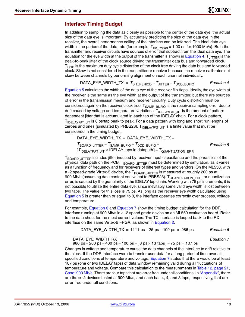
Receiver Interface Dynamic Timing
XAPP855 (v10) October 13 2006 wwwxilinxcom 18
R
Interface Timing Budget
In addition to sampling the data as closely as possible to the center of the data eye the actual size of the data eye is important By accurately predicting the size of the data eye in the receiver the overall performance ceiling of the interface can be inferred The ideal data eye width is the period of the data rate (for example TBit_Period = 100 ns for 1000 Mbs) Both the transmitter and receiver circuits have sources of error that subtract from the ideal data eye The equation for the eye width at the output of the transmitter is shown in Equation 4 TJITTER is the peak-to-peak jitter of the clock source driving the transmitter data bus and forwarded clock TDCD is the maximum duty cycle distortion of the clock tree driving the data bus and forwarded clock Skew is not considered in the transmitter or receiver because the receiver calibrates out skew between channels by performing alignment on each channel individually
Equation 4
Equation 5 calculates the width of the data eye at the receiver flip-flops Ideally the eye width at the receiver is the same as the eye width at the output of the transmitter but there are sources of error in the transmission medium and receiver circuitry Duty cycle distortion must be considered again on the receiver clock tree TSAMP_BUFIO is the receiver sampling error due to drift caused by voltage and temperature variations TIDELAYPAT_JIT is the amount of pattern dependent jitter that is accumulated in each tap of the IDELAY chain For a clock pattern TIDELAYPAT_JIT is 0 pstap peak to peak For a data pattern with long and short run lengths of zeroes and ones (simulated by PRBS23) TIDELAYPAT_JIT is a finite value that must be considered in the timing budget
Equation 5
TBOARD_JITTER includes jitter induced by receiver input capacitance and the parasitics of the physical data path on the PCB TBOARD_JITTER must be determined by simulation as it varies as a function of frequency and for receivers of different types and vendors On the ML550 with a -2 speed-grade Virtex-5 device the TBOARD_JITTER is measured at roughly 200 ps at 900 Mbs (assuming data content equivalent to PRBS23) TQUANTIZATION_ERR or quantization error is caused by the granularity of the IDELAY tap chain Working with 75 ps increments it is not possible to utilize the entire data eye since inevitably some valid eye width is lost between two taps The value for this loss is 75 ps As long as the receiver eye width calculated using Equation 5 is greater than or equal to 0 the interface operates correctly over process voltage and temperature
For example Equation 6 and Equation 7 show the timing budget calculation for the DDR interface running at 900 Mbs in a -2 speed grade device on an ML550 evaluation board Refer to the data sheet for the most current values The TX interface is looped back to the RX interface on the same Virtex-5 FPGA as shown in Equation 2
Equation 6
Equation 7
Changes in voltage and temperature cause the data channels of the interface to drift relative to the clock If the DDR interface were to transfer user data for a long period of time over all specified conditions of temperature and voltage Equation 7 states that there would be at least 107 ps (one or two IDELAY taps) of data window remaining valid during all fluctuations of temperature and voltage Compare this calculation to the measurements in Table 12 page 21 Case 900 Mbs There are four taps that are error free under all conditions In ldquoAppendixrdquo there are three -2 devices tested at 900 Mbs and each has 4 4 and 3 taps respectively that are error free under all conditions
DATA_EYE_WIDTH_TX TBIT_PERIOD TJITTERndash TDCD_BUFIOndash=
DATA_EYE_WIDTH_RX DATA_EYE_WIDTH_TX
TBOARD_JITTER
ndash
TSAMP_BUFIOndash TDCD_BUFIOndash
TIDELAYPAT_JIT IDELAY taps in datapathtimes[ ]ndash
TQUANTIZATION_ERRndash
=
DATA_EYE_WIDTH_TX 1111 ps 25 psndash 100 psndash 986 ps= =
DATA_EYE_WIDTH_RX986 ps 200 psndash 400 psndash 100 psndash 8 ps 13 tapstimes[ ] 75 ps 107 ps=ndashndash
=
Interface Characterization
XAPP855 (v10) October 13 2006 wwwxilinxcom 19
R
At a given temperature and voltage setting the data valid window is much larger because there is no drift when temperature and voltage are constant The size of the data valid window under constant conditions is 107 ps + TSAMP_BUFIO which in this case is at least 507 ps (six or seven IDELAY taps) Compare this calculation to the measurements of any single condition in Table 12 Case 900 Mbs In the worst case (ndash5 supply) there are 7 taps that are error free
Equation 8 and Equation 9 show the same timing budget calculation for the DDR interface running at 10 Gbs in a -2 speed grade device on an ML550 Evaluation Board
Equation 8
Equation 9
Equation 9 predicts that no data window remains valid during all specified fluctuations of temperature and voltage (compare to Table 12 Case 1000 Mbs) In ldquoAppendixrdquo there are three -2 devices tested at 1000 Mbs and each has 1 3 and 1 taps respectively that are error free under all conditions This data rate and device combination are very marginal cases
To operate at 10 Gbs the DDR interface requires additional circuitry to track out voltage-temperature variations in real-time (see XAPP860 16-channel DDR LVDS Interface with Real-time Window Monitoring for a DDR Interface with real-time window monitoring) If the voltage-temperature variations are removed from the picture the predicted data valid window is ndash120 ps + TSAMP_BUFIO which in this case is at least 280 ps (3 or 4 taps) Compare this calculation to the measurements of any single condition in Table 18 page 34 There are at least four error-free taps in all conditions
Interface Characterization
By following the procedure illustrated in Figure 13 page 15 the bit-alignment algorithm should never insert more than approximately 15 bit times of delay on the data channels The fewest number of delay taps should be used in the datapath because they produce a finite amount of degradation (TIDELAYPAT_JIT) The worst-case initial timing for the algorithm occurs when the clock samples just before the data transitions as in the 600 Mbs case in Figure 12 page 14 The algorithm must move all the way through the first eye to find the first transition (1 bit time) and then move halfway into the next eye to center the sampling point (05 bit time) This process produces a worst-case total delay insertion of 15 bit times
The actual performance of the bit-alignment algorithm is characterized as a function of data rate in Figure 15 page 20 For all data rates the expectation is that the tap settings of all 16 channels in the DDR receiver do not exceed approximately 15 bit times of delay Both the maximum and minimum tap setting of all 16 channels is recorded for each data rate This graph only shows the data for a single device Comparing the 15 bit time mask to the actual settings it is clear that the algorithm remains within the 15 bit time limit At 13 Gbs the tap setting actually exceeds the mask by one tap (a negligible violation)
DATA_EYE_WIDTH_TX 1000 ps 25 psndash 100 psndash 875 ps= =
DATA_EYE_WIDTH_RX 875 ps 300 psndash400 ps 100 psndash
ndash8 ps 15 tapstimes[ ] 75 ps 120 psndash=ndashndash
=
Interface Characterization
XAPP855 (v10) October 13 2006 wwwxilinxcom 20
R
The maximum and minimum tap settings in Figure 15 generally stay within 3 to 4 taps of each other except in the case of 640 Mbs and 1300 Mbs data rates These data rates are seams in the inherent timing At data rates below 640 Mbs the tap settings are in the range of 30 taps and at data rates above 640 Mbs the tap settings are in the range of 12 taps Referring back to Figure 12 page 14 it is clear why this seam occurs As the data rate increases past 600 Mbs the initial sampling point of the inherent timing moves into a different data eye creating a different starting point for the algorithm At 640 Mbs some of the 16 channels start in one eye while other channels start in the other eye Fortunately this is not an issue because the single bit time of difference between the channels is resolved using bitslip
Referring back to Figure 8 page 9 the clock channel goes through an IDELAY block with a default value of 0 Once the data rate is chosen for a given design this initial IDELAY value can be changed to a non-zero value to achieve more favorable inherent timing For example a design running at 620 Mbs can use 30 IDELAY taps on the delay channels each contributing a certain amount of jitter to the timing budget calculation By setting the initial clock delay to 5 taps the inherent timing moves across the seam shown in the 600 Mbs range of Figure 15 causing the data channels to only use about 12 IDELAY taps Only spectrally rich data patterns accumulate jitter in the IDELAY tap chain so the clock IDELAY can be set to any value without diminishing the timing budget This optimization is entirely optional and can be done once the design is running in hardware
The DDR receiver is designed to remove skew between channels by aligning each channel individually The ML550 board on which this reference design is characterized is designed to have minimal skew between channels However there is clearly a finite amount of skew between channels due to clock skew in the TX and RX BUFIO networks package skew and trace length tolerance on the ML550 board Table 11 page 21 shows how the bit-alignment algorithm sets the delay for each channel differently to compensate for skew between channels The table captures the range of settings among the 16 channels at specific data rates for a -2 device If there were additional skew among the 16 channels then the tap setting range would be larger to compensate for it The algorithm is designed such that skew between channels should not diminish the performance of the interface The range of tap settings differs for different devices and speed grades but the magnitude should be approximately the same
Figure 15 Bit-Alignment Algorithm Performance
60
50
40
30
20
10
0200 400 600 800 1000 1200 1400 1600
Data Rate (Mbs)
Del
ay T
ap U
tiliz
atio
n HW Measurement (Min)HW Measurement (Max)15 Bit Time Mask
X855_15_072406
Interface Characterization
XAPP855 (v10) October 13 2006 wwwxilinxcom 21
R
Since the receiver alignment logic only runs once immediately after reset the resulting dynamic timing must be adequate to ensure error-free operation over the specified voltage and temperature variations that can occur over time The data-valid window at the receiver input must be wide enough to withstand these variations (receiver drift) Table 12 page 21 shows the data-valid window at the ISERDES registers in the DDR receiver The eyes shown are collective eyes of all 16 channels The BERT testbench configuration loops back the DDR transmitter to the DDR receiver Using pattern generators and error detectors programmed to send and receive a pseudorandom bit sequence (PRBS23) the width of the data-valid window is evaluated using pseudorandom data that closely resembles real user data
Table 11 Tap Setting Range For Various Data Rates Measured on a -2 Device
Data Rate (Mbs) Tap Setting Range Compensated Skew
500 31ndash34 4 taps
600 28ndash30 3 taps
700 10ndash12 3 taps
800 11ndash13 3 taps
900 11ndash13 3 taps
1000 13ndash15 3 taps
1100 13ndash15 3 taps
1200 14ndash15 2 taps
Table 12 Measurement of Receiver Drift under Extreme Conditions for Multiple Data Rates
ConditionIODELAY Taps (1)
ndash8 ndash7 ndash6 ndash5 ndash4 ndash3 ndash2 ndash1 0 +1 +2 +3 +4 +5 +6 +7 +8
Case 800 Mbs
25degC Nom Supplies F F F P P P P P C P P P P P F F F
0degC Nom Supplies F F F P P P P P P P P P P P F F F
85degC Nom Supplies F F F P P P P P P P P P P P F F F
25degC +5 Supplies F P P P P P P P P P P P F F F F F
0degC +5 Supplies F P P P P P P P P P P P F F F F F
85degC +5 Supplies F P P P P P P P P P P P F F F F F
25degC ndash5 Supplies F F F F F F P P P P P P P P P F F
0degC ndash5 Supplies F F F F F F P P P P P P P P P P F
85degC ndash5 Supplies F F F F F P P P P P P P P P P F F
CONCLUSION Error free under all conditions when calibrated under nominal conditions to position C
Interface Characterization
XAPP855 (v10) October 13 2006 wwwxilinxcom 22
R
Case 900 Mbs
25degC Nom Supplies F F F F P P P P C P P P P F F F F
0degC Nom Supplies F F F F P P P P P P P P P F F F F
85degC Nom Supplies F F F F P P P P P P P P F F F F F
25degC +5 Supplies F F P P P P P P P P P F F F F F F
0degC +5 Supplies F F P P P P P P P P P F F F F F F
85degC +5 Supplies F F P P P P P P P P P F F F F F F
25degC ndash5 Supplies F F F F F F F P P P P P P P P F F
0degC ndash5 Supplies F F F F F F F P P P P P P P P F F
85degC ndash5 Supplies F F F F F F F P P P P P P P F F F
CONCLUSION Error free under all conditions when calibrated under nominal conditions to position C
Case 1000 Mbs
25degC Nom Supplies F F F F F P P P C P P P F F F F F
0degC Nom Supplies F F F F F P P P P P P P F F F F F
85degC Nom Supplies F F F F F P P P P P P P F F F F F
25degC +5 Supplies F F F P P P P P P P F F F F F F F
0degC +5 Supplies F F F P P P P P P P F F F F F F F
85degC +5 Supplies F F F P P P P P P P P F F F F F F
25degC ndash5 Supplies F F F F F F F F P P P P P P F F F
0degC ndash5 Supplies F F F F F F F F P P P P P P F F F
85degC ndash5 Supplies F F F F F F F F P P P P P P F F F
CONCLUSION Error free under all conditions when calibrated under nominal conditions to position C
Case 1100 Mbs
25degC Nom Supplies F F F F F P P P C P F F F F F F F
0degC Nom Supplies F F F F F P P P P P F F F F F F F
85degC Nom Supplies F F F F F P P P P P F F F F F F F
25degC +5 Supplies F F F P P P P P P F F F F F F F F
0degC +5 Supplies F F F P P P P P P F F F F F F F F
85degC +5 Supplies F F F P P P P P P F F F F F F F F
25degC ndash5 Supplies F F F F F F F F P P P P F F F F F
0degC ndash5 Supplies F F F F F F F F P P P P F F F F F
85degC ndash5 Supplies F F F F F F F F P P P P F F F F F
CONCLUSION Error free under all conditions when calibrated under nominal conditions to position C
Table 12 Measurement of Receiver Drift under Extreme Conditions for Multiple Data Rates (Continued)
ConditionIODELAY Taps (1)
ndash8 ndash7 ndash6 ndash5 ndash4 ndash3 ndash2 ndash1 0 +1 +2 +3 +4 +5 +6 +7 +8
Interface Characterization
XAPP855 (v10) October 13 2006 wwwxilinxcom 23
R
In all test cases shown in Table 12 page 21 the bit-align machine accurately places the sampling point in the center of the data eye (indicated by the C in each test case) In the 1100 Mbs case the bit-align machine places the sampling point slightly off center This slight inaccuracy occurs when the center of a real data pattern diverges from the center of the training pattern The electrical behavior of different data patterns is discussed below
After the dynamic timing is established for a given test case under nominal conditions the device is subjected to extremes of temperature and voltage to stress the receiver timing At data rates of 1100 Mbs and below the dynamic timing established after reset under nominal conditions is sufficient to meet timing over all specified extreme conditions (the column with the C passes traffic error free under all conditions) At a data rate of 1200 Mbs the design operates correctly under nominal conditions but the data-valid window is not large enough to withstand the voltage variations For this particular transmission medium the 1200 Mbs case requires a real-time adjustment circuit that could track the center of the eye
The full datapath of the testbench consists of
TX rarr 5 FR-4 rarr SAMTEC QSE Conn rarr 12 Ribbon Cable rarr SAMTEC QSE Conn rarr 5 FR-4 rarr RX
For shorter transmission media higher performance can be achieved in accordance with the section ldquoInterface Timing Budgetrdquo page 18 Interface performance is not solely a question of the LVDS driver performance specification but rather a question of adequate timing margin to withstand production and environmental variations From Table 12 the total amount of variation experienced over temperature and voltage is roughly 375 ps (5 taps at 75 ps per tap) This number should be comparable to the specification for receiver sampling error (TSAMP_BUFIO) shown in the Virtex-5 Data Sheet
Case 1200 Mbs
25degC Nom Supplies F F F F F F P P C P F F F F F F F
0degC Nom Supplies F F F F F F P P P P F F F F F F F
85degC Nom Supplies F F F F F F P P P F F F F F F F F
25degC +5 Supplies F F F F P P P P F F F F F F F F F
0degC +5 Supplies F F F P P P P P F F F F F F F F F
85degC +5 Supplies F F F F P P P P F F F F F F F F F
25degC ndash5 Supplies F F F F F F F F F P P P F F F F F
0degC ndash5 Supplies F F F F F F F F F P P P F F F F F
85degC ndash5 Supplies F F F F F F F F F P P F F F F F F
CONCLUSION Errors caused by plusmn5 variations in supply voltages
Notes 1 Where 0 is the reference tap determined by the bit-align machine under nominal conditions at 25degC2 P = Error-free transmission F = Error in transmission C = IODELAY tap position selected by bit-align machine under nominal conditions at 25degC3 Device under test is -2 speed grade
Table 12 Measurement of Receiver Drift under Extreme Conditions for Multiple Data Rates (Continued)
ConditionIODELAY Taps (1)
ndash8 ndash7 ndash6 ndash5 ndash4 ndash3 ndash2 ndash1 0 +1 +2 +3 +4 +5 +6 +7 +8
Interface Characterization
XAPP855 (v10) October 13 2006 wwwxilinxcom 24
R
Pattern Dependence of Receiver Performance
Different types of data patterns have different electrical signatures (rise and fall times jitter eye symmetry etc) A pattern with very narrow spectral content (such as a clock pattern) moves very favorably through the link because the receiver frequency response has little effect on the signal integrity However a pattern with wide spectral content (such as real data and pseudorandom patterns) stresses the links frequency response If the frequency response is not flat across the entire spectrum of the data content then the signal integrity is degraded as a result The amount of degradation measured is shown in Table 13 page 25 The DDR transmitter is looped back to the DDR receiver and different patterns are programmed to traverse the link Performance is assessed by evaluating the integrity of those patterns in the receiver
PRBS7 is a pseudorandom data pattern with a maximum run length of seven consecutive zeroes or ones PRBS15 is defined as having a maximum run length of fifteen consecutive zeroes or ones These limitations on run lengths limit the spectral content of the pattern A PRBS15 pattern has greater spectral content than a PRBS7 pattern and therefore is a more strenuous test for the link PRBS29 is the most strenuous test in Table 13 A clock pattern is effectively a PRBS1
As predicted Table 13 shows that there is more degradation for data patterns with more spectral content At 1000 Mbs and below the data eye closure is symmetrical Symmetrical eye closure is desired because it does not change the center of the eye as determined by the bit-alignment algorithm Above 1000 Mbs the eye closure becomes more asymmetrical causing the center of the data eye to diverge from the calibrated center (by only 1 tap)
In every data rate shown in Table 13 all significant pattern-dependent degradation is caused between PRBS1 (clock pat) and PRBS15 Between PRBS15 and PRBS29 there is no additional degradation recorded in any of the measurements
Interface Characterization
XAPP855 (v10) October 13 2006 wwwxilinxcom 25
R
Table 13 Link Performance for Various Types of Data Measured on a -2 Device
PatternIODELAY Taps (1)
ndash8 ndash7 ndash6 ndash5 ndash4 ndash3 ndash2 ndash1 0 +1 +2 +3 +4 +5 +6 +7 +8 +9
Case 600 Mbs
Clock Pat (0101) P P P P P P P P C P P P P P P P P P
Training Pat (0x2C) P P P P P P P P C P P P P P P P P F
PRBS7 P P P P P P P P C P P P P P P P P F
PRBS15 F P P P P P P P C P P P P P P P F F
PRBS23 F P P P P P P P C P P P P P P P F F
PRBS29 F P P P P P P P C P P P P P P P F F
Case 800 Mbs
Clock Pat (0101) F F P P P P P P C P P P P P P F F F
Training Pat (0x2C) F F P P P P P P C P P P P P P F F F
PRBS7 F F P P P P P P C P P P P P F F F F
PRBS15 F F F P P P P P C P P P P P F F F F
PRBS23 F F F P P P P P C P P P P P F F F F
PRBS29 F F F P P P P P C P P P P P F F F F
Case 1000 Mbs
Clock Pat (0101) F F F P P P P P C P P P P P F F F F
Training Pat (0x2C) F F F P P P P P C P P P P F F F F F
PRBS7 F F F F P P P P C P P P F F F F F F
PRBS15 F F F F F P P P C P P P F F F F F F
PRBS23 F F F F F P P P C P P P F F F F F F
PRBS29 F F F F F P P P C P P P F F F F F F
Case 1200 Mbs
Clock Pat (0101) F F F F P P P P C P P P P F F F F F
Training Pat (0x2C) F F F F P P P P C P P P F F F F F F
PRBS7 F F F F F P P P C P F F F F F F F F
PRBS15 F F F F F F P P C F F F F F F F F F
PRBS23 F F F F F F P P C F F F F F F F F F
PRBS29 F F F F F F P P C F F F F F F F F F
Case 1400 Mbs
Clock Pat (0101) F F F F F F P P C P P P F F F F F F
Training Pat (0x2C) F F F F F P P P C P P F F F F F F F
PRBS7 F F F F F F F P C P F F F F F F F F
PRBS15 F F F F F F F P C F F F F F F F F F
PRBS23 F F F F F F F P C F F F F F F F F F
PRBS29 F F F F F F F P C F F F F F F F F F
Notes 1 Where 0 is the reference tap determined by the bit-align machine under nominal conditions at 25degC2 P = Error-free transmission F = Error in transmission C = IODELAY tap position selected by bit-align machine under nominal conditions at 25degC
Resetting the Interface
XAPP855 (v10) October 13 2006 wwwxilinxcom 26
R
Resetting the Interface
Several dependencies determine the order in which circuits should be reset in the interface The receiver cannot begin the alignment algorithm if the transmitter is not sending the training pattern The transmitter must be reset before the receiver and time must be allowed for the training pattern to propagate across the link before the receiver comes out of reset The receiver also cannot begin the alignment algorithm until IDELAYCTRL has recovered from reset which could takes hundreds of cycles The recommended reset timing for the interface is shown in Figure 16 This reset timing is implemented in the BERT testbench for this interface
The TX reset (RST_TX) is used to reset all TX circuitry and also IDELAYCTRL The IDELAYCTRL reset is asynchronous so driving it with RST_TX is acceptable The minimum pulse width of IDELAYCTRL reset is 50 ns (TIDELAYCTRL_RPW) For that reason resets are held High for 16 clock cycles The RX reset (RST_RX) is used to reset all RX circuitry and is asserted when the IDELAYCTRL READY flag goes High indicating that the IODELAY blocks are calibrated
The timing of the READY flag in Figure 16 is a potential hazard Most likely it is High during a TX reset because it takes many cycles for IDELAYCTRL to deassert the READY flag It is easy to make the mistake of resetting the receiver too early To avoid this hazard the RX reset should be asserted only after seeing a deassertion and reassertion of the READY flag
Conclusion Based on the design and characterization described in this document the 16-Channel DDR reference design operates to the performance targets in Table 14 under all conditions of process voltage and temperature However to meet these targets over voltage and temperature the timing budget must be guaranteed according to the analysis in ldquoInterface Timing Budgetrdquo See ldquoAppendixrdquo page 27 for further justification of the maximum performance recommendations in Table 14
Figure 16 Recommended Interface Reset Timing
RST_TX
IDELAYCTRLREADY
RST_RX
16 Cycles X855_16_072406
Table 14 Performance of 16-Channel DDR Interface
Speed Grade Maximum Performance
-1 800 Mbs
-2 900 Mbs
-3 10 Gbs(1)
Notes 1 To achieve higher performance (up to 125 Gbs) see 16-channel DDR LVDS Interface with Realtime
Window Monitoring for an example of a DDR interface with real-time window monitoring
Appendix
XAPP855 (v10) October 13 2006 wwwxilinxcom 27
R
Appendix Performance Characterization Data
Refer to ldquoInterface Characterizationrdquo page 19 for explanations about how to interpret the data in the ldquoAppendixrdquo These tables show collective data eyes for the entire interface over process voltage and temperature (PVT) Three devices from each speed grade were selected for this characterization
The calibrated center position of the eye (marked by the C in the tables below) varies slightly from channel to channel (due to small skews between channels) That range is referred to as center tap range Analysis of Table 16 page 28 through Table 20 page 40 shows that the center tap range for slow and fast parts differ significantly at the same data rate (because the BIT_ALIGN_MACHINE algorithm adjusts for differences in speed)
All data in the ldquoAppendixrdquo is collected using the BERT testbench shown in Figure 2 page 2 The data pattern is PRBS23 and the devicepackage is XC5VLX50T-FF1136 The transmission path for the cases shown in Table 16 through Table 20 is repeated for convenience
TX rarr 5 FR-4 rarr SAMTEC QSE Conn rarr 12 Ribbon Cable rarr SAMTEC QSE Conn rarr 5 FR-4 rarr RX
A summary of these characterization results is shown in Table 15 Each of the nine parts were tested at 800 900 1000 1100 and 1200 Mbs When the interface is error free on all channels under all extreme conditions of temperature and voltage the particular test case is designated by a P A test case is marked FAIL when the interface suffered errors on any channel under any particular condition of voltage and temperature
Table 15 Summary of Interface Characterization Results
Device (SN) Speed Grade 800 Mbs 900 Mbs 1000Mbs 1100 Mbs 1200 Mbs
2194 -1 P P P FAIL FAIL
2219 -1 P FAIL FAIL FAIL FAIL
2199 -1 P P FAIL FAIL FAIL
001 -2 P P FAIL P FAIL
002 -2 P P P P FAIL
003 -2 P P FAIL FAIL FAIL
004 -3 P P P P P
005 -3 P P P P P
006 -3 P P P P P
Appendix
XAPP855 (v10) October 13 2006 wwwxilinxcom 28
R
Table 16 Measurement of Receiver Drift under Extreme Conditions at 800 Mbs
ConditionIODELAY Taps (1)
ndash8 ndash7 ndash6 ndash5 ndash4 ndash3 ndash2 ndash1 0 +1 +2 +3 +4 +5 +6 +7 +8
SN 2194 Speed Grade -1
25degC Nom Supplies F F F P P P P P C P P P P F F F F
0degC Nom Supplies F F F P P P P P P P P P P F F F F
85degC Nom Supplies F F F F P P P P P P P P P F F F F
25degC +5 Supplies F F P P P P P P P P P P F F F F F
0degC +5 Supplies F F P P P P P P P P P P F F F F F
85degC +5 Supplies F F P P P P P P P P P P F F F F F
25degC ndash5 Supplies F F F F F F P P P P P P P P P F F
0degC ndash5 Supplies F F F F F F P P P P P P P P P F F
85degC ndash5 Supplies F F F F F F P P P P P P P P P F F
Center Tap Range Taps 11ndash12
CONCLUSION Error free under all conditions when calibrated under nominal conditions to position C
SN 2219 Speed Grade -1
25degC Nom Supplies F F F P P P P P C P P P F F F F F
0degC Nom Supplies F F F P P P P P P P P P F F F F F
85degC Nom Supplies F F F P P P P P P P P P F F F F F
25degC +5 Supplies F P P P P P P P P P P F F F F F F
0degC +5 Supplies F P P P P P P P P P P F F F F F F
85degC +5 Supplies F P P P P P P P P P P F F F F F F
25degC ndash5 Supplies F F F F F F P P P P P P P P F F F
0degC ndash5 Supplies F F F F F F F P P P P P P P F F F
85degC ndash5 Supplies F F F F F F P P P P P P P P F F F
Center Tap Range Taps 13ndash16
CONCLUSION Error free under all conditions when calibrated under nominal conditions to position C
SN 2199 Speed Grade -1
25degC Nom Supplies F F F P P P P P C P P P P F F F F
0degC Nom Supplies F F F P P P P P P P P P P F F F F
85degC Nom Supplies F F F P P P P P P P P P P F F F F
25degC +5 Supplies F P P P P P P P P P P P F F F F F
0degC +5 Supplies F P P P P P P P P P P P F F F F F
85degC +5 Supplies F P P P P P P P P P P P F F F F F
25degC ndash5 Supplies F F F F F F P P P P P P P P P F F
0degC ndash5 Supplies F F F F F F P P P P P P P P P F F
85degC ndash5 Supplies F F F F F F P P P P P P P P P F F
Center Tap Range Taps 10ndash12
CONCLUSION Error free under all conditions when calibrated under nominal conditions to position C
Appendix
XAPP855 (v10) October 13 2006 wwwxilinxcom 29
R
SN 001 Speed Grade -2
25degC Nom Supplies F F F P P P P P C P P P P F F F F
0degC Nom Supplies F F F P P P P P P P P P P F F F F
85degC Nom Supplies F F F P P P P P P P P P P F F F F
25degC +5 Supplies F P P P P P P P P P P P F F F F F
0degC +5 Supplies F P P P P P P P P P P F F F F F F
85degC +5 Supplies F P P P P P P P P P P P F F F F F
25degC ndash5 Supplies F F F F F P P P P P P P P P P F F
0degC ndash5 Supplies F F F F F P P P P P P P P P P F F
85degC ndash5 Supplies F F F F F P P P P P P P P P P F F
Center Tap Range Taps 10ndash12
CONCLUSION Error free under all conditions when calibrated under nominal conditions to position C
SN 002 Speed Grade -2
25degC Nom Supplies F F F P P P P P C P P P P F F F F
0degC Nom Supplies F F F P P P P P P P P P P F F F F
85degC Nom Supplies F F F P P P P P P P P P P F F F F
25degC +5 Supplies F P P P P P P P P P P P F F F F F
0degC +5 Supplies F P P P P P P P P P P P F F F F F
85degC +5 Supplies F F P P P P P P P P P P F F F F F
25degC ndash5 Supplies F F F F F P P P P P P P P P P F F
0degC ndash5 Supplies F F F F F P P P P P P P P P P F F
85degC ndash5 Supplies F F F F F P P P P P P P P P P F F
Center Tap Range Taps 10ndash12
CONCLUSION Error free under all conditions when calibrated under nominal conditions to position C
SN 003 Speed Grade -2
25degC Nom Supplies F F F P P P P P C P P P P F F F F
0degC Nom Supplies F F F P P P P P P P P P P F F F F
85degC Nom Supplies F F F P P P P P P P P P P F F F F
25degC +5 Supplies F P P P P P P P P P P P F F F F F
0degC +5 Supplies F P P P P P P P P P P F F F F F F
85degC +5 Supplies F P P P P P P P P P P P F F F F F
25degC ndash5 Supplies F F F F F F P P P P P P P P P F F
0degC ndash5 Supplies F F F F F F P P P P P P P P P F F
85degC ndash5 Supplies F F F F F F P P P P P P P P P F F
Center Tap Range Taps 11ndash13
CONCLUSION Error free under all conditions when calibrated under nominal conditions to position C
Table 16 Measurement of Receiver Drift under Extreme Conditions at 800 Mbs (Continued)
ConditionIODELAY Taps (1)
ndash8 ndash7 ndash6 ndash5 ndash4 ndash3 ndash2 ndash1 0 +1 +2 +3 +4 +5 +6 +7 +8
Appendix
XAPP855 (v10) October 13 2006 wwwxilinxcom 30
R
SN 004 Speed Grade -3
25degC Nom Supplies F F F P P P P P C P P P P F F F F
0degC Nom Supplies F F F P P P P P P P P P F F F F F
85degC Nom Supplies F F F P P P P P P P P P P F F F F
25degC +5 Supplies F P P P P P P P P P P P F F F F F
0degC +5 Supplies F P P P P P P P P P P P F F F F F
85degC +5 Supplies F F P P P P P P P P P P F F F F F
25degC ndash5 Supplies F F F F F P P P P P P P P P F F F
0degC ndash5 Supplies F F F F F P P P P P P P P P F F F
85degC ndash5 Supplies F F F F F P P P P P P P P P F F F
Center Tap Range Taps 8ndash9 23ndash24
CONCLUSION Error free under all conditions when calibrated under nominal conditions to position C
SN 005 Speed Grade -3
25degC Nom Supplies F F P P P P P P C P P P P F F F F
0degC Nom Supplies F F P P P P P P P P P P P F F F F
85degC Nom Supplies F F F P P P P P P P P P P P F F F
25degC +5 Supplies F P P P P P P P P P P P F F F F F
0degC +5 Supplies F P P P P P P P P P P P F F F F F
85degC +5 Supplies F P P P P P P P P P P P F F F F F
25degC ndash5 Supplies F F F F P P P P P P P P P P P F F
0degC ndash5 Supplies F F F F P P P P P P P P P P P F F
85degC ndash5 Supplies F F F F P P P P P P P P P P P F F
Center Tap Range Taps 9ndash10
CONCLUSION Error free under all conditions when calibrated under nominal conditions to position C
SN 006 Speed Grade -3
25degC Nom Supplies F F P P P P P P C P P P P F F F F
0degC Nom Supplies F F P P P P P P P P P P P F F F F
85degC Nom Supplies F F F P P P P P P P P P P F F F F
25degC +5 Supplies F P P P P P P P P P P P F F F F F
0degC +5 Supplies F P P P P P P P P P P P F F F F F
85degC +5 Supplies F F P P P P P P P P P P F F F F F
25degC ndash5 Supplies F F F P P P P P P P P P P P F F F
0degC ndash5 Supplies F F F P P P P P P P P P P P F F F
85degC ndash5 Supplies F F F F F P P P P P P P P P F F F
Center Tap Range Taps 8ndash9 23ndash24
CONCLUSION Error free under all conditions when calibrated under nominal conditions to position C
Notes 1 IODELAY taps where 0 is the reference tap determined by the bit align machine at nominal voltage and 25degC2 P = Error-free transmission F = Error in transmission C = IODELAY tap position selected by bit-align machine under nominal conditions at 25degC
Table 16 Measurement of Receiver Drift under Extreme Conditions at 800 Mbs (Continued)
ConditionIODELAY Taps (1)
ndash8 ndash7 ndash6 ndash5 ndash4 ndash3 ndash2 ndash1 0 +1 +2 +3 +4 +5 +6 +7 +8
Appendix
XAPP855 (v10) October 13 2006 wwwxilinxcom 31
R
Table 17 Measurement of Receiver Drift under Extreme Conditions at 900 Mbs
ConditionIODELAY Taps (1)
ndash8 ndash7 ndash6 ndash5 ndash4 ndash3 ndash2 ndash1 0 +1 +2 +3 +4 +5 +6 +7 +8
SN 2194 Speed Grade -1
25degC Nom Supplies F F F F F P P P C P P P F F F F F
0degC Nom Supplies F F F F F P P P P P P P F F F F F
85degC Nom Supplies F F F F F P P P P P P P P F F F F
25degC +5 Supplies F F F P P P P P P P P F F F F F F
0degC +5 Supplies F F F P P P P P P P P F F F F F F
85degC +5 Supplies F F F P P P P P P P P F F F F F F
25degC ndash5 Supplies F F F F F F F P P P P P P P F F F
0degC ndash5 Supplies F F F F F F F P P P P P P P F F F
85degC ndash5 Supplies F F F F F F F P P P P P P P F F F
Center Tap Range Taps 11ndash12
CONCLUSION Error free under all conditions when calibrated under nominal conditions to position C
SN 2219 Speed Grade -1
25degC Nom Supplies F F F F F P P P C P P P F F F F F
0degC Nom Supplies F F F F F P P P P P P P F F F F F
85degC Nom Supplies F F F F F P P P P P P P F F F F F
25degC +5 Supplies F F F P P P P P P P F F F F F F F
0degC +5 Supplies F F F P P P P P P P F F F F F F F
85degC +5 Supplies F F F P P P P P P P F F F F F F F
25degC ndash5 Supplies F F F F F F F F F P P P P P F F F
0degC ndash5 Supplies F F F F F F F F F P P P P P F F F
85degC ndash5 Supplies F F F F F F F F P P P P P P F F F
Center Tap Range Taps 12ndash15
CONCLUSION Errors caused by ndash5 variation in supply voltage
SN 2199 Speed Grade -1
25degC Nom Supplies F F F F F P P P C P P P F F F F F
0degC Nom Supplies F F F F F P P P P P P P F F F F F
85degC Nom Supplies F F F F F P P P P P P P F F F F F
25degC +5 Supplies F F F P P P P P P P P F F F F F F
0degC +5 Supplies F F F P P P P P P P P F F F F F F
85degC +5 Supplies F F F P P P P P P P P F F F F F F
25degC ndash5 Supplies F F F F F F F F P P P P P P F F F
0degC ndash5 Supplies F F F F F F F F P P P P P P F F F
85degC ndash5 Supplies F F F F F F F F P P P P P P F F F
Center Tap Range Taps 10ndash12
CONCLUSION Error free under all conditions when calibrated under nominal conditions to position C
Appendix
XAPP855 (v10) October 13 2006 wwwxilinxcom 32
R
SN 001 Speed Grade -2
25degC Nom Supplies F F F F P P P P C P P P P F F F F
0degC Nom Supplies F F F F P P P P P P P P P F F F F
85degC Nom Supplies F F F F F P P P P P P P P F F F F
25degC +5 Supplies F F P P P P P P P P P F F F F F F
0degC +5 Supplies F F P P P P P P P P P F F F F F F
85degC +5 Supplies F F F P P P P P P P P P F F F F F
25degC ndash5 Supplies F F F F F F F P P P P P P P F F F
0degC ndash5 Supplies F F F F F F F P P P P P P P F F F
85degC ndash5 Supplies F F F F F F F P P P P P P P F F F
Center Tap Range Taps 9ndash11
CONCLUSION Error free under all conditions when calibrated under nominal conditions to position C
SN 002 Speed Grade -2
25degC Nom Supplies F F F F P P P P C P P P P F F F F
0degC Nom Supplies F F F F P P P P P P P P F F F F F
85degC Nom Supplies F F F F F P P P P P P P P F F F F
25degC +5 Supplies F F F P P P P P P P P F F F F F F
0degC +5 Supplies F F F P P P P P P P P F F F F F F
85degC +5 Supplies F F F P P P P P P P P P F F F F F
25degC ndash5 Supplies F F F F F F F P P P P P P P F F F
0degC ndash5 Supplies F F F F F F F P P P P P P P F F F
85degC ndash5 Supplies F F F F F F F P P P P P P P F F F
Center Tap Range Taps 10ndash12
CONCLUSION Error free under all conditions when calibrated under nominal conditions to position C
SN 003 Speed Grade -2
25degC Nom Supplies F F F F F P P P C P P P P F F F F
0degC Nom Supplies F F F F F P P P P P P P P F F F F
85degC Nom Supplies F F F F F P P P P P P P P F F F F
25degC +5 Supplies F F P P P P P P P P P F F F F F F
0degC +5 Supplies F F P P P P P P P P P F F F F F F
85degC +5 Supplies F F F P P P P P P P P F F F F F F
25degC ndash5 Supplies F F F F F F F P P P P P P P F F F
0degC ndash5 Supplies F F F F F F F F P P P P P P F F F
85degC ndash5 Supplies F F F F F F F P P P P P P P F F F
Center Tap Range Taps 11ndash13
CONCLUSION Error free under all conditions when calibrated under nominal conditions to position C
Table 17 Measurement of Receiver Drift under Extreme Conditions at 900 Mbs (Continued)
ConditionIODELAY Taps (1)
ndash8 ndash7 ndash6 ndash5 ndash4 ndash3 ndash2 ndash1 0 +1 +2 +3 +4 +5 +6 +7 +8
Appendix
XAPP855 (v10) October 13 2006 wwwxilinxcom 33
R
SN 004 Speed Grade -3
25degC Nom Supplies F F F F P P P P C P P P P F F F F
0degC Nom Supplies F F F P P P P P P P P P P F F F F
85degC Nom Supplies F F F F P P P P P P P P P F F F F
25degC +5 Supplies F F F P P P P P P P P P F F F F F
0degC +5 Supplies F F F P P P P P P P P P F F F F F
85degC +5 Supplies F F F P P P P P P P P P F F F F F
25degC ndash5 Supplies F F F F F F P P P P P P P P F F F
0degC ndash5 Supplies F F F F F F P P P P P P P P F F F
85degC ndash5 Supplies F F F F F F P P P P P P P P F F F
Center Tap Range Taps 7ndash8
CONCLUSION Error free under all conditions when calibrated under nominal conditions to position C
SN 005 Speed Grade ndash3
25degC Nom Supplies F F F P P P P P C P P P P F F F F
0degC Nom Supplies F F F P P P P P P P P P P F F F F
85degC Nom Supplies F F F F P P P P P P P P P F F F F
25degC +5 Supplies F F P P P P P P P P P P F F F F F
0degC +5 Supplies F F P P P P P P P P P P F F F F F
85degC +5 Supplies F F F P P P P P P P P P F F F F F
25degC ndash5 Supplies F F F F F F P P P P P P P P F F F
0degC ndash5 Supplies F F F F F P P P P P P P P P F F F
85degC ndash5 Supplies F F F F F F P P P P P P P P F F F
Center Tap Range Taps 9ndash10
CONCLUSION Error free under all conditions when calibrated under nominal conditions to position C
SN 006 Speed Grade -3
25degC Nom Supplies F F F F P P P P C P P P P F F F F
0degC Nom Supplies F F F F P P P P P P P P P F F F F
85degC Nom Supplies F F F F P P P P P P P P P F F F F
25degC +5 Supplies F F P P P P P P P P P P F F F F F
0degC +5 Supplies F F P P P P P P P P P P F F F F F
85degC +5 Supplies F F F P P P P P P P P P F F F F F
25degC ndash5 Supplies F F F F F P P P P P P P P P F F F
0degC ndash5 Supplies F F F F F P P P P P P P P P F F F
85degC ndash5 Supplies F F F F F F P P P P P P P P F F F
Center Tap Range Taps 7ndash8
CONCLUSION Error free under all conditions when calibrated under nominal conditions to position C
Notes 1 IODELAY taps where 0 is the reference tap determined by the bit align machine at nominal voltage and 25degC2 P = Error-free transmission F = Error in transmission C = IODELAY tap position selected by bit-align machine under nominal conditions at 25degC
Table 17 Measurement of Receiver Drift under Extreme Conditions at 900 Mbs (Continued)
ConditionIODELAY Taps (1)
ndash8 ndash7 ndash6 ndash5 ndash4 ndash3 ndash2 ndash1 0 +1 +2 +3 +4 +5 +6 +7 +8
Appendix
XAPP855 (v10) October 13 2006 wwwxilinxcom 34
R
Table 18 Measurement of Receiver Drift under Extreme Conditions at 1000 Mbs
ConditionIODELAY Taps (1)
ndash8 ndash7 ndash6 ndash5 ndash4 ndash3 ndash2 ndash1 0 +1 +2 +3 +4 +5 +6 +7 +8
SN 2194 Speed Grade -1
25degC Nom Supplies F F F F F P P P C P P F F F F F F
0degC Nom Supplies F F F F F P P P P P P F F F F F F
85degC Nom Supplies F F F F F P P P P P P F F F F F F
25degC +5 Supplies F F F P P P P P P P F F F F F F F
0degC +5 Supplies F F F P P P P P P P F F F F F F F
85degC +5 Supplies F F F F P P P P P P F F F F F F F
25degC ndash5 Supplies F F F F F F F F P P P P P F F F F
0degC ndash5 Supplies F F F F F F F F P P P P P F F F F
85degC ndash5 Supplies F F F F F F F F P P P P P F F F F
Center Tap Range Taps 12ndash13
CONCLUSION Error free under all conditions when calibrated under nominal conditions to position C
SN 2219 Speed Grade -1
25degC Nom Supplies F F F F F F P P C P P F F F F F F
0degC Nom Supplies F F F F F F P P P P P F F F F F F
85degC Nom Supplies F F F F F F P P P P P F F F F F F
25degC +5 Supplies F F F P P P P P P F F F F F F F F
0degC +5 Supplies F F F P P P P P P F F F F F F F F
85degC +5 Supplies F F F F P P P P P F F F F F F F F
25degC ndash5 Supplies F F F F F F F F F P P P P F F F F
0degC ndash5 Supplies F F F F F F F F F F P P P F F F F
85degC ndash5 Supplies F F F F F F F F F P P P P F F F F
Center Tap Range Taps 14ndash17
CONCLUSION Errors caused by ndash5 variation in supply voltage
SN 2199 Speed Grade -1
25degC Nom Supplies F F F F F F P P C P P F F F F F F
0degC Nom Supplies F F F F F F P P P P P F F F F F F
85degC Nom Supplies F F F F F F P P P P P F F F F F F
25degC +5 Supplies F F F F P P P P P P F F F F F F F
0degC +5 Supplies F F F F P P P P P P F F F F F F F
85degC +5 Supplies F F F F P P P P P P F F F F F F F
25degC ndash5 Supplies F F F F F F F F F P P P P F F F F
0degC ndash5 Supplies F F F F F F F F F P P P P F F F F
85degC ndash5 Supplies F F F F F F F F F P P P P F F F F
Center Tap Range Taps 12ndash14
CONCLUSION Errors caused by ndash5 variation in supply voltage
Appendix
XAPP855 (v10) October 13 2006 wwwxilinxcom 35
R
SN 001 Speed Grade -2
25degC Nom Supplies F F F F F F P P C P P P F F F F F
0degC Nom Supplies F F F F F F P P P P P P F F F F F
85degC Nom Supplies F F F F F F P P P P P P F F F F F
25degC +5 Supplies F F F F P P P P P P F F F F F F F
0degC +5 Supplies F F F F P P P P P P F F F F F F F
85degC +5 Supplies F F F F P P P P P P P F F F F F F
25degC ndash5 Supplies F F F F F F F F F P P P P F F F F
0degC ndash5 Supplies F F F F F F F F F P P P P F F F F
85degC ndash5 Supplies F F F F F F F F F P P P P F F F F
Center Tap Range Taps 11ndash12
CONCLUSION Errors caused by ndash5 variation in supply voltage
SN 002 Speed Grade -2
25degC Nom Supplies F F F F F P P P C P P F F F F F F
0degC Nom Supplies F F F F F P P P P P P P F F F F F
85degC Nom Supplies F F F F F P P P P P P P F F F F F
25degC +5 Supplies F F F F P P P P P P F F F F F F F
0degC +5 Supplies F F F P P P P P P P F F F F F F F
85degC +5 Supplies F F F F P P P P P P P F F F F F F
25degC ndash5 Supplies F F F F F F F P P P P P P F F F F
0degC ndash5 Supplies F F F F F F F P P P P P P F F F F
85degC ndash5 Supplies F F F F F F F P P P P P P F F F F
Center Tap Range Taps 11ndash13
CONCLUSION Error free under all conditions when calibrated under nominal conditions to position C
SN 003 Speed Grade -2
25degC Nom Supplies F F F F F F P P C P P F F F F F F
0degC Nom Supplies F F F F F F P P P P P F F F F F F
85degC Nom Supplies F F F F F F P P P P P F F F F F F
25degC +5 Supplies F F F F P P P P P P F F F F F F F
0degC +5 Supplies F F F F P P P P P P F F F F F F F
85degC +5 Supplies F F F F P P P P P P F F F F F F F
25degC ndash5 Supplies F F F F F F F F F P P P P F F F F
0degC ndash5 Supplies F F F F F F F F F P P P P F F F F
85degC ndash5 Supplies F F F F F F F F F P P P P F F F F
Center Tap Range Taps 13ndash14
CONCLUSION Errors caused by ndash5 variation in supply voltage
Table 18 Measurement of Receiver Drift under Extreme Conditions at 1000 Mbs (Continued)
ConditionIODELAY Taps (1)
ndash8 ndash7 ndash6 ndash5 ndash4 ndash3 ndash2 ndash1 0 +1 +2 +3 +4 +5 +6 +7 +8
Appendix
XAPP855 (v10) October 13 2006 wwwxilinxcom 36
R
SN 004 Speed Grade -3
25degC Nom Supplies F F F F F P P P C P P P F F F F F
0degC Nom Supplies F F F F F P P P P P P P F F F F F
85degC Nom Supplies F F F F F P P P P P P P F F F F F
25degC +5 Supplies F F F P P P P P P P P F F F F F F
0degC +5 Supplies F F F P P P P P P P P F F F F F F
85degC +5 Supplies F F F F P P P P P P P P F F F F F
25degC ndash5 Supplies F F F F F F F P P P P P P F F F F
0degC ndash5 Supplies F F F F F F F P P P P P P F F F F
85degC ndash5 Supplies F F F F F F F P P P P P P P F F F
Center Tap Range Taps 9ndash10
CONCLUSION Error free under all conditions when calibrated under nominal conditions to position C
SN 005 Speed Grade -3
25degC Nom Supplies F F F F P P P P C P P P F F F F F
0degC Nom Supplies F F F F P P P P P P P P F F F F F
85degC Nom Supplies F F F F P P P P P P P P F F F F F
25degC +5 Supplies F F F P P P P P P P P F F F F F F
0degC +5 Supplies F F P P P P P P P P P F F F F F F
85degC +5 Supplies F F F P P P P P P P P F F F F F F
25degC ndash5 Supplies F F F F F F P P P P P P P P F F F
0degC ndash5 Supplies F F F F F F P P P P P P P P F F F
85degC ndash5 Supplies F F F F F F P P P P P P P F F F F
Center Tap Range Taps 11ndash12
CONCLUSION Error free under all conditions when calibrated under nominal conditions to position C
SN 006 Speed Grade -3
25degC Nom Supplies F F F F P P P P C P P P F F F F F
0degC Nom Supplies F F F F P P P P P P P P F F F F F
85degC Nom Supplies F F F F P P P P P P P P F F F F F
25degC +5 Supplies F F F P P P P P P P P F F F F F F
0degC +5 Supplies F F F P P P P P P P P F F F F F F
85degC +5 Supplies F F F P P P P P P P P F F F F F F
25degC ndash5 Supplies F F F F F F P P P P P P P F F F F
0degC ndash5 Supplies F F F F F F P P P P P P P F F F F
85degC ndash5 Supplies F F F F F F P P P P P P P F F F F
Center Tap Range Taps 9ndash10
CONCLUSION Error free under all conditions when calibrated under nominal conditions to position C
Notes 1 IODELAY taps where 0 is the reference tap determined by the bit align machine at nominal voltage and 25degC2 P = Error-free transmission F = Error in transmission C = IODELAY tap position selected by bit-align machine under nominal conditions at 25degC
Table 18 Measurement of Receiver Drift under Extreme Conditions at 1000 Mbs (Continued)
ConditionIODELAY Taps (1)
ndash8 ndash7 ndash6 ndash5 ndash4 ndash3 ndash2 ndash1 0 +1 +2 +3 +4 +5 +6 +7 +8
Appendix
XAPP855 (v10) October 13 2006 wwwxilinxcom 37
R
Table 19 Measurement of Receiver Drift under Extreme Conditions at 1100 Mbs
ConditionIODELAY Taps (1)
ndash8 ndash7 ndash6 ndash5 ndash4 ndash3 ndash2 ndash1 0 +1 +2 +3 +4 +5 +6 +7 +8
SN 2194 Speed Grade -1
25degC Nom Supplies F F F F F F P P C P P F F F F F F
0degC Nom Supplies F F F F F F P P P P P F F F F F F
85degC Nom Supplies F F F F F F P P P P P F F F F F F
25degC +5 Supplies F F F F P P P P P F F F F F F F F
0degC +5 Supplies F F F F P P P P P F F F F F F F F
85degC +5 Supplies F F F F P P P P P F F F F F F F F
25degC ndash5 Supplies F F F F F F F F F P P P F F F F F
0degC ndash5 Supplies F F F F F F F F F P P P F F F F F
85degC ndash5 Supplies F F F F F F F F F P P P F F F F F
Center Tap Range Taps 13ndash14
CONCLUSION Errors caused by ndash5 variation in supply voltage
SN 2219 Speed Grade -1
25degC Nom Supplies F F F F F F P P C P F F F F F F F
0degC Nom Supplies F F F F F F P P P P F F F F F F F
85degC Nom Supplies F F F F F F P P P P F F F F F F F
25degC +5 Supplies F F F F P P P P F F F F F F F F F
0degC +5 Supplies F F F F P P P P F F F F F F F F F
85degC +5 Supplies F F F F P P P P F F F F F F F F F
25degC ndash5 Supplies F F F F F F F F F F P P F F F F F
0degC ndash5 Supplies F F F F F F F F F F P P F F F F F
85degC ndash5 Supplies F F F F F F F F F P P P F F F F F
Center Tap Range Taps 6 15ndash17
CONCLUSION Errors caused by plusmn5 variation in supply voltage
SN 2199 Speed Grade -1
25degC Nom Supplies F F F F F F F P C P F F F F F F F
0degC Nom Supplies F F F F F F F P P P F F F F F F F
85degC Nom Supplies F F F F F F F P P P F F F F F F F
25degC +5 Supplies F F F F P P P P P F F F F F F F F
0degC +5 Supplies F F F F P P P P P F F F F F F F F
85degC +5 Supplies F F F F F P P P P F F F F F F F F
25degC ndash5 Supplies F F F F F F F F F F P P F F F F F
0degC ndash5 Supplies F F F F F F F F F F P P F F F F F
85degC ndash5 Supplies F F F F F F F F F F P P F F F F F
Center Tap Range Taps 13ndash15
CONCLUSION Errors caused by ndash5 variation in supply voltage
Appendix
XAPP855 (v10) October 13 2006 wwwxilinxcom 38
R
SN 001 Speed Grade -2
25degC Nom Supplies F F F F F F P P C P P F F F F F F
0degC Nom Supplies F F F F F F P P P P P F F F F F F
85degC Nom Supplies F F F F F F P P P P P F F F F F F
25degC +5 Supplies F F F F P P P P P F F F F F F F F
0degC +5 Supplies F F F F P P P P P F F F F F F F F
85degC +5 Supplies F F F F P P P P P F F F F F F F F
25degC ndash5 Supplies F F F F F F F F P P P P F F F F F
0degC ndash5 Supplies F F F F F F F F P P P P F F F F F
85degC ndash5 Supplies F F F F F F F F P P P P F F F F F
Center Tap Range Taps 12ndash13
CONCLUSION Error free under all conditions when calibrated under nominal conditions to position C
SN 002 Speed Grade -2
25degC Nom Supplies F F F F F P P P C P F F F F F F F
0degC Nom Supplies F F F F F P P P P P F F F F F F F
85degC Nom Supplies F F F F F F P P P P F F F F F F F
25degC +5 Supplies F F F F P P P P P F F F F F F F F
0degC +5 Supplies F F F P P P P P P F F F F F F F F
85degC +5 Supplies F F F F P P P P P F F F F F F F F
25degC ndash5 Supplies F F F F F F F F P P P P F F F F F
0degC ndash5 Supplies F F F F F F F F P P P P F F F F F
85degC ndash5 Supplies F F F F F F F F P P P P F F F F F
Center Tap Range Taps 13ndash14
CONCLUSION Error free under all conditions when calibrated under nominal conditions to position C
SN 003 Speed Grade -2
25degC Nom Supplies F F F F F F F P C P F F F F F F F
0degC Nom Supplies F F F F F F F P P P F F F F F F F
85degC Nom Supplies F F F F F F F P P P P F F F F F F
25degC +5 Supplies F F F F F P P P P F F F F F F F F
0degC +5 Supplies F F F F F P P P P F F F F F F F F
85degC +5 Supplies F F F F F P P P P F F F F F F F F
25degC ndash5 Supplies F F F F F F F F F F P P F F F F F
0degC ndash5 Supplies F F F F F F F F F F P P F F F F F
85degC ndash5 Supplies F F F F F F F F F P P P F F F F F
Center Tap Range Taps 14ndash16
CONCLUSION Errors caused by ndash5 variation in supply voltage
Table 19 Measurement of Receiver Drift under Extreme Conditions at 1100 Mbs (Continued)
ConditionIODELAY Taps (1)
ndash8 ndash7 ndash6 ndash5 ndash4 ndash3 ndash2 ndash1 0 +1 +2 +3 +4 +5 +6 +7 +8
Appendix
XAPP855 (v10) October 13 2006 wwwxilinxcom 39
R
SN 004 Speed Grade -3
25degC Nom Supplies F F F F F P P P C P P F F F F F F
0degC Nom Supplies F F F F F P P P P P P F F F F F F
85degC Nom Supplies F F F F F F P P P P P F F F F F F
25degC +5 Supplies F F F F P P P P P P F F F F F F F
0degC +5 Supplies F F F F P P P P P P F F F F F F F
85degC +5 Supplies F F F F P P P P P P F F F F F F F
25degC ndash5 Supplies F F F F F F F F P P P P F F F F F
0degC ndash5 Supplies F F F F F F F P P P P P F F F F F
85degC ndash5 Supplies F F F F F F F F P P P P P F F F F
Center Tap Range Taps 9ndash10
CONCLUSION Error free under all conditions when calibrated under nominal conditions to position C
SN 005 Speed Grade -3
25degC Nom Supplies F F F F F P P P C P P F F F F F F
0degC Nom Supplies F F F F F P P P P P P F F F F F F
85degC Nom Supplies F F F F F F P P P P P F F F F F F
25degC +5 Supplies F F F F P P P P P P F F F F F F F
0degC +5 Supplies F F F F P P P P P P F F F F F F F
85degC +5 Supplies F F F F P P P P P P F F F F F F F
25degC ndash5 Supplies F F F F F F F P P P P P P F F F F
0degC ndash5 Supplies F F F F F F F P P P P P P F F F F
85degC ndash5 Supplies F F F F F F F P P P P P P F F F F
Center Tap Range Taps 11ndash12
CONCLUSION Error free under all conditions when calibrated under nominal conditions to position C
SN 006 Speed Grade -3
25degC Nom Supplies F F F F F P P P C P P P F F F F F
0degC Nom Supplies F F F F F P P P P P P F F F F F F
85degC Nom Supplies F F F F F P P P P P P P F F F F F
25degC +5 Supplies F F F F P P P P P P P F F F F F F
0degC +5 Supplies F F F P P P P P P P F F F F F F F
85degC +5 Supplies F F F F P P P P P P P F F F F F F
25degC ndash5 Supplies F F F F F F P P P P P P P F F F F
0degC ndash5 Supplies F F F F F F P P P P P P P F F F F
85degC ndash5 Supplies F F F F F F F P P P P P P F F F F
Center Tap Range Taps 9ndash10
CONCLUSION Error free under all conditions when calibrated under nominal conditions to position C
Notes 1 IODELAY taps where 0 is the reference tap determined by the bit align machine at nominal voltage and 25degC2 P = Error-free transmission F = Error in transmission C = IODELAY tap position selected by bit-align machine under nominal conditions at 25degC
Table 19 Measurement of Receiver Drift under Extreme Conditions at 1100 Mbs (Continued)
ConditionIODELAY Taps (1)
ndash8 ndash7 ndash6 ndash5 ndash4 ndash3 ndash2 ndash1 0 +1 +2 +3 +4 +5 +6 +7 +8
Appendix
XAPP855 (v10) October 13 2006 wwwxilinxcom 40
R
Table 20 Measurement of Receiver Drift under Extreme Conditions at 1200 Mbs
ConditionIODELAY Taps (1)
ndash8 ndash7 ndash6 ndash5 ndash4 ndash3 ndash2 ndash1 0 +1 +2 +3 +4 +5 +6 +7 +8
SN 2194 Speed Grade -1
25degC Nom Supplies F F F F F F F P C F F F F F F F F
0degC Nom Supplies F F F F F F F P P F F F F F F F F
85degC Nom Supplies F F F F F F F P P F F F F F F F F
25degC +5 Supplies F F F F P P P P F F F F F F F F F
0degC +5 Supplies F F F F P P P P F F F F F F F F F
85degC +5 Supplies F F F F F P P P F F F F F F F F F
25degC ndash5 Supplies F F F F F F F F F P P F F F F F F
0degC ndash5 Supplies F F F F F F F F F F P F F F F F F
85degC ndash5 Supplies F F F F F F F F F P F F F F F F F
Center Tap Range Taps 13ndash15
CONCLUSION Errors caused by plusmn5 variation in supply voltage
SN 2219 Speed Grade -1
25degC Nom Supplies F F F F F F F F C F F F F F F F F
0degC Nom Supplies F F F F F F F P P F F F F F F F F
85degC Nom Supplies F F F F F F F F P F F F F F F F F
25degC +5 Supplies F F F F F P P P F F F F F F F F F
0degC +5 Supplies F F F F F P P P F F F F F F F F F
85degC +5 Supplies F F F F F F P P F F F F F F F F F
25degC ndash5 Supplies F F F F F F F F F F F F F F F F F
0degC ndash5 Supplies F F F F F F F F F F F F F F F F F
85degC ndash5 Supplies F F F F F F F F F F F F F F F F F
Center Tap Range Taps 6ndash7 16ndash17
CONCLUSION Errors caused by plusmn5 variation in supply voltage
SN 2199 Speed Grade -1
25degC Nom Supplies F F F F F F F P C F F F F F F F F
0degC Nom Supplies F F F F F F F P P F F F F F F F F
85degC Nom Supplies F F F F F F F F P F F F F F F F F
25degC +5 Supplies F F F F F P P P F F F F F F F F F
0degC +5 Supplies F F F F F P P P F F F F F F F F F
85degC +5 Supplies F F F F F P P P F F F F F F F F F
25degC ndash5 Supplies F F F F F F F F F F F F F F F F F
0degC ndash5 Supplies F F F F F F F F F F F F F F F F F
85degC ndash5 Supplies F F F F F F F F F F F F F F F F F
Center Tap Range Taps 13ndash15
CONCLUSION Errors caused by plusmn5 variation in supply voltage
Appendix
XAPP855 (v10) October 13 2006 wwwxilinxcom 41
R
SN 001 Speed Grade -2
25degC Nom Supplies F F F F F F F P C P F F F F F F F
0degC Nom Supplies F F F F F F F P P P F F F F F F F
85degC Nom Supplies F F F F F F F P P P F F F F F F F
25degC +5 Supplies F F F F F P P P P F F F F F F F F
0degC +5 Supplies F F F F P P P P P F F F F F F F F
85degC +5 Supplies F F F F F P P P P F F F F F F F F
25degC ndash5 Supplies F F F F F F F F F F P F F F F F F
0degC ndash5 Supplies F F F F F F F F F F P F F F F F F
85degC ndash5 Supplies F F F F F F F F F F P F F F F F F
Center Tap Range Taps 12ndash13
CONCLUSION Errors caused by ndash5 variation in supply voltage
SN 002 Speed Grade -2
25degC Nom Supplies F F F F F F P P C P F F F F F F F
0degC Nom Supplies F F F F F F P P P P F F F F F F F
85degC Nom Supplies F F F F F F F P P P F F F F F F F
25degC +5 Supplies F F F F P P P P F F F F F F F F F
0degC +5 Supplies F F F F P P P P F F F F F F F F F
85degC +5 Supplies F F F F F P P P F F F F F F F F F
25degC ndash5 Supplies F F F F F F F F P P P F F F F F F
0degC ndash5 Supplies F F F F F F F F P P P F F F F F F
85degC ndash5 Supplies F F F F F F F F F P P F F F F F F
Center Tap Range Taps 13ndash14
CONCLUSION Errors caused by plusmn5 variation in supply voltage
SN 003 Speed Grade -2
25degC Nom Supplies F F F F F F F P C F F F F F F F F
0degC Nom Supplies F F F F F F F P P F F F F F F F F
85degC Nom Supplies F F F F F F F F P F F F F F F F F
25degC +5 Supplies F F F F F P P P F F F F F F F F F
0degC +5 Supplies F F F F F P P P F F F F F F F F F
85degC +5 Supplies F F F F F F P P F F F F F F F F F
25degC ndash5 Supplies F F F F F F F F F F F F F F F F F
0degC ndash5 Supplies F F F F F F F F F F F F F F F F F
85degC ndash5 Supplies F F F F F F F F F F F F F F F F F
Center Tap Range Taps 14ndash15
CONCLUSION Errors caused by plusmn5 variation in supply voltage
Table 20 Measurement of Receiver Drift under Extreme Conditions at 1200 Mbs (Continued)
ConditionIODELAY Taps (1)
ndash8 ndash7 ndash6 ndash5 ndash4 ndash3 ndash2 ndash1 0 +1 +2 +3 +4 +5 +6 +7 +8
Appendix
XAPP855 (v10) October 13 2006 wwwxilinxcom 42
R
SN 004 Speed Grade -3
25degC Nom Supplies F F F F F F P P C P F F F F F F F
0degC Nom Supplies F F F F F P P P P P F F F F F F F
85degC Nom Supplies F F F F F F P P P P F F F F F F F
25degC +5 Supplies F F F F P P P P P F F F F F F F F
0degC +5 Supplies F F F F P P P P P F F F F F F F F
85degC +5 Supplies F F F F F P P P P F F F F F F F F
25degC ndash5 Supplies F F F F F F F F P P P F F F F F F
0degC ndash5 Supplies F F F F F F F F P P P F F F F F F
85degC ndash5 Supplies F F F F F F F F P P P F F F F F F
Center Tap Range Taps 9ndash11
CONCLUSION Error free under all conditions when calibrated under nominal conditions to position C
SN 005 Speed Grade -3
25degC Nom Supplies F F F F F P P P C P F F F F F F F
0degC Nom Supplies F F F F F P P P P P F F F F F F F
85degC Nom Supplies F F F F F F P P P P F F F F F F F
25degC +5 Supplies F F F F P P P P P F F F F F F F F
0degC +5 Supplies F F F P P P P P P F F F F F F F F
85degC +5 Supplies F F F F P P P P P F F F F F F F F
25degC ndash5 Supplies F F F F F F F P P P P P F F F F F
0degC ndash5 Supplies F F F F F F F P P P P P F F F F F
85degC ndash5 Supplies F F F F F F F F P P P F F F F F F
Center Tap Range Taps 11ndash13
CONCLUSION Error free under all conditions when calibrated under nominal conditions to position C
SN 006 Speed Grade -3
25degC Nom Supplies F F F F F P P P C P F F F F F F F
0degC Nom Supplies F F F F F P P P P P F F F F F F F
85degC Nom Supplies F F F F F P P P P P F F F F F F F
25degC +5 Supplies F F F P P P P P P F F F F F F F F
0degC +5 Supplies F F F P P P P P P F F F F F F F F
85degC +5 Supplies F F F F P P P P P F F F F F F F F
25degC ndash5 Supplies F F F F F F F P P P P F F F F F F
0degC ndash5 Supplies F F F F F F P P P P P F F F F F F
85degC ndash5 Supplies F F F F F F F P P P P F F F F F F
Center Tap Range Taps 10ndash11
CONCLUSION Error free under all conditions when calibrated under nominal conditions to position C
Notes 1 IODELAY taps where 0 is the reference tap determined by the bit align machine at nominal voltage and 25degC2 P = Error-free transmission F = Error in transmission C = IODELAY tap position selected by bit-align machine under nominal conditions at 25degC
Table 20 Measurement of Receiver Drift under Extreme Conditions at 1200 Mbs (Continued)
ConditionIODELAY Taps (1)
ndash8 ndash7 ndash6 ndash5 ndash4 ndash3 ndash2 ndash1 0 +1 +2 +3 +4 +5 +6 +7 +8
Revision History
XAPP855 (v10) October 13 2006 wwwxilinxcom 43
R
Revision History
The following table shows the revision history for this document
Date Version Revision
101306 10 Initial Xilinx release
- 16-Channel DDR LVDS Interface with Per-Channel Alignment
-
- Summary
- Introduction
-
- Figure 1 Full-Duplex 16-Channel DDR Link between a Virtex-5 Device and Another Device with a 16-Channel DDR Interface
- Figure 2 BERT Testbench for Hardware Verification of the DDR Interface
- Figure 3 Design Hierarchy of the Interface (TX and RX)
-
- DDR Transmitter
-
- Table 1 DDR_8TO1_16CHAN_TX Module Port Definitions
- Figure 4 MasterSlave OSERDES Pair for a Single Data Channel with 81 Serialization
- Figure 5 Block Diagram of TX Interface
- Table 2 DDR TX Interface Utilization Statistics
-
- Interface Clocking
-
- Figure 6 Global and Regional Clocking Schemes in Virtex-5 FPGAs
- Table 3 Comparison of Global and IO Clock Performance by Speed Grade
-
- DDR Receiver
-
- Table 4 DDR_8TO1_16CHAN_RX Module Port Definitions
- Figure 7 MasterSlave ISERDES Pair for a Single Data Channel with 18 Deserialization
- Figure 8 Block Diagram of RX Interface
- Table 5 DDR RX Interface Utilization Statistics
-
- Receiver Interface Dynamic Timing
-
- Inherent Timing
-
- Figure 9 Timing Components of RX Data and Clock Paths
- Figure 10 ISE Timing Analyzer Properties Used in this Document
- Table 6 Datapath Timing Definitions
- Table 7 Clock Path Timing Definitions
- Table 8 Datapath Delay Inventory for a -1 Speed Grade XC5VLX50T Device
- Table 9 Clock Path Delay Inventory for a -1 Speed Grade XC5VLX50T Device
- Figure 11 Timing Windows Show Uncertainty in ClockData Relationship as Calculated by Timing Analyzer
-
- Dynamic Timing and BIT_ALIGN_MACHINE
-
- Figure 12 Inherent Timing Windows Shown in Relation to Multiple Data Rates
- Figure 13 Dynamic Bit-Alignment Procedure in BIT_ALIGN_MACHINE
- Table 10 Word Alignment in the DDR Receiver
- Figure 14 FSM in the BIT_ALIGN_MACHINE Module
-
- Interface Timing Budget
-
- Interface Characterization
-
- Figure 15 Bit-Alignment Algorithm Performance
- Table 11 Tap Setting Range For Various Data Rates Measured on a -2 Device
- Table 12 Measurement of Receiver Drift under Extreme Conditions for Multiple Data Rates
- Pattern Dependence of Receiver Performance
-
- Table 13 Link Performance for Various Types of Data Measured on a -2 Device
-
- Resetting the Interface
-
- Figure 16 Recommended Interface Reset Timing
-
- Conclusion
-
- Table 14 Performance of 16-Channel DDR Interface
-
- Appendix
-
- Performance Characterization Data
-
- Table 15 Summary of Interface Characterization Results
- Table 16 Measurement of Receiver Drift under Extreme Conditions at 800 Mbs
- Table 17 Measurement of Receiver Drift under Extreme Conditions at 900 Mbs
- Table 18 Measurement of Receiver Drift under Extreme Conditions at 1000 Mbs
- Table 19 Measurement of Receiver Drift under Extreme Conditions at 1100 Mbs
- Table 20 Measurement of Receiver Drift under Extreme Conditions at 1200 Mbs
-
- Revision History
-

Interface Characterization
XAPP855 (v10) October 13 2006 wwwxilinxcom 19
R
At a given temperature and voltage setting the data valid window is much larger because there is no drift when temperature and voltage are constant The size of the data valid window under constant conditions is 107 ps + TSAMP_BUFIO which in this case is at least 507 ps (six or seven IDELAY taps) Compare this calculation to the measurements of any single condition in Table 12 Case 900 Mbs In the worst case (ndash5 supply) there are 7 taps that are error free
Equation 8 and Equation 9 show the same timing budget calculation for the DDR interface running at 10 Gbs in a -2 speed grade device on an ML550 Evaluation Board
Equation 8
Equation 9
Equation 9 predicts that no data window remains valid during all specified fluctuations of temperature and voltage (compare to Table 12 Case 1000 Mbs) In ldquoAppendixrdquo there are three -2 devices tested at 1000 Mbs and each has 1 3 and 1 taps respectively that are error free under all conditions This data rate and device combination are very marginal cases
To operate at 10 Gbs the DDR interface requires additional circuitry to track out voltage-temperature variations in real-time (see XAPP860 16-channel DDR LVDS Interface with Real-time Window Monitoring for a DDR Interface with real-time window monitoring) If the voltage-temperature variations are removed from the picture the predicted data valid window is ndash120 ps + TSAMP_BUFIO which in this case is at least 280 ps (3 or 4 taps) Compare this calculation to the measurements of any single condition in Table 18 page 34 There are at least four error-free taps in all conditions
Interface Characterization
By following the procedure illustrated in Figure 13 page 15 the bit-alignment algorithm should never insert more than approximately 15 bit times of delay on the data channels The fewest number of delay taps should be used in the datapath because they produce a finite amount of degradation (TIDELAYPAT_JIT) The worst-case initial timing for the algorithm occurs when the clock samples just before the data transitions as in the 600 Mbs case in Figure 12 page 14 The algorithm must move all the way through the first eye to find the first transition (1 bit time) and then move halfway into the next eye to center the sampling point (05 bit time) This process produces a worst-case total delay insertion of 15 bit times
The actual performance of the bit-alignment algorithm is characterized as a function of data rate in Figure 15 page 20 For all data rates the expectation is that the tap settings of all 16 channels in the DDR receiver do not exceed approximately 15 bit times of delay Both the maximum and minimum tap setting of all 16 channels is recorded for each data rate This graph only shows the data for a single device Comparing the 15 bit time mask to the actual settings it is clear that the algorithm remains within the 15 bit time limit At 13 Gbs the tap setting actually exceeds the mask by one tap (a negligible violation)
DATA_EYE_WIDTH_TX 1000 ps 25 psndash 100 psndash 875 ps= =
DATA_EYE_WIDTH_RX 875 ps 300 psndash400 ps 100 psndash
ndash8 ps 15 tapstimes[ ] 75 ps 120 psndash=ndashndash
=
Interface Characterization
XAPP855 (v10) October 13 2006 wwwxilinxcom 20
R
The maximum and minimum tap settings in Figure 15 generally stay within 3 to 4 taps of each other except in the case of 640 Mbs and 1300 Mbs data rates These data rates are seams in the inherent timing At data rates below 640 Mbs the tap settings are in the range of 30 taps and at data rates above 640 Mbs the tap settings are in the range of 12 taps Referring back to Figure 12 page 14 it is clear why this seam occurs As the data rate increases past 600 Mbs the initial sampling point of the inherent timing moves into a different data eye creating a different starting point for the algorithm At 640 Mbs some of the 16 channels start in one eye while other channels start in the other eye Fortunately this is not an issue because the single bit time of difference between the channels is resolved using bitslip
Referring back to Figure 8 page 9 the clock channel goes through an IDELAY block with a default value of 0 Once the data rate is chosen for a given design this initial IDELAY value can be changed to a non-zero value to achieve more favorable inherent timing For example a design running at 620 Mbs can use 30 IDELAY taps on the delay channels each contributing a certain amount of jitter to the timing budget calculation By setting the initial clock delay to 5 taps the inherent timing moves across the seam shown in the 600 Mbs range of Figure 15 causing the data channels to only use about 12 IDELAY taps Only spectrally rich data patterns accumulate jitter in the IDELAY tap chain so the clock IDELAY can be set to any value without diminishing the timing budget This optimization is entirely optional and can be done once the design is running in hardware
The DDR receiver is designed to remove skew between channels by aligning each channel individually The ML550 board on which this reference design is characterized is designed to have minimal skew between channels However there is clearly a finite amount of skew between channels due to clock skew in the TX and RX BUFIO networks package skew and trace length tolerance on the ML550 board Table 11 page 21 shows how the bit-alignment algorithm sets the delay for each channel differently to compensate for skew between channels The table captures the range of settings among the 16 channels at specific data rates for a -2 device If there were additional skew among the 16 channels then the tap setting range would be larger to compensate for it The algorithm is designed such that skew between channels should not diminish the performance of the interface The range of tap settings differs for different devices and speed grades but the magnitude should be approximately the same
Figure 15 Bit-Alignment Algorithm Performance
60
50
40
30
20
10
0200 400 600 800 1000 1200 1400 1600
Data Rate (Mbs)
Del
ay T
ap U
tiliz
atio
n HW Measurement (Min)HW Measurement (Max)15 Bit Time Mask
X855_15_072406
Interface Characterization
XAPP855 (v10) October 13 2006 wwwxilinxcom 21
R
Since the receiver alignment logic only runs once immediately after reset the resulting dynamic timing must be adequate to ensure error-free operation over the specified voltage and temperature variations that can occur over time The data-valid window at the receiver input must be wide enough to withstand these variations (receiver drift) Table 12 page 21 shows the data-valid window at the ISERDES registers in the DDR receiver The eyes shown are collective eyes of all 16 channels The BERT testbench configuration loops back the DDR transmitter to the DDR receiver Using pattern generators and error detectors programmed to send and receive a pseudorandom bit sequence (PRBS23) the width of the data-valid window is evaluated using pseudorandom data that closely resembles real user data
Table 11 Tap Setting Range For Various Data Rates Measured on a -2 Device
Data Rate (Mbs) Tap Setting Range Compensated Skew
500 31ndash34 4 taps
600 28ndash30 3 taps
700 10ndash12 3 taps
800 11ndash13 3 taps
900 11ndash13 3 taps
1000 13ndash15 3 taps
1100 13ndash15 3 taps
1200 14ndash15 2 taps
Table 12 Measurement of Receiver Drift under Extreme Conditions for Multiple Data Rates
ConditionIODELAY Taps (1)
ndash8 ndash7 ndash6 ndash5 ndash4 ndash3 ndash2 ndash1 0 +1 +2 +3 +4 +5 +6 +7 +8
Case 800 Mbs
25degC Nom Supplies F F F P P P P P C P P P P P F F F
0degC Nom Supplies F F F P P P P P P P P P P P F F F
85degC Nom Supplies F F F P P P P P P P P P P P F F F
25degC +5 Supplies F P P P P P P P P P P P F F F F F
0degC +5 Supplies F P P P P P P P P P P P F F F F F
85degC +5 Supplies F P P P P P P P P P P P F F F F F
25degC ndash5 Supplies F F F F F F P P P P P P P P P F F
0degC ndash5 Supplies F F F F F F P P P P P P P P P P F
85degC ndash5 Supplies F F F F F P P P P P P P P P P F F
CONCLUSION Error free under all conditions when calibrated under nominal conditions to position C
Interface Characterization
XAPP855 (v10) October 13 2006 wwwxilinxcom 22
R
Case 900 Mbs
25degC Nom Supplies F F F F P P P P C P P P P F F F F
0degC Nom Supplies F F F F P P P P P P P P P F F F F
85degC Nom Supplies F F F F P P P P P P P P F F F F F
25degC +5 Supplies F F P P P P P P P P P F F F F F F
0degC +5 Supplies F F P P P P P P P P P F F F F F F
85degC +5 Supplies F F P P P P P P P P P F F F F F F
25degC ndash5 Supplies F F F F F F F P P P P P P P P F F
0degC ndash5 Supplies F F F F F F F P P P P P P P P F F
85degC ndash5 Supplies F F F F F F F P P P P P P P F F F
CONCLUSION Error free under all conditions when calibrated under nominal conditions to position C
Case 1000 Mbs
25degC Nom Supplies F F F F F P P P C P P P F F F F F
0degC Nom Supplies F F F F F P P P P P P P F F F F F
85degC Nom Supplies F F F F F P P P P P P P F F F F F
25degC +5 Supplies F F F P P P P P P P F F F F F F F
0degC +5 Supplies F F F P P P P P P P F F F F F F F
85degC +5 Supplies F F F P P P P P P P P F F F F F F
25degC ndash5 Supplies F F F F F F F F P P P P P P F F F
0degC ndash5 Supplies F F F F F F F F P P P P P P F F F
85degC ndash5 Supplies F F F F F F F F P P P P P P F F F
CONCLUSION Error free under all conditions when calibrated under nominal conditions to position C
Case 1100 Mbs
25degC Nom Supplies F F F F F P P P C P F F F F F F F
0degC Nom Supplies F F F F F P P P P P F F F F F F F
85degC Nom Supplies F F F F F P P P P P F F F F F F F
25degC +5 Supplies F F F P P P P P P F F F F F F F F
0degC +5 Supplies F F F P P P P P P F F F F F F F F
85degC +5 Supplies F F F P P P P P P F F F F F F F F
25degC ndash5 Supplies F F F F F F F F P P P P F F F F F
0degC ndash5 Supplies F F F F F F F F P P P P F F F F F
85degC ndash5 Supplies F F F F F F F F P P P P F F F F F
CONCLUSION Error free under all conditions when calibrated under nominal conditions to position C
Table 12 Measurement of Receiver Drift under Extreme Conditions for Multiple Data Rates (Continued)
ConditionIODELAY Taps (1)
ndash8 ndash7 ndash6 ndash5 ndash4 ndash3 ndash2 ndash1 0 +1 +2 +3 +4 +5 +6 +7 +8
Interface Characterization
XAPP855 (v10) October 13 2006 wwwxilinxcom 23
R
In all test cases shown in Table 12 page 21 the bit-align machine accurately places the sampling point in the center of the data eye (indicated by the C in each test case) In the 1100 Mbs case the bit-align machine places the sampling point slightly off center This slight inaccuracy occurs when the center of a real data pattern diverges from the center of the training pattern The electrical behavior of different data patterns is discussed below
After the dynamic timing is established for a given test case under nominal conditions the device is subjected to extremes of temperature and voltage to stress the receiver timing At data rates of 1100 Mbs and below the dynamic timing established after reset under nominal conditions is sufficient to meet timing over all specified extreme conditions (the column with the C passes traffic error free under all conditions) At a data rate of 1200 Mbs the design operates correctly under nominal conditions but the data-valid window is not large enough to withstand the voltage variations For this particular transmission medium the 1200 Mbs case requires a real-time adjustment circuit that could track the center of the eye
The full datapath of the testbench consists of
TX rarr 5 FR-4 rarr SAMTEC QSE Conn rarr 12 Ribbon Cable rarr SAMTEC QSE Conn rarr 5 FR-4 rarr RX
For shorter transmission media higher performance can be achieved in accordance with the section ldquoInterface Timing Budgetrdquo page 18 Interface performance is not solely a question of the LVDS driver performance specification but rather a question of adequate timing margin to withstand production and environmental variations From Table 12 the total amount of variation experienced over temperature and voltage is roughly 375 ps (5 taps at 75 ps per tap) This number should be comparable to the specification for receiver sampling error (TSAMP_BUFIO) shown in the Virtex-5 Data Sheet
Case 1200 Mbs
25degC Nom Supplies F F F F F F P P C P F F F F F F F
0degC Nom Supplies F F F F F F P P P P F F F F F F F
85degC Nom Supplies F F F F F F P P P F F F F F F F F
25degC +5 Supplies F F F F P P P P F F F F F F F F F
0degC +5 Supplies F F F P P P P P F F F F F F F F F
85degC +5 Supplies F F F F P P P P F F F F F F F F F
25degC ndash5 Supplies F F F F F F F F F P P P F F F F F
0degC ndash5 Supplies F F F F F F F F F P P P F F F F F
85degC ndash5 Supplies F F F F F F F F F P P F F F F F F
CONCLUSION Errors caused by plusmn5 variations in supply voltages
Notes 1 Where 0 is the reference tap determined by the bit-align machine under nominal conditions at 25degC2 P = Error-free transmission F = Error in transmission C = IODELAY tap position selected by bit-align machine under nominal conditions at 25degC3 Device under test is -2 speed grade
Table 12 Measurement of Receiver Drift under Extreme Conditions for Multiple Data Rates (Continued)
ConditionIODELAY Taps (1)
ndash8 ndash7 ndash6 ndash5 ndash4 ndash3 ndash2 ndash1 0 +1 +2 +3 +4 +5 +6 +7 +8
Interface Characterization
XAPP855 (v10) October 13 2006 wwwxilinxcom 24
R
Pattern Dependence of Receiver Performance
Different types of data patterns have different electrical signatures (rise and fall times jitter eye symmetry etc) A pattern with very narrow spectral content (such as a clock pattern) moves very favorably through the link because the receiver frequency response has little effect on the signal integrity However a pattern with wide spectral content (such as real data and pseudorandom patterns) stresses the links frequency response If the frequency response is not flat across the entire spectrum of the data content then the signal integrity is degraded as a result The amount of degradation measured is shown in Table 13 page 25 The DDR transmitter is looped back to the DDR receiver and different patterns are programmed to traverse the link Performance is assessed by evaluating the integrity of those patterns in the receiver
PRBS7 is a pseudorandom data pattern with a maximum run length of seven consecutive zeroes or ones PRBS15 is defined as having a maximum run length of fifteen consecutive zeroes or ones These limitations on run lengths limit the spectral content of the pattern A PRBS15 pattern has greater spectral content than a PRBS7 pattern and therefore is a more strenuous test for the link PRBS29 is the most strenuous test in Table 13 A clock pattern is effectively a PRBS1
As predicted Table 13 shows that there is more degradation for data patterns with more spectral content At 1000 Mbs and below the data eye closure is symmetrical Symmetrical eye closure is desired because it does not change the center of the eye as determined by the bit-alignment algorithm Above 1000 Mbs the eye closure becomes more asymmetrical causing the center of the data eye to diverge from the calibrated center (by only 1 tap)
In every data rate shown in Table 13 all significant pattern-dependent degradation is caused between PRBS1 (clock pat) and PRBS15 Between PRBS15 and PRBS29 there is no additional degradation recorded in any of the measurements
Interface Characterization
XAPP855 (v10) October 13 2006 wwwxilinxcom 25
R
Table 13 Link Performance for Various Types of Data Measured on a -2 Device
PatternIODELAY Taps (1)
ndash8 ndash7 ndash6 ndash5 ndash4 ndash3 ndash2 ndash1 0 +1 +2 +3 +4 +5 +6 +7 +8 +9
Case 600 Mbs
Clock Pat (0101) P P P P P P P P C P P P P P P P P P
Training Pat (0x2C) P P P P P P P P C P P P P P P P P F
PRBS7 P P P P P P P P C P P P P P P P P F
PRBS15 F P P P P P P P C P P P P P P P F F
PRBS23 F P P P P P P P C P P P P P P P F F
PRBS29 F P P P P P P P C P P P P P P P F F
Case 800 Mbs
Clock Pat (0101) F F P P P P P P C P P P P P P F F F
Training Pat (0x2C) F F P P P P P P C P P P P P P F F F
PRBS7 F F P P P P P P C P P P P P F F F F
PRBS15 F F F P P P P P C P P P P P F F F F
PRBS23 F F F P P P P P C P P P P P F F F F
PRBS29 F F F P P P P P C P P P P P F F F F
Case 1000 Mbs
Clock Pat (0101) F F F P P P P P C P P P P P F F F F
Training Pat (0x2C) F F F P P P P P C P P P P F F F F F
PRBS7 F F F F P P P P C P P P F F F F F F
PRBS15 F F F F F P P P C P P P F F F F F F
PRBS23 F F F F F P P P C P P P F F F F F F
PRBS29 F F F F F P P P C P P P F F F F F F
Case 1200 Mbs
Clock Pat (0101) F F F F P P P P C P P P P F F F F F
Training Pat (0x2C) F F F F P P P P C P P P F F F F F F
PRBS7 F F F F F P P P C P F F F F F F F F
PRBS15 F F F F F F P P C F F F F F F F F F
PRBS23 F F F F F F P P C F F F F F F F F F
PRBS29 F F F F F F P P C F F F F F F F F F
Case 1400 Mbs
Clock Pat (0101) F F F F F F P P C P P P F F F F F F
Training Pat (0x2C) F F F F F P P P C P P F F F F F F F
PRBS7 F F F F F F F P C P F F F F F F F F
PRBS15 F F F F F F F P C F F F F F F F F F
PRBS23 F F F F F F F P C F F F F F F F F F
PRBS29 F F F F F F F P C F F F F F F F F F
Notes 1 Where 0 is the reference tap determined by the bit-align machine under nominal conditions at 25degC2 P = Error-free transmission F = Error in transmission C = IODELAY tap position selected by bit-align machine under nominal conditions at 25degC
Resetting the Interface
XAPP855 (v10) October 13 2006 wwwxilinxcom 26
R
Resetting the Interface
Several dependencies determine the order in which circuits should be reset in the interface The receiver cannot begin the alignment algorithm if the transmitter is not sending the training pattern The transmitter must be reset before the receiver and time must be allowed for the training pattern to propagate across the link before the receiver comes out of reset The receiver also cannot begin the alignment algorithm until IDELAYCTRL has recovered from reset which could takes hundreds of cycles The recommended reset timing for the interface is shown in Figure 16 This reset timing is implemented in the BERT testbench for this interface
The TX reset (RST_TX) is used to reset all TX circuitry and also IDELAYCTRL The IDELAYCTRL reset is asynchronous so driving it with RST_TX is acceptable The minimum pulse width of IDELAYCTRL reset is 50 ns (TIDELAYCTRL_RPW) For that reason resets are held High for 16 clock cycles The RX reset (RST_RX) is used to reset all RX circuitry and is asserted when the IDELAYCTRL READY flag goes High indicating that the IODELAY blocks are calibrated
The timing of the READY flag in Figure 16 is a potential hazard Most likely it is High during a TX reset because it takes many cycles for IDELAYCTRL to deassert the READY flag It is easy to make the mistake of resetting the receiver too early To avoid this hazard the RX reset should be asserted only after seeing a deassertion and reassertion of the READY flag
Conclusion Based on the design and characterization described in this document the 16-Channel DDR reference design operates to the performance targets in Table 14 under all conditions of process voltage and temperature However to meet these targets over voltage and temperature the timing budget must be guaranteed according to the analysis in ldquoInterface Timing Budgetrdquo See ldquoAppendixrdquo page 27 for further justification of the maximum performance recommendations in Table 14
Figure 16 Recommended Interface Reset Timing
RST_TX
IDELAYCTRLREADY
RST_RX
16 Cycles X855_16_072406
Table 14 Performance of 16-Channel DDR Interface
Speed Grade Maximum Performance
-1 800 Mbs
-2 900 Mbs
-3 10 Gbs(1)
Notes 1 To achieve higher performance (up to 125 Gbs) see 16-channel DDR LVDS Interface with Realtime
Window Monitoring for an example of a DDR interface with real-time window monitoring
Appendix
XAPP855 (v10) October 13 2006 wwwxilinxcom 27
R
Appendix Performance Characterization Data
Refer to ldquoInterface Characterizationrdquo page 19 for explanations about how to interpret the data in the ldquoAppendixrdquo These tables show collective data eyes for the entire interface over process voltage and temperature (PVT) Three devices from each speed grade were selected for this characterization
The calibrated center position of the eye (marked by the C in the tables below) varies slightly from channel to channel (due to small skews between channels) That range is referred to as center tap range Analysis of Table 16 page 28 through Table 20 page 40 shows that the center tap range for slow and fast parts differ significantly at the same data rate (because the BIT_ALIGN_MACHINE algorithm adjusts for differences in speed)
All data in the ldquoAppendixrdquo is collected using the BERT testbench shown in Figure 2 page 2 The data pattern is PRBS23 and the devicepackage is XC5VLX50T-FF1136 The transmission path for the cases shown in Table 16 through Table 20 is repeated for convenience
TX rarr 5 FR-4 rarr SAMTEC QSE Conn rarr 12 Ribbon Cable rarr SAMTEC QSE Conn rarr 5 FR-4 rarr RX
A summary of these characterization results is shown in Table 15 Each of the nine parts were tested at 800 900 1000 1100 and 1200 Mbs When the interface is error free on all channels under all extreme conditions of temperature and voltage the particular test case is designated by a P A test case is marked FAIL when the interface suffered errors on any channel under any particular condition of voltage and temperature
Table 15 Summary of Interface Characterization Results
Device (SN) Speed Grade 800 Mbs 900 Mbs 1000Mbs 1100 Mbs 1200 Mbs
2194 -1 P P P FAIL FAIL
2219 -1 P FAIL FAIL FAIL FAIL
2199 -1 P P FAIL FAIL FAIL
001 -2 P P FAIL P FAIL
002 -2 P P P P FAIL
003 -2 P P FAIL FAIL FAIL
004 -3 P P P P P
005 -3 P P P P P
006 -3 P P P P P
Appendix
XAPP855 (v10) October 13 2006 wwwxilinxcom 28
R
Table 16 Measurement of Receiver Drift under Extreme Conditions at 800 Mbs
ConditionIODELAY Taps (1)
ndash8 ndash7 ndash6 ndash5 ndash4 ndash3 ndash2 ndash1 0 +1 +2 +3 +4 +5 +6 +7 +8
SN 2194 Speed Grade -1
25degC Nom Supplies F F F P P P P P C P P P P F F F F
0degC Nom Supplies F F F P P P P P P P P P P F F F F
85degC Nom Supplies F F F F P P P P P P P P P F F F F
25degC +5 Supplies F F P P P P P P P P P P F F F F F
0degC +5 Supplies F F P P P P P P P P P P F F F F F
85degC +5 Supplies F F P P P P P P P P P P F F F F F
25degC ndash5 Supplies F F F F F F P P P P P P P P P F F
0degC ndash5 Supplies F F F F F F P P P P P P P P P F F
85degC ndash5 Supplies F F F F F F P P P P P P P P P F F
Center Tap Range Taps 11ndash12
CONCLUSION Error free under all conditions when calibrated under nominal conditions to position C
SN 2219 Speed Grade -1
25degC Nom Supplies F F F P P P P P C P P P F F F F F
0degC Nom Supplies F F F P P P P P P P P P F F F F F
85degC Nom Supplies F F F P P P P P P P P P F F F F F
25degC +5 Supplies F P P P P P P P P P P F F F F F F
0degC +5 Supplies F P P P P P P P P P P F F F F F F
85degC +5 Supplies F P P P P P P P P P P F F F F F F
25degC ndash5 Supplies F F F F F F P P P P P P P P F F F
0degC ndash5 Supplies F F F F F F F P P P P P P P F F F
85degC ndash5 Supplies F F F F F F P P P P P P P P F F F
Center Tap Range Taps 13ndash16
CONCLUSION Error free under all conditions when calibrated under nominal conditions to position C
SN 2199 Speed Grade -1
25degC Nom Supplies F F F P P P P P C P P P P F F F F
0degC Nom Supplies F F F P P P P P P P P P P F F F F
85degC Nom Supplies F F F P P P P P P P P P P F F F F
25degC +5 Supplies F P P P P P P P P P P P F F F F F
0degC +5 Supplies F P P P P P P P P P P P F F F F F
85degC +5 Supplies F P P P P P P P P P P P F F F F F
25degC ndash5 Supplies F F F F F F P P P P P P P P P F F
0degC ndash5 Supplies F F F F F F P P P P P P P P P F F
85degC ndash5 Supplies F F F F F F P P P P P P P P P F F
Center Tap Range Taps 10ndash12
CONCLUSION Error free under all conditions when calibrated under nominal conditions to position C
Appendix
XAPP855 (v10) October 13 2006 wwwxilinxcom 29
R
SN 001 Speed Grade -2
25degC Nom Supplies F F F P P P P P C P P P P F F F F
0degC Nom Supplies F F F P P P P P P P P P P F F F F
85degC Nom Supplies F F F P P P P P P P P P P F F F F
25degC +5 Supplies F P P P P P P P P P P P F F F F F
0degC +5 Supplies F P P P P P P P P P P F F F F F F
85degC +5 Supplies F P P P P P P P P P P P F F F F F
25degC ndash5 Supplies F F F F F P P P P P P P P P P F F
0degC ndash5 Supplies F F F F F P P P P P P P P P P F F
85degC ndash5 Supplies F F F F F P P P P P P P P P P F F
Center Tap Range Taps 10ndash12
CONCLUSION Error free under all conditions when calibrated under nominal conditions to position C
SN 002 Speed Grade -2
25degC Nom Supplies F F F P P P P P C P P P P F F F F
0degC Nom Supplies F F F P P P P P P P P P P F F F F
85degC Nom Supplies F F F P P P P P P P P P P F F F F
25degC +5 Supplies F P P P P P P P P P P P F F F F F
0degC +5 Supplies F P P P P P P P P P P P F F F F F
85degC +5 Supplies F F P P P P P P P P P P F F F F F
25degC ndash5 Supplies F F F F F P P P P P P P P P P F F
0degC ndash5 Supplies F F F F F P P P P P P P P P P F F
85degC ndash5 Supplies F F F F F P P P P P P P P P P F F
Center Tap Range Taps 10ndash12
CONCLUSION Error free under all conditions when calibrated under nominal conditions to position C
SN 003 Speed Grade -2
25degC Nom Supplies F F F P P P P P C P P P P F F F F
0degC Nom Supplies F F F P P P P P P P P P P F F F F
85degC Nom Supplies F F F P P P P P P P P P P F F F F
25degC +5 Supplies F P P P P P P P P P P P F F F F F
0degC +5 Supplies F P P P P P P P P P P F F F F F F
85degC +5 Supplies F P P P P P P P P P P P F F F F F
25degC ndash5 Supplies F F F F F F P P P P P P P P P F F
0degC ndash5 Supplies F F F F F F P P P P P P P P P F F
85degC ndash5 Supplies F F F F F F P P P P P P P P P F F
Center Tap Range Taps 11ndash13
CONCLUSION Error free under all conditions when calibrated under nominal conditions to position C
Table 16 Measurement of Receiver Drift under Extreme Conditions at 800 Mbs (Continued)
ConditionIODELAY Taps (1)
ndash8 ndash7 ndash6 ndash5 ndash4 ndash3 ndash2 ndash1 0 +1 +2 +3 +4 +5 +6 +7 +8
Appendix
XAPP855 (v10) October 13 2006 wwwxilinxcom 30
R
SN 004 Speed Grade -3
25degC Nom Supplies F F F P P P P P C P P P P F F F F
0degC Nom Supplies F F F P P P P P P P P P F F F F F
85degC Nom Supplies F F F P P P P P P P P P P F F F F
25degC +5 Supplies F P P P P P P P P P P P F F F F F
0degC +5 Supplies F P P P P P P P P P P P F F F F F
85degC +5 Supplies F F P P P P P P P P P P F F F F F
25degC ndash5 Supplies F F F F F P P P P P P P P P F F F
0degC ndash5 Supplies F F F F F P P P P P P P P P F F F
85degC ndash5 Supplies F F F F F P P P P P P P P P F F F
Center Tap Range Taps 8ndash9 23ndash24
CONCLUSION Error free under all conditions when calibrated under nominal conditions to position C
SN 005 Speed Grade -3
25degC Nom Supplies F F P P P P P P C P P P P F F F F
0degC Nom Supplies F F P P P P P P P P P P P F F F F
85degC Nom Supplies F F F P P P P P P P P P P P F F F
25degC +5 Supplies F P P P P P P P P P P P F F F F F
0degC +5 Supplies F P P P P P P P P P P P F F F F F
85degC +5 Supplies F P P P P P P P P P P P F F F F F
25degC ndash5 Supplies F F F F P P P P P P P P P P P F F
0degC ndash5 Supplies F F F F P P P P P P P P P P P F F
85degC ndash5 Supplies F F F F P P P P P P P P P P P F F
Center Tap Range Taps 9ndash10
CONCLUSION Error free under all conditions when calibrated under nominal conditions to position C
SN 006 Speed Grade -3
25degC Nom Supplies F F P P P P P P C P P P P F F F F
0degC Nom Supplies F F P P P P P P P P P P P F F F F
85degC Nom Supplies F F F P P P P P P P P P P F F F F
25degC +5 Supplies F P P P P P P P P P P P F F F F F
0degC +5 Supplies F P P P P P P P P P P P F F F F F
85degC +5 Supplies F F P P P P P P P P P P F F F F F
25degC ndash5 Supplies F F F P P P P P P P P P P P F F F
0degC ndash5 Supplies F F F P P P P P P P P P P P F F F
85degC ndash5 Supplies F F F F F P P P P P P P P P F F F
Center Tap Range Taps 8ndash9 23ndash24
CONCLUSION Error free under all conditions when calibrated under nominal conditions to position C
Notes 1 IODELAY taps where 0 is the reference tap determined by the bit align machine at nominal voltage and 25degC2 P = Error-free transmission F = Error in transmission C = IODELAY tap position selected by bit-align machine under nominal conditions at 25degC
Table 16 Measurement of Receiver Drift under Extreme Conditions at 800 Mbs (Continued)
ConditionIODELAY Taps (1)
ndash8 ndash7 ndash6 ndash5 ndash4 ndash3 ndash2 ndash1 0 +1 +2 +3 +4 +5 +6 +7 +8
Appendix
XAPP855 (v10) October 13 2006 wwwxilinxcom 31
R
Table 17 Measurement of Receiver Drift under Extreme Conditions at 900 Mbs
ConditionIODELAY Taps (1)
ndash8 ndash7 ndash6 ndash5 ndash4 ndash3 ndash2 ndash1 0 +1 +2 +3 +4 +5 +6 +7 +8
SN 2194 Speed Grade -1
25degC Nom Supplies F F F F F P P P C P P P F F F F F
0degC Nom Supplies F F F F F P P P P P P P F F F F F
85degC Nom Supplies F F F F F P P P P P P P P F F F F
25degC +5 Supplies F F F P P P P P P P P F F F F F F
0degC +5 Supplies F F F P P P P P P P P F F F F F F
85degC +5 Supplies F F F P P P P P P P P F F F F F F
25degC ndash5 Supplies F F F F F F F P P P P P P P F F F
0degC ndash5 Supplies F F F F F F F P P P P P P P F F F
85degC ndash5 Supplies F F F F F F F P P P P P P P F F F
Center Tap Range Taps 11ndash12
CONCLUSION Error free under all conditions when calibrated under nominal conditions to position C
SN 2219 Speed Grade -1
25degC Nom Supplies F F F F F P P P C P P P F F F F F
0degC Nom Supplies F F F F F P P P P P P P F F F F F
85degC Nom Supplies F F F F F P P P P P P P F F F F F
25degC +5 Supplies F F F P P P P P P P F F F F F F F
0degC +5 Supplies F F F P P P P P P P F F F F F F F
85degC +5 Supplies F F F P P P P P P P F F F F F F F
25degC ndash5 Supplies F F F F F F F F F P P P P P F F F
0degC ndash5 Supplies F F F F F F F F F P P P P P F F F
85degC ndash5 Supplies F F F F F F F F P P P P P P F F F
Center Tap Range Taps 12ndash15
CONCLUSION Errors caused by ndash5 variation in supply voltage
SN 2199 Speed Grade -1
25degC Nom Supplies F F F F F P P P C P P P F F F F F
0degC Nom Supplies F F F F F P P P P P P P F F F F F
85degC Nom Supplies F F F F F P P P P P P P F F F F F
25degC +5 Supplies F F F P P P P P P P P F F F F F F
0degC +5 Supplies F F F P P P P P P P P F F F F F F
85degC +5 Supplies F F F P P P P P P P P F F F F F F
25degC ndash5 Supplies F F F F F F F F P P P P P P F F F
0degC ndash5 Supplies F F F F F F F F P P P P P P F F F
85degC ndash5 Supplies F F F F F F F F P P P P P P F F F
Center Tap Range Taps 10ndash12
CONCLUSION Error free under all conditions when calibrated under nominal conditions to position C
Appendix
XAPP855 (v10) October 13 2006 wwwxilinxcom 32
R
SN 001 Speed Grade -2
25degC Nom Supplies F F F F P P P P C P P P P F F F F
0degC Nom Supplies F F F F P P P P P P P P P F F F F
85degC Nom Supplies F F F F F P P P P P P P P F F F F
25degC +5 Supplies F F P P P P P P P P P F F F F F F
0degC +5 Supplies F F P P P P P P P P P F F F F F F
85degC +5 Supplies F F F P P P P P P P P P F F F F F
25degC ndash5 Supplies F F F F F F F P P P P P P P F F F
0degC ndash5 Supplies F F F F F F F P P P P P P P F F F
85degC ndash5 Supplies F F F F F F F P P P P P P P F F F
Center Tap Range Taps 9ndash11
CONCLUSION Error free under all conditions when calibrated under nominal conditions to position C
SN 002 Speed Grade -2
25degC Nom Supplies F F F F P P P P C P P P P F F F F
0degC Nom Supplies F F F F P P P P P P P P F F F F F
85degC Nom Supplies F F F F F P P P P P P P P F F F F
25degC +5 Supplies F F F P P P P P P P P F F F F F F
0degC +5 Supplies F F F P P P P P P P P F F F F F F
85degC +5 Supplies F F F P P P P P P P P P F F F F F
25degC ndash5 Supplies F F F F F F F P P P P P P P F F F
0degC ndash5 Supplies F F F F F F F P P P P P P P F F F
85degC ndash5 Supplies F F F F F F F P P P P P P P F F F
Center Tap Range Taps 10ndash12
CONCLUSION Error free under all conditions when calibrated under nominal conditions to position C
SN 003 Speed Grade -2
25degC Nom Supplies F F F F F P P P C P P P P F F F F
0degC Nom Supplies F F F F F P P P P P P P P F F F F
85degC Nom Supplies F F F F F P P P P P P P P F F F F
25degC +5 Supplies F F P P P P P P P P P F F F F F F
0degC +5 Supplies F F P P P P P P P P P F F F F F F
85degC +5 Supplies F F F P P P P P P P P F F F F F F
25degC ndash5 Supplies F F F F F F F P P P P P P P F F F
0degC ndash5 Supplies F F F F F F F F P P P P P P F F F
85degC ndash5 Supplies F F F F F F F P P P P P P P F F F
Center Tap Range Taps 11ndash13
CONCLUSION Error free under all conditions when calibrated under nominal conditions to position C
Table 17 Measurement of Receiver Drift under Extreme Conditions at 900 Mbs (Continued)
ConditionIODELAY Taps (1)
ndash8 ndash7 ndash6 ndash5 ndash4 ndash3 ndash2 ndash1 0 +1 +2 +3 +4 +5 +6 +7 +8
Appendix
XAPP855 (v10) October 13 2006 wwwxilinxcom 33
R
SN 004 Speed Grade -3
25degC Nom Supplies F F F F P P P P C P P P P F F F F
0degC Nom Supplies F F F P P P P P P P P P P F F F F
85degC Nom Supplies F F F F P P P P P P P P P F F F F
25degC +5 Supplies F F F P P P P P P P P P F F F F F
0degC +5 Supplies F F F P P P P P P P P P F F F F F
85degC +5 Supplies F F F P P P P P P P P P F F F F F
25degC ndash5 Supplies F F F F F F P P P P P P P P F F F
0degC ndash5 Supplies F F F F F F P P P P P P P P F F F
85degC ndash5 Supplies F F F F F F P P P P P P P P F F F
Center Tap Range Taps 7ndash8
CONCLUSION Error free under all conditions when calibrated under nominal conditions to position C
SN 005 Speed Grade ndash3
25degC Nom Supplies F F F P P P P P C P P P P F F F F
0degC Nom Supplies F F F P P P P P P P P P P F F F F
85degC Nom Supplies F F F F P P P P P P P P P F F F F
25degC +5 Supplies F F P P P P P P P P P P F F F F F
0degC +5 Supplies F F P P P P P P P P P P F F F F F
85degC +5 Supplies F F F P P P P P P P P P F F F F F
25degC ndash5 Supplies F F F F F F P P P P P P P P F F F
0degC ndash5 Supplies F F F F F P P P P P P P P P F F F
85degC ndash5 Supplies F F F F F F P P P P P P P P F F F
Center Tap Range Taps 9ndash10
CONCLUSION Error free under all conditions when calibrated under nominal conditions to position C
SN 006 Speed Grade -3
25degC Nom Supplies F F F F P P P P C P P P P F F F F
0degC Nom Supplies F F F F P P P P P P P P P F F F F
85degC Nom Supplies F F F F P P P P P P P P P F F F F
25degC +5 Supplies F F P P P P P P P P P P F F F F F
0degC +5 Supplies F F P P P P P P P P P P F F F F F
85degC +5 Supplies F F F P P P P P P P P P F F F F F
25degC ndash5 Supplies F F F F F P P P P P P P P P F F F
0degC ndash5 Supplies F F F F F P P P P P P P P P F F F
85degC ndash5 Supplies F F F F F F P P P P P P P P F F F
Center Tap Range Taps 7ndash8
CONCLUSION Error free under all conditions when calibrated under nominal conditions to position C
Notes 1 IODELAY taps where 0 is the reference tap determined by the bit align machine at nominal voltage and 25degC2 P = Error-free transmission F = Error in transmission C = IODELAY tap position selected by bit-align machine under nominal conditions at 25degC
Table 17 Measurement of Receiver Drift under Extreme Conditions at 900 Mbs (Continued)
ConditionIODELAY Taps (1)
ndash8 ndash7 ndash6 ndash5 ndash4 ndash3 ndash2 ndash1 0 +1 +2 +3 +4 +5 +6 +7 +8
Appendix
XAPP855 (v10) October 13 2006 wwwxilinxcom 34
R
Table 18 Measurement of Receiver Drift under Extreme Conditions at 1000 Mbs
ConditionIODELAY Taps (1)
ndash8 ndash7 ndash6 ndash5 ndash4 ndash3 ndash2 ndash1 0 +1 +2 +3 +4 +5 +6 +7 +8
SN 2194 Speed Grade -1
25degC Nom Supplies F F F F F P P P C P P F F F F F F
0degC Nom Supplies F F F F F P P P P P P F F F F F F
85degC Nom Supplies F F F F F P P P P P P F F F F F F
25degC +5 Supplies F F F P P P P P P P F F F F F F F
0degC +5 Supplies F F F P P P P P P P F F F F F F F
85degC +5 Supplies F F F F P P P P P P F F F F F F F
25degC ndash5 Supplies F F F F F F F F P P P P P F F F F
0degC ndash5 Supplies F F F F F F F F P P P P P F F F F
85degC ndash5 Supplies F F F F F F F F P P P P P F F F F
Center Tap Range Taps 12ndash13
CONCLUSION Error free under all conditions when calibrated under nominal conditions to position C
SN 2219 Speed Grade -1
25degC Nom Supplies F F F F F F P P C P P F F F F F F
0degC Nom Supplies F F F F F F P P P P P F F F F F F
85degC Nom Supplies F F F F F F P P P P P F F F F F F
25degC +5 Supplies F F F P P P P P P F F F F F F F F
0degC +5 Supplies F F F P P P P P P F F F F F F F F
85degC +5 Supplies F F F F P P P P P F F F F F F F F
25degC ndash5 Supplies F F F F F F F F F P P P P F F F F
0degC ndash5 Supplies F F F F F F F F F F P P P F F F F
85degC ndash5 Supplies F F F F F F F F F P P P P F F F F
Center Tap Range Taps 14ndash17
CONCLUSION Errors caused by ndash5 variation in supply voltage
SN 2199 Speed Grade -1
25degC Nom Supplies F F F F F F P P C P P F F F F F F
0degC Nom Supplies F F F F F F P P P P P F F F F F F
85degC Nom Supplies F F F F F F P P P P P F F F F F F
25degC +5 Supplies F F F F P P P P P P F F F F F F F
0degC +5 Supplies F F F F P P P P P P F F F F F F F
85degC +5 Supplies F F F F P P P P P P F F F F F F F
25degC ndash5 Supplies F F F F F F F F F P P P P F F F F
0degC ndash5 Supplies F F F F F F F F F P P P P F F F F
85degC ndash5 Supplies F F F F F F F F F P P P P F F F F
Center Tap Range Taps 12ndash14
CONCLUSION Errors caused by ndash5 variation in supply voltage
Appendix
XAPP855 (v10) October 13 2006 wwwxilinxcom 35
R
SN 001 Speed Grade -2
25degC Nom Supplies F F F F F F P P C P P P F F F F F
0degC Nom Supplies F F F F F F P P P P P P F F F F F
85degC Nom Supplies F F F F F F P P P P P P F F F F F
25degC +5 Supplies F F F F P P P P P P F F F F F F F
0degC +5 Supplies F F F F P P P P P P F F F F F F F
85degC +5 Supplies F F F F P P P P P P P F F F F F F
25degC ndash5 Supplies F F F F F F F F F P P P P F F F F
0degC ndash5 Supplies F F F F F F F F F P P P P F F F F
85degC ndash5 Supplies F F F F F F F F F P P P P F F F F
Center Tap Range Taps 11ndash12
CONCLUSION Errors caused by ndash5 variation in supply voltage
SN 002 Speed Grade -2
25degC Nom Supplies F F F F F P P P C P P F F F F F F
0degC Nom Supplies F F F F F P P P P P P P F F F F F
85degC Nom Supplies F F F F F P P P P P P P F F F F F
25degC +5 Supplies F F F F P P P P P P F F F F F F F
0degC +5 Supplies F F F P P P P P P P F F F F F F F
85degC +5 Supplies F F F F P P P P P P P F F F F F F
25degC ndash5 Supplies F F F F F F F P P P P P P F F F F
0degC ndash5 Supplies F F F F F F F P P P P P P F F F F
85degC ndash5 Supplies F F F F F F F P P P P P P F F F F
Center Tap Range Taps 11ndash13
CONCLUSION Error free under all conditions when calibrated under nominal conditions to position C
SN 003 Speed Grade -2
25degC Nom Supplies F F F F F F P P C P P F F F F F F
0degC Nom Supplies F F F F F F P P P P P F F F F F F
85degC Nom Supplies F F F F F F P P P P P F F F F F F
25degC +5 Supplies F F F F P P P P P P F F F F F F F
0degC +5 Supplies F F F F P P P P P P F F F F F F F
85degC +5 Supplies F F F F P P P P P P F F F F F F F
25degC ndash5 Supplies F F F F F F F F F P P P P F F F F
0degC ndash5 Supplies F F F F F F F F F P P P P F F F F
85degC ndash5 Supplies F F F F F F F F F P P P P F F F F
Center Tap Range Taps 13ndash14
CONCLUSION Errors caused by ndash5 variation in supply voltage
Table 18 Measurement of Receiver Drift under Extreme Conditions at 1000 Mbs (Continued)
ConditionIODELAY Taps (1)
ndash8 ndash7 ndash6 ndash5 ndash4 ndash3 ndash2 ndash1 0 +1 +2 +3 +4 +5 +6 +7 +8
Appendix
XAPP855 (v10) October 13 2006 wwwxilinxcom 36
R
SN 004 Speed Grade -3
25degC Nom Supplies F F F F F P P P C P P P F F F F F
0degC Nom Supplies F F F F F P P P P P P P F F F F F
85degC Nom Supplies F F F F F P P P P P P P F F F F F
25degC +5 Supplies F F F P P P P P P P P F F F F F F
0degC +5 Supplies F F F P P P P P P P P F F F F F F
85degC +5 Supplies F F F F P P P P P P P P F F F F F
25degC ndash5 Supplies F F F F F F F P P P P P P F F F F
0degC ndash5 Supplies F F F F F F F P P P P P P F F F F
85degC ndash5 Supplies F F F F F F F P P P P P P P F F F
Center Tap Range Taps 9ndash10
CONCLUSION Error free under all conditions when calibrated under nominal conditions to position C
SN 005 Speed Grade -3
25degC Nom Supplies F F F F P P P P C P P P F F F F F
0degC Nom Supplies F F F F P P P P P P P P F F F F F
85degC Nom Supplies F F F F P P P P P P P P F F F F F
25degC +5 Supplies F F F P P P P P P P P F F F F F F
0degC +5 Supplies F F P P P P P P P P P F F F F F F
85degC +5 Supplies F F F P P P P P P P P F F F F F F
25degC ndash5 Supplies F F F F F F P P P P P P P P F F F
0degC ndash5 Supplies F F F F F F P P P P P P P P F F F
85degC ndash5 Supplies F F F F F F P P P P P P P F F F F
Center Tap Range Taps 11ndash12
CONCLUSION Error free under all conditions when calibrated under nominal conditions to position C
SN 006 Speed Grade -3
25degC Nom Supplies F F F F P P P P C P P P F F F F F
0degC Nom Supplies F F F F P P P P P P P P F F F F F
85degC Nom Supplies F F F F P P P P P P P P F F F F F
25degC +5 Supplies F F F P P P P P P P P F F F F F F
0degC +5 Supplies F F F P P P P P P P P F F F F F F
85degC +5 Supplies F F F P P P P P P P P F F F F F F
25degC ndash5 Supplies F F F F F F P P P P P P P F F F F
0degC ndash5 Supplies F F F F F F P P P P P P P F F F F
85degC ndash5 Supplies F F F F F F P P P P P P P F F F F
Center Tap Range Taps 9ndash10
CONCLUSION Error free under all conditions when calibrated under nominal conditions to position C
Notes 1 IODELAY taps where 0 is the reference tap determined by the bit align machine at nominal voltage and 25degC2 P = Error-free transmission F = Error in transmission C = IODELAY tap position selected by bit-align machine under nominal conditions at 25degC
Table 18 Measurement of Receiver Drift under Extreme Conditions at 1000 Mbs (Continued)
ConditionIODELAY Taps (1)
ndash8 ndash7 ndash6 ndash5 ndash4 ndash3 ndash2 ndash1 0 +1 +2 +3 +4 +5 +6 +7 +8
Appendix
XAPP855 (v10) October 13 2006 wwwxilinxcom 37
R
Table 19 Measurement of Receiver Drift under Extreme Conditions at 1100 Mbs
ConditionIODELAY Taps (1)
ndash8 ndash7 ndash6 ndash5 ndash4 ndash3 ndash2 ndash1 0 +1 +2 +3 +4 +5 +6 +7 +8
SN 2194 Speed Grade -1
25degC Nom Supplies F F F F F F P P C P P F F F F F F
0degC Nom Supplies F F F F F F P P P P P F F F F F F
85degC Nom Supplies F F F F F F P P P P P F F F F F F
25degC +5 Supplies F F F F P P P P P F F F F F F F F
0degC +5 Supplies F F F F P P P P P F F F F F F F F
85degC +5 Supplies F F F F P P P P P F F F F F F F F
25degC ndash5 Supplies F F F F F F F F F P P P F F F F F
0degC ndash5 Supplies F F F F F F F F F P P P F F F F F
85degC ndash5 Supplies F F F F F F F F F P P P F F F F F
Center Tap Range Taps 13ndash14
CONCLUSION Errors caused by ndash5 variation in supply voltage
SN 2219 Speed Grade -1
25degC Nom Supplies F F F F F F P P C P F F F F F F F
0degC Nom Supplies F F F F F F P P P P F F F F F F F
85degC Nom Supplies F F F F F F P P P P F F F F F F F
25degC +5 Supplies F F F F P P P P F F F F F F F F F
0degC +5 Supplies F F F F P P P P F F F F F F F F F
85degC +5 Supplies F F F F P P P P F F F F F F F F F
25degC ndash5 Supplies F F F F F F F F F F P P F F F F F
0degC ndash5 Supplies F F F F F F F F F F P P F F F F F
85degC ndash5 Supplies F F F F F F F F F P P P F F F F F
Center Tap Range Taps 6 15ndash17
CONCLUSION Errors caused by plusmn5 variation in supply voltage
SN 2199 Speed Grade -1
25degC Nom Supplies F F F F F F F P C P F F F F F F F
0degC Nom Supplies F F F F F F F P P P F F F F F F F
85degC Nom Supplies F F F F F F F P P P F F F F F F F
25degC +5 Supplies F F F F P P P P P F F F F F F F F
0degC +5 Supplies F F F F P P P P P F F F F F F F F
85degC +5 Supplies F F F F F P P P P F F F F F F F F
25degC ndash5 Supplies F F F F F F F F F F P P F F F F F
0degC ndash5 Supplies F F F F F F F F F F P P F F F F F
85degC ndash5 Supplies F F F F F F F F F F P P F F F F F
Center Tap Range Taps 13ndash15
CONCLUSION Errors caused by ndash5 variation in supply voltage
Appendix
XAPP855 (v10) October 13 2006 wwwxilinxcom 38
R
SN 001 Speed Grade -2
25degC Nom Supplies F F F F F F P P C P P F F F F F F
0degC Nom Supplies F F F F F F P P P P P F F F F F F
85degC Nom Supplies F F F F F F P P P P P F F F F F F
25degC +5 Supplies F F F F P P P P P F F F F F F F F
0degC +5 Supplies F F F F P P P P P F F F F F F F F
85degC +5 Supplies F F F F P P P P P F F F F F F F F
25degC ndash5 Supplies F F F F F F F F P P P P F F F F F
0degC ndash5 Supplies F F F F F F F F P P P P F F F F F
85degC ndash5 Supplies F F F F F F F F P P P P F F F F F
Center Tap Range Taps 12ndash13
CONCLUSION Error free under all conditions when calibrated under nominal conditions to position C
SN 002 Speed Grade -2
25degC Nom Supplies F F F F F P P P C P F F F F F F F
0degC Nom Supplies F F F F F P P P P P F F F F F F F
85degC Nom Supplies F F F F F F P P P P F F F F F F F
25degC +5 Supplies F F F F P P P P P F F F F F F F F
0degC +5 Supplies F F F P P P P P P F F F F F F F F
85degC +5 Supplies F F F F P P P P P F F F F F F F F
25degC ndash5 Supplies F F F F F F F F P P P P F F F F F
0degC ndash5 Supplies F F F F F F F F P P P P F F F F F
85degC ndash5 Supplies F F F F F F F F P P P P F F F F F
Center Tap Range Taps 13ndash14
CONCLUSION Error free under all conditions when calibrated under nominal conditions to position C
SN 003 Speed Grade -2
25degC Nom Supplies F F F F F F F P C P F F F F F F F
0degC Nom Supplies F F F F F F F P P P F F F F F F F
85degC Nom Supplies F F F F F F F P P P P F F F F F F
25degC +5 Supplies F F F F F P P P P F F F F F F F F
0degC +5 Supplies F F F F F P P P P F F F F F F F F
85degC +5 Supplies F F F F F P P P P F F F F F F F F
25degC ndash5 Supplies F F F F F F F F F F P P F F F F F
0degC ndash5 Supplies F F F F F F F F F F P P F F F F F
85degC ndash5 Supplies F F F F F F F F F P P P F F F F F
Center Tap Range Taps 14ndash16
CONCLUSION Errors caused by ndash5 variation in supply voltage
Table 19 Measurement of Receiver Drift under Extreme Conditions at 1100 Mbs (Continued)
ConditionIODELAY Taps (1)
ndash8 ndash7 ndash6 ndash5 ndash4 ndash3 ndash2 ndash1 0 +1 +2 +3 +4 +5 +6 +7 +8
Appendix
XAPP855 (v10) October 13 2006 wwwxilinxcom 39
R
SN 004 Speed Grade -3
25degC Nom Supplies F F F F F P P P C P P F F F F F F
0degC Nom Supplies F F F F F P P P P P P F F F F F F
85degC Nom Supplies F F F F F F P P P P P F F F F F F
25degC +5 Supplies F F F F P P P P P P F F F F F F F
0degC +5 Supplies F F F F P P P P P P F F F F F F F
85degC +5 Supplies F F F F P P P P P P F F F F F F F
25degC ndash5 Supplies F F F F F F F F P P P P F F F F F
0degC ndash5 Supplies F F F F F F F P P P P P F F F F F
85degC ndash5 Supplies F F F F F F F F P P P P P F F F F
Center Tap Range Taps 9ndash10
CONCLUSION Error free under all conditions when calibrated under nominal conditions to position C
SN 005 Speed Grade -3
25degC Nom Supplies F F F F F P P P C P P F F F F F F
0degC Nom Supplies F F F F F P P P P P P F F F F F F
85degC Nom Supplies F F F F F F P P P P P F F F F F F
25degC +5 Supplies F F F F P P P P P P F F F F F F F
0degC +5 Supplies F F F F P P P P P P F F F F F F F
85degC +5 Supplies F F F F P P P P P P F F F F F F F
25degC ndash5 Supplies F F F F F F F P P P P P P F F F F
0degC ndash5 Supplies F F F F F F F P P P P P P F F F F
85degC ndash5 Supplies F F F F F F F P P P P P P F F F F
Center Tap Range Taps 11ndash12
CONCLUSION Error free under all conditions when calibrated under nominal conditions to position C
SN 006 Speed Grade -3
25degC Nom Supplies F F F F F P P P C P P P F F F F F
0degC Nom Supplies F F F F F P P P P P P F F F F F F
85degC Nom Supplies F F F F F P P P P P P P F F F F F
25degC +5 Supplies F F F F P P P P P P P F F F F F F
0degC +5 Supplies F F F P P P P P P P F F F F F F F
85degC +5 Supplies F F F F P P P P P P P F F F F F F
25degC ndash5 Supplies F F F F F F P P P P P P P F F F F
0degC ndash5 Supplies F F F F F F P P P P P P P F F F F
85degC ndash5 Supplies F F F F F F F P P P P P P F F F F
Center Tap Range Taps 9ndash10
CONCLUSION Error free under all conditions when calibrated under nominal conditions to position C
Notes 1 IODELAY taps where 0 is the reference tap determined by the bit align machine at nominal voltage and 25degC2 P = Error-free transmission F = Error in transmission C = IODELAY tap position selected by bit-align machine under nominal conditions at 25degC
Table 19 Measurement of Receiver Drift under Extreme Conditions at 1100 Mbs (Continued)
ConditionIODELAY Taps (1)
ndash8 ndash7 ndash6 ndash5 ndash4 ndash3 ndash2 ndash1 0 +1 +2 +3 +4 +5 +6 +7 +8
Appendix
XAPP855 (v10) October 13 2006 wwwxilinxcom 40
R
Table 20 Measurement of Receiver Drift under Extreme Conditions at 1200 Mbs
ConditionIODELAY Taps (1)
ndash8 ndash7 ndash6 ndash5 ndash4 ndash3 ndash2 ndash1 0 +1 +2 +3 +4 +5 +6 +7 +8
SN 2194 Speed Grade -1
25degC Nom Supplies F F F F F F F P C F F F F F F F F
0degC Nom Supplies F F F F F F F P P F F F F F F F F
85degC Nom Supplies F F F F F F F P P F F F F F F F F
25degC +5 Supplies F F F F P P P P F F F F F F F F F
0degC +5 Supplies F F F F P P P P F F F F F F F F F
85degC +5 Supplies F F F F F P P P F F F F F F F F F
25degC ndash5 Supplies F F F F F F F F F P P F F F F F F
0degC ndash5 Supplies F F F F F F F F F F P F F F F F F
85degC ndash5 Supplies F F F F F F F F F P F F F F F F F
Center Tap Range Taps 13ndash15
CONCLUSION Errors caused by plusmn5 variation in supply voltage
SN 2219 Speed Grade -1
25degC Nom Supplies F F F F F F F F C F F F F F F F F
0degC Nom Supplies F F F F F F F P P F F F F F F F F
85degC Nom Supplies F F F F F F F F P F F F F F F F F
25degC +5 Supplies F F F F F P P P F F F F F F F F F
0degC +5 Supplies F F F F F P P P F F F F F F F F F
85degC +5 Supplies F F F F F F P P F F F F F F F F F
25degC ndash5 Supplies F F F F F F F F F F F F F F F F F
0degC ndash5 Supplies F F F F F F F F F F F F F F F F F
85degC ndash5 Supplies F F F F F F F F F F F F F F F F F
Center Tap Range Taps 6ndash7 16ndash17
CONCLUSION Errors caused by plusmn5 variation in supply voltage
SN 2199 Speed Grade -1
25degC Nom Supplies F F F F F F F P C F F F F F F F F
0degC Nom Supplies F F F F F F F P P F F F F F F F F
85degC Nom Supplies F F F F F F F F P F F F F F F F F
25degC +5 Supplies F F F F F P P P F F F F F F F F F
0degC +5 Supplies F F F F F P P P F F F F F F F F F
85degC +5 Supplies F F F F F P P P F F F F F F F F F
25degC ndash5 Supplies F F F F F F F F F F F F F F F F F
0degC ndash5 Supplies F F F F F F F F F F F F F F F F F
85degC ndash5 Supplies F F F F F F F F F F F F F F F F F
Center Tap Range Taps 13ndash15
CONCLUSION Errors caused by plusmn5 variation in supply voltage
Appendix
XAPP855 (v10) October 13 2006 wwwxilinxcom 41
R
SN 001 Speed Grade -2
25degC Nom Supplies F F F F F F F P C P F F F F F F F
0degC Nom Supplies F F F F F F F P P P F F F F F F F
85degC Nom Supplies F F F F F F F P P P F F F F F F F
25degC +5 Supplies F F F F F P P P P F F F F F F F F
0degC +5 Supplies F F F F P P P P P F F F F F F F F
85degC +5 Supplies F F F F F P P P P F F F F F F F F
25degC ndash5 Supplies F F F F F F F F F F P F F F F F F
0degC ndash5 Supplies F F F F F F F F F F P F F F F F F
85degC ndash5 Supplies F F F F F F F F F F P F F F F F F
Center Tap Range Taps 12ndash13
CONCLUSION Errors caused by ndash5 variation in supply voltage
SN 002 Speed Grade -2
25degC Nom Supplies F F F F F F P P C P F F F F F F F
0degC Nom Supplies F F F F F F P P P P F F F F F F F
85degC Nom Supplies F F F F F F F P P P F F F F F F F
25degC +5 Supplies F F F F P P P P F F F F F F F F F
0degC +5 Supplies F F F F P P P P F F F F F F F F F
85degC +5 Supplies F F F F F P P P F F F F F F F F F
25degC ndash5 Supplies F F F F F F F F P P P F F F F F F
0degC ndash5 Supplies F F F F F F F F P P P F F F F F F
85degC ndash5 Supplies F F F F F F F F F P P F F F F F F
Center Tap Range Taps 13ndash14
CONCLUSION Errors caused by plusmn5 variation in supply voltage
SN 003 Speed Grade -2
25degC Nom Supplies F F F F F F F P C F F F F F F F F
0degC Nom Supplies F F F F F F F P P F F F F F F F F
85degC Nom Supplies F F F F F F F F P F F F F F F F F
25degC +5 Supplies F F F F F P P P F F F F F F F F F
0degC +5 Supplies F F F F F P P P F F F F F F F F F
85degC +5 Supplies F F F F F F P P F F F F F F F F F
25degC ndash5 Supplies F F F F F F F F F F F F F F F F F
0degC ndash5 Supplies F F F F F F F F F F F F F F F F F
85degC ndash5 Supplies F F F F F F F F F F F F F F F F F
Center Tap Range Taps 14ndash15
CONCLUSION Errors caused by plusmn5 variation in supply voltage
Table 20 Measurement of Receiver Drift under Extreme Conditions at 1200 Mbs (Continued)
ConditionIODELAY Taps (1)
ndash8 ndash7 ndash6 ndash5 ndash4 ndash3 ndash2 ndash1 0 +1 +2 +3 +4 +5 +6 +7 +8
Appendix
XAPP855 (v10) October 13 2006 wwwxilinxcom 42
R
SN 004 Speed Grade -3
25degC Nom Supplies F F F F F F P P C P F F F F F F F
0degC Nom Supplies F F F F F P P P P P F F F F F F F
85degC Nom Supplies F F F F F F P P P P F F F F F F F
25degC +5 Supplies F F F F P P P P P F F F F F F F F
0degC +5 Supplies F F F F P P P P P F F F F F F F F
85degC +5 Supplies F F F F F P P P P F F F F F F F F
25degC ndash5 Supplies F F F F F F F F P P P F F F F F F
0degC ndash5 Supplies F F F F F F F F P P P F F F F F F
85degC ndash5 Supplies F F F F F F F F P P P F F F F F F
Center Tap Range Taps 9ndash11
CONCLUSION Error free under all conditions when calibrated under nominal conditions to position C
SN 005 Speed Grade -3
25degC Nom Supplies F F F F F P P P C P F F F F F F F
0degC Nom Supplies F F F F F P P P P P F F F F F F F
85degC Nom Supplies F F F F F F P P P P F F F F F F F
25degC +5 Supplies F F F F P P P P P F F F F F F F F
0degC +5 Supplies F F F P P P P P P F F F F F F F F
85degC +5 Supplies F F F F P P P P P F F F F F F F F
25degC ndash5 Supplies F F F F F F F P P P P P F F F F F
0degC ndash5 Supplies F F F F F F F P P P P P F F F F F
85degC ndash5 Supplies F F F F F F F F P P P F F F F F F
Center Tap Range Taps 11ndash13
CONCLUSION Error free under all conditions when calibrated under nominal conditions to position C
SN 006 Speed Grade -3
25degC Nom Supplies F F F F F P P P C P F F F F F F F
0degC Nom Supplies F F F F F P P P P P F F F F F F F
85degC Nom Supplies F F F F F P P P P P F F F F F F F
25degC +5 Supplies F F F P P P P P P F F F F F F F F
0degC +5 Supplies F F F P P P P P P F F F F F F F F
85degC +5 Supplies F F F F P P P P P F F F F F F F F
25degC ndash5 Supplies F F F F F F F P P P P F F F F F F
0degC ndash5 Supplies F F F F F F P P P P P F F F F F F
85degC ndash5 Supplies F F F F F F F P P P P F F F F F F
Center Tap Range Taps 10ndash11
CONCLUSION Error free under all conditions when calibrated under nominal conditions to position C
Notes 1 IODELAY taps where 0 is the reference tap determined by the bit align machine at nominal voltage and 25degC2 P = Error-free transmission F = Error in transmission C = IODELAY tap position selected by bit-align machine under nominal conditions at 25degC
Table 20 Measurement of Receiver Drift under Extreme Conditions at 1200 Mbs (Continued)
ConditionIODELAY Taps (1)
ndash8 ndash7 ndash6 ndash5 ndash4 ndash3 ndash2 ndash1 0 +1 +2 +3 +4 +5 +6 +7 +8
Revision History
XAPP855 (v10) October 13 2006 wwwxilinxcom 43
R
Revision History
The following table shows the revision history for this document
Date Version Revision
101306 10 Initial Xilinx release
- 16-Channel DDR LVDS Interface with Per-Channel Alignment
-
- Summary
- Introduction
-
- Figure 1 Full-Duplex 16-Channel DDR Link between a Virtex-5 Device and Another Device with a 16-Channel DDR Interface
- Figure 2 BERT Testbench for Hardware Verification of the DDR Interface
- Figure 3 Design Hierarchy of the Interface (TX and RX)
-
- DDR Transmitter
-
- Table 1 DDR_8TO1_16CHAN_TX Module Port Definitions
- Figure 4 MasterSlave OSERDES Pair for a Single Data Channel with 81 Serialization
- Figure 5 Block Diagram of TX Interface
- Table 2 DDR TX Interface Utilization Statistics
-
- Interface Clocking
-
- Figure 6 Global and Regional Clocking Schemes in Virtex-5 FPGAs
- Table 3 Comparison of Global and IO Clock Performance by Speed Grade
-
- DDR Receiver
-
- Table 4 DDR_8TO1_16CHAN_RX Module Port Definitions
- Figure 7 MasterSlave ISERDES Pair for a Single Data Channel with 18 Deserialization
- Figure 8 Block Diagram of RX Interface
- Table 5 DDR RX Interface Utilization Statistics
-
- Receiver Interface Dynamic Timing
-
- Inherent Timing
-
- Figure 9 Timing Components of RX Data and Clock Paths
- Figure 10 ISE Timing Analyzer Properties Used in this Document
- Table 6 Datapath Timing Definitions
- Table 7 Clock Path Timing Definitions
- Table 8 Datapath Delay Inventory for a -1 Speed Grade XC5VLX50T Device
- Table 9 Clock Path Delay Inventory for a -1 Speed Grade XC5VLX50T Device
- Figure 11 Timing Windows Show Uncertainty in ClockData Relationship as Calculated by Timing Analyzer
-
- Dynamic Timing and BIT_ALIGN_MACHINE
-
- Figure 12 Inherent Timing Windows Shown in Relation to Multiple Data Rates
- Figure 13 Dynamic Bit-Alignment Procedure in BIT_ALIGN_MACHINE
- Table 10 Word Alignment in the DDR Receiver
- Figure 14 FSM in the BIT_ALIGN_MACHINE Module
-
- Interface Timing Budget
-
- Interface Characterization
-
- Figure 15 Bit-Alignment Algorithm Performance
- Table 11 Tap Setting Range For Various Data Rates Measured on a -2 Device
- Table 12 Measurement of Receiver Drift under Extreme Conditions for Multiple Data Rates
- Pattern Dependence of Receiver Performance
-
- Table 13 Link Performance for Various Types of Data Measured on a -2 Device
-
- Resetting the Interface
-
- Figure 16 Recommended Interface Reset Timing
-
- Conclusion
-
- Table 14 Performance of 16-Channel DDR Interface
-
- Appendix
-
- Performance Characterization Data
-
- Table 15 Summary of Interface Characterization Results
- Table 16 Measurement of Receiver Drift under Extreme Conditions at 800 Mbs
- Table 17 Measurement of Receiver Drift under Extreme Conditions at 900 Mbs
- Table 18 Measurement of Receiver Drift under Extreme Conditions at 1000 Mbs
- Table 19 Measurement of Receiver Drift under Extreme Conditions at 1100 Mbs
- Table 20 Measurement of Receiver Drift under Extreme Conditions at 1200 Mbs
-
- Revision History
-
Interface Characterization
XAPP855 (v10) October 13 2006 wwwxilinxcom 20
R
The maximum and minimum tap settings in Figure 15 generally stay within 3 to 4 taps of each other except in the case of 640 Mbs and 1300 Mbs data rates These data rates are seams in the inherent timing At data rates below 640 Mbs the tap settings are in the range of 30 taps and at data rates above 640 Mbs the tap settings are in the range of 12 taps Referring back to Figure 12 page 14 it is clear why this seam occurs As the data rate increases past 600 Mbs the initial sampling point of the inherent timing moves into a different data eye creating a different starting point for the algorithm At 640 Mbs some of the 16 channels start in one eye while other channels start in the other eye Fortunately this is not an issue because the single bit time of difference between the channels is resolved using bitslip
Referring back to Figure 8 page 9 the clock channel goes through an IDELAY block with a default value of 0 Once the data rate is chosen for a given design this initial IDELAY value can be changed to a non-zero value to achieve more favorable inherent timing For example a design running at 620 Mbs can use 30 IDELAY taps on the delay channels each contributing a certain amount of jitter to the timing budget calculation By setting the initial clock delay to 5 taps the inherent timing moves across the seam shown in the 600 Mbs range of Figure 15 causing the data channels to only use about 12 IDELAY taps Only spectrally rich data patterns accumulate jitter in the IDELAY tap chain so the clock IDELAY can be set to any value without diminishing the timing budget This optimization is entirely optional and can be done once the design is running in hardware
The DDR receiver is designed to remove skew between channels by aligning each channel individually The ML550 board on which this reference design is characterized is designed to have minimal skew between channels However there is clearly a finite amount of skew between channels due to clock skew in the TX and RX BUFIO networks package skew and trace length tolerance on the ML550 board Table 11 page 21 shows how the bit-alignment algorithm sets the delay for each channel differently to compensate for skew between channels The table captures the range of settings among the 16 channels at specific data rates for a -2 device If there were additional skew among the 16 channels then the tap setting range would be larger to compensate for it The algorithm is designed such that skew between channels should not diminish the performance of the interface The range of tap settings differs for different devices and speed grades but the magnitude should be approximately the same
Figure 15 Bit-Alignment Algorithm Performance
60
50
40
30
20
10
0200 400 600 800 1000 1200 1400 1600
Data Rate (Mbs)
Del
ay T
ap U
tiliz
atio
n HW Measurement (Min)HW Measurement (Max)15 Bit Time Mask
X855_15_072406
Interface Characterization
XAPP855 (v10) October 13 2006 wwwxilinxcom 21
R
Since the receiver alignment logic only runs once immediately after reset the resulting dynamic timing must be adequate to ensure error-free operation over the specified voltage and temperature variations that can occur over time The data-valid window at the receiver input must be wide enough to withstand these variations (receiver drift) Table 12 page 21 shows the data-valid window at the ISERDES registers in the DDR receiver The eyes shown are collective eyes of all 16 channels The BERT testbench configuration loops back the DDR transmitter to the DDR receiver Using pattern generators and error detectors programmed to send and receive a pseudorandom bit sequence (PRBS23) the width of the data-valid window is evaluated using pseudorandom data that closely resembles real user data
Table 11 Tap Setting Range For Various Data Rates Measured on a -2 Device
Data Rate (Mbs) Tap Setting Range Compensated Skew
500 31ndash34 4 taps
600 28ndash30 3 taps
700 10ndash12 3 taps
800 11ndash13 3 taps
900 11ndash13 3 taps
1000 13ndash15 3 taps
1100 13ndash15 3 taps
1200 14ndash15 2 taps
Table 12 Measurement of Receiver Drift under Extreme Conditions for Multiple Data Rates
ConditionIODELAY Taps (1)
ndash8 ndash7 ndash6 ndash5 ndash4 ndash3 ndash2 ndash1 0 +1 +2 +3 +4 +5 +6 +7 +8
Case 800 Mbs
25degC Nom Supplies F F F P P P P P C P P P P P F F F
0degC Nom Supplies F F F P P P P P P P P P P P F F F
85degC Nom Supplies F F F P P P P P P P P P P P F F F
25degC +5 Supplies F P P P P P P P P P P P F F F F F
0degC +5 Supplies F P P P P P P P P P P P F F F F F
85degC +5 Supplies F P P P P P P P P P P P F F F F F
25degC ndash5 Supplies F F F F F F P P P P P P P P P F F
0degC ndash5 Supplies F F F F F F P P P P P P P P P P F
85degC ndash5 Supplies F F F F F P P P P P P P P P P F F
CONCLUSION Error free under all conditions when calibrated under nominal conditions to position C
Interface Characterization
XAPP855 (v10) October 13 2006 wwwxilinxcom 22
R
Case 900 Mbs
25degC Nom Supplies F F F F P P P P C P P P P F F F F
0degC Nom Supplies F F F F P P P P P P P P P F F F F
85degC Nom Supplies F F F F P P P P P P P P F F F F F
25degC +5 Supplies F F P P P P P P P P P F F F F F F
0degC +5 Supplies F F P P P P P P P P P F F F F F F
85degC +5 Supplies F F P P P P P P P P P F F F F F F
25degC ndash5 Supplies F F F F F F F P P P P P P P P F F
0degC ndash5 Supplies F F F F F F F P P P P P P P P F F
85degC ndash5 Supplies F F F F F F F P P P P P P P F F F
CONCLUSION Error free under all conditions when calibrated under nominal conditions to position C
Case 1000 Mbs
25degC Nom Supplies F F F F F P P P C P P P F F F F F
0degC Nom Supplies F F F F F P P P P P P P F F F F F
85degC Nom Supplies F F F F F P P P P P P P F F F F F
25degC +5 Supplies F F F P P P P P P P F F F F F F F
0degC +5 Supplies F F F P P P P P P P F F F F F F F
85degC +5 Supplies F F F P P P P P P P P F F F F F F
25degC ndash5 Supplies F F F F F F F F P P P P P P F F F
0degC ndash5 Supplies F F F F F F F F P P P P P P F F F
85degC ndash5 Supplies F F F F F F F F P P P P P P F F F
CONCLUSION Error free under all conditions when calibrated under nominal conditions to position C
Case 1100 Mbs
25degC Nom Supplies F F F F F P P P C P F F F F F F F
0degC Nom Supplies F F F F F P P P P P F F F F F F F
85degC Nom Supplies F F F F F P P P P P F F F F F F F
25degC +5 Supplies F F F P P P P P P F F F F F F F F
0degC +5 Supplies F F F P P P P P P F F F F F F F F
85degC +5 Supplies F F F P P P P P P F F F F F F F F
25degC ndash5 Supplies F F F F F F F F P P P P F F F F F
0degC ndash5 Supplies F F F F F F F F P P P P F F F F F
85degC ndash5 Supplies F F F F F F F F P P P P F F F F F
CONCLUSION Error free under all conditions when calibrated under nominal conditions to position C
Table 12 Measurement of Receiver Drift under Extreme Conditions for Multiple Data Rates (Continued)
ConditionIODELAY Taps (1)
ndash8 ndash7 ndash6 ndash5 ndash4 ndash3 ndash2 ndash1 0 +1 +2 +3 +4 +5 +6 +7 +8
Interface Characterization
XAPP855 (v10) October 13 2006 wwwxilinxcom 23
R
In all test cases shown in Table 12 page 21 the bit-align machine accurately places the sampling point in the center of the data eye (indicated by the C in each test case) In the 1100 Mbs case the bit-align machine places the sampling point slightly off center This slight inaccuracy occurs when the center of a real data pattern diverges from the center of the training pattern The electrical behavior of different data patterns is discussed below
After the dynamic timing is established for a given test case under nominal conditions the device is subjected to extremes of temperature and voltage to stress the receiver timing At data rates of 1100 Mbs and below the dynamic timing established after reset under nominal conditions is sufficient to meet timing over all specified extreme conditions (the column with the C passes traffic error free under all conditions) At a data rate of 1200 Mbs the design operates correctly under nominal conditions but the data-valid window is not large enough to withstand the voltage variations For this particular transmission medium the 1200 Mbs case requires a real-time adjustment circuit that could track the center of the eye
The full datapath of the testbench consists of
TX rarr 5 FR-4 rarr SAMTEC QSE Conn rarr 12 Ribbon Cable rarr SAMTEC QSE Conn rarr 5 FR-4 rarr RX
For shorter transmission media higher performance can be achieved in accordance with the section ldquoInterface Timing Budgetrdquo page 18 Interface performance is not solely a question of the LVDS driver performance specification but rather a question of adequate timing margin to withstand production and environmental variations From Table 12 the total amount of variation experienced over temperature and voltage is roughly 375 ps (5 taps at 75 ps per tap) This number should be comparable to the specification for receiver sampling error (TSAMP_BUFIO) shown in the Virtex-5 Data Sheet
Case 1200 Mbs
25degC Nom Supplies F F F F F F P P C P F F F F F F F
0degC Nom Supplies F F F F F F P P P P F F F F F F F
85degC Nom Supplies F F F F F F P P P F F F F F F F F
25degC +5 Supplies F F F F P P P P F F F F F F F F F
0degC +5 Supplies F F F P P P P P F F F F F F F F F
85degC +5 Supplies F F F F P P P P F F F F F F F F F
25degC ndash5 Supplies F F F F F F F F F P P P F F F F F
0degC ndash5 Supplies F F F F F F F F F P P P F F F F F
85degC ndash5 Supplies F F F F F F F F F P P F F F F F F
CONCLUSION Errors caused by plusmn5 variations in supply voltages
Notes 1 Where 0 is the reference tap determined by the bit-align machine under nominal conditions at 25degC2 P = Error-free transmission F = Error in transmission C = IODELAY tap position selected by bit-align machine under nominal conditions at 25degC3 Device under test is -2 speed grade
Table 12 Measurement of Receiver Drift under Extreme Conditions for Multiple Data Rates (Continued)
ConditionIODELAY Taps (1)
ndash8 ndash7 ndash6 ndash5 ndash4 ndash3 ndash2 ndash1 0 +1 +2 +3 +4 +5 +6 +7 +8
Interface Characterization
XAPP855 (v10) October 13 2006 wwwxilinxcom 24
R
Pattern Dependence of Receiver Performance
Different types of data patterns have different electrical signatures (rise and fall times jitter eye symmetry etc) A pattern with very narrow spectral content (such as a clock pattern) moves very favorably through the link because the receiver frequency response has little effect on the signal integrity However a pattern with wide spectral content (such as real data and pseudorandom patterns) stresses the links frequency response If the frequency response is not flat across the entire spectrum of the data content then the signal integrity is degraded as a result The amount of degradation measured is shown in Table 13 page 25 The DDR transmitter is looped back to the DDR receiver and different patterns are programmed to traverse the link Performance is assessed by evaluating the integrity of those patterns in the receiver
PRBS7 is a pseudorandom data pattern with a maximum run length of seven consecutive zeroes or ones PRBS15 is defined as having a maximum run length of fifteen consecutive zeroes or ones These limitations on run lengths limit the spectral content of the pattern A PRBS15 pattern has greater spectral content than a PRBS7 pattern and therefore is a more strenuous test for the link PRBS29 is the most strenuous test in Table 13 A clock pattern is effectively a PRBS1
As predicted Table 13 shows that there is more degradation for data patterns with more spectral content At 1000 Mbs and below the data eye closure is symmetrical Symmetrical eye closure is desired because it does not change the center of the eye as determined by the bit-alignment algorithm Above 1000 Mbs the eye closure becomes more asymmetrical causing the center of the data eye to diverge from the calibrated center (by only 1 tap)
In every data rate shown in Table 13 all significant pattern-dependent degradation is caused between PRBS1 (clock pat) and PRBS15 Between PRBS15 and PRBS29 there is no additional degradation recorded in any of the measurements
Interface Characterization
XAPP855 (v10) October 13 2006 wwwxilinxcom 25
R
Table 13 Link Performance for Various Types of Data Measured on a -2 Device
PatternIODELAY Taps (1)
ndash8 ndash7 ndash6 ndash5 ndash4 ndash3 ndash2 ndash1 0 +1 +2 +3 +4 +5 +6 +7 +8 +9
Case 600 Mbs
Clock Pat (0101) P P P P P P P P C P P P P P P P P P
Training Pat (0x2C) P P P P P P P P C P P P P P P P P F
PRBS7 P P P P P P P P C P P P P P P P P F
PRBS15 F P P P P P P P C P P P P P P P F F
PRBS23 F P P P P P P P C P P P P P P P F F
PRBS29 F P P P P P P P C P P P P P P P F F
Case 800 Mbs
Clock Pat (0101) F F P P P P P P C P P P P P P F F F
Training Pat (0x2C) F F P P P P P P C P P P P P P F F F
PRBS7 F F P P P P P P C P P P P P F F F F
PRBS15 F F F P P P P P C P P P P P F F F F
PRBS23 F F F P P P P P C P P P P P F F F F
PRBS29 F F F P P P P P C P P P P P F F F F
Case 1000 Mbs
Clock Pat (0101) F F F P P P P P C P P P P P F F F F
Training Pat (0x2C) F F F P P P P P C P P P P F F F F F
PRBS7 F F F F P P P P C P P P F F F F F F
PRBS15 F F F F F P P P C P P P F F F F F F
PRBS23 F F F F F P P P C P P P F F F F F F
PRBS29 F F F F F P P P C P P P F F F F F F
Case 1200 Mbs
Clock Pat (0101) F F F F P P P P C P P P P F F F F F
Training Pat (0x2C) F F F F P P P P C P P P F F F F F F
PRBS7 F F F F F P P P C P F F F F F F F F
PRBS15 F F F F F F P P C F F F F F F F F F
PRBS23 F F F F F F P P C F F F F F F F F F
PRBS29 F F F F F F P P C F F F F F F F F F
Case 1400 Mbs
Clock Pat (0101) F F F F F F P P C P P P F F F F F F
Training Pat (0x2C) F F F F F P P P C P P F F F F F F F
PRBS7 F F F F F F F P C P F F F F F F F F
PRBS15 F F F F F F F P C F F F F F F F F F
PRBS23 F F F F F F F P C F F F F F F F F F
PRBS29 F F F F F F F P C F F F F F F F F F
Notes 1 Where 0 is the reference tap determined by the bit-align machine under nominal conditions at 25degC2 P = Error-free transmission F = Error in transmission C = IODELAY tap position selected by bit-align machine under nominal conditions at 25degC
Resetting the Interface
XAPP855 (v10) October 13 2006 wwwxilinxcom 26
R
Resetting the Interface
Several dependencies determine the order in which circuits should be reset in the interface The receiver cannot begin the alignment algorithm if the transmitter is not sending the training pattern The transmitter must be reset before the receiver and time must be allowed for the training pattern to propagate across the link before the receiver comes out of reset The receiver also cannot begin the alignment algorithm until IDELAYCTRL has recovered from reset which could takes hundreds of cycles The recommended reset timing for the interface is shown in Figure 16 This reset timing is implemented in the BERT testbench for this interface
The TX reset (RST_TX) is used to reset all TX circuitry and also IDELAYCTRL The IDELAYCTRL reset is asynchronous so driving it with RST_TX is acceptable The minimum pulse width of IDELAYCTRL reset is 50 ns (TIDELAYCTRL_RPW) For that reason resets are held High for 16 clock cycles The RX reset (RST_RX) is used to reset all RX circuitry and is asserted when the IDELAYCTRL READY flag goes High indicating that the IODELAY blocks are calibrated
The timing of the READY flag in Figure 16 is a potential hazard Most likely it is High during a TX reset because it takes many cycles for IDELAYCTRL to deassert the READY flag It is easy to make the mistake of resetting the receiver too early To avoid this hazard the RX reset should be asserted only after seeing a deassertion and reassertion of the READY flag
Conclusion Based on the design and characterization described in this document the 16-Channel DDR reference design operates to the performance targets in Table 14 under all conditions of process voltage and temperature However to meet these targets over voltage and temperature the timing budget must be guaranteed according to the analysis in ldquoInterface Timing Budgetrdquo See ldquoAppendixrdquo page 27 for further justification of the maximum performance recommendations in Table 14
Figure 16 Recommended Interface Reset Timing
RST_TX
IDELAYCTRLREADY
RST_RX
16 Cycles X855_16_072406
Table 14 Performance of 16-Channel DDR Interface
Speed Grade Maximum Performance
-1 800 Mbs
-2 900 Mbs
-3 10 Gbs(1)
Notes 1 To achieve higher performance (up to 125 Gbs) see 16-channel DDR LVDS Interface with Realtime
Window Monitoring for an example of a DDR interface with real-time window monitoring
Appendix
XAPP855 (v10) October 13 2006 wwwxilinxcom 27
R
Appendix Performance Characterization Data
Refer to ldquoInterface Characterizationrdquo page 19 for explanations about how to interpret the data in the ldquoAppendixrdquo These tables show collective data eyes for the entire interface over process voltage and temperature (PVT) Three devices from each speed grade were selected for this characterization
The calibrated center position of the eye (marked by the C in the tables below) varies slightly from channel to channel (due to small skews between channels) That range is referred to as center tap range Analysis of Table 16 page 28 through Table 20 page 40 shows that the center tap range for slow and fast parts differ significantly at the same data rate (because the BIT_ALIGN_MACHINE algorithm adjusts for differences in speed)
All data in the ldquoAppendixrdquo is collected using the BERT testbench shown in Figure 2 page 2 The data pattern is PRBS23 and the devicepackage is XC5VLX50T-FF1136 The transmission path for the cases shown in Table 16 through Table 20 is repeated for convenience
TX rarr 5 FR-4 rarr SAMTEC QSE Conn rarr 12 Ribbon Cable rarr SAMTEC QSE Conn rarr 5 FR-4 rarr RX
A summary of these characterization results is shown in Table 15 Each of the nine parts were tested at 800 900 1000 1100 and 1200 Mbs When the interface is error free on all channels under all extreme conditions of temperature and voltage the particular test case is designated by a P A test case is marked FAIL when the interface suffered errors on any channel under any particular condition of voltage and temperature
Table 15 Summary of Interface Characterization Results
Device (SN) Speed Grade 800 Mbs 900 Mbs 1000Mbs 1100 Mbs 1200 Mbs
2194 -1 P P P FAIL FAIL
2219 -1 P FAIL FAIL FAIL FAIL
2199 -1 P P FAIL FAIL FAIL
001 -2 P P FAIL P FAIL
002 -2 P P P P FAIL
003 -2 P P FAIL FAIL FAIL
004 -3 P P P P P
005 -3 P P P P P
006 -3 P P P P P
Appendix
XAPP855 (v10) October 13 2006 wwwxilinxcom 28
R
Table 16 Measurement of Receiver Drift under Extreme Conditions at 800 Mbs
ConditionIODELAY Taps (1)
ndash8 ndash7 ndash6 ndash5 ndash4 ndash3 ndash2 ndash1 0 +1 +2 +3 +4 +5 +6 +7 +8
SN 2194 Speed Grade -1
25degC Nom Supplies F F F P P P P P C P P P P F F F F
0degC Nom Supplies F F F P P P P P P P P P P F F F F
85degC Nom Supplies F F F F P P P P P P P P P F F F F
25degC +5 Supplies F F P P P P P P P P P P F F F F F
0degC +5 Supplies F F P P P P P P P P P P F F F F F
85degC +5 Supplies F F P P P P P P P P P P F F F F F
25degC ndash5 Supplies F F F F F F P P P P P P P P P F F
0degC ndash5 Supplies F F F F F F P P P P P P P P P F F
85degC ndash5 Supplies F F F F F F P P P P P P P P P F F
Center Tap Range Taps 11ndash12
CONCLUSION Error free under all conditions when calibrated under nominal conditions to position C
SN 2219 Speed Grade -1
25degC Nom Supplies F F F P P P P P C P P P F F F F F
0degC Nom Supplies F F F P P P P P P P P P F F F F F
85degC Nom Supplies F F F P P P P P P P P P F F F F F
25degC +5 Supplies F P P P P P P P P P P F F F F F F
0degC +5 Supplies F P P P P P P P P P P F F F F F F
85degC +5 Supplies F P P P P P P P P P P F F F F F F
25degC ndash5 Supplies F F F F F F P P P P P P P P F F F
0degC ndash5 Supplies F F F F F F F P P P P P P P F F F
85degC ndash5 Supplies F F F F F F P P P P P P P P F F F
Center Tap Range Taps 13ndash16
CONCLUSION Error free under all conditions when calibrated under nominal conditions to position C
SN 2199 Speed Grade -1
25degC Nom Supplies F F F P P P P P C P P P P F F F F
0degC Nom Supplies F F F P P P P P P P P P P F F F F
85degC Nom Supplies F F F P P P P P P P P P P F F F F
25degC +5 Supplies F P P P P P P P P P P P F F F F F
0degC +5 Supplies F P P P P P P P P P P P F F F F F
85degC +5 Supplies F P P P P P P P P P P P F F F F F
25degC ndash5 Supplies F F F F F F P P P P P P P P P F F
0degC ndash5 Supplies F F F F F F P P P P P P P P P F F
85degC ndash5 Supplies F F F F F F P P P P P P P P P F F
Center Tap Range Taps 10ndash12
CONCLUSION Error free under all conditions when calibrated under nominal conditions to position C
Appendix
XAPP855 (v10) October 13 2006 wwwxilinxcom 29
R
SN 001 Speed Grade -2
25degC Nom Supplies F F F P P P P P C P P P P F F F F
0degC Nom Supplies F F F P P P P P P P P P P F F F F
85degC Nom Supplies F F F P P P P P P P P P P F F F F
25degC +5 Supplies F P P P P P P P P P P P F F F F F
0degC +5 Supplies F P P P P P P P P P P F F F F F F
85degC +5 Supplies F P P P P P P P P P P P F F F F F
25degC ndash5 Supplies F F F F F P P P P P P P P P P F F
0degC ndash5 Supplies F F F F F P P P P P P P P P P F F
85degC ndash5 Supplies F F F F F P P P P P P P P P P F F
Center Tap Range Taps 10ndash12
CONCLUSION Error free under all conditions when calibrated under nominal conditions to position C
SN 002 Speed Grade -2
25degC Nom Supplies F F F P P P P P C P P P P F F F F
0degC Nom Supplies F F F P P P P P P P P P P F F F F
85degC Nom Supplies F F F P P P P P P P P P P F F F F
25degC +5 Supplies F P P P P P P P P P P P F F F F F
0degC +5 Supplies F P P P P P P P P P P P F F F F F
85degC +5 Supplies F F P P P P P P P P P P F F F F F
25degC ndash5 Supplies F F F F F P P P P P P P P P P F F
0degC ndash5 Supplies F F F F F P P P P P P P P P P F F
85degC ndash5 Supplies F F F F F P P P P P P P P P P F F
Center Tap Range Taps 10ndash12
CONCLUSION Error free under all conditions when calibrated under nominal conditions to position C
SN 003 Speed Grade -2
25degC Nom Supplies F F F P P P P P C P P P P F F F F
0degC Nom Supplies F F F P P P P P P P P P P F F F F
85degC Nom Supplies F F F P P P P P P P P P P F F F F
25degC +5 Supplies F P P P P P P P P P P P F F F F F
0degC +5 Supplies F P P P P P P P P P P F F F F F F
85degC +5 Supplies F P P P P P P P P P P P F F F F F
25degC ndash5 Supplies F F F F F F P P P P P P P P P F F
0degC ndash5 Supplies F F F F F F P P P P P P P P P F F
85degC ndash5 Supplies F F F F F F P P P P P P P P P F F
Center Tap Range Taps 11ndash13
CONCLUSION Error free under all conditions when calibrated under nominal conditions to position C
Table 16 Measurement of Receiver Drift under Extreme Conditions at 800 Mbs (Continued)
ConditionIODELAY Taps (1)
ndash8 ndash7 ndash6 ndash5 ndash4 ndash3 ndash2 ndash1 0 +1 +2 +3 +4 +5 +6 +7 +8
Appendix
XAPP855 (v10) October 13 2006 wwwxilinxcom 30
R
SN 004 Speed Grade -3
25degC Nom Supplies F F F P P P P P C P P P P F F F F
0degC Nom Supplies F F F P P P P P P P P P F F F F F
85degC Nom Supplies F F F P P P P P P P P P P F F F F
25degC +5 Supplies F P P P P P P P P P P P F F F F F
0degC +5 Supplies F P P P P P P P P P P P F F F F F
85degC +5 Supplies F F P P P P P P P P P P F F F F F
25degC ndash5 Supplies F F F F F P P P P P P P P P F F F
0degC ndash5 Supplies F F F F F P P P P P P P P P F F F
85degC ndash5 Supplies F F F F F P P P P P P P P P F F F
Center Tap Range Taps 8ndash9 23ndash24
CONCLUSION Error free under all conditions when calibrated under nominal conditions to position C
SN 005 Speed Grade -3
25degC Nom Supplies F F P P P P P P C P P P P F F F F
0degC Nom Supplies F F P P P P P P P P P P P F F F F
85degC Nom Supplies F F F P P P P P P P P P P P F F F
25degC +5 Supplies F P P P P P P P P P P P F F F F F
0degC +5 Supplies F P P P P P P P P P P P F F F F F
85degC +5 Supplies F P P P P P P P P P P P F F F F F
25degC ndash5 Supplies F F F F P P P P P P P P P P P F F
0degC ndash5 Supplies F F F F P P P P P P P P P P P F F
85degC ndash5 Supplies F F F F P P P P P P P P P P P F F
Center Tap Range Taps 9ndash10
CONCLUSION Error free under all conditions when calibrated under nominal conditions to position C
SN 006 Speed Grade -3
25degC Nom Supplies F F P P P P P P C P P P P F F F F
0degC Nom Supplies F F P P P P P P P P P P P F F F F
85degC Nom Supplies F F F P P P P P P P P P P F F F F
25degC +5 Supplies F P P P P P P P P P P P F F F F F
0degC +5 Supplies F P P P P P P P P P P P F F F F F
85degC +5 Supplies F F P P P P P P P P P P F F F F F
25degC ndash5 Supplies F F F P P P P P P P P P P P F F F
0degC ndash5 Supplies F F F P P P P P P P P P P P F F F
85degC ndash5 Supplies F F F F F P P P P P P P P P F F F
Center Tap Range Taps 8ndash9 23ndash24
CONCLUSION Error free under all conditions when calibrated under nominal conditions to position C
Notes 1 IODELAY taps where 0 is the reference tap determined by the bit align machine at nominal voltage and 25degC2 P = Error-free transmission F = Error in transmission C = IODELAY tap position selected by bit-align machine under nominal conditions at 25degC
Table 16 Measurement of Receiver Drift under Extreme Conditions at 800 Mbs (Continued)
ConditionIODELAY Taps (1)
ndash8 ndash7 ndash6 ndash5 ndash4 ndash3 ndash2 ndash1 0 +1 +2 +3 +4 +5 +6 +7 +8
Appendix
XAPP855 (v10) October 13 2006 wwwxilinxcom 31
R
Table 17 Measurement of Receiver Drift under Extreme Conditions at 900 Mbs
ConditionIODELAY Taps (1)
ndash8 ndash7 ndash6 ndash5 ndash4 ndash3 ndash2 ndash1 0 +1 +2 +3 +4 +5 +6 +7 +8
SN 2194 Speed Grade -1
25degC Nom Supplies F F F F F P P P C P P P F F F F F
0degC Nom Supplies F F F F F P P P P P P P F F F F F
85degC Nom Supplies F F F F F P P P P P P P P F F F F
25degC +5 Supplies F F F P P P P P P P P F F F F F F
0degC +5 Supplies F F F P P P P P P P P F F F F F F
85degC +5 Supplies F F F P P P P P P P P F F F F F F
25degC ndash5 Supplies F F F F F F F P P P P P P P F F F
0degC ndash5 Supplies F F F F F F F P P P P P P P F F F
85degC ndash5 Supplies F F F F F F F P P P P P P P F F F
Center Tap Range Taps 11ndash12
CONCLUSION Error free under all conditions when calibrated under nominal conditions to position C
SN 2219 Speed Grade -1
25degC Nom Supplies F F F F F P P P C P P P F F F F F
0degC Nom Supplies F F F F F P P P P P P P F F F F F
85degC Nom Supplies F F F F F P P P P P P P F F F F F
25degC +5 Supplies F F F P P P P P P P F F F F F F F
0degC +5 Supplies F F F P P P P P P P F F F F F F F
85degC +5 Supplies F F F P P P P P P P F F F F F F F
25degC ndash5 Supplies F F F F F F F F F P P P P P F F F
0degC ndash5 Supplies F F F F F F F F F P P P P P F F F
85degC ndash5 Supplies F F F F F F F F P P P P P P F F F
Center Tap Range Taps 12ndash15
CONCLUSION Errors caused by ndash5 variation in supply voltage
SN 2199 Speed Grade -1
25degC Nom Supplies F F F F F P P P C P P P F F F F F
0degC Nom Supplies F F F F F P P P P P P P F F F F F
85degC Nom Supplies F F F F F P P P P P P P F F F F F
25degC +5 Supplies F F F P P P P P P P P F F F F F F
0degC +5 Supplies F F F P P P P P P P P F F F F F F
85degC +5 Supplies F F F P P P P P P P P F F F F F F
25degC ndash5 Supplies F F F F F F F F P P P P P P F F F
0degC ndash5 Supplies F F F F F F F F P P P P P P F F F
85degC ndash5 Supplies F F F F F F F F P P P P P P F F F
Center Tap Range Taps 10ndash12
CONCLUSION Error free under all conditions when calibrated under nominal conditions to position C
Appendix
XAPP855 (v10) October 13 2006 wwwxilinxcom 32
R
SN 001 Speed Grade -2
25degC Nom Supplies F F F F P P P P C P P P P F F F F
0degC Nom Supplies F F F F P P P P P P P P P F F F F
85degC Nom Supplies F F F F F P P P P P P P P F F F F
25degC +5 Supplies F F P P P P P P P P P F F F F F F
0degC +5 Supplies F F P P P P P P P P P F F F F F F
85degC +5 Supplies F F F P P P P P P P P P F F F F F
25degC ndash5 Supplies F F F F F F F P P P P P P P F F F
0degC ndash5 Supplies F F F F F F F P P P P P P P F F F
85degC ndash5 Supplies F F F F F F F P P P P P P P F F F
Center Tap Range Taps 9ndash11
CONCLUSION Error free under all conditions when calibrated under nominal conditions to position C
SN 002 Speed Grade -2
25degC Nom Supplies F F F F P P P P C P P P P F F F F
0degC Nom Supplies F F F F P P P P P P P P F F F F F
85degC Nom Supplies F F F F F P P P P P P P P F F F F
25degC +5 Supplies F F F P P P P P P P P F F F F F F
0degC +5 Supplies F F F P P P P P P P P F F F F F F
85degC +5 Supplies F F F P P P P P P P P P F F F F F
25degC ndash5 Supplies F F F F F F F P P P P P P P F F F
0degC ndash5 Supplies F F F F F F F P P P P P P P F F F
85degC ndash5 Supplies F F F F F F F P P P P P P P F F F
Center Tap Range Taps 10ndash12
CONCLUSION Error free under all conditions when calibrated under nominal conditions to position C
SN 003 Speed Grade -2
25degC Nom Supplies F F F F F P P P C P P P P F F F F
0degC Nom Supplies F F F F F P P P P P P P P F F F F
85degC Nom Supplies F F F F F P P P P P P P P F F F F
25degC +5 Supplies F F P P P P P P P P P F F F F F F
0degC +5 Supplies F F P P P P P P P P P F F F F F F
85degC +5 Supplies F F F P P P P P P P P F F F F F F
25degC ndash5 Supplies F F F F F F F P P P P P P P F F F
0degC ndash5 Supplies F F F F F F F F P P P P P P F F F
85degC ndash5 Supplies F F F F F F F P P P P P P P F F F
Center Tap Range Taps 11ndash13
CONCLUSION Error free under all conditions when calibrated under nominal conditions to position C
Table 17 Measurement of Receiver Drift under Extreme Conditions at 900 Mbs (Continued)
ConditionIODELAY Taps (1)
ndash8 ndash7 ndash6 ndash5 ndash4 ndash3 ndash2 ndash1 0 +1 +2 +3 +4 +5 +6 +7 +8
Appendix
XAPP855 (v10) October 13 2006 wwwxilinxcom 33
R
SN 004 Speed Grade -3
25degC Nom Supplies F F F F P P P P C P P P P F F F F
0degC Nom Supplies F F F P P P P P P P P P P F F F F
85degC Nom Supplies F F F F P P P P P P P P P F F F F
25degC +5 Supplies F F F P P P P P P P P P F F F F F
0degC +5 Supplies F F F P P P P P P P P P F F F F F
85degC +5 Supplies F F F P P P P P P P P P F F F F F
25degC ndash5 Supplies F F F F F F P P P P P P P P F F F
0degC ndash5 Supplies F F F F F F P P P P P P P P F F F
85degC ndash5 Supplies F F F F F F P P P P P P P P F F F
Center Tap Range Taps 7ndash8
CONCLUSION Error free under all conditions when calibrated under nominal conditions to position C
SN 005 Speed Grade ndash3
25degC Nom Supplies F F F P P P P P C P P P P F F F F
0degC Nom Supplies F F F P P P P P P P P P P F F F F
85degC Nom Supplies F F F F P P P P P P P P P F F F F
25degC +5 Supplies F F P P P P P P P P P P F F F F F
0degC +5 Supplies F F P P P P P P P P P P F F F F F
85degC +5 Supplies F F F P P P P P P P P P F F F F F
25degC ndash5 Supplies F F F F F F P P P P P P P P F F F
0degC ndash5 Supplies F F F F F P P P P P P P P P F F F
85degC ndash5 Supplies F F F F F F P P P P P P P P F F F
Center Tap Range Taps 9ndash10
CONCLUSION Error free under all conditions when calibrated under nominal conditions to position C
SN 006 Speed Grade -3
25degC Nom Supplies F F F F P P P P C P P P P F F F F
0degC Nom Supplies F F F F P P P P P P P P P F F F F
85degC Nom Supplies F F F F P P P P P P P P P F F F F
25degC +5 Supplies F F P P P P P P P P P P F F F F F
0degC +5 Supplies F F P P P P P P P P P P F F F F F
85degC +5 Supplies F F F P P P P P P P P P F F F F F
25degC ndash5 Supplies F F F F F P P P P P P P P P F F F
0degC ndash5 Supplies F F F F F P P P P P P P P P F F F
85degC ndash5 Supplies F F F F F F P P P P P P P P F F F
Center Tap Range Taps 7ndash8
CONCLUSION Error free under all conditions when calibrated under nominal conditions to position C
Notes 1 IODELAY taps where 0 is the reference tap determined by the bit align machine at nominal voltage and 25degC2 P = Error-free transmission F = Error in transmission C = IODELAY tap position selected by bit-align machine under nominal conditions at 25degC
Table 17 Measurement of Receiver Drift under Extreme Conditions at 900 Mbs (Continued)
ConditionIODELAY Taps (1)
ndash8 ndash7 ndash6 ndash5 ndash4 ndash3 ndash2 ndash1 0 +1 +2 +3 +4 +5 +6 +7 +8
Appendix
XAPP855 (v10) October 13 2006 wwwxilinxcom 34
R
Table 18 Measurement of Receiver Drift under Extreme Conditions at 1000 Mbs
ConditionIODELAY Taps (1)
ndash8 ndash7 ndash6 ndash5 ndash4 ndash3 ndash2 ndash1 0 +1 +2 +3 +4 +5 +6 +7 +8
SN 2194 Speed Grade -1
25degC Nom Supplies F F F F F P P P C P P F F F F F F
0degC Nom Supplies F F F F F P P P P P P F F F F F F
85degC Nom Supplies F F F F F P P P P P P F F F F F F
25degC +5 Supplies F F F P P P P P P P F F F F F F F
0degC +5 Supplies F F F P P P P P P P F F F F F F F
85degC +5 Supplies F F F F P P P P P P F F F F F F F
25degC ndash5 Supplies F F F F F F F F P P P P P F F F F
0degC ndash5 Supplies F F F F F F F F P P P P P F F F F
85degC ndash5 Supplies F F F F F F F F P P P P P F F F F
Center Tap Range Taps 12ndash13
CONCLUSION Error free under all conditions when calibrated under nominal conditions to position C
SN 2219 Speed Grade -1
25degC Nom Supplies F F F F F F P P C P P F F F F F F
0degC Nom Supplies F F F F F F P P P P P F F F F F F
85degC Nom Supplies F F F F F F P P P P P F F F F F F
25degC +5 Supplies F F F P P P P P P F F F F F F F F
0degC +5 Supplies F F F P P P P P P F F F F F F F F
85degC +5 Supplies F F F F P P P P P F F F F F F F F
25degC ndash5 Supplies F F F F F F F F F P P P P F F F F
0degC ndash5 Supplies F F F F F F F F F F P P P F F F F
85degC ndash5 Supplies F F F F F F F F F P P P P F F F F
Center Tap Range Taps 14ndash17
CONCLUSION Errors caused by ndash5 variation in supply voltage
SN 2199 Speed Grade -1
25degC Nom Supplies F F F F F F P P C P P F F F F F F
0degC Nom Supplies F F F F F F P P P P P F F F F F F
85degC Nom Supplies F F F F F F P P P P P F F F F F F
25degC +5 Supplies F F F F P P P P P P F F F F F F F
0degC +5 Supplies F F F F P P P P P P F F F F F F F
85degC +5 Supplies F F F F P P P P P P F F F F F F F
25degC ndash5 Supplies F F F F F F F F F P P P P F F F F
0degC ndash5 Supplies F F F F F F F F F P P P P F F F F
85degC ndash5 Supplies F F F F F F F F F P P P P F F F F
Center Tap Range Taps 12ndash14
CONCLUSION Errors caused by ndash5 variation in supply voltage
Appendix
XAPP855 (v10) October 13 2006 wwwxilinxcom 35
R
SN 001 Speed Grade -2
25degC Nom Supplies F F F F F F P P C P P P F F F F F
0degC Nom Supplies F F F F F F P P P P P P F F F F F
85degC Nom Supplies F F F F F F P P P P P P F F F F F
25degC +5 Supplies F F F F P P P P P P F F F F F F F
0degC +5 Supplies F F F F P P P P P P F F F F F F F
85degC +5 Supplies F F F F P P P P P P P F F F F F F
25degC ndash5 Supplies F F F F F F F F F P P P P F F F F
0degC ndash5 Supplies F F F F F F F F F P P P P F F F F
85degC ndash5 Supplies F F F F F F F F F P P P P F F F F
Center Tap Range Taps 11ndash12
CONCLUSION Errors caused by ndash5 variation in supply voltage
SN 002 Speed Grade -2
25degC Nom Supplies F F F F F P P P C P P F F F F F F
0degC Nom Supplies F F F F F P P P P P P P F F F F F
85degC Nom Supplies F F F F F P P P P P P P F F F F F
25degC +5 Supplies F F F F P P P P P P F F F F F F F
0degC +5 Supplies F F F P P P P P P P F F F F F F F
85degC +5 Supplies F F F F P P P P P P P F F F F F F
25degC ndash5 Supplies F F F F F F F P P P P P P F F F F
0degC ndash5 Supplies F F F F F F F P P P P P P F F F F
85degC ndash5 Supplies F F F F F F F P P P P P P F F F F
Center Tap Range Taps 11ndash13
CONCLUSION Error free under all conditions when calibrated under nominal conditions to position C
SN 003 Speed Grade -2
25degC Nom Supplies F F F F F F P P C P P F F F F F F
0degC Nom Supplies F F F F F F P P P P P F F F F F F
85degC Nom Supplies F F F F F F P P P P P F F F F F F
25degC +5 Supplies F F F F P P P P P P F F F F F F F
0degC +5 Supplies F F F F P P P P P P F F F F F F F
85degC +5 Supplies F F F F P P P P P P F F F F F F F
25degC ndash5 Supplies F F F F F F F F F P P P P F F F F
0degC ndash5 Supplies F F F F F F F F F P P P P F F F F
85degC ndash5 Supplies F F F F F F F F F P P P P F F F F
Center Tap Range Taps 13ndash14
CONCLUSION Errors caused by ndash5 variation in supply voltage
Table 18 Measurement of Receiver Drift under Extreme Conditions at 1000 Mbs (Continued)
ConditionIODELAY Taps (1)
ndash8 ndash7 ndash6 ndash5 ndash4 ndash3 ndash2 ndash1 0 +1 +2 +3 +4 +5 +6 +7 +8
Appendix
XAPP855 (v10) October 13 2006 wwwxilinxcom 36
R
SN 004 Speed Grade -3
25degC Nom Supplies F F F F F P P P C P P P F F F F F
0degC Nom Supplies F F F F F P P P P P P P F F F F F
85degC Nom Supplies F F F F F P P P P P P P F F F F F
25degC +5 Supplies F F F P P P P P P P P F F F F F F
0degC +5 Supplies F F F P P P P P P P P F F F F F F
85degC +5 Supplies F F F F P P P P P P P P F F F F F
25degC ndash5 Supplies F F F F F F F P P P P P P F F F F
0degC ndash5 Supplies F F F F F F F P P P P P P F F F F
85degC ndash5 Supplies F F F F F F F P P P P P P P F F F
Center Tap Range Taps 9ndash10
CONCLUSION Error free under all conditions when calibrated under nominal conditions to position C
SN 005 Speed Grade -3
25degC Nom Supplies F F F F P P P P C P P P F F F F F
0degC Nom Supplies F F F F P P P P P P P P F F F F F
85degC Nom Supplies F F F F P P P P P P P P F F F F F
25degC +5 Supplies F F F P P P P P P P P F F F F F F
0degC +5 Supplies F F P P P P P P P P P F F F F F F
85degC +5 Supplies F F F P P P P P P P P F F F F F F
25degC ndash5 Supplies F F F F F F P P P P P P P P F F F
0degC ndash5 Supplies F F F F F F P P P P P P P P F F F
85degC ndash5 Supplies F F F F F F P P P P P P P F F F F
Center Tap Range Taps 11ndash12
CONCLUSION Error free under all conditions when calibrated under nominal conditions to position C
SN 006 Speed Grade -3
25degC Nom Supplies F F F F P P P P C P P P F F F F F
0degC Nom Supplies F F F F P P P P P P P P F F F F F
85degC Nom Supplies F F F F P P P P P P P P F F F F F
25degC +5 Supplies F F F P P P P P P P P F F F F F F
0degC +5 Supplies F F F P P P P P P P P F F F F F F
85degC +5 Supplies F F F P P P P P P P P F F F F F F
25degC ndash5 Supplies F F F F F F P P P P P P P F F F F
0degC ndash5 Supplies F F F F F F P P P P P P P F F F F
85degC ndash5 Supplies F F F F F F P P P P P P P F F F F
Center Tap Range Taps 9ndash10
CONCLUSION Error free under all conditions when calibrated under nominal conditions to position C
Notes 1 IODELAY taps where 0 is the reference tap determined by the bit align machine at nominal voltage and 25degC2 P = Error-free transmission F = Error in transmission C = IODELAY tap position selected by bit-align machine under nominal conditions at 25degC
Table 18 Measurement of Receiver Drift under Extreme Conditions at 1000 Mbs (Continued)
ConditionIODELAY Taps (1)
ndash8 ndash7 ndash6 ndash5 ndash4 ndash3 ndash2 ndash1 0 +1 +2 +3 +4 +5 +6 +7 +8
Appendix
XAPP855 (v10) October 13 2006 wwwxilinxcom 37
R
Table 19 Measurement of Receiver Drift under Extreme Conditions at 1100 Mbs
ConditionIODELAY Taps (1)
ndash8 ndash7 ndash6 ndash5 ndash4 ndash3 ndash2 ndash1 0 +1 +2 +3 +4 +5 +6 +7 +8
SN 2194 Speed Grade -1
25degC Nom Supplies F F F F F F P P C P P F F F F F F
0degC Nom Supplies F F F F F F P P P P P F F F F F F
85degC Nom Supplies F F F F F F P P P P P F F F F F F
25degC +5 Supplies F F F F P P P P P F F F F F F F F
0degC +5 Supplies F F F F P P P P P F F F F F F F F
85degC +5 Supplies F F F F P P P P P F F F F F F F F
25degC ndash5 Supplies F F F F F F F F F P P P F F F F F
0degC ndash5 Supplies F F F F F F F F F P P P F F F F F
85degC ndash5 Supplies F F F F F F F F F P P P F F F F F
Center Tap Range Taps 13ndash14
CONCLUSION Errors caused by ndash5 variation in supply voltage
SN 2219 Speed Grade -1
25degC Nom Supplies F F F F F F P P C P F F F F F F F
0degC Nom Supplies F F F F F F P P P P F F F F F F F
85degC Nom Supplies F F F F F F P P P P F F F F F F F
25degC +5 Supplies F F F F P P P P F F F F F F F F F
0degC +5 Supplies F F F F P P P P F F F F F F F F F
85degC +5 Supplies F F F F P P P P F F F F F F F F F
25degC ndash5 Supplies F F F F F F F F F F P P F F F F F
0degC ndash5 Supplies F F F F F F F F F F P P F F F F F
85degC ndash5 Supplies F F F F F F F F F P P P F F F F F
Center Tap Range Taps 6 15ndash17
CONCLUSION Errors caused by plusmn5 variation in supply voltage
SN 2199 Speed Grade -1
25degC Nom Supplies F F F F F F F P C P F F F F F F F
0degC Nom Supplies F F F F F F F P P P F F F F F F F
85degC Nom Supplies F F F F F F F P P P F F F F F F F
25degC +5 Supplies F F F F P P P P P F F F F F F F F
0degC +5 Supplies F F F F P P P P P F F F F F F F F
85degC +5 Supplies F F F F F P P P P F F F F F F F F
25degC ndash5 Supplies F F F F F F F F F F P P F F F F F
0degC ndash5 Supplies F F F F F F F F F F P P F F F F F
85degC ndash5 Supplies F F F F F F F F F F P P F F F F F
Center Tap Range Taps 13ndash15
CONCLUSION Errors caused by ndash5 variation in supply voltage
Appendix
XAPP855 (v10) October 13 2006 wwwxilinxcom 38
R
SN 001 Speed Grade -2
25degC Nom Supplies F F F F F F P P C P P F F F F F F
0degC Nom Supplies F F F F F F P P P P P F F F F F F
85degC Nom Supplies F F F F F F P P P P P F F F F F F
25degC +5 Supplies F F F F P P P P P F F F F F F F F
0degC +5 Supplies F F F F P P P P P F F F F F F F F
85degC +5 Supplies F F F F P P P P P F F F F F F F F
25degC ndash5 Supplies F F F F F F F F P P P P F F F F F
0degC ndash5 Supplies F F F F F F F F P P P P F F F F F
85degC ndash5 Supplies F F F F F F F F P P P P F F F F F
Center Tap Range Taps 12ndash13
CONCLUSION Error free under all conditions when calibrated under nominal conditions to position C
SN 002 Speed Grade -2
25degC Nom Supplies F F F F F P P P C P F F F F F F F
0degC Nom Supplies F F F F F P P P P P F F F F F F F
85degC Nom Supplies F F F F F F P P P P F F F F F F F
25degC +5 Supplies F F F F P P P P P F F F F F F F F
0degC +5 Supplies F F F P P P P P P F F F F F F F F
85degC +5 Supplies F F F F P P P P P F F F F F F F F
25degC ndash5 Supplies F F F F F F F F P P P P F F F F F
0degC ndash5 Supplies F F F F F F F F P P P P F F F F F
85degC ndash5 Supplies F F F F F F F F P P P P F F F F F
Center Tap Range Taps 13ndash14
CONCLUSION Error free under all conditions when calibrated under nominal conditions to position C
SN 003 Speed Grade -2
25degC Nom Supplies F F F F F F F P C P F F F F F F F
0degC Nom Supplies F F F F F F F P P P F F F F F F F
85degC Nom Supplies F F F F F F F P P P P F F F F F F
25degC +5 Supplies F F F F F P P P P F F F F F F F F
0degC +5 Supplies F F F F F P P P P F F F F F F F F
85degC +5 Supplies F F F F F P P P P F F F F F F F F
25degC ndash5 Supplies F F F F F F F F F F P P F F F F F
0degC ndash5 Supplies F F F F F F F F F F P P F F F F F
85degC ndash5 Supplies F F F F F F F F F P P P F F F F F
Center Tap Range Taps 14ndash16
CONCLUSION Errors caused by ndash5 variation in supply voltage
Table 19 Measurement of Receiver Drift under Extreme Conditions at 1100 Mbs (Continued)
ConditionIODELAY Taps (1)
ndash8 ndash7 ndash6 ndash5 ndash4 ndash3 ndash2 ndash1 0 +1 +2 +3 +4 +5 +6 +7 +8
Appendix
XAPP855 (v10) October 13 2006 wwwxilinxcom 39
R
SN 004 Speed Grade -3
25degC Nom Supplies F F F F F P P P C P P F F F F F F
0degC Nom Supplies F F F F F P P P P P P F F F F F F
85degC Nom Supplies F F F F F F P P P P P F F F F F F
25degC +5 Supplies F F F F P P P P P P F F F F F F F
0degC +5 Supplies F F F F P P P P P P F F F F F F F
85degC +5 Supplies F F F F P P P P P P F F F F F F F
25degC ndash5 Supplies F F F F F F F F P P P P F F F F F
0degC ndash5 Supplies F F F F F F F P P P P P F F F F F
85degC ndash5 Supplies F F F F F F F F P P P P P F F F F
Center Tap Range Taps 9ndash10
CONCLUSION Error free under all conditions when calibrated under nominal conditions to position C
SN 005 Speed Grade -3
25degC Nom Supplies F F F F F P P P C P P F F F F F F
0degC Nom Supplies F F F F F P P P P P P F F F F F F
85degC Nom Supplies F F F F F F P P P P P F F F F F F
25degC +5 Supplies F F F F P P P P P P F F F F F F F
0degC +5 Supplies F F F F P P P P P P F F F F F F F
85degC +5 Supplies F F F F P P P P P P F F F F F F F
25degC ndash5 Supplies F F F F F F F P P P P P P F F F F
0degC ndash5 Supplies F F F F F F F P P P P P P F F F F
85degC ndash5 Supplies F F F F F F F P P P P P P F F F F
Center Tap Range Taps 11ndash12
CONCLUSION Error free under all conditions when calibrated under nominal conditions to position C
SN 006 Speed Grade -3
25degC Nom Supplies F F F F F P P P C P P P F F F F F
0degC Nom Supplies F F F F F P P P P P P F F F F F F
85degC Nom Supplies F F F F F P P P P P P P F F F F F
25degC +5 Supplies F F F F P P P P P P P F F F F F F
0degC +5 Supplies F F F P P P P P P P F F F F F F F
85degC +5 Supplies F F F F P P P P P P P F F F F F F
25degC ndash5 Supplies F F F F F F P P P P P P P F F F F
0degC ndash5 Supplies F F F F F F P P P P P P P F F F F
85degC ndash5 Supplies F F F F F F F P P P P P P F F F F
Center Tap Range Taps 9ndash10
CONCLUSION Error free under all conditions when calibrated under nominal conditions to position C
Notes 1 IODELAY taps where 0 is the reference tap determined by the bit align machine at nominal voltage and 25degC2 P = Error-free transmission F = Error in transmission C = IODELAY tap position selected by bit-align machine under nominal conditions at 25degC
Table 19 Measurement of Receiver Drift under Extreme Conditions at 1100 Mbs (Continued)
ConditionIODELAY Taps (1)
ndash8 ndash7 ndash6 ndash5 ndash4 ndash3 ndash2 ndash1 0 +1 +2 +3 +4 +5 +6 +7 +8
Appendix
XAPP855 (v10) October 13 2006 wwwxilinxcom 40
R
Table 20 Measurement of Receiver Drift under Extreme Conditions at 1200 Mbs
ConditionIODELAY Taps (1)
ndash8 ndash7 ndash6 ndash5 ndash4 ndash3 ndash2 ndash1 0 +1 +2 +3 +4 +5 +6 +7 +8
SN 2194 Speed Grade -1
25degC Nom Supplies F F F F F F F P C F F F F F F F F
0degC Nom Supplies F F F F F F F P P F F F F F F F F
85degC Nom Supplies F F F F F F F P P F F F F F F F F
25degC +5 Supplies F F F F P P P P F F F F F F F F F
0degC +5 Supplies F F F F P P P P F F F F F F F F F
85degC +5 Supplies F F F F F P P P F F F F F F F F F
25degC ndash5 Supplies F F F F F F F F F P P F F F F F F
0degC ndash5 Supplies F F F F F F F F F F P F F F F F F
85degC ndash5 Supplies F F F F F F F F F P F F F F F F F
Center Tap Range Taps 13ndash15
CONCLUSION Errors caused by plusmn5 variation in supply voltage
SN 2219 Speed Grade -1
25degC Nom Supplies F F F F F F F F C F F F F F F F F
0degC Nom Supplies F F F F F F F P P F F F F F F F F
85degC Nom Supplies F F F F F F F F P F F F F F F F F
25degC +5 Supplies F F F F F P P P F F F F F F F F F
0degC +5 Supplies F F F F F P P P F F F F F F F F F
85degC +5 Supplies F F F F F F P P F F F F F F F F F
25degC ndash5 Supplies F F F F F F F F F F F F F F F F F
0degC ndash5 Supplies F F F F F F F F F F F F F F F F F
85degC ndash5 Supplies F F F F F F F F F F F F F F F F F
Center Tap Range Taps 6ndash7 16ndash17
CONCLUSION Errors caused by plusmn5 variation in supply voltage
SN 2199 Speed Grade -1
25degC Nom Supplies F F F F F F F P C F F F F F F F F
0degC Nom Supplies F F F F F F F P P F F F F F F F F
85degC Nom Supplies F F F F F F F F P F F F F F F F F
25degC +5 Supplies F F F F F P P P F F F F F F F F F
0degC +5 Supplies F F F F F P P P F F F F F F F F F
85degC +5 Supplies F F F F F P P P F F F F F F F F F
25degC ndash5 Supplies F F F F F F F F F F F F F F F F F
0degC ndash5 Supplies F F F F F F F F F F F F F F F F F
85degC ndash5 Supplies F F F F F F F F F F F F F F F F F
Center Tap Range Taps 13ndash15
CONCLUSION Errors caused by plusmn5 variation in supply voltage
Appendix
XAPP855 (v10) October 13 2006 wwwxilinxcom 41
R
SN 001 Speed Grade -2
25degC Nom Supplies F F F F F F F P C P F F F F F F F
0degC Nom Supplies F F F F F F F P P P F F F F F F F
85degC Nom Supplies F F F F F F F P P P F F F F F F F
25degC +5 Supplies F F F F F P P P P F F F F F F F F
0degC +5 Supplies F F F F P P P P P F F F F F F F F
85degC +5 Supplies F F F F F P P P P F F F F F F F F
25degC ndash5 Supplies F F F F F F F F F F P F F F F F F
0degC ndash5 Supplies F F F F F F F F F F P F F F F F F
85degC ndash5 Supplies F F F F F F F F F F P F F F F F F
Center Tap Range Taps 12ndash13
CONCLUSION Errors caused by ndash5 variation in supply voltage
SN 002 Speed Grade -2
25degC Nom Supplies F F F F F F P P C P F F F F F F F
0degC Nom Supplies F F F F F F P P P P F F F F F F F
85degC Nom Supplies F F F F F F F P P P F F F F F F F
25degC +5 Supplies F F F F P P P P F F F F F F F F F
0degC +5 Supplies F F F F P P P P F F F F F F F F F
85degC +5 Supplies F F F F F P P P F F F F F F F F F
25degC ndash5 Supplies F F F F F F F F P P P F F F F F F
0degC ndash5 Supplies F F F F F F F F P P P F F F F F F
85degC ndash5 Supplies F F F F F F F F F P P F F F F F F
Center Tap Range Taps 13ndash14
CONCLUSION Errors caused by plusmn5 variation in supply voltage
SN 003 Speed Grade -2
25degC Nom Supplies F F F F F F F P C F F F F F F F F
0degC Nom Supplies F F F F F F F P P F F F F F F F F
85degC Nom Supplies F F F F F F F F P F F F F F F F F
25degC +5 Supplies F F F F F P P P F F F F F F F F F
0degC +5 Supplies F F F F F P P P F F F F F F F F F
85degC +5 Supplies F F F F F F P P F F F F F F F F F
25degC ndash5 Supplies F F F F F F F F F F F F F F F F F
0degC ndash5 Supplies F F F F F F F F F F F F F F F F F
85degC ndash5 Supplies F F F F F F F F F F F F F F F F F
Center Tap Range Taps 14ndash15
CONCLUSION Errors caused by plusmn5 variation in supply voltage
Table 20 Measurement of Receiver Drift under Extreme Conditions at 1200 Mbs (Continued)
ConditionIODELAY Taps (1)
ndash8 ndash7 ndash6 ndash5 ndash4 ndash3 ndash2 ndash1 0 +1 +2 +3 +4 +5 +6 +7 +8
Appendix
XAPP855 (v10) October 13 2006 wwwxilinxcom 42
R
SN 004 Speed Grade -3
25degC Nom Supplies F F F F F F P P C P F F F F F F F
0degC Nom Supplies F F F F F P P P P P F F F F F F F
85degC Nom Supplies F F F F F F P P P P F F F F F F F
25degC +5 Supplies F F F F P P P P P F F F F F F F F
0degC +5 Supplies F F F F P P P P P F F F F F F F F
85degC +5 Supplies F F F F F P P P P F F F F F F F F
25degC ndash5 Supplies F F F F F F F F P P P F F F F F F
0degC ndash5 Supplies F F F F F F F F P P P F F F F F F
85degC ndash5 Supplies F F F F F F F F P P P F F F F F F
Center Tap Range Taps 9ndash11
CONCLUSION Error free under all conditions when calibrated under nominal conditions to position C
SN 005 Speed Grade -3
25degC Nom Supplies F F F F F P P P C P F F F F F F F
0degC Nom Supplies F F F F F P P P P P F F F F F F F
85degC Nom Supplies F F F F F F P P P P F F F F F F F
25degC +5 Supplies F F F F P P P P P F F F F F F F F
0degC +5 Supplies F F F P P P P P P F F F F F F F F
85degC +5 Supplies F F F F P P P P P F F F F F F F F
25degC ndash5 Supplies F F F F F F F P P P P P F F F F F
0degC ndash5 Supplies F F F F F F F P P P P P F F F F F
85degC ndash5 Supplies F F F F F F F F P P P F F F F F F
Center Tap Range Taps 11ndash13
CONCLUSION Error free under all conditions when calibrated under nominal conditions to position C
SN 006 Speed Grade -3
25degC Nom Supplies F F F F F P P P C P F F F F F F F
0degC Nom Supplies F F F F F P P P P P F F F F F F F
85degC Nom Supplies F F F F F P P P P P F F F F F F F
25degC +5 Supplies F F F P P P P P P F F F F F F F F
0degC +5 Supplies F F F P P P P P P F F F F F F F F
85degC +5 Supplies F F F F P P P P P F F F F F F F F
25degC ndash5 Supplies F F F F F F F P P P P F F F F F F
0degC ndash5 Supplies F F F F F F P P P P P F F F F F F
85degC ndash5 Supplies F F F F F F F P P P P F F F F F F
Center Tap Range Taps 10ndash11
CONCLUSION Error free under all conditions when calibrated under nominal conditions to position C
Notes 1 IODELAY taps where 0 is the reference tap determined by the bit align machine at nominal voltage and 25degC2 P = Error-free transmission F = Error in transmission C = IODELAY tap position selected by bit-align machine under nominal conditions at 25degC
Table 20 Measurement of Receiver Drift under Extreme Conditions at 1200 Mbs (Continued)
ConditionIODELAY Taps (1)
ndash8 ndash7 ndash6 ndash5 ndash4 ndash3 ndash2 ndash1 0 +1 +2 +3 +4 +5 +6 +7 +8
Revision History
XAPP855 (v10) October 13 2006 wwwxilinxcom 43
R
Revision History
The following table shows the revision history for this document
Date Version Revision
101306 10 Initial Xilinx release
- 16-Channel DDR LVDS Interface with Per-Channel Alignment
-
- Summary
- Introduction
-
- Figure 1 Full-Duplex 16-Channel DDR Link between a Virtex-5 Device and Another Device with a 16-Channel DDR Interface
- Figure 2 BERT Testbench for Hardware Verification of the DDR Interface
- Figure 3 Design Hierarchy of the Interface (TX and RX)
-
- DDR Transmitter
-
- Table 1 DDR_8TO1_16CHAN_TX Module Port Definitions
- Figure 4 MasterSlave OSERDES Pair for a Single Data Channel with 81 Serialization
- Figure 5 Block Diagram of TX Interface
- Table 2 DDR TX Interface Utilization Statistics
-
- Interface Clocking
-
- Figure 6 Global and Regional Clocking Schemes in Virtex-5 FPGAs
- Table 3 Comparison of Global and IO Clock Performance by Speed Grade
-
- DDR Receiver
-
- Table 4 DDR_8TO1_16CHAN_RX Module Port Definitions
- Figure 7 MasterSlave ISERDES Pair for a Single Data Channel with 18 Deserialization
- Figure 8 Block Diagram of RX Interface
- Table 5 DDR RX Interface Utilization Statistics
-
- Receiver Interface Dynamic Timing
-
- Inherent Timing
-
- Figure 9 Timing Components of RX Data and Clock Paths
- Figure 10 ISE Timing Analyzer Properties Used in this Document
- Table 6 Datapath Timing Definitions
- Table 7 Clock Path Timing Definitions
- Table 8 Datapath Delay Inventory for a -1 Speed Grade XC5VLX50T Device
- Table 9 Clock Path Delay Inventory for a -1 Speed Grade XC5VLX50T Device
- Figure 11 Timing Windows Show Uncertainty in ClockData Relationship as Calculated by Timing Analyzer
-
- Dynamic Timing and BIT_ALIGN_MACHINE
-
- Figure 12 Inherent Timing Windows Shown in Relation to Multiple Data Rates
- Figure 13 Dynamic Bit-Alignment Procedure in BIT_ALIGN_MACHINE
- Table 10 Word Alignment in the DDR Receiver
- Figure 14 FSM in the BIT_ALIGN_MACHINE Module
-
- Interface Timing Budget
-
- Interface Characterization
-
- Figure 15 Bit-Alignment Algorithm Performance
- Table 11 Tap Setting Range For Various Data Rates Measured on a -2 Device
- Table 12 Measurement of Receiver Drift under Extreme Conditions for Multiple Data Rates
- Pattern Dependence of Receiver Performance
-
- Table 13 Link Performance for Various Types of Data Measured on a -2 Device
-
- Resetting the Interface
-
- Figure 16 Recommended Interface Reset Timing
-
- Conclusion
-
- Table 14 Performance of 16-Channel DDR Interface
-
- Appendix
-
- Performance Characterization Data
-
- Table 15 Summary of Interface Characterization Results
- Table 16 Measurement of Receiver Drift under Extreme Conditions at 800 Mbs
- Table 17 Measurement of Receiver Drift under Extreme Conditions at 900 Mbs
- Table 18 Measurement of Receiver Drift under Extreme Conditions at 1000 Mbs
- Table 19 Measurement of Receiver Drift under Extreme Conditions at 1100 Mbs
- Table 20 Measurement of Receiver Drift under Extreme Conditions at 1200 Mbs
-
- Revision History
-

Interface Characterization
XAPP855 (v10) October 13 2006 wwwxilinxcom 22
R
Case 900 Mbs
25degC Nom Supplies F F F F P P P P C P P P P F F F F
0degC Nom Supplies F F F F P P P P P P P P P F F F F
85degC Nom Supplies F F F F P P P P P P P P F F F F F
25degC +5 Supplies F F P P P P P P P P P F F F F F F
0degC +5 Supplies F F P P P P P P P P P F F F F F F
85degC +5 Supplies F F P P P P P P P P P F F F F F F
25degC ndash5 Supplies F F F F F F F P P P P P P P P F F
0degC ndash5 Supplies F F F F F F F P P P P P P P P F F
85degC ndash5 Supplies F F F F F F F P P P P P P P F F F
CONCLUSION Error free under all conditions when calibrated under nominal conditions to position C
Case 1000 Mbs
25degC Nom Supplies F F F F F P P P C P P P F F F F F
0degC Nom Supplies F F F F F P P P P P P P F F F F F
85degC Nom Supplies F F F F F P P P P P P P F F F F F
25degC +5 Supplies F F F P P P P P P P F F F F F F F
0degC +5 Supplies F F F P P P P P P P F F F F F F F
85degC +5 Supplies F F F P P P P P P P P F F F F F F
25degC ndash5 Supplies F F F F F F F F P P P P P P F F F
0degC ndash5 Supplies F F F F F F F F P P P P P P F F F
85degC ndash5 Supplies F F F F F F F F P P P P P P F F F
CONCLUSION Error free under all conditions when calibrated under nominal conditions to position C
Case 1100 Mbs
25degC Nom Supplies F F F F F P P P C P F F F F F F F
0degC Nom Supplies F F F F F P P P P P F F F F F F F
85degC Nom Supplies F F F F F P P P P P F F F F F F F
25degC +5 Supplies F F F P P P P P P F F F F F F F F
0degC +5 Supplies F F F P P P P P P F F F F F F F F
85degC +5 Supplies F F F P P P P P P F F F F F F F F
25degC ndash5 Supplies F F F F F F F F P P P P F F F F F
0degC ndash5 Supplies F F F F F F F F P P P P F F F F F
85degC ndash5 Supplies F F F F F F F F P P P P F F F F F
CONCLUSION Error free under all conditions when calibrated under nominal conditions to position C
Table 12 Measurement of Receiver Drift under Extreme Conditions for Multiple Data Rates (Continued)
ConditionIODELAY Taps (1)
ndash8 ndash7 ndash6 ndash5 ndash4 ndash3 ndash2 ndash1 0 +1 +2 +3 +4 +5 +6 +7 +8
Interface Characterization
XAPP855 (v10) October 13 2006 wwwxilinxcom 23
R
In all test cases shown in Table 12 page 21 the bit-align machine accurately places the sampling point in the center of the data eye (indicated by the C in each test case) In the 1100 Mbs case the bit-align machine places the sampling point slightly off center This slight inaccuracy occurs when the center of a real data pattern diverges from the center of the training pattern The electrical behavior of different data patterns is discussed below
After the dynamic timing is established for a given test case under nominal conditions the device is subjected to extremes of temperature and voltage to stress the receiver timing At data rates of 1100 Mbs and below the dynamic timing established after reset under nominal conditions is sufficient to meet timing over all specified extreme conditions (the column with the C passes traffic error free under all conditions) At a data rate of 1200 Mbs the design operates correctly under nominal conditions but the data-valid window is not large enough to withstand the voltage variations For this particular transmission medium the 1200 Mbs case requires a real-time adjustment circuit that could track the center of the eye
The full datapath of the testbench consists of
TX rarr 5 FR-4 rarr SAMTEC QSE Conn rarr 12 Ribbon Cable rarr SAMTEC QSE Conn rarr 5 FR-4 rarr RX
For shorter transmission media higher performance can be achieved in accordance with the section ldquoInterface Timing Budgetrdquo page 18 Interface performance is not solely a question of the LVDS driver performance specification but rather a question of adequate timing margin to withstand production and environmental variations From Table 12 the total amount of variation experienced over temperature and voltage is roughly 375 ps (5 taps at 75 ps per tap) This number should be comparable to the specification for receiver sampling error (TSAMP_BUFIO) shown in the Virtex-5 Data Sheet
Case 1200 Mbs
25degC Nom Supplies F F F F F F P P C P F F F F F F F
0degC Nom Supplies F F F F F F P P P P F F F F F F F
85degC Nom Supplies F F F F F F P P P F F F F F F F F
25degC +5 Supplies F F F F P P P P F F F F F F F F F
0degC +5 Supplies F F F P P P P P F F F F F F F F F
85degC +5 Supplies F F F F P P P P F F F F F F F F F
25degC ndash5 Supplies F F F F F F F F F P P P F F F F F
0degC ndash5 Supplies F F F F F F F F F P P P F F F F F
85degC ndash5 Supplies F F F F F F F F F P P F F F F F F
CONCLUSION Errors caused by plusmn5 variations in supply voltages
Notes 1 Where 0 is the reference tap determined by the bit-align machine under nominal conditions at 25degC2 P = Error-free transmission F = Error in transmission C = IODELAY tap position selected by bit-align machine under nominal conditions at 25degC3 Device under test is -2 speed grade
Table 12 Measurement of Receiver Drift under Extreme Conditions for Multiple Data Rates (Continued)
ConditionIODELAY Taps (1)
ndash8 ndash7 ndash6 ndash5 ndash4 ndash3 ndash2 ndash1 0 +1 +2 +3 +4 +5 +6 +7 +8
Interface Characterization
XAPP855 (v10) October 13 2006 wwwxilinxcom 24
R
Pattern Dependence of Receiver Performance
Different types of data patterns have different electrical signatures (rise and fall times jitter eye symmetry etc) A pattern with very narrow spectral content (such as a clock pattern) moves very favorably through the link because the receiver frequency response has little effect on the signal integrity However a pattern with wide spectral content (such as real data and pseudorandom patterns) stresses the links frequency response If the frequency response is not flat across the entire spectrum of the data content then the signal integrity is degraded as a result The amount of degradation measured is shown in Table 13 page 25 The DDR transmitter is looped back to the DDR receiver and different patterns are programmed to traverse the link Performance is assessed by evaluating the integrity of those patterns in the receiver
PRBS7 is a pseudorandom data pattern with a maximum run length of seven consecutive zeroes or ones PRBS15 is defined as having a maximum run length of fifteen consecutive zeroes or ones These limitations on run lengths limit the spectral content of the pattern A PRBS15 pattern has greater spectral content than a PRBS7 pattern and therefore is a more strenuous test for the link PRBS29 is the most strenuous test in Table 13 A clock pattern is effectively a PRBS1
As predicted Table 13 shows that there is more degradation for data patterns with more spectral content At 1000 Mbs and below the data eye closure is symmetrical Symmetrical eye closure is desired because it does not change the center of the eye as determined by the bit-alignment algorithm Above 1000 Mbs the eye closure becomes more asymmetrical causing the center of the data eye to diverge from the calibrated center (by only 1 tap)
In every data rate shown in Table 13 all significant pattern-dependent degradation is caused between PRBS1 (clock pat) and PRBS15 Between PRBS15 and PRBS29 there is no additional degradation recorded in any of the measurements
Interface Characterization
XAPP855 (v10) October 13 2006 wwwxilinxcom 25
R
Table 13 Link Performance for Various Types of Data Measured on a -2 Device
PatternIODELAY Taps (1)
ndash8 ndash7 ndash6 ndash5 ndash4 ndash3 ndash2 ndash1 0 +1 +2 +3 +4 +5 +6 +7 +8 +9
Case 600 Mbs
Clock Pat (0101) P P P P P P P P C P P P P P P P P P
Training Pat (0x2C) P P P P P P P P C P P P P P P P P F
PRBS7 P P P P P P P P C P P P P P P P P F
PRBS15 F P P P P P P P C P P P P P P P F F
PRBS23 F P P P P P P P C P P P P P P P F F
PRBS29 F P P P P P P P C P P P P P P P F F
Case 800 Mbs
Clock Pat (0101) F F P P P P P P C P P P P P P F F F
Training Pat (0x2C) F F P P P P P P C P P P P P P F F F
PRBS7 F F P P P P P P C P P P P P F F F F
PRBS15 F F F P P P P P C P P P P P F F F F
PRBS23 F F F P P P P P C P P P P P F F F F
PRBS29 F F F P P P P P C P P P P P F F F F
Case 1000 Mbs
Clock Pat (0101) F F F P P P P P C P P P P P F F F F
Training Pat (0x2C) F F F P P P P P C P P P P F F F F F
PRBS7 F F F F P P P P C P P P F F F F F F
PRBS15 F F F F F P P P C P P P F F F F F F
PRBS23 F F F F F P P P C P P P F F F F F F
PRBS29 F F F F F P P P C P P P F F F F F F
Case 1200 Mbs
Clock Pat (0101) F F F F P P P P C P P P P F F F F F
Training Pat (0x2C) F F F F P P P P C P P P F F F F F F
PRBS7 F F F F F P P P C P F F F F F F F F
PRBS15 F F F F F F P P C F F F F F F F F F
PRBS23 F F F F F F P P C F F F F F F F F F
PRBS29 F F F F F F P P C F F F F F F F F F
Case 1400 Mbs
Clock Pat (0101) F F F F F F P P C P P P F F F F F F
Training Pat (0x2C) F F F F F P P P C P P F F F F F F F
PRBS7 F F F F F F F P C P F F F F F F F F
PRBS15 F F F F F F F P C F F F F F F F F F
PRBS23 F F F F F F F P C F F F F F F F F F
PRBS29 F F F F F F F P C F F F F F F F F F
Notes 1 Where 0 is the reference tap determined by the bit-align machine under nominal conditions at 25degC2 P = Error-free transmission F = Error in transmission C = IODELAY tap position selected by bit-align machine under nominal conditions at 25degC
Resetting the Interface
XAPP855 (v10) October 13 2006 wwwxilinxcom 26
R
Resetting the Interface
Several dependencies determine the order in which circuits should be reset in the interface The receiver cannot begin the alignment algorithm if the transmitter is not sending the training pattern The transmitter must be reset before the receiver and time must be allowed for the training pattern to propagate across the link before the receiver comes out of reset The receiver also cannot begin the alignment algorithm until IDELAYCTRL has recovered from reset which could takes hundreds of cycles The recommended reset timing for the interface is shown in Figure 16 This reset timing is implemented in the BERT testbench for this interface
The TX reset (RST_TX) is used to reset all TX circuitry and also IDELAYCTRL The IDELAYCTRL reset is asynchronous so driving it with RST_TX is acceptable The minimum pulse width of IDELAYCTRL reset is 50 ns (TIDELAYCTRL_RPW) For that reason resets are held High for 16 clock cycles The RX reset (RST_RX) is used to reset all RX circuitry and is asserted when the IDELAYCTRL READY flag goes High indicating that the IODELAY blocks are calibrated
The timing of the READY flag in Figure 16 is a potential hazard Most likely it is High during a TX reset because it takes many cycles for IDELAYCTRL to deassert the READY flag It is easy to make the mistake of resetting the receiver too early To avoid this hazard the RX reset should be asserted only after seeing a deassertion and reassertion of the READY flag
Conclusion Based on the design and characterization described in this document the 16-Channel DDR reference design operates to the performance targets in Table 14 under all conditions of process voltage and temperature However to meet these targets over voltage and temperature the timing budget must be guaranteed according to the analysis in ldquoInterface Timing Budgetrdquo See ldquoAppendixrdquo page 27 for further justification of the maximum performance recommendations in Table 14
Figure 16 Recommended Interface Reset Timing
RST_TX
IDELAYCTRLREADY
RST_RX
16 Cycles X855_16_072406
Table 14 Performance of 16-Channel DDR Interface
Speed Grade Maximum Performance
-1 800 Mbs
-2 900 Mbs
-3 10 Gbs(1)
Notes 1 To achieve higher performance (up to 125 Gbs) see 16-channel DDR LVDS Interface with Realtime
Window Monitoring for an example of a DDR interface with real-time window monitoring
Appendix
XAPP855 (v10) October 13 2006 wwwxilinxcom 27
R
Appendix Performance Characterization Data
Refer to ldquoInterface Characterizationrdquo page 19 for explanations about how to interpret the data in the ldquoAppendixrdquo These tables show collective data eyes for the entire interface over process voltage and temperature (PVT) Three devices from each speed grade were selected for this characterization
The calibrated center position of the eye (marked by the C in the tables below) varies slightly from channel to channel (due to small skews between channels) That range is referred to as center tap range Analysis of Table 16 page 28 through Table 20 page 40 shows that the center tap range for slow and fast parts differ significantly at the same data rate (because the BIT_ALIGN_MACHINE algorithm adjusts for differences in speed)
All data in the ldquoAppendixrdquo is collected using the BERT testbench shown in Figure 2 page 2 The data pattern is PRBS23 and the devicepackage is XC5VLX50T-FF1136 The transmission path for the cases shown in Table 16 through Table 20 is repeated for convenience
TX rarr 5 FR-4 rarr SAMTEC QSE Conn rarr 12 Ribbon Cable rarr SAMTEC QSE Conn rarr 5 FR-4 rarr RX
A summary of these characterization results is shown in Table 15 Each of the nine parts were tested at 800 900 1000 1100 and 1200 Mbs When the interface is error free on all channels under all extreme conditions of temperature and voltage the particular test case is designated by a P A test case is marked FAIL when the interface suffered errors on any channel under any particular condition of voltage and temperature
Table 15 Summary of Interface Characterization Results
Device (SN) Speed Grade 800 Mbs 900 Mbs 1000Mbs 1100 Mbs 1200 Mbs
2194 -1 P P P FAIL FAIL
2219 -1 P FAIL FAIL FAIL FAIL
2199 -1 P P FAIL FAIL FAIL
001 -2 P P FAIL P FAIL
002 -2 P P P P FAIL
003 -2 P P FAIL FAIL FAIL
004 -3 P P P P P
005 -3 P P P P P
006 -3 P P P P P
Appendix
XAPP855 (v10) October 13 2006 wwwxilinxcom 28
R
Table 16 Measurement of Receiver Drift under Extreme Conditions at 800 Mbs
ConditionIODELAY Taps (1)
ndash8 ndash7 ndash6 ndash5 ndash4 ndash3 ndash2 ndash1 0 +1 +2 +3 +4 +5 +6 +7 +8
SN 2194 Speed Grade -1
25degC Nom Supplies F F F P P P P P C P P P P F F F F
0degC Nom Supplies F F F P P P P P P P P P P F F F F
85degC Nom Supplies F F F F P P P P P P P P P F F F F
25degC +5 Supplies F F P P P P P P P P P P F F F F F
0degC +5 Supplies F F P P P P P P P P P P F F F F F
85degC +5 Supplies F F P P P P P P P P P P F F F F F
25degC ndash5 Supplies F F F F F F P P P P P P P P P F F
0degC ndash5 Supplies F F F F F F P P P P P P P P P F F
85degC ndash5 Supplies F F F F F F P P P P P P P P P F F
Center Tap Range Taps 11ndash12
CONCLUSION Error free under all conditions when calibrated under nominal conditions to position C
SN 2219 Speed Grade -1
25degC Nom Supplies F F F P P P P P C P P P F F F F F
0degC Nom Supplies F F F P P P P P P P P P F F F F F
85degC Nom Supplies F F F P P P P P P P P P F F F F F
25degC +5 Supplies F P P P P P P P P P P F F F F F F
0degC +5 Supplies F P P P P P P P P P P F F F F F F
85degC +5 Supplies F P P P P P P P P P P F F F F F F
25degC ndash5 Supplies F F F F F F P P P P P P P P F F F
0degC ndash5 Supplies F F F F F F F P P P P P P P F F F
85degC ndash5 Supplies F F F F F F P P P P P P P P F F F
Center Tap Range Taps 13ndash16
CONCLUSION Error free under all conditions when calibrated under nominal conditions to position C
SN 2199 Speed Grade -1
25degC Nom Supplies F F F P P P P P C P P P P F F F F
0degC Nom Supplies F F F P P P P P P P P P P F F F F
85degC Nom Supplies F F F P P P P P P P P P P F F F F
25degC +5 Supplies F P P P P P P P P P P P F F F F F
0degC +5 Supplies F P P P P P P P P P P P F F F F F
85degC +5 Supplies F P P P P P P P P P P P F F F F F
25degC ndash5 Supplies F F F F F F P P P P P P P P P F F
0degC ndash5 Supplies F F F F F F P P P P P P P P P F F
85degC ndash5 Supplies F F F F F F P P P P P P P P P F F
Center Tap Range Taps 10ndash12
CONCLUSION Error free under all conditions when calibrated under nominal conditions to position C
Appendix
XAPP855 (v10) October 13 2006 wwwxilinxcom 29
R
SN 001 Speed Grade -2
25degC Nom Supplies F F F P P P P P C P P P P F F F F
0degC Nom Supplies F F F P P P P P P P P P P F F F F
85degC Nom Supplies F F F P P P P P P P P P P F F F F
25degC +5 Supplies F P P P P P P P P P P P F F F F F
0degC +5 Supplies F P P P P P P P P P P F F F F F F
85degC +5 Supplies F P P P P P P P P P P P F F F F F
25degC ndash5 Supplies F F F F F P P P P P P P P P P F F
0degC ndash5 Supplies F F F F F P P P P P P P P P P F F
85degC ndash5 Supplies F F F F F P P P P P P P P P P F F
Center Tap Range Taps 10ndash12
CONCLUSION Error free under all conditions when calibrated under nominal conditions to position C
SN 002 Speed Grade -2
25degC Nom Supplies F F F P P P P P C P P P P F F F F
0degC Nom Supplies F F F P P P P P P P P P P F F F F
85degC Nom Supplies F F F P P P P P P P P P P F F F F
25degC +5 Supplies F P P P P P P P P P P P F F F F F
0degC +5 Supplies F P P P P P P P P P P P F F F F F
85degC +5 Supplies F F P P P P P P P P P P F F F F F
25degC ndash5 Supplies F F F F F P P P P P P P P P P F F
0degC ndash5 Supplies F F F F F P P P P P P P P P P F F
85degC ndash5 Supplies F F F F F P P P P P P P P P P F F
Center Tap Range Taps 10ndash12
CONCLUSION Error free under all conditions when calibrated under nominal conditions to position C
SN 003 Speed Grade -2
25degC Nom Supplies F F F P P P P P C P P P P F F F F
0degC Nom Supplies F F F P P P P P P P P P P F F F F
85degC Nom Supplies F F F P P P P P P P P P P F F F F
25degC +5 Supplies F P P P P P P P P P P P F F F F F
0degC +5 Supplies F P P P P P P P P P P F F F F F F
85degC +5 Supplies F P P P P P P P P P P P F F F F F
25degC ndash5 Supplies F F F F F F P P P P P P P P P F F
0degC ndash5 Supplies F F F F F F P P P P P P P P P F F
85degC ndash5 Supplies F F F F F F P P P P P P P P P F F
Center Tap Range Taps 11ndash13
CONCLUSION Error free under all conditions when calibrated under nominal conditions to position C
Table 16 Measurement of Receiver Drift under Extreme Conditions at 800 Mbs (Continued)
ConditionIODELAY Taps (1)
ndash8 ndash7 ndash6 ndash5 ndash4 ndash3 ndash2 ndash1 0 +1 +2 +3 +4 +5 +6 +7 +8
Appendix
XAPP855 (v10) October 13 2006 wwwxilinxcom 30
R
SN 004 Speed Grade -3
25degC Nom Supplies F F F P P P P P C P P P P F F F F
0degC Nom Supplies F F F P P P P P P P P P F F F F F
85degC Nom Supplies F F F P P P P P P P P P P F F F F
25degC +5 Supplies F P P P P P P P P P P P F F F F F
0degC +5 Supplies F P P P P P P P P P P P F F F F F
85degC +5 Supplies F F P P P P P P P P P P F F F F F
25degC ndash5 Supplies F F F F F P P P P P P P P P F F F
0degC ndash5 Supplies F F F F F P P P P P P P P P F F F
85degC ndash5 Supplies F F F F F P P P P P P P P P F F F
Center Tap Range Taps 8ndash9 23ndash24
CONCLUSION Error free under all conditions when calibrated under nominal conditions to position C
SN 005 Speed Grade -3
25degC Nom Supplies F F P P P P P P C P P P P F F F F
0degC Nom Supplies F F P P P P P P P P P P P F F F F
85degC Nom Supplies F F F P P P P P P P P P P P F F F
25degC +5 Supplies F P P P P P P P P P P P F F F F F
0degC +5 Supplies F P P P P P P P P P P P F F F F F
85degC +5 Supplies F P P P P P P P P P P P F F F F F
25degC ndash5 Supplies F F F F P P P P P P P P P P P F F
0degC ndash5 Supplies F F F F P P P P P P P P P P P F F
85degC ndash5 Supplies F F F F P P P P P P P P P P P F F
Center Tap Range Taps 9ndash10
CONCLUSION Error free under all conditions when calibrated under nominal conditions to position C
SN 006 Speed Grade -3
25degC Nom Supplies F F P P P P P P C P P P P F F F F
0degC Nom Supplies F F P P P P P P P P P P P F F F F
85degC Nom Supplies F F F P P P P P P P P P P F F F F
25degC +5 Supplies F P P P P P P P P P P P F F F F F
0degC +5 Supplies F P P P P P P P P P P P F F F F F
85degC +5 Supplies F F P P P P P P P P P P F F F F F
25degC ndash5 Supplies F F F P P P P P P P P P P P F F F
0degC ndash5 Supplies F F F P P P P P P P P P P P F F F
85degC ndash5 Supplies F F F F F P P P P P P P P P F F F
Center Tap Range Taps 8ndash9 23ndash24
CONCLUSION Error free under all conditions when calibrated under nominal conditions to position C
Notes 1 IODELAY taps where 0 is the reference tap determined by the bit align machine at nominal voltage and 25degC2 P = Error-free transmission F = Error in transmission C = IODELAY tap position selected by bit-align machine under nominal conditions at 25degC
Table 16 Measurement of Receiver Drift under Extreme Conditions at 800 Mbs (Continued)
ConditionIODELAY Taps (1)
ndash8 ndash7 ndash6 ndash5 ndash4 ndash3 ndash2 ndash1 0 +1 +2 +3 +4 +5 +6 +7 +8
Appendix
XAPP855 (v10) October 13 2006 wwwxilinxcom 31
R
Table 17 Measurement of Receiver Drift under Extreme Conditions at 900 Mbs
ConditionIODELAY Taps (1)
ndash8 ndash7 ndash6 ndash5 ndash4 ndash3 ndash2 ndash1 0 +1 +2 +3 +4 +5 +6 +7 +8
SN 2194 Speed Grade -1
25degC Nom Supplies F F F F F P P P C P P P F F F F F
0degC Nom Supplies F F F F F P P P P P P P F F F F F
85degC Nom Supplies F F F F F P P P P P P P P F F F F
25degC +5 Supplies F F F P P P P P P P P F F F F F F
0degC +5 Supplies F F F P P P P P P P P F F F F F F
85degC +5 Supplies F F F P P P P P P P P F F F F F F
25degC ndash5 Supplies F F F F F F F P P P P P P P F F F
0degC ndash5 Supplies F F F F F F F P P P P P P P F F F
85degC ndash5 Supplies F F F F F F F P P P P P P P F F F
Center Tap Range Taps 11ndash12
CONCLUSION Error free under all conditions when calibrated under nominal conditions to position C
SN 2219 Speed Grade -1
25degC Nom Supplies F F F F F P P P C P P P F F F F F
0degC Nom Supplies F F F F F P P P P P P P F F F F F
85degC Nom Supplies F F F F F P P P P P P P F F F F F
25degC +5 Supplies F F F P P P P P P P F F F F F F F
0degC +5 Supplies F F F P P P P P P P F F F F F F F
85degC +5 Supplies F F F P P P P P P P F F F F F F F
25degC ndash5 Supplies F F F F F F F F F P P P P P F F F
0degC ndash5 Supplies F F F F F F F F F P P P P P F F F
85degC ndash5 Supplies F F F F F F F F P P P P P P F F F
Center Tap Range Taps 12ndash15
CONCLUSION Errors caused by ndash5 variation in supply voltage
SN 2199 Speed Grade -1
25degC Nom Supplies F F F F F P P P C P P P F F F F F
0degC Nom Supplies F F F F F P P P P P P P F F F F F
85degC Nom Supplies F F F F F P P P P P P P F F F F F
25degC +5 Supplies F F F P P P P P P P P F F F F F F
0degC +5 Supplies F F F P P P P P P P P F F F F F F
85degC +5 Supplies F F F P P P P P P P P F F F F F F
25degC ndash5 Supplies F F F F F F F F P P P P P P F F F
0degC ndash5 Supplies F F F F F F F F P P P P P P F F F
85degC ndash5 Supplies F F F F F F F F P P P P P P F F F
Center Tap Range Taps 10ndash12
CONCLUSION Error free under all conditions when calibrated under nominal conditions to position C
Appendix
XAPP855 (v10) October 13 2006 wwwxilinxcom 32
R
SN 001 Speed Grade -2
25degC Nom Supplies F F F F P P P P C P P P P F F F F
0degC Nom Supplies F F F F P P P P P P P P P F F F F
85degC Nom Supplies F F F F F P P P P P P P P F F F F
25degC +5 Supplies F F P P P P P P P P P F F F F F F
0degC +5 Supplies F F P P P P P P P P P F F F F F F
85degC +5 Supplies F F F P P P P P P P P P F F F F F
25degC ndash5 Supplies F F F F F F F P P P P P P P F F F
0degC ndash5 Supplies F F F F F F F P P P P P P P F F F
85degC ndash5 Supplies F F F F F F F P P P P P P P F F F
Center Tap Range Taps 9ndash11
CONCLUSION Error free under all conditions when calibrated under nominal conditions to position C
SN 002 Speed Grade -2
25degC Nom Supplies F F F F P P P P C P P P P F F F F
0degC Nom Supplies F F F F P P P P P P P P F F F F F
85degC Nom Supplies F F F F F P P P P P P P P F F F F
25degC +5 Supplies F F F P P P P P P P P F F F F F F
0degC +5 Supplies F F F P P P P P P P P F F F F F F
85degC +5 Supplies F F F P P P P P P P P P F F F F F
25degC ndash5 Supplies F F F F F F F P P P P P P P F F F
0degC ndash5 Supplies F F F F F F F P P P P P P P F F F
85degC ndash5 Supplies F F F F F F F P P P P P P P F F F
Center Tap Range Taps 10ndash12
CONCLUSION Error free under all conditions when calibrated under nominal conditions to position C
SN 003 Speed Grade -2
25degC Nom Supplies F F F F F P P P C P P P P F F F F
0degC Nom Supplies F F F F F P P P P P P P P F F F F
85degC Nom Supplies F F F F F P P P P P P P P F F F F
25degC +5 Supplies F F P P P P P P P P P F F F F F F
0degC +5 Supplies F F P P P P P P P P P F F F F F F
85degC +5 Supplies F F F P P P P P P P P F F F F F F
25degC ndash5 Supplies F F F F F F F P P P P P P P F F F
0degC ndash5 Supplies F F F F F F F F P P P P P P F F F
85degC ndash5 Supplies F F F F F F F P P P P P P P F F F
Center Tap Range Taps 11ndash13
CONCLUSION Error free under all conditions when calibrated under nominal conditions to position C
Table 17 Measurement of Receiver Drift under Extreme Conditions at 900 Mbs (Continued)
ConditionIODELAY Taps (1)
ndash8 ndash7 ndash6 ndash5 ndash4 ndash3 ndash2 ndash1 0 +1 +2 +3 +4 +5 +6 +7 +8
Appendix
XAPP855 (v10) October 13 2006 wwwxilinxcom 33
R
SN 004 Speed Grade -3
25degC Nom Supplies F F F F P P P P C P P P P F F F F
0degC Nom Supplies F F F P P P P P P P P P P F F F F
85degC Nom Supplies F F F F P P P P P P P P P F F F F
25degC +5 Supplies F F F P P P P P P P P P F F F F F
0degC +5 Supplies F F F P P P P P P P P P F F F F F
85degC +5 Supplies F F F P P P P P P P P P F F F F F
25degC ndash5 Supplies F F F F F F P P P P P P P P F F F
0degC ndash5 Supplies F F F F F F P P P P P P P P F F F
85degC ndash5 Supplies F F F F F F P P P P P P P P F F F
Center Tap Range Taps 7ndash8
CONCLUSION Error free under all conditions when calibrated under nominal conditions to position C
SN 005 Speed Grade ndash3
25degC Nom Supplies F F F P P P P P C P P P P F F F F
0degC Nom Supplies F F F P P P P P P P P P P F F F F
85degC Nom Supplies F F F F P P P P P P P P P F F F F
25degC +5 Supplies F F P P P P P P P P P P F F F F F
0degC +5 Supplies F F P P P P P P P P P P F F F F F
85degC +5 Supplies F F F P P P P P P P P P F F F F F
25degC ndash5 Supplies F F F F F F P P P P P P P P F F F
0degC ndash5 Supplies F F F F F P P P P P P P P P F F F
85degC ndash5 Supplies F F F F F F P P P P P P P P F F F
Center Tap Range Taps 9ndash10
CONCLUSION Error free under all conditions when calibrated under nominal conditions to position C
SN 006 Speed Grade -3
25degC Nom Supplies F F F F P P P P C P P P P F F F F
0degC Nom Supplies F F F F P P P P P P P P P F F F F
85degC Nom Supplies F F F F P P P P P P P P P F F F F
25degC +5 Supplies F F P P P P P P P P P P F F F F F
0degC +5 Supplies F F P P P P P P P P P P F F F F F
85degC +5 Supplies F F F P P P P P P P P P F F F F F
25degC ndash5 Supplies F F F F F P P P P P P P P P F F F
0degC ndash5 Supplies F F F F F P P P P P P P P P F F F
85degC ndash5 Supplies F F F F F F P P P P P P P P F F F
Center Tap Range Taps 7ndash8
CONCLUSION Error free under all conditions when calibrated under nominal conditions to position C
Notes 1 IODELAY taps where 0 is the reference tap determined by the bit align machine at nominal voltage and 25degC2 P = Error-free transmission F = Error in transmission C = IODELAY tap position selected by bit-align machine under nominal conditions at 25degC
Table 17 Measurement of Receiver Drift under Extreme Conditions at 900 Mbs (Continued)
ConditionIODELAY Taps (1)
ndash8 ndash7 ndash6 ndash5 ndash4 ndash3 ndash2 ndash1 0 +1 +2 +3 +4 +5 +6 +7 +8
Appendix
XAPP855 (v10) October 13 2006 wwwxilinxcom 34
R
Table 18 Measurement of Receiver Drift under Extreme Conditions at 1000 Mbs
ConditionIODELAY Taps (1)
ndash8 ndash7 ndash6 ndash5 ndash4 ndash3 ndash2 ndash1 0 +1 +2 +3 +4 +5 +6 +7 +8
SN 2194 Speed Grade -1
25degC Nom Supplies F F F F F P P P C P P F F F F F F
0degC Nom Supplies F F F F F P P P P P P F F F F F F
85degC Nom Supplies F F F F F P P P P P P F F F F F F
25degC +5 Supplies F F F P P P P P P P F F F F F F F
0degC +5 Supplies F F F P P P P P P P F F F F F F F
85degC +5 Supplies F F F F P P P P P P F F F F F F F
25degC ndash5 Supplies F F F F F F F F P P P P P F F F F
0degC ndash5 Supplies F F F F F F F F P P P P P F F F F
85degC ndash5 Supplies F F F F F F F F P P P P P F F F F
Center Tap Range Taps 12ndash13
CONCLUSION Error free under all conditions when calibrated under nominal conditions to position C
SN 2219 Speed Grade -1
25degC Nom Supplies F F F F F F P P C P P F F F F F F
0degC Nom Supplies F F F F F F P P P P P F F F F F F
85degC Nom Supplies F F F F F F P P P P P F F F F F F
25degC +5 Supplies F F F P P P P P P F F F F F F F F
0degC +5 Supplies F F F P P P P P P F F F F F F F F
85degC +5 Supplies F F F F P P P P P F F F F F F F F
25degC ndash5 Supplies F F F F F F F F F P P P P F F F F
0degC ndash5 Supplies F F F F F F F F F F P P P F F F F
85degC ndash5 Supplies F F F F F F F F F P P P P F F F F
Center Tap Range Taps 14ndash17
CONCLUSION Errors caused by ndash5 variation in supply voltage
SN 2199 Speed Grade -1
25degC Nom Supplies F F F F F F P P C P P F F F F F F
0degC Nom Supplies F F F F F F P P P P P F F F F F F
85degC Nom Supplies F F F F F F P P P P P F F F F F F
25degC +5 Supplies F F F F P P P P P P F F F F F F F
0degC +5 Supplies F F F F P P P P P P F F F F F F F
85degC +5 Supplies F F F F P P P P P P F F F F F F F
25degC ndash5 Supplies F F F F F F F F F P P P P F F F F
0degC ndash5 Supplies F F F F F F F F F P P P P F F F F
85degC ndash5 Supplies F F F F F F F F F P P P P F F F F
Center Tap Range Taps 12ndash14
CONCLUSION Errors caused by ndash5 variation in supply voltage
Appendix
XAPP855 (v10) October 13 2006 wwwxilinxcom 35
R
SN 001 Speed Grade -2
25degC Nom Supplies F F F F F F P P C P P P F F F F F
0degC Nom Supplies F F F F F F P P P P P P F F F F F
85degC Nom Supplies F F F F F F P P P P P P F F F F F
25degC +5 Supplies F F F F P P P P P P F F F F F F F
0degC +5 Supplies F F F F P P P P P P F F F F F F F
85degC +5 Supplies F F F F P P P P P P P F F F F F F
25degC ndash5 Supplies F F F F F F F F F P P P P F F F F
0degC ndash5 Supplies F F F F F F F F F P P P P F F F F
85degC ndash5 Supplies F F F F F F F F F P P P P F F F F
Center Tap Range Taps 11ndash12
CONCLUSION Errors caused by ndash5 variation in supply voltage
SN 002 Speed Grade -2
25degC Nom Supplies F F F F F P P P C P P F F F F F F
0degC Nom Supplies F F F F F P P P P P P P F F F F F
85degC Nom Supplies F F F F F P P P P P P P F F F F F
25degC +5 Supplies F F F F P P P P P P F F F F F F F
0degC +5 Supplies F F F P P P P P P P F F F F F F F
85degC +5 Supplies F F F F P P P P P P P F F F F F F
25degC ndash5 Supplies F F F F F F F P P P P P P F F F F
0degC ndash5 Supplies F F F F F F F P P P P P P F F F F
85degC ndash5 Supplies F F F F F F F P P P P P P F F F F
Center Tap Range Taps 11ndash13
CONCLUSION Error free under all conditions when calibrated under nominal conditions to position C
SN 003 Speed Grade -2
25degC Nom Supplies F F F F F F P P C P P F F F F F F
0degC Nom Supplies F F F F F F P P P P P F F F F F F
85degC Nom Supplies F F F F F F P P P P P F F F F F F
25degC +5 Supplies F F F F P P P P P P F F F F F F F
0degC +5 Supplies F F F F P P P P P P F F F F F F F
85degC +5 Supplies F F F F P P P P P P F F F F F F F
25degC ndash5 Supplies F F F F F F F F F P P P P F F F F
0degC ndash5 Supplies F F F F F F F F F P P P P F F F F
85degC ndash5 Supplies F F F F F F F F F P P P P F F F F
Center Tap Range Taps 13ndash14
CONCLUSION Errors caused by ndash5 variation in supply voltage
Table 18 Measurement of Receiver Drift under Extreme Conditions at 1000 Mbs (Continued)
ConditionIODELAY Taps (1)
ndash8 ndash7 ndash6 ndash5 ndash4 ndash3 ndash2 ndash1 0 +1 +2 +3 +4 +5 +6 +7 +8
Appendix
XAPP855 (v10) October 13 2006 wwwxilinxcom 36
R
SN 004 Speed Grade -3
25degC Nom Supplies F F F F F P P P C P P P F F F F F
0degC Nom Supplies F F F F F P P P P P P P F F F F F
85degC Nom Supplies F F F F F P P P P P P P F F F F F
25degC +5 Supplies F F F P P P P P P P P F F F F F F
0degC +5 Supplies F F F P P P P P P P P F F F F F F
85degC +5 Supplies F F F F P P P P P P P P F F F F F
25degC ndash5 Supplies F F F F F F F P P P P P P F F F F
0degC ndash5 Supplies F F F F F F F P P P P P P F F F F
85degC ndash5 Supplies F F F F F F F P P P P P P P F F F
Center Tap Range Taps 9ndash10
CONCLUSION Error free under all conditions when calibrated under nominal conditions to position C
SN 005 Speed Grade -3
25degC Nom Supplies F F F F P P P P C P P P F F F F F
0degC Nom Supplies F F F F P P P P P P P P F F F F F
85degC Nom Supplies F F F F P P P P P P P P F F F F F
25degC +5 Supplies F F F P P P P P P P P F F F F F F
0degC +5 Supplies F F P P P P P P P P P F F F F F F
85degC +5 Supplies F F F P P P P P P P P F F F F F F
25degC ndash5 Supplies F F F F F F P P P P P P P P F F F
0degC ndash5 Supplies F F F F F F P P P P P P P P F F F
85degC ndash5 Supplies F F F F F F P P P P P P P F F F F
Center Tap Range Taps 11ndash12
CONCLUSION Error free under all conditions when calibrated under nominal conditions to position C
SN 006 Speed Grade -3
25degC Nom Supplies F F F F P P P P C P P P F F F F F
0degC Nom Supplies F F F F P P P P P P P P F F F F F
85degC Nom Supplies F F F F P P P P P P P P F F F F F
25degC +5 Supplies F F F P P P P P P P P F F F F F F
0degC +5 Supplies F F F P P P P P P P P F F F F F F
85degC +5 Supplies F F F P P P P P P P P F F F F F F
25degC ndash5 Supplies F F F F F F P P P P P P P F F F F
0degC ndash5 Supplies F F F F F F P P P P P P P F F F F
85degC ndash5 Supplies F F F F F F P P P P P P P F F F F
Center Tap Range Taps 9ndash10
CONCLUSION Error free under all conditions when calibrated under nominal conditions to position C
Notes 1 IODELAY taps where 0 is the reference tap determined by the bit align machine at nominal voltage and 25degC2 P = Error-free transmission F = Error in transmission C = IODELAY tap position selected by bit-align machine under nominal conditions at 25degC
Table 18 Measurement of Receiver Drift under Extreme Conditions at 1000 Mbs (Continued)
ConditionIODELAY Taps (1)
ndash8 ndash7 ndash6 ndash5 ndash4 ndash3 ndash2 ndash1 0 +1 +2 +3 +4 +5 +6 +7 +8
Appendix
XAPP855 (v10) October 13 2006 wwwxilinxcom 37
R
Table 19 Measurement of Receiver Drift under Extreme Conditions at 1100 Mbs
ConditionIODELAY Taps (1)
ndash8 ndash7 ndash6 ndash5 ndash4 ndash3 ndash2 ndash1 0 +1 +2 +3 +4 +5 +6 +7 +8
SN 2194 Speed Grade -1
25degC Nom Supplies F F F F F F P P C P P F F F F F F
0degC Nom Supplies F F F F F F P P P P P F F F F F F
85degC Nom Supplies F F F F F F P P P P P F F F F F F
25degC +5 Supplies F F F F P P P P P F F F F F F F F
0degC +5 Supplies F F F F P P P P P F F F F F F F F
85degC +5 Supplies F F F F P P P P P F F F F F F F F
25degC ndash5 Supplies F F F F F F F F F P P P F F F F F
0degC ndash5 Supplies F F F F F F F F F P P P F F F F F
85degC ndash5 Supplies F F F F F F F F F P P P F F F F F
Center Tap Range Taps 13ndash14
CONCLUSION Errors caused by ndash5 variation in supply voltage
SN 2219 Speed Grade -1
25degC Nom Supplies F F F F F F P P C P F F F F F F F
0degC Nom Supplies F F F F F F P P P P F F F F F F F
85degC Nom Supplies F F F F F F P P P P F F F F F F F
25degC +5 Supplies F F F F P P P P F F F F F F F F F
0degC +5 Supplies F F F F P P P P F F F F F F F F F
85degC +5 Supplies F F F F P P P P F F F F F F F F F
25degC ndash5 Supplies F F F F F F F F F F P P F F F F F
0degC ndash5 Supplies F F F F F F F F F F P P F F F F F
85degC ndash5 Supplies F F F F F F F F F P P P F F F F F
Center Tap Range Taps 6 15ndash17
CONCLUSION Errors caused by plusmn5 variation in supply voltage
SN 2199 Speed Grade -1
25degC Nom Supplies F F F F F F F P C P F F F F F F F
0degC Nom Supplies F F F F F F F P P P F F F F F F F
85degC Nom Supplies F F F F F F F P P P F F F F F F F
25degC +5 Supplies F F F F P P P P P F F F F F F F F
0degC +5 Supplies F F F F P P P P P F F F F F F F F
85degC +5 Supplies F F F F F P P P P F F F F F F F F
25degC ndash5 Supplies F F F F F F F F F F P P F F F F F
0degC ndash5 Supplies F F F F F F F F F F P P F F F F F
85degC ndash5 Supplies F F F F F F F F F F P P F F F F F
Center Tap Range Taps 13ndash15
CONCLUSION Errors caused by ndash5 variation in supply voltage
Appendix
XAPP855 (v10) October 13 2006 wwwxilinxcom 38
R
SN 001 Speed Grade -2
25degC Nom Supplies F F F F F F P P C P P F F F F F F
0degC Nom Supplies F F F F F F P P P P P F F F F F F
85degC Nom Supplies F F F F F F P P P P P F F F F F F
25degC +5 Supplies F F F F P P P P P F F F F F F F F
0degC +5 Supplies F F F F P P P P P F F F F F F F F
85degC +5 Supplies F F F F P P P P P F F F F F F F F
25degC ndash5 Supplies F F F F F F F F P P P P F F F F F
0degC ndash5 Supplies F F F F F F F F P P P P F F F F F
85degC ndash5 Supplies F F F F F F F F P P P P F F F F F
Center Tap Range Taps 12ndash13
CONCLUSION Error free under all conditions when calibrated under nominal conditions to position C
SN 002 Speed Grade -2
25degC Nom Supplies F F F F F P P P C P F F F F F F F
0degC Nom Supplies F F F F F P P P P P F F F F F F F
85degC Nom Supplies F F F F F F P P P P F F F F F F F
25degC +5 Supplies F F F F P P P P P F F F F F F F F
0degC +5 Supplies F F F P P P P P P F F F F F F F F
85degC +5 Supplies F F F F P P P P P F F F F F F F F
25degC ndash5 Supplies F F F F F F F F P P P P F F F F F
0degC ndash5 Supplies F F F F F F F F P P P P F F F F F
85degC ndash5 Supplies F F F F F F F F P P P P F F F F F
Center Tap Range Taps 13ndash14
CONCLUSION Error free under all conditions when calibrated under nominal conditions to position C
SN 003 Speed Grade -2
25degC Nom Supplies F F F F F F F P C P F F F F F F F
0degC Nom Supplies F F F F F F F P P P F F F F F F F
85degC Nom Supplies F F F F F F F P P P P F F F F F F
25degC +5 Supplies F F F F F P P P P F F F F F F F F
0degC +5 Supplies F F F F F P P P P F F F F F F F F
85degC +5 Supplies F F F F F P P P P F F F F F F F F
25degC ndash5 Supplies F F F F F F F F F F P P F F F F F
0degC ndash5 Supplies F F F F F F F F F F P P F F F F F
85degC ndash5 Supplies F F F F F F F F F P P P F F F F F
Center Tap Range Taps 14ndash16
CONCLUSION Errors caused by ndash5 variation in supply voltage
Table 19 Measurement of Receiver Drift under Extreme Conditions at 1100 Mbs (Continued)
ConditionIODELAY Taps (1)
ndash8 ndash7 ndash6 ndash5 ndash4 ndash3 ndash2 ndash1 0 +1 +2 +3 +4 +5 +6 +7 +8
Appendix
XAPP855 (v10) October 13 2006 wwwxilinxcom 39
R
SN 004 Speed Grade -3
25degC Nom Supplies F F F F F P P P C P P F F F F F F
0degC Nom Supplies F F F F F P P P P P P F F F F F F
85degC Nom Supplies F F F F F F P P P P P F F F F F F
25degC +5 Supplies F F F F P P P P P P F F F F F F F
0degC +5 Supplies F F F F P P P P P P F F F F F F F
85degC +5 Supplies F F F F P P P P P P F F F F F F F
25degC ndash5 Supplies F F F F F F F F P P P P F F F F F
0degC ndash5 Supplies F F F F F F F P P P P P F F F F F
85degC ndash5 Supplies F F F F F F F F P P P P P F F F F
Center Tap Range Taps 9ndash10
CONCLUSION Error free under all conditions when calibrated under nominal conditions to position C
SN 005 Speed Grade -3
25degC Nom Supplies F F F F F P P P C P P F F F F F F
0degC Nom Supplies F F F F F P P P P P P F F F F F F
85degC Nom Supplies F F F F F F P P P P P F F F F F F
25degC +5 Supplies F F F F P P P P P P F F F F F F F
0degC +5 Supplies F F F F P P P P P P F F F F F F F
85degC +5 Supplies F F F F P P P P P P F F F F F F F
25degC ndash5 Supplies F F F F F F F P P P P P P F F F F
0degC ndash5 Supplies F F F F F F F P P P P P P F F F F
85degC ndash5 Supplies F F F F F F F P P P P P P F F F F
Center Tap Range Taps 11ndash12
CONCLUSION Error free under all conditions when calibrated under nominal conditions to position C
SN 006 Speed Grade -3
25degC Nom Supplies F F F F F P P P C P P P F F F F F
0degC Nom Supplies F F F F F P P P P P P F F F F F F
85degC Nom Supplies F F F F F P P P P P P P F F F F F
25degC +5 Supplies F F F F P P P P P P P F F F F F F
0degC +5 Supplies F F F P P P P P P P F F F F F F F
85degC +5 Supplies F F F F P P P P P P P F F F F F F
25degC ndash5 Supplies F F F F F F P P P P P P P F F F F
0degC ndash5 Supplies F F F F F F P P P P P P P F F F F
85degC ndash5 Supplies F F F F F F F P P P P P P F F F F
Center Tap Range Taps 9ndash10
CONCLUSION Error free under all conditions when calibrated under nominal conditions to position C
Notes 1 IODELAY taps where 0 is the reference tap determined by the bit align machine at nominal voltage and 25degC2 P = Error-free transmission F = Error in transmission C = IODELAY tap position selected by bit-align machine under nominal conditions at 25degC
Table 19 Measurement of Receiver Drift under Extreme Conditions at 1100 Mbs (Continued)
ConditionIODELAY Taps (1)
ndash8 ndash7 ndash6 ndash5 ndash4 ndash3 ndash2 ndash1 0 +1 +2 +3 +4 +5 +6 +7 +8
Appendix
XAPP855 (v10) October 13 2006 wwwxilinxcom 40
R
Table 20 Measurement of Receiver Drift under Extreme Conditions at 1200 Mbs
ConditionIODELAY Taps (1)
ndash8 ndash7 ndash6 ndash5 ndash4 ndash3 ndash2 ndash1 0 +1 +2 +3 +4 +5 +6 +7 +8
SN 2194 Speed Grade -1
25degC Nom Supplies F F F F F F F P C F F F F F F F F
0degC Nom Supplies F F F F F F F P P F F F F F F F F
85degC Nom Supplies F F F F F F F P P F F F F F F F F
25degC +5 Supplies F F F F P P P P F F F F F F F F F
0degC +5 Supplies F F F F P P P P F F F F F F F F F
85degC +5 Supplies F F F F F P P P F F F F F F F F F
25degC ndash5 Supplies F F F F F F F F F P P F F F F F F
0degC ndash5 Supplies F F F F F F F F F F P F F F F F F
85degC ndash5 Supplies F F F F F F F F F P F F F F F F F
Center Tap Range Taps 13ndash15
CONCLUSION Errors caused by plusmn5 variation in supply voltage
SN 2219 Speed Grade -1
25degC Nom Supplies F F F F F F F F C F F F F F F F F
0degC Nom Supplies F F F F F F F P P F F F F F F F F
85degC Nom Supplies F F F F F F F F P F F F F F F F F
25degC +5 Supplies F F F F F P P P F F F F F F F F F
0degC +5 Supplies F F F F F P P P F F F F F F F F F
85degC +5 Supplies F F F F F F P P F F F F F F F F F
25degC ndash5 Supplies F F F F F F F F F F F F F F F F F
0degC ndash5 Supplies F F F F F F F F F F F F F F F F F
85degC ndash5 Supplies F F F F F F F F F F F F F F F F F
Center Tap Range Taps 6ndash7 16ndash17
CONCLUSION Errors caused by plusmn5 variation in supply voltage
SN 2199 Speed Grade -1
25degC Nom Supplies F F F F F F F P C F F F F F F F F
0degC Nom Supplies F F F F F F F P P F F F F F F F F
85degC Nom Supplies F F F F F F F F P F F F F F F F F
25degC +5 Supplies F F F F F P P P F F F F F F F F F
0degC +5 Supplies F F F F F P P P F F F F F F F F F
85degC +5 Supplies F F F F F P P P F F F F F F F F F
25degC ndash5 Supplies F F F F F F F F F F F F F F F F F
0degC ndash5 Supplies F F F F F F F F F F F F F F F F F
85degC ndash5 Supplies F F F F F F F F F F F F F F F F F
Center Tap Range Taps 13ndash15
CONCLUSION Errors caused by plusmn5 variation in supply voltage
Appendix
XAPP855 (v10) October 13 2006 wwwxilinxcom 41
R
SN 001 Speed Grade -2
25degC Nom Supplies F F F F F F F P C P F F F F F F F
0degC Nom Supplies F F F F F F F P P P F F F F F F F
85degC Nom Supplies F F F F F F F P P P F F F F F F F
25degC +5 Supplies F F F F F P P P P F F F F F F F F
0degC +5 Supplies F F F F P P P P P F F F F F F F F
85degC +5 Supplies F F F F F P P P P F F F F F F F F
25degC ndash5 Supplies F F F F F F F F F F P F F F F F F
0degC ndash5 Supplies F F F F F F F F F F P F F F F F F
85degC ndash5 Supplies F F F F F F F F F F P F F F F F F
Center Tap Range Taps 12ndash13
CONCLUSION Errors caused by ndash5 variation in supply voltage
SN 002 Speed Grade -2
25degC Nom Supplies F F F F F F P P C P F F F F F F F
0degC Nom Supplies F F F F F F P P P P F F F F F F F
85degC Nom Supplies F F F F F F F P P P F F F F F F F
25degC +5 Supplies F F F F P P P P F F F F F F F F F
0degC +5 Supplies F F F F P P P P F F F F F F F F F
85degC +5 Supplies F F F F F P P P F F F F F F F F F
25degC ndash5 Supplies F F F F F F F F P P P F F F F F F
0degC ndash5 Supplies F F F F F F F F P P P F F F F F F
85degC ndash5 Supplies F F F F F F F F F P P F F F F F F
Center Tap Range Taps 13ndash14
CONCLUSION Errors caused by plusmn5 variation in supply voltage
SN 003 Speed Grade -2
25degC Nom Supplies F F F F F F F P C F F F F F F F F
0degC Nom Supplies F F F F F F F P P F F F F F F F F
85degC Nom Supplies F F F F F F F F P F F F F F F F F
25degC +5 Supplies F F F F F P P P F F F F F F F F F
0degC +5 Supplies F F F F F P P P F F F F F F F F F
85degC +5 Supplies F F F F F F P P F F F F F F F F F
25degC ndash5 Supplies F F F F F F F F F F F F F F F F F
0degC ndash5 Supplies F F F F F F F F F F F F F F F F F
85degC ndash5 Supplies F F F F F F F F F F F F F F F F F
Center Tap Range Taps 14ndash15
CONCLUSION Errors caused by plusmn5 variation in supply voltage
Table 20 Measurement of Receiver Drift under Extreme Conditions at 1200 Mbs (Continued)
ConditionIODELAY Taps (1)
ndash8 ndash7 ndash6 ndash5 ndash4 ndash3 ndash2 ndash1 0 +1 +2 +3 +4 +5 +6 +7 +8
Appendix
XAPP855 (v10) October 13 2006 wwwxilinxcom 42
R
SN 004 Speed Grade -3
25degC Nom Supplies F F F F F F P P C P F F F F F F F
0degC Nom Supplies F F F F F P P P P P F F F F F F F
85degC Nom Supplies F F F F F F P P P P F F F F F F F
25degC +5 Supplies F F F F P P P P P F F F F F F F F
0degC +5 Supplies F F F F P P P P P F F F F F F F F
85degC +5 Supplies F F F F F P P P P F F F F F F F F
25degC ndash5 Supplies F F F F F F F F P P P F F F F F F
0degC ndash5 Supplies F F F F F F F F P P P F F F F F F
85degC ndash5 Supplies F F F F F F F F P P P F F F F F F
Center Tap Range Taps 9ndash11
CONCLUSION Error free under all conditions when calibrated under nominal conditions to position C
SN 005 Speed Grade -3
25degC Nom Supplies F F F F F P P P C P F F F F F F F
0degC Nom Supplies F F F F F P P P P P F F F F F F F
85degC Nom Supplies F F F F F F P P P P F F F F F F F
25degC +5 Supplies F F F F P P P P P F F F F F F F F
0degC +5 Supplies F F F P P P P P P F F F F F F F F
85degC +5 Supplies F F F F P P P P P F F F F F F F F
25degC ndash5 Supplies F F F F F F F P P P P P F F F F F
0degC ndash5 Supplies F F F F F F F P P P P P F F F F F
85degC ndash5 Supplies F F F F F F F F P P P F F F F F F
Center Tap Range Taps 11ndash13
CONCLUSION Error free under all conditions when calibrated under nominal conditions to position C
SN 006 Speed Grade -3
25degC Nom Supplies F F F F F P P P C P F F F F F F F
0degC Nom Supplies F F F F F P P P P P F F F F F F F
85degC Nom Supplies F F F F F P P P P P F F F F F F F
25degC +5 Supplies F F F P P P P P P F F F F F F F F
0degC +5 Supplies F F F P P P P P P F F F F F F F F
85degC +5 Supplies F F F F P P P P P F F F F F F F F
25degC ndash5 Supplies F F F F F F F P P P P F F F F F F
0degC ndash5 Supplies F F F F F F P P P P P F F F F F F
85degC ndash5 Supplies F F F F F F F P P P P F F F F F F
Center Tap Range Taps 10ndash11
CONCLUSION Error free under all conditions when calibrated under nominal conditions to position C
Notes 1 IODELAY taps where 0 is the reference tap determined by the bit align machine at nominal voltage and 25degC2 P = Error-free transmission F = Error in transmission C = IODELAY tap position selected by bit-align machine under nominal conditions at 25degC
Table 20 Measurement of Receiver Drift under Extreme Conditions at 1200 Mbs (Continued)
ConditionIODELAY Taps (1)
ndash8 ndash7 ndash6 ndash5 ndash4 ndash3 ndash2 ndash1 0 +1 +2 +3 +4 +5 +6 +7 +8
Revision History
XAPP855 (v10) October 13 2006 wwwxilinxcom 43
R
Revision History
The following table shows the revision history for this document
Date Version Revision
101306 10 Initial Xilinx release
- 16-Channel DDR LVDS Interface with Per-Channel Alignment
-
- Summary
- Introduction
-
- Figure 1 Full-Duplex 16-Channel DDR Link between a Virtex-5 Device and Another Device with a 16-Channel DDR Interface
- Figure 2 BERT Testbench for Hardware Verification of the DDR Interface
- Figure 3 Design Hierarchy of the Interface (TX and RX)
-
- DDR Transmitter
-
- Table 1 DDR_8TO1_16CHAN_TX Module Port Definitions
- Figure 4 MasterSlave OSERDES Pair for a Single Data Channel with 81 Serialization
- Figure 5 Block Diagram of TX Interface
- Table 2 DDR TX Interface Utilization Statistics
-
- Interface Clocking
-
- Figure 6 Global and Regional Clocking Schemes in Virtex-5 FPGAs
- Table 3 Comparison of Global and IO Clock Performance by Speed Grade
-
- DDR Receiver
-
- Table 4 DDR_8TO1_16CHAN_RX Module Port Definitions
- Figure 7 MasterSlave ISERDES Pair for a Single Data Channel with 18 Deserialization
- Figure 8 Block Diagram of RX Interface
- Table 5 DDR RX Interface Utilization Statistics
-
- Receiver Interface Dynamic Timing
-
- Inherent Timing
-
- Figure 9 Timing Components of RX Data and Clock Paths
- Figure 10 ISE Timing Analyzer Properties Used in this Document
- Table 6 Datapath Timing Definitions
- Table 7 Clock Path Timing Definitions
- Table 8 Datapath Delay Inventory for a -1 Speed Grade XC5VLX50T Device
- Table 9 Clock Path Delay Inventory for a -1 Speed Grade XC5VLX50T Device
- Figure 11 Timing Windows Show Uncertainty in ClockData Relationship as Calculated by Timing Analyzer
-
- Dynamic Timing and BIT_ALIGN_MACHINE
-
- Figure 12 Inherent Timing Windows Shown in Relation to Multiple Data Rates
- Figure 13 Dynamic Bit-Alignment Procedure in BIT_ALIGN_MACHINE
- Table 10 Word Alignment in the DDR Receiver
- Figure 14 FSM in the BIT_ALIGN_MACHINE Module
-
- Interface Timing Budget
-
- Interface Characterization
-
- Figure 15 Bit-Alignment Algorithm Performance
- Table 11 Tap Setting Range For Various Data Rates Measured on a -2 Device
- Table 12 Measurement of Receiver Drift under Extreme Conditions for Multiple Data Rates
- Pattern Dependence of Receiver Performance
-
- Table 13 Link Performance for Various Types of Data Measured on a -2 Device
-
- Resetting the Interface
-
- Figure 16 Recommended Interface Reset Timing
-
- Conclusion
-
- Table 14 Performance of 16-Channel DDR Interface
-
- Appendix
-
- Performance Characterization Data
-
- Table 15 Summary of Interface Characterization Results
- Table 16 Measurement of Receiver Drift under Extreme Conditions at 800 Mbs
- Table 17 Measurement of Receiver Drift under Extreme Conditions at 900 Mbs
- Table 18 Measurement of Receiver Drift under Extreme Conditions at 1000 Mbs
- Table 19 Measurement of Receiver Drift under Extreme Conditions at 1100 Mbs
- Table 20 Measurement of Receiver Drift under Extreme Conditions at 1200 Mbs
-
- Revision History
-
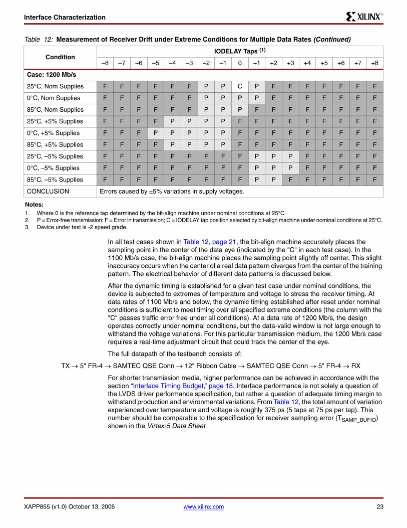
Interface Characterization
XAPP855 (v10) October 13 2006 wwwxilinxcom 24
R
Pattern Dependence of Receiver Performance
Different types of data patterns have different electrical signatures (rise and fall times jitter eye symmetry etc) A pattern with very narrow spectral content (such as a clock pattern) moves very favorably through the link because the receiver frequency response has little effect on the signal integrity However a pattern with wide spectral content (such as real data and pseudorandom patterns) stresses the links frequency response If the frequency response is not flat across the entire spectrum of the data content then the signal integrity is degraded as a result The amount of degradation measured is shown in Table 13 page 25 The DDR transmitter is looped back to the DDR receiver and different patterns are programmed to traverse the link Performance is assessed by evaluating the integrity of those patterns in the receiver
PRBS7 is a pseudorandom data pattern with a maximum run length of seven consecutive zeroes or ones PRBS15 is defined as having a maximum run length of fifteen consecutive zeroes or ones These limitations on run lengths limit the spectral content of the pattern A PRBS15 pattern has greater spectral content than a PRBS7 pattern and therefore is a more strenuous test for the link PRBS29 is the most strenuous test in Table 13 A clock pattern is effectively a PRBS1
As predicted Table 13 shows that there is more degradation for data patterns with more spectral content At 1000 Mbs and below the data eye closure is symmetrical Symmetrical eye closure is desired because it does not change the center of the eye as determined by the bit-alignment algorithm Above 1000 Mbs the eye closure becomes more asymmetrical causing the center of the data eye to diverge from the calibrated center (by only 1 tap)
In every data rate shown in Table 13 all significant pattern-dependent degradation is caused between PRBS1 (clock pat) and PRBS15 Between PRBS15 and PRBS29 there is no additional degradation recorded in any of the measurements
Interface Characterization
XAPP855 (v10) October 13 2006 wwwxilinxcom 25
R
Table 13 Link Performance for Various Types of Data Measured on a -2 Device
PatternIODELAY Taps (1)
ndash8 ndash7 ndash6 ndash5 ndash4 ndash3 ndash2 ndash1 0 +1 +2 +3 +4 +5 +6 +7 +8 +9
Case 600 Mbs
Clock Pat (0101) P P P P P P P P C P P P P P P P P P
Training Pat (0x2C) P P P P P P P P C P P P P P P P P F
PRBS7 P P P P P P P P C P P P P P P P P F
PRBS15 F P P P P P P P C P P P P P P P F F
PRBS23 F P P P P P P P C P P P P P P P F F
PRBS29 F P P P P P P P C P P P P P P P F F
Case 800 Mbs
Clock Pat (0101) F F P P P P P P C P P P P P P F F F
Training Pat (0x2C) F F P P P P P P C P P P P P P F F F
PRBS7 F F P P P P P P C P P P P P F F F F
PRBS15 F F F P P P P P C P P P P P F F F F
PRBS23 F F F P P P P P C P P P P P F F F F
PRBS29 F F F P P P P P C P P P P P F F F F
Case 1000 Mbs
Clock Pat (0101) F F F P P P P P C P P P P P F F F F
Training Pat (0x2C) F F F P P P P P C P P P P F F F F F
PRBS7 F F F F P P P P C P P P F F F F F F
PRBS15 F F F F F P P P C P P P F F F F F F
PRBS23 F F F F F P P P C P P P F F F F F F
PRBS29 F F F F F P P P C P P P F F F F F F
Case 1200 Mbs
Clock Pat (0101) F F F F P P P P C P P P P F F F F F
Training Pat (0x2C) F F F F P P P P C P P P F F F F F F
PRBS7 F F F F F P P P C P F F F F F F F F
PRBS15 F F F F F F P P C F F F F F F F F F
PRBS23 F F F F F F P P C F F F F F F F F F
PRBS29 F F F F F F P P C F F F F F F F F F
Case 1400 Mbs
Clock Pat (0101) F F F F F F P P C P P P F F F F F F
Training Pat (0x2C) F F F F F P P P C P P F F F F F F F
PRBS7 F F F F F F F P C P F F F F F F F F
PRBS15 F F F F F F F P C F F F F F F F F F
PRBS23 F F F F F F F P C F F F F F F F F F
PRBS29 F F F F F F F P C F F F F F F F F F
Notes 1 Where 0 is the reference tap determined by the bit-align machine under nominal conditions at 25degC2 P = Error-free transmission F = Error in transmission C = IODELAY tap position selected by bit-align machine under nominal conditions at 25degC
Resetting the Interface
XAPP855 (v10) October 13 2006 wwwxilinxcom 26
R
Resetting the Interface
Several dependencies determine the order in which circuits should be reset in the interface The receiver cannot begin the alignment algorithm if the transmitter is not sending the training pattern The transmitter must be reset before the receiver and time must be allowed for the training pattern to propagate across the link before the receiver comes out of reset The receiver also cannot begin the alignment algorithm until IDELAYCTRL has recovered from reset which could takes hundreds of cycles The recommended reset timing for the interface is shown in Figure 16 This reset timing is implemented in the BERT testbench for this interface
The TX reset (RST_TX) is used to reset all TX circuitry and also IDELAYCTRL The IDELAYCTRL reset is asynchronous so driving it with RST_TX is acceptable The minimum pulse width of IDELAYCTRL reset is 50 ns (TIDELAYCTRL_RPW) For that reason resets are held High for 16 clock cycles The RX reset (RST_RX) is used to reset all RX circuitry and is asserted when the IDELAYCTRL READY flag goes High indicating that the IODELAY blocks are calibrated
The timing of the READY flag in Figure 16 is a potential hazard Most likely it is High during a TX reset because it takes many cycles for IDELAYCTRL to deassert the READY flag It is easy to make the mistake of resetting the receiver too early To avoid this hazard the RX reset should be asserted only after seeing a deassertion and reassertion of the READY flag
Conclusion Based on the design and characterization described in this document the 16-Channel DDR reference design operates to the performance targets in Table 14 under all conditions of process voltage and temperature However to meet these targets over voltage and temperature the timing budget must be guaranteed according to the analysis in ldquoInterface Timing Budgetrdquo See ldquoAppendixrdquo page 27 for further justification of the maximum performance recommendations in Table 14
Figure 16 Recommended Interface Reset Timing
RST_TX
IDELAYCTRLREADY
RST_RX
16 Cycles X855_16_072406
Table 14 Performance of 16-Channel DDR Interface
Speed Grade Maximum Performance
-1 800 Mbs
-2 900 Mbs
-3 10 Gbs(1)
Notes 1 To achieve higher performance (up to 125 Gbs) see 16-channel DDR LVDS Interface with Realtime
Window Monitoring for an example of a DDR interface with real-time window monitoring
Appendix
XAPP855 (v10) October 13 2006 wwwxilinxcom 27
R
Appendix Performance Characterization Data
Refer to ldquoInterface Characterizationrdquo page 19 for explanations about how to interpret the data in the ldquoAppendixrdquo These tables show collective data eyes for the entire interface over process voltage and temperature (PVT) Three devices from each speed grade were selected for this characterization
The calibrated center position of the eye (marked by the C in the tables below) varies slightly from channel to channel (due to small skews between channels) That range is referred to as center tap range Analysis of Table 16 page 28 through Table 20 page 40 shows that the center tap range for slow and fast parts differ significantly at the same data rate (because the BIT_ALIGN_MACHINE algorithm adjusts for differences in speed)
All data in the ldquoAppendixrdquo is collected using the BERT testbench shown in Figure 2 page 2 The data pattern is PRBS23 and the devicepackage is XC5VLX50T-FF1136 The transmission path for the cases shown in Table 16 through Table 20 is repeated for convenience
TX rarr 5 FR-4 rarr SAMTEC QSE Conn rarr 12 Ribbon Cable rarr SAMTEC QSE Conn rarr 5 FR-4 rarr RX
A summary of these characterization results is shown in Table 15 Each of the nine parts were tested at 800 900 1000 1100 and 1200 Mbs When the interface is error free on all channels under all extreme conditions of temperature and voltage the particular test case is designated by a P A test case is marked FAIL when the interface suffered errors on any channel under any particular condition of voltage and temperature
Table 15 Summary of Interface Characterization Results
Device (SN) Speed Grade 800 Mbs 900 Mbs 1000Mbs 1100 Mbs 1200 Mbs
2194 -1 P P P FAIL FAIL
2219 -1 P FAIL FAIL FAIL FAIL
2199 -1 P P FAIL FAIL FAIL
001 -2 P P FAIL P FAIL
002 -2 P P P P FAIL
003 -2 P P FAIL FAIL FAIL
004 -3 P P P P P
005 -3 P P P P P
006 -3 P P P P P
Appendix
XAPP855 (v10) October 13 2006 wwwxilinxcom 28
R
Table 16 Measurement of Receiver Drift under Extreme Conditions at 800 Mbs
ConditionIODELAY Taps (1)
ndash8 ndash7 ndash6 ndash5 ndash4 ndash3 ndash2 ndash1 0 +1 +2 +3 +4 +5 +6 +7 +8
SN 2194 Speed Grade -1
25degC Nom Supplies F F F P P P P P C P P P P F F F F
0degC Nom Supplies F F F P P P P P P P P P P F F F F
85degC Nom Supplies F F F F P P P P P P P P P F F F F
25degC +5 Supplies F F P P P P P P P P P P F F F F F
0degC +5 Supplies F F P P P P P P P P P P F F F F F
85degC +5 Supplies F F P P P P P P P P P P F F F F F
25degC ndash5 Supplies F F F F F F P P P P P P P P P F F
0degC ndash5 Supplies F F F F F F P P P P P P P P P F F
85degC ndash5 Supplies F F F F F F P P P P P P P P P F F
Center Tap Range Taps 11ndash12
CONCLUSION Error free under all conditions when calibrated under nominal conditions to position C
SN 2219 Speed Grade -1
25degC Nom Supplies F F F P P P P P C P P P F F F F F
0degC Nom Supplies F F F P P P P P P P P P F F F F F
85degC Nom Supplies F F F P P P P P P P P P F F F F F
25degC +5 Supplies F P P P P P P P P P P F F F F F F
0degC +5 Supplies F P P P P P P P P P P F F F F F F
85degC +5 Supplies F P P P P P P P P P P F F F F F F
25degC ndash5 Supplies F F F F F F P P P P P P P P F F F
0degC ndash5 Supplies F F F F F F F P P P P P P P F F F
85degC ndash5 Supplies F F F F F F P P P P P P P P F F F
Center Tap Range Taps 13ndash16
CONCLUSION Error free under all conditions when calibrated under nominal conditions to position C
SN 2199 Speed Grade -1
25degC Nom Supplies F F F P P P P P C P P P P F F F F
0degC Nom Supplies F F F P P P P P P P P P P F F F F
85degC Nom Supplies F F F P P P P P P P P P P F F F F
25degC +5 Supplies F P P P P P P P P P P P F F F F F
0degC +5 Supplies F P P P P P P P P P P P F F F F F
85degC +5 Supplies F P P P P P P P P P P P F F F F F
25degC ndash5 Supplies F F F F F F P P P P P P P P P F F
0degC ndash5 Supplies F F F F F F P P P P P P P P P F F
85degC ndash5 Supplies F F F F F F P P P P P P P P P F F
Center Tap Range Taps 10ndash12
CONCLUSION Error free under all conditions when calibrated under nominal conditions to position C
Appendix
XAPP855 (v10) October 13 2006 wwwxilinxcom 29
R
SN 001 Speed Grade -2
25degC Nom Supplies F F F P P P P P C P P P P F F F F
0degC Nom Supplies F F F P P P P P P P P P P F F F F
85degC Nom Supplies F F F P P P P P P P P P P F F F F
25degC +5 Supplies F P P P P P P P P P P P F F F F F
0degC +5 Supplies F P P P P P P P P P P F F F F F F
85degC +5 Supplies F P P P P P P P P P P P F F F F F
25degC ndash5 Supplies F F F F F P P P P P P P P P P F F
0degC ndash5 Supplies F F F F F P P P P P P P P P P F F
85degC ndash5 Supplies F F F F F P P P P P P P P P P F F
Center Tap Range Taps 10ndash12
CONCLUSION Error free under all conditions when calibrated under nominal conditions to position C
SN 002 Speed Grade -2
25degC Nom Supplies F F F P P P P P C P P P P F F F F
0degC Nom Supplies F F F P P P P P P P P P P F F F F
85degC Nom Supplies F F F P P P P P P P P P P F F F F
25degC +5 Supplies F P P P P P P P P P P P F F F F F
0degC +5 Supplies F P P P P P P P P P P P F F F F F
85degC +5 Supplies F F P P P P P P P P P P F F F F F
25degC ndash5 Supplies F F F F F P P P P P P P P P P F F
0degC ndash5 Supplies F F F F F P P P P P P P P P P F F
85degC ndash5 Supplies F F F F F P P P P P P P P P P F F
Center Tap Range Taps 10ndash12
CONCLUSION Error free under all conditions when calibrated under nominal conditions to position C
SN 003 Speed Grade -2
25degC Nom Supplies F F F P P P P P C P P P P F F F F
0degC Nom Supplies F F F P P P P P P P P P P F F F F
85degC Nom Supplies F F F P P P P P P P P P P F F F F
25degC +5 Supplies F P P P P P P P P P P P F F F F F
0degC +5 Supplies F P P P P P P P P P P F F F F F F
85degC +5 Supplies F P P P P P P P P P P P F F F F F
25degC ndash5 Supplies F F F F F F P P P P P P P P P F F
0degC ndash5 Supplies F F F F F F P P P P P P P P P F F
85degC ndash5 Supplies F F F F F F P P P P P P P P P F F
Center Tap Range Taps 11ndash13
CONCLUSION Error free under all conditions when calibrated under nominal conditions to position C
Table 16 Measurement of Receiver Drift under Extreme Conditions at 800 Mbs (Continued)
ConditionIODELAY Taps (1)
ndash8 ndash7 ndash6 ndash5 ndash4 ndash3 ndash2 ndash1 0 +1 +2 +3 +4 +5 +6 +7 +8
Appendix
XAPP855 (v10) October 13 2006 wwwxilinxcom 30
R
SN 004 Speed Grade -3
25degC Nom Supplies F F F P P P P P C P P P P F F F F
0degC Nom Supplies F F F P P P P P P P P P F F F F F
85degC Nom Supplies F F F P P P P P P P P P P F F F F
25degC +5 Supplies F P P P P P P P P P P P F F F F F
0degC +5 Supplies F P P P P P P P P P P P F F F F F
85degC +5 Supplies F F P P P P P P P P P P F F F F F
25degC ndash5 Supplies F F F F F P P P P P P P P P F F F
0degC ndash5 Supplies F F F F F P P P P P P P P P F F F
85degC ndash5 Supplies F F F F F P P P P P P P P P F F F
Center Tap Range Taps 8ndash9 23ndash24
CONCLUSION Error free under all conditions when calibrated under nominal conditions to position C
SN 005 Speed Grade -3
25degC Nom Supplies F F P P P P P P C P P P P F F F F
0degC Nom Supplies F F P P P P P P P P P P P F F F F
85degC Nom Supplies F F F P P P P P P P P P P P F F F
25degC +5 Supplies F P P P P P P P P P P P F F F F F
0degC +5 Supplies F P P P P P P P P P P P F F F F F
85degC +5 Supplies F P P P P P P P P P P P F F F F F
25degC ndash5 Supplies F F F F P P P P P P P P P P P F F
0degC ndash5 Supplies F F F F P P P P P P P P P P P F F
85degC ndash5 Supplies F F F F P P P P P P P P P P P F F
Center Tap Range Taps 9ndash10
CONCLUSION Error free under all conditions when calibrated under nominal conditions to position C
SN 006 Speed Grade -3
25degC Nom Supplies F F P P P P P P C P P P P F F F F
0degC Nom Supplies F F P P P P P P P P P P P F F F F
85degC Nom Supplies F F F P P P P P P P P P P F F F F
25degC +5 Supplies F P P P P P P P P P P P F F F F F
0degC +5 Supplies F P P P P P P P P P P P F F F F F
85degC +5 Supplies F F P P P P P P P P P P F F F F F
25degC ndash5 Supplies F F F P P P P P P P P P P P F F F
0degC ndash5 Supplies F F F P P P P P P P P P P P F F F
85degC ndash5 Supplies F F F F F P P P P P P P P P F F F
Center Tap Range Taps 8ndash9 23ndash24
CONCLUSION Error free under all conditions when calibrated under nominal conditions to position C
Notes 1 IODELAY taps where 0 is the reference tap determined by the bit align machine at nominal voltage and 25degC2 P = Error-free transmission F = Error in transmission C = IODELAY tap position selected by bit-align machine under nominal conditions at 25degC
Table 16 Measurement of Receiver Drift under Extreme Conditions at 800 Mbs (Continued)
ConditionIODELAY Taps (1)
ndash8 ndash7 ndash6 ndash5 ndash4 ndash3 ndash2 ndash1 0 +1 +2 +3 +4 +5 +6 +7 +8
Appendix
XAPP855 (v10) October 13 2006 wwwxilinxcom 31
R
Table 17 Measurement of Receiver Drift under Extreme Conditions at 900 Mbs
ConditionIODELAY Taps (1)
ndash8 ndash7 ndash6 ndash5 ndash4 ndash3 ndash2 ndash1 0 +1 +2 +3 +4 +5 +6 +7 +8
SN 2194 Speed Grade -1
25degC Nom Supplies F F F F F P P P C P P P F F F F F
0degC Nom Supplies F F F F F P P P P P P P F F F F F
85degC Nom Supplies F F F F F P P P P P P P P F F F F
25degC +5 Supplies F F F P P P P P P P P F F F F F F
0degC +5 Supplies F F F P P P P P P P P F F F F F F
85degC +5 Supplies F F F P P P P P P P P F F F F F F
25degC ndash5 Supplies F F F F F F F P P P P P P P F F F
0degC ndash5 Supplies F F F F F F F P P P P P P P F F F
85degC ndash5 Supplies F F F F F F F P P P P P P P F F F
Center Tap Range Taps 11ndash12
CONCLUSION Error free under all conditions when calibrated under nominal conditions to position C
SN 2219 Speed Grade -1
25degC Nom Supplies F F F F F P P P C P P P F F F F F
0degC Nom Supplies F F F F F P P P P P P P F F F F F
85degC Nom Supplies F F F F F P P P P P P P F F F F F
25degC +5 Supplies F F F P P P P P P P F F F F F F F
0degC +5 Supplies F F F P P P P P P P F F F F F F F
85degC +5 Supplies F F F P P P P P P P F F F F F F F
25degC ndash5 Supplies F F F F F F F F F P P P P P F F F
0degC ndash5 Supplies F F F F F F F F F P P P P P F F F
85degC ndash5 Supplies F F F F F F F F P P P P P P F F F
Center Tap Range Taps 12ndash15
CONCLUSION Errors caused by ndash5 variation in supply voltage
SN 2199 Speed Grade -1
25degC Nom Supplies F F F F F P P P C P P P F F F F F
0degC Nom Supplies F F F F F P P P P P P P F F F F F
85degC Nom Supplies F F F F F P P P P P P P F F F F F
25degC +5 Supplies F F F P P P P P P P P F F F F F F
0degC +5 Supplies F F F P P P P P P P P F F F F F F
85degC +5 Supplies F F F P P P P P P P P F F F F F F
25degC ndash5 Supplies F F F F F F F F P P P P P P F F F
0degC ndash5 Supplies F F F F F F F F P P P P P P F F F
85degC ndash5 Supplies F F F F F F F F P P P P P P F F F
Center Tap Range Taps 10ndash12
CONCLUSION Error free under all conditions when calibrated under nominal conditions to position C
Appendix
XAPP855 (v10) October 13 2006 wwwxilinxcom 32
R
SN 001 Speed Grade -2
25degC Nom Supplies F F F F P P P P C P P P P F F F F
0degC Nom Supplies F F F F P P P P P P P P P F F F F
85degC Nom Supplies F F F F F P P P P P P P P F F F F
25degC +5 Supplies F F P P P P P P P P P F F F F F F
0degC +5 Supplies F F P P P P P P P P P F F F F F F
85degC +5 Supplies F F F P P P P P P P P P F F F F F
25degC ndash5 Supplies F F F F F F F P P P P P P P F F F
0degC ndash5 Supplies F F F F F F F P P P P P P P F F F
85degC ndash5 Supplies F F F F F F F P P P P P P P F F F
Center Tap Range Taps 9ndash11
CONCLUSION Error free under all conditions when calibrated under nominal conditions to position C
SN 002 Speed Grade -2
25degC Nom Supplies F F F F P P P P C P P P P F F F F
0degC Nom Supplies F F F F P P P P P P P P F F F F F
85degC Nom Supplies F F F F F P P P P P P P P F F F F
25degC +5 Supplies F F F P P P P P P P P F F F F F F
0degC +5 Supplies F F F P P P P P P P P F F F F F F
85degC +5 Supplies F F F P P P P P P P P P F F F F F
25degC ndash5 Supplies F F F F F F F P P P P P P P F F F
0degC ndash5 Supplies F F F F F F F P P P P P P P F F F
85degC ndash5 Supplies F F F F F F F P P P P P P P F F F
Center Tap Range Taps 10ndash12
CONCLUSION Error free under all conditions when calibrated under nominal conditions to position C
SN 003 Speed Grade -2
25degC Nom Supplies F F F F F P P P C P P P P F F F F
0degC Nom Supplies F F F F F P P P P P P P P F F F F
85degC Nom Supplies F F F F F P P P P P P P P F F F F
25degC +5 Supplies F F P P P P P P P P P F F F F F F
0degC +5 Supplies F F P P P P P P P P P F F F F F F
85degC +5 Supplies F F F P P P P P P P P F F F F F F
25degC ndash5 Supplies F F F F F F F P P P P P P P F F F
0degC ndash5 Supplies F F F F F F F F P P P P P P F F F
85degC ndash5 Supplies F F F F F F F P P P P P P P F F F
Center Tap Range Taps 11ndash13
CONCLUSION Error free under all conditions when calibrated under nominal conditions to position C
Table 17 Measurement of Receiver Drift under Extreme Conditions at 900 Mbs (Continued)
ConditionIODELAY Taps (1)
ndash8 ndash7 ndash6 ndash5 ndash4 ndash3 ndash2 ndash1 0 +1 +2 +3 +4 +5 +6 +7 +8
Appendix
XAPP855 (v10) October 13 2006 wwwxilinxcom 33
R
SN 004 Speed Grade -3
25degC Nom Supplies F F F F P P P P C P P P P F F F F
0degC Nom Supplies F F F P P P P P P P P P P F F F F
85degC Nom Supplies F F F F P P P P P P P P P F F F F
25degC +5 Supplies F F F P P P P P P P P P F F F F F
0degC +5 Supplies F F F P P P P P P P P P F F F F F
85degC +5 Supplies F F F P P P P P P P P P F F F F F
25degC ndash5 Supplies F F F F F F P P P P P P P P F F F
0degC ndash5 Supplies F F F F F F P P P P P P P P F F F
85degC ndash5 Supplies F F F F F F P P P P P P P P F F F
Center Tap Range Taps 7ndash8
CONCLUSION Error free under all conditions when calibrated under nominal conditions to position C
SN 005 Speed Grade ndash3
25degC Nom Supplies F F F P P P P P C P P P P F F F F
0degC Nom Supplies F F F P P P P P P P P P P F F F F
85degC Nom Supplies F F F F P P P P P P P P P F F F F
25degC +5 Supplies F F P P P P P P P P P P F F F F F
0degC +5 Supplies F F P P P P P P P P P P F F F F F
85degC +5 Supplies F F F P P P P P P P P P F F F F F
25degC ndash5 Supplies F F F F F F P P P P P P P P F F F
0degC ndash5 Supplies F F F F F P P P P P P P P P F F F
85degC ndash5 Supplies F F F F F F P P P P P P P P F F F
Center Tap Range Taps 9ndash10
CONCLUSION Error free under all conditions when calibrated under nominal conditions to position C
SN 006 Speed Grade -3
25degC Nom Supplies F F F F P P P P C P P P P F F F F
0degC Nom Supplies F F F F P P P P P P P P P F F F F
85degC Nom Supplies F F F F P P P P P P P P P F F F F
25degC +5 Supplies F F P P P P P P P P P P F F F F F
0degC +5 Supplies F F P P P P P P P P P P F F F F F
85degC +5 Supplies F F F P P P P P P P P P F F F F F
25degC ndash5 Supplies F F F F F P P P P P P P P P F F F
0degC ndash5 Supplies F F F F F P P P P P P P P P F F F
85degC ndash5 Supplies F F F F F F P P P P P P P P F F F
Center Tap Range Taps 7ndash8
CONCLUSION Error free under all conditions when calibrated under nominal conditions to position C
Notes 1 IODELAY taps where 0 is the reference tap determined by the bit align machine at nominal voltage and 25degC2 P = Error-free transmission F = Error in transmission C = IODELAY tap position selected by bit-align machine under nominal conditions at 25degC
Table 17 Measurement of Receiver Drift under Extreme Conditions at 900 Mbs (Continued)
ConditionIODELAY Taps (1)
ndash8 ndash7 ndash6 ndash5 ndash4 ndash3 ndash2 ndash1 0 +1 +2 +3 +4 +5 +6 +7 +8
Appendix
XAPP855 (v10) October 13 2006 wwwxilinxcom 34
R
Table 18 Measurement of Receiver Drift under Extreme Conditions at 1000 Mbs
ConditionIODELAY Taps (1)
ndash8 ndash7 ndash6 ndash5 ndash4 ndash3 ndash2 ndash1 0 +1 +2 +3 +4 +5 +6 +7 +8
SN 2194 Speed Grade -1
25degC Nom Supplies F F F F F P P P C P P F F F F F F
0degC Nom Supplies F F F F F P P P P P P F F F F F F
85degC Nom Supplies F F F F F P P P P P P F F F F F F
25degC +5 Supplies F F F P P P P P P P F F F F F F F
0degC +5 Supplies F F F P P P P P P P F F F F F F F
85degC +5 Supplies F F F F P P P P P P F F F F F F F
25degC ndash5 Supplies F F F F F F F F P P P P P F F F F
0degC ndash5 Supplies F F F F F F F F P P P P P F F F F
85degC ndash5 Supplies F F F F F F F F P P P P P F F F F
Center Tap Range Taps 12ndash13
CONCLUSION Error free under all conditions when calibrated under nominal conditions to position C
SN 2219 Speed Grade -1
25degC Nom Supplies F F F F F F P P C P P F F F F F F
0degC Nom Supplies F F F F F F P P P P P F F F F F F
85degC Nom Supplies F F F F F F P P P P P F F F F F F
25degC +5 Supplies F F F P P P P P P F F F F F F F F
0degC +5 Supplies F F F P P P P P P F F F F F F F F
85degC +5 Supplies F F F F P P P P P F F F F F F F F
25degC ndash5 Supplies F F F F F F F F F P P P P F F F F
0degC ndash5 Supplies F F F F F F F F F F P P P F F F F
85degC ndash5 Supplies F F F F F F F F F P P P P F F F F
Center Tap Range Taps 14ndash17
CONCLUSION Errors caused by ndash5 variation in supply voltage
SN 2199 Speed Grade -1
25degC Nom Supplies F F F F F F P P C P P F F F F F F
0degC Nom Supplies F F F F F F P P P P P F F F F F F
85degC Nom Supplies F F F F F F P P P P P F F F F F F
25degC +5 Supplies F F F F P P P P P P F F F F F F F
0degC +5 Supplies F F F F P P P P P P F F F F F F F
85degC +5 Supplies F F F F P P P P P P F F F F F F F
25degC ndash5 Supplies F F F F F F F F F P P P P F F F F
0degC ndash5 Supplies F F F F F F F F F P P P P F F F F
85degC ndash5 Supplies F F F F F F F F F P P P P F F F F
Center Tap Range Taps 12ndash14
CONCLUSION Errors caused by ndash5 variation in supply voltage
Appendix
XAPP855 (v10) October 13 2006 wwwxilinxcom 35
R
SN 001 Speed Grade -2
25degC Nom Supplies F F F F F F P P C P P P F F F F F
0degC Nom Supplies F F F F F F P P P P P P F F F F F
85degC Nom Supplies F F F F F F P P P P P P F F F F F
25degC +5 Supplies F F F F P P P P P P F F F F F F F
0degC +5 Supplies F F F F P P P P P P F F F F F F F
85degC +5 Supplies F F F F P P P P P P P F F F F F F
25degC ndash5 Supplies F F F F F F F F F P P P P F F F F
0degC ndash5 Supplies F F F F F F F F F P P P P F F F F
85degC ndash5 Supplies F F F F F F F F F P P P P F F F F
Center Tap Range Taps 11ndash12
CONCLUSION Errors caused by ndash5 variation in supply voltage
SN 002 Speed Grade -2
25degC Nom Supplies F F F F F P P P C P P F F F F F F
0degC Nom Supplies F F F F F P P P P P P P F F F F F
85degC Nom Supplies F F F F F P P P P P P P F F F F F
25degC +5 Supplies F F F F P P P P P P F F F F F F F
0degC +5 Supplies F F F P P P P P P P F F F F F F F
85degC +5 Supplies F F F F P P P P P P P F F F F F F
25degC ndash5 Supplies F F F F F F F P P P P P P F F F F
0degC ndash5 Supplies F F F F F F F P P P P P P F F F F
85degC ndash5 Supplies F F F F F F F P P P P P P F F F F
Center Tap Range Taps 11ndash13
CONCLUSION Error free under all conditions when calibrated under nominal conditions to position C
SN 003 Speed Grade -2
25degC Nom Supplies F F F F F F P P C P P F F F F F F
0degC Nom Supplies F F F F F F P P P P P F F F F F F
85degC Nom Supplies F F F F F F P P P P P F F F F F F
25degC +5 Supplies F F F F P P P P P P F F F F F F F
0degC +5 Supplies F F F F P P P P P P F F F F F F F
85degC +5 Supplies F F F F P P P P P P F F F F F F F
25degC ndash5 Supplies F F F F F F F F F P P P P F F F F
0degC ndash5 Supplies F F F F F F F F F P P P P F F F F
85degC ndash5 Supplies F F F F F F F F F P P P P F F F F
Center Tap Range Taps 13ndash14
CONCLUSION Errors caused by ndash5 variation in supply voltage
Table 18 Measurement of Receiver Drift under Extreme Conditions at 1000 Mbs (Continued)
ConditionIODELAY Taps (1)
ndash8 ndash7 ndash6 ndash5 ndash4 ndash3 ndash2 ndash1 0 +1 +2 +3 +4 +5 +6 +7 +8
Appendix
XAPP855 (v10) October 13 2006 wwwxilinxcom 36
R
SN 004 Speed Grade -3
25degC Nom Supplies F F F F F P P P C P P P F F F F F
0degC Nom Supplies F F F F F P P P P P P P F F F F F
85degC Nom Supplies F F F F F P P P P P P P F F F F F
25degC +5 Supplies F F F P P P P P P P P F F F F F F
0degC +5 Supplies F F F P P P P P P P P F F F F F F
85degC +5 Supplies F F F F P P P P P P P P F F F F F
25degC ndash5 Supplies F F F F F F F P P P P P P F F F F
0degC ndash5 Supplies F F F F F F F P P P P P P F F F F
85degC ndash5 Supplies F F F F F F F P P P P P P P F F F
Center Tap Range Taps 9ndash10
CONCLUSION Error free under all conditions when calibrated under nominal conditions to position C
SN 005 Speed Grade -3
25degC Nom Supplies F F F F P P P P C P P P F F F F F
0degC Nom Supplies F F F F P P P P P P P P F F F F F
85degC Nom Supplies F F F F P P P P P P P P F F F F F
25degC +5 Supplies F F F P P P P P P P P F F F F F F
0degC +5 Supplies F F P P P P P P P P P F F F F F F
85degC +5 Supplies F F F P P P P P P P P F F F F F F
25degC ndash5 Supplies F F F F F F P P P P P P P P F F F
0degC ndash5 Supplies F F F F F F P P P P P P P P F F F
85degC ndash5 Supplies F F F F F F P P P P P P P F F F F
Center Tap Range Taps 11ndash12
CONCLUSION Error free under all conditions when calibrated under nominal conditions to position C
SN 006 Speed Grade -3
25degC Nom Supplies F F F F P P P P C P P P F F F F F
0degC Nom Supplies F F F F P P P P P P P P F F F F F
85degC Nom Supplies F F F F P P P P P P P P F F F F F
25degC +5 Supplies F F F P P P P P P P P F F F F F F
0degC +5 Supplies F F F P P P P P P P P F F F F F F
85degC +5 Supplies F F F P P P P P P P P F F F F F F
25degC ndash5 Supplies F F F F F F P P P P P P P F F F F
0degC ndash5 Supplies F F F F F F P P P P P P P F F F F
85degC ndash5 Supplies F F F F F F P P P P P P P F F F F
Center Tap Range Taps 9ndash10
CONCLUSION Error free under all conditions when calibrated under nominal conditions to position C
Notes 1 IODELAY taps where 0 is the reference tap determined by the bit align machine at nominal voltage and 25degC2 P = Error-free transmission F = Error in transmission C = IODELAY tap position selected by bit-align machine under nominal conditions at 25degC
Table 18 Measurement of Receiver Drift under Extreme Conditions at 1000 Mbs (Continued)
ConditionIODELAY Taps (1)
ndash8 ndash7 ndash6 ndash5 ndash4 ndash3 ndash2 ndash1 0 +1 +2 +3 +4 +5 +6 +7 +8
Appendix
XAPP855 (v10) October 13 2006 wwwxilinxcom 37
R
Table 19 Measurement of Receiver Drift under Extreme Conditions at 1100 Mbs
ConditionIODELAY Taps (1)
ndash8 ndash7 ndash6 ndash5 ndash4 ndash3 ndash2 ndash1 0 +1 +2 +3 +4 +5 +6 +7 +8
SN 2194 Speed Grade -1
25degC Nom Supplies F F F F F F P P C P P F F F F F F
0degC Nom Supplies F F F F F F P P P P P F F F F F F
85degC Nom Supplies F F F F F F P P P P P F F F F F F
25degC +5 Supplies F F F F P P P P P F F F F F F F F
0degC +5 Supplies F F F F P P P P P F F F F F F F F
85degC +5 Supplies F F F F P P P P P F F F F F F F F
25degC ndash5 Supplies F F F F F F F F F P P P F F F F F
0degC ndash5 Supplies F F F F F F F F F P P P F F F F F
85degC ndash5 Supplies F F F F F F F F F P P P F F F F F
Center Tap Range Taps 13ndash14
CONCLUSION Errors caused by ndash5 variation in supply voltage
SN 2219 Speed Grade -1
25degC Nom Supplies F F F F F F P P C P F F F F F F F
0degC Nom Supplies F F F F F F P P P P F F F F F F F
85degC Nom Supplies F F F F F F P P P P F F F F F F F
25degC +5 Supplies F F F F P P P P F F F F F F F F F
0degC +5 Supplies F F F F P P P P F F F F F F F F F
85degC +5 Supplies F F F F P P P P F F F F F F F F F
25degC ndash5 Supplies F F F F F F F F F F P P F F F F F
0degC ndash5 Supplies F F F F F F F F F F P P F F F F F
85degC ndash5 Supplies F F F F F F F F F P P P F F F F F
Center Tap Range Taps 6 15ndash17
CONCLUSION Errors caused by plusmn5 variation in supply voltage
SN 2199 Speed Grade -1
25degC Nom Supplies F F F F F F F P C P F F F F F F F
0degC Nom Supplies F F F F F F F P P P F F F F F F F
85degC Nom Supplies F F F F F F F P P P F F F F F F F
25degC +5 Supplies F F F F P P P P P F F F F F F F F
0degC +5 Supplies F F F F P P P P P F F F F F F F F
85degC +5 Supplies F F F F F P P P P F F F F F F F F
25degC ndash5 Supplies F F F F F F F F F F P P F F F F F
0degC ndash5 Supplies F F F F F F F F F F P P F F F F F
85degC ndash5 Supplies F F F F F F F F F F P P F F F F F
Center Tap Range Taps 13ndash15
CONCLUSION Errors caused by ndash5 variation in supply voltage
Appendix
XAPP855 (v10) October 13 2006 wwwxilinxcom 38
R
SN 001 Speed Grade -2
25degC Nom Supplies F F F F F F P P C P P F F F F F F
0degC Nom Supplies F F F F F F P P P P P F F F F F F
85degC Nom Supplies F F F F F F P P P P P F F F F F F
25degC +5 Supplies F F F F P P P P P F F F F F F F F
0degC +5 Supplies F F F F P P P P P F F F F F F F F
85degC +5 Supplies F F F F P P P P P F F F F F F F F
25degC ndash5 Supplies F F F F F F F F P P P P F F F F F
0degC ndash5 Supplies F F F F F F F F P P P P F F F F F
85degC ndash5 Supplies F F F F F F F F P P P P F F F F F
Center Tap Range Taps 12ndash13
CONCLUSION Error free under all conditions when calibrated under nominal conditions to position C
SN 002 Speed Grade -2
25degC Nom Supplies F F F F F P P P C P F F F F F F F
0degC Nom Supplies F F F F F P P P P P F F F F F F F
85degC Nom Supplies F F F F F F P P P P F F F F F F F
25degC +5 Supplies F F F F P P P P P F F F F F F F F
0degC +5 Supplies F F F P P P P P P F F F F F F F F
85degC +5 Supplies F F F F P P P P P F F F F F F F F
25degC ndash5 Supplies F F F F F F F F P P P P F F F F F
0degC ndash5 Supplies F F F F F F F F P P P P F F F F F
85degC ndash5 Supplies F F F F F F F F P P P P F F F F F
Center Tap Range Taps 13ndash14
CONCLUSION Error free under all conditions when calibrated under nominal conditions to position C
SN 003 Speed Grade -2
25degC Nom Supplies F F F F F F F P C P F F F F F F F
0degC Nom Supplies F F F F F F F P P P F F F F F F F
85degC Nom Supplies F F F F F F F P P P P F F F F F F
25degC +5 Supplies F F F F F P P P P F F F F F F F F
0degC +5 Supplies F F F F F P P P P F F F F F F F F
85degC +5 Supplies F F F F F P P P P F F F F F F F F
25degC ndash5 Supplies F F F F F F F F F F P P F F F F F
0degC ndash5 Supplies F F F F F F F F F F P P F F F F F
85degC ndash5 Supplies F F F F F F F F F P P P F F F F F
Center Tap Range Taps 14ndash16
CONCLUSION Errors caused by ndash5 variation in supply voltage
Table 19 Measurement of Receiver Drift under Extreme Conditions at 1100 Mbs (Continued)
ConditionIODELAY Taps (1)
ndash8 ndash7 ndash6 ndash5 ndash4 ndash3 ndash2 ndash1 0 +1 +2 +3 +4 +5 +6 +7 +8
Appendix
XAPP855 (v10) October 13 2006 wwwxilinxcom 39
R
SN 004 Speed Grade -3
25degC Nom Supplies F F F F F P P P C P P F F F F F F
0degC Nom Supplies F F F F F P P P P P P F F F F F F
85degC Nom Supplies F F F F F F P P P P P F F F F F F
25degC +5 Supplies F F F F P P P P P P F F F F F F F
0degC +5 Supplies F F F F P P P P P P F F F F F F F
85degC +5 Supplies F F F F P P P P P P F F F F F F F
25degC ndash5 Supplies F F F F F F F F P P P P F F F F F
0degC ndash5 Supplies F F F F F F F P P P P P F F F F F
85degC ndash5 Supplies F F F F F F F F P P P P P F F F F
Center Tap Range Taps 9ndash10
CONCLUSION Error free under all conditions when calibrated under nominal conditions to position C
SN 005 Speed Grade -3
25degC Nom Supplies F F F F F P P P C P P F F F F F F
0degC Nom Supplies F F F F F P P P P P P F F F F F F
85degC Nom Supplies F F F F F F P P P P P F F F F F F
25degC +5 Supplies F F F F P P P P P P F F F F F F F
0degC +5 Supplies F F F F P P P P P P F F F F F F F
85degC +5 Supplies F F F F P P P P P P F F F F F F F
25degC ndash5 Supplies F F F F F F F P P P P P P F F F F
0degC ndash5 Supplies F F F F F F F P P P P P P F F F F
85degC ndash5 Supplies F F F F F F F P P P P P P F F F F
Center Tap Range Taps 11ndash12
CONCLUSION Error free under all conditions when calibrated under nominal conditions to position C
SN 006 Speed Grade -3
25degC Nom Supplies F F F F F P P P C P P P F F F F F
0degC Nom Supplies F F F F F P P P P P P F F F F F F
85degC Nom Supplies F F F F F P P P P P P P F F F F F
25degC +5 Supplies F F F F P P P P P P P F F F F F F
0degC +5 Supplies F F F P P P P P P P F F F F F F F
85degC +5 Supplies F F F F P P P P P P P F F F F F F
25degC ndash5 Supplies F F F F F F P P P P P P P F F F F
0degC ndash5 Supplies F F F F F F P P P P P P P F F F F
85degC ndash5 Supplies F F F F F F F P P P P P P F F F F
Center Tap Range Taps 9ndash10
CONCLUSION Error free under all conditions when calibrated under nominal conditions to position C
Notes 1 IODELAY taps where 0 is the reference tap determined by the bit align machine at nominal voltage and 25degC2 P = Error-free transmission F = Error in transmission C = IODELAY tap position selected by bit-align machine under nominal conditions at 25degC
Table 19 Measurement of Receiver Drift under Extreme Conditions at 1100 Mbs (Continued)
ConditionIODELAY Taps (1)
ndash8 ndash7 ndash6 ndash5 ndash4 ndash3 ndash2 ndash1 0 +1 +2 +3 +4 +5 +6 +7 +8
Appendix
XAPP855 (v10) October 13 2006 wwwxilinxcom 40
R
Table 20 Measurement of Receiver Drift under Extreme Conditions at 1200 Mbs
ConditionIODELAY Taps (1)
ndash8 ndash7 ndash6 ndash5 ndash4 ndash3 ndash2 ndash1 0 +1 +2 +3 +4 +5 +6 +7 +8
SN 2194 Speed Grade -1
25degC Nom Supplies F F F F F F F P C F F F F F F F F
0degC Nom Supplies F F F F F F F P P F F F F F F F F
85degC Nom Supplies F F F F F F F P P F F F F F F F F
25degC +5 Supplies F F F F P P P P F F F F F F F F F
0degC +5 Supplies F F F F P P P P F F F F F F F F F
85degC +5 Supplies F F F F F P P P F F F F F F F F F
25degC ndash5 Supplies F F F F F F F F F P P F F F F F F
0degC ndash5 Supplies F F F F F F F F F F P F F F F F F
85degC ndash5 Supplies F F F F F F F F F P F F F F F F F
Center Tap Range Taps 13ndash15
CONCLUSION Errors caused by plusmn5 variation in supply voltage
SN 2219 Speed Grade -1
25degC Nom Supplies F F F F F F F F C F F F F F F F F
0degC Nom Supplies F F F F F F F P P F F F F F F F F
85degC Nom Supplies F F F F F F F F P F F F F F F F F
25degC +5 Supplies F F F F F P P P F F F F F F F F F
0degC +5 Supplies F F F F F P P P F F F F F F F F F
85degC +5 Supplies F F F F F F P P F F F F F F F F F
25degC ndash5 Supplies F F F F F F F F F F F F F F F F F
0degC ndash5 Supplies F F F F F F F F F F F F F F F F F
85degC ndash5 Supplies F F F F F F F F F F F F F F F F F
Center Tap Range Taps 6ndash7 16ndash17
CONCLUSION Errors caused by plusmn5 variation in supply voltage
SN 2199 Speed Grade -1
25degC Nom Supplies F F F F F F F P C F F F F F F F F
0degC Nom Supplies F F F F F F F P P F F F F F F F F
85degC Nom Supplies F F F F F F F F P F F F F F F F F
25degC +5 Supplies F F F F F P P P F F F F F F F F F
0degC +5 Supplies F F F F F P P P F F F F F F F F F
85degC +5 Supplies F F F F F P P P F F F F F F F F F
25degC ndash5 Supplies F F F F F F F F F F F F F F F F F
0degC ndash5 Supplies F F F F F F F F F F F F F F F F F
85degC ndash5 Supplies F F F F F F F F F F F F F F F F F
Center Tap Range Taps 13ndash15
CONCLUSION Errors caused by plusmn5 variation in supply voltage
Appendix
XAPP855 (v10) October 13 2006 wwwxilinxcom 41
R
SN 001 Speed Grade -2
25degC Nom Supplies F F F F F F F P C P F F F F F F F
0degC Nom Supplies F F F F F F F P P P F F F F F F F
85degC Nom Supplies F F F F F F F P P P F F F F F F F
25degC +5 Supplies F F F F F P P P P F F F F F F F F
0degC +5 Supplies F F F F P P P P P F F F F F F F F
85degC +5 Supplies F F F F F P P P P F F F F F F F F
25degC ndash5 Supplies F F F F F F F F F F P F F F F F F
0degC ndash5 Supplies F F F F F F F F F F P F F F F F F
85degC ndash5 Supplies F F F F F F F F F F P F F F F F F
Center Tap Range Taps 12ndash13
CONCLUSION Errors caused by ndash5 variation in supply voltage
SN 002 Speed Grade -2
25degC Nom Supplies F F F F F F P P C P F F F F F F F
0degC Nom Supplies F F F F F F P P P P F F F F F F F
85degC Nom Supplies F F F F F F F P P P F F F F F F F
25degC +5 Supplies F F F F P P P P F F F F F F F F F
0degC +5 Supplies F F F F P P P P F F F F F F F F F
85degC +5 Supplies F F F F F P P P F F F F F F F F F
25degC ndash5 Supplies F F F F F F F F P P P F F F F F F
0degC ndash5 Supplies F F F F F F F F P P P F F F F F F
85degC ndash5 Supplies F F F F F F F F F P P F F F F F F
Center Tap Range Taps 13ndash14
CONCLUSION Errors caused by plusmn5 variation in supply voltage
SN 003 Speed Grade -2
25degC Nom Supplies F F F F F F F P C F F F F F F F F
0degC Nom Supplies F F F F F F F P P F F F F F F F F
85degC Nom Supplies F F F F F F F F P F F F F F F F F
25degC +5 Supplies F F F F F P P P F F F F F F F F F
0degC +5 Supplies F F F F F P P P F F F F F F F F F
85degC +5 Supplies F F F F F F P P F F F F F F F F F
25degC ndash5 Supplies F F F F F F F F F F F F F F F F F
0degC ndash5 Supplies F F F F F F F F F F F F F F F F F
85degC ndash5 Supplies F F F F F F F F F F F F F F F F F
Center Tap Range Taps 14ndash15
CONCLUSION Errors caused by plusmn5 variation in supply voltage
Table 20 Measurement of Receiver Drift under Extreme Conditions at 1200 Mbs (Continued)
ConditionIODELAY Taps (1)
ndash8 ndash7 ndash6 ndash5 ndash4 ndash3 ndash2 ndash1 0 +1 +2 +3 +4 +5 +6 +7 +8
Appendix
XAPP855 (v10) October 13 2006 wwwxilinxcom 42
R
SN 004 Speed Grade -3
25degC Nom Supplies F F F F F F P P C P F F F F F F F
0degC Nom Supplies F F F F F P P P P P F F F F F F F
85degC Nom Supplies F F F F F F P P P P F F F F F F F
25degC +5 Supplies F F F F P P P P P F F F F F F F F
0degC +5 Supplies F F F F P P P P P F F F F F F F F
85degC +5 Supplies F F F F F P P P P F F F F F F F F
25degC ndash5 Supplies F F F F F F F F P P P F F F F F F
0degC ndash5 Supplies F F F F F F F F P P P F F F F F F
85degC ndash5 Supplies F F F F F F F F P P P F F F F F F
Center Tap Range Taps 9ndash11
CONCLUSION Error free under all conditions when calibrated under nominal conditions to position C
SN 005 Speed Grade -3
25degC Nom Supplies F F F F F P P P C P F F F F F F F
0degC Nom Supplies F F F F F P P P P P F F F F F F F
85degC Nom Supplies F F F F F F P P P P F F F F F F F
25degC +5 Supplies F F F F P P P P P F F F F F F F F
0degC +5 Supplies F F F P P P P P P F F F F F F F F
85degC +5 Supplies F F F F P P P P P F F F F F F F F
25degC ndash5 Supplies F F F F F F F P P P P P F F F F F
0degC ndash5 Supplies F F F F F F F P P P P P F F F F F
85degC ndash5 Supplies F F F F F F F F P P P F F F F F F
Center Tap Range Taps 11ndash13
CONCLUSION Error free under all conditions when calibrated under nominal conditions to position C
SN 006 Speed Grade -3
25degC Nom Supplies F F F F F P P P C P F F F F F F F
0degC Nom Supplies F F F F F P P P P P F F F F F F F
85degC Nom Supplies F F F F F P P P P P F F F F F F F
25degC +5 Supplies F F F P P P P P P F F F F F F F F
0degC +5 Supplies F F F P P P P P P F F F F F F F F
85degC +5 Supplies F F F F P P P P P F F F F F F F F
25degC ndash5 Supplies F F F F F F F P P P P F F F F F F
0degC ndash5 Supplies F F F F F F P P P P P F F F F F F
85degC ndash5 Supplies F F F F F F F P P P P F F F F F F
Center Tap Range Taps 10ndash11
CONCLUSION Error free under all conditions when calibrated under nominal conditions to position C
Notes 1 IODELAY taps where 0 is the reference tap determined by the bit align machine at nominal voltage and 25degC2 P = Error-free transmission F = Error in transmission C = IODELAY tap position selected by bit-align machine under nominal conditions at 25degC
Table 20 Measurement of Receiver Drift under Extreme Conditions at 1200 Mbs (Continued)
ConditionIODELAY Taps (1)
ndash8 ndash7 ndash6 ndash5 ndash4 ndash3 ndash2 ndash1 0 +1 +2 +3 +4 +5 +6 +7 +8
Revision History
XAPP855 (v10) October 13 2006 wwwxilinxcom 43
R
Revision History
The following table shows the revision history for this document
Date Version Revision
101306 10 Initial Xilinx release
- 16-Channel DDR LVDS Interface with Per-Channel Alignment
-
- Summary
- Introduction
-
- Figure 1 Full-Duplex 16-Channel DDR Link between a Virtex-5 Device and Another Device with a 16-Channel DDR Interface
- Figure 2 BERT Testbench for Hardware Verification of the DDR Interface
- Figure 3 Design Hierarchy of the Interface (TX and RX)
-
- DDR Transmitter
-
- Table 1 DDR_8TO1_16CHAN_TX Module Port Definitions
- Figure 4 MasterSlave OSERDES Pair for a Single Data Channel with 81 Serialization
- Figure 5 Block Diagram of TX Interface
- Table 2 DDR TX Interface Utilization Statistics
-
- Interface Clocking
-
- Figure 6 Global and Regional Clocking Schemes in Virtex-5 FPGAs
- Table 3 Comparison of Global and IO Clock Performance by Speed Grade
-
- DDR Receiver
-
- Table 4 DDR_8TO1_16CHAN_RX Module Port Definitions
- Figure 7 MasterSlave ISERDES Pair for a Single Data Channel with 18 Deserialization
- Figure 8 Block Diagram of RX Interface
- Table 5 DDR RX Interface Utilization Statistics
-
- Receiver Interface Dynamic Timing
-
- Inherent Timing
-
- Figure 9 Timing Components of RX Data and Clock Paths
- Figure 10 ISE Timing Analyzer Properties Used in this Document
- Table 6 Datapath Timing Definitions
- Table 7 Clock Path Timing Definitions
- Table 8 Datapath Delay Inventory for a -1 Speed Grade XC5VLX50T Device
- Table 9 Clock Path Delay Inventory for a -1 Speed Grade XC5VLX50T Device
- Figure 11 Timing Windows Show Uncertainty in ClockData Relationship as Calculated by Timing Analyzer
-
- Dynamic Timing and BIT_ALIGN_MACHINE
-
- Figure 12 Inherent Timing Windows Shown in Relation to Multiple Data Rates
- Figure 13 Dynamic Bit-Alignment Procedure in BIT_ALIGN_MACHINE
- Table 10 Word Alignment in the DDR Receiver
- Figure 14 FSM in the BIT_ALIGN_MACHINE Module
-
- Interface Timing Budget
-
- Interface Characterization
-
- Figure 15 Bit-Alignment Algorithm Performance
- Table 11 Tap Setting Range For Various Data Rates Measured on a -2 Device
- Table 12 Measurement of Receiver Drift under Extreme Conditions for Multiple Data Rates
- Pattern Dependence of Receiver Performance
-
- Table 13 Link Performance for Various Types of Data Measured on a -2 Device
-
- Resetting the Interface
-
- Figure 16 Recommended Interface Reset Timing
-
- Conclusion
-
- Table 14 Performance of 16-Channel DDR Interface
-
- Appendix
-
- Performance Characterization Data
-
- Table 15 Summary of Interface Characterization Results
- Table 16 Measurement of Receiver Drift under Extreme Conditions at 800 Mbs
- Table 17 Measurement of Receiver Drift under Extreme Conditions at 900 Mbs
- Table 18 Measurement of Receiver Drift under Extreme Conditions at 1000 Mbs
- Table 19 Measurement of Receiver Drift under Extreme Conditions at 1100 Mbs
- Table 20 Measurement of Receiver Drift under Extreme Conditions at 1200 Mbs
-
- Revision History
-
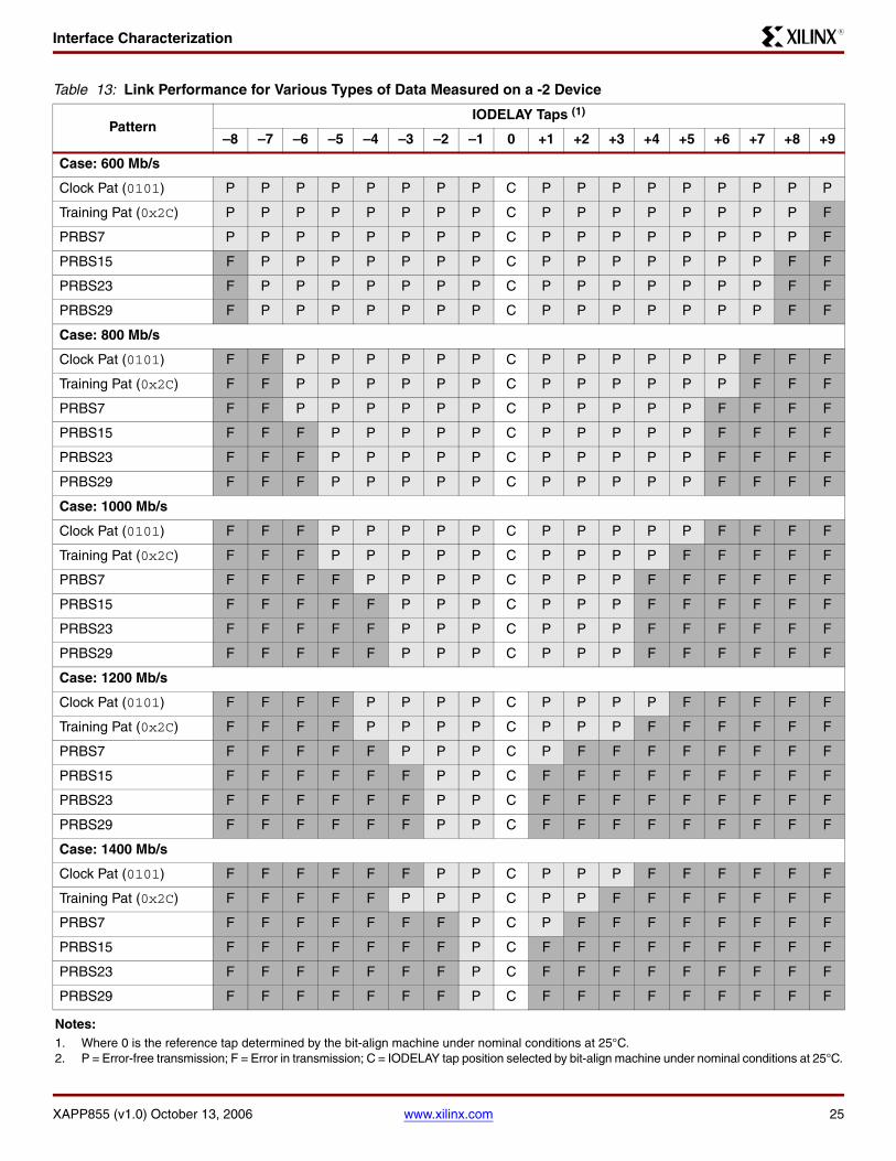
Interface Characterization
XAPP855 (v10) October 13 2006 wwwxilinxcom 25
R
Table 13 Link Performance for Various Types of Data Measured on a -2 Device
PatternIODELAY Taps (1)
ndash8 ndash7 ndash6 ndash5 ndash4 ndash3 ndash2 ndash1 0 +1 +2 +3 +4 +5 +6 +7 +8 +9
Case 600 Mbs
Clock Pat (0101) P P P P P P P P C P P P P P P P P P
Training Pat (0x2C) P P P P P P P P C P P P P P P P P F
PRBS7 P P P P P P P P C P P P P P P P P F
PRBS15 F P P P P P P P C P P P P P P P F F
PRBS23 F P P P P P P P C P P P P P P P F F
PRBS29 F P P P P P P P C P P P P P P P F F
Case 800 Mbs
Clock Pat (0101) F F P P P P P P C P P P P P P F F F
Training Pat (0x2C) F F P P P P P P C P P P P P P F F F
PRBS7 F F P P P P P P C P P P P P F F F F
PRBS15 F F F P P P P P C P P P P P F F F F
PRBS23 F F F P P P P P C P P P P P F F F F
PRBS29 F F F P P P P P C P P P P P F F F F
Case 1000 Mbs
Clock Pat (0101) F F F P P P P P C P P P P P F F F F
Training Pat (0x2C) F F F P P P P P C P P P P F F F F F
PRBS7 F F F F P P P P C P P P F F F F F F
PRBS15 F F F F F P P P C P P P F F F F F F
PRBS23 F F F F F P P P C P P P F F F F F F
PRBS29 F F F F F P P P C P P P F F F F F F
Case 1200 Mbs
Clock Pat (0101) F F F F P P P P C P P P P F F F F F
Training Pat (0x2C) F F F F P P P P C P P P F F F F F F
PRBS7 F F F F F P P P C P F F F F F F F F
PRBS15 F F F F F F P P C F F F F F F F F F
PRBS23 F F F F F F P P C F F F F F F F F F
PRBS29 F F F F F F P P C F F F F F F F F F
Case 1400 Mbs
Clock Pat (0101) F F F F F F P P C P P P F F F F F F
Training Pat (0x2C) F F F F F P P P C P P F F F F F F F
PRBS7 F F F F F F F P C P F F F F F F F F
PRBS15 F F F F F F F P C F F F F F F F F F
PRBS23 F F F F F F F P C F F F F F F F F F
PRBS29 F F F F F F F P C F F F F F F F F F
Notes 1 Where 0 is the reference tap determined by the bit-align machine under nominal conditions at 25degC2 P = Error-free transmission F = Error in transmission C = IODELAY tap position selected by bit-align machine under nominal conditions at 25degC
Resetting the Interface
XAPP855 (v10) October 13 2006 wwwxilinxcom 26
R
Resetting the Interface
Several dependencies determine the order in which circuits should be reset in the interface The receiver cannot begin the alignment algorithm if the transmitter is not sending the training pattern The transmitter must be reset before the receiver and time must be allowed for the training pattern to propagate across the link before the receiver comes out of reset The receiver also cannot begin the alignment algorithm until IDELAYCTRL has recovered from reset which could takes hundreds of cycles The recommended reset timing for the interface is shown in Figure 16 This reset timing is implemented in the BERT testbench for this interface
The TX reset (RST_TX) is used to reset all TX circuitry and also IDELAYCTRL The IDELAYCTRL reset is asynchronous so driving it with RST_TX is acceptable The minimum pulse width of IDELAYCTRL reset is 50 ns (TIDELAYCTRL_RPW) For that reason resets are held High for 16 clock cycles The RX reset (RST_RX) is used to reset all RX circuitry and is asserted when the IDELAYCTRL READY flag goes High indicating that the IODELAY blocks are calibrated
The timing of the READY flag in Figure 16 is a potential hazard Most likely it is High during a TX reset because it takes many cycles for IDELAYCTRL to deassert the READY flag It is easy to make the mistake of resetting the receiver too early To avoid this hazard the RX reset should be asserted only after seeing a deassertion and reassertion of the READY flag
Conclusion Based on the design and characterization described in this document the 16-Channel DDR reference design operates to the performance targets in Table 14 under all conditions of process voltage and temperature However to meet these targets over voltage and temperature the timing budget must be guaranteed according to the analysis in ldquoInterface Timing Budgetrdquo See ldquoAppendixrdquo page 27 for further justification of the maximum performance recommendations in Table 14
Figure 16 Recommended Interface Reset Timing
RST_TX
IDELAYCTRLREADY
RST_RX
16 Cycles X855_16_072406
Table 14 Performance of 16-Channel DDR Interface
Speed Grade Maximum Performance
-1 800 Mbs
-2 900 Mbs
-3 10 Gbs(1)
Notes 1 To achieve higher performance (up to 125 Gbs) see 16-channel DDR LVDS Interface with Realtime
Window Monitoring for an example of a DDR interface with real-time window monitoring
Appendix
XAPP855 (v10) October 13 2006 wwwxilinxcom 27
R
Appendix Performance Characterization Data
Refer to ldquoInterface Characterizationrdquo page 19 for explanations about how to interpret the data in the ldquoAppendixrdquo These tables show collective data eyes for the entire interface over process voltage and temperature (PVT) Three devices from each speed grade were selected for this characterization
The calibrated center position of the eye (marked by the C in the tables below) varies slightly from channel to channel (due to small skews between channels) That range is referred to as center tap range Analysis of Table 16 page 28 through Table 20 page 40 shows that the center tap range for slow and fast parts differ significantly at the same data rate (because the BIT_ALIGN_MACHINE algorithm adjusts for differences in speed)
All data in the ldquoAppendixrdquo is collected using the BERT testbench shown in Figure 2 page 2 The data pattern is PRBS23 and the devicepackage is XC5VLX50T-FF1136 The transmission path for the cases shown in Table 16 through Table 20 is repeated for convenience
TX rarr 5 FR-4 rarr SAMTEC QSE Conn rarr 12 Ribbon Cable rarr SAMTEC QSE Conn rarr 5 FR-4 rarr RX
A summary of these characterization results is shown in Table 15 Each of the nine parts were tested at 800 900 1000 1100 and 1200 Mbs When the interface is error free on all channels under all extreme conditions of temperature and voltage the particular test case is designated by a P A test case is marked FAIL when the interface suffered errors on any channel under any particular condition of voltage and temperature
Table 15 Summary of Interface Characterization Results
Device (SN) Speed Grade 800 Mbs 900 Mbs 1000Mbs 1100 Mbs 1200 Mbs
2194 -1 P P P FAIL FAIL
2219 -1 P FAIL FAIL FAIL FAIL
2199 -1 P P FAIL FAIL FAIL
001 -2 P P FAIL P FAIL
002 -2 P P P P FAIL
003 -2 P P FAIL FAIL FAIL
004 -3 P P P P P
005 -3 P P P P P
006 -3 P P P P P
Appendix
XAPP855 (v10) October 13 2006 wwwxilinxcom 28
R
Table 16 Measurement of Receiver Drift under Extreme Conditions at 800 Mbs
ConditionIODELAY Taps (1)
ndash8 ndash7 ndash6 ndash5 ndash4 ndash3 ndash2 ndash1 0 +1 +2 +3 +4 +5 +6 +7 +8
SN 2194 Speed Grade -1
25degC Nom Supplies F F F P P P P P C P P P P F F F F
0degC Nom Supplies F F F P P P P P P P P P P F F F F
85degC Nom Supplies F F F F P P P P P P P P P F F F F
25degC +5 Supplies F F P P P P P P P P P P F F F F F
0degC +5 Supplies F F P P P P P P P P P P F F F F F
85degC +5 Supplies F F P P P P P P P P P P F F F F F
25degC ndash5 Supplies F F F F F F P P P P P P P P P F F
0degC ndash5 Supplies F F F F F F P P P P P P P P P F F
85degC ndash5 Supplies F F F F F F P P P P P P P P P F F
Center Tap Range Taps 11ndash12
CONCLUSION Error free under all conditions when calibrated under nominal conditions to position C
SN 2219 Speed Grade -1
25degC Nom Supplies F F F P P P P P C P P P F F F F F
0degC Nom Supplies F F F P P P P P P P P P F F F F F
85degC Nom Supplies F F F P P P P P P P P P F F F F F
25degC +5 Supplies F P P P P P P P P P P F F F F F F
0degC +5 Supplies F P P P P P P P P P P F F F F F F
85degC +5 Supplies F P P P P P P P P P P F F F F F F
25degC ndash5 Supplies F F F F F F P P P P P P P P F F F
0degC ndash5 Supplies F F F F F F F P P P P P P P F F F
85degC ndash5 Supplies F F F F F F P P P P P P P P F F F
Center Tap Range Taps 13ndash16
CONCLUSION Error free under all conditions when calibrated under nominal conditions to position C
SN 2199 Speed Grade -1
25degC Nom Supplies F F F P P P P P C P P P P F F F F
0degC Nom Supplies F F F P P P P P P P P P P F F F F
85degC Nom Supplies F F F P P P P P P P P P P F F F F
25degC +5 Supplies F P P P P P P P P P P P F F F F F
0degC +5 Supplies F P P P P P P P P P P P F F F F F
85degC +5 Supplies F P P P P P P P P P P P F F F F F
25degC ndash5 Supplies F F F F F F P P P P P P P P P F F
0degC ndash5 Supplies F F F F F F P P P P P P P P P F F
85degC ndash5 Supplies F F F F F F P P P P P P P P P F F
Center Tap Range Taps 10ndash12
CONCLUSION Error free under all conditions when calibrated under nominal conditions to position C
Appendix
XAPP855 (v10) October 13 2006 wwwxilinxcom 29
R
SN 001 Speed Grade -2
25degC Nom Supplies F F F P P P P P C P P P P F F F F
0degC Nom Supplies F F F P P P P P P P P P P F F F F
85degC Nom Supplies F F F P P P P P P P P P P F F F F
25degC +5 Supplies F P P P P P P P P P P P F F F F F
0degC +5 Supplies F P P P P P P P P P P F F F F F F
85degC +5 Supplies F P P P P P P P P P P P F F F F F
25degC ndash5 Supplies F F F F F P P P P P P P P P P F F
0degC ndash5 Supplies F F F F F P P P P P P P P P P F F
85degC ndash5 Supplies F F F F F P P P P P P P P P P F F
Center Tap Range Taps 10ndash12
CONCLUSION Error free under all conditions when calibrated under nominal conditions to position C
SN 002 Speed Grade -2
25degC Nom Supplies F F F P P P P P C P P P P F F F F
0degC Nom Supplies F F F P P P P P P P P P P F F F F
85degC Nom Supplies F F F P P P P P P P P P P F F F F
25degC +5 Supplies F P P P P P P P P P P P F F F F F
0degC +5 Supplies F P P P P P P P P P P P F F F F F
85degC +5 Supplies F F P P P P P P P P P P F F F F F
25degC ndash5 Supplies F F F F F P P P P P P P P P P F F
0degC ndash5 Supplies F F F F F P P P P P P P P P P F F
85degC ndash5 Supplies F F F F F P P P P P P P P P P F F
Center Tap Range Taps 10ndash12
CONCLUSION Error free under all conditions when calibrated under nominal conditions to position C
SN 003 Speed Grade -2
25degC Nom Supplies F F F P P P P P C P P P P F F F F
0degC Nom Supplies F F F P P P P P P P P P P F F F F
85degC Nom Supplies F F F P P P P P P P P P P F F F F
25degC +5 Supplies F P P P P P P P P P P P F F F F F
0degC +5 Supplies F P P P P P P P P P P F F F F F F
85degC +5 Supplies F P P P P P P P P P P P F F F F F
25degC ndash5 Supplies F F F F F F P P P P P P P P P F F
0degC ndash5 Supplies F F F F F F P P P P P P P P P F F
85degC ndash5 Supplies F F F F F F P P P P P P P P P F F
Center Tap Range Taps 11ndash13
CONCLUSION Error free under all conditions when calibrated under nominal conditions to position C
Table 16 Measurement of Receiver Drift under Extreme Conditions at 800 Mbs (Continued)
ConditionIODELAY Taps (1)
ndash8 ndash7 ndash6 ndash5 ndash4 ndash3 ndash2 ndash1 0 +1 +2 +3 +4 +5 +6 +7 +8
Appendix
XAPP855 (v10) October 13 2006 wwwxilinxcom 30
R
SN 004 Speed Grade -3
25degC Nom Supplies F F F P P P P P C P P P P F F F F
0degC Nom Supplies F F F P P P P P P P P P F F F F F
85degC Nom Supplies F F F P P P P P P P P P P F F F F
25degC +5 Supplies F P P P P P P P P P P P F F F F F
0degC +5 Supplies F P P P P P P P P P P P F F F F F
85degC +5 Supplies F F P P P P P P P P P P F F F F F
25degC ndash5 Supplies F F F F F P P P P P P P P P F F F
0degC ndash5 Supplies F F F F F P P P P P P P P P F F F
85degC ndash5 Supplies F F F F F P P P P P P P P P F F F
Center Tap Range Taps 8ndash9 23ndash24
CONCLUSION Error free under all conditions when calibrated under nominal conditions to position C
SN 005 Speed Grade -3
25degC Nom Supplies F F P P P P P P C P P P P F F F F
0degC Nom Supplies F F P P P P P P P P P P P F F F F
85degC Nom Supplies F F F P P P P P P P P P P P F F F
25degC +5 Supplies F P P P P P P P P P P P F F F F F
0degC +5 Supplies F P P P P P P P P P P P F F F F F
85degC +5 Supplies F P P P P P P P P P P P F F F F F
25degC ndash5 Supplies F F F F P P P P P P P P P P P F F
0degC ndash5 Supplies F F F F P P P P P P P P P P P F F
85degC ndash5 Supplies F F F F P P P P P P P P P P P F F
Center Tap Range Taps 9ndash10
CONCLUSION Error free under all conditions when calibrated under nominal conditions to position C
SN 006 Speed Grade -3
25degC Nom Supplies F F P P P P P P C P P P P F F F F
0degC Nom Supplies F F P P P P P P P P P P P F F F F
85degC Nom Supplies F F F P P P P P P P P P P F F F F
25degC +5 Supplies F P P P P P P P P P P P F F F F F
0degC +5 Supplies F P P P P P P P P P P P F F F F F
85degC +5 Supplies F F P P P P P P P P P P F F F F F
25degC ndash5 Supplies F F F P P P P P P P P P P P F F F
0degC ndash5 Supplies F F F P P P P P P P P P P P F F F
85degC ndash5 Supplies F F F F F P P P P P P P P P F F F
Center Tap Range Taps 8ndash9 23ndash24
CONCLUSION Error free under all conditions when calibrated under nominal conditions to position C
Notes 1 IODELAY taps where 0 is the reference tap determined by the bit align machine at nominal voltage and 25degC2 P = Error-free transmission F = Error in transmission C = IODELAY tap position selected by bit-align machine under nominal conditions at 25degC
Table 16 Measurement of Receiver Drift under Extreme Conditions at 800 Mbs (Continued)
ConditionIODELAY Taps (1)
ndash8 ndash7 ndash6 ndash5 ndash4 ndash3 ndash2 ndash1 0 +1 +2 +3 +4 +5 +6 +7 +8
Appendix
XAPP855 (v10) October 13 2006 wwwxilinxcom 31
R
Table 17 Measurement of Receiver Drift under Extreme Conditions at 900 Mbs
ConditionIODELAY Taps (1)
ndash8 ndash7 ndash6 ndash5 ndash4 ndash3 ndash2 ndash1 0 +1 +2 +3 +4 +5 +6 +7 +8
SN 2194 Speed Grade -1
25degC Nom Supplies F F F F F P P P C P P P F F F F F
0degC Nom Supplies F F F F F P P P P P P P F F F F F
85degC Nom Supplies F F F F F P P P P P P P P F F F F
25degC +5 Supplies F F F P P P P P P P P F F F F F F
0degC +5 Supplies F F F P P P P P P P P F F F F F F
85degC +5 Supplies F F F P P P P P P P P F F F F F F
25degC ndash5 Supplies F F F F F F F P P P P P P P F F F
0degC ndash5 Supplies F F F F F F F P P P P P P P F F F
85degC ndash5 Supplies F F F F F F F P P P P P P P F F F
Center Tap Range Taps 11ndash12
CONCLUSION Error free under all conditions when calibrated under nominal conditions to position C
SN 2219 Speed Grade -1
25degC Nom Supplies F F F F F P P P C P P P F F F F F
0degC Nom Supplies F F F F F P P P P P P P F F F F F
85degC Nom Supplies F F F F F P P P P P P P F F F F F
25degC +5 Supplies F F F P P P P P P P F F F F F F F
0degC +5 Supplies F F F P P P P P P P F F F F F F F
85degC +5 Supplies F F F P P P P P P P F F F F F F F
25degC ndash5 Supplies F F F F F F F F F P P P P P F F F
0degC ndash5 Supplies F F F F F F F F F P P P P P F F F
85degC ndash5 Supplies F F F F F F F F P P P P P P F F F
Center Tap Range Taps 12ndash15
CONCLUSION Errors caused by ndash5 variation in supply voltage
SN 2199 Speed Grade -1
25degC Nom Supplies F F F F F P P P C P P P F F F F F
0degC Nom Supplies F F F F F P P P P P P P F F F F F
85degC Nom Supplies F F F F F P P P P P P P F F F F F
25degC +5 Supplies F F F P P P P P P P P F F F F F F
0degC +5 Supplies F F F P P P P P P P P F F F F F F
85degC +5 Supplies F F F P P P P P P P P F F F F F F
25degC ndash5 Supplies F F F F F F F F P P P P P P F F F
0degC ndash5 Supplies F F F F F F F F P P P P P P F F F
85degC ndash5 Supplies F F F F F F F F P P P P P P F F F
Center Tap Range Taps 10ndash12
CONCLUSION Error free under all conditions when calibrated under nominal conditions to position C
Appendix
XAPP855 (v10) October 13 2006 wwwxilinxcom 32
R
SN 001 Speed Grade -2
25degC Nom Supplies F F F F P P P P C P P P P F F F F
0degC Nom Supplies F F F F P P P P P P P P P F F F F
85degC Nom Supplies F F F F F P P P P P P P P F F F F
25degC +5 Supplies F F P P P P P P P P P F F F F F F
0degC +5 Supplies F F P P P P P P P P P F F F F F F
85degC +5 Supplies F F F P P P P P P P P P F F F F F
25degC ndash5 Supplies F F F F F F F P P P P P P P F F F
0degC ndash5 Supplies F F F F F F F P P P P P P P F F F
85degC ndash5 Supplies F F F F F F F P P P P P P P F F F
Center Tap Range Taps 9ndash11
CONCLUSION Error free under all conditions when calibrated under nominal conditions to position C
SN 002 Speed Grade -2
25degC Nom Supplies F F F F P P P P C P P P P F F F F
0degC Nom Supplies F F F F P P P P P P P P F F F F F
85degC Nom Supplies F F F F F P P P P P P P P F F F F
25degC +5 Supplies F F F P P P P P P P P F F F F F F
0degC +5 Supplies F F F P P P P P P P P F F F F F F
85degC +5 Supplies F F F P P P P P P P P P F F F F F
25degC ndash5 Supplies F F F F F F F P P P P P P P F F F
0degC ndash5 Supplies F F F F F F F P P P P P P P F F F
85degC ndash5 Supplies F F F F F F F P P P P P P P F F F
Center Tap Range Taps 10ndash12
CONCLUSION Error free under all conditions when calibrated under nominal conditions to position C
SN 003 Speed Grade -2
25degC Nom Supplies F F F F F P P P C P P P P F F F F
0degC Nom Supplies F F F F F P P P P P P P P F F F F
85degC Nom Supplies F F F F F P P P P P P P P F F F F
25degC +5 Supplies F F P P P P P P P P P F F F F F F
0degC +5 Supplies F F P P P P P P P P P F F F F F F
85degC +5 Supplies F F F P P P P P P P P F F F F F F
25degC ndash5 Supplies F F F F F F F P P P P P P P F F F
0degC ndash5 Supplies F F F F F F F F P P P P P P F F F
85degC ndash5 Supplies F F F F F F F P P P P P P P F F F
Center Tap Range Taps 11ndash13
CONCLUSION Error free under all conditions when calibrated under nominal conditions to position C
Table 17 Measurement of Receiver Drift under Extreme Conditions at 900 Mbs (Continued)
ConditionIODELAY Taps (1)
ndash8 ndash7 ndash6 ndash5 ndash4 ndash3 ndash2 ndash1 0 +1 +2 +3 +4 +5 +6 +7 +8
Appendix
XAPP855 (v10) October 13 2006 wwwxilinxcom 33
R
SN 004 Speed Grade -3
25degC Nom Supplies F F F F P P P P C P P P P F F F F
0degC Nom Supplies F F F P P P P P P P P P P F F F F
85degC Nom Supplies F F F F P P P P P P P P P F F F F
25degC +5 Supplies F F F P P P P P P P P P F F F F F
0degC +5 Supplies F F F P P P P P P P P P F F F F F
85degC +5 Supplies F F F P P P P P P P P P F F F F F
25degC ndash5 Supplies F F F F F F P P P P P P P P F F F
0degC ndash5 Supplies F F F F F F P P P P P P P P F F F
85degC ndash5 Supplies F F F F F F P P P P P P P P F F F
Center Tap Range Taps 7ndash8
CONCLUSION Error free under all conditions when calibrated under nominal conditions to position C
SN 005 Speed Grade ndash3
25degC Nom Supplies F F F P P P P P C P P P P F F F F
0degC Nom Supplies F F F P P P P P P P P P P F F F F
85degC Nom Supplies F F F F P P P P P P P P P F F F F
25degC +5 Supplies F F P P P P P P P P P P F F F F F
0degC +5 Supplies F F P P P P P P P P P P F F F F F
85degC +5 Supplies F F F P P P P P P P P P F F F F F
25degC ndash5 Supplies F F F F F F P P P P P P P P F F F
0degC ndash5 Supplies F F F F F P P P P P P P P P F F F
85degC ndash5 Supplies F F F F F F P P P P P P P P F F F
Center Tap Range Taps 9ndash10
CONCLUSION Error free under all conditions when calibrated under nominal conditions to position C
SN 006 Speed Grade -3
25degC Nom Supplies F F F F P P P P C P P P P F F F F
0degC Nom Supplies F F F F P P P P P P P P P F F F F
85degC Nom Supplies F F F F P P P P P P P P P F F F F
25degC +5 Supplies F F P P P P P P P P P P F F F F F
0degC +5 Supplies F F P P P P P P P P P P F F F F F
85degC +5 Supplies F F F P P P P P P P P P F F F F F
25degC ndash5 Supplies F F F F F P P P P P P P P P F F F
0degC ndash5 Supplies F F F F F P P P P P P P P P F F F
85degC ndash5 Supplies F F F F F F P P P P P P P P F F F
Center Tap Range Taps 7ndash8
CONCLUSION Error free under all conditions when calibrated under nominal conditions to position C
Notes 1 IODELAY taps where 0 is the reference tap determined by the bit align machine at nominal voltage and 25degC2 P = Error-free transmission F = Error in transmission C = IODELAY tap position selected by bit-align machine under nominal conditions at 25degC
Table 17 Measurement of Receiver Drift under Extreme Conditions at 900 Mbs (Continued)
ConditionIODELAY Taps (1)
ndash8 ndash7 ndash6 ndash5 ndash4 ndash3 ndash2 ndash1 0 +1 +2 +3 +4 +5 +6 +7 +8
Appendix
XAPP855 (v10) October 13 2006 wwwxilinxcom 34
R
Table 18 Measurement of Receiver Drift under Extreme Conditions at 1000 Mbs
ConditionIODELAY Taps (1)
ndash8 ndash7 ndash6 ndash5 ndash4 ndash3 ndash2 ndash1 0 +1 +2 +3 +4 +5 +6 +7 +8
SN 2194 Speed Grade -1
25degC Nom Supplies F F F F F P P P C P P F F F F F F
0degC Nom Supplies F F F F F P P P P P P F F F F F F
85degC Nom Supplies F F F F F P P P P P P F F F F F F
25degC +5 Supplies F F F P P P P P P P F F F F F F F
0degC +5 Supplies F F F P P P P P P P F F F F F F F
85degC +5 Supplies F F F F P P P P P P F F F F F F F
25degC ndash5 Supplies F F F F F F F F P P P P P F F F F
0degC ndash5 Supplies F F F F F F F F P P P P P F F F F
85degC ndash5 Supplies F F F F F F F F P P P P P F F F F
Center Tap Range Taps 12ndash13
CONCLUSION Error free under all conditions when calibrated under nominal conditions to position C
SN 2219 Speed Grade -1
25degC Nom Supplies F F F F F F P P C P P F F F F F F
0degC Nom Supplies F F F F F F P P P P P F F F F F F
85degC Nom Supplies F F F F F F P P P P P F F F F F F
25degC +5 Supplies F F F P P P P P P F F F F F F F F
0degC +5 Supplies F F F P P P P P P F F F F F F F F
85degC +5 Supplies F F F F P P P P P F F F F F F F F
25degC ndash5 Supplies F F F F F F F F F P P P P F F F F
0degC ndash5 Supplies F F F F F F F F F F P P P F F F F
85degC ndash5 Supplies F F F F F F F F F P P P P F F F F
Center Tap Range Taps 14ndash17
CONCLUSION Errors caused by ndash5 variation in supply voltage
SN 2199 Speed Grade -1
25degC Nom Supplies F F F F F F P P C P P F F F F F F
0degC Nom Supplies F F F F F F P P P P P F F F F F F
85degC Nom Supplies F F F F F F P P P P P F F F F F F
25degC +5 Supplies F F F F P P P P P P F F F F F F F
0degC +5 Supplies F F F F P P P P P P F F F F F F F
85degC +5 Supplies F F F F P P P P P P F F F F F F F
25degC ndash5 Supplies F F F F F F F F F P P P P F F F F
0degC ndash5 Supplies F F F F F F F F F P P P P F F F F
85degC ndash5 Supplies F F F F F F F F F P P P P F F F F
Center Tap Range Taps 12ndash14
CONCLUSION Errors caused by ndash5 variation in supply voltage
Appendix
XAPP855 (v10) October 13 2006 wwwxilinxcom 35
R
SN 001 Speed Grade -2
25degC Nom Supplies F F F F F F P P C P P P F F F F F
0degC Nom Supplies F F F F F F P P P P P P F F F F F
85degC Nom Supplies F F F F F F P P P P P P F F F F F
25degC +5 Supplies F F F F P P P P P P F F F F F F F
0degC +5 Supplies F F F F P P P P P P F F F F F F F
85degC +5 Supplies F F F F P P P P P P P F F F F F F
25degC ndash5 Supplies F F F F F F F F F P P P P F F F F
0degC ndash5 Supplies F F F F F F F F F P P P P F F F F
85degC ndash5 Supplies F F F F F F F F F P P P P F F F F
Center Tap Range Taps 11ndash12
CONCLUSION Errors caused by ndash5 variation in supply voltage
SN 002 Speed Grade -2
25degC Nom Supplies F F F F F P P P C P P F F F F F F
0degC Nom Supplies F F F F F P P P P P P P F F F F F
85degC Nom Supplies F F F F F P P P P P P P F F F F F
25degC +5 Supplies F F F F P P P P P P F F F F F F F
0degC +5 Supplies F F F P P P P P P P F F F F F F F
85degC +5 Supplies F F F F P P P P P P P F F F F F F
25degC ndash5 Supplies F F F F F F F P P P P P P F F F F
0degC ndash5 Supplies F F F F F F F P P P P P P F F F F
85degC ndash5 Supplies F F F F F F F P P P P P P F F F F
Center Tap Range Taps 11ndash13
CONCLUSION Error free under all conditions when calibrated under nominal conditions to position C
SN 003 Speed Grade -2
25degC Nom Supplies F F F F F F P P C P P F F F F F F
0degC Nom Supplies F F F F F F P P P P P F F F F F F
85degC Nom Supplies F F F F F F P P P P P F F F F F F
25degC +5 Supplies F F F F P P P P P P F F F F F F F
0degC +5 Supplies F F F F P P P P P P F F F F F F F
85degC +5 Supplies F F F F P P P P P P F F F F F F F
25degC ndash5 Supplies F F F F F F F F F P P P P F F F F
0degC ndash5 Supplies F F F F F F F F F P P P P F F F F
85degC ndash5 Supplies F F F F F F F F F P P P P F F F F
Center Tap Range Taps 13ndash14
CONCLUSION Errors caused by ndash5 variation in supply voltage
Table 18 Measurement of Receiver Drift under Extreme Conditions at 1000 Mbs (Continued)
ConditionIODELAY Taps (1)
ndash8 ndash7 ndash6 ndash5 ndash4 ndash3 ndash2 ndash1 0 +1 +2 +3 +4 +5 +6 +7 +8
Appendix
XAPP855 (v10) October 13 2006 wwwxilinxcom 36
R
SN 004 Speed Grade -3
25degC Nom Supplies F F F F F P P P C P P P F F F F F
0degC Nom Supplies F F F F F P P P P P P P F F F F F
85degC Nom Supplies F F F F F P P P P P P P F F F F F
25degC +5 Supplies F F F P P P P P P P P F F F F F F
0degC +5 Supplies F F F P P P P P P P P F F F F F F
85degC +5 Supplies F F F F P P P P P P P P F F F F F
25degC ndash5 Supplies F F F F F F F P P P P P P F F F F
0degC ndash5 Supplies F F F F F F F P P P P P P F F F F
85degC ndash5 Supplies F F F F F F F P P P P P P P F F F
Center Tap Range Taps 9ndash10
CONCLUSION Error free under all conditions when calibrated under nominal conditions to position C
SN 005 Speed Grade -3
25degC Nom Supplies F F F F P P P P C P P P F F F F F
0degC Nom Supplies F F F F P P P P P P P P F F F F F
85degC Nom Supplies F F F F P P P P P P P P F F F F F
25degC +5 Supplies F F F P P P P P P P P F F F F F F
0degC +5 Supplies F F P P P P P P P P P F F F F F F
85degC +5 Supplies F F F P P P P P P P P F F F F F F
25degC ndash5 Supplies F F F F F F P P P P P P P P F F F
0degC ndash5 Supplies F F F F F F P P P P P P P P F F F
85degC ndash5 Supplies F F F F F F P P P P P P P F F F F
Center Tap Range Taps 11ndash12
CONCLUSION Error free under all conditions when calibrated under nominal conditions to position C
SN 006 Speed Grade -3
25degC Nom Supplies F F F F P P P P C P P P F F F F F
0degC Nom Supplies F F F F P P P P P P P P F F F F F
85degC Nom Supplies F F F F P P P P P P P P F F F F F
25degC +5 Supplies F F F P P P P P P P P F F F F F F
0degC +5 Supplies F F F P P P P P P P P F F F F F F
85degC +5 Supplies F F F P P P P P P P P F F F F F F
25degC ndash5 Supplies F F F F F F P P P P P P P F F F F
0degC ndash5 Supplies F F F F F F P P P P P P P F F F F
85degC ndash5 Supplies F F F F F F P P P P P P P F F F F
Center Tap Range Taps 9ndash10
CONCLUSION Error free under all conditions when calibrated under nominal conditions to position C
Notes 1 IODELAY taps where 0 is the reference tap determined by the bit align machine at nominal voltage and 25degC2 P = Error-free transmission F = Error in transmission C = IODELAY tap position selected by bit-align machine under nominal conditions at 25degC
Table 18 Measurement of Receiver Drift under Extreme Conditions at 1000 Mbs (Continued)
ConditionIODELAY Taps (1)
ndash8 ndash7 ndash6 ndash5 ndash4 ndash3 ndash2 ndash1 0 +1 +2 +3 +4 +5 +6 +7 +8
Appendix
XAPP855 (v10) October 13 2006 wwwxilinxcom 37
R
Table 19 Measurement of Receiver Drift under Extreme Conditions at 1100 Mbs
ConditionIODELAY Taps (1)
ndash8 ndash7 ndash6 ndash5 ndash4 ndash3 ndash2 ndash1 0 +1 +2 +3 +4 +5 +6 +7 +8
SN 2194 Speed Grade -1
25degC Nom Supplies F F F F F F P P C P P F F F F F F
0degC Nom Supplies F F F F F F P P P P P F F F F F F
85degC Nom Supplies F F F F F F P P P P P F F F F F F
25degC +5 Supplies F F F F P P P P P F F F F F F F F
0degC +5 Supplies F F F F P P P P P F F F F F F F F
85degC +5 Supplies F F F F P P P P P F F F F F F F F
25degC ndash5 Supplies F F F F F F F F F P P P F F F F F
0degC ndash5 Supplies F F F F F F F F F P P P F F F F F
85degC ndash5 Supplies F F F F F F F F F P P P F F F F F
Center Tap Range Taps 13ndash14
CONCLUSION Errors caused by ndash5 variation in supply voltage
SN 2219 Speed Grade -1
25degC Nom Supplies F F F F F F P P C P F F F F F F F
0degC Nom Supplies F F F F F F P P P P F F F F F F F
85degC Nom Supplies F F F F F F P P P P F F F F F F F
25degC +5 Supplies F F F F P P P P F F F F F F F F F
0degC +5 Supplies F F F F P P P P F F F F F F F F F
85degC +5 Supplies F F F F P P P P F F F F F F F F F
25degC ndash5 Supplies F F F F F F F F F F P P F F F F F
0degC ndash5 Supplies F F F F F F F F F F P P F F F F F
85degC ndash5 Supplies F F F F F F F F F P P P F F F F F
Center Tap Range Taps 6 15ndash17
CONCLUSION Errors caused by plusmn5 variation in supply voltage
SN 2199 Speed Grade -1
25degC Nom Supplies F F F F F F F P C P F F F F F F F
0degC Nom Supplies F F F F F F F P P P F F F F F F F
85degC Nom Supplies F F F F F F F P P P F F F F F F F
25degC +5 Supplies F F F F P P P P P F F F F F F F F
0degC +5 Supplies F F F F P P P P P F F F F F F F F
85degC +5 Supplies F F F F F P P P P F F F F F F F F
25degC ndash5 Supplies F F F F F F F F F F P P F F F F F
0degC ndash5 Supplies F F F F F F F F F F P P F F F F F
85degC ndash5 Supplies F F F F F F F F F F P P F F F F F
Center Tap Range Taps 13ndash15
CONCLUSION Errors caused by ndash5 variation in supply voltage
Appendix
XAPP855 (v10) October 13 2006 wwwxilinxcom 38
R
SN 001 Speed Grade -2
25degC Nom Supplies F F F F F F P P C P P F F F F F F
0degC Nom Supplies F F F F F F P P P P P F F F F F F
85degC Nom Supplies F F F F F F P P P P P F F F F F F
25degC +5 Supplies F F F F P P P P P F F F F F F F F
0degC +5 Supplies F F F F P P P P P F F F F F F F F
85degC +5 Supplies F F F F P P P P P F F F F F F F F
25degC ndash5 Supplies F F F F F F F F P P P P F F F F F
0degC ndash5 Supplies F F F F F F F F P P P P F F F F F
85degC ndash5 Supplies F F F F F F F F P P P P F F F F F
Center Tap Range Taps 12ndash13
CONCLUSION Error free under all conditions when calibrated under nominal conditions to position C
SN 002 Speed Grade -2
25degC Nom Supplies F F F F F P P P C P F F F F F F F
0degC Nom Supplies F F F F F P P P P P F F F F F F F
85degC Nom Supplies F F F F F F P P P P F F F F F F F
25degC +5 Supplies F F F F P P P P P F F F F F F F F
0degC +5 Supplies F F F P P P P P P F F F F F F F F
85degC +5 Supplies F F F F P P P P P F F F F F F F F
25degC ndash5 Supplies F F F F F F F F P P P P F F F F F
0degC ndash5 Supplies F F F F F F F F P P P P F F F F F
85degC ndash5 Supplies F F F F F F F F P P P P F F F F F
Center Tap Range Taps 13ndash14
CONCLUSION Error free under all conditions when calibrated under nominal conditions to position C
SN 003 Speed Grade -2
25degC Nom Supplies F F F F F F F P C P F F F F F F F
0degC Nom Supplies F F F F F F F P P P F F F F F F F
85degC Nom Supplies F F F F F F F P P P P F F F F F F
25degC +5 Supplies F F F F F P P P P F F F F F F F F
0degC +5 Supplies F F F F F P P P P F F F F F F F F
85degC +5 Supplies F F F F F P P P P F F F F F F F F
25degC ndash5 Supplies F F F F F F F F F F P P F F F F F
0degC ndash5 Supplies F F F F F F F F F F P P F F F F F
85degC ndash5 Supplies F F F F F F F F F P P P F F F F F
Center Tap Range Taps 14ndash16
CONCLUSION Errors caused by ndash5 variation in supply voltage
Table 19 Measurement of Receiver Drift under Extreme Conditions at 1100 Mbs (Continued)
ConditionIODELAY Taps (1)
ndash8 ndash7 ndash6 ndash5 ndash4 ndash3 ndash2 ndash1 0 +1 +2 +3 +4 +5 +6 +7 +8
Appendix
XAPP855 (v10) October 13 2006 wwwxilinxcom 39
R
SN 004 Speed Grade -3
25degC Nom Supplies F F F F F P P P C P P F F F F F F
0degC Nom Supplies F F F F F P P P P P P F F F F F F
85degC Nom Supplies F F F F F F P P P P P F F F F F F
25degC +5 Supplies F F F F P P P P P P F F F F F F F
0degC +5 Supplies F F F F P P P P P P F F F F F F F
85degC +5 Supplies F F F F P P P P P P F F F F F F F
25degC ndash5 Supplies F F F F F F F F P P P P F F F F F
0degC ndash5 Supplies F F F F F F F P P P P P F F F F F
85degC ndash5 Supplies F F F F F F F F P P P P P F F F F
Center Tap Range Taps 9ndash10
CONCLUSION Error free under all conditions when calibrated under nominal conditions to position C
SN 005 Speed Grade -3
25degC Nom Supplies F F F F F P P P C P P F F F F F F
0degC Nom Supplies F F F F F P P P P P P F F F F F F
85degC Nom Supplies F F F F F F P P P P P F F F F F F
25degC +5 Supplies F F F F P P P P P P F F F F F F F
0degC +5 Supplies F F F F P P P P P P F F F F F F F
85degC +5 Supplies F F F F P P P P P P F F F F F F F
25degC ndash5 Supplies F F F F F F F P P P P P P F F F F
0degC ndash5 Supplies F F F F F F F P P P P P P F F F F
85degC ndash5 Supplies F F F F F F F P P P P P P F F F F
Center Tap Range Taps 11ndash12
CONCLUSION Error free under all conditions when calibrated under nominal conditions to position C
SN 006 Speed Grade -3
25degC Nom Supplies F F F F F P P P C P P P F F F F F
0degC Nom Supplies F F F F F P P P P P P F F F F F F
85degC Nom Supplies F F F F F P P P P P P P F F F F F
25degC +5 Supplies F F F F P P P P P P P F F F F F F
0degC +5 Supplies F F F P P P P P P P F F F F F F F
85degC +5 Supplies F F F F P P P P P P P F F F F F F
25degC ndash5 Supplies F F F F F F P P P P P P P F F F F
0degC ndash5 Supplies F F F F F F P P P P P P P F F F F
85degC ndash5 Supplies F F F F F F F P P P P P P F F F F
Center Tap Range Taps 9ndash10
CONCLUSION Error free under all conditions when calibrated under nominal conditions to position C
Notes 1 IODELAY taps where 0 is the reference tap determined by the bit align machine at nominal voltage and 25degC2 P = Error-free transmission F = Error in transmission C = IODELAY tap position selected by bit-align machine under nominal conditions at 25degC
Table 19 Measurement of Receiver Drift under Extreme Conditions at 1100 Mbs (Continued)
ConditionIODELAY Taps (1)
ndash8 ndash7 ndash6 ndash5 ndash4 ndash3 ndash2 ndash1 0 +1 +2 +3 +4 +5 +6 +7 +8
Appendix
XAPP855 (v10) October 13 2006 wwwxilinxcom 40
R
Table 20 Measurement of Receiver Drift under Extreme Conditions at 1200 Mbs
ConditionIODELAY Taps (1)
ndash8 ndash7 ndash6 ndash5 ndash4 ndash3 ndash2 ndash1 0 +1 +2 +3 +4 +5 +6 +7 +8
SN 2194 Speed Grade -1
25degC Nom Supplies F F F F F F F P C F F F F F F F F
0degC Nom Supplies F F F F F F F P P F F F F F F F F
85degC Nom Supplies F F F F F F F P P F F F F F F F F
25degC +5 Supplies F F F F P P P P F F F F F F F F F
0degC +5 Supplies F F F F P P P P F F F F F F F F F
85degC +5 Supplies F F F F F P P P F F F F F F F F F
25degC ndash5 Supplies F F F F F F F F F P P F F F F F F
0degC ndash5 Supplies F F F F F F F F F F P F F F F F F
85degC ndash5 Supplies F F F F F F F F F P F F F F F F F
Center Tap Range Taps 13ndash15
CONCLUSION Errors caused by plusmn5 variation in supply voltage
SN 2219 Speed Grade -1
25degC Nom Supplies F F F F F F F F C F F F F F F F F
0degC Nom Supplies F F F F F F F P P F F F F F F F F
85degC Nom Supplies F F F F F F F F P F F F F F F F F
25degC +5 Supplies F F F F F P P P F F F F F F F F F
0degC +5 Supplies F F F F F P P P F F F F F F F F F
85degC +5 Supplies F F F F F F P P F F F F F F F F F
25degC ndash5 Supplies F F F F F F F F F F F F F F F F F
0degC ndash5 Supplies F F F F F F F F F F F F F F F F F
85degC ndash5 Supplies F F F F F F F F F F F F F F F F F
Center Tap Range Taps 6ndash7 16ndash17
CONCLUSION Errors caused by plusmn5 variation in supply voltage
SN 2199 Speed Grade -1
25degC Nom Supplies F F F F F F F P C F F F F F F F F
0degC Nom Supplies F F F F F F F P P F F F F F F F F
85degC Nom Supplies F F F F F F F F P F F F F F F F F
25degC +5 Supplies F F F F F P P P F F F F F F F F F
0degC +5 Supplies F F F F F P P P F F F F F F F F F
85degC +5 Supplies F F F F F P P P F F F F F F F F F
25degC ndash5 Supplies F F F F F F F F F F F F F F F F F
0degC ndash5 Supplies F F F F F F F F F F F F F F F F F
85degC ndash5 Supplies F F F F F F F F F F F F F F F F F
Center Tap Range Taps 13ndash15
CONCLUSION Errors caused by plusmn5 variation in supply voltage
Appendix
XAPP855 (v10) October 13 2006 wwwxilinxcom 41
R
SN 001 Speed Grade -2
25degC Nom Supplies F F F F F F F P C P F F F F F F F
0degC Nom Supplies F F F F F F F P P P F F F F F F F
85degC Nom Supplies F F F F F F F P P P F F F F F F F
25degC +5 Supplies F F F F F P P P P F F F F F F F F
0degC +5 Supplies F F F F P P P P P F F F F F F F F
85degC +5 Supplies F F F F F P P P P F F F F F F F F
25degC ndash5 Supplies F F F F F F F F F F P F F F F F F
0degC ndash5 Supplies F F F F F F F F F F P F F F F F F
85degC ndash5 Supplies F F F F F F F F F F P F F F F F F
Center Tap Range Taps 12ndash13
CONCLUSION Errors caused by ndash5 variation in supply voltage
SN 002 Speed Grade -2
25degC Nom Supplies F F F F F F P P C P F F F F F F F
0degC Nom Supplies F F F F F F P P P P F F F F F F F
85degC Nom Supplies F F F F F F F P P P F F F F F F F
25degC +5 Supplies F F F F P P P P F F F F F F F F F
0degC +5 Supplies F F F F P P P P F F F F F F F F F
85degC +5 Supplies F F F F F P P P F F F F F F F F F
25degC ndash5 Supplies F F F F F F F F P P P F F F F F F
0degC ndash5 Supplies F F F F F F F F P P P F F F F F F
85degC ndash5 Supplies F F F F F F F F F P P F F F F F F
Center Tap Range Taps 13ndash14
CONCLUSION Errors caused by plusmn5 variation in supply voltage
SN 003 Speed Grade -2
25degC Nom Supplies F F F F F F F P C F F F F F F F F
0degC Nom Supplies F F F F F F F P P F F F F F F F F
85degC Nom Supplies F F F F F F F F P F F F F F F F F
25degC +5 Supplies F F F F F P P P F F F F F F F F F
0degC +5 Supplies F F F F F P P P F F F F F F F F F
85degC +5 Supplies F F F F F F P P F F F F F F F F F
25degC ndash5 Supplies F F F F F F F F F F F F F F F F F
0degC ndash5 Supplies F F F F F F F F F F F F F F F F F
85degC ndash5 Supplies F F F F F F F F F F F F F F F F F
Center Tap Range Taps 14ndash15
CONCLUSION Errors caused by plusmn5 variation in supply voltage
Table 20 Measurement of Receiver Drift under Extreme Conditions at 1200 Mbs (Continued)
ConditionIODELAY Taps (1)
ndash8 ndash7 ndash6 ndash5 ndash4 ndash3 ndash2 ndash1 0 +1 +2 +3 +4 +5 +6 +7 +8
Appendix
XAPP855 (v10) October 13 2006 wwwxilinxcom 42
R
SN 004 Speed Grade -3
25degC Nom Supplies F F F F F F P P C P F F F F F F F
0degC Nom Supplies F F F F F P P P P P F F F F F F F
85degC Nom Supplies F F F F F F P P P P F F F F F F F
25degC +5 Supplies F F F F P P P P P F F F F F F F F
0degC +5 Supplies F F F F P P P P P F F F F F F F F
85degC +5 Supplies F F F F F P P P P F F F F F F F F
25degC ndash5 Supplies F F F F F F F F P P P F F F F F F
0degC ndash5 Supplies F F F F F F F F P P P F F F F F F
85degC ndash5 Supplies F F F F F F F F P P P F F F F F F
Center Tap Range Taps 9ndash11
CONCLUSION Error free under all conditions when calibrated under nominal conditions to position C
SN 005 Speed Grade -3
25degC Nom Supplies F F F F F P P P C P F F F F F F F
0degC Nom Supplies F F F F F P P P P P F F F F F F F
85degC Nom Supplies F F F F F F P P P P F F F F F F F
25degC +5 Supplies F F F F P P P P P F F F F F F F F
0degC +5 Supplies F F F P P P P P P F F F F F F F F
85degC +5 Supplies F F F F P P P P P F F F F F F F F
25degC ndash5 Supplies F F F F F F F P P P P P F F F F F
0degC ndash5 Supplies F F F F F F F P P P P P F F F F F
85degC ndash5 Supplies F F F F F F F F P P P F F F F F F
Center Tap Range Taps 11ndash13
CONCLUSION Error free under all conditions when calibrated under nominal conditions to position C
SN 006 Speed Grade -3
25degC Nom Supplies F F F F F P P P C P F F F F F F F
0degC Nom Supplies F F F F F P P P P P F F F F F F F
85degC Nom Supplies F F F F F P P P P P F F F F F F F
25degC +5 Supplies F F F P P P P P P F F F F F F F F
0degC +5 Supplies F F F P P P P P P F F F F F F F F
85degC +5 Supplies F F F F P P P P P F F F F F F F F
25degC ndash5 Supplies F F F F F F F P P P P F F F F F F
0degC ndash5 Supplies F F F F F F P P P P P F F F F F F
85degC ndash5 Supplies F F F F F F F P P P P F F F F F F
Center Tap Range Taps 10ndash11
CONCLUSION Error free under all conditions when calibrated under nominal conditions to position C
Notes 1 IODELAY taps where 0 is the reference tap determined by the bit align machine at nominal voltage and 25degC2 P = Error-free transmission F = Error in transmission C = IODELAY tap position selected by bit-align machine under nominal conditions at 25degC
Table 20 Measurement of Receiver Drift under Extreme Conditions at 1200 Mbs (Continued)
ConditionIODELAY Taps (1)
ndash8 ndash7 ndash6 ndash5 ndash4 ndash3 ndash2 ndash1 0 +1 +2 +3 +4 +5 +6 +7 +8
Revision History
XAPP855 (v10) October 13 2006 wwwxilinxcom 43
R
Revision History
The following table shows the revision history for this document
Date Version Revision
101306 10 Initial Xilinx release
- 16-Channel DDR LVDS Interface with Per-Channel Alignment
-
- Summary
- Introduction
-
- Figure 1 Full-Duplex 16-Channel DDR Link between a Virtex-5 Device and Another Device with a 16-Channel DDR Interface
- Figure 2 BERT Testbench for Hardware Verification of the DDR Interface
- Figure 3 Design Hierarchy of the Interface (TX and RX)
-
- DDR Transmitter
-
- Table 1 DDR_8TO1_16CHAN_TX Module Port Definitions
- Figure 4 MasterSlave OSERDES Pair for a Single Data Channel with 81 Serialization
- Figure 5 Block Diagram of TX Interface
- Table 2 DDR TX Interface Utilization Statistics
-
- Interface Clocking
-
- Figure 6 Global and Regional Clocking Schemes in Virtex-5 FPGAs
- Table 3 Comparison of Global and IO Clock Performance by Speed Grade
-
- DDR Receiver
-
- Table 4 DDR_8TO1_16CHAN_RX Module Port Definitions
- Figure 7 MasterSlave ISERDES Pair for a Single Data Channel with 18 Deserialization
- Figure 8 Block Diagram of RX Interface
- Table 5 DDR RX Interface Utilization Statistics
-
- Receiver Interface Dynamic Timing
-
- Inherent Timing
-
- Figure 9 Timing Components of RX Data and Clock Paths
- Figure 10 ISE Timing Analyzer Properties Used in this Document
- Table 6 Datapath Timing Definitions
- Table 7 Clock Path Timing Definitions
- Table 8 Datapath Delay Inventory for a -1 Speed Grade XC5VLX50T Device
- Table 9 Clock Path Delay Inventory for a -1 Speed Grade XC5VLX50T Device
- Figure 11 Timing Windows Show Uncertainty in ClockData Relationship as Calculated by Timing Analyzer
-
- Dynamic Timing and BIT_ALIGN_MACHINE
-
- Figure 12 Inherent Timing Windows Shown in Relation to Multiple Data Rates
- Figure 13 Dynamic Bit-Alignment Procedure in BIT_ALIGN_MACHINE
- Table 10 Word Alignment in the DDR Receiver
- Figure 14 FSM in the BIT_ALIGN_MACHINE Module
-
- Interface Timing Budget
-
- Interface Characterization
-
- Figure 15 Bit-Alignment Algorithm Performance
- Table 11 Tap Setting Range For Various Data Rates Measured on a -2 Device
- Table 12 Measurement of Receiver Drift under Extreme Conditions for Multiple Data Rates
- Pattern Dependence of Receiver Performance
-
- Table 13 Link Performance for Various Types of Data Measured on a -2 Device
-
- Resetting the Interface
-
- Figure 16 Recommended Interface Reset Timing
-
- Conclusion
-
- Table 14 Performance of 16-Channel DDR Interface
-
- Appendix
-
- Performance Characterization Data
-
- Table 15 Summary of Interface Characterization Results
- Table 16 Measurement of Receiver Drift under Extreme Conditions at 800 Mbs
- Table 17 Measurement of Receiver Drift under Extreme Conditions at 900 Mbs
- Table 18 Measurement of Receiver Drift under Extreme Conditions at 1000 Mbs
- Table 19 Measurement of Receiver Drift under Extreme Conditions at 1100 Mbs
- Table 20 Measurement of Receiver Drift under Extreme Conditions at 1200 Mbs
-
- Revision History
-
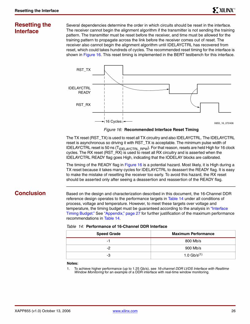
Resetting the Interface
XAPP855 (v10) October 13 2006 wwwxilinxcom 26
R
Resetting the Interface
Several dependencies determine the order in which circuits should be reset in the interface The receiver cannot begin the alignment algorithm if the transmitter is not sending the training pattern The transmitter must be reset before the receiver and time must be allowed for the training pattern to propagate across the link before the receiver comes out of reset The receiver also cannot begin the alignment algorithm until IDELAYCTRL has recovered from reset which could takes hundreds of cycles The recommended reset timing for the interface is shown in Figure 16 This reset timing is implemented in the BERT testbench for this interface
The TX reset (RST_TX) is used to reset all TX circuitry and also IDELAYCTRL The IDELAYCTRL reset is asynchronous so driving it with RST_TX is acceptable The minimum pulse width of IDELAYCTRL reset is 50 ns (TIDELAYCTRL_RPW) For that reason resets are held High for 16 clock cycles The RX reset (RST_RX) is used to reset all RX circuitry and is asserted when the IDELAYCTRL READY flag goes High indicating that the IODELAY blocks are calibrated
The timing of the READY flag in Figure 16 is a potential hazard Most likely it is High during a TX reset because it takes many cycles for IDELAYCTRL to deassert the READY flag It is easy to make the mistake of resetting the receiver too early To avoid this hazard the RX reset should be asserted only after seeing a deassertion and reassertion of the READY flag
Conclusion Based on the design and characterization described in this document the 16-Channel DDR reference design operates to the performance targets in Table 14 under all conditions of process voltage and temperature However to meet these targets over voltage and temperature the timing budget must be guaranteed according to the analysis in ldquoInterface Timing Budgetrdquo See ldquoAppendixrdquo page 27 for further justification of the maximum performance recommendations in Table 14
Figure 16 Recommended Interface Reset Timing
RST_TX
IDELAYCTRLREADY
RST_RX
16 Cycles X855_16_072406
Table 14 Performance of 16-Channel DDR Interface
Speed Grade Maximum Performance
-1 800 Mbs
-2 900 Mbs
-3 10 Gbs(1)
Notes 1 To achieve higher performance (up to 125 Gbs) see 16-channel DDR LVDS Interface with Realtime
Window Monitoring for an example of a DDR interface with real-time window monitoring
Appendix
XAPP855 (v10) October 13 2006 wwwxilinxcom 27
R
Appendix Performance Characterization Data
Refer to ldquoInterface Characterizationrdquo page 19 for explanations about how to interpret the data in the ldquoAppendixrdquo These tables show collective data eyes for the entire interface over process voltage and temperature (PVT) Three devices from each speed grade were selected for this characterization
The calibrated center position of the eye (marked by the C in the tables below) varies slightly from channel to channel (due to small skews between channels) That range is referred to as center tap range Analysis of Table 16 page 28 through Table 20 page 40 shows that the center tap range for slow and fast parts differ significantly at the same data rate (because the BIT_ALIGN_MACHINE algorithm adjusts for differences in speed)
All data in the ldquoAppendixrdquo is collected using the BERT testbench shown in Figure 2 page 2 The data pattern is PRBS23 and the devicepackage is XC5VLX50T-FF1136 The transmission path for the cases shown in Table 16 through Table 20 is repeated for convenience
TX rarr 5 FR-4 rarr SAMTEC QSE Conn rarr 12 Ribbon Cable rarr SAMTEC QSE Conn rarr 5 FR-4 rarr RX
A summary of these characterization results is shown in Table 15 Each of the nine parts were tested at 800 900 1000 1100 and 1200 Mbs When the interface is error free on all channels under all extreme conditions of temperature and voltage the particular test case is designated by a P A test case is marked FAIL when the interface suffered errors on any channel under any particular condition of voltage and temperature
Table 15 Summary of Interface Characterization Results
Device (SN) Speed Grade 800 Mbs 900 Mbs 1000Mbs 1100 Mbs 1200 Mbs
2194 -1 P P P FAIL FAIL
2219 -1 P FAIL FAIL FAIL FAIL
2199 -1 P P FAIL FAIL FAIL
001 -2 P P FAIL P FAIL
002 -2 P P P P FAIL
003 -2 P P FAIL FAIL FAIL
004 -3 P P P P P
005 -3 P P P P P
006 -3 P P P P P
Appendix
XAPP855 (v10) October 13 2006 wwwxilinxcom 28
R
Table 16 Measurement of Receiver Drift under Extreme Conditions at 800 Mbs
ConditionIODELAY Taps (1)
ndash8 ndash7 ndash6 ndash5 ndash4 ndash3 ndash2 ndash1 0 +1 +2 +3 +4 +5 +6 +7 +8
SN 2194 Speed Grade -1
25degC Nom Supplies F F F P P P P P C P P P P F F F F
0degC Nom Supplies F F F P P P P P P P P P P F F F F
85degC Nom Supplies F F F F P P P P P P P P P F F F F
25degC +5 Supplies F F P P P P P P P P P P F F F F F
0degC +5 Supplies F F P P P P P P P P P P F F F F F
85degC +5 Supplies F F P P P P P P P P P P F F F F F
25degC ndash5 Supplies F F F F F F P P P P P P P P P F F
0degC ndash5 Supplies F F F F F F P P P P P P P P P F F
85degC ndash5 Supplies F F F F F F P P P P P P P P P F F
Center Tap Range Taps 11ndash12
CONCLUSION Error free under all conditions when calibrated under nominal conditions to position C
SN 2219 Speed Grade -1
25degC Nom Supplies F F F P P P P P C P P P F F F F F
0degC Nom Supplies F F F P P P P P P P P P F F F F F
85degC Nom Supplies F F F P P P P P P P P P F F F F F
25degC +5 Supplies F P P P P P P P P P P F F F F F F
0degC +5 Supplies F P P P P P P P P P P F F F F F F
85degC +5 Supplies F P P P P P P P P P P F F F F F F
25degC ndash5 Supplies F F F F F F P P P P P P P P F F F
0degC ndash5 Supplies F F F F F F F P P P P P P P F F F
85degC ndash5 Supplies F F F F F F P P P P P P P P F F F
Center Tap Range Taps 13ndash16
CONCLUSION Error free under all conditions when calibrated under nominal conditions to position C
SN 2199 Speed Grade -1
25degC Nom Supplies F F F P P P P P C P P P P F F F F
0degC Nom Supplies F F F P P P P P P P P P P F F F F
85degC Nom Supplies F F F P P P P P P P P P P F F F F
25degC +5 Supplies F P P P P P P P P P P P F F F F F
0degC +5 Supplies F P P P P P P P P P P P F F F F F
85degC +5 Supplies F P P P P P P P P P P P F F F F F
25degC ndash5 Supplies F F F F F F P P P P P P P P P F F
0degC ndash5 Supplies F F F F F F P P P P P P P P P F F
85degC ndash5 Supplies F F F F F F P P P P P P P P P F F
Center Tap Range Taps 10ndash12
CONCLUSION Error free under all conditions when calibrated under nominal conditions to position C
Appendix
XAPP855 (v10) October 13 2006 wwwxilinxcom 29
R
SN 001 Speed Grade -2
25degC Nom Supplies F F F P P P P P C P P P P F F F F
0degC Nom Supplies F F F P P P P P P P P P P F F F F
85degC Nom Supplies F F F P P P P P P P P P P F F F F
25degC +5 Supplies F P P P P P P P P P P P F F F F F
0degC +5 Supplies F P P P P P P P P P P F F F F F F
85degC +5 Supplies F P P P P P P P P P P P F F F F F
25degC ndash5 Supplies F F F F F P P P P P P P P P P F F
0degC ndash5 Supplies F F F F F P P P P P P P P P P F F
85degC ndash5 Supplies F F F F F P P P P P P P P P P F F
Center Tap Range Taps 10ndash12
CONCLUSION Error free under all conditions when calibrated under nominal conditions to position C
SN 002 Speed Grade -2
25degC Nom Supplies F F F P P P P P C P P P P F F F F
0degC Nom Supplies F F F P P P P P P P P P P F F F F
85degC Nom Supplies F F F P P P P P P P P P P F F F F
25degC +5 Supplies F P P P P P P P P P P P F F F F F
0degC +5 Supplies F P P P P P P P P P P P F F F F F
85degC +5 Supplies F F P P P P P P P P P P F F F F F
25degC ndash5 Supplies F F F F F P P P P P P P P P P F F
0degC ndash5 Supplies F F F F F P P P P P P P P P P F F
85degC ndash5 Supplies F F F F F P P P P P P P P P P F F
Center Tap Range Taps 10ndash12
CONCLUSION Error free under all conditions when calibrated under nominal conditions to position C
SN 003 Speed Grade -2
25degC Nom Supplies F F F P P P P P C P P P P F F F F
0degC Nom Supplies F F F P P P P P P P P P P F F F F
85degC Nom Supplies F F F P P P P P P P P P P F F F F
25degC +5 Supplies F P P P P P P P P P P P F F F F F
0degC +5 Supplies F P P P P P P P P P P F F F F F F
85degC +5 Supplies F P P P P P P P P P P P F F F F F
25degC ndash5 Supplies F F F F F F P P P P P P P P P F F
0degC ndash5 Supplies F F F F F F P P P P P P P P P F F
85degC ndash5 Supplies F F F F F F P P P P P P P P P F F
Center Tap Range Taps 11ndash13
CONCLUSION Error free under all conditions when calibrated under nominal conditions to position C
Table 16 Measurement of Receiver Drift under Extreme Conditions at 800 Mbs (Continued)
ConditionIODELAY Taps (1)
ndash8 ndash7 ndash6 ndash5 ndash4 ndash3 ndash2 ndash1 0 +1 +2 +3 +4 +5 +6 +7 +8
Appendix
XAPP855 (v10) October 13 2006 wwwxilinxcom 30
R
SN 004 Speed Grade -3
25degC Nom Supplies F F F P P P P P C P P P P F F F F
0degC Nom Supplies F F F P P P P P P P P P F F F F F
85degC Nom Supplies F F F P P P P P P P P P P F F F F
25degC +5 Supplies F P P P P P P P P P P P F F F F F
0degC +5 Supplies F P P P P P P P P P P P F F F F F
85degC +5 Supplies F F P P P P P P P P P P F F F F F
25degC ndash5 Supplies F F F F F P P P P P P P P P F F F
0degC ndash5 Supplies F F F F F P P P P P P P P P F F F
85degC ndash5 Supplies F F F F F P P P P P P P P P F F F
Center Tap Range Taps 8ndash9 23ndash24
CONCLUSION Error free under all conditions when calibrated under nominal conditions to position C
SN 005 Speed Grade -3
25degC Nom Supplies F F P P P P P P C P P P P F F F F
0degC Nom Supplies F F P P P P P P P P P P P F F F F
85degC Nom Supplies F F F P P P P P P P P P P P F F F
25degC +5 Supplies F P P P P P P P P P P P F F F F F
0degC +5 Supplies F P P P P P P P P P P P F F F F F
85degC +5 Supplies F P P P P P P P P P P P F F F F F
25degC ndash5 Supplies F F F F P P P P P P P P P P P F F
0degC ndash5 Supplies F F F F P P P P P P P P P P P F F
85degC ndash5 Supplies F F F F P P P P P P P P P P P F F
Center Tap Range Taps 9ndash10
CONCLUSION Error free under all conditions when calibrated under nominal conditions to position C
SN 006 Speed Grade -3
25degC Nom Supplies F F P P P P P P C P P P P F F F F
0degC Nom Supplies F F P P P P P P P P P P P F F F F
85degC Nom Supplies F F F P P P P P P P P P P F F F F
25degC +5 Supplies F P P P P P P P P P P P F F F F F
0degC +5 Supplies F P P P P P P P P P P P F F F F F
85degC +5 Supplies F F P P P P P P P P P P F F F F F
25degC ndash5 Supplies F F F P P P P P P P P P P P F F F
0degC ndash5 Supplies F F F P P P P P P P P P P P F F F
85degC ndash5 Supplies F F F F F P P P P P P P P P F F F
Center Tap Range Taps 8ndash9 23ndash24
CONCLUSION Error free under all conditions when calibrated under nominal conditions to position C
Notes 1 IODELAY taps where 0 is the reference tap determined by the bit align machine at nominal voltage and 25degC2 P = Error-free transmission F = Error in transmission C = IODELAY tap position selected by bit-align machine under nominal conditions at 25degC
Table 16 Measurement of Receiver Drift under Extreme Conditions at 800 Mbs (Continued)
ConditionIODELAY Taps (1)
ndash8 ndash7 ndash6 ndash5 ndash4 ndash3 ndash2 ndash1 0 +1 +2 +3 +4 +5 +6 +7 +8
Appendix
XAPP855 (v10) October 13 2006 wwwxilinxcom 31
R
Table 17 Measurement of Receiver Drift under Extreme Conditions at 900 Mbs
ConditionIODELAY Taps (1)
ndash8 ndash7 ndash6 ndash5 ndash4 ndash3 ndash2 ndash1 0 +1 +2 +3 +4 +5 +6 +7 +8
SN 2194 Speed Grade -1
25degC Nom Supplies F F F F F P P P C P P P F F F F F
0degC Nom Supplies F F F F F P P P P P P P F F F F F
85degC Nom Supplies F F F F F P P P P P P P P F F F F
25degC +5 Supplies F F F P P P P P P P P F F F F F F
0degC +5 Supplies F F F P P P P P P P P F F F F F F
85degC +5 Supplies F F F P P P P P P P P F F F F F F
25degC ndash5 Supplies F F F F F F F P P P P P P P F F F
0degC ndash5 Supplies F F F F F F F P P P P P P P F F F
85degC ndash5 Supplies F F F F F F F P P P P P P P F F F
Center Tap Range Taps 11ndash12
CONCLUSION Error free under all conditions when calibrated under nominal conditions to position C
SN 2219 Speed Grade -1
25degC Nom Supplies F F F F F P P P C P P P F F F F F
0degC Nom Supplies F F F F F P P P P P P P F F F F F
85degC Nom Supplies F F F F F P P P P P P P F F F F F
25degC +5 Supplies F F F P P P P P P P F F F F F F F
0degC +5 Supplies F F F P P P P P P P F F F F F F F
85degC +5 Supplies F F F P P P P P P P F F F F F F F
25degC ndash5 Supplies F F F F F F F F F P P P P P F F F
0degC ndash5 Supplies F F F F F F F F F P P P P P F F F
85degC ndash5 Supplies F F F F F F F F P P P P P P F F F
Center Tap Range Taps 12ndash15
CONCLUSION Errors caused by ndash5 variation in supply voltage
SN 2199 Speed Grade -1
25degC Nom Supplies F F F F F P P P C P P P F F F F F
0degC Nom Supplies F F F F F P P P P P P P F F F F F
85degC Nom Supplies F F F F F P P P P P P P F F F F F
25degC +5 Supplies F F F P P P P P P P P F F F F F F
0degC +5 Supplies F F F P P P P P P P P F F F F F F
85degC +5 Supplies F F F P P P P P P P P F F F F F F
25degC ndash5 Supplies F F F F F F F F P P P P P P F F F
0degC ndash5 Supplies F F F F F F F F P P P P P P F F F
85degC ndash5 Supplies F F F F F F F F P P P P P P F F F
Center Tap Range Taps 10ndash12
CONCLUSION Error free under all conditions when calibrated under nominal conditions to position C
Appendix
XAPP855 (v10) October 13 2006 wwwxilinxcom 32
R
SN 001 Speed Grade -2
25degC Nom Supplies F F F F P P P P C P P P P F F F F
0degC Nom Supplies F F F F P P P P P P P P P F F F F
85degC Nom Supplies F F F F F P P P P P P P P F F F F
25degC +5 Supplies F F P P P P P P P P P F F F F F F
0degC +5 Supplies F F P P P P P P P P P F F F F F F
85degC +5 Supplies F F F P P P P P P P P P F F F F F
25degC ndash5 Supplies F F F F F F F P P P P P P P F F F
0degC ndash5 Supplies F F F F F F F P P P P P P P F F F
85degC ndash5 Supplies F F F F F F F P P P P P P P F F F
Center Tap Range Taps 9ndash11
CONCLUSION Error free under all conditions when calibrated under nominal conditions to position C
SN 002 Speed Grade -2
25degC Nom Supplies F F F F P P P P C P P P P F F F F
0degC Nom Supplies F F F F P P P P P P P P F F F F F
85degC Nom Supplies F F F F F P P P P P P P P F F F F
25degC +5 Supplies F F F P P P P P P P P F F F F F F
0degC +5 Supplies F F F P P P P P P P P F F F F F F
85degC +5 Supplies F F F P P P P P P P P P F F F F F
25degC ndash5 Supplies F F F F F F F P P P P P P P F F F
0degC ndash5 Supplies F F F F F F F P P P P P P P F F F
85degC ndash5 Supplies F F F F F F F P P P P P P P F F F
Center Tap Range Taps 10ndash12
CONCLUSION Error free under all conditions when calibrated under nominal conditions to position C
SN 003 Speed Grade -2
25degC Nom Supplies F F F F F P P P C P P P P F F F F
0degC Nom Supplies F F F F F P P P P P P P P F F F F
85degC Nom Supplies F F F F F P P P P P P P P F F F F
25degC +5 Supplies F F P P P P P P P P P F F F F F F
0degC +5 Supplies F F P P P P P P P P P F F F F F F
85degC +5 Supplies F F F P P P P P P P P F F F F F F
25degC ndash5 Supplies F F F F F F F P P P P P P P F F F
0degC ndash5 Supplies F F F F F F F F P P P P P P F F F
85degC ndash5 Supplies F F F F F F F P P P P P P P F F F
Center Tap Range Taps 11ndash13
CONCLUSION Error free under all conditions when calibrated under nominal conditions to position C
Table 17 Measurement of Receiver Drift under Extreme Conditions at 900 Mbs (Continued)
ConditionIODELAY Taps (1)
ndash8 ndash7 ndash6 ndash5 ndash4 ndash3 ndash2 ndash1 0 +1 +2 +3 +4 +5 +6 +7 +8
Appendix
XAPP855 (v10) October 13 2006 wwwxilinxcom 33
R
SN 004 Speed Grade -3
25degC Nom Supplies F F F F P P P P C P P P P F F F F
0degC Nom Supplies F F F P P P P P P P P P P F F F F
85degC Nom Supplies F F F F P P P P P P P P P F F F F
25degC +5 Supplies F F F P P P P P P P P P F F F F F
0degC +5 Supplies F F F P P P P P P P P P F F F F F
85degC +5 Supplies F F F P P P P P P P P P F F F F F
25degC ndash5 Supplies F F F F F F P P P P P P P P F F F
0degC ndash5 Supplies F F F F F F P P P P P P P P F F F
85degC ndash5 Supplies F F F F F F P P P P P P P P F F F
Center Tap Range Taps 7ndash8
CONCLUSION Error free under all conditions when calibrated under nominal conditions to position C
SN 005 Speed Grade ndash3
25degC Nom Supplies F F F P P P P P C P P P P F F F F
0degC Nom Supplies F F F P P P P P P P P P P F F F F
85degC Nom Supplies F F F F P P P P P P P P P F F F F
25degC +5 Supplies F F P P P P P P P P P P F F F F F
0degC +5 Supplies F F P P P P P P P P P P F F F F F
85degC +5 Supplies F F F P P P P P P P P P F F F F F
25degC ndash5 Supplies F F F F F F P P P P P P P P F F F
0degC ndash5 Supplies F F F F F P P P P P P P P P F F F
85degC ndash5 Supplies F F F F F F P P P P P P P P F F F
Center Tap Range Taps 9ndash10
CONCLUSION Error free under all conditions when calibrated under nominal conditions to position C
SN 006 Speed Grade -3
25degC Nom Supplies F F F F P P P P C P P P P F F F F
0degC Nom Supplies F F F F P P P P P P P P P F F F F
85degC Nom Supplies F F F F P P P P P P P P P F F F F
25degC +5 Supplies F F P P P P P P P P P P F F F F F
0degC +5 Supplies F F P P P P P P P P P P F F F F F
85degC +5 Supplies F F F P P P P P P P P P F F F F F
25degC ndash5 Supplies F F F F F P P P P P P P P P F F F
0degC ndash5 Supplies F F F F F P P P P P P P P P F F F
85degC ndash5 Supplies F F F F F F P P P P P P P P F F F
Center Tap Range Taps 7ndash8
CONCLUSION Error free under all conditions when calibrated under nominal conditions to position C
Notes 1 IODELAY taps where 0 is the reference tap determined by the bit align machine at nominal voltage and 25degC2 P = Error-free transmission F = Error in transmission C = IODELAY tap position selected by bit-align machine under nominal conditions at 25degC
Table 17 Measurement of Receiver Drift under Extreme Conditions at 900 Mbs (Continued)
ConditionIODELAY Taps (1)
ndash8 ndash7 ndash6 ndash5 ndash4 ndash3 ndash2 ndash1 0 +1 +2 +3 +4 +5 +6 +7 +8
Appendix
XAPP855 (v10) October 13 2006 wwwxilinxcom 34
R
Table 18 Measurement of Receiver Drift under Extreme Conditions at 1000 Mbs
ConditionIODELAY Taps (1)
ndash8 ndash7 ndash6 ndash5 ndash4 ndash3 ndash2 ndash1 0 +1 +2 +3 +4 +5 +6 +7 +8
SN 2194 Speed Grade -1
25degC Nom Supplies F F F F F P P P C P P F F F F F F
0degC Nom Supplies F F F F F P P P P P P F F F F F F
85degC Nom Supplies F F F F F P P P P P P F F F F F F
25degC +5 Supplies F F F P P P P P P P F F F F F F F
0degC +5 Supplies F F F P P P P P P P F F F F F F F
85degC +5 Supplies F F F F P P P P P P F F F F F F F
25degC ndash5 Supplies F F F F F F F F P P P P P F F F F
0degC ndash5 Supplies F F F F F F F F P P P P P F F F F
85degC ndash5 Supplies F F F F F F F F P P P P P F F F F
Center Tap Range Taps 12ndash13
CONCLUSION Error free under all conditions when calibrated under nominal conditions to position C
SN 2219 Speed Grade -1
25degC Nom Supplies F F F F F F P P C P P F F F F F F
0degC Nom Supplies F F F F F F P P P P P F F F F F F
85degC Nom Supplies F F F F F F P P P P P F F F F F F
25degC +5 Supplies F F F P P P P P P F F F F F F F F
0degC +5 Supplies F F F P P P P P P F F F F F F F F
85degC +5 Supplies F F F F P P P P P F F F F F F F F
25degC ndash5 Supplies F F F F F F F F F P P P P F F F F
0degC ndash5 Supplies F F F F F F F F F F P P P F F F F
85degC ndash5 Supplies F F F F F F F F F P P P P F F F F
Center Tap Range Taps 14ndash17
CONCLUSION Errors caused by ndash5 variation in supply voltage
SN 2199 Speed Grade -1
25degC Nom Supplies F F F F F F P P C P P F F F F F F
0degC Nom Supplies F F F F F F P P P P P F F F F F F
85degC Nom Supplies F F F F F F P P P P P F F F F F F
25degC +5 Supplies F F F F P P P P P P F F F F F F F
0degC +5 Supplies F F F F P P P P P P F F F F F F F
85degC +5 Supplies F F F F P P P P P P F F F F F F F
25degC ndash5 Supplies F F F F F F F F F P P P P F F F F
0degC ndash5 Supplies F F F F F F F F F P P P P F F F F
85degC ndash5 Supplies F F F F F F F F F P P P P F F F F
Center Tap Range Taps 12ndash14
CONCLUSION Errors caused by ndash5 variation in supply voltage
Appendix
XAPP855 (v10) October 13 2006 wwwxilinxcom 35
R
SN 001 Speed Grade -2
25degC Nom Supplies F F F F F F P P C P P P F F F F F
0degC Nom Supplies F F F F F F P P P P P P F F F F F
85degC Nom Supplies F F F F F F P P P P P P F F F F F
25degC +5 Supplies F F F F P P P P P P F F F F F F F
0degC +5 Supplies F F F F P P P P P P F F F F F F F
85degC +5 Supplies F F F F P P P P P P P F F F F F F
25degC ndash5 Supplies F F F F F F F F F P P P P F F F F
0degC ndash5 Supplies F F F F F F F F F P P P P F F F F
85degC ndash5 Supplies F F F F F F F F F P P P P F F F F
Center Tap Range Taps 11ndash12
CONCLUSION Errors caused by ndash5 variation in supply voltage
SN 002 Speed Grade -2
25degC Nom Supplies F F F F F P P P C P P F F F F F F
0degC Nom Supplies F F F F F P P P P P P P F F F F F
85degC Nom Supplies F F F F F P P P P P P P F F F F F
25degC +5 Supplies F F F F P P P P P P F F F F F F F
0degC +5 Supplies F F F P P P P P P P F F F F F F F
85degC +5 Supplies F F F F P P P P P P P F F F F F F
25degC ndash5 Supplies F F F F F F F P P P P P P F F F F
0degC ndash5 Supplies F F F F F F F P P P P P P F F F F
85degC ndash5 Supplies F F F F F F F P P P P P P F F F F
Center Tap Range Taps 11ndash13
CONCLUSION Error free under all conditions when calibrated under nominal conditions to position C
SN 003 Speed Grade -2
25degC Nom Supplies F F F F F F P P C P P F F F F F F
0degC Nom Supplies F F F F F F P P P P P F F F F F F
85degC Nom Supplies F F F F F F P P P P P F F F F F F
25degC +5 Supplies F F F F P P P P P P F F F F F F F
0degC +5 Supplies F F F F P P P P P P F F F F F F F
85degC +5 Supplies F F F F P P P P P P F F F F F F F
25degC ndash5 Supplies F F F F F F F F F P P P P F F F F
0degC ndash5 Supplies F F F F F F F F F P P P P F F F F
85degC ndash5 Supplies F F F F F F F F F P P P P F F F F
Center Tap Range Taps 13ndash14
CONCLUSION Errors caused by ndash5 variation in supply voltage
Table 18 Measurement of Receiver Drift under Extreme Conditions at 1000 Mbs (Continued)
ConditionIODELAY Taps (1)
ndash8 ndash7 ndash6 ndash5 ndash4 ndash3 ndash2 ndash1 0 +1 +2 +3 +4 +5 +6 +7 +8
Appendix
XAPP855 (v10) October 13 2006 wwwxilinxcom 36
R
SN 004 Speed Grade -3
25degC Nom Supplies F F F F F P P P C P P P F F F F F
0degC Nom Supplies F F F F F P P P P P P P F F F F F
85degC Nom Supplies F F F F F P P P P P P P F F F F F
25degC +5 Supplies F F F P P P P P P P P F F F F F F
0degC +5 Supplies F F F P P P P P P P P F F F F F F
85degC +5 Supplies F F F F P P P P P P P P F F F F F
25degC ndash5 Supplies F F F F F F F P P P P P P F F F F
0degC ndash5 Supplies F F F F F F F P P P P P P F F F F
85degC ndash5 Supplies F F F F F F F P P P P P P P F F F
Center Tap Range Taps 9ndash10
CONCLUSION Error free under all conditions when calibrated under nominal conditions to position C
SN 005 Speed Grade -3
25degC Nom Supplies F F F F P P P P C P P P F F F F F
0degC Nom Supplies F F F F P P P P P P P P F F F F F
85degC Nom Supplies F F F F P P P P P P P P F F F F F
25degC +5 Supplies F F F P P P P P P P P F F F F F F
0degC +5 Supplies F F P P P P P P P P P F F F F F F
85degC +5 Supplies F F F P P P P P P P P F F F F F F
25degC ndash5 Supplies F F F F F F P P P P P P P P F F F
0degC ndash5 Supplies F F F F F F P P P P P P P P F F F
85degC ndash5 Supplies F F F F F F P P P P P P P F F F F
Center Tap Range Taps 11ndash12
CONCLUSION Error free under all conditions when calibrated under nominal conditions to position C
SN 006 Speed Grade -3
25degC Nom Supplies F F F F P P P P C P P P F F F F F
0degC Nom Supplies F F F F P P P P P P P P F F F F F
85degC Nom Supplies F F F F P P P P P P P P F F F F F
25degC +5 Supplies F F F P P P P P P P P F F F F F F
0degC +5 Supplies F F F P P P P P P P P F F F F F F
85degC +5 Supplies F F F P P P P P P P P F F F F F F
25degC ndash5 Supplies F F F F F F P P P P P P P F F F F
0degC ndash5 Supplies F F F F F F P P P P P P P F F F F
85degC ndash5 Supplies F F F F F F P P P P P P P F F F F
Center Tap Range Taps 9ndash10
CONCLUSION Error free under all conditions when calibrated under nominal conditions to position C
Notes 1 IODELAY taps where 0 is the reference tap determined by the bit align machine at nominal voltage and 25degC2 P = Error-free transmission F = Error in transmission C = IODELAY tap position selected by bit-align machine under nominal conditions at 25degC
Table 18 Measurement of Receiver Drift under Extreme Conditions at 1000 Mbs (Continued)
ConditionIODELAY Taps (1)
ndash8 ndash7 ndash6 ndash5 ndash4 ndash3 ndash2 ndash1 0 +1 +2 +3 +4 +5 +6 +7 +8
Appendix
XAPP855 (v10) October 13 2006 wwwxilinxcom 37
R
Table 19 Measurement of Receiver Drift under Extreme Conditions at 1100 Mbs
ConditionIODELAY Taps (1)
ndash8 ndash7 ndash6 ndash5 ndash4 ndash3 ndash2 ndash1 0 +1 +2 +3 +4 +5 +6 +7 +8
SN 2194 Speed Grade -1
25degC Nom Supplies F F F F F F P P C P P F F F F F F
0degC Nom Supplies F F F F F F P P P P P F F F F F F
85degC Nom Supplies F F F F F F P P P P P F F F F F F
25degC +5 Supplies F F F F P P P P P F F F F F F F F
0degC +5 Supplies F F F F P P P P P F F F F F F F F
85degC +5 Supplies F F F F P P P P P F F F F F F F F
25degC ndash5 Supplies F F F F F F F F F P P P F F F F F
0degC ndash5 Supplies F F F F F F F F F P P P F F F F F
85degC ndash5 Supplies F F F F F F F F F P P P F F F F F
Center Tap Range Taps 13ndash14
CONCLUSION Errors caused by ndash5 variation in supply voltage
SN 2219 Speed Grade -1
25degC Nom Supplies F F F F F F P P C P F F F F F F F
0degC Nom Supplies F F F F F F P P P P F F F F F F F
85degC Nom Supplies F F F F F F P P P P F F F F F F F
25degC +5 Supplies F F F F P P P P F F F F F F F F F
0degC +5 Supplies F F F F P P P P F F F F F F F F F
85degC +5 Supplies F F F F P P P P F F F F F F F F F
25degC ndash5 Supplies F F F F F F F F F F P P F F F F F
0degC ndash5 Supplies F F F F F F F F F F P P F F F F F
85degC ndash5 Supplies F F F F F F F F F P P P F F F F F
Center Tap Range Taps 6 15ndash17
CONCLUSION Errors caused by plusmn5 variation in supply voltage
SN 2199 Speed Grade -1
25degC Nom Supplies F F F F F F F P C P F F F F F F F
0degC Nom Supplies F F F F F F F P P P F F F F F F F
85degC Nom Supplies F F F F F F F P P P F F F F F F F
25degC +5 Supplies F F F F P P P P P F F F F F F F F
0degC +5 Supplies F F F F P P P P P F F F F F F F F
85degC +5 Supplies F F F F F P P P P F F F F F F F F
25degC ndash5 Supplies F F F F F F F F F F P P F F F F F
0degC ndash5 Supplies F F F F F F F F F F P P F F F F F
85degC ndash5 Supplies F F F F F F F F F F P P F F F F F
Center Tap Range Taps 13ndash15
CONCLUSION Errors caused by ndash5 variation in supply voltage
Appendix
XAPP855 (v10) October 13 2006 wwwxilinxcom 38
R
SN 001 Speed Grade -2
25degC Nom Supplies F F F F F F P P C P P F F F F F F
0degC Nom Supplies F F F F F F P P P P P F F F F F F
85degC Nom Supplies F F F F F F P P P P P F F F F F F
25degC +5 Supplies F F F F P P P P P F F F F F F F F
0degC +5 Supplies F F F F P P P P P F F F F F F F F
85degC +5 Supplies F F F F P P P P P F F F F F F F F
25degC ndash5 Supplies F F F F F F F F P P P P F F F F F
0degC ndash5 Supplies F F F F F F F F P P P P F F F F F
85degC ndash5 Supplies F F F F F F F F P P P P F F F F F
Center Tap Range Taps 12ndash13
CONCLUSION Error free under all conditions when calibrated under nominal conditions to position C
SN 002 Speed Grade -2
25degC Nom Supplies F F F F F P P P C P F F F F F F F
0degC Nom Supplies F F F F F P P P P P F F F F F F F
85degC Nom Supplies F F F F F F P P P P F F F F F F F
25degC +5 Supplies F F F F P P P P P F F F F F F F F
0degC +5 Supplies F F F P P P P P P F F F F F F F F
85degC +5 Supplies F F F F P P P P P F F F F F F F F
25degC ndash5 Supplies F F F F F F F F P P P P F F F F F
0degC ndash5 Supplies F F F F F F F F P P P P F F F F F
85degC ndash5 Supplies F F F F F F F F P P P P F F F F F
Center Tap Range Taps 13ndash14
CONCLUSION Error free under all conditions when calibrated under nominal conditions to position C
SN 003 Speed Grade -2
25degC Nom Supplies F F F F F F F P C P F F F F F F F
0degC Nom Supplies F F F F F F F P P P F F F F F F F
85degC Nom Supplies F F F F F F F P P P P F F F F F F
25degC +5 Supplies F F F F F P P P P F F F F F F F F
0degC +5 Supplies F F F F F P P P P F F F F F F F F
85degC +5 Supplies F F F F F P P P P F F F F F F F F
25degC ndash5 Supplies F F F F F F F F F F P P F F F F F
0degC ndash5 Supplies F F F F F F F F F F P P F F F F F
85degC ndash5 Supplies F F F F F F F F F P P P F F F F F
Center Tap Range Taps 14ndash16
CONCLUSION Errors caused by ndash5 variation in supply voltage
Table 19 Measurement of Receiver Drift under Extreme Conditions at 1100 Mbs (Continued)
ConditionIODELAY Taps (1)
ndash8 ndash7 ndash6 ndash5 ndash4 ndash3 ndash2 ndash1 0 +1 +2 +3 +4 +5 +6 +7 +8
Appendix
XAPP855 (v10) October 13 2006 wwwxilinxcom 39
R
SN 004 Speed Grade -3
25degC Nom Supplies F F F F F P P P C P P F F F F F F
0degC Nom Supplies F F F F F P P P P P P F F F F F F
85degC Nom Supplies F F F F F F P P P P P F F F F F F
25degC +5 Supplies F F F F P P P P P P F F F F F F F
0degC +5 Supplies F F F F P P P P P P F F F F F F F
85degC +5 Supplies F F F F P P P P P P F F F F F F F
25degC ndash5 Supplies F F F F F F F F P P P P F F F F F
0degC ndash5 Supplies F F F F F F F P P P P P F F F F F
85degC ndash5 Supplies F F F F F F F F P P P P P F F F F
Center Tap Range Taps 9ndash10
CONCLUSION Error free under all conditions when calibrated under nominal conditions to position C
SN 005 Speed Grade -3
25degC Nom Supplies F F F F F P P P C P P F F F F F F
0degC Nom Supplies F F F F F P P P P P P F F F F F F
85degC Nom Supplies F F F F F F P P P P P F F F F F F
25degC +5 Supplies F F F F P P P P P P F F F F F F F
0degC +5 Supplies F F F F P P P P P P F F F F F F F
85degC +5 Supplies F F F F P P P P P P F F F F F F F
25degC ndash5 Supplies F F F F F F F P P P P P P F F F F
0degC ndash5 Supplies F F F F F F F P P P P P P F F F F
85degC ndash5 Supplies F F F F F F F P P P P P P F F F F
Center Tap Range Taps 11ndash12
CONCLUSION Error free under all conditions when calibrated under nominal conditions to position C
SN 006 Speed Grade -3
25degC Nom Supplies F F F F F P P P C P P P F F F F F
0degC Nom Supplies F F F F F P P P P P P F F F F F F
85degC Nom Supplies F F F F F P P P P P P P F F F F F
25degC +5 Supplies F F F F P P P P P P P F F F F F F
0degC +5 Supplies F F F P P P P P P P F F F F F F F
85degC +5 Supplies F F F F P P P P P P P F F F F F F
25degC ndash5 Supplies F F F F F F P P P P P P P F F F F
0degC ndash5 Supplies F F F F F F P P P P P P P F F F F
85degC ndash5 Supplies F F F F F F F P P P P P P F F F F
Center Tap Range Taps 9ndash10
CONCLUSION Error free under all conditions when calibrated under nominal conditions to position C
Notes 1 IODELAY taps where 0 is the reference tap determined by the bit align machine at nominal voltage and 25degC2 P = Error-free transmission F = Error in transmission C = IODELAY tap position selected by bit-align machine under nominal conditions at 25degC
Table 19 Measurement of Receiver Drift under Extreme Conditions at 1100 Mbs (Continued)
ConditionIODELAY Taps (1)
ndash8 ndash7 ndash6 ndash5 ndash4 ndash3 ndash2 ndash1 0 +1 +2 +3 +4 +5 +6 +7 +8
Appendix
XAPP855 (v10) October 13 2006 wwwxilinxcom 40
R
Table 20 Measurement of Receiver Drift under Extreme Conditions at 1200 Mbs
ConditionIODELAY Taps (1)
ndash8 ndash7 ndash6 ndash5 ndash4 ndash3 ndash2 ndash1 0 +1 +2 +3 +4 +5 +6 +7 +8
SN 2194 Speed Grade -1
25degC Nom Supplies F F F F F F F P C F F F F F F F F
0degC Nom Supplies F F F F F F F P P F F F F F F F F
85degC Nom Supplies F F F F F F F P P F F F F F F F F
25degC +5 Supplies F F F F P P P P F F F F F F F F F
0degC +5 Supplies F F F F P P P P F F F F F F F F F
85degC +5 Supplies F F F F F P P P F F F F F F F F F
25degC ndash5 Supplies F F F F F F F F F P P F F F F F F
0degC ndash5 Supplies F F F F F F F F F F P F F F F F F
85degC ndash5 Supplies F F F F F F F F F P F F F F F F F
Center Tap Range Taps 13ndash15
CONCLUSION Errors caused by plusmn5 variation in supply voltage
SN 2219 Speed Grade -1
25degC Nom Supplies F F F F F F F F C F F F F F F F F
0degC Nom Supplies F F F F F F F P P F F F F F F F F
85degC Nom Supplies F F F F F F F F P F F F F F F F F
25degC +5 Supplies F F F F F P P P F F F F F F F F F
0degC +5 Supplies F F F F F P P P F F F F F F F F F
85degC +5 Supplies F F F F F F P P F F F F F F F F F
25degC ndash5 Supplies F F F F F F F F F F F F F F F F F
0degC ndash5 Supplies F F F F F F F F F F F F F F F F F
85degC ndash5 Supplies F F F F F F F F F F F F F F F F F
Center Tap Range Taps 6ndash7 16ndash17
CONCLUSION Errors caused by plusmn5 variation in supply voltage
SN 2199 Speed Grade -1
25degC Nom Supplies F F F F F F F P C F F F F F F F F
0degC Nom Supplies F F F F F F F P P F F F F F F F F
85degC Nom Supplies F F F F F F F F P F F F F F F F F
25degC +5 Supplies F F F F F P P P F F F F F F F F F
0degC +5 Supplies F F F F F P P P F F F F F F F F F
85degC +5 Supplies F F F F F P P P F F F F F F F F F
25degC ndash5 Supplies F F F F F F F F F F F F F F F F F
0degC ndash5 Supplies F F F F F F F F F F F F F F F F F
85degC ndash5 Supplies F F F F F F F F F F F F F F F F F
Center Tap Range Taps 13ndash15
CONCLUSION Errors caused by plusmn5 variation in supply voltage
Appendix
XAPP855 (v10) October 13 2006 wwwxilinxcom 41
R
SN 001 Speed Grade -2
25degC Nom Supplies F F F F F F F P C P F F F F F F F
0degC Nom Supplies F F F F F F F P P P F F F F F F F
85degC Nom Supplies F F F F F F F P P P F F F F F F F
25degC +5 Supplies F F F F F P P P P F F F F F F F F
0degC +5 Supplies F F F F P P P P P F F F F F F F F
85degC +5 Supplies F F F F F P P P P F F F F F F F F
25degC ndash5 Supplies F F F F F F F F F F P F F F F F F
0degC ndash5 Supplies F F F F F F F F F F P F F F F F F
85degC ndash5 Supplies F F F F F F F F F F P F F F F F F
Center Tap Range Taps 12ndash13
CONCLUSION Errors caused by ndash5 variation in supply voltage
SN 002 Speed Grade -2
25degC Nom Supplies F F F F F F P P C P F F F F F F F
0degC Nom Supplies F F F F F F P P P P F F F F F F F
85degC Nom Supplies F F F F F F F P P P F F F F F F F
25degC +5 Supplies F F F F P P P P F F F F F F F F F
0degC +5 Supplies F F F F P P P P F F F F F F F F F
85degC +5 Supplies F F F F F P P P F F F F F F F F F
25degC ndash5 Supplies F F F F F F F F P P P F F F F F F
0degC ndash5 Supplies F F F F F F F F P P P F F F F F F
85degC ndash5 Supplies F F F F F F F F F P P F F F F F F
Center Tap Range Taps 13ndash14
CONCLUSION Errors caused by plusmn5 variation in supply voltage
SN 003 Speed Grade -2
25degC Nom Supplies F F F F F F F P C F F F F F F F F
0degC Nom Supplies F F F F F F F P P F F F F F F F F
85degC Nom Supplies F F F F F F F F P F F F F F F F F
25degC +5 Supplies F F F F F P P P F F F F F F F F F
0degC +5 Supplies F F F F F P P P F F F F F F F F F
85degC +5 Supplies F F F F F F P P F F F F F F F F F
25degC ndash5 Supplies F F F F F F F F F F F F F F F F F
0degC ndash5 Supplies F F F F F F F F F F F F F F F F F
85degC ndash5 Supplies F F F F F F F F F F F F F F F F F
Center Tap Range Taps 14ndash15
CONCLUSION Errors caused by plusmn5 variation in supply voltage
Table 20 Measurement of Receiver Drift under Extreme Conditions at 1200 Mbs (Continued)
ConditionIODELAY Taps (1)
ndash8 ndash7 ndash6 ndash5 ndash4 ndash3 ndash2 ndash1 0 +1 +2 +3 +4 +5 +6 +7 +8
Appendix
XAPP855 (v10) October 13 2006 wwwxilinxcom 42
R
SN 004 Speed Grade -3
25degC Nom Supplies F F F F F F P P C P F F F F F F F
0degC Nom Supplies F F F F F P P P P P F F F F F F F
85degC Nom Supplies F F F F F F P P P P F F F F F F F
25degC +5 Supplies F F F F P P P P P F F F F F F F F
0degC +5 Supplies F F F F P P P P P F F F F F F F F
85degC +5 Supplies F F F F F P P P P F F F F F F F F
25degC ndash5 Supplies F F F F F F F F P P P F F F F F F
0degC ndash5 Supplies F F F F F F F F P P P F F F F F F
85degC ndash5 Supplies F F F F F F F F P P P F F F F F F
Center Tap Range Taps 9ndash11
CONCLUSION Error free under all conditions when calibrated under nominal conditions to position C
SN 005 Speed Grade -3
25degC Nom Supplies F F F F F P P P C P F F F F F F F
0degC Nom Supplies F F F F F P P P P P F F F F F F F
85degC Nom Supplies F F F F F F P P P P F F F F F F F
25degC +5 Supplies F F F F P P P P P F F F F F F F F
0degC +5 Supplies F F F P P P P P P F F F F F F F F
85degC +5 Supplies F F F F P P P P P F F F F F F F F
25degC ndash5 Supplies F F F F F F F P P P P P F F F F F
0degC ndash5 Supplies F F F F F F F P P P P P F F F F F
85degC ndash5 Supplies F F F F F F F F P P P F F F F F F
Center Tap Range Taps 11ndash13
CONCLUSION Error free under all conditions when calibrated under nominal conditions to position C
SN 006 Speed Grade -3
25degC Nom Supplies F F F F F P P P C P F F F F F F F
0degC Nom Supplies F F F F F P P P P P F F F F F F F
85degC Nom Supplies F F F F F P P P P P F F F F F F F
25degC +5 Supplies F F F P P P P P P F F F F F F F F
0degC +5 Supplies F F F P P P P P P F F F F F F F F
85degC +5 Supplies F F F F P P P P P F F F F F F F F
25degC ndash5 Supplies F F F F F F F P P P P F F F F F F
0degC ndash5 Supplies F F F F F F P P P P P F F F F F F
85degC ndash5 Supplies F F F F F F F P P P P F F F F F F
Center Tap Range Taps 10ndash11
CONCLUSION Error free under all conditions when calibrated under nominal conditions to position C
Notes 1 IODELAY taps where 0 is the reference tap determined by the bit align machine at nominal voltage and 25degC2 P = Error-free transmission F = Error in transmission C = IODELAY tap position selected by bit-align machine under nominal conditions at 25degC
Table 20 Measurement of Receiver Drift under Extreme Conditions at 1200 Mbs (Continued)
ConditionIODELAY Taps (1)
ndash8 ndash7 ndash6 ndash5 ndash4 ndash3 ndash2 ndash1 0 +1 +2 +3 +4 +5 +6 +7 +8
Revision History
XAPP855 (v10) October 13 2006 wwwxilinxcom 43
R
Revision History
The following table shows the revision history for this document
Date Version Revision
101306 10 Initial Xilinx release
- 16-Channel DDR LVDS Interface with Per-Channel Alignment
-
- Summary
- Introduction
-
- Figure 1 Full-Duplex 16-Channel DDR Link between a Virtex-5 Device and Another Device with a 16-Channel DDR Interface
- Figure 2 BERT Testbench for Hardware Verification of the DDR Interface
- Figure 3 Design Hierarchy of the Interface (TX and RX)
-
- DDR Transmitter
-
- Table 1 DDR_8TO1_16CHAN_TX Module Port Definitions
- Figure 4 MasterSlave OSERDES Pair for a Single Data Channel with 81 Serialization
- Figure 5 Block Diagram of TX Interface
- Table 2 DDR TX Interface Utilization Statistics
-
- Interface Clocking
-
- Figure 6 Global and Regional Clocking Schemes in Virtex-5 FPGAs
- Table 3 Comparison of Global and IO Clock Performance by Speed Grade
-
- DDR Receiver
-
- Table 4 DDR_8TO1_16CHAN_RX Module Port Definitions
- Figure 7 MasterSlave ISERDES Pair for a Single Data Channel with 18 Deserialization
- Figure 8 Block Diagram of RX Interface
- Table 5 DDR RX Interface Utilization Statistics
-
- Receiver Interface Dynamic Timing
-
- Inherent Timing
-
- Figure 9 Timing Components of RX Data and Clock Paths
- Figure 10 ISE Timing Analyzer Properties Used in this Document
- Table 6 Datapath Timing Definitions
- Table 7 Clock Path Timing Definitions
- Table 8 Datapath Delay Inventory for a -1 Speed Grade XC5VLX50T Device
- Table 9 Clock Path Delay Inventory for a -1 Speed Grade XC5VLX50T Device
- Figure 11 Timing Windows Show Uncertainty in ClockData Relationship as Calculated by Timing Analyzer
-
- Dynamic Timing and BIT_ALIGN_MACHINE
-
- Figure 12 Inherent Timing Windows Shown in Relation to Multiple Data Rates
- Figure 13 Dynamic Bit-Alignment Procedure in BIT_ALIGN_MACHINE
- Table 10 Word Alignment in the DDR Receiver
- Figure 14 FSM in the BIT_ALIGN_MACHINE Module
-
- Interface Timing Budget
-
- Interface Characterization
-
- Figure 15 Bit-Alignment Algorithm Performance
- Table 11 Tap Setting Range For Various Data Rates Measured on a -2 Device
- Table 12 Measurement of Receiver Drift under Extreme Conditions for Multiple Data Rates
- Pattern Dependence of Receiver Performance
-
- Table 13 Link Performance for Various Types of Data Measured on a -2 Device
-
- Resetting the Interface
-
- Figure 16 Recommended Interface Reset Timing
-
- Conclusion
-
- Table 14 Performance of 16-Channel DDR Interface
-
- Appendix
-
- Performance Characterization Data
-
- Table 15 Summary of Interface Characterization Results
- Table 16 Measurement of Receiver Drift under Extreme Conditions at 800 Mbs
- Table 17 Measurement of Receiver Drift under Extreme Conditions at 900 Mbs
- Table 18 Measurement of Receiver Drift under Extreme Conditions at 1000 Mbs
- Table 19 Measurement of Receiver Drift under Extreme Conditions at 1100 Mbs
- Table 20 Measurement of Receiver Drift under Extreme Conditions at 1200 Mbs
-
- Revision History
-
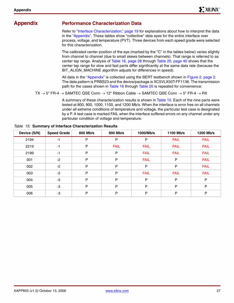
Appendix
XAPP855 (v10) October 13 2006 wwwxilinxcom 27
R
Appendix Performance Characterization Data
Refer to ldquoInterface Characterizationrdquo page 19 for explanations about how to interpret the data in the ldquoAppendixrdquo These tables show collective data eyes for the entire interface over process voltage and temperature (PVT) Three devices from each speed grade were selected for this characterization
The calibrated center position of the eye (marked by the C in the tables below) varies slightly from channel to channel (due to small skews between channels) That range is referred to as center tap range Analysis of Table 16 page 28 through Table 20 page 40 shows that the center tap range for slow and fast parts differ significantly at the same data rate (because the BIT_ALIGN_MACHINE algorithm adjusts for differences in speed)
All data in the ldquoAppendixrdquo is collected using the BERT testbench shown in Figure 2 page 2 The data pattern is PRBS23 and the devicepackage is XC5VLX50T-FF1136 The transmission path for the cases shown in Table 16 through Table 20 is repeated for convenience
TX rarr 5 FR-4 rarr SAMTEC QSE Conn rarr 12 Ribbon Cable rarr SAMTEC QSE Conn rarr 5 FR-4 rarr RX
A summary of these characterization results is shown in Table 15 Each of the nine parts were tested at 800 900 1000 1100 and 1200 Mbs When the interface is error free on all channels under all extreme conditions of temperature and voltage the particular test case is designated by a P A test case is marked FAIL when the interface suffered errors on any channel under any particular condition of voltage and temperature
Table 15 Summary of Interface Characterization Results
Device (SN) Speed Grade 800 Mbs 900 Mbs 1000Mbs 1100 Mbs 1200 Mbs
2194 -1 P P P FAIL FAIL
2219 -1 P FAIL FAIL FAIL FAIL
2199 -1 P P FAIL FAIL FAIL
001 -2 P P FAIL P FAIL
002 -2 P P P P FAIL
003 -2 P P FAIL FAIL FAIL
004 -3 P P P P P
005 -3 P P P P P
006 -3 P P P P P
Appendix
XAPP855 (v10) October 13 2006 wwwxilinxcom 28
R
Table 16 Measurement of Receiver Drift under Extreme Conditions at 800 Mbs
ConditionIODELAY Taps (1)
ndash8 ndash7 ndash6 ndash5 ndash4 ndash3 ndash2 ndash1 0 +1 +2 +3 +4 +5 +6 +7 +8
SN 2194 Speed Grade -1
25degC Nom Supplies F F F P P P P P C P P P P F F F F
0degC Nom Supplies F F F P P P P P P P P P P F F F F
85degC Nom Supplies F F F F P P P P P P P P P F F F F
25degC +5 Supplies F F P P P P P P P P P P F F F F F
0degC +5 Supplies F F P P P P P P P P P P F F F F F
85degC +5 Supplies F F P P P P P P P P P P F F F F F
25degC ndash5 Supplies F F F F F F P P P P P P P P P F F
0degC ndash5 Supplies F F F F F F P P P P P P P P P F F
85degC ndash5 Supplies F F F F F F P P P P P P P P P F F
Center Tap Range Taps 11ndash12
CONCLUSION Error free under all conditions when calibrated under nominal conditions to position C
SN 2219 Speed Grade -1
25degC Nom Supplies F F F P P P P P C P P P F F F F F
0degC Nom Supplies F F F P P P P P P P P P F F F F F
85degC Nom Supplies F F F P P P P P P P P P F F F F F
25degC +5 Supplies F P P P P P P P P P P F F F F F F
0degC +5 Supplies F P P P P P P P P P P F F F F F F
85degC +5 Supplies F P P P P P P P P P P F F F F F F
25degC ndash5 Supplies F F F F F F P P P P P P P P F F F
0degC ndash5 Supplies F F F F F F F P P P P P P P F F F
85degC ndash5 Supplies F F F F F F P P P P P P P P F F F
Center Tap Range Taps 13ndash16
CONCLUSION Error free under all conditions when calibrated under nominal conditions to position C
SN 2199 Speed Grade -1
25degC Nom Supplies F F F P P P P P C P P P P F F F F
0degC Nom Supplies F F F P P P P P P P P P P F F F F
85degC Nom Supplies F F F P P P P P P P P P P F F F F
25degC +5 Supplies F P P P P P P P P P P P F F F F F
0degC +5 Supplies F P P P P P P P P P P P F F F F F
85degC +5 Supplies F P P P P P P P P P P P F F F F F
25degC ndash5 Supplies F F F F F F P P P P P P P P P F F
0degC ndash5 Supplies F F F F F F P P P P P P P P P F F
85degC ndash5 Supplies F F F F F F P P P P P P P P P F F
Center Tap Range Taps 10ndash12
CONCLUSION Error free under all conditions when calibrated under nominal conditions to position C
Appendix
XAPP855 (v10) October 13 2006 wwwxilinxcom 29
R
SN 001 Speed Grade -2
25degC Nom Supplies F F F P P P P P C P P P P F F F F
0degC Nom Supplies F F F P P P P P P P P P P F F F F
85degC Nom Supplies F F F P P P P P P P P P P F F F F
25degC +5 Supplies F P P P P P P P P P P P F F F F F
0degC +5 Supplies F P P P P P P P P P P F F F F F F
85degC +5 Supplies F P P P P P P P P P P P F F F F F
25degC ndash5 Supplies F F F F F P P P P P P P P P P F F
0degC ndash5 Supplies F F F F F P P P P P P P P P P F F
85degC ndash5 Supplies F F F F F P P P P P P P P P P F F
Center Tap Range Taps 10ndash12
CONCLUSION Error free under all conditions when calibrated under nominal conditions to position C
SN 002 Speed Grade -2
25degC Nom Supplies F F F P P P P P C P P P P F F F F
0degC Nom Supplies F F F P P P P P P P P P P F F F F
85degC Nom Supplies F F F P P P P P P P P P P F F F F
25degC +5 Supplies F P P P P P P P P P P P F F F F F
0degC +5 Supplies F P P P P P P P P P P P F F F F F
85degC +5 Supplies F F P P P P P P P P P P F F F F F
25degC ndash5 Supplies F F F F F P P P P P P P P P P F F
0degC ndash5 Supplies F F F F F P P P P P P P P P P F F
85degC ndash5 Supplies F F F F F P P P P P P P P P P F F
Center Tap Range Taps 10ndash12
CONCLUSION Error free under all conditions when calibrated under nominal conditions to position C
SN 003 Speed Grade -2
25degC Nom Supplies F F F P P P P P C P P P P F F F F
0degC Nom Supplies F F F P P P P P P P P P P F F F F
85degC Nom Supplies F F F P P P P P P P P P P F F F F
25degC +5 Supplies F P P P P P P P P P P P F F F F F
0degC +5 Supplies F P P P P P P P P P P F F F F F F
85degC +5 Supplies F P P P P P P P P P P P F F F F F
25degC ndash5 Supplies F F F F F F P P P P P P P P P F F
0degC ndash5 Supplies F F F F F F P P P P P P P P P F F
85degC ndash5 Supplies F F F F F F P P P P P P P P P F F
Center Tap Range Taps 11ndash13
CONCLUSION Error free under all conditions when calibrated under nominal conditions to position C
Table 16 Measurement of Receiver Drift under Extreme Conditions at 800 Mbs (Continued)
ConditionIODELAY Taps (1)
ndash8 ndash7 ndash6 ndash5 ndash4 ndash3 ndash2 ndash1 0 +1 +2 +3 +4 +5 +6 +7 +8
Appendix
XAPP855 (v10) October 13 2006 wwwxilinxcom 30
R
SN 004 Speed Grade -3
25degC Nom Supplies F F F P P P P P C P P P P F F F F
0degC Nom Supplies F F F P P P P P P P P P F F F F F
85degC Nom Supplies F F F P P P P P P P P P P F F F F
25degC +5 Supplies F P P P P P P P P P P P F F F F F
0degC +5 Supplies F P P P P P P P P P P P F F F F F
85degC +5 Supplies F F P P P P P P P P P P F F F F F
25degC ndash5 Supplies F F F F F P P P P P P P P P F F F
0degC ndash5 Supplies F F F F F P P P P P P P P P F F F
85degC ndash5 Supplies F F F F F P P P P P P P P P F F F
Center Tap Range Taps 8ndash9 23ndash24
CONCLUSION Error free under all conditions when calibrated under nominal conditions to position C
SN 005 Speed Grade -3
25degC Nom Supplies F F P P P P P P C P P P P F F F F
0degC Nom Supplies F F P P P P P P P P P P P F F F F
85degC Nom Supplies F F F P P P P P P P P P P P F F F
25degC +5 Supplies F P P P P P P P P P P P F F F F F
0degC +5 Supplies F P P P P P P P P P P P F F F F F
85degC +5 Supplies F P P P P P P P P P P P F F F F F
25degC ndash5 Supplies F F F F P P P P P P P P P P P F F
0degC ndash5 Supplies F F F F P P P P P P P P P P P F F
85degC ndash5 Supplies F F F F P P P P P P P P P P P F F
Center Tap Range Taps 9ndash10
CONCLUSION Error free under all conditions when calibrated under nominal conditions to position C
SN 006 Speed Grade -3
25degC Nom Supplies F F P P P P P P C P P P P F F F F
0degC Nom Supplies F F P P P P P P P P P P P F F F F
85degC Nom Supplies F F F P P P P P P P P P P F F F F
25degC +5 Supplies F P P P P P P P P P P P F F F F F
0degC +5 Supplies F P P P P P P P P P P P F F F F F
85degC +5 Supplies F F P P P P P P P P P P F F F F F
25degC ndash5 Supplies F F F P P P P P P P P P P P F F F
0degC ndash5 Supplies F F F P P P P P P P P P P P F F F
85degC ndash5 Supplies F F F F F P P P P P P P P P F F F
Center Tap Range Taps 8ndash9 23ndash24
CONCLUSION Error free under all conditions when calibrated under nominal conditions to position C
Notes 1 IODELAY taps where 0 is the reference tap determined by the bit align machine at nominal voltage and 25degC2 P = Error-free transmission F = Error in transmission C = IODELAY tap position selected by bit-align machine under nominal conditions at 25degC
Table 16 Measurement of Receiver Drift under Extreme Conditions at 800 Mbs (Continued)
ConditionIODELAY Taps (1)
ndash8 ndash7 ndash6 ndash5 ndash4 ndash3 ndash2 ndash1 0 +1 +2 +3 +4 +5 +6 +7 +8
Appendix
XAPP855 (v10) October 13 2006 wwwxilinxcom 31
R
Table 17 Measurement of Receiver Drift under Extreme Conditions at 900 Mbs
ConditionIODELAY Taps (1)
ndash8 ndash7 ndash6 ndash5 ndash4 ndash3 ndash2 ndash1 0 +1 +2 +3 +4 +5 +6 +7 +8
SN 2194 Speed Grade -1
25degC Nom Supplies F F F F F P P P C P P P F F F F F
0degC Nom Supplies F F F F F P P P P P P P F F F F F
85degC Nom Supplies F F F F F P P P P P P P P F F F F
25degC +5 Supplies F F F P P P P P P P P F F F F F F
0degC +5 Supplies F F F P P P P P P P P F F F F F F
85degC +5 Supplies F F F P P P P P P P P F F F F F F
25degC ndash5 Supplies F F F F F F F P P P P P P P F F F
0degC ndash5 Supplies F F F F F F F P P P P P P P F F F
85degC ndash5 Supplies F F F F F F F P P P P P P P F F F
Center Tap Range Taps 11ndash12
CONCLUSION Error free under all conditions when calibrated under nominal conditions to position C
SN 2219 Speed Grade -1
25degC Nom Supplies F F F F F P P P C P P P F F F F F
0degC Nom Supplies F F F F F P P P P P P P F F F F F
85degC Nom Supplies F F F F F P P P P P P P F F F F F
25degC +5 Supplies F F F P P P P P P P F F F F F F F
0degC +5 Supplies F F F P P P P P P P F F F F F F F
85degC +5 Supplies F F F P P P P P P P F F F F F F F
25degC ndash5 Supplies F F F F F F F F F P P P P P F F F
0degC ndash5 Supplies F F F F F F F F F P P P P P F F F
85degC ndash5 Supplies F F F F F F F F P P P P P P F F F
Center Tap Range Taps 12ndash15
CONCLUSION Errors caused by ndash5 variation in supply voltage
SN 2199 Speed Grade -1
25degC Nom Supplies F F F F F P P P C P P P F F F F F
0degC Nom Supplies F F F F F P P P P P P P F F F F F
85degC Nom Supplies F F F F F P P P P P P P F F F F F
25degC +5 Supplies F F F P P P P P P P P F F F F F F
0degC +5 Supplies F F F P P P P P P P P F F F F F F
85degC +5 Supplies F F F P P P P P P P P F F F F F F
25degC ndash5 Supplies F F F F F F F F P P P P P P F F F
0degC ndash5 Supplies F F F F F F F F P P P P P P F F F
85degC ndash5 Supplies F F F F F F F F P P P P P P F F F
Center Tap Range Taps 10ndash12
CONCLUSION Error free under all conditions when calibrated under nominal conditions to position C
Appendix
XAPP855 (v10) October 13 2006 wwwxilinxcom 32
R
SN 001 Speed Grade -2
25degC Nom Supplies F F F F P P P P C P P P P F F F F
0degC Nom Supplies F F F F P P P P P P P P P F F F F
85degC Nom Supplies F F F F F P P P P P P P P F F F F
25degC +5 Supplies F F P P P P P P P P P F F F F F F
0degC +5 Supplies F F P P P P P P P P P F F F F F F
85degC +5 Supplies F F F P P P P P P P P P F F F F F
25degC ndash5 Supplies F F F F F F F P P P P P P P F F F
0degC ndash5 Supplies F F F F F F F P P P P P P P F F F
85degC ndash5 Supplies F F F F F F F P P P P P P P F F F
Center Tap Range Taps 9ndash11
CONCLUSION Error free under all conditions when calibrated under nominal conditions to position C
SN 002 Speed Grade -2
25degC Nom Supplies F F F F P P P P C P P P P F F F F
0degC Nom Supplies F F F F P P P P P P P P F F F F F
85degC Nom Supplies F F F F F P P P P P P P P F F F F
25degC +5 Supplies F F F P P P P P P P P F F F F F F
0degC +5 Supplies F F F P P P P P P P P F F F F F F
85degC +5 Supplies F F F P P P P P P P P P F F F F F
25degC ndash5 Supplies F F F F F F F P P P P P P P F F F
0degC ndash5 Supplies F F F F F F F P P P P P P P F F F
85degC ndash5 Supplies F F F F F F F P P P P P P P F F F
Center Tap Range Taps 10ndash12
CONCLUSION Error free under all conditions when calibrated under nominal conditions to position C
SN 003 Speed Grade -2
25degC Nom Supplies F F F F F P P P C P P P P F F F F
0degC Nom Supplies F F F F F P P P P P P P P F F F F
85degC Nom Supplies F F F F F P P P P P P P P F F F F
25degC +5 Supplies F F P P P P P P P P P F F F F F F
0degC +5 Supplies F F P P P P P P P P P F F F F F F
85degC +5 Supplies F F F P P P P P P P P F F F F F F
25degC ndash5 Supplies F F F F F F F P P P P P P P F F F
0degC ndash5 Supplies F F F F F F F F P P P P P P F F F
85degC ndash5 Supplies F F F F F F F P P P P P P P F F F
Center Tap Range Taps 11ndash13
CONCLUSION Error free under all conditions when calibrated under nominal conditions to position C
Table 17 Measurement of Receiver Drift under Extreme Conditions at 900 Mbs (Continued)
ConditionIODELAY Taps (1)
ndash8 ndash7 ndash6 ndash5 ndash4 ndash3 ndash2 ndash1 0 +1 +2 +3 +4 +5 +6 +7 +8
Appendix
XAPP855 (v10) October 13 2006 wwwxilinxcom 33
R
SN 004 Speed Grade -3
25degC Nom Supplies F F F F P P P P C P P P P F F F F
0degC Nom Supplies F F F P P P P P P P P P P F F F F
85degC Nom Supplies F F F F P P P P P P P P P F F F F
25degC +5 Supplies F F F P P P P P P P P P F F F F F
0degC +5 Supplies F F F P P P P P P P P P F F F F F
85degC +5 Supplies F F F P P P P P P P P P F F F F F
25degC ndash5 Supplies F F F F F F P P P P P P P P F F F
0degC ndash5 Supplies F F F F F F P P P P P P P P F F F
85degC ndash5 Supplies F F F F F F P P P P P P P P F F F
Center Tap Range Taps 7ndash8
CONCLUSION Error free under all conditions when calibrated under nominal conditions to position C
SN 005 Speed Grade ndash3
25degC Nom Supplies F F F P P P P P C P P P P F F F F
0degC Nom Supplies F F F P P P P P P P P P P F F F F
85degC Nom Supplies F F F F P P P P P P P P P F F F F
25degC +5 Supplies F F P P P P P P P P P P F F F F F
0degC +5 Supplies F F P P P P P P P P P P F F F F F
85degC +5 Supplies F F F P P P P P P P P P F F F F F
25degC ndash5 Supplies F F F F F F P P P P P P P P F F F
0degC ndash5 Supplies F F F F F P P P P P P P P P F F F
85degC ndash5 Supplies F F F F F F P P P P P P P P F F F
Center Tap Range Taps 9ndash10
CONCLUSION Error free under all conditions when calibrated under nominal conditions to position C
SN 006 Speed Grade -3
25degC Nom Supplies F F F F P P P P C P P P P F F F F
0degC Nom Supplies F F F F P P P P P P P P P F F F F
85degC Nom Supplies F F F F P P P P P P P P P F F F F
25degC +5 Supplies F F P P P P P P P P P P F F F F F
0degC +5 Supplies F F P P P P P P P P P P F F F F F
85degC +5 Supplies F F F P P P P P P P P P F F F F F
25degC ndash5 Supplies F F F F F P P P P P P P P P F F F
0degC ndash5 Supplies F F F F F P P P P P P P P P F F F
85degC ndash5 Supplies F F F F F F P P P P P P P P F F F
Center Tap Range Taps 7ndash8
CONCLUSION Error free under all conditions when calibrated under nominal conditions to position C
Notes 1 IODELAY taps where 0 is the reference tap determined by the bit align machine at nominal voltage and 25degC2 P = Error-free transmission F = Error in transmission C = IODELAY tap position selected by bit-align machine under nominal conditions at 25degC
Table 17 Measurement of Receiver Drift under Extreme Conditions at 900 Mbs (Continued)
ConditionIODELAY Taps (1)
ndash8 ndash7 ndash6 ndash5 ndash4 ndash3 ndash2 ndash1 0 +1 +2 +3 +4 +5 +6 +7 +8
Appendix
XAPP855 (v10) October 13 2006 wwwxilinxcom 34
R
Table 18 Measurement of Receiver Drift under Extreme Conditions at 1000 Mbs
ConditionIODELAY Taps (1)
ndash8 ndash7 ndash6 ndash5 ndash4 ndash3 ndash2 ndash1 0 +1 +2 +3 +4 +5 +6 +7 +8
SN 2194 Speed Grade -1
25degC Nom Supplies F F F F F P P P C P P F F F F F F
0degC Nom Supplies F F F F F P P P P P P F F F F F F
85degC Nom Supplies F F F F F P P P P P P F F F F F F
25degC +5 Supplies F F F P P P P P P P F F F F F F F
0degC +5 Supplies F F F P P P P P P P F F F F F F F
85degC +5 Supplies F F F F P P P P P P F F F F F F F
25degC ndash5 Supplies F F F F F F F F P P P P P F F F F
0degC ndash5 Supplies F F F F F F F F P P P P P F F F F
85degC ndash5 Supplies F F F F F F F F P P P P P F F F F
Center Tap Range Taps 12ndash13
CONCLUSION Error free under all conditions when calibrated under nominal conditions to position C
SN 2219 Speed Grade -1
25degC Nom Supplies F F F F F F P P C P P F F F F F F
0degC Nom Supplies F F F F F F P P P P P F F F F F F
85degC Nom Supplies F F F F F F P P P P P F F F F F F
25degC +5 Supplies F F F P P P P P P F F F F F F F F
0degC +5 Supplies F F F P P P P P P F F F F F F F F
85degC +5 Supplies F F F F P P P P P F F F F F F F F
25degC ndash5 Supplies F F F F F F F F F P P P P F F F F
0degC ndash5 Supplies F F F F F F F F F F P P P F F F F
85degC ndash5 Supplies F F F F F F F F F P P P P F F F F
Center Tap Range Taps 14ndash17
CONCLUSION Errors caused by ndash5 variation in supply voltage
SN 2199 Speed Grade -1
25degC Nom Supplies F F F F F F P P C P P F F F F F F
0degC Nom Supplies F F F F F F P P P P P F F F F F F
85degC Nom Supplies F F F F F F P P P P P F F F F F F
25degC +5 Supplies F F F F P P P P P P F F F F F F F
0degC +5 Supplies F F F F P P P P P P F F F F F F F
85degC +5 Supplies F F F F P P P P P P F F F F F F F
25degC ndash5 Supplies F F F F F F F F F P P P P F F F F
0degC ndash5 Supplies F F F F F F F F F P P P P F F F F
85degC ndash5 Supplies F F F F F F F F F P P P P F F F F
Center Tap Range Taps 12ndash14
CONCLUSION Errors caused by ndash5 variation in supply voltage
Appendix
XAPP855 (v10) October 13 2006 wwwxilinxcom 35
R
SN 001 Speed Grade -2
25degC Nom Supplies F F F F F F P P C P P P F F F F F
0degC Nom Supplies F F F F F F P P P P P P F F F F F
85degC Nom Supplies F F F F F F P P P P P P F F F F F
25degC +5 Supplies F F F F P P P P P P F F F F F F F
0degC +5 Supplies F F F F P P P P P P F F F F F F F
85degC +5 Supplies F F F F P P P P P P P F F F F F F
25degC ndash5 Supplies F F F F F F F F F P P P P F F F F
0degC ndash5 Supplies F F F F F F F F F P P P P F F F F
85degC ndash5 Supplies F F F F F F F F F P P P P F F F F
Center Tap Range Taps 11ndash12
CONCLUSION Errors caused by ndash5 variation in supply voltage
SN 002 Speed Grade -2
25degC Nom Supplies F F F F F P P P C P P F F F F F F
0degC Nom Supplies F F F F F P P P P P P P F F F F F
85degC Nom Supplies F F F F F P P P P P P P F F F F F
25degC +5 Supplies F F F F P P P P P P F F F F F F F
0degC +5 Supplies F F F P P P P P P P F F F F F F F
85degC +5 Supplies F F F F P P P P P P P F F F F F F
25degC ndash5 Supplies F F F F F F F P P P P P P F F F F
0degC ndash5 Supplies F F F F F F F P P P P P P F F F F
85degC ndash5 Supplies F F F F F F F P P P P P P F F F F
Center Tap Range Taps 11ndash13
CONCLUSION Error free under all conditions when calibrated under nominal conditions to position C
SN 003 Speed Grade -2
25degC Nom Supplies F F F F F F P P C P P F F F F F F
0degC Nom Supplies F F F F F F P P P P P F F F F F F
85degC Nom Supplies F F F F F F P P P P P F F F F F F
25degC +5 Supplies F F F F P P P P P P F F F F F F F
0degC +5 Supplies F F F F P P P P P P F F F F F F F
85degC +5 Supplies F F F F P P P P P P F F F F F F F
25degC ndash5 Supplies F F F F F F F F F P P P P F F F F
0degC ndash5 Supplies F F F F F F F F F P P P P F F F F
85degC ndash5 Supplies F F F F F F F F F P P P P F F F F
Center Tap Range Taps 13ndash14
CONCLUSION Errors caused by ndash5 variation in supply voltage
Table 18 Measurement of Receiver Drift under Extreme Conditions at 1000 Mbs (Continued)
ConditionIODELAY Taps (1)
ndash8 ndash7 ndash6 ndash5 ndash4 ndash3 ndash2 ndash1 0 +1 +2 +3 +4 +5 +6 +7 +8
Appendix
XAPP855 (v10) October 13 2006 wwwxilinxcom 36
R
SN 004 Speed Grade -3
25degC Nom Supplies F F F F F P P P C P P P F F F F F
0degC Nom Supplies F F F F F P P P P P P P F F F F F
85degC Nom Supplies F F F F F P P P P P P P F F F F F
25degC +5 Supplies F F F P P P P P P P P F F F F F F
0degC +5 Supplies F F F P P P P P P P P F F F F F F
85degC +5 Supplies F F F F P P P P P P P P F F F F F
25degC ndash5 Supplies F F F F F F F P P P P P P F F F F
0degC ndash5 Supplies F F F F F F F P P P P P P F F F F
85degC ndash5 Supplies F F F F F F F P P P P P P P F F F
Center Tap Range Taps 9ndash10
CONCLUSION Error free under all conditions when calibrated under nominal conditions to position C
SN 005 Speed Grade -3
25degC Nom Supplies F F F F P P P P C P P P F F F F F
0degC Nom Supplies F F F F P P P P P P P P F F F F F
85degC Nom Supplies F F F F P P P P P P P P F F F F F
25degC +5 Supplies F F F P P P P P P P P F F F F F F
0degC +5 Supplies F F P P P P P P P P P F F F F F F
85degC +5 Supplies F F F P P P P P P P P F F F F F F
25degC ndash5 Supplies F F F F F F P P P P P P P P F F F
0degC ndash5 Supplies F F F F F F P P P P P P P P F F F
85degC ndash5 Supplies F F F F F F P P P P P P P F F F F
Center Tap Range Taps 11ndash12
CONCLUSION Error free under all conditions when calibrated under nominal conditions to position C
SN 006 Speed Grade -3
25degC Nom Supplies F F F F P P P P C P P P F F F F F
0degC Nom Supplies F F F F P P P P P P P P F F F F F
85degC Nom Supplies F F F F P P P P P P P P F F F F F
25degC +5 Supplies F F F P P P P P P P P F F F F F F
0degC +5 Supplies F F F P P P P P P P P F F F F F F
85degC +5 Supplies F F F P P P P P P P P F F F F F F
25degC ndash5 Supplies F F F F F F P P P P P P P F F F F
0degC ndash5 Supplies F F F F F F P P P P P P P F F F F
85degC ndash5 Supplies F F F F F F P P P P P P P F F F F
Center Tap Range Taps 9ndash10
CONCLUSION Error free under all conditions when calibrated under nominal conditions to position C
Notes 1 IODELAY taps where 0 is the reference tap determined by the bit align machine at nominal voltage and 25degC2 P = Error-free transmission F = Error in transmission C = IODELAY tap position selected by bit-align machine under nominal conditions at 25degC
Table 18 Measurement of Receiver Drift under Extreme Conditions at 1000 Mbs (Continued)
ConditionIODELAY Taps (1)
ndash8 ndash7 ndash6 ndash5 ndash4 ndash3 ndash2 ndash1 0 +1 +2 +3 +4 +5 +6 +7 +8
Appendix
XAPP855 (v10) October 13 2006 wwwxilinxcom 37
R
Table 19 Measurement of Receiver Drift under Extreme Conditions at 1100 Mbs
ConditionIODELAY Taps (1)
ndash8 ndash7 ndash6 ndash5 ndash4 ndash3 ndash2 ndash1 0 +1 +2 +3 +4 +5 +6 +7 +8
SN 2194 Speed Grade -1
25degC Nom Supplies F F F F F F P P C P P F F F F F F
0degC Nom Supplies F F F F F F P P P P P F F F F F F
85degC Nom Supplies F F F F F F P P P P P F F F F F F
25degC +5 Supplies F F F F P P P P P F F F F F F F F
0degC +5 Supplies F F F F P P P P P F F F F F F F F
85degC +5 Supplies F F F F P P P P P F F F F F F F F
25degC ndash5 Supplies F F F F F F F F F P P P F F F F F
0degC ndash5 Supplies F F F F F F F F F P P P F F F F F
85degC ndash5 Supplies F F F F F F F F F P P P F F F F F
Center Tap Range Taps 13ndash14
CONCLUSION Errors caused by ndash5 variation in supply voltage
SN 2219 Speed Grade -1
25degC Nom Supplies F F F F F F P P C P F F F F F F F
0degC Nom Supplies F F F F F F P P P P F F F F F F F
85degC Nom Supplies F F F F F F P P P P F F F F F F F
25degC +5 Supplies F F F F P P P P F F F F F F F F F
0degC +5 Supplies F F F F P P P P F F F F F F F F F
85degC +5 Supplies F F F F P P P P F F F F F F F F F
25degC ndash5 Supplies F F F F F F F F F F P P F F F F F
0degC ndash5 Supplies F F F F F F F F F F P P F F F F F
85degC ndash5 Supplies F F F F F F F F F P P P F F F F F
Center Tap Range Taps 6 15ndash17
CONCLUSION Errors caused by plusmn5 variation in supply voltage
SN 2199 Speed Grade -1
25degC Nom Supplies F F F F F F F P C P F F F F F F F
0degC Nom Supplies F F F F F F F P P P F F F F F F F
85degC Nom Supplies F F F F F F F P P P F F F F F F F
25degC +5 Supplies F F F F P P P P P F F F F F F F F
0degC +5 Supplies F F F F P P P P P F F F F F F F F
85degC +5 Supplies F F F F F P P P P F F F F F F F F
25degC ndash5 Supplies F F F F F F F F F F P P F F F F F
0degC ndash5 Supplies F F F F F F F F F F P P F F F F F
85degC ndash5 Supplies F F F F F F F F F F P P F F F F F
Center Tap Range Taps 13ndash15
CONCLUSION Errors caused by ndash5 variation in supply voltage
Appendix
XAPP855 (v10) October 13 2006 wwwxilinxcom 38
R
SN 001 Speed Grade -2
25degC Nom Supplies F F F F F F P P C P P F F F F F F
0degC Nom Supplies F F F F F F P P P P P F F F F F F
85degC Nom Supplies F F F F F F P P P P P F F F F F F
25degC +5 Supplies F F F F P P P P P F F F F F F F F
0degC +5 Supplies F F F F P P P P P F F F F F F F F
85degC +5 Supplies F F F F P P P P P F F F F F F F F
25degC ndash5 Supplies F F F F F F F F P P P P F F F F F
0degC ndash5 Supplies F F F F F F F F P P P P F F F F F
85degC ndash5 Supplies F F F F F F F F P P P P F F F F F
Center Tap Range Taps 12ndash13
CONCLUSION Error free under all conditions when calibrated under nominal conditions to position C
SN 002 Speed Grade -2
25degC Nom Supplies F F F F F P P P C P F F F F F F F
0degC Nom Supplies F F F F F P P P P P F F F F F F F
85degC Nom Supplies F F F F F F P P P P F F F F F F F
25degC +5 Supplies F F F F P P P P P F F F F F F F F
0degC +5 Supplies F F F P P P P P P F F F F F F F F
85degC +5 Supplies F F F F P P P P P F F F F F F F F
25degC ndash5 Supplies F F F F F F F F P P P P F F F F F
0degC ndash5 Supplies F F F F F F F F P P P P F F F F F
85degC ndash5 Supplies F F F F F F F F P P P P F F F F F
Center Tap Range Taps 13ndash14
CONCLUSION Error free under all conditions when calibrated under nominal conditions to position C
SN 003 Speed Grade -2
25degC Nom Supplies F F F F F F F P C P F F F F F F F
0degC Nom Supplies F F F F F F F P P P F F F F F F F
85degC Nom Supplies F F F F F F F P P P P F F F F F F
25degC +5 Supplies F F F F F P P P P F F F F F F F F
0degC +5 Supplies F F F F F P P P P F F F F F F F F
85degC +5 Supplies F F F F F P P P P F F F F F F F F
25degC ndash5 Supplies F F F F F F F F F F P P F F F F F
0degC ndash5 Supplies F F F F F F F F F F P P F F F F F
85degC ndash5 Supplies F F F F F F F F F P P P F F F F F
Center Tap Range Taps 14ndash16
CONCLUSION Errors caused by ndash5 variation in supply voltage
Table 19 Measurement of Receiver Drift under Extreme Conditions at 1100 Mbs (Continued)
ConditionIODELAY Taps (1)
ndash8 ndash7 ndash6 ndash5 ndash4 ndash3 ndash2 ndash1 0 +1 +2 +3 +4 +5 +6 +7 +8
Appendix
XAPP855 (v10) October 13 2006 wwwxilinxcom 39
R
SN 004 Speed Grade -3
25degC Nom Supplies F F F F F P P P C P P F F F F F F
0degC Nom Supplies F F F F F P P P P P P F F F F F F
85degC Nom Supplies F F F F F F P P P P P F F F F F F
25degC +5 Supplies F F F F P P P P P P F F F F F F F
0degC +5 Supplies F F F F P P P P P P F F F F F F F
85degC +5 Supplies F F F F P P P P P P F F F F F F F
25degC ndash5 Supplies F F F F F F F F P P P P F F F F F
0degC ndash5 Supplies F F F F F F F P P P P P F F F F F
85degC ndash5 Supplies F F F F F F F F P P P P P F F F F
Center Tap Range Taps 9ndash10
CONCLUSION Error free under all conditions when calibrated under nominal conditions to position C
SN 005 Speed Grade -3
25degC Nom Supplies F F F F F P P P C P P F F F F F F
0degC Nom Supplies F F F F F P P P P P P F F F F F F
85degC Nom Supplies F F F F F F P P P P P F F F F F F
25degC +5 Supplies F F F F P P P P P P F F F F F F F
0degC +5 Supplies F F F F P P P P P P F F F F F F F
85degC +5 Supplies F F F F P P P P P P F F F F F F F
25degC ndash5 Supplies F F F F F F F P P P P P P F F F F
0degC ndash5 Supplies F F F F F F F P P P P P P F F F F
85degC ndash5 Supplies F F F F F F F P P P P P P F F F F
Center Tap Range Taps 11ndash12
CONCLUSION Error free under all conditions when calibrated under nominal conditions to position C
SN 006 Speed Grade -3
25degC Nom Supplies F F F F F P P P C P P P F F F F F
0degC Nom Supplies F F F F F P P P P P P F F F F F F
85degC Nom Supplies F F F F F P P P P P P P F F F F F
25degC +5 Supplies F F F F P P P P P P P F F F F F F
0degC +5 Supplies F F F P P P P P P P F F F F F F F
85degC +5 Supplies F F F F P P P P P P P F F F F F F
25degC ndash5 Supplies F F F F F F P P P P P P P F F F F
0degC ndash5 Supplies F F F F F F P P P P P P P F F F F
85degC ndash5 Supplies F F F F F F F P P P P P P F F F F
Center Tap Range Taps 9ndash10
CONCLUSION Error free under all conditions when calibrated under nominal conditions to position C
Notes 1 IODELAY taps where 0 is the reference tap determined by the bit align machine at nominal voltage and 25degC2 P = Error-free transmission F = Error in transmission C = IODELAY tap position selected by bit-align machine under nominal conditions at 25degC
Table 19 Measurement of Receiver Drift under Extreme Conditions at 1100 Mbs (Continued)
ConditionIODELAY Taps (1)
ndash8 ndash7 ndash6 ndash5 ndash4 ndash3 ndash2 ndash1 0 +1 +2 +3 +4 +5 +6 +7 +8
Appendix
XAPP855 (v10) October 13 2006 wwwxilinxcom 40
R
Table 20 Measurement of Receiver Drift under Extreme Conditions at 1200 Mbs
ConditionIODELAY Taps (1)
ndash8 ndash7 ndash6 ndash5 ndash4 ndash3 ndash2 ndash1 0 +1 +2 +3 +4 +5 +6 +7 +8
SN 2194 Speed Grade -1
25degC Nom Supplies F F F F F F F P C F F F F F F F F
0degC Nom Supplies F F F F F F F P P F F F F F F F F
85degC Nom Supplies F F F F F F F P P F F F F F F F F
25degC +5 Supplies F F F F P P P P F F F F F F F F F
0degC +5 Supplies F F F F P P P P F F F F F F F F F
85degC +5 Supplies F F F F F P P P F F F F F F F F F
25degC ndash5 Supplies F F F F F F F F F P P F F F F F F
0degC ndash5 Supplies F F F F F F F F F F P F F F F F F
85degC ndash5 Supplies F F F F F F F F F P F F F F F F F
Center Tap Range Taps 13ndash15
CONCLUSION Errors caused by plusmn5 variation in supply voltage
SN 2219 Speed Grade -1
25degC Nom Supplies F F F F F F F F C F F F F F F F F
0degC Nom Supplies F F F F F F F P P F F F F F F F F
85degC Nom Supplies F F F F F F F F P F F F F F F F F
25degC +5 Supplies F F F F F P P P F F F F F F F F F
0degC +5 Supplies F F F F F P P P F F F F F F F F F
85degC +5 Supplies F F F F F F P P F F F F F F F F F
25degC ndash5 Supplies F F F F F F F F F F F F F F F F F
0degC ndash5 Supplies F F F F F F F F F F F F F F F F F
85degC ndash5 Supplies F F F F F F F F F F F F F F F F F
Center Tap Range Taps 6ndash7 16ndash17
CONCLUSION Errors caused by plusmn5 variation in supply voltage
SN 2199 Speed Grade -1
25degC Nom Supplies F F F F F F F P C F F F F F F F F
0degC Nom Supplies F F F F F F F P P F F F F F F F F
85degC Nom Supplies F F F F F F F F P F F F F F F F F
25degC +5 Supplies F F F F F P P P F F F F F F F F F
0degC +5 Supplies F F F F F P P P F F F F F F F F F
85degC +5 Supplies F F F F F P P P F F F F F F F F F
25degC ndash5 Supplies F F F F F F F F F F F F F F F F F
0degC ndash5 Supplies F F F F F F F F F F F F F F F F F
85degC ndash5 Supplies F F F F F F F F F F F F F F F F F
Center Tap Range Taps 13ndash15
CONCLUSION Errors caused by plusmn5 variation in supply voltage
Appendix
XAPP855 (v10) October 13 2006 wwwxilinxcom 41
R
SN 001 Speed Grade -2
25degC Nom Supplies F F F F F F F P C P F F F F F F F
0degC Nom Supplies F F F F F F F P P P F F F F F F F
85degC Nom Supplies F F F F F F F P P P F F F F F F F
25degC +5 Supplies F F F F F P P P P F F F F F F F F
0degC +5 Supplies F F F F P P P P P F F F F F F F F
85degC +5 Supplies F F F F F P P P P F F F F F F F F
25degC ndash5 Supplies F F F F F F F F F F P F F F F F F
0degC ndash5 Supplies F F F F F F F F F F P F F F F F F
85degC ndash5 Supplies F F F F F F F F F F P F F F F F F
Center Tap Range Taps 12ndash13
CONCLUSION Errors caused by ndash5 variation in supply voltage
SN 002 Speed Grade -2
25degC Nom Supplies F F F F F F P P C P F F F F F F F
0degC Nom Supplies F F F F F F P P P P F F F F F F F
85degC Nom Supplies F F F F F F F P P P F F F F F F F
25degC +5 Supplies F F F F P P P P F F F F F F F F F
0degC +5 Supplies F F F F P P P P F F F F F F F F F
85degC +5 Supplies F F F F F P P P F F F F F F F F F
25degC ndash5 Supplies F F F F F F F F P P P F F F F F F
0degC ndash5 Supplies F F F F F F F F P P P F F F F F F
85degC ndash5 Supplies F F F F F F F F F P P F F F F F F
Center Tap Range Taps 13ndash14
CONCLUSION Errors caused by plusmn5 variation in supply voltage
SN 003 Speed Grade -2
25degC Nom Supplies F F F F F F F P C F F F F F F F F
0degC Nom Supplies F F F F F F F P P F F F F F F F F
85degC Nom Supplies F F F F F F F F P F F F F F F F F
25degC +5 Supplies F F F F F P P P F F F F F F F F F
0degC +5 Supplies F F F F F P P P F F F F F F F F F
85degC +5 Supplies F F F F F F P P F F F F F F F F F
25degC ndash5 Supplies F F F F F F F F F F F F F F F F F
0degC ndash5 Supplies F F F F F F F F F F F F F F F F F
85degC ndash5 Supplies F F F F F F F F F F F F F F F F F
Center Tap Range Taps 14ndash15
CONCLUSION Errors caused by plusmn5 variation in supply voltage
Table 20 Measurement of Receiver Drift under Extreme Conditions at 1200 Mbs (Continued)
ConditionIODELAY Taps (1)
ndash8 ndash7 ndash6 ndash5 ndash4 ndash3 ndash2 ndash1 0 +1 +2 +3 +4 +5 +6 +7 +8
Appendix
XAPP855 (v10) October 13 2006 wwwxilinxcom 42
R
SN 004 Speed Grade -3
25degC Nom Supplies F F F F F F P P C P F F F F F F F
0degC Nom Supplies F F F F F P P P P P F F F F F F F
85degC Nom Supplies F F F F F F P P P P F F F F F F F
25degC +5 Supplies F F F F P P P P P F F F F F F F F
0degC +5 Supplies F F F F P P P P P F F F F F F F F
85degC +5 Supplies F F F F F P P P P F F F F F F F F
25degC ndash5 Supplies F F F F F F F F P P P F F F F F F
0degC ndash5 Supplies F F F F F F F F P P P F F F F F F
85degC ndash5 Supplies F F F F F F F F P P P F F F F F F
Center Tap Range Taps 9ndash11
CONCLUSION Error free under all conditions when calibrated under nominal conditions to position C
SN 005 Speed Grade -3
25degC Nom Supplies F F F F F P P P C P F F F F F F F
0degC Nom Supplies F F F F F P P P P P F F F F F F F
85degC Nom Supplies F F F F F F P P P P F F F F F F F
25degC +5 Supplies F F F F P P P P P F F F F F F F F
0degC +5 Supplies F F F P P P P P P F F F F F F F F
85degC +5 Supplies F F F F P P P P P F F F F F F F F
25degC ndash5 Supplies F F F F F F F P P P P P F F F F F
0degC ndash5 Supplies F F F F F F F P P P P P F F F F F
85degC ndash5 Supplies F F F F F F F F P P P F F F F F F
Center Tap Range Taps 11ndash13
CONCLUSION Error free under all conditions when calibrated under nominal conditions to position C
SN 006 Speed Grade -3
25degC Nom Supplies F F F F F P P P C P F F F F F F F
0degC Nom Supplies F F F F F P P P P P F F F F F F F
85degC Nom Supplies F F F F F P P P P P F F F F F F F
25degC +5 Supplies F F F P P P P P P F F F F F F F F
0degC +5 Supplies F F F P P P P P P F F F F F F F F
85degC +5 Supplies F F F F P P P P P F F F F F F F F
25degC ndash5 Supplies F F F F F F F P P P P F F F F F F
0degC ndash5 Supplies F F F F F F P P P P P F F F F F F
85degC ndash5 Supplies F F F F F F F P P P P F F F F F F
Center Tap Range Taps 10ndash11
CONCLUSION Error free under all conditions when calibrated under nominal conditions to position C
Notes 1 IODELAY taps where 0 is the reference tap determined by the bit align machine at nominal voltage and 25degC2 P = Error-free transmission F = Error in transmission C = IODELAY tap position selected by bit-align machine under nominal conditions at 25degC
Table 20 Measurement of Receiver Drift under Extreme Conditions at 1200 Mbs (Continued)
ConditionIODELAY Taps (1)
ndash8 ndash7 ndash6 ndash5 ndash4 ndash3 ndash2 ndash1 0 +1 +2 +3 +4 +5 +6 +7 +8
Revision History
XAPP855 (v10) October 13 2006 wwwxilinxcom 43
R
Revision History
The following table shows the revision history for this document
Date Version Revision
101306 10 Initial Xilinx release
- 16-Channel DDR LVDS Interface with Per-Channel Alignment
-
- Summary
- Introduction
-
- Figure 1 Full-Duplex 16-Channel DDR Link between a Virtex-5 Device and Another Device with a 16-Channel DDR Interface
- Figure 2 BERT Testbench for Hardware Verification of the DDR Interface
- Figure 3 Design Hierarchy of the Interface (TX and RX)
-
- DDR Transmitter
-
- Table 1 DDR_8TO1_16CHAN_TX Module Port Definitions
- Figure 4 MasterSlave OSERDES Pair for a Single Data Channel with 81 Serialization
- Figure 5 Block Diagram of TX Interface
- Table 2 DDR TX Interface Utilization Statistics
-
- Interface Clocking
-
- Figure 6 Global and Regional Clocking Schemes in Virtex-5 FPGAs
- Table 3 Comparison of Global and IO Clock Performance by Speed Grade
-
- DDR Receiver
-
- Table 4 DDR_8TO1_16CHAN_RX Module Port Definitions
- Figure 7 MasterSlave ISERDES Pair for a Single Data Channel with 18 Deserialization
- Figure 8 Block Diagram of RX Interface
- Table 5 DDR RX Interface Utilization Statistics
-
- Receiver Interface Dynamic Timing
-
- Inherent Timing
-
- Figure 9 Timing Components of RX Data and Clock Paths
- Figure 10 ISE Timing Analyzer Properties Used in this Document
- Table 6 Datapath Timing Definitions
- Table 7 Clock Path Timing Definitions
- Table 8 Datapath Delay Inventory for a -1 Speed Grade XC5VLX50T Device
- Table 9 Clock Path Delay Inventory for a -1 Speed Grade XC5VLX50T Device
- Figure 11 Timing Windows Show Uncertainty in ClockData Relationship as Calculated by Timing Analyzer
-
- Dynamic Timing and BIT_ALIGN_MACHINE
-
- Figure 12 Inherent Timing Windows Shown in Relation to Multiple Data Rates
- Figure 13 Dynamic Bit-Alignment Procedure in BIT_ALIGN_MACHINE
- Table 10 Word Alignment in the DDR Receiver
- Figure 14 FSM in the BIT_ALIGN_MACHINE Module
-
- Interface Timing Budget
-
- Interface Characterization
-
- Figure 15 Bit-Alignment Algorithm Performance
- Table 11 Tap Setting Range For Various Data Rates Measured on a -2 Device
- Table 12 Measurement of Receiver Drift under Extreme Conditions for Multiple Data Rates
- Pattern Dependence of Receiver Performance
-
- Table 13 Link Performance for Various Types of Data Measured on a -2 Device
-
- Resetting the Interface
-
- Figure 16 Recommended Interface Reset Timing
-
- Conclusion
-
- Table 14 Performance of 16-Channel DDR Interface
-
- Appendix
-
- Performance Characterization Data
-
- Table 15 Summary of Interface Characterization Results
- Table 16 Measurement of Receiver Drift under Extreme Conditions at 800 Mbs
- Table 17 Measurement of Receiver Drift under Extreme Conditions at 900 Mbs
- Table 18 Measurement of Receiver Drift under Extreme Conditions at 1000 Mbs
- Table 19 Measurement of Receiver Drift under Extreme Conditions at 1100 Mbs
- Table 20 Measurement of Receiver Drift under Extreme Conditions at 1200 Mbs
-
- Revision History
-
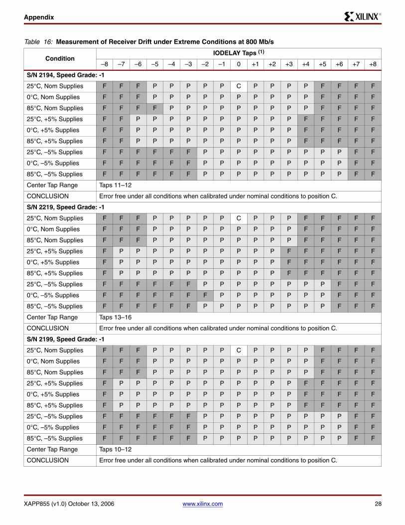
Appendix
XAPP855 (v10) October 13 2006 wwwxilinxcom 29
R
SN 001 Speed Grade -2
25degC Nom Supplies F F F P P P P P C P P P P F F F F
0degC Nom Supplies F F F P P P P P P P P P P F F F F
85degC Nom Supplies F F F P P P P P P P P P P F F F F
25degC +5 Supplies F P P P P P P P P P P P F F F F F
0degC +5 Supplies F P P P P P P P P P P F F F F F F
85degC +5 Supplies F P P P P P P P P P P P F F F F F
25degC ndash5 Supplies F F F F F P P P P P P P P P P F F
0degC ndash5 Supplies F F F F F P P P P P P P P P P F F
85degC ndash5 Supplies F F F F F P P P P P P P P P P F F
Center Tap Range Taps 10ndash12
CONCLUSION Error free under all conditions when calibrated under nominal conditions to position C
SN 002 Speed Grade -2
25degC Nom Supplies F F F P P P P P C P P P P F F F F
0degC Nom Supplies F F F P P P P P P P P P P F F F F
85degC Nom Supplies F F F P P P P P P P P P P F F F F
25degC +5 Supplies F P P P P P P P P P P P F F F F F
0degC +5 Supplies F P P P P P P P P P P P F F F F F
85degC +5 Supplies F F P P P P P P P P P P F F F F F
25degC ndash5 Supplies F F F F F P P P P P P P P P P F F
0degC ndash5 Supplies F F F F F P P P P P P P P P P F F
85degC ndash5 Supplies F F F F F P P P P P P P P P P F F
Center Tap Range Taps 10ndash12
CONCLUSION Error free under all conditions when calibrated under nominal conditions to position C
SN 003 Speed Grade -2
25degC Nom Supplies F F F P P P P P C P P P P F F F F
0degC Nom Supplies F F F P P P P P P P P P P F F F F
85degC Nom Supplies F F F P P P P P P P P P P F F F F
25degC +5 Supplies F P P P P P P P P P P P F F F F F
0degC +5 Supplies F P P P P P P P P P P F F F F F F
85degC +5 Supplies F P P P P P P P P P P P F F F F F
25degC ndash5 Supplies F F F F F F P P P P P P P P P F F
0degC ndash5 Supplies F F F F F F P P P P P P P P P F F
85degC ndash5 Supplies F F F F F F P P P P P P P P P F F
Center Tap Range Taps 11ndash13
CONCLUSION Error free under all conditions when calibrated under nominal conditions to position C
Table 16 Measurement of Receiver Drift under Extreme Conditions at 800 Mbs (Continued)
ConditionIODELAY Taps (1)
ndash8 ndash7 ndash6 ndash5 ndash4 ndash3 ndash2 ndash1 0 +1 +2 +3 +4 +5 +6 +7 +8
Appendix
XAPP855 (v10) October 13 2006 wwwxilinxcom 30
R
SN 004 Speed Grade -3
25degC Nom Supplies F F F P P P P P C P P P P F F F F
0degC Nom Supplies F F F P P P P P P P P P F F F F F
85degC Nom Supplies F F F P P P P P P P P P P F F F F
25degC +5 Supplies F P P P P P P P P P P P F F F F F
0degC +5 Supplies F P P P P P P P P P P P F F F F F
85degC +5 Supplies F F P P P P P P P P P P F F F F F
25degC ndash5 Supplies F F F F F P P P P P P P P P F F F
0degC ndash5 Supplies F F F F F P P P P P P P P P F F F
85degC ndash5 Supplies F F F F F P P P P P P P P P F F F
Center Tap Range Taps 8ndash9 23ndash24
CONCLUSION Error free under all conditions when calibrated under nominal conditions to position C
SN 005 Speed Grade -3
25degC Nom Supplies F F P P P P P P C P P P P F F F F
0degC Nom Supplies F F P P P P P P P P P P P F F F F
85degC Nom Supplies F F F P P P P P P P P P P P F F F
25degC +5 Supplies F P P P P P P P P P P P F F F F F
0degC +5 Supplies F P P P P P P P P P P P F F F F F
85degC +5 Supplies F P P P P P P P P P P P F F F F F
25degC ndash5 Supplies F F F F P P P P P P P P P P P F F
0degC ndash5 Supplies F F F F P P P P P P P P P P P F F
85degC ndash5 Supplies F F F F P P P P P P P P P P P F F
Center Tap Range Taps 9ndash10
CONCLUSION Error free under all conditions when calibrated under nominal conditions to position C
SN 006 Speed Grade -3
25degC Nom Supplies F F P P P P P P C P P P P F F F F
0degC Nom Supplies F F P P P P P P P P P P P F F F F
85degC Nom Supplies F F F P P P P P P P P P P F F F F
25degC +5 Supplies F P P P P P P P P P P P F F F F F
0degC +5 Supplies F P P P P P P P P P P P F F F F F
85degC +5 Supplies F F P P P P P P P P P P F F F F F
25degC ndash5 Supplies F F F P P P P P P P P P P P F F F
0degC ndash5 Supplies F F F P P P P P P P P P P P F F F
85degC ndash5 Supplies F F F F F P P P P P P P P P F F F
Center Tap Range Taps 8ndash9 23ndash24
CONCLUSION Error free under all conditions when calibrated under nominal conditions to position C
Notes 1 IODELAY taps where 0 is the reference tap determined by the bit align machine at nominal voltage and 25degC2 P = Error-free transmission F = Error in transmission C = IODELAY tap position selected by bit-align machine under nominal conditions at 25degC
Table 16 Measurement of Receiver Drift under Extreme Conditions at 800 Mbs (Continued)
ConditionIODELAY Taps (1)
ndash8 ndash7 ndash6 ndash5 ndash4 ndash3 ndash2 ndash1 0 +1 +2 +3 +4 +5 +6 +7 +8
Appendix
XAPP855 (v10) October 13 2006 wwwxilinxcom 31
R
Table 17 Measurement of Receiver Drift under Extreme Conditions at 900 Mbs
ConditionIODELAY Taps (1)
ndash8 ndash7 ndash6 ndash5 ndash4 ndash3 ndash2 ndash1 0 +1 +2 +3 +4 +5 +6 +7 +8
SN 2194 Speed Grade -1
25degC Nom Supplies F F F F F P P P C P P P F F F F F
0degC Nom Supplies F F F F F P P P P P P P F F F F F
85degC Nom Supplies F F F F F P P P P P P P P F F F F
25degC +5 Supplies F F F P P P P P P P P F F F F F F
0degC +5 Supplies F F F P P P P P P P P F F F F F F
85degC +5 Supplies F F F P P P P P P P P F F F F F F
25degC ndash5 Supplies F F F F F F F P P P P P P P F F F
0degC ndash5 Supplies F F F F F F F P P P P P P P F F F
85degC ndash5 Supplies F F F F F F F P P P P P P P F F F
Center Tap Range Taps 11ndash12
CONCLUSION Error free under all conditions when calibrated under nominal conditions to position C
SN 2219 Speed Grade -1
25degC Nom Supplies F F F F F P P P C P P P F F F F F
0degC Nom Supplies F F F F F P P P P P P P F F F F F
85degC Nom Supplies F F F F F P P P P P P P F F F F F
25degC +5 Supplies F F F P P P P P P P F F F F F F F
0degC +5 Supplies F F F P P P P P P P F F F F F F F
85degC +5 Supplies F F F P P P P P P P F F F F F F F
25degC ndash5 Supplies F F F F F F F F F P P P P P F F F
0degC ndash5 Supplies F F F F F F F F F P P P P P F F F
85degC ndash5 Supplies F F F F F F F F P P P P P P F F F
Center Tap Range Taps 12ndash15
CONCLUSION Errors caused by ndash5 variation in supply voltage
SN 2199 Speed Grade -1
25degC Nom Supplies F F F F F P P P C P P P F F F F F
0degC Nom Supplies F F F F F P P P P P P P F F F F F
85degC Nom Supplies F F F F F P P P P P P P F F F F F
25degC +5 Supplies F F F P P P P P P P P F F F F F F
0degC +5 Supplies F F F P P P P P P P P F F F F F F
85degC +5 Supplies F F F P P P P P P P P F F F F F F
25degC ndash5 Supplies F F F F F F F F P P P P P P F F F
0degC ndash5 Supplies F F F F F F F F P P P P P P F F F
85degC ndash5 Supplies F F F F F F F F P P P P P P F F F
Center Tap Range Taps 10ndash12
CONCLUSION Error free under all conditions when calibrated under nominal conditions to position C
Appendix
XAPP855 (v10) October 13 2006 wwwxilinxcom 32
R
SN 001 Speed Grade -2
25degC Nom Supplies F F F F P P P P C P P P P F F F F
0degC Nom Supplies F F F F P P P P P P P P P F F F F
85degC Nom Supplies F F F F F P P P P P P P P F F F F
25degC +5 Supplies F F P P P P P P P P P F F F F F F
0degC +5 Supplies F F P P P P P P P P P F F F F F F
85degC +5 Supplies F F F P P P P P P P P P F F F F F
25degC ndash5 Supplies F F F F F F F P P P P P P P F F F
0degC ndash5 Supplies F F F F F F F P P P P P P P F F F
85degC ndash5 Supplies F F F F F F F P P P P P P P F F F
Center Tap Range Taps 9ndash11
CONCLUSION Error free under all conditions when calibrated under nominal conditions to position C
SN 002 Speed Grade -2
25degC Nom Supplies F F F F P P P P C P P P P F F F F
0degC Nom Supplies F F F F P P P P P P P P F F F F F
85degC Nom Supplies F F F F F P P P P P P P P F F F F
25degC +5 Supplies F F F P P P P P P P P F F F F F F
0degC +5 Supplies F F F P P P P P P P P F F F F F F
85degC +5 Supplies F F F P P P P P P P P P F F F F F
25degC ndash5 Supplies F F F F F F F P P P P P P P F F F
0degC ndash5 Supplies F F F F F F F P P P P P P P F F F
85degC ndash5 Supplies F F F F F F F P P P P P P P F F F
Center Tap Range Taps 10ndash12
CONCLUSION Error free under all conditions when calibrated under nominal conditions to position C
SN 003 Speed Grade -2
25degC Nom Supplies F F F F F P P P C P P P P F F F F
0degC Nom Supplies F F F F F P P P P P P P P F F F F
85degC Nom Supplies F F F F F P P P P P P P P F F F F
25degC +5 Supplies F F P P P P P P P P P F F F F F F
0degC +5 Supplies F F P P P P P P P P P F F F F F F
85degC +5 Supplies F F F P P P P P P P P F F F F F F
25degC ndash5 Supplies F F F F F F F P P P P P P P F F F
0degC ndash5 Supplies F F F F F F F F P P P P P P F F F
85degC ndash5 Supplies F F F F F F F P P P P P P P F F F
Center Tap Range Taps 11ndash13
CONCLUSION Error free under all conditions when calibrated under nominal conditions to position C
Table 17 Measurement of Receiver Drift under Extreme Conditions at 900 Mbs (Continued)
ConditionIODELAY Taps (1)
ndash8 ndash7 ndash6 ndash5 ndash4 ndash3 ndash2 ndash1 0 +1 +2 +3 +4 +5 +6 +7 +8
Appendix
XAPP855 (v10) October 13 2006 wwwxilinxcom 33
R
SN 004 Speed Grade -3
25degC Nom Supplies F F F F P P P P C P P P P F F F F
0degC Nom Supplies F F F P P P P P P P P P P F F F F
85degC Nom Supplies F F F F P P P P P P P P P F F F F
25degC +5 Supplies F F F P P P P P P P P P F F F F F
0degC +5 Supplies F F F P P P P P P P P P F F F F F
85degC +5 Supplies F F F P P P P P P P P P F F F F F
25degC ndash5 Supplies F F F F F F P P P P P P P P F F F
0degC ndash5 Supplies F F F F F F P P P P P P P P F F F
85degC ndash5 Supplies F F F F F F P P P P P P P P F F F
Center Tap Range Taps 7ndash8
CONCLUSION Error free under all conditions when calibrated under nominal conditions to position C
SN 005 Speed Grade ndash3
25degC Nom Supplies F F F P P P P P C P P P P F F F F
0degC Nom Supplies F F F P P P P P P P P P P F F F F
85degC Nom Supplies F F F F P P P P P P P P P F F F F
25degC +5 Supplies F F P P P P P P P P P P F F F F F
0degC +5 Supplies F F P P P P P P P P P P F F F F F
85degC +5 Supplies F F F P P P P P P P P P F F F F F
25degC ndash5 Supplies F F F F F F P P P P P P P P F F F
0degC ndash5 Supplies F F F F F P P P P P P P P P F F F
85degC ndash5 Supplies F F F F F F P P P P P P P P F F F
Center Tap Range Taps 9ndash10
CONCLUSION Error free under all conditions when calibrated under nominal conditions to position C
SN 006 Speed Grade -3
25degC Nom Supplies F F F F P P P P C P P P P F F F F
0degC Nom Supplies F F F F P P P P P P P P P F F F F
85degC Nom Supplies F F F F P P P P P P P P P F F F F
25degC +5 Supplies F F P P P P P P P P P P F F F F F
0degC +5 Supplies F F P P P P P P P P P P F F F F F
85degC +5 Supplies F F F P P P P P P P P P F F F F F
25degC ndash5 Supplies F F F F F P P P P P P P P P F F F
0degC ndash5 Supplies F F F F F P P P P P P P P P F F F
85degC ndash5 Supplies F F F F F F P P P P P P P P F F F
Center Tap Range Taps 7ndash8
CONCLUSION Error free under all conditions when calibrated under nominal conditions to position C
Notes 1 IODELAY taps where 0 is the reference tap determined by the bit align machine at nominal voltage and 25degC2 P = Error-free transmission F = Error in transmission C = IODELAY tap position selected by bit-align machine under nominal conditions at 25degC
Table 17 Measurement of Receiver Drift under Extreme Conditions at 900 Mbs (Continued)
ConditionIODELAY Taps (1)
ndash8 ndash7 ndash6 ndash5 ndash4 ndash3 ndash2 ndash1 0 +1 +2 +3 +4 +5 +6 +7 +8
Appendix
XAPP855 (v10) October 13 2006 wwwxilinxcom 34
R
Table 18 Measurement of Receiver Drift under Extreme Conditions at 1000 Mbs
ConditionIODELAY Taps (1)
ndash8 ndash7 ndash6 ndash5 ndash4 ndash3 ndash2 ndash1 0 +1 +2 +3 +4 +5 +6 +7 +8
SN 2194 Speed Grade -1
25degC Nom Supplies F F F F F P P P C P P F F F F F F
0degC Nom Supplies F F F F F P P P P P P F F F F F F
85degC Nom Supplies F F F F F P P P P P P F F F F F F
25degC +5 Supplies F F F P P P P P P P F F F F F F F
0degC +5 Supplies F F F P P P P P P P F F F F F F F
85degC +5 Supplies F F F F P P P P P P F F F F F F F
25degC ndash5 Supplies F F F F F F F F P P P P P F F F F
0degC ndash5 Supplies F F F F F F F F P P P P P F F F F
85degC ndash5 Supplies F F F F F F F F P P P P P F F F F
Center Tap Range Taps 12ndash13
CONCLUSION Error free under all conditions when calibrated under nominal conditions to position C
SN 2219 Speed Grade -1
25degC Nom Supplies F F F F F F P P C P P F F F F F F
0degC Nom Supplies F F F F F F P P P P P F F F F F F
85degC Nom Supplies F F F F F F P P P P P F F F F F F
25degC +5 Supplies F F F P P P P P P F F F F F F F F
0degC +5 Supplies F F F P P P P P P F F F F F F F F
85degC +5 Supplies F F F F P P P P P F F F F F F F F
25degC ndash5 Supplies F F F F F F F F F P P P P F F F F
0degC ndash5 Supplies F F F F F F F F F F P P P F F F F
85degC ndash5 Supplies F F F F F F F F F P P P P F F F F
Center Tap Range Taps 14ndash17
CONCLUSION Errors caused by ndash5 variation in supply voltage
SN 2199 Speed Grade -1
25degC Nom Supplies F F F F F F P P C P P F F F F F F
0degC Nom Supplies F F F F F F P P P P P F F F F F F
85degC Nom Supplies F F F F F F P P P P P F F F F F F
25degC +5 Supplies F F F F P P P P P P F F F F F F F
0degC +5 Supplies F F F F P P P P P P F F F F F F F
85degC +5 Supplies F F F F P P P P P P F F F F F F F
25degC ndash5 Supplies F F F F F F F F F P P P P F F F F
0degC ndash5 Supplies F F F F F F F F F P P P P F F F F
85degC ndash5 Supplies F F F F F F F F F P P P P F F F F
Center Tap Range Taps 12ndash14
CONCLUSION Errors caused by ndash5 variation in supply voltage
Appendix
XAPP855 (v10) October 13 2006 wwwxilinxcom 35
R
SN 001 Speed Grade -2
25degC Nom Supplies F F F F F F P P C P P P F F F F F
0degC Nom Supplies F F F F F F P P P P P P F F F F F
85degC Nom Supplies F F F F F F P P P P P P F F F F F
25degC +5 Supplies F F F F P P P P P P F F F F F F F
0degC +5 Supplies F F F F P P P P P P F F F F F F F
85degC +5 Supplies F F F F P P P P P P P F F F F F F
25degC ndash5 Supplies F F F F F F F F F P P P P F F F F
0degC ndash5 Supplies F F F F F F F F F P P P P F F F F
85degC ndash5 Supplies F F F F F F F F F P P P P F F F F
Center Tap Range Taps 11ndash12
CONCLUSION Errors caused by ndash5 variation in supply voltage
SN 002 Speed Grade -2
25degC Nom Supplies F F F F F P P P C P P F F F F F F
0degC Nom Supplies F F F F F P P P P P P P F F F F F
85degC Nom Supplies F F F F F P P P P P P P F F F F F
25degC +5 Supplies F F F F P P P P P P F F F F F F F
0degC +5 Supplies F F F P P P P P P P F F F F F F F
85degC +5 Supplies F F F F P P P P P P P F F F F F F
25degC ndash5 Supplies F F F F F F F P P P P P P F F F F
0degC ndash5 Supplies F F F F F F F P P P P P P F F F F
85degC ndash5 Supplies F F F F F F F P P P P P P F F F F
Center Tap Range Taps 11ndash13
CONCLUSION Error free under all conditions when calibrated under nominal conditions to position C
SN 003 Speed Grade -2
25degC Nom Supplies F F F F F F P P C P P F F F F F F
0degC Nom Supplies F F F F F F P P P P P F F F F F F
85degC Nom Supplies F F F F F F P P P P P F F F F F F
25degC +5 Supplies F F F F P P P P P P F F F F F F F
0degC +5 Supplies F F F F P P P P P P F F F F F F F
85degC +5 Supplies F F F F P P P P P P F F F F F F F
25degC ndash5 Supplies F F F F F F F F F P P P P F F F F
0degC ndash5 Supplies F F F F F F F F F P P P P F F F F
85degC ndash5 Supplies F F F F F F F F F P P P P F F F F
Center Tap Range Taps 13ndash14
CONCLUSION Errors caused by ndash5 variation in supply voltage
Table 18 Measurement of Receiver Drift under Extreme Conditions at 1000 Mbs (Continued)
ConditionIODELAY Taps (1)
ndash8 ndash7 ndash6 ndash5 ndash4 ndash3 ndash2 ndash1 0 +1 +2 +3 +4 +5 +6 +7 +8
Appendix
XAPP855 (v10) October 13 2006 wwwxilinxcom 36
R
SN 004 Speed Grade -3
25degC Nom Supplies F F F F F P P P C P P P F F F F F
0degC Nom Supplies F F F F F P P P P P P P F F F F F
85degC Nom Supplies F F F F F P P P P P P P F F F F F
25degC +5 Supplies F F F P P P P P P P P F F F F F F
0degC +5 Supplies F F F P P P P P P P P F F F F F F
85degC +5 Supplies F F F F P P P P P P P P F F F F F
25degC ndash5 Supplies F F F F F F F P P P P P P F F F F
0degC ndash5 Supplies F F F F F F F P P P P P P F F F F
85degC ndash5 Supplies F F F F F F F P P P P P P P F F F
Center Tap Range Taps 9ndash10
CONCLUSION Error free under all conditions when calibrated under nominal conditions to position C
SN 005 Speed Grade -3
25degC Nom Supplies F F F F P P P P C P P P F F F F F
0degC Nom Supplies F F F F P P P P P P P P F F F F F
85degC Nom Supplies F F F F P P P P P P P P F F F F F
25degC +5 Supplies F F F P P P P P P P P F F F F F F
0degC +5 Supplies F F P P P P P P P P P F F F F F F
85degC +5 Supplies F F F P P P P P P P P F F F F F F
25degC ndash5 Supplies F F F F F F P P P P P P P P F F F
0degC ndash5 Supplies F F F F F F P P P P P P P P F F F
85degC ndash5 Supplies F F F F F F P P P P P P P F F F F
Center Tap Range Taps 11ndash12
CONCLUSION Error free under all conditions when calibrated under nominal conditions to position C
SN 006 Speed Grade -3
25degC Nom Supplies F F F F P P P P C P P P F F F F F
0degC Nom Supplies F F F F P P P P P P P P F F F F F
85degC Nom Supplies F F F F P P P P P P P P F F F F F
25degC +5 Supplies F F F P P P P P P P P F F F F F F
0degC +5 Supplies F F F P P P P P P P P F F F F F F
85degC +5 Supplies F F F P P P P P P P P F F F F F F
25degC ndash5 Supplies F F F F F F P P P P P P P F F F F
0degC ndash5 Supplies F F F F F F P P P P P P P F F F F
85degC ndash5 Supplies F F F F F F P P P P P P P F F F F
Center Tap Range Taps 9ndash10
CONCLUSION Error free under all conditions when calibrated under nominal conditions to position C
Notes 1 IODELAY taps where 0 is the reference tap determined by the bit align machine at nominal voltage and 25degC2 P = Error-free transmission F = Error in transmission C = IODELAY tap position selected by bit-align machine under nominal conditions at 25degC
Table 18 Measurement of Receiver Drift under Extreme Conditions at 1000 Mbs (Continued)
ConditionIODELAY Taps (1)
ndash8 ndash7 ndash6 ndash5 ndash4 ndash3 ndash2 ndash1 0 +1 +2 +3 +4 +5 +6 +7 +8
Appendix
XAPP855 (v10) October 13 2006 wwwxilinxcom 37
R
Table 19 Measurement of Receiver Drift under Extreme Conditions at 1100 Mbs
ConditionIODELAY Taps (1)
ndash8 ndash7 ndash6 ndash5 ndash4 ndash3 ndash2 ndash1 0 +1 +2 +3 +4 +5 +6 +7 +8
SN 2194 Speed Grade -1
25degC Nom Supplies F F F F F F P P C P P F F F F F F
0degC Nom Supplies F F F F F F P P P P P F F F F F F
85degC Nom Supplies F F F F F F P P P P P F F F F F F
25degC +5 Supplies F F F F P P P P P F F F F F F F F
0degC +5 Supplies F F F F P P P P P F F F F F F F F
85degC +5 Supplies F F F F P P P P P F F F F F F F F
25degC ndash5 Supplies F F F F F F F F F P P P F F F F F
0degC ndash5 Supplies F F F F F F F F F P P P F F F F F
85degC ndash5 Supplies F F F F F F F F F P P P F F F F F
Center Tap Range Taps 13ndash14
CONCLUSION Errors caused by ndash5 variation in supply voltage
SN 2219 Speed Grade -1
25degC Nom Supplies F F F F F F P P C P F F F F F F F
0degC Nom Supplies F F F F F F P P P P F F F F F F F
85degC Nom Supplies F F F F F F P P P P F F F F F F F
25degC +5 Supplies F F F F P P P P F F F F F F F F F
0degC +5 Supplies F F F F P P P P F F F F F F F F F
85degC +5 Supplies F F F F P P P P F F F F F F F F F
25degC ndash5 Supplies F F F F F F F F F F P P F F F F F
0degC ndash5 Supplies F F F F F F F F F F P P F F F F F
85degC ndash5 Supplies F F F F F F F F F P P P F F F F F
Center Tap Range Taps 6 15ndash17
CONCLUSION Errors caused by plusmn5 variation in supply voltage
SN 2199 Speed Grade -1
25degC Nom Supplies F F F F F F F P C P F F F F F F F
0degC Nom Supplies F F F F F F F P P P F F F F F F F
85degC Nom Supplies F F F F F F F P P P F F F F F F F
25degC +5 Supplies F F F F P P P P P F F F F F F F F
0degC +5 Supplies F F F F P P P P P F F F F F F F F
85degC +5 Supplies F F F F F P P P P F F F F F F F F
25degC ndash5 Supplies F F F F F F F F F F P P F F F F F
0degC ndash5 Supplies F F F F F F F F F F P P F F F F F
85degC ndash5 Supplies F F F F F F F F F F P P F F F F F
Center Tap Range Taps 13ndash15
CONCLUSION Errors caused by ndash5 variation in supply voltage
Appendix
XAPP855 (v10) October 13 2006 wwwxilinxcom 38
R
SN 001 Speed Grade -2
25degC Nom Supplies F F F F F F P P C P P F F F F F F
0degC Nom Supplies F F F F F F P P P P P F F F F F F
85degC Nom Supplies F F F F F F P P P P P F F F F F F
25degC +5 Supplies F F F F P P P P P F F F F F F F F
0degC +5 Supplies F F F F P P P P P F F F F F F F F
85degC +5 Supplies F F F F P P P P P F F F F F F F F
25degC ndash5 Supplies F F F F F F F F P P P P F F F F F
0degC ndash5 Supplies F F F F F F F F P P P P F F F F F
85degC ndash5 Supplies F F F F F F F F P P P P F F F F F
Center Tap Range Taps 12ndash13
CONCLUSION Error free under all conditions when calibrated under nominal conditions to position C
SN 002 Speed Grade -2
25degC Nom Supplies F F F F F P P P C P F F F F F F F
0degC Nom Supplies F F F F F P P P P P F F F F F F F
85degC Nom Supplies F F F F F F P P P P F F F F F F F
25degC +5 Supplies F F F F P P P P P F F F F F F F F
0degC +5 Supplies F F F P P P P P P F F F F F F F F
85degC +5 Supplies F F F F P P P P P F F F F F F F F
25degC ndash5 Supplies F F F F F F F F P P P P F F F F F
0degC ndash5 Supplies F F F F F F F F P P P P F F F F F
85degC ndash5 Supplies F F F F F F F F P P P P F F F F F
Center Tap Range Taps 13ndash14
CONCLUSION Error free under all conditions when calibrated under nominal conditions to position C
SN 003 Speed Grade -2
25degC Nom Supplies F F F F F F F P C P F F F F F F F
0degC Nom Supplies F F F F F F F P P P F F F F F F F
85degC Nom Supplies F F F F F F F P P P P F F F F F F
25degC +5 Supplies F F F F F P P P P F F F F F F F F
0degC +5 Supplies F F F F F P P P P F F F F F F F F
85degC +5 Supplies F F F F F P P P P F F F F F F F F
25degC ndash5 Supplies F F F F F F F F F F P P F F F F F
0degC ndash5 Supplies F F F F F F F F F F P P F F F F F
85degC ndash5 Supplies F F F F F F F F F P P P F F F F F
Center Tap Range Taps 14ndash16
CONCLUSION Errors caused by ndash5 variation in supply voltage
Table 19 Measurement of Receiver Drift under Extreme Conditions at 1100 Mbs (Continued)
ConditionIODELAY Taps (1)
ndash8 ndash7 ndash6 ndash5 ndash4 ndash3 ndash2 ndash1 0 +1 +2 +3 +4 +5 +6 +7 +8
Appendix
XAPP855 (v10) October 13 2006 wwwxilinxcom 39
R
SN 004 Speed Grade -3
25degC Nom Supplies F F F F F P P P C P P F F F F F F
0degC Nom Supplies F F F F F P P P P P P F F F F F F
85degC Nom Supplies F F F F F F P P P P P F F F F F F
25degC +5 Supplies F F F F P P P P P P F F F F F F F
0degC +5 Supplies F F F F P P P P P P F F F F F F F
85degC +5 Supplies F F F F P P P P P P F F F F F F F
25degC ndash5 Supplies F F F F F F F F P P P P F F F F F
0degC ndash5 Supplies F F F F F F F P P P P P F F F F F
85degC ndash5 Supplies F F F F F F F F P P P P P F F F F
Center Tap Range Taps 9ndash10
CONCLUSION Error free under all conditions when calibrated under nominal conditions to position C
SN 005 Speed Grade -3
25degC Nom Supplies F F F F F P P P C P P F F F F F F
0degC Nom Supplies F F F F F P P P P P P F F F F F F
85degC Nom Supplies F F F F F F P P P P P F F F F F F
25degC +5 Supplies F F F F P P P P P P F F F F F F F
0degC +5 Supplies F F F F P P P P P P F F F F F F F
85degC +5 Supplies F F F F P P P P P P F F F F F F F
25degC ndash5 Supplies F F F F F F F P P P P P P F F F F
0degC ndash5 Supplies F F F F F F F P P P P P P F F F F
85degC ndash5 Supplies F F F F F F F P P P P P P F F F F
Center Tap Range Taps 11ndash12
CONCLUSION Error free under all conditions when calibrated under nominal conditions to position C
SN 006 Speed Grade -3
25degC Nom Supplies F F F F F P P P C P P P F F F F F
0degC Nom Supplies F F F F F P P P P P P F F F F F F
85degC Nom Supplies F F F F F P P P P P P P F F F F F
25degC +5 Supplies F F F F P P P P P P P F F F F F F
0degC +5 Supplies F F F P P P P P P P F F F F F F F
85degC +5 Supplies F F F F P P P P P P P F F F F F F
25degC ndash5 Supplies F F F F F F P P P P P P P F F F F
0degC ndash5 Supplies F F F F F F P P P P P P P F F F F
85degC ndash5 Supplies F F F F F F F P P P P P P F F F F
Center Tap Range Taps 9ndash10
CONCLUSION Error free under all conditions when calibrated under nominal conditions to position C
Notes 1 IODELAY taps where 0 is the reference tap determined by the bit align machine at nominal voltage and 25degC2 P = Error-free transmission F = Error in transmission C = IODELAY tap position selected by bit-align machine under nominal conditions at 25degC
Table 19 Measurement of Receiver Drift under Extreme Conditions at 1100 Mbs (Continued)
ConditionIODELAY Taps (1)
ndash8 ndash7 ndash6 ndash5 ndash4 ndash3 ndash2 ndash1 0 +1 +2 +3 +4 +5 +6 +7 +8
Appendix
XAPP855 (v10) October 13 2006 wwwxilinxcom 40
R
Table 20 Measurement of Receiver Drift under Extreme Conditions at 1200 Mbs
ConditionIODELAY Taps (1)
ndash8 ndash7 ndash6 ndash5 ndash4 ndash3 ndash2 ndash1 0 +1 +2 +3 +4 +5 +6 +7 +8
SN 2194 Speed Grade -1
25degC Nom Supplies F F F F F F F P C F F F F F F F F
0degC Nom Supplies F F F F F F F P P F F F F F F F F
85degC Nom Supplies F F F F F F F P P F F F F F F F F
25degC +5 Supplies F F F F P P P P F F F F F F F F F
0degC +5 Supplies F F F F P P P P F F F F F F F F F
85degC +5 Supplies F F F F F P P P F F F F F F F F F
25degC ndash5 Supplies F F F F F F F F F P P F F F F F F
0degC ndash5 Supplies F F F F F F F F F F P F F F F F F
85degC ndash5 Supplies F F F F F F F F F P F F F F F F F
Center Tap Range Taps 13ndash15
CONCLUSION Errors caused by plusmn5 variation in supply voltage
SN 2219 Speed Grade -1
25degC Nom Supplies F F F F F F F F C F F F F F F F F
0degC Nom Supplies F F F F F F F P P F F F F F F F F
85degC Nom Supplies F F F F F F F F P F F F F F F F F
25degC +5 Supplies F F F F F P P P F F F F F F F F F
0degC +5 Supplies F F F F F P P P F F F F F F F F F
85degC +5 Supplies F F F F F F P P F F F F F F F F F
25degC ndash5 Supplies F F F F F F F F F F F F F F F F F
0degC ndash5 Supplies F F F F F F F F F F F F F F F F F
85degC ndash5 Supplies F F F F F F F F F F F F F F F F F
Center Tap Range Taps 6ndash7 16ndash17
CONCLUSION Errors caused by plusmn5 variation in supply voltage
SN 2199 Speed Grade -1
25degC Nom Supplies F F F F F F F P C F F F F F F F F
0degC Nom Supplies F F F F F F F P P F F F F F F F F
85degC Nom Supplies F F F F F F F F P F F F F F F F F
25degC +5 Supplies F F F F F P P P F F F F F F F F F
0degC +5 Supplies F F F F F P P P F F F F F F F F F
85degC +5 Supplies F F F F F P P P F F F F F F F F F
25degC ndash5 Supplies F F F F F F F F F F F F F F F F F
0degC ndash5 Supplies F F F F F F F F F F F F F F F F F
85degC ndash5 Supplies F F F F F F F F F F F F F F F F F
Center Tap Range Taps 13ndash15
CONCLUSION Errors caused by plusmn5 variation in supply voltage
Appendix
XAPP855 (v10) October 13 2006 wwwxilinxcom 41
R
SN 001 Speed Grade -2
25degC Nom Supplies F F F F F F F P C P F F F F F F F
0degC Nom Supplies F F F F F F F P P P F F F F F F F
85degC Nom Supplies F F F F F F F P P P F F F F F F F
25degC +5 Supplies F F F F F P P P P F F F F F F F F
0degC +5 Supplies F F F F P P P P P F F F F F F F F
85degC +5 Supplies F F F F F P P P P F F F F F F F F
25degC ndash5 Supplies F F F F F F F F F F P F F F F F F
0degC ndash5 Supplies F F F F F F F F F F P F F F F F F
85degC ndash5 Supplies F F F F F F F F F F P F F F F F F
Center Tap Range Taps 12ndash13
CONCLUSION Errors caused by ndash5 variation in supply voltage
SN 002 Speed Grade -2
25degC Nom Supplies F F F F F F P P C P F F F F F F F
0degC Nom Supplies F F F F F F P P P P F F F F F F F
85degC Nom Supplies F F F F F F F P P P F F F F F F F
25degC +5 Supplies F F F F P P P P F F F F F F F F F
0degC +5 Supplies F F F F P P P P F F F F F F F F F
85degC +5 Supplies F F F F F P P P F F F F F F F F F
25degC ndash5 Supplies F F F F F F F F P P P F F F F F F
0degC ndash5 Supplies F F F F F F F F P P P F F F F F F
85degC ndash5 Supplies F F F F F F F F F P P F F F F F F
Center Tap Range Taps 13ndash14
CONCLUSION Errors caused by plusmn5 variation in supply voltage
SN 003 Speed Grade -2
25degC Nom Supplies F F F F F F F P C F F F F F F F F
0degC Nom Supplies F F F F F F F P P F F F F F F F F
85degC Nom Supplies F F F F F F F F P F F F F F F F F
25degC +5 Supplies F F F F F P P P F F F F F F F F F
0degC +5 Supplies F F F F F P P P F F F F F F F F F
85degC +5 Supplies F F F F F F P P F F F F F F F F F
25degC ndash5 Supplies F F F F F F F F F F F F F F F F F
0degC ndash5 Supplies F F F F F F F F F F F F F F F F F
85degC ndash5 Supplies F F F F F F F F F F F F F F F F F
Center Tap Range Taps 14ndash15
CONCLUSION Errors caused by plusmn5 variation in supply voltage
Table 20 Measurement of Receiver Drift under Extreme Conditions at 1200 Mbs (Continued)
ConditionIODELAY Taps (1)
ndash8 ndash7 ndash6 ndash5 ndash4 ndash3 ndash2 ndash1 0 +1 +2 +3 +4 +5 +6 +7 +8
Appendix
XAPP855 (v10) October 13 2006 wwwxilinxcom 42
R
SN 004 Speed Grade -3
25degC Nom Supplies F F F F F F P P C P F F F F F F F
0degC Nom Supplies F F F F F P P P P P F F F F F F F
85degC Nom Supplies F F F F F F P P P P F F F F F F F
25degC +5 Supplies F F F F P P P P P F F F F F F F F
0degC +5 Supplies F F F F P P P P P F F F F F F F F
85degC +5 Supplies F F F F F P P P P F F F F F F F F
25degC ndash5 Supplies F F F F F F F F P P P F F F F F F
0degC ndash5 Supplies F F F F F F F F P P P F F F F F F
85degC ndash5 Supplies F F F F F F F F P P P F F F F F F
Center Tap Range Taps 9ndash11
CONCLUSION Error free under all conditions when calibrated under nominal conditions to position C
SN 005 Speed Grade -3
25degC Nom Supplies F F F F F P P P C P F F F F F F F
0degC Nom Supplies F F F F F P P P P P F F F F F F F
85degC Nom Supplies F F F F F F P P P P F F F F F F F
25degC +5 Supplies F F F F P P P P P F F F F F F F F
0degC +5 Supplies F F F P P P P P P F F F F F F F F
85degC +5 Supplies F F F F P P P P P F F F F F F F F
25degC ndash5 Supplies F F F F F F F P P P P P F F F F F
0degC ndash5 Supplies F F F F F F F P P P P P F F F F F
85degC ndash5 Supplies F F F F F F F F P P P F F F F F F
Center Tap Range Taps 11ndash13
CONCLUSION Error free under all conditions when calibrated under nominal conditions to position C
SN 006 Speed Grade -3
25degC Nom Supplies F F F F F P P P C P F F F F F F F
0degC Nom Supplies F F F F F P P P P P F F F F F F F
85degC Nom Supplies F F F F F P P P P P F F F F F F F
25degC +5 Supplies F F F P P P P P P F F F F F F F F
0degC +5 Supplies F F F P P P P P P F F F F F F F F
85degC +5 Supplies F F F F P P P P P F F F F F F F F
25degC ndash5 Supplies F F F F F F F P P P P F F F F F F
0degC ndash5 Supplies F F F F F F P P P P P F F F F F F
85degC ndash5 Supplies F F F F F F F P P P P F F F F F F
Center Tap Range Taps 10ndash11
CONCLUSION Error free under all conditions when calibrated under nominal conditions to position C
Notes 1 IODELAY taps where 0 is the reference tap determined by the bit align machine at nominal voltage and 25degC2 P = Error-free transmission F = Error in transmission C = IODELAY tap position selected by bit-align machine under nominal conditions at 25degC
Table 20 Measurement of Receiver Drift under Extreme Conditions at 1200 Mbs (Continued)
ConditionIODELAY Taps (1)
ndash8 ndash7 ndash6 ndash5 ndash4 ndash3 ndash2 ndash1 0 +1 +2 +3 +4 +5 +6 +7 +8
Revision History
XAPP855 (v10) October 13 2006 wwwxilinxcom 43
R
Revision History
The following table shows the revision history for this document
Date Version Revision
101306 10 Initial Xilinx release
- 16-Channel DDR LVDS Interface with Per-Channel Alignment
-
- Summary
- Introduction
-
- Figure 1 Full-Duplex 16-Channel DDR Link between a Virtex-5 Device and Another Device with a 16-Channel DDR Interface
- Figure 2 BERT Testbench for Hardware Verification of the DDR Interface
- Figure 3 Design Hierarchy of the Interface (TX and RX)
-
- DDR Transmitter
-
- Table 1 DDR_8TO1_16CHAN_TX Module Port Definitions
- Figure 4 MasterSlave OSERDES Pair for a Single Data Channel with 81 Serialization
- Figure 5 Block Diagram of TX Interface
- Table 2 DDR TX Interface Utilization Statistics
-
- Interface Clocking
-
- Figure 6 Global and Regional Clocking Schemes in Virtex-5 FPGAs
- Table 3 Comparison of Global and IO Clock Performance by Speed Grade
-
- DDR Receiver
-
- Table 4 DDR_8TO1_16CHAN_RX Module Port Definitions
- Figure 7 MasterSlave ISERDES Pair for a Single Data Channel with 18 Deserialization
- Figure 8 Block Diagram of RX Interface
- Table 5 DDR RX Interface Utilization Statistics
-
- Receiver Interface Dynamic Timing
-
- Inherent Timing
-
- Figure 9 Timing Components of RX Data and Clock Paths
- Figure 10 ISE Timing Analyzer Properties Used in this Document
- Table 6 Datapath Timing Definitions
- Table 7 Clock Path Timing Definitions
- Table 8 Datapath Delay Inventory for a -1 Speed Grade XC5VLX50T Device
- Table 9 Clock Path Delay Inventory for a -1 Speed Grade XC5VLX50T Device
- Figure 11 Timing Windows Show Uncertainty in ClockData Relationship as Calculated by Timing Analyzer
-
- Dynamic Timing and BIT_ALIGN_MACHINE
-
- Figure 12 Inherent Timing Windows Shown in Relation to Multiple Data Rates
- Figure 13 Dynamic Bit-Alignment Procedure in BIT_ALIGN_MACHINE
- Table 10 Word Alignment in the DDR Receiver
- Figure 14 FSM in the BIT_ALIGN_MACHINE Module
-
- Interface Timing Budget
-
- Interface Characterization
-
- Figure 15 Bit-Alignment Algorithm Performance
- Table 11 Tap Setting Range For Various Data Rates Measured on a -2 Device
- Table 12 Measurement of Receiver Drift under Extreme Conditions for Multiple Data Rates
- Pattern Dependence of Receiver Performance
-
- Table 13 Link Performance for Various Types of Data Measured on a -2 Device
-
- Resetting the Interface
-
- Figure 16 Recommended Interface Reset Timing
-
- Conclusion
-
- Table 14 Performance of 16-Channel DDR Interface
-
- Appendix
-
- Performance Characterization Data
-
- Table 15 Summary of Interface Characterization Results
- Table 16 Measurement of Receiver Drift under Extreme Conditions at 800 Mbs
- Table 17 Measurement of Receiver Drift under Extreme Conditions at 900 Mbs
- Table 18 Measurement of Receiver Drift under Extreme Conditions at 1000 Mbs
- Table 19 Measurement of Receiver Drift under Extreme Conditions at 1100 Mbs
- Table 20 Measurement of Receiver Drift under Extreme Conditions at 1200 Mbs
-
- Revision History
-
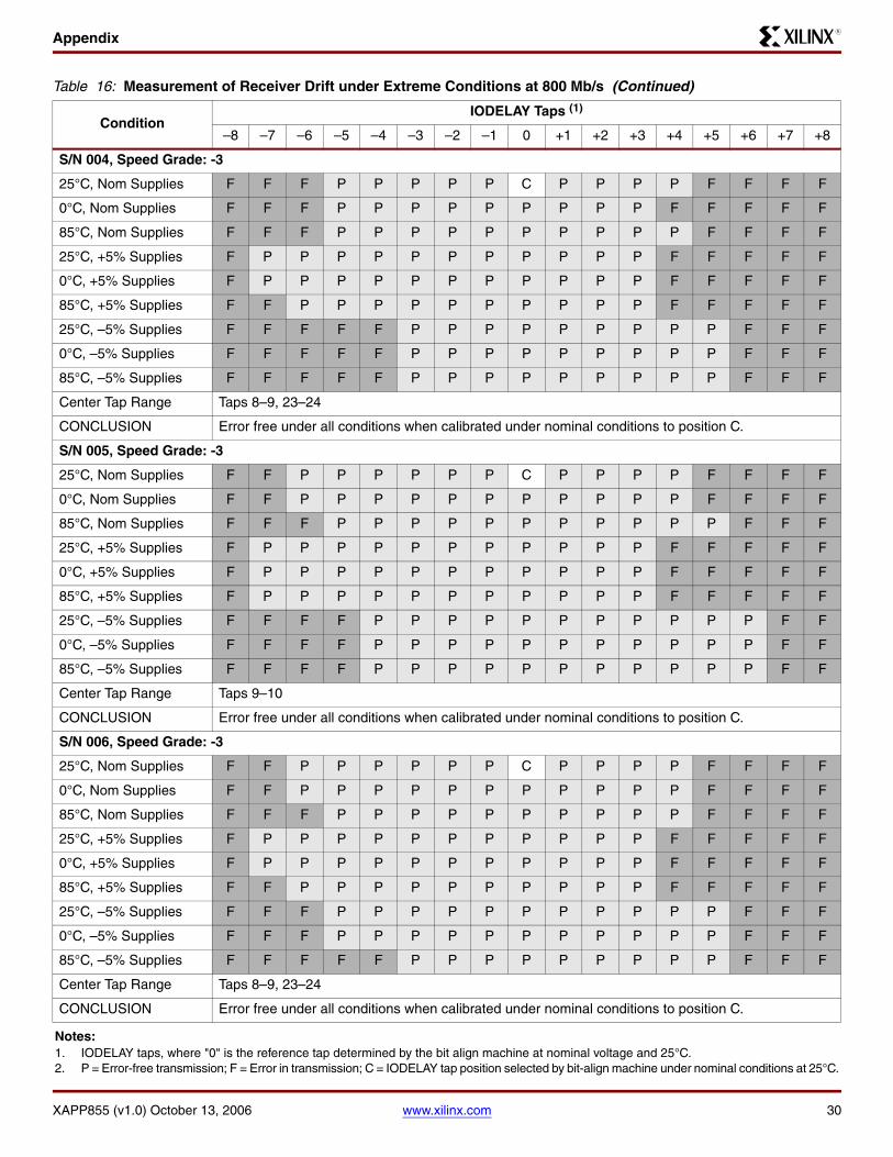
Appendix
XAPP855 (v10) October 13 2006 wwwxilinxcom 31
R
Table 17 Measurement of Receiver Drift under Extreme Conditions at 900 Mbs
ConditionIODELAY Taps (1)
ndash8 ndash7 ndash6 ndash5 ndash4 ndash3 ndash2 ndash1 0 +1 +2 +3 +4 +5 +6 +7 +8
SN 2194 Speed Grade -1
25degC Nom Supplies F F F F F P P P C P P P F F F F F
0degC Nom Supplies F F F F F P P P P P P P F F F F F
85degC Nom Supplies F F F F F P P P P P P P P F F F F
25degC +5 Supplies F F F P P P P P P P P F F F F F F
0degC +5 Supplies F F F P P P P P P P P F F F F F F
85degC +5 Supplies F F F P P P P P P P P F F F F F F
25degC ndash5 Supplies F F F F F F F P P P P P P P F F F
0degC ndash5 Supplies F F F F F F F P P P P P P P F F F
85degC ndash5 Supplies F F F F F F F P P P P P P P F F F
Center Tap Range Taps 11ndash12
CONCLUSION Error free under all conditions when calibrated under nominal conditions to position C
SN 2219 Speed Grade -1
25degC Nom Supplies F F F F F P P P C P P P F F F F F
0degC Nom Supplies F F F F F P P P P P P P F F F F F
85degC Nom Supplies F F F F F P P P P P P P F F F F F
25degC +5 Supplies F F F P P P P P P P F F F F F F F
0degC +5 Supplies F F F P P P P P P P F F F F F F F
85degC +5 Supplies F F F P P P P P P P F F F F F F F
25degC ndash5 Supplies F F F F F F F F F P P P P P F F F
0degC ndash5 Supplies F F F F F F F F F P P P P P F F F
85degC ndash5 Supplies F F F F F F F F P P P P P P F F F
Center Tap Range Taps 12ndash15
CONCLUSION Errors caused by ndash5 variation in supply voltage
SN 2199 Speed Grade -1
25degC Nom Supplies F F F F F P P P C P P P F F F F F
0degC Nom Supplies F F F F F P P P P P P P F F F F F
85degC Nom Supplies F F F F F P P P P P P P F F F F F
25degC +5 Supplies F F F P P P P P P P P F F F F F F
0degC +5 Supplies F F F P P P P P P P P F F F F F F
85degC +5 Supplies F F F P P P P P P P P F F F F F F
25degC ndash5 Supplies F F F F F F F F P P P P P P F F F
0degC ndash5 Supplies F F F F F F F F P P P P P P F F F
85degC ndash5 Supplies F F F F F F F F P P P P P P F F F
Center Tap Range Taps 10ndash12
CONCLUSION Error free under all conditions when calibrated under nominal conditions to position C
Appendix
XAPP855 (v10) October 13 2006 wwwxilinxcom 32
R
SN 001 Speed Grade -2
25degC Nom Supplies F F F F P P P P C P P P P F F F F
0degC Nom Supplies F F F F P P P P P P P P P F F F F
85degC Nom Supplies F F F F F P P P P P P P P F F F F
25degC +5 Supplies F F P P P P P P P P P F F F F F F
0degC +5 Supplies F F P P P P P P P P P F F F F F F
85degC +5 Supplies F F F P P P P P P P P P F F F F F
25degC ndash5 Supplies F F F F F F F P P P P P P P F F F
0degC ndash5 Supplies F F F F F F F P P P P P P P F F F
85degC ndash5 Supplies F F F F F F F P P P P P P P F F F
Center Tap Range Taps 9ndash11
CONCLUSION Error free under all conditions when calibrated under nominal conditions to position C
SN 002 Speed Grade -2
25degC Nom Supplies F F F F P P P P C P P P P F F F F
0degC Nom Supplies F F F F P P P P P P P P F F F F F
85degC Nom Supplies F F F F F P P P P P P P P F F F F
25degC +5 Supplies F F F P P P P P P P P F F F F F F
0degC +5 Supplies F F F P P P P P P P P F F F F F F
85degC +5 Supplies F F F P P P P P P P P P F F F F F
25degC ndash5 Supplies F F F F F F F P P P P P P P F F F
0degC ndash5 Supplies F F F F F F F P P P P P P P F F F
85degC ndash5 Supplies F F F F F F F P P P P P P P F F F
Center Tap Range Taps 10ndash12
CONCLUSION Error free under all conditions when calibrated under nominal conditions to position C
SN 003 Speed Grade -2
25degC Nom Supplies F F F F F P P P C P P P P F F F F
0degC Nom Supplies F F F F F P P P P P P P P F F F F
85degC Nom Supplies F F F F F P P P P P P P P F F F F
25degC +5 Supplies F F P P P P P P P P P F F F F F F
0degC +5 Supplies F F P P P P P P P P P F F F F F F
85degC +5 Supplies F F F P P P P P P P P F F F F F F
25degC ndash5 Supplies F F F F F F F P P P P P P P F F F
0degC ndash5 Supplies F F F F F F F F P P P P P P F F F
85degC ndash5 Supplies F F F F F F F P P P P P P P F F F
Center Tap Range Taps 11ndash13
CONCLUSION Error free under all conditions when calibrated under nominal conditions to position C
Table 17 Measurement of Receiver Drift under Extreme Conditions at 900 Mbs (Continued)
ConditionIODELAY Taps (1)
ndash8 ndash7 ndash6 ndash5 ndash4 ndash3 ndash2 ndash1 0 +1 +2 +3 +4 +5 +6 +7 +8
Appendix
XAPP855 (v10) October 13 2006 wwwxilinxcom 33
R
SN 004 Speed Grade -3
25degC Nom Supplies F F F F P P P P C P P P P F F F F
0degC Nom Supplies F F F P P P P P P P P P P F F F F
85degC Nom Supplies F F F F P P P P P P P P P F F F F
25degC +5 Supplies F F F P P P P P P P P P F F F F F
0degC +5 Supplies F F F P P P P P P P P P F F F F F
85degC +5 Supplies F F F P P P P P P P P P F F F F F
25degC ndash5 Supplies F F F F F F P P P P P P P P F F F
0degC ndash5 Supplies F F F F F F P P P P P P P P F F F
85degC ndash5 Supplies F F F F F F P P P P P P P P F F F
Center Tap Range Taps 7ndash8
CONCLUSION Error free under all conditions when calibrated under nominal conditions to position C
SN 005 Speed Grade ndash3
25degC Nom Supplies F F F P P P P P C P P P P F F F F
0degC Nom Supplies F F F P P P P P P P P P P F F F F
85degC Nom Supplies F F F F P P P P P P P P P F F F F
25degC +5 Supplies F F P P P P P P P P P P F F F F F
0degC +5 Supplies F F P P P P P P P P P P F F F F F
85degC +5 Supplies F F F P P P P P P P P P F F F F F
25degC ndash5 Supplies F F F F F F P P P P P P P P F F F
0degC ndash5 Supplies F F F F F P P P P P P P P P F F F
85degC ndash5 Supplies F F F F F F P P P P P P P P F F F
Center Tap Range Taps 9ndash10
CONCLUSION Error free under all conditions when calibrated under nominal conditions to position C
SN 006 Speed Grade -3
25degC Nom Supplies F F F F P P P P C P P P P F F F F
0degC Nom Supplies F F F F P P P P P P P P P F F F F
85degC Nom Supplies F F F F P P P P P P P P P F F F F
25degC +5 Supplies F F P P P P P P P P P P F F F F F
0degC +5 Supplies F F P P P P P P P P P P F F F F F
85degC +5 Supplies F F F P P P P P P P P P F F F F F
25degC ndash5 Supplies F F F F F P P P P P P P P P F F F
0degC ndash5 Supplies F F F F F P P P P P P P P P F F F
85degC ndash5 Supplies F F F F F F P P P P P P P P F F F
Center Tap Range Taps 7ndash8
CONCLUSION Error free under all conditions when calibrated under nominal conditions to position C
Notes 1 IODELAY taps where 0 is the reference tap determined by the bit align machine at nominal voltage and 25degC2 P = Error-free transmission F = Error in transmission C = IODELAY tap position selected by bit-align machine under nominal conditions at 25degC
Table 17 Measurement of Receiver Drift under Extreme Conditions at 900 Mbs (Continued)
ConditionIODELAY Taps (1)
ndash8 ndash7 ndash6 ndash5 ndash4 ndash3 ndash2 ndash1 0 +1 +2 +3 +4 +5 +6 +7 +8
Appendix
XAPP855 (v10) October 13 2006 wwwxilinxcom 34
R
Table 18 Measurement of Receiver Drift under Extreme Conditions at 1000 Mbs
ConditionIODELAY Taps (1)
ndash8 ndash7 ndash6 ndash5 ndash4 ndash3 ndash2 ndash1 0 +1 +2 +3 +4 +5 +6 +7 +8
SN 2194 Speed Grade -1
25degC Nom Supplies F F F F F P P P C P P F F F F F F
0degC Nom Supplies F F F F F P P P P P P F F F F F F
85degC Nom Supplies F F F F F P P P P P P F F F F F F
25degC +5 Supplies F F F P P P P P P P F F F F F F F
0degC +5 Supplies F F F P P P P P P P F F F F F F F
85degC +5 Supplies F F F F P P P P P P F F F F F F F
25degC ndash5 Supplies F F F F F F F F P P P P P F F F F
0degC ndash5 Supplies F F F F F F F F P P P P P F F F F
85degC ndash5 Supplies F F F F F F F F P P P P P F F F F
Center Tap Range Taps 12ndash13
CONCLUSION Error free under all conditions when calibrated under nominal conditions to position C
SN 2219 Speed Grade -1
25degC Nom Supplies F F F F F F P P C P P F F F F F F
0degC Nom Supplies F F F F F F P P P P P F F F F F F
85degC Nom Supplies F F F F F F P P P P P F F F F F F
25degC +5 Supplies F F F P P P P P P F F F F F F F F
0degC +5 Supplies F F F P P P P P P F F F F F F F F
85degC +5 Supplies F F F F P P P P P F F F F F F F F
25degC ndash5 Supplies F F F F F F F F F P P P P F F F F
0degC ndash5 Supplies F F F F F F F F F F P P P F F F F
85degC ndash5 Supplies F F F F F F F F F P P P P F F F F
Center Tap Range Taps 14ndash17
CONCLUSION Errors caused by ndash5 variation in supply voltage
SN 2199 Speed Grade -1
25degC Nom Supplies F F F F F F P P C P P F F F F F F
0degC Nom Supplies F F F F F F P P P P P F F F F F F
85degC Nom Supplies F F F F F F P P P P P F F F F F F
25degC +5 Supplies F F F F P P P P P P F F F F F F F
0degC +5 Supplies F F F F P P P P P P F F F F F F F
85degC +5 Supplies F F F F P P P P P P F F F F F F F
25degC ndash5 Supplies F F F F F F F F F P P P P F F F F
0degC ndash5 Supplies F F F F F F F F F P P P P F F F F
85degC ndash5 Supplies F F F F F F F F F P P P P F F F F
Center Tap Range Taps 12ndash14
CONCLUSION Errors caused by ndash5 variation in supply voltage
Appendix
XAPP855 (v10) October 13 2006 wwwxilinxcom 35
R
SN 001 Speed Grade -2
25degC Nom Supplies F F F F F F P P C P P P F F F F F
0degC Nom Supplies F F F F F F P P P P P P F F F F F
85degC Nom Supplies F F F F F F P P P P P P F F F F F
25degC +5 Supplies F F F F P P P P P P F F F F F F F
0degC +5 Supplies F F F F P P P P P P F F F F F F F
85degC +5 Supplies F F F F P P P P P P P F F F F F F
25degC ndash5 Supplies F F F F F F F F F P P P P F F F F
0degC ndash5 Supplies F F F F F F F F F P P P P F F F F
85degC ndash5 Supplies F F F F F F F F F P P P P F F F F
Center Tap Range Taps 11ndash12
CONCLUSION Errors caused by ndash5 variation in supply voltage
SN 002 Speed Grade -2
25degC Nom Supplies F F F F F P P P C P P F F F F F F
0degC Nom Supplies F F F F F P P P P P P P F F F F F
85degC Nom Supplies F F F F F P P P P P P P F F F F F
25degC +5 Supplies F F F F P P P P P P F F F F F F F
0degC +5 Supplies F F F P P P P P P P F F F F F F F
85degC +5 Supplies F F F F P P P P P P P F F F F F F
25degC ndash5 Supplies F F F F F F F P P P P P P F F F F
0degC ndash5 Supplies F F F F F F F P P P P P P F F F F
85degC ndash5 Supplies F F F F F F F P P P P P P F F F F
Center Tap Range Taps 11ndash13
CONCLUSION Error free under all conditions when calibrated under nominal conditions to position C
SN 003 Speed Grade -2
25degC Nom Supplies F F F F F F P P C P P F F F F F F
0degC Nom Supplies F F F F F F P P P P P F F F F F F
85degC Nom Supplies F F F F F F P P P P P F F F F F F
25degC +5 Supplies F F F F P P P P P P F F F F F F F
0degC +5 Supplies F F F F P P P P P P F F F F F F F
85degC +5 Supplies F F F F P P P P P P F F F F F F F
25degC ndash5 Supplies F F F F F F F F F P P P P F F F F
0degC ndash5 Supplies F F F F F F F F F P P P P F F F F
85degC ndash5 Supplies F F F F F F F F F P P P P F F F F
Center Tap Range Taps 13ndash14
CONCLUSION Errors caused by ndash5 variation in supply voltage
Table 18 Measurement of Receiver Drift under Extreme Conditions at 1000 Mbs (Continued)
ConditionIODELAY Taps (1)
ndash8 ndash7 ndash6 ndash5 ndash4 ndash3 ndash2 ndash1 0 +1 +2 +3 +4 +5 +6 +7 +8
Appendix
XAPP855 (v10) October 13 2006 wwwxilinxcom 36
R
SN 004 Speed Grade -3
25degC Nom Supplies F F F F F P P P C P P P F F F F F
0degC Nom Supplies F F F F F P P P P P P P F F F F F
85degC Nom Supplies F F F F F P P P P P P P F F F F F
25degC +5 Supplies F F F P P P P P P P P F F F F F F
0degC +5 Supplies F F F P P P P P P P P F F F F F F
85degC +5 Supplies F F F F P P P P P P P P F F F F F
25degC ndash5 Supplies F F F F F F F P P P P P P F F F F
0degC ndash5 Supplies F F F F F F F P P P P P P F F F F
85degC ndash5 Supplies F F F F F F F P P P P P P P F F F
Center Tap Range Taps 9ndash10
CONCLUSION Error free under all conditions when calibrated under nominal conditions to position C
SN 005 Speed Grade -3
25degC Nom Supplies F F F F P P P P C P P P F F F F F
0degC Nom Supplies F F F F P P P P P P P P F F F F F
85degC Nom Supplies F F F F P P P P P P P P F F F F F
25degC +5 Supplies F F F P P P P P P P P F F F F F F
0degC +5 Supplies F F P P P P P P P P P F F F F F F
85degC +5 Supplies F F F P P P P P P P P F F F F F F
25degC ndash5 Supplies F F F F F F P P P P P P P P F F F
0degC ndash5 Supplies F F F F F F P P P P P P P P F F F
85degC ndash5 Supplies F F F F F F P P P P P P P F F F F
Center Tap Range Taps 11ndash12
CONCLUSION Error free under all conditions when calibrated under nominal conditions to position C
SN 006 Speed Grade -3
25degC Nom Supplies F F F F P P P P C P P P F F F F F
0degC Nom Supplies F F F F P P P P P P P P F F F F F
85degC Nom Supplies F F F F P P P P P P P P F F F F F
25degC +5 Supplies F F F P P P P P P P P F F F F F F
0degC +5 Supplies F F F P P P P P P P P F F F F F F
85degC +5 Supplies F F F P P P P P P P P F F F F F F
25degC ndash5 Supplies F F F F F F P P P P P P P F F F F
0degC ndash5 Supplies F F F F F F P P P P P P P F F F F
85degC ndash5 Supplies F F F F F F P P P P P P P F F F F
Center Tap Range Taps 9ndash10
CONCLUSION Error free under all conditions when calibrated under nominal conditions to position C
Notes 1 IODELAY taps where 0 is the reference tap determined by the bit align machine at nominal voltage and 25degC2 P = Error-free transmission F = Error in transmission C = IODELAY tap position selected by bit-align machine under nominal conditions at 25degC
Table 18 Measurement of Receiver Drift under Extreme Conditions at 1000 Mbs (Continued)
ConditionIODELAY Taps (1)
ndash8 ndash7 ndash6 ndash5 ndash4 ndash3 ndash2 ndash1 0 +1 +2 +3 +4 +5 +6 +7 +8
Appendix
XAPP855 (v10) October 13 2006 wwwxilinxcom 37
R
Table 19 Measurement of Receiver Drift under Extreme Conditions at 1100 Mbs
ConditionIODELAY Taps (1)
ndash8 ndash7 ndash6 ndash5 ndash4 ndash3 ndash2 ndash1 0 +1 +2 +3 +4 +5 +6 +7 +8
SN 2194 Speed Grade -1
25degC Nom Supplies F F F F F F P P C P P F F F F F F
0degC Nom Supplies F F F F F F P P P P P F F F F F F
85degC Nom Supplies F F F F F F P P P P P F F F F F F
25degC +5 Supplies F F F F P P P P P F F F F F F F F
0degC +5 Supplies F F F F P P P P P F F F F F F F F
85degC +5 Supplies F F F F P P P P P F F F F F F F F
25degC ndash5 Supplies F F F F F F F F F P P P F F F F F
0degC ndash5 Supplies F F F F F F F F F P P P F F F F F
85degC ndash5 Supplies F F F F F F F F F P P P F F F F F
Center Tap Range Taps 13ndash14
CONCLUSION Errors caused by ndash5 variation in supply voltage
SN 2219 Speed Grade -1
25degC Nom Supplies F F F F F F P P C P F F F F F F F
0degC Nom Supplies F F F F F F P P P P F F F F F F F
85degC Nom Supplies F F F F F F P P P P F F F F F F F
25degC +5 Supplies F F F F P P P P F F F F F F F F F
0degC +5 Supplies F F F F P P P P F F F F F F F F F
85degC +5 Supplies F F F F P P P P F F F F F F F F F
25degC ndash5 Supplies F F F F F F F F F F P P F F F F F
0degC ndash5 Supplies F F F F F F F F F F P P F F F F F
85degC ndash5 Supplies F F F F F F F F F P P P F F F F F
Center Tap Range Taps 6 15ndash17
CONCLUSION Errors caused by plusmn5 variation in supply voltage
SN 2199 Speed Grade -1
25degC Nom Supplies F F F F F F F P C P F F F F F F F
0degC Nom Supplies F F F F F F F P P P F F F F F F F
85degC Nom Supplies F F F F F F F P P P F F F F F F F
25degC +5 Supplies F F F F P P P P P F F F F F F F F
0degC +5 Supplies F F F F P P P P P F F F F F F F F
85degC +5 Supplies F F F F F P P P P F F F F F F F F
25degC ndash5 Supplies F F F F F F F F F F P P F F F F F
0degC ndash5 Supplies F F F F F F F F F F P P F F F F F
85degC ndash5 Supplies F F F F F F F F F F P P F F F F F
Center Tap Range Taps 13ndash15
CONCLUSION Errors caused by ndash5 variation in supply voltage
Appendix
XAPP855 (v10) October 13 2006 wwwxilinxcom 38
R
SN 001 Speed Grade -2
25degC Nom Supplies F F F F F F P P C P P F F F F F F
0degC Nom Supplies F F F F F F P P P P P F F F F F F
85degC Nom Supplies F F F F F F P P P P P F F F F F F
25degC +5 Supplies F F F F P P P P P F F F F F F F F
0degC +5 Supplies F F F F P P P P P F F F F F F F F
85degC +5 Supplies F F F F P P P P P F F F F F F F F
25degC ndash5 Supplies F F F F F F F F P P P P F F F F F
0degC ndash5 Supplies F F F F F F F F P P P P F F F F F
85degC ndash5 Supplies F F F F F F F F P P P P F F F F F
Center Tap Range Taps 12ndash13
CONCLUSION Error free under all conditions when calibrated under nominal conditions to position C
SN 002 Speed Grade -2
25degC Nom Supplies F F F F F P P P C P F F F F F F F
0degC Nom Supplies F F F F F P P P P P F F F F F F F
85degC Nom Supplies F F F F F F P P P P F F F F F F F
25degC +5 Supplies F F F F P P P P P F F F F F F F F
0degC +5 Supplies F F F P P P P P P F F F F F F F F
85degC +5 Supplies F F F F P P P P P F F F F F F F F
25degC ndash5 Supplies F F F F F F F F P P P P F F F F F
0degC ndash5 Supplies F F F F F F F F P P P P F F F F F
85degC ndash5 Supplies F F F F F F F F P P P P F F F F F
Center Tap Range Taps 13ndash14
CONCLUSION Error free under all conditions when calibrated under nominal conditions to position C
SN 003 Speed Grade -2
25degC Nom Supplies F F F F F F F P C P F F F F F F F
0degC Nom Supplies F F F F F F F P P P F F F F F F F
85degC Nom Supplies F F F F F F F P P P P F F F F F F
25degC +5 Supplies F F F F F P P P P F F F F F F F F
0degC +5 Supplies F F F F F P P P P F F F F F F F F
85degC +5 Supplies F F F F F P P P P F F F F F F F F
25degC ndash5 Supplies F F F F F F F F F F P P F F F F F
0degC ndash5 Supplies F F F F F F F F F F P P F F F F F
85degC ndash5 Supplies F F F F F F F F F P P P F F F F F
Center Tap Range Taps 14ndash16
CONCLUSION Errors caused by ndash5 variation in supply voltage
Table 19 Measurement of Receiver Drift under Extreme Conditions at 1100 Mbs (Continued)
ConditionIODELAY Taps (1)
ndash8 ndash7 ndash6 ndash5 ndash4 ndash3 ndash2 ndash1 0 +1 +2 +3 +4 +5 +6 +7 +8
Appendix
XAPP855 (v10) October 13 2006 wwwxilinxcom 39
R
SN 004 Speed Grade -3
25degC Nom Supplies F F F F F P P P C P P F F F F F F
0degC Nom Supplies F F F F F P P P P P P F F F F F F
85degC Nom Supplies F F F F F F P P P P P F F F F F F
25degC +5 Supplies F F F F P P P P P P F F F F F F F
0degC +5 Supplies F F F F P P P P P P F F F F F F F
85degC +5 Supplies F F F F P P P P P P F F F F F F F
25degC ndash5 Supplies F F F F F F F F P P P P F F F F F
0degC ndash5 Supplies F F F F F F F P P P P P F F F F F
85degC ndash5 Supplies F F F F F F F F P P P P P F F F F
Center Tap Range Taps 9ndash10
CONCLUSION Error free under all conditions when calibrated under nominal conditions to position C
SN 005 Speed Grade -3
25degC Nom Supplies F F F F F P P P C P P F F F F F F
0degC Nom Supplies F F F F F P P P P P P F F F F F F
85degC Nom Supplies F F F F F F P P P P P F F F F F F
25degC +5 Supplies F F F F P P P P P P F F F F F F F
0degC +5 Supplies F F F F P P P P P P F F F F F F F
85degC +5 Supplies F F F F P P P P P P F F F F F F F
25degC ndash5 Supplies F F F F F F F P P P P P P F F F F
0degC ndash5 Supplies F F F F F F F P P P P P P F F F F
85degC ndash5 Supplies F F F F F F F P P P P P P F F F F
Center Tap Range Taps 11ndash12
CONCLUSION Error free under all conditions when calibrated under nominal conditions to position C
SN 006 Speed Grade -3
25degC Nom Supplies F F F F F P P P C P P P F F F F F
0degC Nom Supplies F F F F F P P P P P P F F F F F F
85degC Nom Supplies F F F F F P P P P P P P F F F F F
25degC +5 Supplies F F F F P P P P P P P F F F F F F
0degC +5 Supplies F F F P P P P P P P F F F F F F F
85degC +5 Supplies F F F F P P P P P P P F F F F F F
25degC ndash5 Supplies F F F F F F P P P P P P P F F F F
0degC ndash5 Supplies F F F F F F P P P P P P P F F F F
85degC ndash5 Supplies F F F F F F F P P P P P P F F F F
Center Tap Range Taps 9ndash10
CONCLUSION Error free under all conditions when calibrated under nominal conditions to position C
Notes 1 IODELAY taps where 0 is the reference tap determined by the bit align machine at nominal voltage and 25degC2 P = Error-free transmission F = Error in transmission C = IODELAY tap position selected by bit-align machine under nominal conditions at 25degC
Table 19 Measurement of Receiver Drift under Extreme Conditions at 1100 Mbs (Continued)
ConditionIODELAY Taps (1)
ndash8 ndash7 ndash6 ndash5 ndash4 ndash3 ndash2 ndash1 0 +1 +2 +3 +4 +5 +6 +7 +8
Appendix
XAPP855 (v10) October 13 2006 wwwxilinxcom 40
R
Table 20 Measurement of Receiver Drift under Extreme Conditions at 1200 Mbs
ConditionIODELAY Taps (1)
ndash8 ndash7 ndash6 ndash5 ndash4 ndash3 ndash2 ndash1 0 +1 +2 +3 +4 +5 +6 +7 +8
SN 2194 Speed Grade -1
25degC Nom Supplies F F F F F F F P C F F F F F F F F
0degC Nom Supplies F F F F F F F P P F F F F F F F F
85degC Nom Supplies F F F F F F F P P F F F F F F F F
25degC +5 Supplies F F F F P P P P F F F F F F F F F
0degC +5 Supplies F F F F P P P P F F F F F F F F F
85degC +5 Supplies F F F F F P P P F F F F F F F F F
25degC ndash5 Supplies F F F F F F F F F P P F F F F F F
0degC ndash5 Supplies F F F F F F F F F F P F F F F F F
85degC ndash5 Supplies F F F F F F F F F P F F F F F F F
Center Tap Range Taps 13ndash15
CONCLUSION Errors caused by plusmn5 variation in supply voltage
SN 2219 Speed Grade -1
25degC Nom Supplies F F F F F F F F C F F F F F F F F
0degC Nom Supplies F F F F F F F P P F F F F F F F F
85degC Nom Supplies F F F F F F F F P F F F F F F F F
25degC +5 Supplies F F F F F P P P F F F F F F F F F
0degC +5 Supplies F F F F F P P P F F F F F F F F F
85degC +5 Supplies F F F F F F P P F F F F F F F F F
25degC ndash5 Supplies F F F F F F F F F F F F F F F F F
0degC ndash5 Supplies F F F F F F F F F F F F F F F F F
85degC ndash5 Supplies F F F F F F F F F F F F F F F F F
Center Tap Range Taps 6ndash7 16ndash17
CONCLUSION Errors caused by plusmn5 variation in supply voltage
SN 2199 Speed Grade -1
25degC Nom Supplies F F F F F F F P C F F F F F F F F
0degC Nom Supplies F F F F F F F P P F F F F F F F F
85degC Nom Supplies F F F F F F F F P F F F F F F F F
25degC +5 Supplies F F F F F P P P F F F F F F F F F
0degC +5 Supplies F F F F F P P P F F F F F F F F F
85degC +5 Supplies F F F F F P P P F F F F F F F F F
25degC ndash5 Supplies F F F F F F F F F F F F F F F F F
0degC ndash5 Supplies F F F F F F F F F F F F F F F F F
85degC ndash5 Supplies F F F F F F F F F F F F F F F F F
Center Tap Range Taps 13ndash15
CONCLUSION Errors caused by plusmn5 variation in supply voltage
Appendix
XAPP855 (v10) October 13 2006 wwwxilinxcom 41
R
SN 001 Speed Grade -2
25degC Nom Supplies F F F F F F F P C P F F F F F F F
0degC Nom Supplies F F F F F F F P P P F F F F F F F
85degC Nom Supplies F F F F F F F P P P F F F F F F F
25degC +5 Supplies F F F F F P P P P F F F F F F F F
0degC +5 Supplies F F F F P P P P P F F F F F F F F
85degC +5 Supplies F F F F F P P P P F F F F F F F F
25degC ndash5 Supplies F F F F F F F F F F P F F F F F F
0degC ndash5 Supplies F F F F F F F F F F P F F F F F F
85degC ndash5 Supplies F F F F F F F F F F P F F F F F F
Center Tap Range Taps 12ndash13
CONCLUSION Errors caused by ndash5 variation in supply voltage
SN 002 Speed Grade -2
25degC Nom Supplies F F F F F F P P C P F F F F F F F
0degC Nom Supplies F F F F F F P P P P F F F F F F F
85degC Nom Supplies F F F F F F F P P P F F F F F F F
25degC +5 Supplies F F F F P P P P F F F F F F F F F
0degC +5 Supplies F F F F P P P P F F F F F F F F F
85degC +5 Supplies F F F F F P P P F F F F F F F F F
25degC ndash5 Supplies F F F F F F F F P P P F F F F F F
0degC ndash5 Supplies F F F F F F F F P P P F F F F F F
85degC ndash5 Supplies F F F F F F F F F P P F F F F F F
Center Tap Range Taps 13ndash14
CONCLUSION Errors caused by plusmn5 variation in supply voltage
SN 003 Speed Grade -2
25degC Nom Supplies F F F F F F F P C F F F F F F F F
0degC Nom Supplies F F F F F F F P P F F F F F F F F
85degC Nom Supplies F F F F F F F F P F F F F F F F F
25degC +5 Supplies F F F F F P P P F F F F F F F F F
0degC +5 Supplies F F F F F P P P F F F F F F F F F
85degC +5 Supplies F F F F F F P P F F F F F F F F F
25degC ndash5 Supplies F F F F F F F F F F F F F F F F F
0degC ndash5 Supplies F F F F F F F F F F F F F F F F F
85degC ndash5 Supplies F F F F F F F F F F F F F F F F F
Center Tap Range Taps 14ndash15
CONCLUSION Errors caused by plusmn5 variation in supply voltage
Table 20 Measurement of Receiver Drift under Extreme Conditions at 1200 Mbs (Continued)
ConditionIODELAY Taps (1)
ndash8 ndash7 ndash6 ndash5 ndash4 ndash3 ndash2 ndash1 0 +1 +2 +3 +4 +5 +6 +7 +8
Appendix
XAPP855 (v10) October 13 2006 wwwxilinxcom 42
R
SN 004 Speed Grade -3
25degC Nom Supplies F F F F F F P P C P F F F F F F F
0degC Nom Supplies F F F F F P P P P P F F F F F F F
85degC Nom Supplies F F F F F F P P P P F F F F F F F
25degC +5 Supplies F F F F P P P P P F F F F F F F F
0degC +5 Supplies F F F F P P P P P F F F F F F F F
85degC +5 Supplies F F F F F P P P P F F F F F F F F
25degC ndash5 Supplies F F F F F F F F P P P F F F F F F
0degC ndash5 Supplies F F F F F F F F P P P F F F F F F
85degC ndash5 Supplies F F F F F F F F P P P F F F F F F
Center Tap Range Taps 9ndash11
CONCLUSION Error free under all conditions when calibrated under nominal conditions to position C
SN 005 Speed Grade -3
25degC Nom Supplies F F F F F P P P C P F F F F F F F
0degC Nom Supplies F F F F F P P P P P F F F F F F F
85degC Nom Supplies F F F F F F P P P P F F F F F F F
25degC +5 Supplies F F F F P P P P P F F F F F F F F
0degC +5 Supplies F F F P P P P P P F F F F F F F F
85degC +5 Supplies F F F F P P P P P F F F F F F F F
25degC ndash5 Supplies F F F F F F F P P P P P F F F F F
0degC ndash5 Supplies F F F F F F F P P P P P F F F F F
85degC ndash5 Supplies F F F F F F F F P P P F F F F F F
Center Tap Range Taps 11ndash13
CONCLUSION Error free under all conditions when calibrated under nominal conditions to position C
SN 006 Speed Grade -3
25degC Nom Supplies F F F F F P P P C P F F F F F F F
0degC Nom Supplies F F F F F P P P P P F F F F F F F
85degC Nom Supplies F F F F F P P P P P F F F F F F F
25degC +5 Supplies F F F P P P P P P F F F F F F F F
0degC +5 Supplies F F F P P P P P P F F F F F F F F
85degC +5 Supplies F F F F P P P P P F F F F F F F F
25degC ndash5 Supplies F F F F F F F P P P P F F F F F F
0degC ndash5 Supplies F F F F F F P P P P P F F F F F F
85degC ndash5 Supplies F F F F F F F P P P P F F F F F F
Center Tap Range Taps 10ndash11
CONCLUSION Error free under all conditions when calibrated under nominal conditions to position C
Notes 1 IODELAY taps where 0 is the reference tap determined by the bit align machine at nominal voltage and 25degC2 P = Error-free transmission F = Error in transmission C = IODELAY tap position selected by bit-align machine under nominal conditions at 25degC
Table 20 Measurement of Receiver Drift under Extreme Conditions at 1200 Mbs (Continued)
ConditionIODELAY Taps (1)
ndash8 ndash7 ndash6 ndash5 ndash4 ndash3 ndash2 ndash1 0 +1 +2 +3 +4 +5 +6 +7 +8
Revision History
XAPP855 (v10) October 13 2006 wwwxilinxcom 43
R
Revision History
The following table shows the revision history for this document
Date Version Revision
101306 10 Initial Xilinx release
- 16-Channel DDR LVDS Interface with Per-Channel Alignment
-
- Summary
- Introduction
-
- Figure 1 Full-Duplex 16-Channel DDR Link between a Virtex-5 Device and Another Device with a 16-Channel DDR Interface
- Figure 2 BERT Testbench for Hardware Verification of the DDR Interface
- Figure 3 Design Hierarchy of the Interface (TX and RX)
-
- DDR Transmitter
-
- Table 1 DDR_8TO1_16CHAN_TX Module Port Definitions
- Figure 4 MasterSlave OSERDES Pair for a Single Data Channel with 81 Serialization
- Figure 5 Block Diagram of TX Interface
- Table 2 DDR TX Interface Utilization Statistics
-
- Interface Clocking
-
- Figure 6 Global and Regional Clocking Schemes in Virtex-5 FPGAs
- Table 3 Comparison of Global and IO Clock Performance by Speed Grade
-
- DDR Receiver
-
- Table 4 DDR_8TO1_16CHAN_RX Module Port Definitions
- Figure 7 MasterSlave ISERDES Pair for a Single Data Channel with 18 Deserialization
- Figure 8 Block Diagram of RX Interface
- Table 5 DDR RX Interface Utilization Statistics
-
- Receiver Interface Dynamic Timing
-
- Inherent Timing
-
- Figure 9 Timing Components of RX Data and Clock Paths
- Figure 10 ISE Timing Analyzer Properties Used in this Document
- Table 6 Datapath Timing Definitions
- Table 7 Clock Path Timing Definitions
- Table 8 Datapath Delay Inventory for a -1 Speed Grade XC5VLX50T Device
- Table 9 Clock Path Delay Inventory for a -1 Speed Grade XC5VLX50T Device
- Figure 11 Timing Windows Show Uncertainty in ClockData Relationship as Calculated by Timing Analyzer
-
- Dynamic Timing and BIT_ALIGN_MACHINE
-
- Figure 12 Inherent Timing Windows Shown in Relation to Multiple Data Rates
- Figure 13 Dynamic Bit-Alignment Procedure in BIT_ALIGN_MACHINE
- Table 10 Word Alignment in the DDR Receiver
- Figure 14 FSM in the BIT_ALIGN_MACHINE Module
-
- Interface Timing Budget
-
- Interface Characterization
-
- Figure 15 Bit-Alignment Algorithm Performance
- Table 11 Tap Setting Range For Various Data Rates Measured on a -2 Device
- Table 12 Measurement of Receiver Drift under Extreme Conditions for Multiple Data Rates
- Pattern Dependence of Receiver Performance
-
- Table 13 Link Performance for Various Types of Data Measured on a -2 Device
-
- Resetting the Interface
-
- Figure 16 Recommended Interface Reset Timing
-
- Conclusion
-
- Table 14 Performance of 16-Channel DDR Interface
-
- Appendix
-
- Performance Characterization Data
-
- Table 15 Summary of Interface Characterization Results
- Table 16 Measurement of Receiver Drift under Extreme Conditions at 800 Mbs
- Table 17 Measurement of Receiver Drift under Extreme Conditions at 900 Mbs
- Table 18 Measurement of Receiver Drift under Extreme Conditions at 1000 Mbs
- Table 19 Measurement of Receiver Drift under Extreme Conditions at 1100 Mbs
- Table 20 Measurement of Receiver Drift under Extreme Conditions at 1200 Mbs
-
- Revision History
-
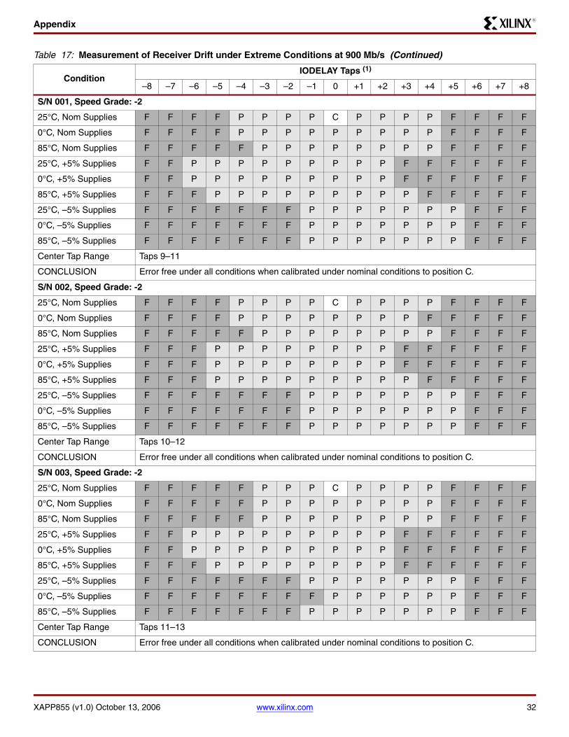
Appendix
XAPP855 (v10) October 13 2006 wwwxilinxcom 32
R
SN 001 Speed Grade -2
25degC Nom Supplies F F F F P P P P C P P P P F F F F
0degC Nom Supplies F F F F P P P P P P P P P F F F F
85degC Nom Supplies F F F F F P P P P P P P P F F F F
25degC +5 Supplies F F P P P P P P P P P F F F F F F
0degC +5 Supplies F F P P P P P P P P P F F F F F F
85degC +5 Supplies F F F P P P P P P P P P F F F F F
25degC ndash5 Supplies F F F F F F F P P P P P P P F F F
0degC ndash5 Supplies F F F F F F F P P P P P P P F F F
85degC ndash5 Supplies F F F F F F F P P P P P P P F F F
Center Tap Range Taps 9ndash11
CONCLUSION Error free under all conditions when calibrated under nominal conditions to position C
SN 002 Speed Grade -2
25degC Nom Supplies F F F F P P P P C P P P P F F F F
0degC Nom Supplies F F F F P P P P P P P P F F F F F
85degC Nom Supplies F F F F F P P P P P P P P F F F F
25degC +5 Supplies F F F P P P P P P P P F F F F F F
0degC +5 Supplies F F F P P P P P P P P F F F F F F
85degC +5 Supplies F F F P P P P P P P P P F F F F F
25degC ndash5 Supplies F F F F F F F P P P P P P P F F F
0degC ndash5 Supplies F F F F F F F P P P P P P P F F F
85degC ndash5 Supplies F F F F F F F P P P P P P P F F F
Center Tap Range Taps 10ndash12
CONCLUSION Error free under all conditions when calibrated under nominal conditions to position C
SN 003 Speed Grade -2
25degC Nom Supplies F F F F F P P P C P P P P F F F F
0degC Nom Supplies F F F F F P P P P P P P P F F F F
85degC Nom Supplies F F F F F P P P P P P P P F F F F
25degC +5 Supplies F F P P P P P P P P P F F F F F F
0degC +5 Supplies F F P P P P P P P P P F F F F F F
85degC +5 Supplies F F F P P P P P P P P F F F F F F
25degC ndash5 Supplies F F F F F F F P P P P P P P F F F
0degC ndash5 Supplies F F F F F F F F P P P P P P F F F
85degC ndash5 Supplies F F F F F F F P P P P P P P F F F
Center Tap Range Taps 11ndash13
CONCLUSION Error free under all conditions when calibrated under nominal conditions to position C
Table 17 Measurement of Receiver Drift under Extreme Conditions at 900 Mbs (Continued)
ConditionIODELAY Taps (1)
ndash8 ndash7 ndash6 ndash5 ndash4 ndash3 ndash2 ndash1 0 +1 +2 +3 +4 +5 +6 +7 +8
Appendix
XAPP855 (v10) October 13 2006 wwwxilinxcom 33
R
SN 004 Speed Grade -3
25degC Nom Supplies F F F F P P P P C P P P P F F F F
0degC Nom Supplies F F F P P P P P P P P P P F F F F
85degC Nom Supplies F F F F P P P P P P P P P F F F F
25degC +5 Supplies F F F P P P P P P P P P F F F F F
0degC +5 Supplies F F F P P P P P P P P P F F F F F
85degC +5 Supplies F F F P P P P P P P P P F F F F F
25degC ndash5 Supplies F F F F F F P P P P P P P P F F F
0degC ndash5 Supplies F F F F F F P P P P P P P P F F F
85degC ndash5 Supplies F F F F F F P P P P P P P P F F F
Center Tap Range Taps 7ndash8
CONCLUSION Error free under all conditions when calibrated under nominal conditions to position C
SN 005 Speed Grade ndash3
25degC Nom Supplies F F F P P P P P C P P P P F F F F
0degC Nom Supplies F F F P P P P P P P P P P F F F F
85degC Nom Supplies F F F F P P P P P P P P P F F F F
25degC +5 Supplies F F P P P P P P P P P P F F F F F
0degC +5 Supplies F F P P P P P P P P P P F F F F F
85degC +5 Supplies F F F P P P P P P P P P F F F F F
25degC ndash5 Supplies F F F F F F P P P P P P P P F F F
0degC ndash5 Supplies F F F F F P P P P P P P P P F F F
85degC ndash5 Supplies F F F F F F P P P P P P P P F F F
Center Tap Range Taps 9ndash10
CONCLUSION Error free under all conditions when calibrated under nominal conditions to position C
SN 006 Speed Grade -3
25degC Nom Supplies F F F F P P P P C P P P P F F F F
0degC Nom Supplies F F F F P P P P P P P P P F F F F
85degC Nom Supplies F F F F P P P P P P P P P F F F F
25degC +5 Supplies F F P P P P P P P P P P F F F F F
0degC +5 Supplies F F P P P P P P P P P P F F F F F
85degC +5 Supplies F F F P P P P P P P P P F F F F F
25degC ndash5 Supplies F F F F F P P P P P P P P P F F F
0degC ndash5 Supplies F F F F F P P P P P P P P P F F F
85degC ndash5 Supplies F F F F F F P P P P P P P P F F F
Center Tap Range Taps 7ndash8
CONCLUSION Error free under all conditions when calibrated under nominal conditions to position C
Notes 1 IODELAY taps where 0 is the reference tap determined by the bit align machine at nominal voltage and 25degC2 P = Error-free transmission F = Error in transmission C = IODELAY tap position selected by bit-align machine under nominal conditions at 25degC
Table 17 Measurement of Receiver Drift under Extreme Conditions at 900 Mbs (Continued)
ConditionIODELAY Taps (1)
ndash8 ndash7 ndash6 ndash5 ndash4 ndash3 ndash2 ndash1 0 +1 +2 +3 +4 +5 +6 +7 +8
Appendix
XAPP855 (v10) October 13 2006 wwwxilinxcom 34
R
Table 18 Measurement of Receiver Drift under Extreme Conditions at 1000 Mbs
ConditionIODELAY Taps (1)
ndash8 ndash7 ndash6 ndash5 ndash4 ndash3 ndash2 ndash1 0 +1 +2 +3 +4 +5 +6 +7 +8
SN 2194 Speed Grade -1
25degC Nom Supplies F F F F F P P P C P P F F F F F F
0degC Nom Supplies F F F F F P P P P P P F F F F F F
85degC Nom Supplies F F F F F P P P P P P F F F F F F
25degC +5 Supplies F F F P P P P P P P F F F F F F F
0degC +5 Supplies F F F P P P P P P P F F F F F F F
85degC +5 Supplies F F F F P P P P P P F F F F F F F
25degC ndash5 Supplies F F F F F F F F P P P P P F F F F
0degC ndash5 Supplies F F F F F F F F P P P P P F F F F
85degC ndash5 Supplies F F F F F F F F P P P P P F F F F
Center Tap Range Taps 12ndash13
CONCLUSION Error free under all conditions when calibrated under nominal conditions to position C
SN 2219 Speed Grade -1
25degC Nom Supplies F F F F F F P P C P P F F F F F F
0degC Nom Supplies F F F F F F P P P P P F F F F F F
85degC Nom Supplies F F F F F F P P P P P F F F F F F
25degC +5 Supplies F F F P P P P P P F F F F F F F F
0degC +5 Supplies F F F P P P P P P F F F F F F F F
85degC +5 Supplies F F F F P P P P P F F F F F F F F
25degC ndash5 Supplies F F F F F F F F F P P P P F F F F
0degC ndash5 Supplies F F F F F F F F F F P P P F F F F
85degC ndash5 Supplies F F F F F F F F F P P P P F F F F
Center Tap Range Taps 14ndash17
CONCLUSION Errors caused by ndash5 variation in supply voltage
SN 2199 Speed Grade -1
25degC Nom Supplies F F F F F F P P C P P F F F F F F
0degC Nom Supplies F F F F F F P P P P P F F F F F F
85degC Nom Supplies F F F F F F P P P P P F F F F F F
25degC +5 Supplies F F F F P P P P P P F F F F F F F
0degC +5 Supplies F F F F P P P P P P F F F F F F F
85degC +5 Supplies F F F F P P P P P P F F F F F F F
25degC ndash5 Supplies F F F F F F F F F P P P P F F F F
0degC ndash5 Supplies F F F F F F F F F P P P P F F F F
85degC ndash5 Supplies F F F F F F F F F P P P P F F F F
Center Tap Range Taps 12ndash14
CONCLUSION Errors caused by ndash5 variation in supply voltage
Appendix
XAPP855 (v10) October 13 2006 wwwxilinxcom 35
R
SN 001 Speed Grade -2
25degC Nom Supplies F F F F F F P P C P P P F F F F F
0degC Nom Supplies F F F F F F P P P P P P F F F F F
85degC Nom Supplies F F F F F F P P P P P P F F F F F
25degC +5 Supplies F F F F P P P P P P F F F F F F F
0degC +5 Supplies F F F F P P P P P P F F F F F F F
85degC +5 Supplies F F F F P P P P P P P F F F F F F
25degC ndash5 Supplies F F F F F F F F F P P P P F F F F
0degC ndash5 Supplies F F F F F F F F F P P P P F F F F
85degC ndash5 Supplies F F F F F F F F F P P P P F F F F
Center Tap Range Taps 11ndash12
CONCLUSION Errors caused by ndash5 variation in supply voltage
SN 002 Speed Grade -2
25degC Nom Supplies F F F F F P P P C P P F F F F F F
0degC Nom Supplies F F F F F P P P P P P P F F F F F
85degC Nom Supplies F F F F F P P P P P P P F F F F F
25degC +5 Supplies F F F F P P P P P P F F F F F F F
0degC +5 Supplies F F F P P P P P P P F F F F F F F
85degC +5 Supplies F F F F P P P P P P P F F F F F F
25degC ndash5 Supplies F F F F F F F P P P P P P F F F F
0degC ndash5 Supplies F F F F F F F P P P P P P F F F F
85degC ndash5 Supplies F F F F F F F P P P P P P F F F F
Center Tap Range Taps 11ndash13
CONCLUSION Error free under all conditions when calibrated under nominal conditions to position C
SN 003 Speed Grade -2
25degC Nom Supplies F F F F F F P P C P P F F F F F F
0degC Nom Supplies F F F F F F P P P P P F F F F F F
85degC Nom Supplies F F F F F F P P P P P F F F F F F
25degC +5 Supplies F F F F P P P P P P F F F F F F F
0degC +5 Supplies F F F F P P P P P P F F F F F F F
85degC +5 Supplies F F F F P P P P P P F F F F F F F
25degC ndash5 Supplies F F F F F F F F F P P P P F F F F
0degC ndash5 Supplies F F F F F F F F F P P P P F F F F
85degC ndash5 Supplies F F F F F F F F F P P P P F F F F
Center Tap Range Taps 13ndash14
CONCLUSION Errors caused by ndash5 variation in supply voltage
Table 18 Measurement of Receiver Drift under Extreme Conditions at 1000 Mbs (Continued)
ConditionIODELAY Taps (1)
ndash8 ndash7 ndash6 ndash5 ndash4 ndash3 ndash2 ndash1 0 +1 +2 +3 +4 +5 +6 +7 +8
Appendix
XAPP855 (v10) October 13 2006 wwwxilinxcom 36
R
SN 004 Speed Grade -3
25degC Nom Supplies F F F F F P P P C P P P F F F F F
0degC Nom Supplies F F F F F P P P P P P P F F F F F
85degC Nom Supplies F F F F F P P P P P P P F F F F F
25degC +5 Supplies F F F P P P P P P P P F F F F F F
0degC +5 Supplies F F F P P P P P P P P F F F F F F
85degC +5 Supplies F F F F P P P P P P P P F F F F F
25degC ndash5 Supplies F F F F F F F P P P P P P F F F F
0degC ndash5 Supplies F F F F F F F P P P P P P F F F F
85degC ndash5 Supplies F F F F F F F P P P P P P P F F F
Center Tap Range Taps 9ndash10
CONCLUSION Error free under all conditions when calibrated under nominal conditions to position C
SN 005 Speed Grade -3
25degC Nom Supplies F F F F P P P P C P P P F F F F F
0degC Nom Supplies F F F F P P P P P P P P F F F F F
85degC Nom Supplies F F F F P P P P P P P P F F F F F
25degC +5 Supplies F F F P P P P P P P P F F F F F F
0degC +5 Supplies F F P P P P P P P P P F F F F F F
85degC +5 Supplies F F F P P P P P P P P F F F F F F
25degC ndash5 Supplies F F F F F F P P P P P P P P F F F
0degC ndash5 Supplies F F F F F F P P P P P P P P F F F
85degC ndash5 Supplies F F F F F F P P P P P P P F F F F
Center Tap Range Taps 11ndash12
CONCLUSION Error free under all conditions when calibrated under nominal conditions to position C
SN 006 Speed Grade -3
25degC Nom Supplies F F F F P P P P C P P P F F F F F
0degC Nom Supplies F F F F P P P P P P P P F F F F F
85degC Nom Supplies F F F F P P P P P P P P F F F F F
25degC +5 Supplies F F F P P P P P P P P F F F F F F
0degC +5 Supplies F F F P P P P P P P P F F F F F F
85degC +5 Supplies F F F P P P P P P P P F F F F F F
25degC ndash5 Supplies F F F F F F P P P P P P P F F F F
0degC ndash5 Supplies F F F F F F P P P P P P P F F F F
85degC ndash5 Supplies F F F F F F P P P P P P P F F F F
Center Tap Range Taps 9ndash10
CONCLUSION Error free under all conditions when calibrated under nominal conditions to position C
Notes 1 IODELAY taps where 0 is the reference tap determined by the bit align machine at nominal voltage and 25degC2 P = Error-free transmission F = Error in transmission C = IODELAY tap position selected by bit-align machine under nominal conditions at 25degC
Table 18 Measurement of Receiver Drift under Extreme Conditions at 1000 Mbs (Continued)
ConditionIODELAY Taps (1)
ndash8 ndash7 ndash6 ndash5 ndash4 ndash3 ndash2 ndash1 0 +1 +2 +3 +4 +5 +6 +7 +8
Appendix
XAPP855 (v10) October 13 2006 wwwxilinxcom 37
R
Table 19 Measurement of Receiver Drift under Extreme Conditions at 1100 Mbs
ConditionIODELAY Taps (1)
ndash8 ndash7 ndash6 ndash5 ndash4 ndash3 ndash2 ndash1 0 +1 +2 +3 +4 +5 +6 +7 +8
SN 2194 Speed Grade -1
25degC Nom Supplies F F F F F F P P C P P F F F F F F
0degC Nom Supplies F F F F F F P P P P P F F F F F F
85degC Nom Supplies F F F F F F P P P P P F F F F F F
25degC +5 Supplies F F F F P P P P P F F F F F F F F
0degC +5 Supplies F F F F P P P P P F F F F F F F F
85degC +5 Supplies F F F F P P P P P F F F F F F F F
25degC ndash5 Supplies F F F F F F F F F P P P F F F F F
0degC ndash5 Supplies F F F F F F F F F P P P F F F F F
85degC ndash5 Supplies F F F F F F F F F P P P F F F F F
Center Tap Range Taps 13ndash14
CONCLUSION Errors caused by ndash5 variation in supply voltage
SN 2219 Speed Grade -1
25degC Nom Supplies F F F F F F P P C P F F F F F F F
0degC Nom Supplies F F F F F F P P P P F F F F F F F
85degC Nom Supplies F F F F F F P P P P F F F F F F F
25degC +5 Supplies F F F F P P P P F F F F F F F F F
0degC +5 Supplies F F F F P P P P F F F F F F F F F
85degC +5 Supplies F F F F P P P P F F F F F F F F F
25degC ndash5 Supplies F F F F F F F F F F P P F F F F F
0degC ndash5 Supplies F F F F F F F F F F P P F F F F F
85degC ndash5 Supplies F F F F F F F F F P P P F F F F F
Center Tap Range Taps 6 15ndash17
CONCLUSION Errors caused by plusmn5 variation in supply voltage
SN 2199 Speed Grade -1
25degC Nom Supplies F F F F F F F P C P F F F F F F F
0degC Nom Supplies F F F F F F F P P P F F F F F F F
85degC Nom Supplies F F F F F F F P P P F F F F F F F
25degC +5 Supplies F F F F P P P P P F F F F F F F F
0degC +5 Supplies F F F F P P P P P F F F F F F F F
85degC +5 Supplies F F F F F P P P P F F F F F F F F
25degC ndash5 Supplies F F F F F F F F F F P P F F F F F
0degC ndash5 Supplies F F F F F F F F F F P P F F F F F
85degC ndash5 Supplies F F F F F F F F F F P P F F F F F
Center Tap Range Taps 13ndash15
CONCLUSION Errors caused by ndash5 variation in supply voltage
Appendix
XAPP855 (v10) October 13 2006 wwwxilinxcom 38
R
SN 001 Speed Grade -2
25degC Nom Supplies F F F F F F P P C P P F F F F F F
0degC Nom Supplies F F F F F F P P P P P F F F F F F
85degC Nom Supplies F F F F F F P P P P P F F F F F F
25degC +5 Supplies F F F F P P P P P F F F F F F F F
0degC +5 Supplies F F F F P P P P P F F F F F F F F
85degC +5 Supplies F F F F P P P P P F F F F F F F F
25degC ndash5 Supplies F F F F F F F F P P P P F F F F F
0degC ndash5 Supplies F F F F F F F F P P P P F F F F F
85degC ndash5 Supplies F F F F F F F F P P P P F F F F F
Center Tap Range Taps 12ndash13
CONCLUSION Error free under all conditions when calibrated under nominal conditions to position C
SN 002 Speed Grade -2
25degC Nom Supplies F F F F F P P P C P F F F F F F F
0degC Nom Supplies F F F F F P P P P P F F F F F F F
85degC Nom Supplies F F F F F F P P P P F F F F F F F
25degC +5 Supplies F F F F P P P P P F F F F F F F F
0degC +5 Supplies F F F P P P P P P F F F F F F F F
85degC +5 Supplies F F F F P P P P P F F F F F F F F
25degC ndash5 Supplies F F F F F F F F P P P P F F F F F
0degC ndash5 Supplies F F F F F F F F P P P P F F F F F
85degC ndash5 Supplies F F F F F F F F P P P P F F F F F
Center Tap Range Taps 13ndash14
CONCLUSION Error free under all conditions when calibrated under nominal conditions to position C
SN 003 Speed Grade -2
25degC Nom Supplies F F F F F F F P C P F F F F F F F
0degC Nom Supplies F F F F F F F P P P F F F F F F F
85degC Nom Supplies F F F F F F F P P P P F F F F F F
25degC +5 Supplies F F F F F P P P P F F F F F F F F
0degC +5 Supplies F F F F F P P P P F F F F F F F F
85degC +5 Supplies F F F F F P P P P F F F F F F F F
25degC ndash5 Supplies F F F F F F F F F F P P F F F F F
0degC ndash5 Supplies F F F F F F F F F F P P F F F F F
85degC ndash5 Supplies F F F F F F F F F P P P F F F F F
Center Tap Range Taps 14ndash16
CONCLUSION Errors caused by ndash5 variation in supply voltage
Table 19 Measurement of Receiver Drift under Extreme Conditions at 1100 Mbs (Continued)
ConditionIODELAY Taps (1)
ndash8 ndash7 ndash6 ndash5 ndash4 ndash3 ndash2 ndash1 0 +1 +2 +3 +4 +5 +6 +7 +8
Appendix
XAPP855 (v10) October 13 2006 wwwxilinxcom 39
R
SN 004 Speed Grade -3
25degC Nom Supplies F F F F F P P P C P P F F F F F F
0degC Nom Supplies F F F F F P P P P P P F F F F F F
85degC Nom Supplies F F F F F F P P P P P F F F F F F
25degC +5 Supplies F F F F P P P P P P F F F F F F F
0degC +5 Supplies F F F F P P P P P P F F F F F F F
85degC +5 Supplies F F F F P P P P P P F F F F F F F
25degC ndash5 Supplies F F F F F F F F P P P P F F F F F
0degC ndash5 Supplies F F F F F F F P P P P P F F F F F
85degC ndash5 Supplies F F F F F F F F P P P P P F F F F
Center Tap Range Taps 9ndash10
CONCLUSION Error free under all conditions when calibrated under nominal conditions to position C
SN 005 Speed Grade -3
25degC Nom Supplies F F F F F P P P C P P F F F F F F
0degC Nom Supplies F F F F F P P P P P P F F F F F F
85degC Nom Supplies F F F F F F P P P P P F F F F F F
25degC +5 Supplies F F F F P P P P P P F F F F F F F
0degC +5 Supplies F F F F P P P P P P F F F F F F F
85degC +5 Supplies F F F F P P P P P P F F F F F F F
25degC ndash5 Supplies F F F F F F F P P P P P P F F F F
0degC ndash5 Supplies F F F F F F F P P P P P P F F F F
85degC ndash5 Supplies F F F F F F F P P P P P P F F F F
Center Tap Range Taps 11ndash12
CONCLUSION Error free under all conditions when calibrated under nominal conditions to position C
SN 006 Speed Grade -3
25degC Nom Supplies F F F F F P P P C P P P F F F F F
0degC Nom Supplies F F F F F P P P P P P F F F F F F
85degC Nom Supplies F F F F F P P P P P P P F F F F F
25degC +5 Supplies F F F F P P P P P P P F F F F F F
0degC +5 Supplies F F F P P P P P P P F F F F F F F
85degC +5 Supplies F F F F P P P P P P P F F F F F F
25degC ndash5 Supplies F F F F F F P P P P P P P F F F F
0degC ndash5 Supplies F F F F F F P P P P P P P F F F F
85degC ndash5 Supplies F F F F F F F P P P P P P F F F F
Center Tap Range Taps 9ndash10
CONCLUSION Error free under all conditions when calibrated under nominal conditions to position C
Notes 1 IODELAY taps where 0 is the reference tap determined by the bit align machine at nominal voltage and 25degC2 P = Error-free transmission F = Error in transmission C = IODELAY tap position selected by bit-align machine under nominal conditions at 25degC
Table 19 Measurement of Receiver Drift under Extreme Conditions at 1100 Mbs (Continued)
ConditionIODELAY Taps (1)
ndash8 ndash7 ndash6 ndash5 ndash4 ndash3 ndash2 ndash1 0 +1 +2 +3 +4 +5 +6 +7 +8
Appendix
XAPP855 (v10) October 13 2006 wwwxilinxcom 40
R
Table 20 Measurement of Receiver Drift under Extreme Conditions at 1200 Mbs
ConditionIODELAY Taps (1)
ndash8 ndash7 ndash6 ndash5 ndash4 ndash3 ndash2 ndash1 0 +1 +2 +3 +4 +5 +6 +7 +8
SN 2194 Speed Grade -1
25degC Nom Supplies F F F F F F F P C F F F F F F F F
0degC Nom Supplies F F F F F F F P P F F F F F F F F
85degC Nom Supplies F F F F F F F P P F F F F F F F F
25degC +5 Supplies F F F F P P P P F F F F F F F F F
0degC +5 Supplies F F F F P P P P F F F F F F F F F
85degC +5 Supplies F F F F F P P P F F F F F F F F F
25degC ndash5 Supplies F F F F F F F F F P P F F F F F F
0degC ndash5 Supplies F F F F F F F F F F P F F F F F F
85degC ndash5 Supplies F F F F F F F F F P F F F F F F F
Center Tap Range Taps 13ndash15
CONCLUSION Errors caused by plusmn5 variation in supply voltage
SN 2219 Speed Grade -1
25degC Nom Supplies F F F F F F F F C F F F F F F F F
0degC Nom Supplies F F F F F F F P P F F F F F F F F
85degC Nom Supplies F F F F F F F F P F F F F F F F F
25degC +5 Supplies F F F F F P P P F F F F F F F F F
0degC +5 Supplies F F F F F P P P F F F F F F F F F
85degC +5 Supplies F F F F F F P P F F F F F F F F F
25degC ndash5 Supplies F F F F F F F F F F F F F F F F F
0degC ndash5 Supplies F F F F F F F F F F F F F F F F F
85degC ndash5 Supplies F F F F F F F F F F F F F F F F F
Center Tap Range Taps 6ndash7 16ndash17
CONCLUSION Errors caused by plusmn5 variation in supply voltage
SN 2199 Speed Grade -1
25degC Nom Supplies F F F F F F F P C F F F F F F F F
0degC Nom Supplies F F F F F F F P P F F F F F F F F
85degC Nom Supplies F F F F F F F F P F F F F F F F F
25degC +5 Supplies F F F F F P P P F F F F F F F F F
0degC +5 Supplies F F F F F P P P F F F F F F F F F
85degC +5 Supplies F F F F F P P P F F F F F F F F F
25degC ndash5 Supplies F F F F F F F F F F F F F F F F F
0degC ndash5 Supplies F F F F F F F F F F F F F F F F F
85degC ndash5 Supplies F F F F F F F F F F F F F F F F F
Center Tap Range Taps 13ndash15
CONCLUSION Errors caused by plusmn5 variation in supply voltage
Appendix
XAPP855 (v10) October 13 2006 wwwxilinxcom 41
R
SN 001 Speed Grade -2
25degC Nom Supplies F F F F F F F P C P F F F F F F F
0degC Nom Supplies F F F F F F F P P P F F F F F F F
85degC Nom Supplies F F F F F F F P P P F F F F F F F
25degC +5 Supplies F F F F F P P P P F F F F F F F F
0degC +5 Supplies F F F F P P P P P F F F F F F F F
85degC +5 Supplies F F F F F P P P P F F F F F F F F
25degC ndash5 Supplies F F F F F F F F F F P F F F F F F
0degC ndash5 Supplies F F F F F F F F F F P F F F F F F
85degC ndash5 Supplies F F F F F F F F F F P F F F F F F
Center Tap Range Taps 12ndash13
CONCLUSION Errors caused by ndash5 variation in supply voltage
SN 002 Speed Grade -2
25degC Nom Supplies F F F F F F P P C P F F F F F F F
0degC Nom Supplies F F F F F F P P P P F F F F F F F
85degC Nom Supplies F F F F F F F P P P F F F F F F F
25degC +5 Supplies F F F F P P P P F F F F F F F F F
0degC +5 Supplies F F F F P P P P F F F F F F F F F
85degC +5 Supplies F F F F F P P P F F F F F F F F F
25degC ndash5 Supplies F F F F F F F F P P P F F F F F F
0degC ndash5 Supplies F F F F F F F F P P P F F F F F F
85degC ndash5 Supplies F F F F F F F F F P P F F F F F F
Center Tap Range Taps 13ndash14
CONCLUSION Errors caused by plusmn5 variation in supply voltage
SN 003 Speed Grade -2
25degC Nom Supplies F F F F F F F P C F F F F F F F F
0degC Nom Supplies F F F F F F F P P F F F F F F F F
85degC Nom Supplies F F F F F F F F P F F F F F F F F
25degC +5 Supplies F F F F F P P P F F F F F F F F F
0degC +5 Supplies F F F F F P P P F F F F F F F F F
85degC +5 Supplies F F F F F F P P F F F F F F F F F
25degC ndash5 Supplies F F F F F F F F F F F F F F F F F
0degC ndash5 Supplies F F F F F F F F F F F F F F F F F
85degC ndash5 Supplies F F F F F F F F F F F F F F F F F
Center Tap Range Taps 14ndash15
CONCLUSION Errors caused by plusmn5 variation in supply voltage
Table 20 Measurement of Receiver Drift under Extreme Conditions at 1200 Mbs (Continued)
ConditionIODELAY Taps (1)
ndash8 ndash7 ndash6 ndash5 ndash4 ndash3 ndash2 ndash1 0 +1 +2 +3 +4 +5 +6 +7 +8
Appendix
XAPP855 (v10) October 13 2006 wwwxilinxcom 42
R
SN 004 Speed Grade -3
25degC Nom Supplies F F F F F F P P C P F F F F F F F
0degC Nom Supplies F F F F F P P P P P F F F F F F F
85degC Nom Supplies F F F F F F P P P P F F F F F F F
25degC +5 Supplies F F F F P P P P P F F F F F F F F
0degC +5 Supplies F F F F P P P P P F F F F F F F F
85degC +5 Supplies F F F F F P P P P F F F F F F F F
25degC ndash5 Supplies F F F F F F F F P P P F F F F F F
0degC ndash5 Supplies F F F F F F F F P P P F F F F F F
85degC ndash5 Supplies F F F F F F F F P P P F F F F F F
Center Tap Range Taps 9ndash11
CONCLUSION Error free under all conditions when calibrated under nominal conditions to position C
SN 005 Speed Grade -3
25degC Nom Supplies F F F F F P P P C P F F F F F F F
0degC Nom Supplies F F F F F P P P P P F F F F F F F
85degC Nom Supplies F F F F F F P P P P F F F F F F F
25degC +5 Supplies F F F F P P P P P F F F F F F F F
0degC +5 Supplies F F F P P P P P P F F F F F F F F
85degC +5 Supplies F F F F P P P P P F F F F F F F F
25degC ndash5 Supplies F F F F F F F P P P P P F F F F F
0degC ndash5 Supplies F F F F F F F P P P P P F F F F F
85degC ndash5 Supplies F F F F F F F F P P P F F F F F F
Center Tap Range Taps 11ndash13
CONCLUSION Error free under all conditions when calibrated under nominal conditions to position C
SN 006 Speed Grade -3
25degC Nom Supplies F F F F F P P P C P F F F F F F F
0degC Nom Supplies F F F F F P P P P P F F F F F F F
85degC Nom Supplies F F F F F P P P P P F F F F F F F
25degC +5 Supplies F F F P P P P P P F F F F F F F F
0degC +5 Supplies F F F P P P P P P F F F F F F F F
85degC +5 Supplies F F F F P P P P P F F F F F F F F
25degC ndash5 Supplies F F F F F F F P P P P F F F F F F
0degC ndash5 Supplies F F F F F F P P P P P F F F F F F
85degC ndash5 Supplies F F F F F F F P P P P F F F F F F
Center Tap Range Taps 10ndash11
CONCLUSION Error free under all conditions when calibrated under nominal conditions to position C
Notes 1 IODELAY taps where 0 is the reference tap determined by the bit align machine at nominal voltage and 25degC2 P = Error-free transmission F = Error in transmission C = IODELAY tap position selected by bit-align machine under nominal conditions at 25degC
Table 20 Measurement of Receiver Drift under Extreme Conditions at 1200 Mbs (Continued)
ConditionIODELAY Taps (1)
ndash8 ndash7 ndash6 ndash5 ndash4 ndash3 ndash2 ndash1 0 +1 +2 +3 +4 +5 +6 +7 +8
Revision History
XAPP855 (v10) October 13 2006 wwwxilinxcom 43
R
Revision History
The following table shows the revision history for this document
Date Version Revision
101306 10 Initial Xilinx release
- 16-Channel DDR LVDS Interface with Per-Channel Alignment
-
- Summary
- Introduction
-
- Figure 1 Full-Duplex 16-Channel DDR Link between a Virtex-5 Device and Another Device with a 16-Channel DDR Interface
- Figure 2 BERT Testbench for Hardware Verification of the DDR Interface
- Figure 3 Design Hierarchy of the Interface (TX and RX)
-
- DDR Transmitter
-
- Table 1 DDR_8TO1_16CHAN_TX Module Port Definitions
- Figure 4 MasterSlave OSERDES Pair for a Single Data Channel with 81 Serialization
- Figure 5 Block Diagram of TX Interface
- Table 2 DDR TX Interface Utilization Statistics
-
- Interface Clocking
-
- Figure 6 Global and Regional Clocking Schemes in Virtex-5 FPGAs
- Table 3 Comparison of Global and IO Clock Performance by Speed Grade
-
- DDR Receiver
-
- Table 4 DDR_8TO1_16CHAN_RX Module Port Definitions
- Figure 7 MasterSlave ISERDES Pair for a Single Data Channel with 18 Deserialization
- Figure 8 Block Diagram of RX Interface
- Table 5 DDR RX Interface Utilization Statistics
-
- Receiver Interface Dynamic Timing
-
- Inherent Timing
-
- Figure 9 Timing Components of RX Data and Clock Paths
- Figure 10 ISE Timing Analyzer Properties Used in this Document
- Table 6 Datapath Timing Definitions
- Table 7 Clock Path Timing Definitions
- Table 8 Datapath Delay Inventory for a -1 Speed Grade XC5VLX50T Device
- Table 9 Clock Path Delay Inventory for a -1 Speed Grade XC5VLX50T Device
- Figure 11 Timing Windows Show Uncertainty in ClockData Relationship as Calculated by Timing Analyzer
-
- Dynamic Timing and BIT_ALIGN_MACHINE
-
- Figure 12 Inherent Timing Windows Shown in Relation to Multiple Data Rates
- Figure 13 Dynamic Bit-Alignment Procedure in BIT_ALIGN_MACHINE
- Table 10 Word Alignment in the DDR Receiver
- Figure 14 FSM in the BIT_ALIGN_MACHINE Module
-
- Interface Timing Budget
-
- Interface Characterization
-
- Figure 15 Bit-Alignment Algorithm Performance
- Table 11 Tap Setting Range For Various Data Rates Measured on a -2 Device
- Table 12 Measurement of Receiver Drift under Extreme Conditions for Multiple Data Rates
- Pattern Dependence of Receiver Performance
-
- Table 13 Link Performance for Various Types of Data Measured on a -2 Device
-
- Resetting the Interface
-
- Figure 16 Recommended Interface Reset Timing
-
- Conclusion
-
- Table 14 Performance of 16-Channel DDR Interface
-
- Appendix
-
- Performance Characterization Data
-
- Table 15 Summary of Interface Characterization Results
- Table 16 Measurement of Receiver Drift under Extreme Conditions at 800 Mbs
- Table 17 Measurement of Receiver Drift under Extreme Conditions at 900 Mbs
- Table 18 Measurement of Receiver Drift under Extreme Conditions at 1000 Mbs
- Table 19 Measurement of Receiver Drift under Extreme Conditions at 1100 Mbs
- Table 20 Measurement of Receiver Drift under Extreme Conditions at 1200 Mbs
-
- Revision History
-
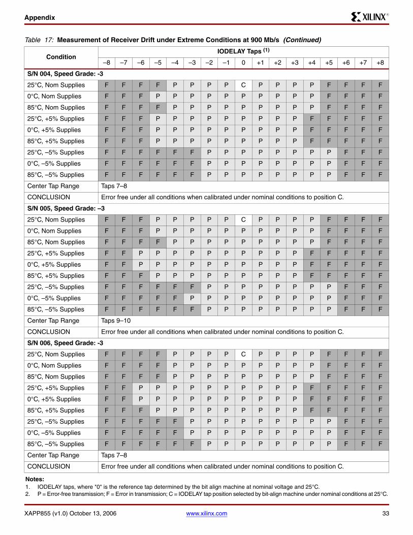
Appendix
XAPP855 (v10) October 13 2006 wwwxilinxcom 33
R
SN 004 Speed Grade -3
25degC Nom Supplies F F F F P P P P C P P P P F F F F
0degC Nom Supplies F F F P P P P P P P P P P F F F F
85degC Nom Supplies F F F F P P P P P P P P P F F F F
25degC +5 Supplies F F F P P P P P P P P P F F F F F
0degC +5 Supplies F F F P P P P P P P P P F F F F F
85degC +5 Supplies F F F P P P P P P P P P F F F F F
25degC ndash5 Supplies F F F F F F P P P P P P P P F F F
0degC ndash5 Supplies F F F F F F P P P P P P P P F F F
85degC ndash5 Supplies F F F F F F P P P P P P P P F F F
Center Tap Range Taps 7ndash8
CONCLUSION Error free under all conditions when calibrated under nominal conditions to position C
SN 005 Speed Grade ndash3
25degC Nom Supplies F F F P P P P P C P P P P F F F F
0degC Nom Supplies F F F P P P P P P P P P P F F F F
85degC Nom Supplies F F F F P P P P P P P P P F F F F
25degC +5 Supplies F F P P P P P P P P P P F F F F F
0degC +5 Supplies F F P P P P P P P P P P F F F F F
85degC +5 Supplies F F F P P P P P P P P P F F F F F
25degC ndash5 Supplies F F F F F F P P P P P P P P F F F
0degC ndash5 Supplies F F F F F P P P P P P P P P F F F
85degC ndash5 Supplies F F F F F F P P P P P P P P F F F
Center Tap Range Taps 9ndash10
CONCLUSION Error free under all conditions when calibrated under nominal conditions to position C
SN 006 Speed Grade -3
25degC Nom Supplies F F F F P P P P C P P P P F F F F
0degC Nom Supplies F F F F P P P P P P P P P F F F F
85degC Nom Supplies F F F F P P P P P P P P P F F F F
25degC +5 Supplies F F P P P P P P P P P P F F F F F
0degC +5 Supplies F F P P P P P P P P P P F F F F F
85degC +5 Supplies F F F P P P P P P P P P F F F F F
25degC ndash5 Supplies F F F F F P P P P P P P P P F F F
0degC ndash5 Supplies F F F F F P P P P P P P P P F F F
85degC ndash5 Supplies F F F F F F P P P P P P P P F F F
Center Tap Range Taps 7ndash8
CONCLUSION Error free under all conditions when calibrated under nominal conditions to position C
Notes 1 IODELAY taps where 0 is the reference tap determined by the bit align machine at nominal voltage and 25degC2 P = Error-free transmission F = Error in transmission C = IODELAY tap position selected by bit-align machine under nominal conditions at 25degC
Table 17 Measurement of Receiver Drift under Extreme Conditions at 900 Mbs (Continued)
ConditionIODELAY Taps (1)
ndash8 ndash7 ndash6 ndash5 ndash4 ndash3 ndash2 ndash1 0 +1 +2 +3 +4 +5 +6 +7 +8
Appendix
XAPP855 (v10) October 13 2006 wwwxilinxcom 34
R
Table 18 Measurement of Receiver Drift under Extreme Conditions at 1000 Mbs
ConditionIODELAY Taps (1)
ndash8 ndash7 ndash6 ndash5 ndash4 ndash3 ndash2 ndash1 0 +1 +2 +3 +4 +5 +6 +7 +8
SN 2194 Speed Grade -1
25degC Nom Supplies F F F F F P P P C P P F F F F F F
0degC Nom Supplies F F F F F P P P P P P F F F F F F
85degC Nom Supplies F F F F F P P P P P P F F F F F F
25degC +5 Supplies F F F P P P P P P P F F F F F F F
0degC +5 Supplies F F F P P P P P P P F F F F F F F
85degC +5 Supplies F F F F P P P P P P F F F F F F F
25degC ndash5 Supplies F F F F F F F F P P P P P F F F F
0degC ndash5 Supplies F F F F F F F F P P P P P F F F F
85degC ndash5 Supplies F F F F F F F F P P P P P F F F F
Center Tap Range Taps 12ndash13
CONCLUSION Error free under all conditions when calibrated under nominal conditions to position C
SN 2219 Speed Grade -1
25degC Nom Supplies F F F F F F P P C P P F F F F F F
0degC Nom Supplies F F F F F F P P P P P F F F F F F
85degC Nom Supplies F F F F F F P P P P P F F F F F F
25degC +5 Supplies F F F P P P P P P F F F F F F F F
0degC +5 Supplies F F F P P P P P P F F F F F F F F
85degC +5 Supplies F F F F P P P P P F F F F F F F F
25degC ndash5 Supplies F F F F F F F F F P P P P F F F F
0degC ndash5 Supplies F F F F F F F F F F P P P F F F F
85degC ndash5 Supplies F F F F F F F F F P P P P F F F F
Center Tap Range Taps 14ndash17
CONCLUSION Errors caused by ndash5 variation in supply voltage
SN 2199 Speed Grade -1
25degC Nom Supplies F F F F F F P P C P P F F F F F F
0degC Nom Supplies F F F F F F P P P P P F F F F F F
85degC Nom Supplies F F F F F F P P P P P F F F F F F
25degC +5 Supplies F F F F P P P P P P F F F F F F F
0degC +5 Supplies F F F F P P P P P P F F F F F F F
85degC +5 Supplies F F F F P P P P P P F F F F F F F
25degC ndash5 Supplies F F F F F F F F F P P P P F F F F
0degC ndash5 Supplies F F F F F F F F F P P P P F F F F
85degC ndash5 Supplies F F F F F F F F F P P P P F F F F
Center Tap Range Taps 12ndash14
CONCLUSION Errors caused by ndash5 variation in supply voltage
Appendix
XAPP855 (v10) October 13 2006 wwwxilinxcom 35
R
SN 001 Speed Grade -2
25degC Nom Supplies F F F F F F P P C P P P F F F F F
0degC Nom Supplies F F F F F F P P P P P P F F F F F
85degC Nom Supplies F F F F F F P P P P P P F F F F F
25degC +5 Supplies F F F F P P P P P P F F F F F F F
0degC +5 Supplies F F F F P P P P P P F F F F F F F
85degC +5 Supplies F F F F P P P P P P P F F F F F F
25degC ndash5 Supplies F F F F F F F F F P P P P F F F F
0degC ndash5 Supplies F F F F F F F F F P P P P F F F F
85degC ndash5 Supplies F F F F F F F F F P P P P F F F F
Center Tap Range Taps 11ndash12
CONCLUSION Errors caused by ndash5 variation in supply voltage
SN 002 Speed Grade -2
25degC Nom Supplies F F F F F P P P C P P F F F F F F
0degC Nom Supplies F F F F F P P P P P P P F F F F F
85degC Nom Supplies F F F F F P P P P P P P F F F F F
25degC +5 Supplies F F F F P P P P P P F F F F F F F
0degC +5 Supplies F F F P P P P P P P F F F F F F F
85degC +5 Supplies F F F F P P P P P P P F F F F F F
25degC ndash5 Supplies F F F F F F F P P P P P P F F F F
0degC ndash5 Supplies F F F F F F F P P P P P P F F F F
85degC ndash5 Supplies F F F F F F F P P P P P P F F F F
Center Tap Range Taps 11ndash13
CONCLUSION Error free under all conditions when calibrated under nominal conditions to position C
SN 003 Speed Grade -2
25degC Nom Supplies F F F F F F P P C P P F F F F F F
0degC Nom Supplies F F F F F F P P P P P F F F F F F
85degC Nom Supplies F F F F F F P P P P P F F F F F F
25degC +5 Supplies F F F F P P P P P P F F F F F F F
0degC +5 Supplies F F F F P P P P P P F F F F F F F
85degC +5 Supplies F F F F P P P P P P F F F F F F F
25degC ndash5 Supplies F F F F F F F F F P P P P F F F F
0degC ndash5 Supplies F F F F F F F F F P P P P F F F F
85degC ndash5 Supplies F F F F F F F F F P P P P F F F F
Center Tap Range Taps 13ndash14
CONCLUSION Errors caused by ndash5 variation in supply voltage
Table 18 Measurement of Receiver Drift under Extreme Conditions at 1000 Mbs (Continued)
ConditionIODELAY Taps (1)
ndash8 ndash7 ndash6 ndash5 ndash4 ndash3 ndash2 ndash1 0 +1 +2 +3 +4 +5 +6 +7 +8
Appendix
XAPP855 (v10) October 13 2006 wwwxilinxcom 36
R
SN 004 Speed Grade -3
25degC Nom Supplies F F F F F P P P C P P P F F F F F
0degC Nom Supplies F F F F F P P P P P P P F F F F F
85degC Nom Supplies F F F F F P P P P P P P F F F F F
25degC +5 Supplies F F F P P P P P P P P F F F F F F
0degC +5 Supplies F F F P P P P P P P P F F F F F F
85degC +5 Supplies F F F F P P P P P P P P F F F F F
25degC ndash5 Supplies F F F F F F F P P P P P P F F F F
0degC ndash5 Supplies F F F F F F F P P P P P P F F F F
85degC ndash5 Supplies F F F F F F F P P P P P P P F F F
Center Tap Range Taps 9ndash10
CONCLUSION Error free under all conditions when calibrated under nominal conditions to position C
SN 005 Speed Grade -3
25degC Nom Supplies F F F F P P P P C P P P F F F F F
0degC Nom Supplies F F F F P P P P P P P P F F F F F
85degC Nom Supplies F F F F P P P P P P P P F F F F F
25degC +5 Supplies F F F P P P P P P P P F F F F F F
0degC +5 Supplies F F P P P P P P P P P F F F F F F
85degC +5 Supplies F F F P P P P P P P P F F F F F F
25degC ndash5 Supplies F F F F F F P P P P P P P P F F F
0degC ndash5 Supplies F F F F F F P P P P P P P P F F F
85degC ndash5 Supplies F F F F F F P P P P P P P F F F F
Center Tap Range Taps 11ndash12
CONCLUSION Error free under all conditions when calibrated under nominal conditions to position C
SN 006 Speed Grade -3
25degC Nom Supplies F F F F P P P P C P P P F F F F F
0degC Nom Supplies F F F F P P P P P P P P F F F F F
85degC Nom Supplies F F F F P P P P P P P P F F F F F
25degC +5 Supplies F F F P P P P P P P P F F F F F F
0degC +5 Supplies F F F P P P P P P P P F F F F F F
85degC +5 Supplies F F F P P P P P P P P F F F F F F
25degC ndash5 Supplies F F F F F F P P P P P P P F F F F
0degC ndash5 Supplies F F F F F F P P P P P P P F F F F
85degC ndash5 Supplies F F F F F F P P P P P P P F F F F
Center Tap Range Taps 9ndash10
CONCLUSION Error free under all conditions when calibrated under nominal conditions to position C
Notes 1 IODELAY taps where 0 is the reference tap determined by the bit align machine at nominal voltage and 25degC2 P = Error-free transmission F = Error in transmission C = IODELAY tap position selected by bit-align machine under nominal conditions at 25degC
Table 18 Measurement of Receiver Drift under Extreme Conditions at 1000 Mbs (Continued)
ConditionIODELAY Taps (1)
ndash8 ndash7 ndash6 ndash5 ndash4 ndash3 ndash2 ndash1 0 +1 +2 +3 +4 +5 +6 +7 +8
Appendix
XAPP855 (v10) October 13 2006 wwwxilinxcom 37
R
Table 19 Measurement of Receiver Drift under Extreme Conditions at 1100 Mbs
ConditionIODELAY Taps (1)
ndash8 ndash7 ndash6 ndash5 ndash4 ndash3 ndash2 ndash1 0 +1 +2 +3 +4 +5 +6 +7 +8
SN 2194 Speed Grade -1
25degC Nom Supplies F F F F F F P P C P P F F F F F F
0degC Nom Supplies F F F F F F P P P P P F F F F F F
85degC Nom Supplies F F F F F F P P P P P F F F F F F
25degC +5 Supplies F F F F P P P P P F F F F F F F F
0degC +5 Supplies F F F F P P P P P F F F F F F F F
85degC +5 Supplies F F F F P P P P P F F F F F F F F
25degC ndash5 Supplies F F F F F F F F F P P P F F F F F
0degC ndash5 Supplies F F F F F F F F F P P P F F F F F
85degC ndash5 Supplies F F F F F F F F F P P P F F F F F
Center Tap Range Taps 13ndash14
CONCLUSION Errors caused by ndash5 variation in supply voltage
SN 2219 Speed Grade -1
25degC Nom Supplies F F F F F F P P C P F F F F F F F
0degC Nom Supplies F F F F F F P P P P F F F F F F F
85degC Nom Supplies F F F F F F P P P P F F F F F F F
25degC +5 Supplies F F F F P P P P F F F F F F F F F
0degC +5 Supplies F F F F P P P P F F F F F F F F F
85degC +5 Supplies F F F F P P P P F F F F F F F F F
25degC ndash5 Supplies F F F F F F F F F F P P F F F F F
0degC ndash5 Supplies F F F F F F F F F F P P F F F F F
85degC ndash5 Supplies F F F F F F F F F P P P F F F F F
Center Tap Range Taps 6 15ndash17
CONCLUSION Errors caused by plusmn5 variation in supply voltage
SN 2199 Speed Grade -1
25degC Nom Supplies F F F F F F F P C P F F F F F F F
0degC Nom Supplies F F F F F F F P P P F F F F F F F
85degC Nom Supplies F F F F F F F P P P F F F F F F F
25degC +5 Supplies F F F F P P P P P F F F F F F F F
0degC +5 Supplies F F F F P P P P P F F F F F F F F
85degC +5 Supplies F F F F F P P P P F F F F F F F F
25degC ndash5 Supplies F F F F F F F F F F P P F F F F F
0degC ndash5 Supplies F F F F F F F F F F P P F F F F F
85degC ndash5 Supplies F F F F F F F F F F P P F F F F F
Center Tap Range Taps 13ndash15
CONCLUSION Errors caused by ndash5 variation in supply voltage
Appendix
XAPP855 (v10) October 13 2006 wwwxilinxcom 38
R
SN 001 Speed Grade -2
25degC Nom Supplies F F F F F F P P C P P F F F F F F
0degC Nom Supplies F F F F F F P P P P P F F F F F F
85degC Nom Supplies F F F F F F P P P P P F F F F F F
25degC +5 Supplies F F F F P P P P P F F F F F F F F
0degC +5 Supplies F F F F P P P P P F F F F F F F F
85degC +5 Supplies F F F F P P P P P F F F F F F F F
25degC ndash5 Supplies F F F F F F F F P P P P F F F F F
0degC ndash5 Supplies F F F F F F F F P P P P F F F F F
85degC ndash5 Supplies F F F F F F F F P P P P F F F F F
Center Tap Range Taps 12ndash13
CONCLUSION Error free under all conditions when calibrated under nominal conditions to position C
SN 002 Speed Grade -2
25degC Nom Supplies F F F F F P P P C P F F F F F F F
0degC Nom Supplies F F F F F P P P P P F F F F F F F
85degC Nom Supplies F F F F F F P P P P F F F F F F F
25degC +5 Supplies F F F F P P P P P F F F F F F F F
0degC +5 Supplies F F F P P P P P P F F F F F F F F
85degC +5 Supplies F F F F P P P P P F F F F F F F F
25degC ndash5 Supplies F F F F F F F F P P P P F F F F F
0degC ndash5 Supplies F F F F F F F F P P P P F F F F F
85degC ndash5 Supplies F F F F F F F F P P P P F F F F F
Center Tap Range Taps 13ndash14
CONCLUSION Error free under all conditions when calibrated under nominal conditions to position C
SN 003 Speed Grade -2
25degC Nom Supplies F F F F F F F P C P F F F F F F F
0degC Nom Supplies F F F F F F F P P P F F F F F F F
85degC Nom Supplies F F F F F F F P P P P F F F F F F
25degC +5 Supplies F F F F F P P P P F F F F F F F F
0degC +5 Supplies F F F F F P P P P F F F F F F F F
85degC +5 Supplies F F F F F P P P P F F F F F F F F
25degC ndash5 Supplies F F F F F F F F F F P P F F F F F
0degC ndash5 Supplies F F F F F F F F F F P P F F F F F
85degC ndash5 Supplies F F F F F F F F F P P P F F F F F
Center Tap Range Taps 14ndash16
CONCLUSION Errors caused by ndash5 variation in supply voltage
Table 19 Measurement of Receiver Drift under Extreme Conditions at 1100 Mbs (Continued)
ConditionIODELAY Taps (1)
ndash8 ndash7 ndash6 ndash5 ndash4 ndash3 ndash2 ndash1 0 +1 +2 +3 +4 +5 +6 +7 +8
Appendix
XAPP855 (v10) October 13 2006 wwwxilinxcom 39
R
SN 004 Speed Grade -3
25degC Nom Supplies F F F F F P P P C P P F F F F F F
0degC Nom Supplies F F F F F P P P P P P F F F F F F
85degC Nom Supplies F F F F F F P P P P P F F F F F F
25degC +5 Supplies F F F F P P P P P P F F F F F F F
0degC +5 Supplies F F F F P P P P P P F F F F F F F
85degC +5 Supplies F F F F P P P P P P F F F F F F F
25degC ndash5 Supplies F F F F F F F F P P P P F F F F F
0degC ndash5 Supplies F F F F F F F P P P P P F F F F F
85degC ndash5 Supplies F F F F F F F F P P P P P F F F F
Center Tap Range Taps 9ndash10
CONCLUSION Error free under all conditions when calibrated under nominal conditions to position C
SN 005 Speed Grade -3
25degC Nom Supplies F F F F F P P P C P P F F F F F F
0degC Nom Supplies F F F F F P P P P P P F F F F F F
85degC Nom Supplies F F F F F F P P P P P F F F F F F
25degC +5 Supplies F F F F P P P P P P F F F F F F F
0degC +5 Supplies F F F F P P P P P P F F F F F F F
85degC +5 Supplies F F F F P P P P P P F F F F F F F
25degC ndash5 Supplies F F F F F F F P P P P P P F F F F
0degC ndash5 Supplies F F F F F F F P P P P P P F F F F
85degC ndash5 Supplies F F F F F F F P P P P P P F F F F
Center Tap Range Taps 11ndash12
CONCLUSION Error free under all conditions when calibrated under nominal conditions to position C
SN 006 Speed Grade -3
25degC Nom Supplies F F F F F P P P C P P P F F F F F
0degC Nom Supplies F F F F F P P P P P P F F F F F F
85degC Nom Supplies F F F F F P P P P P P P F F F F F
25degC +5 Supplies F F F F P P P P P P P F F F F F F
0degC +5 Supplies F F F P P P P P P P F F F F F F F
85degC +5 Supplies F F F F P P P P P P P F F F F F F
25degC ndash5 Supplies F F F F F F P P P P P P P F F F F
0degC ndash5 Supplies F F F F F F P P P P P P P F F F F
85degC ndash5 Supplies F F F F F F F P P P P P P F F F F
Center Tap Range Taps 9ndash10
CONCLUSION Error free under all conditions when calibrated under nominal conditions to position C
Notes 1 IODELAY taps where 0 is the reference tap determined by the bit align machine at nominal voltage and 25degC2 P = Error-free transmission F = Error in transmission C = IODELAY tap position selected by bit-align machine under nominal conditions at 25degC
Table 19 Measurement of Receiver Drift under Extreme Conditions at 1100 Mbs (Continued)
ConditionIODELAY Taps (1)
ndash8 ndash7 ndash6 ndash5 ndash4 ndash3 ndash2 ndash1 0 +1 +2 +3 +4 +5 +6 +7 +8
Appendix
XAPP855 (v10) October 13 2006 wwwxilinxcom 40
R
Table 20 Measurement of Receiver Drift under Extreme Conditions at 1200 Mbs
ConditionIODELAY Taps (1)
ndash8 ndash7 ndash6 ndash5 ndash4 ndash3 ndash2 ndash1 0 +1 +2 +3 +4 +5 +6 +7 +8
SN 2194 Speed Grade -1
25degC Nom Supplies F F F F F F F P C F F F F F F F F
0degC Nom Supplies F F F F F F F P P F F F F F F F F
85degC Nom Supplies F F F F F F F P P F F F F F F F F
25degC +5 Supplies F F F F P P P P F F F F F F F F F
0degC +5 Supplies F F F F P P P P F F F F F F F F F
85degC +5 Supplies F F F F F P P P F F F F F F F F F
25degC ndash5 Supplies F F F F F F F F F P P F F F F F F
0degC ndash5 Supplies F F F F F F F F F F P F F F F F F
85degC ndash5 Supplies F F F F F F F F F P F F F F F F F
Center Tap Range Taps 13ndash15
CONCLUSION Errors caused by plusmn5 variation in supply voltage
SN 2219 Speed Grade -1
25degC Nom Supplies F F F F F F F F C F F F F F F F F
0degC Nom Supplies F F F F F F F P P F F F F F F F F
85degC Nom Supplies F F F F F F F F P F F F F F F F F
25degC +5 Supplies F F F F F P P P F F F F F F F F F
0degC +5 Supplies F F F F F P P P F F F F F F F F F
85degC +5 Supplies F F F F F F P P F F F F F F F F F
25degC ndash5 Supplies F F F F F F F F F F F F F F F F F
0degC ndash5 Supplies F F F F F F F F F F F F F F F F F
85degC ndash5 Supplies F F F F F F F F F F F F F F F F F
Center Tap Range Taps 6ndash7 16ndash17
CONCLUSION Errors caused by plusmn5 variation in supply voltage
SN 2199 Speed Grade -1
25degC Nom Supplies F F F F F F F P C F F F F F F F F
0degC Nom Supplies F F F F F F F P P F F F F F F F F
85degC Nom Supplies F F F F F F F F P F F F F F F F F
25degC +5 Supplies F F F F F P P P F F F F F F F F F
0degC +5 Supplies F F F F F P P P F F F F F F F F F
85degC +5 Supplies F F F F F P P P F F F F F F F F F
25degC ndash5 Supplies F F F F F F F F F F F F F F F F F
0degC ndash5 Supplies F F F F F F F F F F F F F F F F F
85degC ndash5 Supplies F F F F F F F F F F F F F F F F F
Center Tap Range Taps 13ndash15
CONCLUSION Errors caused by plusmn5 variation in supply voltage
Appendix
XAPP855 (v10) October 13 2006 wwwxilinxcom 41
R
SN 001 Speed Grade -2
25degC Nom Supplies F F F F F F F P C P F F F F F F F
0degC Nom Supplies F F F F F F F P P P F F F F F F F
85degC Nom Supplies F F F F F F F P P P F F F F F F F
25degC +5 Supplies F F F F F P P P P F F F F F F F F
0degC +5 Supplies F F F F P P P P P F F F F F F F F
85degC +5 Supplies F F F F F P P P P F F F F F F F F
25degC ndash5 Supplies F F F F F F F F F F P F F F F F F
0degC ndash5 Supplies F F F F F F F F F F P F F F F F F
85degC ndash5 Supplies F F F F F F F F F F P F F F F F F
Center Tap Range Taps 12ndash13
CONCLUSION Errors caused by ndash5 variation in supply voltage
SN 002 Speed Grade -2
25degC Nom Supplies F F F F F F P P C P F F F F F F F
0degC Nom Supplies F F F F F F P P P P F F F F F F F
85degC Nom Supplies F F F F F F F P P P F F F F F F F
25degC +5 Supplies F F F F P P P P F F F F F F F F F
0degC +5 Supplies F F F F P P P P F F F F F F F F F
85degC +5 Supplies F F F F F P P P F F F F F F F F F
25degC ndash5 Supplies F F F F F F F F P P P F F F F F F
0degC ndash5 Supplies F F F F F F F F P P P F F F F F F
85degC ndash5 Supplies F F F F F F F F F P P F F F F F F
Center Tap Range Taps 13ndash14
CONCLUSION Errors caused by plusmn5 variation in supply voltage
SN 003 Speed Grade -2
25degC Nom Supplies F F F F F F F P C F F F F F F F F
0degC Nom Supplies F F F F F F F P P F F F F F F F F
85degC Nom Supplies F F F F F F F F P F F F F F F F F
25degC +5 Supplies F F F F F P P P F F F F F F F F F
0degC +5 Supplies F F F F F P P P F F F F F F F F F
85degC +5 Supplies F F F F F F P P F F F F F F F F F
25degC ndash5 Supplies F F F F F F F F F F F F F F F F F
0degC ndash5 Supplies F F F F F F F F F F F F F F F F F
85degC ndash5 Supplies F F F F F F F F F F F F F F F F F
Center Tap Range Taps 14ndash15
CONCLUSION Errors caused by plusmn5 variation in supply voltage
Table 20 Measurement of Receiver Drift under Extreme Conditions at 1200 Mbs (Continued)
ConditionIODELAY Taps (1)
ndash8 ndash7 ndash6 ndash5 ndash4 ndash3 ndash2 ndash1 0 +1 +2 +3 +4 +5 +6 +7 +8
Appendix
XAPP855 (v10) October 13 2006 wwwxilinxcom 42
R
SN 004 Speed Grade -3
25degC Nom Supplies F F F F F F P P C P F F F F F F F
0degC Nom Supplies F F F F F P P P P P F F F F F F F
85degC Nom Supplies F F F F F F P P P P F F F F F F F
25degC +5 Supplies F F F F P P P P P F F F F F F F F
0degC +5 Supplies F F F F P P P P P F F F F F F F F
85degC +5 Supplies F F F F F P P P P F F F F F F F F
25degC ndash5 Supplies F F F F F F F F P P P F F F F F F
0degC ndash5 Supplies F F F F F F F F P P P F F F F F F
85degC ndash5 Supplies F F F F F F F F P P P F F F F F F
Center Tap Range Taps 9ndash11
CONCLUSION Error free under all conditions when calibrated under nominal conditions to position C
SN 005 Speed Grade -3
25degC Nom Supplies F F F F F P P P C P F F F F F F F
0degC Nom Supplies F F F F F P P P P P F F F F F F F
85degC Nom Supplies F F F F F F P P P P F F F F F F F
25degC +5 Supplies F F F F P P P P P F F F F F F F F
0degC +5 Supplies F F F P P P P P P F F F F F F F F
85degC +5 Supplies F F F F P P P P P F F F F F F F F
25degC ndash5 Supplies F F F F F F F P P P P P F F F F F
0degC ndash5 Supplies F F F F F F F P P P P P F F F F F
85degC ndash5 Supplies F F F F F F F F P P P F F F F F F
Center Tap Range Taps 11ndash13
CONCLUSION Error free under all conditions when calibrated under nominal conditions to position C
SN 006 Speed Grade -3
25degC Nom Supplies F F F F F P P P C P F F F F F F F
0degC Nom Supplies F F F F F P P P P P F F F F F F F
85degC Nom Supplies F F F F F P P P P P F F F F F F F
25degC +5 Supplies F F F P P P P P P F F F F F F F F
0degC +5 Supplies F F F P P P P P P F F F F F F F F
85degC +5 Supplies F F F F P P P P P F F F F F F F F
25degC ndash5 Supplies F F F F F F F P P P P F F F F F F
0degC ndash5 Supplies F F F F F F P P P P P F F F F F F
85degC ndash5 Supplies F F F F F F F P P P P F F F F F F
Center Tap Range Taps 10ndash11
CONCLUSION Error free under all conditions when calibrated under nominal conditions to position C
Notes 1 IODELAY taps where 0 is the reference tap determined by the bit align machine at nominal voltage and 25degC2 P = Error-free transmission F = Error in transmission C = IODELAY tap position selected by bit-align machine under nominal conditions at 25degC
Table 20 Measurement of Receiver Drift under Extreme Conditions at 1200 Mbs (Continued)
ConditionIODELAY Taps (1)
ndash8 ndash7 ndash6 ndash5 ndash4 ndash3 ndash2 ndash1 0 +1 +2 +3 +4 +5 +6 +7 +8
Revision History
XAPP855 (v10) October 13 2006 wwwxilinxcom 43
R
Revision History
The following table shows the revision history for this document
Date Version Revision
101306 10 Initial Xilinx release
- 16-Channel DDR LVDS Interface with Per-Channel Alignment
-
- Summary
- Introduction
-
- Figure 1 Full-Duplex 16-Channel DDR Link between a Virtex-5 Device and Another Device with a 16-Channel DDR Interface
- Figure 2 BERT Testbench for Hardware Verification of the DDR Interface
- Figure 3 Design Hierarchy of the Interface (TX and RX)
-
- DDR Transmitter
-
- Table 1 DDR_8TO1_16CHAN_TX Module Port Definitions
- Figure 4 MasterSlave OSERDES Pair for a Single Data Channel with 81 Serialization
- Figure 5 Block Diagram of TX Interface
- Table 2 DDR TX Interface Utilization Statistics
-
- Interface Clocking
-
- Figure 6 Global and Regional Clocking Schemes in Virtex-5 FPGAs
- Table 3 Comparison of Global and IO Clock Performance by Speed Grade
-
- DDR Receiver
-
- Table 4 DDR_8TO1_16CHAN_RX Module Port Definitions
- Figure 7 MasterSlave ISERDES Pair for a Single Data Channel with 18 Deserialization
- Figure 8 Block Diagram of RX Interface
- Table 5 DDR RX Interface Utilization Statistics
-
- Receiver Interface Dynamic Timing
-
- Inherent Timing
-
- Figure 9 Timing Components of RX Data and Clock Paths
- Figure 10 ISE Timing Analyzer Properties Used in this Document
- Table 6 Datapath Timing Definitions
- Table 7 Clock Path Timing Definitions
- Table 8 Datapath Delay Inventory for a -1 Speed Grade XC5VLX50T Device
- Table 9 Clock Path Delay Inventory for a -1 Speed Grade XC5VLX50T Device
- Figure 11 Timing Windows Show Uncertainty in ClockData Relationship as Calculated by Timing Analyzer
-
- Dynamic Timing and BIT_ALIGN_MACHINE
-
- Figure 12 Inherent Timing Windows Shown in Relation to Multiple Data Rates
- Figure 13 Dynamic Bit-Alignment Procedure in BIT_ALIGN_MACHINE
- Table 10 Word Alignment in the DDR Receiver
- Figure 14 FSM in the BIT_ALIGN_MACHINE Module
-
- Interface Timing Budget
-
- Interface Characterization
-
- Figure 15 Bit-Alignment Algorithm Performance
- Table 11 Tap Setting Range For Various Data Rates Measured on a -2 Device
- Table 12 Measurement of Receiver Drift under Extreme Conditions for Multiple Data Rates
- Pattern Dependence of Receiver Performance
-
- Table 13 Link Performance for Various Types of Data Measured on a -2 Device
-
- Resetting the Interface
-
- Figure 16 Recommended Interface Reset Timing
-
- Conclusion
-
- Table 14 Performance of 16-Channel DDR Interface
-
- Appendix
-
- Performance Characterization Data
-
- Table 15 Summary of Interface Characterization Results
- Table 16 Measurement of Receiver Drift under Extreme Conditions at 800 Mbs
- Table 17 Measurement of Receiver Drift under Extreme Conditions at 900 Mbs
- Table 18 Measurement of Receiver Drift under Extreme Conditions at 1000 Mbs
- Table 19 Measurement of Receiver Drift under Extreme Conditions at 1100 Mbs
- Table 20 Measurement of Receiver Drift under Extreme Conditions at 1200 Mbs
-
- Revision History
-
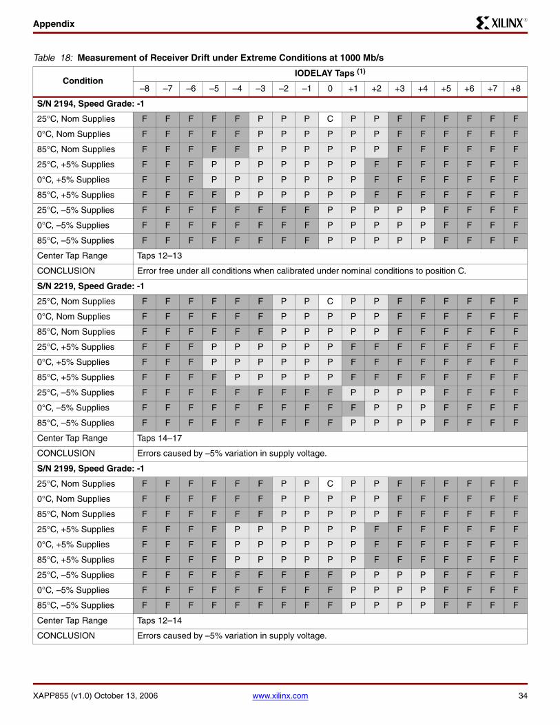
Appendix
XAPP855 (v10) October 13 2006 wwwxilinxcom 34
R
Table 18 Measurement of Receiver Drift under Extreme Conditions at 1000 Mbs
ConditionIODELAY Taps (1)
ndash8 ndash7 ndash6 ndash5 ndash4 ndash3 ndash2 ndash1 0 +1 +2 +3 +4 +5 +6 +7 +8
SN 2194 Speed Grade -1
25degC Nom Supplies F F F F F P P P C P P F F F F F F
0degC Nom Supplies F F F F F P P P P P P F F F F F F
85degC Nom Supplies F F F F F P P P P P P F F F F F F
25degC +5 Supplies F F F P P P P P P P F F F F F F F
0degC +5 Supplies F F F P P P P P P P F F F F F F F
85degC +5 Supplies F F F F P P P P P P F F F F F F F
25degC ndash5 Supplies F F F F F F F F P P P P P F F F F
0degC ndash5 Supplies F F F F F F F F P P P P P F F F F
85degC ndash5 Supplies F F F F F F F F P P P P P F F F F
Center Tap Range Taps 12ndash13
CONCLUSION Error free under all conditions when calibrated under nominal conditions to position C
SN 2219 Speed Grade -1
25degC Nom Supplies F F F F F F P P C P P F F F F F F
0degC Nom Supplies F F F F F F P P P P P F F F F F F
85degC Nom Supplies F F F F F F P P P P P F F F F F F
25degC +5 Supplies F F F P P P P P P F F F F F F F F
0degC +5 Supplies F F F P P P P P P F F F F F F F F
85degC +5 Supplies F F F F P P P P P F F F F F F F F
25degC ndash5 Supplies F F F F F F F F F P P P P F F F F
0degC ndash5 Supplies F F F F F F F F F F P P P F F F F
85degC ndash5 Supplies F F F F F F F F F P P P P F F F F
Center Tap Range Taps 14ndash17
CONCLUSION Errors caused by ndash5 variation in supply voltage
SN 2199 Speed Grade -1
25degC Nom Supplies F F F F F F P P C P P F F F F F F
0degC Nom Supplies F F F F F F P P P P P F F F F F F
85degC Nom Supplies F F F F F F P P P P P F F F F F F
25degC +5 Supplies F F F F P P P P P P F F F F F F F
0degC +5 Supplies F F F F P P P P P P F F F F F F F
85degC +5 Supplies F F F F P P P P P P F F F F F F F
25degC ndash5 Supplies F F F F F F F F F P P P P F F F F
0degC ndash5 Supplies F F F F F F F F F P P P P F F F F
85degC ndash5 Supplies F F F F F F F F F P P P P F F F F
Center Tap Range Taps 12ndash14
CONCLUSION Errors caused by ndash5 variation in supply voltage
Appendix
XAPP855 (v10) October 13 2006 wwwxilinxcom 35
R
SN 001 Speed Grade -2
25degC Nom Supplies F F F F F F P P C P P P F F F F F
0degC Nom Supplies F F F F F F P P P P P P F F F F F
85degC Nom Supplies F F F F F F P P P P P P F F F F F
25degC +5 Supplies F F F F P P P P P P F F F F F F F
0degC +5 Supplies F F F F P P P P P P F F F F F F F
85degC +5 Supplies F F F F P P P P P P P F F F F F F
25degC ndash5 Supplies F F F F F F F F F P P P P F F F F
0degC ndash5 Supplies F F F F F F F F F P P P P F F F F
85degC ndash5 Supplies F F F F F F F F F P P P P F F F F
Center Tap Range Taps 11ndash12
CONCLUSION Errors caused by ndash5 variation in supply voltage
SN 002 Speed Grade -2
25degC Nom Supplies F F F F F P P P C P P F F F F F F
0degC Nom Supplies F F F F F P P P P P P P F F F F F
85degC Nom Supplies F F F F F P P P P P P P F F F F F
25degC +5 Supplies F F F F P P P P P P F F F F F F F
0degC +5 Supplies F F F P P P P P P P F F F F F F F
85degC +5 Supplies F F F F P P P P P P P F F F F F F
25degC ndash5 Supplies F F F F F F F P P P P P P F F F F
0degC ndash5 Supplies F F F F F F F P P P P P P F F F F
85degC ndash5 Supplies F F F F F F F P P P P P P F F F F
Center Tap Range Taps 11ndash13
CONCLUSION Error free under all conditions when calibrated under nominal conditions to position C
SN 003 Speed Grade -2
25degC Nom Supplies F F F F F F P P C P P F F F F F F
0degC Nom Supplies F F F F F F P P P P P F F F F F F
85degC Nom Supplies F F F F F F P P P P P F F F F F F
25degC +5 Supplies F F F F P P P P P P F F F F F F F
0degC +5 Supplies F F F F P P P P P P F F F F F F F
85degC +5 Supplies F F F F P P P P P P F F F F F F F
25degC ndash5 Supplies F F F F F F F F F P P P P F F F F
0degC ndash5 Supplies F F F F F F F F F P P P P F F F F
85degC ndash5 Supplies F F F F F F F F F P P P P F F F F
Center Tap Range Taps 13ndash14
CONCLUSION Errors caused by ndash5 variation in supply voltage
Table 18 Measurement of Receiver Drift under Extreme Conditions at 1000 Mbs (Continued)
ConditionIODELAY Taps (1)
ndash8 ndash7 ndash6 ndash5 ndash4 ndash3 ndash2 ndash1 0 +1 +2 +3 +4 +5 +6 +7 +8
Appendix
XAPP855 (v10) October 13 2006 wwwxilinxcom 36
R
SN 004 Speed Grade -3
25degC Nom Supplies F F F F F P P P C P P P F F F F F
0degC Nom Supplies F F F F F P P P P P P P F F F F F
85degC Nom Supplies F F F F F P P P P P P P F F F F F
25degC +5 Supplies F F F P P P P P P P P F F F F F F
0degC +5 Supplies F F F P P P P P P P P F F F F F F
85degC +5 Supplies F F F F P P P P P P P P F F F F F
25degC ndash5 Supplies F F F F F F F P P P P P P F F F F
0degC ndash5 Supplies F F F F F F F P P P P P P F F F F
85degC ndash5 Supplies F F F F F F F P P P P P P P F F F
Center Tap Range Taps 9ndash10
CONCLUSION Error free under all conditions when calibrated under nominal conditions to position C
SN 005 Speed Grade -3
25degC Nom Supplies F F F F P P P P C P P P F F F F F
0degC Nom Supplies F F F F P P P P P P P P F F F F F
85degC Nom Supplies F F F F P P P P P P P P F F F F F
25degC +5 Supplies F F F P P P P P P P P F F F F F F
0degC +5 Supplies F F P P P P P P P P P F F F F F F
85degC +5 Supplies F F F P P P P P P P P F F F F F F
25degC ndash5 Supplies F F F F F F P P P P P P P P F F F
0degC ndash5 Supplies F F F F F F P P P P P P P P F F F
85degC ndash5 Supplies F F F F F F P P P P P P P F F F F
Center Tap Range Taps 11ndash12
CONCLUSION Error free under all conditions when calibrated under nominal conditions to position C
SN 006 Speed Grade -3
25degC Nom Supplies F F F F P P P P C P P P F F F F F
0degC Nom Supplies F F F F P P P P P P P P F F F F F
85degC Nom Supplies F F F F P P P P P P P P F F F F F
25degC +5 Supplies F F F P P P P P P P P F F F F F F
0degC +5 Supplies F F F P P P P P P P P F F F F F F
85degC +5 Supplies F F F P P P P P P P P F F F F F F
25degC ndash5 Supplies F F F F F F P P P P P P P F F F F
0degC ndash5 Supplies F F F F F F P P P P P P P F F F F
85degC ndash5 Supplies F F F F F F P P P P P P P F F F F
Center Tap Range Taps 9ndash10
CONCLUSION Error free under all conditions when calibrated under nominal conditions to position C
Notes 1 IODELAY taps where 0 is the reference tap determined by the bit align machine at nominal voltage and 25degC2 P = Error-free transmission F = Error in transmission C = IODELAY tap position selected by bit-align machine under nominal conditions at 25degC
Table 18 Measurement of Receiver Drift under Extreme Conditions at 1000 Mbs (Continued)
ConditionIODELAY Taps (1)
ndash8 ndash7 ndash6 ndash5 ndash4 ndash3 ndash2 ndash1 0 +1 +2 +3 +4 +5 +6 +7 +8
Appendix
XAPP855 (v10) October 13 2006 wwwxilinxcom 37
R
Table 19 Measurement of Receiver Drift under Extreme Conditions at 1100 Mbs
ConditionIODELAY Taps (1)
ndash8 ndash7 ndash6 ndash5 ndash4 ndash3 ndash2 ndash1 0 +1 +2 +3 +4 +5 +6 +7 +8
SN 2194 Speed Grade -1
25degC Nom Supplies F F F F F F P P C P P F F F F F F
0degC Nom Supplies F F F F F F P P P P P F F F F F F
85degC Nom Supplies F F F F F F P P P P P F F F F F F
25degC +5 Supplies F F F F P P P P P F F F F F F F F
0degC +5 Supplies F F F F P P P P P F F F F F F F F
85degC +5 Supplies F F F F P P P P P F F F F F F F F
25degC ndash5 Supplies F F F F F F F F F P P P F F F F F
0degC ndash5 Supplies F F F F F F F F F P P P F F F F F
85degC ndash5 Supplies F F F F F F F F F P P P F F F F F
Center Tap Range Taps 13ndash14
CONCLUSION Errors caused by ndash5 variation in supply voltage
SN 2219 Speed Grade -1
25degC Nom Supplies F F F F F F P P C P F F F F F F F
0degC Nom Supplies F F F F F F P P P P F F F F F F F
85degC Nom Supplies F F F F F F P P P P F F F F F F F
25degC +5 Supplies F F F F P P P P F F F F F F F F F
0degC +5 Supplies F F F F P P P P F F F F F F F F F
85degC +5 Supplies F F F F P P P P F F F F F F F F F
25degC ndash5 Supplies F F F F F F F F F F P P F F F F F
0degC ndash5 Supplies F F F F F F F F F F P P F F F F F
85degC ndash5 Supplies F F F F F F F F F P P P F F F F F
Center Tap Range Taps 6 15ndash17
CONCLUSION Errors caused by plusmn5 variation in supply voltage
SN 2199 Speed Grade -1
25degC Nom Supplies F F F F F F F P C P F F F F F F F
0degC Nom Supplies F F F F F F F P P P F F F F F F F
85degC Nom Supplies F F F F F F F P P P F F F F F F F
25degC +5 Supplies F F F F P P P P P F F F F F F F F
0degC +5 Supplies F F F F P P P P P F F F F F F F F
85degC +5 Supplies F F F F F P P P P F F F F F F F F
25degC ndash5 Supplies F F F F F F F F F F P P F F F F F
0degC ndash5 Supplies F F F F F F F F F F P P F F F F F
85degC ndash5 Supplies F F F F F F F F F F P P F F F F F
Center Tap Range Taps 13ndash15
CONCLUSION Errors caused by ndash5 variation in supply voltage
Appendix
XAPP855 (v10) October 13 2006 wwwxilinxcom 38
R
SN 001 Speed Grade -2
25degC Nom Supplies F F F F F F P P C P P F F F F F F
0degC Nom Supplies F F F F F F P P P P P F F F F F F
85degC Nom Supplies F F F F F F P P P P P F F F F F F
25degC +5 Supplies F F F F P P P P P F F F F F F F F
0degC +5 Supplies F F F F P P P P P F F F F F F F F
85degC +5 Supplies F F F F P P P P P F F F F F F F F
25degC ndash5 Supplies F F F F F F F F P P P P F F F F F
0degC ndash5 Supplies F F F F F F F F P P P P F F F F F
85degC ndash5 Supplies F F F F F F F F P P P P F F F F F
Center Tap Range Taps 12ndash13
CONCLUSION Error free under all conditions when calibrated under nominal conditions to position C
SN 002 Speed Grade -2
25degC Nom Supplies F F F F F P P P C P F F F F F F F
0degC Nom Supplies F F F F F P P P P P F F F F F F F
85degC Nom Supplies F F F F F F P P P P F F F F F F F
25degC +5 Supplies F F F F P P P P P F F F F F F F F
0degC +5 Supplies F F F P P P P P P F F F F F F F F
85degC +5 Supplies F F F F P P P P P F F F F F F F F
25degC ndash5 Supplies F F F F F F F F P P P P F F F F F
0degC ndash5 Supplies F F F F F F F F P P P P F F F F F
85degC ndash5 Supplies F F F F F F F F P P P P F F F F F
Center Tap Range Taps 13ndash14
CONCLUSION Error free under all conditions when calibrated under nominal conditions to position C
SN 003 Speed Grade -2
25degC Nom Supplies F F F F F F F P C P F F F F F F F
0degC Nom Supplies F F F F F F F P P P F F F F F F F
85degC Nom Supplies F F F F F F F P P P P F F F F F F
25degC +5 Supplies F F F F F P P P P F F F F F F F F
0degC +5 Supplies F F F F F P P P P F F F F F F F F
85degC +5 Supplies F F F F F P P P P F F F F F F F F
25degC ndash5 Supplies F F F F F F F F F F P P F F F F F
0degC ndash5 Supplies F F F F F F F F F F P P F F F F F
85degC ndash5 Supplies F F F F F F F F F P P P F F F F F
Center Tap Range Taps 14ndash16
CONCLUSION Errors caused by ndash5 variation in supply voltage
Table 19 Measurement of Receiver Drift under Extreme Conditions at 1100 Mbs (Continued)
ConditionIODELAY Taps (1)
ndash8 ndash7 ndash6 ndash5 ndash4 ndash3 ndash2 ndash1 0 +1 +2 +3 +4 +5 +6 +7 +8
Appendix
XAPP855 (v10) October 13 2006 wwwxilinxcom 39
R
SN 004 Speed Grade -3
25degC Nom Supplies F F F F F P P P C P P F F F F F F
0degC Nom Supplies F F F F F P P P P P P F F F F F F
85degC Nom Supplies F F F F F F P P P P P F F F F F F
25degC +5 Supplies F F F F P P P P P P F F F F F F F
0degC +5 Supplies F F F F P P P P P P F F F F F F F
85degC +5 Supplies F F F F P P P P P P F F F F F F F
25degC ndash5 Supplies F F F F F F F F P P P P F F F F F
0degC ndash5 Supplies F F F F F F F P P P P P F F F F F
85degC ndash5 Supplies F F F F F F F F P P P P P F F F F
Center Tap Range Taps 9ndash10
CONCLUSION Error free under all conditions when calibrated under nominal conditions to position C
SN 005 Speed Grade -3
25degC Nom Supplies F F F F F P P P C P P F F F F F F
0degC Nom Supplies F F F F F P P P P P P F F F F F F
85degC Nom Supplies F F F F F F P P P P P F F F F F F
25degC +5 Supplies F F F F P P P P P P F F F F F F F
0degC +5 Supplies F F F F P P P P P P F F F F F F F
85degC +5 Supplies F F F F P P P P P P F F F F F F F
25degC ndash5 Supplies F F F F F F F P P P P P P F F F F
0degC ndash5 Supplies F F F F F F F P P P P P P F F F F
85degC ndash5 Supplies F F F F F F F P P P P P P F F F F
Center Tap Range Taps 11ndash12
CONCLUSION Error free under all conditions when calibrated under nominal conditions to position C
SN 006 Speed Grade -3
25degC Nom Supplies F F F F F P P P C P P P F F F F F
0degC Nom Supplies F F F F F P P P P P P F F F F F F
85degC Nom Supplies F F F F F P P P P P P P F F F F F
25degC +5 Supplies F F F F P P P P P P P F F F F F F
0degC +5 Supplies F F F P P P P P P P F F F F F F F
85degC +5 Supplies F F F F P P P P P P P F F F F F F
25degC ndash5 Supplies F F F F F F P P P P P P P F F F F
0degC ndash5 Supplies F F F F F F P P P P P P P F F F F
85degC ndash5 Supplies F F F F F F F P P P P P P F F F F
Center Tap Range Taps 9ndash10
CONCLUSION Error free under all conditions when calibrated under nominal conditions to position C
Notes 1 IODELAY taps where 0 is the reference tap determined by the bit align machine at nominal voltage and 25degC2 P = Error-free transmission F = Error in transmission C = IODELAY tap position selected by bit-align machine under nominal conditions at 25degC
Table 19 Measurement of Receiver Drift under Extreme Conditions at 1100 Mbs (Continued)
ConditionIODELAY Taps (1)
ndash8 ndash7 ndash6 ndash5 ndash4 ndash3 ndash2 ndash1 0 +1 +2 +3 +4 +5 +6 +7 +8
Appendix
XAPP855 (v10) October 13 2006 wwwxilinxcom 40
R
Table 20 Measurement of Receiver Drift under Extreme Conditions at 1200 Mbs
ConditionIODELAY Taps (1)
ndash8 ndash7 ndash6 ndash5 ndash4 ndash3 ndash2 ndash1 0 +1 +2 +3 +4 +5 +6 +7 +8
SN 2194 Speed Grade -1
25degC Nom Supplies F F F F F F F P C F F F F F F F F
0degC Nom Supplies F F F F F F F P P F F F F F F F F
85degC Nom Supplies F F F F F F F P P F F F F F F F F
25degC +5 Supplies F F F F P P P P F F F F F F F F F
0degC +5 Supplies F F F F P P P P F F F F F F F F F
85degC +5 Supplies F F F F F P P P F F F F F F F F F
25degC ndash5 Supplies F F F F F F F F F P P F F F F F F
0degC ndash5 Supplies F F F F F F F F F F P F F F F F F
85degC ndash5 Supplies F F F F F F F F F P F F F F F F F
Center Tap Range Taps 13ndash15
CONCLUSION Errors caused by plusmn5 variation in supply voltage
SN 2219 Speed Grade -1
25degC Nom Supplies F F F F F F F F C F F F F F F F F
0degC Nom Supplies F F F F F F F P P F F F F F F F F
85degC Nom Supplies F F F F F F F F P F F F F F F F F
25degC +5 Supplies F F F F F P P P F F F F F F F F F
0degC +5 Supplies F F F F F P P P F F F F F F F F F
85degC +5 Supplies F F F F F F P P F F F F F F F F F
25degC ndash5 Supplies F F F F F F F F F F F F F F F F F
0degC ndash5 Supplies F F F F F F F F F F F F F F F F F
85degC ndash5 Supplies F F F F F F F F F F F F F F F F F
Center Tap Range Taps 6ndash7 16ndash17
CONCLUSION Errors caused by plusmn5 variation in supply voltage
SN 2199 Speed Grade -1
25degC Nom Supplies F F F F F F F P C F F F F F F F F
0degC Nom Supplies F F F F F F F P P F F F F F F F F
85degC Nom Supplies F F F F F F F F P F F F F F F F F
25degC +5 Supplies F F F F F P P P F F F F F F F F F
0degC +5 Supplies F F F F F P P P F F F F F F F F F
85degC +5 Supplies F F F F F P P P F F F F F F F F F
25degC ndash5 Supplies F F F F F F F F F F F F F F F F F
0degC ndash5 Supplies F F F F F F F F F F F F F F F F F
85degC ndash5 Supplies F F F F F F F F F F F F F F F F F
Center Tap Range Taps 13ndash15
CONCLUSION Errors caused by plusmn5 variation in supply voltage
Appendix
XAPP855 (v10) October 13 2006 wwwxilinxcom 41
R
SN 001 Speed Grade -2
25degC Nom Supplies F F F F F F F P C P F F F F F F F
0degC Nom Supplies F F F F F F F P P P F F F F F F F
85degC Nom Supplies F F F F F F F P P P F F F F F F F
25degC +5 Supplies F F F F F P P P P F F F F F F F F
0degC +5 Supplies F F F F P P P P P F F F F F F F F
85degC +5 Supplies F F F F F P P P P F F F F F F F F
25degC ndash5 Supplies F F F F F F F F F F P F F F F F F
0degC ndash5 Supplies F F F F F F F F F F P F F F F F F
85degC ndash5 Supplies F F F F F F F F F F P F F F F F F
Center Tap Range Taps 12ndash13
CONCLUSION Errors caused by ndash5 variation in supply voltage
SN 002 Speed Grade -2
25degC Nom Supplies F F F F F F P P C P F F F F F F F
0degC Nom Supplies F F F F F F P P P P F F F F F F F
85degC Nom Supplies F F F F F F F P P P F F F F F F F
25degC +5 Supplies F F F F P P P P F F F F F F F F F
0degC +5 Supplies F F F F P P P P F F F F F F F F F
85degC +5 Supplies F F F F F P P P F F F F F F F F F
25degC ndash5 Supplies F F F F F F F F P P P F F F F F F
0degC ndash5 Supplies F F F F F F F F P P P F F F F F F
85degC ndash5 Supplies F F F F F F F F F P P F F F F F F
Center Tap Range Taps 13ndash14
CONCLUSION Errors caused by plusmn5 variation in supply voltage
SN 003 Speed Grade -2
25degC Nom Supplies F F F F F F F P C F F F F F F F F
0degC Nom Supplies F F F F F F F P P F F F F F F F F
85degC Nom Supplies F F F F F F F F P F F F F F F F F
25degC +5 Supplies F F F F F P P P F F F F F F F F F
0degC +5 Supplies F F F F F P P P F F F F F F F F F
85degC +5 Supplies F F F F F F P P F F F F F F F F F
25degC ndash5 Supplies F F F F F F F F F F F F F F F F F
0degC ndash5 Supplies F F F F F F F F F F F F F F F F F
85degC ndash5 Supplies F F F F F F F F F F F F F F F F F
Center Tap Range Taps 14ndash15
CONCLUSION Errors caused by plusmn5 variation in supply voltage
Table 20 Measurement of Receiver Drift under Extreme Conditions at 1200 Mbs (Continued)
ConditionIODELAY Taps (1)
ndash8 ndash7 ndash6 ndash5 ndash4 ndash3 ndash2 ndash1 0 +1 +2 +3 +4 +5 +6 +7 +8
Appendix
XAPP855 (v10) October 13 2006 wwwxilinxcom 42
R
SN 004 Speed Grade -3
25degC Nom Supplies F F F F F F P P C P F F F F F F F
0degC Nom Supplies F F F F F P P P P P F F F F F F F
85degC Nom Supplies F F F F F F P P P P F F F F F F F
25degC +5 Supplies F F F F P P P P P F F F F F F F F
0degC +5 Supplies F F F F P P P P P F F F F F F F F
85degC +5 Supplies F F F F F P P P P F F F F F F F F
25degC ndash5 Supplies F F F F F F F F P P P F F F F F F
0degC ndash5 Supplies F F F F F F F F P P P F F F F F F
85degC ndash5 Supplies F F F F F F F F P P P F F F F F F
Center Tap Range Taps 9ndash11
CONCLUSION Error free under all conditions when calibrated under nominal conditions to position C
SN 005 Speed Grade -3
25degC Nom Supplies F F F F F P P P C P F F F F F F F
0degC Nom Supplies F F F F F P P P P P F F F F F F F
85degC Nom Supplies F F F F F F P P P P F F F F F F F
25degC +5 Supplies F F F F P P P P P F F F F F F F F
0degC +5 Supplies F F F P P P P P P F F F F F F F F
85degC +5 Supplies F F F F P P P P P F F F F F F F F
25degC ndash5 Supplies F F F F F F F P P P P P F F F F F
0degC ndash5 Supplies F F F F F F F P P P P P F F F F F
85degC ndash5 Supplies F F F F F F F F P P P F F F F F F
Center Tap Range Taps 11ndash13
CONCLUSION Error free under all conditions when calibrated under nominal conditions to position C
SN 006 Speed Grade -3
25degC Nom Supplies F F F F F P P P C P F F F F F F F
0degC Nom Supplies F F F F F P P P P P F F F F F F F
85degC Nom Supplies F F F F F P P P P P F F F F F F F
25degC +5 Supplies F F F P P P P P P F F F F F F F F
0degC +5 Supplies F F F P P P P P P F F F F F F F F
85degC +5 Supplies F F F F P P P P P F F F F F F F F
25degC ndash5 Supplies F F F F F F F P P P P F F F F F F
0degC ndash5 Supplies F F F F F F P P P P P F F F F F F
85degC ndash5 Supplies F F F F F F F P P P P F F F F F F
Center Tap Range Taps 10ndash11
CONCLUSION Error free under all conditions when calibrated under nominal conditions to position C
Notes 1 IODELAY taps where 0 is the reference tap determined by the bit align machine at nominal voltage and 25degC2 P = Error-free transmission F = Error in transmission C = IODELAY tap position selected by bit-align machine under nominal conditions at 25degC
Table 20 Measurement of Receiver Drift under Extreme Conditions at 1200 Mbs (Continued)
ConditionIODELAY Taps (1)
ndash8 ndash7 ndash6 ndash5 ndash4 ndash3 ndash2 ndash1 0 +1 +2 +3 +4 +5 +6 +7 +8
Revision History
XAPP855 (v10) October 13 2006 wwwxilinxcom 43
R
Revision History
The following table shows the revision history for this document
Date Version Revision
101306 10 Initial Xilinx release
- 16-Channel DDR LVDS Interface with Per-Channel Alignment
-
- Summary
- Introduction
-
- Figure 1 Full-Duplex 16-Channel DDR Link between a Virtex-5 Device and Another Device with a 16-Channel DDR Interface
- Figure 2 BERT Testbench for Hardware Verification of the DDR Interface
- Figure 3 Design Hierarchy of the Interface (TX and RX)
-
- DDR Transmitter
-
- Table 1 DDR_8TO1_16CHAN_TX Module Port Definitions
- Figure 4 MasterSlave OSERDES Pair for a Single Data Channel with 81 Serialization
- Figure 5 Block Diagram of TX Interface
- Table 2 DDR TX Interface Utilization Statistics
-
- Interface Clocking
-
- Figure 6 Global and Regional Clocking Schemes in Virtex-5 FPGAs
- Table 3 Comparison of Global and IO Clock Performance by Speed Grade
-
- DDR Receiver
-
- Table 4 DDR_8TO1_16CHAN_RX Module Port Definitions
- Figure 7 MasterSlave ISERDES Pair for a Single Data Channel with 18 Deserialization
- Figure 8 Block Diagram of RX Interface
- Table 5 DDR RX Interface Utilization Statistics
-
- Receiver Interface Dynamic Timing
-
- Inherent Timing
-
- Figure 9 Timing Components of RX Data and Clock Paths
- Figure 10 ISE Timing Analyzer Properties Used in this Document
- Table 6 Datapath Timing Definitions
- Table 7 Clock Path Timing Definitions
- Table 8 Datapath Delay Inventory for a -1 Speed Grade XC5VLX50T Device
- Table 9 Clock Path Delay Inventory for a -1 Speed Grade XC5VLX50T Device
- Figure 11 Timing Windows Show Uncertainty in ClockData Relationship as Calculated by Timing Analyzer
-
- Dynamic Timing and BIT_ALIGN_MACHINE
-
- Figure 12 Inherent Timing Windows Shown in Relation to Multiple Data Rates
- Figure 13 Dynamic Bit-Alignment Procedure in BIT_ALIGN_MACHINE
- Table 10 Word Alignment in the DDR Receiver
- Figure 14 FSM in the BIT_ALIGN_MACHINE Module
-
- Interface Timing Budget
-
- Interface Characterization
-
- Figure 15 Bit-Alignment Algorithm Performance
- Table 11 Tap Setting Range For Various Data Rates Measured on a -2 Device
- Table 12 Measurement of Receiver Drift under Extreme Conditions for Multiple Data Rates
- Pattern Dependence of Receiver Performance
-
- Table 13 Link Performance for Various Types of Data Measured on a -2 Device
-
- Resetting the Interface
-
- Figure 16 Recommended Interface Reset Timing
-
- Conclusion
-
- Table 14 Performance of 16-Channel DDR Interface
-
- Appendix
-
- Performance Characterization Data
-
- Table 15 Summary of Interface Characterization Results
- Table 16 Measurement of Receiver Drift under Extreme Conditions at 800 Mbs
- Table 17 Measurement of Receiver Drift under Extreme Conditions at 900 Mbs
- Table 18 Measurement of Receiver Drift under Extreme Conditions at 1000 Mbs
- Table 19 Measurement of Receiver Drift under Extreme Conditions at 1100 Mbs
- Table 20 Measurement of Receiver Drift under Extreme Conditions at 1200 Mbs
-
- Revision History
-
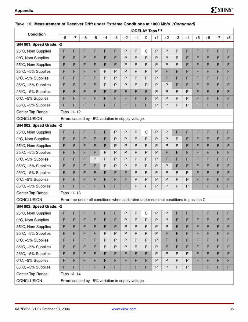
Appendix
XAPP855 (v10) October 13 2006 wwwxilinxcom 36
R
SN 004 Speed Grade -3
25degC Nom Supplies F F F F F P P P C P P P F F F F F
0degC Nom Supplies F F F F F P P P P P P P F F F F F
85degC Nom Supplies F F F F F P P P P P P P F F F F F
25degC +5 Supplies F F F P P P P P P P P F F F F F F
0degC +5 Supplies F F F P P P P P P P P F F F F F F
85degC +5 Supplies F F F F P P P P P P P P F F F F F
25degC ndash5 Supplies F F F F F F F P P P P P P F F F F
0degC ndash5 Supplies F F F F F F F P P P P P P F F F F
85degC ndash5 Supplies F F F F F F F P P P P P P P F F F
Center Tap Range Taps 9ndash10
CONCLUSION Error free under all conditions when calibrated under nominal conditions to position C
SN 005 Speed Grade -3
25degC Nom Supplies F F F F P P P P C P P P F F F F F
0degC Nom Supplies F F F F P P P P P P P P F F F F F
85degC Nom Supplies F F F F P P P P P P P P F F F F F
25degC +5 Supplies F F F P P P P P P P P F F F F F F
0degC +5 Supplies F F P P P P P P P P P F F F F F F
85degC +5 Supplies F F F P P P P P P P P F F F F F F
25degC ndash5 Supplies F F F F F F P P P P P P P P F F F
0degC ndash5 Supplies F F F F F F P P P P P P P P F F F
85degC ndash5 Supplies F F F F F F P P P P P P P F F F F
Center Tap Range Taps 11ndash12
CONCLUSION Error free under all conditions when calibrated under nominal conditions to position C
SN 006 Speed Grade -3
25degC Nom Supplies F F F F P P P P C P P P F F F F F
0degC Nom Supplies F F F F P P P P P P P P F F F F F
85degC Nom Supplies F F F F P P P P P P P P F F F F F
25degC +5 Supplies F F F P P P P P P P P F F F F F F
0degC +5 Supplies F F F P P P P P P P P F F F F F F
85degC +5 Supplies F F F P P P P P P P P F F F F F F
25degC ndash5 Supplies F F F F F F P P P P P P P F F F F
0degC ndash5 Supplies F F F F F F P P P P P P P F F F F
85degC ndash5 Supplies F F F F F F P P P P P P P F F F F
Center Tap Range Taps 9ndash10
CONCLUSION Error free under all conditions when calibrated under nominal conditions to position C
Notes 1 IODELAY taps where 0 is the reference tap determined by the bit align machine at nominal voltage and 25degC2 P = Error-free transmission F = Error in transmission C = IODELAY tap position selected by bit-align machine under nominal conditions at 25degC
Table 18 Measurement of Receiver Drift under Extreme Conditions at 1000 Mbs (Continued)
ConditionIODELAY Taps (1)
ndash8 ndash7 ndash6 ndash5 ndash4 ndash3 ndash2 ndash1 0 +1 +2 +3 +4 +5 +6 +7 +8
Appendix
XAPP855 (v10) October 13 2006 wwwxilinxcom 37
R
Table 19 Measurement of Receiver Drift under Extreme Conditions at 1100 Mbs
ConditionIODELAY Taps (1)
ndash8 ndash7 ndash6 ndash5 ndash4 ndash3 ndash2 ndash1 0 +1 +2 +3 +4 +5 +6 +7 +8
SN 2194 Speed Grade -1
25degC Nom Supplies F F F F F F P P C P P F F F F F F
0degC Nom Supplies F F F F F F P P P P P F F F F F F
85degC Nom Supplies F F F F F F P P P P P F F F F F F
25degC +5 Supplies F F F F P P P P P F F F F F F F F
0degC +5 Supplies F F F F P P P P P F F F F F F F F
85degC +5 Supplies F F F F P P P P P F F F F F F F F
25degC ndash5 Supplies F F F F F F F F F P P P F F F F F
0degC ndash5 Supplies F F F F F F F F F P P P F F F F F
85degC ndash5 Supplies F F F F F F F F F P P P F F F F F
Center Tap Range Taps 13ndash14
CONCLUSION Errors caused by ndash5 variation in supply voltage
SN 2219 Speed Grade -1
25degC Nom Supplies F F F F F F P P C P F F F F F F F
0degC Nom Supplies F F F F F F P P P P F F F F F F F
85degC Nom Supplies F F F F F F P P P P F F F F F F F
25degC +5 Supplies F F F F P P P P F F F F F F F F F
0degC +5 Supplies F F F F P P P P F F F F F F F F F
85degC +5 Supplies F F F F P P P P F F F F F F F F F
25degC ndash5 Supplies F F F F F F F F F F P P F F F F F
0degC ndash5 Supplies F F F F F F F F F F P P F F F F F
85degC ndash5 Supplies F F F F F F F F F P P P F F F F F
Center Tap Range Taps 6 15ndash17
CONCLUSION Errors caused by plusmn5 variation in supply voltage
SN 2199 Speed Grade -1
25degC Nom Supplies F F F F F F F P C P F F F F F F F
0degC Nom Supplies F F F F F F F P P P F F F F F F F
85degC Nom Supplies F F F F F F F P P P F F F F F F F
25degC +5 Supplies F F F F P P P P P F F F F F F F F
0degC +5 Supplies F F F F P P P P P F F F F F F F F
85degC +5 Supplies F F F F F P P P P F F F F F F F F
25degC ndash5 Supplies F F F F F F F F F F P P F F F F F
0degC ndash5 Supplies F F F F F F F F F F P P F F F F F
85degC ndash5 Supplies F F F F F F F F F F P P F F F F F
Center Tap Range Taps 13ndash15
CONCLUSION Errors caused by ndash5 variation in supply voltage
Appendix
XAPP855 (v10) October 13 2006 wwwxilinxcom 38
R
SN 001 Speed Grade -2
25degC Nom Supplies F F F F F F P P C P P F F F F F F
0degC Nom Supplies F F F F F F P P P P P F F F F F F
85degC Nom Supplies F F F F F F P P P P P F F F F F F
25degC +5 Supplies F F F F P P P P P F F F F F F F F
0degC +5 Supplies F F F F P P P P P F F F F F F F F
85degC +5 Supplies F F F F P P P P P F F F F F F F F
25degC ndash5 Supplies F F F F F F F F P P P P F F F F F
0degC ndash5 Supplies F F F F F F F F P P P P F F F F F
85degC ndash5 Supplies F F F F F F F F P P P P F F F F F
Center Tap Range Taps 12ndash13
CONCLUSION Error free under all conditions when calibrated under nominal conditions to position C
SN 002 Speed Grade -2
25degC Nom Supplies F F F F F P P P C P F F F F F F F
0degC Nom Supplies F F F F F P P P P P F F F F F F F
85degC Nom Supplies F F F F F F P P P P F F F F F F F
25degC +5 Supplies F F F F P P P P P F F F F F F F F
0degC +5 Supplies F F F P P P P P P F F F F F F F F
85degC +5 Supplies F F F F P P P P P F F F F F F F F
25degC ndash5 Supplies F F F F F F F F P P P P F F F F F
0degC ndash5 Supplies F F F F F F F F P P P P F F F F F
85degC ndash5 Supplies F F F F F F F F P P P P F F F F F
Center Tap Range Taps 13ndash14
CONCLUSION Error free under all conditions when calibrated under nominal conditions to position C
SN 003 Speed Grade -2
25degC Nom Supplies F F F F F F F P C P F F F F F F F
0degC Nom Supplies F F F F F F F P P P F F F F F F F
85degC Nom Supplies F F F F F F F P P P P F F F F F F
25degC +5 Supplies F F F F F P P P P F F F F F F F F
0degC +5 Supplies F F F F F P P P P F F F F F F F F
85degC +5 Supplies F F F F F P P P P F F F F F F F F
25degC ndash5 Supplies F F F F F F F F F F P P F F F F F
0degC ndash5 Supplies F F F F F F F F F F P P F F F F F
85degC ndash5 Supplies F F F F F F F F F P P P F F F F F
Center Tap Range Taps 14ndash16
CONCLUSION Errors caused by ndash5 variation in supply voltage
Table 19 Measurement of Receiver Drift under Extreme Conditions at 1100 Mbs (Continued)
ConditionIODELAY Taps (1)
ndash8 ndash7 ndash6 ndash5 ndash4 ndash3 ndash2 ndash1 0 +1 +2 +3 +4 +5 +6 +7 +8
Appendix
XAPP855 (v10) October 13 2006 wwwxilinxcom 39
R
SN 004 Speed Grade -3
25degC Nom Supplies F F F F F P P P C P P F F F F F F
0degC Nom Supplies F F F F F P P P P P P F F F F F F
85degC Nom Supplies F F F F F F P P P P P F F F F F F
25degC +5 Supplies F F F F P P P P P P F F F F F F F
0degC +5 Supplies F F F F P P P P P P F F F F F F F
85degC +5 Supplies F F F F P P P P P P F F F F F F F
25degC ndash5 Supplies F F F F F F F F P P P P F F F F F
0degC ndash5 Supplies F F F F F F F P P P P P F F F F F
85degC ndash5 Supplies F F F F F F F F P P P P P F F F F
Center Tap Range Taps 9ndash10
CONCLUSION Error free under all conditions when calibrated under nominal conditions to position C
SN 005 Speed Grade -3
25degC Nom Supplies F F F F F P P P C P P F F F F F F
0degC Nom Supplies F F F F F P P P P P P F F F F F F
85degC Nom Supplies F F F F F F P P P P P F F F F F F
25degC +5 Supplies F F F F P P P P P P F F F F F F F
0degC +5 Supplies F F F F P P P P P P F F F F F F F
85degC +5 Supplies F F F F P P P P P P F F F F F F F
25degC ndash5 Supplies F F F F F F F P P P P P P F F F F
0degC ndash5 Supplies F F F F F F F P P P P P P F F F F
85degC ndash5 Supplies F F F F F F F P P P P P P F F F F
Center Tap Range Taps 11ndash12
CONCLUSION Error free under all conditions when calibrated under nominal conditions to position C
SN 006 Speed Grade -3
25degC Nom Supplies F F F F F P P P C P P P F F F F F
0degC Nom Supplies F F F F F P P P P P P F F F F F F
85degC Nom Supplies F F F F F P P P P P P P F F F F F
25degC +5 Supplies F F F F P P P P P P P F F F F F F
0degC +5 Supplies F F F P P P P P P P F F F F F F F
85degC +5 Supplies F F F F P P P P P P P F F F F F F
25degC ndash5 Supplies F F F F F F P P P P P P P F F F F
0degC ndash5 Supplies F F F F F F P P P P P P P F F F F
85degC ndash5 Supplies F F F F F F F P P P P P P F F F F
Center Tap Range Taps 9ndash10
CONCLUSION Error free under all conditions when calibrated under nominal conditions to position C
Notes 1 IODELAY taps where 0 is the reference tap determined by the bit align machine at nominal voltage and 25degC2 P = Error-free transmission F = Error in transmission C = IODELAY tap position selected by bit-align machine under nominal conditions at 25degC
Table 19 Measurement of Receiver Drift under Extreme Conditions at 1100 Mbs (Continued)
ConditionIODELAY Taps (1)
ndash8 ndash7 ndash6 ndash5 ndash4 ndash3 ndash2 ndash1 0 +1 +2 +3 +4 +5 +6 +7 +8
Appendix
XAPP855 (v10) October 13 2006 wwwxilinxcom 40
R
Table 20 Measurement of Receiver Drift under Extreme Conditions at 1200 Mbs
ConditionIODELAY Taps (1)
ndash8 ndash7 ndash6 ndash5 ndash4 ndash3 ndash2 ndash1 0 +1 +2 +3 +4 +5 +6 +7 +8
SN 2194 Speed Grade -1
25degC Nom Supplies F F F F F F F P C F F F F F F F F
0degC Nom Supplies F F F F F F F P P F F F F F F F F
85degC Nom Supplies F F F F F F F P P F F F F F F F F
25degC +5 Supplies F F F F P P P P F F F F F F F F F
0degC +5 Supplies F F F F P P P P F F F F F F F F F
85degC +5 Supplies F F F F F P P P F F F F F F F F F
25degC ndash5 Supplies F F F F F F F F F P P F F F F F F
0degC ndash5 Supplies F F F F F F F F F F P F F F F F F
85degC ndash5 Supplies F F F F F F F F F P F F F F F F F
Center Tap Range Taps 13ndash15
CONCLUSION Errors caused by plusmn5 variation in supply voltage
SN 2219 Speed Grade -1
25degC Nom Supplies F F F F F F F F C F F F F F F F F
0degC Nom Supplies F F F F F F F P P F F F F F F F F
85degC Nom Supplies F F F F F F F F P F F F F F F F F
25degC +5 Supplies F F F F F P P P F F F F F F F F F
0degC +5 Supplies F F F F F P P P F F F F F F F F F
85degC +5 Supplies F F F F F F P P F F F F F F F F F
25degC ndash5 Supplies F F F F F F F F F F F F F F F F F
0degC ndash5 Supplies F F F F F F F F F F F F F F F F F
85degC ndash5 Supplies F F F F F F F F F F F F F F F F F
Center Tap Range Taps 6ndash7 16ndash17
CONCLUSION Errors caused by plusmn5 variation in supply voltage
SN 2199 Speed Grade -1
25degC Nom Supplies F F F F F F F P C F F F F F F F F
0degC Nom Supplies F F F F F F F P P F F F F F F F F
85degC Nom Supplies F F F F F F F F P F F F F F F F F
25degC +5 Supplies F F F F F P P P F F F F F F F F F
0degC +5 Supplies F F F F F P P P F F F F F F F F F
85degC +5 Supplies F F F F F P P P F F F F F F F F F
25degC ndash5 Supplies F F F F F F F F F F F F F F F F F
0degC ndash5 Supplies F F F F F F F F F F F F F F F F F
85degC ndash5 Supplies F F F F F F F F F F F F F F F F F
Center Tap Range Taps 13ndash15
CONCLUSION Errors caused by plusmn5 variation in supply voltage
Appendix
XAPP855 (v10) October 13 2006 wwwxilinxcom 41
R
SN 001 Speed Grade -2
25degC Nom Supplies F F F F F F F P C P F F F F F F F
0degC Nom Supplies F F F F F F F P P P F F F F F F F
85degC Nom Supplies F F F F F F F P P P F F F F F F F
25degC +5 Supplies F F F F F P P P P F F F F F F F F
0degC +5 Supplies F F F F P P P P P F F F F F F F F
85degC +5 Supplies F F F F F P P P P F F F F F F F F
25degC ndash5 Supplies F F F F F F F F F F P F F F F F F
0degC ndash5 Supplies F F F F F F F F F F P F F F F F F
85degC ndash5 Supplies F F F F F F F F F F P F F F F F F
Center Tap Range Taps 12ndash13
CONCLUSION Errors caused by ndash5 variation in supply voltage
SN 002 Speed Grade -2
25degC Nom Supplies F F F F F F P P C P F F F F F F F
0degC Nom Supplies F F F F F F P P P P F F F F F F F
85degC Nom Supplies F F F F F F F P P P F F F F F F F
25degC +5 Supplies F F F F P P P P F F F F F F F F F
0degC +5 Supplies F F F F P P P P F F F F F F F F F
85degC +5 Supplies F F F F F P P P F F F F F F F F F
25degC ndash5 Supplies F F F F F F F F P P P F F F F F F
0degC ndash5 Supplies F F F F F F F F P P P F F F F F F
85degC ndash5 Supplies F F F F F F F F F P P F F F F F F
Center Tap Range Taps 13ndash14
CONCLUSION Errors caused by plusmn5 variation in supply voltage
SN 003 Speed Grade -2
25degC Nom Supplies F F F F F F F P C F F F F F F F F
0degC Nom Supplies F F F F F F F P P F F F F F F F F
85degC Nom Supplies F F F F F F F F P F F F F F F F F
25degC +5 Supplies F F F F F P P P F F F F F F F F F
0degC +5 Supplies F F F F F P P P F F F F F F F F F
85degC +5 Supplies F F F F F F P P F F F F F F F F F
25degC ndash5 Supplies F F F F F F F F F F F F F F F F F
0degC ndash5 Supplies F F F F F F F F F F F F F F F F F
85degC ndash5 Supplies F F F F F F F F F F F F F F F F F
Center Tap Range Taps 14ndash15
CONCLUSION Errors caused by plusmn5 variation in supply voltage
Table 20 Measurement of Receiver Drift under Extreme Conditions at 1200 Mbs (Continued)
ConditionIODELAY Taps (1)
ndash8 ndash7 ndash6 ndash5 ndash4 ndash3 ndash2 ndash1 0 +1 +2 +3 +4 +5 +6 +7 +8
Appendix
XAPP855 (v10) October 13 2006 wwwxilinxcom 42
R
SN 004 Speed Grade -3
25degC Nom Supplies F F F F F F P P C P F F F F F F F
0degC Nom Supplies F F F F F P P P P P F F F F F F F
85degC Nom Supplies F F F F F F P P P P F F F F F F F
25degC +5 Supplies F F F F P P P P P F F F F F F F F
0degC +5 Supplies F F F F P P P P P F F F F F F F F
85degC +5 Supplies F F F F F P P P P F F F F F F F F
25degC ndash5 Supplies F F F F F F F F P P P F F F F F F
0degC ndash5 Supplies F F F F F F F F P P P F F F F F F
85degC ndash5 Supplies F F F F F F F F P P P F F F F F F
Center Tap Range Taps 9ndash11
CONCLUSION Error free under all conditions when calibrated under nominal conditions to position C
SN 005 Speed Grade -3
25degC Nom Supplies F F F F F P P P C P F F F F F F F
0degC Nom Supplies F F F F F P P P P P F F F F F F F
85degC Nom Supplies F F F F F F P P P P F F F F F F F
25degC +5 Supplies F F F F P P P P P F F F F F F F F
0degC +5 Supplies F F F P P P P P P F F F F F F F F
85degC +5 Supplies F F F F P P P P P F F F F F F F F
25degC ndash5 Supplies F F F F F F F P P P P P F F F F F
0degC ndash5 Supplies F F F F F F F P P P P P F F F F F
85degC ndash5 Supplies F F F F F F F F P P P F F F F F F
Center Tap Range Taps 11ndash13
CONCLUSION Error free under all conditions when calibrated under nominal conditions to position C
SN 006 Speed Grade -3
25degC Nom Supplies F F F F F P P P C P F F F F F F F
0degC Nom Supplies F F F F F P P P P P F F F F F F F
85degC Nom Supplies F F F F F P P P P P F F F F F F F
25degC +5 Supplies F F F P P P P P P F F F F F F F F
0degC +5 Supplies F F F P P P P P P F F F F F F F F
85degC +5 Supplies F F F F P P P P P F F F F F F F F
25degC ndash5 Supplies F F F F F F F P P P P F F F F F F
0degC ndash5 Supplies F F F F F F P P P P P F F F F F F
85degC ndash5 Supplies F F F F F F F P P P P F F F F F F
Center Tap Range Taps 10ndash11
CONCLUSION Error free under all conditions when calibrated under nominal conditions to position C
Notes 1 IODELAY taps where 0 is the reference tap determined by the bit align machine at nominal voltage and 25degC2 P = Error-free transmission F = Error in transmission C = IODELAY tap position selected by bit-align machine under nominal conditions at 25degC
Table 20 Measurement of Receiver Drift under Extreme Conditions at 1200 Mbs (Continued)
ConditionIODELAY Taps (1)
ndash8 ndash7 ndash6 ndash5 ndash4 ndash3 ndash2 ndash1 0 +1 +2 +3 +4 +5 +6 +7 +8
Revision History
XAPP855 (v10) October 13 2006 wwwxilinxcom 43
R
Revision History
The following table shows the revision history for this document
Date Version Revision
101306 10 Initial Xilinx release
- 16-Channel DDR LVDS Interface with Per-Channel Alignment
-
- Summary
- Introduction
-
- Figure 1 Full-Duplex 16-Channel DDR Link between a Virtex-5 Device and Another Device with a 16-Channel DDR Interface
- Figure 2 BERT Testbench for Hardware Verification of the DDR Interface
- Figure 3 Design Hierarchy of the Interface (TX and RX)
-
- DDR Transmitter
-
- Table 1 DDR_8TO1_16CHAN_TX Module Port Definitions
- Figure 4 MasterSlave OSERDES Pair for a Single Data Channel with 81 Serialization
- Figure 5 Block Diagram of TX Interface
- Table 2 DDR TX Interface Utilization Statistics
-
- Interface Clocking
-
- Figure 6 Global and Regional Clocking Schemes in Virtex-5 FPGAs
- Table 3 Comparison of Global and IO Clock Performance by Speed Grade
-
- DDR Receiver
-
- Table 4 DDR_8TO1_16CHAN_RX Module Port Definitions
- Figure 7 MasterSlave ISERDES Pair for a Single Data Channel with 18 Deserialization
- Figure 8 Block Diagram of RX Interface
- Table 5 DDR RX Interface Utilization Statistics
-
- Receiver Interface Dynamic Timing
-
- Inherent Timing
-
- Figure 9 Timing Components of RX Data and Clock Paths
- Figure 10 ISE Timing Analyzer Properties Used in this Document
- Table 6 Datapath Timing Definitions
- Table 7 Clock Path Timing Definitions
- Table 8 Datapath Delay Inventory for a -1 Speed Grade XC5VLX50T Device
- Table 9 Clock Path Delay Inventory for a -1 Speed Grade XC5VLX50T Device
- Figure 11 Timing Windows Show Uncertainty in ClockData Relationship as Calculated by Timing Analyzer
-
- Dynamic Timing and BIT_ALIGN_MACHINE
-
- Figure 12 Inherent Timing Windows Shown in Relation to Multiple Data Rates
- Figure 13 Dynamic Bit-Alignment Procedure in BIT_ALIGN_MACHINE
- Table 10 Word Alignment in the DDR Receiver
- Figure 14 FSM in the BIT_ALIGN_MACHINE Module
-
- Interface Timing Budget
-
- Interface Characterization
-
- Figure 15 Bit-Alignment Algorithm Performance
- Table 11 Tap Setting Range For Various Data Rates Measured on a -2 Device
- Table 12 Measurement of Receiver Drift under Extreme Conditions for Multiple Data Rates
- Pattern Dependence of Receiver Performance
-
- Table 13 Link Performance for Various Types of Data Measured on a -2 Device
-
- Resetting the Interface
-
- Figure 16 Recommended Interface Reset Timing
-
- Conclusion
-
- Table 14 Performance of 16-Channel DDR Interface
-
- Appendix
-
- Performance Characterization Data
-
- Table 15 Summary of Interface Characterization Results
- Table 16 Measurement of Receiver Drift under Extreme Conditions at 800 Mbs
- Table 17 Measurement of Receiver Drift under Extreme Conditions at 900 Mbs
- Table 18 Measurement of Receiver Drift under Extreme Conditions at 1000 Mbs
- Table 19 Measurement of Receiver Drift under Extreme Conditions at 1100 Mbs
- Table 20 Measurement of Receiver Drift under Extreme Conditions at 1200 Mbs
-
- Revision History
-
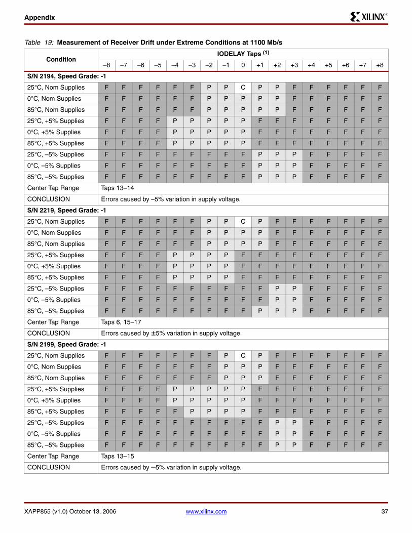
Appendix
XAPP855 (v10) October 13 2006 wwwxilinxcom 37
R
Table 19 Measurement of Receiver Drift under Extreme Conditions at 1100 Mbs
ConditionIODELAY Taps (1)
ndash8 ndash7 ndash6 ndash5 ndash4 ndash3 ndash2 ndash1 0 +1 +2 +3 +4 +5 +6 +7 +8
SN 2194 Speed Grade -1
25degC Nom Supplies F F F F F F P P C P P F F F F F F
0degC Nom Supplies F F F F F F P P P P P F F F F F F
85degC Nom Supplies F F F F F F P P P P P F F F F F F
25degC +5 Supplies F F F F P P P P P F F F F F F F F
0degC +5 Supplies F F F F P P P P P F F F F F F F F
85degC +5 Supplies F F F F P P P P P F F F F F F F F
25degC ndash5 Supplies F F F F F F F F F P P P F F F F F
0degC ndash5 Supplies F F F F F F F F F P P P F F F F F
85degC ndash5 Supplies F F F F F F F F F P P P F F F F F
Center Tap Range Taps 13ndash14
CONCLUSION Errors caused by ndash5 variation in supply voltage
SN 2219 Speed Grade -1
25degC Nom Supplies F F F F F F P P C P F F F F F F F
0degC Nom Supplies F F F F F F P P P P F F F F F F F
85degC Nom Supplies F F F F F F P P P P F F F F F F F
25degC +5 Supplies F F F F P P P P F F F F F F F F F
0degC +5 Supplies F F F F P P P P F F F F F F F F F
85degC +5 Supplies F F F F P P P P F F F F F F F F F
25degC ndash5 Supplies F F F F F F F F F F P P F F F F F
0degC ndash5 Supplies F F F F F F F F F F P P F F F F F
85degC ndash5 Supplies F F F F F F F F F P P P F F F F F
Center Tap Range Taps 6 15ndash17
CONCLUSION Errors caused by plusmn5 variation in supply voltage
SN 2199 Speed Grade -1
25degC Nom Supplies F F F F F F F P C P F F F F F F F
0degC Nom Supplies F F F F F F F P P P F F F F F F F
85degC Nom Supplies F F F F F F F P P P F F F F F F F
25degC +5 Supplies F F F F P P P P P F F F F F F F F
0degC +5 Supplies F F F F P P P P P F F F F F F F F
85degC +5 Supplies F F F F F P P P P F F F F F F F F
25degC ndash5 Supplies F F F F F F F F F F P P F F F F F
0degC ndash5 Supplies F F F F F F F F F F P P F F F F F
85degC ndash5 Supplies F F F F F F F F F F P P F F F F F
Center Tap Range Taps 13ndash15
CONCLUSION Errors caused by ndash5 variation in supply voltage
Appendix
XAPP855 (v10) October 13 2006 wwwxilinxcom 38
R
SN 001 Speed Grade -2
25degC Nom Supplies F F F F F F P P C P P F F F F F F
0degC Nom Supplies F F F F F F P P P P P F F F F F F
85degC Nom Supplies F F F F F F P P P P P F F F F F F
25degC +5 Supplies F F F F P P P P P F F F F F F F F
0degC +5 Supplies F F F F P P P P P F F F F F F F F
85degC +5 Supplies F F F F P P P P P F F F F F F F F
25degC ndash5 Supplies F F F F F F F F P P P P F F F F F
0degC ndash5 Supplies F F F F F F F F P P P P F F F F F
85degC ndash5 Supplies F F F F F F F F P P P P F F F F F
Center Tap Range Taps 12ndash13
CONCLUSION Error free under all conditions when calibrated under nominal conditions to position C
SN 002 Speed Grade -2
25degC Nom Supplies F F F F F P P P C P F F F F F F F
0degC Nom Supplies F F F F F P P P P P F F F F F F F
85degC Nom Supplies F F F F F F P P P P F F F F F F F
25degC +5 Supplies F F F F P P P P P F F F F F F F F
0degC +5 Supplies F F F P P P P P P F F F F F F F F
85degC +5 Supplies F F F F P P P P P F F F F F F F F
25degC ndash5 Supplies F F F F F F F F P P P P F F F F F
0degC ndash5 Supplies F F F F F F F F P P P P F F F F F
85degC ndash5 Supplies F F F F F F F F P P P P F F F F F
Center Tap Range Taps 13ndash14
CONCLUSION Error free under all conditions when calibrated under nominal conditions to position C
SN 003 Speed Grade -2
25degC Nom Supplies F F F F F F F P C P F F F F F F F
0degC Nom Supplies F F F F F F F P P P F F F F F F F
85degC Nom Supplies F F F F F F F P P P P F F F F F F
25degC +5 Supplies F F F F F P P P P F F F F F F F F
0degC +5 Supplies F F F F F P P P P F F F F F F F F
85degC +5 Supplies F F F F F P P P P F F F F F F F F
25degC ndash5 Supplies F F F F F F F F F F P P F F F F F
0degC ndash5 Supplies F F F F F F F F F F P P F F F F F
85degC ndash5 Supplies F F F F F F F F F P P P F F F F F
Center Tap Range Taps 14ndash16
CONCLUSION Errors caused by ndash5 variation in supply voltage
Table 19 Measurement of Receiver Drift under Extreme Conditions at 1100 Mbs (Continued)
ConditionIODELAY Taps (1)
ndash8 ndash7 ndash6 ndash5 ndash4 ndash3 ndash2 ndash1 0 +1 +2 +3 +4 +5 +6 +7 +8
Appendix
XAPP855 (v10) October 13 2006 wwwxilinxcom 39
R
SN 004 Speed Grade -3
25degC Nom Supplies F F F F F P P P C P P F F F F F F
0degC Nom Supplies F F F F F P P P P P P F F F F F F
85degC Nom Supplies F F F F F F P P P P P F F F F F F
25degC +5 Supplies F F F F P P P P P P F F F F F F F
0degC +5 Supplies F F F F P P P P P P F F F F F F F
85degC +5 Supplies F F F F P P P P P P F F F F F F F
25degC ndash5 Supplies F F F F F F F F P P P P F F F F F
0degC ndash5 Supplies F F F F F F F P P P P P F F F F F
85degC ndash5 Supplies F F F F F F F F P P P P P F F F F
Center Tap Range Taps 9ndash10
CONCLUSION Error free under all conditions when calibrated under nominal conditions to position C
SN 005 Speed Grade -3
25degC Nom Supplies F F F F F P P P C P P F F F F F F
0degC Nom Supplies F F F F F P P P P P P F F F F F F
85degC Nom Supplies F F F F F F P P P P P F F F F F F
25degC +5 Supplies F F F F P P P P P P F F F F F F F
0degC +5 Supplies F F F F P P P P P P F F F F F F F
85degC +5 Supplies F F F F P P P P P P F F F F F F F
25degC ndash5 Supplies F F F F F F F P P P P P P F F F F
0degC ndash5 Supplies F F F F F F F P P P P P P F F F F
85degC ndash5 Supplies F F F F F F F P P P P P P F F F F
Center Tap Range Taps 11ndash12
CONCLUSION Error free under all conditions when calibrated under nominal conditions to position C
SN 006 Speed Grade -3
25degC Nom Supplies F F F F F P P P C P P P F F F F F
0degC Nom Supplies F F F F F P P P P P P F F F F F F
85degC Nom Supplies F F F F F P P P P P P P F F F F F
25degC +5 Supplies F F F F P P P P P P P F F F F F F
0degC +5 Supplies F F F P P P P P P P F F F F F F F
85degC +5 Supplies F F F F P P P P P P P F F F F F F
25degC ndash5 Supplies F F F F F F P P P P P P P F F F F
0degC ndash5 Supplies F F F F F F P P P P P P P F F F F
85degC ndash5 Supplies F F F F F F F P P P P P P F F F F
Center Tap Range Taps 9ndash10
CONCLUSION Error free under all conditions when calibrated under nominal conditions to position C
Notes 1 IODELAY taps where 0 is the reference tap determined by the bit align machine at nominal voltage and 25degC2 P = Error-free transmission F = Error in transmission C = IODELAY tap position selected by bit-align machine under nominal conditions at 25degC
Table 19 Measurement of Receiver Drift under Extreme Conditions at 1100 Mbs (Continued)
ConditionIODELAY Taps (1)
ndash8 ndash7 ndash6 ndash5 ndash4 ndash3 ndash2 ndash1 0 +1 +2 +3 +4 +5 +6 +7 +8
Appendix
XAPP855 (v10) October 13 2006 wwwxilinxcom 40
R
Table 20 Measurement of Receiver Drift under Extreme Conditions at 1200 Mbs
ConditionIODELAY Taps (1)
ndash8 ndash7 ndash6 ndash5 ndash4 ndash3 ndash2 ndash1 0 +1 +2 +3 +4 +5 +6 +7 +8
SN 2194 Speed Grade -1
25degC Nom Supplies F F F F F F F P C F F F F F F F F
0degC Nom Supplies F F F F F F F P P F F F F F F F F
85degC Nom Supplies F F F F F F F P P F F F F F F F F
25degC +5 Supplies F F F F P P P P F F F F F F F F F
0degC +5 Supplies F F F F P P P P F F F F F F F F F
85degC +5 Supplies F F F F F P P P F F F F F F F F F
25degC ndash5 Supplies F F F F F F F F F P P F F F F F F
0degC ndash5 Supplies F F F F F F F F F F P F F F F F F
85degC ndash5 Supplies F F F F F F F F F P F F F F F F F
Center Tap Range Taps 13ndash15
CONCLUSION Errors caused by plusmn5 variation in supply voltage
SN 2219 Speed Grade -1
25degC Nom Supplies F F F F F F F F C F F F F F F F F
0degC Nom Supplies F F F F F F F P P F F F F F F F F
85degC Nom Supplies F F F F F F F F P F F F F F F F F
25degC +5 Supplies F F F F F P P P F F F F F F F F F
0degC +5 Supplies F F F F F P P P F F F F F F F F F
85degC +5 Supplies F F F F F F P P F F F F F F F F F
25degC ndash5 Supplies F F F F F F F F F F F F F F F F F
0degC ndash5 Supplies F F F F F F F F F F F F F F F F F
85degC ndash5 Supplies F F F F F F F F F F F F F F F F F
Center Tap Range Taps 6ndash7 16ndash17
CONCLUSION Errors caused by plusmn5 variation in supply voltage
SN 2199 Speed Grade -1
25degC Nom Supplies F F F F F F F P C F F F F F F F F
0degC Nom Supplies F F F F F F F P P F F F F F F F F
85degC Nom Supplies F F F F F F F F P F F F F F F F F
25degC +5 Supplies F F F F F P P P F F F F F F F F F
0degC +5 Supplies F F F F F P P P F F F F F F F F F
85degC +5 Supplies F F F F F P P P F F F F F F F F F
25degC ndash5 Supplies F F F F F F F F F F F F F F F F F
0degC ndash5 Supplies F F F F F F F F F F F F F F F F F
85degC ndash5 Supplies F F F F F F F F F F F F F F F F F
Center Tap Range Taps 13ndash15
CONCLUSION Errors caused by plusmn5 variation in supply voltage
Appendix
XAPP855 (v10) October 13 2006 wwwxilinxcom 41
R
SN 001 Speed Grade -2
25degC Nom Supplies F F F F F F F P C P F F F F F F F
0degC Nom Supplies F F F F F F F P P P F F F F F F F
85degC Nom Supplies F F F F F F F P P P F F F F F F F
25degC +5 Supplies F F F F F P P P P F F F F F F F F
0degC +5 Supplies F F F F P P P P P F F F F F F F F
85degC +5 Supplies F F F F F P P P P F F F F F F F F
25degC ndash5 Supplies F F F F F F F F F F P F F F F F F
0degC ndash5 Supplies F F F F F F F F F F P F F F F F F
85degC ndash5 Supplies F F F F F F F F F F P F F F F F F
Center Tap Range Taps 12ndash13
CONCLUSION Errors caused by ndash5 variation in supply voltage
SN 002 Speed Grade -2
25degC Nom Supplies F F F F F F P P C P F F F F F F F
0degC Nom Supplies F F F F F F P P P P F F F F F F F
85degC Nom Supplies F F F F F F F P P P F F F F F F F
25degC +5 Supplies F F F F P P P P F F F F F F F F F
0degC +5 Supplies F F F F P P P P F F F F F F F F F
85degC +5 Supplies F F F F F P P P F F F F F F F F F
25degC ndash5 Supplies F F F F F F F F P P P F F F F F F
0degC ndash5 Supplies F F F F F F F F P P P F F F F F F
85degC ndash5 Supplies F F F F F F F F F P P F F F F F F
Center Tap Range Taps 13ndash14
CONCLUSION Errors caused by plusmn5 variation in supply voltage
SN 003 Speed Grade -2
25degC Nom Supplies F F F F F F F P C F F F F F F F F
0degC Nom Supplies F F F F F F F P P F F F F F F F F
85degC Nom Supplies F F F F F F F F P F F F F F F F F
25degC +5 Supplies F F F F F P P P F F F F F F F F F
0degC +5 Supplies F F F F F P P P F F F F F F F F F
85degC +5 Supplies F F F F F F P P F F F F F F F F F
25degC ndash5 Supplies F F F F F F F F F F F F F F F F F
0degC ndash5 Supplies F F F F F F F F F F F F F F F F F
85degC ndash5 Supplies F F F F F F F F F F F F F F F F F
Center Tap Range Taps 14ndash15
CONCLUSION Errors caused by plusmn5 variation in supply voltage
Table 20 Measurement of Receiver Drift under Extreme Conditions at 1200 Mbs (Continued)
ConditionIODELAY Taps (1)
ndash8 ndash7 ndash6 ndash5 ndash4 ndash3 ndash2 ndash1 0 +1 +2 +3 +4 +5 +6 +7 +8
Appendix
XAPP855 (v10) October 13 2006 wwwxilinxcom 42
R
SN 004 Speed Grade -3
25degC Nom Supplies F F F F F F P P C P F F F F F F F
0degC Nom Supplies F F F F F P P P P P F F F F F F F
85degC Nom Supplies F F F F F F P P P P F F F F F F F
25degC +5 Supplies F F F F P P P P P F F F F F F F F
0degC +5 Supplies F F F F P P P P P F F F F F F F F
85degC +5 Supplies F F F F F P P P P F F F F F F F F
25degC ndash5 Supplies F F F F F F F F P P P F F F F F F
0degC ndash5 Supplies F F F F F F F F P P P F F F F F F
85degC ndash5 Supplies F F F F F F F F P P P F F F F F F
Center Tap Range Taps 9ndash11
CONCLUSION Error free under all conditions when calibrated under nominal conditions to position C
SN 005 Speed Grade -3
25degC Nom Supplies F F F F F P P P C P F F F F F F F
0degC Nom Supplies F F F F F P P P P P F F F F F F F
85degC Nom Supplies F F F F F F P P P P F F F F F F F
25degC +5 Supplies F F F F P P P P P F F F F F F F F
0degC +5 Supplies F F F P P P P P P F F F F F F F F
85degC +5 Supplies F F F F P P P P P F F F F F F F F
25degC ndash5 Supplies F F F F F F F P P P P P F F F F F
0degC ndash5 Supplies F F F F F F F P P P P P F F F F F
85degC ndash5 Supplies F F F F F F F F P P P F F F F F F
Center Tap Range Taps 11ndash13
CONCLUSION Error free under all conditions when calibrated under nominal conditions to position C
SN 006 Speed Grade -3
25degC Nom Supplies F F F F F P P P C P F F F F F F F
0degC Nom Supplies F F F F F P P P P P F F F F F F F
85degC Nom Supplies F F F F F P P P P P F F F F F F F
25degC +5 Supplies F F F P P P P P P F F F F F F F F
0degC +5 Supplies F F F P P P P P P F F F F F F F F
85degC +5 Supplies F F F F P P P P P F F F F F F F F
25degC ndash5 Supplies F F F F F F F P P P P F F F F F F
0degC ndash5 Supplies F F F F F F P P P P P F F F F F F
85degC ndash5 Supplies F F F F F F F P P P P F F F F F F
Center Tap Range Taps 10ndash11
CONCLUSION Error free under all conditions when calibrated under nominal conditions to position C
Notes 1 IODELAY taps where 0 is the reference tap determined by the bit align machine at nominal voltage and 25degC2 P = Error-free transmission F = Error in transmission C = IODELAY tap position selected by bit-align machine under nominal conditions at 25degC
Table 20 Measurement of Receiver Drift under Extreme Conditions at 1200 Mbs (Continued)
ConditionIODELAY Taps (1)
ndash8 ndash7 ndash6 ndash5 ndash4 ndash3 ndash2 ndash1 0 +1 +2 +3 +4 +5 +6 +7 +8
Revision History
XAPP855 (v10) October 13 2006 wwwxilinxcom 43
R
Revision History
The following table shows the revision history for this document
Date Version Revision
101306 10 Initial Xilinx release
- 16-Channel DDR LVDS Interface with Per-Channel Alignment
-
- Summary
- Introduction
-
- Figure 1 Full-Duplex 16-Channel DDR Link between a Virtex-5 Device and Another Device with a 16-Channel DDR Interface
- Figure 2 BERT Testbench for Hardware Verification of the DDR Interface
- Figure 3 Design Hierarchy of the Interface (TX and RX)
-
- DDR Transmitter
-
- Table 1 DDR_8TO1_16CHAN_TX Module Port Definitions
- Figure 4 MasterSlave OSERDES Pair for a Single Data Channel with 81 Serialization
- Figure 5 Block Diagram of TX Interface
- Table 2 DDR TX Interface Utilization Statistics
-
- Interface Clocking
-
- Figure 6 Global and Regional Clocking Schemes in Virtex-5 FPGAs
- Table 3 Comparison of Global and IO Clock Performance by Speed Grade
-
- DDR Receiver
-
- Table 4 DDR_8TO1_16CHAN_RX Module Port Definitions
- Figure 7 MasterSlave ISERDES Pair for a Single Data Channel with 18 Deserialization
- Figure 8 Block Diagram of RX Interface
- Table 5 DDR RX Interface Utilization Statistics
-
- Receiver Interface Dynamic Timing
-
- Inherent Timing
-
- Figure 9 Timing Components of RX Data and Clock Paths
- Figure 10 ISE Timing Analyzer Properties Used in this Document
- Table 6 Datapath Timing Definitions
- Table 7 Clock Path Timing Definitions
- Table 8 Datapath Delay Inventory for a -1 Speed Grade XC5VLX50T Device
- Table 9 Clock Path Delay Inventory for a -1 Speed Grade XC5VLX50T Device
- Figure 11 Timing Windows Show Uncertainty in ClockData Relationship as Calculated by Timing Analyzer
-
- Dynamic Timing and BIT_ALIGN_MACHINE
-
- Figure 12 Inherent Timing Windows Shown in Relation to Multiple Data Rates
- Figure 13 Dynamic Bit-Alignment Procedure in BIT_ALIGN_MACHINE
- Table 10 Word Alignment in the DDR Receiver
- Figure 14 FSM in the BIT_ALIGN_MACHINE Module
-
- Interface Timing Budget
-
- Interface Characterization
-
- Figure 15 Bit-Alignment Algorithm Performance
- Table 11 Tap Setting Range For Various Data Rates Measured on a -2 Device
- Table 12 Measurement of Receiver Drift under Extreme Conditions for Multiple Data Rates
- Pattern Dependence of Receiver Performance
-
- Table 13 Link Performance for Various Types of Data Measured on a -2 Device
-
- Resetting the Interface
-
- Figure 16 Recommended Interface Reset Timing
-
- Conclusion
-
- Table 14 Performance of 16-Channel DDR Interface
-
- Appendix
-
- Performance Characterization Data
-
- Table 15 Summary of Interface Characterization Results
- Table 16 Measurement of Receiver Drift under Extreme Conditions at 800 Mbs
- Table 17 Measurement of Receiver Drift under Extreme Conditions at 900 Mbs
- Table 18 Measurement of Receiver Drift under Extreme Conditions at 1000 Mbs
- Table 19 Measurement of Receiver Drift under Extreme Conditions at 1100 Mbs
- Table 20 Measurement of Receiver Drift under Extreme Conditions at 1200 Mbs
-
- Revision History
-
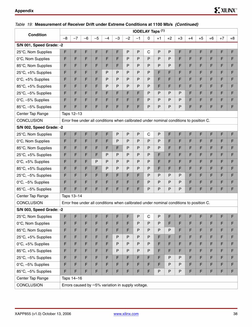
Appendix
XAPP855 (v10) October 13 2006 wwwxilinxcom 38
R
SN 001 Speed Grade -2
25degC Nom Supplies F F F F F F P P C P P F F F F F F
0degC Nom Supplies F F F F F F P P P P P F F F F F F
85degC Nom Supplies F F F F F F P P P P P F F F F F F
25degC +5 Supplies F F F F P P P P P F F F F F F F F
0degC +5 Supplies F F F F P P P P P F F F F F F F F
85degC +5 Supplies F F F F P P P P P F F F F F F F F
25degC ndash5 Supplies F F F F F F F F P P P P F F F F F
0degC ndash5 Supplies F F F F F F F F P P P P F F F F F
85degC ndash5 Supplies F F F F F F F F P P P P F F F F F
Center Tap Range Taps 12ndash13
CONCLUSION Error free under all conditions when calibrated under nominal conditions to position C
SN 002 Speed Grade -2
25degC Nom Supplies F F F F F P P P C P F F F F F F F
0degC Nom Supplies F F F F F P P P P P F F F F F F F
85degC Nom Supplies F F F F F F P P P P F F F F F F F
25degC +5 Supplies F F F F P P P P P F F F F F F F F
0degC +5 Supplies F F F P P P P P P F F F F F F F F
85degC +5 Supplies F F F F P P P P P F F F F F F F F
25degC ndash5 Supplies F F F F F F F F P P P P F F F F F
0degC ndash5 Supplies F F F F F F F F P P P P F F F F F
85degC ndash5 Supplies F F F F F F F F P P P P F F F F F
Center Tap Range Taps 13ndash14
CONCLUSION Error free under all conditions when calibrated under nominal conditions to position C
SN 003 Speed Grade -2
25degC Nom Supplies F F F F F F F P C P F F F F F F F
0degC Nom Supplies F F F F F F F P P P F F F F F F F
85degC Nom Supplies F F F F F F F P P P P F F F F F F
25degC +5 Supplies F F F F F P P P P F F F F F F F F
0degC +5 Supplies F F F F F P P P P F F F F F F F F
85degC +5 Supplies F F F F F P P P P F F F F F F F F
25degC ndash5 Supplies F F F F F F F F F F P P F F F F F
0degC ndash5 Supplies F F F F F F F F F F P P F F F F F
85degC ndash5 Supplies F F F F F F F F F P P P F F F F F
Center Tap Range Taps 14ndash16
CONCLUSION Errors caused by ndash5 variation in supply voltage
Table 19 Measurement of Receiver Drift under Extreme Conditions at 1100 Mbs (Continued)
ConditionIODELAY Taps (1)
ndash8 ndash7 ndash6 ndash5 ndash4 ndash3 ndash2 ndash1 0 +1 +2 +3 +4 +5 +6 +7 +8
Appendix
XAPP855 (v10) October 13 2006 wwwxilinxcom 39
R
SN 004 Speed Grade -3
25degC Nom Supplies F F F F F P P P C P P F F F F F F
0degC Nom Supplies F F F F F P P P P P P F F F F F F
85degC Nom Supplies F F F F F F P P P P P F F F F F F
25degC +5 Supplies F F F F P P P P P P F F F F F F F
0degC +5 Supplies F F F F P P P P P P F F F F F F F
85degC +5 Supplies F F F F P P P P P P F F F F F F F
25degC ndash5 Supplies F F F F F F F F P P P P F F F F F
0degC ndash5 Supplies F F F F F F F P P P P P F F F F F
85degC ndash5 Supplies F F F F F F F F P P P P P F F F F
Center Tap Range Taps 9ndash10
CONCLUSION Error free under all conditions when calibrated under nominal conditions to position C
SN 005 Speed Grade -3
25degC Nom Supplies F F F F F P P P C P P F F F F F F
0degC Nom Supplies F F F F F P P P P P P F F F F F F
85degC Nom Supplies F F F F F F P P P P P F F F F F F
25degC +5 Supplies F F F F P P P P P P F F F F F F F
0degC +5 Supplies F F F F P P P P P P F F F F F F F
85degC +5 Supplies F F F F P P P P P P F F F F F F F
25degC ndash5 Supplies F F F F F F F P P P P P P F F F F
0degC ndash5 Supplies F F F F F F F P P P P P P F F F F
85degC ndash5 Supplies F F F F F F F P P P P P P F F F F
Center Tap Range Taps 11ndash12
CONCLUSION Error free under all conditions when calibrated under nominal conditions to position C
SN 006 Speed Grade -3
25degC Nom Supplies F F F F F P P P C P P P F F F F F
0degC Nom Supplies F F F F F P P P P P P F F F F F F
85degC Nom Supplies F F F F F P P P P P P P F F F F F
25degC +5 Supplies F F F F P P P P P P P F F F F F F
0degC +5 Supplies F F F P P P P P P P F F F F F F F
85degC +5 Supplies F F F F P P P P P P P F F F F F F
25degC ndash5 Supplies F F F F F F P P P P P P P F F F F
0degC ndash5 Supplies F F F F F F P P P P P P P F F F F
85degC ndash5 Supplies F F F F F F F P P P P P P F F F F
Center Tap Range Taps 9ndash10
CONCLUSION Error free under all conditions when calibrated under nominal conditions to position C
Notes 1 IODELAY taps where 0 is the reference tap determined by the bit align machine at nominal voltage and 25degC2 P = Error-free transmission F = Error in transmission C = IODELAY tap position selected by bit-align machine under nominal conditions at 25degC
Table 19 Measurement of Receiver Drift under Extreme Conditions at 1100 Mbs (Continued)
ConditionIODELAY Taps (1)
ndash8 ndash7 ndash6 ndash5 ndash4 ndash3 ndash2 ndash1 0 +1 +2 +3 +4 +5 +6 +7 +8
Appendix
XAPP855 (v10) October 13 2006 wwwxilinxcom 40
R
Table 20 Measurement of Receiver Drift under Extreme Conditions at 1200 Mbs
ConditionIODELAY Taps (1)
ndash8 ndash7 ndash6 ndash5 ndash4 ndash3 ndash2 ndash1 0 +1 +2 +3 +4 +5 +6 +7 +8
SN 2194 Speed Grade -1
25degC Nom Supplies F F F F F F F P C F F F F F F F F
0degC Nom Supplies F F F F F F F P P F F F F F F F F
85degC Nom Supplies F F F F F F F P P F F F F F F F F
25degC +5 Supplies F F F F P P P P F F F F F F F F F
0degC +5 Supplies F F F F P P P P F F F F F F F F F
85degC +5 Supplies F F F F F P P P F F F F F F F F F
25degC ndash5 Supplies F F F F F F F F F P P F F F F F F
0degC ndash5 Supplies F F F F F F F F F F P F F F F F F
85degC ndash5 Supplies F F F F F F F F F P F F F F F F F
Center Tap Range Taps 13ndash15
CONCLUSION Errors caused by plusmn5 variation in supply voltage
SN 2219 Speed Grade -1
25degC Nom Supplies F F F F F F F F C F F F F F F F F
0degC Nom Supplies F F F F F F F P P F F F F F F F F
85degC Nom Supplies F F F F F F F F P F F F F F F F F
25degC +5 Supplies F F F F F P P P F F F F F F F F F
0degC +5 Supplies F F F F F P P P F F F F F F F F F
85degC +5 Supplies F F F F F F P P F F F F F F F F F
25degC ndash5 Supplies F F F F F F F F F F F F F F F F F
0degC ndash5 Supplies F F F F F F F F F F F F F F F F F
85degC ndash5 Supplies F F F F F F F F F F F F F F F F F
Center Tap Range Taps 6ndash7 16ndash17
CONCLUSION Errors caused by plusmn5 variation in supply voltage
SN 2199 Speed Grade -1
25degC Nom Supplies F F F F F F F P C F F F F F F F F
0degC Nom Supplies F F F F F F F P P F F F F F F F F
85degC Nom Supplies F F F F F F F F P F F F F F F F F
25degC +5 Supplies F F F F F P P P F F F F F F F F F
0degC +5 Supplies F F F F F P P P F F F F F F F F F
85degC +5 Supplies F F F F F P P P F F F F F F F F F
25degC ndash5 Supplies F F F F F F F F F F F F F F F F F
0degC ndash5 Supplies F F F F F F F F F F F F F F F F F
85degC ndash5 Supplies F F F F F F F F F F F F F F F F F
Center Tap Range Taps 13ndash15
CONCLUSION Errors caused by plusmn5 variation in supply voltage
Appendix
XAPP855 (v10) October 13 2006 wwwxilinxcom 41
R
SN 001 Speed Grade -2
25degC Nom Supplies F F F F F F F P C P F F F F F F F
0degC Nom Supplies F F F F F F F P P P F F F F F F F
85degC Nom Supplies F F F F F F F P P P F F F F F F F
25degC +5 Supplies F F F F F P P P P F F F F F F F F
0degC +5 Supplies F F F F P P P P P F F F F F F F F
85degC +5 Supplies F F F F F P P P P F F F F F F F F
25degC ndash5 Supplies F F F F F F F F F F P F F F F F F
0degC ndash5 Supplies F F F F F F F F F F P F F F F F F
85degC ndash5 Supplies F F F F F F F F F F P F F F F F F
Center Tap Range Taps 12ndash13
CONCLUSION Errors caused by ndash5 variation in supply voltage
SN 002 Speed Grade -2
25degC Nom Supplies F F F F F F P P C P F F F F F F F
0degC Nom Supplies F F F F F F P P P P F F F F F F F
85degC Nom Supplies F F F F F F F P P P F F F F F F F
25degC +5 Supplies F F F F P P P P F F F F F F F F F
0degC +5 Supplies F F F F P P P P F F F F F F F F F
85degC +5 Supplies F F F F F P P P F F F F F F F F F
25degC ndash5 Supplies F F F F F F F F P P P F F F F F F
0degC ndash5 Supplies F F F F F F F F P P P F F F F F F
85degC ndash5 Supplies F F F F F F F F F P P F F F F F F
Center Tap Range Taps 13ndash14
CONCLUSION Errors caused by plusmn5 variation in supply voltage
SN 003 Speed Grade -2
25degC Nom Supplies F F F F F F F P C F F F F F F F F
0degC Nom Supplies F F F F F F F P P F F F F F F F F
85degC Nom Supplies F F F F F F F F P F F F F F F F F
25degC +5 Supplies F F F F F P P P F F F F F F F F F
0degC +5 Supplies F F F F F P P P F F F F F F F F F
85degC +5 Supplies F F F F F F P P F F F F F F F F F
25degC ndash5 Supplies F F F F F F F F F F F F F F F F F
0degC ndash5 Supplies F F F F F F F F F F F F F F F F F
85degC ndash5 Supplies F F F F F F F F F F F F F F F F F
Center Tap Range Taps 14ndash15
CONCLUSION Errors caused by plusmn5 variation in supply voltage
Table 20 Measurement of Receiver Drift under Extreme Conditions at 1200 Mbs (Continued)
ConditionIODELAY Taps (1)
ndash8 ndash7 ndash6 ndash5 ndash4 ndash3 ndash2 ndash1 0 +1 +2 +3 +4 +5 +6 +7 +8
Appendix
XAPP855 (v10) October 13 2006 wwwxilinxcom 42
R
SN 004 Speed Grade -3
25degC Nom Supplies F F F F F F P P C P F F F F F F F
0degC Nom Supplies F F F F F P P P P P F F F F F F F
85degC Nom Supplies F F F F F F P P P P F F F F F F F
25degC +5 Supplies F F F F P P P P P F F F F F F F F
0degC +5 Supplies F F F F P P P P P F F F F F F F F
85degC +5 Supplies F F F F F P P P P F F F F F F F F
25degC ndash5 Supplies F F F F F F F F P P P F F F F F F
0degC ndash5 Supplies F F F F F F F F P P P F F F F F F
85degC ndash5 Supplies F F F F F F F F P P P F F F F F F
Center Tap Range Taps 9ndash11
CONCLUSION Error free under all conditions when calibrated under nominal conditions to position C
SN 005 Speed Grade -3
25degC Nom Supplies F F F F F P P P C P F F F F F F F
0degC Nom Supplies F F F F F P P P P P F F F F F F F
85degC Nom Supplies F F F F F F P P P P F F F F F F F
25degC +5 Supplies F F F F P P P P P F F F F F F F F
0degC +5 Supplies F F F P P P P P P F F F F F F F F
85degC +5 Supplies F F F F P P P P P F F F F F F F F
25degC ndash5 Supplies F F F F F F F P P P P P F F F F F
0degC ndash5 Supplies F F F F F F F P P P P P F F F F F
85degC ndash5 Supplies F F F F F F F F P P P F F F F F F
Center Tap Range Taps 11ndash13
CONCLUSION Error free under all conditions when calibrated under nominal conditions to position C
SN 006 Speed Grade -3
25degC Nom Supplies F F F F F P P P C P F F F F F F F
0degC Nom Supplies F F F F F P P P P P F F F F F F F
85degC Nom Supplies F F F F F P P P P P F F F F F F F
25degC +5 Supplies F F F P P P P P P F F F F F F F F
0degC +5 Supplies F F F P P P P P P F F F F F F F F
85degC +5 Supplies F F F F P P P P P F F F F F F F F
25degC ndash5 Supplies F F F F F F F P P P P F F F F F F
0degC ndash5 Supplies F F F F F F P P P P P F F F F F F
85degC ndash5 Supplies F F F F F F F P P P P F F F F F F
Center Tap Range Taps 10ndash11
CONCLUSION Error free under all conditions when calibrated under nominal conditions to position C
Notes 1 IODELAY taps where 0 is the reference tap determined by the bit align machine at nominal voltage and 25degC2 P = Error-free transmission F = Error in transmission C = IODELAY tap position selected by bit-align machine under nominal conditions at 25degC
Table 20 Measurement of Receiver Drift under Extreme Conditions at 1200 Mbs (Continued)
ConditionIODELAY Taps (1)
ndash8 ndash7 ndash6 ndash5 ndash4 ndash3 ndash2 ndash1 0 +1 +2 +3 +4 +5 +6 +7 +8
Revision History
XAPP855 (v10) October 13 2006 wwwxilinxcom 43
R
Revision History
The following table shows the revision history for this document
Date Version Revision
101306 10 Initial Xilinx release
- 16-Channel DDR LVDS Interface with Per-Channel Alignment
-
- Summary
- Introduction
-
- Figure 1 Full-Duplex 16-Channel DDR Link between a Virtex-5 Device and Another Device with a 16-Channel DDR Interface
- Figure 2 BERT Testbench for Hardware Verification of the DDR Interface
- Figure 3 Design Hierarchy of the Interface (TX and RX)
-
- DDR Transmitter
-
- Table 1 DDR_8TO1_16CHAN_TX Module Port Definitions
- Figure 4 MasterSlave OSERDES Pair for a Single Data Channel with 81 Serialization
- Figure 5 Block Diagram of TX Interface
- Table 2 DDR TX Interface Utilization Statistics
-
- Interface Clocking
-
- Figure 6 Global and Regional Clocking Schemes in Virtex-5 FPGAs
- Table 3 Comparison of Global and IO Clock Performance by Speed Grade
-
- DDR Receiver
-
- Table 4 DDR_8TO1_16CHAN_RX Module Port Definitions
- Figure 7 MasterSlave ISERDES Pair for a Single Data Channel with 18 Deserialization
- Figure 8 Block Diagram of RX Interface
- Table 5 DDR RX Interface Utilization Statistics
-
- Receiver Interface Dynamic Timing
-
- Inherent Timing
-
- Figure 9 Timing Components of RX Data and Clock Paths
- Figure 10 ISE Timing Analyzer Properties Used in this Document
- Table 6 Datapath Timing Definitions
- Table 7 Clock Path Timing Definitions
- Table 8 Datapath Delay Inventory for a -1 Speed Grade XC5VLX50T Device
- Table 9 Clock Path Delay Inventory for a -1 Speed Grade XC5VLX50T Device
- Figure 11 Timing Windows Show Uncertainty in ClockData Relationship as Calculated by Timing Analyzer
-
- Dynamic Timing and BIT_ALIGN_MACHINE
-
- Figure 12 Inherent Timing Windows Shown in Relation to Multiple Data Rates
- Figure 13 Dynamic Bit-Alignment Procedure in BIT_ALIGN_MACHINE
- Table 10 Word Alignment in the DDR Receiver
- Figure 14 FSM in the BIT_ALIGN_MACHINE Module
-
- Interface Timing Budget
-
- Interface Characterization
-
- Figure 15 Bit-Alignment Algorithm Performance
- Table 11 Tap Setting Range For Various Data Rates Measured on a -2 Device
- Table 12 Measurement of Receiver Drift under Extreme Conditions for Multiple Data Rates
- Pattern Dependence of Receiver Performance
-
- Table 13 Link Performance for Various Types of Data Measured on a -2 Device
-
- Resetting the Interface
-
- Figure 16 Recommended Interface Reset Timing
-
- Conclusion
-
- Table 14 Performance of 16-Channel DDR Interface
-
- Appendix
-
- Performance Characterization Data
-
- Table 15 Summary of Interface Characterization Results
- Table 16 Measurement of Receiver Drift under Extreme Conditions at 800 Mbs
- Table 17 Measurement of Receiver Drift under Extreme Conditions at 900 Mbs
- Table 18 Measurement of Receiver Drift under Extreme Conditions at 1000 Mbs
- Table 19 Measurement of Receiver Drift under Extreme Conditions at 1100 Mbs
- Table 20 Measurement of Receiver Drift under Extreme Conditions at 1200 Mbs
-
- Revision History
-
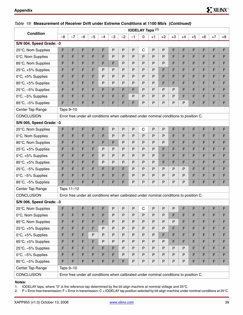
Appendix
XAPP855 (v10) October 13 2006 wwwxilinxcom 39
R
SN 004 Speed Grade -3
25degC Nom Supplies F F F F F P P P C P P F F F F F F
0degC Nom Supplies F F F F F P P P P P P F F F F F F
85degC Nom Supplies F F F F F F P P P P P F F F F F F
25degC +5 Supplies F F F F P P P P P P F F F F F F F
0degC +5 Supplies F F F F P P P P P P F F F F F F F
85degC +5 Supplies F F F F P P P P P P F F F F F F F
25degC ndash5 Supplies F F F F F F F F P P P P F F F F F
0degC ndash5 Supplies F F F F F F F P P P P P F F F F F
85degC ndash5 Supplies F F F F F F F F P P P P P F F F F
Center Tap Range Taps 9ndash10
CONCLUSION Error free under all conditions when calibrated under nominal conditions to position C
SN 005 Speed Grade -3
25degC Nom Supplies F F F F F P P P C P P F F F F F F
0degC Nom Supplies F F F F F P P P P P P F F F F F F
85degC Nom Supplies F F F F F F P P P P P F F F F F F
25degC +5 Supplies F F F F P P P P P P F F F F F F F
0degC +5 Supplies F F F F P P P P P P F F F F F F F
85degC +5 Supplies F F F F P P P P P P F F F F F F F
25degC ndash5 Supplies F F F F F F F P P P P P P F F F F
0degC ndash5 Supplies F F F F F F F P P P P P P F F F F
85degC ndash5 Supplies F F F F F F F P P P P P P F F F F
Center Tap Range Taps 11ndash12
CONCLUSION Error free under all conditions when calibrated under nominal conditions to position C
SN 006 Speed Grade -3
25degC Nom Supplies F F F F F P P P C P P P F F F F F
0degC Nom Supplies F F F F F P P P P P P F F F F F F
85degC Nom Supplies F F F F F P P P P P P P F F F F F
25degC +5 Supplies F F F F P P P P P P P F F F F F F
0degC +5 Supplies F F F P P P P P P P F F F F F F F
85degC +5 Supplies F F F F P P P P P P P F F F F F F
25degC ndash5 Supplies F F F F F F P P P P P P P F F F F
0degC ndash5 Supplies F F F F F F P P P P P P P F F F F
85degC ndash5 Supplies F F F F F F F P P P P P P F F F F
Center Tap Range Taps 9ndash10
CONCLUSION Error free under all conditions when calibrated under nominal conditions to position C
Notes 1 IODELAY taps where 0 is the reference tap determined by the bit align machine at nominal voltage and 25degC2 P = Error-free transmission F = Error in transmission C = IODELAY tap position selected by bit-align machine under nominal conditions at 25degC
Table 19 Measurement of Receiver Drift under Extreme Conditions at 1100 Mbs (Continued)
ConditionIODELAY Taps (1)
ndash8 ndash7 ndash6 ndash5 ndash4 ndash3 ndash2 ndash1 0 +1 +2 +3 +4 +5 +6 +7 +8
Appendix
XAPP855 (v10) October 13 2006 wwwxilinxcom 40
R
Table 20 Measurement of Receiver Drift under Extreme Conditions at 1200 Mbs
ConditionIODELAY Taps (1)
ndash8 ndash7 ndash6 ndash5 ndash4 ndash3 ndash2 ndash1 0 +1 +2 +3 +4 +5 +6 +7 +8
SN 2194 Speed Grade -1
25degC Nom Supplies F F F F F F F P C F F F F F F F F
0degC Nom Supplies F F F F F F F P P F F F F F F F F
85degC Nom Supplies F F F F F F F P P F F F F F F F F
25degC +5 Supplies F F F F P P P P F F F F F F F F F
0degC +5 Supplies F F F F P P P P F F F F F F F F F
85degC +5 Supplies F F F F F P P P F F F F F F F F F
25degC ndash5 Supplies F F F F F F F F F P P F F F F F F
0degC ndash5 Supplies F F F F F F F F F F P F F F F F F
85degC ndash5 Supplies F F F F F F F F F P F F F F F F F
Center Tap Range Taps 13ndash15
CONCLUSION Errors caused by plusmn5 variation in supply voltage
SN 2219 Speed Grade -1
25degC Nom Supplies F F F F F F F F C F F F F F F F F
0degC Nom Supplies F F F F F F F P P F F F F F F F F
85degC Nom Supplies F F F F F F F F P F F F F F F F F
25degC +5 Supplies F F F F F P P P F F F F F F F F F
0degC +5 Supplies F F F F F P P P F F F F F F F F F
85degC +5 Supplies F F F F F F P P F F F F F F F F F
25degC ndash5 Supplies F F F F F F F F F F F F F F F F F
0degC ndash5 Supplies F F F F F F F F F F F F F F F F F
85degC ndash5 Supplies F F F F F F F F F F F F F F F F F
Center Tap Range Taps 6ndash7 16ndash17
CONCLUSION Errors caused by plusmn5 variation in supply voltage
SN 2199 Speed Grade -1
25degC Nom Supplies F F F F F F F P C F F F F F F F F
0degC Nom Supplies F F F F F F F P P F F F F F F F F
85degC Nom Supplies F F F F F F F F P F F F F F F F F
25degC +5 Supplies F F F F F P P P F F F F F F F F F
0degC +5 Supplies F F F F F P P P F F F F F F F F F
85degC +5 Supplies F F F F F P P P F F F F F F F F F
25degC ndash5 Supplies F F F F F F F F F F F F F F F F F
0degC ndash5 Supplies F F F F F F F F F F F F F F F F F
85degC ndash5 Supplies F F F F F F F F F F F F F F F F F
Center Tap Range Taps 13ndash15
CONCLUSION Errors caused by plusmn5 variation in supply voltage
Appendix
XAPP855 (v10) October 13 2006 wwwxilinxcom 41
R
SN 001 Speed Grade -2
25degC Nom Supplies F F F F F F F P C P F F F F F F F
0degC Nom Supplies F F F F F F F P P P F F F F F F F
85degC Nom Supplies F F F F F F F P P P F F F F F F F
25degC +5 Supplies F F F F F P P P P F F F F F F F F
0degC +5 Supplies F F F F P P P P P F F F F F F F F
85degC +5 Supplies F F F F F P P P P F F F F F F F F
25degC ndash5 Supplies F F F F F F F F F F P F F F F F F
0degC ndash5 Supplies F F F F F F F F F F P F F F F F F
85degC ndash5 Supplies F F F F F F F F F F P F F F F F F
Center Tap Range Taps 12ndash13
CONCLUSION Errors caused by ndash5 variation in supply voltage
SN 002 Speed Grade -2
25degC Nom Supplies F F F F F F P P C P F F F F F F F
0degC Nom Supplies F F F F F F P P P P F F F F F F F
85degC Nom Supplies F F F F F F F P P P F F F F F F F
25degC +5 Supplies F F F F P P P P F F F F F F F F F
0degC +5 Supplies F F F F P P P P F F F F F F F F F
85degC +5 Supplies F F F F F P P P F F F F F F F F F
25degC ndash5 Supplies F F F F F F F F P P P F F F F F F
0degC ndash5 Supplies F F F F F F F F P P P F F F F F F
85degC ndash5 Supplies F F F F F F F F F P P F F F F F F
Center Tap Range Taps 13ndash14
CONCLUSION Errors caused by plusmn5 variation in supply voltage
SN 003 Speed Grade -2
25degC Nom Supplies F F F F F F F P C F F F F F F F F
0degC Nom Supplies F F F F F F F P P F F F F F F F F
85degC Nom Supplies F F F F F F F F P F F F F F F F F
25degC +5 Supplies F F F F F P P P F F F F F F F F F
0degC +5 Supplies F F F F F P P P F F F F F F F F F
85degC +5 Supplies F F F F F F P P F F F F F F F F F
25degC ndash5 Supplies F F F F F F F F F F F F F F F F F
0degC ndash5 Supplies F F F F F F F F F F F F F F F F F
85degC ndash5 Supplies F F F F F F F F F F F F F F F F F
Center Tap Range Taps 14ndash15
CONCLUSION Errors caused by plusmn5 variation in supply voltage
Table 20 Measurement of Receiver Drift under Extreme Conditions at 1200 Mbs (Continued)
ConditionIODELAY Taps (1)
ndash8 ndash7 ndash6 ndash5 ndash4 ndash3 ndash2 ndash1 0 +1 +2 +3 +4 +5 +6 +7 +8
Appendix
XAPP855 (v10) October 13 2006 wwwxilinxcom 42
R
SN 004 Speed Grade -3
25degC Nom Supplies F F F F F F P P C P F F F F F F F
0degC Nom Supplies F F F F F P P P P P F F F F F F F
85degC Nom Supplies F F F F F F P P P P F F F F F F F
25degC +5 Supplies F F F F P P P P P F F F F F F F F
0degC +5 Supplies F F F F P P P P P F F F F F F F F
85degC +5 Supplies F F F F F P P P P F F F F F F F F
25degC ndash5 Supplies F F F F F F F F P P P F F F F F F
0degC ndash5 Supplies F F F F F F F F P P P F F F F F F
85degC ndash5 Supplies F F F F F F F F P P P F F F F F F
Center Tap Range Taps 9ndash11
CONCLUSION Error free under all conditions when calibrated under nominal conditions to position C
SN 005 Speed Grade -3
25degC Nom Supplies F F F F F P P P C P F F F F F F F
0degC Nom Supplies F F F F F P P P P P F F F F F F F
85degC Nom Supplies F F F F F F P P P P F F F F F F F
25degC +5 Supplies F F F F P P P P P F F F F F F F F
0degC +5 Supplies F F F P P P P P P F F F F F F F F
85degC +5 Supplies F F F F P P P P P F F F F F F F F
25degC ndash5 Supplies F F F F F F F P P P P P F F F F F
0degC ndash5 Supplies F F F F F F F P P P P P F F F F F
85degC ndash5 Supplies F F F F F F F F P P P F F F F F F
Center Tap Range Taps 11ndash13
CONCLUSION Error free under all conditions when calibrated under nominal conditions to position C
SN 006 Speed Grade -3
25degC Nom Supplies F F F F F P P P C P F F F F F F F
0degC Nom Supplies F F F F F P P P P P F F F F F F F
85degC Nom Supplies F F F F F P P P P P F F F F F F F
25degC +5 Supplies F F F P P P P P P F F F F F F F F
0degC +5 Supplies F F F P P P P P P F F F F F F F F
85degC +5 Supplies F F F F P P P P P F F F F F F F F
25degC ndash5 Supplies F F F F F F F P P P P F F F F F F
0degC ndash5 Supplies F F F F F F P P P P P F F F F F F
85degC ndash5 Supplies F F F F F F F P P P P F F F F F F
Center Tap Range Taps 10ndash11
CONCLUSION Error free under all conditions when calibrated under nominal conditions to position C
Notes 1 IODELAY taps where 0 is the reference tap determined by the bit align machine at nominal voltage and 25degC2 P = Error-free transmission F = Error in transmission C = IODELAY tap position selected by bit-align machine under nominal conditions at 25degC
Table 20 Measurement of Receiver Drift under Extreme Conditions at 1200 Mbs (Continued)
ConditionIODELAY Taps (1)
ndash8 ndash7 ndash6 ndash5 ndash4 ndash3 ndash2 ndash1 0 +1 +2 +3 +4 +5 +6 +7 +8
Revision History
XAPP855 (v10) October 13 2006 wwwxilinxcom 43
R
Revision History
The following table shows the revision history for this document
Date Version Revision
101306 10 Initial Xilinx release
- 16-Channel DDR LVDS Interface with Per-Channel Alignment
-
- Summary
- Introduction
-
- Figure 1 Full-Duplex 16-Channel DDR Link between a Virtex-5 Device and Another Device with a 16-Channel DDR Interface
- Figure 2 BERT Testbench for Hardware Verification of the DDR Interface
- Figure 3 Design Hierarchy of the Interface (TX and RX)
-
- DDR Transmitter
-
- Table 1 DDR_8TO1_16CHAN_TX Module Port Definitions
- Figure 4 MasterSlave OSERDES Pair for a Single Data Channel with 81 Serialization
- Figure 5 Block Diagram of TX Interface
- Table 2 DDR TX Interface Utilization Statistics
-
- Interface Clocking
-
- Figure 6 Global and Regional Clocking Schemes in Virtex-5 FPGAs
- Table 3 Comparison of Global and IO Clock Performance by Speed Grade
-
- DDR Receiver
-
- Table 4 DDR_8TO1_16CHAN_RX Module Port Definitions
- Figure 7 MasterSlave ISERDES Pair for a Single Data Channel with 18 Deserialization
- Figure 8 Block Diagram of RX Interface
- Table 5 DDR RX Interface Utilization Statistics
-
- Receiver Interface Dynamic Timing
-
- Inherent Timing
-
- Figure 9 Timing Components of RX Data and Clock Paths
- Figure 10 ISE Timing Analyzer Properties Used in this Document
- Table 6 Datapath Timing Definitions
- Table 7 Clock Path Timing Definitions
- Table 8 Datapath Delay Inventory for a -1 Speed Grade XC5VLX50T Device
- Table 9 Clock Path Delay Inventory for a -1 Speed Grade XC5VLX50T Device
- Figure 11 Timing Windows Show Uncertainty in ClockData Relationship as Calculated by Timing Analyzer
-
- Dynamic Timing and BIT_ALIGN_MACHINE
-
- Figure 12 Inherent Timing Windows Shown in Relation to Multiple Data Rates
- Figure 13 Dynamic Bit-Alignment Procedure in BIT_ALIGN_MACHINE
- Table 10 Word Alignment in the DDR Receiver
- Figure 14 FSM in the BIT_ALIGN_MACHINE Module
-
- Interface Timing Budget
-
- Interface Characterization
-
- Figure 15 Bit-Alignment Algorithm Performance
- Table 11 Tap Setting Range For Various Data Rates Measured on a -2 Device
- Table 12 Measurement of Receiver Drift under Extreme Conditions for Multiple Data Rates
- Pattern Dependence of Receiver Performance
-
- Table 13 Link Performance for Various Types of Data Measured on a -2 Device
-
- Resetting the Interface
-
- Figure 16 Recommended Interface Reset Timing
-
- Conclusion
-
- Table 14 Performance of 16-Channel DDR Interface
-
- Appendix
-
- Performance Characterization Data
-
- Table 15 Summary of Interface Characterization Results
- Table 16 Measurement of Receiver Drift under Extreme Conditions at 800 Mbs
- Table 17 Measurement of Receiver Drift under Extreme Conditions at 900 Mbs
- Table 18 Measurement of Receiver Drift under Extreme Conditions at 1000 Mbs
- Table 19 Measurement of Receiver Drift under Extreme Conditions at 1100 Mbs
- Table 20 Measurement of Receiver Drift under Extreme Conditions at 1200 Mbs
-
- Revision History
-
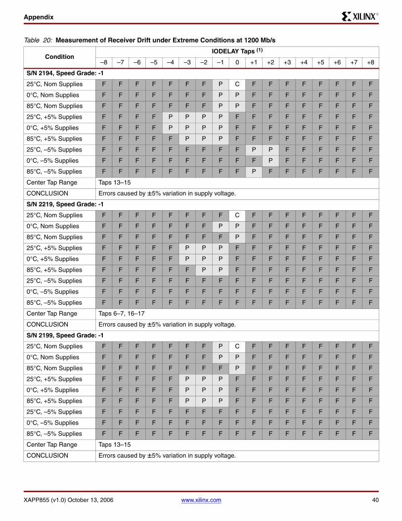
Appendix
XAPP855 (v10) October 13 2006 wwwxilinxcom 40
R
Table 20 Measurement of Receiver Drift under Extreme Conditions at 1200 Mbs
ConditionIODELAY Taps (1)
ndash8 ndash7 ndash6 ndash5 ndash4 ndash3 ndash2 ndash1 0 +1 +2 +3 +4 +5 +6 +7 +8
SN 2194 Speed Grade -1
25degC Nom Supplies F F F F F F F P C F F F F F F F F
0degC Nom Supplies F F F F F F F P P F F F F F F F F
85degC Nom Supplies F F F F F F F P P F F F F F F F F
25degC +5 Supplies F F F F P P P P F F F F F F F F F
0degC +5 Supplies F F F F P P P P F F F F F F F F F
85degC +5 Supplies F F F F F P P P F F F F F F F F F
25degC ndash5 Supplies F F F F F F F F F P P F F F F F F
0degC ndash5 Supplies F F F F F F F F F F P F F F F F F
85degC ndash5 Supplies F F F F F F F F F P F F F F F F F
Center Tap Range Taps 13ndash15
CONCLUSION Errors caused by plusmn5 variation in supply voltage
SN 2219 Speed Grade -1
25degC Nom Supplies F F F F F F F F C F F F F F F F F
0degC Nom Supplies F F F F F F F P P F F F F F F F F
85degC Nom Supplies F F F F F F F F P F F F F F F F F
25degC +5 Supplies F F F F F P P P F F F F F F F F F
0degC +5 Supplies F F F F F P P P F F F F F F F F F
85degC +5 Supplies F F F F F F P P F F F F F F F F F
25degC ndash5 Supplies F F F F F F F F F F F F F F F F F
0degC ndash5 Supplies F F F F F F F F F F F F F F F F F
85degC ndash5 Supplies F F F F F F F F F F F F F F F F F
Center Tap Range Taps 6ndash7 16ndash17
CONCLUSION Errors caused by plusmn5 variation in supply voltage
SN 2199 Speed Grade -1
25degC Nom Supplies F F F F F F F P C F F F F F F F F
0degC Nom Supplies F F F F F F F P P F F F F F F F F
85degC Nom Supplies F F F F F F F F P F F F F F F F F
25degC +5 Supplies F F F F F P P P F F F F F F F F F
0degC +5 Supplies F F F F F P P P F F F F F F F F F
85degC +5 Supplies F F F F F P P P F F F F F F F F F
25degC ndash5 Supplies F F F F F F F F F F F F F F F F F
0degC ndash5 Supplies F F F F F F F F F F F F F F F F F
85degC ndash5 Supplies F F F F F F F F F F F F F F F F F
Center Tap Range Taps 13ndash15
CONCLUSION Errors caused by plusmn5 variation in supply voltage
Appendix
XAPP855 (v10) October 13 2006 wwwxilinxcom 41
R
SN 001 Speed Grade -2
25degC Nom Supplies F F F F F F F P C P F F F F F F F
0degC Nom Supplies F F F F F F F P P P F F F F F F F
85degC Nom Supplies F F F F F F F P P P F F F F F F F
25degC +5 Supplies F F F F F P P P P F F F F F F F F
0degC +5 Supplies F F F F P P P P P F F F F F F F F
85degC +5 Supplies F F F F F P P P P F F F F F F F F
25degC ndash5 Supplies F F F F F F F F F F P F F F F F F
0degC ndash5 Supplies F F F F F F F F F F P F F F F F F
85degC ndash5 Supplies F F F F F F F F F F P F F F F F F
Center Tap Range Taps 12ndash13
CONCLUSION Errors caused by ndash5 variation in supply voltage
SN 002 Speed Grade -2
25degC Nom Supplies F F F F F F P P C P F F F F F F F
0degC Nom Supplies F F F F F F P P P P F F F F F F F
85degC Nom Supplies F F F F F F F P P P F F F F F F F
25degC +5 Supplies F F F F P P P P F F F F F F F F F
0degC +5 Supplies F F F F P P P P F F F F F F F F F
85degC +5 Supplies F F F F F P P P F F F F F F F F F
25degC ndash5 Supplies F F F F F F F F P P P F F F F F F
0degC ndash5 Supplies F F F F F F F F P P P F F F F F F
85degC ndash5 Supplies F F F F F F F F F P P F F F F F F
Center Tap Range Taps 13ndash14
CONCLUSION Errors caused by plusmn5 variation in supply voltage
SN 003 Speed Grade -2
25degC Nom Supplies F F F F F F F P C F F F F F F F F
0degC Nom Supplies F F F F F F F P P F F F F F F F F
85degC Nom Supplies F F F F F F F F P F F F F F F F F
25degC +5 Supplies F F F F F P P P F F F F F F F F F
0degC +5 Supplies F F F F F P P P F F F F F F F F F
85degC +5 Supplies F F F F F F P P F F F F F F F F F
25degC ndash5 Supplies F F F F F F F F F F F F F F F F F
0degC ndash5 Supplies F F F F F F F F F F F F F F F F F
85degC ndash5 Supplies F F F F F F F F F F F F F F F F F
Center Tap Range Taps 14ndash15
CONCLUSION Errors caused by plusmn5 variation in supply voltage
Table 20 Measurement of Receiver Drift under Extreme Conditions at 1200 Mbs (Continued)
ConditionIODELAY Taps (1)
ndash8 ndash7 ndash6 ndash5 ndash4 ndash3 ndash2 ndash1 0 +1 +2 +3 +4 +5 +6 +7 +8
Appendix
XAPP855 (v10) October 13 2006 wwwxilinxcom 42
R
SN 004 Speed Grade -3
25degC Nom Supplies F F F F F F P P C P F F F F F F F
0degC Nom Supplies F F F F F P P P P P F F F F F F F
85degC Nom Supplies F F F F F F P P P P F F F F F F F
25degC +5 Supplies F F F F P P P P P F F F F F F F F
0degC +5 Supplies F F F F P P P P P F F F F F F F F
85degC +5 Supplies F F F F F P P P P F F F F F F F F
25degC ndash5 Supplies F F F F F F F F P P P F F F F F F
0degC ndash5 Supplies F F F F F F F F P P P F F F F F F
85degC ndash5 Supplies F F F F F F F F P P P F F F F F F
Center Tap Range Taps 9ndash11
CONCLUSION Error free under all conditions when calibrated under nominal conditions to position C
SN 005 Speed Grade -3
25degC Nom Supplies F F F F F P P P C P F F F F F F F
0degC Nom Supplies F F F F F P P P P P F F F F F F F
85degC Nom Supplies F F F F F F P P P P F F F F F F F
25degC +5 Supplies F F F F P P P P P F F F F F F F F
0degC +5 Supplies F F F P P P P P P F F F F F F F F
85degC +5 Supplies F F F F P P P P P F F F F F F F F
25degC ndash5 Supplies F F F F F F F P P P P P F F F F F
0degC ndash5 Supplies F F F F F F F P P P P P F F F F F
85degC ndash5 Supplies F F F F F F F F P P P F F F F F F
Center Tap Range Taps 11ndash13
CONCLUSION Error free under all conditions when calibrated under nominal conditions to position C
SN 006 Speed Grade -3
25degC Nom Supplies F F F F F P P P C P F F F F F F F
0degC Nom Supplies F F F F F P P P P P F F F F F F F
85degC Nom Supplies F F F F F P P P P P F F F F F F F
25degC +5 Supplies F F F P P P P P P F F F F F F F F
0degC +5 Supplies F F F P P P P P P F F F F F F F F
85degC +5 Supplies F F F F P P P P P F F F F F F F F
25degC ndash5 Supplies F F F F F F F P P P P F F F F F F
0degC ndash5 Supplies F F F F F F P P P P P F F F F F F
85degC ndash5 Supplies F F F F F F F P P P P F F F F F F
Center Tap Range Taps 10ndash11
CONCLUSION Error free under all conditions when calibrated under nominal conditions to position C
Notes 1 IODELAY taps where 0 is the reference tap determined by the bit align machine at nominal voltage and 25degC2 P = Error-free transmission F = Error in transmission C = IODELAY tap position selected by bit-align machine under nominal conditions at 25degC
Table 20 Measurement of Receiver Drift under Extreme Conditions at 1200 Mbs (Continued)
ConditionIODELAY Taps (1)
ndash8 ndash7 ndash6 ndash5 ndash4 ndash3 ndash2 ndash1 0 +1 +2 +3 +4 +5 +6 +7 +8
Revision History
XAPP855 (v10) October 13 2006 wwwxilinxcom 43
R
Revision History
The following table shows the revision history for this document
Date Version Revision
101306 10 Initial Xilinx release
- 16-Channel DDR LVDS Interface with Per-Channel Alignment
-
- Summary
- Introduction
-
- Figure 1 Full-Duplex 16-Channel DDR Link between a Virtex-5 Device and Another Device with a 16-Channel DDR Interface
- Figure 2 BERT Testbench for Hardware Verification of the DDR Interface
- Figure 3 Design Hierarchy of the Interface (TX and RX)
-
- DDR Transmitter
-
- Table 1 DDR_8TO1_16CHAN_TX Module Port Definitions
- Figure 4 MasterSlave OSERDES Pair for a Single Data Channel with 81 Serialization
- Figure 5 Block Diagram of TX Interface
- Table 2 DDR TX Interface Utilization Statistics
-
- Interface Clocking
-
- Figure 6 Global and Regional Clocking Schemes in Virtex-5 FPGAs
- Table 3 Comparison of Global and IO Clock Performance by Speed Grade
-
- DDR Receiver
-
- Table 4 DDR_8TO1_16CHAN_RX Module Port Definitions
- Figure 7 MasterSlave ISERDES Pair for a Single Data Channel with 18 Deserialization
- Figure 8 Block Diagram of RX Interface
- Table 5 DDR RX Interface Utilization Statistics
-
- Receiver Interface Dynamic Timing
-
- Inherent Timing
-
- Figure 9 Timing Components of RX Data and Clock Paths
- Figure 10 ISE Timing Analyzer Properties Used in this Document
- Table 6 Datapath Timing Definitions
- Table 7 Clock Path Timing Definitions
- Table 8 Datapath Delay Inventory for a -1 Speed Grade XC5VLX50T Device
- Table 9 Clock Path Delay Inventory for a -1 Speed Grade XC5VLX50T Device
- Figure 11 Timing Windows Show Uncertainty in ClockData Relationship as Calculated by Timing Analyzer
-
- Dynamic Timing and BIT_ALIGN_MACHINE
-
- Figure 12 Inherent Timing Windows Shown in Relation to Multiple Data Rates
- Figure 13 Dynamic Bit-Alignment Procedure in BIT_ALIGN_MACHINE
- Table 10 Word Alignment in the DDR Receiver
- Figure 14 FSM in the BIT_ALIGN_MACHINE Module
-
- Interface Timing Budget
-
- Interface Characterization
-
- Figure 15 Bit-Alignment Algorithm Performance
- Table 11 Tap Setting Range For Various Data Rates Measured on a -2 Device
- Table 12 Measurement of Receiver Drift under Extreme Conditions for Multiple Data Rates
- Pattern Dependence of Receiver Performance
-
- Table 13 Link Performance for Various Types of Data Measured on a -2 Device
-
- Resetting the Interface
-
- Figure 16 Recommended Interface Reset Timing
-
- Conclusion
-
- Table 14 Performance of 16-Channel DDR Interface
-
- Appendix
-
- Performance Characterization Data
-
- Table 15 Summary of Interface Characterization Results
- Table 16 Measurement of Receiver Drift under Extreme Conditions at 800 Mbs
- Table 17 Measurement of Receiver Drift under Extreme Conditions at 900 Mbs
- Table 18 Measurement of Receiver Drift under Extreme Conditions at 1000 Mbs
- Table 19 Measurement of Receiver Drift under Extreme Conditions at 1100 Mbs
- Table 20 Measurement of Receiver Drift under Extreme Conditions at 1200 Mbs
-
- Revision History
-
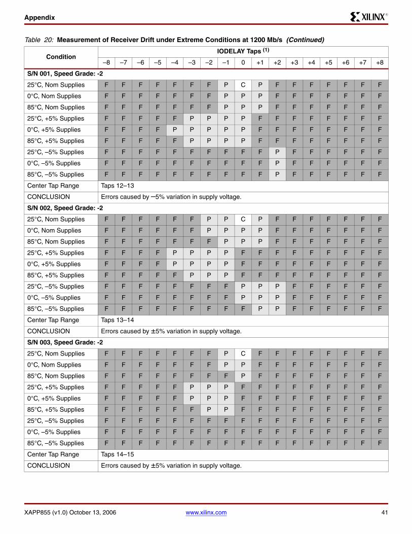
Appendix
XAPP855 (v10) October 13 2006 wwwxilinxcom 41
R
SN 001 Speed Grade -2
25degC Nom Supplies F F F F F F F P C P F F F F F F F
0degC Nom Supplies F F F F F F F P P P F F F F F F F
85degC Nom Supplies F F F F F F F P P P F F F F F F F
25degC +5 Supplies F F F F F P P P P F F F F F F F F
0degC +5 Supplies F F F F P P P P P F F F F F F F F
85degC +5 Supplies F F F F F P P P P F F F F F F F F
25degC ndash5 Supplies F F F F F F F F F F P F F F F F F
0degC ndash5 Supplies F F F F F F F F F F P F F F F F F
85degC ndash5 Supplies F F F F F F F F F F P F F F F F F
Center Tap Range Taps 12ndash13
CONCLUSION Errors caused by ndash5 variation in supply voltage
SN 002 Speed Grade -2
25degC Nom Supplies F F F F F F P P C P F F F F F F F
0degC Nom Supplies F F F F F F P P P P F F F F F F F
85degC Nom Supplies F F F F F F F P P P F F F F F F F
25degC +5 Supplies F F F F P P P P F F F F F F F F F
0degC +5 Supplies F F F F P P P P F F F F F F F F F
85degC +5 Supplies F F F F F P P P F F F F F F F F F
25degC ndash5 Supplies F F F F F F F F P P P F F F F F F
0degC ndash5 Supplies F F F F F F F F P P P F F F F F F
85degC ndash5 Supplies F F F F F F F F F P P F F F F F F
Center Tap Range Taps 13ndash14
CONCLUSION Errors caused by plusmn5 variation in supply voltage
SN 003 Speed Grade -2
25degC Nom Supplies F F F F F F F P C F F F F F F F F
0degC Nom Supplies F F F F F F F P P F F F F F F F F
85degC Nom Supplies F F F F F F F F P F F F F F F F F
25degC +5 Supplies F F F F F P P P F F F F F F F F F
0degC +5 Supplies F F F F F P P P F F F F F F F F F
85degC +5 Supplies F F F F F F P P F F F F F F F F F
25degC ndash5 Supplies F F F F F F F F F F F F F F F F F
0degC ndash5 Supplies F F F F F F F F F F F F F F F F F
85degC ndash5 Supplies F F F F F F F F F F F F F F F F F
Center Tap Range Taps 14ndash15
CONCLUSION Errors caused by plusmn5 variation in supply voltage
Table 20 Measurement of Receiver Drift under Extreme Conditions at 1200 Mbs (Continued)
ConditionIODELAY Taps (1)
ndash8 ndash7 ndash6 ndash5 ndash4 ndash3 ndash2 ndash1 0 +1 +2 +3 +4 +5 +6 +7 +8
Appendix
XAPP855 (v10) October 13 2006 wwwxilinxcom 42
R
SN 004 Speed Grade -3
25degC Nom Supplies F F F F F F P P C P F F F F F F F
0degC Nom Supplies F F F F F P P P P P F F F F F F F
85degC Nom Supplies F F F F F F P P P P F F F F F F F
25degC +5 Supplies F F F F P P P P P F F F F F F F F
0degC +5 Supplies F F F F P P P P P F F F F F F F F
85degC +5 Supplies F F F F F P P P P F F F F F F F F
25degC ndash5 Supplies F F F F F F F F P P P F F F F F F
0degC ndash5 Supplies F F F F F F F F P P P F F F F F F
85degC ndash5 Supplies F F F F F F F F P P P F F F F F F
Center Tap Range Taps 9ndash11
CONCLUSION Error free under all conditions when calibrated under nominal conditions to position C
SN 005 Speed Grade -3
25degC Nom Supplies F F F F F P P P C P F F F F F F F
0degC Nom Supplies F F F F F P P P P P F F F F F F F
85degC Nom Supplies F F F F F F P P P P F F F F F F F
25degC +5 Supplies F F F F P P P P P F F F F F F F F
0degC +5 Supplies F F F P P P P P P F F F F F F F F
85degC +5 Supplies F F F F P P P P P F F F F F F F F
25degC ndash5 Supplies F F F F F F F P P P P P F F F F F
0degC ndash5 Supplies F F F F F F F P P P P P F F F F F
85degC ndash5 Supplies F F F F F F F F P P P F F F F F F
Center Tap Range Taps 11ndash13
CONCLUSION Error free under all conditions when calibrated under nominal conditions to position C
SN 006 Speed Grade -3
25degC Nom Supplies F F F F F P P P C P F F F F F F F
0degC Nom Supplies F F F F F P P P P P F F F F F F F
85degC Nom Supplies F F F F F P P P P P F F F F F F F
25degC +5 Supplies F F F P P P P P P F F F F F F F F
0degC +5 Supplies F F F P P P P P P F F F F F F F F
85degC +5 Supplies F F F F P P P P P F F F F F F F F
25degC ndash5 Supplies F F F F F F F P P P P F F F F F F
0degC ndash5 Supplies F F F F F F P P P P P F F F F F F
85degC ndash5 Supplies F F F F F F F P P P P F F F F F F
Center Tap Range Taps 10ndash11
CONCLUSION Error free under all conditions when calibrated under nominal conditions to position C
Notes 1 IODELAY taps where 0 is the reference tap determined by the bit align machine at nominal voltage and 25degC2 P = Error-free transmission F = Error in transmission C = IODELAY tap position selected by bit-align machine under nominal conditions at 25degC
Table 20 Measurement of Receiver Drift under Extreme Conditions at 1200 Mbs (Continued)
ConditionIODELAY Taps (1)
ndash8 ndash7 ndash6 ndash5 ndash4 ndash3 ndash2 ndash1 0 +1 +2 +3 +4 +5 +6 +7 +8
Revision History
XAPP855 (v10) October 13 2006 wwwxilinxcom 43
R
Revision History
The following table shows the revision history for this document
Date Version Revision
101306 10 Initial Xilinx release
- 16-Channel DDR LVDS Interface with Per-Channel Alignment
-
- Summary
- Introduction
-
- Figure 1 Full-Duplex 16-Channel DDR Link between a Virtex-5 Device and Another Device with a 16-Channel DDR Interface
- Figure 2 BERT Testbench for Hardware Verification of the DDR Interface
- Figure 3 Design Hierarchy of the Interface (TX and RX)
-
- DDR Transmitter
-
- Table 1 DDR_8TO1_16CHAN_TX Module Port Definitions
- Figure 4 MasterSlave OSERDES Pair for a Single Data Channel with 81 Serialization
- Figure 5 Block Diagram of TX Interface
- Table 2 DDR TX Interface Utilization Statistics
-
- Interface Clocking
-
- Figure 6 Global and Regional Clocking Schemes in Virtex-5 FPGAs
- Table 3 Comparison of Global and IO Clock Performance by Speed Grade
-
- DDR Receiver
-
- Table 4 DDR_8TO1_16CHAN_RX Module Port Definitions
- Figure 7 MasterSlave ISERDES Pair for a Single Data Channel with 18 Deserialization
- Figure 8 Block Diagram of RX Interface
- Table 5 DDR RX Interface Utilization Statistics
-
- Receiver Interface Dynamic Timing
-
- Inherent Timing
-
- Figure 9 Timing Components of RX Data and Clock Paths
- Figure 10 ISE Timing Analyzer Properties Used in this Document
- Table 6 Datapath Timing Definitions
- Table 7 Clock Path Timing Definitions
- Table 8 Datapath Delay Inventory for a -1 Speed Grade XC5VLX50T Device
- Table 9 Clock Path Delay Inventory for a -1 Speed Grade XC5VLX50T Device
- Figure 11 Timing Windows Show Uncertainty in ClockData Relationship as Calculated by Timing Analyzer
-
- Dynamic Timing and BIT_ALIGN_MACHINE
-
- Figure 12 Inherent Timing Windows Shown in Relation to Multiple Data Rates
- Figure 13 Dynamic Bit-Alignment Procedure in BIT_ALIGN_MACHINE
- Table 10 Word Alignment in the DDR Receiver
- Figure 14 FSM in the BIT_ALIGN_MACHINE Module
-
- Interface Timing Budget
-
- Interface Characterization
-
- Figure 15 Bit-Alignment Algorithm Performance
- Table 11 Tap Setting Range For Various Data Rates Measured on a -2 Device
- Table 12 Measurement of Receiver Drift under Extreme Conditions for Multiple Data Rates
- Pattern Dependence of Receiver Performance
-
- Table 13 Link Performance for Various Types of Data Measured on a -2 Device
-
- Resetting the Interface
-
- Figure 16 Recommended Interface Reset Timing
-
- Conclusion
-
- Table 14 Performance of 16-Channel DDR Interface
-
- Appendix
-
- Performance Characterization Data
-
- Table 15 Summary of Interface Characterization Results
- Table 16 Measurement of Receiver Drift under Extreme Conditions at 800 Mbs
- Table 17 Measurement of Receiver Drift under Extreme Conditions at 900 Mbs
- Table 18 Measurement of Receiver Drift under Extreme Conditions at 1000 Mbs
- Table 19 Measurement of Receiver Drift under Extreme Conditions at 1100 Mbs
- Table 20 Measurement of Receiver Drift under Extreme Conditions at 1200 Mbs
-
- Revision History
-
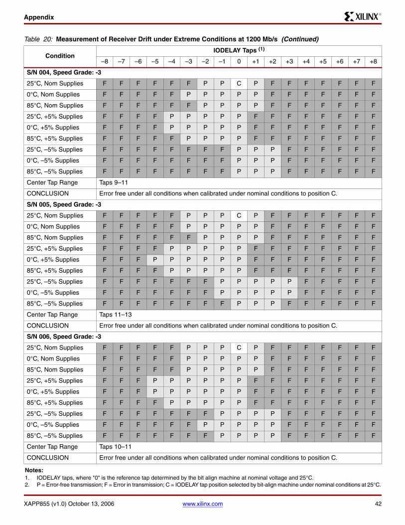
Appendix
XAPP855 (v10) October 13 2006 wwwxilinxcom 42
R
SN 004 Speed Grade -3
25degC Nom Supplies F F F F F F P P C P F F F F F F F
0degC Nom Supplies F F F F F P P P P P F F F F F F F
85degC Nom Supplies F F F F F F P P P P F F F F F F F
25degC +5 Supplies F F F F P P P P P F F F F F F F F
0degC +5 Supplies F F F F P P P P P F F F F F F F F
85degC +5 Supplies F F F F F P P P P F F F F F F F F
25degC ndash5 Supplies F F F F F F F F P P P F F F F F F
0degC ndash5 Supplies F F F F F F F F P P P F F F F F F
85degC ndash5 Supplies F F F F F F F F P P P F F F F F F
Center Tap Range Taps 9ndash11
CONCLUSION Error free under all conditions when calibrated under nominal conditions to position C
SN 005 Speed Grade -3
25degC Nom Supplies F F F F F P P P C P F F F F F F F
0degC Nom Supplies F F F F F P P P P P F F F F F F F
85degC Nom Supplies F F F F F F P P P P F F F F F F F
25degC +5 Supplies F F F F P P P P P F F F F F F F F
0degC +5 Supplies F F F P P P P P P F F F F F F F F
85degC +5 Supplies F F F F P P P P P F F F F F F F F
25degC ndash5 Supplies F F F F F F F P P P P P F F F F F
0degC ndash5 Supplies F F F F F F F P P P P P F F F F F
85degC ndash5 Supplies F F F F F F F F P P P F F F F F F
Center Tap Range Taps 11ndash13
CONCLUSION Error free under all conditions when calibrated under nominal conditions to position C
SN 006 Speed Grade -3
25degC Nom Supplies F F F F F P P P C P F F F F F F F
0degC Nom Supplies F F F F F P P P P P F F F F F F F
85degC Nom Supplies F F F F F P P P P P F F F F F F F
25degC +5 Supplies F F F P P P P P P F F F F F F F F
0degC +5 Supplies F F F P P P P P P F F F F F F F F
85degC +5 Supplies F F F F P P P P P F F F F F F F F
25degC ndash5 Supplies F F F F F F F P P P P F F F F F F
0degC ndash5 Supplies F F F F F F P P P P P F F F F F F
85degC ndash5 Supplies F F F F F F F P P P P F F F F F F
Center Tap Range Taps 10ndash11
CONCLUSION Error free under all conditions when calibrated under nominal conditions to position C
Notes 1 IODELAY taps where 0 is the reference tap determined by the bit align machine at nominal voltage and 25degC2 P = Error-free transmission F = Error in transmission C = IODELAY tap position selected by bit-align machine under nominal conditions at 25degC
Table 20 Measurement of Receiver Drift under Extreme Conditions at 1200 Mbs (Continued)
ConditionIODELAY Taps (1)
ndash8 ndash7 ndash6 ndash5 ndash4 ndash3 ndash2 ndash1 0 +1 +2 +3 +4 +5 +6 +7 +8
Revision History
XAPP855 (v10) October 13 2006 wwwxilinxcom 43
R
Revision History
The following table shows the revision history for this document
Date Version Revision
101306 10 Initial Xilinx release
- 16-Channel DDR LVDS Interface with Per-Channel Alignment
-
- Summary
- Introduction
-
- Figure 1 Full-Duplex 16-Channel DDR Link between a Virtex-5 Device and Another Device with a 16-Channel DDR Interface
- Figure 2 BERT Testbench for Hardware Verification of the DDR Interface
- Figure 3 Design Hierarchy of the Interface (TX and RX)
-
- DDR Transmitter
-
- Table 1 DDR_8TO1_16CHAN_TX Module Port Definitions
- Figure 4 MasterSlave OSERDES Pair for a Single Data Channel with 81 Serialization
- Figure 5 Block Diagram of TX Interface
- Table 2 DDR TX Interface Utilization Statistics
-
- Interface Clocking
-
- Figure 6 Global and Regional Clocking Schemes in Virtex-5 FPGAs
- Table 3 Comparison of Global and IO Clock Performance by Speed Grade
-
- DDR Receiver
-
- Table 4 DDR_8TO1_16CHAN_RX Module Port Definitions
- Figure 7 MasterSlave ISERDES Pair for a Single Data Channel with 18 Deserialization
- Figure 8 Block Diagram of RX Interface
- Table 5 DDR RX Interface Utilization Statistics
-
- Receiver Interface Dynamic Timing
-
- Inherent Timing
-
- Figure 9 Timing Components of RX Data and Clock Paths
- Figure 10 ISE Timing Analyzer Properties Used in this Document
- Table 6 Datapath Timing Definitions
- Table 7 Clock Path Timing Definitions
- Table 8 Datapath Delay Inventory for a -1 Speed Grade XC5VLX50T Device
- Table 9 Clock Path Delay Inventory for a -1 Speed Grade XC5VLX50T Device
- Figure 11 Timing Windows Show Uncertainty in ClockData Relationship as Calculated by Timing Analyzer
-
- Dynamic Timing and BIT_ALIGN_MACHINE
-
- Figure 12 Inherent Timing Windows Shown in Relation to Multiple Data Rates
- Figure 13 Dynamic Bit-Alignment Procedure in BIT_ALIGN_MACHINE
- Table 10 Word Alignment in the DDR Receiver
- Figure 14 FSM in the BIT_ALIGN_MACHINE Module
-
- Interface Timing Budget
-
- Interface Characterization
-
- Figure 15 Bit-Alignment Algorithm Performance
- Table 11 Tap Setting Range For Various Data Rates Measured on a -2 Device
- Table 12 Measurement of Receiver Drift under Extreme Conditions for Multiple Data Rates
- Pattern Dependence of Receiver Performance
-
- Table 13 Link Performance for Various Types of Data Measured on a -2 Device
-
- Resetting the Interface
-
- Figure 16 Recommended Interface Reset Timing
-
- Conclusion
-
- Table 14 Performance of 16-Channel DDR Interface
-
- Appendix
-
- Performance Characterization Data
-
- Table 15 Summary of Interface Characterization Results
- Table 16 Measurement of Receiver Drift under Extreme Conditions at 800 Mbs
- Table 17 Measurement of Receiver Drift under Extreme Conditions at 900 Mbs
- Table 18 Measurement of Receiver Drift under Extreme Conditions at 1000 Mbs
- Table 19 Measurement of Receiver Drift under Extreme Conditions at 1100 Mbs
- Table 20 Measurement of Receiver Drift under Extreme Conditions at 1200 Mbs
-
- Revision History
-
Revision History
XAPP855 (v10) October 13 2006 wwwxilinxcom 43
R
Revision History
The following table shows the revision history for this document
Date Version Revision
101306 10 Initial Xilinx release
- 16-Channel DDR LVDS Interface with Per-Channel Alignment
-
- Summary
- Introduction
-
- Figure 1 Full-Duplex 16-Channel DDR Link between a Virtex-5 Device and Another Device with a 16-Channel DDR Interface
- Figure 2 BERT Testbench for Hardware Verification of the DDR Interface
- Figure 3 Design Hierarchy of the Interface (TX and RX)
-
- DDR Transmitter
-
- Table 1 DDR_8TO1_16CHAN_TX Module Port Definitions
- Figure 4 MasterSlave OSERDES Pair for a Single Data Channel with 81 Serialization
- Figure 5 Block Diagram of TX Interface
- Table 2 DDR TX Interface Utilization Statistics
-
- Interface Clocking
-
- Figure 6 Global and Regional Clocking Schemes in Virtex-5 FPGAs
- Table 3 Comparison of Global and IO Clock Performance by Speed Grade
-
- DDR Receiver
-
- Table 4 DDR_8TO1_16CHAN_RX Module Port Definitions
- Figure 7 MasterSlave ISERDES Pair for a Single Data Channel with 18 Deserialization
- Figure 8 Block Diagram of RX Interface
- Table 5 DDR RX Interface Utilization Statistics
-
- Receiver Interface Dynamic Timing
-
- Inherent Timing
-
- Figure 9 Timing Components of RX Data and Clock Paths
- Figure 10 ISE Timing Analyzer Properties Used in this Document
- Table 6 Datapath Timing Definitions
- Table 7 Clock Path Timing Definitions
- Table 8 Datapath Delay Inventory for a -1 Speed Grade XC5VLX50T Device
- Table 9 Clock Path Delay Inventory for a -1 Speed Grade XC5VLX50T Device
- Figure 11 Timing Windows Show Uncertainty in ClockData Relationship as Calculated by Timing Analyzer
-
- Dynamic Timing and BIT_ALIGN_MACHINE
-
- Figure 12 Inherent Timing Windows Shown in Relation to Multiple Data Rates
- Figure 13 Dynamic Bit-Alignment Procedure in BIT_ALIGN_MACHINE
- Table 10 Word Alignment in the DDR Receiver
- Figure 14 FSM in the BIT_ALIGN_MACHINE Module
-
- Interface Timing Budget
-
- Interface Characterization
-
- Figure 15 Bit-Alignment Algorithm Performance
- Table 11 Tap Setting Range For Various Data Rates Measured on a -2 Device
- Table 12 Measurement of Receiver Drift under Extreme Conditions for Multiple Data Rates
- Pattern Dependence of Receiver Performance
-
- Table 13 Link Performance for Various Types of Data Measured on a -2 Device
-
- Resetting the Interface
-
- Figure 16 Recommended Interface Reset Timing
-
- Conclusion
-
- Table 14 Performance of 16-Channel DDR Interface
-
- Appendix
-
- Performance Characterization Data
-
- Table 15 Summary of Interface Characterization Results
- Table 16 Measurement of Receiver Drift under Extreme Conditions at 800 Mbs
- Table 17 Measurement of Receiver Drift under Extreme Conditions at 900 Mbs
- Table 18 Measurement of Receiver Drift under Extreme Conditions at 1000 Mbs
- Table 19 Measurement of Receiver Drift under Extreme Conditions at 1100 Mbs
- Table 20 Measurement of Receiver Drift under Extreme Conditions at 1200 Mbs
-
- Revision History
-