Application Note AN101 · Preprocessor Defined symbols in IAR ... then control jumps to the...
29
Application Note AN101 SWRA371A-Sep 2011 Page 1 of 28 Bootloader for CC2510, CC2511, CC1110 and CC1111 SoC (System-on-Chip) Transceivers By Shashank Mane Keywords Bootloader Firmware Update Flash read/write SPI interface DMA controller Boot loader testing 1 Introduction This document describes the details of a boot loader which can be used for the CC2510, CC2511, CC1110 or CC1111 SoC transceivers. It covers the overall flow of the boot loader, a line by line description of the code, the test environment to test/drive the boot loader and sample LED blinking code to verify the functionality of the boot loader. Whenever the chip gets reset, control jumps to the starting point of the boot loader where, based on the validity of the firmware (i.e., application code), the boot loader will either accept commands from the user and program the new firmware into the flash or will directly jump to the starting point of the already existing valid firmware in the flash. So the task of the boot loader is to validate the firmware present in the flash and then decide to either program the user specified firmware or jump to the existing firmware. This boot loader code is derived from the boot loader for the CC2530 [1]. Based on the transceiver used, define CC2510, CC2511, CC1110 or CC1111 in the options C/C++ Compiler Preprocessor Defined symbols in IAR embedded work bench.
Transcript of Application Note AN101 · Preprocessor Defined symbols in IAR ... then control jumps to the...
Application Note AN101
SWRA371A-Sep 2011 Page 1 of 28
Bootloader for CC2510, CC2511, CC1110 and CC1111 SoC (System-on-Chip) Transceivers
By Shashank Mane Keywords
Bootloader Firmware Update Flash read/write SPI interface
DMA controller Boot loader testing
1 Introduction
This document describes the details of a boot loader which can be used for the CC2510, CC2511, CC1110 or CC1111 SoC transceivers. It covers the overall flow of the boot loader, a line by line description of the code, the test environment to test/drive the boot loader and sample LED blinking code to verify the functionality of the boot loader. Whenever the chip gets reset, control jumps to the starting point of the boot loader where, based on the validity of the firmware (i.e., application code), the boot loader will either accept commands from the user and program the new firmware into the flash or will directly jump to the starting point of the already existing valid
firmware in the flash. So the task of the boot loader is to validate the firmware present in the flash and then decide to either program the user specified firmware or jump to the existing firmware. This boot loader code is derived from the boot loader for the CC2530 [1]. Based on the transceiver used, define CC2510, CC2511, CC1110 or CC1111 in the options C/C++ Compiler Preprocessor Defined symbols in IAR embedded work bench.

Application Note AN101
SWRA371A-Sep 2011 Page 2 of 28
Table of Contents 1 Introduction ..............................................................................................................................1 2 Introduction to the boot loader...................................................................................................3
2.1 Overall flow of the boot loader..............................................................................................4 3 Code description .......................................................................................................................7
3.1 sblInit(): ...............................................................................................................................8 3.2 sbImgValid(): .......................................................................................................................8 3.3 sblWait(): .............................................................................................................................9 3.4 HalUARTUnInitISR():........................................................................................................10 3.5 sblExec(): ........................................................................................................................... 10 3.6 sbExec(): ............................................................................................................................ 10 3.7 sbCmnd(): .......................................................................................................................... 11 3.8 ISR in the boot loader .........................................................................................................14 3.9 DMA controller for flash write ........................................................................................... 15
4 Frame Format ......................................................................................................................... 16 4.1 Command from external host.............................................................................................. 17 4.2 Response to the command...................................................................................................19
5 Test Environment.................................................................................................................... 22 6 Sample LED blinking code......................................................................................................23 7 FAQ........................................................................................................................................26 8 References............................................................................................................................... 28
8.1 Cited references .................................................................................................................. 28 8.2 General references .............................................................................................................. 28
9 Document History ................................................................................................................... 28

Application Note AN101
SWRA371A-Sep 2011 Page 3 of 28
2 Introduction to the boot loader
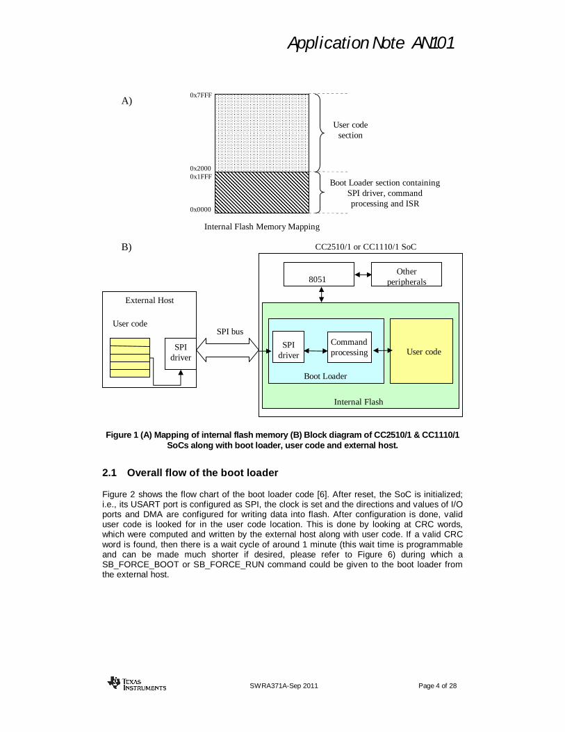
This section gives an introduction to the boot loader for the CC2510/1 & CC1110/1 SoC transceivers (in this document, we will refer to CC2510/1 and CC1110/1 transceivers as SoCs). A boot loader is mainly used to load the program (user code) into the code memory area of the microcontroller. It is the first thing that is performed after the microcontroller is powered up. In the case of the SoCs, the user code needs to be written into the internal flash memory of the SoCs. In order to load the user code into the internal flash, there should be a small program present inside the internal flash that performs the task of interacting with the external world and writing the user code into the specified location of internal flash. This set of code is called the boot loader. After reset, the program counter of the microcontroller is always set to the starting point of the boot loader. The boot loader will first look for valid user code (by looking at the CRC words stored in a specific location of internal flash) in the internal flash. If it finds valid user code, then control jumps to the starting point of the user code. Before entering the user code, there is a fixed wait time of a small duration, during which the microcontroller can be forced to enter the boot loader execution sequence. In the boot loader execution sequence, the user may write new user code into the internal flash. [1][2][5] Figure 1 shows the block diagram of the SoC showing its flash memory, boot loader code location, user code location and external host that interacts with the boot loader to write the user code.
Application Note AN101
SWRA371A-Sep 2011 Page 4 of 28
Figure 1 (A) Mapping of internal flash memory (B) Block diagram of CC2510/1 & CC1110/1
SoCs along with boot loader, user code and external host.
2.1 Overall flow of the boot loader
Figure 2 shows the flow chart of the boot loader code [6]. After reset, the SoC is initialized; i.e., its USART port is configured as SPI, the clock is set and the directions and values of I/O ports and DMA are configured for writing data into flash. After configuration is done, valid user code is looked for in the user code location. This is done by looking at CRC words, which were computed and written by the external host along with user code. If a valid CRC word is found, then there is a wait cycle of around 1 minute (this wait time is programmable and can be made much shorter if desired, please refer to Figure 6) during which a SB_FORCE_BOOT or SB_FORCE_RUN command could be given to the boot loader from the external host.
CC2510/1 or CC1110/1 SoC
External Host
SPI driver
User code SPI bus
SPI driver
Boot Loader
User code
Internal Flash
8051 Other
peripherals
Command processing
B)
0x2000
0x0000
Internal Flash Memory Mapping
0x7FFF
Boot Loader section containing SPI driver, command processing and ISR
User code section
0x1FFF
A)

Application Note AN101
SWRA371A-Sep 2011 Page 5 of 28
Figure 2 Flow chart of the boot loader [6].
If a SB_FORCE_RUN command is given, then control jumps to the predefined start of user code, and if a SB_FORCE_BOOT command is given, then the boot loader routine is executed. A SB_FORCE_RUN command can be generated by the external host by passing 0x07 to the boot loader through the SPI bus, and a SB_FORCE_BOOT command is given by passing 0xF8. If neither of the two commands is given during this wait cycle, control will jump
START
Initialize SoC (CLK, USART, I/O PORT & DMA) - sblInit()
Look for validity of user code - sbImgValid()
Is user code valid (i.e. above function returns
TRUE) ?
Wait for small programmable duration (refer figure 6) (default set to ~ 1 minute) - sblWait()
Yes
No
Is there a request for boot loader execution (i.e. above function returns FALSE)
?
Un-initialize the USART to mimic reset condition - HalUARTUnInitISR()
Yes
No
Jump to the start of user code location i.e. 0x2000
Execute boot loader routine (ie. write user code passed by external host into flash) - sblExec()
Disable interrupts and wait for reset - HAL_SYSTEM_RESET()
END

Application Note AN101
SWRA371A-Sep 2011 Page 6 of 28
to the start of user code by default at the end of this wait cycle. Before jumping to the user code, USART interrupts are reset to avoid false trigger in the user code. During the CRC word validation check, if an invalid CRC word was detected (i.e. no valid user code is present), then control jumps to the execution of boot loader routine. This boot loader routine is used to write valid user code into the user code area of the internal flash of the SoCs. There is a state machine that runs in this routine that looks for a valid frame format (discussed later) generated by the external host and then performs the tasks accordingly. After the complete user code is written into the flash, an enable command is generated by the external host, which will bring the control out of the boot loader routine, and then control can jump to the newly written user code. Figure 2 also shows the function names which are called at various stages of the flow. sblInit() Initializes clock, USART, I/O ports and DMA of the SoC. sbImgValid() Looks for validity of the user code by looking at the CRC word. It returns TRUE when valid user code is found and FALSE when there is no valid user code in the flash and the boot loader routine needs to be run. sblWait() Waits ~1 min during which a SB_FORCE_RUN or SB_FORCE_BOOT command can be issued by external host. This function returns TRUE when user code needs to be run and FALSE when the boot loader routine needs to be executed. sblExec() Executes the boot loader routine that interacts with an external host to write valid user code into the internal flash of the SoC. HalUARTUnInitISR() Resets all the interrupts and configuration registers related to USART to their reset values. HAL_SYSTEM_RESET() Disables interrupts and waits for reset.

Application Note AN101
SWRA371A-Sep 2011 Page 7 of 28
3 Code description
This section gives a detailed description of the boot loader code. Figure 3 shows the function call graph of the boot loader code [6]. Functionality of most of these functions has been described in the previous section. We will go through each function line by line.
Figure 3 Call graph of the boot loader.
Figure 4 shows the snap shot of the main function. First, the sblInit() function is called, which will configure the SoC parameters. Then the sbImgValid() function is called, which will check for valid user code. If it finds valid user code, it will return TRUE and control will enter the first “if” loop.
Figure 4 Snap shot of the main function [1].
main()
sbImgValid()
sblWait()
sblExec()
Clock setting
vddWait()
HalUARTInitISR()
sblInit()
sbExec()
sbCmnd()
Jump to 0x2000
END
Initialize boot loader
Check for validity of user code
Check for voltage level of Vdd
Jump to location 0x2000 where user code is written
Execute boot loader code

Application Note AN101
SWRA371A-Sep 2011 Page 8 of 28
If FALSE is returned, then the “if” condition is not satisfied, so control will skip the loop and will call the sblExec() function, which is the boot loader routine to interact with the external host and write valid user code into the internal flash of SoC. If the sblWait() function is called, then there is a wait time period of around 1 minute during which the boot loader will wait for SB_FORCE_RUN or SB_FORCE_BOOT commands from the external host. If none of these commands is received, then the function returns TRUE at the end of the wait time, and control jumps to the user code after resetting USART interrupt and configuration registers. Now we will describe each function in detail.
3.1 sblInit():
1. Setup Clock – These parameters can be changed if required by referring to the datasheet of the SoCs [3][7]
SLEEP &= ~0x04; //Turning on both the HS oscillator (HS XOSC and HS RCOSC).
while(!(SLEEP & 0x40)); //Wait for HS XOSC to stabilize. CLKCON &= 0xBF; //Selecting HS XOSC. while(CLKCON & 0x40); //Check if HS XOSC was selected as system clock. SLEEP |= 0x04; //Turn off the HS oscillator which was not selected
as system clock (i.e. HS RCOSC is turned off). 2. Turn on cache pre-fetch mode
FCTL = 0x08 3. Set port P1 (to which LEDs are connected) as output ports. By default they are set as
input ports. 4. Call vddWait(VDD_MIN_RUN)
It has a loop which checks for 16 cycles of ADC read value > VDD_MIN_RUN
5. Assign magicByte = SB_MAGIC_VALUE (i.e., 0xF5) Indicates whether bootloader or user code is active. It is used to decide the
location of the interrupt vector table. 6. Configure DMA0 registers DMA0CFGH & DMA0CFGL
Used for writing the data (user code) into the flash 7. Call HalUARTInitISR()
USART is configured in SPI mode. Here it can be changed to UART mode. Other settings associated with it, such as baud rate, flow control, etc is done.
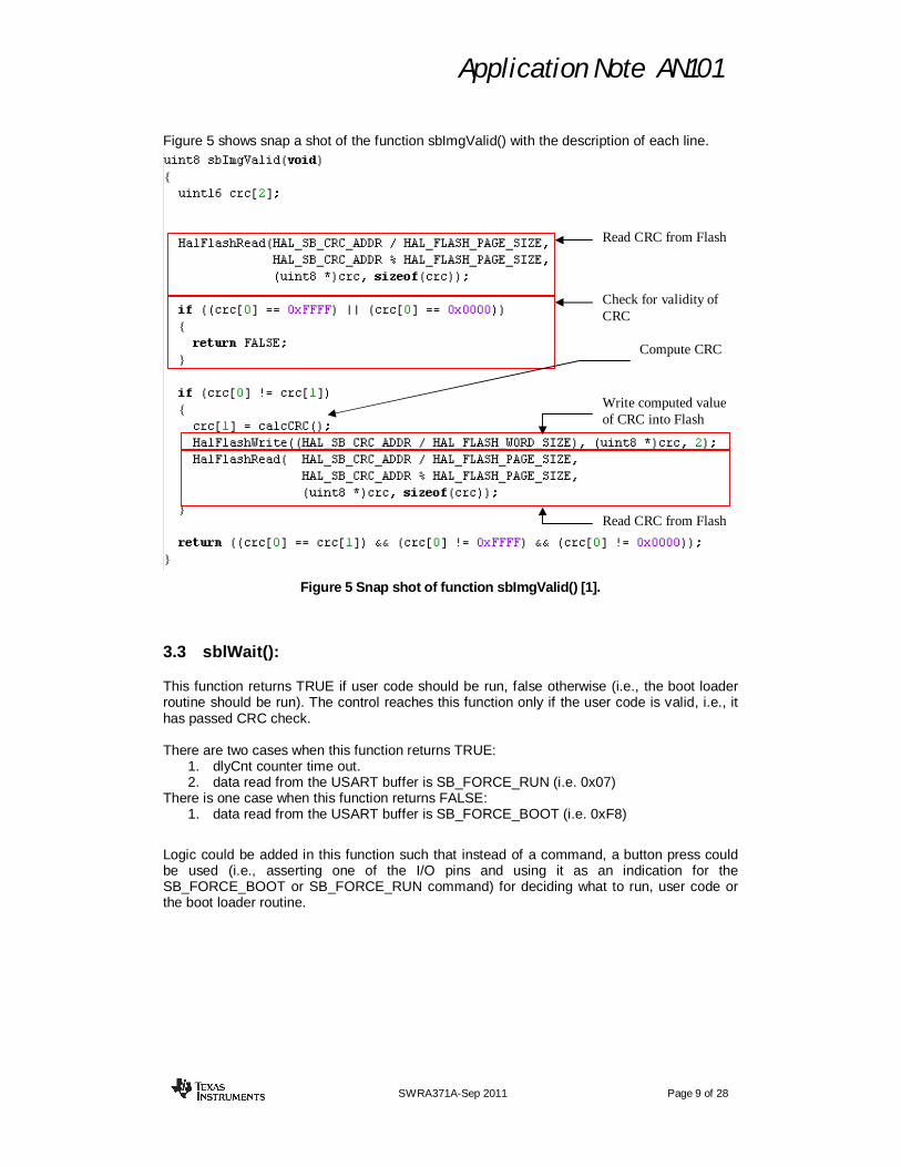
3.2 sbImgValid():
This function checks for validity of the user code. It does so by checking the CRC word that was stored in the flash while writing the user code. The boot loader computes the CRC of the user code and stores it in location 0x2090 and 0x2092 of flash. It keeps two copies of the computed CRC, which are used while validating the user code.
1. First it reads 2 words of CRC from the flash memory (i.e., locations 0x2090 & 0x2092) and stores it in the local array crc[0] and crc[1].
2. Then it checks if crc[0] = 0xFFFF (memory was flushed/erased) or 0x0000 (memory was invalidated). If so, then return FALSE which means user image is not valid.
3. If crc[0] is neither 0xFFFF nor 0x0000, then check if crc[0] = crc[1]. If not, then compute crc on the user code and compare it with the stored crc value in the flash. If they match, then the user code is valid and so return TRUE else return FALSE.
Application Note AN101
SWRA371A-Sep 2011 Page 9 of 28
Figure 5 shows snap a shot of the function sbImgValid() with the description of each line.
Figure 5 Snap shot of function sbImgValid() [1].
3.3 sblWait():
This function returns TRUE if user code should be run, false otherwise (i.e., the boot loader routine should be run). The control reaches this function only if the user code is valid, i.e., it has passed CRC check. There are two cases when this function returns TRUE:
1. dlyCnt counter time out. 2. data read from the USART buffer is SB_FORCE_RUN (i.e. 0x07)
There is one case when this function returns FALSE: 1. data read from the USART buffer is SB_FORCE_BOOT (i.e. 0xF8)
Logic could be added in this function such that instead of a command, a button press could be used (i.e., asserting one of the I/O pins and using it as an indication for the SB_FORCE_BOOT or SB_FORCE_RUN command) for deciding what to run, user code or the boot loader routine.
Read CRC from Flash
Write computed value of CRC into Flash
Read CRC from Flash
Compute CRC
Check for validity of CRC

Application Note AN101
SWRA371A-Sep 2011 Page 10 of 28
Figure 6 Snap shot of the function sblWait() [1].
3.4 HalUARTUnInitISR():
Before jumping to the user code at location 0x2000, we need to reset the USART. So we disable UTX0IE interrupt, UxCSR, URX0IE, URX0IF & UTX0IF. This is done to return the USART to the state it would normally be in after a Hard Reset event.
3.5 sblExec():
1. It checks for the VDD voltage level.
2. It enables interrupts.
3. Finally, it waits in the infinite loop till the sbExec() function returns TRUE. sbExec() returns TRUE when an ENABLE command is given by the external host to the boot loader, which means that complete valid user code is written into the flash memory and the CRC is updated.
3.6 sbExec():
This function contains the state machine that controls the reading/writing of the code into and out of the flash memory.
Read data from USART buffer and return TRUE or FALSE based on command received
If counter “dlyCnt” has reached zero, then return TRUE
Blink LEDs to indicate wait cycle in process
//return FALSE
//return TRUE
//return TRUE
This counter controls the wait time before jumping to user code. Change this value to increase or decrease the wait time.
Application Note AN101
SWRA371A-Sep 2011 Page 11 of 28
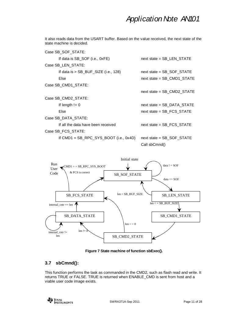
It also reads data from the USART buffer. Based on the value received, the next state of the state machine is decided. Case SB_SOF_STATE:
If data is SB_SOF (i.e., 0xFE) next state = SB_LEN_STATE
Case SB_LEN_STATE:
If data is > SB_BUF_SIZE (i.e., 128) next state = SB_SOF_STATE
Else next state = SB_CMD1_STATE
Case SB_CMD1_STATE:
next state = SB_CMD2_STATE
Case SB_CMD2_STATE:
If length != 0 next state = SB_DATA_STATE
Else next state = SB_FCS_STATE
Case SB_DATA_STATE:
If all the data have been received next state = SB_FCS_STATE
Case SB_FCS_STATE:
If CMD1 = SB_RPC_SYS_BOOT (i.e., 0x4D) next state = SB_SOF_STATE
Call sbCmnd()
Figure 7 State machine of function sbExec().
3.7 sbCmnd():
This function performs the task as commanded in the CMD2, such as flash read and write. It returns TRUE or FALSE. TRUE is returned when ENABLE_CMD is sent from host and a viable user code image exists.
SB_SOF_STATE
SB_LEN_STATE
SB_CMD1_STATE
SB_CMD2_STATE
SB_DATA_STATE
SB_FCS_STATE
Initial state data ! = SOF
data == SOF
len > SB_BUF_SIZE
len < = SB_BUF_SIZE
len != 0
len = = 0
CMD1 = = SB_RPC_SYS_BOOT Run User Code
internal_cntr != len
internal_cntr == len
& FCS is correct

Application Note AN101
SWRA371A-Sep 2011 Page 12 of 28
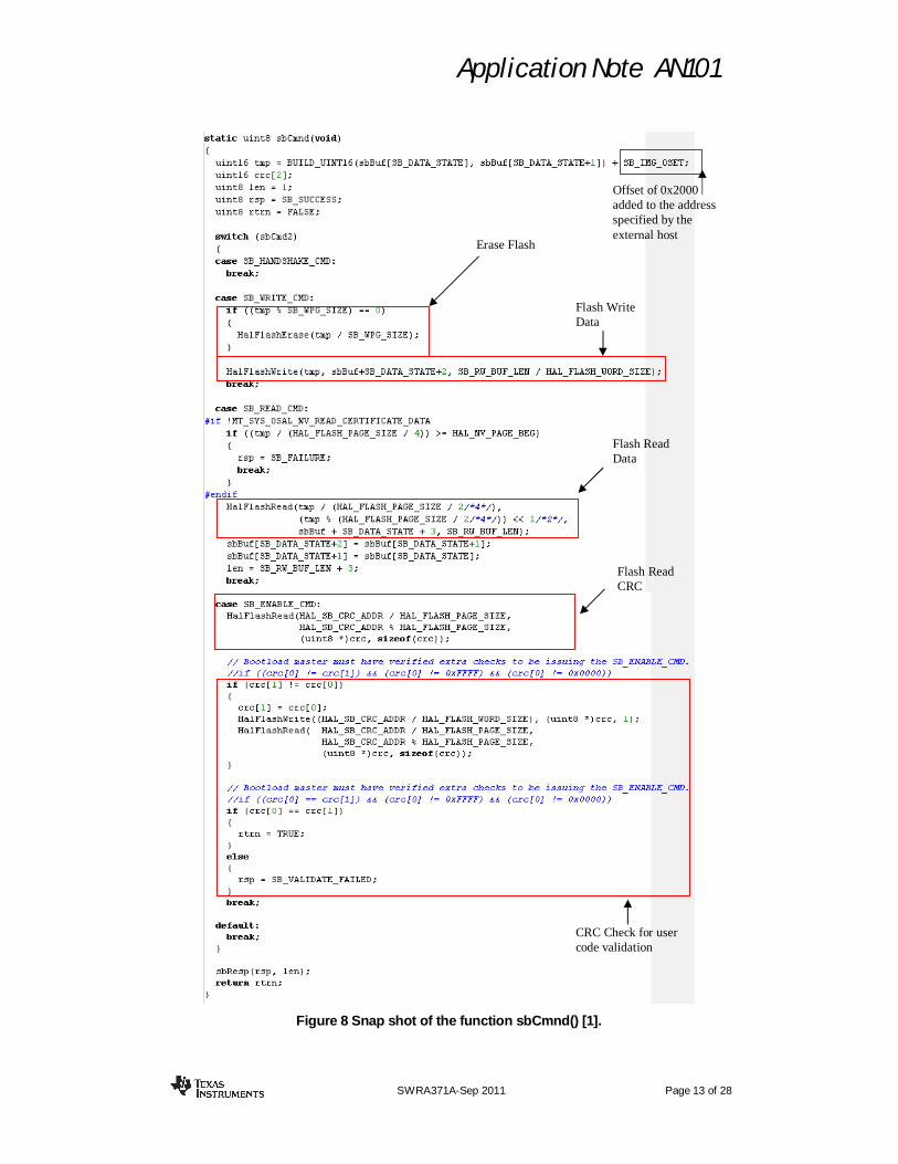
Case SB_HANDSHAKE_CMD:
Return FALSE
Case SB_WRITE_CMD:
Erase flash
Write data into flash
Return FALSE
Case SB_READ_CMD:
Read data from flash
Return FALSE
Case SB_ENABLE_CMD:
Read CRC from flash
Check CRC bytes to find the validity of the user code
If CRC is correct Return TRUE
Else Return FALSE
Command 2 (CMD2) Task Description
0x01 Flash Write Writes 64 bytes of data into internal flash of SoC. Starting address is
specified in the first two bytes of the 66 bytes of the data field of the write frame.
0x02 Flash Read Reads 64 bytes of data from internal flash of SoC. Starting address is specified in the 2 bytes of data field of the read frame.
0x03 Enable Command After complete user code is written into the flash, a frame is sent with the enable command, which will bring control out of the boot loader routine.
0x04 Hand Shake This command should be given before writing user code into flash, just to confirm that execution of boot loader routine has begun.
Table 1 Different types of commands which can be given to the boot loader [1].
Note: Each location in the flash should be erased before writing into it. If the location is not erased before writing, the flash will not be written to the correct value. This is because during a write operation, a flash bit can be changed from a high to a low value, but the bit cannot be changed from low to high [3][7]. This can only be done by an erase command. Erasing a flash will set all the bits of a flash. Now, when a write request comes for writing logic 0, the bit will be changed from 1 to 0 and for writing 1, the bit will be kept unchanged. The smallest unit which can be erased in a flash is called a “Page,” which is 1024 bytes in the case of the CC2510/1 and CC1110/1 SoCs [3][7]. We cannot erase one location at a time; we have to erase one complete page at a time. In this boot loader, we give write requests of 64 bytes at a time. The function sbCmnd() erases the page whenever there is a write request at the starting location of that page. For example whenever there is a request for a write command at location 0x0000 (word address), that means there is a write request at location 0x2000 to 0x2040 (as there is an internal offset of 0x2000 added to the address field, refer to Figure 12 Command frame format.). So page 8 is erased. There will not be a page erase request for other locations within that page, such as 0x2040, 0x2080, etc. Page erase requests come for the following byte addresses: 0x2400, 0x2800, 0x2C00 and so on (LSB 10 bits are zero). In short, the external host cannot start writing from the middle of the page. It will have to start writing from the first location of the page.
Application Note AN101
SWRA371A-Sep 2011 Page 13 of 28
Figure 8 Snap shot of the function sbCmnd() [1].
Erase Flash
Flash Write Data
Flash Read Data
Flash Read CRC
CRC Check for user code validation
Offset of 0x2000 added to the address specified by the external host
Application Note AN101
SWRA371A-Sep 2011 Page 14 of 28
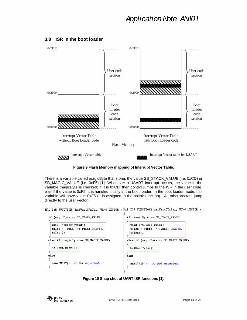
3.8 ISR in the boot loader
Figure 9 Flash Memory mapping of Interrupt Vector Table.
There is a variable called magicByte that stores the value SB_STACK_VALUE (i.e. 0xCD) or SB_MAGIC_VALUE (i.e. 0xF5) [1]. Whenever a USART interrupt occurs, the value in the variable magicByte is checked; if it is 0xCD, then control jumps to the ISR in the user code, else if the value is 0xF5, it is handled locally in the boot loader. In the boot loader mode, this variable will have value 0xF5 (it is assigned in the sblInit function). All other vectors jump directly to the user vector.
Figure 10 Snap shot of UART ISR functions [1].
0x2000 0x2000
0x0000 0x0000
Interrupt Vector Table without Boot Loader code
Interrupt Vector Table with Boot Loader code
Flash Memory
0x7FFF 0x7FFF
Boot Loader
code section
Boot Loader
code section
User code section
User code section
Interrupt Vector table Interrupt Vector table for USART
Application Note AN101
SWRA371A-Sep 2011 Page 15 of 28
The boot loader code should be linked using the sb_boot.xcl linker command file [5]. This file contains the appropriate placement for the boot loader in the first segment of flash. The user code should be linked with an appropriately modified linker command file which places the magicNumber variable at location 0x0001, and the ISR vector table for the user code placed at address 0x2000. Also, the CRC word (16-bits) should be placed at addresses 0x2090-0x2091 and 0x2092-2093 (or word address 0x1048 and 0x1049). Both the locations should have the same CRC word value. NOTE: Upon entering the user code (suggested first thing in main) and before any interrupts are enabled, the user must write the SB _STACK_VALUE to the location referenced by the magicNumber variable. Failure to do so will cause UART interrupts to be ignored or possibly run the boot loader ISR rather than the user ISR. Only after this value is written is it safe for the user code to enable interrupts.
3.9 DMA controller for flash write
The DMA controller is used to write data (user code), which is received from the external host, into the internal flash of the SoC, in chunks of 64 bytes (32 words). (Please refer to the Flash Controller chapter of CC2510/1 or CC1110/1 datasheet for details on DMA flash write [3][7].) In this boot loader, channel 0 of the DMA is used. All DMA parameters such as source address, destination address, transfer count, byte/word transfer, etc., are written into a local structure called “dmaCh0,” and the address of this structure is written into the DMA configuration register DMA0CFGH (0xD5) and DMA0CFGL (0xD4). By setting the values of this structure (dmaCh0), all the parameters of DMA (channel 0) will be set, and, when a trigger event occurs, the DMA will transfer 4 bytes, 1 byte at a time, to the FWDATA register. The DMA trigger is set on Flash data write complete; i.e., whenever a flash data write event occurs, the DMA will start its iteration of writing the data into the FWDATA register incrementing the source address looking at the number of remaining data to transfer (please refer to DMA controller section 12.5 of CC2510/1 or CC1110/1 datasheet). [3][7] All the parameters of DMA are given below:
1. Source address (SRCADDR) (16-bits) – address where the received user code is temporarily stored in SRAM
2. Destination address (DESTADDR) (16-bits) – address of the FWDATA register, i.e., 0x6273
3. Transfer count (16-bits) – 64, i.e., 64-bytes are transferred for each write command.
4. Byte or word transfer (1-bit) – ‘0’, i.e., 1-byte at a time
5. Transfer mode (TMODE) (2-bits) – ‘00’, i.e., single transfer mode
6. Trigger event (TRIG) (5-bits) – ‘10010’, i.e., trigger DMA on flash data write complete
7. Source increment (SRCINC) (2-bits) – ‘01’, i.e., increment source address by 1
8. Destination increment (DESTINC) (2-bits) – ‘00’, i.e., does not increment the destination address as the destination address is FWDATA.
9. Interrupt mask (IRQMASK) (1-bit) – ‘0’, i.e., disable interrupt generation
10. Mode 8 setting (M8) (1-bit) – ‘0’, i.e., use all 8-bits for transfer count
11. DMA priority (PRIORITY) (2-bits) – ‘10’, i.e., DMA access will always prevail over CPU access
After all these parameters are set, the flash address where data needs to be stored is written in its configuration registers FADDH:FADDL, and then FCTL.WRITE is set. This will trigger the DMA write and will wait till FCTL.BUSY becomes zero, i.e., the flash write is complete.

Application Note AN101
SWRA371A-Sep 2011 Page 16 of 28
4 Frame Format
In this section, we will discuss the frame format in which an external host can interact and command the boot loader to perform various tasks like writing into the internal flash, reading from the internal flash and exiting the boot loader routine. Before looking into the details of the frame format, let us look at an example flow of a write command and its response (Figure 11).
Figure 11 Example of flow of data write command and its response.
First, the external host will generate a frame, as shown in Figure 11, and will start driving this frame into the boot loader through the SPI bus. This write command frame will have a total length of 71 bytes with 66 bytes of payload (2 bytes of address field followed by 64 bytes of data field) [1] shown in light blue in Figure 11. Once the boot loader receives this frame, it will call function sbCmnd(), where this frame is detected as a write frame (by looking at CMD2). The boot loader will then write the data into the internal flash of SoC, starting at the location specified in the address field of the frame. The boot loader uses DMA to write the data into flash (discussed in section 3.9). Once all the data has been written into the flash, the sbResp() function is called in which a response frame is generated by the boot loader and written into the USART buffer. The external host can then read the response by issuing a read request on the SPI bus. Keep a wait cycle (say 50 msec) before reading the response, because the boot loader may take some time to generate and write the response into the USART buffer. The response frame will be 6 bytes long with one byte of data, i.e., the response field. Response = 0x00 means that the command has been performed successfully. There can be N such write commands to write the complete user code into the internal flash. Address field will start with 0x0000, as there is an internal offset of 0x2000 added to this address field. On every write command 64 bytes of data is written into the flash. So the address needs to be incremented by 0x0020 (i.e. 32) each time a write command is given because the addressing mode is word address (each word is 16-bits long) and not byte address. For example, if there are 5 write commands, then the address field of first write command will be 0x0000, the address field of second write command will be 0x0020, the address field of third write command will be 0x0040, then 0x0060 and so on.
SOF CMD1 CMD2 LEN
A A D D D D D
Addr Addr
DATA DATA
DATA DATA
DATA FCS
0xFE 0x4D 0x01 0x42
0x00 0x00
0xXX 0xXX
0xXX 0xXX
0xXX
SOF CMD1 CMD2 LEN
RESP
0xFE 0x4D 0x81 0x01
0x00
FCS
0xFE 0x42
SOF LEN
Write data into Flash
Call sbCmnd()
Call sbResp()
Return to sbExec()
Length = 0x42
CMD2 = CMD2 | 0x80
Application Note AN101
SWRA371A-Sep 2011 Page 17 of 28
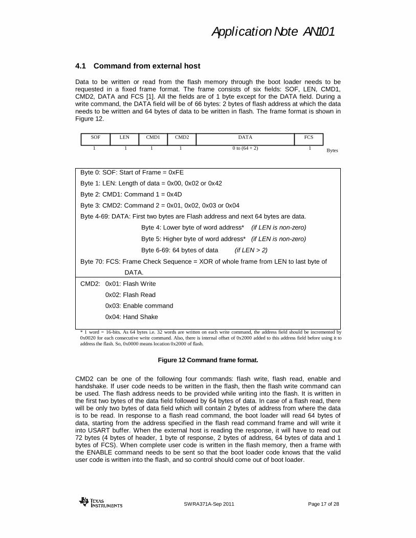
4.1 Command from external host
Data to be written or read from the flash memory through the boot loader needs to be requested in a fixed frame format. The frame consists of six fields: SOF, LEN, CMD1, CMD2, DATA and FCS [1]. All the fields are of 1 byte except for the DATA field. During a write command, the DATA field will be of 66 bytes: 2 bytes of flash address at which the data needs to be written and 64 bytes of data to be written in flash. The frame format is shown in Figure 12.
Figure 12 Command frame format.
CMD2 can be one of the following four commands: flash write, flash read, enable and handshake. If user code needs to be written in the flash, then the flash write command can be used. The flash address needs to be provided while writing into the flash. It is written in the first two bytes of the data field followed by 64 bytes of data. In case of a flash read, there will be only two bytes of data field which will contain 2 bytes of address from where the data is to be read. In response to a flash read command, the boot loader will read 64 bytes of data, starting from the address specified in the flash read command frame and will write it into USART buffer. When the external host is reading the response, it will have to read out 72 bytes (4 bytes of header, 1 byte of response, 2 bytes of address, 64 bytes of data and 1 bytes of FCS). When complete user code is written in the flash memory, then a frame with the ENABLE command needs to be sent so that the boot loader code knows that the valid user code is written into the flash, and so control should come out of boot loader.
SOF LEN CMD1 CMD2 DATA FCS
1 1 1 1 1 0 to (64 + 2) Bytes
Byte 0: SOF: Start of Frame = 0xFE
Byte 1: LEN: Length of data = 0x00, 0x02 or 0x42
Byte 2: CMD1: Command 1 = 0x4D
Byte 3: CMD2: Command 2 = 0x01, 0x02, 0x03 or 0x04
Byte 4-69: DATA: First two bytes are Flash address and next 64 bytes are data.
Byte 4: Lower byte of word address* (if LEN is non-zero)
Byte 5: Higher byte of word address* (if LEN is non-zero)
Byte 6-69: 64 bytes of data (if LEN > 2)
Byte 70: FCS: Frame Check Sequence = XOR of whole frame from LEN to last byte of
DATA.
CMD2: 0x01: Flash Write
0x02: Flash Read
0x03: Enable command
0x04: Hand Shake
* 1 word = 16-bits. As 64 bytes i.e. 32 words are written on each write command, the address field should be incremented by 0x0020 for each consecutive write command. Also, there is internal offset of 0x2000 added to this address field before using it to address the flash. So, 0x0000 means location 0x2000 of flash.

Application Note AN101
SWRA371A-Sep 2011 Page 18 of 28
Figure 13 Typical sequence of command to write user code.
Figure 13 shows a typical sequence of frames to write user code into the flash memory. It starts with handshake frame, which just acknowledges the external host (who is issuing the command) that the boot loader routine is running. Then the external host can start sending frames with a write command to write the user code into specified flash addresses (starting with 0x0000 and then incrementing by 0x0020 for each write command). Once the whole user code is written into the flash, a frame with an enable command is issued that will inform the boot loader that valid user code has been written into the flash and so boot loader execution should end and control should jump to the user code. Before giving the enable command, a read command can be used to read the flash and verify that the user code is written correctly into the flash (optional). Note: The data (which is the user code) passed through the frame is in binary format. Data is directly written into the flash without any processing or modification on it. Insert CRC word (16-bits) at two locations: Word address - 0x0048 and 0x0049 (0x1000 will be added by boot loader) In terms of byte address it will be 0x0090-0x0091 and 0x0092-0x0093. (0x2000 will be added by boot loader)
Frame 2 Frame 3 Frame N-1 Frame N
Write command Enable command
Frame 1
Write command Write command Handshake command
Application Note AN101
SWRA371A-Sep 2011 Page 19 of 28
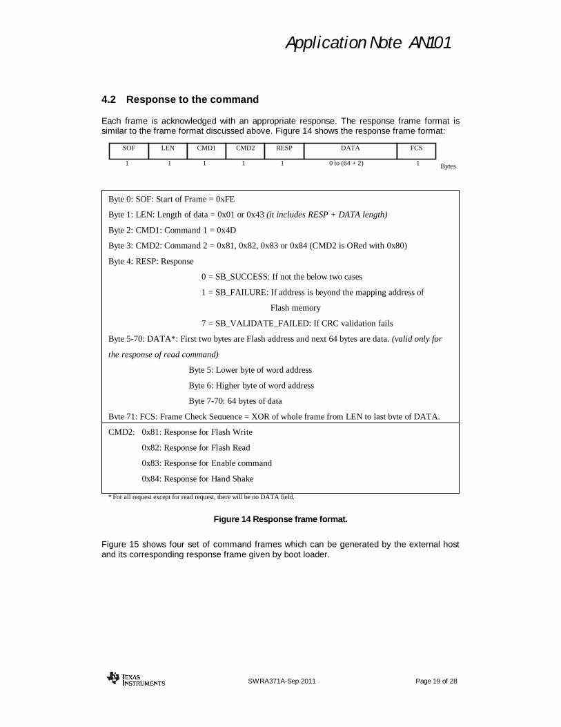
4.2 Response to the command
Each frame is acknowledged with an appropriate response. The response frame format is similar to the frame format discussed above. Figure 14 shows the response frame format:
Figure 14 Response frame format.
Figure 15 shows four set of command frames which can be generated by the external host and its corresponding response frame given by boot loader.
SOF LEN CMD1 CMD2 DATA FCS
1 1 1 1 1 0 to (64 + 2) Bytes
Byte 0: SOF: Start of Frame = 0xFE
Byte 1: LEN: Length of data = 0x01 or 0x43 (it includes RESP + DATA length)
Byte 2: CMD1: Command 1 = 0x4D
Byte 3: CMD2: Command 2 = 0x81, 0x82, 0x83 or 0x84 (CMD2 is ORed with 0x80)
Byte 4: RESP: Response
0 = SB_SUCCESS: If not the below two cases
1 = SB_FAILURE: If address is beyond the mapping address of
Flash memory
7 = SB_VALIDATE_FAILED: If CRC validation fails
Byte 5-70: DATA*: First two bytes are Flash address and next 64 bytes are data. (valid only for
the response of read command)
Byte 5: Lower byte of word address
Byte 6: Higher byte of word address
Byte 7-70: 64 bytes of data
Byte 71: FCS: Frame Check Sequence = XOR of whole frame from LEN to last byte of DATA.
CMD2: 0x81: Response for Flash Write
0x82: Response for Flash Read
0x83: Response for Enable command
0x84: Response for Hand Shake
RESP
1
* For all request except for read request, there will be no DATA field.

Application Note AN101
SWRA371A-Sep 2011 Page 20 of 28
Figure 15 Command frame and its corresponding response frame.
Figure 16 shows waveforms for the data transfer on the SPI bus. As seen in the waveforms, read and write cycles are exactly same. The only difference is that, in a write cycle, SIMO is driven with valid data and the SoC will drive SOMI with the value present in its TXBUF. In case of a read cycle, SIMO can be driven with any value (say 0x00) other than the key bytes (like 0xFE, 0x4D, etc) which represents the command to the SoC, and the SOMI value is sampled on each rising edge of SCLK. In short, the SoC will always read the value of SIMO and store it in its internal RXBUF and will always drive value stored in TXBUF on the SOMI pin.
Command Response
Handshake
Write
Read
Enable
FE 00 4D 04 49 FE 01 4D 84 00 C8
FE 01 4D 81 00 CD
FE 43 4D 82 00 XX XX XX
FE 42 4D 01 XX XX XX
FE 01 4D 83 00 CF FE 00 4D 03 4E
FE 02 4D 02 XX XX XX
64 bytes
64 bytes
SOF LEN CMD1 CMD2 Addr FCS
RESP DATA

Application Note AN101
SWRA371A-Sep 2011 Page 21 of 28
Figure 16 Waveform for data transfer on SPI bus [4].
SIMO
SOMI
SCLK
CS_N
Don’t care Note: Please refer to the CC2510/1 or CC1110/1 data sheet for the timing parameters
Write Read

Application Note AN101
SWRA371A-Sep 2011 Page 22 of 28
5 Test Environment
In this section, we describe the setup used for burning the boot loader code into the location 0x0000 to 0x1FFF (byte address) of the internal flash using IAR embedded workbench for 8051 and the interface with the external host, which will be writing valid user code into locations 0x2000 to 0x7FFF (byte addresses) of the internal flash of the SoC.
Figure 17 Test Environment setup to burn the boot loader code into SoCs and to interact
with external host for writing valid user code into the internal flash of SoCs.
[3][4][7] The SPI interface is used to communicate between an external host and the boot loader. This can be easily changed to a UART interface by just configuring USART registers in the HalUARTInitISR() function. Port P1.0 is set as an output port, which can be used as indication at various stages of the code (for debugging purposes). To program the SoC with the boot loader code using IAR Embedded workbench, the P2.1 and P2.2 pins are used as debug data and debug clock pins respectively. The code is built and programmed through IAR workbench by opening the workspace: $PROJ_DIR\ boot_loader\boot.eww. In this setup, Port 0 is configured in SPI mode. Port 1 can also be used instead of Port 0. This can be done in sblInit() function. Make sure to define CC2510, CC2511, CC1110 or CC1111 in the options C/C++ Compiler Preprocessor Defined symbols in IAR embedded work bench, based on which SoC the boot loader is being burned. This will include the appropriate I/O header file from the following folder: <IAR installed folder>\8051\inc\ioCC2510.h (or ioCC2511.h / ioCC1110.h / ioCC1111.h). IAR workbench version 7.6 was used for building this project, so it’s recommended to use this or any newer version.
CC2510/1 or CC1110/1 SoC
External Host SPI bus
P0.4
P0.5
P0.3
P0.2 CS_N
SCLK
SIMO
SOMI
GND
P1.0
DC DD
Programming through IAR Embedded
workbench Used as indication for debugging
purpose. Can also be directly
connected to oscilloscope
instead of LED
P2.1
P2.2
Debug interface
RESET_N
RESET_N
Application Note AN101
SWRA371A-Sep 2011 Page 23 of 28
6 Sample LED blinking code
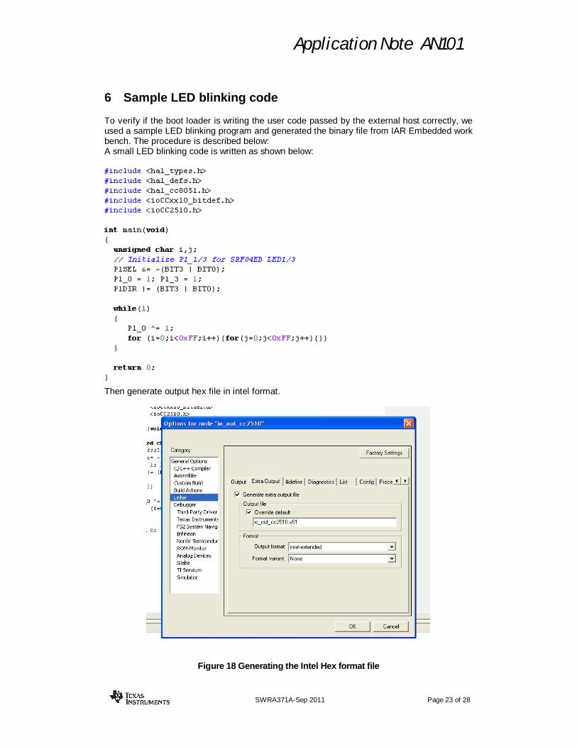
To verify if the boot loader is writing the user code passed by the external host correctly, we used a sample LED blinking program and generated the binary file from IAR Embedded work bench. The procedure is described below: A small LED blinking code is written as shown below:
Then generate output hex file in intel format.
Figure 18 Generating the Intel Hex format file

Application Note AN101
SWRA371A-Sep 2011 Page 24 of 28
Before compiling and generating the Intel Hex file, we will have to change the starting address of the code in the linker file to 0x2000. This is done because we are not writing the code at location 0x0000; we are relocating it to location 0x2000, and if the compiler used absolute jump instead of relative jump commands, control would move to the wrong location and the code might hang. Figure 19 shows the snap shot of the IAR workbench showing the path of the linker file where the starting address needs to be changed [8].
Figure 19 Changing the program starting address
It will generate a file in standard Intel HEX file format [9] as shown below: :020000040000FA
:1000000002001700000080FB120020B9000302006C
:100010001112002312000375D0007581BF02000881
:1000200079012253F4F6E5F4D290D29343FE09E528
:10003000FE639001E5907B0080080AEAC394FF40CC
:0C004000F90BEBC394FF50E97A0080EF4D
:0400000500000017E0
:00000001FF
[Blue: DATA, RED: location to which instruction pointer must point at the beginning] Binary data could be extracted from this file and driven as user code from external host. In the drop-down list of format, there is another format called “msp430-txt” which will generate text file with binary value of the code as shown below: 02 00 17 00 00 00 80 FB 12 00 20 B9 00 03 02 00
11 12 00 23 12 00 03 75 D0 00 75 81 BF 02 00 08
79 01 22 53 F4 F6 E5 F4 D2 90 D2 93 43 FE 09 E5

Application Note AN101
SWRA371A-Sep 2011 Page 25 of 28
FE 63 90 01 E5 90 7B 00 80 08 0A EA C3 94 FF 40
F9 0B EB C3 94 FF 50 E9 7A 00 80 EF
This format will directly give the binary data that needs to be written into the internal flash of the SoC. After writing this code into the flash and giving reset, control will jump to this user code, and the P1.0 pin will start toggling at a rate dependent on system clock. The frames with the command bytes and above data will look like: Frame 1: FE 42 4D 01 00 00 02 00 17 00 00 00 80 FB 12 …… EA C3 94 FF 40 FCS Frame 2: FE 42 4D 01 00 20 F9 0B EB C3 94 FF 50 E9 7A 00 80 EF FF FF FF FF …… FF FF FCS Frame 3: FE 42 4D 01 00 40 FF FF FF FF …… FF FF CD 56 CD 56 FF FF ……. FF FF FF FF FCS The first frame will write first 64 bytes of data in the internal flash starting at location (byte address) 0x2000 + 0x0000 = 0x2000 and ending at location 0x203F. The second frame will write the remaining 12 bytes of data and FF into next 64 locations of internal flash (0x2040 to 0x207F). The third frame is used to write the CRC word into the internal flash. In the third frame, word address 0x0048 = 0x0049 = 0xCD56 (for example), which is the CRC word location (corresponding byte address = 0x0090-0x0091& 0x0092-0x0093) As seen in Intel HEX file, this code starts at location 0x0017 and not 0x0000, so after the boot loader execution is over, control should jump to location 0x2017 and not 0x2000. This location of jump to the user code will depend on the location of the starting point of the user code. Note: Do not forget to write the CRC word in two locations of flash 0x0048 and 0x0049 (word address).
0x0048 0x0049

Application Note AN101
SWRA371A-Sep 2011 Page 26 of 28
7 FAQ
Q1. Is there any option of specifying the start address of the application code (i.e., the address with which the program counter must be loaded initially to run the application code)?
Ans. Yes. There is a LJMP command in the main() function (sb_main.c) which specifies the starting point of the user code. For example, suppose the user code is written from 0x2000 to 0x3000 but the starting point of the application code is 0x2017. Then, the instruction pointer must be loaded with 0x2017, which is done by the command asm(“LJMP 0x2017\n”) in the main() function. You can change this address to the starting address of your application code. Q2. What all changes are required if I need to change the bootloader reserved code space?
Ans. You will require two changes: 1. Change –D_CODE_END variable in sb-boot.xcl 2. Change the offset added to the address sent through the read/write command. This
is done by changing these two values in hal_board_cfg.h a. #define HAL_SB_IMG_ADDR 0x2000 b. #define HAL_SB_CRC_ADDR 0x2090
HAL_SB_IMG_ADDR will change the offset added and HAL_SB_CRC_ADDR indicates the location where computed CRC value is stored. This will also change if boot loader code space increases or decreases.
Q3. While generating application code starting at (for example) location 0x2800, there are some values generated at locations between 0x0000 to 0x008F. What are these and do we need to write these values into flash?
Ans. These are interrupt vectors at locations: 0x0003, 0x000B, 0x0013, 0x001B, 0x0023, 0x002B … till 0x008B. These are total 18 interrupt vectors.
Let’s consider an example. Suppose after generating the hex file, you get @0000 02 28 4D @0013 02 2F 3C @003B 02 2F AE @004B 02 31 69 @0083 02 39 14 @2800 XXXXXXXXXXXXXXXXXXXXXXXXXXXXXXXXXXX XXXXXXXXXXXXXXXXXXXXXXXXXXXXXXXXXXX XXXXXXXXXXXXXXXXXXXXXXXXXXXXXXXXXXX…..
Please follow the below steps to handle these interrupts: 1. Open file interrupt_stubs.s51. There is an offset defined as 0x2000 at line 40. As the
boot loader code area is increased to 0x2800, make this offset as 0x2800 (or whatever is the boot loader code area). What this will do is, for example, write “jump
On reset, control jumps to location 0x0000. So this location contains the starting point of the application code. It is a JUMP to 0x284D command
Interrupt vectors (containing JUMP command to respective ISR)
Application code
Application Note AN101
SWRA371A-Sep 2011 Page 27 of 28
to 0x284B” at location 0x004B when you burn the boot loader code into the SoC (it will do this for all the interrupt vectors). So whenever a timer 1 interrupt comes, the 8051 will move to location 0x004B where the jump to 0x284B command will be written. This way all the interrupt vectors are forwarded to the interrupt vector starting at location 0x2800.
2. In the file interrupt_stubs.s51, you will see that “USART0 RX complete” and “USART0 TX complete” interrupt vectors are commented out. This is because these two interrupts are also used by the boot loader, so we cannot directly forward these interrupts to location 0x2813/0x283B. Whenever one of these two interrupts occurs, the 8051 will move to location 0x0013 or 0x003B (based on the RX/TX interrupt), and there will be jump command that will jump to the if condition within the boot loader code area defined in file sb_main.c (line 379). In this if condition, it checks if boot loader code is running or the application code is running. If the boot loader code is running, this interrupt is handled internally by the boot loader (by calling function halUartRxIsr() or halUartTxIsr()), otherwise it jumps to location 0x2013 or 0x203B. Just change the location value at line 384 from 0x2013 to 0x2813 and at line 402: from 0x203B to 0x283B. This will ensure that when interrupt was from the application code, control jumps to the location 0x2813 or 0x283B
3. There are 18 interrupt vectors (0x2803, 0x280B, 0x2813, 0x281B, 0x2823, 0x282B,…) starting from 0x2803 to 0x288B. So you will have to skip these values while writing application code. Better to start the application code at 0x2900. So change the -D_CODE0_START value to 0x2900 instead of 0x2800 and again generate the msp430-txt format file.
4. Now you will get new values for @0013, @003B, @004B and @0083. Write those values at location 0x00XX (i.e. 0x0003, 0x000B, 0x0013, 0x001B…) or 0x28XX (i.e., 0x2803, 0x280B, 0x2813, 0x281B…). Remember that the current boot loader supports only 64 bytes of write command. So if you would like to write these interrupt vectors at location 0x28XX, write it as shown below:
@0x2800 FF FF FF 02 XX XX FF FF FF FF FF 02 XX XX FF FF FF FF FF 02 XX XX FF FF FF FF FF 02 XX XX FF FF FF FF FF 02 XX XX FF FF FF FF FF 02 XX XX FF FF FF FF FF 02 XX XX FF FF FF FF FF 02 XX XX FF FF @0X2840 FF FF FF 02 XX XX FF FF FF FF FF 02 XX XX FF FF FF FF FF 02 XX XX FF FF FF FF FF 02 XX XX FF FF FF FF FF 02 XX XX FF FF FF FF FF 02 XX XX FF FF FF FF FF 02 XX XX FF FF FF FF FF 02 XX XX FF FF @0X2880 FF FF FF 02 XX XX FF FF FF FF FF 02 XX XX FF FF FF FF FF FF FF FF FF FF FF FF FF FF FF FF FF FF FF FF FF FF FF FF FF FF FF FF FF FF FF FF FF FF FF FF FF FF FF FF FF FF FF FF FF FF FF FF FF FF (numbers in red are the jump command of the four interrupts generated after compilation) (You can start writing at location 0x2800 and fill 0xFF in all the intermediate locations (i.e. non-interrupt vector locations)) You can write FF for the interrupts which you are not using. So there will be 3 write requests of 64 bytes each. As address given during write command is word address, you will have to give 0x1400, 0x1420 and 0x1440 for the three write commands. In this case you will have to write 0x2813 and 0x283B in the HAL_ISR_FUNCTION() in file sb_main.c

Application Note AN101
SWRA371A-Sep 2011 Page 28 of 28
8 References
8.1 Cited references
[1] CC253x Bootloader code in ZigBee protocol stack for CC2530 - http://focus.ti.com/docs/toolsw/folders/print/z-stack.html
[2] CC253x SoC User’s Guide - http://focus.ti.com/docs/prod/folders/print/cc2530.html
[3] CC2510/1 datasheet - http://focus.ti.com/docs/prod/folders/print/cc2510f32.html
[4] TI design note DN113 on CC111xFx, CC243xFx,CC251xFx and CC253xFx SPI interface - http://www.ti.com/lit/swra223
[5] Serial Boot Loader for CC253x SoC, Document number: SWRA327 http://focus.ti.com/docs/toolsw/folders/print/z-stack.html
[6] CC2510/1 & CC1110/1 Bootloader code - http://www.ti.com/litv/zip/swra371 [7] CC1110/1 datasheet -
http://focus.ti.com/docs/prod/folders/print/cc1110f32.html
8.2 General references
[8] IAR Embedded workbench - http://www.iar.com/website1/1.0.1.0/3/1/ [9] http://en.wikipedia.org/wiki/Intel_HEX
9 Document History
Revision Date Description/Changes 1.0 06/08/2011 Initial release. 1.1 09/07/2011 Support for CC2511, CC1110 and CC1111.
IMPORTANT NOTICE
Texas Instruments Incorporated and its subsidiaries (TI) reserve the right to make corrections, modifications, enhancements, improvements,and other changes to its products and services at any time and to discontinue any product or service without notice. Customers shouldobtain the latest relevant information before placing orders and should verify that such information is current and complete. All products aresold subject to TI’s terms and conditions of sale supplied at the time of order acknowledgment.
TI warrants performance of its hardware products to the specifications applicable at the time of sale in accordance with TI’s standardwarranty. Testing and other quality control techniques are used to the extent TI deems necessary to support this warranty. Except wheremandated by government requirements, testing of all parameters of each product is not necessarily performed.
TI assumes no liability for applications assistance or customer product design. Customers are responsible for their products andapplications using TI components. To minimize the risks associated with customer products and applications, customers should provideadequate design and operating safeguards.
TI does not warrant or represent that any license, either express or implied, is granted under any TI patent right, copyright, mask work right,or other TI intellectual property right relating to any combination, machine, or process in which TI products or services are used. Informationpublished by TI regarding third-party products or services does not constitute a license from TI to use such products or services or awarranty or endorsement thereof. Use of such information may require a license from a third party under the patents or other intellectualproperty of the third party, or a license from TI under the patents or other intellectual property of TI.
Reproduction of TI information in TI data books or data sheets is permissible only if reproduction is without alteration and is accompaniedby all associated warranties, conditions, limitations, and notices. Reproduction of this information with alteration is an unfair and deceptivebusiness practice. TI is not responsible or liable for such altered documentation. Information of third parties may be subject to additionalrestrictions.
Resale of TI products or services with statements different from or beyond the parameters stated by TI for that product or service voids allexpress and any implied warranties for the associated TI product or service and is an unfair and deceptive business practice. TI is notresponsible or liable for any such statements.
TI products are not authorized for use in safety-critical applications (such as life support) where a failure of the TI product would reasonablybe expected to cause severe personal injury or death, unless officers of the parties have executed an agreement specifically governingsuch use. Buyers represent that they have all necessary expertise in the safety and regulatory ramifications of their applications, andacknowledge and agree that they are solely responsible for all legal, regulatory and safety-related requirements concerning their productsand any use of TI products in such safety-critical applications, notwithstanding any applications-related information or support that may beprovided by TI. Further, Buyers must fully indemnify TI and its representatives against any damages arising out of the use of TI products insuch safety-critical applications.
TI products are neither designed nor intended for use in military/aerospace applications or environments unless the TI products arespecifically designated by TI as military-grade or "enhanced plastic." Only products designated by TI as military-grade meet militaryspecifications. Buyers acknowledge and agree that any such use of TI products which TI has not designated as military-grade is solely atthe Buyer's risk, and that they are solely responsible for compliance with all legal and regulatory requirements in connection with such use.
TI products are neither designed nor intended for use in automotive applications or environments unless the specific TI products aredesignated by TI as compliant with ISO/TS 16949 requirements. Buyers acknowledge and agree that, if they use any non-designatedproducts in automotive applications, TI will not be responsible for any failure to meet such requirements.
Following are URLs where you can obtain information on other Texas Instruments products and application solutions:
Products Applications
Audio www.ti.com/audio Communications and Telecom www.ti.com/communications
Amplifiers amplifier.ti.com Computers and Peripherals www.ti.com/computers
Data Converters dataconverter.ti.com Consumer Electronics www.ti.com/consumer-apps
DLP® Products www.dlp.com Energy and Lighting www.ti.com/energy
DSP dsp.ti.com Industrial www.ti.com/industrial
Clocks and Timers www.ti.com/clocks Medical www.ti.com/medical
Interface interface.ti.com Security www.ti.com/security
Logic logic.ti.com Space, Avionics and Defense www.ti.com/space-avionics-defense
Power Mgmt power.ti.com Transportation and Automotive www.ti.com/automotive
Microcontrollers microcontroller.ti.com Video and Imaging www.ti.com/video
RFID www.ti-rfid.com
OMAP Mobile Processors www.ti.com/omap
Wireless Connctivity www.ti.com/wirelessconnectivity
TI E2E Community Home Page e2e.ti.com
Mailing Address: Texas Instruments, Post Office Box 655303, Dallas, Texas 75265Copyright © 2011, Texas Instruments Incorporated